Embed Size (px)
Citation preview
Damage Recovery by Reductive Chemistry after Methanol-Based Plasma Etch
to Fabricate Magnetic Tunnel Junctions
Keizo Kinoshita1, Tadashi Yamamoto2, Hiroaki Honjo1, Naoki Kasai1, Shoji Ikeda1;3, and Hideo Ohno1;3
1Center for Spintronics Integrated Systems, Tohoku University, Sendai 980-8577, Japan2ULVAC, Inc., Susono, Shizuoka 410-1231, Japan3Research Institute of Electrical Communication, Tohoku University, Sendai 980-8577, Japan
Received November 28, 2011; accepted February 29, 2012; published online August 20, 2012
The damage recovery process for magnetic tunnel junctions (MTJs) after methanol- (Me-OH) based plasma etch has been demonstrated. Me-OH
and O2 plasma, which contain oxygen in the molecule, caused unavoidable modification of magnetic materials in the MTJ stack. For example, the
magnetization saturation and MR ratio decreased. H2 base reductive plasma treatment was effective in recovering from this deterioration. No
harmful side effects were observed in other aspects of MTJ performance such as MTJ resistance, hysteresis loop offset, and switching field.
Heavier initial damage required a longer treatment time for recovery. Other types of reductive chemistry such as NH3 plasma deteriorated the MTJ
when the treatment lasted more than 15 s, probably due to nitridation. The use of a highly selective Ar/Me-OH etch process along with He/H2
plasma recovery treatment is very promising for the MTJs’ etch process to fabricate high-density magnetic random access memory (MRAM) and
non-volatile logic devices. # 2012 The Japan Society of Applied Physics
1. Introduction
Demand for a magnetic tunnel junction (MTJ) fine etchtechnique has increased in order to achieve large capacitymagnetic random access memory (MRAM)1) as well as non-volatile logic devices.2)
One of the reasons for this demand is the ‘‘GreenInnovation’’ concept, which is becoming increasinglycommon. Efforts will continue to be made to realizesustainable development for the next generations.3) Im-proving the efficiency of electricity usage is an importanttarget to reduce total CO2 emissions. Zero-standby-powersystems would be an effective means of addressing thisissue.4) To achieve such systems, it is necessary to developa non-volatile logic core as well as a non-volatile cachememory with adequate operating software. The memoryelements used in these core LSI parts must have anunlimited overwriting feature. Many non-volatile memoryelements have been proposed. However, up to now, theMTJ was the only element that had the unlimitedoverwriting feature.5) Therefore, attempts have been madeto apply MTJs in flip-flop circuits as the start line of thezero-standby-power devices,6) as well as some functionallogic devices.7)
Another reason for the increased demand is the improve-ment in MTJ performance compared to the first-generationMRAM.8) MRAM reported recently is approaching theoperating speed9) and capacity10) that will enable it toreplace existing embedded memory applications. In addi-tion, some breakthrough technologies have been proposed toovercome the other issues. For example, low-write-currentcell technology has been proposed that uses magneticdomain wall motion by spin-polarized current to change amemory state.11–13) Material developments are also progres-sing day by day. A perpendicular magnetization materialwas proposed that incorporates interfacial anisotropy andthat uses a popular CoFeB/MgO material combination.14,15)
The material can withstand back-end-of-line (BEOL)process temperatures.16) This is very important, especiallyfor embedded memory applications, as the other parts of thedevice must be processed using the standard BEOL processtechnology. Moreover, process technologies that are spe-cially used for MTJ fabrication, for example, ultra-uniform
magnetron sputtering, have also shown important scientificprogress recently.17–19)
Historically, etching technologies for magnetic materialshave mainly been carried out using the following three gaschemistries:1. Argon based chemistry (Ar ion milling, Ar plasma
etch).2. Chlorine based chemistry with elevated temperature
wafer stage (Cl2, BCl3/Cl2).3. C–O(X) based chemistry (NH3/CO, Me-OH, CH4/H2/
O2).First, Ar ion milling has long been used for magnetic
device manufacturing.20,21) It has also been applied in MTJetching on 200mm wafers.22–24) The advantage of the pureAr process is that the process causes little or no chemicaldamage to the magnetic properties. Therefore, efforts havecontinued to apply this milling technique to 300mm wafers.However, it is still difficult to enlarge the ion beam radiuswhile maintaining beam divergence and directionality aswell as beam current uniformity. In addition, one of theimportant advantages of the ion milling system cannot beapplied to high density MTJ patterns, i.e., the ability to applybeam tilt and wafer rotation to etch off redeposited materialfrom the pattern sidewalls. The distance between oneMTJ and the next should be far enough to eliminate theshadowing effect of the ion beam by the wafer tilt androtation. If the height of the MTJ stack including a hardmask is assumed to be �150 nm, and the diameter of theMTJ is assumed to be �50 nm, the allowable beam tilt angleis determined to be more than 71.5� by simply estimating the2F density MTJ.1) This tilt angle value is not sufficient toreduce side wall deposition.
We can apply an Ar sputter etch process with the usualplasma etch apparatus.25) One of the authors reported thatthe process showed almost the same performance with Armilling. The major difficulty in the Ar sputter etch processwas an electrical short failure due to conductive redepositionat the side wall of the MgO barrier.26) A tapered hardmask would make it possible to reduce the short yield byeliminating local etching and redeposition at the bottom ofthe pattern side. However, there is a tradeoff with MTJpattern density. In addition, low etch selectivity of the Arsputter etch requires extremely high etch uniformity and a
Japanese Journal of Applied Physics 51 (2012) 08HA01
08HA01-1 # 2012 The Japan Society of Applied Physics
REGULAR PAPERhttp://dx.doi.org/10.1143/JJAP.51.08HA01
precise etch end-point detection (EPD) technique for multi-stack MTJ structures with nanometer-order thickness foreach layer.
Chlorine-based chemistries have been used with anelevated temperature wafer stage for many years.27,28) Themicrostructure of the standard physical vapor deposition(PVD) magnetic film is columnar, as in PVD aluminum film.Therefore, chlorine-based processing will result in a processissue similar to that of the aluminum etch process, suchas after corrosion, if there is no after treatment proceduresuitable for MTJ stack.
Several approaches have been used that involve C–O(X)-based chemistries; this refers to etch processes using carbon-and oxygen-containing plasma. This was first tried byNakatani in 1996 with an NH3/CO gas mixture.29) Hestated that he ‘‘aimed at the formation of volatile transitionmetal carbonyls’’.29) However, although, the pattern shape isrectangular, and the achieved etch rate of permalloy (NiFe)is high (35 nm/min) compared to conventional ion milling,we must consider about difficulties of the formation of largemolecules of carbonyl compounds in the processing plasma.To date, there has been no reported evidence of metalcarbonyl formation in the processing plasma.
A more recent method using methanol (Me-OH) plasmawas proposed by Osada et al., in 2004.30) This is alsoattributed to C–O-based chemistry. Thanks to the high etchselectivity against Ta hard masks,31) the etch profile of theC–O-based process was more vertical compared to that ofsimple physical etching.32) The major problem with C–O-based chemistry is that magnetic properties tend todegrade.26) The estimated depth of damage from the patternside wall is approximately 5 to 10 nm, and the damagepenetration phenomenon was modeled by a simple diffu-sion-limited reaction.33) Other gas chemistries includingCH4/H2/O2 were also examined.34) The targeted reactionof these gas chemistries can be explained as C–O-basedchemistry characterized by high etch selectivity to Ta hardmasks.35)
As a result, two choices for 300mm MTJ etching arepossible. Ar sputter etch showed no or very small damageto MTJ properties, but the electrical short is a serious issue.C–O(X) etch chemistry showed a better profile, but chemicalmodification brings about degradation of MTJ performance.In this work, we investigated recovery processes carriedout by using reductive chemistries after oxidation processesin order to solve the problems of C–O(X)-based etchchemistry.
2. Experimental Procedure
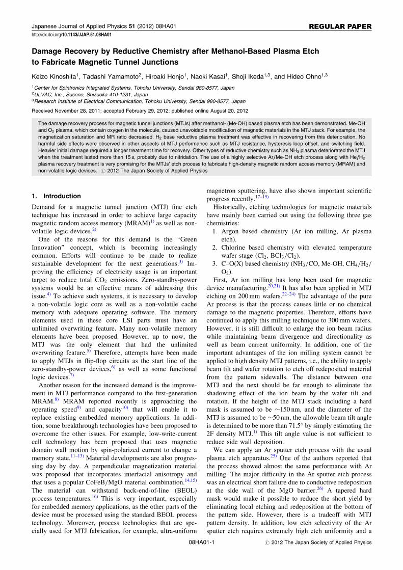
Stack structures used in this study and their pattern bird’seye views are presented in Table I and Fig. 1, respectively.Two types of magnetic stacks were prepared, with the majordifferences between them being in the free layer material.These were (a) CoFeB, and (b) NiFe. All the films had in-plane magnetization. There were slight differences in themetal cap structure (Cap) just above the free layer. The otherparts, i.e., the bottom electrode (BE), pin layer (Pin) tunnelbarrier, top electrode (TE), and hard mask (HM) were thesame. The short axes of these ellipsoidal patterns were0.32 �m on the mask. Their ellipsoid aspect ratios were 3.
The plasma etch/treatment procedure for each stack isgiven in Table II, and the detailed etch/treatment conditionsare in Table III. Dot pattern (a) was fully etched by pure Arplasma, which was expected to cause no damage or at leastless damage than other processes to fabricate a simple dotpattern array over the wafer. After etching, the samples wereintentionally exposed to O2 plasma to partially oxidize thepattern, and then followed by H2 plasma treatment forreduction at 200 �C. An inductively-coupled-plasma (ICP)source was used in these etches and treatments. The plasmatreatment times were varied. After finishing these plasmaprocesses, the chip was directly evaluated using a vibrating-sample magnetometer (VSM). Magnetic field (H) was sweptwith measuring magnetization (M) to obtain a major M–Hhysteresis loop. Magnetization saturation (Ms) was derivedfrom the hysteresis.
MTJ pattern (b) was fabricated in two-layer BEOLinterconnects. Ar/Me-OH plasma was used to etch the freelayer and was stopped over the MgO barrier. Magnetized-ICP (MICP) or ICP source was used for Ar/Me-OH etching.
Table I. Sample stack structures.
Free layer Shape /BE/Pin/Barrier/Free/Cap/TE/HM
(a) CoFeB Dot Si-sub./SiO/Ta/PtMn/CoFe/Ru/CoFeB/MgO/CoFeB/Ta/Ru/Ta/SiN/SiO
(b) NiFe MTJ M4/SiO/Ta/PtMn/CoFe/Ru/CoFeB/MgO/NiFe/Ru/Pt/Ru/Ta/SiN/SiO
(b)(a)
HM
TECapFree
Barrier
HM
TECap
Pin
BE
Free
Fig. 1. (Color online) Dot and MTJ pattern birds eye views fabricated in
this study.
Table II. Etch/treatment procedure.
Free layer Shape Stack etch oxidation Etch end point Reduction treatment
(a) CoFeB Dot Pure Ar etch + O2 plasma exposure Full etch H2 plasma
(b) NiFe MTJ Ar/Me-OH plasma etch Stop over MgO He/H2 or NH3 plasma
K. Kinoshita et al.Jpn. J. Appl. Phys. 51 (2012) 08HA01
08HA01-2 # 2012 The Japan Society of Applied Physics
Bias voltage-peak-to-peak (Vpp) value during the etchingwas 770V for both apparatuses. After etching, the sampleswere treated by He/H2 plasma or NH3 plasma as thereduction treatment under the substrate temperature at 180and 200 �C, respectively. To enhance the reductive reaction,we applied these high temperature conditions. An Ar ionmilling system was also used to obtain reference data of theMTJ. The long axes of the ellipsoidal MTJ patterns were set45� off axis from notch to top direction on the wafer. Detailsof the MTJ fabrication procedure are described elsewhere.26)
The MTJ was evaluated after completing the BEOL processusing an auto-prober under external magnetic field (Hex)conditions. R–H hysteresis loops were obtained by measur-ing MTJ resistance (R) while sweeping the Hex. Thedistribution of magnetoresistive (MR) ratio, MTJ resistance(R), hysteresis offset (Hoff), and switching field (Hsw) werederived from the hysteresis. Cross-sectional transmissionelectron microscopic images were taken after the MTJfabrication. A transmission electron microscopy/electronenergy-loss spectroscopy (TEM–EELS) technique wasapplied to analyze the NiFe layer.
3. Results and Discussion
3.1 Magnetic properties of CoFeB dot by plasma
treatment
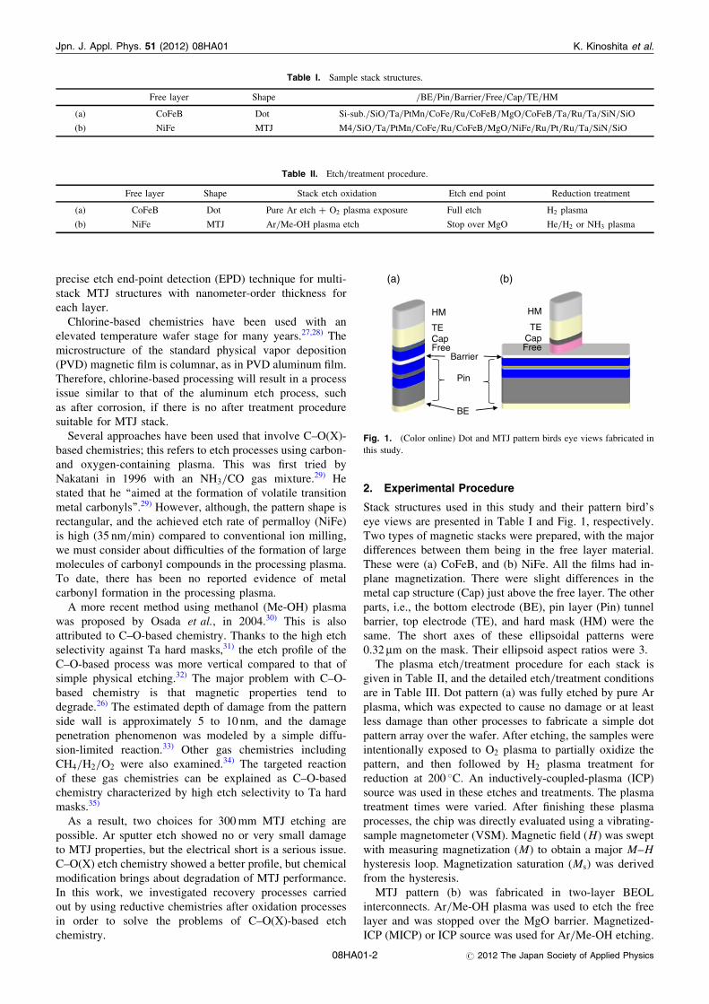
Figure 2(a) shows major M–H hysteresis loops for theCoFeB dot sample taken at each step of the treatments. Thesolid line is the hysteresis of a sample etched by pure Arplasma, which is thought to have the smallest deteriorationof magnetic properties. Here, Ms is one of the importantproperties of the magnetic thin film, which is defined by theheight of M–H hysteresis. After 20 s of O2 plasma exposurefor this sample, the Ms decreased due to oxidation, as shownby the filled square plots on the broken line. Then, asindicated by the open rhomboidal plots on the solid line, theMs recovered to the initial Ar etch level with the H2 plasmatreatment. These results indicate that the degradation of themagnetic property due to oxidation propagated from the sidewall of the dot pattern and that the reductive plasmachemistry recovered the original property. Figure 2(b) plotsM–H hysteresis with varying O2 plasma exposure timesafter Ar sputter etching. The H2 plasma treatment time waskept constant at 200 s. The Ms decreased gradually whilethe O2 exposure time was increased. This implies that themagnitude of the reductive treatment is sufficient to recoverfrom the given oxidation damage.
3.2 Recovery treatment for NiFe MTJ
3.2.1 Effects on MTJ characteristics
The MTJs were prepared by etching them in Ar diluted Me-
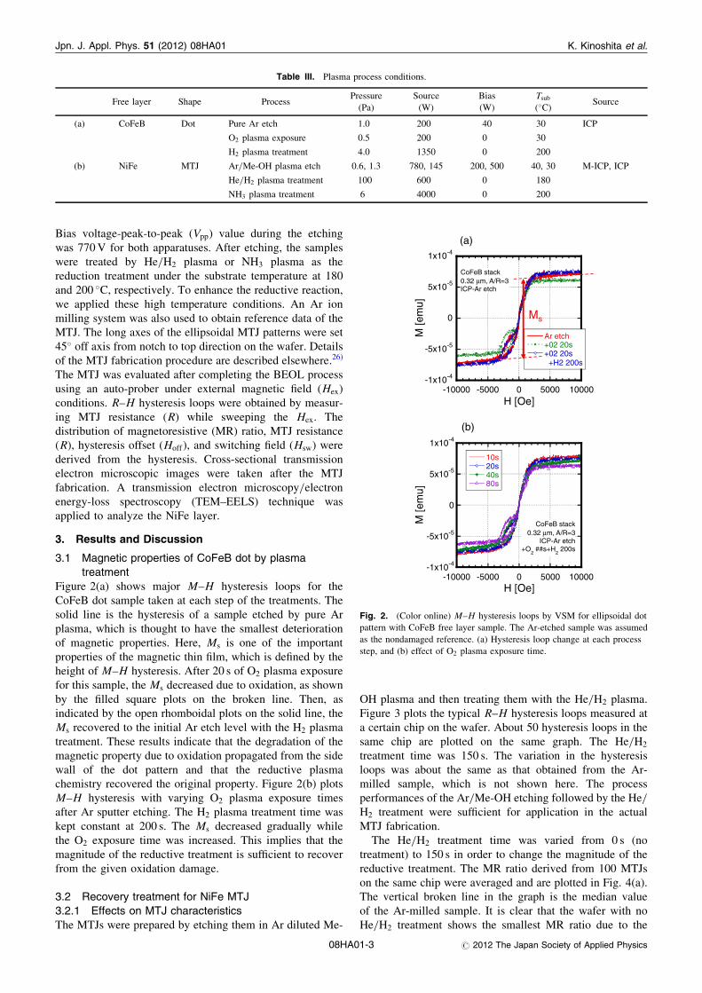
OH plasma and then treating them with the He/H2 plasma.Figure 3 plots the typical R–H hysteresis loops measured ata certain chip on the wafer. About 50 hysteresis loops in thesame chip are plotted on the same graph. The He/H2
treatment time was 150 s. The variation in the hysteresisloops was about the same as that obtained from the Ar-milled sample, which is not shown here. The processperformances of the Ar/Me-OH etching followed by the He/H2 treatment were sufficient for application in the actualMTJ fabrication.
The He/H2 treatment time was varied from 0 s (notreatment) to 150 s in order to change the magnitude of thereductive treatment. The MR ratio derived from 100 MTJson the same chip were averaged and are plotted in Fig. 4(a).The vertical broken line in the graph is the median valueof the Ar-milled sample. It is clear that the wafer with noHe/H2 treatment shows the smallest MR ratio due to the
-1x10⁻⁴
-5x10⁻⁵
0
5x10⁻⁵
1x10⁻⁴
-10000 -5000 0 5000 10000
Ar etch+02 20s+02 20s +H2 200s
CoFeB stack0.32 μm, A/R=3ICP-Ar etch
M [e
mu]
H [Oe]
Ms
(a)
-1x10⁻⁴
-5x10⁻⁵
0
5x10⁻⁵
1x10⁻⁴
-10000 -5000 0 5000 10000
10s20s40s80s
M [e
mu]
H [Oe]
CoFeB stack0.32 μm, A/R=3
ICP-Ar etch+O
2 ##s+H
2 200s
(b)
Fig. 2. (Color online) M–H hysteresis loops by VSM for ellipsoidal dot
pattern with CoFeB free layer sample. The Ar-etched sample was assumed
as the nondamaged reference. (a) Hysteresis loop change at each process
step, and (b) effect of O2 plasma exposure time.
Table III. Plasma process conditions.
Free layer Shape ProcessPressure
(Pa)
Source
(W)
Bias
(W)
Tsub(�C)
Source
(a) CoFeB Dot Pure Ar etch 1.0 200 40 30 ICP
O2 plasma exposure 0.5 200 0 30
H2 plasma treatment 4.0 1350 0 200
(b) NiFe MTJ Ar/Me-OH plasma etch 0.6, 1.3 780, 145 200, 500 40, 30 M-ICP, ICP
He/H2 plasma treatment 100 600 0 180
NH3 plasma treatment 6 4000 0 200
K. Kinoshita et al.Jpn. J. Appl. Phys. 51 (2012) 08HA01
08HA01-3 # 2012 The Japan Society of Applied Physics
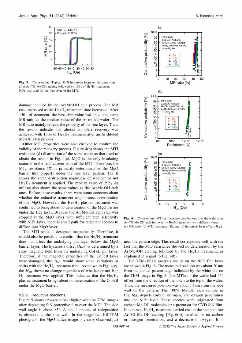
damage induced by the Ar/Me-OH etch process. The MRratio increased as the He/H2 treatment time increased. After150 s of treatment, the best chip value had about the sameMR ratio as the median value of the Ar-milled wafer. TheMR ratio mainly reflects the property of the free layer. Thus,the results indicate that almost complete recovery wasachieved with 150 s of He/H2 treatment after an Ar-dilutedMe-OH etch process.
Other MTJ properties were also checked to confirm thevalidity of the recovery process. Figure 4(b) shows the MTJresistance (R) distribution of the same wafer as that used toobtain the results in Fig. 4(a). MgO is the only insulatingmaterial in the read current path of the MTJ. Therefore, theMTJ resistance (R) is primarily determined by the MgObarrier film property under the free layer pattern. The Rshows the same distribution regardless of whether or notHe/H2 treatment is applied. The median value of R by Armilling also shows the same values as the Ar/Me-OH etchones. Before these results, there were some concerns aboutwhether the reductive treatment might cause deteriorationof the MgO. However, the He/H2 plasma treatment wasconfirmed to bring about no deterioration of the MgO barrierunder the free layer. Because the Ar/Me-OH etch step wasstopped at the MgO layer with sufficient etch selectivitywith NiFe layer, there is small path for reductant species todiffuse into MgO layer.
The MTJ stack is designed magnetically. Therefore, itshould also be possible to confirm that the He/H2 treatmentdoes not affect the underlying pin layer below the MgObarrier layer. The hysteresis offset (Hoff) is determined by astray magnetic field from the underlying CoFeB pin layer.Therefore, if the magnetic properties of the CoFeB layerwere damaged, the Hoff would show some variations orshifts with the He/H2 treatment time. As shown in Fig. 4(c),the Hoff shows no change regardless of whether or not He/H2 treatment was applied. This indicates that the He/H2
plasma treatment brings about no deterioration of the CoFeBunder the MgO barrier.
3.2.2 Reductive reactions
Figure 5 shows cross-sectional high-resolution TEM imagesafter depositing SiN protective film over the MTJ. The sidewall angle is about 85�. A small amount of redepositionis observed at the side wall. In the magnified HR-TEMphotograph, the MgO lattice image is clearly observed just
near the pattern edge. This result corresponds well with thefact that the MTJ resistance showed no deterioration by theAr/Me-OH etching followed by the He/H2 treatment, asexplained in regard to Fig. 4(b).
The TEM–EELS analysis results on the NiFe free layerare shown in Fig. 6. The measured position was about 20 nmfrom the etched pattern edge indicated by the white dot onthe TEM image in Fig. 5. The MTJs on the wafer had 45�
offset from the direction of the notch to the top of the wafer.Thus, the measured position was about 14 nm from the sidewall of the pattern. The 100% Me-OH etch sample inFig. 6(a) depicts carbon, nitrogen, and oxygen penetrationinto the NiFe layer. These species were originated frometchant Me-OH molecules or a precursor for CVD-SiN film.In contrast, He/H2 treatment carried out on the sample afterAr–8% Me-OH etching [Fig. 6(b)] resulted in no carbonor nitrogen penetration, and a decrease in oxygen. It is
(a)
0 10 20 30 40 50.1
1
51020305070809095
99
99.9
0s15s40s150s
MR ratio [%]
Cum
ulat
ive
prob
abili
ty [%
]
NiFe stack0.32 μm, A/R=2.5M-ICP, 100 MTJs/chipAr/Me-OH etch, 0.5 Pa + He/H
2 ##s
Ar
mill
ing
(b)
100 1000 1x10⁴ 1x105.1
1
51020305070809095
99
99.9
0s15s40s150s
Resistance [Ω]C
umul
ativ
e pr
obab
ility
[%]
NiFe stack0.32 μm, A/R=2.5M-ICP, 100 MTJs/chipAr/Me-OH etch, 0.5 Pa + He/H
2 ##s
Ar
mill
ing
-15 -10 -5 0 5 10.1
1
51020305070809095
99
99.9
0s15s40s150s
Hoff
[Oe]
Cum
ulat
ive
prob
abili
ty [%
]
NiFe stack0.32 μm, A/R=2.5M-ICP, 100 MTJs/chipAr/Me-OH etch, 0.5 Pa + He/H
2 ##s
(c)
Fig. 4. (Color online) MTJ performance distributions over the wafer after
Ar–7% Me-OH etch followed by He/H2 treatment with different times:
(a) MR ratio, (b) MTJ resistance (R), and (c) hysteresis loop offset (Hoff ).
0
10
20
30
40
50
60
806040200-20-40-60-80
MR
rat
io [%
]
Hex [Oe]
0.32 μm, A/R=2.5Chip 45, 50 MTJs
Fig. 3. (Color online) Typical R–H hysteresis loops on the same chip
after Ar–7% Me-OH etching followed by 150 s of He/H2 treatment.
NiFe was used for the free layer of the MTJ.
K. Kinoshita et al.Jpn. J. Appl. Phys. 51 (2012) 08HA01
08HA01-4 # 2012 The Japan Society of Applied Physics
presumed that the dilution of the radicals by argon in theetching plasma as well as reductive or cleaning reactionsduring the He/H2 treatment have impacts to reduce thesespecies from the NiFe layer.
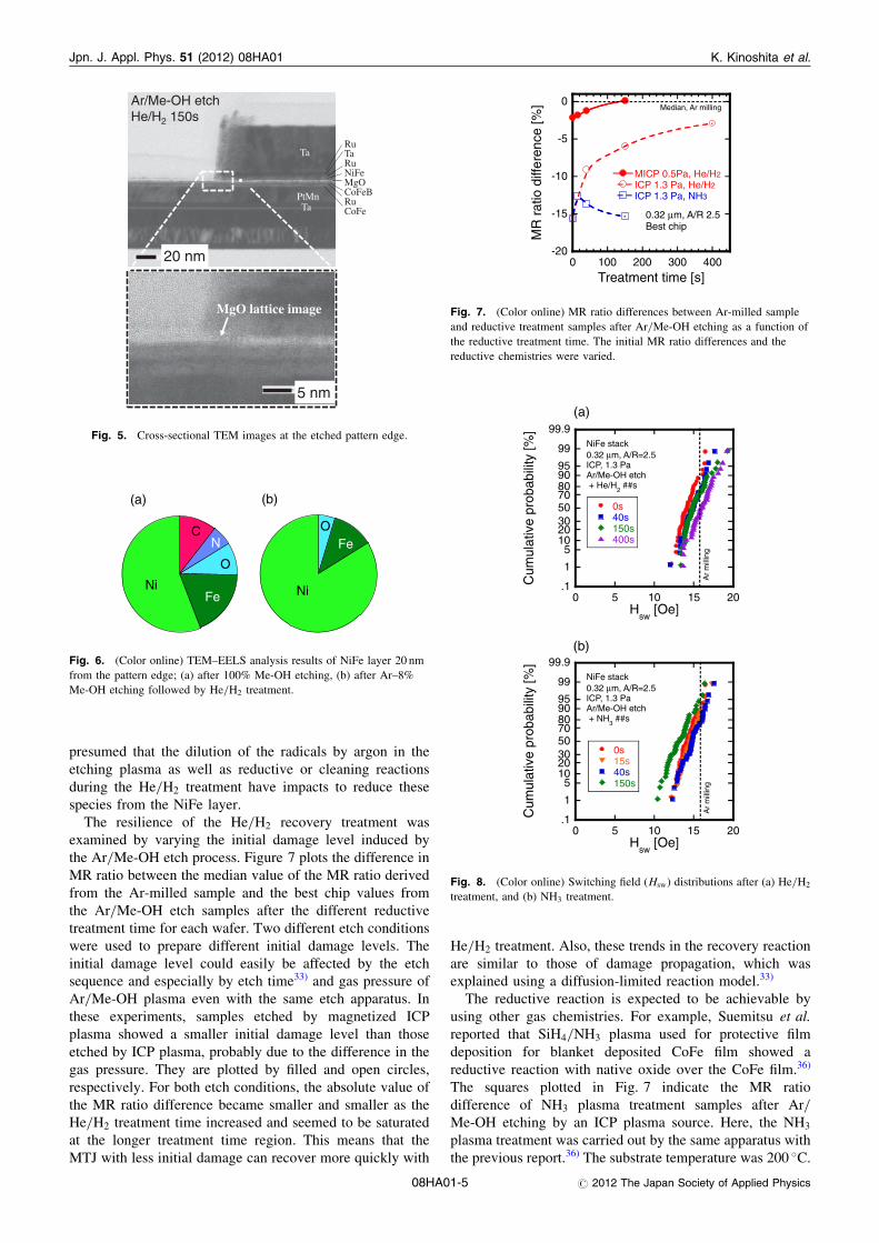
The resilience of the He/H2 recovery treatment wasexamined by varying the initial damage level induced bythe Ar/Me-OH etch process. Figure 7 plots the difference inMR ratio between the median value of the MR ratio derivedfrom the Ar-milled sample and the best chip values fromthe Ar/Me-OH etch samples after the different reductivetreatment time for each wafer. Two different etch conditionswere used to prepare different initial damage levels. Theinitial damage level could easily be affected by the etchsequence and especially by etch time33) and gas pressure ofAr/Me-OH plasma even with the same etch apparatus. Inthese experiments, samples etched by magnetized ICPplasma showed a smaller initial damage level than thoseetched by ICP plasma, probably due to the difference in thegas pressure. They are plotted by filled and open circles,respectively. For both etch conditions, the absolute value ofthe MR ratio difference became smaller and smaller as theHe/H2 treatment time increased and seemed to be saturatedat the longer treatment time region. This means that theMTJ with less initial damage can recover more quickly with
He/H2 treatment. Also, these trends in the recovery reactionare similar to those of damage propagation, which wasexplained using a diffusion-limited reaction model.33)
The reductive reaction is expected to be achievable byusing other gas chemistries. For example, Suemitsu et al.reported that SiH4/NH3 plasma used for protective filmdeposition for blanket deposited CoFe film showed areductive reaction with native oxide over the CoFe film.36)
The squares plotted in Fig. 7 indicate the MR ratiodifference of NH3 plasma treatment samples after Ar/Me-OH etching by an ICP plasma source. Here, the NH3
plasma treatment was carried out by the same apparatus withthe previous report.36) The substrate temperature was 200 �C.
(a)
CN
O
FeNi
(b)
Fe
Ni
O
Fig. 6. (Color online) TEM–EELS analysis results of NiFe layer 20 nm
from the pattern edge; (a) after 100% Me-OH etching, (b) after Ar–8%
Me-OH etching followed by He/H2 treatment.
-20
-15
-10
-5
0
0 100 200 300 400
MICP 0.5Pa, He/H2ICP 1.3 Pa, He/H2ICP 1.3 Pa, NH3
Treatment time [s]
MR
rat
io d
iffer
ence
[%]
0.32 μm, A/R 2.5Best chip
Median, Ar milling
Fig. 7. (Color online) MR ratio differences between Ar-milled sample
and reductive treatment samples after Ar/Me-OH etching as a function of
the reductive treatment time. The initial MR ratio differences and the
reductive chemistries were varied.
TaRuTaRuNiFeMgOCoFeBRuCoFe
PtMnTa
Ar/Me-OH etchHe/H2 150s
MgO lattice image
5 nm
20 nm
Fig. 5. Cross-sectional TEM images at the etched pattern edge.
(a)
0 5 10 15 20.1
1
51020305070809095
99
99.9
0s40s150s400s
Hsw
[Oe]
Cum
ulat
ive
prob
abili
ty [%
]
NiFe stack0.32 μm, A/R=2.5ICP, 1.3 PaAr/Me-OH etch + He/H
2 ##s
Ar
mill
ing
(b)
0 5 10 15 20.1
1
51020305070809095
99
99.9
0s15s40s150s
Hsw
[Oe]
Cum
ulat
ive
prob
abili
ty [%
]
NiFe stack0.32 μm, A/R=2.5ICP, 1.3 PaAr/Me-OH etch + NH
3 ##s
Ar
mill
ing
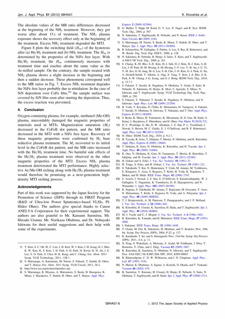
Fig. 8. (Color online) Switching field (Hsw) distributions after (a) He/H2
treatment, and (b) NH3 treatment.
K. Kinoshita et al.Jpn. J. Appl. Phys. 51 (2012) 08HA01
08HA01-5 # 2012 The Japan Society of Applied Physics
The absolute values of the MR ratio differences decreasedat the beginning of the NH3 treatment. However, they gotworse after about 15 s of treatment. The NH3 plasmaexposure shows the recovery effect only at the beginning ofthe treatment. Excess NH3 treatment degraded the MTJ.
Figure 8 plots the switching field (Hsw) of the hysteresisafter (a) He/H2 treatment and (b) NH3 treatment. The Hsw isdetermined by the properties of the NiFe free layer. WithHe/H2 treatment, the Hsw continuously increases withtreatment time and reaches about the same value as theAr-milled sample. On the contrary, the sample treated withNH3 plasma shows a slight increase in the beginning andthen a sudden decrease. These phenomena correspond wellto the MR ratios in Fig. 7. Excess NH3 treatment degradesthe NiFe free layer probably due to nitridation. In the case ofSiN deposition over CoFe film,36) the sample surface wascovered by SiN film soon after starting the deposition. Thus,the excess reaction was prevented.
4. Conclusion
Oxygen-containing plasma, for example, methanol (Me-OH)plasma, unavoidably damaged the magnetic properties ofmaterials used in MTJs. Magnetization saturation (Ms)decreased in the CoFeB dot pattern, and the MR ratiodecreased in the MTJ with a NiFe free layer. Recovery ofthese magnetic properties were confirmed by H2 basereductive plasma treatment. The Ms recovered to its initiallevel in the CoFeB dot pattern, and the MR ratio increasedwith the He/H2 treatment time. No harmful side effects ofthe He/H2 plasma treatment were observed in the othermagnetic properties of the MTJ. Excess NH3 plasmatreatment deteriorated the MTJ performance. Highly selec-tive Ar/Me-OH etching along with He/H2 plasma treatmentwould therefore be promising as a next-generation high-density MTJ etching process.
Acknowledgements
Part of this work was supported by the Japan Society for thePromotion of Science (JSPS) through its FIRST Program(R&D of Ultra-low Power Spintronics-based VLSIs, PI:Hideo Ohno). The authors give special thanks to CanonANELVA Corporation for their experimental support. Theauthors are also grateful to Mr. Katsumi Suemitsu, Mr.Hiroaki Utsumi, Mr. Norikazu Ohshima, and Dr. NobuyukiIshiwata for their useful suggestions and their help withsome of the experiments.
1) Y. Kim, S. C. Oh, W. C. Lim, J. H. Kim, W. J. Kim, J. H. Jeong, H. J. Shin,
K. W. Kim, K. S. Kim, J. H. Park, S. H. Park, H. Kwon, K. H. Ah, J. E.
Lee, S. O. Park, S. Choi, H. K. Kang, and C. Chung: Ext. Abstr. 2011
Symp. VLSI Technology, 2011, 11B-1.
2) S. Matsunaga, A. Katsumata, M. Natsui, S. Fukami, T. Endoh, H. Ohno,
and T. Hanyu: Ext. Abstr. 2011 Symp. VLSI Circuit, 2011, 28-2.
3) http://www.iea.org/techno/etp/index.asp
4) S. Matsunaga, K. Hiyama, A. Matsumoto, S. Ikeda, H. Hasegawa, K.
Miura, J. Hayakawa, T. Endoh, H. Ohno, and T. Hanyu: Appl. Phys.
Express 2 (2009) 023004.
5) G. Muller, T. Happ, M. Kund, G. Y. Lee, N. Nagel, and R. Sezi: IEDM
Tech. Dig., 2004, p. 567.
6) N. Sakimura, T. Sugibayashi, R. Nebashi, and N. Kasai: IEEE J. Solid-
State Circuits 44 (2009) 2244.
7) S. Matsunaga, M. Natsui, S. Ikeda, K. Miura, T. Endoh, H. Ohno, and T.
Hanyu: Jpn. J. Appl. Phys. 50 (2011) 063004.
8) R. Scheuerlein, W. Gallagher, S. Parkin, A. Lee, S. Ray, R. Robertazzi, and
W. Reohr: Dig. Tech. Pap. ISSCC, 2000, p. 128.
9) N. Sakimura, R. Nebashi, H. Honjo, S. Saito, Y. Kato, and T. Sugibayashi:
A-SSCC’08 Tech. Dig., 2008, p. 261.
10) S. Chung, K.-M. Rho, S.-D. Kim, H.-J. Suh, D.-J. Kim, H.-J. Kim, S.-H.
Lee, J.-H. Park, H.-M. Hwang, S.-M. Hwang, J.-Y. Lee, Y.-B. An, J.-U. Yi,
Y.-H. Seo, D.-H. Jung, M.-S. Lee, S.-H. Cho, J.-N. Kim, G.-J. Park, G. Jin,
A. Driskill-Smith, V. Nikitin, A. Ong, X. Tang, Y. Kim, J.-S. Rho, S.-K.
Park, S.-W. Chung, J.-G. Jeong, and S.-J. Hong: IEDM Tech. Dig., 2010,
p. 12.7.1.
11) S. Fukami, T. Suzuki, K. Nagahara, N. Ohshima, Y. Ozaki, S. Saito, R.
Nebashi, N. Sakimura, H. Honjo, K. Mori, C. Igarashi, S. Miura, N.
Ishiwata, and T. Sugibayashi: Symp. VLSI Technology Dig. Tech. Pap.,
2009, p. 230.
12) S. Fukami, Y. Nakatani, T. Suzuki, K. Nagahara, N. Ohshima, and N.
Ishiwata: Appl. Phys. Lett. 95 (2009) 232504.
13) K. Ueda, T. Koyama, D. Chiba, K. Shimamura, H. Tanigawa, S. Fukami,
T. Suzuki, N. Ohshima, N. Ishiwata, Y. Nakatani, and T. Ono: Appl. Phys.
Express 4 (2011) 063003.
14) S. Ikeda, K. Miura, H. Yamamoto, K. Mizunuma, H. D. Gan, M. Endo, S.
Kanai, J. Hayakawa, F. Matsukura, and H. Ohno: Nat. Mater. 9 (2010) 721.
15) D. C. Worledge, G. Hu, D. W. Abraham, J. Z. Sun, P. L. Trouilloud, J.
Nowak, S. Brown, M. C. Gaidis, E. J. O’Sullivan, and R. P. Robertazzi:
Appl. Phys. Lett. 98 (2011) 022501.
16) H. Ohno: IEDM Tech. Dig., 2010, p. 9.2.1.
17) H. Toyoda, K. Goto, T. Ishijima, T. Morita, N. Ohshima, and K. Kinoshita:
Appl. Phys. Express 2 (2009) 126001.
18) T. Ishijima, K. Goto, N. Ohshima, K. Kinoshita, and H. Toyoda: Jpn. J.
Appl. Phys. 48 (2009) 116004.
19) K. Ono, N. Ohshima, K. Goto, H. Yamamoto, T. Morita, K. Kinoshita, T.
Ishijima, and H. Toyoda: Jpn. J. Appl. Phys. 50 (2011) 023001.
20) H. Gokan and S. Esho: J. Vac. Sci. Technol. 18 (1981) 23.
21) H. Tsuge, S. Esho, and H. Gokan: J. Vac. Sci. Technol. 19 (1981) 221.
22) S. Takahashi, T. Kai, N. Shimomura, T. Ueda, M. Amano, M. Yoshikawa,
E. Kitagawa, Y. Asao, S. Ikegawa, T. Kishi, H. Yoda, K. Nagahara, T.
Mukai, and H. Hada: IEEE Trans. Magn. 42 (2006) 2745.
23) S. Assefa, J. Nowak, J. Z. Sun, E. O’Sullivan, S. Kanakasabapathy, W. J.
Gallagher, Y. Nagamine, K. Tsunekawa, D. D. Djayaprawira, and N.
Watanabe: J. Appl. Phys. 102 (2007) 063901.
24) K. Sugiura, S. Takahashi, M. Amano, T. Kajiyama, M. Iwayama, Y. Asao,
N. Shimomura, T. Kishi, S. Ikegawa, H. Yoda, and A. Nitayama: Jpn. J.
Appl. Phys. 48 (2009) 08HD02.
25) T. J. Kropewnicki, A. M. Paterson, T. Panagopoulos, and J. P. Holland:
J. Vac. Sci. Technol. A 24 (2006) 444.
26) K. Kinoshita, H. Utsumi, K. Suemitsu, H. Hada, and T. Sugibayashi: Jpn. J.
Appl. Phys. 49 (2010) 08JB02.
27) M. J. Vasile and C. J. Mogab: J. Vac. Sci. Technol. A 4 (1986) 1841.
28) K. Kinoshita, K. Yamada, and H. Matsutera: IEEE Trans. Magn. 27 (1991)
4888.
29) I. Nakatani: IEEE Trans. Magn. 32 (1996) 4448.
30) T. Osada, M. Doi, K. Sakamoto, H. Maehara, and Y. Kodaira: Proc. 26th
Int. Symp. Dry Process (DPS), 2004, P-22, p. 127.
31) K. Karahashi, T. Ito, and S. Hamaguchi: Proc. 33rd Int. Symp. Dry Process
(DPS), 2011, A-6, p. 11.
32) X. Peng, S. Wakeham, A. Morrone, S. Axdal, M. Feldbaum, J. Hwu, T.
Boonstra, Y. Chen, and J. Ding: Vacuum 83 (2009) 1007.
33) K. Kinoshita, K. Suemitsu, N. Ohshima, N. Ishiwata, and T. Sugibayashi:
Proc. 63rd GEC/7th ICRP/28th SPP, 2010, KWP-00067.
34) B. Khamsehpour, C. D. W. Wilkinson, and J. N. Chapman: Appl. Phys.
Lett. 67 (1995) 3194.
35) N. Matsui, K. Mashimo, A. Egami, A. Konishi, O. Okada, and T. Tsukada:
Vacuum 66 (2002) 479.
36) K. Suemitsu, Y. Kawano, H. Utsumi, H. Honjo, R. Nebashi, S. Saito, N.
Ohshima, T. Sugibayashi, and H. Hada: Jpn. J. Appl. Phys. 47 (2008) 2714.
K. Kinoshita et al.Jpn. J. Appl. Phys. 51 (2012) 08HA01
08HA01-6 # 2012 The Japan Society of Applied Physics


