Embed Size (px)
Citation preview
User Manual
DA14531 USB Development Kit Hardware
UM-B-125
Abstract
This document outlines the system design, configuration options, and supported features of DA14531 USB Development Kit revC/D (376-13-C or D).
UM-B-125
DA14531 USB Development Kit Hardware
User Manual Revision 1.2 18-March-2022
CFR0012 2 of 33 © 2022 Dialog Semiconductor
Contents
Abstract ................................................................................................................................................ 1
1 Terms and Definitions ................................................................................................................... 4
2 References ..................................................................................................................................... 4
3 Introduction.................................................................................................................................... 5
4 System Overview ........................................................................................................................... 5
4.1 Features ................................................................................................................................ 5
4.2 System and Components Description (Top View) ................................................................ 6
4.3 System and Components Description (Bottom View) ........................................................... 7
5 USB Kit System ............................................................................................................................. 8
5.1 Overview ............................................................................................................................... 8
5.2 DA14531 System .................................................................................................................. 9
5.3 DA14531 GPIO Assignment ............................................................................................... 10
5.4 Default Configuration .......................................................................................................... 11
5.5 1-wire Bootable UART ........................................................................................................ 12
5.6 Optional 2-/4-Wire UART .................................................................................................... 13
5.7 Crystals ............................................................................................................................... 14
5.8 Antenna and RF Port .......................................................................................................... 15
5.9 SPI Data Flash Memory (U2) .............................................................................................. 16
5.10 Reset Circuit ........................................................................................................................ 17
5.11 General Purpose Push Button ............................................................................................ 18
5.12 Debugging Port DIP Switch ................................................................................................ 19
5.13 MikroBUS™ Module ............................................................................................................ 20
5.14 User Controlled LED ........................................................................................................... 21
5.15 GND Test Point ................................................................................................................... 21
5.16 Over Voltage Protection Circuit (OVP) ................................................................................ 22
5.17 Debug Interface (U4) ........................................................................................................... 23
5.18 Power Measurements ......................................................................................................... 24
5.19 Operation from a Wall Adapter or Power Pack ................................................................... 25
5.20 Operation from a Coin Cell Battery ..................................................................................... 26
5.21 Known Issues ...................................................................................................................... 26
Appendix A Schematics .................................................................................................................... 27
Appendix B Components Placement on PCB ................................................................................ 29
Appendix C PCB Layer Chart ........................................................................................................... 30
Appendix D PCBA label .................................................................................................................... 31
Revision History ................................................................................................................................ 32
UM-B-125
DA14531 USB Development Kit Hardware
User Manual Revision 1.2 18-March-2022
CFR0012 3 of 33 © 2022 Dialog Semiconductor
Figures
Figure 1: DA14531 USB Kit ................................................................................................................... 5 Figure 2: USB Kit - Top Side ................................................................................................................. 6 Figure 3: USB Kit - Bottom Side ............................................................................................................ 7 Figure 4: Block diagram of DA14531 USB Development Kit ................................................................ 9 Figure 5: DA14531 Section Schematic ................................................................................................. 9 Figure 6: Default DIP Switch Configuration ......................................................................................... 11 Figure 7: Single Pin UART Multiplexer ................................................................................................ 12 Figure 8: DIP Switch Configuration for UART ..................................................................................... 13 Figure 9: RF Section ............................................................................................................................ 15 Figure 10: SPI Data Flash ................................................................................................................... 16 Figure 11: SPI Flash Package Options ............................................................................................... 16 Figure 12: Reset Circuit ....................................................................................................................... 17 Figure 13: RESET Push Button (SW1) ............................................................................................... 17 Figure 14: General Purpose Push Button ........................................................................................... 18 Figure 15: General Purpose Push Button SW2................................................................................... 18 Figure 16: DIP Switch Configuration ................................................................................................... 19 Figure 17: MikroBus™ Pin Assignment ............................................................................................... 20 Figure 18: Guides for Proper MikroBus™ Click Board Insertion ......................................................... 20 Figure 19: MikroBus™ Pin Assignment (Bottom View) ....................................................................... 21 Figure 20: General Purpose LED ........................................................................................................ 21 Figure 21: GND Support Point............................................................................................................. 21 Figure 22: Over Voltage Protection Circuit .......................................................................................... 22 Figure 23: Debugging Processor - UART and JTAG Interface (U4) ................................................... 23 Figure 24: Power Measurement Header ............................................................................................. 24 Figure 25: Current Measurement Header (J2) .................................................................................... 24 Figure 26: Operation with a Battery Pack ............................................................................................ 25 Figure 27: Resistor R48 ....................................................................................................................... 25 Figure 28: Resistors R50 and R51 ...................................................................................................... 26 Figure 29: Wrong Label on MikroBus™ Pin Assignment (Bottom View) ............................................ 26 Figure 30: DA14531 SoC and Peripherals .......................................................................................... 27 Figure 31: Debug Interface (UART/JTAG) .......................................................................................... 28 Figure 32: Components Placement, Top Side on the Left and Bottom Side on the Right .................. 29 Figure 33: PCB Cross Section ............................................................................................................ 30 Figure 34: Label on PCBA ................................................................................................................... 31
Tables
Table 1: DA14531 USB Development Kit Pin Assignment ................................................................. 10 Table 2: Default Configuration DIP Settings........................................................................................ 11 Table 3: UART Configuration DIP Settings ......................................................................................... 13 Table 4: Y1 (32 MHz Crystal) Characteristics ..................................................................................... 14 Table 5: Y2 (32 kHz Crystal) Characteristics ...................................................................................... 14 Table 6: RF Components Names and Values ..................................................................................... 15 Table 7: DIP Switch Configuration ...................................................................................................... 19 Table 8: Information provided on PCBA label ..................................................................................... 31 Table 9: Date code vs SPI Flash ......................................................................................................... 31
UM-B-125
DA14531 USB Development Kit Hardware
User Manual Revision 1.2 18-March-2022
CFR0012 4 of 33 © 2022 Dialog Semiconductor
1 Terms and Definitions
CIB Communication Interface Board
DCR Direct Current Resistor
DMIPS Dhrystone Million Instructions per Second
ESR Effective Series Resistance
GPIO General Purpose Input Output
I2C Inter-Integrated Circuit
JTAG Join Test Action Group
LDO Low Dropout
MISO Master In Slave Out
MOSI Master Out Slave In
OTP One Time Programmable
OVP Over Voltage Protection
PC Personal Computer
PCB Printed Circuit Board
PCBA Printed Circuit Board Assembly
PLL Phase-Locked Loop
QSPI Quad Serial Peripheral Interface
RF Radio Frequency
RFIO Radio Frequency Input Output
SDK Software Development Kit
SIMO Single-Inductor Multiple-Output
SMA Sub-Miniature version A
SMD Surface-Mount Device
SoC System on Chip
SOIC Small Outline Integrated Circuit
SPI Serial Peripheral Interface
SW Software
UART Universal Asynchronous Receiver-Transmitter
USB Universal Serial Bus
2 References
[1] DA14531, Datasheet, Dialog Semiconductor.
[2] AN-B-052, DA1458x/68x Development kit J-Link Interface, Application Note, Dialog Semiconductor.
[3] AN-B-072, DA14531 Booting Options, Application Note, Dialog Semiconductor.
[4] AN-B-027, Designing Printed Antennas for Bluetooth Smart, Application Note, Dialog Semiconductor.
UM-B-125
DA14531 USB Development Kit Hardware
User Manual Revision 1.2 18-March-2022
CFR0012 5 of 33 © 2022 Dialog Semiconductor
3 Introduction
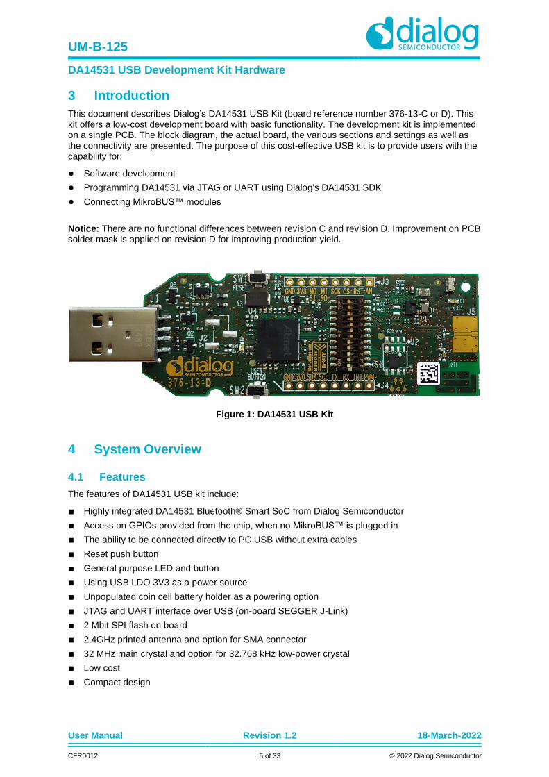
This document describes Dialog’s DA14531 USB Kit (board reference number 376-13-C or D). This kit offers a low-cost development board with basic functionality. The development kit is implemented on a single PCB. The block diagram, the actual board, the various sections and settings as well as the connectivity are presented. The purpose of this cost-effective USB kit is to provide users with the capability for:
Software development
Programming DA14531 via JTAG or UART using Dialog's DA14531 SDK
Connecting MikroBUS™ modules
Notice: There are no functional differences between revision C and revision D. Improvement on PCB solder mask is applied on revision D for improving production yield.
Figure 1: DA14531 USB Kit
4 System Overview
4.1 Features
The features of DA14531 USB kit include:
Highly integrated DA14531 Bluetooth® Smart SoC from Dialog Semiconductor
Access on GPIOs provided from the chip, when no MikroBUS™ is plugged in
The ability to be connected directly to PC USB without extra cables
Reset push button
General purpose LED and button
Using USB LDO 3V3 as a power source
Unpopulated coin cell battery holder as a powering option
JTAG and UART interface over USB (on-board SEGGER J-Link)
2 Mbit SPI flash on board
2.4GHz printed antenna and option for SMA connector
32 MHz main crystal and option for 32.768 kHz low-power crystal
Low cost
Compact design
UM-B-125
DA14531 USB Development Kit Hardware
User Manual Revision 1.2 18-March-2022
CFR0012 6 of 33 © 2022 Dialog Semiconductor
4.2 System and Components Description (Top View)
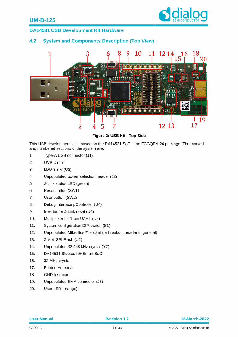
Figure 2: USB Kit - Top Side
This USB development kit is based on the DA14531 SoC in an FCGQFN-24 package. The marked and numbered sections of the system are:
1. Type-A USB connector (J1)
2. OVP Circuit
3. LDO 3.3 V (U3)
4. Unpopulated power selection header (J2)
5. J-Link status LED (green)
6. Reset button (SW1)
7. User button (SW2)
8. Debug interface μController (U4)
9. Inverter for J-Link reset (U6)
10. Multiplexer for 1-pin UART (U5)
11. System configuration DIP-switch (S1)
12. Unpopulated MikroBus™ socket (or breakout header in general)
13. 2 Mbit SPI Flash (U2)
14. Unpopulated 32.468 kHz crystal (Y2)
15. DA14531 Bluetooth® Smart SoC
16. 32 MHz crystal
17. Printed Antenna
18. GND test-point
19. Unpopulated SMA connector (J5)
20. User LED (orange)
UM-B-125
DA14531 USB Development Kit Hardware
User Manual Revision 1.2 18-March-2022
CFR0012 7 of 33 © 2022 Dialog Semiconductor
4.3 System and Components Description (Bottom View)
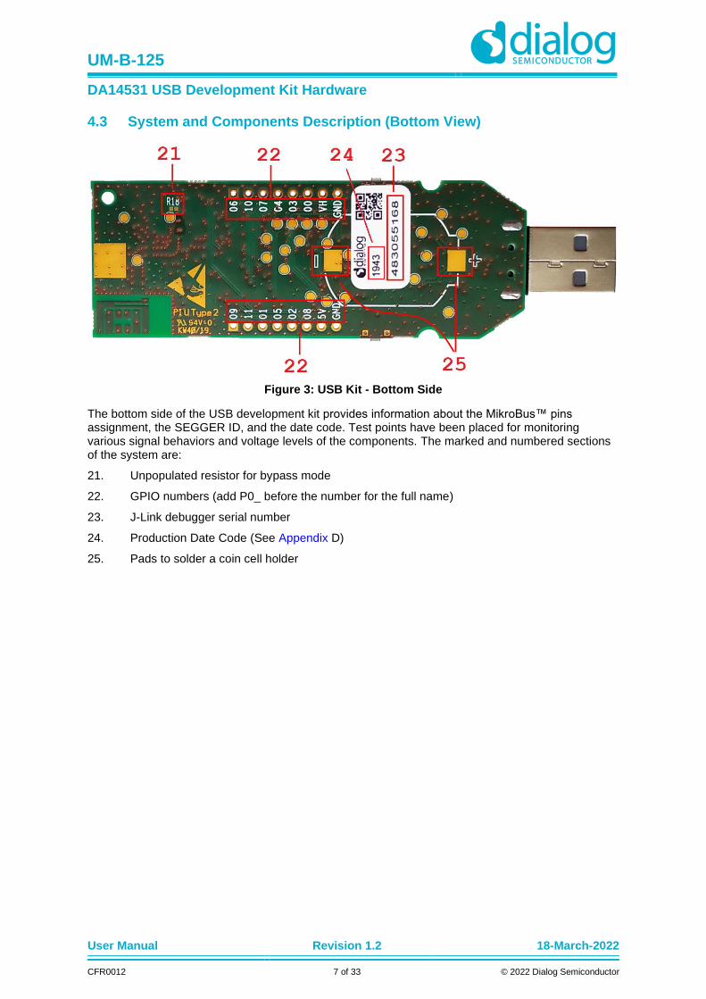
Figure 3: USB Kit - Bottom Side
The bottom side of the USB development kit provides information about the MikroBus™ pins assignment, the SEGGER ID, and the date code. Test points have been placed for monitoring various signal behaviors and voltage levels of the components. The marked and numbered sections of the system are:
21. Unpopulated resistor for bypass mode
22. GPIO numbers (add P0_ before the number for the full name)
23. J-Link debugger serial number
24. Production Date Code (See Appendix D)
25. Pads to solder a coin cell holder
UM-B-125
DA14531 USB Development Kit Hardware
User Manual Revision 1.2 18-March-2022
CFR0012 8 of 33 © 2022 Dialog Semiconductor
5 USB Kit System
5.1 Overview
Board name/number:
DA14531 USB development kit/376-13-C or D
SoC:
DA14531 in FCGQFN-24 package
Flash memory:
AT25DF021A (or MX25R2035F), 2 Mbit, QSPI Flash Memory in 8-pin U-SON (2 mm × 3 mm) package. Note that it is accessed in plain SPI mode.
3.3 V power supply (VHIGH)
Clock inputs:
32 MHz crystal
Optional low power 32.768 kHz crystal
Power
3.3 V LDO powering VHIGH on DA14531 (buck mode configuration)
Ports:
USB port for debugging purposes
Interfaces:
UART-J-Link CDC UART Port (listed under Ports in Device Manager)
JTAG-J-Link Driver (listed under Universal Serial Bus Controllers in Device Manager)
DIP switch to select between interfaces and isolate the signals for accurate power measurements
Connectivity expansion connectors:
One MikroBUS™ module can be plugged to J3/J4. Note that most GPIOs are already used for booting and debugging, so compatibility with any random Click™ board is not guaranteed
UM-B-125
DA14531 USB Development Kit Hardware
User Manual Revision 1.2 18-March-2022
CFR0012 9 of 33 © 2022 Dialog Semiconductor
5.2 DA14531 System
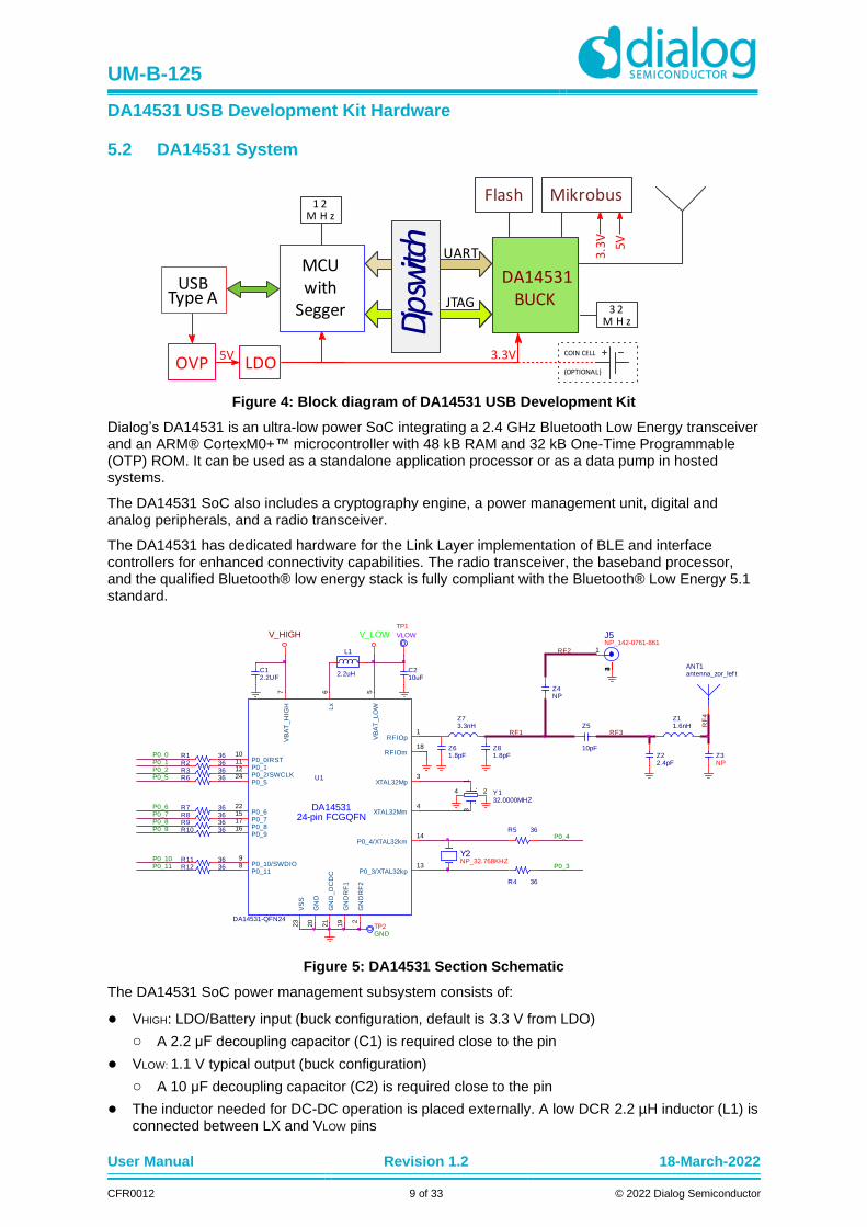
Figure 4: Block diagram of DA14531 USB Development Kit
Dialog’s DA14531 is an ultra-low power SoC integrating a 2.4 GHz Bluetooth Low Energy transceiver and an ARM® CortexM0+™ microcontroller with 48 kB RAM and 32 kB One-Time Programmable (OTP) ROM. It can be used as a standalone application processor or as a data pump in hosted systems.
The DA14531 SoC also includes a cryptography engine, a power management unit, digital and analog peripherals, and a radio transceiver.
The DA14531 has dedicated hardware for the Link Layer implementation of BLE and interface controllers for enhanced connectivity capabilities. The radio transceiver, the baseband processor, and the qualified Bluetooth® low energy stack is fully compliant with the Bluetooth® Low Energy 5.1 standard.
Figure 5: DA14531 Section Schematic
The DA14531 SoC power management subsystem consists of:
VHIGH: LDO/Battery input (buck configuration, default is 3.3 V from LDO)
A 2.2 μF decoupling capacitor (C1) is required close to the pin
VLOW: 1.1 V typical output (buck configuration)
A 10 μF decoupling capacitor (C2) is required close to the pin
The inductor needed for DC-DC operation is placed externally. A low DCR 2.2 µH inductor (L1) is connected between LX and VLOW pins
C210uF
C12.2UF
L1
2.2uH
Z81.8pF
RF1
J5NP_142-0761-861
1
234
Z4NP
RF
4
Z22.4pF
Z5
10pF
Y132.0000MHZ
13
24
Z11.6nH
Z3NP
RF3
ANT1antenna_zor_lef t
Y2NP_32.768KHZ
V_HIGH
DA1453124-pin FCGQFN
U1
DA14531-QFN24
XTAL32Mm4
RFIOm18
RFIOp1
GN
D_
DC
DC
21
XTAL32Mp3
P0_817
P0_111 P0_0/RST10
P0_2/SWCLK12
P0_3/XTAL32kp13
P0_118
GN
D20
GN
DR
F2
2
P0_4/XTAL32km14
P0_524
P0_10/SWDIO9
P0_715 P0_622
Lx
6
VB
AT
_LO
W5
VS
S23
VB
AT
_H
IGH
7
GN
DR
F1
19
P0_916
V_LOW
RF2
P0_1P0_0
P0_8P0_7P0_6
P0_5P0_2
P0_11P0_10
P0_9
P0_3
P0_4R5 36
R4 36
R1 36R2 36
R6 36R3 36
R12 36R11 36
R8 36R7 36
R10 36R9 36
TP1
VLOW
TP2GND
Z61.8pF
Z73.3nH
UM-B-125
DA14531 USB Development Kit Hardware
User Manual Revision 1.2 18-March-2022
CFR0012 10 of 33 © 2022 Dialog Semiconductor
5.3 DA14531 GPIO Assignment
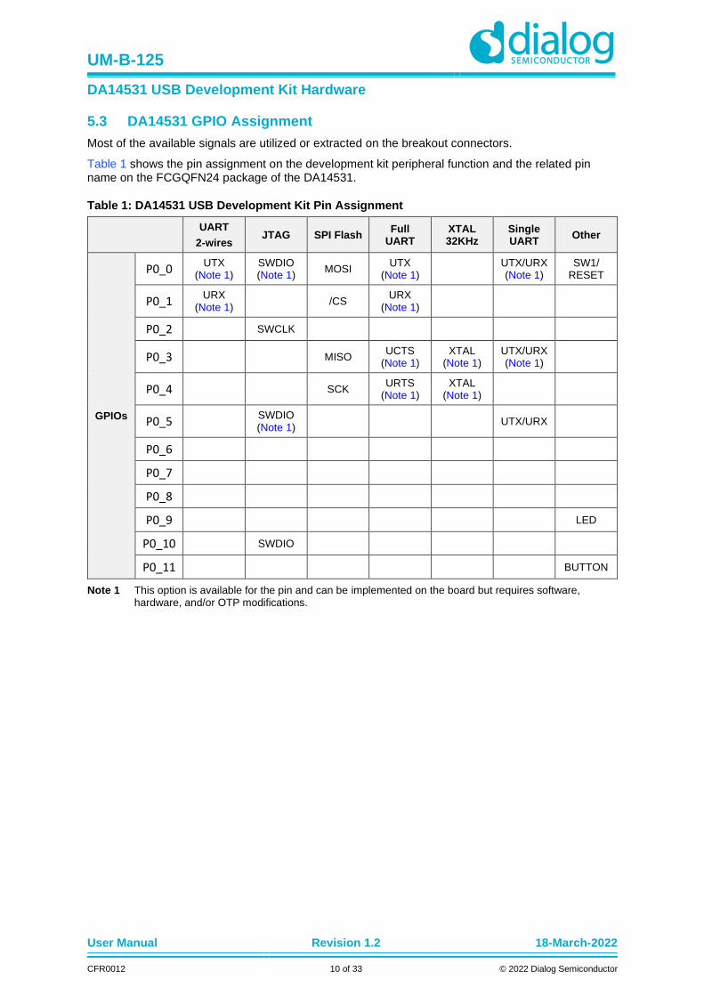
Most of the available signals are utilized or extracted on the breakout connectors.
Table 1 shows the pin assignment on the development kit peripheral function and the related pin name on the FCGQFN24 package of the DA14531.
Table 1: DA14531 USB Development Kit Pin Assignment
UART
2-wires JTAG SPI Flash
Full UART
XTAL 32KHz
Single UART
Other
GPIOs
P0_0 UTX
(Note 1) SWDIO (Note 1)
MOSI UTX
(Note 1)
UTX/URX (Note 1)
SW1/ RESET
P0_1 URX
(Note 1) /CS
URX (Note 1)
P0_2 SWCLK
P0_3 MISO UCTS
(Note 1) XTAL
(Note 1) UTX/URX (Note 1)
P0_4 SCK URTS
(Note 1) XTAL
(Note 1)
P0_5 SWDIO (Note 1)
UTX/URX
P0_6
P0_7
P0_8
P0_9 LED
P0_10 SWDIO
P0_11 BUTTON
Note 1 This option is available for the pin and can be implemented on the board but requires software, hardware, and/or OTP modifications.
UM-B-125
DA14531 USB Development Kit Hardware
User Manual Revision 1.2 18-March-2022
CFR0012 11 of 33 © 2022 Dialog Semiconductor
5.4 Default Configuration
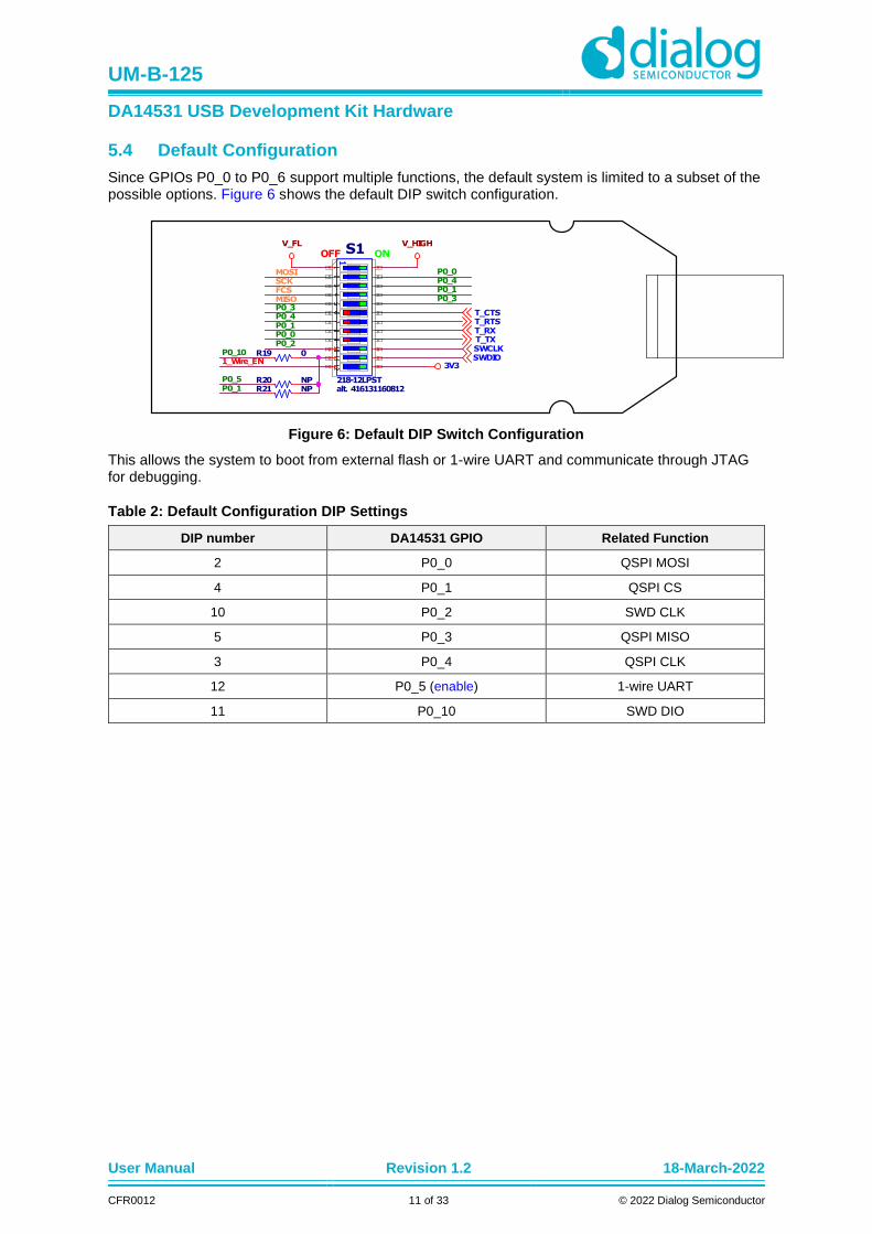
Since GPIOs P0_0 to P0_6 support multiple functions, the default system is limited to a subset of the possible options. Figure 6 shows the default DIP switch configuration.
Figure 6: Default DIP Switch Configuration
This allows the system to boot from external flash or 1-wire UART and communicate through JTAG for debugging.
Table 2: Default Configuration DIP Settings
DIP number DA14531 GPIO Related Function
2 P0_0 QSPI MOSI
4 P0_1 QSPI CS
10 P0_2 SWD CLK
5 P0_3 QSPI MISO
3 P0_4 QSPI CLK
12 P0_5 (enable) 1-wire UART
11 P0_10 SWD DIO
UM-B-125
DA14531 USB Development Kit Hardware
User Manual Revision 1.2 18-March-2022
CFR0012 12 of 33 © 2022 Dialog Semiconductor
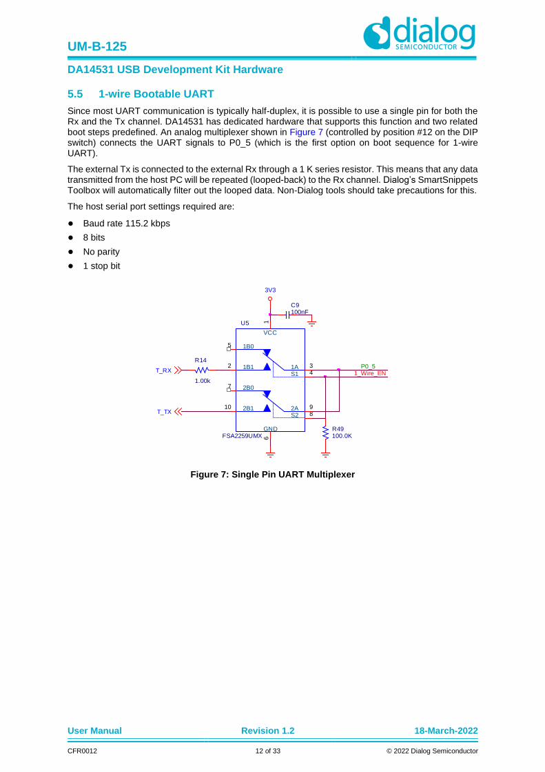
5.5 1-wire Bootable UART
Since most UART communication is typically half-duplex, it is possible to use a single pin for both the Rx and the Tx channel. DA14531 has dedicated hardware that supports this function and two related boot steps predefined. An analog multiplexer shown in Figure 7 (controlled by position #12 on the DIP switch) connects the UART signals to P0_5 (which is the first option on boot sequence for 1-wire UART).
The external Tx is connected to the external Rx through a 1 K series resistor. This means that any data transmitted from the host PC will be repeated (looped-back) to the Rx channel. Dialog’s SmartSnippets Toolbox will automatically filter out the looped data. Non-Dialog tools should take precautions for this.
The host serial port settings required are:
Baud rate 115.2 kbps
8 bits
No parity
1 stop bit
Figure 7: Single Pin UART Multiplexer
C9100nF
P0_5
U5
FSA2259UMX
5 1B0
2 1B14S1
31A
8S2
7 2B0
92A10 2B1
1
VCC
6
GND
R14
1.00k
T_TX
T_RX
R49100.0K
1_Wire_EN
3V3
UM-B-125
DA14531 USB Development Kit Hardware
User Manual Revision 1.2 18-March-2022
CFR0012 13 of 33 © 2022 Dialog Semiconductor
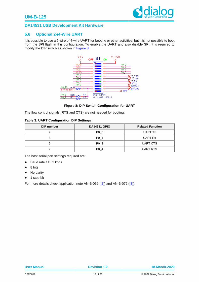
5.6 Optional 2-/4-Wire UART
It is possible to use a 2-wire of 4-wire UART for booting or other activities, but it is not possible to boot from the SPI flash in this configuration. To enable the UART and also disable SPI, it is required to modify the DIP switch as shown in Figure 8.
Figure 8: DIP Switch Configuration for UART
The flow control signals (RTS and CTS) are not needed for booting.
Table 3: UART Configuration DIP Settings
DIP number DA14531 GPIO Related Function
9 P0_0 UART Tx
8 P0_1 UART Rx
6 P0_3 UART CTS
7 P0_4 UART RTS
The host serial port settings required are:
Baud rate 115.2 kbps
8 bits
No parity
1 stop bit
For more details check application note AN-B-052 ([2]) and AN-B-072 ([3]).
UM-B-125
DA14531 USB Development Kit Hardware
User Manual Revision 1.2 18-March-2022
CFR0012 14 of 33 © 2022 Dialog Semiconductor
5.7 Crystals
The DA14531 SoC has two Digitally Controlled Crystal Oscillators, one at 32 MHz (XTAL32M) and the other at 32.768 kHz (XTAL32K). XTAL32K has no trimming capabilities and is used as the clock for low power sleep modes, while XTAL32M can be trimmed.
XTAL32K is by default left unpopulated, because it `cannot be used together with an SPI flash connected to the same GPIOs. The internal RCX low power oscillator is capable to operate with reasonable accuracy in most practical cases. XTAL32K may be required for applications that need to have higher accuracy in low power clock timekeeping or as the source for a Real Time Clock. In that case the crystal can be populated but the on-board flash will not be usable as a boot device. The firmware in that case can reside on the OTP memory. Using external flash at different pins as boot device is also possible with the use of a suitable bootloader in OTP memory.
The crystals selected for the basic development kit are specified in Table 4 and Table 5.
Table 4: Y1 (32 MHz Crystal) Characteristics
Reference Designator Value
Part Number XRCGB32M000F1H00R0
Frequency 32 MHz
Accuracy ±10 ppm
Load Capacitance (CL) 6 pF
Equivalent Series Resistance (ESR) 60 Ω
Drive Level (PD) 150 μW
Table 5: Y2 (32 kHz Crystal) Characteristics
Reference Designator Value
Part Number SC20S-7PF20PPM
Frequency 32.768 KHz
Accuracy ±20 ppm
Load Capacitance (CL) 7 pF
Shunt Capacitance (C0) 1.3 pF
Motional Resistance (ESR) 70 kΩ max
Drive Level (PD) 0.1 μW max
UM-B-125
DA14531 USB Development Kit Hardware
User Manual Revision 1.2 18-March-2022
CFR0012 15 of 33 © 2022 Dialog Semiconductor
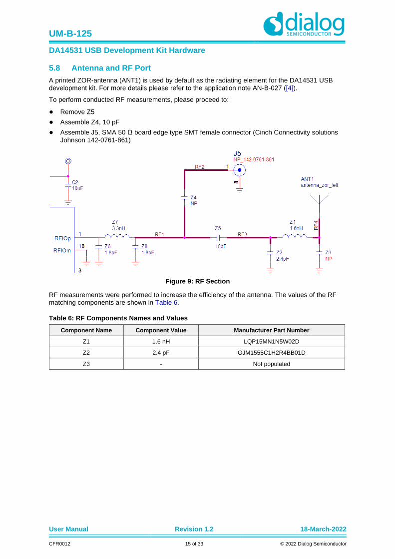
5.8 Antenna and RF Port
A printed ZOR-antenna (ANT1) is used by default as the radiating element for the DA14531 USB development kit. For more details please refer to the application note AN-B-027 ([4]).
To perform conducted RF measurements, please proceed to:
Remove Z5
Assemble Z4, 10 pF
Assemble J5, SMA 50 Ω board edge type SMT female connector (Cinch Connectivity solutions Johnson 142-0761-861)
Figure 9: RF Section
RF measurements were performed to increase the efficiency of the antenna. The values of the RF matching components are shown in Table 6.
Table 6: RF Components Names and Values
Component Name Component Value Manufacturer Part Number
Z1 1.6 nH LQP15MN1N5W02D
Z2 2.4 pF GJM1555C1H2R4BB01D
Z3 - Not populated
UM-B-125
DA14531 USB Development Kit Hardware
User Manual Revision 1.2 18-March-2022
CFR0012 16 of 33 © 2022 Dialog Semiconductor
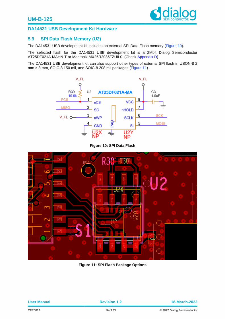
5.9 SPI Data Flash Memory (U2)
The DA14531 USB development kit includes an external SPI Data Flash memory (Figure 10).
The selected flash for the DA14531 USB development kit is a 2Mbit Dialog Semiconductor AT25DF021A-MAHN-T or Macronix MX25R2035FZUIL0. (Check Appendix D)
The DA14531 USB development kit can also support other types of external SPI flash in USON-8 2 mm × 3 mm, SOIC-8 150 mil, and SOIC-8 208 mil packages (Figure 11).
Figure 10: SPI Data Flash
Figure 11: SPI Flash Package Options
UM-B-125
DA14531 USB Development Kit Hardware
User Manual Revision 1.2 18-March-2022
CFR0012 17 of 33 © 2022 Dialog Semiconductor
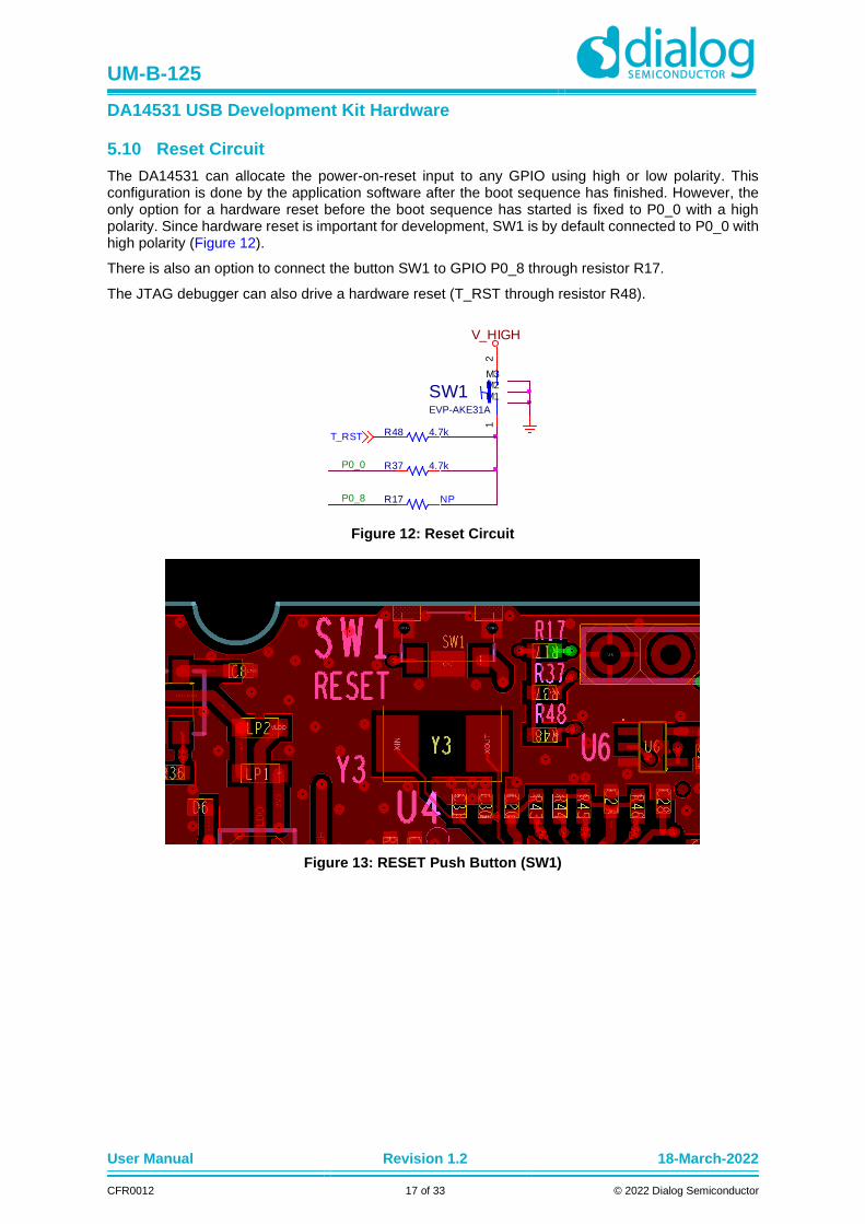
5.10 Reset Circuit
The DA14531 can allocate the power-on-reset input to any GPIO using high or low polarity. This configuration is done by the application software after the boot sequence has finished. However, the only option for a hardware reset before the boot sequence has started is fixed to P0_0 with a high polarity. Since hardware reset is important for development, SW1 is by default connected to P0_0 with high polarity (Figure 12).
There is also an option to connect the button SW1 to GPIO P0_8 through resistor R17.
The JTAG debugger can also drive a hardware reset (T_RST through resistor R48).
Figure 12: Reset Circuit
Figure 13: RESET Push Button (SW1)
R17 NPP0_8
P0_0
V_HIGH
R37 4.7k
T_RST R48 4.7k
SW1EVP-AKE31A
12
M1M2M3
UM-B-125
DA14531 USB Development Kit Hardware
User Manual Revision 1.2 18-March-2022
CFR0012 18 of 33 © 2022 Dialog Semiconductor
5.11 General Purpose Push Button
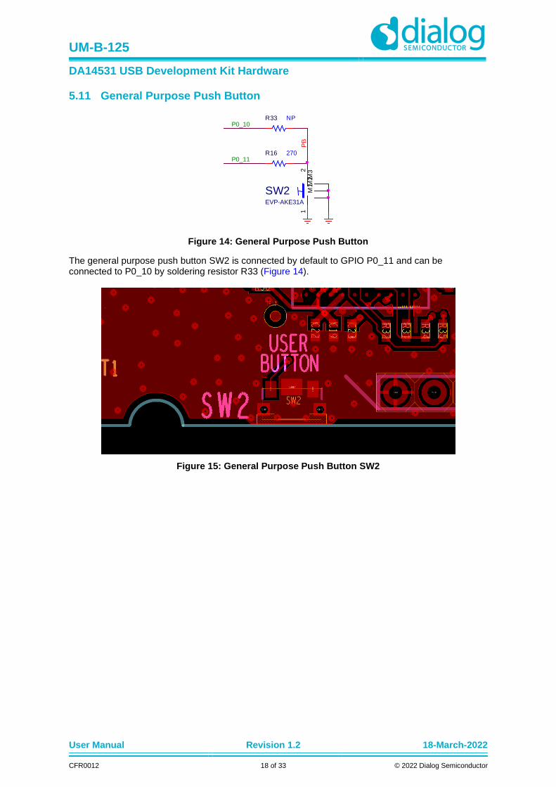
Figure 14: General Purpose Push Button
The general purpose push button SW2 is connected by default to GPIO P0_11 and can be connected to P0_10 by soldering resistor R33 (Figure 14).
Figure 15: General Purpose Push Button SW2
P0_11R16 270
SW2EVP-AKE31A
12
M1M
2M3
R33 NP
PB
P0_10
UM-B-125
DA14531 USB Development Kit Hardware
User Manual Revision 1.2 18-March-2022
CFR0012 19 of 33 © 2022 Dialog Semiconductor
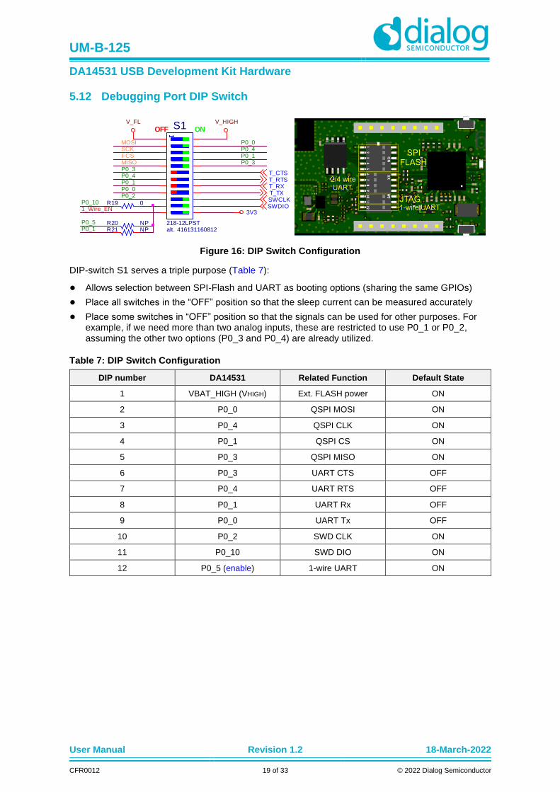
5.12 Debugging Port DIP Switch
Figure 16: DIP Switch Configuration
DIP-switch S1 serves a triple purpose (Table 7):
Allows selection between SPI-Flash and UART as booting options (sharing the same GPIOs)
Place all switches in the “OFF” position so that the sleep current can be measured accurately
Place some switches in “OFF” position so that the signals can be used for other purposes. For example, if we need more than two analog inputs, these are restricted to use P0_1 or P0_2, assuming the other two options (P0_3 and P0_4) are already utilized.
Table 7: DIP Switch Configuration
DIP number DA14531 Related Function Default State
1 VBAT_HIGH (VHIGH) Ext. FLASH power ON
2 P0_0 QSPI MOSI ON
3 P0_4 QSPI CLK ON
4 P0_1 QSPI CS ON
5 P0_3 QSPI MISO ON
6 P0_3 UART CTS OFF
7 P0_4 UART RTS OFF
8 P0_1 UART Rx OFF
9 P0_0 UART Tx OFF
10 P0_2 SWD CLK ON
11 P0_10 SWD DIO ON
12 P0_5 (enable) 1-wire UART ON
P0_10 R19 0
R20 NPP0_5P0_1 R21 NP
3V31_Wire_EN
T_TXT_RX
T_CTST_RTS
P0_3P0_4
P0_0P0_1
FCS P0_1MISO P0_3
P0_4SCK
P0_2
SWDIOSWCLK
S1
218-12LPST
OFF ONV_HIGHV_FL
alt. 416131160812
P0_0MOSI
UM-B-125
DA14531 USB Development Kit Hardware
User Manual Revision 1.2 18-March-2022
CFR0012 20 of 33 © 2022 Dialog Semiconductor
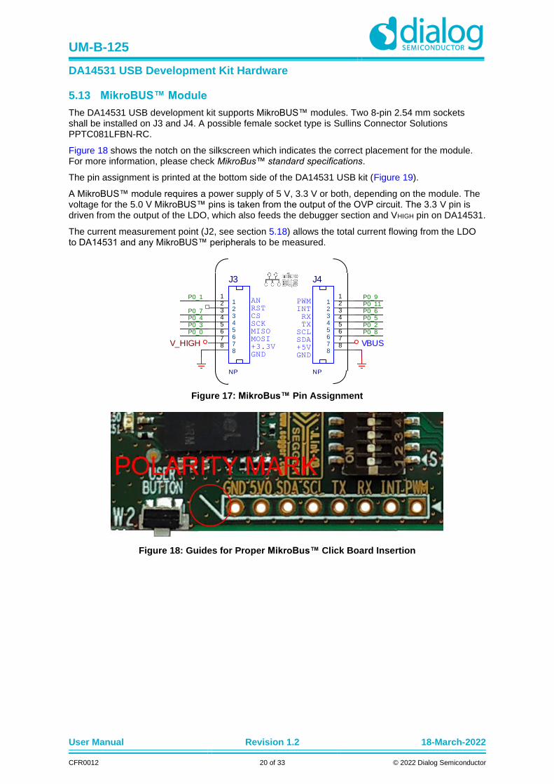
5.13 MikroBUS™ Module
The DA14531 USB development kit supports MikroBUS™ modules. Two 8-pin 2.54 mm sockets shall be installed on J3 and J4. A possible female socket type is Sullins Connector Solutions PPTC081LFBN-RC.
Figure 18 shows the notch on the silkscreen which indicates the correct placement for the module. For more information, please check MikroBus™ standard specifications.
The pin assignment is printed at the bottom side of the DA14531 USB kit (Figure 19).
A MikroBUS™ module requires a power supply of 5 V, 3.3 V or both, depending on the module. The voltage for the 5.0 V MikroBUS™ pins is taken from the output of the OVP circuit. The 3.3 V pin is driven from the output of the LDO, which also feeds the debugger section and VHIGH pin on DA14531.
The current measurement point (J2, see section 5.18) allows the total current flowing from the LDO to DA14531 and any MikroBUS™ peripherals to be measured.
Figure 17: MikroBus™ Pin Assignment
Figure 18: Guides for Proper MikroBus™ Click Board Insertion
PWMINTRXTX
SCLSDA+5VGND
ANRSTCSSCKMISOMOSI+3.3VGND
J3
NP
11
22
33
44
55
66
77
88
J4
NP
11
22
33
44
55
66
77
88 VBUSV_HIGH
P0_11P0_9
P0_5P0_6
P0_2P0_8P0_0
P0_3P0_4
P0_1
P0_7
UM-B-125
DA14531 USB Development Kit Hardware
User Manual Revision 1.2 18-March-2022
CFR0012 21 of 33 © 2022 Dialog Semiconductor
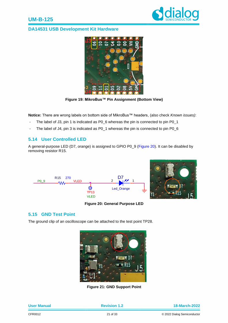
Figure 19: MikroBus™ Pin Assignment (Bottom View)
Notice: There are wrong labels on bottom side of MikroBus™ headers, (also check Known issues):
- The label of J3, pin 1 is indicated as P0_6 whereas the pin is connected to pin P0_1
- The label of J4, pin 3 is indicated as P0_1 whereas the pin is connected to pin P0_6
5.14 User Controlled LED
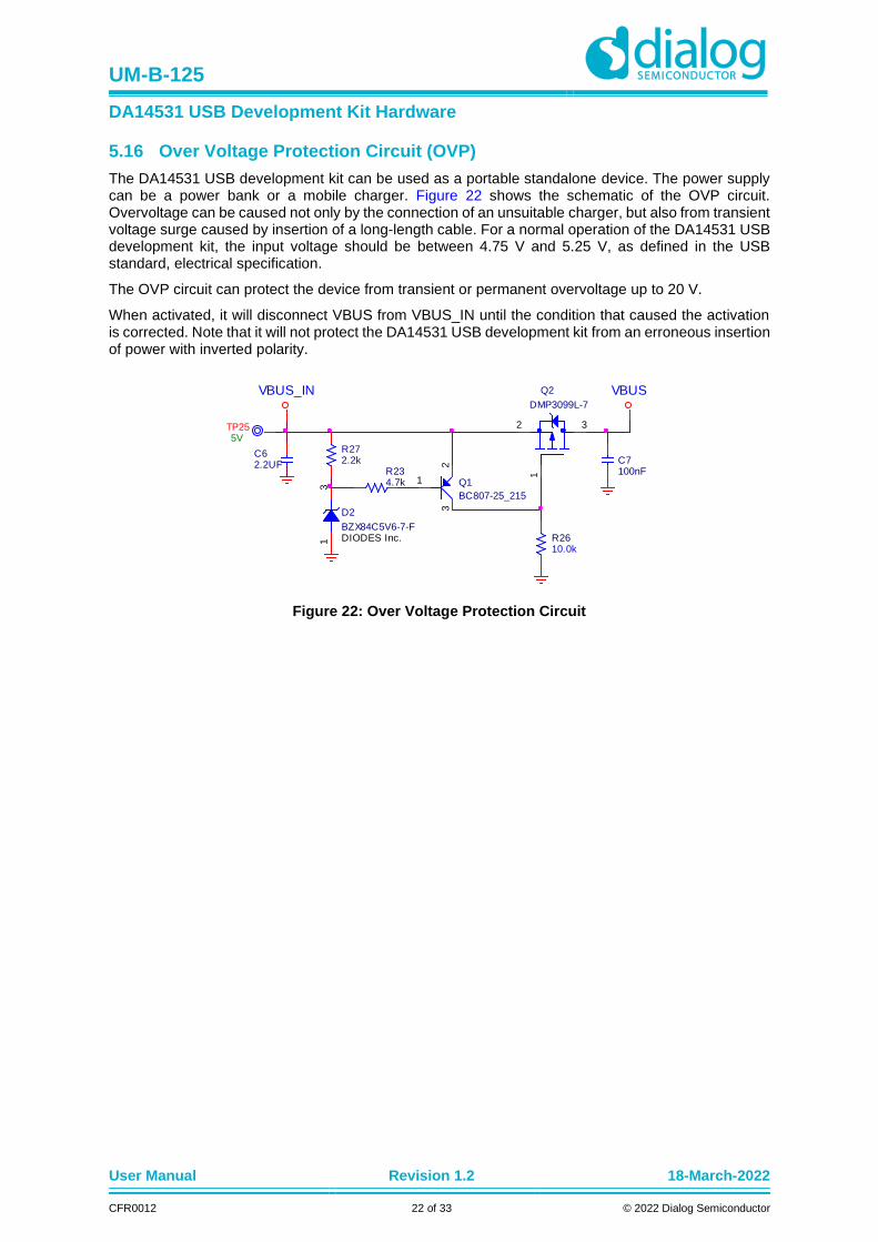
A general-purpose LED (D7, orange) is assigned to GPIO P0_9 (Figure 20). It can be disabled by removing resistor R15.
Figure 20: General Purpose LED
5.15 GND Test Point
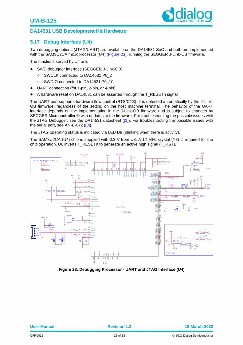
The ground clip of an oscilloscope can be attached to the test point TP28.
Figure 21: GND Support Point
VLEDD7
Led_Orange
2 1R15 270
TP13
VLED
P0_9
UM-B-125
DA14531 USB Development Kit Hardware
User Manual Revision 1.2 18-March-2022
CFR0012 22 of 33 © 2022 Dialog Semiconductor
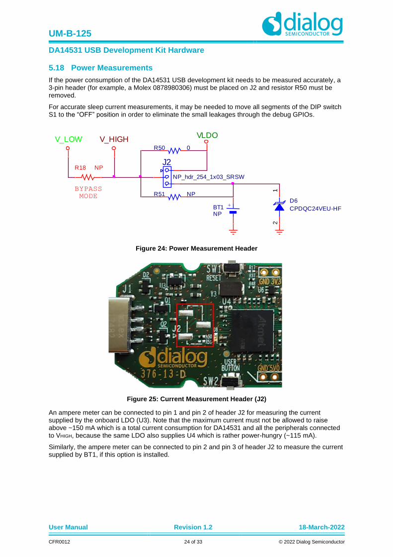
5.16 Over Voltage Protection Circuit (OVP)
The DA14531 USB development kit can be used as a portable standalone device. The power supply can be a power bank or a mobile charger. Figure 22 shows the schematic of the OVP circuit. Overvoltage can be caused not only by the connection of an unsuitable charger, but also from transient voltage surge caused by insertion of a long-length cable. For a normal operation of the DA14531 USB development kit, the input voltage should be between 4.75 V and 5.25 V, as defined in the USB standard, electrical specification.
The OVP circuit can protect the device from transient or permanent overvoltage up to 20 V.
When activated, it will disconnect VBUS from VBUS_IN until the condition that caused the activation is corrected. Note that it will not protect the DA14531 USB development kit from an erroneous insertion of power with inverted polarity.
Figure 22: Over Voltage Protection Circuit
TP255V
C7100nF
VBUS_IN
C62.2UF
R234.7k
DIODES Inc.
Q2
DMP3099L-7
3
1
2
D2
BZX84C5V6-7-F
13
R272.2k
R2610.0k
Q1
BC807-25_215
3
1
2
VBUS
UM-B-125
DA14531 USB Development Kit Hardware
User Manual Revision 1.2 18-March-2022
CFR0012 23 of 33 © 2022 Dialog Semiconductor
5.17 Debug Interface (U4)
Two debugging options (JTAG/UART) are available on the DA14531 SoC and both are implemented with the SAM3U2CA microprocessor (U4) (Figure 23), running the SEGGER J-Link-OB firmware.
The functions served by U4 are:
SWD debugger interface (SEGGER J-Link-OB)
SWCLK connected to DA14531 P0_2
SWDIO connected to DA14531 P0_10
UART connection (for 1-pin, 2-pin, or 4-pin)
A hardware reset on DA14531 can be asserted through the T_RESETn signal
The UART port supports hardware flow control (RTS/CTS). It is detected automatically by the J-Link-OB firmware, regardless of the setting on the host machine terminal. The behavior of the UART interface depends on the implementation in the J-Link-OB firmware and is subject to changes by SEGGER Microcontroller © with updates to the firmware. For troubleshooting the possible issues with the JTAG Debugger, see the DA14531 datasheet ([1]). For troubleshooting the possible issues with the serial port, see AN-B-072 ([3]).
The JTAG operating status is indicated via LED D8 (blinking when there is activity).
The SAM3U2CA (U4) chip is supplied with 3.3 V from U3. A 12 MHz crystal (Y3) is required for the chip operation. U6 inverts T_RESETn to generate an active high signal (T_RST).
Figure 23: Debugging Processor - UART and JTAG Interface (U4)
T_RTS
T_TXT_RX
T_CTS
C2810uF
XOUT
PA15
PA18
PA22
DFSDM
DFSDP
S_RXDS_TXD
PA29
TDIout
TDIin
VBG
PA4
NRSTB
TRSToutTRSTin
PA17
TRSToutTRSTin
TDIoutTDIin
Needed by Segger software
TDI
FWUP
ERASE
XIN
R35 330
C26100nF
C32 10nF
R40 36
R25 330
R4410.0k
R4310.0k
R42 0
TFBGA-100
ATSAM3U2CA-CU
U4
XINA2
XOUTA3
XIN32A10
NRSTB7
XOUT32B10
TMS/SWDIOC7
NRSTBC8
JTAGSELC9
TSTD7
FWUPD8
TCK/SWCLKA7
TDO/TRACESWOB8
TDIB9
ERASED6
VBGA1
DFSDPC1
DHSDPC2
VD
DB
UC
10
DFSDMD1
DHSDMD2
VD
DP
LL
D3
VD
DC
OR
E1
D4
VD
DIO
3E
6
VD
DC
OR
E2
E7
VD
DIO
1F
3
VD
DIO
2F
5
VD
DC
OR
E4
F9
VD
DC
OR
E5
G5
VD
DC
OR
E6
H1
AD
VR
EF
J3
VD
DA
NA
K2
AD
12B
VR
EF
K4
PB17A4
PB21A5
PB23A6
VD
DIN
A8
VD
DO
UT
A9
VD
DC
OR
E3
B1
GN
DU
TM
IB
2
VD
DU
TM
IB
3
PB10B4
PB18B5
PB24B6
GN
DP
LL
C3
PB14C4
PB19C5
PB22C6
PB20D5
PA11/PGMD3/URXDD9
PA12/PGMD4/UTXDD10
PA29E1
GN
D2
E2
PA28E3
PB9E4
GN
DB
UE
5
PA10/PGMD2E8PA9/PGMD1E9PA8/PGMD0E10
PB1F1
PB12F2
PA31F4
GN
D1
F6
PB16F7
PA6/PGMM2F8PA7/PGMM3F10
PB11G1
PB2G2
PB0G3
PB13G4
GN
D3
G6
PB15G7
PA3/PGMNVALIDG8
PA5/PGMM1G9PA4/PGMM0G10
PB5H2
PA27H3
PA22/PGMD14H4
PA13/PGMD5H5
PA15/PGMD7H6
PA18/PGMD10H7
PA24H8
PA1/PGMRDYH9
PA2/PGMNOEH10
PB6J1
PB8J2
PA30J4
PB3J5
PA16/PGMD8J6
PA19/PGMD11J7
PA21/PGMD13J8
PA26J9
PA0/PGMNCMDJ10
PB7K1
GN
DA
NA
K3
PB4K5
PA14/PGMD6K6
PA17/PGMD9K7
PA20/PGMD12K8
PA23/PGMD15K9
PA25K10
C2910pF
R28 330
R24 330
C20100nFC23
100nF
R34 330
R29 330
R46100.0k
C22100nF
C30 18pF
C24100nF
C31 18pF
C19100nF
R396.8k
R31 150
R22 150
C25100nF
R38
330
C21100nF
R4510.0k
R32 150
R41 36
VDD_COREVDD_CORE
Y3
12.0000MHZ
SWDIOSWCLK
J1
+5V1
D-2
D+3
GND4
VBUS_IN
USBDM
D1
CPDQC24VEU-HF
21
USBDP
S_nRTSS_nCTS
U6
NC7SZ04P5X
NC1
I2
GND3
O4
VCC5
T_RESETn
T_RST
C10 100nF
TP43V3
3V3
TP3VLDO
C8
NP
TP6
DBLED
C41.0uF
3V3
U3
NCP114ASN330T1G
IN1
GND2
EN3
NC4
OUT5
LP1
500mA_470 OHM
LP2
500mA_470 OHM
VLDO
C5
1.0uF
VBUS
3.3V LDO
R36100.0k
TP18
LDO_EN
TP35
TRTS
TP33
TCTS
TP36
TTX
TP34
TRX
TP21
SWDIO
TP22
SWCLK
C2710uF
TP11ERASE
TP8TDI
TP9TCK_SWCLK
TCK/SWCLK
TP30
SWO/TDO
SWO/TDO
TP10
TMS_SWDIO
TMS/SWDIO
TP12
NRST
3V3
3V3
3V3
3V3
3V3
D8
Led_Green
21
TP5
VDD_CORE
D3
CP
DQ
C5V
0C
SP
-HF
21
D4
CP
DQ
C5V
0C
SP
-HF
21
TP7GND
UM-B-125
DA14531 USB Development Kit Hardware
User Manual Revision 1.2 18-March-2022
CFR0012 24 of 33 © 2022 Dialog Semiconductor
5.18 Power Measurements
If the power consumption of the DA14531 USB development kit needs to be measured accurately, a 3-pin header (for example, a Molex 0878980306) must be placed on J2 and resistor R50 must be removed.
For accurate sleep current measurements, it may be needed to move all segments of the DIP switch S1 to the “OFF” position in order to eliminate the small leakages through the debug GPIOs.
Figure 24: Power Measurement Header
Figure 25: Current Measurement Header (J2)
An ampere meter can be connected to pin 1 and pin 2 of header J2 for measuring the current supplied by the onboard LDO (U3). Note that the maximum current must not be allowed to raise above ~150 mA which is a total current consumption for DA14531 and all the peripherals connected to VHIGH, because the same LDO also supplies U4 which is rather power-hungry (~115 mA).
Similarly, the ampere meter can be connected to pin 2 and pin 3 of header J2 to measure the current supplied by BT1, if this option is installed.
R50 0
R51 NP
J2
NP_hdr_254_1x03_SRSW
BYPASS MODE
V_LOWVLDO
V_HIGH
R18 NP
D6
CPDQC24VEU-HF
21
+
BT1NP
UM-B-125
DA14531 USB Development Kit Hardware
User Manual Revision 1.2 18-March-2022
CFR0012 25 of 33 © 2022 Dialog Semiconductor
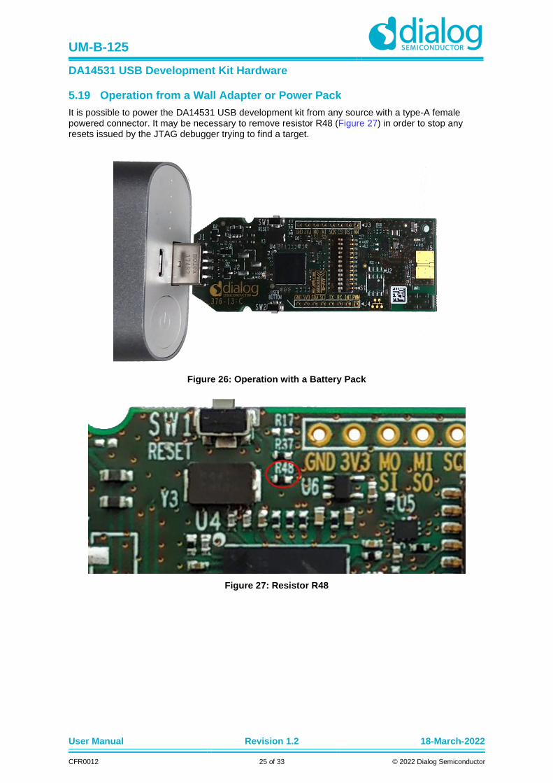
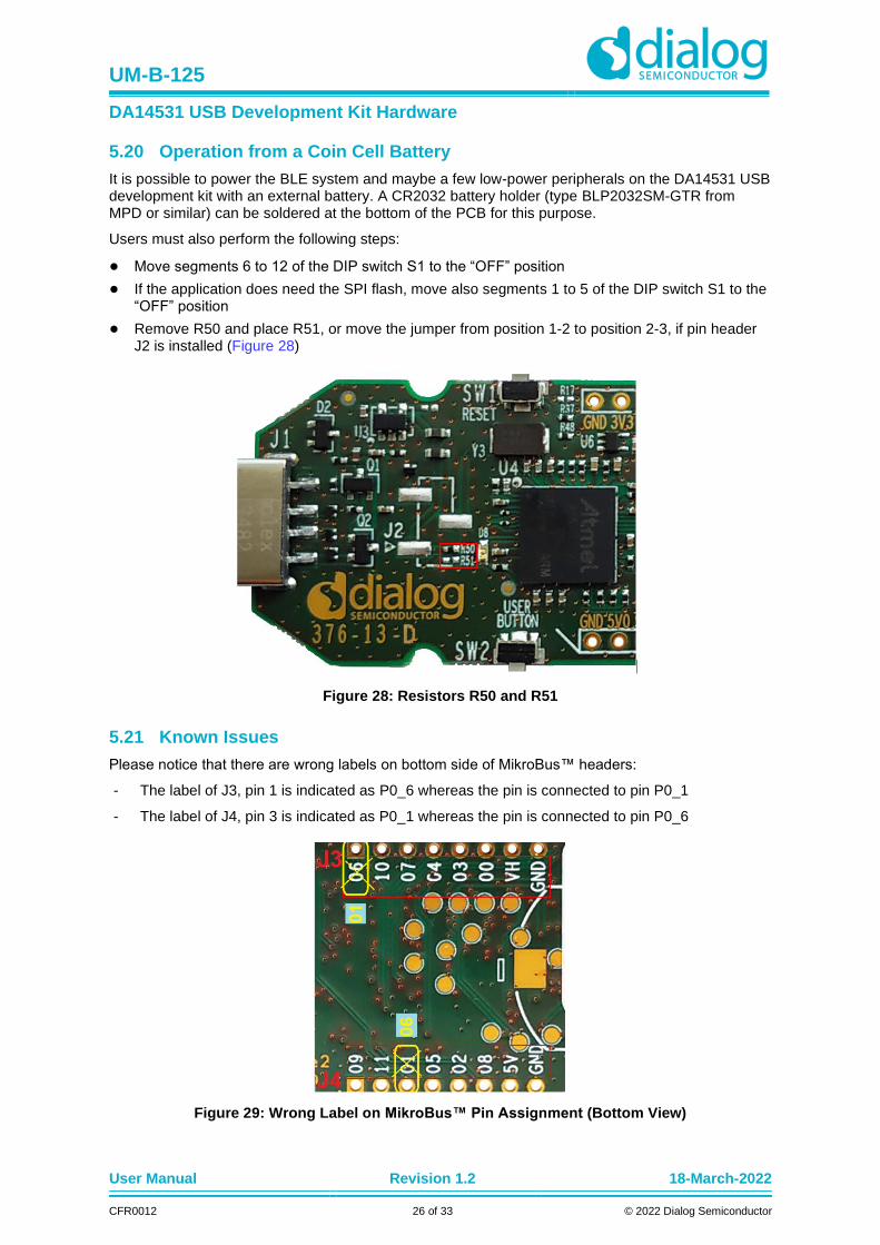
5.19 Operation from a Wall Adapter or Power Pack
It is possible to power the DA14531 USB development kit from any source with a type-A female powered connector. It may be necessary to remove resistor R48 (Figure 27) in order to stop any resets issued by the JTAG debugger trying to find a target.
Figure 26: Operation with a Battery Pack
Figure 27: Resistor R48
UM-B-125
DA14531 USB Development Kit Hardware
User Manual Revision 1.2 18-March-2022
CFR0012 26 of 33 © 2022 Dialog Semiconductor
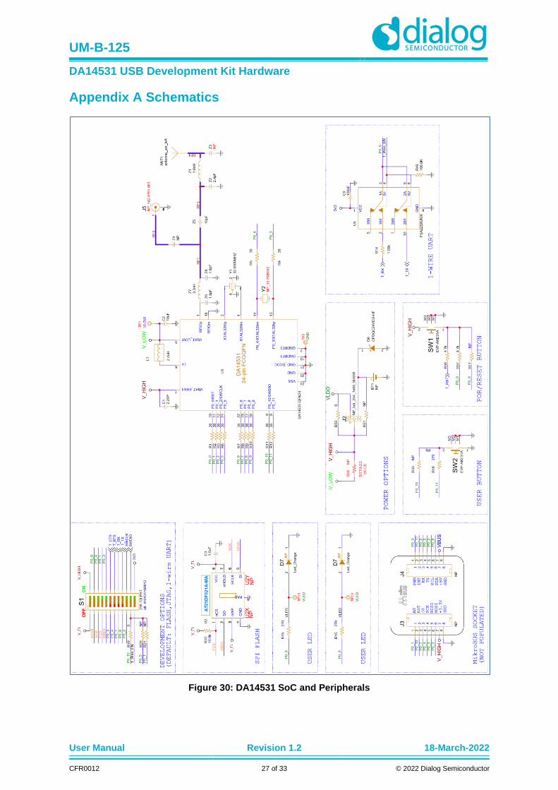
5.20 Operation from a Coin Cell Battery
It is possible to power the BLE system and maybe a few low-power peripherals on the DA14531 USB development kit with an external battery. A CR2032 battery holder (type BLP2032SM-GTR from MPD or similar) can be soldered at the bottom of the PCB for this purpose.
Users must also perform the following steps:
Move segments 6 to 12 of the DIP switch S1 to the “OFF” position
If the application does need the SPI flash, move also segments 1 to 5 of the DIP switch S1 to the “OFF” position
Remove R50 and place R51, or move the jumper from position 1-2 to position 2-3, if pin header J2 is installed (Figure 28)
Figure 28: Resistors R50 and R51
5.21 Known Issues
Please notice that there are wrong labels on bottom side of MikroBus™ headers:
- The label of J3, pin 1 is indicated as P0_6 whereas the pin is connected to pin P0_1
- The label of J4, pin 3 is indicated as P0_1 whereas the pin is connected to pin P0_6
Figure 29: Wrong Label on MikroBus™ Pin Assignment (Bottom View)
UM-B-125
DA14531 USB Development Kit Hardware
User Manual Revision 1.2 18-March-2022
CFR0012 27 of 33 © 2022 Dialog Semiconductor
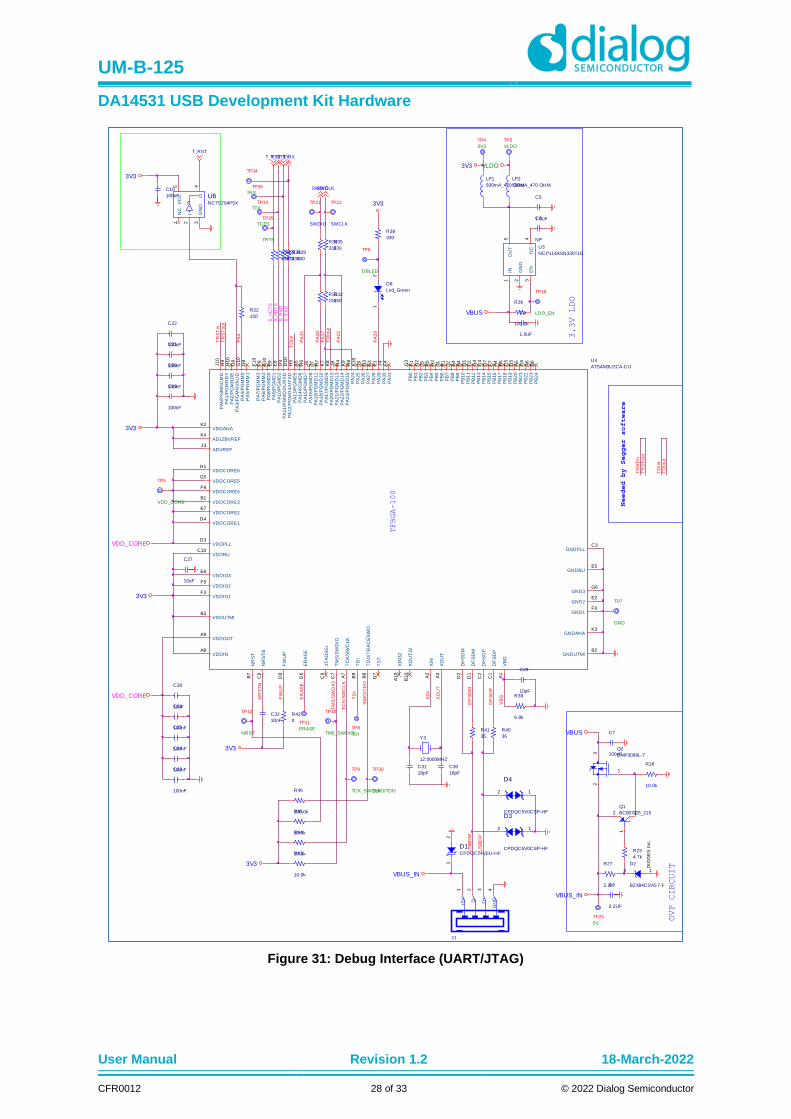
Appendix A Schematics
Figure 30: DA14531 SoC and Peripherals
UM-B-125
DA14531 USB Development Kit Hardware
User Manual Revision 1.2 18-March-2022
CFR0012 28 of 33 © 2022 Dialog Semiconductor
Figure 31: Debug Interface (UART/JTAG)
T_RTST_TXT_RXT_CTS
TP25
5V
C28
10uF
XO
UT
PA
22
PA
15
PA
18
DF
SD
P
DF
SD
M
S_T
XD
S_R
XD
TD
Iout
TD
Iin
PA
29
VB
GNR
ST
B
PA
4
TR
ST
in
TR
ST
out
TR
ST
in
PA
17
TD
Iout
TD
Iin
TR
ST
out
Needed by Segger software
FW
UP
TD
I
ER
AS
E
XIN
C26
100nF
R35
330
R40
36
C32
10nF
R25
330
R44
10.0k
R42
0
R43
10.0k
TFBGA-100
ATSAM3U2CA-CU
U4
XIN
A2
XO
UT
A3
XIN
32
A10
NR
ST
B7
XO
UT
32
B10
TM
S/S
WD
IOC
7
NR
ST
BC
8
JT
AG
SE
LC
9
TS
TD
7
FW
UP
D8
TC
K/S
WC
LK
A7
TD
O/T
RA
CE
SW
OB
8
TD
IB
9
ER
AS
ED
6
VB
GA
1
DF
SD
PC
1
DH
SD
PC
2
VDDBUC10
DF
SD
MD
1
DH
SD
MD
2
VDDPLLD3
VDDCORE1D4
VDDIO3E6
VDDCORE2E7
VDDIO1F3
VDDIO2F5
VDDCORE4F9
VDDCORE5G5
VDDCORE6H1
ADVREFJ3
VDDANAK2
AD12BVREFK4
PB
17
A4
PB
21
A5
PB
23
A6
VDDINA8
VDDOUTA9
VDDCORE3B1
GNDUTMIB2
VDDUTMIB3
PB
10
B4
PB
18
B5
PB
24
B6
GNDPLLC3
PB
14
C4
PB
19
C5
PB
22
C6
PB
20
D5
PA
11/P
GM
D3/U
RX
DD
9
PA
12/P
GM
D4/U
TX
DD
10
PA
29
E1
GND2E2
PA
28
E3
PB
9E
4
GNDBUE5
PA
10/P
GM
D2
E8
PA
9/P
GM
D1
E9
PA
8/P
GM
D0
E10
PB
1F
1
PB
12
F2
PA
31
F4
GND1F6
PB
16
F7
PA
6/P
GM
M2
F8
PA
7/P
GM
M3
F10
PB
11
G1
PB
2G
2
PB
0G
3
PB
13
G4
GND3G6
PB
15
G7
PA
3/P
GM
NV
ALID
G8
PA
5/P
GM
M1
G9
PA
4/P
GM
M0
G10
PB
5H
2
PA
27
H3
PA
22/P
GM
D14
H4
PA
13/P
GM
D5
H5
PA
15/P
GM
D7
H6
PA
18/P
GM
D10
H7
PA
24
H8
PA
1/P
GM
RD
YH
9
PA
2/P
GM
NO
EH
10
PB
6J1
PB
8J2
PA
30
J4
PB
3J5
PA
16/P
GM
D8
J6
PA
19/P
GM
D11
J7
PA
21/P
GM
D13
J8
PA
26
J9
PA
0/P
GM
NC
MD
J10
PB
7K
1
GNDANAK3
PB
4K
5
PA
14/P
GM
D6
K6
PA
17/P
GM
D9
K7
PA
20/P
GM
D12
K8
PA
23/P
GM
D15
K9
PA
25
K10
R24
330
C29
10pF
C20
100nF
R28
330
C23
100nF
R34
330
C22
100nF
R29
330
C30
18pF
R46
100.0k
C31
18pF
C24
100nF
C19
100nF
R39
6.8k
R22
150
R31
150
C25
100nF
R38
330
C21
100nF
R45
10.0k
VDD_CORE
R32
150
VDD_CORE
R41
36Y3
12.0000MHZ
SWDIOSWCLK
VBUS_IN
J1
+5V
1
D-
2
D+
3
GN
D4
D1CPDQC24VEU-HF
21
US
BD
P
US
BD
M
S_nC
TS
S_nR
TS
U6NC7SZ04P5X
NC
1
I2
GN
D3
O4
VC
C5
C10
100nF
T_RST
3V3
TP4
3V3
TP3
VLDO
C8
NP
C7
100nF
VBUS_IN
DIO
DE
S I
nc.
C6
2.2UF
Q2
DMP3099L-73
1
2
R23
4.7k
D2
BZX84C5V6-7-F
13
R27
2.2k
R26
10.0k
Q1
BC807-25_2153
1
2
OVP CIRCUIT
TP6
DBLED
C4
1.0uF
VBUS
3V3
U3
NCP114ASN330T1G
IN1
GN
D2
EN
3N
C4
OU
T5
LP1
500mA_470 OHM
VBUS
LP2
500mA_470 OHM
VLDO
3.3V LDO
C5
1.0uF
TP18
LDO_EN
R36
100.0k
TP36
TTX
TP35
TRTS
TP34
TRX
TP33
TCTS
TP22
SWCLK
TP21
SWDIO
TP11
ERASE
C27
10uF
TC
K/S
WC
LK
TP8
TDI
TP30
SWO/TDO
SW
O/T
DO
TP9
TCK_SWCLK
TP10
TMS_SWDIO
TM
S/S
WD
IO
3V3
3V3
3V3
TP12
NRST
3V3
3V3
D8
Led_Green
21
TP5
VDD_CORE
D4
CPDQC5V0CSP-HF
2 1
D3
CPDQC5V0CSP-HF
2 1
TP7
GND
UM-B-125
DA14531 USB Development Kit Hardware
User Manual Revision 1.2 18-March-2022
CFR0012 29 of 33 © 2022 Dialog Semiconductor
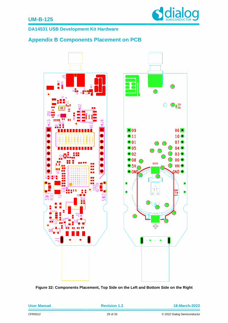
Appendix B Components Placement on PCB
Figure 32: Components Placement, Top Side on the Left and Bottom Side on the Right
UM-B-125
DA14531 USB Development Kit Hardware
User Manual Revision 1.2 18-March-2022
CFR0012 30 of 33 © 2022 Dialog Semiconductor
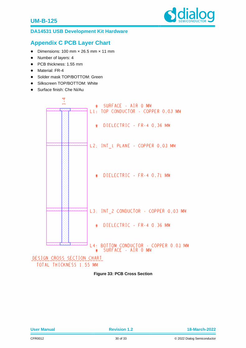
Appendix C PCB Layer Chart
Dimensions: 100 mm × 26.5 mm × 11 mm
Number of layers: 4
PCB thickness: 1.55 mm
Material: FR-4
Solder mask TOP/BOTTOM: Green
Silkscreen TOP/BOTTOM: White
Surface finish: Che Ni/Au
Figure 33: PCB Cross Section
UM-B-125
DA14531 USB Development Kit Hardware
User Manual Revision 1.2 18-March-2022
CFR0012 31 of 33 © 2022 Dialog Semiconductor
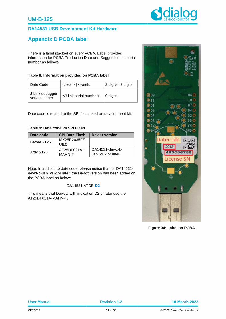
Appendix D PCBA label
There is a label stacked on every PCBA. Label provides information for PCBA Production Date and Segger license serial number as follows:
Table 8: Information provided on PCBA label
Date Code <Year> | <week> 2 digits | 2 digits
J-Link debugger serial number
<J-link serial number> 9 digits
Date code is related to the SPI flash used on development kit.
Table 9: Date code vs SPI Flash
Note: In addition to date code, please notice that for DA14531-
devkt-b-usb_vD2 or later, the Devkit version has been added on
the PCBA label as below:
DA14531 ATDB-D2
This means that Devkits with indication D2 or later use the
AT25DF021A-MAHN-T.
Date code SPI Data Flash Devkit version
Before 2126 MX25R2035FZ
UIL0
After 2126 AT25DF021A-
MAHN-T
DA14531-devkt-b-
usb_vD2 or later
Figure 34: Label on PCBA
UM-B-125
DA14531 USB Development Kit Hardware
User Manual Revision 1.2 18-March-2022
CFR0012 32 of 33 © 2022 Dialog Semiconductor
Revision History
Revision Date Description
1.2 18-March-2022 Added Known Issues section. Updated Flash and board revision.
Added Appendix D
1.1 09-Mar-2020 Updated Figure 8
1.0 22-Nov-2019 Initial version.
UM-B-125
DA14531 USB Development Kit Hardware
User Manual Revision 1.2 18-March-2022
CFR0012 33 of 33 © 2022 Dialog Semiconductor
Status Definitions
Status Definition
DRAFT The content of this document is under review and subject to formal approval, which may result in modifications or
additions.
APPROVED
or unmarked The content of this document has been approved for publication.
Disclaimer
Unless otherwise agreed in writing, the Dialog Semiconductor products (and any associated software) referred to in this document are not designed, authorized or warranted to be suitable for use in life support, life-critical or safety-critical systems or equipment, nor in applications where failure or malfunction of a Dialog Semiconductor product (or associated software) can reasonably be expected to result in personal injury, death or severe property or environmental damage. Dialog Semiconductor and its suppliers accept no liability for inclusion and/or use of Dialog Semiconductor products (and any associated software) in such equipment or applications and therefore such inclusion and/or use is at the customer’s own risk.
Information in this document is believed to be accurate and reliable. However, Dialog Semiconductor does not give any representations or warranties, express or implied, as to the accuracy or completeness of such information. Dialog Semiconductor furthermore takes no responsibility whatsoever for the content in this document if provided by any information source outside of Dialog Semiconductor.
Dialog Semiconductor reserves the right to change without notice the information published in this document, including, without limitation, the specification and the design of the related semiconductor products, software and applications. Notwithstanding the foregoing, for any automotive grade version of the device, Dialog Semiconductor reserves the right to change the information published in this document, including, without limitation, the specification and the design of the related semiconductor products, software and applications, in accordance with its standard automotive change notification process.
Applications, software, and semiconductor products described in this document are for illustrative purposes only. Dialog Semiconductor makes no representation or warranty that such applications, software and semiconductor products will be suitable for the specified use without further testing or modification. Unless otherwise agreed in writing, such testing or modification is the sole responsibility of the customer and Dialog Semiconductor excludes all liability in this respect.
Nothing in this document may be construed as a license for customer to use the Dialog Semiconductor products, software and applications referred to in this document. Such license must be separately sought by customer with Dialog Semiconductor.
All use of Dialog Semiconductor products, software and applications referred to in this document is subject to Dialog Semiconductor’s Standard Terms and Conditions of Sale, available on the company website (www.dialog-semiconductor.com) unless otherwise stated.
Dialog, Dialog Semiconductor and the Dialog logo are trademarks of Dialog Semiconductor Plc or its subsidiaries. All other product or service names and marks are the property of their respective owners.
© 2022 Dialog Semiconductor. All rights reserved.
RoHS Compliance
Dialog Semiconductor’s suppliers certify that its products are in compliance with the requirements of Directive 2011/65/EU of the European Parliament on the restriction of the use of certain hazardous substances in electrical and electronic equipment. RoHS certificates from our suppliers are available on request.
Contacting Dialog Semiconductor
United Kingdom (Headquarters)
Dialog Semiconductor (UK) LTD
Phone: +44 1793 757700
Germany
Dialog Semiconductor GmbH
Phone: +49 7021 805-0
The Netherlands
Dialog Semiconductor B.V.
Phone: +31 73 640 8822
North America
Dialog Semiconductor Inc.
Phone: +1 408 845 8500
Japan
Dialog Semiconductor K. K.
Phone: +81 3 5769 5100
Taiwan
Dialog Semiconductor Taiwan
Phone: +886 281 786 222
Hong Kong
Dialog Semiconductor Hong Kong
Phone: +852 2607 4271
Korea
Dialog Semiconductor Korea
Phone: +82 2 3469 8200
China (Shenzhen)
Dialog Semiconductor China
Phone: +86 755 2981 3669
China (Shanghai)
Dialog Semiconductor China
Phone: +86 21 5424 9058
Email:
Web site:
www.dialog-semiconductor.com


