Embed Size (px)
Citation preview

THÈSE Pour obtenir le grade de
DOCTEUR DE L’UNIVERSITÉ DE GRENOBLE Spécialité: OPTIQUE ET RADIOFREQUENCES
Arrêté ministériel: 7 août 2006 Présentée par
Bruno Roberto FRANCISCATTO Thèse dirigée par Tan Phu VUONG et codirigée par Jean-Marc DUCHAMP préparée au sein du l'Institut de Microélectronique Electromagnétisme et Photonique et le LAboratoire d'Hyperfréquences et de Caractérisation (IMEP-LAHC) dans l'École Doctorale Electronique, Electrotechnique, Automatique, Traitement du Signal (EEATS)
Conception et réalisation d’un nouveau transpondeur DSRC à faible consommation Thèse soutenue publiquement le 9 juillet 2014, devant le jury composé de :
Pr. Dr. Ke WU Ecole Polytechnique de Montréal, Président Pr. Dr. Laurent CIRIO Université Paris-Est Marne la Vallée, Rapporteur Pr. Dr. Mohammed HIMDI Université de Rennes I, Rapporteur Pr. Dr. Christian VOLLAIRE École Centrale de Lyon, Membre Mr. Christian DEFAY PDG Multitoll Solutions SA, Membre Pr. Dr. Tan Phu VUONG Université de Grenoble, Directeur de thèse Dr. Jean-Marc DUCHAMP Maître de Conférences à l’Université Joseph Fourier, Co-directeur de thèse


i
To
my fiancée Diana,
my parents and sister…

ii

iii
Remerciements
J’exprime ma gratitude et mes remerciements à mon directeur de thèse, Tan Phu
Vuong pour sa confiance et son soutien, tout en me laissant une large autonomie et à mon
co-encadrant Jean-Marc Duchamp, pour son énergie, ses conseils avisés et pertinents et
son professionnalisme qui m’ont été d’une aide précieuse et indispensable, et m’ont motivé à entreprendre cette aventure doctorale. Je tiens aussi à remercier mon co-
encadrant Mr. Christian Defay, PDG de la société Multitoll, qui m’a permis de réaliser ma thèse tout en gardant un poste d’ingénieur R&D chez Multitoll.
Cette thèse a été réalisée au laboratoire IMEP-LAHC à Grenoble, où j’ai passé de très
bons moments. Je tiens à remercier à tous les permanents du laboratoire qui ont su rendre
agréables ces années de thèse, à travers d’échanges techniques, mais aussi de moments
très joyeux en dehors du travail. Un grand merci à toute l’équipe technique responsable des plateformes de fabrication et caractérisation, Nicolas Corrao, Antoine Gachon et
Gregory Grosa, pas seulement pour leur efficacité au bon fonctionnement des
plateformes, mais surtout pour leur précises interventions techniques pendant les
différentes réalisations expérimentales de cette thèse. Je remercie également aux
différents post-doctorants, doctorants, ingénieurs de recherche et stagiaires que j’ai eu le plaisir de connaitre et avec lesquels j’ai pu collaborer pendant ces années dans le
laboratoire.
Je tiens également à remercier l’entreprise Multitoll, pour l’opportunité de pouvoir développer ma thèse en ayant un poste d’ingénieur. Ces années d’échanges professionnelles m’ont permis d’acquérir différentes compétences que j’emporterai avec
moi. Je remercie le bureau d’études, l’équipe d’installation et tests des systèmes et les ressources humaines pour tout le support. Je tiens à remercier spécialement à Mr. Tan
Trinh Trang qui a eu une participation importante dans cette thèse, aussi bien que dans
mon parcours professionnel.
Un grand merci tout particulier à ma fiancée Diana Stefan pour tout son support, sa
patience et sa compréhension pédant ces années de thèse. J’adresse mes pensées les plus chaleureuses à tous mes amis, qui m’ont supporté avec la thèse, mais aussi qui m’ont permis de vivre de bons moments inoubliables de détente, un grand merci à Vincent,
Vitor, Aline, Flora, Bertrand, Mauricio, …
Enfin, merci du fond du cœur à ma famille, mes parents, ma sœur et notre petite Maria Valentina, pour tout ce que je suis aujourd’hui grâce à vous! Obrigado, amo vocês!

iv
Abstract
To increase the efficiency and safety of the road traffic, new concepts and technologies
have been developed in Europe since 1992 for RTTT applications (Road Traffic & Transport
Telematics). These applications use the Dedicated Short Range Communications (DSRC)
devices at 5.8 GHz (ISM band). In view of the reliability and success of this technology, the
use of such equipment is thus extended to the EFC (Electronic Fee Collection) or e-toll and as
well in many other application areas such as fleet management, public transport and parking
management. Due to the broad applicability, these equipments are subject to various
standards CEN/TC 278, CEN ENV (EN) 12253, ETSI, etc.... The DSRC system consists in a
transceiver (reader) and transponders (tags). Industrial approaches are oriented to semi-
passive transponder technology, which uses the same signal sent by the reader to retransmit,
performing a frequency shift and encoding data to be transmitted. This design avoids the use
of the local oscillators to generate the RF wave, as in active transponders, and saves electrical
energy of batteries. This allows the development of relatively low cost and small size
transponders. Despite advances of low-power integrated circuits technology, this concept still
requires a lithium battery to operate the transponder for a period of 4-6 years. However, with
the expansion of these facilities, it appears that over the years the amount of lithium to
destroy has become a crucial problem for the environment. Nowadays designing a completely
autonomous DSRC transponder is not feasible, since the amount of energy required is still
high (8 mA/3.6 V active mode). Nevertheless, reducing the transponder electrical power
consumption, as a solution to at least double the battery life, could be a good start point to
improve environment protection.
In this thesis we propose a new DSRC transponder with an original statechart that
considerably reduces the power consumption. After validation of the new low-power
consumption mode, we have investigated the possibility to recharge the battery of the
transponder by means of Wireless Energy Harvesting. The DSRC Toll Collection RF link
budget has been carried out in order to estimate the amount of energy available when a car
with a transponder passes through a toll system. However, RF link budget at 5.8 GHz
presents a low power density, since the car does not remain enough in the DSRC antenna’s field to proceed to energy harvesting. Therefore, we have explored another ISM frequency,
the 2.45 GHz. Thus the Wireless Energy Harvesting chapter aims to further the state of the art
by the design and optimization of a novel RF harvesting board. We have demonstrated that an
optimum RF-DC load is required in order to achieve high RF-DC conversion efficiency.
Several rectifiers and rectennas have been prototyped in order to validate the numerical
studies. Finally, the results obtained in this thesis are in the forefront of the State-of-the-Art
of Wireless Energy Harvesting for very low available power density.
Keywords: DSRC, Wireless Energy Harvesting, antenna, rectenna, transponder, RF-DC
conversion

v
Résumé
Afin d’augmenter l’efficacité et la sécurité du trafic routier, de nouveaux concepts et
technologies ont été développés depuis 1992 en Europe pour les applications RTTT (Road
Traffic & Transport Telematics). Ces applications utilisent les équipements DSRC qui
supportent les transmissions à courte distance à 5.8GHz. Vues la fiabilité et le succès de cette
technologie, l’utilisation de ces équipements est ensuite étendue aux ETC (Electronic Toll Collection) ou Télépéage et aussi dans une multitude d’autres domaines d’application comme la gestion des flottes, le transport public et la gestion des parkings. Le système DSRC se
compose d’un émetteur/récepteur (lecteur) et des transpondeurs (badges). En toute logique,
l’approche industrielle oriente les développements vers la technologie de transpondeur semi passif qui, pour réémettre un signal utilise le signal transmis par l’émetteur–récepteur,
effectue une modulation de phase d’une sous porteuse fréquentielle encodant ainsi les
données à transmettre. Cette conception évite l’utilisation des oscillateurs locaux, comme dans les transpondeurs actifs, pour générer l’onde Radio Fréquence (RF). Ceci permet de produire des transpondeurs relativement à faible coût et de petite taille. Cependant ce concept
nécessite quand même une batterie au Lithium pour assurer le fonctionnement du
transpondeur pour une durée de 4 à 6 ans et ce malgré les progrès des technologies de circuits
intégrés à faible consommation. Au fur et à mesure de l’expansion de ces équipements, il s’avère qu’avec les années la quantité des batteries au lithium à détruire deviendrait un problème crucial pour l’environnement. Aujourd’hui, la conception d’un transpondeur DSRC complètement autonome n'est pas faisable, car la quantité d'énergie nécessaire s’avère encore élevée (mode actif 8 mA/3.6 V). Néanmoins, la réduction de la consommation électrique du
transpondeur, permet au moins doubler la durée de vie de la batterie et pourrait être un bon
point de départ pour améliorer la protection de l’environnement.
Dans cette thèse, nous proposons un nouveau transpondeur DSRC avec un diagramme
d'état original qui réduit considérablement la consommation énergétique. Après validation
d’un nouvel état de fonctionnement en mode très faible consommation d'énergie, nous avons
étudié la possibilité de recharger la batterie du transpondeur à travers de la récupération
d'énergie sans fil. Le bilan de liaison énergétique DSRC a été réalisé afin d'estimer la quantité
d'énergie disponible quand une voiture avec un transpondeur passe à sous un système de
péage. Toutefois, le bilan énergétique à 5.8 GHz présente une faible densité d’énergie RF, puisque la voiture ne reste pas assez sur le lobe de l'antenne DSRC afin de procéder à la
récupération d’énergie. Par conséquent, nous avons alors exploré une autre fréquence ISM, le 2.45 GHz dans laquelle la présence d’émetteurs est bien plus grande. Dans le chapitre de récupération d'énergie sans fil nous présentons la conception et l'optimisation d'un nouveau
récupérateur d’énergie RF. Après avoir démontré qu’une charge RF-DC optimale est
nécessaire afin d'atteindre une haute efficacité de conversion RF-DC. Plusieurs redresseurs et
rectennas ont été conçus pour valider les études numériques. Parmi, les résultats présentés
dans cette thèse les rendement de conversion obtenus sont à l'état de l’art de la récupération d'énergie sans fil pour une très faible densité de puissance disponible.
Mots clés: DSRC, récupération d'énergie sans fil, antenne, rectenna, transpondeur,
conversion RF-DC

vi
Contents
Chapter I - Introduction and State-of-the-Art .................................................................................. 1
I.1. Context ................................................................................................................................... 1
I.1.1. Transponder architecture ............................................................................................... 2
I.1.2. Process technology choice .............................................................................................. 4
I.1.3. RF protocol ...................................................................................................................... 5
I.1.4. Potential Energy Harvesting techniques ......................................................................... 7
I.1.4.1. Solar ..................................................................................................................... 9
I.1.4.2. Thermoelectric ................................................................................................... 10
I.1.4.3. Mechanical ......................................................................................................... 11
I.1.4.4. Radio frequency (RF) .......................................................................................... 12
I.1.4.4.1. Why Wireless Energy Harvesting? ................................................................. 15
I.1.4.4.2. State-of-the-Art of Wireless Energy Harvesting ............................................. 19
I.2. Problem statement: is it possible to design a completely autonomous DSRC transponder?
................................................................................................................................................... 22
I.3. Thesis overview .................................................................................................................... 23
Chapter II - Low-power DSRC transponder .................................................................................... 24
II.1. Introduction ........................................................................................................................ 24
II.2. DSRC system ........................................................................................................................ 24
II.2.1. Literature overview ...................................................................................................... 30
II.2.2. DSRC V2I link budget .................................................................................................... 31
II.2.2.1. Windshield fading .......................................................................................... 34
II.2.2.2. DSRC V2I link budget results .......................................................................... 35
II.3. A new low-power DSRC transponder design ...................................................................... 40
II.3.1. Electric power consumption of DSRC transponders on the current market ............... 40
II.3.1.1. Measurement setup ....................................................................................... 41
II.3.1.2. Electric power consumption measurements results ..................................... 42
II.3.1.3. The importance of a low-power operation mode ......................................... 44
II.3.2. RF implementation ....................................................................................................... 44
II.3.2.1. DSRC transponder chip evaluation board design .......................................... 44
II.3.2.2. DSRC transponder chip characterization ....................................................... 47
II.3.3. Microcontroller sleep mode + Demod Bloc (FPGA) ..................................................... 51
II.3.4. A new deep-sleep mode .............................................................................................. 51
II.3.4.1. Vibration sensor evaluation board design ..................................................... 53

vii
II.3.4.2. In-situ deep-sleep tests .................................................................................. 55
II.3.5. The energy consumption of the proposed DSRC transponder .................................... 56
II.4. Conclusions .......................................................................................................................... 57
Chapter III - Antenna design ........................................................................................................... 59
III.1. Introduction ........................................................................................................................ 59
III.2. Antenna fundamentals ....................................................................................................... 59
III.2.1. How an antenna radiates ............................................................................................ 59
III.2.2. Fundamental parameters of Antennas ....................................................................... 60
III.2.2.1. Radiation pattern (farfield) ............................................................................. 60
III.2.2.2. Beamwidth ..................................................................................................... 61
III.2.2.3. Return loss and reflection coefficient ............................................................ 61
III.2.2.4. Bandwidth ...................................................................................................... 62
III.2.2.5. Antenna efficiency .......................................................................................... 62
III.2.2.6. Gain ................................................................................................................. 62
III.2.2.7. Polarization ..................................................................................................... 63
III.2.3. Near and Far field regions ........................................................................................... 64
III.2.4. Different antenna types .............................................................................................. 66
III.3. Antenna design ................................................................................................................... 67
III.3.1. Multitoll antenna specifications .................................................................................. 67
III.3.2. Microstrip antenna ...................................................................................................... 67
III.3.3. DSRC antennas............................................................................................................. 69
III.3.3.1. DSRC OBU antenna ......................................................................................... 69
III.3.3.2. DSRC RSE antennas ......................................................................................... 72
III.3.3.2.1. Patch antenna array with superstrate............................................................ 72
III.3.3.2.2. Patch antenna array with an improved circular polarization ......................... 77
III.3.3.2.3. DSRC RSE antennas in-situ tests ..................................................................... 85
III.3.4. Wireless Energy Harvesting antennas ......................................................................... 90
III.3.4.1. Antenna design (Rectenna #1) ....................................................................... 90
III.3.4.2. Antenna design (Rectenna #2) ....................................................................... 92
III.4. Conclusion .......................................................................................................................... 93
Chapter IV - Wireless Energy Harvesting ........................................................................................ 95
IV.1. Introduction to Wireless Energy Harvesting ...................................................................... 95
IV.2. Zero-bias Schottky Diode modeling ................................................................................... 98
IV.3. Analysis of the optimum load impedance to improve the RF-DC conversion efficiency . 104

viii
IV.4. Microstrip line .................................................................................................................. 111
IV.5. WEH device design .......................................................................................................... 112
IV.5.1. Design of rectifiers .................................................................................................... 112
IV.5.1.1. Rectifier prototype #1 .................................................................................. 112
IV.5.1.2. Rectifier prototype #2 .................................................................................. 118
IV.5.1.3. Rectifier prototype #3 .................................................................................. 121
IV.5.1.4. Rectifier prototype #4 .................................................................................. 122
IV.5.1.5. Rectifier prototype #5 .................................................................................. 125
IV.5.2. Design of the rectennas ............................................................................................ 127
IV.5.2.1. Rectenna prototype #1 ................................................................................ 129
IV.5.2.2. Rectenna prototype #2 ................................................................................ 131
IV.6. Conclusion, comparison with the state of the art and perspectives for future work ..... 133
Chapter V - Conclusion and perspectives .................................................................................... 139
V.1. Summary of results ........................................................................................................... 139
V.2. Perspectives ...................................................................................................................... 142
References ................................................................................................................................... 144
Publications .................................................................................................................................. 154

ix
Acronyms
BST Beacon Service Table DSRC Dedicated Short Range Communication EH Energy Harvesting ETC Electronic Toll Collection ETSI European Telecommunications Standards Institute IC Integrated Circuit ISM Industrial Scientific Medical ITS Intelligent Transport Systems LNA Low Noise Amplifier LO Local Oscillator OBU On-Boar Unit PA Power Amplifier RF Radio Frequency RFID Radio-Frequency IDentification RSE Road Side Equipment RTTT Road Traffic & Transport Telematics V2I Vehicle-to-Infrastructure V2V Vehicle-to- Vehicle WEH Wireless Energy Harvesting WPT Wireless Power Transfer WS Wireless Sensor WSN Wireless Sensor Network


Chapter I - Introduction and State-of-the-Art 1
Chapter I - Introduction and
State-of-the-Art
I.1. Context
Engineers are often confronted to improve the system functionality and performances
objective while simultaneously maximizing the battery life of electronic devices. From
the consumer’s viewpoint, they are expecting more and more functionality in a smaller device that operates for a long time, whose battery does not need to be changed often. The
common point is the battery; the maintenance cost can be very high and in some cases the
replacement is really difficult (e.g.: sensors inside the walls of a house). To effectively
design electronic devices with a longer battery life, or even without battery, one should
consider the power optimization at all levels, from the circuit architecture up to the
application layer. Nowadays, Wireless Sensors (WS) are able to realize three activities,
with the associated energy cost, Fig. I-1.
Fig. I-1. Classical WS diagram illustrating the different power consumption for each operation mode.
However, the power consumption for each operation mode, should be observed taking
into account the period to accomplish the task, Fig. I-2.
Fig. I-2. WS power consumption for different operation mode.
Battery
µCFront end
Radio Sensors
*Guardians Angels European flagship project

2 Chapter I - Introduction and State-of-the-Art
One first possibility towards maximizing the battery life is by reducing the power
consumption. However, we are looking for power reduction not only at an instantaneous
time, but over the life of the product. In this case, we introduce the concept of energy,
which is the integral of power over a period of time. In general, we may define the total
energy consumed by an electronic device as:
(I-1)
For low-power battery-powered applications (e.g.: sensors), the standby mode is
predominant and thus its energy requirement impacts directly the battery life. Therefore,
before starting the device design, engineers may interrogate themselves on some
hypothetical points about the application:
What is the statechart of the device and how much time is necessary for each
operation mode?
Reduce functional blocks on the RF front-end, decrease the power
consumption. Which ones are really necessary?
When the microcontroller is not running, in a deep-sleep mode, how is its
wake-up induced?
Which is the microelectronic technology that allows the lowest power
consumption (or lowest bias current)?
The answer for these questions may help during the optimization process aiming for
energy reduction.
Nowadays, most of the low-powered applications need Radio Frequency (RF)
transponders for different reasons: a RF link is necessary to the exchange data between
Tx and Rx (e.g.: DSRC), the energy necessary to supply the device may be provided by
the RF signal (e.g.: RFID)…
In order to improve the battery life and functionality of the low-powered devices, some
approaches may be explored: the optimization of the transponder architecture, the energy
required by each electronic component should be efficiently shared and each operation
mode should be correctly explored; the process technology choice, since the
microcontroller is a primary power consumer, and the way that energy is used should be
carefully considered; the RF protocol can be modified (in some cases), saving energy;
and finally, new approaches in which is efficiently possible to recharge the battery by
means of energy harvesting have been reported.
I.1.1. Transponder architecture
With the purpose of exemplifying transponder architectures, let us consider the case of
a classical active transponder, where several electronic components are required to
provide a correct reception and transmission of signals, as described in Fig. I-3. In active

Chapter I - Introduction and State-of-the-Art 3
transponder architecture, the energy is mostly dissipated on the Low Noise Amplifier
(LNA), Power Amplifier (PA), Local Oscillator (LO) and microcontroller.
Fig. I-3. Typical active transponder architecture.
Depending on the application, some blocs of the active transponder may be eliminated,
e.g., the local oscillator, PA and LNA. Thus, by using a backscattering method, the
transponder can recover the incoming carrier to modulate the uplink data stream, and
consequently the power is considerably reduced. This architecture is named backscatter
transponder, an example of its circuit diagram being described in Fig. I-4.
Fig. I-4. Typical backscatter transponder architecture.
However, the backscatter transponder should be ready to reply the reader’s request at anytime, i.e., the transponder should be able to leave the standby mode very quickly. In
order to reduce the power consumption of a backscatter transponder, a simple approach
may be applied, a supplementary wake-up bloc may be added, creating a supplementary
very-low-power mode (deep-sleep). As a result, the transponder is active only when the
RF transaction is imminent. Evidently, the protocol and statechart should be modified in
order to predict the new operation mode.
Owing to advances in integrated low-power circuit technology, nowadays, completely
passive transponders are also available. In most of the cases, the energy required by the
transponder is provided by a RF wake-up signal (e.g.: RFID tags). Moreover, an
important progress has been done in order to reduce the power consumption of RF
transponders, thus a new approach is emerging, i.e., low-power devices may be powered
by means of Energy Harvesting.
Furthermore, depending on the application, the transponder architecture may be
considerably optimized by reducing the energy consumption. Implementing different
BPFLNA
LPF
PA BPF
Rx_IF
LO
Tx_IF
LPF
µC
BPF BPF
µC
Detector
Sub-carrier oscilator
Modulator
BPF
Rx
Tx
COM
BackScasignal

4 Chapter I - Introduction and State-of-the-Art
operation modes also helps saving energy in a more efficient manner. Nevertheless, to
implement a complex statechart, the microcontroller choice should be correctly done.
I.1.2. Process technology choice
The process technology has been improved continuously, and definitely it continues
reaching physical limitations. Furthermore, due to the increased demand of faster and
smaller, low-power chips, the geometry shrink is an important candidate to manage low-
power, Fig. I-5. Currently, 22/16nm chips are already available, and 11nm are very soon
coming.
The next graph contains a lot of information, if you take the time to parse it, you can
observe interesting points, e.g.: the size of the transistor proposed by Xeonis about half of
the size of a HIV virus.
Fig. I-5. Lithography scaling.
The semiconductor technology has been improved and leads to lower power
consumption, smaller dimensions of transistors, higher packaging density and faster
circuits. From a simple sensor to a complex system, they need at least a chip to take the
decisions. Despite the advances in semiconductor technology, the chip is still one of the
sources of power dissipation in an electronic device. However, this element does not need
to be active or running on the maximum clock frequency at all times. Nowadays, several
microcontrollers available on the market have at least three operation modes (deep-sleep,
stand-by and active) and, as well, the frequency of the clock can be gradually varied.
Reducing power consumption in active mode only saves energy if the time required to
accomplish the task does not increase too much. We aim at keeping the statechart in the
deep-sleep mode as long as possible.
*S
ourc
e : T
hom
as D
ean
– Goo
gle
Inc.

Chapter I - Introduction and State-of-the-Art 5
By understanding the potential in the use of the different operation modes, frequency
clock control and the many ways of microcontrollers energy consumption, the
functionality and battery life of low-power devices may be improved.
I.1.3. RF protocol
Communication applications range from simple RFID transponders to cell phones and
cognitive radios or even systems where security enforcement is necessary to guarantee
payment transactions (e.g.: DSRC electronic toll collection). Depending on the
application, several protocols are available and in some cases the RF protocol can be
modified in order to reduce the energy consumption. A good example of a RF protocol
evolution is the RFID, in which first the energy necessary to wake-up the tag is sent and
then the tag executes the instructions of reception and transmission.
In indoor applications, Wireless Sensor Network (WSN) appears to be a huge
opportunity for protocol development, as energy consumption is a key point for low-
power sensors. We could cite as classical RF protocols for indoor applications: WiFi,
Bluetooth and ZigBee. However, recently several companies emerged, providing specific
RF protocols optimized for very-low-power or completely autonomous sensors
integrating a WSN: enocean, WirelessHart, z-wave, dash7, MyriaNED… In Fig. I-6, we
have a comparison of different indoor RF protocols considering the energy required, as
well the indoor range. It should be noticed that if the energy requirements decrease, the
battery problem can be easily cancelled out, transforming the devices in battery-less
sensors.
Fig. I-6. Comparison of RF protocols optimized for Wireless Sensor Network.
In outdoor applications, as different RF protocols exist, let us consider as example a
particular application, the Electronic Toll Collection (ETC) or e-toll, which employs at
least two RF protocols: DSRC and RFID. ETC is based on collecting tolls electronically
at toll stations, preventing the traffic jam and providing a faster and safer trip for the
drivers.
*
So
urc
e :
en
oce
an
we
bsi
te

6 Chapter I - Introduction and State-of-the-Art
Over the years, for RFID, an important effort has been done in order to transform the
RFID tags into completely passive devices. Due to the battery elimination, the fabrication
cost was considerably reduced and nowadays for less than $2, RFID tags are sold all over
the world. However, in the case not only the ID is required, and writing information on
the tag is necessary, depending on the amount of data, using semi-passive tags is
unavoidable. In ETC applications, some countries use RFID as RF protocol for the road
fee collection. The advantage is the final cost of the system that is really cheap when
compared to DSRC protocols, as passive tags can be used and several are the RFID tags
and readers available on the market. On the other hand, the RFID protocol does not
provide enough complexity levels in order to guarantee a safe electronic payment and
consequently can be easily hacked.
DSRC protocol emerged in Europe and it is a complete system designed for vehicle-to-
vehicle (V2V) and vehicle-to-infrastructure (V2I) communications. In a V2I
communication, this protocol may be deployed for e-toll applications. The advantage of
DSRC protocol is the existence of several layers of complexity that guarantee a safe
payment transaction. Moreover, DSRC provides a higher data rate than RFID. Due to the
amount of data exchanged in a DSRC transaction, the transponder is semi-passive (has a
battery). However, industrial European approaches designed the DSRC transponder based
on the backscatter method, which uses the same signal sent by the reader to retransmit,
perform a frequency shift and encode data to be transmitted. Due to this improvement the
DSRC transponder does not need a local oscillator and the energy consumption is
considerably reduced. The DSRC protocol is detailed later on in this thesis.
Choosing the RF protocol, if it is possible, is a key point to guarantee the efficiency of
the application, by finding a compromise with power consumption. The combination of
authorized radiated power (E.R.I.P), data rate and radio sensitivity provides developers
with the flexibility to optimize their implementation for range, cost, operating life and
ease of installation. In Table I.1, some RF protocols are compared based on EU standards.
TABLE I.1. RF PROTOCOLS
RF protocol Radiated power (E.I.R.P.) Data rate+ Frequency Radio sensitivity§
WiFi° 100mW# 11-105Mbps 2.45GHz -80dBm
Bluetooth° 1mW# 1Mbps 2.45GHz -70dBm
ZigBee° 1mW# 250kbps 2.45GHz -85dBm
RFID 2W* 128kbps 868-915MHz -20dBm
DSRC 2W* 500kbps 5.8GHz -60dBm °Symmetric protocol,
#indoor,
*outdoor,
+downlink(Tx->Rx),
§Rx
From the RF link budget, the range can be determined by the sensitivity of the
transceiver and its maximum authorized radiated power. In Fig. I-7, several RF protocols
are presented by finding a compromise between the power consumption, complexity/cost
and data rate.

Chapter I - Introduction and State-of-the-Art 7
Fig. I-7. RF protocols showing compromise between the power consumption, complexity/cost and data rate.
I.1.4. Potential Energy Harvesting techniques
The effort over the years in reducing the energy consumption of the transponders, by
optimizing the architecture, process technology and RF protocol, is being repaid by an
emergent concept, that is, the low-power devices can be powered by means of ambient
Energy Harvesting (EH). The energy harvesting concept comes at a time when the
“compromise point” between energy consumed and harvested may be achieved.
Energy harvesting may be defined as the conversion process of ambient energy into
electrical energy. Radiant (solar, infrared, radiofrequency), thermal, mechanical and
biochemical are examples of the ambient energy that surrounds us and thus potential
candidates for energy harvesting sources, as described in Fig. I-8. Energy harvesting or
scavenging becomes an interesting environmental friendly solution regarding the devices
batteries. Even if long-life batteries will still be unavoidable, as technologies mature,
energy harvesting is creating some shift in battery usage from primary to rechargeable
batteries. However, the biggest potential of energy harvesting is creating a new class of
electronic devices that do not need battery, i.e., battery-less, as they are completely
powered by ambient sources. Thus, at same time the device cost is clearly reduced and an
alternative is provided for the battery discarding problem.
Fig. I-8. Energy harvesting sources.
Energy Harvesting
Mechanical sources
Stress-Strains
Vibration
Thermalsources
Thermalgradient/ variation
Radiant sources
Sun –OutSide
Sun – Inside Infrared RF
Biochemicalsources
BiochemistryRF

8 Chapter I - Introduction and State-of-the-Art
For each industrial application, there is an optimal energy(-ies) harvesting
technology(-ies) to be used. Therefore, there will be no “one size fits all” solution for all applications. The choice of the energy source may be done on different criteria, e.g.:
How much energy should be provided for the device?
Is it for an indoor or outdoor application?
The powered device should just acquire data and store it or it should send the
information by wireless link?
What is the statechart of the device? How much time is it active and in standby
mode?
In order to understand what is the useful amount of harvested power, and therefore
what level of energy could be harvested depending on the energy source and hence how
the battery run time works for different classes of electronics, Fig. I-9 gives a description
of these different points.
Fig. I-9. Electric power consumption for different electronic devices illustrating that the energy harvesting comes at a time when the power consumption levels of the devices are being reduced. The battery run-time is also exemplified as a function of the electric power consumption.
In Fig. I-9, we describe that depending on the application, a specific(s) energy
harvesting source(s) is/are more appropriate than another one. The comparison of the
different ambient energy sources is presented as a function of the available power density
for each source, i.e., how much power density is available before conversion into electric
energy, based on conversion efficiency. Providing a comparison of different energy
harvesting sources implies a normalization of the power density units (µW/cm2 or
µW/cm3).This normalization is sometimes forgotten in the literature, and this issue will
be discussed later on in this chapter. From Fig. I-9, an interesting point may be observed;

Chapter I - Introduction and State-of-the-Art 9
the energy harvesting comes at a time when the electric power consumption of the
modern devices is being reduced, i.e., the “compromise point” between energy consumed and harvested may be achieved.
From Fig. I-9, the outdoor sun is clearly the most powerful source in terms of power
density available, however, the conversion efficiency is an important factor and solar
panels still present low values. Moreover, solar energy is available just a few times during
a day ~12h, if it is a sunny day on the Equatorial line. Thermal energy needs a high
constant temperature gradient to provide correct conversion efficiency. Vibration energy
needs a specific and constant vibration frequency to have good conversion efficiency.
Finally, among all the energy sources, RF comes as an interesting candidate to provide
energy to low-power electronic devices, since the system can operate 24h a day and high
conversion efficiency values can be achieved.
Given that, in the next section we describe each energy source, presenting some
conversion efficiencies reported in the literature and we attempt to convince that Wireless
Energy Harvesting could be an interesting candidate as an energy harvesting source.
I.1.4.1. Solar
A photovoltaic system generates electricity by converting light into electricity. Solar
energy is one of the most powerful sources, however, it is highly dependent on the
weather conditions and the conversion efficiency is still low. Some studies estimate that
on the earth we have a solar power density of 1000W/m2 [1] , or 100mW/cm2 [2]. The
amount of harvested power depends on the incident angle of the light, the intensity and
spectral content of the light falling on the surface of the solar cell, the size, sensitivity,
temperature and type of solar cells used. Therefore, the amount of the solar power density
varies with the localization over the earth. A good guideline about how to fix the solar
panel, at a given latitude, is reported in [3].
In general solar cell conversion efficiency is not high. In 1883, the first cell that has
photoconductive properties was conceived, by Charles Fritts, and had only 1% of
conversion efficiency. Nowadays, the efficiency of the commercial solar cells ranges
from a low of approximately 8% to State-of-Art values of 20%, with some experimental
technologies reaching as high as 35% [4]-[5]. However, some research groups presented
electronic devices successfully powered by solar panels: in [6]-[7] a solar charger
designed for small devices (e.g., MP3) was presented and, a fully autonomous sensor
node (Heliomote) was produced by ATLA Labs [8]. Despite the classical calculators
which have been powered by solar energy since 1970s, nowadays, other commercial
products are available: keyboards, toys, radio/watches [9]-[10].
Regarding indoor applications powered by solar panels, we can expect from an indoor
solar cell (active area of 9cm2, volume of 2.88cm3): ∼300 W from a continuous light
intensity of 1000lx [11], thus we can estimate that for ~12h of sun, a power of 3.6mW.h
is recovered.

10 Chapter I - Introduction and State-of-the-Art
I.1.4.2. Thermoelectric
Thermoelectric energy harvesters, based on the Seebeck effect in semiconductor
junctions, are used to convert a temperature gradient into electrical power. Briefly, the
thermal harvesting is based on a thermocouple placed between a hot and a cold junction,
and when the two junctions are subject to different temperatures, heated electrons flow
toward the cooler one. If the pair is connected through an electrical circuit, direct current
(DC) flows through that circuit, this phenomenon being known as the Seebeck voltage.
Several commercial thermal generators are available on the market, in Fig. I-10, two
examples are presented. The first one, Fig. I-10(a), can provide 4.05W if a maximum
continuous operating high temperature of 230°C is guaranteed. The second one is an
example of a micro-fabricated device (20mm x 34mm x 2.2mm) with its mounting
surface and heat sink, as shown in Fig. I-10(b).
(a) (b)
Fig. I-10. (a)Thermoelectric energy harvester from Marlow Industries Inc. and (b) Micro-fabricated TGP 751 thermoelectric device from Micropelt with mounting surface and heatsink.
Volkswagen presented recently an interesting large-scale thermal harvesting solution.
Basically, a thermoelectric generator has been conceived for recovering energy dissipated
as heat from their vehicles. According to them, the generator is able to obtain about 600W
(30% of the car’s total electrical consumption), which implies a 5% saving of the fuel consumption [12].
In the literature, interesting thermal generators were reported: in [13], a thermal
generator that harvesters energy from the room temperature, and provides 250µW from
20µW/cm2, unfortunately the temperature gradient is not provided; in [14], from a 20K of
temperature gradient, the thermal generator can provide 20µW and in [15], from 10K of
delta temperature, a power density of 15µW/cm2 is converted. In [16], a thermal
generator for wireless sensor node applications is presented, 150mW being provided from
34°C of temperature gradient.
Regarding the thermal/electrical conversion efficiency, which is based on the Carnot
efficiency in general, it is low for small to modest temperature differences. For a
temperature gradient of 10°C, the Carnot efficiency would be only 3%. Furthermore, if
the gradient temperature is increased, better conversion efficiency is expected, e.g., 100°C
of gradient temperature may provide a 20% of conversion efficiency. However, most of
the currently available optimal thermal generators operate below 40%, as reported in [17].

Chapter I - Introduction and State-of-the-Art 11
I.1.4.3. Mechanical
From the rumble of a passing truck, a vehicle engines turning, floors (night club, train
stations) or even the human body (heartbeat, walking …), vibrations are an important
source of energy surrounding us in our every-day life. There are many opportunities for
converting vibrations into electrical power. The amount of electrical energy that can be
harvested from mechanical vibration depends on the vibration level, the frequency of
vibration and the type, and size, of the harvester.
The mechanical energy harvesting relies on one of the following three transduction
mechanisms [18]-[19]: electromagnetic (EM), electrostatic or piezoelectric.
Electromagnetic method [20]-[24], sometimes called electromechanical, is based on the
induction principle, that is, a conductor moving through a magnetic flux, an example of
such apparatus being presented in Fig. I-11(a). Electrostatic transduction [25]-[29] is
based on the movement between two isolated charged capacitor plates to generate energy,
an example of this mechanism being presented in Fig. I-11(b). Finally, piezoelectric
generators [30]-[33] are based on the mechanical stress applied on a piezoelectric material
producing energy, the method being described in Fig. I-11(c).
(a) (b)
(c)
Fig. I-11. Mechanical energy harvesting: (a) moving magnet electromagnetic vibration energy
harvester design [20], (b) Electrostatic converter [18] and (c) piezoelectric converter [34].
In [35], a piezoelectric application was demonstrated, where the vibration
generator was able to provide 1.53mW and 1.95mW, from a random vibration from 80 to
115 Hz applied to the device. In [36], an electromagnetic micro-generator was presented,
and a theoretical output power of 40µW/cm3 was predicted for a frequency of 70Hz. In
[37], a different approach for mechanical energy harvesting was presented, where a laser-
micromachined springs converting mechanical vibration energy into electric power and
the output power density was about 830 W/cm3 for a frequency resonance of 60-100Hz.
Recently, in IMEP-LAHC laboratory, the piezoelectric nanowires have been studied and
designed, as active transducer element for sensors and mechanical energy harvesters [38]-
[40].

12 Chapter I - Introduction and State-of-the-Art
I.1.4.4. Radio frequency (RF)
The first wireless power transmission (WPT) using the electromagnetic radiation
method can be dated back to many years ago when Nikola Tesla conducted his first
successful experiment [41]. His experiment consisted in creating an electromagnetic wave
with a conductor excited by an oscillator joined to it, as shown in Fig. I-12. Then different
receiver circuit topologies, a, b, c and d comprising inductance and/or capacitance were
capable to recovery the Radio Frequency (RF) energy. For several years, the wireless
power transfer was employed for specific high-power applications; e.g., in 1964, a
miniature helicopter propelled by microwave power had been demonstrate [42], other
application was the high-power beaming using microwaves for the transmission of energy
from orbiting solar power satellites to Earth [43]-[44], as well in the opposite direction
which a spacecraft leaving in orbit was powered by a high-power beaming from earth
[45]. However, in other environments high-power transmissions are not accepted, for
example in-door systems, e.g., distributed sensors in complex environments such as
aircraft, ships and houses. In this case the radiated power at each frequency will be
limited to very low levels.
Fig. I-12. Tesla handmade draw of the first WPT apparatus illustrating a typical arrangement for collecting energy in a system of transmission thru a single wire. Figure extract from [41].
In recent times, another term emerged; we are interested in recovering the ambient RF
energy, i.e., we explore the RF energy already existent in the air from different
applications (television, radio, GSM, GPS, WIFI, Bluetooth, satellite, radar, etc…). This emergent concept is called Radiofrequency Energy Harvesting or Wireless Energy
Harvesting (WEH). The average power from wireless energy harvesting is typically in the
microwatt and nanowatt range based on the radio standard limits or the distance from the
transmitter. Due to the radiofrequency development and upcoming technologies, our radio
spectrum is filled up by different applications. Each of these frequency bands in the radio
spectrum has a standard to control and regulate, which dictates how it is used and shared,
how to avoid interference, to set protocol for the compatibility of transmitters/receivers
and to determine the amount of RF authorized power to be transmitted. The RF power is a
determinant criterion to be taken into account in the RF energy harvesting design.
In a wide wireless communication system, to guarantee the efficiency of the radio link
in a broad range site, several base stations and repeaters are need, and as a result the
energy density available in the air is increased, certainly under control of the
telecommunications regulatory agency. To illustrate the concentration of RF energy

Chapter I - Introduction and State-of-the-Art 13
around us, Fig. I-13 shows the emplacement of different (GSM, TV and radio) base
stations in Grenoble (157k habitants in a 18km2 surface), the city where this thesis was
developed in.
Fig. I-13. Grenoble city map with the emplacement of different base stations (GSM, TV and radio), 2013. Blue flags represents the number of antennas existent in that location.
As WEH concept is quite new, some confusion in the literature is made on the
definition of this notion. Fig. I-14 shows an original approach to classify the energy
recovery/transfer method based on the source type and the amount of energy
available/applied.
Fig. I-14. Energy recovery/transfer method classification based on the source type and the amount of the energy available. WEH= Wireless Energy Harvesting, WPT = Wireless Power Transfer.
Energy Harvesting
Solar
Thermal Piezoelectric
Vibration
RF
WEH
Ambient RF energy
(Low-power)
WPT
(High-power)Magnetic field
coupling*
Transfer microwaves
energy to Earth from
solar power stations
on the moon.¤
Autonomous
airplane powered
by microwave
energy.#
*Splashpower 2006, ¤David Criswell of the University of Houston# SHARP plataphorm, $NASA Space-
based solar power
GSM
WEH

14 Chapter I - Introduction and State-of-the-Art
Energy harvesting is the process by which energy is derived from external sources,
captured and stored by small wireless autonomous/quasi autonomous devices. In Fig.
I-14, the Energy Harvesting cloud included different ambient sources: solar, thermal,
mechanical and RF. Inside the RF energy harvesting cloud, two subclasses coexist:
Wireless Power Transfer (WPT) and Wireless Energy Harvesting (WEH). Wireless
Power Transfer consists in the transport of energy by a dedicated RF high-power source
(e.g., microwave power beaming or inductive energy transmission). Differently from the
high-power wireless power transfer, the Wireless Energy Harvesting may be able to
recover low-power RF energy already existent in our environment (e.g., outdoor
temperature sensors powered by TV signals or autonomous sensors in a smart-house
powered by WiFi waves). When the receiving antenna is directly combined with the
rectifier, this becomes a Rectenna (RECTifier+antENNA). Rectenna is an intersection
between WEH and WPT, and it can be deployed for both processes, depending on the
power level. In this thesis we focus on the design and understanding of high-efficiency
wireless energy harvesters for low-power applications.
In wireless energy harvester design some requirements should be considered. First of
all, the final application should be defined (performance and functionality required); a
simple harvester may provide just the RF-DC conversion for instant utilization and it does
not need an embedded power management circuitry and a battery. A more complex
harvester should provide a RF-DC conversion and also has the power management
circuitry embedded to store the energy. In all RF harvesting cases, the harvester must
have a high RF-DC efficiency to convert the maximum of the RF energy into usable
electric power. It should have a high sensitivity to be able to harvester ultra-low levels of
RF energy. If possible, the WEH device should be able to support a wide range of
operating conditions such as input power, load resistance and output voltage. For more
complex systems an intelligent power management circuitry is necessary to control and
optimize the recovered energy and its use. Finally, the WEH device should be compatible
with the standard 50Ω to facilitate measurements and RF connections.
Most of the sensors which need this wireless power supply are located within
structures where battery replacement would be complicated or impossible, e.g., in a
manufacturing process where the quantity of sensors is elevated, earthquake sensors
installed on the bridges or at difficult access places, temperature sensors installed in a
nuclear power plant where the radiation exposure level is high. In the biomedical
industry, in-body implants that need a power supply could be privileged by this wireless
power transfer or RF harvesting prolonging the life and maintenance of the implant while
avoiding the possibility of contamination and instability associated with implanted
battery.
For indoor applications, several sensors are required to equip a smart-house for
example; temperature, humidity, surveillance, light control and others. Most of these
sensors are located inside walls or above ceilings; consequently, the battery replacement
is unsuitable. Indoor ambient can often have low-light conditions that make solar energy
harvesting methods unrealizable. Thermal gradient is not easily available in indoors

Chapter I - Introduction and State-of-the-Art 15
scenarios and vibration is suitable to be the lowest possible. Finally, one solution could be
a simple WiFi router that could power these sensors.
We can divide the Wireless Energy Harvesting applications in three classes, depending
of the RF source [46]:
Intentional sources: the amount of power and the period can be controlled and
engineered for a specific application. The sources can be programmable to
supply energy for the device continuously or intermittently on a scheduled
basis and the amount of power can be also controllable. Application examples:
WiFi routers, RFID and we can also imagine an evolution in the mobile base
stations.
Anticipated ambient sources: the sources are not controlled, but they are
predicted, i.e., the engineers can predict that at a certain place for a certain time
a RF density power intensification is available (e.g.: stadium during a match,
where most all the supporters have a mobile or bus station or airport and other
crowded places). These sources include also known radio, television and
mobile base station transmitters.
Unknown ambient sources: the sources are neither controlled nor predicted.
The WEH device will act as an “opportunist” (e.g. walk-talk, temporally WiFi
cloud, police radio).
I.1.4.4.1. Why Wireless Energy Harvesting?
Energy harvesting has therefore attracted much attention from the research
community, because of its potential role as a power supply mainly in two applications:
low-power wireless sensor networks and low-power electronic systems. In most of the
cases, there is an element that is unavoidable in both applications, the antenna. Since,
wireless sensors are connected to a remote system and most of the low-power electronic
systems need also to be connected to a wireless network (e.g., internet), the wireless
channel is unavoidable. As described in detail in Chapter IV, the Wireless Energy
Harvesting device is basically composed of an antenna, a diode and a DC load. Therefore,
in a wireless sensor the same antenna could be used for the wireless communication and
also for the WEH, saving the occupied PCB area.
Fig. I-15. Wireless sensor circuit block.
A basic wireless sensor circuit block is described in Fig. I-15, illustrating the
coexistence of the wireless communication channel with the wireless energy harvesting.
Battery
µCFront end
Radio Sensors
DC – DC converter &
supply management
RF – DC
harvester

16 Chapter I - Introduction and State-of-the-Art
However, the two operational modes, wireless communication and WEH, should not be
activated at the same time, to avoid interference on the protocol signal quality.
Moreover, during a day the wireless sensor is required just a few times, and
consequently during the “free” time, the WEH process could be operational, as described in Fig. I-16.
Fig. I-16. Wireless sensor statechart.
Wireless energy harvesting is quasi-independent of weather conditions or time of day,
can power remote systems over distance, 24hours per day and there is no required
physical effort to charge the remote device. WEH is a unique technology and remains the
most promising for use in consumer-oriented portable electronic devices that can provide
power to thousands of wireless sensors. Devices built with this wireless power technology
can be sealed, easily embedded within structures, or made mobile, and battery
replacement can be (quasi) eliminated. As the quantity of transmitting devices is
increased, the ambient RF power levels are also boosted.
WEH is suitable for applications where the other sources (e.g., solar, vibration…) are not available or slightly available, for example, building interiors where the amount of
light makes solar energy harvesting methods unreliable and in the case the electronic
device is inside the wall or on the roof, where solar harvesting is definitely not
appropriate. Implanted medical devices already exist and run with batteries which can be
recharged using WEH.
However, energy harvesting efforts will be only rewarded if the power consumption of
the electronic devices continues to decrease, and, consequently, ambient RF energy
harvesting becomes more practical and available in more areas.
From an economic point of view:
Free-battery sensors or with rechargeable battery are an interesting solution to reduce
the battery replacement cost or management effort. Fig. I-17 shows how the
cost/management effort for wireless sensors with battery powerfully increases with the
amount of nodes in a wireless sensor network.
100 nW
10 uW
1 mW
10 mW
Power consumption
Time
Wstate
Pstate
.tstate
WEH Stand-by
Request or
Down-Link
Response
or Up-Link
Wake-up
Sleep

Chapter I - Introduction and State-of-the-Art 17
Fig. I-17. Battery replacement cost as a function of the quantity of nodes in a wireless sensor network, [47].
Since the available ambient power density depends on the number of transmitting
devices, two promising technologies are at the forefront of Wireless Energy Harvesting
sources: GSM and WiFi. In 2012, 87% of the world population (7 billions) had a mobile
phone and this number continues to increase, as shown in Fig. I-18. The number of public
WiFi access points has been multiplied by 4.5 in the last 5 years (Fig. I-19) and as well
some research groups reported that already in some urban environments, one can detect
tens of WiFi transmitters from a single location [48].
Fig. I-18. Number of subscriptions for different telephony services, 2006-2011.
Fig. I-19. Number of public WiFi hotspots in the world, 2009-2015.
Definitely, energy harvesting is a hot topic and there are still several technological
barriers to be surpassed. The EETimes magazine in 2011 [49], published an interesting
article entitled “EE Times 20 hot technologies for 2012”, where wireless sensor network supplied by energy harvesting was classified as the second hottest technology. Frost &

18 Chapter I - Introduction and State-of-the-Art
Sullivan has recently released a report detailing “Top 50 Technologies Reshaping the
World” [50], included among them are Wireless Sensors, Energy Harvesting and
Wireless Charging. IDTechEx published a motivating review about the amount of money
spent on energy harvesters research, and they predicted that it was more than $0.7B in
2012 , the perspectives for the next years being optimist, e.g., in 2022, the total market for
energy harvesting devices would rise to over $5 billion, Fig. I-20.
Fig. I-20. The amount of money spent on energy harvesters’ research. Source IDTechEx [51].
Since we are talking about money, the audacious companies that are launching the
electronic devices powered by means of WEH, have all interest to preserve the
intellectual property of their new products. However, since the WEH topic is quite fresh
subject, the number of patent applications is still small and first application dated back
only few years ago (2004). In Fig. I-21, we have the number of worldwide patent
application per year requesting the intellectual property for WEH apparatus. From 2004
to 2014, only 49 worldwide patent applications were provided, it is clear that there is still
a lot of work to do in this field. The patent data were acquired from the EPO (European
Patent Office) database with the keyword RF energy harvesting.
Fig. I-21. Worldwide number of patent application for WEH apparatus, 2004-2014. Data acquired from EPO (European Patent Office).
0
1
2
3
4
5
6
7
8
9
10
2004 2005 2006 2007 2008 2009 2010 2011 2012 2013 2014
Wo
rld
wid
e n
um
be
r o
f p
ate
nts
ap
pli
cati
on
Patent publication year

Chapter I - Introduction and State-of-the-Art 19
I.1.4.4.2. State-of-the-Art of Wireless Energy Harvesting
Before beginnig the Wireless Energy Harvesting State-of-the-Art description, we
would like to introduce this section with a graph illustrating how attractive WEH is
becoming to the scientific community compared to others classical Energy Harvesting
(EH) sources (solar, vibration, thermal …). Furthermore, one more time, we would like to clarify that there is a difference between Wireless Energy Transfer (WET) and Wireless
Energy Harvesting (WEH). Fig. I-22 shows the number of IEEE published papers per
period of years for the three keywords: Energy Harvesting, Wireless Energy Transfer and
Wireless Energy Harvesting.
Fig. I-22. Number of IEEE published papers per year with the keywords: Energy Harvesting, Wireless Energy Harvesting and Wireless Energy Transfer (1990-2014).
In the literature, quite a few papers presented high-efficiency rectifiers results for low-
power RF input power, but hardly any elucidate in detail how to achieve high efficiencies
levels with a single diode and a simple load. For example, [52] clarified the key
components of a harvesting system: (a) miniaturized antenna and (b) high-efficiency
rectifying circuit. They proposed a novel, compact and efficient design that can harvest
very low-level ambient energy (WiFi band). According to this paper, the proposed
rectifier has better conversion efficiency than any power harvester on the market (2012).
The harvester can provide 1V for -5dBm input level (10kΩ load), and we can deduce the
RF-DC efficiency of 31% for this optimal RF input power. Reference [53] successfully
developed a RF energy harvester embedded in a low-power transceiver (TRx) front-end,
using the same antenna (at 2.4GHz). This prototype has been co-integrated with the low-
power TRx in a 130nm CMOS process and achieves a measured peak power conversion
efficiency of 15.9% for 0dBm input power. Recently, in [54], a novel rectenna
architecture tunable for 900MHz – 2.45GHz operation was presented, its RF-DC
conversion efficiency peak is 80% for 25dBm input power. However, for 0dBm input
power they achieve only 10% of RF-DC efficiency.
Reference [55] reports a four-band circularly polarized antenna for energy harvesting
from ambient sources, designed by exploiting genetic algorithm optimization tools.
Special remarks go to the antenna design, as the genetic algorithm was applied and for the
broadband matching network. However, a double diode circuit was used and the rectenna
1
10
100
1000
10000
1990-1995 1995-2000 2000-2005 2005-2010 2010-2014
Nu
mb
er
of
IEE
E p
ap
ers
(lo
g)
Years
Energy Harvesting (EH)
Wireless Energy Transfer (WET)
Wireless Energy Harvesting
(WEH)

20 Chapter I - Introduction and State-of-the-Art
provides a 10% of RF-DC conversion efficiency for a -13dBm RF input power (at
2.45GHz). In [56], a rectenna at 2.45GHz which has 44% RF-DC conversion efficiency
for a 25µW/cm2 power density was presented. According to authors, the reported RF-DC
efficiency is the highest demonstrated for these power levels (2012). A source-pull
method was applied in order to vary the DC load over incident RF power level, to predict
the best DC load value. The impedance matching between the antenna and the rectifier
was successful, however on the load side the RF impedance analysis was not done, and
just the DC aspect was detailed. Differently from the precedent paper, in [57], a higher
RF-DC conversion efficiency was reported in the 2.45GHz band for a low RF input
signal, 50% of efficiency for a -17.2dBm (0.22µW/cm2) RF input power. Although the
results seem to be hardly achievable in a farfield context, measurements and simulation
results are in good agreement as reported in the paper. Special remark goes to the high-
gain compact antenna design, which was directly matched to the rectifier, through a
coplanar stripline (CPS) technology. Due to the CPS method applied, the rectenna
benefits on both sinusoidal wave cycles (positive and negative). As the rectenna is fed by
CPS, an interesting double-stub tuning matching circuit was designed to transform the
CPS to a 50Ω microstrip in order to allow the antenna measurements. In [58], an
interesting 2.45GHz rectenna using a compact dual circularly polarized (DCP) patch
antenna was presented. The aperture-coupled feed method was used to excite the antenna
through two ports phase shifted of 90°, providing a circular polarization. The rectenna
was optimized for 10dBm RF input power, therefore a specific DC load was obtained.
The rectenna provides 63% of RF-DC conversion efficiency for an estimated
0.525mW/cm2 of RF density power. In [59], the 42% efficiency is measured as the ratio
of the dc power and the estimated input power to the diode of 0.1mW (-10dBm). The
antenna consists in a square aperture coupled patch antenna with a cross shaped slot
etched on its surface that permits a patch side reduction of 32.5%. Furthermore, for a low
estimated RF input power of -20dBm, the rectenna still provide 16% of efficiency.
Reference [60] reports a 52% RF-DC conversion efficiency for an estimated +10dBm
(150µW/cm2) incident power on a four-diode rectifier. The rectifier is integrated with the
antenna on the same substrate, and the overall device is compact. However, a modified
bridge rectifier with four diodes was applied.
Reference [61] reports a rectifier with two diodes. The optimal RF-DC conversion
efficiency was 60% for 10dBm RF input power. In [62], an interesting highly-efficient
rectenna is presented. The rectenna is based on a multilayer substrate, which the antenna
and rectifier are separated. Matching network in the diode input was designed, as well
high-order harmonics issue was analyzed. The rectenna presented an efficiency of 34%
for an estimated input power of -10dBm (17µW/cm2). However, a good didactic method
is applied on the paper. In [63], a monolithic rectifier was designed with 45% of RF-DC
conversion efficiency for a +10dBm RF input power. In [64], the focus was on present
analytical models and closed-form analytical expressions in order to facilitate the
rectenna design. Even, an important effort was deployed in the mathematical approach,
however, the rectenna layout was not precisely described. Nevertheless, an efficiency of
40% was predicted for a high and estimated RF input power of +20dBm. In [65], a dual-

Chapter I - Introduction and State-of-the-Art 21
frequency printed dipole rectenna has been developed for the wireless power transmission
at 2.45 and 5.8 GHz. The rectenna design is based on the CPS method, which allows a
size reduction of the antenna. An interesting filter co-design was described, blocking the
high-order harmonics for both frequencies. The rectenna is compact and original,
presenting a high RF-DC efficiency of 84%, but for a high estimated RF input power of
+19.5dBm. In [66], through a Harmonic Balance simulation the diode impedance was
optimized at the fundamental frequency (2.45GHz) for a specific RF input power (0dBm).
The efficiency was calculated by estimating the receiver antenna gain from the simulation
results, and then the estimated received power was predicted. The rectenna presents a RF-
DC efficiency of 62% for an estimated RF input of 0dBm. Finally, in [67], a 48-element
dipole array was designed with a single diode, allowing high input power values at the
rectifier input, therefore a 50% efficiency was measured for a +13dBm RF input power.
Nonetheless, to the best of our knowledge, in the literature just a few papers ([56] and
[57]) present a precise rectenna measurement, i.e., since the RF-DC conversion efficiency
depends on the RF input power, and consequently, for each output voltage measured, the
RF input power value should also be measured. In general, most of the papers estimate
the RF input power by subtracting the theoretical free-space path loss from the receiver
antenna gain. Further in Chapter IV (IV.5.2), we discuss more in detail this.
Additionally to the research results obtained by several groups, recently, numerous
companies brought up different products using wireless energy harvesting: Intel has
created a WEH device that can recover energy from the TV frequency band (674 and 680
MHz), using a UHF log periodic antenna with 5dB gain connected to a 4 stage charge
pump power harvesting circuit [46]. An output voltage of 0.7V was measured across an
8kΩ load that was enough to power up a thermometer/hygrometer and its LCD display,
which is usually powered by a 1.5 Volt AAA battery (no information was given about the
RF-DC efficiency). Nokia has started using the energy harvesting technology in a
prototype mobile phone that recharges itself using only ambient radio waves (GSM, TV,
etc…) [68].
Finally, by investigating the Wireless Energy Harvesting literature, it is important to
note that due to the multiple efficiency definitions and different prototype technologies
existent in the literature, it is quite difficult to compare the efficiency numbers directly.
Another critical point is the normalization of the RF-DC conversion efficiency as a
function of received power or power density. Nevertheless, the results described and
compared in this thesis were extracted exactly as they are reported in the respective
papers. Given that, in the conclusion of Chapter IV, we have summarized the different
RF-DC conversion efficiencies reported in the literature of 2.45GHz rectennas designed
for Wireless Energy Harvesting, and we have compared to the results obtained in this
thesis.

22 Chapter I - Introduction and State-of-the-Art
I.2. Problem statement: is it possible to design a completely autonomous
DSRC transponder?
To increase the efficiency and safety of the road traffic, new concepts and technologies
have been developed in Europe since 1992 for RTTT applications (Road Traffic &
Transport Telematics). These applications use the Dedicated Short Range
Communications (DSRC) devices at 5.8GHz (ISM band). The DSRC system consists in a
reader or roadside equipment (RSE) and a transponder or on-board unit (OBU).
Industrial European approaches are oriented to semi-passive transponder technology,
which uses the same signal sent by the reader to retransmit, performing a frequency shift
and encoding the data to be transmitted. This design avoids the use of the local oscillators
to generate the RF waves, as in active transponders and save electrical energy of batteries.
This allows the development of relatively low cost and small size transponders. Despite
advances of integrated low-power circuit technology, this concept still requires a lithium
battery to operate the transponder for a period of 4-6 years. However, if this time life
seems long, it is not enough and generates important costs for tag providers to replace
customers OBU. Moreover, with the expansion of these mobile facilities, it appears that
over the years the amount of lithium to destroy has become a crucial problem for the
environment.
In this thesis, the initial objective was to conceive a new low-power DSRC
transponder powered by means of Wireless Energy Harvesting at the 5.8GHz band. Since
in the DSRC protocol, we have already 5.8GHz energy available, we could imagine that
during the time that DSRC OBU is in the sleep mode, we could foresee to recharge the
battery of the transponder by means of WEH, as illustrated in the circuit block diagram in
Fig. I-16. However, during the thesis development, three major points were detected.
First, the priority is to establish the DSRC transaction and as in most of the DSRC
applications (e.g., Free-flow), the exposure time of the vehicle in the antenna field is
short. This obliged to establish at the same time the DSRC protocol and the WEH at
5.8GHz. Therefore, we are not sure that DSRC protocol and WEH could be active at the
same time without interferences on the protocol signal quality. Second, from the DSRC
V2I link budget modeling results that are described in Chapter II, we observed that RF
link budget at 5.8GHz presents a low power density for the OBU, since the car does not
remain enough in the DSRC antenna’s field to proceed to energy harvesting, as well as
the free-space path loss is high at this frequency and the car’s windshield attenuation is
important. Third, the electric power consumption of the DSRC OBU is still high when
compared to the amount of the energy that could be harvested (Chapter II).
Finally, we have decided to first optimize the energy consumption of the DSRC OBU
by means of a new operation mode and then we have explored another ISM frequency for
WEH. We chose the 2.45GHz band, because first of all is a license-free band (ISM) that
can be deployed in different applications. Second, this is one of the most used frequencies
for WEH, and consequently allows us to easily compare our results to the State-of-the-
Art. Finally, the free-space path loss at 2.45GHz band is lower compared to 5.8GHz.

Chapter I - Introduction and State-of-the-Art 23
PhD context: This thesis was prepared in a collaboration between the IMEP-LAHC laboratory and
Multitoll Solutions Company. During the PhD, I have been employed by the company
Multitoll Solutions as electronic R&D engineer. So I had to manage and deal with
Multitoll priorities based on the requests of new customer projects and my thesis.
Subsequently, in this thesis, new results in Wireless Energy Harvesting domain have been
reported. Moreover, some industrial research results are as well presented to respond to
company requests.
I.3. Thesis overview
The manuscript of this thesis will be organized as follows:
Chapter II (Low power DSRC transponder) focuses on the DSRC e-toll
collection application, and particularly on the design of a new low-power
DSRC transponder. The chapter will review the DSRC system. Then, the
DSRC V2I link budget modeling will be presented. Further on, we will
describe the design of the DSRC transponder with an original operation mode
that considerably reduces the power consumption. Finally, we will conclude
this chapter, presenting the electric power consumption of the new DSRC
transponder.
Chapter III (Antenna design) will present all the antennas developed in this
thesis, DSRC and Wireless Energy Harvesting included.
Chapter IV (Wireless Energy Harvesting) will present an original
rectifier/rectenna design method based on the analysis of the optimal load
impedance (RF and DC), improving the RF-DC conversion efficiency. Several
rectifiers have been conceived in order to validate the design method and then
two rectennas have been developed. Finally, the results obtained in this thesis
will be compared to the Wireless Energy Harvesting State-of-the-Art.
Chapter V will summarize the conclusions drawn from the current work and
will present perspectives and future improvements.

24 Chapter II - Low-power DSRC transponder
Chapter II - Low-power DSRC
transponder
II.1. Introduction
In this chapter we focus on the DSRC (Dedicated Short Range Communication) toll
collection application, particularly on the design of a new low-power DSRC transponder.
We propose a DSRC transponder with an original statechart that considerably reduces the
power consumption compared to the existent transponders on the current market.
First of all, the DSRC system is introduced in II.2. A literature overview is presented
in II.2.1, showing the different results reported on the Road-Side-Equipment and On-
Board-Unit design. Then a DSRC Toll Collection RF link budget was carried out in order
to determine the optimum configuration to improve the RF link, as described in II.2.2.
Since the electric power consumption of the transponders available on the market is not
public-access, we have implemented a measurement setup to estimate the amount of
energy needed by these market transponders (2011), the measurement results being
presented in II.3.1. Following the electric power consumption measurements, we start the
low-power DSRC transponder design with the RF implementation (II.3.2). The
microcontroller choice is explained in II.3.3. The low-power DSRC transponder proposed
is based on a creative deep-sleep mode, which reduces considerably the power
consumption, this new operation mode being detailed in II.3.4. Finally, in II.4 we
conclude the low-power DSRC transponder design, and we discuss the feasibility of
recharging the battery of the transponder by means of Wireless Energy Harvesting.
II.2. DSRC system
DSRC is a wireless technology for automotive use, either among vehicles (V2V) or
between vehicles and infrastructures (V2I), supporting public and private
safety operations [69]. DSRC is part of a more complex system, ITS - Intelligent
Transport Systems, which include telematics and all types of automotive
communications. However, ITS are not restricted to road transport; they also cover for the
use of Information and Communication Technologies (ICT) for rail, water and air
transport, including navigation systems. Some examples of different ITS are presented in
Fig. II-1. Many potential applications for DSRC public safety and traffic management
exist such as free-barrier toll system (Free-Flow), automatic-barrier toll system
(Stop&Go), intersection collision avoidance, approach a vehicle emergency alert, vehicle
safety inspection, transit priority signal or emergency vehicle, electronic parking
payment, customs clearance of vehicles and safety inspections, signing of vehicles,
warning rolling, sensor data collection, highway-rail intersection warning.

Chapter II - Low-power DSRC transponder 25
Fig. II-1. ITS - Intelligent Transport Systems. Source: ETSI.
Among the ITS applications, and particularly the DSRC systems, the e-toll collection
has become an interesting solution for highways toll payments, avoiding traffic jam and
providing a fast and safe trip for the drivers. In fact, the idea of electronic tolling using
microwave signals dates from some decades ago. In 1959, the Nobel Economics Prize
winner, William Vickrey, has been the first to propose a system of electronic tolling for
the Washington metropolitan area. He suggested that each car be equipped with a
transponder. “The transponder’s personalized signal would be picked up when the car passed through an intersection, and then relayed to a central computer which would
calculate the charge according to the intersection and the time of day and add it to the
car’s bill” [70]. With this new idea, Vickrey demonstrated an important reduction of
traffic congestion at the toll plazas by allowing more vehicles per hour/per lane.
Naturally, when Vickrey proposed this idea, it was not well received by the traffic control
organisms. Nevertheless, he introduces an interesting argumentμ “People see it as a tax increase, which I think is a gut reaction. When motorists' time is considered, it's really a
savings”.
The world’s pioneer in the widespread implementation of this technology was Norway, in 1986. Nowadays, DSRC for e-toll collection has standards well established in
Europe and also in other countries such USA, Japan, Korea and Brazil. In October 1999,
the Federal Communications Commission (FCC) allocated to the United States a 75MHz
spectrum in the 5.9GHz band for DSRC to be used by intelligent systems in the
transport. Similarly, in Europe, the European Telecommunications Standards Institute
(ETSI) has allocated 30MHz of spectrum in the 5.8GHz band for ITS, in August
2008. The decision to use frequencies in the range of 5GHz is due to spectral environment
and propagation characteristics, which are adapted to environments of vehicles. The
waves propagating in this spectrum can provide broadband communications over long
distances, if one has good weather.

26 Chapter II - Low-power DSRC transponder
The DSRC architecture has been developed according to the standards included in: EN
12253 (physical layer) [71], EN 12795 (data link layer) [72], EN 12834 (application
layer) [73], EN 13372 (communications profiles) [74] and EN ISO/ETSI 14906 (interface
for EFC) [75]. For the work developed in this thesis, the EN 12253 standard is
indispensable, since it describes the physical layer using microwaves at 5.8 GHz as
applicable in the field of Road Transport and Traffic Telematics and the requirements for
the short-medium range communication to be used for exchanges between the
infrastructure and the vehicle.
A DSRC e-toll system comprises an On Board Unit (OBU), placed inside the vehicle
(windshield) and a fixed unit Road Side Equipment (RSE) placed in a fixed spot of the
road, enabling the establishment of RF link between vehicles and infrastructure. For
RTTT (Road Traffic & Transport Telematics) applications to be efficient, a high
percentage of vehicles must detain an OBU. For OBU perspective, the transponder has to
be unobtrusive and cannot impact the vehicle design or its safety. For RSE context, the
antenna (reader) must be cost-effective and reliable in all environments. Finally, from the
company point of view, for after-market purchase, the antenna and electronics must be
easy to install and provide excellent value.
Next, we will introduce two well-known configurations of DSRC e-toll collection.
Stop&Go configuration:
Stop&Go DSRC e-toll collection is characterized by special lanes in a toll plaza where
only drivers equipped with a transponder can have access, as shown in Fig. II-2. The
vehicle should approach the barrier with a maximum speed of 30km/h, the wireless
identification is done automatically between the RSE and OBU, and then, if the
transaction is confirmed, the barrier is opened. Typically, these automatic systems are
installed in toll plazas where they coexist with the classical toll booths (payment in cash),
since the latter is required for the occasional users who do not have a DSRC OBU. The e-
toll stations are also equipped with video/image capturing equipment for full-time
violation enforcement.
Fig. II-2. Stop&Go toll collection configuration.

Chapter II - Low-power DSRC transponder 27
Free-Flow configuration:
In the Free-Flow configuration, there is no barrier, no toll booths and no cash lanes, as
shown in Fig. II-3(a). Motorists, instead, experience driving on an open (multi lanes)
highway with tolls automatically calculated as they drive through an e-tolling point. The
only condition is that the vehicles need to have an OBU inside. The users are able to pass
through the toll plazas without slowing-down to pay the highway toll. This system
reduces significantly the congestion in highway toll plazas, but on the other hand, the toll
operator needs to invest more money in order to avoid no-payment by violators (camera,
magnetic loops, etc), as shown in Fig. II-3(b).
(a) (b)
Fig. II-3. DSRC Free-Flow e-toll collection: (a) schema and (b) picture.
As observed in Fig. II-3(b), Free-Flow e-toll stations need a metallic platform in order
to mount the DSRC vehicle detection devices (RSE, cameras, laser…). However, recently an innovative DSRC Free-Flow toll collection system was proposed in [76]. The antenna
reader is buried under the surface of the highway, and consequently there is no visible
structure, providing the driver with a more enjoyable trip without visual pollution caused
by the toll systems. This original concept is already protected by a worldwide patent
application.
DSRC specifications:
Table II.1 and Table II.2 shows the DSRC protocol specifications for each operation
mode.
TABLE II.1. DOWNLINK MODE SPECIFICATIONS
Downlink Mode: RSE -> OBU
Carrier Frequencies 5.7975GHz, 5.8025GHz, 5.8075GHz, 5.8125GHz.
RSE Transmitter Power +33dBm E.I.R.P.
Modulation type ASK
Modulation Index 0.5 - 0.9
Bit Rate 500kbit/s
Data coding FM0
Power limit for communication -17dBm (upper) -43dBm (lower)
Polarization Left hand circular
MLFF RFID
Colour context camera
Front and rear IR ALPR camera
DSRC antennas

28 Chapter II - Low-power DSRC transponder
TABLE II.2. UPLINK MODE SPECIFICATIONS
Uplink Mode: OBU -> RSE
Sub-carrier frequencies 1.5MHz or 2MHz
Sub-carrier modulation 2-PSK
Bit Rate 250kbit/s
Data coding NRZI
Polarization Left hand circular
In an e-toll collection scenario, the DSRC reader sends continuously (each 8ms) a BST
(Beacon Service Table) signal waiting for a transponder response. The transponder is
generally in the sleep-mode, in order to save energy. When a vehicle with a DSRC
transponder enters into the e-toll communication zone ( ), as shown in Fig. II-4, the
transponder wakes-up and a communication link is opened. In fact, the BST signal is
ASK modulated data, that when recognized by the transponder, changes the operation
mode from sleep-mode to downlink mode.
Fig. II-4. DSRC Free-Flow Toll collection detection zone.
The different operation modes of a classical DSRC transponder are described in the
statechart in Fig. II-5. Due to the fact that only relatively short distances between the RSE
and the OBU have to be covered, very cost-effective semi-passive transponder technology
can be used. The signal received from the RSE is used for uplink transmission by
retransmitting it after a frequency shift and encoding uplink data. This avoids the usage of
local oscillators as in active transceivers and allows to easily design battery powered
OBU.
AB
Km/h

Chapter II - Low-power DSRC transponder 29
Fig. II-5. Classical DSRC transponder statechart.
During the downlink mode, the OBU receives the ASK-modulated data from the RSE.
The demodulation part in the OBU is mainly an envelope detector, as shown in Fig. II-6.
The amplitude detection is implemented by means of a Schottky diode that makes a direct
conversion from the 5.8GHz ASK modulated carrier to baseband; then this signal is sent
to the microcontroller.
Fig. II-6. Envelope detector – ASK demodulation.
In the uplink mode, the OBU receives an “unmodulated” carrier from the beacon. Then, by applying the backscattering method, the OBU uses this carrier to modulate a
subcarrier at 1.5MHz or 2.0MHz which itself is phase modulated with the uplink data
stream (250kbit/s). By this type of modulation, two-side bands appear, each containing
the same information, as shown in Fig. II-7. After transmission back to the beacon, this
signal is converted to the baseband and demodulated. The European DSRC standard
established that the OBU should be fully reflective, i.e., the tag does not generate any
local frequency.
Fig. II-7. DSRC uplink mode.
Downlink
Standby
Uplink
BST_received
Δt + DATA
DEMOD_OK
END_link
END_link
BST_received
Diode

30 Chapter II - Low-power DSRC transponder
A typical circuit block diagram of a passive backscatter OBU is presented in Fig. II-8.
Through downlink process, the Rx-data is detected (envelope) and then processed by the
microcontroller. For the uplink mode, the OBU continuously receives the unmodulated
carrier signal from the RSE; this signal is mixed with the Tx-data already modulated with
the sub-carrier signal and finally sent back to the RSE.
The circuit block diagram in Fig. II-8 contains two separated antennas, one for
transmission and other for reception. The DSRC transponder proposed in this thesis has
only one antenna for both operation modes, and will be described later.
Fig. II-8. Typical circuit block diagram of a classical passive backscatter OBU.
II.2.1. Literature overview
DSRC has broad applicability due to the numerous possible applications that this
system may support. However, its initial development did not have a unique
standardization. Consequently, nowadays, three different DSRC standards are used: for
the USA, Europe and Japan (Asia). In Table II.3, the different DSRC standards are
presented, showing the distinctive specifications for each protocol. Even if Europe and
Japan DSRC standards have the same operation frequency, they are completely different,
starting with the fact the OBU in the Asia standard is active (local oscillator), whereas in
the EU the OBUs are completely reflexive.
TABLE II.3. DSRC STANDARDS [77]
Features JAPAN (ARIB)
EUROPE (CEN)
USA (ASTM)
Communication Half-duplex(OBU)/Full
duplex(RSU) Half-duplex Half-duplex
Radio Frequency Band 5.8GHz band
80MHz bandwidth 5.8GHz band
20MHz bandwidth 5.9GHz band
75MHz bandwidth
Channels Downlink: 7, Uplink: 7 4 7
Channel Separation 5MHz 5MHz 10MHz
Data Transmission
rate
Down/Up-link: 1 or 4Mbits/s
Down-link: 500kbits/s Up-link: 250kbits/s
Down/Up-link: 3-27Mbits/s
Coverage 30 meters 15-20 meters 1000 meters (max)
Modulation 2- ASK, 4-PSK RSU: ASK
OBU: 2-PSK OFDM
Establish a directed comparison from the various DSRC papers existents in the
literature is not trivial, due to both the different DSRC standards and the different DSRC
BPF BPF
µC
Detector
Sub-carrier oscilator
Modulator
BPF
Rx
Tx
COM
BackScasignal

Chapter II - Low-power DSRC transponder 31
target applications (i.e., V2I or V2V). In the literature, most of the reported results are in
regard to the DSRC vehicle-to-vehicle (V2V) communications [78]-[86], since this
application is widely requested by different cars manufactures companies and definitely,
it is broadly deployed for the smart city concept. An important effort has been done in
modeling the vehicle-to-vehicle link budget, since one of the major V2V application is
the collision avoidance [87]-[89], and consequently there is no place for prediction error.
A common issue of V2V and V2I applications is the multipath interference, especially in
a critical case, e.g., inside a tunnel. A wide range of studies addressing the radio channel
inside tunnel, both theoretically and experimentally, are available [90]-[93]. Research on
narrowband radio propagation inside a tunnel, that focus on signal attenuation and fading
characteristics are provided in [94]-[95]. Ray-based models are also used to predict the
field pattern inside tunnels for both polarizations [96]-[98].
Regarding the vehicle-to-infrastructure applications, and particularly the Electronic
Toll Collection, just a few papers are available in the literature. A good review of the
European ETC history is presented in [99]. In [100], an interesting study was reported,
analyzing the effectiveness of several vehicle and roadside antenna locations under
simulated vertical and horizontal polarization at a frequency of 5.8GHz. They
demonstrated that in an ETC scenario many factors can affect the signal level, such as the
vehicle and the roadside antenna location, the traffic conditions, the polarization, the
windshield effects and the roadway reflections. The DSRC ETC link budget analysis was
reported in [101] and [102]. Regarding the commercial aspect of the ETC, in [103], an
approach of testing and evaluating DSRC systems is presented, pinpointing that before
investing in the installation, the operator has to assess the system functionality, quality
and reliability. As detailed in Chapter III, the specifications for the DSRC ETC antennas
OBU and RSE are quite rigorous, since they should respect the DSRC physical layer
criteria [71]. Some DSRC antennas concepts were reported in the literature: [104]-[107].
Looking forward to the development of future ITS, a recently study for V2V
communications was presented in [108]-[109]. The system is based on a multifunctional
transceiver that has two operation modes, namely, radar (sensing) mode and radio
(communication) mode, which are integrated within a single hardware platform.
II.2.2. DSRC V2I link budget
In many RF applications, a specific period of time is necessary to allow a complete
data transfer between Tx and Rx devices. In DSRC toll collection this is not different,
however, electronic payment is necessary, so the communication link has to be extremely
reliable. Therefore a large quantity of information should be exchanged between RSE and
OBU, while the vehicles are rapidly travelling through the communication zone ( ), as
shown in Fig. II-4. The strength of the RF link budget depends of the mounting
configuration of the RSE and OBU. The mounting angles of RSE and OBU, the RSE
height and OBU/RSE antenna radiation pattern should be carefully optimized to improve
the DSRC link budget.

32 Chapter II - Low-power DSRC transponder
In DSRC V2I systems, the antenna gain of the RSE is higher than that of the OBU and
as presented previously the DSRC transponder is a backscatter device, consequently the
uplink communication (OBU -> RSE) is weaker than the downlink (RSE -> OBU)
communication. Nevertheless, the RF link budget modeling is equivalent for both
directions (uplink or downlink). In this thesis we present the modeling of the downlink
link budget.
In the literature, to the best of our knowledge, only few papers explored the DSRC
mounting configuration. In [110], a study on the optimal configuration for DSRC system
is presented, based on the signal strength threshold. The signal strength is calculated from
the radiation pattern of the OBU, the receiving pattern of the RSE and the relative
location and direction between the OBU and RSE. In [111], a physical model estimating
the reliability of the microwave DSRC link for ETC applications was reported. Finally, in
[112] an extension of [110] was reported, but using the infrared frequency (wavelength
band 780–950nm) instead of microwave. In general, these papers focus on demonstrating
the best DSRC mounting configuration which provides a correct RF link. Therefore, we
are interested to analyze this point and also predict the amount of energy recovered by the
OBU for the two e-toll cases: Free-Flow and Stop&Go. This analysis will be useful to
verify the hypothesis of recharging the OBU battery by means of Wireless Energy
Harvesting in the DSRC band.
Fig. II-9 shows a DSRC V2I link budget proposed in this thesis. The RSE is mounted
at a height, (in m), above the road lane with an angle (in degree) relative to the
vertical plane. The OBU is placed on the windshield with an angle (in degree) relative
to the horizontal plane and a height, (in m), from the road lane. Obviously, the angle depends of the vehicle model, i.e., each windshield has a particular angle of inclination.
For this reason, in our model, we assumed that the OBU boresight axis (center of the
main lobe) has the same direction as the RSE boresight axis, and consequently, the angle is not taken into account in the optimization process. The main lobe of the reader
antenna has a beamwidth (in degree). The vector is the RSE antenna boresight axis.
The distance between the OBU and RSE, , is variable since the vehicle is moving
towards the RSE direction with a speed (in km/h or m/s). The vector indicates the
detection zone. Outside this region a successful transaction cannot be guaranteed, even if
microwave signals are still available, coming directly from the reader or by reflections. and (in W) are the transmitted and received power, respectively.

Chapter II - Low-power DSRC transponder 33
Fig. II-9. DSRC V2I link budget.
The signal quality received by the OBU depends on many parameters, which can
attenuate or amplify the signal. Based on Friis transmission equation, (II-1) shows the
instantaneous power received by the OBU. In (II-1) all the variables are in dB.
(II-1)
The is the transmitted RF power (measured before the RSE antenna input), and its
value is controlled by the DSRC reader in order to respect the maximum authorized
E.I.R.P. (+33dBm), as described in [71]. is the RSE antenna gain, which depends on
the antenna beamwidth ( ). Therefore, a mathematical model for the antenna main lobe
has been included in our DSRC mounting model, which is described later in this section.
The antenna beamwidth is also standardized by [71]. , the free-space path loss
parameter, is represented as a function of the distance between RSE and OBU. The effect
of windshield fading is also considered here; represents this attenuation and, in
generally, it is currently modeled as a constant parameter. Its modeling will be described
later. Finally, is the OBU antenna gain.
Because of the height of big trucks, in Europe the RSE mounting height should not be
lower than 5.5m above the ground. Consequently, in our modeling framework we
assumed that is fixed and equal to 5.5m, but the can vary with of the vehicle
model.
RSE radiation pattern model:
Typically, the RSE antenna has a gain of 16dBi. In this thesis, we have designed also
the high-gain RSE antenna, and its development is presented in Chapter III (III.3.3.2).
Nevertheless, we have not included yet the RSE antenna results, and we have modeled the
antenna radiation pattern from a mathematical estimation.
Since the real antenna main lobe does not have an ideal radiation distribution, the
energy varies with angular displacement. The radiation module can be simulated by a

34 Chapter II - Low-power DSRC transponder
cosine or sinus function, which has been widely used for infrared sources [113]-[114].
Otherwise, standard mathematical models can be as well applied [115]. We estimated the
RSE antenna radiation pattern by a sinus function:
(II-2)
Fig. II-10 shows the estimated RSE antenna radiation pattern result. The maximum
antenna gain in the boresight direction is 16dBi. The antenna beamwidth ( ) is 15°.
Fig. II-10. Estimated RSE antenna radiation pattern.
II.2.2.1. Windshield fading
Predicting a correct model or estimating a value for the windshield fading is not trivial,
since nowadays a large number of vehicle models exist, and each fabricant has its own
manufacturing method. In many countries, windshields are made of laminated glass, as
required by law. Laminated glass can bend slightly under impact. This quality reduces the
risk of injury of the drivers. On the other hand, some athermic heat-reflecting windshields
and built-in windshield heaters block the microwave signal reception. In [116], different
windshield types from different vehicle manufacturers are presented showing the correct
position for the transponder placement. Fig. II-11 shows examples of different windshield
types, illustrating the areas where a transponder must be placed to avoid interference. In
Fig. II-11, the region named “epargne” signifies the right position to place the transponder without attenuation.
40 20 20 40
5
10
15
20
25
30
35
Theta (°)
GainMAX
θ 10-10

Chapter II - Low-power DSRC transponder 35
Fig. II-11. Different windshields types showing the zones where a transponder could be placed without interference [116].
In our laboratory, windshield fading characterization has been prepared. The
preliminary measurement scenario consisted in two horn antennas placed on the sides of
the windshield. The antennas were connected to a VNA and the transmission S
parameters were measured. First, the measurement setup was calibrated without the
windshield, then the windshield was inserted between the antennas and the S parameters
were acquired. A windshield fading of 3dB at 5.8GHz was obtained. Moreover, other
measurement scenarios are under analysis. This preliminary windshield fading results are
comparable to the one reported in [100].
II.2.2.2. DSRC V2I link budget results
Based on the system configuration presented in Fig. II-9, we have implemented a
routine in Matlab to estimate the best mounting configuration for the two DSRC toll
collection modes: Free-Flow and Stop&Go.
We are interested in observing two particular parameters: the instantaneous received
power and the amount of energy acquired by the transponder. The instantaneous received
power is useful in this chapter to check the limit level of power to establish a RF link
communication. This is the level above the communication is guaranteed with a specific
error bit ratio. The second parameter we analyze is the total amount of RF energy that a
vehicle with a transponder is able to collect when passing through a DSRC antenna area.
In fact, the importance of this recovered energy is useful for us to introduce Chapter IV –
“Wireless Energy Harvesting”.

36 Chapter II - Low-power DSRC transponder
To establish a correct communication, the minimum received power is -43dBm, as
standardized in [71]. Nowadays, the DSRC reader produced by Multitoll can execute a
complete DSRC transaction in 50-80ms (equivalent to 2.89m at maximum speed of
130km/h), depending on the transaction complexity. This maximum transaction time is
important for the estimation of the required communication distance zone as a function of
the vehicle speed. For our DSRC RF link budget we use the performance results yielded
by the Multitoll DSRC reader.
Free-Flow toll configuration:
As presented in the beginning of this chapter, in a Free-Flow toll configuration no
barrier exists, the vehicles move in a multi-lane configuration with a maximum speed of
130km/h (Europe). Since there is no stop or speed reducing and the time needed for a
complete transaction is short, the communication zone is narrow. The first mounting
configuration to be analyzed is defined by the following parameters:
RSE antenna beamwidth: =15°
E.I.R.P transmitted RF power: =+33dBm
Windshield fading: =3dB
OBU antenna gain: =7dB
RSE height: =5.5m
OBU height: =1.5m
Vehicle speed: =130km/h (or 36.1m/s)
The RSE mounting angle (relative to the vertical plane): = variable
Based on the specifications above described, Fig. II-12 shows the received power as a
function of the distance between the vehicle and the RSE for different RSE mounting
angle.
Fig. II-12. OBU received power as a function of the distance between the vehicle and the RSE for different RSE mounting angle. Specifications: =15°, =+33dBm, =3dB, =7dB, =5.5m, =1.5m.
0 2 4 6 8 10 12 14 16-90
-80
-70
-60
-50
-40
-30
-20
OB
U r
ece
ived
po
we
r(d
Bm
)
Distance vehicle to the RSE (m)
alpha=15°
alpha=30°
alpha=45°
alpha=60°
Lower power limit for communication

Chapter II - Low-power DSRC transponder 37
If the inclination of RSE mounting increases, the communication zone enlarges, and
conversely, the incident power decreases as shown in Fig. II-12. It is important to notice
in Fig. II-12, the lower power limit for establishing a communication (-43dBm).
At a speed of 130km/h we need at least 1.81m to 2.9m as communication zone to
complete a simple DSRC transaction (50ms to 80ms). Nevertheless the period necessary
to complete a transaction could be higher depending on the transaction complexity and
RSE performances. Multitoll requests a minimum detection zone of 10m, based on in-situ
tests. From Fig. II-12 a RSE mounting angle of 45° provides a sufficient detection zone
distance and the received power criterion is respected. As a result, in Fig. II-13 we have
confirmed for different OBU heights that the RSE mounting angle of 45° provides a
correct detection zone distance and enough incident power. In Fig. II-13, a second
configuration is analyzed; now the RSE mounting angle is fixed (45°), but the OBU
height vary, since different classes of vehicle are available on the market (e.g. classical
cars, sport cars, vans, trucks…). The second mounting configuration is defined by the
following parameters:
RSE antenna beamwidth: =15°
RSE mounting angle (relative to the vertical plane): =45°
E.I.R.P transmitted RF power: =+33dBm
Windshield fading: =3dB
OBU antenna gain: =7dB
RSE height: =5.5m
Vehicle speed: =130km/h
OBU height: =variable
Based on the specifications described before, we choose three OBU heights. A height
of 1.5m is representative for a classical car, 1.9m for a van and 2.5m for a truck. Fig.
II-13 shows the received power by the OBU as a function of the distance between the
vehicle and the RSE for different OBU heights.
Fig. II-13. OBU received power as a function of the distance between the vehicle and the RSE for different OBU heights. Specifications: =15°, =45°, =+33dBm, =3dB, =7dB, =5.5m, =130km/h.
0 2 4 6 8 10 12 14 16-65
-60
-55
-50
-45
-40
-35
-30
-25
-20
OB
U r
eceiv
ed
po
wer(
dB
m)
Distance vehicle to the RSE (m)
HOBU
=1.5m
HOBU
=1.9m
HOBU
=2.5m
Lower power limit for communication

38 Chapter II - Low-power DSRC transponder
As expected, the incident power increases with the OBU height. The communication
zone distance shrinks, when the OBU height augments. The RSE mounting angle of 45°
provides a correct detection zone distance and enough incident power for different OBU
heights.
With the received power during the detection zone, it is possible to estimate the DSRC
RF energy harvested. This energy is proportional to the surface of the integration bellow:
(II-3)
In Fig. II-14, based on (II-3), the amount of recovered energy by an OBU is plotted as
a function of the RSE mounting angle for a constant vehicle speed of 130km/h.
Fig. II-14. OBU recovered energy as a function of the RSE mounting angle for a constant vehicle speed. Specifications: =15°, =+33dBm, =3dB, =7dB, =5.5m, =1.5m, =130km/h.
For small RSE mounting angles, the amount of recovered energy increases, but around
45° the recovered energy, saturates, as showed in Fig. II-14. A resume of the total DSRC
RF energy harvested for Free-flow and Stop&Go configurations is given in Table II.4 and
Table II.5.
Stop&Go toll configuration:
Stop&Go configuration resembles to the classical toll plaza, where several lanes are
available for the drivers; the only difference is that the automatic lanes are equipped with
DSRC systems, and the payment is made automatically as the vehicle approaches. The
maximum accepted speed for this configuration is 30km/h (8.33m/s). If the Stop&Go
transaction works well, the vehicles should neither stop, nor reduce their speed. The
barrier is opened instantly when the transaction is completed.
The instantaneous received power and communication zone are dependent of DSRC
mounting configuration parameters. The vehicle speed impacts directly the recovered
energy calculus, since the time the transponder is lighted by the reader antenna field is
dependent of the vehicle speed, as described in (II-3). Given that for the Stop&Go
0 10 20 30 40 50 60220
240
260
280
300
320
340
Re
co
ve
red
en
erg
y (
nJ
)
RSE mounting angle - alpha (°)

Chapter II - Low-power DSRC transponder 39
mounting optimization the only difference when compared to the Free-Flow configuration
is the vehicle speed, the optimal mounting configuration result is the same for both cases,
as previously presented in Fig. II-12 and Fig. II-13.
In Table II.4 and Table II.5, the estimated recovered energy is presented for both
configurations (Stop&Go and Free-Flow). The Free-Flow results in Table II.4 and in
Table II.5 are based on the mounting parameters described in Fig. II-12 and in Fig. II-13,
respectively. The Stop&Go results are also based on the mounting parameters previously
discussed with a single difference, the vehicle speed.
TABLE II.4. RECOVERED ENERGY BY THE DSRC TRANSPONDER FOR STOP&GO AND FREE-FLOW
CONFIGURATION AS FUNCTION OF THE RSE MOUNTING ANGLE.
Recovered Energy / RSE mounting angle α=15° α=30° α=45° α=60°
Free-Flow (130km/h) 282nJ 323nJ 324nJ 324nJ
Stop&Go (30km/h) 1.2µJ 1.4µJ 1.4µJ 1.4µJ
TABLE II.5. RECOVERED ENERGY BY THE DSRC TRANSPONDER FOR STOP&GO AND FREE-FLOW
CONFIGURATION AS FUNCTION OF THE OBU HEIGHT.
Recovered Energy / OBU height hOBU=1.5m hOBU=1.9m hOBU=2.5m
Free-Flow (130km/h) 324nJ 359nJ 431nJ
Stop&Go (30km/h) 1.4µJ 1.6µJ 1.9µJ
From Table II.4 and Table II.5, we assume that the vehicles neither stop nor reduce
their speed on the toll plaza. Consequently, a low-power recovered energy is observed,
even for the more favorable case, a truck’s driver ( =2.5m) on a Stop&Go toll.
Nonetheless, the Stop&Go systems are conceived to avoid that the vehicle stops in the
DSRC toll lanes. It happens often, that the vehicle is immobilized for at least 2s due to the
transaction delay and anti-violation enforcement (capture video/image). If we take this
condition into account, the energy recovered will increase considerably. For instance, a
transponder on a truck that stops under the maximum RF power, between 3 and 5 µW, at
position around 1.5m and 2m, during 2s in the communication zone, could harvest 10µJ
from the DSRC band. This is the best scenario for the RF energy harvesting in the DSRC
band.
In view of the fact that we have available RF energy in the DSRC band, we could
foresee recharging the battery of the DSRC transponder by means of Wireless Energy
Harvesting, improving the battery lifetime. Nevertheless, two issues arise: first, the
priority is to establish the DSRC transaction, we are not sure that DSRC protocol and RF
energy harvesting could coexist in the same band, without interferences on the protocol
signal quality. Second, the amount of RF energy available becomes significant only for
the Stop&Go configuration (stop time>2s). Therefore this assumption goes in the
opposite direction of the DSRC toll collection principle, that is, to reduce traffic jam and
time spent in highway tolls.
Based on these DSRC V2I link budget results and in the aim of improving the battery
lifetime of a DSRC transponder, we decide to look up for a different method than 5.8GHz

40 Chapter II - Low-power DSRC transponder
Wireless Energy Harvesting. In the next section (0), we present a new low-power DSRC
transponder design based on an original operation mode that considerably reduces the
power consumption.
II.3. A new low-power DSRC transponder design
In this section we describe the new low-power DSRC transponder design. The DSRC
transponder circuit diagram (Fig. II.15) presented in this thesis is greatly simplified
compared to the classical structure proposed in the literature, as shown in Fig. II-8. The
DSRC transponder specifications requested by Multitoll are: bi-directional transmission
architecture, that is, only one antenna Tx/Rx should be deployed, ultra low standby power
consumption, high detection sensitivity for downlink, and completely reflective
transponder .
Fig. II-15. General low-power DSRC transponder circuit diagram.
Before starting the transponder design, we have characterized different DSRC
transponders available on the current market, in order to acquire an electric power
consumption reference, as described in II.3.1. The DSRC chip (Fig. II-15) is detailed in
II.3.2, where its performances are tested. In II.3.3 we explain the microcontroller choice
and why we need an extra bloc for demodulation (DEMOD bloc). The new deep-sleep
mode based on a wake-up sensor is presented in II.3.4. Finally, the total power
consumption of the DSRC transponder is presented in II.3.5.
II.3.1. Electric power consumption of DSRC transponders on the current
market
The objective of this section is to present an analysis of the electric power
consumption of several DSRC transponders existing on the current market (2011). The
results obtained on these measurements are used as reference for the low-power DSRC
transponder design proposed in this thesis. Three DSRC transponders have been studied,
for confidentiality reasons we will name them: T1, T2 and T3. The transponders have a
battery and for safety reasons, if this battery is taken off, the memory is deleted. This
procedure is important to avoid that toll users try to manipulate the transponders. Voltage
battery is equal to 3.6V. Once the measurement setup (II.3.1.1) has been made
operational, the DSRC transponder has been excited by a typical DSRC wake-up frame
(BST), as described in [121].
To estimate the electric power consumption, we need to measure the current of the
transponder for each operation mode of the device. This procedure should be executed
without any voltage fluctuation to avoid erasing the transponder memory.
Wake-up sensor
DEMOD blocDSRC chip
µC
Antenna

Chapter II - Low-power DSRC transponder 41
II.3.1.1. Measurement setup
The purpose of this experiment is to succeed with a single amplifier operating in the
inverse mode, to transform measured output voltage into current absorbed by the
transponder (“badge”). The measurement setup is presented in Fig. II-16.
Fig. II-16. Transponder output voltage measurement setup.
The relation between voltage ( ) and current ( ) is the following:
(II-4)
The operational amplifier (op-amp) used is the TL081-ST. The transponder must be
placed in series with the amplifier and above all, must be powered at all the times, to
prevent data loss. The choice of the resistance requires a compromise between the
gain and the bandwidth of the measurement setup. We expect that the current to be
measured is around 10mA. To ensure the non-saturation of the op-amp, the resistor is
chosen equal to 1k. The real value of the resistor Rs is measured and it is equal to
λλ5Ω. In Fig. II-17 a picture of the measurement setup is presented.
Fig. II-17. Picture of the DSRC transponder electric power consumption measurement setup.
Gain-Bandwidth:
In a DSRC transponder the maximum bit rate is 500kbp/s with ASK modulation, thus
its occupied bandwidth is 1MHz. We have made a simple test in order to verify if the
bandwidth of the amplifier circuit is large enough to cover the modulation bandwidth.
The setup consisted in injecting a sinusoidal to the inverting input of the op-amp, varying
Badge
Vs
+15V
-15V
3.6 V
Rs
Rs

42 Chapter II - Low-power DSRC transponder
the frequency of the sinusoidal, and measuring the output voltage saturation. From
voltage measurement results, we could check the operating limit frequency. We have
observed that the bandwidth limit is around 3MHz. We could therefore conclude that the
proposed measurement setup is correct for our requirements.
Leakage current:
To ensure the correctness of all measurement results acquired in this section, the
existence of a leakage current should be verified. We can check the current at the
inverting and non-inverting inputs of the amplifier, with the purpose to confirm if the
leakage current is significant. We expect measured results around 10µA with =995
and from the amplifier manufacturer datasheet the input impedance of the amplifier is
1012Ω ( ). Applying a voltage division rule, the current at the inverting input ( ) can
be deduced from the following equations:
(II-5)
From (II-5) we have around 10mV. Consequently we can estimate the inverting
current:
(II-6)
As a result, the current at the inverting input is equal to 1x10-14A. The current values
that we have acquired during our measurement are around 10mA. Then, we have
observed that the inverting input current is 1012 times smaller than the output current.
Consequently, we have assumed that the measurement setup is acceptable and the results
have been considered.
II.3.1.2. Electric power consumption measurements results
Transponder T1:
A high impedance oscilloscope probe has been placed at the output of the amplifier to
measure the voltage ( ). Standby mode:
The average measured value of the voltage, -13mV, has been recovered directly on the
screen of the oscilloscope. From
(II-4), we have deduced the value of the current corresponding to the standby mode.
The current of the transponder T1 on the standby mode is 13µA.
Active mode:
The DSRC transponder switches to the active mode when an AM signal is received. In
Fig. II-18 we have shown the output voltage measurement of the transponder for the

Chapter II - Low-power DSRC transponder 43
active mode. From the measurement results, we have observed that in the active mode,
this transponder has three different periods of operation. However, we do not have more
information about this particular operation mode for this transponder.
Fig. II-18. Output voltage measurement of the transponder T1 for the active mode.
The transponder T1 has an average current consumption equal to 8.2mA and the
protocol window has a duration of 6.97ms. Since the battery voltage is equal to 3.6V, the
total energy consumed by the transponder T1 in the active mode is about 206µJ.
Transponder T2:
Standby mode:
The voltage average value is equal to -11mV. From
(II-4), we have deduced the current value corresponding to this transponder operation
mode. The current of the transponder T2 for the standby mode is 11µA.
Active mode:
The average current is equal to 9.6mA. The total energy consumed during 6.97ms, for
a voltage equal to 3.6V, is 241µJ.
Transponder T3:
Standby mode:
For transponder T3, the standby mode measurement results could not be exploited,
since the average output voltage value for this mode is positive and from the sketch
proposed in Fig. II-16, positive values are not in agreement with the measurement setup.
Active mode:
The transponder T3 has an average current consumption equal to 5.25mA. The total
energy is equal to 132µJ (with a voltage of 3.6V).
0 1 2 3 4 5 6 7 8 9 10 11-12
-10
-8
-6
-4
-2
0
2
4
Ou
tpu
t vo
ltag
e (
V)
Time (ms)

44 Chapter II - Low-power DSRC transponder
II.3.1.3. The importance of a low-power operation mode
We have tested three transponders from the current market (year 2011) in order to
estimate their electric power consumption. The measurement results have been resumed
in Table II.6.
TABLE II.6. TYPICAL TRANSPONDER ELECTRIC POWER CONSUMPTION.
T1 T2 T3
Current – Standby mode 13 uA 11 uA --
Current – Active mode 8.2 mA 9.5 mA 5.3 mA
Given that a complete DSRC transaction can be executed in 50 ms, we can deduce the
amount of electric charge required for each operation mode. In Table II.7 we have
estimated the amount of electric charge of the transponder T1 for each operation mode,
during a day.
TABLE II.7. ELECTRIC CHARGE FOR EACH DSRC OPERATION MODE
Standby mode Active mode
Duration ~24h# 50ms
Average current 13µA 8.2mA
Amount of electric charge requested 312µA.h 0.1µA.h #standbyModeDuration = (24h – ActiveModeDuration*RequestedTimePerDay).
From Table II.7, we can observe that over a day, the duration of the standby mode is
predominant compared to the active mode, even if the transponder is active more than one
time per day. We can make an estimation of the number of recalls per day as a function of
the user’s profile. For exampleμ
Common driver: 2 times per day.
Truck’s driverμ 6-8 times per day.
Even if we take as example the case in which the transponder is requested 8 times
during a day (truck’s driver), the energy demanded for the active mode will not be
significant compared to the standby mode. The requested amount of electric charge factor
is around 390 times between both modes. Since we are interested to improve the battery
lifetime of the DSRC transponder, we should focus on the standby mode optimization.
In the next section, the DSRC transponder design is presented, starting with the RF
implementation and then, describing the deep-sleep mode implementation.
II.3.2. RF implementation
II.3.2.1. DSRC transponder chip evaluation board design
Multitoll required the DSRC chip to be integrated in our transponder should be reliable
and large scale production tested. For this reason, we have oriented our research towards
a DSRC chip available on the market. Nevertheless, in the literature several papers
present interesting results of a fully reflexive DSRC transponder. In [117], a compact
ETSI compliant DSRC Transponder is reported, based on a RFIC custom chip with two

Chapter II - Low-power DSRC transponder 45
separated antennas Tx/Rx. In [118], a preliminary study of low-cost transceiver is
presented, based on low cost components, however no power consumption information is
given. Moreover, an active (but not fully reflexive) DSRC transponder, and more
specifically a retrodirective transponder with a local oscillator, is also reported in [119].
We have acquired a GaAS MMIC transponder dedicated to short range
communications at 5.8GHz. This RF module embedded the three classical operation
DSRC modes: standby, downlink and uplink. The IC, named CHR2244 [120], is
produced by UMS. The objective is to implement and characterize this DSRC
transponder chip through an evaluation board. Following these measurement results, we
have included this transceiver in our transponder development and then improved the
total electric power consumption balance, by implementing a new standby mode. In Fig.
II-19, the IC chip diagram is presented.
Fig. II-19. DSRC transponder IC diagram.
The selection of each operation mode is made from the control inputs (T/R, WK_in).
The RF port can be at a time either reception or emission mode. Two outputs are
provided: DATA_out and SB_out; the first output is the demodulated signal and the
second output can be used as a flag to inform the microcontroller of the demodulated
frame duration. The input MOD is used in the uplink mode, in which the data is
modulated with the carrier signal coming from the beacon. This module is driven by a
low-power consumption microcontroller.
The package outline and pin connections have been extracted from the manufacturer
datasheet [120]. Then, a RF prototype board circuit has been designed with the minimal
external components and no active components in order to save energy. In Fig. II-20 the
circuit diagram is presented.
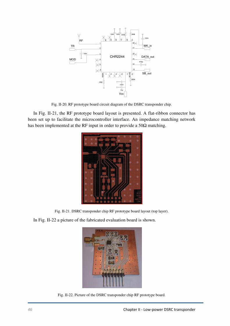
46 Chapter II - Low-power DSRC transponder
Fig. II-20. RF prototype board circuit diagram of the DSRC transponder chip.
In Fig. II-21, the RF prototype board layout is presented. A flat-ribbon connector has
been set up to facilitate the microcontroller interface. An impedance matching network
has been implemented at the RF input in order to provide a 50Ω matching.
Fig. II-21. DSRC transponder chip RF prototype board layout (top layer).
In Fig. II-22 a picture of the fabricated evaluation board is shown.
Fig. II-22. Picture of the DSRC transponder chip RF prototype board.
1
2
3
4
5
6
18
17
16
15
14
13
1211
10987
1920
21222324
CHR2244
RF
TR
MOD
100n
Vcc
2M2
100n
10µ
680k
SE
NS
GA
-SB
SB_out
DATA_out
470p
WK_in
100n
6M8100n 100n 220k

Chapter II - Low-power DSRC transponder 47
After the RF prototype board design and fabrication, we proceed with the chip
characterization, detailed in the next sections.
II.3.2.2. DSRC transponder chip characterization
The chip evaluation board has been tested for the three DSRC operation modes. To
verify the limits of DSRC IC, a characterization setup has been carried out, observing in
particular the transponder response for the following parameters variation: RF input
power signal (power limit communication), modulation bit rate and supply voltage.
Standby mode characterization:
In this mode, an amplitude modulated RF signal is required to produce a DC voltage at
the output SB_out which can be used as a flag of the communication beginnig. SB_out
output is active if and only if an AM modulated signal RF is applied at the RF input. The
standby characterization setup is presented in Fig. II-23.
Fig. II-23. Standby characterization setup (control commands: T/R=0 , MOD=0 , WK_in=0).
If the RF input signal is detected by the transponder chip, a DC voltage is produced at
the SB_out output during the communication frame, as shown in Fig. II-24.
Fig. II-24. Oscilloscope print screen of the SB_out output during a successive AM signal receiving.
RF input signal variation: for the four DSRC carries frequencies (5.7975GHz,
5.8025GHz, 5.8075GHz, 5.8125GHz) the RF input signal varies from -50dBm to 0dBm,
the modulation bit rate is set to 500kbit/s and the supply voltage to 3.1V. The IC
transponder has responded well for all RF powers, i.e., a clear DC signal on the SB_out
output has been detected. During the measurements, the standby DC current has been
found to be approximately 9µA.
Generator : 5.8 GHz AM signal CHR2244
RF SB_out Oscilloscope

48 Chapter II - Low-power DSRC transponder
Modulation bit rate variation: for this measurement, the RF input signal level is set to
-30dBm (typical DSRC RF input power), the carrier frequency equals 5.8025GHz and the
supply voltage is 3.1V. The modulation bit rate has been varied from 31.25kbit/s to
530kbit/s and the IC transponder has reacted well, by presenting a clear DC voltage on
the SB_out output. For a bit rate of 100kbit/s, which is not of our interest, the result is not
stable.
Supply voltage variation: In order to verify the supply voltage limitation of this IC, we
have varied the Vcc from 2.7V to 3.6V and set the RF input signal level to -30dBm. The
carrier frequency equals 5.8025GHz and the modulation bit rate 500kbit/s. During this
variation, the circuit has worked at all voltages (no problems were detected).
Downlink mode characterization:
During the downlink mode, additionally to the SB_out output, we have the DATA_out
output active. The received data is demodulated and accessible at the DATA_out. The
downlink characterization setup is presented in Fig. II-25.
Fig. II-25. Downlink characterization setup (control commands: T/R=0 , MOD=0 , WK_in=Vcc).
The RF input signal applied this time is a typical DSRC frame, as described in [121].
The frame has been sent continuously during the measurements. Fig. II-26 shows the
oscilloscope print screen, where the rose curve is the SB_out signal and the yellow curve
is the DATA_out signal. We can observe that both outputs are synchronized. The SB_out
confirms the frame begin and end.
Fig. II-26. Oscilloscope print screen of the downlink mode setup measurement.
Generator : 5.8 GHz DSRC frame CHR2244
RF SB_out Oscilloscope
DATA_out
Oscilloscope

Chapter II - Low-power DSRC transponder 49
In Fig. II-27, a zoom on a frame is presented. The yellow curve (DATA_out) shows a
wake-up preamble before the frame, and then the flag (rose curve, SB_out) presents a
rising edge signaling that the frame starts. At the frame end, since there is no amplitude
variation on the data, the flag shows a falling edge.
Fig. II-27. Oscilloscope print screen of the downlink mode – frame zoom.
As for the standby mode, a measurement setup has been developed in order to push the
IC transponder to its operation limit, by applying the same parameter variation (supply
voltage, frequency carrier and bit rate). During the downlink measurements, the IC
responded well for the parameter variation, the only difference being that the current
consumption evidently increased to 159µA due to the operation mode changing (standby-
>downlink).
Uplink mode characterization:
Uplink mode relies on a backscattering of the incoming carrier 5.8GHz ( ) multiplied
by the modulated data ( ) at the input MOD. In fact, the ETSI standard recommends the
modulation to be made around a subcarrier . The uplink signal result is a transposition
of the carrier around the sub-carrier ( ± ), as presented in Fig. II-28.
Fig. II-28. Uplink spectrum is a result of a transposition of the carrier around the sub-carrier.
The characterization setup for the uplink mode requires an extra attention, since we
need to inject the carrier signal, multiply it with the modulated data and then observe the

50 Chapter II - Low-power DSRC transponder
spectrum to verify if the modulation is corrected. Fig. II-29 shows the characterization
setup for the uplink mode.
Fig. II-29. Uplink characterization setup.
At the MOD input we should provide the subcarrier at 1.5MHz or 2.0MHz which itself
is phase modulated with the uplink data stream (250kbit/s). For this reason, we set up a
BPSK modulator based on a synchronization of the sub-carrier ( ) and the data ( )
signals in a XOR gate, as described in Fig. II-30.
Fig. II-30. BPSK modulator based on a synchronization of the sub-carrier (fM) and data (BBS) signals through a XOR gate
The signal generator we have use is the Tektronix AFG3011 Arbitrary Function and
the XOR gate is the ST HCF4030B. The sub-carrier and data frequencies are 1.5MHz and
250kHz, respectively. In Fig. II-31 a print screen of the BPSK modulator signals is
presented.
Fig. II-31. Oscilloscope screen picture of the of the BPSK modulator signals.
With the BPSK modulator conceived, we have performed the uplink characterization
setup as described in Fig. II-29. In Fig. II-32, we show the uplink spectrum, with the
carrier signal (center pick) and the modulation on the sub-carrier signal (two laterals
signals).
fM
BBS
fM(1.5 MHz)
BBS (250 kHz)
BPSK signal Phase shift
MOD
Generator: 5.8 GHz carrier
CHR2244
Spectrum analyzer
BPSK Signal (sub-carrier)
Circulator

Chapter II - Low-power DSRC transponder 51
Fig. II-32. Spectrum analyzer screen picture of the uplink spectrum signal.
The DSRC transponder chip characterization has provided corrected results, and
therefore, we have decided to integrate this IC in our DSRC transponder.
II.3.3. Microcontroller sleep mode + Demod Bloc (FPGA)
As presented in previous sections, the DSRC chip has three operation modes: standby,
downlink and uplink. In general, the transponder remains in standby mode and only when
the vehicle is approaching an e-toll plaza, it switches to the active operation mode. A
considerable energy saving could be achieved if we could just turn on the DSRC chip
when the car starts to move for example. Given that we need an extra operation mode
with very low power consumption and from a wake-up flag, the transponder switches on
to the classical standby-by mode.
Since the microcontroller supplies and pilots each bloc of the DSRC transponder,
choosing a low power microcontroller with a deep-sleep mode is primordial.
Nowadays we can find microcontrollers that provide a deep-sleep mode for very low
power consumption. The C8051F91X from Silicom labs provides a deep-sleep mode that
consumes 50nA, and an active mode consuming 160µA/MHz (24.5MHz clock).
Recently, Microchip has presented the nanoWatt microcontroller series providing a very-
low-power deep-sleep mode. The PIC1XF182X Microchip family achieves sleep currents
as low as 20nA, and a run mode current consumption less than 50 A/MHz. Moreover,
Microchip has presented the PIC24F16 with deep-sleep mode current down to 20nA and
run mode current down to 8µA. We choose the PIC24F16 from Microchip for our DSRC
transponder design.
Although the very low-power microcontroller was chosen, during the downlink mode,
the DSRC transponder needs to demodulate a 500kbit/s AM signal. Given that a potential
DEMOD bloc will be need in order to help the low-power µC to process the received
information. This bloc could be implemented by a FPGA. In this thesis, the DEMOD bloc
is not analyzed, but it is included in the transponder diagram.
II.3.4. A new deep-sleep mode
To the best of our knowledge, the DSRC transponders currently available on the
market have tree operations mode: standby, downlink and uplink. From the electric power

52 Chapter II - Low-power DSRC transponder
consumption results obtained in section II.3.1, we have observed that during a day the
operation mode that consumes more energy is the standby mode. In this thesis we thus
propose a new low-power standby mode, i.e., a deep-sleep mode.
Depending on the driver’s profile, the vehicle use differs. For instance, highways
drivers, often make pauses for rest during the day and, in general, keep their vehicles
parked during the night; in a common day-to-day city life, the duration for which the
vehicle is parked is bigger. Average number of kilometers per year in France is around
25,000km (about 68.5km/day), so less than 2 hours of use by day and 22 hours of
parking. For most DSRC transponders available today, during all this “parking time” the
DSRC transponder is running in standby mode (13µA/3.6V).
For the DSRC transponder proposed in this thesis, while the vehicle is parked, the
transponder is in a (very-low-power) deep-sleep mode and only when the motor is turned
on, it switches to the standby mode. This wake-up will be induced by a vibration sensor.
The new operation mode for the DSRC transponder is presented in Fig. II-33.
Fig. II-33. The new low-power statechart for the DSRC transponder.
The vibration sensor chosen for our application is the SQ-MIN-200 produced by
Signal Quest [122]. The SQ-MIN-200 is an omnidirectional sensor that acts as a closed
switch in the rest state and chatters open/closed when it is tilted or vibrated. Hence, we
can define our DSRC transponder by a five bloc structure as presented in Fig. II-34. An
additional DEMOD bloc is inserted in our diagram in order to help the microcontroller
demodulating a 500kbit/s signal.
Fig. II-34. Low-power DSRC transponder schema bloc.
Deep-Sleep
Vibration
Δt + VibrationDownlink
Standby
Uplink
BST_received
Δt + DATA
DEMOD_OK
END_linkEND_link
BST_received
Vibration sensor
DEMOD blocDSRC chip
µC
Antenna

Chapter II - Low-power DSRC transponder 53
A detailed flowchart for the low-power DSRC transponder is presented in Fig. II-35,
illustrating each condition for the mode transition and the respective powered blocs.
Fig. II-35. Flowchart of the low-power DSRC transponder.
II.3.4.1. Vibration sensor evaluation board design
In a simple configuration, the vibration sensor requires only a resistor to limit current,
and is fully passive. For our application, a sensitivity control circuit (or lowpass filter)
should be employed to reject light vibration/bumps and to provide a proper trigger; an
integrating capacitor is used to determine the integration time. Since the wake-up signal
from the vibration sensor goes directly to the microcontroller, it is important to keep a
minimum voltage amplitude, in order to ensure the wake-up signal is detected by the µC.
Nevertheless, the current consumption of the sensor is proportional to the supply voltage
Flowchart low-power DSRC transponder
MO
DU
LES
Standby Downlink UplinkDeep-sleep
Vibration Sensor
Vibration?
µController
Vibration sensor: ONµController: ONDSRC chip: OFFDEMOD bloc: OFF
DSRC chipdeep-sleep/standby
µController
AM Signal?
Vibration sensor: ONµController: ONDSRC chip: ONDEMOD bloc: OFF
Vibration sensor: OFFµController: ONDSRC chip: ONDEMOD bloc: ON
Vibration sensor: OFFµController: ONDSRC chip: ONDEMOD bloc: OFF
DSRC chipstandby/downlink
DEMOD OK?
µController
DSRC chipdownlink/uplink
Δt + Vibration
END_LINK?
YESNO
DEMOD bloc
YESNO
NO YES
NO YES
YESNO

54 Chapter II - Low-power DSRC transponder
applied on its terminals. Another important point is that the sensor is sensitive to the
mounting position (vertical, horizontal, diagonal …) and the direction of the excitation.
Based on the above specifications a sensor prototype board has been designed and
realized in order to test the sensor sensitivity in an in-situ configuration (II.3.4.2). In Fig.
II-36, the circuit diagram of the vibration sensor prototype board is presented. Two
sensors have been deployed on two perpendicular directions on the evaluation board. At
the circuit input, different series resistor values are added to provide a flexible resistance
during the tests. An integrator capacitor of 5nF is used. The simplified circuit diagram is
presented in Fig. II-36. Cap_out1 and Cap_out2 are the outputs interface to the µC.
Fig. II-36. Circuit diagram of the vibration sensor prototype board.
For the sensor prototype board layout an interesting assembly has been achieved. Since
the evaluation board is controlled by a microcontroller, during the in-situ tests, it is
interesting to reduce the number of the equipments on board (inside the vehicle). From
the already available microcontroller board, we have designed the sensor board in order to
match the supply voltages pins of the microcontroller board. To yield a better mobility for
the assembly, the supply voltage has been provided by a USB port (+5V) from the laptop
used during the measurements. Therefore, at the circuit input a zener diode is required in
order to assure +1.8V to the microcontroller supply. Three LEDs have been deployed
with the purpose to indicate the output information: one for the supply voltage indication
and two others for vibration detections (horizontal and vertical vibration sensors).
In Fig. II-37 the layout of the vibration sensor prototype board is presented. A picture
of the assembly (sensor + microcontroller board) is shown in Fig. II-38
5n
47
10M
5M
2M
2M
VibraSensor01VibraSensor02
Vcc
Cap_out1
10M
5M
2M
2M
Vcc
5n
47 Cap_out2

Chapter II - Low-power DSRC transponder 55
Fig. II-37. Vibration sensor prototype board layout.
Fig. II-38. Picture of the assembly (sensor + microcontroller board).
II.3.4.2. In-situ deep-sleep tests
The aim of the in-situ tests is to verify if the vibrations induced by the vehicle
movement could be detected by the vibration sensor. We are also interested in verifying
how the vibration sensor responds for different vehicle movements/actions (starting the
car, closing the door, acceleration …).
The assembly (vibration sensor prototype board + µC board) is fixed on the windshield
of the vehicle in a specific position , that is, one of the sensors is in a horizontal position
relative to the ground and the other one in a vertical position. To check if the vibration
sensor responds correctly, different scenarios have been tested, the vibration detection
criterion being based on the LED lighting as following:
OK+: LED lighting was constant, i.e., strong vibration detected.
OK: LED lighting was shortly observed, i.e., light vibration detected.
NOK: No LED lighting observed, i.e., no vibration detected.
The measurement results are presented in Table II.8.

56 Chapter II - Low-power DSRC transponder
TABLE II.8. VIBRATION SENSOR IN-SITU MEASUREMENTS RESULTS.
Actions Vibration sensor 01
(horizontal) Vibration sensor 02
(vertical)
Closing the door OK+ OK+
Starting the car OK OK+
Vehicle initial acceleration OK OK+
Constant speed in a city OK OK+
Constant speed in a high-way (110 km/h) OK OK+
Curves OK+ OK
Vehicle stopped at a traffic light NOK NOK
Both sensors are appropriate and sensible for different scenarios and very precise even
when the vehicle has stopped at a traffic light. As expected, the mounting position
influences the vibration detection. An interesting scenario to exemplify the importance of
the mounting position is when the vehicle is in a curve, since the horizontal sensor
responds better than the vertical one, as shows Table II.8. Nevertheless, both
(vertical/horizontal) mounting positions have provided satisfactory results. The electric
power consumption measurements have been also analyzed, but they are described in the
next section with total amount of DSRC transponder power consumption.
II.3.5. The energy consumption of the proposed DSRC transponder
From the different blocs proposed for the new DSRC transponder in Fig. II-34, we
have the following supply voltage range values accepted, based on the datasheet of the
manufactures:
Vibration sensor: 0.9V - 12V
DSRC chip: 2.7V – 3.6V
Microcontroller: 1.8 to 3.6V
DEMOD bloc: not yet performed
Since the microcontroller provides the for the others blocs, we have decided to
supply the microcontroller with +3.3V and thus +3.1V will be available to the other blocs.
The microcontroller chosen for our application is the nanoWatt Microchip PIC, which has
a very-low-power current in the deep-sleep mode, [123]. Table II.9 shows the total
electric power consumption for the low-power DSRC transponder proposed in this thesis.
TABLE II.9. TOTAL POWER ELECTRIC CONSUMPTION FOR THE NEW LOW-POWER DSRC TRANSPONDER.
Module/Operation mode Deep-sleep Standby Downlink Uplink
Vibration sensor (+3.1V) 164nA* 164nA* OFF OFF
DSRC chip (+3.1V) OFF 9µA* 159µA* 159µA*
µC (+3.3V) 20nA# 2µA# 8 A# 8 A#
*Measured values, # theoretic values.
We can take the example of the city driver, who goes to work and needs to use the
highway traversing two DSRC toll plazas. We consider that he needs one hour to go to
work and one to come back home and that during the night his vehicle is parked.

Chapter II - Low-power DSRC transponder 57
Following the power electric consumption measurements (Table II.9) and based on the
flowchart presented in Fig. II-35, we can estimate the energy required by the DSRC
transponder for each operation mode during a day. Table II.10 shows the estimated
amount of energy required by the new DSRC transponder during a day.
TABLE II.10. ENERGY REQUIRED BY THE NEW DSRC TRANSPONDER DURING A DAY.
Operation mode Current Duration Energy
Deep-sleep 184nA ~22h 48mJ
Standby 11.2µA ~2h 266mJ
Active (down and up link) 167µA ~200ms (4times e-toll passage) 0.1mJ
TOTAL 0.18mA 24h 314mJ
With the proposed statechart, it is clear that the current consumption can be
considerably reduced, by using to the new deep-sleep mode. Since the deep-sleep needs
48mJ during a day and it is the predominant mode, the total power consumption of the
transponder is significantly reduced. In the next section, we compare the power
consumption of the DSRC transponder proposed in this thesis with the power
consumption of others transponders.
II.4. Conclusions
In this chapter we have presented the proposed new DSRC transponder with an
original statechart that considerably reduces the power consumption.
First of all, the DSRC system has been introduced and then the RF link budget
modeling has been carried out in order to predict the best DSRC mounting configuration.
Since we did not have any knowledge about the amount of energy the transponders on the
current market consume, we have established our own measurement setup to acquire this
information. Based on these measurements, we have designed a low-power DSRC
transponder.
The new DSRC transponder design starts with the DSRC chip characterization, for
which an evaluation board has been conceived to assist the measurements. Since the IC
measured performance corresponds well to our specifications, we have decided to include
the DSRC chip in our transponder design. We have implemented a deep-sleep mode
based on a vibration sensor, and a mobile evaluation board supplied by a USB port has
been conceived. In-situ tests have been carried out. By implementing the supplementary
operational mode, the electric power consumption has been considerably reduced.
Coming around the example of the driver described previously, that is, spending two
hours per day on the road and keeping its vehicle parked during the night, a comparative
table between the classical and the proposed DSRC transponder in this thesis is described
in Table II.11. Reminding that classical transponders do not have a deep-sleep mode and
that the standby mode is predominant during a day, our approach makes major use of a
deep-sleep mode.

58 Chapter II - Low-power DSRC transponder
TABLE II.11. ENERGY CONSUMPTION COMPARISON BETWEEN THE CLASSICAL AND THE PROPOSED DSRC
TRANSPONDER IN THIS THESIS
Operation mode Classical Transponders Transponder proposed
on this thesis
Deep-sleep --- 48 mJ
Standby 4 J 266 mJ
Active (down and up link) 6.5 mJ 0.1 mJ
Total (24 h) ~4 J ~314 mJ
From Table II.11, a factor of 13x concerning the energy consumption per day is
identified when comparing classical DSRC transponders and the one proposed in this
thesis.
The feasibility of recharging the battery of the DSRC transponder by means of
Wireless Energy Harvesting has been discussed in section II.2.2.2. The amount of RF
energy harvested by the DSRC transponder for the two DSRC e-toll cases (Free-Flow and
Stop&Go) has been estimated using the RF link budget. The RF energy harvesting could
become attractive to power the transponder only for Stop&Go configurations (stop
time>2s). An amount of energy of 10 µJ could be recovered if the driver spends 2s in the
RSE antenna field. Nevertheless, even if considering the transponder power consumption
proposed in this thesis (314mJ), the recovered energy by means of DSRC Wireless
Energy Harvesting would not be enough. Moreover, the request that the vehicle should
spend more time in front of the antenna counteracts the DSRC toll collection principle,
that is, reducing traffic jams and time spent in highway tolls. Based on this analysis, we
have decided to explore the Wireless Energy Harvesting for other than the DSRC 5.8GHz
frequency, we chose therefore, the 2.45 GHz that is also included in the ISM band
(Chapter IV).

Chapter III – Antenna design 59
Chapter III - Antenna design
III.1. Introduction
Nowadays antennas gain their place everywhere in environments surrounding us.
Television, radio, cell phones, WiFi, garage doors opener, car remote locking central, etc,
are just a few examples of applications that require antennas for functioning. Antennas
are indispensable for any radio receiver or transmitter to couple its electrical connection
to the electromagnetic field.
The first antenna was built by the German Heinrich Hertz in 1888. He developed a
wireless communication system in which an electrical spark was forced to occur in the
gap of a dipole antenna [124]. Nevertheless, we could associate the terminology creation,
“antenna”, with the Italian Guglielmo Marconi, in 1895, in the Swiss Alps, he conceived
an early radio communication between two long wires that he named “aerials”. Marconi
uses the word antenna that spreads among wireless researchers, and later is adopted by
the general public [125]. Antenna or aerial could be defined as “a means for radiating or receiving radio waves”, in IEEE Standard Definitions of Terms for Antennas [126]. In
other words the antenna is an interface between free-space and guiding device, as defined
in [127]. A good review about major events in the development of antennas is presented
in [128].
In this chapter, we describe the fundamentals of antennas, basic definitions,
highlighting the different field regions around the antenna. Then, in III.3, we present the
Multitoll requirements for the antennas design, followed by the detailed explanation of
the antennas developed in this thesis: in III.3.3 for DSRC applications and in III.3.4 for
Wireless Energy Harvesting.
As already explained in the introduction of this manuscript, this thesis was realized in
collaboration between the IMEP-LAHC laboratory and the Multitoll Solutions SA
Company. Consequently some of the antennas have been designed following rigorous
specifications from Multitoll, applying to specific practical applications. Nevertheless, an
important effort was devoted in order to promote the transfer of knowledge from research
to the industry.
III.2. Antenna fundamentals
III.2.1. How an antenna radiates
Let us take the simple case where two conductor wires are connected to an antenna and
are excited by a source, as shown in Fig. III-1. Since a voltage is applied across the
conductors, an electric field is generated between the conductors. Nevertheless, the
radiation occurs if there is a movement of charge, i.e., creation of the current that in turn
creates a magnetic field intensity. If there is no motion of charges, no radiation arrises. In

60 Chapter III – Antenna design
order words, due to the time-varying electric and magnetic fields between conductors, the
electromagnetic waves travel along the transmission lines and when approaching open
space, the radiation occurs, as shown in Fig. III-1(b).
If we assume the voltage source is sinusoidal, electromagnetic waves are created
continuously with a period equal to that of the applied source, and these waves travel
along the transmission line, throughout the antenna and are radiated into free space.
Inside the transmission line and the antenna, the electromagnetic waves are sustained due
to the charges, but as soon as they enter the space, they form closed loops and are radiated
as described in [127].
Fig. III-1. Antenna radiation example (source, transmission line, antenna and free-space propagation). (from [127]).
The two-wire conductor is one example of antennas. It is useful to explain the electric
and magnetic field variation that generate the radiation.
III.2.2. Fundamental parameters of Antennas
III.2.2.1. Radiation pattern (farfield)
The antenna radiation pattern is defined by IEEE standard as “the spatial distribution
of a quantity which characterizes the electromagnetic field generated by the antenna” [129]. In other words, the radiation pattern describes the relative strength of the radiated
field in different directions. In general, the radiation pattern is determined in the farfield
region. Various plotting formats to represent a radiation pattern exist: Cartesian plot (Fig.
III-2), polar (Fig. III-3(a)) and 3D plot (Fig. III-3(b)). A radiation pattern is composed of
several lobes, which may be classified into main, side and back lobes, as described in Fig.

Chapter III – Antenna design 61
III-2. The main lobe is the lobe which determines the direction of maximum radiation.
The side lobes are the lobes in any direction other than the main lobe, and in general, are
adjoining to the main lobe. The back lobe is the symmetric (180°) of the main lobe, i.e.,
the back lobe is oriented in the opposite direction of the main lobe. In most of
applications the requested ratio between the main lobe and the side lobe is around -20dB.
Fig. III-2. Radiation pattern in Cartesian plot.
(a) (b)
Fig. III-3. (a) Radiation pattern in polar plot. (b) Radiation pattern in 3D plot.
III.2.2.2. Beamwidth
The common definition for the beamwidth is the angular distance created from the
main lobe peak to the two points on either side corresponding to the half power (-3dB).
For this reason the half power beamwidth (HPBW) is sometimes referred to as the 3dB
beamwidth. In Fig. III-3, the beamwidth is represented (blue lines) in polar form.
However, we can also present it in Cartesian form.
III.2.2.3. Return loss and reflection coefficient
Return loss is basically a logarithmic ratio of relative magnitudes of input power ( )
and reflected power ( ):
Main lobe
Side lobe
Back lobe

62 Chapter III – Antenna design
(III-1)
The name “loss” comes from the fact that the reflected power cannot exceed the input
power; consequently , and should be a positive number.
The S11 parameter, or reflection coefficient, also expressed in dB, is the opposite of RL
(negative values)
Reflection coefficient:
Reflection coefficient (Γ) is defined as the ratio of the reflected wave to the
incident (or forward) wave. The quantity of interest (magnitude of the reflected
wave) is compared to the initial quantity (magnitude of the forward wave):
(III-2)
Since , the reflection coefficient is always . This coefficient has a link
direct with the S11 parameter, through the ABCD matrix of S parameters.
III.2.2.4. Bandwidth
The bandwidth of antenna may be defined as “the range of frequencies within which the performance of the antenna, with respect to some characteristics, conforms to a
specified standard” [127]. From the center frequency, the range of frequencies which the
antenna characteristics (radiation pattern, polarization, input impedance…) are comparable to those of the center frequency, this is the antenna bandwidth. In general, the
antenna bandwidth is given in percentage, e.g., a 3% bandwidth indicates the range of
frequencies where the antenna performance is still acceptable compared to the center
frequency.
III.2.2.5. Antenna efficiency
The total efficiency describes how much of the power provided to the antenna is
radiated or lost within the antenna. The total efficiency can be expressed as a percentage
or in decibels. The total efficiency ( ) should take into account the dielectric efficiency
( ) (losses due to dielectric material), conduction efficiency ( ) and reflection mismatch
efficiency ( ), as follow:
(III-3)
III.2.2.6. Gain
The antenna gain describes how much power is transmitted in the direction of peak
radiation to that of an isotropic source, and it is in general represented in dBi [127]. The
absolute gain ( ) is the total efficiency multiplied by the antenna directivity (D):
(III-4) All simulation results of the antenna gain presented in this thesis are extracted from the
CST Microwave Studio software. However, in this software the antenna gain (“realized gain”) is given in dB.

Chapter III – Antenna design 63
III.2.2.7. Polarization
The antenna polarization can be defined as the emplacement relation of the traced by
the extremity of the time-varying field vectors at a fixed observation point. In other
words, it describes the behavior of the field vectors (direction and magnitude) change
over time.
Depending on the instantaneous plane wave behavior (electric field vectors position),
traveling in a z direction in a farfield zone, the polarization can be classified as linear,
circular or elliptical. If the electric field at a point in space as a function of time is always
a line, this characterizes a linear polarization. If the X and Y electric field components are
90° out of phase and have the same amplitude, the wave plane seen is a circle, namely a
circular polarization. Finally, if electric field vectors are two perpendicular components
and out of phase with 90 degrees, but not equal in magnitude, this defines an elliptical
polarization. However, in practice there are no perfect linearly or circularly polarized
antennas, the antennas are often elliptically polarized.
Fig. III-4 shows an example of the electric field polarization distribution, for an
elliptical polarization.
Fig. III-4. Ellipse polarization.
Fig. III-5 shows how the electric field vectors impact the polarization, considering
their amplitude ratio and phase delay. The ellipse may be represented by the Axial Ratio
(AR), the ratio of the two main axes and its tilt angle. The perfect value of the axial ratio
for circularly polarized fields is 0dB, when the components have equal magnitude and are
90 degrees out of phase.
εy
εxzMajor axis
Minor axis
Êy
Êx

64 Chapter III – Antenna design
Fig. III-5. Polarization as a function of Ey/Ex magnitude ratio and phase angle. Figure extracted from [130]
In a radio communication link budget between two antennas Rx and Tx (e.g., DSRC,
RFID, Television, radio…), the antenna polarization plays an important role. In practice,
the polarization of the receiving antenna is rarely exactly the same as the polarization of
the incoming wave. This polarization “mismatch” is named the Polarization Loss Factor
(PLF) and is defined as follows [127]:
(III-5)
where is the unit vector of the incoming wave, is the polarization vector of
the receiving antenna and is the angle between the two vectors (Ey/Ex). PLF is
dimensionless.
From (III-5), if the antenna is polarization matched, the PLF is equal to one, i.e., the
receiving antenna extracts the maximal power from the incoming plane wave. In Table
III.1 an interesting comparison of the PLF for different polarization patterns, including
different antenna types is presented.
TABLE III.1. POLARIZATION LOSS FOR VARIOUS ANTENNA COMBINATIONS. TABLE EXTRACTED FROM [130]
III.2.3. Near and Far field regions
When measuring antenna radiation pattern or calculating RF link budgets using the
Friis power transmission formula, the first underlying criterion is if the Tx and Rx

Chapter III – Antenna design 65
antennas are sufficiently far enough from each other to be considered in the far-field. In
[132]-[133] the distance that Tx/Rx should respect for the farfield region is defined by:
(III-6)
where is the maximal linear dimension of the antenna and is the operating
wavelength.
However (III-6) is correct if and only if the following criteria are respected:
and , as reported in [134].
The space surrounding an antenna is usually divided into three regions [127]: (a)
reactive nearfield, (b) radiating nearfield (Fresnel) and (c) farfield (Fraunhofer), as shown
in Fig. III-6.
Fig. III-6. Field regions around an antenna showing the typical changes of antenna amplitude pattern.
Reactive nearfield:
In this region, the reactive power density dominates. It is the region that immediately
surrounds the antenna. The outermost boundary of this region is at a distance where is the distance from the antenna surface, is the largest
dimension of the antenna and is the wavelength.
Radiating nearfield (Fresnel):
Fresnel region is the transition zone between reactive nearfield region and farfield
region. In this region the reactive power density becomes lower than the radiating power
density. The field pattern has a conventional shape, i.e., its shape is a function of the
radial distance, as described in Fig. III-6. The outermost boundary for this region is at a
distance where is the distance from the antenna surface.

66 Chapter III – Antenna design
Farfield (Fraunhofer):
This region is defined as “that region of the field of an antenna where the angular field
distribution is essentially independent of the distance from the antenna” [127]. The RF
power density varies with the inverse square of the radial distance in this zone. The inner
boundary is at the radial distance and the outer one at infinity. In the
Fraunhofer region, the pattern is well formed and has, in general, a few minor lobes and
one, or more, major lobes, as described in Fig. III-6. In the farfield zone, only the
radiation fields exist, the reactive fields are absent.
III.2.4. Different antenna types
Many the antenna types are available in the literature, and the choice of the antenna
should be made depending on the final application. In additional to the classical role, of
receiver and emitter, in advanced wireless systems the antennas could be employed to
suppress or accentuate the radiation energy in a specific direction, and in other cases, the
antenna would be used as a simple probing device. In this section, some of the commonly
used antennas are briefly described.
Let us start with the dipole; it has been widely studied [135]-[138]. In general, dipoles
are composed of two branches each one of a size of /4. Consequently the propagating
wave in a dipole travels a total of /2 from the initial point. The typical directivity of the dipole is 2.23dB and the bandwidth is of about 10% [134].
Another inexpensive and versatile antenna is the loop antenna. Loop antennas are
characterized by a “loop” of wire or other conductor that is connected to a balun [139]-
[143]. There are two categories of loop antennas: electrically small when the antenna size
is smaller than a wavelength (magnetic loop), and electrically large when the antenna size
is approximately equal to a wavelength (resonant loop). Most of the applications for loop
antennas are between the HF (3-30MHz) and UHF (300-3000 MHz). Loop antennas can
be also used as a “probe” device, as described in [143]. Helical antennas is an easy way to
obtain a good circular polarization (excited on axial mode), but they are difficult to
fabricate.
The helical antenna was first described by John Daniel Kraus [144], and it is still
employed for different applications [145]-[147]. A particular antenna shape gained an
important attention last decades, which we call fractal antennas. In fact, the fractals have
their in mathematics. First described by Benoît Mandelbrot in 1975 as a way of
classifying structures where dimensions are not integer numbers, fractals have an unique
geometry that occurs in nature. It can be used to describe tree leaves, plants branching,
rough terrain, coastline jaggedness, and many other natural elements. However, lately its
potential for antenna design was recognized [148]-[157]. It was observed that the fractals
radiate electromagnetic energy in an efficient way and with a multiband behavior, i.e.,
they can radiate multiple wavebands signals when their properties of impedance are
compared with those of the Euclidean antennas having the same total size. In [158] and
[159], two different fractal shapes (Koch Island and Sierpinski Gasket) were applied for

Chapter III – Antenna design 67
the RFID antenna design. Finally, the most deployed antenna type in different
applications is the microstrip antenna, which is described in detail in the next section,
pinpointing its advantages and disadvantages.
III.3. Antenna design
III.3.1. Multitoll antenna specifications
As Multitoll is one of the worldwide turn-key leaders of e-toll solutions, they provided
us with the antenna specifications for the DSRC application. These requirements should
be rigorously taken into account, since the antennas developed in this thesis are deployed
in real applications under protocol regulations. The specifications were the following:
Low-cost antenna, easy to fabricate and that may be rapidly tested in a real in-
situ test.
Antenna gain: RSE 13-15 dBi and OBU 5-6 dBi
Antenna bandwidth respecting the DSRC standard: 5.795-5.815 GHz (20MHz)
A minimum S11 parameter of -10dB over all the bandwidth
Left-hand circular polarization
Technology should be microstrip
III.3.2. Microstrip antenna
Microstrip radiators were first described by Deschamps in 1953 [160]. However, only
some decades later, in 1970, microstrip antennas were fabricated [161]-[173]. This
development accelerated due to the availability of good substrates with low loss tangent
and attractive thermal and mechanical specifications. Nowadays, microstrip antennas are
fully deployed in different fields and frequencies, due to their numerous advantages, e.g.,
easy large-scale fabrication, compatibility with integrated circuits, simple and
inexpensive manufacturing using modern printed-circuit technology, low weight, low
cost, and so on. A good review of microstrip antennas can be found in [174]-[186].
Microstrip antennas are attractively versatile, since the radiator elements can be loaded
with lumped elements (e.g., pins and varactor diodes), providing a frequency and/or
polarization and/or pattern variation [187]-[192].
A microstrip patch antenna consists in a conductor metal shape (rectangular, circular,
ellipse, triangle…) on one PCB face and the ground plane on the other side. Typically, a
patch antenna has a gain between 5 and 8 dBi and a -3dB beamwidth between 70° and
90°. A good review of the radiation pattern characteristics as a function of the metal
shape is presented in [193].
Depending on the application, the feed method has an important role in the antenna
design. Several feeding methods have been reported in the literature, and among them:
microstrip line, aperture coupling and coaxial probe [194]-[200]. Microstrip line feed is

68 Chapter III – Antenna design
more appropriate for the integration with RF circuit (front-end), since all the RF parts can
be directly printed, as shown in Fig. III-7(a). The microstrip line is easy to fabricate and
also to model. Coaxial probe is as well widely used, the inner coaxial conductor is
connected to the radiator and the outer coaxial conductor is connected to the ground, Fig.
III-7(b). However, this method requires more attention for design and fabrication, since
the inner coaxial conductor passes through the substrate, and a parasitic capacitance can
be generated between the inner coaxial conductor and the ground plane. Attention should
be also given to the soldering point on the radiator connecting the inner coaxial
connector, since the radiator surface is sensible to slight electrical modifications. Finally,
aperture-coupled feed is the most difficult to design, Fig. III-7(c). An interesting result of
a dual-fed aperture-coupled circularly polarized patch antenna was reported in [201],
where general practical guidelines for the design of such antennas have been described.
(a) (b)
(c)
Fig. III-7. Typical feed methods for microstrip antennas: (a) microstrip line, (b) coaxial feed and (c) aperture-coupled feed.
Microstrip antennas have been widely used in different applications due to several
advantages intrinsic to their structure. In Table III.2, the most common positive and
negative characteristics of the microstrip antennas are resumed.
WL
hεr
Radiator
Coaxial feed
εr
Slot
Microstrip line feed
Radiator
εr1 εr2

Chapter III – Antenna design 69
TABLE III.2. MICROSTRIP ANTENNAS ADVANTAGES AND DISADVANTAGES
Advantages
Easy large-scale mass production using printed circuit technology leads to a low fabrication cost
Easy integration with other microstrip circuits
Low profile and weight
Linear and circular polarization
Versatile characteristic (varactors, diode…) Disadvantages
Narrow bandwidth
Relative low-gain (~6dB)
Microstrip array need complex feed to achieve high-performances
High mutual coupling within an array environment at high frequencies
Due to these advantages, in this thesis, the different antennas developed are based on
microstrip patch antennas, using two feed methods (microstrip line and coaxial probe
feed). In III.3.3.1, we present the DSRC transponder patch antenna design, that it is
integrated with the DSRC OBU. Then in III.3.3.2, the DSRC reader antenna development
is described, where two different topologies are studied, designed and tested. Finally, in
III.3.4 the patch antenna array designed for Wireless Energy Harvesting applications are
presented.
III.3.3. DSRC antennas
III.3.3.1. DSRC OBU antenna
In Chapter II, the DSRC OBU design is presented, a new low-power mode is described
and the RF front-end is studied and implemented. Nevertheless, to complete the OBU
front-end circuit, Multitoll requested an OBU antenna with a 6dBi gain, left hand circular
polarization, simple to be integrated on the OBU PCB and a maximal occupied area of
20cm2. Given this, we have decide to design a patch antenna fed by microstrip line.
The substrate used is ROGERS RT5880, which has a relative dielectric constant of
r=2.2, a thickness of h=0.787 mm and a tangent loss of tan =0.0009. The antenna design
has been numerically assisted using the antenna analysis software CST Microwave
Studio.
The first step is to match the square patch to the resonant frequency (5.8GHz), by
computation of the physical dimensions (W and L). From Fig. III-7(a), to calculate the
rectangular microstrip radiating patch dimensions, width W and length L, we will apply
the equations (III-7)-(III-10).
The patch width is determined by:
(III-7)
where is the speed of light, is the resonant frequency and is the relative
dielectric constant of the substrate.

70 Chapter III – Antenna design
Due to finite length of this antenna, electromagnetic fields at the edge of the patch
undergo fringing. Thus, to account for the fields present in the air (fringing) and in the
substrate, the effective dielectric constant ( ) is introduced.
(III-8)
where is the substrate height.
For the patch length calculus and also due to the fringing effect, the length of the patch
increases by a distance of 2 :
(III-9)
Finally, the patch length can be computed as following:
(III-10)
Then an impedance transformer microstrip line is designed at the input of the antenna
in order to provide a 50Ω interface. Finally, in order to generate a circular polarization, a well-known method is applied, that consists in triming the ends of two opposite corners of
a square patch [202]. The DSRC OBU antenna is presented in Fig. III-8.
Fig. III-8. DSRC OBU patch antenna.
The S11 simulation results of the OBU antenna are presented in Fig. III-9. A good
matching at 5.8GHz has been achieved, S11=-18dB.
16.85mm
16.85mm

Chapter III – Antenna design 71
Fig. III-9. S11 simulation results of the DSRC OBU antenna
Fig. III-10 shows the simulated radiation pattern of the patch antenna. As can be
observed, a simulated 8dB gain has been achieved (Fig. III-10(a)), due to the low loss
substrate. The patch antenna has a beamwidth of 68.5° (phi=0°, Fig. III-10(b)) and 75°
(phi=90°).
(a) (b)
Fig. III-10. Radiation pattern simulation results of the DSRC OBU antenna: (a) 3D plot and (b) polar plot.
The axial ratio of the antenna is presented in Fig. III-11. As requested by Multitoll, the
OBU patch antenna has to be LHCP (Left Hand Circular Polarization).

72 Chapter III – Antenna design
Fig. III-11. Antenna polarization simulation results of the DSRC OBU antenna.
III.3.3.2. DSRC RSE antennas
In Chapter II, the DSRC link budget is presented, showing the best mounting
parameters for an efficient DSRC system. Among the mounting parameters described, the
RSE radiation pattern has been considered in the RF link budget model. Even though in
the downlink mode (RSE->OBU) the RSE gain is limited by the maximum authorized
E.I.R.P. (+33dBm), on the uplink mode (OBU->RSE), the RSE gain plays an important
role for the receiving signal. Since the OBU is completely reflexive, the uplink signal is
very low, the incoming signal on the RSE needs to be captured by a high-gain antenna.
Multitoll requested two different DSRC antennas: the first one for a specific Stop&Go
application and the second one for Free-Flow applications. The first antenna is a 1x3
patch array with superstrate layers enhancing the antenna gain. The second antenna is a
patch antenna array with 8 elements and an improvement on the circular polarization due
to the sequential rotation feeding.
III.3.3.2.1. Patch antenna array with superstrate
The first DSRC reader antenna requested by Multitoll it is used for a specific Stop&Go
e-toll application. The antenna should be as small as possible, should have a gain so as to
provide a minimum OBU distance detection of 17m from the reader and should be low-
weight. Another condition was that the antenna would be installed in a lateral post, 4m
from the lane, as described in Fig. III-12. Following Multitoll specification, the antenna
gain should be around 14dBi.

Chapter III – Antenna design 73
Fig. III-12. DSRC read antenna Stop&Go mounting configuration.
The preliminary antenna has been designed based on the microstrip patch antenna
theory. The dimensions of the patch are adjusted to ensure a frequency resonance at
5.8GHz. The Rogers RT/Duroid 5880 was chosen as substrate. Then in order to increase
the gain, a 1x3 array has been conceived. The 1x3 patch antenna array is shown in Fig.
III-13.
Fig. III-13. 1x3 microstrip patch antenna array.
Microstrip patch antennas can be fed by a variety of methods, as described previously
in this section. The feed point position has been optimized in order to provide a circular
polarization. The distance between the elements was optimized in order to improve the
antenna gain. For this first DSRC antenna, in order to reduce the “visible antenna surface”, we have decided to implement the feed array on a second layer behind the patch
substrate and, through via connections join the radiators, as shown in Fig. III-14. The
array feeding network has been designed so as provide equal amplitude and phase signal
excitation for each radiating element. In Fig. III-15, a lateral view of the multilayer is
presented.
Fig. III-14. Detailed feeding network lines with via.

74 Chapter III – Antenna design
Fig. III-15. Lateral view of the patch antenna array with via.
The effect of the via-hole diameter has been studied; the via-hole dimensions were
optimized in order to achieve the more suitable response of the antenna return-loss and
circular polarization. The effects of the via-hole radius variation on the antenna
performances are resumed in Table III.3.
TABLE III.3. VARIATION OF THE VIA DIAMETER
Via radius (mm) S11 (at 5,8GHz) Bandwidth (MHz) Total efficiency (%) Gain (dB) AR (dB)
0.5 -18.15dB 206 95 11.45 -2.54
0.64 -20.3dB 210 96 11.49 -1.69
0.75 -22.75dB 220 96 11.51 -0.79
As discussed previously the antenna should be small, nevertheless should present a
high-gain (~14dBi) and with a 1x3 patch array we could achieve this condition. Various
methods are typically used to improve the gain of antennas [203]-[204]. Among them,
superstrate layers method is a useful gain enhancement technique that can be used with
several antennas types and not required specials designs to be implemented, [205]-[206].
The superstrate layers are dielectrics that are placed just above the radiated structure in
order to guide the radiated waves in a certain direction. This concentrates the energy and
increases the directivity. The superstrate layers bend the rays outgoing from the antenna
according to Snell’s law [203], since that the material has positive electromagnetic
properties (µ > 0, ɛ > 0). The dielectric material characteristics used for the superstrate
layers are: ɛ=2.2, µ=1 and tan =0.025. The schema of the patch antenna array with
superstrate is described in Fig. III-16.
Fig. III-16. Patch antenna array with superstrate layers.
Regarding the superstrate layers design, first of all I have optimized the distance (D1)
between the first superstrate layer and the array, and then the distance between layers
Radiating elements
Ground plane
VIA
Feeding network
Top layer
Bottom layer
D2
D1
D2
D2
D2
ε,
ε,
ε,
ε,
ε,
SuperStrate
layers
patch
VIA

Chapter III – Antenna design 75
(D2). Fig. III-17 and Fig. III-18 show the parametric results considering the axial ratio and
gain parameters.
Fig. III-17. Antenna Axial Ratio (AR) and gain based on the D1 variation.
Fig. III-18. Axial ratio and gain based on D2 variation (D1=20mm)
Finally from the parametric assessment results, the best result for D1 is 20mm. For D2
it was observed that the best value of AR is obtained when D2=4mm, and conversely the
gain best value, when D2=6mm. We have decided to chose the AR criterion as more
important in this case, and consequently we have chosen D2=4mm.
In order to highlight the gain enhancement due the use of superstrate layers, we have
compared the simulated gain of the 1x3 patch antenna array with superstrate to the one of
the 1x3 patch antenna array without superstrate; the first is about 13.8dB and second is
about 11.3dB. A gain improvement of about 2.5dB is obtained.
Measurements results:
In order to validate the simulation results, several prototypes have been fabricated.
Nevertheless in this manuscript we restrain the results to only two prototypes.
Unfortunately at the time where we were developing this antenna, IMEP-LAHC
laboratory was not yet equipped with a multilayer printed circuit machine, consequently
the vias could not be directly fabricated. Two different PCBs were fabricated (patch
antennas and feed array), each one with its respective ground plane, and then metallic
wires were used to emulate the vias, connecting the two PCB layers. Next we have
assembled the antenna PCB with the superstrate layers, and finally we have
accommodated the patch antenna array with the superstrate in a mechanical support for
the later fixation on a post for the in-situ tests. Fig. III-19 shows a picture of the final
patch antenna array with superstrate ready for the RF characterization and in-situ tests.

76 Chapter III – Antenna design
(a) (b)
Fig. III-19. Final patch antenna array with superstrate: (a) top view and (b) perspective view of the closed box.
We proceed with the RF characterization of the assembly, the S11 measurements are
presented in Fig. III-20 and compared with the simulation results.
Fig. III-20. S11 measurement results of the patch antenna array.
From Fig. III-20, it is clear that the S11 are not reproducible for both prototypes when
compared with the simulation results.
We pursued the measurements, the maximum gain (boresight) and the AR
(polarization) have been measured and they are presented in Table III.4.
TABLE III.4. MEASUREMENTS RESULTS
Version S11(at 5,8GHz) ∆f (MHz) Gain (dB) AR (dB)
Simulation -24.0dB 220 14 -0.54
Proto I -22.8dB 230 13.8 -5
Proto II -17.0dB 320 13.3 -1
From this preliminary DSRC antenna designed, we can already derive some
conclusions. The measured gain follows the theoretical result. On the other hand, for the
AR and S11 results some issues have been identified. From the fabricated antennas, we
have observed that because of the hand-made via and consequently the different welding
applied, the impedance matching of each prototype is different. The large-scale
fabrication feasibility have been also analyzed and we have concluded that the via could
6.5cm
22.5 cm
10.5cm
-40
-35
-30
-25
-20
-15
-10
-5
0
4,4 4,6 4,8 5 5,2 5,4 5,6 5,8 6 6,2 6,4 6,6 6,8 7
S11
(dB
)
Frequency (GHz)
Simulation
Proto I
Proto II
PCB antenna
Superstrate
Coaxial cable
Foam support

Chapter III – Antenna design 77
be a problem in the fabrication process. Therefore, we have decided to study another
solution for the next DSRC antenna (Free-Flow), which should be easy to fabricate on
large-scale and presents a lower margin of error between the different fabricated
prototypes.
Nevertheless, after the RF characterization of the 1x3 patch array with superstrate
layers, we have proceeded with the in-situ tests in order to evaluate the antenna
performances with the DSRC reader developed by Multitoll. These results are presented
in section III.3.3.2.3.
III.3.3.2.2. Patch antenna array with an improved circular polarization
The second antenna requested by Multitoll, is deployed in Free-Flow e-toll
applications. In Free-Flow e-toll configuration, there is no barrier, no toll booths and no
cash lanes. Motorists instead experience driving on an open highway (multi lanes) with
tolls automatically calculated as they drive through a tolling point, with the only condition
of having an OBU inside their vehicles. In generally, in a Free-Flow e-toll sector, each
lane is equipped with a RSE. In order to avoid the overlapping zone of the contiguous
lobes, the RSE antenna should have a very directional lobe, minimizing the probability of
cross-readings and therefore OBU detection misunderstandings.
Moreover, the RSE radiation pattern should also respect other criteria, imposed by
DSRC standards and also by Multitoll specifications, e.g., the antenna beamwidth should
be 30° (vertical plane) and 15° (Horizontal plane), the side lobe levels should be lower
than -13dB in both planes and the antenna gain should be 15dBi. In addition, the antenna
PCB should occupy a maximum area of 289 x 241mm (radome thickness already
included) since the antenna is further integrated in the DSRC reader box, as shown in Fig.
III-21. Another requirement is that the antenna should resist in an outside environment,
and consequently a radome should be designed and matched with the antenna. Rogers
RT/Duroid 5880 is chosen here as substrate for the antenna.
Fig. III-21. RSE box layout.
The RSE antenna array design starts with the patch element construction. In fact, since
we have already designed a patch element at 5.8GHz for the OBU (Fig. III-8), we have
used this element as start point for this RSE antenna array. The only difference is that for
the OBU antenna design, a 50Ω interface (patch element/front-end) has been carried out,
Radome + RSE antenna area
RSE reader

78 Chapter III – Antenna design
and here, for this RSE antenna array, we conceive the feed network directly connected to
the high impedance microstrip feed line at the patch input. As presented for the OBU
antenna results, the patch element has already a good LHCP, by truncating the corners of
patches. We are interested to preserve and even improve the circular polarization in the
array design. We have applied the sequential rotation feeding [207] that consists in
enhancing the circular polarization of the array, by applying a specific physical rotation
and an electrical delay in each patch element, as described in Fig. III-22. The sequential
feeding involves both the rotation of the antenna feed point and its phase feeding. This
method has the advantage of improving the axial ratio bandwidth and reducing the mutual
coupling between array elements.
Fig. III-22. Sequential rotation array feeding method.
In Fig. III-22, the distances between the patch elements are optimized in order to
obtain lower coupling effects between each element and to improve the antenna gain. For
the feed network design we have applied a particular co-simulation method using the CST
Studio Suite software, with the purpose of reducing the simulation time. The patch
antenna array has been simulated in the 3D CST Microwave Studio environment and the
microstrip feed network has been designed in CST Design Studio, as described in Fig.
III-23. The simulation routine implemented consisted in: first, optimizing the feed
network providing the sequential electrical delay for each patch element and a good
impedance matching, and then the co-simulation (3D environment) in order to obtain the
results (S11 , gain, AR …) of the complete array.
Fig. III-23. Co-simulation method in CST Studio Suite.
40mm
40mm

Chapter III – Antenna design 79
As Multitoll specified, we need to achieve a gain of ~15dBi and a beamwidth of
15°x30°. Consequently, from the antenna array theory, we observe that to obtain a
beamwidth around 15°, we need 4 elements, and for 30° of beamwidth two elements are
sufficient. Finally, we have decided to implement a patch antenna array with 8 elements
in the (2x2)x2 form, as shown in Fig. III-24. It should be noticed that the sequential
rotation feeding method is still applied, but this time, the electrical/physical delay is of
180°, as the bloc of patch elements is doubled.
Fig. III-24. RSE patch antenna array with 8 elements in the (2x2)x2 form.
For the feeding network design, a co-simulation assessment has been also carried out
for the final (2x2)x2 patch antenna array. Finally, after an optimization assessment, the
final RSE patch antenna array layout is presented in Fig. III-25. The receiving and
transmitting antennas have been already assembled on the same PCB in order to check the
coupling effect between the transmission and reception chains. This is a consequence of
the fact that the RSE reader produced by Multitoll has two separated chains Tx/Rx, and
necessarily, two identical antennas. In Fig. III-25, we can observe that on the PCB border
some holes have been done for the fixation.
Fig. III-25. The RSE patch antenna array.
and
180mm
200mm

80 Chapter III – Antenna design
The simulated S parameter results of the RSE antenna are presented in Fig. III-26, S11
and S22 represents the reflection mismatch and the S21 represents the coupling between
antennas (Tx/Rx). The simulated gain and axial ratio are presented in Fig. III-27. The
radiation pattern results being identical for both antennas, we have plotted only once.
Fig. III-26. Simulated S parameters results of the RSE antenna.
(a)
(b)
Fig. III-27. Simulation results of the RSE antenna: (a) gain and (b) axial ratio.

Chapter III – Antenna design 81
From Fig. III-26, a good matching of -18dB for the S11 and S22 is observed as well a
low coupling (-33dB) between the Tx/Rx antenna. From Fig. III-27, a high simulated gain
of 15.8dB is achieved with a good axial ratio for the circular polarization (-1dB).
As discussed previously the DSRC antenna developed in this thesis is part of a
complete DSRC system, and for this reason, some conditions were imposed for the
antenna design (physical dimensions, radiation pattern…) as well as for the box where the
antenna is inserted (Fig. III-21). The antenna PCB should be inserted in a radome box and
the RF sector is isolated from the electronic sector by using a metallic plate, as described
in Fig. III-28.
Fig. III-28. Schema of the radome box.
The radome is composed of a material with a dielectric constant of 2.2 and a thickness
of 5mm. The distance d2 separates the antenna PCB from the radome top layer, and the
distance d1 separates the metallic plate from the PCB antenna. A numerical parametric
assessment has been carried out in order to determine the optimal distance values.
However, each distance variation has been analyzed independently in order to reduce the
simulation time. For d2 variation (10mm to 40mm), a slight S11 deviation has been
observed around ΔS11=0.5dB, and on the antenna boresight, the gain fluctuation is around
ΔG=1dB with the axial ratio variation of ΔAR=0.3dB. Finally, the optimal d2 value found
is 30mm. For the d1 variation (0mm to 30mm), the antenna performances are weakly
affected, within the observed variation ofμ ΔS11=0.3dB, ΔG=0.8dB and ΔAR=0.6dB.
Finally, the optimal d1 value was 15mm.
In order to evaluate the assembly (antenna+radome+metallic plate) and reduce the
simulation time, we have conducted an original simulation process in CST software.
Since we already have the radiation pattern of the patch antenna array alone (Fig. III-27),
by using the import farfield CST tool, we can import the farfield result of the antenna into
the box and then run the simulation with the “Integral Equation Solver”, as shown in Fig.
III-29. By applying this method we reduce the number of mesh, since we do not have
d1 d2
Metallic plate
Antenna PCB
Radome
SMA connector

82 Chapter III – Antenna design
anymore the antenna PCB with its complex feed network, and we considerably decrease
the simulation time (10x).
Fig. III-29. CST simulation method that reduces the simulation time by importing the antenna farfield into the box (radome+metallic plate).
Finally, in Fig. III-30 - Fig. III-32 the simulated results of the RSE antenna for Free-
Flow e-toll applications are presented.
Fig. III-30. S parameters simulation results of the RSE antenna for Free-Flow e-toll applications.

Chapter III – Antenna design 83
(a) (b)
Fig. III-31. Radiation pattern simulation results in polar form of the RSE antenna for Free-Flow e-toll applications: (a) polar with phi=0° and (b) polar with phi=90°.
(a) (b)
Fig. III-32. Simulation results of the RSE antenna for Free-Flow e-toll applications: (a) 3D gain and (b) polar axial ratio.
From Fig. III-30 a good input matching and a low coupling between the antennas
(Tx/Rx) are achieved, of -19dB and -34dB respectively. The simulated radiation pattern
(Fig. III-31) is in good agreement with Multitoll specifications: boresight gain of 16.5dB,
beamwidth of 15.7°x35.4° and a side lobe level of -14.1dB and -12.5dB, for phi=0° and
phi=90° respectively. In Fig. III-32(a) the 3D radiation pattern is presented and in Fig.
III-32(b) the polar axial ratio is presented, which has a value of -1.5dB in boresight
direction, confirming a circular polarization.
Measurements results:
Several antenna prototypes have been fabricated and characterized. Given that, in
general, the measurement results (S parameters, gain, AR) are quite similar between the
prototypes, in this manuscript only results for one prototype are presented. Following
MultiToll strategy and requirements, I was in charge of measuring the performances of
the antenna, without radome and metallic plate. The whole assembly will be characterized
and tested in another time. Fig. III-33 shows the measured S11 parameters results of both
patch antennas array (Tx/Rx).

84 Chapter III – Antenna design
Fig. III-33. Measured S11 parameters results of the both antennas patch array (Tx/Rx).
In Fig. III-34, the radiation pattern measurement results are presented for both
antennas Tx and Rx on two planes (phi equal to 0° and 90°).
(a) (b)
Fig. III-34. Radiation pattern measurement results of both antennas Tx(a) and Rx(b). Red curve is for phi=0° plane and green curve is for phi=90° plane.
From Fig. III-33, a good matching at 5.8GHz can be observed for both antennas Tx
and Rx, -24dB and -27dB respectively. The slight difference on the measured S11 between
both antennas comes from the SMA connector soldering, since the inner coaxial
conductor is connected to the microstrip feed line through a soldering point, as described
in the zoom in Fig. III-35.
5 5.5 6 6.5-30
-25
-20
-15
-10
-5
0
S11 p
ara
me
ter
(dB
)
Frequency (GHz)
Tx antenna
Rx antenna

Chapter III – Antenna design 85
Fig. III-35. Zoom of the soldering point on the microstrip feed line of the antenna array.
In Fig. III-34, the radiation pattern measurement results show good form stability for
both antennas (Tx/Rx). A maximum gain of 14.3dB has been detected in the boresight
direction. Compared to the expected gain (15dB, without radome and metallic plate), the
0.7dB difference is acceptable for an anechoic chamber measurement setup. In Fig.
III-34, the slight inclination of the boresight direction of the radiation pattern
measurements comes from the misalignment of the mounting support of the DUT in the
anechoic chamber. Regarding the side lobe levels, the measurement results are in good
agreement with the side lobe level requested by Multitoll (-13dB). The measured side
lobe levels were -17.5dB (phi=0°, horizontal plane) and -14dB (phi=90°, vertical plane).
III.3.3.2.3. DSRC RSE antennas in-situ tests
The RSE antennas developed in this thesis are part of a complete DSRC e-toll system
conceived by Multitoll. Once the antenna prototypes have been designed, fabricated and
characterized (RF performances) in the IMEP-LAHC laboratory, they were sent to the
Multitoll headquarter in Asnières to proceed the in-situ tests. Multitoll dedicated an
important effort to implement different test scenarios for the validation of the DSRC
system. Two emplacements were used for in-situ tests: a parking space in Multitoll
headquarter for the static tests and the racecourse circuit in Montlhéry for the dynamic
tests. During the tests, three detection systems were deployed: RF, camera and magnetic
loop. These detection systems are necessary to provide enough information to indentify
the vehicle ID. Several parameters have been analyzed, but by far the most important are:
the position of the vehicle on the highway lane, the vehicle speed, the type of OBU, the
type of vehicle (car, motorcycle, truck), the vehicles in an adjacent lane, the detection and
measurement of the static antenna lobe.
In order to present the two DSRC in-situ scenarios, we show the patch antenna array
with superstrate (III.3.3.2.1) under static test (parking) and the patch antenna array with
an improved circular polarization (III.3.3.2.2) under dynamic test (racecourse circuit).
Static test (Multitoll parking):
After the antenna characterization in the IMEP-LAHC laboratory, the first practical
tests are done on the parking of the Multitoll headquarter. The objective of these
Ground gap allowing the inner
conductor SMA passages.
Soldering point

86 Chapter III – Antenna design
preliminary tests is to evaluate the antenna performances when connected to DSRC
reader. In Fig. III-36, a picture of the static tests site is presented.
Fig. III-36. Parking of the Multitoll headquarter used for the static DSRC tests.
The patch antenna array with superstrate has been developed for a specific Stop&Go
application. In order to implement the mounting configuration, described in Fig. III-12,
the Multitoll test engineers reproduce the same scenario where the antenna was mounted
on a post at 2.3m of height and the OBU moves through a shift axis located 4m from the
post. A picture of the static test is shown in Fig. III-37. Fig. III-38 shows in detail how the
antenna is connected to DSRC reader.
Fig. III-37. Static test of the RSE antenna for a specific Stop&Go application.
4m
RSE antenna
OBU

Chapter III – Antenna design 87
Fig. III-38. RSE antenna mounting detail where the antenna is connected by coaxial cables to the DSRC reader.
The test consisted in moving the OBU over a shift axis towards the antenna. The
objective is to simulate the passages of a car with an OBU. Three different OBU heights
have been analyzed (2m, 1.5m and 1.2m). Two types of static tests have been carried out,
one with the OBU mounted in a hand support, as described in Fig. III-37, and a second
test where the OBU is placed insight a vehicle (ford Ka). For each OBU height, the
detection zone has been measured. The measurement results are presented in Table III.5
and Table III.6.
TABLE III.5. ZONE DETECTION FOR DIFFERENT OBU HEIGHTS PLACED ON A HAND SUPPORT
OBU height (m) Detection zone (m)
2 6.5 – 22
1.5 6 – 24
1.2 6 – 22
TABLE III.6. ZONE DETECTION FOR OBU PLACED INSIDE A VEHICLE (FORD KA)
OBU height (m) Detection zone (m)
1.2 6.5 – 22
Racecourse circuit (Montlhéry):
In order to evaluate the complete DSRC system, Multitoll had rent a racecourse circuit.
Fig. III-39 shows a picture of the dynamic test scenario. Two lanes are available for the
test and each of the lanes has one RSE antenna, one camera and a magnetic loop. The
back office is installed in a booth. For each vehicle passage the most important
parameters acquired are: vehicle ID (OBU), licence plate picture (camera), vehicle speed
(magnetic loop).
RSE antenna
RSE reader

88 Chapter III – Antenna design
Fig. III-39. Dynamic test of the DSRC system.
In Fig. III-40, we have a picture of the e-toll detection devices installed on the
racecourse of Montlhéry, we can thus observe the DSRC RSE (antenna+reader), the
camera and the RFID antenna/reader. The RFID antenna has been developed in another
project and it is also being used in some countries for e-toll applications.
Fig. III-40. Picture of the e-toll system (RFID, camera, DSRC).
Several the DSRC transactions have been tested (wake-up, complete transaction …) and as well different traffic scenarios, i.e., vehicles may be in any position across the road
and may change lane anywhere in the toll charging area, and usually here is more than
one vehicle. Some of the different scenarios tested are described in the next tables. For
each scenario, the parameter that confirms a complete DSRC transaction is the BIP sound
emitted by the OBU.
TABLE III.7. DSRC DYNAMIC TEST, BOTH VEHICLES WITH OBU – SCENARIO 1
Round Speed (km/h) Distance between
the vehicles
Result
1 90 ≈5m 2 bips (OK)
2 130 ≈15m 2 bips (OK)
3 130 ≈15m 2 bips (OK)
4 130 ≈15m 2 bips (OK)
5 130 >>15 2 bips (OK)
6 130 ≈10m 2 bips (OK)
7 130 ≈10m 2 bips (OK)
Lane 2 : RSE antenna/reader +camera
Lane 1 : RSE antenna/reader +camera
Back office
Magnetic loop
RFID
Camera DSRC
V1
OBU
V2
OBU
Fast lane Slow lane

Chapter III – Antenna design 89
TABLE III.8. DSRC DYNAMIC TEST, THREE VEHICLES WITH OBU – SCENARIO 2
Round Speed (Km/h) Distance between
the vehicles Result
1 130 5m OK (all OBUs)
2 130 5m OK (all OBUs)
3 60 3m OK (all OBUs)
4 60 3m OK (all OBUs)
5 60 3m OK (all OBUs)
6 26 3m OK (all OBUs)
In Fig. III-41 an example of the picture used to identify the vehicle licence plate is
shown. This picture is acquired when the vehicle crosses the e-toll station. The use of
cameras in e-toll systems is to enforce the detection rate, complementary to RF detection.
A 99.9% detection rate can be achieved.
PL_28032013_112610_CC600SD.jpg (OK)
PL_28032013_112724_AP905SQ.jpg (OK)
Fig. III-41. Licence plate picture acquired by the DSRC camera during the dynamic tests.
Recently Multitoll has started to install a DSRC system in Portugal, where the
conditions requested are even more challenging, since the e-toll station should be
implemented in a highway curve. In Fig. III-42 we have some preliminary pictures of the
DSRC systems installed.
V1
OBU
V2
OBU
Fast lane Slow lane
V3
OBU

90 Chapter III – Antenna design
Fig. III-42. Pictures of the Multitoll DSRC system being installed on a Portuguese highway.
III.3.4. Wireless Energy Harvesting antennas
In Chapter IV, two high-efficiency rectenna are presented. From the rectifier
perspective, we demonstrate that an optimal RF-DC load is required in order to achieve
high RF-DC conversion efficiency. From the antenna perspective, two important points
should be analyzed: avoiding that the high-order harmonics are radiated by the antenna
and matching the antenna input impedance and the input impedance of the rectifier. Both
antennas are designed by using ROGERS 4003 substrate (r=3.55 and tan()=0.0027)
with a thickness of 0.813 mm.
III.3.4.1. Antenna design (Rectenna #1)
For the first rectenna studied, the antenna and the rectifier design are executed
separately, i.e., first of all the high-efficiency rectifier has been created with a 50Ω interface and then the high-orders harmonic-rejection antenna has been conceived also
with a 50Ω interface. This section explains the antenna design and in Chapter IV (IV.5.2)
we detail the design of the rectifier.
The antenna design starts with the creation of the patch element (as presented before
for the OBU antenna at 5.8GHz). A 2.45GHz patch element has been conceived with the
detail that the two opposite corners are trunked in an optimization process in order to
provide a good circular polarization [202]. Then an 1x2 array has been conceived with the
purpose of enhancing the antenna gain. The power divider has been shaped directly on the
high impedance microstrip lines (microstrip feed line of the patch element). As detailed in
Chapter IV, due to the non-linear behavior of the diode Schottky, harmonics are
generated. Since the fundamental frequency is 2.45GHz, the second and third harmonics
are at 4.9 and 7.35 GHz. To avoid the radiation of these harmonics by the antenna, two
BPF stubs have been implemented at the antenna input, as shown in Fig. III-43. By tuning
the size of these stubs, high-order harmonics can be blocked or passed.

Chapter III – Antenna design 91
Fig. III-43. 1x2 patch antenna array with BPF stubs (rectenna #1)
In Fig. III-44, we present the S11 parameter of the antenna with and without the BPF
stubs. Due to the BPF stubs effect, the second (4.9GHz) and third (7.35GHz) harmonics
are clearly blocked, as described in Fig. III-44.
Fig. III-44. Antenna S11 parameter results showing the difference with and without the BPF stubs.
The simulated radiation pattern of the 1x2 patch antenna array (rectenna #1) is
presented in Fig. III-45. Since we have a 1x2 patch antenna array, with each patch
element fed by the same amplitude and phase delay, a 6.7dB gain has been achieved.
Fig. III-45. Simulated radiation pattern of the antenna (rectenna #1).
2 3 4 5 6 7 8-35
-30
-25
-20
-15
-10
-5
0
S11 p
ara
me
ter
(dB
)
Frequency (GHz)
Antenna WITH BPF stubs
Antenna WITHOUT BPF stubs

92 Chapter III – Antenna design
Finally, the rectenna #1 layout is presented in Fig. III-46 with the patch antenna array
connected to the rectifier by using a 50Ω interface.
Fig. III-46. Rectenna prototype #1 layout.
III.3.4.2. Antenna design (Rectenna #2)
For the second rectenna development, the rectifier has been co-designed with the patch
antenna array. The aim of this co-design is to reduce the rectenna size. First of all, the
patch antenna array has been designed, but this time I did not create a 50Ω interface, as described in Fig. III-47. The simulated input impedance of the antenna (Zantin) has been
acquired from the CST software and then this value has been imported into the ADS
software in order to implement the high-efficiency rectifier considering the antenna
impedance. The input matching network of the rectifier has been concatenated with the
BPF stubs as can be observed in Fig. III-48. A numerical parametric assessment has been
carried out in the ADS interface with the purpose of tuning the BPF stubs in order to
reject harmonics.
Fig. III-47. Patch antenna array, rectenna #2.
Zantin

Chapter III – Antenna design 93
Fig. III-48. Rectifier layout with the co-existing matching network and BPF stubs.
The rectenna#2 final layout is presented in Fig. III-49, where the matching network
with the BPF stubs can be observed. Since for the antenna of the rectenna #2 there is no
50Ω interface, the antenna measurements could not be done. Nevertheless, a balun could
be designed in order to allow the antenna measurements.
Fig. III-49. Rectenna prototype #2 layout.
III.4. Conclusion
This Chapter introduced the main antenna results obtained in this thesis. We have
started with a general introduction of the antenna theory and “classical” antenna fundamentals. In the antenna fundamentals section, an important review of the field
regions around the antenna has been described. This knowledge is important for the future
work of our team with rectenna in a nearfield.
Based on the antenna specifications required by Multitoll, in the antenna design
section, we have presented and defended that the microstrip antennas are attractive and
versatile for different applications. Consistently, we have widely applied microstrip
antennas in our developments.
Due to the special context of this thesis, i.e., at the same time practical and reliable
antenna solutions for the Multitoll Company applications, as well as a research
BPF stubs

94 Chapter III – Antenna design
perspective to further the State-of-the-Art on different ideas. As a result, the section on
antenna design clearly contains two different applications (DSRC and Wireless Energy
Harvesting antennas). This distinction has already been justified and described in Chapter
II.
For the DSRC antennas design, since the OBU antenna requirements were simples, we
start our development from it. A 5.8GHz patch antenna has been designed and good
results have been achieved. This antenna will be integrated in the OBU device produced
by Multitoll later. The second studied, fabricated and characterized antenna is the 1x3
patch array with superstrate layers. We have successfully designed this antenna that has a
high gain and a small “visible surface” (constraint imposed by Multitoll). Nevertheless,
an issue has been detected for the reproducibility of the antenna prototypes due to the vias
connections. Therefore we have decide to use a different feeding method for the next
antennas, which should be easy to fabricate in large-scale and presents a lower margin of
error between the fabricated prototypes.
The third DSRC antenna developed is based on a patch antenna array with 8 elements
and has a special sequential rotation feeding that allowed us to considerably improve the
antenna polarization. Once the antenna PCB design established, since this antenna should
be inserted in a real box with a DSRC reader, we studied and optimized the antenna
considering the radome and metallic plate (for RF/electronic separation).
Both DSRC reader antennas have been tested in-situ settings as described in section
III.3.3.2.3. In general, the detection results have been corrected. A special remark goes to
the patch antenna array with 8 elements and an improved circular polarization, due the
good in-situ results, Multitoll integrated the antenna in the DSRC system deploying this
antenna in different countries and applications.
Finally, as described on Chapter IV, high-efficiency rectenna have been developed and
good results have been achieved. Since rectennas are a combination of a rectifier and an
antenna, then in this chapter we have explained the design of the antennas for both
rectennas developed in this thesis.

Chapter IV – Wireless Energy Harvesting 95
Chapter IV - Wireless Energy Harvesting
IV.1. Introduction to Wireless Energy Harvesting
RF powered circuits have been demonstrated for more than 50 years [208], but only a
few have been able to harvest energy from freely available ambient RF sources. It is
important to remind that wireless energy transfer is different from wireless energy
harvesting, the first one is deployed for high RF power density (e.g., dedicated source)
and the second one for low RF power density (e.g., ambient energy), as described in
Chapter I.
The aim in a Wireless Energy Harvesting (WEH) framework is to profit the “free” RF energy already existent in the environment around us and by means of a high-efficiency
RF-DC conversion to supply low-power devices. Radiofrequency (RF) signals are
deliberately radiated by broadcasting station antennas (GSM, radio, television…), but energy can also be simply radiated without license in the Industrial-Scientific-Medical
(ISM) applications frequency bands [208]. Harvesting RF energy directly from the base
stations could be affected by long-term fluctuations due to radio tower service schedules
and human activity patterns, and by short-term variability due to fading and noise [209]-
[210]. Mobile phones represent a large source of transmitters and could be used to harvest
RF energy and as the number of mobile subscription will definitely continue to increase.
Another way of harvesting RF energy is to use RFID for powering electronic devices
[211]-[213]. Nowadays, considering the numbers of houses, buildings and even urban
environments that are equipped with WiFi routers [214], one can straightforwardly
imagine that wireless sensors could be powered by means of WiFi waves. In an indoor
scenario, WiFi signals have become serious candidates for energy harvesting, since the
alternative harvesting sources (solar, wind …) are not sufficiently available and the RF broadcasting signals (TV, GSM…) are weak inside buildings. In this thesis, several rectifiers/rectenna were designed for Wireless Energy Harvesting, at 2.45 GHz, in the
ISM band, that also includes WiFi routers.
In a wireless energy harvester, the amount of power available for the load depends on
several factors including the source power, the distance from the source, the receive
antenna gain and the conversion efficiencies, as shown in Fig. IV-1.

96 Chapter IV – Wireless Energy Harvesting
Load
Impedance matching
Nonlinear device
S
PRF PDC
Ae
Receive antenna
DC/DCEnergyStorage
ant DCDC/
I
II
Pload
this work
DCRF/
Fig. IV-1. WEH system diagram.
The available power from the receive antenna ( ) depends on the power density
available ( ) and on the effective aperture area of the antenna ( ).
The RF available power is given by:
(IV-1)
where the power density is defined by:
(IV-2)
with , the effective radiated power (EIRP) (in W) and , the distance from the
transmitter (in m).
Finally, the effective aperture area of the antenna is given by:
(IV-3)
In (IV-1), is the rectifier antenna efficiency, is the rectifier antenna
directivity and is the wavelength (in m).
In this thesis we intend to increase the RF-DC conversion efficiency ( ). The
development in this work will be restrained to the rectifier design presented in the box I
(dashed/dotted box), as shown in Fig. IV-1. The box II (dashed box) will be modeled as a
RF load (capacitor and resistor in parallel). Subsequently, the RF-DC conversion
efficiency ( ) is directly proportional to the DC power ( at the DC load
terminals, divided by the RF input power ( ), as in (IV-4). It is essential to increase the
DC power in order to amplify the RF-DC efficiency.
(IV-4)
where (in W) is the following:

Chapter IV – Wireless Energy Harvesting 97
(IV-5) defines the output voltage (in V) and the load resistor (in Ω). Another definition
for the DC output power is available taking into account the RF link:
(IV-6)
The amount of power arriving at the load terminals ( ) depends on the different
conversion efficiencies included in a WEH description, as shown in Fig. IV-1. In (IV-7)
the expression of the power at load terminals is presented.
(IV-7)
Depending on the type of the antenna chosen, the efficiency ( ) may vary from
20% (monopole) to 95% (horn antennas [215]) or 97% (UWB monopole antenna [216]).
The DC-DC converter bloc is used to adapt the rectified voltage to a rechargeable battery
voltage. A minimum input voltage is required by the DC-DC converter to produce the
preset output voltage. In previous studies, several DC-DC converters were reported, e.g.,
in [217] a 25% DC-DC conversion efficiency was achieved; in [218] a discrete buck-
boost converter with an efficiency of 69% is described; and more recently, a DC-DC peak
of 72% was reported in [219].
To improve the DC output power one needs to look up for the RF-DC conversion
efficiency, to have an important power density available around the WEH device and the
WEH’s antenna should have a gain as high as physically possible.
For RF-DC conversion efficiency, several research groups have presented different
results, quite a few papers introduce high-efficiency rectifiers results, but hardly any
elucidate in detail how to achieve high efficiency levels with a single diode and a simple
load, as presented in the State-of-the-Art Chapter I (I.1.4.4.2).
The first rectenna (RECtifier + anTENNA) to be designed using a full-wave
electromagnetic simulator dates from a few years ago, 1998, [220]. Preceding rectenna
devices have been developed using transmission-line models, Touchstone, and others
[221] - [222].
Different papers have taken as factor of merit for the WEH design the output voltage
( ) parameter, [222]-[223]. We believe that this assumption is not really accurate, i.e.,
the output voltage depends on the load resistor used in the WEH device. It is obvious that
we can increase the output voltage by changing the load resistor value and moreover, a
high output voltage does not mean the maximum DC power conversion is reached. In our
approach, the factor of merit for WEH design is the RF-DC conversion efficiency as
defined in (IV-4). We have chosen this parameter as figure of merit to clarify and to
standardize the efficiency definitions for various practical applications of RF energy
harvesting.

98 Chapter IV – Wireless Energy Harvesting
Another important point to smooth the progress of comparison of different energy
harvesting sources (solar, thermal, mechanical,..) is the normalization of the recovered
power as a function of the available power density, as shown in the Chapter I , i.e., with
units of µW/cm2 or µW/cm3.
The key component for the RF to DC conversion is the diode, which will be presented
in the next section.
IV.2. Zero-bias Schottky Diode modeling Since nearly the beginning, the Schottky diode has been used to RF/microwave mixing
and rectifying circuits. However, for the specific harvesting applications using W power, obtaining a satisfying RF-DC conversion efficiency is restricted by physical limitations of
the diode. A recently good review of low-power microwave-to-dc energy conversion
techniques [224], points out the limitations imposed due to diode’s high zero-bias
junction resistance. The Schottky diode is the principal element of a WEH device,
therefore it is important to provide a correct model. Zero-bias diodes are necessary
because they have relatively low barrier (high saturation current), which compared to
externally biased detector diodes, results in a higher output voltage for low power input
levels. The equivalent electrical circuit of a Schottky diode is shown Fig. IV-2.
Rs
Cj
Rj
Fig. IV-2. Equivalent circuit of a Schottky diode.
with the junction capacitance (diode voltage dependent) (in Farad), the bulk
series resistance (in Ω) and the junction resistance of the diode (in Ω).
In order to obtain the maximum output, all the incoming RF voltage should ideally
appear across with no losses over , so for low-power applications we are interested
to choose a diode with the smallest series resistance value. The intrinsic diode is modeled
as a varistor element that obeys the i-v law, as described in [225]:
(IV-8)
where is the diode’s saturation current and is the reciprocal of
the thermal voltage, is the electronic charge, is Boltzmann’s constant, is
the physical temperature in Kelvins, and is the diode ideality factor
(emission coefficient).
Therefore the saturation current is given by:
(IV-9)

Chapter IV – Wireless Energy Harvesting 99
where is a reference temperature. The quantity is the metal-
semiconductor Schottky barrier height (energy gap) at (e.g., 0.85 eV for
A1 on GaAs).
The Schottky diodes can be organized in two main classes. The first class consists in a
n-type silicon with a high-barrier and low values of series resistance (e.g., mixer
applications and detectors where DC bias is available). The second class consists in p-
type silicon and is characterized by low barrier and high (e.g., square law detector
applications where load resistance is high and DC bias is not available). For WEH
applications we are interested to use the second class (p-type diode). Although we have a
high series resistance, the higher saturation current of the p-type diode results in a higher
output voltage at low power levels compared to a n-type (100 times), as shown in [226].
In Fig. IV-3, the simulated output voltage for two commercial Schottky diodes is
presented: HSMS-285X (p-type) and HSMS-8205 (n-type). The diodes are loaded by a
1kΩ load resistor.
Fig. IV-3. Calculated output voltage as a function of available input power for three commercially available Schottky diodes: Avago HSMS-285X (p-type) and HSMS-8205 (n-type). Diode loaded by a 1kΩ load.
In Fig. IV-3, different voltage profiles can be observed between high and low power
levels. In [225] it was demonstrated that diode detectors exhibit true square-law behavior
at low power levels, and that at higher power levels there is a gradual change to a linear
(peak-detecting) law. From Fig. IV-3 we can also notice that for low incident power
applications, e.g., WEH, the p-type Schottky diode is recommended since it provides a
higher output voltage when compared to the n-type (102x).
From (IV-8), the value of of the diode decreases due to the value of circulating
current , i.e., the diode impedance being dependent of the RF input power. The junction
capacitance has a large impact ahead the output voltage at high frequencies and when the
series resistance has high values. The impact of the series resistance on the output DC
voltage has been described in [226]. A simple multiplier parameter for the output voltage
has been defined (IV-10) related to the 3 components of the equivalent electrical circuit of
-50 -40 -30 -20 -10 0 10 2010
-9
10-8
10-7
10-6
10-5
10-4
10-3
10-2
10-1
100
Ou
tpu
t V
olt
ag
e (
V)
Incident power (dBm)
n-type
p-type
HSMS-2850
HSMS-2855
HSMS-8205
102

100 Chapter IV – Wireless Energy Harvesting
a Schottky diode (Fig. IV-2). If the series resistance increases the output voltage is
strongly reduced by the multiplier M.
(IV-10)
where is the angular frequency (in rd/s).
Depending on the final application, the output voltage will be the primary goal of the
harvester design. Nevertheless, the RF-DC conversion efficiency explicitly describes how
powerful the rectifier is. A compromise should be obtained between a high-efficiency
value and a specific output voltage required for a RF energy harvester.
In Fig. IV-4, two typical harvester configurations are presented, a single diode and a
voltage doubler. Obviously the voltage doubler provides a higher output than the single
diode; however the RF-DC conversion efficiency is lower, as widely demonstrated in the
literature [227]-[228]. The doubler puts the Schottky diodes in parallel with respect to the
input RF signal, thus lowering the input impedance and reducing the complexity of the
impedance matching network.
Schottky diode
Rl
Rg
Cl
Vout
Schottky diode
Rl
RgCl
Vout
Schottky diode
(a)
(b)
Fig. IV-4. Harvester configurations: (a) single diode, (b) voltage doubler/double diode.

Chapter IV – Wireless Energy Harvesting 101
Fig. IV-5. Measured effect of number of stages on the efficiency of energy harvesting Circuit (with HSMS-2852 diodes) [228].
As shown in Fig. IV-5, a single diode converter reaches only 45% of efficiency but it
is for the smallest RF power (around -15dBm). This low input power is the main
constraint for a WEH converter.
As described before, the diode junction type can be determinant on a WEH device, the
HSMS-285X (2850 and 2855) is p-type silicon and the HSMS-8205 is a n-type silicon.
For low incident power an important difference on the output voltage can be noticed
between both silicon types; the p-type diode presents a higher output voltage for low
incident power, when compared to the n-type diode. Moreover, with a single diode, a high
efficiency can be reached for low RF input power.
Analytical and numerical analysis
Due to nonlinear behavior it is not trivial to predict a correct model of a Schottky
diode. When modeling, one should take into account the presence of the harmonics and
the diode input impedance variation as a function of the input power. In general, we need
a numerical support to obtain an accurate result.
In Fig. IV-6, the calculated input impedance values for three commercially available
Schottky diodes are presented as a function of incident input power. Diodes analyzed:
Avago HSMS-2850, HSMS-2855 and HSMS-8205. The diodes are loaded by a short-
circuit.

102 Chapter IV – Wireless Energy Harvesting
Fig. IV-6. Calculated input impedance values as a function of incident input power for three commercially available Schottky diodes.
In Fig. IV-6, it is important to notice that for low power levels (<-25dBm) the input
impedance remains almost constant for all the diodes. From an incident power greater
than -25dBm, the input impedance of the HSMS-285X diodes starts to change, because
these diodes have been designed and optimized to be used for small signal applications,
differently of the HSMS-8205.
Schottky diode choice:
For the all the WEH prototypes developed in this thesis, we employed the AGILENT
HSMS-285X zero-bias Schottky p-type detector diode. The diode has a low built-in
voltage of 0.35V, a breakdown voltage of 3.8V, a series resistance of 25Ω and a zero-bias
junction capacitance of 0.18pF. Its packaging is a surface Mount SOT-23.
First of all a numerical diode model proposed by ADS (Advanced Design System)
software was studied and its performances were validated with the S parameter
measurements. Initially, I have simulated the HSMS-2855 Schottky diode in ADS
software loaded by a 50Ω port for small signal, as shown in Fig. IV-7.
HSMS-2855
50 Ohm 50 Ohm
Port 1 Port 2
Fig. IV-7. Circuit diagram for the S parameter simulation of the Schottky diode.
I designed and fabricated the DUT (Device Under Test) circuit board for the diodes in
series (as described in Fig. IV-7) and the calibration standards circuits (Thru-Reflect-
Line), as shown in Fig. IV-8.
-50 -45 -40 -35 -30 -25 -20 -15 -10 -5 0-250
-200
-150
-100
-50
0
50
100
150
200
R, X
(O
hm
)
Pin (dBm)
HSMS-2850, Re(Z)
HSMS-2850, Im(Z)
HSMS-2855, Re(Z)
HSMS-2855, Im(Z)
HSMS-8205, Re(Z)
HSMS-8205, Im(Z)

Chapter IV – Wireless Energy Harvesting 103
Next, I performed the measurement of the S parameters of the diode with the VNA
(Vector Network Analyzer HP/AGILENT 8510C). A TRL calibration method (previously
described by [229]) has been used to suppress the influence of the access lines.
Fig. IV-8. Picture of the TRL measurement platform with the calibration standards.
Fig. IV-9 shows the measured and simulated S parameters results of the Schottky
diode HSMS-2855.
Fig. IV-9. Measured and simulated S parameters results of the AGILENT HSMS-2855 Schottky diode.
The measured and simulated results are in good agreement between 1.5 and 2.5 GHz
(around 3 GHz, the value of S11 shows a difference of ~0.2 dB). We consider that the
numerical model of the diode proposed by AGILENT is correct for small signal analysis.
An important signal reflexion can be observed in the measurements presented in Fig.
IV-9. This is acceptable since there is no impedance matching network in this
measurement setup. Given that the HSMS-2855 measurements results are in agreement
with the ADS model, we assume that the ADS model for the second diode HSMS-2850 is
also correct, as they are part of the same diode series (285X).
For all WEH prototypes developed in this chapter, we consider an operating frequency
of 2.45 GHz, which is included in the ISM band, and we decided to use a single diode
configuration since we are looking for high RF-DC conversion efficiency. For this
frequency, the Federal Communications Commission (FCC) specifies a transmitted power
of 1W with up to 6dB antenna gain.
1.5 2 2.5 3-5
-4
-3
-2
-1
0
S1
1 p
ara
me
ter
(dB
)
Frequency (GHz)
Sim
Meas-25
-20
-15
-10
-5
0
S2
1 p
ara
me
ter
(dB
)

104 Chapter IV – Wireless Energy Harvesting
As the diode is not a linear device, when the RF signal reaches the diode, harmonic
signals will be generated and as a result this energy could be lost on the DC load or
irradiated by the antenna.
The diode impedance should be observed taking into account the RF input power
variation. Fig. IV-10 shows the range of the input diode impedance for the fundamental
RF signal (f0), 2nd (2f0) and 3rd (3f0) harmonics from -30dBm to +10dBm input RF power.
A color gradient was used to indicate the input power variation; blue corresponds to low
input power and red to high input power. The magnitude of the diode impedance
decreases with the increasing incident power. The black marker * in Fig. IV-10
corresponds to the diode impedance ZD for a RF input power of 0dBm; the impedance
values (in Ω) areμ ZD(f0)=143- j68, ZD(2f0)=68-j41 and ZD(3f0)=49+j3.6 (j is the complex
number which corresponds to j2 =-1) .
Fig. IV-10. Simulated range of the input diode impedance for the fundamental RF signal (f0), 2nd (2f0) and
3rd (3f0) harmonics from a -30dBm to +10dBm input RF power. Schottky diode AGILENT HSMS-2855.
IV.3. Analysis of the optimum load impedance to improve the RF-DC
conversion efficiency
In the simple case of a detector diode it is possible to show that in the frequency
domain the result of a RF signal passage leads to a continuous (DC) signal, a
signal and other harmonics. The conversion efficiency is maximally 25% accounting for
the insertion loss of the diode for a RF input power of 0 dBm, as presented in [226].
To confirm harmonics generation, I have simulated a simple circuit with a diode and a
50 load connected in series (as shown in Fig. IV-11). The RF input power was 0dBm
and we have assumed that there is no reflection loss. On DC and on the second harmonic , the difference in the power generated is around -18dBm when compared to the
fundamental frequency peak. The DC power conversion is low in these conditions.
Moreover, after the RF-DC conversion, considerable power still remains in the
fundamental and in the second harmonic , as shown in Fig. IV-11. In a common WEH
0.2
0.5
1.0
2.0
5.0
+j0.2
-j0.2
+j0.5
-j0.5
+j1.0
-j1.0
+j2.0
-j2.0
+j5.0
-j5.0
0.0 f0
2f0
3f0
Pin (dBm)
-30
-25
-20
-15
-10
-5
0
5
10
Pin
=0 dBm
HSMS-2855RF signal

Chapter IV – Wireless Energy Harvesting 105
circuit this energy would be generally lost: dissipated on the load and in circuit losses or
radiated by the antenna.
Fig. IV-11. Spectrum of a RF-DC conversion, with Schottky diode excited by a RF signal at 2.45 GHz. As a result of the diode non-linear behavior, a continuous (DC), a second and the others high harmonics are generated. The amplitudes are normalized with respect to the RF input power value, 0dBm.
To increase the RF-DC conversion efficiency by using a simple Schottky diode, it is
necessary to exploit the energy in the fundamental, boosting the DC output power. We
can make the analogy of placing a mirror after the diode; this affects the RF signals
( in a particular manner for each frequency, as shown in Fig. IV-12.
Fig. IV-12. The analogy of placing a mirror in front of the diode; this affects the RF signals ( in a particular manner for each frequency, increasing the RF-DC conversion efficiency.
This RF mirror is technically implemented by an optimum load. We have evaluated
different load cases, in order to prove that to increase the RF-DC conversion efficiency,
an important impedance matching between the Schottky diode and the load is required.
Furthermore, the fundamental and second harmonic frequencies have been taken into
account.
We have developed an original measurement setup, where different values of the load
impedance (capacitive or inductive) were presented at the output terminal of a Schottky
diode. This measurement setup consisted in injecting a RF signal on the Schottky diode,
varying the RF load impedance, and then acquiring the output voltage to compute the RF-
0 2.45 4.9 7.35 9.8-60
-50
-40
-30
-20
-10
0
Po
ut (
dB
m)
Frequency (GHz)
f0 + 2f0 + 3f0 +...
Signal RF
f0
t0 t1
Nonlinear DC
HSMS-2855
50 OhmRF signal
Vout

106 Chapter IV – Wireless Energy Harvesting
DC conversion efficiency values for each impedance load. The measurement setup is
presented in Fig. IV-13. The RF load impedance variation was implemented with a
Computer Controlled Microwave Tuner (CCMT, made by Focus Microwave Corp.). This
equipment is able to perform microwave measurements under programmable impedance
conditions. The CCMT is an electromechanical instrument that allows precise position of
probes in a slotted transmission line, in order to generate repeatable complex microwave
reflection factors.
Spectrum analyzer
Schottky diodePCB
RF generator IsolatorDirectional coupler
50 Ohm CCMT
Voltimeter
Preflec
Pinc
PRF
DC Load
Fig. IV-13. Measurement setup of rectifier circuit with the RF load impedance controlled by a CCMT.
A picture of the measurement setup is presented in Fig. IV-14. The generator that I
have used is the Synthesized Signal Generator ANRITSU 68367C and the output voltage
has been measured by means of the Digital Multimeter KEITHLEY 2000E. A directional
coupler was used to pass on the incident RF power ( ) to the diode and also to acquire
the reflected RF power ( from the rectifier. We have designed a printed circuit
board (PCB) to insert the diode (Fig. IV-15(b)) and two quarter-wavelength microstrip
lines provided the access to the diode terminals and facilitated the impedance
transformation calculus. The frequency of the RF signal is 2.45GHz. The setup was
calibrated in order to supply an incident RF power around 0dBm on the diode anode. The
DC load consisted in a resistor (1kΩ) connected in parallel with a capacitor (10pF), as shown in (Fig. IV-15(a)). The Schottky diode is an AGILENT HSMS-2855.
Fig. IV-14. Measurement setup of the rectifier circuit with the RF load impedance controlled by a CCMT.
Diode PCB
CCMT
DC load
Generator
Bias tee

Chapter IV – Wireless Energy Harvesting 107
(a) (b)
Fig. IV-15. Zoom of the measurement setup: (a) DC load and Bias Tee, (b) diode PCB with two quarter-wavelength microstrip lines
The first part of our measurements analysis consisted in determining the RF-DC
conversion efficiency for different load impedance values. Fig. IV-16 shows the
measurement results of the RF-DC conversion efficiency for a Schottky diode loaded
with different RF load impedance values. From the output voltage measurements, the RF-
DC efficiency was computed for a RF input signal of 0dBm, using (IV-4) and (IV-5). The
maximum RF-DC efficiency ( ) measured in these conditions is approximately
25%. This low value is due to the measurement setup losses, particularly to the CCMT
losses.
For the full understanding of the problem, efficiency values were normalized with
respect to the maximum measured efficiency value ( ), since the aim of this
measurement is not to achieve a high RF-DC value, but identify the optimum load
impedances which improve the RF-DC conversion.
On the Smith chart in Fig. IV-16, four regions are detectable: east side (blue color)
where the load impedance values represent a low RF-DC conversion efficiency (<25% of ), middle and south/southwest (green color) region where the RF-DC
efficiency varies from 25% to 50% of . A small part of the northwest region
(yellow color), shows RF-DC efficiency values between 50% and 75%. Finally, a
particular part of the north region (red color), illustrates a RF-DC efficiency around the
maximum value (>75% of ).

108 Chapter IV – Wireless Energy Harvesting
Fig. IV-16. Measurement results of the RF-DC conversion efficiency for a Schottky diode loaded by different RF load impedance values and controlled by a CCMT. The efficiency values were normalized with respect to the maximum efficiency value measured. Operating frequency 2.45 GHz.
It is important to notice that on certain borderlines of the regions, a slight shift in the
RF load impedance can change considerably the RF-DC conversion efficiency (e.g., north
region red/blue border). The observed strong sensibility will be elucidated in the next
sections (rectifiers design).
A second part of the measurement analysis (Fig. IV-13), consisted in discriminating
the reflected RF power (f0, 2f0, 3f0) and the DC power level on the DC load terminals for
several load impedances. The reflected RF signals were measured directly on the
spectrum analyzer due to the directional coupler and the DC power was calculated, (IV-4)
and (IV-5), from the output voltage measured on the resistor terminals. The spectrum
analyzer I used is the ANRITSU MS2668C.
Fig. IV-17 shows the specific impedance values chosen to be analyzed in more detail
at the fundamental frequency (f0): Za and Zb are near to the optimal efficiency region.
These impedances have approximately the same imaginary part (inductive), the real part
only being different; Zc represents a short-circuit, Zd characterize an open-circuit, Ze is a
50Ω impedance and finally Zf is a capacitive impedance.
0.2
0.5
1.0
2.0
5.0
+j0.2
-j0.2
+j0.5
-j0.5
+j1.0
-j1.0
+j2.0
-j2.0
+j5.0
-j5.0
0.0
EffNORMALIZED
(%)
0
10
20
30
40
50
60
70
80
90
100

Chapter IV – Wireless Energy Harvesting 109
Fig. IV-17. Impedance values chosen to be studied at the fundamental frequency (f0): Za and Zb have approximately the same imaginary part (inductive), only the real part being different; Zc represents a short-circuit, Zd characterizes an open-circuit, Ze is a 50Ω impedance and finally Zf is a capacitive impedance.
Fig. IV-18 presents the results of the measurement of the RF reflected power (f0, 2f0,
3f0) and the DC power for the load impedance values reported in Fig. IV-17, taking into
accounts the RF-DC conversion efficiency for each case. The different power values Pi
(Y-axis) are normalized with respect to the RF input signal (0dBm), since this is the RF
power value at the diode input.
For the Zd case, practically all the f0 signal ( is reflected, just a low DC
signal being generated ( . Zf is a capacitive load and has approximately the same
imaginary part as the impedance of the Schottky diode (for a RF input power of 0dBm),
the reflected power of the 2f0 harmonic signal is reduced, and consequently the DC power
is increased. For the Ze case, a 50Ω impedance, the impedance matching affects the f0
reflected signal, the RF reflected signal is reduced and as a result, the DC power is
increased.
Finally, Zb and Za are two impedances, with different real parts, but the same imaginary
part. Therefore, an increase in the RF-DC efficiency is induced as a result of the DC
power amplification. The Za impedance (lower real part) provides the maximum RF-DC
conversion efficiency.
0.2
0.5
1.0
2.0
5.0
+j0.2
-j0.2
+j0.5
-j0.5
+j1.0
-j1.0
+j2.0
-j2.0
+j5.0
-j5.0
0.0
Za
Zb
Zc
Zd
Ze
Zf

110 Chapter IV – Wireless Energy Harvesting
Fig. IV-18. Measurement results of the RF reflected power (f0, 2f0, 3f0) and the DC power for different load impedance values, taking into account the RF-DC conversion efficiency for different load impedance values. The results should be interpreted on columns, for each impedance four measure points are shown.
From Fig. IV-16, the RF-DC conversion efficiency is maximal in a particular region.
In Fig. IV-18 the optimum load is presented as a function of the DC power and the
reflected power. In order to better understand the correlation between the optimal
impedance value and maximum RF-DC conversion efficiency, two case studies were
investigated:
1) Case study 1: The impedance matching between the diode and the RF
load. The imaginary part of the RF load impedance in the red region (Fig.
IV-16) is approximately the opposite of imaginary part of the diode impedance
(ZD) for a RF input power of 0dBm (Fig. IV-10). It seems that the diode
impedance is matched by the symmetric imaginary part of the RF load
impedance, thus the RF-DC maximum peak appears. In order to detail and
verify in-depth this case, three prototypes were developed: rectifier prototypes
#1, #2 and #3 (subtopic: IV.5.1).
2) Case study 2: The electrical delay created by the RF load for f0 frequency
(and perhaps for the harmonic 2f0) could be the origin of the high-efficiency
conversion by an optimal diode voltage recombination. In Fig. IV-16, for the
highly efficient RF-DC load (red region), the phase delay created by the RF
load for the fundamental signal f0 is around 45° for one-way propagation and
consequently, the f0 signal will be reflected into the diode terminals with a 90°
delay. For the second harmonic (2f0), the optimal RF load is seen as an open-
circuit, thus an important amount of the energy of the 2f0 will be completely
reflected into the diode. For further detailing and investigation of this case, two
prototypes were developed: rectifier prototype #4 and #5 (subtopic: IV.5.1).
5 10 15 20 25-45
-40
-35
-30
-25
-20
-15
-10
-5
0
Eff(%)
Pi N
OR
M (
dB
)
Za
Zb
Zc
Zd
Ze
Zf
PDC
Preflf0
Prefl2f0
Prefl3f0

Chapter IV – Wireless Energy Harvesting 111
IV.4. Microstrip line
First described in 1952 [230]-[231], a microstrip line is a wide-band transmission
system in which the electro-magnetic waves are propagated through a dielectric medium
bonded by a strip conductor on one side and a conducting ground plane on the other side.
Using microstrip line, the manufacture of microwave plumbing reduces to a printed
circuit technique, susceptible of great accuracy, adaptable to mass production and
resulting in great savings in cost, space and weight.
Fig. IV-19. Microstrip line schema.
Since the wave propagation inside the substrate is different from the air, the effective
dielectric constant ( ) should be calculated as follows:
(IV-11)
where is the substrate dielectric constant, is the substrate height and the
microstrip line width. Eq. (IV-11) is valid if and only if ≤1.
The characteristic impedance ( ) can be computed as follows:
(IV-12)
Now, if we consider that the microstrip line is loaded by the impedance and we
assume that the microstrip line has only few losses, a good approximation of the input
impedance can be calculated by the famous following equation [230]:
(IV-13)
with , the propagation constant and L the length of the physical line.
The propagation constant is defined as:
(IV-14)
where is the wavelength inside the transmission line and is given by:
W
h ɛr
λg
Conducting strip
Dielectric substrate
Ground plane

112 Chapter IV – Wireless Energy Harvesting
(IV-15)
IV.5. WEH device design
In the previous section, two possibilities were evoked to be the underlying reasons to
improve the RF-DC conversion efficiency in WEH design. In this section we will test
these two concepts by designing different prototypes, in order to verify which assumption
is correct.
Five RF-DC prototypes have been designed, each one with particular specifications
described in section IV.5.1. Among these rectifiers, the one with the best measured
performance was chosen to be integrated to an antenna, thus becoming a rectenna
(section IV.5.2). For all the WEH devices developed in this thesis, the Schottky diodes
used are from the same series AVAGO-HSMS-285X (2850 and 2855), i.e., they have
same electrical characteristics, but different packages.
The rectifiers have been designed and optimized using the "Harmonic Balance" (HB)
method of AGILENT ADS software, a frequency-domain simulator developed to account
for the nonlinear effects of the diode.
The substrate employed is the ROGERS 4003 (r=3.55 and tan()=0.0027) with a
thickness of 0.813 mm.
IV.5.1. Design of rectifiers
The first rectifier prototype (#1) has been optimized in order to present for the output
diode terminal a particular load, its imaginary part cancelling out the diode imaginary part
for a 0dBm RF input power.
The second rectifier prototype (#2) has been designed using the same criteria as the
prototype #1, but the RF input power target was of -15dBm.
For the third rectifier prototype (#3), a different impedance matching process has been
applied. Nevertheless the objective was the same as for the previous prototypes, that is, to
cancel the imaginary part of the diode impedance, but at the input of the diode. The RF
input power target was of -15dBm.
The forth rectifier prototype (#4) has been implemented to reach a particular electrical
delay for f0 frequency (and an open-circuit for the 2f0 frequency) by means of a new load
design. The RF input power target was of -15dBm.
Finally, the last rectifier prototype (#5) is quite similar to the rectifier #4 with a slight
modification in the width (W) of the microstrip line of the load.
IV.5.1.1. Rectifier prototype #1
First of all, we need to recover the simulated input impedance of the diode. From Fig.
IV-10, we have ZD(f0)=(143-j68) Ω for a 0dBm RF input power. For the first case study, the imaginary part of the load impedance must cancel the impedance of the diode (ZD).

Chapter IV – Wireless Energy Harvesting 113
The load impedance consists in a microstrip line and a DC load (capacitor in parallel
with a resistor). We have chosen a capacitor of 10nF, i.e., seen as a short-circuit at
2.45GHz. Thus we need to add a microstrip line of a length that compensates the
imaginary part of the diode impedance. The resistor value does not affect the RF power,
because it is short-circuited by the capacitor. Its optimization will be detailed later.
To have at the input of the microstrip line (loaded by a capacitor) an imaginary part
equal to a Zin = j68 Ω, the dimensions of the microstrip load line areμ length L=9.23 mm
and width W=1.24 mm. Consequently, the effective dielectric constant is equal to 2.694
and the input impedance (microstrip only) is 62 Ω.
Fig. IV-20 shows the load impedance (ZLoad) for the fundamental RF signal (f0), and
harmonics 2f0, 3f0, 4f0. For the fundamental f0, the imaginary part of the load impedance
(ZLoad) is the symmetric of the imaginary part of ZD(f0), for the 2f0 harmonic the load is
considered as an open circuit, for the 3f0 harmonic the impedance load has a capacitive
behavior and the 4f0 harmonic is a short-circuit. Moreover, the load impedance is closer to
the region (northern red colored) having the highest RF-DC efficiency (Fig. IV-16).
Fig. IV-20: Simulated range of the load impedance (ZLoad) for the fundamental RF signal (f0), harmonics 2f0, 3f0 and 4f0.
A matching network has been implemented, at the input of the diode, in order to
guarantee a 50Ω matching. In the circuit input, I have conceived a low-pass filter in order
to reflect the harmonics into the diode. For this first prototype, we have decided to design
the matching network separately from the filter, in order to analyze the importance of
each block independently. For this purpose, Fig. IV-21 shows the RF-DC efficiency for
each block combination of this rectifier #1. Each curve is designed by connecting block
by block in order to have the complete system.
Combination 1 (named “Di+Lo”) has no impedance matching between the diode and the load, the diode directly connected to a simple DC load (resistor and capacitor), and
the efficiency is very low 9% @ 0dBm, as presented in Fig. IV-21 – combination 1.
0.2
0.5
1.0
2.0
5.0
+j0.2
-j0.2
+j0.5
-j0.5
+j1.0
-j1.0
+j2.0
-j2.0
+j5.0
-j5.0
0.0
f0
2f0
3f0
4f0
f0
2f0
3f0
4f0
DC loadRF signal
Microstrip line

114 Chapter IV – Wireless Energy Harvesting
When the diode is combined with a matching network at the input and the DC load
(combination 2 named “Mn+Di+Lo”), a RF-DC efficiency of 47% is achieved, since
there is more RF power arriving at the diode input.
For combination 3 (named “Mn+Di+Ml+Lo”) an optimized RF load is added, i.e., the
imaginary part of ZD(f0) is cancelled out. In this case the efficiency increases to 67% @
0dBm RF input power.
In combination 4 (named “Fi+Mn+Di+Ml+Lo”), a low-pass filter is added at the input
and we reach an efficiency of 68%.
Fig. IV-21. Efficiency by adding block by block in the rectifier #1. *Di= diode, Lo=load, Mn=Matching network, Ml=Microstrip line, Fi=filter.
To emphasize the importance of a correct impedance matching between the diode and
the load and the sensibility of the RF-DC conversion efficiency with respect to this
parameter, I have varied the microstrip line length, i.e., the imaginary part of the
microstrip line impedance. Fig. IV-22 shows how the RF-DC efficiency changes with the
microstrip line length. A significant sensibility of the RF-DC conversion efficiency value
is noticed as a function of the RF load impedance and is confirmed by results shown in
Fig. IV-16.
Fig. IV-22. RF-DC conversion efficiency versus the microstrip line length.
-25 -20 -15 -10 -5 0 5-30 10
10
20
30
40
50
60
0
70
RF input power, Prf (dBm)
Effi
cien
cy, E
ff (%
)
0.1 0.2 0.3 0.4 0.5 0.6 0.7 0.8 0.90.0 1.0
10
20
30
40
50
60
0
70
Microstrip line electrical length ( g)
Effi
cien
cy, E
ff (%
)
1) Di + Lo
2) Mn + Di + Lo
3) Mn + Di + Ml + Lo
4) Fi + Mn + Di + Ml + Lo

Chapter IV – Wireless Energy Harvesting 115
Furthermore, to find the optimal load we have investigated the impact of the resistor
on the RF-DC conversion efficiency for the prototype #1. Fig. IV-23 shows the RF-DC
conversion efficiency versus the RF input power for various DC loadings. The best
efficiency, i.e., 70% occurs at a 1.8kΩ loading for 1dBm RF input power (and 68% @
0dBm). The efficiency gradually decreases as the load resistance increases.
Fig. IV-23. Simulated conversion efficiencies of the rectifier #1 for various DC loadings.
Fig. IV-24 presents the final circuit diagram of the rectifier prototype #1, taking into
account all the blocks previously described. The simulated optimal RF-DC efficiency and
the output DC voltage of the rectifier are 68% and 1.2V, respectively, for a RF input
power of 0dBm. I have fabricated and then characterized the prototype. A picture of the
rectifier #1 is presented in Fig. IV-25. A hand-made inductance (RF block) is added at
DC load terminals, in order to avoid possible mismatching from the multimeter probe.
Matching networkDiode
DC loadLow-pass filter RFSignal
RF rectifier circuit
Microstip line
Fig. IV-24. Rectifier #1 circuit diagram.
Fig. IV-25. The fabricated rectifier #1.
The measurement setup is presented in Fig. IV-26. The Synthesized Signal Generator
ANRITSU 68367C provides the RF input power and allows the power to be varied. In
addition, an isolator provides additional protection against the reflected energy. By
varying the RF input power (PRF), the DC voltage has been measured across the DC load,
-30 -25 -20 -15 -10 -5 0 50
10
20
30
40
50
60
70
Eff
(%)
Pin
(dBm)
1 kOhm
1.8 kOhm
2.6 kOhm
3.4 kOhm
4.2 kOhm
5 kOhm
75mm
20mm

116 Chapter IV – Wireless Energy Harvesting
and then the RF-DC conversion efficiency has been calculated. In Fig. IV-27, we
compare the simulated and measured results.
Fig. IV-26. Rectifier #1 measurement setup.
Fig. IV-27. Rectifier #1 simulations and measurements results: a) RF-DC conversion efficiency, (b) output voltage.
First, high efficiency and output voltage of 70% and 1.2V, respectively, were
measured for 0 dBm RF input power. Measurements show better results than simulation
(Fig. IV-27(a)). It is important to notice that in the design of rectifiers/rectennas, from a
certain input power threshold, the efficiency curve decreases considerably, as shown in
Fig. IV-27(a). This phenomenon occurs when the reverse peak voltage of the diode
becomes larger than the breakdown voltage and the resultants conversion efficiencies
begin to decrease [232].
Second, around a specific RF input power equal to 2dBm, a discontinuity on output
voltage simulation results can be noticed (Fig. IV-27(b)). Agilent ADS numerical model
has a limit parameter (explosion current) for the diode junction current linearization. If
the current is linearized, no DC voltage can be obtained, that is why the DC simulated
voltage in Fig. IV-27(b) is flat from 2dBm. Nevertheless, the aim of this thesis is to
convert a RF input power lower than 0dBm.
Third, the shift between measurement and simulation results, in Fig. IV-27(a), could
come from three possible issues. A possibility is that the real quality factor (Q) of the
capacitor used was not plausible. Another issue has been observed, because the diode
parasitic elements were not specifically taken into account; we will detail this issue in the
next paragraphs. Finally, I have detected that a mechanical variation of the hand-made
Signal generator Isolator
Voltmeter
(a) (b)
-50 -40 -30 -20 -10 0 100
10
20
30
40
50
60
70
80
Eff
(%)
Pin
(dBm)
Meas
Sim
-50 -40 -30 -20 -10 0 100
0.5
1
1.5
2
2.5
3
VD
C(V
)
Pin
(dBm)
Meas
Sim

Chapter IV – Wireless Energy Harvesting 117
inductance (RF-block) affected the measurement results. It reinforces the fact that the
impedance of the optimal load is sensitive.
To investigate the possible cause of the difference between measurement and
simulation results, S11 parameter has been studied. Fig. IV-28 shows the simulated and
measured S11 parameter for the rectifier #1.
Fig. IV-28. Simulated and measured S parameters of the rectifier prototype #1.
A frequency shift can be observed between the S11 simulations and measurements
results of the rectifier #1 (Fig. IV-28). After some analyses, we have come to the
conclusion that this bias is introduced by the diode parasitic elements. Next, the parasitic
elements have been represented by a series inductor (Lp) and parallel capacitor (Cp). The
Schottky diode model considering the parasitic elements is presented in Fig. IV-29.
Through a numerical assessment we have observed the effect of the HSMS-2855 diode
parasitic elements on the rectifier #1 performances; the frequency shift observed in Fig.
IV-28 is mainly due to the effect of the series inductor.
Fig. IV-29. Schottky diode schema model taking into account the parasitic elements.
Fig. IV-30 shows the rectifier #1 S11 measurements results compared to the fitted
simulation results taking into account the parasitic elements of the diode. The parasitic
elements values are: Lp=1.1 nH and Cp=0.01 pF.
2.3 2.4 2.5 2.6 2.7-14
-12
-10
-8
-6
-4
-2
0
S11 p
ara
me
ter
(dB
)
Frequency (GHz)
Meas
Sim
Rs
Lp
Cj
Rj
Cp

118 Chapter IV – Wireless Energy Harvesting
Fig. IV-30. Rectifier #1 S11 parameter comparison results between the measurements and fitted simulation taking into account the parasitic elements of the diode.
From this first high-efficient rectifier design, three important points need to be
considered for the design of the next rectifiers:
Parasitic elements of the Schottky diode.
Quality factor of capacitor. A correct simulation model of the load capacitor
should be applied.
No hand-made inductor (RF block) is necessary. A high-impedance probe can
be used to directly acquire the output voltage.
IV.5.1.2. Rectifier prototype #2
The underlying aim of this rectifier is to check if the concept applied for rectifier #1 is
reproducible for different RF input target. The objective is to create a load that would
cancel out the imaginary part of the diode impedance, but now with a slightly different
specification: the RF input target power is -15dBm.
For this rectifier we have chosen a different Schottky diode, we have selected the
HSMS-2850 that is part of the same series of the HSMS-2855. However, the package
configuration is different. The HSMS-2850 is a single diode in a package configuration of
three leads and the HSMS-2855 is an unconnected pair in a package configuration of four
leads.
The diode parasitic elements values were extracted directly from the manufacturer
datasheet. The parasitic elements, Cp and Lp, are equal to 0.08pF and 2nH, respectively.
The diode model with parasitic elements is presented in Fig. IV-31.
2.3 2.4 2.5 2.6 2.7-14
-12
-10
-8
-6
-4
-2
0
S11 p
ara
me
ter
(dB
)
Frequency (GHz)
Measurement rectifier#1
Simulation fit with parasitic elements

Chapter IV – Wireless Energy Harvesting 119
Fig. IV-31. Schottky diode input impedance schema –rectifier #2
Following Fig. IV-31, the HSMS-2850 diode input impedance loaded by a short-
circuit is showed in Fig. IV-32 for two cases: with and without parasitic elements.
Fig. IV-32. Input impedance of the HSMS-2850 Schottky diode with and without parasitic elements.
The case study 1 highlights that we need a diode input impedance value for a specific
RF input power that is for this rectifier design the input power of -15dBm. The diode
input impedance with parasitic elements for the chosen RF input power is ZD(f0)=(31-
j145.5)Ω, from Fig. IV-32.
Thus, we started the design of the load that cancels out the imaginary part of the diode
impedance. The capacitor value was 10pF, but this time an appropriate equivalent circuit
model was applied, represented by a capacitor (10pF), a resistor (0.12Ω) and an inductor
(0.16nH) in series. The load resistor value is optimized in order to have the maximum
RF-DC conversion, i.e., 2.2kΩ for this rectifier. And finally the microstrip line on the same substrate RO4003 has the dimensions of: L=15.65mm and W=2mm. Therefore, the
effective dielectric constant is equal to 2.804 and the input impedance (microstrip only) is
47Ω. As a result, the load input impedance obtained is Zload(f0)=1.9+j145Ω, as described in Fig. IV-33. Notice that the imaginary part of the load impendence is the symmetric of
the diode impedance.
HSMS-2850RF signal
(-15dBm)
Cp
Lp
-50 -45 -40 -35 -30 -25 -20 -15 -10 -5 0-250
-200
-150
-100
-50
0
50
100
150
200
R, X
(O
hm
)
Pin (dBm)
HSMS-2850 without parasitic elements, Re(Z)
HSMS-2850 without parasitic elements, Im(Z)
HSMS-2850 with parasitic elements, Re(Z)
HSMS-2850 with parasitic elements, Im(Z)

120 Chapter IV – Wireless Energy Harvesting
Microstrip line
RF signalCl Rl
LOAD
Fig. IV-33. Optimum load schema for rectifier #2.
Next, on the circuit input, I have optimized an impedance matching in order to provide
a 50Ω matching at 2.45 GHz, as shown in Fig. IV-34. The rectifier prototype #2 that I
have fabricated and characterized is presented in Fig. IV-35.
Fig. IV-34. Rectifier #2 final schema.
Fig. IV-35. The fabricated rectifier #2.
The measurement results are presented in Fig. IV-36. A very low RF-DC conversion
efficiency as well as a low output voltage can be observed.
(a) (b)
Fig. IV-36. Rectifier #2 simulations and measurements results: a) RF-DC conversion efficiency, (b) output voltage.
From the measurement results of the rectifier#2, the case study 1 does not rely on a
correct assumption. Consequently, we decided to design a prototype #3, with the same
RF signal HSMS-2850
Cp
LpMicrostrip line
Cl Rl
MN
Rectifier #2
-50 -40 -30 -20 -10 0 100
0.2
0.4
0.6
0.8
1
1.2
1.4
Eff
(%)
Pin
(dBm)
Meas
-50 -40 -30 -20 -10 0 100
0.05
0.1
0.15
0.2
0.25
0.3
0.35
VD
C(V
)
Pin
(dBm)
Meas

Chapter IV – Wireless Energy Harvesting 121
concept previously discussed (cancelation of the imaginary impedance part), but now
with a different impedance matching process.
IV.5.1.3. Rectifier prototype #3
In the design of rectifier #3 we are interested to cancel out the imaginary part of the
impedance seen from the diode input, loaded by an optimized RF load, as described in
Fig. IV-37. A numerical parametric assessment was carried out by varying the microstrip
line length, seeking for the imaginary part cancelation.
Fig. IV-37.Impedance matching seeking to cancel out of the impendence imaginary part. The microstrip line length is variable.
The optimized microstrip line dimensions are: length L=16 mm and width W=2 mm on
substrate RO4003. The effective dielectric constant is equal to 2.804 and the input
impedance (microstrip only) is 47Ω. Thus, the simulated input impedance of diode+load at 2.45GHz is Zload(f0)=(29-j0.4) Ω for a RF input power of -15dBm, where the imaginary
part of the impedance (diode+load) is almost zero. Then, an impedance matching network
was designed in order to provide a good 50Ω matching at the input of the rectifier. The final rectifier #3 circuit is presented in Fig. IV-38. A picture of the fabricated rectifier is
presented in Fig. IV-39.
Fig. IV-38. Final rectifier #3 circuit.
Fig. IV-39. The fabricated rectifier #3.
The measurement results are presented in Fig. IV-40,and once again, a very low RF-
DC conversion efficiency and a low output voltage are obtained.
HSMS-2850RF signal
(-15dBm)
Cp
LpMicrostrip line
Cl Rl
RF signal HSMS-2850
Cp
LpMicrostrip line
Cl Rl
MN
Rectifier #3

122 Chapter IV – Wireless Energy Harvesting
(a) (b)
Fig. IV-40. Rectifier #3 simulations and measurements results: a) RF-DC conversion efficiency, (b) output voltage.
While the results of the rectifiers #2 and #3 were not as efficient as expected, the case
study 1μ “The impedance matching between the diode and the RF load” seems not to be the correct assumption for the high RF-DC conversion efficiency. Although the rectifier
#1 retrieves good results, a latter estimation of the electrical length of the microstrip line
@ 2.45 GHz have given a surprising result for .L=45°.
For the design of rectifier #4 and #5, the case study 2 is investigated.
IV.5.1.4. Rectifier prototype #4
In case study 2 the objective was to prove that to achieve a high RF-DC conversion
efficiency, we need to design a particular RF load, by creating a phase delay for the
fundamental signal f0 around 45° for one-way propagation. Consequently, the f0 signal is
reflected into the diode terminals with a 90° delay. As well, for the second harmonic (2f0)
the optimal RF load is seen as an open-circuit, thus an important amount of the energy
from the 2f0 will be directly reflected into the diode.
The first step is to estimate the length of the microstrip line that provides a 45° delay at
2.45 GHz. From (IV-13), we deduce that the electrical length of a microstrip line is:
(IV-16)
with the propagation constant, L the line physical length and the phase delay.
From a simple equation manipulation ((IV-14) and (IV-16)), we can deduce the length
of the physical line that provides a 45° phase delay is approximately 0.125 .
As announced previously, the substrate applied has a dielectric constant of = 3.55
and a height of h=0.813mm. If we assume a microstrip line width of W=2mm for the RF
load, then we can calculate the from (IV-11), then the from (IV-15) and finally
-50 -40 -30 -20 -10 0 100
0.1
0.2
0.3
0.4
0.5
0.6
0.7
0.8E
ff(%
)
Pin
(dBm)
Meas
-50 -40 -30 -20 -10 0 100
0.05
0.1
0.15
0.2
0.25
VD
C(V
)
Pin
(dBm)
Meas

Chapter IV – Wireless Energy Harvesting 123
we can approximate the physical length of the microstrip line, L=9.1mm. The effective
dielectric constant is equal to 2.804 and the input impedance (microstrip only) is 47Ω.
To complete the load design, I have added a load capacitor of 10pF. The resistor value
has been optimized in order to have the maximum RF-DC conversion, i.e., 2.2kΩ for this rectifier. Also a slight optimization has been applied on the microstrip line length in order
to compensate for the added capacitor. Finally, the dimensions of the microstrip line are
L=9mm and W=2mm.
RF signal
Microstrip line
Cl Rl
Zload
Fig. IV-41. Load schema of the rectifier #4.
Fig. IV-41 shows the load schema of the rectifier #4. Accounting for the effect of the
load to the 2f0 signal, the load input impedance value is Zload(2f0)=(576-j2367) Ω, i.e., an open-circuit behavior. Thus, we have expected that a major part of the energy of the 2f0
signal will be reflected into the diode.
Finally, I have optimized the impedance matching network in order to provide a good
50 Ω matching at 2.45 GHz. In Fig. IV-42 the final schema of the rectifier #4 is
presented.
Fig. IV-42. Rectifier #4 final schema.
The rectifier was fabricated and characterized. Fig. IV-43 shows the rectifier fabricated
based on the specifications presented previously.
Fig. IV-43. The fabricated rectifier #4 prototype.
RF signal HSMS-2850
Cp
LpMicrostrip line
Cl Rl
MN
Rectifier #4

124 Chapter IV – Wireless Energy Harvesting
The measurement setup consisted in a Synthesized Signal Generator ANRITSU
68367C that provided the RF input power and allowed the power to be varied. In
addition, an isolator provides protection against the reflected energy. By varying the RF
input power (PRF) the DC voltage was measured across the DC load, and then the RF-DC
conversion efficiency was estimated.
The simulated and measured RF-DC conversion and output voltage results are
compared in Fig. IV-44.
(a) (b)
Fig. IV-44. Rectifier #4 simulations and measurements results: a) RF-DC conversion efficiency, (b) output voltage.
The simulated and measured RF-DC conversion efficiency and output voltage are in
good agreement, Fig. IV-44 (a) and (b). A high conversion efficiency of 28% was
measured for the RF power target (-15dBm), this result is quite good when compared to
the literature results. A state-of-the-art comparison table will be presented in the end of
this chapter. Concerning the output voltage, at least 1 V can be achieved from 2dBm RF
input power.
Fig. IV-45 shows the S11 parameter comparison between simulation and measurement.
At 2.45GHz we have a measured S11 of -13dB. The slight shift of the resonance peak is
due to the dispersion of the diode parasitic elements values.
-45 -40 -35 -30 -25 -20 -15 -10 -5 0 50
5
10
15
20
25
30
35
40
Eff
(%)
Pin
(dBm)
Meas
Sim
-45 -40 -35 -30 -25 -20 -15 -10 -5 0 50
0.2
0.4
0.6
0.8
1
1.2
1.4
1.6
VD
C(V
)
Pin
(dBm)
Meas
Sim

Chapter IV – Wireless Energy Harvesting 125
Fig. IV-45. Simulated and measured S11 parameter results of the rectifier prototype #4.
IV.5.1.5. Rectifier prototype #5
In order to confirm that the right assumption was correctly identified, we have decided
to design a fifth and last rectifier. Rectifier #5 reproduces the same optimal load design
described previously for the rectifier #4, but now we change the initial condition
(microstrip line width).
The line width is 1mm larger than for prototype #4, i.e., W=3mm. Then, we have
calculated the from (IV-11), the from (IV-15) and finally we have determined the
physical approximated length of the microstrip line, L=8.9mm. The effective dielectric
constant is equal to 2.λ08 and the input impedance (microstrip only) is 36Ω.
We have added a capacitor of 10pF. The resistor value was optimized in order to have
the maximum RF-DC conversion, i.e., 2.2kΩ for this rectifier. And a slight optimization was applied on the microstrip line length in order to compensate for the added capacitor.
Finally, the final dimensions of the microstrip line are: L=8.7mm and W=3mm.
Regarding the load input impedance for the 2f0 frequency, we have Zload(2f0)=(2674-
j3261)Ω, that characterizes an open circuit impedance. Finally, an impedance matching
network was implemented with the purpose of improving the impedance matching at the
circuit input for 2.45GHz. The final schema is presented in Fig. IV-46.
Fig. IV-46. Final schema of the rectifier #5.
The rectifier has been fabricated (Fig. IV-47) and characterized (Fig. IV-48 and Fig.
IV-49). The measurement setup consisted in injecting the RF power at the circuit input,
1.5 2 2.5 3 3.5-35
-30
-25
-20
-15
-10
-5
0
S11 p
ara
me
ter
(dB
)
Frequency (GHz)
Meas
Sim
RF signal HSMS-2850
Cp
LpMicrostrip line
Cl Rl
MN
Rectifier #5

126 Chapter IV – Wireless Energy Harvesting
by varying the RF input power (PRF). The DC voltage was measured across the DC load,
and then the RF-DC conversion efficiency was calculated.
Fig. IV-47. Picture of the rectifier #5 prototype.
(a) (b)
Fig. IV-48. Rectifier #5 simulations and measurements results: a) RF-DC conversion efficiency, (b) output voltage.
Even the simulated and measured curves have the same trend, an important reduction
of the efficiency conversion is observed on the measurements results compared to the
simulation results, Fig. IV-48(a) and (b). A RF-DC conversion efficiency of 18% was
measured for the RF power target (-15dBm). This shift on the measurements results could
come from a mismatched detect on the measurements of S11 parameter, as described in
Fig. IV-49.
Fig. IV-49 shows the S11 parameter comparison between simulation and measurement.
At 2.45GHz we have a S11 measured of –6dB.
-45 -40 -35 -30 -25 -20 -15 -10 -5 0 50
5
10
15
20
25
30
35
40
45
50
Eff
(%)
Pin
(dBm)
Meas
Sim
-45 -40 -35 -30 -25 -20 -15 -10 -5 0 50
0.2
0.4
0.6
0.8
1
1.2
1.4
1.6
VD
C(V
)
Pin
(dBm)
Meas
Sim

Chapter IV – Wireless Energy Harvesting 127
Fig. IV-49. Simulated and measured S11 parameter results of the rectifier prototype #5.
At 2.45 GHz, the reflexion measurement shows a mismatch. On the other hand a good
matching appears at 3GHz. At present, we do not know exactly the reason of this issue,
but we expect a problem of discontinuity between diodes pad and microstrip line on one
end and capacitor-resistor pads at the other end.
IV.5.2. Design of the rectennas
In this section we propose the design of two microstrip rectennas at 2.45GHz. The first
rectenna is composed by the rectifier #4 (IV.5.1.4) and the antenna patch array with high-
orders harmonic-rejection through a 50Ω interface. The antenna array design was
described in detail in Chapter III (III.3.4). The second rectenna has been developed by a
rectifier-antenna co-design. For the rectifier design, the antenna array impedance was
taken into account in order to create the impedance matching and on the same time
looking for the high-RF-DC conversion efficiency. Both rectenna have been developed
with the HSMS-2850 Schottky diode in a single series-mounted configuration.
The rectifier’s electrical schematics for both rectenna have been designed and
optimized using the ADS software, but the antenna was designed in CST software. The
rectennas have been fabricated and characterized in anechoic chamber for a farfield
situation.
Rectenna measurement setup:
Special attention should be given to the rectenna measurement setup, since to calculate
the RF-DC conversion efficiency, we need to acquire for the same energy density, the RF
power on the rectifier input and the output voltage. Interesting methods have been
proposed in the literature. For example, a free-space measurement setup using a
directional coupler to acquire the transmitted power, and then predict the power density
was presented in [233]-[234]. A two-steps system is presented in [57], in which the
antenna is placed in a fixed position and the received power is measured. Then, the
antenna is replaced by the rectenna in the same position, thus the output voltage is
1.5 2 2.5 3 3.5-25
-20
-15
-10
-5
0
S11 p
ara
me
ter
(dB
)
Frequency (GHz)
Meas
Sim
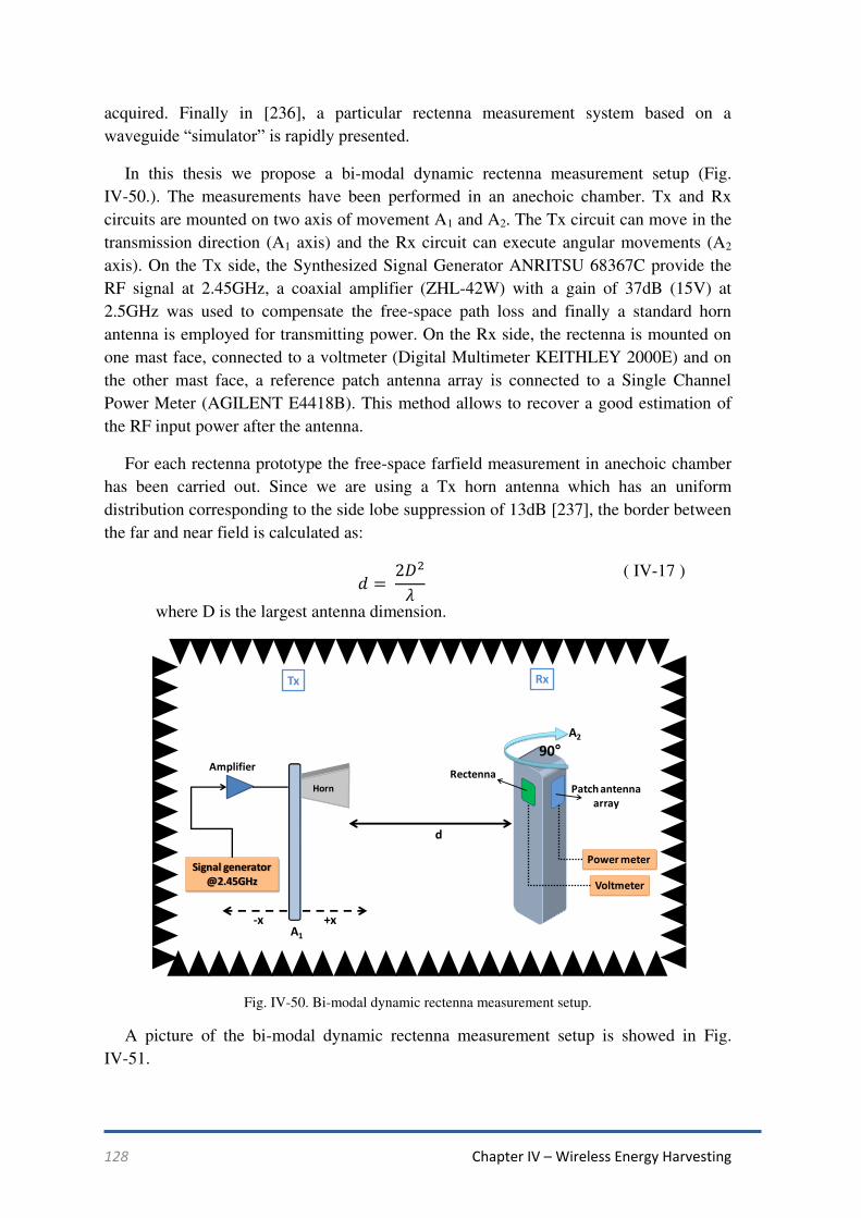
128 Chapter IV – Wireless Energy Harvesting
acquired. Finally in [236], a particular rectenna measurement system based on a
waveguide “simulator” is rapidly presented.
In this thesis we propose a bi-modal dynamic rectenna measurement setup (Fig.
IV-50.). The measurements have been performed in an anechoic chamber. Tx and Rx
circuits are mounted on two axis of movement A1 and A2. The Tx circuit can move in the
transmission direction (A1 axis) and the Rx circuit can execute angular movements (A2
axis). On the Tx side, the Synthesized Signal Generator ANRITSU 68367C provide the
RF signal at 2.45GHz, a coaxial amplifier (ZHL-42W) with a gain of 37dB (15V) at
2.5GHz was used to compensate the free-space path loss and finally a standard horn
antenna is employed for transmitting power. On the Rx side, the rectenna is mounted on
one mast face, connected to a voltmeter (Digital Multimeter KEITHLEY 2000E) and on
the other mast face, a reference patch antenna array is connected to a Single Channel
Power Meter (AGILENT E4418B). This method allows to recover a good estimation of
the RF input power after the antenna.
For each rectenna prototype the free-space farfield measurement in anechoic chamber
has been carried out. Since we are using a Tx horn antenna which has an uniform
distribution corresponding to the side lobe suppression of 13dB [237], the border between
the far and near field is calculated as:
( IV-17 )
where D is the largest antenna dimension.
Fig. IV-50. Bi-modal dynamic rectenna measurement setup.
A picture of the bi-modal dynamic rectenna measurement setup is showed in Fig.
IV-51.
90
Signal generator
@2.45GHz
Amplifier
d
Rectenna
Patch antenna
array
Voltmeter
Power meter
Horn
-x
Tx Rx
+xA1
A2

Chapter IV – Wireless Energy Harvesting 129
Fig. IV-51. Picture of the bi-modal dynamic rectenna measurement setup.
IV.5.2.1. Rectenna prototype #1
The first rectenna is composed of the rectifier #4 described previously and the antenna
patch array with high-orders harmonic-rejection that was described in Chapter III
(III.3.4.1). Both circuits have been developed separately with a 50Ω input matching
impedance. Then they have been assembled to create the rectenna #1. The rectenna
prototype #1 layout is presented in Fig. IV-52 without the lumped elements.
Fig. IV-52. Rectenna prototype #1 layout.
In Fig. IV-52 we can identify the patch antenna array then two high-orders harmonic-
rejection stubs, one for the 4.λGHz and the second for 7.35GHz. The 50Ω interface connects the antenna to the rectifier. An improvement on the voltage output measurement
process has been implemented in the rectenna design; from the DC load terminals a high-
impedance line brings the DC voltage through a RF-block inductor and consequently the
probe voltage can acquire the output voltage. Therefore, the measurements results are less
sensible to the measurement probe effect.
The rectenna #1 has been fabricated and characterized.
Schottky diode
DC load
RF-block

130 Chapter IV – Wireless Energy Harvesting
Fig. IV-53. Rectenna prototype #1 picture.
Based on the measurement setup presented in Fig. IV-50, the output voltage and RF-
DC conversion efficiency of the rectenna #1 have been acquired for a RF input power
from -40dBm to 0dBm. Fig. IV-54 shows the rectenna measurements results when the Tx
and Rx circuits respect the farfield constraint (128cm).
A high-RF-DC conversion efficiency of 35% for -15dBm input power is observed.
When the input power is decreased to a very-low input power of -30dBm, the rectenna
still provides 8% of conversion efficiency. Regarding the output voltage, 0.7V, this can
be achieved for a -3dBm RF input power.
(a) (b)
Fig. IV-54. Farfield rectenna #1 measurement results as a function of the RF incident power: a) RF-DC conversion efficiency, (b) output voltage.
As highlighted in Chapter I, to smooth the comparison of different sources of energy
harvesting, the conversion efficiency should be normalized with respect to the available
power density. Fig. IV-55 shows the RF-DC efficiency and the output voltage as a
function of the RF power density. As presented in (IV-1), the power density can be
calculated from the measured RF input power divided by the effective aperture area of the
antenna. The patch antenna array used in these rectennas has a measured gain of 6.7dB
(III.3.4). Thus the power density can be estimated and the measurements results of the
-40 -35 -30 -25 -20 -15 -10 -5 00
5
10
15
20
25
30
35
40
45
50
Eff
(%)
Pin
(dBm)-40 -35 -30 -25 -20 -15 -10 -5 00
0.1
0.2
0.3
0.4
0.5
0.6
0.7
0.8
0.9
1
VD
C(V
)
Pin
(dBm)

Chapter IV – Wireless Energy Harvesting 131
RF-DC efficiency and output voltage are presented in Fig. IV-55. From a low power
density of 1µW/cm2, the rectenna #1 already provides 40% of RF-DC efficiency.
(a) (b)
Fig. IV-55. Farfield rectenna #1 measurement results as a function of the RF power density: a) RF-DC conversion efficiency, (b) output voltage.
IV.5.2.2. Rectenna prototype #2
For the development of the second rectenna, the rectifier was co-designed with the
patch antenna array. The aim of this co-design is to reduce the rectenna size. First of all,
the patch antenna array has been designed (Chapter III.3.4.2), and then, from simulation
results, the antenna input complex impedance was acquired. The rectifier has been
designed based on the method described previously for the case study 2, i.e., after the
Schottky diode a microstrip line length should be carefully designed in order to present a
90° phase delay for the f0 and an open-circuit behavior for the 2f0.
Fig. IV-56. Rectenna prototype #2 layout.
The microstrip line dimensions are: length L=9mm and width W=2 mm. The design of
the impedance matching network at the circuit input relies on two criteria: to match the
0 2 4 6 8 10 12 14 160
5
10
15
20
25
30
35
40
45
50
Eff
(%)
Power Density (µW/cm2)
0 2 4 6 8 10 12 14 160
0.1
0.2
0.3
0.4
0.5
0.6
0.7
0.8
0.9
1
VD
C(V
)
Power Density (µW/cm2)
Schottky diode
DC load
RF-block

132 Chapter IV – Wireless Energy Harvesting
antenna impedance at 2.45GHz and to eliminate the second and third high-order
harmonics. The rectenna #2 layout is presented in Fig. IV-56.
The rectenna #2 has been fabricated (Fig. IV-57) and characterized.
Fig. IV-57. Rectenna prototype #2 picture.
Based on the measurement setup presented in Fig. IV-50, the output voltage and RF-
DC conversion efficiency of the rectenna #1 were acquired for a RF input power from -
40dBm to 0dBm. Fig. IV-58 shows the rectenna measurements results when the Tx and
Rx circuits respect the farfield constraint. A high-RF-DC conversion efficiency of 33%
for -15dBm input power was observed. When the input power is decreased to a very-low
input power of -30dBm, the rectenna still provides 7% of conversion efficiency.
Regarding the output voltage, 1 V can be achieved for a 0 dBm RF input power.
(a) (b)
Fig. IV-58. Farfield rectenna #2measurement results as a function of the RF incident power: a) RF-DC conversion efficiency, (b) output voltage.
Fig. IV-59 shows the RF-DC conversion and output voltage measurements as a
function of the RF power density.
-40 -35 -30 -25 -20 -15 -10 -5 00
5
10
15
20
25
30
35
40
45
50
Eff
(%)
Pin
(dBm)-40 -35 -30 -25 -20 -15 -10 -5 00
0.1
0.2
0.3
0.4
0.5
0.6
0.7
0.8
0.9
1
VD
C(V
)
Pin
(dBm)

Chapter IV – Wireless Energy Harvesting 133
(a) (b)
Fig. IV-59. Farfield rectenna #2 measurement results as a function of the RF power density: a) RF-DC conversion efficiency, (b) output voltage.
IV.6. Conclusion, comparison with the state of the art and perspectives for
future work
In this chapter, we demonstrated a new approach for the design of highly efficient
rectifiers and rectennas for very-low-power applications. An optimum RF-DC load is
required in order to achieve high RF-DC conversion efficiency. A careful numerical
assessment is important with the aim of predicting a correct Schottky diode model with its
parasites, as well as the right models for lumped elements. A thorough and accurate
rectenna free-space characterization is mandatory, since small errors in the measurements
of the received-power/available-power-density or output voltage have a large effect on
the RF-DC conversion efficiency results.
In order to highlight the importance of the RF-DC load, an original method to design a
rectifier with the help of Computer Controlled Microwave Tuner (CCMT) was carried
out. This method consists in providing different values of the load impedance (capacitive
or inductive) at the output terminal of a Schottky diode, preserving the RF-DC conversion
efficiency. From the Microwave tuner measurements, a group of optimum load
impedances has been identified where the RF-DC conversion efficiency was maximal.
Then two possible case studies were put in evidence in order to understand the link
between high RF-DC efficiency and these impedance values. Several rectifiers’ prototypes have been designed applying the two case studies (subtopic: IV.5.1). Finally,
from the rectifiers measurements results, the case study 2 appears as the best assumption,
i.e., to improve the RF-DC conversion efficiency, the load should present an open-circuit
for the second harmonic (2f0) and a 90° phase delay for the fundamental signal (f0). The
best rectifier prototype (#4) has been chosen for the rectenna design. Two rectennas have
been designed and prototyped (subtopic: IV.5.2). An original free-space rectenna
characterization was accomplished in an anechoic chamber, where with the help of two
axis of movement the RF received power and output voltage could be measured for the
same power density. Further, farfield measurements could be performed due to the second
movement axis (boresight direction).
0 2 4 6 8 10 12 14 16 180
5
10
15
20
25
30
35
40
45
50E
ff(%
)
Power Density (µW/cm2)
0 2 4 6 8 10 12 14 16 180
0.1
0.2
0.3
0.4
0.5
0.6
0.7
0.8
0.9
1
VD
C(V
)
Power Density (µW/cm2)

134 Chapter IV – Wireless Energy Harvesting
At 2.45GHz, included in the industrial-scientific-medical (ISM) band, the expected
available power density is around µW/cm2 level. In [238] the available power density in
an indoor WLAN scenario has been presented, following the recommendations of the
European Conference on Postal and Telecommunications Administrations (CEPT) [239];
10µW/m2 power density has been detected from 7m of the WLAN router. In [240], a
power density of 125µW/cm2 (ISM band) was enough to power a wireless sensor, which
consumes 1µA at 2.5V. Recently, E. Falkenstein et al. [56] presented a rectenna which
has 44% RF-DC conversion efficiency at 2.45GHz for a 25µW/cm2 power density.
According to them, the RF-DC efficiency reported in their paper is the highest
demonstrated for these power levels. However, we have found two other papers that have
reported high-efficiency RF-DC for lower power densities [57] and [62].
Table IV.1 gives an overview of rectennas and rectifiers, including the results obtained
in this thesis. It is important to note that due to the multiple efficiency definitions and
different prototype technologies existent in the literature, it is quite difficult to compare
the efficiency numbers directly. As described in Chapter I, another critical point is the
normalization of the RF-DC efficiency as a function of received power or power density.
Nevertheless, the results listed in this table have been extracted exactly as they are
reported in the literature.
TABLE IV.1 OVERVIEW OF RECTENNAS AND RECTIFIERS STATE OF THE ART
Reference ηRF-DC Incident RF power/
power density Frequency
(GHz) Single/Multi
band Substrate
[55] - 2013 10% -13dBm, 0.05mW 2.45 Multiband RF-60A-Taconic
[56] - 2012 44% 25µW/cm2 2.45 Single-band ROGERS
4350B
[57] - 2012 50% -17.2dBm (0.22µW/cm2) 2.45 Single-band RT/Duroid
6002
[58] - 2011 63% 0.525 mW/cm2 2.45 Single-band Duroid 5880
[59] - 2010 16% -20dBm 2.45 Single-band Arlon A25N
[60] - 2010 52% +10 dBm, 10mW
(150µW/cm2) 2.45 Single-band -
[61] - 2010 25% 0 dBm, 1 mW 2.45 Single-band Arlon 25N
[62] - 2010 34% -10 dBm, 100µW (17
µW/cm2) 2.45 Single-band Arlon
AD320 [63] - 2006 45% +10dBm, 10mW 2.45 Single-band FR4
[64] - 2005 40% +20 dBm, 100mW 2.45 Single-band FR4
[65]- 2002 84% +19.5dBm, 89.84mW 2.45 Dual-band Duroid587
0
[66] - 2000 62% 0dBm, 1mW 2.45 Single-band RT /Duroid
5870
[67] - 1991 50% +13dBm, 20mW 2.45 Single-band -
Rectifier #1 70% 0dBm, 1mW 2.45 Single-band ROGERS
4003
Rectifier #4 36% -10dBm, 100µW 2.45 Single-band ROGERS

Chapter IV – Wireless Energy Harvesting 135
4003
Rectifier #5 18% -15dBm, 32µW 2.45 Single-band ROGERS
4003
Rectenna #1 29% -19dBm, 10µW (0.15µW/cm2) 2.45 Single-band ROGERS
4003
Rectenna #2 41% -9dBm, 31µW (0.33µW/cm2) 2.45 Single-band ROGERS
4003
For a more clear State-of-the-Art comparison and considering that some papers report
the RF-DC efficiency results as a function of the RF incident power (dBm) and others as
a function of RF power density (µW/cm2), we have plotted two graphs for the RF-DC
conversion efficiency: Fig. IV-60 (as a function of the RF incident power) and Fig. IV-61
(as a function of the RF power density). It is important to notice that the results (Table
IV.1) which have an incident power upper than 0dBm or a power density upper than
30µW/cm2, are not considered in our comparison, since we focus on the Wireless Energy
Harvesting applications (very-low-power available).
Fig. IV-60. Rectennas state-of-the-Art at 2.45 GHZ based on the RF-DC conversion efficiency as a function of incident RF power.
-40 -35 -30 -25 -20 -15 -10 -5 00
5
10
15
20
25
30
35
40
45
50
55
Eff
(%)
Pin
(dBm)
Rectennas developed in this thesis compared with the State-Of-The-Art(2014)
[55]
[57]
[59]
[61]
[62]
Rectenna#1
Rectenna#2
State-of-the-Art (<2014)

136 Chapter IV – Wireless Energy Harvesting
Fig. IV-61. Rectennas state-of-the-Art at 2.45 GHZ based on the RF-DC conversion efficiency as a function of RF power density.
Since high-efficiency rectenna has emerged nowadays as an urgent and challengeable
issue for low-power RF energy harvesting applications, from state-of-the-art comparison
presented in Fig. IV-60 and Fig. IV-61, we can considerer the study reported in this thesis
as a pointed attempt in this direction.
Future work:
The high-efficient rectifiers and rectennas designed in this thesis, can be employed
directly in power wireless sensor, where there is no battery needed, i.e., for instant energy
utilization and without any need of an embedded power management circuitry.
Nevertheless, due to the rectifier’s high efficiency values, it should be interesting to integrate this rectifier in an autonomous wireless sensor powered by RF energy, as
described in Fig. IV-1. From (IV-7) we demonstrated that the lowest conversion
efficiency in a such autonomous sensor is the RF-DC conversion. Thus, we expect that
with the results acquired in this thesis we could to improve the State-of-the-Art of the
complete low-power energy harvesting systems (rectenna + super-capacitor storage +
load).
A second perspective idea comes from the fact that during the rectennas
characterization in the anechoic chamber, farfield measurements, but also preliminary
nearfield measurements have been performed, since we were interested to uncover the
behavior of the rectenna when closer to the RF source. Since nearfield environment needs
a special attention on the formulation and analysis, we are taking these first results
carefully. Moreover, the different field regions around an antenna are described in
Chapter III (III.2.3)
0 5 10 15 20 25 300
5
10
15
20
25
30
35
40
45
50
55E
ff(%
)
Power Density (µW/cm2)
Rectennas developed in this thesis compared with the State-Of-The-Art(2014)
[56]
[57]
[62]
Rectenna#1
Rectenna#2
State-of-the-Art (<2014)

Chapter IV – Wireless Energy Harvesting 137
For both rectennas (#1 and #2), measurements in a nearfield situation were carried out
following the measurement setup presented in Fig. IV-50, and for each output voltage
value acquired, the received power was effectively measured by means of the reference
antenna. The Tx and Rx antennas were separated by 74cm.
Fig. IV-62 shows the rectenna #1 nearfield measurement results as a function of the
power density.
(a) (b)
Fig. IV-62. Nearfield rectenna #1 measurement results as a function of the RF power density: a) RF-DC conversion efficiency, (b) output voltage.
Fig. IV-63 shows the rectenna #2 nearfield measurements results as a function of the
power density.
(a) (b)
Fig. IV-63. Nearfield rectenna #2 measurement results as a function of the RF power density: a) RF-DC conversion efficiency, (b) output voltage.
From the rectenna measurements results, an important difference is noticed between
the near and far field measurements. Thus, we expect to continue in a future work with
the near-field analysis in the purpose of understanding the preliminary results observed.
0 5 10 15 20 25 300
10
20
30
40
50
60
70
80
90
Eff
(%)
Power Density (µW/cm2)
0 5 10 15 20 25 300
0.2
0.4
0.6
0.8
1
1.2
1.4
1.6
1.8
VD
C(V
)
Power Density (µW/cm2)
0 5 10 15 20 25 300
10
20
30
40
50
60
70
80
Eff
(%)
Power Density (µW/cm2)
0 5 10 15 20 25 300
0.2
0.4
0.6
0.8
1
1.2
1.4
1.6
1.8
VD
C(V
)
Power Density (µW/cm2)

138 Chapter IV – Wireless Energy Harvesting
However, in the literature a recent paper seems started to observe the same phenomena in
a nearfield zone [241].

Chapter V - Conclusion 139
Chapter V - Conclusion and perspectives
V.1. Summary of results
DSRC e-toll collection application is a complex and complete system, in which each
block should be developed respecting the DSRC standards and practical criteria.
Therefore, in this thesis, important DSRC blocks have been developed in order to
guarantee the best performance for the whole system.
Regarding the DSRC OBU, since DSRC e-toll system is a broad commercial
application, finding references and information about these products is not trivial. Thus,
to start our own OBU design, we needed to characterize different DSRC OBU available
on the market in order to have access to their electric power consumption. From the
measurement results, we observed that the classical DSRC OBUs still demand an
important amount of energy per day (4J), this implying a battery life of 4-6 years. Thus,
designing a completely autonomous DSRC transponder is not feasible, since the amount
of energy required is still high. Nevertheless, reducing the transponder electric power
consumption, as a solution to at least double the battery life, could be a good start point to
improve environment protection and customer satisfaction. We have proposed a new
DSRC transponder with an original statechart that considerably reduces the power
consumption. First of all, we have proceeded with the DSRC chip characterization, an
evaluation board has been engineered to assist the characterization measurements. We
implemented a deep-sleep mode based on a vibration sensor, a mobile evaluation board
supplied by a USB port has been engineered. In-situ tests have been performed. Due to
this supplementary operational mode, the electric power consumption has been
considerably reduced. The new DSRC transponder proposed in this thesis consumes 13x
less energy compared to the classical DSRC transponder available on the market,
regarding the energy consumption per day.
Once the electric power consumption of the new DSRC transponder has been
considerably reduced, the feasibility of recharging the battery of the OBU by means of
Wireless Energy Harvesting (WEH) has been analyzed. From a friendly environmental
and economic point of view, finding a solution for the battery replacement and its discard
is an important question nowadays. The amount of RF energy that could be harvested by
the OBU for the two DSRC e-toll cases (Free-Flow and Stop&Go) was estimated through
the RF link budget. Only for the Stop&Go configuration (stop time>2s), the RF energy
harvesting could become attractive to power the transponder. A recovered energy of 10µJ
could be achieved if the driver spends 2s in the RSE antenna field. Nevertheless, even
with the transponder power consumption proposed in this thesis (314mJ), the recovered
energy by means of DSRC Wireless Energy Harvesting would not be enough. Based on
this analysis, we have decided to explore the Wireless Energy Harvesting for other
frequency than the DSRC 5.8GHz frequency. We have chosen the 2.45 GHz as it is part

140 Chapter V - Conclusion
of the ISM band, many authors described their research on WEH for this frequency and
we have been able to compare our results with the state of art.
We have demonstrated a new approach for the design of highly efficient rectifiers and
rectennas for very-low-power applications. An optimum RF-DC load is required in order
to achieve high RF-DC conversion efficiency. A cautious numerical assessment is
important in the aim of predicting a correct Schottky diode model with its parasites, as
well as the right models for lumped elements. A thorough and accurate rectenna free-
space characterization is mandatory, since small errors in the measurements of the
received-power/available-power-density or output voltage have a large effect on the RF-
DC conversion efficiency results. With the aim of demonstrating how to achieve high
conversion efficiencies values, an original measurement setup was implemented based on
a Computer Controlled Microwave Tuner (CCMT), in which different values of the load
impedance (capacitive or inductive) have been presented at the output terminal of a
Schottky diode. Several rectifiers and rectennas have been designed, fabricated and
characterized in order to validate our method. Regarding the rectenna measurement setup,
we implemented an appropriate method, since to calculate the RF-DC conversion
efficiency, we need to acquire for the same energy density, the RF power at the rectifier
input and the output voltage. Finally, the results obtained in this thesis are in the forefront
of the State-of-the-Art (45% of RF-DC conversion efficiency) in WEH for very low
available power density (5µW/cm2).
In the special context of this thesis, at the same time Multitoll Company requires
practical and reliable antenna solutions for their applications, but also we aim to further
the state of the art through different ideas. We provided therefore, several antennas for
DSRC and WEH. The first one is the OBU antenna, a 5.8GHz patch antenna has been
designed and good results have been achieved (gain value of 8dB and S11 value of -18dB).
This antenna is integrated with the OBU device produced by Multitoll recently. The
second antenna we have studied, fabricated and characterized is the 1x3 patch array with
superstrate layers. We have successfully designed this antenna with a high gain (13.8dB)
and a small “visible surface” (condition requested by Multitoll). Nevertheless, an issue
has been detected in the reproducibility of the antenna prototypes due the VIAs
connections. Given this, we have decided to use a different feeding method for the next
antennas, which should be easy to fabricate in large-scale and presents a lower margin of
error between the different fabricated prototypes. The third DSRC antenna developed is
based on a patch antenna array with 8 elements and has a special sequential rotation
feeding that allowed us to significantly improve the antenna polarization (AR=-1.5dB
with radome). Once the antenna PCB design has been realized and since this antenna
should be inserted in a real box with DSRC reader, we have studied and optimized the
antenna considering the radome and metallic plate (for RF/electronic separation). As
described before, these antennas are part of a complete and complex system, and two
different in-situ test scenarios have been carried out in order to evaluate the practical
antenna performance. Finally, WEH devices need also antennas, since rectennas are a
combination of rectifier and antenna, then two rectennas have been designed, fabricated

Chapter V - Conclusion 141
and tested based on microstrip patch antenna array with high-order harmonics rejection.
The first rectenna has been directly assembled with the rectifier, however, for the second
rectenna a co-design process has been carried out in order to optimize the occupied PCB
area.
In this thesis new results on Wireless Energy Harvesting domain have been
successfully reported, but also many research technologies have been transferred and
adapted to an industrial application of e-toll under the DSRC protocol. All these work
results responded to the company requests.
To resume, the main contributions of this thesis are:
To ensure a correct operation of the DSRC e-toll system, each part of the
system should be analyzed, designed and tested as a part of a complete and
complex system. Therefore, in this thesis, important DSRC blocks have been
developed in order to guarantee the best performances for the whole system:
o The antennas, both OBU and RSE have been studied, designed and
tested in a real DSRC e-toll in-situ scenario.
o The OBU front-end design and implementation have been carried out.
o A new DSRC OBU deep-sleep mode has been implemented by means
of an original wake-up vibration sensor, that allowed a considerable
power consumption reduction.
o The DSRC V2I link budget modeling for e-toll systems has been
successfully developed. Several parameters have been taken into
account on the link budget modeling, e.g., car’s windshield attenuation, RSE antenna specifications and vehicle speed. In the literature, to the
best of our knowledge, only quite few papers explored this topic.
The possibility to recharge electronic devices remotely by means of microwave
energy is quite attractive, therefore in this thesis, the Wireless Energy
Harvesting has been studied:
o Our work demonstrates that high-efficient rectifier/rectenna for low
input power is feasible.
o An important effort has been made in order to elucidate in detail how to
achieve high efficiencies levels with a single diode and a simple load.
o In the aim of demonstrating how to achieve high conversion
efficiencies values, an original measurement setup has been
implemented based on a Computer Controlled Microwave Tuner
(CCMT). Different values of the load impedance (capacitive or
inductive) were presented at the output terminal of a Schottky diode.

142 Chapter V - Conclusion
o Several rectifiers and rectennas have been designed, fabricated and
characterized in order to validate our method.
o Regarding the rectenna measurement setup, we have implemented an
appropriate method, since to calculate the RF-DC conversion
efficiency, we need to acquire for the same energy density, the RF
power on the rectifier input and the output voltage.
o A different approach has been provided regarding the difference
between Wireless Power Transfer (WPT) and Wireless Energy
Harvesting (WEH). Moreover, we have reminded the difficulty to
compare the different results in Energy Harvesting literature due to the
lack of standardization on the unit of available power density.
o Finally, the results obtained in this thesis are in the forefront of the
State-of-the-Art of Wireless Energy Harvesting for very low available
power density.
V.2. Perspectives
DSRC protocol needs complex and reliable RF transactions in order to ensure the
payment, as well as the protection of the client’s personal information. In this thesis, the
high electric power consumption of DSRC protocol has been highlighted. Industrial
approaches exist for reducing the electric power consumption of the DSRC protocol (e.g.,
DSRC OBU completely reflexive, does not need local oscillators to generate the RF
wave). However, there is still a lot of work to do in this field. We could imagine the
timeline presented in Fig. V-1, where the energy consumption of the DSRC OBU is
compared to the energy that could be harvested in the DSRC e-toll scenario.
Fig. V-1. Timeline of energy requested by the DSRC OBU compared to the amount of energy that could be harvester by means of WEH.
In this thesis, the points A and B have been well established, a new low-power DSRC
transponder have been proposed, and as well, the DSRC RF link budget has been carried
out, demonstrating the amount of energy that could be harvested in the DSRC band. An
5µ
4
0.3
C
B
A
D

Chapter V - Conclusion 143
important observation is that, as discussed in Chapter I, nowadays, the tendency in
advances of integrated low-power circuit technology is the reduction of the required
energy by the electronic. Thus, WEH arises in an appropriate time, where the key is to
find the point-of-compromise between requested energy and energy harvested from
ambient sources (point C in Fig. V-1). However, we could also dream on that one day the
point D could be reached by DSRC applications, where a completely autonomous DSRC
OBU will be available on the market.

144 References
References [1] K. Sangani, “The sun in your pocket,” IET Engineering and Technology magazine, pp. 36-38, Aug.
2007. [2] S. Roundy, P. Wright, and J.M. Rabaey, “Energy scavenging for wireless sensor networks with special
focus on vibrations,” 1st ed. London: Kluwer Academic Publishers, 2004. [3] T. Markvart and L. Castañer, “Practical Handbook of Photovoltaics: Fundamentals and Applications”.
2003. [4] J. P. Thomas, M. A. Qidwai, and J. C. Kellogg, "Energy scavenging for small-scale unmanned
systems," Journal of Power Sources, vol. 159, pp. 1494-1509, 2006. [5] A. Reinders, "Options for Photovoltaic Solar Energy Systems in Portable Products, " TMCE, 2002. [6] M. Veefkind and S. F. J. Flipsen, “Gathering data on the energy to be harvested with portable
consumer products, method and equipment," in Proceedings of the ISES EuroSun Congress, 2004. [7] M. Veefkind, “Industrial design and PV-power, challenges and barrieres," in Proceedings of the ISES
Solar World Congress, 2003. [8] ATA LABS. [Online] Available: http://atlalabs.com/ [9] Logitech wireless solar keyboard K750. [Online] Available: http://www.logitech.fr [10] CASIO GW-2000B-1AER solar atomic aviation G-shock watch. [Online] Available:
www.casio.co.uk/products [11] J. Matiko, N. Grabham, S. Beeby and M. Tudor, “Review of the application of energy harvesting in
buildings,” Electronics and Computer Science, University of Southampton, UK., 2013. [12] International thermoelectric society. Thermoelectric power for automobiles arrives in Europe. [Online]
Available: http://www.its.org/node/5670 [13] V. Leonov, T. Torfs, P. Fiorini, and C. Van Hoof, “Thermoelectric Converters of Human Warmth for
Self-Powered Wireless Sensor Nodes," Sensors Journal, IEEE, vol. 7, no. 5, pp. 650-657, 2007. [14] M. Stordeur and I. Stark, “Low power thermoelectric generator – selfsuient energy supply for micro
systems," in Proceedings of the 16th International Conference on Thermoelectrics, pp. 575-577, 1997. [15] I. Stark and M. Stordeur, “new micro thermoelectric devices based on bismuth telluride-type thin
solid'," in Proceedings of the 18th International Conference on Thermoelectronics, pp. 465-472, 1999. [16] X. Lu and S-H. Yang, “Thermal energy harvesting for WSNs”, IEEE Int. Conf. on Systems, Man and
Cybernetics, pp 3045–52, Oct. 2010. [17] C. Knight, J. Davidson, and S. Behrens, "Energy Options for Wireless Sensor Nodes," Sensors, vol. 8,
pp. 8037-8066, 2008. [18] S. Beeby, M. Tudor and N. White, “Energy harvesting vibration sources for microsystems
applications,” Meas. Sci. Technol. 17 R175–95, 2006. [19] D. Zhu, M. Tudor and S. Beeby, “Strategies for increasing the operating frequency range of vibration
energy harvesters: a review,” Meas. Sci. Technol. 21 022001, 2010. [20] R. N. Torah, S. P. Beeby, M. J Tudor, T. O'Donnell, and S. Roy, “Development of a cantilever beam
generator employing vibration energy harvesting,” in 6th international workshop on micro and
nanotechnology for power generation and energy conversion applications (PowerMEMS 2006), Dec. 2006.
[21] M. Mizuno, and D. Chetwynd, “Investigation of a resonance microgenerator”, J. Micromech. Microeng., pp. 209-216, 2003.
[22] C.Shearwood, and R. Yates, “Development of an electromagnetic microgenerator,” Electron. Lett., pp. 1883-1884, 1997.
[23] H. Kulah, and K. Najafi, “An electromagnetic micro power generator for lowfrequency environmental vibrations,” 17th IEEE international conference on micro electro mechanical systems (MEMS ’04), pp. 237-240, Jan. 2004.
[24] R. Amirtharajah, and A. Chandrakasan, “Self-powered signal processing using vibration-based power generation,” IEEE J. Solid-State Circuit, pp. 687-695, 1998.
[25] P. D. Mitcheson, T. C. Green, E. M. Yeatman, and A. S. Holmes, “Architectures for vibration-driven micropower generators," J. of Microelec- tromechanical Systems, vol. 13, no. 3, Jun. 2004.
[26] S. Meninger, J. Mur-Miranda, R. Amirtharajah, A. P. Chandrasakan, and J. H. Lang, “Vibration to electric energy conversion," IEEE Trans. on VLSI, vol. 9, no. 1, Feb. 2001.
[27] S. Roundy, P. Wright, and J. Rabaey, “A study of low level vibrations as a power source for wireless sensor nodes," Computer Communications, vol. 26, no. 11, pp. 1131-1144, 2003.
[28] S. Roundy, B. P. Otis, Y.-H. Chee, J. M. Rabaey, and P. Wright, “A 1.9 GHz rf tansmit beacon using environmentally scavenged energy," in Proceedings of the ISPLED, 2003.

References 145
[29] S. Roundy, P. Wright, and K. Pister, “Micro-electrostatic vibration-to-electricity converters," in Proceedings of ASME International Mechanical Engineering Congress and Exposition IMECE2002, vol. 220, pp. 17-22, Nov. 2002.
[30] S. Roundy, E. Leland, J. Baker, E. Carleton, E. Reilly, E. Lai, B. Otis, J. Rabaey, P. Wright, and V. Sundararajan, “Improving power output for vibration-based energy scavengers," in IEEE Pervasive
Computing, vol. 4, no. 1, pp. 28-36, 2005. [31] S. Roundy, P. K. Wright, and J. M. Rabaey, “Energy scavenging for wire-less sensor networks with
special focus on vibrations,” Kluwer Academic Publishers, 2004. [32] H. Hu, H. Xue, and Y. Hu, “A spiral-shaped harvester with an improved harvesting element and an
adaptive storage circuit,” IEEE Transactions on Ultrasonics, Ferroelectrics and Frequency Control, vol. 54, no. 6, pp. 1177-1187, Jun. 2007.
[33] G. Ottman, H. Hofmann, A. Bhatt, and G. Lesieutre, “Adaptive piezoelectric energy harvesting circuit for wireless remote power supply,” IEEE Trans. on Power Electronics, vol. 17, no. 2, pp. 669-676, Sep. 2002.
[34] G. Ottman, H. Hofmann, and G. Lesieutre, “Optimized piezoelectric energy harvesting circuit using step-down converter in discontinuous conduction mode,” IEEE Trans. on Power Electronics, vol. 18, no. 2, pp. 696-703, Mar. 2003.
[35] W. Wu, Y. Chen, B. Lee, J. He, Y. Peng. “Tunable resonant frequency power harvesting devices”. Proc SPIE, 2006.
[36] C. B. Williams and R. B. Yates, "Analysis of a micro-electric generator for microsystems," Stockholm, Sweden, pp. 369-372, 1995.
[37] N. N. H. Ching, W. J. Li, P. H. W. Leong, Z. Wen, and H. Y. Wong, "A laser micromachined multi-modal resonating power transducer for wireless sensing systems," Munich, pp. 685-690, 2002.
[38] Hinchet R., Lee S., Ardila G., Montes L., Mouis M., Wang Z. L., "Performance Optimization of Vertical NW-Based Piezoelectric Nanogenerators", Advanced Functional Materials, Oct. 2013.
[39] R. Hinchet, S. Lee, G. Ardila, L. Montes, M. Mouis and Z-L. Wang , "Design and Guideline Rules for the Performance Improvement of Vertically Integrated Nanogenerator", Journal of Energy and Power
Engineering, Sept. 2013. [40] Ardila G., Hinchet R., Mouis M., Montes L., "Scaling prospects in mechanical energy harvesting with
piezo NWs", The European Physical Journal Applied Physics, Jul. 2013. [41] Nikola Tesla, "Apparatus for the Utilization of Radiant Energy," U.S. Patent No. 685,957, Nov. 5,
1901; and "A Method of Utilizing Radiant Energy," U.S. Patent No. 685-958, Nov. 5, 1901. [42] Experimental Airborne Microwave Supported Platform. Descriptive Note : Final rept. Jun 64 – Apr 65 [43] G. A. Landis, "Applications for Space Power by Laser Transmission," SPIE Optics, Electro-optics &
Laser Conference, Vol. 2121, 252–255, Jan. 1994. [44] W. C. Brown, “The history of power transmission by radio waves,” IEEE Trans. Microwave Theory
Tech., vol. MTT-32, pp. 1230–1242, Sept.1984. [45] G. Landis, M. Stavnes, S. Oleson and J. Bozek, "Space Transfer With Ground-Based Laser/Electric
Propulsion" (AIAA-92-3213) NASA Technical Memorandum TM-106060 (1992). [46] Powercast Corp.. (2012). Powercast Overview - RF Energy Harvesting and Wireless Power for Micro-
Power Applications. [Online]. Available: http:// www.powercastco.com/ [47] The economist Group Corp. (2007). When everything connects. [Online]. Available:
http://www.economist.com/node/9080024. [48] Y.-C. Cheng, Y. Chawathe, A. LaMarca, J. Krumm, “Accuracy characterization for metropolitan-scale
Wi-Fi localization”, Proc. Third Int. Conf. on Mobile Systems, pp. 233–245, Jan. 2005. [49] Nicolas Mokhoff. (2011, Juin 12). EE Times' 20 hot technologies for 2012. [Online]. Available:
http://www.eetimes.com/author.asp?section_id=36&piddl_msgorder=thrd&doc_id=1266037&page_number=2
[50] Rajiv Kumar. (2011, October). Top 50 Technologies Reshaping the World. [Online]. Available: http://www.growthconsulting.frost.com/web/images.nsf/0/A86A27D34190816465257937004BAA06/$File/GIL1011_TECHVISION%202020.htm
[51] Dr Peter Harrop and Raghu Das. (2012, October). Energy Harvesting and Storage for Electronic Devices 2012-2022: Forecasts, Technologies, Players. [Online]. Available: http://www.idtechex.com/research/reports/energy-harvesting-and-storage-for-electronic-devices-2012-2022-000316.asp?viewopt=desc
[52] U. Olgun, C.-C. Chen, and J. Volakis, “Design of an efficient ambient wifi energy harvesting system,” IET Microw. Antennas Propag. ,vol.6, no. 11, pp. 1200–1206, Aug. 2012.
[53] J. Masuch, M. Delgado-Restituto, D. Milosevic, P. Baltus, "Co-Integration of an RF Energy Harvester Into a 2.4 GHz Transceiver," Solid-State Circuits, IEEE Journal of , vol.48, no.7, pp.1565-1574, Jul. 2013.

146 References
[54] V. Marian, B. Allard, C. Vollaire, J. Verdier, "Strategy for Microwave Energy Harvesting From Ambient Field or a Feeding Source," Power electronics, IEEE Transactions on, vol.27, no.11, pp.4481-4491, Nov. 2012.
[55] D. Masotti, A. Costanzo, M. Del Prete, V. Rizzoli, "Genetic-based design of a tetra-band high-efficiency radio-frequency energy harvesting system," Microwaves, Antennas & Propagation, IET, vol.7, no.15, pp.1254-1263, Dec. 2013.
[56] Erez Falkenstein, Michael Roberg, Z. Popovic, "Low-Power Wireless Power Delivery," Microwave
Theory and Techniques, IEEE Transactions on , vol.60, no.7, pp.2277-2286, Jul. 2012 [57] Hucheng Sun; Yong-Xin Guo; Miao He; Zheng Zhong, "Design of a High-Efficiency 2.45-GHz
Rectenna for Low-Input-Power Energy Harvesting," Antennas and Wireless Propagation Letters,
IEEE, vol.11, no., pp.929-932, 2012. [58] Z. Harouni, L. Cirio, L. Osman, A. Gharsallah, O. Picon , "A Dual Circularly Polarized 2.45-GHz
Rectenna for Wireless Power Transmission," Antennas and Wireless Propagation Letters, IEEE , vol.10, no., pp.306-309, 2011.
[59] G. Andia Vera, A. Georgiadis, A. Collado, S. Via, "Design of a 2.45 GHz rectenna for electromagnetic (EM) energy scavenging," Radio and Wireless Symposium (RWS), 2010 IEEE , vol., no., pp.61-64, Jan. 2010.
[60] H. Takhedmit, B. Merabet, L. Cirio, B. Allard, F. Costa, C. Vollaire and O. Picon, “A 2.45-GHz low cost and efficient rectenna,” in Proc. 4th Eur. Antennas Propag. Conf., pp. 1–5, 2010
[61] H. Takhedmit, B. Merabet, L. Cirio, B. Allard, F. Costa, C. Vollaire, O. Picon, "A 2.45-GHz dual-diode RF-to-dc rectifier for rectenna applications," Microwave Conference (EuMC), 2010 European , vol., no., pp.37-40, Sept. 2010
[62] F. A. S. Riviere, A. Douyere, and J.-D. Lan Sun Luk, “A compact rectenna device at low power level,” Progr. Electromagn. Res. C, vol. 16, pp. 137–146, 2010.
[63] J. Zbitou, M. Latrach, and S. Toutain, “Hybrid rectenna and monolithic integrated zero-biasmicrowave rectifier,” IEEE Trans. Microw. Theory Tech., vol. 54, no. 1, pp. 147–152, Jan. 2006.
[64] J. Akkermans, M. van Beurden, G. Doodeman, and H. Visser, “Analytical models for low-power rectenna design,” IEEE Antennas Wireless Propag. Lett., vol. 4, pp. 187–190, 2005.
[65] Young-Ho Suh, Kai Chang, "A high-efficiency dual-frequency rectenna for 2.45- and 5.8-GHz wireless power transmission," Microwave Theory and Techniques, IEEE Transactions on, vol.50, no.7, pp.1784-1789, Jul. 2002.
[66] J. Heikkinen, P. Salonen, M. Kivikoski, "Planar rectennas for 2.45 GHz wireless power transfer," Radio and Wireless Conference, 2000, vol., no., pp.63-66, 2000.
[67] W. Brown, “An experimental low power density rectenna,” in IEEE MTT-S Int. Microw. Symp. Dig., vol. 1, pp. 197–200, Jul. 1991.
[68] EE Times (2009, November 11).Nokia working on energy-harvesting handset. Mag. [Online]. Available: http://www.eetimes.com/document.asp?doc_id=1253967C.
[69] Cseh, “Architecture of the Dedicated Short-Range Communications (DSRC) protocol”, Vehicular
Technology conference, VTC 98 48th IEEE, vol. 3 pp 2095-2099, 1998. [70] Kelly, Frank (2006): Road Pricing: Addressing congestion, pollution and the financing of Britain’s
road. Published in “Ingenia” by The Royal Academy of Engineering, volume 39, p. 36-42. [71] Dedicated Short-Range Communication (DSRC) - Physical CEN Standard EN 12253, 2004. [72] Dedicated Short-Range Communication (DSRC) - Data link layer: Medium Access and Logical Link
Control, CEN Standard EN 12795, 2002. [73] Dedicated Short Range Communication (DSRC) - DSRC application layer, CEN Standard EN 12834,
2003. [74] DSRC profiles for RTTT applications, CEN Standard EN 13372, 2004. [75] Interface for EFC – Electronic Fee Collection, CEN, ISO, and ETSI Standard EN ISO/ETSI 14906,
2004. [76] B. R. Franciscatto, T.-P. Vuong, T. Trang, C. Defay, "Microstrip-fed quasi-Yagi antenna array for a
different DSRC system," Antenna Technology and Applied Electromagnetics (ANTEM), 2012 15th
International Symposium on, vol., no., pp.1-5, Jun. 2012. [77] Kenney and John B., “Dedicated Short-Range Communications (DSRC) Standards in the United
States,” in Proceedings of the IEEE, Vol. 99, Issue: 7, pp. 1162–1182, Jul. 2011. [78] D. Tian, H. Luo, J. Zhou, H. Xia, "A Self-Adaptive V2V Communication System with DSRC," Green
Computing and Communications (GreenCom), 2013 IEEE and Internet of Things (iThings/CPSCom), IEEE International Conference on and IEEE Cyber, Physical and Social Computing , vol., no., pp.1528-1532, Aug. 2013.

References 147
[79] R. Sabouni, R. Hafez, "Performance of DSRC for V2V communications in urban and highway environments," 25th IEEE Canadian Conference Electrical & Computer Engineering (CCECE), vol., no., pp.1-5, Apr. 2012.
[80] K. Hong, J. Kenney, V. Rai, K. Laberteaux, "Evaluation of Multi-Channel Schemes for Vehicular Safety Communications," IEEE Vehicular Technology Conference (VTC 2010-Spring), vol., no., pp.1-5, May 2010.
[81] S. Chang, J. Jung, J. Cha, S. Lee, "Implementation of DSRC Mobile MAC for VANET," Advanced
Communication Technology (ICACT), 2011 13th International Conference on, vol., no., pp.1502-1505, Feb. 2011.
[82] V. Kukshya, H. Krishnan, "Experimental Measurements and Modeling for Vehicle-to-Vehicle Dedicated Short Range Communication (DSRC) Wireless Channels," Vehicular Technology
Conference, 2006. VTC-2006 Fall. 2006 IEEE 64th, vol., no., pp.1-5, Sept. 2006. [83] J. Fernandez, K. Borries, L. Cheng, B. Kumar, D. Stancil, F. Bai, "Performance of the 802.11p
Physical Layer in Vehicle-to-Vehicle Environments," Vehicular Technology, IEEE Transactions on , vol.61, no.1, pp.3-14, Jan. 2012.
[84] X. Ma, X. Chen, "Delay and Broadcast Reception Rates of Highway Safety Applications in Vehicular Ad Hoc Networks," 2007 Mobile Networking for Vehicular Environments , vol., no., pp.85-90, May 2007.
[85] S. Strin, M. Kang, J. Jin, S. Kim, H. Kim, S. Moh, "Vehicle-to-Vehicle emergency message dissemination through the WiBro network," Networked Computing (INC), 2010 6th International
Conference on, vol., no., pp.1-6, May 2010. [86] S. Biswas, R. Tatchikou, and F. Dion, “Vehicle-to-vehicle wireless communication protocols for
enhancing highway traffic safety,” IEEE Communications Magazine, vol. 44, pp. 74-82, Jan. 2006. [87] Fan Bai, H. Krishnan, "Reliability Analysis of DSRC Wireless Communication for Vehicle Safety
Applications," Intelligent Transportation Systems Conference, Page(s): 355-362, 2006. [88] Xianbo Chen, H.Refai, Xiaomin Ma, "A Quantitative Approach to Evaluate DSRC Highway Inter-
Vehicle Safety Communication," Global Telecommunications Conference, 2007. GLOBECOM '07. Page(s):151–155. Nov. 2007.
[89] L. Cheng, B. E. Henty, D. D. Stancil, F. Bai, P. Mudalige, “Mobile Vehicle-to-Vehicle Narrow-Band Channel Measurement and Characterization of the 5.9 GHz Dedicated Short Range Communication (DSRC) Frequency Band”, IEEE Journal on Selected Areas in Communications, Vol. 25, pp. 1501–1516, Oct. 2007.
[90] A. G. Emslie, R. L. Lagace, and P. F. Strong, “Theory of the propagation of UHF radio waves in coal mine tunnels,” IEEE Trans. Antennas Propag., vol. AP-23, pp. 192-205, Mar. 1975.
[91] Y. Yamaguchi, T. Abe, T. Sekiguchi, and J. Chiba, “Attenuation constants of UHF radio waves in arched tunnels,” IEEE Trans. Microw. Theory Tech., vol. MTT-33, no. 8, pp. 714-718, Aug. 1985.
[92] K. Fujimori and H. Arai, “Propagation characteristics in tunnels including base station antenna,” Electron. and Commun. in Japan (Part I: Commun.), vol. 84, iss. 4, pp. 1-10, April 2001.
[93] K. Uchida, H. Nose, H. Maeda, and T. Matsunaga, “Theoretical and experimental study of propagation in 3D tunnels,” IEICE Trans. Commun., vol. E87-B, no. 10, pp. 3044-3049, Oct. 2004.
[94] D. G. Dudley, and S. F. Mahmoud, “Linear source in a circular tunnel,” IEEE Trans. Antennas
Propag., vol. 54, no. 7, pp. 2034-2047, July 2006. [95] T. S. Wang, and C. F. Yang, “Simulations and measurements of wave propagations in curved road
tunnels for signals from GSM base stations,” IEEE Trans. Antennas Propag., vol. 54, no. 9, pp. 2577-2584, Sep. 2006.
[96] C. Briso-Rodriguez, J.M. Cruz, J.I. Alonso, "Measurements and Modeling of Distributed Antenna Systems in Railway Tunnels," Vehicular Technology, IEEE Transactions on, vol.56, no.5, pp.2870-2879, Sept. 2007
[97] D. Didascalou, T. Schafer, F. Weinmann, and W. Wiesbeck, “Ray-density normalization for ray-optical wave propagation modeling in arbitrarily shaped tunnels,” IEEE Trans. Antennas Propag., vol. 48, no. 9, pp. 1316-1325, Sep. 2000.
[98] T. Imai, “Prediction of propagation characteristics in tunnels using raytracing method,” IEICE Trans. Commun. (Japanese Edition), vol. J85-B, no. 2, pp. 216-226, Feb. 2002.
[99] W. Detlefsen, W. Grabow, "Interoperable 5.8 GHz DSRC Systems as Basis for Europeanwide ETC Implementation," Microwave Conference, 1997. 27th European , vol.1, no., pp.139-145, Sept. 1997.
[100] H. Bantli, E. Ring, E. Goff, "Requirements for direct short range, vehicle to roadside communications," Aerospace Conference, 1997. Proceedings., IEEE , vol.1, no., pp.41-61, Feb. 1997.
[101] W.-Y. Shieh, W.-H. Lee, S.-L. Tung, B.-S. Jeng, and C.-H. Liu, “Analysis of the optimum configuration of roadside units and onboard units in dedicated short-range communication systems," IEEE Trans. Intell. Transp. Syst., vol. 7, no. 4, pp. 565–571, Dec. 2006.

148 References
[102] A. Visser, H.H. Yakali, A.-J. van der Wees, M. Oud, G.A. Van der Spek, L.O. Hertzberger, "A hierarchical view on modeling the reliability of a DSRC link for ETC applications," Intelligent
Transportation Systems, IEEE Transactions on , vol.3, no.2, pp.120-129, Jun. 2002. [103] C. Becker, A. Feld, "Pre-installation assessment of DSRC systems," Intelligent Transportation
Systems, 2001. Proceedings. 2001 IEEE, vol., no., pp.877-882, 2001. [104] G. Villino, C. Passmann, D. Mansen, C. Brenzel, T. Wixforth, "Integrated 5.8 GHz phased array
antenna, for electronic toll collection," Microwave Symposium Digest, 1998 IEEE MTT-S International , vol.3, no., pp.1215-1218, Jun. 1998.
[105] M. Gatsinzi, F. Jouvie, X. Bunlon, A. Azoulay, "Study of a 5.8 GHz frequency band patch antenna integrated into a vehicle for automotive DSRC applications," Electromagnetics in Advanced
Applications, 2007. ICEAA 2007. International Conference on, vol., no., pp.543-546, Sept. 2007. [106] YingQing Xia, Jia Luo, "RHCP Patch Antenna for Automotive DSRC System," Wireless
Communications Networking and Mobile Computing (WiCOM), 2010 6th International Conference on, vol., no., pp.1-3, Sept. 2010.
[107] T. Varum, J. Matos, P. Pinho, "Printed antenna for on-board unit of a DSRC system," Antennas and
Propagation (APSURSI), 2011 IEEE International Symposium on, vol., no., pp.457-460, Jul. 2011. [108] Liang Han, Ke Wu, "Multifunctional Transceiver for Future Intelligent Transportation Systems,"
Microwave Theory and Techniques, IEEE Transactions on, vol.59, no.7, pp.1879-1892, Jul. 2011. [109] Liang Han, Ke Wu, "Radar and radio data fusion platform for future intelligent transportation
system," Radar Conference (EuRAD), 2010 European, vol., no., pp.65-68, Oct. 2010. [110] W.-Y. Shieh, W.-H. Lee, S.-L. Tung, B.-S. Jeng, and C.-H. Liu, “Analysis of the optimum
configuration of roadside units and onboard units in dedicated short-range communication systems," IEEE Trans. Intell. Transp. Syst., vol. 7, no. 4, pp. 565–571, Dec. 2006.
[111] A. Visser, H.H. Yakali, A.-J. van der Wees, M. Oud, G.A. Van der Spek, L.O. Hertzberger, "A hierarchical view on modeling the reliability of a DSRC link for ETC applications," Intelligent
Transportation Systems, IEEE Transactions on , vol.3, no.2, pp.120-129, Jun. 2002. [112] W.-Y Shieh, T. Wang, Y. Chou, C. Huang, "Design of the Radiation Pattern of Infrared Short-Range
Communication Systems for Electronic-Toll-Collection Applications," Intelligent Transportation
Systems, IEEE Transactions on , vol.9, no.3, pp.548-558, Sept. 2008. [113] J. M. Kahn and J. R. Barry, "Wireless infrared communications, " Proc. IEEE , vol. 85, no. 2, pp.
265–298, Feb. 1997. [114] W.-Y. Shieh, "The analysis of single-lane OBU and RTU optimum setup configuration in automatic
electronic-toll-collection systems," Res. Inst. ChungHwa Telecom, Taoyuan, Taiwan, 89-EC-023, Nov. 2000.
[115] J. D. Kraus, Antennas, 2nd ed. New York: McGraw-Hill, ch. 3, 1988. [116] ASFA, "Pare-brise athermiques Bilan 2008 par marque", Annexe au rapport EGIS MOBILITE n°
1A0923D. [117] S. Maddio, A. Cidronali, S. Maurri, G. Manes, "Compact ETSI compliant DSRC transponder for
vehicular communications at 5.8 GHz," Microwave Radar and Wireless Communications (MIKON),
2012 19th International Conference on , vol.1, no., pp.350-353, May 2012. [118] N. Almeida, R. Abreu, J. Nuno Matos, N. Borges Carvalho, J. Sales Gomes, "Low cost transceiver
for DSRC applications," Microwave Conference, 2006. APMC 2006. Asia-Pacific, vol., no., pp.1501-1504, Dec. 2006.
[119] C. Luxey, J.-M. Laheurte, "A retrodirective transponder with polarization duplexing for dedicated short-range communications," Microwave Theory and Techniques, IEEE Transactions on, vol.47, no.9, pp.1910-1915, Sep. 1999.
[120] UMS Corp. (2009, Jan.). "5.8 GHz one antenna reflective transponder for tag". [Online]. Available: http://datasheet.eeworld.com.cn.
[121] CERTU (1998), "La route intelligente. Les communications dédiées à courte distance". [Online]. Available: http://lara.inist.fr/.
[122] Signal Quest Corp. (2014). "Nano-power tilt and vibration sensor". [Online]. Available: http://signalquest.com
[123] Microchip (2009). "NanoWatt PIC24 Microcontroller Family". [Online]. Available: http://microchip.com
[124] H. Hertz, Ueber Strahlen elektrischer Kraft, Wiedemann Annalen, Annalen der Physik und Chemie, vol. 36, 1888.
[125] F. Gardiol, y. Fournier. "Salvan: Cradle of Wireless, How Marconi Conducted Early Wireless Experiments in the Swiss Alps". Microwave Journal: 124–136. Feb. 2006.
[126] IEEE Transactions on Antennas and Propagation, vols. AP-17, No. 3, May 1969; AP-22, No. 1, January 1974; and AP-31, No. 6, Part II, Nov.1983.

References 149
[127] C.A. Balanis, Antenna Theory: Analysis and Design, John Wiley & Sons, Inc, 1997. [128] J. Ramsay, "Highlights of antenna history," Antennas and Propagation Society Newsletter, IEEE,
vol.23, no.6, pp.7-20, Dec. 1981. [129] IEEE Standard Definitions of Terms for Antennas," IEEE Std 145-1993, vol., no., pp.1-32, Jul.
1993. [130] Granite Island Group (2010). Polarization. [Online]. Available: http://www.tscm.com [131] T. S. Bird, "Definition and Misuse of Return Loss [Report of the Transactions Editor-in-
Chief]," Antennas and Propagation Magazine, IEEE , vol.51, no.2, pp.16-167, Apr. 2009. [132] D. M. Pozar, “Microwave Engineering”, 2nd ed., Wiley, 1998. [133] M. Sadiku, “Elements of Electromagnetics”, 2nd ed., OUP, 1994. [134] W. Stutzman and G. Thiele, “Antenna Theory and Design”, 2nd ed., Wiley, 1998. [135] D. M. Pozar and D. H. Schaubert, “Scan Blindness in Infinite Phased Arrays of Printed Dipoles,”
IEEE Trans. Antennas Propagat., Vol. AP-32, No. 6, pp. 602–610, Jun. 1984. [136] I. E. Rana and N. G. Alexopoulos, “Current Distribution and Input Impedance of Printed Dipoles,”
IEEE Trans. Antennas Propagat., Vol. AP-29, No. 1, pp. 99–105, Jan. 1981. [137] D. M. Pozar, “Analysis of Finite Phased Arrays of Printed Dipoles,” IEEE Trans. Antennas
Propagat., Vol. AP-33, No. 10, pp. 1045–1053, Oct. 1985. [138] N.K. Uzunoglu, N.G. Alexopoulos, J.G. Fikioris, "Radiation properties of microstrip
dipoles," Antennas and Propagation, IEEE Transactions on, vol.27, no.6, pp.853-858, Nov. 1979. [139] Yun-Wen Chi, Kin-Lu Wong, "Quarter-Wavelength Printed Loop Antenna With an Internal Printed
Matching Circuit for GSM/ DCS/PCS/UMTS Operation in the Mobile Phone," Antennas and
Propagation, IEEE Transactions on , vol.57, no.9, pp.2541-2547, Sept. 2009. [140] D.H. Werner, "An exact integration procedure for vector potentials of thin circular loop
antennas," Antennas and Propagation, IEEE Transactions on, vol.44, no.2, pp.157-165, Feb. 1996. [141] K.D. Katsibas, C.A. Balanis, P.A. Tirkas, C.R. Birtcher, "Folded loop antenna for mobile hand-held
units," Antennas and Propagation, IEEE Transactions on, vol.46, no.2, pp.260-266, Feb. 1998. [142] Yun-Wen Chi, Kin-Lu Wong, "Internal Compact Dual-Band Printed Loop Antenna for Mobile
Phone Application," Antennas and Propagation, IEEE Transactions on, vol.55, no.5, pp.1457-1462, May 2007.
[143] H. Whiteside, R.W.P. King, "The loop antenna as a probe," Antennas and Propagation, IEEE
Transactions on, vol.12, no.3, pp.291-297, May 1964. [144] John d Kraus, “Antennas”, Mcgraw-hill 2nd Ed, 1988. [145] T. Imura, H. Okabe, Y. Hori, "Basic experimental study on helical antennas of wireless power
transfer for Electric Vehicles by using magnetic resonant couplings," Vehicle Power and Propulsion
Conference, 2009. VPPC '09. IEEE, vol., no., pp.936-940, Sept. 2009. [146] G. Lazzi, O. P. Gandhi, "On modeling and personal dosimetry of cellular telephone helical antennas
with the FDTD code," Antennas and Propagation, IEEE Transactions on, vol.46, no.4, pp.525-530, Apr. 1998.
[147] H. Nakano, N. Ikeda, Yu-Yuan Wu, R. Suzuki, H. Mimaki, J. Yamauchi, "Realization of dual-frequency and wide-band VSWR performances using normal-model helical and inverted-F antennas," Antennas and Propagation, IEEE Transactions on , vol.46, no.6, pp.788-793, Jun. 1998.
[148] C. Puente, J. Romeu, R. Pous, and A. Cardama, “On the behavior of the Sierpinski multiband antenna,” IEEE Trans. Antennas Propagat., vol. 46, pp. 517–524, Apr. 1998.
[149] J. Soler and J. Romeu, “Generalized Sierpinski fractal antenna,” IEEE Trans. Antennas Propagation, vol. 49, pp. 1237–1239, Aug. 2001.
[150] J. Romeu and Y. Rahmat-Samii, “Fractal FSS: A novel multiband frequencyselective surface,” IEEE
Trans. Antennas Propagat., vol. 48, pp.713–719, Jul. 2000. [151] C. Borja, J.Romeu, “On the behavior of Koch island fractal boundary microstrip patch antenna,”
IEEE-AP, Jun. 2003. [152] J. Anguera, “Metalized foams for fractal-shaped microstrip antennas,” IEEE-AP Magazine, Dec.
2008. [153] C. Puente, J. Romeu, R. Pous, X. Garcia and F. Benitez “Fractal Multiband Antenna Based On The
Sierpinski Gasket,” Electronics Letters, Vol 32, Jan. 1996. [154] C. Borja, G. Font, S. Blanch, and J. Romeu, “High directivity fractal boundary microstrip patch
antenna,” Electron. Lett., vol. 36, no. 9, pp. 778–779, Apr. 2000. [155] C. Borja: “Fractal Microstrip Patch Antennas with Fractal Perimeter and Self-Affine Properties,”
Ph.D. thesis, UPC Barcelona, 2001 [156] C. Borja; C. Puente; A. Medina, “Iterative network model to predict the behaviour of a Sierpinski
fractal network [antennas],” Electronics Letters Volume 34, pp. 1443 - 1445, Jul. 1998.

150 References
[157] J. Angueraw; C. Borjaw; C. Puente, “Microstrip Fractal-Shaped Antennas,” A Review, Antennas and Propagation, 2007, EuCAP 2007, The second European Conference on , Page(s):1 – 7, Nov. 2007.
[158] B. R. Franciscatto, G. Fontgalland, F. Ndagijimana and T.P. Vuong, "Design of a directive antenna with fractal geometry for RFID localization applications," Antennas and Propagation (EuCAP), 2010
Proceedings of the Fourth European Conference on, vol., no., pp.1,5, 12-16 Apr. 2010. [159] B. R. Franciscatto, G. Fontgalland and T.P. Vuong, "High gain Sierpinski Gasket fractal shape
antenna designed for RFID," Microwave & Optoelectronics Conference (IMOC), 2011 SBMO/IEEE
MTT-S International, vol., no., pp.239-243, Nov. 2011. [160] G. A. Deschamps, “Microstrip Microwave Antennas,” Presented at the Third USAF Symposium on
Antennas, 1953. [161] W. F. Richards, Y. T. Lo, and D. D. Harrison, “An Improved Theory of Microstrip Antennas with
Applications,” IEEE Trans. Antennas Propagat., Vol. AP-29, No. 1, pp. 38–46, Jan. 1981. [162] R. E. Munson, “Conformal Microstrip Antennas and Microstrip Phased Arrays,” IEEE Trans.
Antennas Propagat., Vol. AP-22, No. 1, pp. 74–78, Jan. 1974. [163] J. W. Howell, “Microstrip Antennas,” IEEE Trans. Antennas Propagat., Vol. AP-23, No. 1,pp. 90–
93, Jan. 1975. [164] A. G. Derneryd, “Linearly Polarized Microstrip Antennas,” IEEE Trans. Antennas Propagat., Vol.
AP-24, No. 6, pp. 846–851, Nov. 1976. [165] L. C. Shen, S. A. Long, M. R. Allerding, and M. D. Walton, “Resonant Frequency of a Circular
Disc, Printed-Circuit Antenna,” IEEE Trans. Antennas Propagat., Vol. AP-25, No. 4, pp. 595–596, Jul. 1977.
[166] P. K. Agrawal and M. C. Bailey, “An Analysis Technique for Microstrip Antennas,” IEEE Trans.
Antennas Propagat., Vol. AP-25, No. 6, pp. 756–759, Nov. 1977. [167] A. G. Derneryd, “A Theoretical Investigation of the Rectangular Microstrip Antenna Element,”
IEEE Trans. Antennas Propagat., Vol. AP-26, No. 4, pp. 532–535, Jul. 1978. [168] Proc. of the Workshop on Printed-Circuit Antenna Technology, New Mexico State Univ., Las
Cruces, NM, Oct. 1979. [169] A. G. Derneryd, “Analysis of the Microstrip Disk Antenna Element,” IEEE Trans. Antennas
Propagat., Vol. AP-27, No. 5, pp. 660–664, Sep. 1979. [170] A. G. Derneryd, “Extended Analysis of Rectangular Microstrip Resonator Antennas,” IEEE Trans.
Antennas Propagat., Vol. AP-27, No. 6, pp. 846–849, Nov. 1979. [171] Y. T. Lo, D. Solomon, and W. F. Richards, “Theory and Experiment on Microstrip Antennas,” IEEE
Trans. Antennas Propagat., Vol. AP-27, No. 2, pp. 137–145, Mar. 1979. [172] S. A. Long and M. D. Walton, “A Dual-Frequency Stacked Circular-Disc Antenna,” IEEE Trans.
Antennas Propagat., Vol. AP-27, No. 2, pp. 270–273, Mar. 1979. [173] N. K. Uzunoglu, N. G. Alexopoulos, and J. G. Fikioris, “Radiation Properties of Microstrip
Dipoles,” IEEE Trans. Antennas Propagat., Vol. AP-27, No. 6, pp. 853–858, Nov. 1979. [174] I. J. Bahl and P. Bhartia, Microstrip Antennas, Artech House, Dedham, MA, 1980. [175] D. M. Pozar, “Analysis of Finite Phased Arrays of Printed Dipoles,” IEEE Trans. Antennas
Propagat., Vol. AP-33, No. 10, pp. 1045–1053, Oct. 1985. [176] J. R. James, P. S. Hall, and C. Wood, Microstrip Antenna Theory and Design, Peter Peregrinus,
London, UK, 1981. [177] R. E. Munson, “Microstrip Antennas,” Chapter 7 in Antenna Engineering Handbook (R. C. Johnson
and H. Jasik, eds.), McGraw-Hill Book Co., New York, 1984. [178] P. Bhartia, K. V. S. Rao, and R. S. Tomar, Millimeter-Wave Microstrip and Printed Circuit
Antennas, Artech House, Boston, MA, 1991. [179] J. R. James, “What’s New In Antennas,” IEEE Antennas Propagat. Mag., Vol. 32, No. 1,pp. 6–18,
Feb. 1990. [180] D. M. Pozar, “Input Impedance and Mutual Coupling of Rectangular Microstrip Antenna,” IEEE
Trans. Antennas Propagat., Vol. AP-30, No. 6, pp. 1191–1196, Nov. 1982. [181] D. M. Pozar, “Considerations for Millimeter-Wave Printed Antennas,” IEEE Trans. Antennas
Propagat., Vol. AP-31, No. 5, pp. 740–747, Sep. 1983. [182] E. F. Kuester and D. C. Chang, “A Geometrical Theory for the Resonant Frequencies and Q- Factors
of Some Triangular Microstrip Patch Antennas,” IEEE Trans. Antennas Propagat., Vol. AP-31, No. 1, pp. 27–34, Jan. 1983.
[183] W. F. Richards, “Microstrip Antennas,” Chapter 10 in Antenna Handbook: Theory, Applications and Design (Y. T. Lo and S. W. Lee, eds.), Van Nostrand Reinhold Co., New York, 1988.
[184] J. R. James and P. S. Hall, Handbook of Microstrip Antennas, Vols. 1 and 2, Peter Peregrinus, London, UK, 1989.

References 151
[185] P. B. Katehi and N. G. Alexopoulos, “On the Modeling of Electromagnetically Coupled Microstrip Antennas-The Printed Strip Dipole,” IEEE Trans. Antennas Propagat., Vol. AP- 32, No. 11, pp. 1179–1186, Nov. 1984.
[186] D. M. Pozar, “Microstrip Antennas,” Proc. IEEE, Vol. 80, No. 1, pp. 79–81, Jan. 1992. [187] P. Bhartia and I. J. Bahl, “Frequency Agile Microstrip Antennas,” Microwave Journal, pp. 67–70,
Oct. 1982. [188] W. F. Richards and Y. T. Lo, “Theoretical and Experimental Investigation of a Microstrip Radiator
with Multiple Lumped Linear Loads,” Electromagnetics, Vol. 3, No. 3–4, pp. 371–385, Jul.–Dec. 1983. [189] W. F. Richards and S. A. Long, “Impedance Control of Microstrip Antennas Utilizing Reactive
Loading,” Proc. Intl. Telemetering Conf., pp. 285–290, Las Vegas, 1986. [190] D. H. Schaubert, F. G. Farrar, A. Sindoris, and S. T. Hayes, “Microstrip Antennas with Frequency
Agility and Polarization Diversity,” IEEE Trans. Antennas Propagat., Vol. AP-29, No. 1, pp. 118–123, Jan. 1981.
[191] W. F. Richards and S. A. Long, “Adaptive Pattern Control of a Reactively Loaded, Dual-Mode Microstrip Antenna,” Proc. Intl. Telemetering Conf., pp. 291–296, Las Vegas, 1986.
[192] M. P. Purchine and J. T. Aberle, “A Tunable L-Band Circular Microstrip Patch Antenna,” Microwave Journal, pp. 80-87, and 88, Oct. 1994.
[193] J. R. James and P. S. Hall, Handbook of microstrip antennas, Peter Peregrinus, London, UK, 1989. [194] Keith R. Carver, J. Mink, "Microstrip antenna technology," Antennas and Propagation, IEEE
Transactions on , vol.29, no.1, pp.2-24, Jan. 1981. [195] H.F. Pues, A.R. Van de Capelle, "An impedance-matching technique for increasing the bandwidth of
microstrip antennas," Antennas and Propagation, IEEE Transactions on, vol.37, no.11, pp.1345-1354, Nov. 1989.
[196] Y.J. Sung, T.U. Jang, Y. -S Kim, "A reconfigurable microstrip antenna for switchable polarization," Microwave and Wireless Components Letters, IEEE, vol.14, no.11, pp.534-536, Nov. 2004.
[197] Ki-Hak Kim; Seong-Ook Park, "Analysis of the small band-rejected antenna with the parasitic strip for UWB," Antennas and Propagation, IEEE Transactions on, vol.54, no.6, pp.1688-1692, Jun. 2006.
[198] H. G. Oltman and D. A. Huebner, “Electromagnetically Coupled Microstrip Dipoles,” IEEE Trans.
Antennas Propagat., Vol. AP-29, No. 1, pp. 151–157, Jan. 1981. [199] D. M. Pozar, “A Microstrip Antenna Aperture Coupled to a Microstrip Line,” Electronic Letters,
Vol. 21, pp. 49–50, Jan. 1985. [200] G. Gronau and I. Wolff, “Aperture-Coupling of a Rectangular Microstrip Resonator,” Electronic
Letters, Vol. 22, pp. 554–556, May 1986. [201] M.H.C. Dias, B.R. Franciscatto, E.M.B. Nogueira, Vuong, T.P., "On the design of a dual-fed
aperture-coupled circularly polarized microstrip patch antenna," Microwave & Optoelectronics
Conference (IMOC), 2013 SBMO/IEEE MTT-S International , vol., no., pp.1-5, Aug. 2013. [202] Girish Kumar and K.P. Ray, “Broadband microstrip antennas”, Artech House, Nov. 2002. [203] D.R. Jackson and N.G Alexopoulos, "Gain enhancement methods for printed circuit antennas", IEEE
trans. on antennas and propagation", vol. AP-33. Sept. 1985. [204] H. Iwasaki, T. Nakajima and Y. Suzuki, “Gain Improvement of Circularly Polarized Array Antenna
Using Linearly Polarized Elements”, IEEE Transactions on Antennas and Propagation, vol. 43, no. 6, Jun. 1995.
[205] H.Y. Yang and N.G. Alexopoulos, "Gain enhancement methods for printed circuit antennas through multiple superstrates", IEEE trans. on antennas and propagation, vol. Ap-35, Jul. 1981.
[206] N.G. Alexopoulos and D.R. Jackson, "Fundamental superstrate effects on printed antennas", IEEE
trans. Antennas propagation, vol. AP-32, n°8, pp 807-813, Aug. 1984. [207] Hall, P.S., “Application of sequential feeding too wide bandwidth, circularly polarized microstrip
patch arrays”, Microwaves Antennas and propagation, IEEE proceedings, Vol. 136, Oct. 1989. [208] Documents of the International Radio Conference. Doc. No. 1-100. p.466 (1947, Atlantic City).
[Online]. Available: http://www.itu.int/ [209] M. Piñuela, P. D. Mitcheson and S. Lucyszyn, “Ambient RF Energy Harvesting in Urban and Semi-
Urban Environments”, IEEE Trans. On Microwave Theory and Techniques, vol.61, no.7, pp.2715-2726, Jul. 2013.
[210] A.N. Parks, A.P. Sample, Yi Zhao, J.R. Smith, "A wireless sensing platform utilizing ambient RF energy," Wireless Sensors and Sensor Networks (WiSNet), 2013 IEEE Topical Conference on , vol., no., pp.127-129, Jan. 2013.
[211] D. De Donno, L. Catarinucci, L. Tarricone, "An UHF RFID Energy-Harvesting System Enhanced by a DC-DC Charge Pump in Silicon-on-Insulator Technology," Microwave and Wireless Components
Letters, IEEE , vol.23, no.6, pp.315-317, Jun. 2013.

152 References
[212] J.-P. Curty, N. Joehl, C. Dehollaini, M. Declereq, "A 2.45 GHz remotely powered RFID system," Research in Microelectronics and Electronics, 2005 PhD , vol.1, no., pp.153-156, Jul. 2005.
[213] J.-P. Curty, N. Joehl, C. Dehollaini, M.J. Declercq, "Remotely powered addressable UHF RFID integrated system," Solid-State Circuits, IEEE Journal of , vol.40, no.11, pp.2193-2202, Nov. 2005.
[214] Y.-C. Cheng, Y. Chawathe, A. LaMarca, J. Krumm, ‘Accuracy characterization for metropolitan-scale Wi-Fi localization’. Proc. Third Int. Conf. on Mobile Systems, pp. 233–245, Jan. 2005.
[215] H. Deguchi, M. Tsuji, H. Shigesawa, "Synthesis of a High Efficiency Conical-Horn Antenna: Effect of the Negative Flare Angle," Microwave Conference, 2001. 31st European, pp.1,4, 24-26, 2001.
[216] A.V.S. Lages, M.N. Kawakatsu, V. Dmitriev, "Planar elliptical UWB monopole antenna with high efficiency," Microwave & Optoelectronics Conference (IMOC), 2011 SBMO/IEEE MTT-S
International, vol., no., pp.208-212, Oct. 2011. [217] S-E Adami, V. Marian, N. Degrenne, C. Vollaire, B. Allard, F. Costa, "Self-powered ultra-low
power DC-DC converter for RF energy harvesting," Faible Tension Faible Consommation (FTFC),
2012 IEEE , vol., no., pp.1-4, Jun. 2012. [218] H. J. Visser, V. Pop, B. Op het Veld, and R. J. M. Vullers, ‘‘Remote RF battery charging,’’ in Proc.
PowerMEMS, 2010. [219] J. Kim, M. Shim, J. Jung, H. Kim, C. Kim, "A DC-DC boost converter with variation tolerant MPPT
technique and efficient ZCS circuit for thermoelectric energy harvesting applications," Design
Automation Conference (ASP-DAC), 2014 19th Asia and South Pacific , vol., no., pp.35-36, Jan. 2014. [220] J.O. McSpadden, L. Fan and K. Chang, “Design and experiments of a high conversion-efficiency
5.8GHz rectenna”, IEEE Trans. On Microwave Theory and Techniques, vol. 46, no. 12, pp 2053-206, Dec. 1998.
[221] T. Yoo and K. Chang, “Theoretical and experimental development of 10 and 35 GHz rectennas,” IEEE Trans. Microwave Theory Tech., vol. 40, pp. 1259-1266, Jun. 1992.
[222] S. S. Bharj, R. Camisa, S. Grober, F. Wozniak, and E. Pendleton, “High efficiency C-band 1000 element rectenna array for microwave powered applications,” in IEEE MTT-S Int. Microwave Symp.
Dig., pp. 301-303, Jun. 1992. [223] R.J. Vyas, B.B. Cook, Y. Kawahara, M.M. Tentzeris, "E-WEHP: A Batteryless Embedded Sensor-
Platform Wirelessly Powered From Ambient Digital-TV Signals," Microwave Theory and Techniques,
IEEE Transactions on, vol.61, no.6, pp.2491-2505, Jun. 2013. [224] S. Hemour, Y. Zhao, C.H.P. Lorenz, D. Houssameddine, Y. Gui, C.-M. Hu, K. Wu, "Towards Low-
Power High-Efficiency RF and Microwave Energy Harvesting," Microwave Theory and Techniques,
IEEE Transactions on, no. 99, pp. 1-12, 2014. [225] R. G. Harrison and X. Polozec, “Nonsquarelaw Behavior of Diode Detectors Analyzed by the Ritz-
Galerkin Method,” Microwave Theory and Techniques, IEEE Transactions on, no. 5, pp. 840-846, 1994.
[226] Avago technologies Corp. (2010, July). Designing the virtual battery. [Online]. Available: http://www.avagotech.com/docs/5966-0785E.
[227] J. Essel, D. Brenk, J. Heidrich, R. Weigel, "A highly efficient UHF RFID frontend approach," Wireless Sensing, Local Positioning, and RFID, 2009. IMWS 2009. IEEE MTT-S International
Microwave Workshop on , vol., no., pp.1-4, 24-25, Sept. 2009. [228] P. Nintanavongsa, U. Muncuk, D.R. Lewis, K.R. Chowdhury, "Design Optimization and
Implementation for RF Energy Harvesting Circuits," Emerging and Selected Topics in Circuits and
Systems, IEEE Journal on , vol.2, no.1, pp.24-33, Mar. 2012. [229] G. F. Engen and C. A. Hoer, “Thru-reflect-line: An improved technique for calibrating the dual six-
port automatic network analyzer," IEEE Transactions on Microwave Theory and Techniques, Vol. 27, No. 12, 987-993, Dec. 1979.
[230] F. Assadourian, E. Rimai, "Simplified Theory of Microstrip Transmission Systems," Proceedings of
the IRE, vol.40, no.12, pp.1651-1657, Dec. 1952. [231] D. D. Grieg, H. F. Engelmann, "Microstrip-A New Transmission Technique for the Klilomegacycle
Range," Proceedings of the IRE , vol.40, no.12, pp.1644-1650, Dec. 1952. [232] G. Jiapin and Z. Xinen, “An improved analytical model for RF–DC conversion efficiency in
microwave rectifiers,” in IEEE MTT-S Int. Mi-crow. Symp. Dig., pp. 1–3, 2012. [233] Young-Ho Suh; Kai Chang, "A high-efficiency dual-frequency rectenna for 2.45- and 5.8-GHz
wireless power transmission," Microwave Theory and Techniques, IEEE Transactions on, vol.50, no.7, pp.1784-1789, Jul. 2002.
[234] B. Strassner, Kai Chang, "Highly efficient C-band circularly polarized rectifying antenna array for wireless microwave power transmission," Antennas and Propagation, IEEE Transactions on, vol.51, no.6, pp.1347-1356, Jun. 2003.

References 153
[235] Hucheng Sun, Yong-Xin Guo, Miao He, Zheng Zhong, "Design of a High-Efficiency 2.45-GHz Rectenna for Low-Input-Power Energy Harvesting," Antennas and Wireless Propagation Letters,
IEEE, vol.11, no., pp.929-932, 2012. [236] Tu Wen-Hua, Shih-Hsun Hsu, Kai Chang, "Compact 5.8-GHz Rectenna Using Stepped-Impedance
Dipole Antenna," Antennas and Wireless Propagation Letters, IEEE, vol.6, no., pp.282-284, 2007. [237] P. Hacker, H. Schrank, “Range distance requirements for measuring low and ultralow sidelobe
antenna patterns”, IEEE Transactions on Antennas and Propagation, Vol. 30, No.5, pp. 956–966, Sept. 1982.
[238] H.J. Visser, A.C.F. Reniers, J.A.C. Theeuwes, "Ambient RF Energy Scavenging: GSM and WLAN Power Density Measurements," Microwave Conference, 2008. EuMC 2008. 38th European, vol., no., pp.721-724, Oct. 2008.
[239] Electronic Communications Committee, “Measuring Non-Ionising Electromagnetic Radiation (9kHz – 300GHz)”, European Conference of Postal and Telecommunications Administrations, Sep. 2002.
[240] D. Costinett, Erez Falkenstein, R. Zane, Z. Popovic, "RF-powered variable duty cycle wireless sensor," Microwave Conference (EuMC), 2010 European , vol., no., pp.41-44, Sept. 2010.
[241] H.J. Visser, R.V.D. Linden, “RF Power Transfer Using a Near-Field Focused Array of Directive Radiators”, European Conference on Antennas and Propagation (EuCAP) 2014, to be published, 2014.

154 Publications
Publications 1) Journal: 1
M.H.C. Dias, B.R. Franciscatto, H. Adel, and T.P. Vuong, Dual-band Compact Planar
Antenna for a Low- ost WLAN U“B Do gle, International Journal of Antennas and
Propagation, to be published, vol. 2014.
2) International conferences: 8
a) Oral presentation:
B.R. Franciscatto, H. Adel, M.H.C. Dias and T.P. Vuong, A Co pa t IFA-Based Dual-Band
Pla ar A te a for WiFi U“B Do gles, to e pu lished i European Conference on
Antennas and Propagation (EuCAP), Apr. 2014.
B. R. Franciscatto, V. Freitas, J.M. Duchamp, C. Defay and T.P. Vuong, "High-efficiency
rectifier circuit at 2.45GHz for low-input-power RF energy harvesting," Microwave
Conference (EuMC), 2013 European, pp.507-510, Oct. 2013.
M.H.C. Dias, B.R. Franciscatto, E.M.B Nogueira, T.P. Vuong, "On the design of a dual-fed
aperture-coupled circularly polarized microstrip patch antenna," Microwave &
Optoelectronics Conference (IMOC), 2013 SBMO/IEEE MTT-S International, pp.1-5, Aug.
2013.
B. R. Franciscatto, A. C. Souza, T.T. Trang, C. Defay and T.P. Vuong, "High gain microstrip
patch antenna array using multiple superstrate layers for DSRC applications," Antennas
and Propagation in Wireless Communications (APWC), 2012 IEEE-APS Topical Conference
on, pp.736-739, Sept. 2012.
b) Poster presentation:
B. R. Franciscatto, V. Freitas, J.M. Duchamp, C. Defay and T.P. Vuong, "A different
approach to a highly efficient wireless energy harvesting device for low-power
application," Microwave & Optoelectronics Conference (IMOC), 2013 SBMO/IEEE MTT-S
International, pp.1-5, Aug. 2013. (Best Student Paper Award)
B. R. Franciscatto, T.T. Trang, C. Defay and T.P. Vuong, "Microstrip-fed quasi-Yagi antenna
array for a different DSRC system," Antenna Technology and Applied Electromagnetics
(ANTEM), 2012 15th International Symposium on, pp.1-5, Jun. 2012.
B. R. Franciscatto, G. Fontgalland and T.P. Vuong, "High gain Sierpinski Gasket fractal
shape antenna designed for RFID," Microwave & Optoelectronics Conference (IMOC), 2011
SBMO/IEEE MTT-S International, pp.239-243, Nov. 2011.
B.R. Franciscatto, F. Ndagijimana, G. Fontgalland and T.P. Vuong, "Design of a directive
antenna with fractal geometry for RFID localization applications," Antennas and
Propagation (EuCAP), 2010 Proceedings of the Fourth European Conference on, pp.1-5,
Apr. 2010.

Publications 155
3) National conferences: 2
B. R. Franciscatto, V. Freitas, J.M. Du ha p, C. Defay a d T.P. Vuo g, Cir uit de conversion RF-DC à 2,45 GHz à fort rendement pour les applications de récupération
d’é ergie RF, Jour ée Natio ales de Mi roo des . 15-17 Mai 2013, Paris – France.
M. H. C Dias, C. A. Filho, J. C. A. Santos, B. R. Franciscatto, V. Freitas, T. P. Vuong,
Utilisatio de parasites et élé e ts lo alisés pour l’aug e tatio de la a de passa te d’u e a te e o opole, Jour ée Natio ales de Mi roo des . 15-17 Mai 2013,
Paris – France.