Embed Size (px)
Citation preview
Chapter 9. Timer Modules and Digital Clock Application
Embedded Computing with PIC 16F877 – Assembly Language Approach. Charles Kim © 2006
208
Chapter 9. Timer Modules and Digital Clock Application
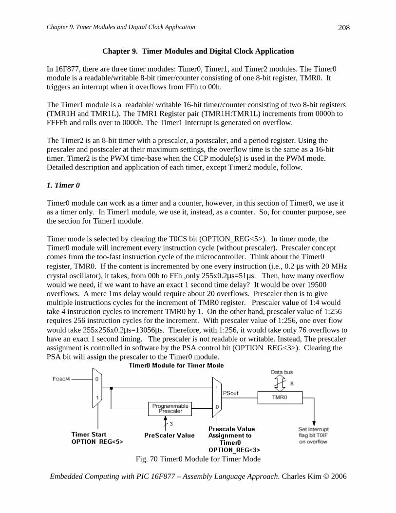
In 16F877, there are three timer modules: Timer0, Timer1, and Timer2 modules. The Timer0 module is a readable/writable 8-bit timer/counter consisting of one 8-bit register, TMR0. It triggers an interrupt when it overflows from FFh to 00h. The Timer1 module is a readable/ writable 16-bit timer/counter consisting of two 8-bit registers (TMR1H and TMR1L). The TMR1 Register pair (TMR1H:TMR1L) increments from 0000h to FFFFh and rolls over to 0000h. The Timer1 Interrupt is generated on overflow. The Timer2 is an 8-bit timer with a prescaler, a postscaler, and a period register. Using the prescaler and postscaler at their maximum settings, the overflow time is the same as a 16-bit timer. Timer2 is the PWM time-base when the CCP module(s) is used in the PWM mode. Detailed description and application of each timer, except Timer2 module, follow. 1. Timer 0 Timer0 module can work as a timer and a counter, however, in this section of Timer0, we use it as a timer only. In Timer1 module, we use it, instead, as a counter. So, for counter purpose, see the section for Timer1 module. Timer mode is selected by clearing the T0CS bit (OPTION_REG<5>). In timer mode, the Timer0 module will increment every instruction cycle (without prescaler). Prescaler concept comes from the too-fast instruction cycle of the microcontroller. Think about the Timer0 register, TMR0. If the content is incremented by one every instruction (i.e., 0.2 µs with 20 MHz crystal oscillator), it takes, from 00h to FFh ,only 255x0.2µs=51µs. Then, how many overflow would we need, if we want to have an exact 1 second time delay? It would be over 19500 overflows. A mere 1ms delay would require about 20 overflows. Prescaler then is to give multiple instructions cycles for the increment of TMR0 register. Prescaler value of 1:4 would take 4 instruction cycles to increment TMR0 by 1. On the other hand, prescaler value of 1:256 requires 256 instruction cycles for the increment. With prescaler value of 1:256, one over flow would take 255x256x0.2µs=13056µs. Therefore, with 1:256, it would take only 76 overflows to have an exact 1 second timing. The prescaler is not readable or writable. Instead, The prescaler assignment is controlled in software by the PSA control bit (OPTION_REG<3>). Clearing the PSA bit will assign the prescaler to the Timer0 module.
Fig. 70 Timer0 Module for Timer Mode
Chapter 9. Timer Modules and Digital Clock Application
Embedded Computing with PIC 16F877 – Assembly Language Approach. Charles Kim © 2006
209
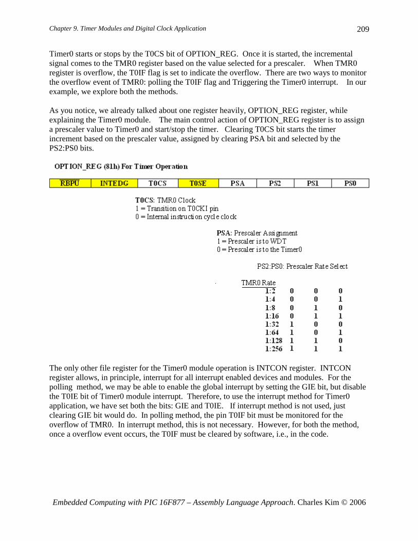
Timer0 starts or stops by the T0CS bit of OPTION_REG. Once it is started, the incremental signal comes to the TMR0 register based on the value selected for a prescaler. When TMR0 register is overflow, the T0IF flag is set to indicate the overflow. There are two ways to monitor the overflow event of TMR0: polling the T0IF flag and Triggering the Timer0 interrupt. In our example, we explore both the methods. As you notice, we already talked about one register heavily, OPTION_REG register, while explaining the Timer0 module. The main control action of OPTION_REG register is to assign a prescaler value to Timer0 and start/stop the timer. Clearing T0CS bit starts the timer increment based on the prescaler value, assigned by clearing PSA bit and selected by the PS2:PS0 bits.
The only other file register for the Timer0 module operation is INTCON register. INTCON register allows, in principle, interrupt for all interrupt enabled devices and modules. For the polling method, we may be able to enable the global interrupt by setting the GIE bit, but disable the T0IE bit of Timer0 module interrupt. Therefore, to use the interrupt method for Timer0 application, we have set both the bits: GIE and T0IE. If interrupt method is not used, just clearing GIE bit would do. In polling method, the pin T0IF bit must be monitored for the overflow of TMR0. In interrupt method, this is not necessary. However, for both the method, once a overflow event occurs, the T0IF must be cleared by software, i.e., in the code.
Chapter 9. Timer Modules and Digital Clock Application
Embedded Computing with PIC 16F877 – Assembly Language Approach. Charles Kim © 2006
210
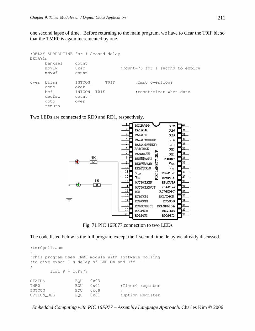
INTCON REGISTER (0Bh, 8Bh, 10Bh, 18Bh) for TIMER0 Operation
GIE PEIE T0IE INTE RBIE T0IF INTF RB1F GIE: Global Interrupt Enable bit 1 = Enables all unmasked interrupts 0 = Disables all interrupts T0IE: TMR0 Interrupt Enable bit 1 = Enables the TMR0 interrupt 0 = Disables the TNR0 interrupt T0IF: TMR0 Interrupt Flag bit 1 = TMR0 register has overflowed (must be cleared in software) 0 = TMR0 register did not overflow 2. Timer 0 Application 1 - LED Blinking Since we discussed about Timer0 module and necessary special function registers, it is about the time to apply this module. We will discuss two simple example cases of LED On and Off program. In our previous example of LED, we could build a time delay solely based on the number of instruction cycles for a given routine. In this section, we apply Timer0 module for the same purpose. To do this, we apply two different approaches as announced earlier: polling approach and interrupt approach. Timer0 Application with Polling Approach The polling approach is to monitor the T0IF bit of INTCON register for an overflow event in TMR0. For a desired delay, we would come up with how many overflows are necessary based upon the prescaler value. Here is a general procedure for the polling approach. 1. Assign the prescaler to Timer0 by clearing PSA bit (OPTION_REG<3>). 2. Select the desired prescale value by the 3 bits of OPTION_REG. (OPTION_REG<2:0>) 3.Clear TMR0 register and clear T0IF bit (INTCON<2>). 4.Turn on the timer by clearing T0CS bit (OPTION_REG<5>). 5.Poll T0IF for the timer overflow. The timer overflows when the value of TMR0 increments from 0xFF to 0x00. This sets T0IF. 6. If T0IF is set, clear it. Then, how do we get 1 second time delay? As we briefly discussed above, with 0.2µs of one instruction cycle time, we need 76 overflows of TMR0 when 1:256 prescaler value is selected. In the sample program, we will turn on an LED for 1 second while turning off the other LED, and vice versa, using the timer. Let's build the 1 second delay routine. The strategy is to decrease a temporary counting register COUNT from the magic number 76 every time the TMR0 overflow occurs. The subroutine expires when the COUNT reduces to zero, which will turn into
Chapter 9. Timer Modules and Digital Clock Application
Embedded Computing with PIC 16F877 – Assembly Language Approach. Charles Kim © 2006
211
one second lapse of time. Before returning to the main program, we have to clear the T0IF bit so that the TMR0 is again incremented by one.
;DELAY SUBROUTINE for 1 Second delayDELAY1s
banksel countmovlw 0x4c ;Count=76 for 1 second to expiremovwf count
over btfss INTCON, T0IF ;Tmr0 overflow?goto overbcf INTCON, T0IF ;reset/clear when donedecfsz countgoto overreturn
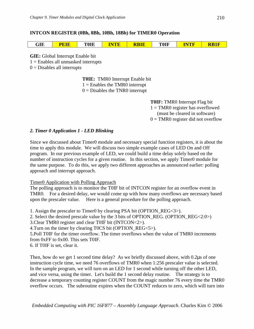
Two LEDs are connected to RD0 and RD1, respectively.
Fig. 71 PIC 16F877 connection to two LEDs
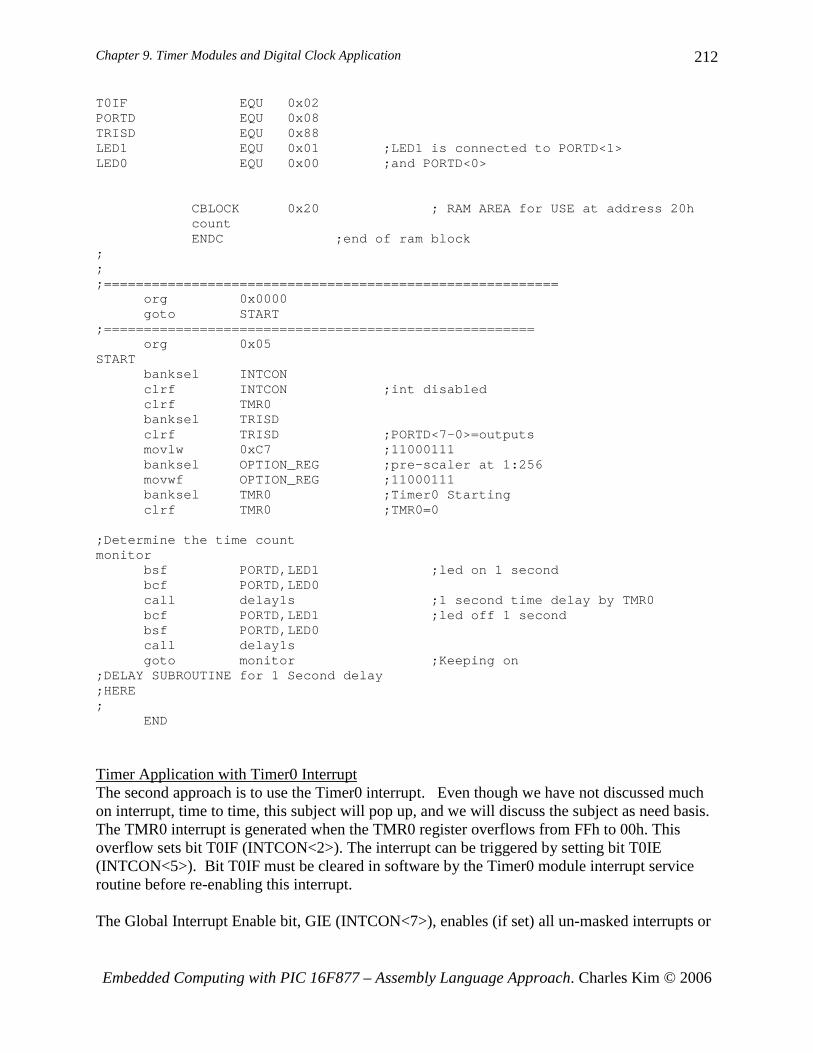
The code listed below is the full program except the 1 second time delay we already discussed. ;tmr0poll.asm;;This program uses TMR0 module with software polling;to give exact 1 s delay of LED On and Off;
list P = 16F877
STATUS EQU 0x03TMR0 EQU 0x01 ;Timer0 registerINTCON EQU 0x0B ;OPTION_REG EQU 0x81 ;Option Register
Chapter 9. Timer Modules and Digital Clock Application
Embedded Computing with PIC 16F877 – Assembly Language Approach. Charles Kim © 2006
212
T0IF EQU 0x02PORTD EQU 0x08TRISD EQU 0x88LED1 EQU 0x01 ;LED1 is connected to PORTD<1>LED0 EQU 0x00 ;and PORTD<0>
CBLOCK 0x20 ; RAM AREA for USE at address 20hcountENDC ;end of ram block
;;;=========================================================
org 0x0000goto START
;======================================================org 0x05
STARTbanksel INTCONclrf INTCON ;int disabledclrf TMR0banksel TRISDclrf TRISD ;PORTD<7-0>=outputsmovlw 0xC7 ;11000111banksel OPTION_REG ;pre-scaler at 1:256movwf OPTION_REG ;11000111banksel TMR0 ;Timer0 Startingclrf TMR0 ;TMR0=0
;Determine the time countmonitor
bsf PORTD,LED1 ;led on 1 secondbcf PORTD,LED0call delay1s ;1 second time delay by TMR0bcf PORTD,LED1 ;led off 1 secondbsf PORTD,LED0call delay1sgoto monitor ;Keeping on
;DELAY SUBROUTINE for 1 Second delay;HERE;
END
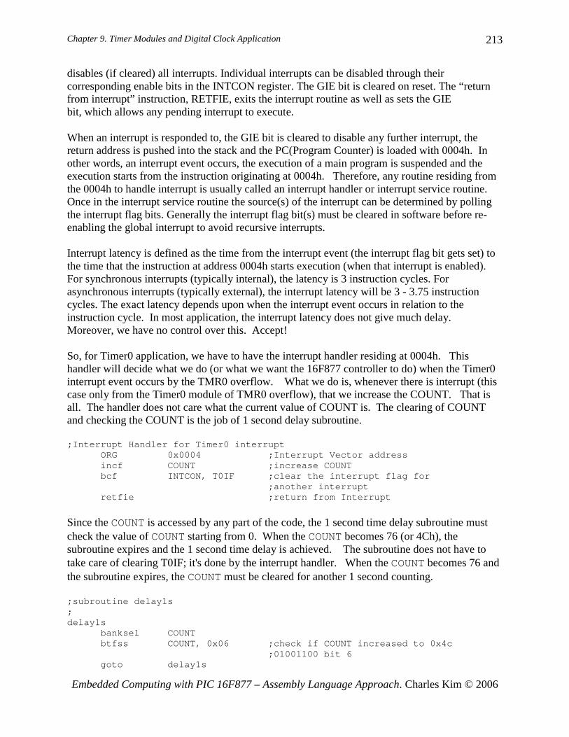
Timer Application with Timer0 Interrupt The second approach is to use the Timer0 interrupt. Even though we have not discussed much on interrupt, time to time, this subject will pop up, and we will discuss the subject as need basis. The TMR0 interrupt is generated when the TMR0 register overflows from FFh to 00h. This overflow sets bit T0IF (INTCON<2>). The interrupt can be triggered by setting bit T0IE (INTCON<5>). Bit T0IF must be cleared in software by the Timer0 module interrupt service routine before re-enabling this interrupt. The Global Interrupt Enable bit, GIE (INTCON<7>), enables (if set) all un-masked interrupts or
Chapter 9. Timer Modules and Digital Clock Application
Embedded Computing with PIC 16F877 – Assembly Language Approach. Charles Kim © 2006
213
disables (if cleared) all interrupts. Individual interrupts can be disabled through their corresponding enable bits in the INTCON register. The GIE bit is cleared on reset. The “return from interrupt” instruction, RETFIE, exits the interrupt routine as well as sets the GIE bit, which allows any pending interrupt to execute. When an interrupt is responded to, the GIE bit is cleared to disable any further interrupt, the return address is pushed into the stack and the PC(Program Counter) is loaded with 0004h. In other words, an interrupt event occurs, the execution of a main program is suspended and the execution starts from the instruction originating at 0004h. Therefore, any routine residing from the 0004h to handle interrupt is usually called an interrupt handler or interrupt service routine. Once in the interrupt service routine the source(s) of the interrupt can be determined by polling the interrupt flag bits. Generally the interrupt flag bit(s) must be cleared in software before re-enabling the global interrupt to avoid recursive interrupts. Interrupt latency is defined as the time from the interrupt event (the interrupt flag bit gets set) to the time that the instruction at address 0004h starts execution (when that interrupt is enabled). For synchronous interrupts (typically internal), the latency is 3 instruction cycles. For asynchronous interrupts (typically external), the interrupt latency will be 3 - 3.75 instruction cycles. The exact latency depends upon when the interrupt event occurs in relation to the instruction cycle. In most application, the interrupt latency does not give much delay. Moreover, we have no control over this. Accept! So, for Timer0 application, we have to have the interrupt handler residing at 0004h. This handler will decide what we do (or what we want the 16F877 controller to do) when the Timer0 interrupt event occurs by the TMR0 overflow. What we do is, whenever there is interrupt (this case only from the Timer0 module of TMR0 overflow), that we increase the COUNT. That is all. The handler does not care what the current value of COUNT is. The clearing of COUNT and checking the COUNT is the job of 1 second delay subroutine.
;Interrupt Handler for Timer0 interruptORG 0x0004 ;Interrupt Vector addressincf COUNT ;increase COUNTbcf INTCON, T0IF ;clear the interrupt flag for
;another interruptretfie ;return from Interrupt
Since the COUNT is accessed by any part of the code, the 1 second time delay subroutine must check the value of COUNT starting from 0. When the COUNT becomes 76 (or 4Ch), the subroutine expires and the 1 second time delay is achieved. The subroutine does not have to take care of clearing T0IF; it's done by the interrupt handler. When the COUNT becomes 76 and the subroutine expires, the COUNT must be cleared for another 1 second counting. ;subroutine delay1s;delay1s
banksel COUNTbtfss COUNT, 0x06 ;check if COUNT increased to 0x4c
;01001100 bit 6goto delay1s
Chapter 9. Timer Modules and Digital Clock Application
Embedded Computing with PIC 16F877 – Assembly Language Approach. Charles Kim © 2006
214
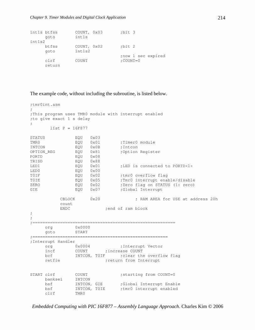
int1s btfss COUNT, 0x03 ;bit 3goto int1s
int1s2btfss COUNT, 0x02 ;bit 2goto int1s2
;now 1 sec expiredclrf COUNT ;COUNT=0return
The example code, without including the subroutine, is listed below. ;tmr0int.asm;;This program uses TMR0 module with interrupt enabled;to give exact 1 s delay;
list P = 16F877
STATUS EQU 0x03TMR0 EQU 0x01 ;Timer0 moduleINTCON EQU 0x0B ;IntconOPTION_REG EQU 0x81 ;Option RegisterPORTD EQU 0x08TRISD EQU 0x88LED1 EQU 0x01 ;LED is connected to PORTD<1>LED0 EQU 0x00T0IF EQU 0x02 ;tmr0 overflow flagT0IE EQU 0x05 ;Tmr0 interrupt enable/disableZERO EQU 0x02 ;Zero flag on STATUS (1: zero)GIE EQU 0x07 ;Global Interrupt
CBLOCK 0x20 ; RAM AREA for USE at address 20hcountENDC ;end of ram block
;;;=========================================================
org 0x0000goto START
;======================================================;Interrupt Handler
org 0x0004 ;Interrupt Vectorincf COUNT ;increase COUNTbcf INTCON, T0IF ;clear the overflow flagretfie ;return from Interrupt
START clrf COUNT ;starting from COUNT=0banksel INTCONbsf INTCON, GIE ;Global Interrupt Enablebsf INTCON, T0IE ;tmr0 interrupt enabledclrf TMR0
Chapter 9. Timer Modules and Digital Clock Application
Embedded Computing with PIC 16F877 – Assembly Language Approach. Charles Kim © 2006
215
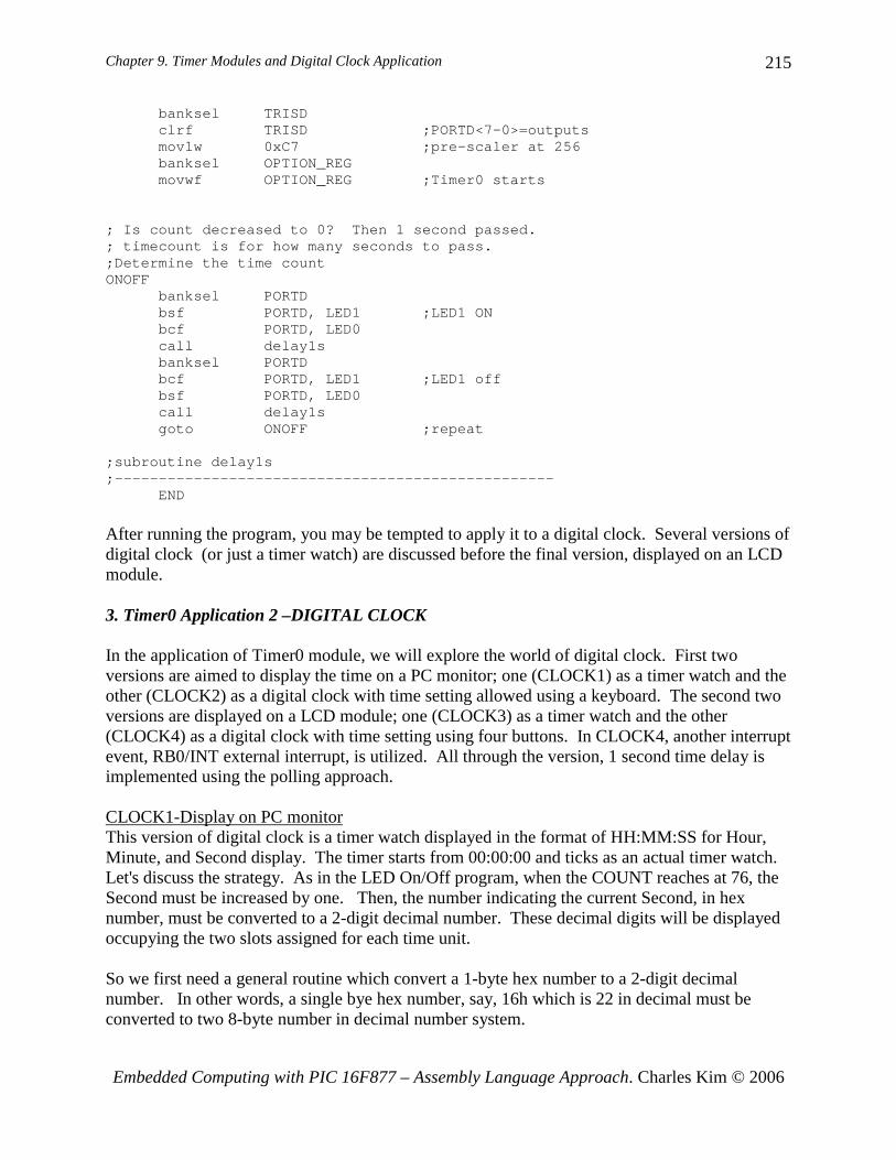
banksel TRISDclrf TRISD ;PORTD<7-0>=outputsmovlw 0xC7 ;pre-scaler at 256banksel OPTION_REGmovwf OPTION_REG ;Timer0 starts
; Is count decreased to 0? Then 1 second passed.; timecount is for how many seconds to pass.;Determine the time countONOFF
banksel PORTDbsf PORTD, LED1 ;LED1 ONbcf PORTD, LED0call delay1sbanksel PORTDbcf PORTD, LED1 ;LED1 offbsf PORTD, LED0call delay1sgoto ONOFF ;repeat
;subroutine delay1s;--------------------------------------------------
END After running the program, you may be tempted to apply it to a digital clock. Several versions of digital clock (or just a timer watch) are discussed before the final version, displayed on an LCD module. 3. Timer0 Application 2 –DIGITAL CLOCK In the application of Timer0 module, we will explore the world of digital clock. First two versions are aimed to display the time on a PC monitor; one (CLOCK1) as a timer watch and the other (CLOCK2) as a digital clock with time setting allowed using a keyboard. The second two versions are displayed on a LCD module; one (CLOCK3) as a timer watch and the other (CLOCK4) as a digital clock with time setting using four buttons. In CLOCK4, another interrupt event, RB0/INT external interrupt, is utilized. All through the version, 1 second time delay is implemented using the polling approach. CLOCK1-Display on PC monitor This version of digital clock is a timer watch displayed in the format of HH:MM:SS for Hour, Minute, and Second display. The timer starts from 00:00:00 and ticks as an actual timer watch. Let's discuss the strategy. As in the LED On/Off program, when the COUNT reaches at 76, the Second must be increased by one. Then, the number indicating the current Second, in hex number, must be converted to a 2-digit decimal number. These decimal digits will be displayed occupying the two slots assigned for each time unit. So we first need a general routine which convert a 1-byte hex number to a 2-digit decimal number. In other words, a single bye hex number, say, 16h which is 22 in decimal must be converted to two 8-byte number in decimal number system.
Chapter 9. Timer Modules and Digital Clock Application
Embedded Computing with PIC 16F877 – Assembly Language Approach. Charles Kim © 2006
216
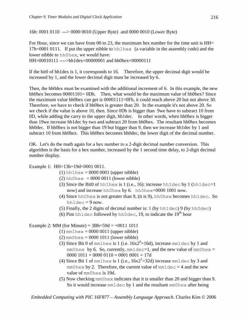
16h: 0001 0110 ---> 0000 0010 (Upper Byte) and 0000 0010 (Lower Byte) For Hour, since we can have from 00 to 23, the maximum hex number for the time unit is HH= 17h=0001 0111. If put the upper nibble to hh1hex (a variable in the assembly code) and the lower nibble to hh0hex, we would have: HH=00010111 ---->hh1dex=00000001 and hh0hex=00000111 If the bit0 of hh1dex is 1, it corresponds to 16. Therefore, the upper decimal digit would be increased by 1, and the lower decimal digit must be increased by 6. Then, the hh0dex must be examined with the additional increment of 6. In this example, the new hh0hex becomes 00001101= 0Dh. Then, what would be the maximum value of hh0hex? Since the maximum value hh0hex can get is 00001111=0Fh, it could reach above 20 but not above 30. Therefore, we have to check if hh0hex is greater than 20. In the example it's not above 20. So we check if the value is above 10, then. Since 0Dh is bigger than 9we have to subtract 10 from 0D, while adding the carry to the upper digit, hh1dec. In other words, when hh0hex is bigger than 19we increase hh1dec by two and subtract 20 from hh0hex. The resultant hh0hex becomes hh0dec. If hh0hex is not bigger than 19 but bigger than 9, then we increase hh1dec by 1 and subtract 10 from hh0hex. This hh0hex becomes hh0dec, the lower digit of the decimal number. OK. Let's do the math again for a hex number to a 2-digit decimal number conversion. This algorithm is the basis for a hex number, increased by the 1 second time delay, to 2-digit decimal number display. Example 1: HH=13h=19d=0001 0011.
(1) hh1hex = 0000 0001 (upper nibble) (2) hh0hex = 0000 0011 (lower nibble) (3) Since the Bit0 of hh1hex is 1 (i.e., 16): increase hh1dec by 1 (hh1dec=1
now) and increase hh0hex by 6. hh0hex=0000 1001 now. (4) Since hh0hex is not greater than 9, (it is 9), hh0hex becomes hh1dec. So
hh1dec = 9 now. (5) Finally, the 2 digits of decimal number is: 1 (by hh1dec) 9 (by hh0dec) (6) Pint hh1dec followed by hh0dec, 19, to indicate the 19th hour
Example 2: MM (for Minute) = 3Bh=59d = =0011 1011 (1) mm1hex = 0000 0011 (upper nibble) (2) mm0hex = 0000 1011 (lower nibble) (3) Since Bit 0 of mm1hex is 1 (i.e. 16x20=16d), increase mm1dec by 1 and
mm0hex by 6. So, currently, mm1dec=1, and the new value of mm0hex = 0000 1011 + 0000 0110 = 0001 0001 = 17d
(4) Since Bit 1 of mm1hex is 1 (i.e., 16x21=32d) increase mm1dec by 3 and mm0hex by 2. Therefore, the current value of mm1dec = 4 and the new value of mm0hex is 19d.
(5) Now checking mm0hex indicates that it is smaller than 20 and bigger than 9. So it would increase mm1dec by 1 and the resultant mm0hex after being
Chapter 9. Timer Modules and Digital Clock Application
Embedded Computing with PIC 16F877 – Assembly Language Approach. Charles Kim © 2006
217
subtracted by 10 is 9. Finally, mm1dec=5 and mm0dec =9. (6) Display the two digits, 5 and 9, to indicate the 59th minute.
Example 3: SS (for Second) = 1Fh=0001 1111 = 31d
(a) ss1hex = 0000 0001 (upper nibble) (b) ss0hex = 0000 1111 (lower nibble) (c) The bit0 of ss1hex is 1, therefore, 16x20=16, increase ss1dec by 1 and
ss0hex by 6. So the current value of ss1dec =1 and the new value of ss0hex is 15d+ 6d= 21d.
(c) Since hh0hex is bigger than 19, increase ss1dec by 2 to 3 and subtract 20 from hh0dex, which results in 1d as ss0dec.
(d) Therefore, the final values for ss1dec and ss0dec are 3 and 1, respectively.
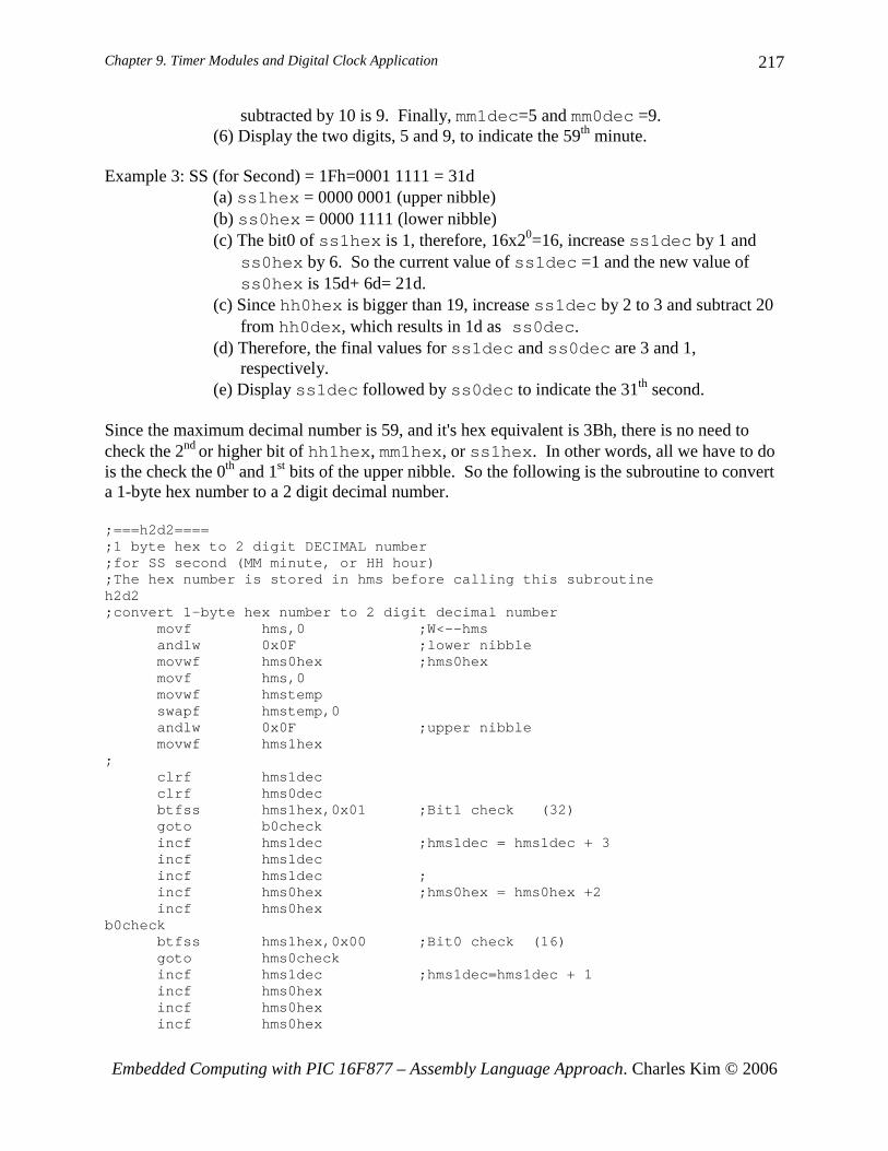
(e) Display ss1dec followed by ss0dec to indicate the 31th second. Since the maximum decimal number is 59, and it's hex equivalent is 3Bh, there is no need to check the 2nd or higher bit of hh1hex, mm1hex, or ss1hex. In other words, all we have to do is the check the 0th and 1st bits of the upper nibble. So the following is the subroutine to convert a 1-byte hex number to a 2 digit decimal number. ;===h2d2====;1 byte hex to 2 digit DECIMAL number;for SS second (MM minute, or HH hour);The hex number is stored in hms before calling this subroutineh2d2;convert 1-byte hex number to 2 digit decimal number
movf hms,0 ;W<--hmsandlw 0x0F ;lower nibblemovwf hms0hex ;hms0hexmovf hms,0movwf hmstempswapf hmstemp,0andlw 0x0F ;upper nibblemovwf hms1hex
;clrf hms1decclrf hms0decbtfss hms1hex,0x01 ;Bit1 check (32)goto b0checkincf hms1dec ;hms1dec = hms1dec + 3incf hms1decincf hms1dec ;incf hms0hex ;hms0hex = hms0hex +2incf hms0hex
b0checkbtfss hms1hex,0x00 ;Bit0 check (16)goto hms0checkincf hms1dec ;hms1dec=hms1dec + 1incf hms0hexincf hms0hexincf hms0hex
Chapter 9. Timer Modules and Digital Clock Application
Embedded Computing with PIC 16F877 – Assembly Language Approach. Charles Kim © 2006
218
incf hms0hexincf hms0hexincf hms0hex ;hms0hex = hms0hex + 6
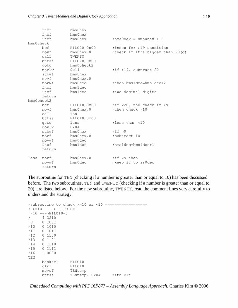
hms0checkbcf HILO20,0x00 ;index for >19 conditionmovf hms0hex,0 ;check if it's bigger than 20(d)call TWENTYbtfss HILO20,0x00goto hms0check2movlw 0x14 ;if >19, subtract 20subwf hms0hexmovf hms0hex,0movwf hms0dec ;then hms1dec=hms1dec+2incf hms1decincf hms1dec ;two decimal digitsreturn
hms0check2bcf HILO10,0x00 ;if <20, the check if >9movf hms0hex,0 ;then check >10call TENbtfss HILO10,0x00goto less ;less than <10movlw 0x0Asubwf hms0hex ;if >9movf hms0hex,0 ;subtract 10movwf hms0decincf hms1dec ;hms1dec=hms1dec+1return
less movf hms0hex,0 ;if <9 thenmovwf hms0dec ;keep it to ss0decreturn
The subroutine for TEN (checking if a number is greater than or equal to 10) has been discussed before. The two subroutines, TEN and TWENTY (checking if a number is greater than or equal to 20), are listed below. For the new subroutine, TWENTY, read the comment lines very carefully to understand the strategy. ;subroutine to check >=10 or <10 ==================; >=10 ---> HILO10=1;<10 --->HILO10=0; 4 3210;9 0 1001;10 0 1010;11 0 1011;12 0 1100;13 0 1101;14 0 1110;15 0 1111;16 1 0000TEN
banksel HILO10clrf HILO10movwf TENtempbtfss TENtemp, 0x04 ;4th bit
Chapter 9. Timer Modules and Digital Clock Application
Embedded Computing with PIC 16F877 – Assembly Language Approach. Charles Kim © 2006
219
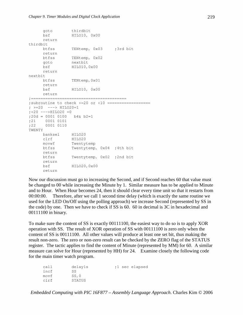
goto thirdbitbsf HILO10, 0x00return
thirdbitbtfss TENtemp, 0x03 ;3rd bitreturnbtfss TENtemp, 0x02goto nextbitbsf HILO10,0x00return
nextbitbtfss TENtemp,0x01returnbsf HILO10, 0x00return
;========================================;subroutine to check >=20 or <10 ==================; >=20 ---> HILO20=1;<20 --->HILO20 =0;20d = 0001 0100 b4& b2=1;21 0001 0101;22 0001 0110TWENTY
banksel HILO20clrf HILO20movwf Twentytempbtfss Twentytemp, 0x04 ;4th bitreturnbtfss Twentytemp, 0x02 ;2nd bitreturnbsf HILO20,0x00return
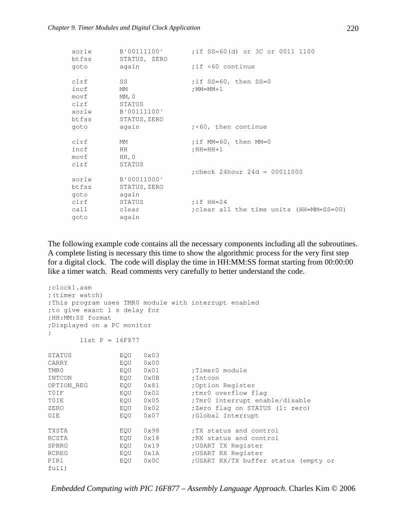
Now our discussion must go to increasing the Second, and if Second reaches 60 that value must be changed to 00 while increasing the Minute by 1. Similar measure has to be applied to Minute and to Hour. When Hour becomes 24, then it should clear every time unit so that it restarts from 00:00:00. Therefore, after we call 1 second time delay (which is exactly the same routine we used for the LED On/Off using the polling approach) we increase Second (represented by SS in the code) by one. Then we have to check if SS is 60. 60 in decimal is 3C in hexadecimal and 00111100 in binary. To make sure the content of SS is exactly 00111100, the easiest way to do so is to apply XOR operation with SS. The result of XOR operation of SS with 00111100 is zero only when the content of SS is 00111100. All other values will produce at least one set bit, thus making the result non-zero. The zero or non-zero result can be checked by the ZERO flag of the STATUS register. The tactic applies to find the content of Minute (represented by MM) for 60. A similar measure can solve for Hour (represented by HH) for 24. Examine closely the following code for the main timer watch program.
call delay1s ;1 sec elapsedincf SSmovf SS,0clrf STATUS
Chapter 9. Timer Modules and Digital Clock Application
Embedded Computing with PIC 16F877 – Assembly Language Approach. Charles Kim © 2006
220
xorlw B'00111100' ;if SS=60(d) or 3C or 0011 1100btfss STATUS, ZEROgoto again ;if <60 continue
clrf SS ;if SS=60, then SS=0incf MM ;MM=MM+1movf MM,0clrf STATUSxorlw B'00111100'btfss STATUS,ZEROgoto again ;<60, then continue
clrf MM ;if MM=60, then MM=0incf HH ;HH=HH+1movf HH,0clrf STATUS
;check 24hour 24d = 00011000xorlw B'00011000'btfss STATUS,ZEROgoto againclrf STATUS ;if HH=24call clear ;clear all the time units (HH=MM=SS=00)goto again
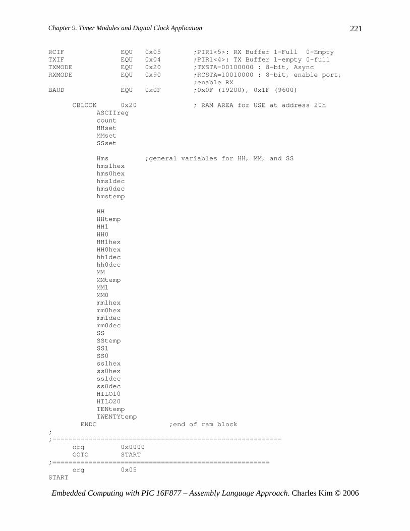
The following example code contains all the necessary components including all the subroutines. A complete listing is necessary this time to show the algorithmic process for the very first step for a digital clock. The code will display the time in HH:MM:SS format starting from 00:00:00 like a timer watch. Read comments very carefully to better understand the code.
;clock1.asm;(timer watch);This program uses TMR0 module with interrupt enabled;to give exact 1 s delay for;HH:MM:SS format;Displayed on a PC monitor;
list P = 16F877
STATUS EQU 0x03CARRY EQU 0x00TMR0 EQU 0x01 ;Timer0 moduleINTCON EQU 0x0B ;IntconOPTION_REG EQU 0x81 ;Option RegisterT0IF EQU 0x02 ;tmr0 overflow flagT0IE EQU 0x05 ;Tmr0 interrupt enable/disableZERO EQU 0x02 ;Zero flag on STATUS (1: zero)GIE EQU 0x07 ;Global Interrupt
TXSTA EQU 0x98 ;TX status and controlRCSTA EQU 0x18 ;RX status and controlSPBRG EQU 0x19 ;USART TX RegisterRCREG EQU 0x1A ;USART RX RegisterPIR1 EQU 0x0C ;USART RX/TX buffer status (empty orfull)
Chapter 9. Timer Modules and Digital Clock Application
Embedded Computing with PIC 16F877 – Assembly Language Approach. Charles Kim © 2006
221
RCIF EQU 0x05 ;PIR1<5>: RX Buffer 1-Full 0-EmptyTXIF EQU 0x04 ;PIR1<4>: TX Buffer 1-empty 0-fullTXMODE EQU 0x20 ;TXSTA=00100000 : 8-bit, AsyncRXMODE EQU 0x90 ;RCSTA=10010000 : 8-bit, enable port,
;enable RXBAUD EQU 0x0F ;0x0F (19200), 0x1F (9600)
CBLOCK 0x20 ; RAM AREA for USE at address 20hASCIIregcountHHsetMMsetSSset
Hms ;general variables for HH, MM, and SShms1hexhms0hexhms1dechms0dechmstemp
HHHHtempHH1HH0HH1hexHH0hexhh1dechh0decMMMMtempMM1MM0mm1hexmm0hexmm1decmm0decSSSStempSS1SS0ss1hexss0hexss1decss0decHILO10HILO20TENtempTWENTYtemp
ENDC ;end of ram block;;=========================================================
org 0x0000GOTO START
;======================================================org 0x05
START
Chapter 9. Timer Modules and Digital Clock Application
Embedded Computing with PIC 16F877 – Assembly Language Approach. Charles Kim © 2006
222
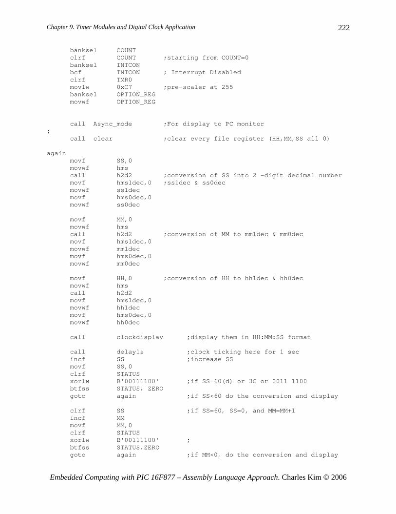
banksel COUNTclrf COUNT ;starting from COUNT=0banksel INTCONbcf INTCON ; Interrupt Disabledclrf TMR0movlw 0xC7 ;pre-scaler at 255banksel OPTION_REGmovwf OPTION_REG
call Async_mode ;For display to PC monitor;
call clear ;clear every file register (HH,MM,SS all 0)
againmovf SS,0movwf hmscall h2d2 ;conversion of SS into 2 –digit decimal numbermovf hms1dec,0 ;ss1dec & ss0decmovwf ss1decmovf hms0dec,0movwf ss0dec
movf MM,0movwf hmscall h2d2 ;conversion of MM to mm1dec & mm0decmovf hms1dec,0movwf mm1decmovf hms0dec,0movwf mm0dec
movf HH,0 ;conversion of HH to hh1dec & hh0decmovwf hmscall h2d2movf hms1dec,0movwf hh1decmovf hms0dec,0movwf hh0dec
call clockdisplay ;display them in HH:MM:SS format
call delay1s ;clock ticking here for 1 secincf SS ;increase SSmovf SS,0clrf STATUSxorlw B'00111100' ;if SS=60(d) or 3C or 0011 1100btfss STATUS, ZEROgoto again ;if SS<60 do the conversion and display
clrf SS ;if SS=60, SS=0, and MM=MM+1incf MMmovf MM,0clrf STATUSxorlw B'00111100' ;btfss STATUS,ZEROgoto again ;if MM<0, do the conversion and display
Chapter 9. Timer Modules and Digital Clock Application
Embedded Computing with PIC 16F877 – Assembly Language Approach. Charles Kim © 2006
223
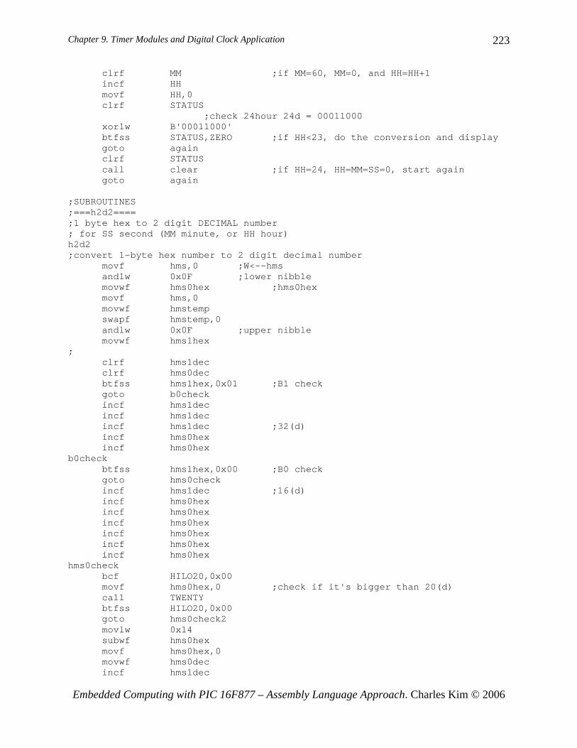
clrf MM ;if MM=60, MM=0, and HH=HH+1incf HHmovf HH,0clrf STATUS
;check 24hour 24d = 00011000xorlw B'00011000'btfss STATUS,ZERO ;if HH<23, do the conversion and displaygoto againclrf STATUScall clear ;if HH=24, HH=MM=SS=0, start againgoto again
;SUBROUTINES;===h2d2====;1 byte hex to 2 digit DECIMAL number; for SS second (MM minute, or HH hour)h2d2;convert 1-byte hex number to 2 digit decimal number
movf hms,0 ;W<--hmsandlw 0x0F ;lower nibblemovwf hms0hex ;hms0hexmovf hms,0movwf hmstempswapf hmstemp,0andlw 0x0F ;upper nibblemovwf hms1hex
;clrf hms1decclrf hms0decbtfss hms1hex,0x01 ;B1 checkgoto b0checkincf hms1decincf hms1decincf hms1dec ;32(d)incf hms0hexincf hms0hex
b0checkbtfss hms1hex,0x00 ;B0 checkgoto hms0checkincf hms1dec ;16(d)incf hms0hexincf hms0hexincf hms0hexincf hms0hexincf hms0hexincf hms0hex
hms0checkbcf HILO20,0x00movf hms0hex,0 ;check if it's bigger than 20(d)call TWENTYbtfss HILO20,0x00goto hms0check2movlw 0x14subwf hms0hexmovf hms0hex,0movwf hms0decincf hms1dec
Chapter 9. Timer Modules and Digital Clock Application
Embedded Computing with PIC 16F877 – Assembly Language Approach. Charles Kim © 2006
224
incf hms1dec ;two decimal digitsbcf HILO20,0x00return
hms0check2bcf HILO10,0x00movf hms0hex,0 ;then check >10call TENbtfss HILO10,0x00goto less ;less than <10movlw 0x0Asubwf hms0hexmovf hms0hex,0movwf hms0decincf hms1decreturn
less movf hms0hex,0movwf hms0dec ;so keep it to ss0decreturn
;end of h2d2 subroutine;;DELAY SUBROUTINE for 1 Second delay;DELAY1s
banksel countmovlw 0x4c ;Count=76 for 1 second to expiremovwf count
over btfss INTCON, T0IF ;Tmr0 overflow?goto overbcf INTCON, T0IF ;resetdecfsz countgoto overreturn
;--------------------------------------------------;RX TX Initialization with Asyc Mode;Async_mode SubroutineAsync_mode
banksel SPBRGmovlw baud ;B'00001111' (19200)movwf SPBRGbanksel TXSTAmovlw TXMODE ;B'00100000' Async Modemovwf TXSTAbanksel RCSTAmovlw RXMODE ;B'10010000' Enable Portmovwf RCSTAreturn
;RS232 TX subroutine ============TXPOLL
banksel PIR1btfss PIR1, TXIF ; Check if TX buffer is emptygoto TXPOLLbanksel TXREGmovwf TXREG ; Place the character to TX buffer
Chapter 9. Timer Modules and Digital Clock Application
Embedded Computing with PIC 16F877 – Assembly Language Approach. Charles Kim © 2006
225
return;-------------------------RXPOLL
banksel PIR1btfss PIR1, RCIF ;RX Buffer Full? (i.e. Data Received?)goto RXPOLLbanksel RCREGmovf RCREG,0 ;received data to Wreturn
;;To send CR ===============CR
movlw H'0d' ;CRcall TXPOLLreturn
;To send CR and LF ===============CRLF
movlw H'0d' ;CRcall TXPOLLmovlw H'0a' ;LFcall TXPOLLreturn
;subroutine to check >=10 or <10 ==================; >=10 ---> HILO10=1;<10 --->HILO10=0TEN
banksel HILO10clrf HILO10movwf TENtempbtfss TENtemp, 0x04 ;4th bitgoto thirdbitbsf HILO10, 0x00return
thirdbitbtfss TENtemp, 0x03 ;3rd bitreturnbtfss TENtemp, 0x02goto nextbitbsf HILO10,0x00return
nextbitbtfss TENtemp,0x01returnbsf HILO10, 0x00return
;subroutine to check >=20 or <10 ==================; >=20 ---> HILO20=1;<20 --->HILO20 =0;20d = 0001 0100 b4& b2=1TWENTY
banksel HILO20clrf HILO20movwf Twentytempbtfss Twentytemp, 0x04 ;4th bitreturnbtfss Twentytemp, 0x02 ;2nd bitreturn
Chapter 9. Timer Modules and Digital Clock Application
Embedded Computing with PIC 16F877 – Assembly Language Approach. Charles Kim © 2006
226
bsf HILO20,0x00return
;;subroutine CLOCKDISPLAYclockdisplay
banksel hh1decmovlw 0x30 ;To all digits add 30h to convert to ASCIIaddwf hh1decaddwf hh0decaddwf mm1decaddwf mm0decaddwf ss1decaddwf ss0dec
movf hh1dec,0call TXPOLLmovf hh0dec,0call TXPOLLmovlw ':'call TXPOLL ;:
movf mm1dec,0call TXPOLLmovf mm0dec,0call TXPOLLmovlw ':'call TXPOLL ;:
movf ss1dec,0call TXPOLLmovf ss0dec,0call TXPOLLcall CRreturn
;========================================;clock clear-reset subroutineclear
clrf STATUSbanksel SSmovlw 0x00 ;W=0clrf HHclrf MMclrf SS
clrf hh1hexclrf hh0hexclrf hh1decclrf hh0dec
clrf mm1hexclrf mm0hexclrf mm1decclrf mm0dec
clrf ss1hexclrf ss0hexclrf ss1dec
Chapter 9. Timer Modules and Digital Clock Application
Embedded Computing with PIC 16F877 – Assembly Language Approach. Charles Kim © 2006
227
clrf ss0decclrf hmsreturn
END;END of the code
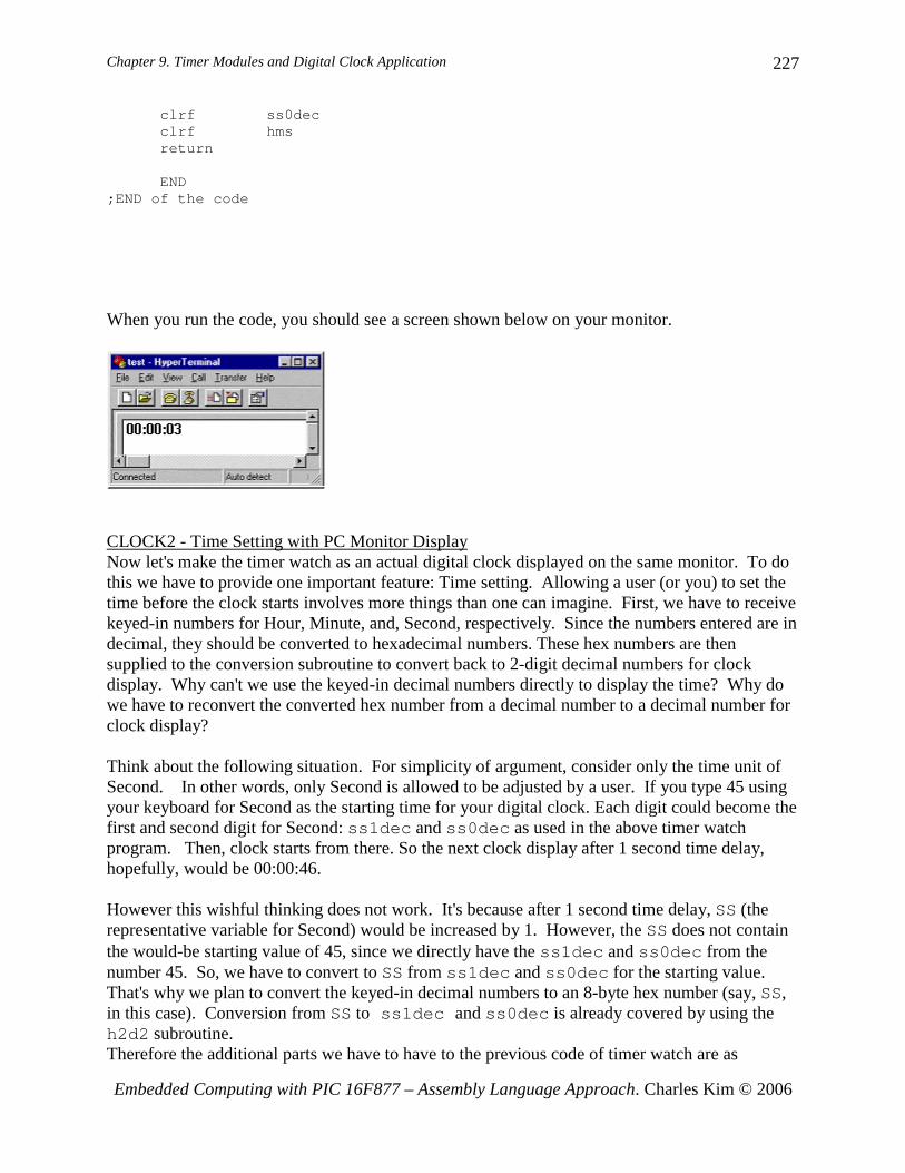
When you run the code, you should see a screen shown below on your monitor.
CLOCK2 - Time Setting with PC Monitor Display Now let's make the timer watch as an actual digital clock displayed on the same monitor. To do this we have to provide one important feature: Time setting. Allowing a user (or you) to set the time before the clock starts involves more things than one can imagine. First, we have to receive keyed-in numbers for Hour, Minute, and, Second, respectively. Since the numbers entered are in decimal, they should be converted to hexadecimal numbers. These hex numbers are then supplied to the conversion subroutine to convert back to 2-digit decimal numbers for clock display. Why can't we use the keyed-in decimal numbers directly to display the time? Why do we have to reconvert the converted hex number from a decimal number to a decimal number for clock display? Think about the following situation. For simplicity of argument, consider only the time unit of Second. In other words, only Second is allowed to be adjusted by a user. If you type 45 using your keyboard for Second as the starting time for your digital clock. Each digit could become the first and second digit for Second: ss1dec and ss0dec as used in the above timer watch program. Then, clock starts from there. So the next clock display after 1 second time delay, hopefully, would be 00:00:46. However this wishful thinking does not work. It's because after 1 second time delay, SS (the representative variable for Second) would be increased by 1. However, the SS does not contain the would-be starting value of 45, since we directly have the ss1dec and ss0dec from the number 45. So, we have to convert to SS from ss1dec and ss0dec for the starting value. That's why we plan to convert the keyed-in decimal numbers to an 8-byte hex number (say, SS, in this case). Conversion from SS to ss1dec and ss0dec is already covered by using the h2d2 subroutine. Therefore the additional parts we have to have to the previous code of timer watch are as
Chapter 9. Timer Modules and Digital Clock Application
Embedded Computing with PIC 16F877 – Assembly Language Approach. Charles Kim © 2006
228
follows: a. Reading keyed-in decimal number for Hour, Minute, and Second. b. Conversion of the keyed-in decimal numbers to 1-byte hex numbers (to HH, MM, and SS) c. Starting the clock using them as starting values. We need a detailed discussion on the first two parts. The format we want to use for time setting is that we type HH: as a prompt for a user to set the Hour. At the next line, we prompt MM: for the Minute. And at the third line would prompt SS: for the Second. Then at the fourth line, the clock with the set values would start. Reading the keyed-in decimal numbers is rather an easy task. The serial reception we once studied can be easily applied to receive any keyed-in characters. The following is the subroutine for keyed-in reading for time setting, timeset. It does not involve much complexity.
;subroutine;time set prompt and receptiontimeset
call CRLF ;move to the next line as the startermovlw 'H'call TXPOLLmovlw 'H'call TXPOLLmovlw ':'call TXPOLL ;HH: as typed
call RXPOLL ;read the first digit, hh1dexcall TXPOLL ;echo the keyed-in number
;subwf f - W --->dmovwf hh1hexmovlw 0x30subwf hh1hex ;convert from ASCII to hex number
call RXPOLL ;read the second digit, hh0hexcall TXPOLL ;echomovwf hh0hexmovlw 0x30 ;hh0hex=hh0hex-30hsubwf hh0hex ;conversion to hex from ASCII
call CRLF ;move to the next line
movlw 'M'call TXPOLLmovlw 'M'call TXPOLLmovlw ':'call TXPOLL ;MM: promptedcall RXPOLL ;read the first digit mm1hexcall TXPOLL ;echomovwf mm1hexmovlw 0x30subwf mm1hex ;ASCII to HEX
call RXPOLL ;read the second digit, mm0hexcall TXPOLL ;echomovwf mm0hex
Chapter 9. Timer Modules and Digital Clock Application
Embedded Computing with PIC 16F877 – Assembly Language Approach. Charles Kim © 2006
229
movlw 0x30 ;ASCII --> HEXsubwf mm0hex
call CRLF ;move to the next line
movlw 'S'call TXPOLLmovlw 'S'call TXPOLLmovlw ':'call TXPOLL ;SS: promptedcall RXPOLL ;ss1hexcall TXPOLL ;echomovwf ss1hexmovlw 0x30subwf ss1hex ;To HEX from ASCII
call RXPOLL ;ss0hexcall TXPOLL ;echomovwf ss0hexmovlw 0x30subwf ss0hex
call CRLF ;move to the next linereturn
;RS232 TX and RX subroutines ============TXPOLL
banksel PIR1btfss PIR1, TXIF ; Check if TX buffer is emptygoto TXPOLLbanksel TXREGmovwf TXREG ; Place the character to TX bufferreturn
;-------------------------RXPOLL
banksel PIR1btfss PIR1, RCIF ;RX Buffer Full? (i.e. Data Received?)goto RXPOLLbanksel RCREGmovf RCREG,0 ;received data to Wreturn
The next thing we will discuss is the conversion of the keyed-in decimal numbers to 1-byte hex numbers (to HH, MM, and SS). The objective of the discussion is how to convert the 2-digit decimal numbers, for example hh1hex and hh0hex, to the 1-byte hex number HH. Let's start with an example for HH (and hh1hex and hh0hex). Since the maximum number we get from the upper (or 10) digit hh1hex is 2, i.e., 0000 0010, therefore 0000 0010 should be interpreted as 20d (or 14h) while 0000 0011 as 10d (or 0Ah). The sum of this interpreted number and the lower (or unit) digit hh0hex would make HH, the hex number equivalent.
We can get a general interpretation rule of the upper digit as follows: ∑ ⋅⋅=
7
0102
n
nnk , where kn is
Chapter 9. Timer Modules and Digital Clock Application
Embedded Computing with PIC 16F877 – Assembly Language Approach. Charles Kim © 2006
230
the binary value of the nth bit of the digit. Of course, since we are dealing with a digital clock, For MM (and mm1hex and mm0hex) and SS (and ss1hex and ss0hex), since the maximum number for the upper digit mm1hex (or ss1hex) is 5, i.e., 0000 0101, the number n goes only to 2 from the formula. By the way, a number 0000 0101, using the formula above, is interpreted to:
50102110201021102 2102
0=⋅⋅+⋅⋅+⋅⋅=∑ ⋅⋅
=n
nnk
Then, how do we apply this formula for upper digit in the 17F877 coding? Directly applying the formula to a code is too luxurious to the microcontroller. However, we can indirectly apply the formula by testing kn, the nth bit of the digit and multiplying by (10x2n). The following subroutine, d22h, is to apply the formula to convert a 2-digit decimal number into a 1-byte hex number. After examining the subroutine, try to make the subroutine simpler by making a part of the code as another subroutine, and apply the same procedure to Hour, Minute, and Second processing. ;subroutine;conversion of decimal two digits to 1-byte hex numberd22h;HOUR FIRST
movlw 0x00btfss hh1hex,0x01 ;bit1 check for HOURgoto hnext1addlw 0x14 ;if bit1=1, +20
hnext1btfss hh1hex,0x00 ;bit0 checkgoto hnext2addlw 0x0A ;if bit0=1, +10
hnext2movwf HHmovf hh0hex,0 ;+hh0hex the lower digitaddwf HH ;total sum
;end of HH calculation
;MINUTE NEXTmovlw 0x00btfss mm1hex,0x00 ;bit0 check MINUTEgoto mnext1addlw 0x0A ;+10
mnext1btfss mm1hex,0x01 ;bit1 checkgoto mnext2addlw 0x14 ;+20
mnext2btfss mm1hex, 0x02 ;bit2 checkgoto mnext3addlw 0x28 ;+40
mnext3movwf MMmovf mm0hex, 0
Chapter 9. Timer Modules and Digital Clock Application
Embedded Computing with PIC 16F877 – Assembly Language Approach. Charles Kim © 2006
231
addwf MM ;total sum in hex
;For SECONDmovlw 0x00btfss ss1hex,0x00 ;bit0 check for SECONDgoto snext1addlw 0x0A ;+10
snext1btfss ss1hex,0x01 ;bit1 checkgoto snext2addlw 0x14 ;+20
snext2btfss ss1hex, 0x02 ;bit2 checkgoto snext3addlw 0x28 ;+40
snext3movwf SSmovf ss0hex, 0addwf SS ;total sum in hex
return
The following code is the main part of the CLOCK2 program. No subroutine is listed. Also, the block of variables (registers) defined from the address 20h is also omitted. The CBLOCK...ENDC part is the same as the one we used in CLOCK1 program. ; clock2.asm;;Clock program;Time setting allowed;Display format of HH:MM:SS;Displayed on a PC monitor;
list P = 16F877
STATUS EQU 0x03CARRY EQU 0x00TMR0 EQU 0x01 ;Timer0 moduleINTCON EQU 0x0B ;IntconOPTION_REG EQU 0x81 ;Option RegisterT0IF EQU 0x02 ;tmr0 overflow flagT0IE EQU 0x05 ;Tmr0 interrupt enable/disableZERO EQU 0x02 ;Zero flag on STATUS (1: zero)GIE EQU 0x07 ;Global Interrupt
TXSTA EQU 0x98 ;TX status and controlRCSTA EQU 0x18 ;RX status and controlSPBRG EQU 0x99 ;Baud Rate assignmentTXREG EQU 0x19 ;USART TX RegisterRCREG EQU 0x1A ;USART RX RegisterPIR1 EQU 0x0C ;USART RX/TX buffer status (empty orfull)RCIF EQU 0x05 ;PIR1<5>: RX Buffer 1-Full 0-EmptyTXIF EQU 0x04 ;PIR1<4>: TX Buffer 1-empty 0-full
Chapter 9. Timer Modules and Digital Clock Application
Embedded Computing with PIC 16F877 – Assembly Language Approach. Charles Kim © 2006
232
TXMODE EQU 0x20 ;TXSTA=00100000 : 8-bit, AsyncRXMODE EQU 0x90 ;RCSTA=10010000 : 8-bit, enable port,
; enable RXBAUD EQU 0x0F ;0x0F (19200), 0x1F (9600)
CBLOCK 0x20 ; RAM AREA for USE at address 20h;NOTE THAT THIS PORTION MUST BE COPIED FROM CLOCK1.ASM CODE;FOR A SUCCESSFUL COMPILING
ENDC ;end of ram block;;;;=========================================================
org 0x0000GOTO STARTorg 0x05
;======================================================
STARTbanksel INTCONclrf INTCON ;int disabledclrf TMR0banksel OPTION_REG ;pre-scaler at 256movwf OPTION_REG ;11000111banksel TMR0clrf TMR0
call Async_mode ;RX-232;
call clear ;clear every file registerbegin;display clock reset prompt
call timeset ;time adjustment;;conversion of decimal two digits to 1-byte hex number
call d22h;again
movf SS,0movwf hmscall h2d2movf hms1dec,0movwf ss1decmovf hms0dec,0movwf ss0dec
movf MM,0movwf hmscall h2d2movf hms1dec,0movwf mm1decmovf hms0dec,0movwf mm0dec
movf HH,0movwf hmscall h2d2
Chapter 9. Timer Modules and Digital Clock Application
Embedded Computing with PIC 16F877 – Assembly Language Approach. Charles Kim © 2006
233
movf hms1dec,0movwf hh1decmovf hms0dec,0movwf hh0dec
call clockdisplaycall delay1sincf SSmovf SS,0clrf STATUSxorlw B'00111100' ;if SS=60(d) or 3C or 0011 1100btfss STATUS, ZEROgoto again
clrf SSincf MMmovf MM,0clrf STATUSxorlw B'00111100'btfss STATUS,ZEROgoto again
clrf MMincf HHmovf HH,0clrf STATUS
;check 24hour 24d = 00011000xorlw B'00011000'btfss STATUS,ZEROgoto againclrf STATUScall cleargoto again
;SUBROUTINES HERE;
END
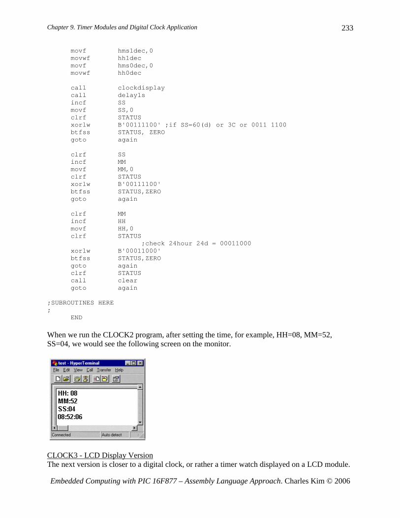
When we run the CLOCK2 program, after setting the time, for example, HH=08, MM=52, SS=04, we would see the following screen on the monitor.
CLOCK3 - LCD Display Version The next version is closer to a digital clock, or rather a timer watch displayed on a LCD module.
Chapter 9. Timer Modules and Digital Clock Application
Embedded Computing with PIC 16F877 – Assembly Language Approach. Charles Kim © 2006
234
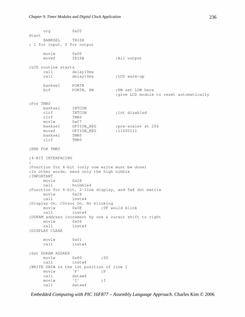
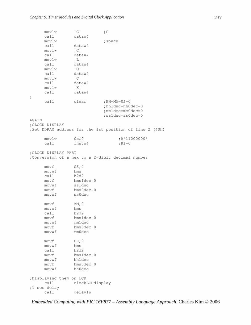
We use the 20x4 LCD module we already used for the previous example programming. For this timer watch example, we will stick to 4-bit interface configuration. If you lost most of the gains on LCD, go back to the proper section and code for better understand this section. The final result of CLCOK3 on LCD is to display HH:MM:SS format display without time setting features. Therefore, it would start from 00:00:00 at the second line of the LCD screen. The first line of the LCD would display 'PIC CLOCK' as a logo. Since we already have necessary subroutines, the primary task is to send the calculated digits of time units to LCD not to the PC monitor. Therefore, we have to change the subroutine clockdisplay which is for PC monitor to clockLCDdisplay for LCD. Basically this change comprises most of the changes we need for displaying on LCD. All the other subroutines are the same as we used from CLOCK1 and CLOCK2. Remember the two subroutines we developed for LCD: instruction write for 4-bit interface (instw4) and data write for 4-bit interface (dataw4). ;subroutin CLOCKLCDDISPLAYclockLCDdisplay
banksel hh1decmovlw 0x30addwf hh1dec ;ASCII conversionaddwf hh0decaddwf mm1decaddwf mm0decaddwf ss1decaddwf ss0decmovf hh1dec,0call dataw4 ;hh1dec write to LCDmovf hh0dec,0call dataw4 ;hh0dec write to LCDmovlw ':'call dataw4 ;: followsmovf mm1dec,0call dataw4movf mm0dec, 0call dataw4movlw ':'call dataw4movf ss1dec,0call dataw4movf ss0dec,0call dataw4return
The example code listed below comes with only main part: subroutines are omitted since we already discussed them before. As before, the CBLOCK..ENDC part is also omitted since it is the same block we used for CLOCK1. ;clock3.asm;;DIGITAL CLOCK ON LCD; NO BUTTONS FOR TIME SETTING
Chapter 9. Timer Modules and Digital Clock Application
Embedded Computing with PIC 16F877 – Assembly Language Approach. Charles Kim © 2006
235
;20x4 LCD module;by Truly (HD44780 compatible);; 4-bit interfacing;; Pin Connection from LCD to 16F877; LCD (pin#) 16F877 (pin#);DB7 (14) -----RB7(40);DB6 (13) ----RB6(39);DB5 (12) ----RB5(38);DB4 (11) ----RB4(37);DB3 (10);DB2 (9);DB1 (8);DB0 (7);E (6) ------RB2(35);RW (5) -----RB3(36);RS (4) -----RB1(24);Vo (3) -----GND;Vdd (2) ----+5V;Vss (1) -----GND;;Example clcok display:; PIC CLOCK (1st line); HH:MM:SS (2nd line);
list P = 16F877
STATUS EQU 0x03PORTB EQU 0x06TRISB EQU 0x86RS EQU 0x01 ;RB1E EQU 0x02 ;RB2RW EQU 0x03 ;RB3CARRY EQU 0x00TMR0 EQU 0x01 ;Timer0 moduleINTCON EQU 0x0B ;IntconOPTION_REG EQU 0x81 ;Option RegisterT0IF EQU 0x02 ;tmr0 overflow flagT0IE EQU 0x05 ;Tmr0 interrupt enable/disableZERO EQU 0x02 ;Zero flag on STATUS (1: zero)GIE EQU 0x07 ;Global Interrupt;RAM
CBLOCK 0x20;NOTE INCLUDE THE VARIABLES (FILE REGISTERS) HERE;
ENDC
;program should start from 0005h;0004h is allocated to interrupt handler
org 0x0000goto START
Chapter 9. Timer Modules and Digital Clock Application
Embedded Computing with PIC 16F877 – Assembly Language Approach. Charles Kim © 2006
236
org 0x05Start
BANKSEL TRISB; 1 for input, 0 for output
movlw 0x00movwf TRISB ;All output
;LCD routine startscall delay10mscall delay10ms ;LCD warm-up
banksel PORTBbcf PORTB, RW ;RW set LOW here
;give LCD module to reset automatically
;For TMR0banksel INTCONclrf INTCON ;int disabledclrf TMR0movlw 0xC7banksel OPTION_REG ;pre-scaler at 256movwf OPTION_REG ;11000111banksel TMR0clrf TMR0
;END FOR TMR0
;4-BIT INTERFACING;;Function for 4-bit (only one write must be done);In other words, send only the high nibble;IMPORTANT
movlw 0x28call hnibble4
;Function for 4-bit, 2-line display, and 5x8 dot matrixmovlw 0x28call instw4
;Display On, CUrsor On, No blinkingmovlw 0x0E ;0F would blinkcall instw4
;DDRAM address increment by one & cursor shift to rightmovlw 0x06call instw4
;DISPLAY CLEAR
movlw 0x01call instw4
;Set DDRAM ADDRESmovlw 0x80 ;00call instw4
;WRITE DATA in the 1st position of line 1movlw 'P' ;Pcall dataw4movlw 'I' ;Icall dataw4
Chapter 9. Timer Modules and Digital Clock Application
Embedded Computing with PIC 16F877 – Assembly Language Approach. Charles Kim © 2006
237
movlw 'C' ;Ccall dataw4movlw ' ' ;spacecall dataw4movlw 'C'call dataw4movlw 'L'call dataw4movlw 'O'call dataw4movlw 'C'call dataw4movlw 'K'call dataw4
;call clear ;HH=MM=SS=0
;hh1dec=hh0dec=0;mm1dec=mm0dec=0;ss1dec=ss0dec=0
AGAIN;CLOCK DISPLAY;Set DDRAM address for the 1st position of line 2 (40h)
movlw 0xC0 ;B'11000000'call instw4 ;RS=0
;CLOCK DISPLAY PART;Conversion of a hex to a 2-digit decimal number
movf SS,0movwf hmscall h2d2movf hms1dec,0movwf ss1decmovf hms0dec,0movwf ss0dec
movf MM,0movwf hmscall h2d2movf hms1dec,0movwf mm1decmovf hms0dec,0movwf mm0dec
movf HH,0movwf hmscall h2d2movf hms1dec,0movwf hh1decmovf hms0dec,0movwf hh0dec
;Displaying them on LCDcall clockLCDdisplay
;1 sec delaycall delay1s
Chapter 9. Timer Modules and Digital Clock Application
Embedded Computing with PIC 16F877 – Assembly Language Approach. Charles Kim © 2006
238
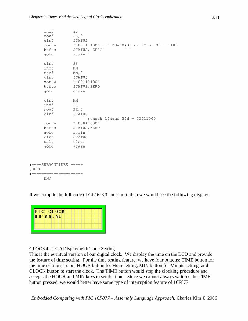
incf SSmovf SS,0clrf STATUSxorlw B'00111100' ;if SS=60(d) or 3C or 0011 1100btfss STATUS, ZEROgoto again
clrf SSincf MMmovf MM,0clrf STATUSxorlw B'00111100'btfss STATUS,ZEROgoto again
clrf MMincf HHmovf HH,0clrf STATUS
;check 24hour 24d = 00011000xorlw B'00011000'btfss STATUS,ZEROgoto againclrf STATUScall cleargoto again
;====SUBROUTINES =====;HERE;=====================
END
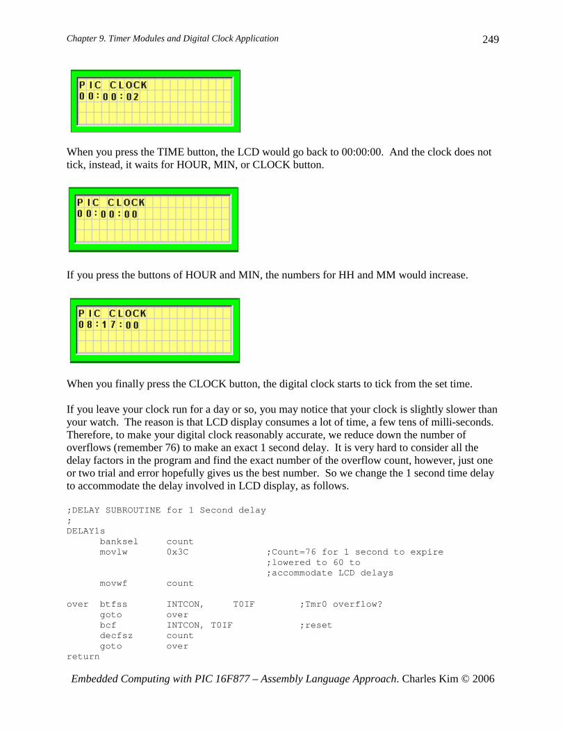
If we compile the full code of CLOCK3 and run it, then we would see the following display.
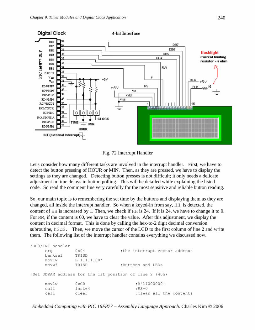
CLOCK4 - LCD Display with Time Setting This is the eventual version of our digital clock. We display the time on the LCD and provide the feature of time setting. For the time setting feature, we have four buttons: TIME button for the time setting session, HOUR button for Hour setting, MIN button for Minute setting, and CLOCK button to start the clock. The TIME button would stop the clocking procedure and accepts the HOUR and MIN keys to set the time. Since we cannot always wait for the TIME button pressed, we would better have some type of interruption feature of 16F877.
Chapter 9. Timer Modules and Digital Clock Application
Embedded Computing with PIC 16F877 – Assembly Language Approach. Charles Kim © 2006
239
As discussed early in this chapter, interrupt is a useful feature that allows the main program can proceed without keeping eye on the event. Since the button triggered signal comes from outside (external) of 16F877, we consider the RB0/INT interrupt. As the name implies, the RB0 pin (PORTB<0>) has a dual use: regular I/O pin as RB0 and external interrupt (INT) source. This interrupt can be enabled by setting the INT enable bit INTE (INTCON<4>). External interrupt on the RB0/INT pin is edge triggered, either rising, if INTEDG bit (OPTION_REG<6>) is set, or falling, if the INTEDG bit is clear. When a valid edge appears on the RB0/INT pin, flag bit INTF (INTCON<1>) is set. Flag bit INTF must be cleared in software (i.e., in the code) in the interrupt service routine before re-enabling this interrupt. The interrupt handler then should do a lot of work: (i) reading the HOUR and MIN buttons, (ii) increasing the corresponding hex numbers for Hour and Minute, and (iii) reading CLOCK button to expire the interrupt handler. The main routine is not much different from CLOCK3: it displays the contents of HH, MM, and SS (after hex to decimal conversion) no matter what the contents are. The only change includes the necessary accommodation for PORTB for buttons and one LED attached at PORTD for indication purpose. This LED will be turned on as far as the interrupt handler is being processed. The CLOCK button would turn off the LED and clock starts. The circuit diagram for CLOCK4 is illustrated below. The TIME button is connected to RB0/INT pin, and HOUR, MIN, and CLOCK buttons are connected to RD5, RD4, and RD2, respectively. The outputs from the buttons, when not pressed, are High, and when pressed, the outputs experience a High-to-Low transition. Therefore, the proper set-up for INTEDG is 'clear'. Let's now discuss about the interrupt handler. As discussed, when the TIME button is pressed the RB0/INT pin experiences the High-to-Low transition and this triggers the INT interrupt. Then the Program Counter (PC) is changed to 0004h where the interrupt handler is residing. A TIME button would clear the contents of the time units, and fill them with new values according to the HOUR and MIN buttons. One click of HOUR or MIN would increase the value by 1 and we display the content on LCD.
Chapter 9. Timer Modules and Digital Clock Application
Embedded Computing with PIC 16F877 – Assembly Language Approach. Charles Kim © 2006
240
Fig. 72 Interrupt Handler Let's consider how many different tasks are involved in the interrupt handler. First, we have to detect the button pressing of HOUR or MIN. Then, as they are pressed, we have to display the settings as they are changed. Detecting button presses is not difficult; it only needs a delicate adjustment in time delays in button polling. This will be detailed while explaining the listed code. So read the comment line very carefully for the most sensitive and reliable button reading. So, our main topic is to remembering the set time by the buttons and displaying them as they are changed, all inside the interrupt handler. So when a keyed-in from say, HH, is detected, the content of HH is increased by 1. Then, we check if HH is 24. If it is 24, we have to change it to 0. For MM, if the content is 60, we have to clear the value. After this adjustment, we display the content in decimal format. This is done by calling the hex-to-2 digit decimal conversion subroutine, h2d2. Then, we move the cursor of the LCD to the first column of line 2 and write them. The following list of the interrupt handler contains everything we discussed now. ;RB0/INT handler
org 0x04 ;the interrupt vector addressbanksel TRISDmovlw B'11111100'movwf TRISD ;Buttons and LEDs
;Set DDRAM address for the 1st position of line 2 (40h)
movlw 0xC0 ;B'11000000'call instw4 ;RS=0call clear ;clear all the contents
Chapter 9. Timer Modules and Digital Clock Application
Embedded Computing with PIC 16F877 – Assembly Language Approach. Charles Kim © 2006
241
call clockLCDdisplay ;Display 00:00:00;as the time setting starts
banksel PORTDbsf PORTD,0x01 ;INT indicator oncall delay10ms
;CLOCK ADJUSTMENT ROUTINE;Check for HOUR or MIN Button Pressed
clrf STATUSmovlw 0x03movwf Dtemp ;this is to check HOUR and MIN buttons
;3 times at a time with 1 ms delay
HOURCHECKcall delay1ms ;1ms delay is the best onebanksel PORTDbtfss PORTD, HOURgoto HOURADJ ;HOUR key is detecteddecfsz Dtempgoto HOURCHECK
movlw 0x03movwf Dtempclrf STATUS
MINCHECKcall delay1ms ;1 ms delay is the next onebtfss PORTD, MINgoto MINADJ ;MIN key is detecteddecfsz Dtempgoto MINCHECK
ADJDONEbtfsc PORTD, CLOCK ;Wait until the CLOCK
;start button is pressedgoto HOURCHECK ;IF not, scan again for HOUR/MIN buttonsbcf INTCON, INTF ;Clear the INTF flagbanksel PORTDbcf PORTD, 0x01 ;INT indicator offretfie ;return from interrupt to main program
;hour adjustmentHOURADJ
clrf STATUSbanksel HHincf HHmovf HH,0xorlw B'00011000' ;24=00011000btfsc STATUS,ZEROclrf HH ;if =24, clear HH
;IF HH=24 set to 0;
goto prep
MINADJclrf STATUSbanksel MMincf MM
;IF MM=60 set to 0movf MM,0
Chapter 9. Timer Modules and Digital Clock Application
Embedded Computing with PIC 16F877 – Assembly Language Approach. Charles Kim © 2006
242
xorlw B'00111100' ;60=00111100btfsc STATUS,ZEROclrf MM ;if =24, clear MMgoto prep
prep
banksel HH ;hex-to-decimal conversionmovf HH,0movwf hmscall h2d2movf hms1dec,0movwf hh1decmovf hms0dec,0movwf hh0dec
movf MM,0movwf hmscall h2d2movf hms1dec,0movwf mm1decmovf hms0dec,0movwf mm0dec
movlw 0x00 ;for SS (no adjustment)movwf ss1decmovwf ss0dec
;Set DDRAM address for the 1st position of line 2 (40h)movlw 0xC0 ;B'11000000'call instw4 ;RS=0call clockLCDdisplaycall delay10msgoto ADJDONE ;scan again for another button press
;end of the interrupt handler
The interrupt handler actually takes most of the code of CLOCK4. The following code, with the interrupt handler, for the presentation of the coding structure, shows the CLOCK4 program in all except subroutines and CBLOCK...ENDC block. ;clock4.asm;;DIGITAL CLOCK ON LCD ------the last version;with Buttons;;20x4 LCD module;by Truly (HD44780 compatible);; 4-bit interfacing;; Pin Connection from LCD to 16F877; LCD (pin#) 16F877 (pin#);DB7 (14) -----RB7(40);DB6 (13) ----RB6(39);DB5 (12) ----RB5(38);DB4 (11) ----RB4(37);DB3 (10)
Chapter 9. Timer Modules and Digital Clock Application
Embedded Computing with PIC 16F877 – Assembly Language Approach. Charles Kim © 2006
243
;DB2 (9);DB1 (8);DB0 (7);E (6) ------RB2(35);RW (5) -----RB3(36);RS (4) -----RB1(24);Vo (3) -----GND;Vdd (2) ----+5V;Vss (1) -----GND;;BUTTONS;RB0---External INT---TIME SET button (Return to 00:00:00 and ready forchange);RD5 --- HOUR button (increase one at a button);RD4 --- MIN button;RD2 --- CLOCK Button (Start the clock);;NOTE: RB0 is normal HIGH, and it goes to LOW when the TIME button ispressed.; Therefore (1) INTEDG (OPTION_REG<6>) must be cleared.; (2) GIE (Global interrupt) of INTCON must be set; (3) INTE (INTCON<4>) must be set to enable INT interrupt; (4) Once triggerred, INTF (INTCON<1>) would be set; this; must be cleared by software.;;Example display:; PIC CLOCK; HH:MM:SS;
list P = 16F877
STATUS EQU 0x03PORTB EQU 0x06TRISB EQU 0x86PORTD EQU 0x08TRISD EQU 0x88RS EQU 0x01 ;RB1E EQU 0x02 ;RB2RW EQU 0x03 ;RB3CARRY EQU 0x00TMR0 EQU 0x01 ;Timer0 moduleINTCON EQU 0x0B ;IntconOPTION_REG EQU 0x81 ;Option RegisterINTEDG EQU 0x06 ;RB0/INT egde selection (1: rising; 0:falling)
INTE EQU 0x04 ;RB0/INT enableINTF EQU 0x01 ;RB0/INT flagT0IF EQU 0x02 ;tmr0 overflow flagT0IE EQU 0x05 ;Tmr0 interrupt enable/disableZERO EQU 0x02 ;Zero flag on STATUS (1: zero)GIE EQU 0x07 ;Global InterruptCLOCK EQU 0x02 ;CLOCK START BUttonHOUR EQU 0x05 ;HOUR adjMIN EQU 0x04 ;MINUTE adj;RAM
Chapter 9. Timer Modules and Digital Clock Application
Embedded Computing with PIC 16F877 – Assembly Language Approach. Charles Kim © 2006
244
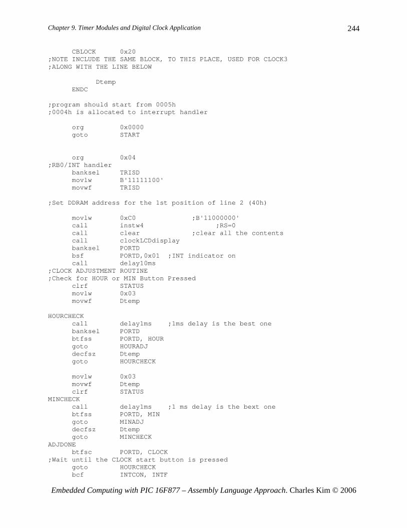
CBLOCK 0x20;NOTE INCLUDE THE SAME BLOCK, TO THIS PLACE, USED FOR CLOCK3;ALONG WITH THE LINE BELOW
DtempENDC
;program should start from 0005h;0004h is allocated to interrupt handler
org 0x0000goto START
org 0x04;RB0/INT handler
banksel TRISDmovlw B'11111100'movwf TRISD
;Set DDRAM address for the 1st position of line 2 (40h)
movlw 0xC0 ;B'11000000'call instw4 ;RS=0call clear ;clear all the contentscall clockLCDdisplaybanksel PORTDbsf PORTD,0x01 ;INT indicator oncall delay10ms
;CLOCK ADJUSTMENT ROUTINE;Check for HOUR or MIN Button Pressed
clrf STATUSmovlw 0x03movwf Dtemp
HOURCHECKcall delay1ms ;1ms delay is the best onebanksel PORTDbtfss PORTD, HOURgoto HOURADJdecfsz Dtempgoto HOURCHECK
movlw 0x03movwf Dtempclrf STATUS
MINCHECKcall delay1ms ;1 ms delay is the bext onebtfss PORTD, MINgoto MINADJdecfsz Dtempgoto MINCHECK
ADJDONEbtfsc PORTD, CLOCK
;Wait until the CLOCK start button is pressedgoto HOURCHECKbcf INTCON, INTF
Chapter 9. Timer Modules and Digital Clock Application
Embedded Computing with PIC 16F877 – Assembly Language Approach. Charles Kim © 2006
245
banksel PORTDbcf PORTD, 0x01 ;INT indicator offretfie ;return to main program
;hour adjustmentHOURADJ
clrf STATUSbanksel HHincf HHmovf HH,0xorlw B'00011000' ;24=00011000btfsc STATUS,ZEROclrf HH
;IF HH=24 set to 0;
goto prep
MINADJclrf STATUSbanksel MMincf MM
;IF MM=60 set to 0movf MM,0xorlw B'00111100' ;60=00111100btfsc STATUS,ZEROclrf MMgoto prep
prepbanksel HHmovf HH,0movwf hmscall h2d2movf hms1dec,0movwf hh1decmovf hms0dec,0movwf hh0dec
movf MM,0movwf hmscall h2d2movf hms1dec,0movwf mm1decmovf hms0dec,0movwf mm0dec
movlw 0x00 ;for SSmovwf ss1decmovwf ss0dec
;Set DDRAM address for the 1st position of line 2 (40h)movlw 0xC0 ;B'11000000'call instw4 ;RS=0call clockLCDdisplaycall delay10msgoto ADJDONE
; END of INT handler
Chapter 9. Timer Modules and Digital Clock Application
Embedded Computing with PIC 16F877 – Assembly Language Approach. Charles Kim © 2006
246
StartBANKSEL TRISB
; 1 for input, 0 for output
movlw 0x01movwf TRISB ;All output except RB0/INT
banksel TRISDmovlw B'11111100' ;PORTD all inputs except the last twomovwf TRISD
banksel PORTDbcf PORTD,0x01bcf PORTD, 0x00 ;OFf the LEDs
;LCD routine startscall delay10mscall delay10ms
banksel PORTBbcf PORTB, RW ;RW set LOW here
;give LCD module to reset automatically
;For RB0/INTbanksel INTCONclrf INTCON ;int disabledbsf INTCON, GIE ;interrupt enabledbsf INTCON, INTE ;RB0/INT enable
;FOR TMR0clrf TMR0movlw 0xC7banksel OPTION_REG ;pre-scaler at 255movwf OPTION_REG ;10000111 (with INTEDG=0)banksel TMR0clrf TMR0
;END FOR TMR0
;THE ONLY CHANGE IN 4-BIT INTERFACING;EXCEPT 2 SUBROUTINES;;Function for 4-bit (only one write must be done);In other words, send only the high nibble;IMPORTANTLCDINIT
movlw 0x28call hnibble4
;Fundtion for 4-bit, 2-line display, and 5x8 dot matrixmovlw 0x28call instw4
;Display On, CUrsor On, No blinkingmovlw 0x0E ;0F would blink
Chapter 9. Timer Modules and Digital Clock Application
Embedded Computing with PIC 16F877 – Assembly Language Approach. Charles Kim © 2006
247
call instw4;DDRAM address increment by one & cursor shift to right
movlw 0x06call instw4
LCDREADY;DISPLAY CLEAR
movlw 0x01call instw4
;Set DDRAM ADDRESmovlw 0x80 ;00call instw4
;WRITE DATA in the 1st position of line 1movlw 0x50 ;Pcall dataw4
movlw 0x49 ;Icall dataw4
movlw 0x43 ;Ccall dataw4movlw ' 'call dataw4movlw 'C'call dataw4movlw 'L'call dataw4movlw 'O'call ataw4movlw 'C'call dataw4movlw 'K'call dataw4
;call clear
AGAIN;CLOCK DISPLAY;Set DDRAM address for the 1st position of line 2 (40h)
movlw 0xC0 ;B'11000000'call instw4 ;RS=0
;CLOCK DISPLAY PART
movf SS,0movwf hmscall h2d2movf hms1dec,0movwf ss1decmovf hms0dec,0movwf ss0dec
movf MM,0movwf hms
Chapter 9. Timer Modules and Digital Clock Application
Embedded Computing with PIC 16F877 – Assembly Language Approach. Charles Kim © 2006
248
call h2d2movf hms1dec,0movwf mm1decmovf hms0dec,0movwf mm0dec
movf HH,0movwf hmscall h2d2movf hms1dec,0movwf hh1decmovf hms0dec,0movwf hh0dec
call clockLCDdisplaycall delay1sincf SSmovf SS,0clrf STATUSxorlw B'00111100' ;if SS=60(d) or 3C or 0011 1100btfss STATUS, ZEROgoto again
clrf SSincf MMmovf MM,0clrf STATUSxorlw B'00111100'btfss STATUS,ZEROgoto again
clrf MMincf HHmovf HH,0clrf STATUS
;check 24hour 24d = 00011000xorlw B'00011000'btfss STATUS,ZEROgoto againclrf STATUScall cleargoto again
;SUBROUTINES;HERE
END;end of program
When you compile the full code and run it, the first LCD display would be like this: the clock starts from 00:00:00.
Chapter 9. Timer Modules and Digital Clock Application
Embedded Computing with PIC 16F877 – Assembly Language Approach. Charles Kim © 2006
249
When you press the TIME button, the LCD would go back to 00:00:00. And the clock does not tick, instead, it waits for HOUR, MIN, or CLOCK button.
If you press the buttons of HOUR and MIN, the numbers for HH and MM would increase.
When you finally press the CLOCK button, the digital clock starts to tick from the set time. If you leave your clock run for a day or so, you may notice that your clock is slightly slower than your watch. The reason is that LCD display consumes a lot of time, a few tens of milli-seconds. Therefore, to make your digital clock reasonably accurate, we reduce down the number of overflows (remember 76) to make an exact 1 second delay. It is very hard to consider all the delay factors in the program and find the exact number of the overflow count, however, just one or two trial and error hopefully gives us the best number. So we change the 1 second time delay to accommodate the delay involved in LCD display, as follows. ;DELAY SUBROUTINE for 1 Second delay;DELAY1s
banksel countmovlw 0x3C ;Count=76 for 1 second to expire
;lowered to 60 to;accommodate LCD delays
movwf count
over btfss INTCON, T0IF ;Tmr0 overflow?goto overbcf INTCON, T0IF ;resetdecfsz countgoto over
return
Chapter 9. Timer Modules and Digital Clock Application
Embedded Computing with PIC 16F877 – Assembly Language Approach. Charles Kim © 2006
250
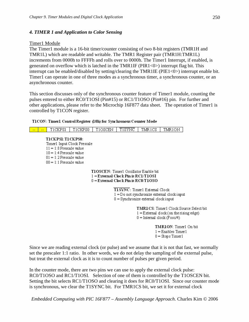
4. TIMER 1 and Application to Color Sensing Timer1 Module The Timer1 module is a 16-bit timer/counter consisting of two 8-bit registers (TMR1H and TMR1L) which are readable and writable. The TMR1 Register pair (TMR1H:TMR1L) increments from 0000h to FFFFh and rolls over to 0000h. The Timer1 Interrupt, if enabled, is generated on overflow which is latched in the TMR1IF (PIR1<0>) interrupt flag bit. This interrupt can be enabled/disabled by setting/clearing the TMR1IE (PIE1<0>) interrupt enable bit. Timer1 can operate in one of three modes as a synchronous timer, a synchronous counter, or an asynchronous counter. This section discusses only of the synchronous counter feature of Timer1 module, counting the pulses entered to either RC0/T1OSI (Pin#15) or RC1/T1OSO (Pin#16) pin. For further and other applications, please refer to the Microchip 16F877 data sheet. The operation of Timer1 is controlled by T1CON register.
Since we are reading external clock (or pulse) and we assume that it is not that fast, we normally set the prescaler 1:1 ratio. In other words, we do not delay the sampling of the external pulse, but treat the external clock as it is to count number of pulses per given period. In the counter mode, there are two pins we can use to apply the external clock pulse: RC0/T1OSO and RC1/T1OSI. Selection of one of them is controlled by the T1OSCEN bit. Setting the bit selects RC1/T1OSO and clearing it does for RC0/T1OSI. Since our counter mode is synchronous, we clear the T1SYNC bit. For TMR1CS bit, we set it for external clock
Chapter 9. Timer Modules and Digital Clock Application
Embedded Computing with PIC 16F877 – Assembly Language Approach. Charles Kim © 2006
251
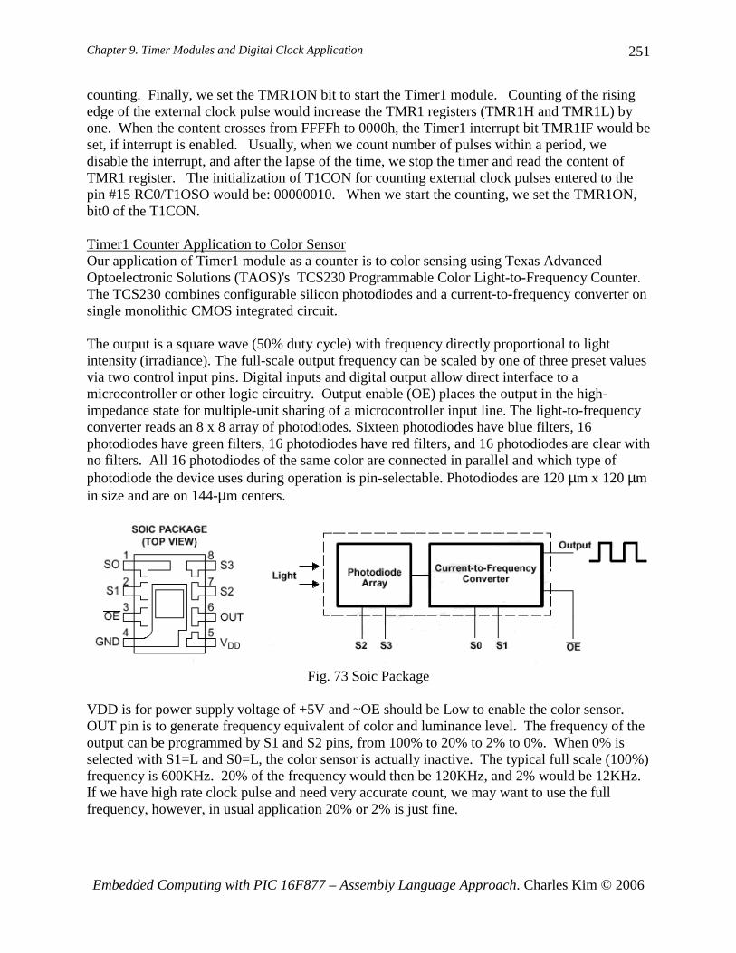
counting. Finally, we set the TMR1ON bit to start the Timer1 module. Counting of the rising edge of the external clock pulse would increase the TMR1 registers (TMR1H and TMR1L) by one. When the content crosses from FFFFh to 0000h, the Timer1 interrupt bit TMR1IF would be set, if interrupt is enabled. Usually, when we count number of pulses within a period, we disable the interrupt, and after the lapse of the time, we stop the timer and read the content of TMR1 register. The initialization of T1CON for counting external clock pulses entered to the pin #15 RC0/T1OSO would be: 00000010. When we start the counting, we set the TMR1ON, bit0 of the T1CON. Timer1 Counter Application to Color Sensor Our application of Timer1 module as a counter is to color sensing using Texas Advanced Optoelectronic Solutions (TAOS)'s TCS230 Programmable Color Light-to-Frequency Counter. The TCS230 combines configurable silicon photodiodes and a current-to-frequency converter on single monolithic CMOS integrated circuit. The output is a square wave (50% duty cycle) with frequency directly proportional to light intensity (irradiance). The full-scale output frequency can be scaled by one of three preset values via two control input pins. Digital inputs and digital output allow direct interface to a microcontroller or other logic circuitry. Output enable (OE) places the output in the high-impedance state for multiple-unit sharing of a microcontroller input line. The light-to-frequency converter reads an 8 x 8 array of photodiodes. Sixteen photodiodes have blue filters, 16 photodiodes have green filters, 16 photodiodes have red filters, and 16 photodiodes are clear with no filters. All 16 photodiodes of the same color are connected in parallel and which type of photodiode the device uses during operation is pin-selectable. Photodiodes are 120 µm x 120 µm in size and are on 144-µm centers.
Fig. 73 Soic Package
VDD is for power supply voltage of +5V and ~OE should be Low to enable the color sensor. OUT pin is to generate frequency equivalent of color and luminance level. The frequency of the output can be programmed by S1 and S2 pins, from 100% to 20% to 2% to 0%. When 0% is selected with S1=L and S0=L, the color sensor is actually inactive. The typical full scale (100%) frequency is 600KHz. 20% of the frequency would then be 120KHz, and 2% would be 12KHz. If we have high rate clock pulse and need very accurate count, we may want to use the full frequency, however, in usual application 20% or 2% is just fine.
Chapter 9. Timer Modules and Digital Clock Application
Embedded Computing with PIC 16F877 – Assembly Language Approach. Charles Kim © 2006
252
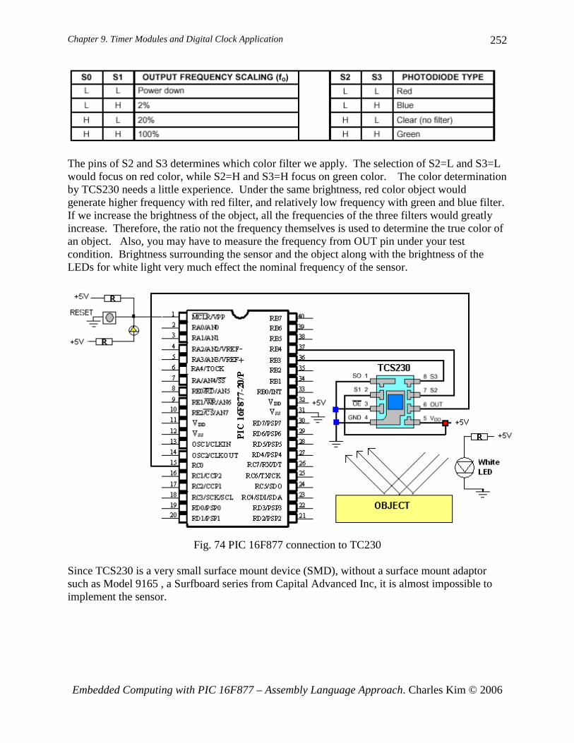
The pins of S2 and S3 determines which color filter we apply. The selection of S2=L and S3=L would focus on red color, while S2=H and S3=H focus on green color. The color determination by TCS230 needs a little experience. Under the same brightness, red color object would generate higher frequency with red filter, and relatively low frequency with green and blue filter. If we increase the brightness of the object, all the frequencies of the three filters would greatly increase. Therefore, the ratio not the frequency themselves is used to determine the true color of an object. Also, you may have to measure the frequency from OUT pin under your test condition. Brightness surrounding the sensor and the object along with the brightness of the LEDs for white light very much effect the nominal frequency of the sensor.
Fig. 74 PIC 16F877 connection to TC230
Since TCS230 is a very small surface mount device (SMD), without a surface mount adaptor such as Model 9165 , a Surfboard series from Capital Advanced Inc, it is almost impossible to implement the sensor.
Chapter 9. Timer Modules and Digital Clock Application
Embedded Computing with PIC 16F877 – Assembly Language Approach. Charles Kim © 2006
253
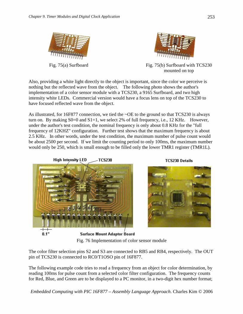
Fig. 75(a) Surfboard Fig. 75(b) Surfboard with TCS230
mounted on top Also, providing a white light directly to the object is important, since the color we perceive is nothing but the reflected wave from the object. The following photo shows the author's implementation of a color sensor module with a TCS230, a 9165 Surfboard, and two high intensity white LEDs. Commercial version would have a focus lens on top of the TCS230 to have focused reflected wave from the object. As illustrated, for 16F877 connection, we tied the ~OE to the ground so that TCS230 is always turn on. By making S0=0 and S1=1, we select 2% of full frequency, i.e., 12 KHz. However, under the author's test condition, the nominal frequency is only about 0.8 KHz for the "full frequency of 12KHZ" configuration. Further test shows that the maximum frequency is about 2.5 KHz. In other words, under the test condition, the maximum number of pulse count would be about 2500 per second. If we limit the counting period to only 100ms, the maximum number would only be 250, which is small enough to be filled only the lower TMR1 register (TMR1L).
Fig. 76 Implementation of color sensor module
The color filter selection pins S2 and S3 are connected to RB5 and RB4, respectively. The OUT pin of TCS230 is connected to RC0/T1OSO pin of 16F877. The following example code tries to read a frequency from an object for color determination, by reading 100ms for pulse count from a selected color filter configuration. The frequency counts for Red, Blue, and Green are to be displayed to a PC monitor, in a two-digit hex number format;
Chapter 9. Timer Modules and Digital Clock Application
Embedded Computing with PIC 16F877 – Assembly Language Approach. Charles Kim © 2006
254
Red1 & Red0, Blue1 & Blue0, and Green1 & Green0. The code does not try to determine the color, instead it just spews out the R, G, B, ratios in frequency counts. The color determination is left to the readers. The listing omits the subroutines, as usual. The readers are encouraged to carefully follow the comments in the following code for better understanding of the program. Note that the delay1s subroutine used here does not utilize the Timer0 module; instead this is the first time delay subroutine we made using just numbers of instructions to make 1 second delay. To ease confusion, only delay1s subroutine is included in the subroutine section. All others are omitted. ;TCS230.asm;; This is to count 50% duty cycle pulses from TCS230 color sensor; using tmr1 module; of synchronous counter feature;; Output pulse from TCS230 is connected to RC0 (TICK1); Color Filter Selection S2 and S3 are connected to RB5 and RB4 respectively; S2 (RB5) S3 (RB4); L L Red Filter; L H Blue Filter; H H Green Filter; H L No Filter (Clear); Output Pulse Frequency Selection S0 and S1 are as follows (for 12 KHznominal); S0 S1; L H (12 KHz)---actual value is much smaller in a test condition; like 1 – 2KHz;
list P = 16F877
STATUS EQU 0x03PORTB EQU 0x06TRISB EQU 0x86PIE1 EQU 0x8CPIR1 EQU 0x0CT1CON EQU 0x10TMR1L EQU 0x0ETMR1H EQU 0x0FINTCON EQU 0x8BTMR1ON EQU 0x00S2 EQU 0x05S3 EQU 0x04ZERO EQU 0x02 ;Z flagTXSTA EQU 0x98 ;TX status and controlRCSTA EQU 0x18 ;RX status and controlSPBRG EQU 0x99 ;Baud Rate assignmentTXREG EQU 0x19 ;USART TX RegisterRCREG EQU 0x1A ;USART RX RegisterPIR1 EQU 0x0C ;USART RX/TX buffer status (empty or full)RCIF EQU 0x05 ;PIR1<5>: RX Buffer 1-Full 0-EmptyTXIF EQU 0x04 ;PIR1<4>: TX Buffer 1-empty 0-fullTXMODE EQU 0x20 ;TXSTA=00100000 : 8-bit, AsyncRXMODE EQU 0x90 ;RCSTA=10010000 : 8-bit, enable port, enable RX
Chapter 9. Timer Modules and Digital Clock Application
Embedded Computing with PIC 16F877 – Assembly Language Approach. Charles Kim © 2006
255
BAUD EQU 0x0F ;0x0F (19200), 0x1F (9600)
;;RAM
CBLOCK 0x20TEMPRedTEMPBlueTEMPGreenTEMPRed1Red0Blue1Blue0Green1Green0ASCIIregKount120us ;Delay count (number of instr cycles for delay)Kount100usKount1msKount10msKount100msKount1sKount10sKount1m
ENDC
;;=========================================================
org 0x0000GOTO START
;=========== ===========================================org 0x05
STARTcall Async_mode
BANKSEL TRISBmovlw B'11000000'movwf TRISB ;PORTB setting for S2 and S3
;TMR1 Initializationbanksel T1CONclrf T1CON
banksel INTCONclrf INTCON ;Disable interrupt
banksel PIE1clrf PIE1 ;disable peripheral interrupt
banksel PIR1clrf PIR1 ;clear peripheral interrupt flag
banksel T1CON
Chapter 9. Timer Modules and Digital Clock Application
Embedded Computing with PIC 16F877 – Assembly Language Approach. Charles Kim © 2006
256
movlw '00000010'movwf T1CON ;1:1 prescaler
;External Clock Source at RC0/T1OSO (pin #15)
;TMR1 is OFF now
AGAINbanksel PORTBbcf PORTB, S2bcf PORTB, S3 ;RED filter is setcall delay10ms ;Wait for the setting is donebanksel TMR1Hclrf TMR1Hclrf TMR1L ;Clear the counting regsiterbsf T1CON, TMR1ON ;Tmr1 now starts to incrementcall delay100ms ;Continue counting for 100msbanksel T1CONbcf T1CON, TMR1ON ;TMR1 is OFFbanksel TMR1H
; movf TMR1H,0; movwf T1HIGH
movf TMR1L,0 ;Get the RED count to Wmovwf RedTEMP ;Store the RED count to RedTEMP register
; RED is finished;
call delay10ms ;A short delay before Blue reading; Go for Blue
banksel PORTBbcf PORTB, S2bsf PORTB, S3call delay10msbanksel TMR1Hclrf TMR1Hclrf TMR1Lbsf T1CON, TMR1ON ;Tmr1 now starts to incrementcall delay100ms ;for 100ms
banksel T1CON
bcf T1CON, TMR1ON ;TMR1 is OFF
banksel TMR1H; movf TMR1H,0; movwf T1HIGH
movf TMR1L,0movwf BlueTEMP ;Blue count
;call delay10ms
; Go for Greenbanksel PORTBbsf PORTB, S2bsf PORTB, S3call delay10msbanksel TMR1Hclrf TMR1Hclrf TMR1Lbsf T1CON, TMR1ON ;Tmr1 now starts to increment
Chapter 9. Timer Modules and Digital Clock Application
Embedded Computing with PIC 16F877 – Assembly Language Approach. Charles Kim © 2006
257
call delay100ms ;for 100ms
banksel T1CON
bcf T1CON, TMR1ON ;TMR1 is OFF
banksel TMR1H; movf TMR1H,0; movwf T1HIGH
movf TMR1L,0movwf GreenTEMP ;Green pulse count
;Display Preparation
;REDmovf RedTEMP,0movwf TEMPswapf TEMP,0 ;SWAP upper and lower nibbles --->Wandlw 0x0F ;Mask off upper nibble
call HTOAmovwf Red1
movf RedTEMP,0andlw 0x0F ;mask of upper nibblecall HTOAmovwf Red0
;Bluemovf BlueTEMP,0movwf TEMPswapf TEMP,0 ;SWAP upper and lower nibbles --->Wandlw 0x0F ;Mask off upper nibble
call HTOAmovwf Blue1
movf BlueTEMP,0andlw 0x0F ;mask of upper nibblecall HTOAmovwf Blue0
;Greenmovf GreenTEMP,0movwf TEMPswapf TEMP,0 ;SWAP upper and lower nibbles --->W
andlw 0x0F ;Mask off upper nibble
call HTOAmovwf Green1
movf GreenTEMP,0andlw 0x0F ;mask of upper nibblecall HTOA
Chapter 9. Timer Modules and Digital Clock Application
Embedded Computing with PIC 16F877 – Assembly Language Approach. Charles Kim © 2006
258
movwf Green0
;display;RED
movlw 'R'call TXPOLLmovlw ':'call TXPOLLmovf Red1,0call TXPOLLmovf Red0,0call TXPOLLmovlw ' 'call TXPOLL
;BLUEmovlw 'B'call TXPOLLmovlw ':'call TXPOLLmovf Blue1,0call TXPOLLmovf Blue0,0call TXPOLLmovlw ' 'call TXPOLL
;GREENmovlw 'G'call TXPOLLmovlw ':'call TXPOLLmovf Green1,0call TXPOLLmovf Green0,0call TXPOLLmovlw ' 'call TXPOLLcall CRLF
call delay1s ;1 sec delay after R, G, B readingsgoto AGAIN
;SUBROUTINE SECTION;1 sec delay;call 100 times of 10ms delayDelay1s
banksel Kount1smovlw H'64'movwf Kount1s
R1s call Delay10msdecfsz Kount1sgoto R1sreturn
;;INCLUDE OTHER SUBROUTINES
Chapter 9. Timer Modules and Digital Clock Application
Embedded Computing with PIC 16F877 – Assembly Language Approach. Charles Kim © 2006
259
; HERE;
END;end of program
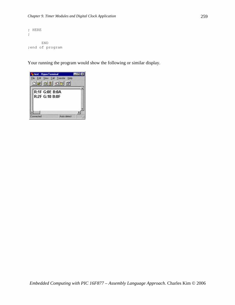
Your running the program would show the following or similar display.


