Embed Size (px)
Citation preview
Directorate of Technical Education Karnataka State 15EC52T Page 1
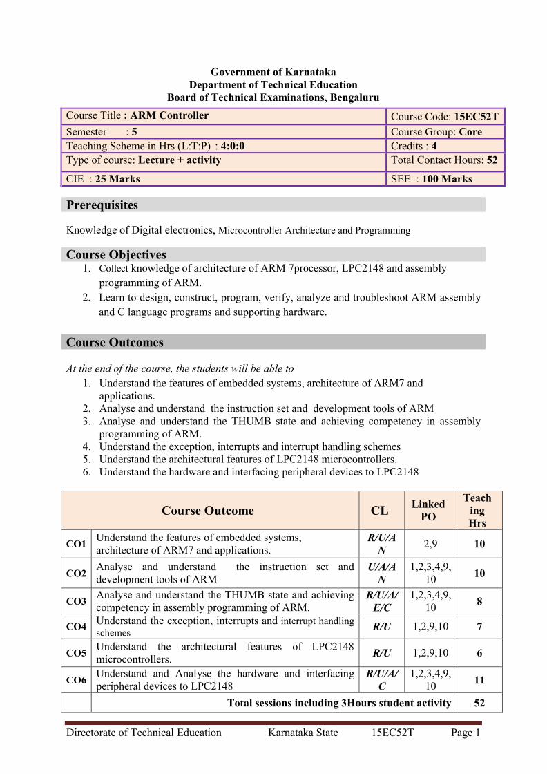
Government of KarnatakaDepartment of Technical Education
Board of Technical Examinations, Bengaluru
Prerequisites
Knowledge of Digital electronics, Microcontroller Architecture and Programming
Course Objectives1. Collect knowledge of architecture of ARM 7processor, LPC2148 and assembly
programming of ARM.2. Learn to design, construct, program, verify, analyze and troubleshoot ARM assembly
and C language programs and supporting hardware.
Course Outcomes
At the end of the course, the students will be able to1. Understand the features of embedded systems, architecture of ARM7 and
applications.2. Analyse and understand the instruction set and development tools of ARM3. Analyse and understand the THUMB state and achieving competency in assembly
programming of ARM.4. Understand the exception, interrupts and interrupt handling schemes5. Understand the architectural features of LPC2148 microcontrollers.6. Understand the hardware and interfacing peripheral devices to LPC2148
Course Outcome CL Linked PO
Teaching Hrs
CO1Understand the features of embedded systems, architecture of ARM7 and applications.
R/U/AN
2,9 10
CO2Analyse and understand the instruction set and development tools of ARM
U/A/AN
1,2,3,4,9,10 10
CO3Analyse and understand the THUMB state and achieving competency in assembly programming of ARM.
R/U/A/E/C
1,2,3,4,9,10
8
CO4Understand the exception, interrupts and interrupt handling schemes
R/U 1,2,9,10 7
CO5Understand the architectural features of LPC2148 microcontrollers.
R/U 1,2,9,10 6
CO6Understand and Analyse the hardware and interfacing peripheral devices to LPC2148
R/U/A/C
1,2,3,4,9,10 11
Total sessions including 3Hours student activity 52
Course Title : ARM Controller Course Code: 15EC52TSemester : 5 Course Group: CoreTeaching Scheme in Hrs (L:T:P) : 4:0:0 Credits : 4 Type of course: Lecture + activity Total Contact Hours: 52
CIE : 25 Marks SEE : 100 Marks
Directorate of Technical Education Karnataka State 15EC52T Page 2
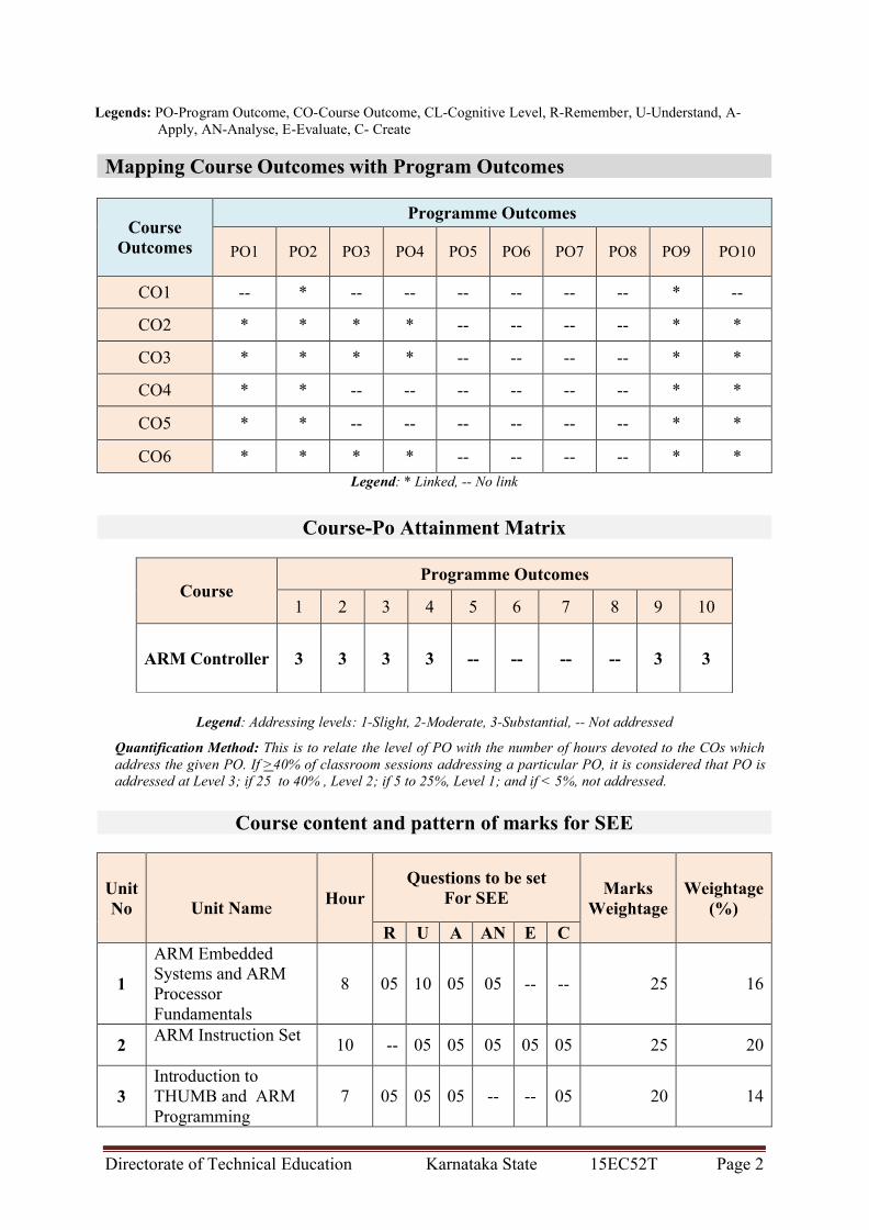
Legends: PO-Program Outcome, CO-Course Outcome, CL-Cognitive Level, R-Remember, U-Understand, A-Apply, AN-Analyse, E-Evaluate, C- Create
Mapping Course Outcomes with Program Outcomes
Course Outcomes
Programme Outcomes
PO1 PO2 PO3 PO4 PO5 PO6 PO7 PO8 PO9 PO10
CO1 -- * -- -- -- -- -- -- * --
CO2 * * * * -- -- -- -- * *
CO3 * * * * -- -- -- -- * *
CO4 * * -- -- -- -- -- -- * *
CO5 * * -- -- -- -- -- -- * *
CO6 * * * * -- -- -- -- * *Legend: * Linked, -- No link
Course-Po Attainment Matrix
Legend: Addressing levels: 1-Slight, 2-Moderate, 3-Substantial, -- Not addressed
Quantification Method: This is to relate the level of PO with the number of hours devoted to the COs which address the given PO. If >40% of classroom sessions addressing a particular PO, it is considered that PO is addressed at Level 3; if 25 to 40% , Level 2; if 5 to 25%, Level 1; and if < 5%, not addressed.
Course content and pattern of marks for SEE
UnitNo Unit Name
HourQuestions to be set
For SEE MarksWeightage
Weightage(%)
R U A AN E C
1
ARM Embedded Systems and ARM Processor Fundamentals
8 05 10 05 05 -- -- 25 16
2ARM Instruction Set
10 -- 05 05 05 05 05 25 20
3Introduction to THUMB and ARM Programming
7 05 05 05 -- -- 05 20 14
CourseProgramme Outcomes
1 2 3 4 5 6 7 8 9 10
ARM Controller 3 3 3 3 -- -- -- -- 3 3
Directorate of Technical Education Karnataka State 15EC52T Page 3
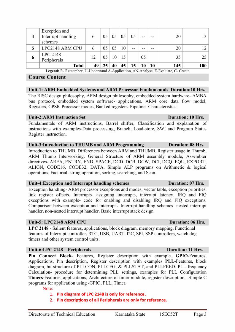
4Exception and Interrupt handling schemes
6 05 05 05 05 -- -- 20 13
5 LPC2148 ARM CPU 6 05 05 10 -- -- -- 20 12
6LPC 2148 –Peripherals
12 05 10 15 05 35 25
Total 49 25 40 45 15 10 10 145 100Legend: R- Remember, U-Understand A-Application, AN-Analyse, E-Evaluate, C- Create
Course Content
Unit-1: ARM Embedded Systems and ARM Processor Fundamentals Duration:10 Hrs.The RISC design philosophy, ARM design philosophy, embedded system hardware- AMBA bus protocol, embedded system software- applications. ARM core data flow model, Registers, CPSR-Processor modes, Banked registers. Pipeline- Characteristics.
Unit-2:ARM Instruction Set Duration: 10 Hrs.Fundamentals of ARM instructions, Barrel shifter, Classification and explanation of instructions with examples-Data processing, Branch, Load-store, SWI and Program Status Register instruction.
Unit-3:Introduction to THUMB and ARM Programming Duration: 08 Hrs.Introduction to THUMB, Differences between ARM and THUMB, Register usage in Thumb, ARM Thumb Interworking. General Structure of ARM assembly module, Assembler directives- AREA, ENTRY, END, SPACE, DCD, DCB, DCW, DCI, DCQ, EQU, EXPORT,ALIGN, CODE16, CODE32, DATA. Simple ALP programs on Arithmetic & logical operations, Factorial, string operation, sorting, searching, and Scan.
Unit-4:Exception and Interrupt handling schemes Duration: 07 Hrs.Exception handling- ARM processor exceptions and modes, vector table, exception priorities, link register offsets. Interrupts- assigning interrupts, interrupt latency, IRQ and FIQ exceptions with example- code for enabling and disabling IRQ and FIQ exceptions, Comparison between exception and interrupts. Interrupt handling schemes- nested interrupt handler, non-nested interrupt handler. Basic interrupt stack design.
Unit-5: LPC2148 ARM CPU Duration: 06 Hrs.LPC 2148 - Salient features, applications, block diagram, memory mapping. Functional features of Interrupt controller, RTC, USB, UART, I2C, SPI, SSP controllers, watch dog timers and other system control units.
Unit-6:LPC 2148 – Peripherals Duration: 11 Hrs.Pin Connect Block- Features, Register description with example. GPIO-Features, Applications, Pin description, Register description with examples PLL-Features, block diagram, bit structure of PLLCON, PLLCFG, & PLLSTAT, and PLLFEED. PLL frequency Calculation- procedure for determining PLL settings, examples for PLL Configuration Timers-Features, applications, Architecture of timer module, register description, Simple C programs for application using -GPIO, PLL, Timer.
Note:1. Pin diagram of LPC 2148 is only for reference.2. Pin descriptions of all Peripherals are only for reference.
Directorate of Technical Education Karnataka State 15EC52T Page 4
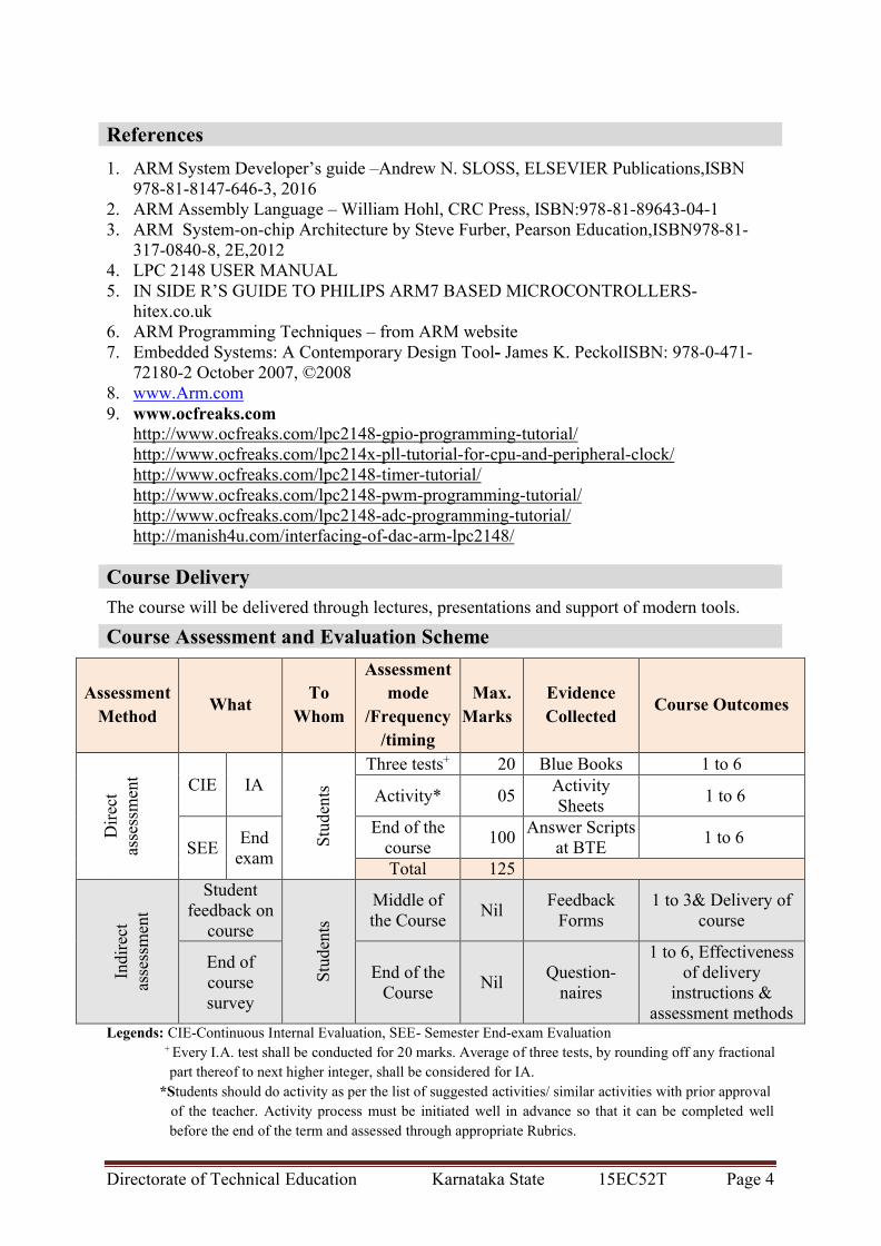
References
1. ARM System Developer’s guide –Andrew N. SLOSS, ELSEVIER Publications,ISBN 978-81-8147-646-3, 2016
2. ARM Assembly Language – William Hohl, CRC Press, ISBN:978-81-89643-04-1 3. ARM System-on-chip Architecture by Steve Furber, Pearson Education,ISBN978-81-
317-0840-8, 2E,20124. LPC 2148 USER MANUAL 5. IN SIDE R’S GUIDE TO PHILIPS ARM7 BASED MICROCONTROLLERS-
hitex.co.uk6. ARM Programming Techniques – from ARM website7. Embedded Systems: A Contemporary Design Tool- James K. PeckolISBN: 978-0-471-
72180-2 October 2007, ©20088. www.Arm.com9. www.ocfreaks.com
http://www.ocfreaks.com/lpc2148-gpio-programming-tutorial/http://www.ocfreaks.com/lpc214x-pll-tutorial-for-cpu-and-peripheral-clock/http://www.ocfreaks.com/lpc2148-timer-tutorial/http://www.ocfreaks.com/lpc2148-pwm-programming-tutorial/http://www.ocfreaks.com/lpc2148-adc-programming-tutorial/http://manish4u.com/interfacing-of-dac-arm-lpc2148/
Course Delivery
The course will be delivered through lectures, presentations and support of modern tools.
Course Assessment and Evaluation Scheme
AssessmentMethod
WhatTo
Whom
Assessment mode
/Frequency/timing
Max. Marks
Evidence Collected
Course Outcomes
CIE IAThree tests+ 20 Blue Books 1 to 6
Activity* 05Activity Sheets
1 to 6
SEEEnd
exam
End of the course
100Answer Scripts
at BTE1 to 6
Total 125Student
feedback on course
Middle of the Course
NilFeedback
Forms1 to 3& Delivery of
course
End of course survey
End of the Course
NilQuestion-
naires
1 to 6, Effectiveness of delivery
instructions & assessment methods
Legends: CIE-Continuous Internal Evaluation, SEE- Semester End-exam Evaluation+ Every I.A. test shall be conducted for 20 marks. Average of three tests, by rounding off any fractional part thereof to next higher integer, shall be considered for IA.
*Students should do activity as per the list of suggested activities/ similar activities with prior approvalof the teacher. Activity process must be initiated well in advance so that it can be completed well before the end of the term and assessed through appropriate Rubrics.
Directorate of Technical Education Karnataka State 15EC52T Page 5
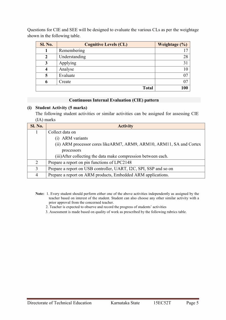
Questions for CIE and SEE will be designed to evaluate the various CLs as per the weightage shown in the following table.
Sl. No. Cognitive Levels (CL) Weightage (%)1 Remembering 172 Understanding 28
3 Applying 314 Analyse 10
5 Evaluate 076 Create 07
Total 100
Continuous Internal Evaluation (CIE) pattern
(i) Student Activity (5 marks)The following student activities or similar activities can be assigned for assessing CIE (IA) marks
Sl. No. Activity1 Collect data on
(i) ARM variants (ii) ARM processor cores likeARM7, ARM9, ARM10, ARM11, SA and Cortex
processors(iii)After collecting the data make compression between each.
2 Prepare a report on pin functions of LPC21483 Prepare a report on USB controller, UART, I2C, SPI, SSP and so on4 Prepare a report on ARM products, Embedded ARM applications.
Note: 1. Every student should perform either one of the above activities independently as assigned by the teacher based on interest of the student. Student can also choose any other similar activity with a prior approval from the concerned teacher.
2. Teacher is expected to observe and record the progress of students’ activities3. Assessment is made based on quality of work as prescribed by the following rubrics table.
Directorate of Technical Education Karnataka State 15EC52T Page 6
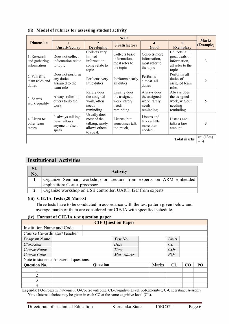
(ii) Model of rubrics for assessing student activity
Sl. No.
Activity
1 Organize Seminar, workshop or Lecture from experts on ARM embedded application/ Cortex processor
2 Organize workshop on USB controller, UART, I2C from experts
(iii) CIE/IA Tests (20 Marks)Three tests have to be conducted in accordance with the test pattern given below and average marks of them are considered for CIE/IA with specified schedule.
(iv) Format of CIE/IA test question paperCIE Question Paper
Institution Name and CodeCourse Co-ordinator/TeacherProgram Name Test No. UnitsClass/Sem Date CLCourse Name Time COsCourse Code Max. Marks POsNote to students: Answer all questionsQuestion No. Question Marks CL CO PO
1234
Legends: PO-Program Outcome, CO-Course outcome, CL-Cognitive Level, R-Remember, U-Understand, A-ApplyNote: Internal choice may be given in each CO at the same cognitive level (CL).
DimensionScale
Marks(Example)1
Unsatisfactory2
Developing3 Satisfactory
4Good
5Exemplary
1. Research and gathering information
Does not collect information relate to topic
Collects very limited information, some relate to topic
Collects basic information,most refer to the topic
Collects more information, most refer to the topic
Collects a great deals of information, all refer to the topic
3
2. Full-fills team roles and duties
Does not perform any duties assigned to the team role
Performs very little duties
Performs nearly all duties
Performs almost all duties
Performs all duties of assigned team roles
2
3. Shares work equality
Always relies on others to do the work
Rarely does the assigned work, often needs reminding
Usually does the assigned work, rarely needs reminding
Always does the assigned work, rarely needs reminding.
Always does the assigned work, without needing reminding
5
4. Listen to other team mates
Is always talking, never allows anyone to else to speak
Usually does most of the talking, rarely allows others to speak
Listens, but sometimes talk too much,
Listens and talks a little more than needed.
Listens and talks a fare amount
3
Total marksceil(13/4)= 4
Institutional Activities
Directorate of Technical Education Karnataka State 15EC52T Page 7
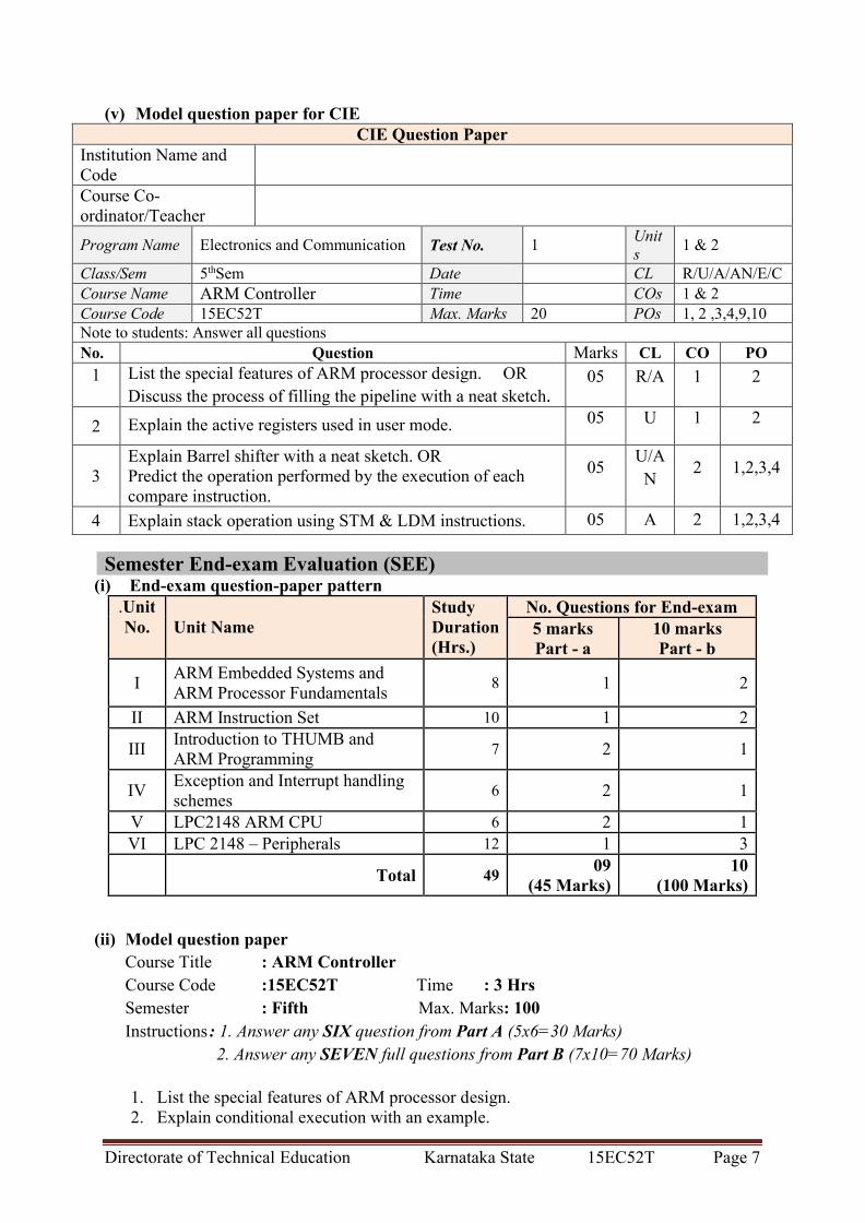
(v) Model question paper for CIECIE Question Paper
Institution Name and CodeCourse Co-ordinator/Teacher
Program Name Electronics and Communication Test No. 1Units
1 & 2
Class/Sem 5thSem Date CL R/U/A/AN/E/CCourse Name ARM Controller Time COs 1 & 2Course Code 15EC52T Max. Marks 20 POs 1, 2 ,3,4,9,10Note to students: Answer all questionsNo. Question Marks CL CO PO
1 List the special features of ARM processor design. ORDiscuss the process of filling the pipeline with a neat sketch.
05 R/A 1 2
2 Explain the active registers used in user mode. 05 U 1 2
3Explain Barrel shifter with a neat sketch. ORPredict the operation performed by the execution of each compare instruction.
05U/AN
2 1,2,3,4
4 Explain stack operation using STM & LDM instructions. 05 A 2 1,2,3,4
Semester End-exam Evaluation (SEE)(i) End-exam question-paper pattern
.UnitNo. Unit Name
StudyDuration(Hrs.)
No. Questions for End-exam5 marksPart - a
10 marksPart - b
IARM Embedded Systems andARM Processor Fundamentals
8 1 2
II ARM Instruction Set 10 1 2
IIIIntroduction to THUMB and ARM Programming
7 2 1
IVException and Interrupt handling schemes
6 2 1
V LPC2148 ARM CPU 6 2 1VI LPC 2148 – Peripherals 12 1 3
Total 4909
(45 Marks)10
(100 Marks)
(ii) Model question paperCourse Title : ARM Controller Course Code :15EC52T Time : 3 HrsSemester : Fifth Max. Marks: 100Instructions: 1. Answer any SIX question from Part A (5x6=30 Marks)
2. Answer any SEVEN full questions from Part B (7x10=70 Marks)
1. List the special features of ARM processor design. 2. Explain conditional execution with an example.
Directorate of Technical Education Karnataka State 15EC52T Page 8
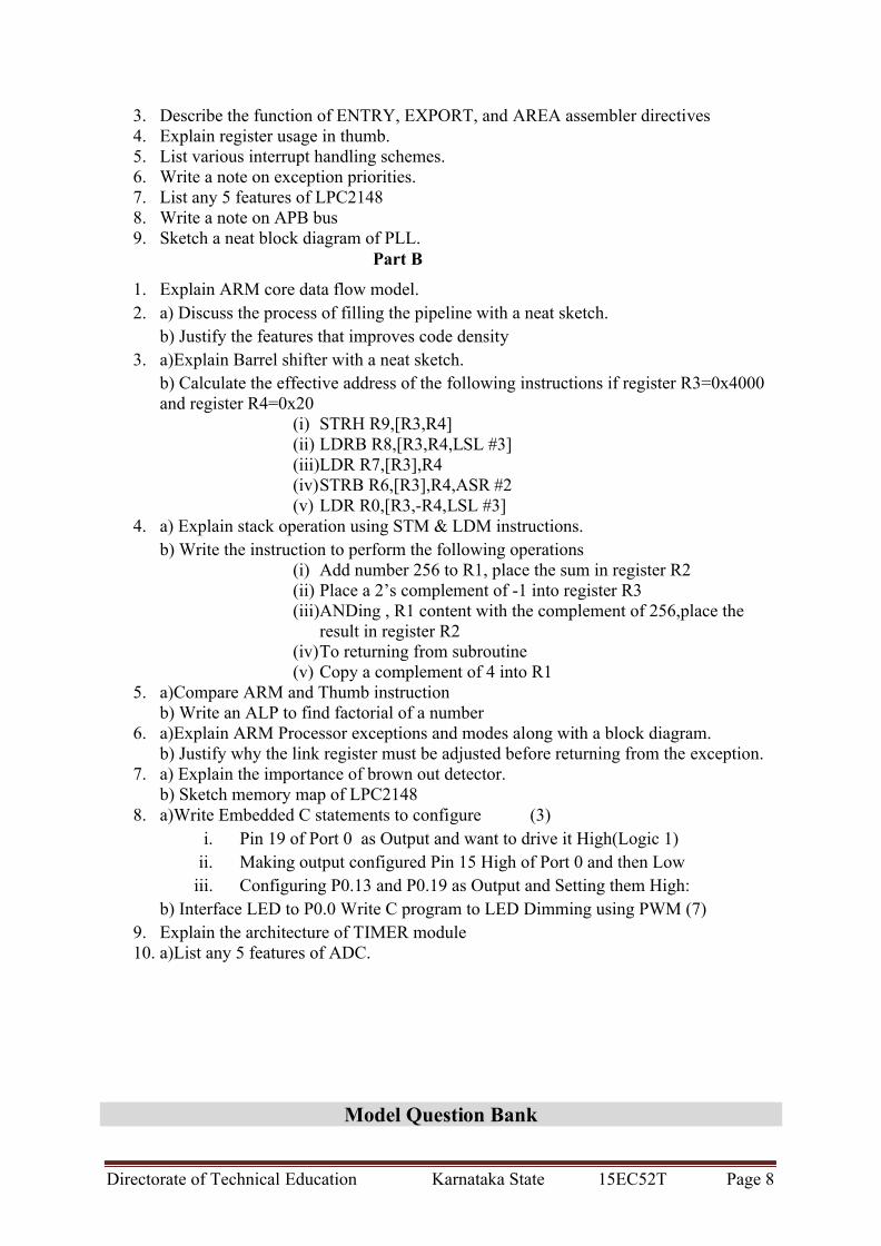
3. Describe the function of ENTRY, EXPORT, and AREA assembler directives4. Explain register usage in thumb.5. List various interrupt handling schemes.6. Write a note on exception priorities.7. List any 5 features of LPC21488. Write a note on APB bus9. Sketch a neat block diagram of PLL.
Part B
1. Explain ARM core data flow model.2. a) Discuss the process of filling the pipeline with a neat sketch.
b) Justify the features that improves code density3. a)Explain Barrel shifter with a neat sketch.
b) Calculate the effective address of the following instructions if register R3=0x4000 and register R4=0x20
(i) STRH R9,[R3,R4](ii) LDRB R8,[R3,R4,LSL #3](iii)LDR R7,[R3],R4(iv)STRB R6,[R3],R4,ASR #2(v) LDR R0,[R3,-R4,LSL #3]
4. a) Explain stack operation using STM & LDM instructions.b) Write the instruction to perform the following operations
(i) Add number 256 to R1, place the sum in register R2(ii) Place a 2’s complement of -1 into register R3(iii)ANDing , R1 content with the complement of 256,place the
result in register R2(iv)To returning from subroutine(v) Copy a complement of 4 into R1
5. a)Compare ARM and Thumb instructionb) Write an ALP to find factorial of a number
6. a)Explain ARM Processor exceptions and modes along with a block diagram.b) Justify why the link register must be adjusted before returning from the exception.
7. a) Explain the importance of brown out detector.b) Sketch memory map of LPC2148
8. a)Write Embedded C statements to configure (3)i. Pin 19 of Port 0 as Output and want to drive it High(Logic 1)
ii. Making output configured Pin 15 High of Port 0 and then Low iii. Configuring P0.13 and P0.19 as Output and Setting them High:
b) Interface LED to P0.0 Write C program to LED Dimming using PWM (7)9. Explain the architecture of TIMER module10. a)List any 5 features of ADC.
Model Question Bank
Directorate of Technical Education Karnataka State 15EC52T Page 9
Unit -1: ARM Embedded System and Arm Processor Fundamentals
5MarksRemember
1. List advantages & drawbacks of RISC2. List the features of ARM instructions suitable for embedded applications.3. List the special features of ARM processor design. 4. Define pipelining & high code density.5. Define processor modes. List all different processor modes. 6. Define banked registers. Explain 7. Describe the functions of flags of CPSR register. 8. Describe the functions of IFT bits of CPSR register.
Understand1. Explain AMBA bus protocol.2. Explain the active registers used in user mode.3. Explain 3-stage pipe line.4. Explain processor modes.
5. Explain the role of software components in an embedded systemApplication
1. List the applications of ARM processor.2. Sketch a neat ARM core data flow model.3. Write the advantages & disadvantages of pipelining.4. Discuss the process of filling the pipeline with a neat sketch.
Analyse1. justify how ARM is suited to perform DSP type function 2. justify how ARM is suitable for mobile applications3. justify the features that improves code density
10 MarksUnderstand
1. a) Explain AMBA bus protocol. ( 7 )b) Discuss mode bits of CPSR register.( 3 )
2. a) Explain the two architectural levels of Bus. ( 3 )b) Explain 3-stage pipelining of ARM-7 with example. ( 7 )
3. a) Explain register file of ARM processor with a neat sketch. ( 7 )b) Explain the function of special function registers of ARM. ( 3 )
4. a) Explain different processor modes. ( 7 )b) Explain the AMBA bus variants. ( 3 )
5. Explain banked registers with a neat diagram. 6. Explain the bit structure of CPSR. 7. Explain ARM core data flow model. 8. Explain the block diagram of ARM based embedded device.
Unit-2: ARM Instruction Set
Course Title : ARM Controller Course Code: 15EC52T
Directorate of Technical Education Karnataka State 15EC52T Page 10
5MarksUnderstanding
1. Explain conditional execution with an example. 2. Explain MAC unit with an example.3. Explain Barrel shifter with a neat sketch.4. Explain 5 different shift operations that can be used with Barrel shifter. 5. List compare instructions & Write the useful of AND, ORR, EOR instructions 6. Describe the difference between ADR & ADRL
Application1. List the data processing instructions with one example each.2. Explain stack operation using STM & LDM instructions.3. Explain SWAP & SWI instructions with example 4. Explain AND & EOR instructions with example 5. Explain TST & TEQ instructions with example 6. Write a note on software interrupt instruction.
Analyse1. Predict the operation performed by the execution of each compare instruction2. Calculate the effective address of the following instructions if register R3=0x4000
and register R4=0x20(i) STRH R9,[R3,R4](ii) LDRB R8,[R3,R4,LSL #3](iii)LDR R7,[R3],R4(iv)STRB R6,[R3],R4,ASR #2(v) LDR R0,[R3,-R4,LSL #3]
Evaluate 1. Distinguish between post & pre indexed addressing mode with an example
Create1. Test whether the following instruction are pre or post indexed addressing mode
(i) STR R6,[R4,#4](ii) LDR R3,[R12],#6(iii)LDRB R4,[R3,R2](iv)LDR R6,[R0,R1,ROR #6](v) STR R3,[R0,R5,LSL #3]
2. Write the instruction to perform the following operations(i) Add number 256 to R1, place the sum in register R2(ii) Place a 2’s complement of -1 into register R3(iii)ANDing , R1 content with the complement of 256,place the result in
register R2(iv)To returning from subroutine(v) Copy a complement of 4 into R1
Unit-3: Introduction to THUMB and ARM Programming5Marks
Remember1. Describe the function of ENTRY, EXPORT, and AREA assembler directives2. Describe the function of EQU, SPACE,ALIGN assembler directives3. Describe the function of DCD,DCB,DCW assembler directives
Understand1. Explain register usage in thumb.2. Explain ARM- THUMB networking using BLX instruction3. Explain ARM- THUMB networking using BX instruction
Directorate of Technical Education Karnataka State 15EC52T Page 11
4. Explain the structure of ARM assembly language formatApplication
1. Compare ARM & thumb instructions. 2. Write an ALP to add two 64 bit numbers.3. Write an ALP to find factorial of a number4. Write an ALP to find length of a null terminated string5. Write an ALP to multiply two 16 bit numbers6. Write an ALP to find smallest number in an array7. Write an ALP to find largest number in an array
Evaluate1. Justify how code density will be improved using Thumb 2. Justify why interrupt stack at the top of user stack memory
Unit-4:Exception and Interrupt handling schemes5 Marks
Remember1. Define exception, interrupt, interrupt vector table2. Define the terms interrupt latency& list the methods to minimize latency3. List function of the instructions used in the vector table.4. List various interrupt handling schemes.
Understand1. Explain vector table2. Discus link register offsets3. Explain exception handling4. Explain interrupt latency with diagram.5. Explain interrupt stack design with a neat sketch6. Explain the action on entering exception7. Explain the action on leaving the exception
Application1. Write a note on exception priorities.2. Write a note on interrupts 3. Write code for enabling IRQ& FIQ interrupts.4. Write code for disabling IRQ& FIQ interrupts.5. Distinguish between nested & non-nested interrupt handler.
Analyse1. Justify why the link register must be adjusted before returning from the exception.
2. Differentiate between interrupts and exceptions10 Marks
Understand1. Explain ARM Processor exceptions and modes along with a block diagram.2. Explain IRQ & FIQ exceptions with example.3. Explain non-nested interrupt handler with a neat sketch.4. Explain nested interrupt handler with a neat sketch.
Unit-5: LPC2148 ARM CPU5 Marks
Remember 1. List any 5 features of LPC21482. List any 5 applications LPC21483. List any 5 features of SPI4. List any 5 features of RTC
Directorate of Technical Education Karnataka State 15EC52T Page 12
5. Name any 5 features of UART6. Name any 5 features of I2C7. Name any 5 features of SSP8. Name any 5 system control units of LPC2148
Understand1. Explain the importance of brown out detector.2. Discus reset & wakeup timer3. Explain power modes
Application1. Sketch the diagram of LPC21482. Sketch memory map of LPC21483. Write a note on APB bus
Unit-6: LPC 2148 – Peripherals5 Marks
Remember1. List any 5 features of GPIO2. List the applications of GPIO3. List any 5 features of Timer in LPC21484. List any 5 features of PWM5. List any 5 features of ADC6. List the functional features of DAC7. List the different PLL registers & explain each bit function of PLLCON register8. Define timer, PLL, PWM, SPI, RTC9. List Rules for single &double edge controlled PWM outputs10. Name the applications of timer
. Understand1. Explain pin connect block of LPC21482. Explain legacy GPIO registers3. Explain enhanced featured GPIO registers4. Explain the operation of PLL in LPC21485. Explain the bit structure of PLLCFG register6. Explain the bit structure of PLLSTAT register7. Describe bit structure of DACR register
Application 11. Sketch a neat block diagram of PLL.12. Write the procedure for PLL frequency calculation13. Sketch a neat block diagram of TIMER14. Write Embedded C statements to configure
iv. Pin 19 of Port 0 as Output and want to drive it High(Logic 1)v. Making output configured Pin 15 High of Port 0 and then Low
vi. Configuring P0.13 and P0.19 as Output and Setting them High:vii. Configuring 1st 16 Pins of Port 0 (P0.0 to P0.15) as Output and Setting
them High15. Write C program to interface LEDs to all pins in port 0 (P0.0 to P0.15) make
repeatedly blink all LEDs High then Low then High and so on (introduce some delay).
16. Interface switch to P0.7 pin and LED to P0.30 write C program to GLOW LED when switch is Pressed
Directorate of Technical Education Karnataka State 15EC52T Page 13
Evaluate 1. Choosing, FOSC = 10MHz and CCLK = 60MHz configure PLL02. Choosing, FOSC = 12MHz and requires the USB clock of 48MHz configure PLL1 3. Calculate values of PLL Configuration Register (PLLCFG) for the following
frequency specifications cclk =60MHz, pclk=15MHz. Fcco is 156 MHz to 320 MHz.10 Marks
Understand17. Explain registers used in pin connect block of LPC214818. Explain the operation of PLL in LPC2148 with a neat diagram19. Explain the architecture of TIMER module20. a) Describe bit structure of DACR register ( 5)
b) Explain each bit function of PLLCON register ( 5 )Application
1. a)Sketch a neat block diagram of PLL.(5)b) Write the procedure for PLL frequency calculation (5)
2. Write C code to set up, initialize and connect PLL0 to get CCLK & PCLK @ 60Mhz when input clock from Crystal is 12Mhz
3. Write c program to interface LEDs to Port0, which flashes a LED every half second using timer.
4. Write C program to generate sine wave using PWM5. Interface LED to P0.0 Write C program to LED Dimming using PWM 6. Write C program to Interfacing temperature sensor with LPC2148, read temperature
from temperature sensor and it display into PC through serial port.7. Generate ramp waveform from LPC2148 microcontroller using DAC.
End


