Embed Size (px)
Citation preview

Università di Pisa
!"#$%&'(($)* +",-..-%%/.')* !"#$%&'(#$) *+,-$) +.) /"-01'2-"3'+"#$) 4#56+"07#3-,) 8(9+&&:%07#55'-5);5#"3'3&+53)*,000*12-.3-%($/.3*/.*04'%(2/.*5'6$%'3)*!")*7)*88"*9:9:*;*9:<=)*><?9?@**
Analytical Model of One-Dimensional Carbon-Based Schottky-Barrier Transistors
#$%&%'()*+,--)'5$8-2($A'.(/*B$*,.C'C.'2$-*B'44D,.E/2A-F$/.'G*04'((2/.$%-)*,.E/2A-($%-)*1'4'%/AH.$%-F$/.$)*
I.$6'23$(J*B$*!$3-*
.)/0,11,'2$33$**%3,'5$8-2($A'.(/*B$*,.C'C.'2$-*B'44D,.E/2A-F$/.'G*04'((2/.$%-)*,.E/2A-($%-)*1'4'%/AH.$%-F$/.$)*
I.$6'23$(J*B$*!$3-*
1616 IEEE TRANSACTIONS ON ELECTRON DEVICES, VOL. 57, NO. 7, JULY 2010
Analytical Model of One-Dimensional Carbon-BasedSchottky-Barrier Transistors
Paolo Michetti and Giuseppe Iannaccone, Senior Member, IEEE
Abstract—Nanotransistors typically operate in far-from-equilibrium (FFE) conditions, which cannot be described neitherby drift diffusion nor by purely ballistic models. In carbon-basednanotransistors, source and drain contacts are often characterizedby the formation of Schottky barriers (SBs), with strong influenceon transport. In this paper, we present a model for 1-D field-effecttransistors, taking into account on equal footing both SB contactsand FFE transport regime. Intermediate transport is introducedwithin the Büttiker’s probe approach to dissipative transport,in which a nonballistic transistor is seen as a suitable series ofindividually ballistic channels. Our model permits the study of theinterplay of SBs and ambipolar FFE transport and, in particular,of the transition between SB- and dissipation-limited transports.
Index Terms—Ballistic transport, Büttiker probes, carbonnanotubes (CNTs), carbon transistors, compact model, far-from-equilibrium (FFE) transport, graphene, Schottky barrier (SB).
I. INTRODUCTION
S INCE THE isolation of graphene in sheets [1], [2], withtheir exceptionally promising high mobility [3], graphene-
related materials have attracted much interest for their possibleapplication in nanoelectronic devices. In particular, semicon-ducting carbon nanotubes (CNTs) [4] and single-layer or bi-layer graphene nanoribbons (GNRs) [5] have been successfullyemployed in quasi-1-D nanotransistors.
An important issue related to carbon-based channels is thenature of metallic contact at the source and drain, which canlead to different pinnings of the Fermi level and, consequently,to the formation of ohmic or Schottky contacts [6], [7]. Thepresence of Schottky-barrier (SB) contacts can have dramaticeffects on device performance, because charge injection issubordinated to a tunneling process. However, in nanodeviceswith reduced oxide thickness, tunneling phenomena at thesource and drain are favored, and while they often limit per-formance in conventional transistors, their exploitation is at the
Manuscript received August 24, 2009; revised March 18, 2010; acceptedMarch 22, 2010. Date of publication May 24, 2010; date of current versionJune 23, 2010. This work was supported in part by the EC Seventh FrameworkProgram through Project GRAND under Contract 215752, by the Network ofExcellence Nanosil under Contract 216171, and by the European Science Foun-dation EUROCORES Program “Fundamentals of Nanoelectronics,” funded byCNR and the EC Sixth Framework Program through Project Dewint underContract ERAS-CT-2003-980409. The review of this paper was arranged byEditor M. J. Deen.
P. Michetti is with the Dipartimento di Ingegneria dell’Informazione, Univer-sitá di Pisa, 56122 Pisa, Italy, and also with the Institute for Theoretical Physicsand Astrophysics, University of Würzburg, 97070 Würzburg, Germany (e-mail:[email protected]).
G. Iannaccone is with the Dipartimento di Ingegneria dell’Informazione,Universitá di Pisa, 56122 Pisa, Italy (e-mail: [email protected]).
Color versions of one or more of the figures in this paper are available onlineat http://ieeexplore.ieee.org.
Digital Object Identifier 10.1109/TED.2010.2049219
core of the concept of tunneling field-effect transistors (FETs)[8]. Indeed, theoretical investigations show that carbon-basedtunneling FETs, such as the ones based on bilayer graphene[9] or epitaxial graphene on SiC substrates [10], can offer apotential route for low-power electronics beyond CMOS.
Transport in nanotransistors is certainly far from equilibriumbut is still not fully ballistic, and currents are much lower thanthose predicted by ballistic models [11]. While it is perfectlyclear that inelastic scattering may arise from the interactionof carriers with phonons and impurities, it is rather complexto take into account microscopically its effect on transport. Apowerful phenomenological attempt to deal with carrier relax-ation and decoherence was based on the Büttiker virtual probeapproach [12], [13], in which inelastic scattering is thoughtas localized in special points, spaced by a length defined as“mean free path.” The Büttiker approach was also introducedin microscopical models based on tight-binding Hamiltonians[14], and recently extended to deal, via a quantum Langevinapproach, with 1-D conductors [15]. In [16], the Büttiker probeapproach to inelastic scattering was employed in a simulation,based on the nonequilibrium Green’s function formalism, of anonballistic silicon nanowire transistor.
A fully microscopical analysis of inelastic scattering dueto specific mechanisms such as phonon scattering, with thenonequilibrium Green’s functions approach, has also been ad-dressed by adding a proper self energy correction on a site-representation propagating Hamiltonian by Jin et al. [17] andGilbert et al. [18], [19].
As far as analytical models are concerned, transport in quasi-1-D FETs is generally treated as purely ballistic or with adrift-diffusion assumption as in [20]–[22]. A largely invokedapproach to treat partially ballistic transport, including theeffects of backscattering, was proposed by Lundstrom [23].This approach, which is easily included as a correction toballistic models, has the merit of offering a very simple andsynthetic picture but does not allow a full description of theseamless transition from ballistic to quasi-equilibrium drift-diffusion transport. Recently, a rigorous semianalytical modelbased on the Büttiker virtual probe approach [12], [13] hasbeen conceived, in which a nonballistic transistor is seen as asuitable chain of N ballistic channels, where N is the ratio ofthe channel length to the mean free path, or, equivalently, as aseries of a drift-diffusion FET and a ballistic FET [24]–[26].
In this paper, we propose a semianalytical model based onthe virtual probe approach, which describes 1-D FETs, treatingon equal footing SB contacts and far-from-equilibrium (FFE)transport conditions. In Section II, we summarize the generalanalytical description of GNR subbands, density of states,
0018-9383/$26.00 © 2010 IEEE
Authorized licensed use limited to: UNIVERSITA PISA S ANNA. Downloaded on July 26,2010 at 07:52:31 UTC from IEEE Xplore. Restrictions apply.
MICHETTI AND IANNACCONE: ANALYTICAL MODEL OF CARBON-BASED SB TRANSISTORS 1617
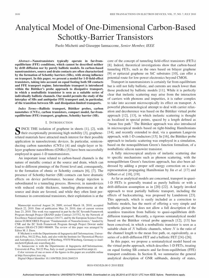
Fig. 1. Sketch of a DG-GNR FET, considered as an example for the applica-tion of our model.
and equilibrium charge density, extensible also to the CNTcase. In Section III, we present a WKB approximation of thetunneling probability through SB contacts, yielding analyticalexpressions for the transmission based on two different levelsof approximation for the energy dispersion curves of GNRs (orCNTs). In Section IV, a model for a single ballistic transistorwith SB contacts is presented, compared with the data fromnumerical simulations. In Section V, we propose a compactmodel, based on the Büttiker virtual probe approach that is ableto deal with both intermediate (I) transport and SB contacts, anduse it to study the interplay of SB and dissipative transport.
II. DISPERSION RELATION AND DENSITY OF STATES
The dispersion curve of an armchair GNR (A-GNR) with Ndimer lines can be obtained analytically by cutting techniques,analogous to that used for CNTs in [27], from the 2-D graphenetight-binding dispersion. The subband dispersion curves corre-spond to 1-D segments of the graphene Brillouin zone with theconfined wavevector quantized as k! = !"/(N + 1), with " =1, 2, . . . , N . The dispersion curve of the subband ", referred toas midgap, is
E!(k) = ±V
!1 + 4 cos
!3ak
2A! + 4A2
!
"1/2
(1)
with A! = cos(!"/(N + 1)), and V = 2.7 eV is the tight-binding hopping parameter. We note here that a dispersionrelation that is totally analogous to (1) applies to zigzag (N, 0)CNT, with the only difference that, in the place of A!, we haveto use ACNT
! = cos(!"/N), where " is the subband index ofCNTs [28]. Therefore, much of the results for GNRs obtainedhere and in the succeeding sections of this paper, with theexclusion of the edge corrections, can be directly generalizedto the zigzag CNT case by properly modifying the valuesof parameters accounting for the screening and geometricalproperties (Fig. 1).
The edge of the "th subband E!(0) is expressed as
E!(0) = ±V (1 + 2A!). (2)
Let us note that the lowest lying subband is given by the valueof " for which A! + (1/2) is minimum. The edges of the
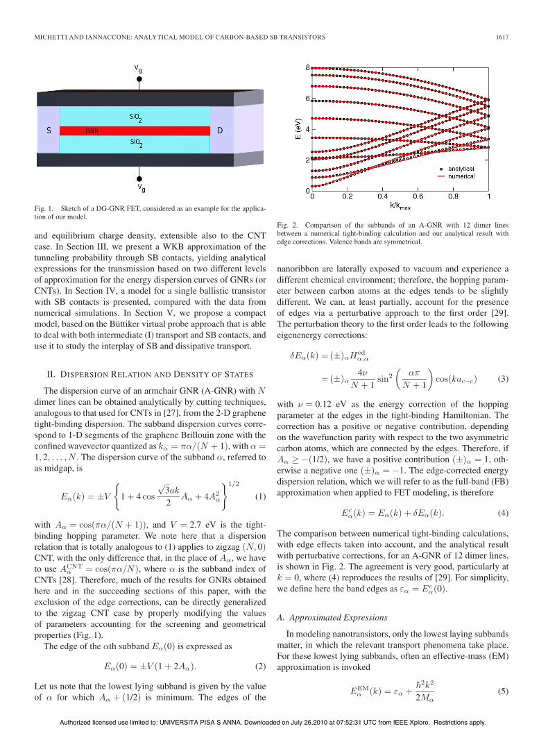
Fig. 2. Comparison of the subbands of an A-GNR with 12 dimer linesbetween a numerical tight-binding calculation and our analytical result withedge corrections. Valence bands are symmetrical.
nanoribbon are laterally exposed to vacuum and experience adifferent chemical environment; therefore, the hopping param-eter between carbon atoms at the edges tends to be slightlydifferent. We can, at least partially, account for the presenceof edges via a perturbative approach to the first order [29].The perturbation theory to the first order leads to the followingeigenenergy corrections:
#E!(k) = (±)!Hed!,!
=(±)!4$
N + 1sin2
#"!
N + 1
$cos(kac"c) (3)
with $ = 0.12 eV as the energy correction of the hoppingparameter at the edges in the tight-binding Hamiltonian. Thecorrection has a positive or negative contribution, dependingon the wavefunction parity with respect to the two asymmetriccarbon atoms, which are connected by the edges. Therefore, ifA! # "(1/2), we have a positive contribution (±)! = 1, oth-erwise a negative one (±)! = "1. The edge-corrected energydispersion relation, which we will refer to as the full-band (FB)approximation when applied to FET modeling, is therefore
Ec!(k) = E!(k) + #E!(k). (4)
The comparison between numerical tight-binding calculations,with edge effects taken into account, and the analytical resultwith perturbative corrections, for an A-GNR of 12 dimer lines,is shown in Fig. 2. The agreement is very good, particularly atk = 0, where (4) reproduces the results of [29]. For simplicity,we define here the band edges as %! = Ec
!(0).
A. Approximated Expressions
In modeling nanotransistors, only the lowest laying subbandsmatter, in which the relevant transport phenomena take place.For these lowest lying subbands, often an effective-mass (EM)approximation is invoked
EEM! (k) = %! +
!2k2
2M!(5)
Authorized licensed use limited to: UNIVERSITA PISA S ANNA. Downloaded on July 26,2010 at 07:52:31 UTC from IEEE Xplore. Restrictions apply.
1618 IEEE TRANSACTIONS ON ELECTRON DEVICES, VOL. 57, NO. 7, JULY 2010
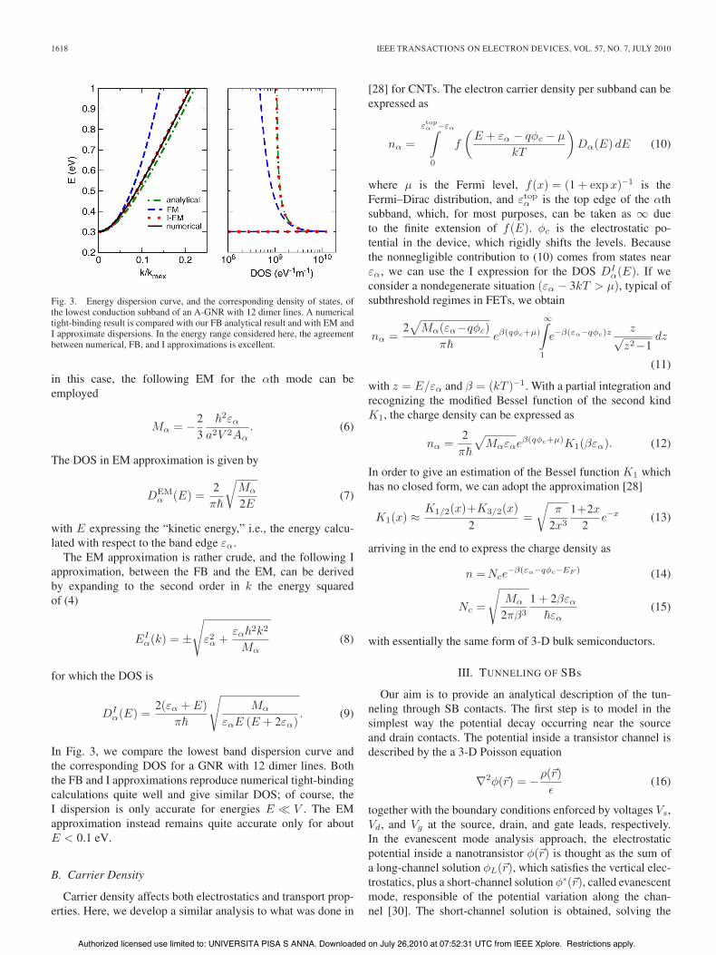
Fig. 3. Energy dispersion curve, and the corresponding density of states, ofthe lowest conduction subband of an A-GNR with 12 dimer lines. A numericaltight-binding result is compared with our FB analytical result and with EM andI approximate dispersions. In the energy range considered here, the agreementbetween numerical, FB, and I approximations is excellent.
in this case, the following EM for the "th mode can beemployed
M! = "23
!2%!
a2V 2A!. (6)
The DOS in EM approximation is given by
DEM! (E) =
2!!
%M!
2E(7)
with E expressing the “kinetic energy,” i.e., the energy calcu-lated with respect to the band edge %!.
The EM approximation is rather crude, and the following Iapproximation, between the FB and the EM, can be derivedby expanding to the second order in k the energy squaredof (4)
EI!(k) = ±
&
%2! +
%!!2k2
M!(8)
for which the DOS is
DI!(E) =
2(%! + E)!!
&M!
%!E (E + 2%!). (9)
In Fig. 3, we compare the lowest band dispersion curve andthe corresponding DOS for a GNR with 12 dimer lines. Boththe FB and I approximations reproduce numerical tight-bindingcalculations quite well and give similar DOS; of course, theI dispersion is only accurate for energies E $ V . The EMapproximation instead remains quite accurate only for aboutE < 0.1 eV.
B. Carrier Density
Carrier density affects both electrostatics and transport prop-erties. Here, we develop a similar analysis to what was done in
[28] for CNTs. The electron carrier density per subband can beexpressed as
n! =
"top! ""!'
0
f
#E + %! " q&c " µ
kT
$D!(E) dE (10)
where µ is the Fermi level, f(x) = (1 + expx)"1 is theFermi–Dirac distribution, and %top
! is the top edge of the "thsubband, which, for most purposes, can be taken as % dueto the finite extension of f(E). &c is the electrostatic po-tential in the device, which rigidly shifts the levels. Becausethe nonnegligible contribution to (10) comes from states near%!, we can use the I expression for the DOS DI
!(E). If weconsider a nondegenerate situation (%! " 3kT > µ), typical ofsubthreshold regimes in FETs, we obtain
n! =2(
M!(%!"q&c)!! e#(q$c+µ)
%'
1
e"#("!"q$c)z z!z2"1
dz
(11)
with z = E/%! and ' = (kT )"1. With a partial integration andrecognizing the modified Bessel function of the second kindK1, the charge density can be expressed as
n! =2!!
(M!%!e#(q$c+µ)K1('%!). (12)
In order to give an estimation of the Bessel function K1 whichhas no closed form, we can adopt the approximation [28]
K1(x) &K1/2(x)+K3/2(x)
2=
%!
2x3
1+2x
2e"x (13)
arriving in the end to express the charge density as
n = Nce"#("!"q$c"EF ) (14)
Nc =
&M!
2!'3
1 + 2'%!
!%!(15)
with essentially the same form of 3-D bulk semiconductors.
III. TUNNELING OF SBs
Our aim is to provide an analytical description of the tun-neling through SB contacts. The first step is to model in thesimplest way the potential decay occurring near the sourceand drain contacts. The potential inside a transistor channel isdescribed by the a 3-D Poisson equation
'2&((r) = ")((r)*
(16)
together with the boundary conditions enforced by voltages Vs,Vd, and Vg at the source, drain, and gate leads, respectively.In the evanescent mode analysis approach, the electrostaticpotential inside a nanotransistor &((r) is thought as the sum ofa long-channel solution &L((r), which satisfies the vertical elec-trostatics, plus a short-channel solution &(((r), called evanescentmode, responsible of the potential variation along the chan-nel [30]. The short-channel solution is obtained, solving the
Authorized licensed use limited to: UNIVERSITA PISA S ANNA. Downloaded on July 26,2010 at 07:52:31 UTC from IEEE Xplore. Restrictions apply.
MICHETTI AND IANNACCONE: ANALYTICAL MODEL OF CARBON-BASED SB TRANSISTORS 1619
Laplace equation for the device with an adequate expansionin harmonic functions. As a matter of fact, the short-channelsolution near the source contact results in an exponential profile
&(((r) ) R((r*)e"z/% (17)
where R((r*) describes the solution in the channel cross sectionand + comes to be a natural scale length for the potentialvariation in the device. The actual value of + depends onthe details of the device geometry; however, in a double-gate(DG) configuration, and considering that, in general, in carbon-based FET, the oxide thickness is significantly larger than thechannel thickness, the asymptotic value + = (2tox + tch)/!can be assumed. In the case of a cylindrical GAA-CNT FET,an explicit calculation of + via evanescent mode analysis hasbeen performed in [31].
We follow this line and assume that the channel potentialrigidly shifts the confinement eigenvalues %!, where " runson the different subbands. Now, we are interested only in thepotential inside the restricted zone of the graphene channel&c(z), in which it can be assumed as a constant (which isstrictly true in subthreshold regimes), and we consider itsvariation only along the channel direction. The long-channelsolution inside the channel is reduced to &L((r) & &c, where &c
is solely imposed by the vertical electrostatics, while the short-channel solution has the form (17). Therefore, the potential inthe channel &c(z) can be expressed as
&c(z) = &c +As
qe"z/% (18)
with &c = &(%) fixed by the vertical electrostatics and As
imposed by the boundary condition at the SB contact As =E(s)
SB " %L + q&c, where L refers to the lowest lying subband,due to the Fermi level pinning at the metal/semiconductorinterface. E(s)
SB is the SB height on the first conduction subbandwith respect to the source Fermi level. The charge injectedfrom the source with energy lower than the barrier has totunnel in order to reach the channel. We need to calculatethe transmission through an exponential decaying barrier ofthe kind
ESB(z) = As e"z/% (19)
with the height As dependent on the electrostatic potential&c. We note however that if the band bending exceeds theenergy gap 2%!, a carrier with energy 0 < E < As " 2%! willexperience an SB of a height As = E + 2%!.
In order to estimate the behavior of a nanotransistor, it isessential to accurately describe the tunneling phenomena, bothin traditional FETs and in TFETs. In this section, we comparethe tunneling calculated with WKB approximation in an FBapproach (FB-WKB), within the EM approach (EM-WKB),and I approximation (I-WKB). FB-WKB is more complex toimplement and requires a numerical solution of the integral
ln (T (E)) = "2
z2'
z1
I [kz(zE)] dz. (20)
While for the other two, an analytical expression for the tunnel-ing T (E) can be obtained.
A. EM-WKB Approximation
The transmission coefficient obtained via the WKB approxi-mation is given as
T (E)=e"2
) z2z1
!2m!/!2(ESB(z)"E)dz
, E < As
1, E # As(21)
where z1 and z2 are the classical turning points
z1 = 0 z2 = "+ ln*
E
As
+. (22)
The transmission coefficient can be analytically calculated in
lnT (E) = "4+
%m!(As " E)
!2
+,1"
%E
As"Etan"1
-%As " E
E
./. (23)
B. I-WKB Approximation
Let us consider a dispersion curve of the kind (8). The turningpoints with a barrier like (19) are the same as (22), but now,under the barrier, the imaginary part of the wave vector as afunction of energy is given by
I[kz, E] =%
M!
!2%!
0a2 "
1b " e"
z"
22 (24)
with
a =%!
Asb = a +
E
As.
The integration (20), for E < As, leads to the WKB tunnelingprobability
lnT (E) =2As+
!M!!
!2%!
*"b
#!
2" arctan
b " 1R1
$" R1
+ R2
#! " arctan
R1R2
a2 " b2 + b
$+
(25)
where we introduced the abbreviations
R1 =(
a2 " (b " 1)2 R2 =(
b2 " a2.
C. FB-WKB Approximation
For an A-GNR, subband dispersion curves are in the form(1), from which we can express the wave vector as a functionof energy as
k =2
a!
3arccos x (26)
Authorized licensed use limited to: UNIVERSITA PISA S ANNA. Downloaded on July 26,2010 at 07:52:31 UTC from IEEE Xplore. Restrictions apply.
1620 IEEE TRANSACTIONS ON ELECTRON DEVICES, VOL. 57, NO. 7, JULY 2010
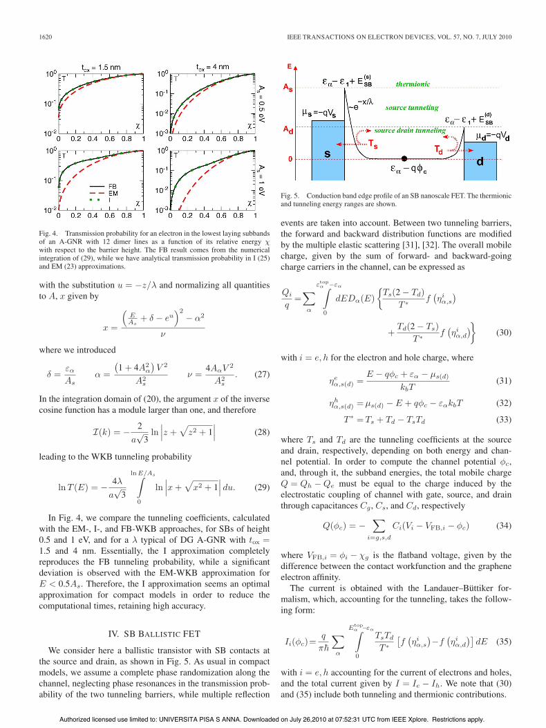
Fig. 4. Transmission probability for an electron in the lowest laying subbandsof an A-GNR with 12 dimer lines as a function of its relative energy !with respect to the barrier height. The FB result comes from the numericalintegration of (29), while we have analytical transmission probability in I (25)and EM (23) approximations.
with the substitution u = "z/+ and normalizing all quantitiesto A, x given by
x =
3EAs
+ # " eu42
" "2
$
where we introduced
# =%!
As" =
11 + 4A2
!
2V 2
A2s
$ =4A!V 2
A2s
. (27)
In the integration domain of (20), the argument x of the inversecosine function has a module larger than one, and therefore
I(k) = " 2
a!
3ln
555z +(
z2 + 1555 (28)
leading to the WKB tunneling probability
lnT (E) = " 4+
a!
3
lnE/As'
0
ln555x +
(x2 + 1
555 du. (29)
In Fig. 4, we compare the tunneling coefficients, calculatedwith the EM-, I-, and FB-WKB approaches, for SBs of height0.5 and 1 eV, and for a + typical of DG A-GNR with tox =1.5 and 4 nm. Essentially, the I approximation completelyreproduces the FB tunneling probability, while a significantdeviation is observed with the EM-WKB approximation forE < 0.5As. Therefore, the I approximation seems an optimalapproximation for compact models in order to reduce thecomputational times, retaining high accuracy.
IV. SB BALLISTIC FET
We consider here a ballistic transistor with SB contacts atthe source and drain, as shown in Fig. 5. As usual in compactmodels, we assume a complete phase randomization along thechannel, neglecting phase resonances in the transmission prob-ability of the two tunneling barriers, while multiple reflection
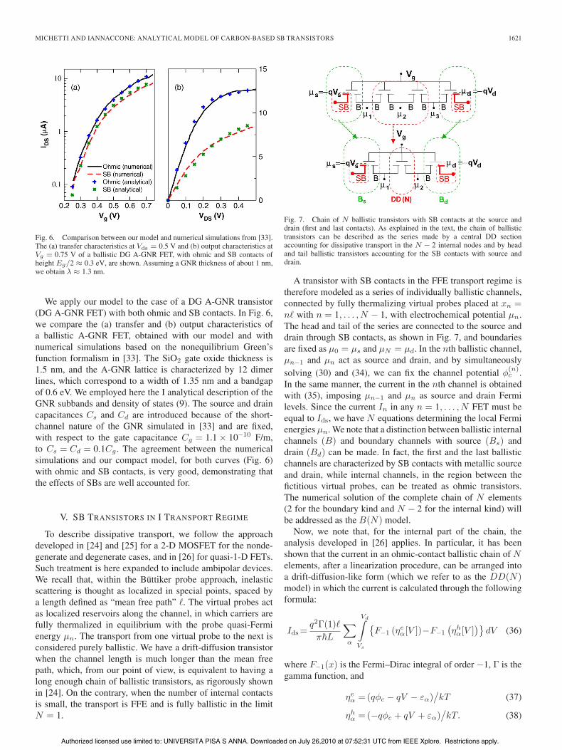
Fig. 5. Conduction band edge profile of an SB nanoscale FET. The thermionicand tunneling energy ranges are shown.
events are taken into account. Between two tunneling barriers,the forward and backward distribution functions are modifiedby the multiple elastic scattering [31], [32]. The overall mobilecharge, given by the sum of forward- and backward-goingcharge carriers in the channel, can be expressed as
Qi
q=
6
!
"top! ""!'
0
dED!(E)7
Ts(2 " Td)T ( f
1,i
!,s
2
+Td(2 " Ts)
T ( f1,i
!,d
28(30)
with i = e, h for the electron and hole charge, where
,e!,s(d) =
E " q&c + %! " µs(d)
kbT(31)
,h!,s(d) = µs(d) " E + q&c " %!kbT (32)
T ( = Ts + Td " TsTd (33)
where Ts and Td are the tunneling coefficients at the sourceand drain, respectively, depending on both energy and chan-nel potential. In order to compute the channel potential &c,and, through it, the subband energies, the total mobile chargeQ = Qh " Qe must be equal to the charge induced by theelectrostatic coupling of channel with gate, source, and drainthrough capacitances Cg , Cs, and Cd, respectively
Q(&c) = "6
i=g,s,d
Ci(Vi " VFB,i " &c) (34)
where VFB,i = &i " -g is the flatband voltage, given by thedifference between the contact workfunction and the grapheneelectron affinity.
The current is obtained with the Landauer–Büttiker for-malism, which, accounting for the tunneling, takes the follow-ing form:
Ii(&c)=q
!!6
!
Etop! ""!'
0
TsTd
T (
9f
1,i
!,s
2"f
1,i
!,d
2:dE (35)
with i = e, h accounting for the current of electrons and holes,and the total current given by I = Ie " Ih. We note that (30)and (35) include both tunneling and thermionic contributions.
Authorized licensed use limited to: UNIVERSITA PISA S ANNA. Downloaded on July 26,2010 at 07:52:31 UTC from IEEE Xplore. Restrictions apply.
MICHETTI AND IANNACCONE: ANALYTICAL MODEL OF CARBON-BASED SB TRANSISTORS 1621
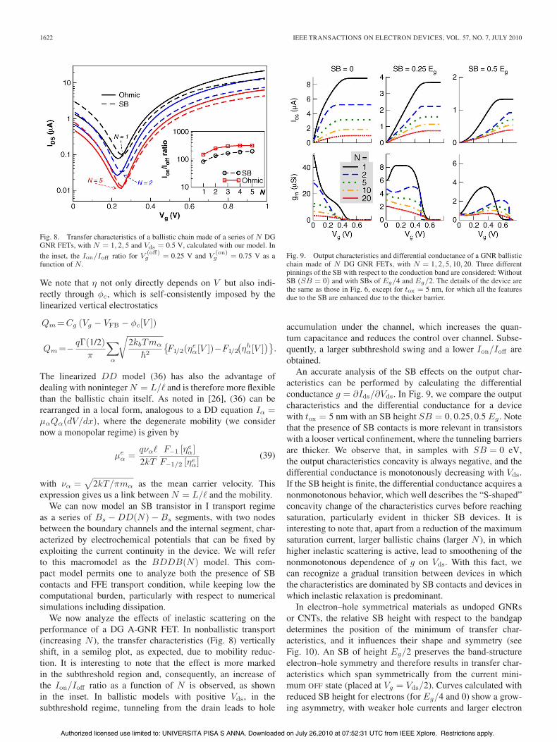
Fig. 6. Comparison between our model and numerical simulations from [33].The (a) transfer characteristics at Vds = 0.5 V and (b) output characteristics atVg = 0.75 V of a ballistic DG A-GNR FET, with ohmic and SB contacts ofheight Eg/2 ! 0.3 eV, are shown. Assuming a GNR thickness of about 1 nm,we obtain " ! 1.3 nm.
We apply our model to the case of a DG A-GNR transistor(DG A-GNR FET) with both ohmic and SB contacts. In Fig. 6,we compare the (a) transfer and (b) output characteristics ofa ballistic A-GNR FET, obtained with our model and withnumerical simulations based on the nonequilibrium Green’sfunction formalism in [33]. The SiO2 gate oxide thickness is1.5 nm, and the A-GNR lattice is characterized by 12 dimerlines, which correspond to a width of 1.35 nm and a bandgapof 0.6 eV. We employed here the I analytical description of theGNR subbands and density of states (9). The source and draincapacitances Cs and Cd are introduced because of the short-channel nature of the GNR simulated in [33] and are fixed,with respect to the gate capacitance Cg = 1.1 + 10"10 F/m,to Cs = Cd = 0.1Cg . The agreement between the numericalsimulations and our compact model, for both curves (Fig. 6)with ohmic and SB contacts, is very good, demonstrating thatthe effects of SBs are well accounted for.
V. SB TRANSISTORS IN I TRANSPORT REGIME
To describe dissipative transport, we follow the approachdeveloped in [24] and [25] for a 2-D MOSFET for the nonde-generate and degenerate cases, and in [26] for quasi-1-D FETs.Such treatment is here expanded to include ambipolar devices.We recall that, within the Büttiker probe approach, inelasticscattering is thought as localized in special points, spaced bya length defined as “mean free path” .. The virtual probes actas localized reservoirs along the channel, in which carriers arefully thermalized in equilibrium with the probe quasi-Fermienergy µn. The transport from one virtual probe to the next isconsidered purely ballistic. We have a drift-diffusion transistorwhen the channel length is much longer than the mean freepath, which, from our point of view, is equivalent to having along enough chain of ballistic transistors, as rigorously shownin [24]. On the contrary, when the number of internal contactsis small, the transport is FFE and is fully ballistic in the limitN = 1.
Fig. 7. Chain of N ballistic transistors with SB contacts at the source anddrain (first and last contacts). As explained in the text, the chain of ballistictransistors can be described as the series made by a central DD sectionaccounting for dissipative transport in the N " 2 internal nodes and by headand tail ballistic transistors accounting for the SB contacts with source anddrain.
A transistor with SB contacts in the FFE transport regime istherefore modeled as a series of individually ballistic channels,connected by fully thermalizing virtual probes placed at xn =n. with n = 1, . . . , N " 1, with electrochemical potential µn.The head and tail of the series are connected to the source anddrain through SB contacts, as shown in Fig. 7, and boundariesare fixed as µ0 = µs and µN = µd. In the nth ballistic channel,µn"1 and µn act as source and drain, and by simultaneouslysolving (30) and (34), we can fix the channel potential &(n)
c .In the same manner, the current in the nth channel is obtainedwith (35), imposing µn"1 and µn as source and drain Fermilevels. Since the current In in any n = 1, . . . , N FET must beequal to Ids, we have N equations determining the local Fermienergies µn. We note that a distinction between ballistic internalchannels (B) and boundary channels with source (Bs) anddrain (Bd) can be made. In fact, the first and the last ballisticchannels are characterized by SB contacts with metallic sourceand drain, while internal channels, in the region between thefictitious virtual probes, can be treated as ohmic transistors.The numerical solution of the complete chain of N elements(2 for the boundary kind and N " 2 for the internal kind) willbe addressed as the B(N) model.
Now, we note that, for the internal part of the chain, theanalysis developed in [26] applies. In particular, it has beenshown that the current in an ohmic-contact ballistic chain of Nelements, after a linearization procedure, can be arranged intoa drift-diffusion-like form (which we refer to as the DD(N)model) in which the current is calculated through the followingformula:
Ids =q2!(1).
!!L
6
!
Vd'
Vs
;F"1 (,e
![V ])"F"1
1,h
![V ]2<
dV (36)
where F"1(x) is the Fermi–Dirac integral of order "1, ! is thegamma function, and
,e! = (q&c " qV " %!)
=kT (37)
,h! = ("q&c + qV + %!)
=kT. (38)
Authorized licensed use limited to: UNIVERSITA PISA S ANNA. Downloaded on July 26,2010 at 07:52:31 UTC from IEEE Xplore. Restrictions apply.
1622 IEEE TRANSACTIONS ON ELECTRON DEVICES, VOL. 57, NO. 7, JULY 2010
Fig. 8. Transfer characteristics of a ballistic chain made of a series of N DGGNR FETs, with N = 1, 2, 5 and Vds = 0.5 V, calculated with our model. Inthe inset, the Ion/Io! ratio for V (o!)
g = 0.25 V and V (on)g = 0.75 V as a
function of N .
We note that , not only directly depends on V but also indi-rectly through &c, which is self-consistently imposed by thelinearized vertical electrostatics
Qm = Cg (Vg " VFB " &c[V ])
Qm =" q!(1/2)!
6
!
%2kbTm!
!2
;F1/2(,e
![V ])"F1/2
1,h
![V ]2<
.
The linearized DD model (36) has also the advantage ofdealing with noninteger N = L/. and is therefore more flexiblethan the ballistic chain itself. As noted in [26], (36) can berearranged in a local form, analogous to a DD equation I! =µ!Q!(dV/dx), where the degenerate mobility (we considernow a monopolar regime) is given by
µe! =
q$!.
2kT
F"1 [,e!]
F"1/2 [,e!]
(39)
with $! =(
2kT/!m! as the mean carrier velocity. Thisexpression gives us a link between N = L/. and the mobility.
We can now model an SB transistor in I transport regimeas a series of Bs " DD(N) " Bs segments, with two nodesbetween the boundary channels and the internal segment, char-acterized by electrochemical potentials that can be fixed byexploiting the current continuity in the device. We will referto this macromodel as the BDDB(N) model. This com-pact model permits one to analyze both the presence of SBcontacts and FFE transport condition, while keeping low thecomputational burden, particularly with respect to numericalsimulations including dissipation.
We now analyze the effects of inelastic scattering on theperformance of a DG A-GNR FET. In nonballistic transport(increasing N ), the transfer characteristics (Fig. 8) verticallyshift, in a semilog plot, as expected, due to mobility reduc-tion. It is interesting to note that the effect is more markedin the subthreshold region and, consequently, an increase ofthe Ion/Io! ratio as a function of N is observed, as shownin the inset. In ballistic models with positive Vds, in thesubthreshold regime, tunneling from the drain leads to hole
Fig. 9. Output characteristics and differential conductance of a GNR ballisticchain made of N DG GNR FETs, with N = 1, 2, 5, 10, 20. Three differentpinnings of the SB with respect to the conduction band are considered: WithoutSB (SB = 0) and with SBs of Eg/4 and Eg/2. The details of the device arethe same as those in Fig. 6, except for tox = 5 nm, for which all the featuresdue to the SB are enhanced due to the thicker barrier.
accumulation under the channel, which increases the quan-tum capacitance and reduces the control over channel. Subse-quently, a larger subthreshold swing and a lower Ion/Io! areobtained.
An accurate analysis of the SB effects on the output char-acteristics can be performed by calculating the differentialconductance g = /Ids//Vds. In Fig. 9, we compare the outputcharacteristics and the differential conductance for a devicewith tox = 5 nm with an SB height SB = 0, 0.25, 0.5 Eg . Notethat the presence of SB contacts is more relevant in transistorswith a looser vertical confinement, where the tunneling barriersare thicker. We observe that, in samples with SB = 0 eV,the output characteristics concavity is always negative, and thedifferential conductance is monotonously decreasing with Vds.If the SB height is finite, the differential conductance acquires anonmonotonous behavior, which well describes the “S-shaped”concavity change of the characteristics curves before reachingsaturation, particularly evident in thicker SB devices. It isinteresting to note that, apart from a reduction of the maximumsaturation current, larger ballistic chains (larger N ), in whichhigher inelastic scattering is active, lead to smoothening of thenonmonotonous dependence of g on Vds. With this fact, wecan recognize a gradual transition between devices in whichthe characteristics are dominated by SB contacts and devices inwhich inelastic relaxation is predominant.
In electron–hole symmetrical materials as undoped GNRsor CNTs, the relative SB height with respect to the bandgapdetermines the position of the minimum of transfer char-acteristics, and it influences their shape and symmetry (seeFig. 10). An SB of height Eg/2 preserves the band-structureelectron–hole symmetry and therefore results in transfer char-acteristics which span symmetrically from the current mini-mum OFF state (placed at Vg = Vds/2). Curves calculated withreduced SB height for electrons (for Eg/4 and 0) show a grow-ing asymmetry, with weaker hole currents and larger electron
Authorized licensed use limited to: UNIVERSITA PISA S ANNA. Downloaded on July 26,2010 at 07:52:31 UTC from IEEE Xplore. Restrictions apply.
MICHETTI AND IANNACCONE: ANALYTICAL MODEL OF CARBON-BASED SB TRANSISTORS 1623
Fig. 10. Transfer characteristics of GNR devices increasing tox = 1, 3, 5 nm,calculated for Vds = 0.5 V. Ballistic chains of N = 1, 2, 5, 20 are drawn;devices without SB (SB = 0) and with SBs of Eg/4 and Eg/2 are shown.Arrows indicating the shift of the transfer characteristics curves with N arealso added as a guide for the eyes.
currents, together with a shift of the transfer characteristicminimum to lower values of Vg . This phenomenon is prominentin thicker SB devices, such as the tox = 5 nm FET, but wellobservable also in a tox = 1 nm device. The increase of thelateral confinement leads in fact to an almost linear increase ofthe SB thickness, and therefore, all tunneling processes becomeharder. As expected, if we increase the dissipative phenomena(increasing N ), a reduction of the current is observed. Moreinterestingly, while the SB = Eg/2 curves vertically shift, aspointed out with the arrows in Fig. 10, while the shift of theother curves is diagonal; note, in fact, the horizontal shift oftheir minima with N . Moreover, by increasing N , the minimaseem to converge toward the value Vg = Vds/2, which is typicalof a symmetrical ambipolar device. This is yet another signatureof the growing importance of inelastic transport over the SBcontacts. Therefore, for sufficiently well-confined FET, we canexpect in quasi-ballistic GNT/CNT devices to clearly observean SB behavior, which becomes more and more subtle indissipative regimes. To quantify the relative importance of theSB in determining the symmetry of the transfer characteristics,we made the following physical estimation: SB = 0.5Eg cor-responds to the symmetrical case; therefore, if we impose adifferent SB, the change in the conductance will be exponentialin the SB difference #ESB as
#gSB ) exp7"2tox
!! (2m#ESB)1/2
8(40)
as can be obtained estimating the differential conductance ofa device with an SB source contact at the source Fermi level.This quantity is, in fact, dominated by the tunneling coefficient(23). This difference in the conductance is relevant as long asit is greater than the conductance due to the DD(N) chain. Weobtain
0 =#gSB
gN& N exp
7"tox ( 2
!! (2m#ESB)1/2
8. (41)
Fig. 11. Ballistic index of a ballistic chain of N elementary GNR FETs withSB is varied from 0 to Eg/2 as a function of N . The source–drain voltage isset to Vds = 0.1 and 0.5 V for Vg = 0.75 V.
Employing this formula, we can calculate the N = Ns cor-responding to 0 = 1 for different SB values and oxide thick-nesses, as shown in the following table:
Ns tox = 1 tox = 3 tox = 5 (nm)
SB = 0 4 70 103
SB = 0.25Eg 7 450 104 .
Ns gives a rough estimation to the number of nodes (i.e., L/.ratio) needed to make the transfer characteristics symmetrical,in spite of the presence of an SB. As can be observed, compar-ing these values with the behavior of the curves in Fig. 10, thetox = 1 nm curves with SB = 5 and 10, respectively, for SB =0.25Eg and 0 are quite symmetrical in accordance with Ns = 4and Ns = 7 found by our calculation. The minimum of thecurve N = 10 with SB = 0.25Eg comes near the symmetricalvalues, but still misses it, being our estimation Ns = 70. Othercurves are highly asymmetric, being N $ Ns.
A typical parameter used to characterize the transport regimein quasi-ballistic devices is the ballisticity index Bindex = I/I1,which is the ratio of the actual current to the current corre-sponding to an analogous device in a purely ballistic transportregime (N = 1). In Fig. 11, we analyze the role of the SBcontacts in determining the ballisticity index as a functionof N and, therefore, as a function of the degree of inelasticrelaxation. In general, to lower SB heights corresponds to afaster variation of Bindex with N , with a sudden drop of theballisticity as a function of the number of nodes, after whicha slower decrease is observed. SBs affect, in particular, theballisticity index calculated for lower Vds, due to the concavityof the output characteristics, while larger source–drain voltagesreduce the relative importance of SB with respect to inelasticmechanisms. Calculations with tox = 5 nm reveal the increasedimportance of SB contacts and reflect the presence of theinflection in the output characteristics, with a concavity changebefore saturation. In particular, for higher value of the SB, weobserve a slower dependence of the Bindex on N , because thecurrent is calculated in a bias point of the characteristic curveof strong “s” curvature. Physically, it means that the current
Authorized licensed use limited to: UNIVERSITA PISA S ANNA. Downloaded on July 26,2010 at 07:52:31 UTC from IEEE Xplore. Restrictions apply.
1624 IEEE TRANSACTIONS ON ELECTRON DEVICES, VOL. 57, NO. 7, JULY 2010
flowing in the device is mostly limited by the injection throughthe tunneling barriers.
VI. CONCLUSION
We have presented a semianalytical model dealing withambipolar 1-D SB transistors in I transport regimes betweenfully ballistic and quasi-equilibrium, i.e., governed by the drift-diffusion model. We have introduced simplified, but accurate,descriptions of the SB profiles and of the electrostatics, andanalytical approximations of the tunneling coefficients of theSBs. We have demonstrated that an SB transistor can be mod-eled as three transistors in series, with common gate voltage.The central one is a drift-diffusion transistor, with mobilitydependent on the degree of degeneracy of the 1-D carriergas. The other two transistors are ballistic FETs with an SBcontact corresponding to the external actual contacts (source ordrain). In the case of ballistic transport, our model allows us toreproduce the results of a 3-D numerical Poisson–Schroedingersimulator. In the case of very long channel, with respect to themean free path, current is limited by the central drift-diffusiontransistor. The model allows one very directly to investigatethe transition from barrier- to channel-limited transport. Oursemianalytical model represents an accurate and simple way togain physical insights into the behavior of nanoscale transistorswith SB contacts, including most the relevant physics at a verylow computational cost. We also developed an open-versiontool, which is available on the Nanohub site under the nameFFETtool [34], solving the model discussed in this paper,restricted to the EM approximation.
REFERENCES
[1] K. S. Novoselov, A. K. Geim, S. V. Morozov, D. Jiang, Y. Zhang,S. V. Dubonos, I. V. Grigorieva, and A. A. Firsov, “Electric field effect inatomically thin carbon films,” Science, vol. 306, no. 5696, pp. 666–669,Oct. 2004.
[2] K. S. Novoselov, A. K. Geim, S. V. Morozov, D. Jiang, M. I. Katsnelson,I. V. Grigorieva, S. V. Dubonos, and A. A. Firsov, “Two-dimensionalgas of massless Dirac fermions in graphene,” Nature, vol. 438, no. 7065,pp. 197–200, Nov. 2005.
[3] A. K. Geim and K. S. Novoselov, “The rise of graphene,” Nature Mater.,vol. 6, no. 3, pp. 183–191, Mar. 2007.
[4] A. Bachtold, P. Hadley, T. Nakanishi, and C. Dekker, “Logic circuits withcarbon nanotube transistors,” Science, vol. 294, no. 5545, pp. 1317–1320,Nov. 2001.
[5] X. Li, X. Wang, L. Zhang, S. Lee, and H. Dai, “Chemically derived,ultrasmooth graphene nanoribbon semiconductors,” Science, vol. 319,no. 5867, pp. 1229–1232, Feb. 2008. 1150878.
[6] A. Javey, J. Guo, Q. Wang, M. Lundstrom, and H. Dai, “Ballistic carbonnanotube field-effect transistors,” Nature, vol. 424, no. 6949, pp. 654–657,Aug. 2003.
[7] Z. Zhou, G. Eres, R. Jin, A. Subedi, D. Mandrus, and E. Kim, “Theperformance of in situ grown Schottky-barrier single wall carbon nan-otube field-effect transistors,” Nanotechnology, vol. 20, no. 8, p. 085709,Feb. 2009.
[8] J. Knoch and J. Appenzeller, “Tunneling phenomena in carbon nanotubesfield-effect transistors,” Phys. Stat. Sol. (A), vol. 205, no. 4, pp. 679–694,Apr. 2008.
[9] G. Fiori and G. Iannaccone, “Ultralow-voltage bilayer graphene tun-nel FET,” IEEE Electron Device Lett., vol. 30, no. 10, pp. 1096–1098,Oct. 2009.
[10] P. Michetti and G. Iannaccone, “Model of tunneling transistors basedon graphene on SiC,” Appl. Phys. Lett., vol. 96, no. 13, p. 133 508,Mar. 2010.
[11] N. Singh, A. Agarwal, L. Bera, T. Liow, R. Yang, S. Rustagi, C. Tung,R. Kumar, G. Lo, N. Balasubramanian, and D. Kwong, “High-
performance fully depleted silicon nanowire (diameter # 5 nm) gate-all-around CMOS devices,” IEEE Electron Device Lett., vol. 27, no. 5,pp. 383–386, May 2006.
[12] M. Büttiker, “Small normal-metal loop coupled to an electron reser-voir,” Phys. Rev. B, Condens. Matter, vol. 32, no. 3, pp. 1846–1849,Aug. 1985.
[13] M. Büttiker, “Role of quantum coherence in series resistors,” Phys. Rev.B, Condens. Matter, vol. 33, no. 5, pp. 3020–3026, Mar. 1986.
[14] J. L. D’Amato and H. M. Pastawski, “Conductance of a disordered lin-ear chain including inelastic scattering events,” Phys. Rev. B, Condens.Matter, vol. 41, no. 11, pp. 7411–7420, Apr. 1990.
[15] D. Roy and A. Dhar, “Electron transport in a one dimensional conduc-tor with inelastic scattering by self-consistent reservoirs,” Phys. Rev. B,Condens. Matter, vol. 75, no. 19, p. 195 110, May 2007.
[16] J. Wang, E. Polizzi, and M. Lundstrom, “A three-dimensional quan-tum simulation of silicon nanowire transistors with the effective-mass approximation,” J. Appl. Phys., vol. 96, no. 4, pp. 2192–2203,Aug. 2004.
[17] S. Jin, Y. Park, and H. S. Min, “A three-dimensional simulationof quantum transport in silicon nanowire transistor in presence ofelectron–phonon interactions,” J. Appl. Phys., vol. 99, no. 12, p. 123 719,Jun. 2006.
[18] M. Gilbert, R. Akis, and D. Ferry, “Phonon-assisted ballistic to diffusivecrossover in silicon nanowire transistor,” J. Appl. Phys., vol. 98, no. 9,p. 094303, Nov. 2005.
[19] M. Gilbert and S. Banerjee, “Ballistic to diffusive crossover in III–IVnanowire transistors,” IEEE Trans. Electron Devices, vol. 54, no. 4,pp. 645–653, Apr. 2007.
[20] D. Jiménez, J. Sáenz, B. Iniguez, J. Suné, L. Marsal, and J. Pallarés,“Unified compact model for the ballistic quantum wire and quantumwell metal–oxide–semiconductor field-effect-transistor,” J. Appl. Phys.,vol. 94, no. 2, pp. 1061–1068, Jul. 2003.
[21] D. Jiménez, B. Iniguez, J. Suné, L. Marsal, J. Pallarés, J. Roig, andD. Flores, “Continuous analytic I–V model for surrounding-gateMOSFETs,” IEEE Electron Device Lett., vol. 25, no. 8, pp. 571–573,Aug. 2004.
[22] B. Paul, R. Tu, S. Fujita, M. Okajima, T. Lee, and Y. Nishi, “An analyticalcompact circuit model for nanowire FET,” IEEE Trans. Electron Devices,vol. 54, no. 7, pp. 1637–1644, Jul. 2007.
[23] M. Lundstrom, “Elementary scattering theory of the Si MOSFET,” IEEEElectron Device Lett., vol. 18, no. 7, pp. 361–363, Jul. 1997.
[24] G. Mugnaini and G. Iannaccone, “Physics-based compact models ofnanoscale MOSFETs. Part I: Transition from drift-diffusion to ballistictransport,” IEEE Trans. Electron Devices, vol. 52, no. 8, pp. 1795–1801,Aug. 2005.
[25] G. Mugnaini and G. Iannaccone, “Physics-based compact modelsof nanoscale MOSFETs. Part II: Effects of degeneracy on trans-port,” IEEE Trans. Electron Devices, vol. 52, no. 8, pp. 1802–1806,Aug. 2005.
[26] P. Michetti, G. Mugnaini, and G. Iannaccone, “Analytical modelof nanowire FETs in a partially ballistic or dissipative transportregime,” IEEE Trans. Electron Devices, vol. 56, no. 7, pp. 1402–1410,Jul. 2009.
[27] J. W. Mintmire and C. T. White, “Universal density of states for carbonnanotubes,” Phys. Rev. Lett., vol. 81, no. 12, pp. 2506–2509, Sep. 1998.
[28] D. Akinwande, T. Nishi, and H.-S. Wong, “Analytical derivation of thedensity of states, effective mass, and carrier density for achiral carbonnanotubes,” IEEE Trans. Electron Devices, vol. 55, no. 1, pp. 289–297,Jan. 2008.
[29] Y.-W. Son, M. Cohen, and S. Louie, “Energy gaps in graphene nanorib-bons,” Phis. Rev. Lett., vol. 97, no. 21, p. 216 803, Nov. 2006.
[30] S.-H. Oh, D. Monroe, and J. Hergenrother, “Analytical descriptionof short-channel effects in fully-depleted double-gate and cylindricalsurrounding-gate MOSFETs,” IEEE Electron Device Lett., vol. 21, no. 9,pp. 445–447, Sep. 2000.
[31] A. Hazeghi, T. Krishnamohan, and H.-S. Wong, “Schottky-barrier carbonnanotube field-effect transistor modeling,” IEEE Trans. Electron Devices,vol. 54, no. 3, pp. 439–445, Mar. 2007.
[32] M. Büttiker, “Coherent and sequential tunneling in series barriers,” IBMJ. Res. Develop., vol. 32, no. 1, pp. 63–75, Jan. 1988.
[33] Y. Yoon, G. Fiori, S. Hong, G. Iannacone, and J. Guo, “Performancecomparison of graphene nanoribbon FETs with Schottky contacts anddoped reservoirs,” IEEE Trans. Electron Devices, vol. 55, no. 9, pp. 2314–2323, Sep. 2008.
[34] P. Michetti and G. Iannaccone, Model for Far From Equilibrium Trans-port in CNT/GNR FETs, 2009. [Online]. Available: http://nanohub.org/resources/ffettool
Authorized licensed use limited to: UNIVERSITA PISA S ANNA. Downloaded on July 26,2010 at 07:52:31 UTC from IEEE Xplore. Restrictions apply.
MICHETTI AND IANNACCONE: ANALYTICAL MODEL OF CARBON-BASED SB TRANSISTORS 1625
Paolo Michetti received the M.S. degree in materialscience and the Ph.D. degree in physics from theUniversitá di Pisa, Pisa, Italy, in 2004 and 2008,respectively. His Ph.D. was devoted to theoretical in-vestigation of the optical properties of organic nanos-tructured materials, like J-aggregate microcavitiesin strong light-matter coupling regime, particularlyfocusing on the effects of disorder and the modelingof their photoexcitation dynamics.
Since 2008, he has been with the Dipartimentodi Ingegneria dell’Informazione: Elettronica, Infor-
matica, Telecomunicazioni, Universitá di Pisa, focusing on the modeling ofnanoelectronic devices, based on nanowires, nanotubes, and graphene nanorib-bons. He is also with the Institute for Theoretical Physics and Astrophysics,University of Würzburg, Würzburg, Germany.
Giuseppe Iannaccone (M’98–SM’10) received theM.S. and Ph.D. degrees in electrical engineeringfrom the Universitá di Pisa, Pisa, Italy, in 1992 and1996, respectively.
In 1996, he took a permanent position as a Re-searcher with the Italian National Research Council,and in the same year, he obtained a faculty positionat the Electrical Engineering Department, Universitádi Pisa, as an Assistant Professor, where he has beenan Associate Professor of electronics since January2001. His interests include transport and noise in
nanoelectronic and mesoscopic devices, development of device modeling andTCAD tools, and the design of extremely low-power circuits and systems forRFID and ambient intelligence scenarios. He has authored and coauthored morethan 120 papers published in peer-reviewed journals and more than 80 papersin proceedings of international conferences.
Dr. Iannaccone has coordinated a few European and National Projectsinvolving multiple partners and has acted as the Principal Investigator in severalresearch projects funded by public agencies at the European and Nationallevels and by private organizations. He is in the technical committee of fewinternational conferences and serves as a Referee for the leading journals in thefields of condensed-matter physics, device electronics, and circuit design.
Authorized licensed use limited to: UNIVERSITA PISA S ANNA. Downloaded on July 26,2010 at 07:52:31 UTC from IEEE Xplore. Restrictions apply.


