Embed Size (px)
Citation preview

Advanced Characterization Method
CLUB A
Monday, July 22 2013, 10:30 am - 12:00 pm
Chair: Pam Thomas
University of Warwick
ISAF3-A1-1 ____________________________________________________________________________________________________________________
Recent progress in dielectric and light scattering spectroscopy of
ferroelectric soft modes
Jan Petzelt, Elena Buixaderas, Tetyana Ostapchuk, Dmitry Nuzhnyy, Volodymyr Skoromets, Veronica
Goian, Viktor Bovtun, Ivan Gregora, Christelle Kadlec, Filip Kadlec, Stanislav Kamba, Petr Kuzel, Jiri
Hlinka
Department of Dielectrics, Institute of Physics, Academy of Sciences of the Czech Republic Na
Slovance 2, 18221 Praha 8, Czech Republic
Email: [email protected]
Recent results on ferroelectric soft modes using infrared (IR), time-domain THz and microwave (MW)
dielectric spectroscopies as well as Raman and hyper-Raman spectroscopies on single crystals, ceramics
and thin films are summarized. In particular, new results obtained on classical perovskite ferroelectrics
BaTiO3 (BTO) single crystals and ceramics, SrTiO3 (STO) films, PbTiO3 (PTO) and PbZrO3 (PZO)
single crystals, (Ba,Sr)TiO3 (BST), (Pb,Zr)TiO3 (PZT), (Ba,Zr)TiO3 (BZT) and (K,Na)NbO3 (KNN)
solid solutions, and PbMg1/3Nb2/3O3 (PMN) single crystals are emphasized, but also other structure
types, as Ruddlesden-Popper phases derived from STO structure and GeTe films are mentioned. The
samples for our studies are obtained from several collaborating laboratories.
In the case of BST, the dielectric response is discussed from the point of view of coupled soft and
central mode model in the whole composition range and BTO is shown to be the most anharmonic
system1. The same model approach is successfully applied to tensile strained epitaxial thin STO films on
DyScO3 substrates, which exhibit ferroelectric transition near room temperature; the important impact of
Sr stoichiometry on their properties is also studied and discussed. Similar features are revealed in the
dynamics of KNN ceramics2 and in PZT in a broad composition range around the morphotropic phase
boundary3. In the case of BZT ceramics, the dynamics of both the relaxor and diffuse ferroelectric
behavior is studied, consisting of strong softening of an overdamped central-mode component from THz
down to GHz range and by almost no phonon softening4. In classical relaxor single crystal PMN, the
hyper-Raman data reveal a clear splitting of the soft mode in a broad temperature range due to the local
symmetry breaking5, appearing along with the well-known MW and lower-frequency central-mode type
dispersion.
On the other hand, the new hyper-Raman data on paraelectric PTO and IR data on paraelectric PZO
single crystals indicate a negligible role of the central mode6. In the antiferroelectric PZO, IR and
Raman data show several anomalous low-frequency modes for all orthorhombic symmetry types, which
are discussed in terms of the recent understanding of the complex phase transition. In conducting thin
GeTe films no significant phonon softening is detected; instead a critical THz relaxation is observed in
the paraelectric phase with strength comparable to that of the free carrier absorption7.
1 J. Weerasinghe et al., MRS Com., doi 10.1557/mrc.2013.5.
2 E. Buixaderas et al., J. Appl. Phys. 107, 014111 (2010).
3 E. Buixaderas et al., Phys. Rev. B 84, 184302 (2011).
4 D. Nuzhnyy et al., Phys. Rev. B 86, 014106 (2012).
5 A. Al-Zein et al., Phys. Rev. Lett. 105, 017601 (2010).
6 J. Hlinka et al., Phys. Rev. B 87, 064101 (2013).
7 F. Kadlec et al., Phys. Rev. B 84, 205209 (2011).
ISAF3-A1-2 ____________________________________________________________________________________________________________________
A new method of dielectric characterization in the microwave range for tunable high-k ferroelectric thin films
Kevin Nadaud1, Raphaël Renoud
1, Hartmut W. Gundel
1, Caroline Borderon
1, Raphaël Gillard
2
1IETR, University of Nantes, Nantes, France
2IETR, INSA of Rennes, Rennes, France
E-mail: [email protected]
Ferroelectric thin films are widely studied for its non constant dielectric permittivity which allows
realization of electrically tunable components and devices such as microwave filters, reflectarray
antennas, resonators or phase shifters. Depending on the component architecture, the film has to be
elaborated either on a conducting electrode or on an insulating substrate. As thin film synthesis, and
hence the dielectric properties, strongly depend on the substrate’s crystalline structure, it is important to
characterize using the same topology as this of the final component.
The method proposed allows measuring the complex permittivity of a ferroelectric thin film in the
microwave range using CoPlanar Waveguide (CPW) technology. MIM (Metal Insulator Metal) topology
would not be appropriate for the foreseen application (a reconfigurable reflect array cell). Elaboration of
the ferroelectric thin film is reported elsewhere8. Most characterization methods relying on CPW are
based on propagation constant or effective permittivity measurements. In the case of high-k thin films,
however, the obtained accuracy is usually poor because the film permittivity does not have a high
influence on the effective overall permittivity which also includes the contribution of the thick substrate
(of relatively low permittivity).
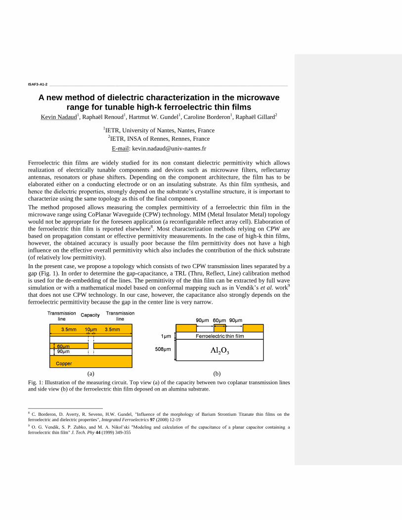
In the present case, we propose a topology which consists of two CPW transmission lines separated by a
gap (Fig. 1). In order to determine the gap-capacitance, a TRL (Thru, Reflect, Line) calibration method
is used for the de-embedding of the lines. The permittivity of the thin film can be extracted by full wave
simulation or with a mathematical model based on conformal mapping such as in Vendik’s et al. work9
that does not use CPW technology. In our case, however, the capacitance also strongly depends on the
ferroelectric permittivity because the gap in the center line is very narrow.
(a) (b)
Fig. 1: Illustration of the measuring circuit. Top view (a) of the capacity between two coplanar transmission lines
and side view (b) of the ferroelectric thin film deposed on an alumina substrate.
8 C. Borderon, D. Averty, R. Seveno, H.W. Gundel, "Influence of the morphology of Barium Strontium Titanate thin films on the
ferroelectric and dielectric properties", Integrated Ferroelectrics 97 (2008) 12-19
9 O. G. Vendik, S. P. Zubko, and M. A. Nikol’ski "Modeling and calculation of the capacitance of a planar capacitor containing a
ferroelectric thin film" J. Tech. Phy 44 (1999) 349-355
ISAF3-A1-3 ____________________________________________________________________________________________________________________
Central mode in perovskite ferroelectrics: terahertz spectroscopy
and molecular dynamics simulations
P. Kužel1, T. Ostapchuk
1, C. Kadlec
1, J. Weerasinghe
2, L. Bellaiche
2 and J. Hlinka
1
1Institute of Physics ASCR, Na Slovance 2, Prague, 182 21, Czech Republic
2Department of Physics, University of Arkansas, Fayetteville, Arkansas 72701, USA
Email: [email protected]
Two limiting cases of structural phase transitions are often distinguished: displacive and order-disorder
types. In the displacive case, the equilibrium positions of atoms or ions in the crystal correspond to their
average positions. The phase transition is triggered by a change of these positions related to the freezing
of a low-frequency phonon mode (called “soft mode”, SM). The order-disorder case involves partially
occupied sites given by the potential minima (disorder) and the transition is connected to the symmetry
breaking of their spatial distribution (ordering): this is connected to an excitation of the relaxation type
(called “central mode”, CM). These excitations are observed by terahertz spectroscopy in ferroelectric
perovskite oxides like (Ba,Sr)TiO3 or K(Ta,Nb)O3 and they often coexist even in the paraelectric phases
and couple to each other10,11
. The complex dielectric function () in the terahertz range then can be
usually described by
/1222
0
2
0
ii, (1)
where 0, 0, are the plasma frequency, oscillator frequency and damping constant of the SM,
respectively; is the bare relaxation frequency of the CM and is the coupling constant.
The experiments can be confronted with molecular dynamics calculations based on an effective
Hamiltonian with parameters derived from first principles. The dynamical degrees of freedom consist of
inhomogeneous and homogeneous strain variables and of so called “local soft modes” corresponding to
local (within a unit cell) displacements of atoms with the SM eigenvector1,12
. These degrees of freedom
are sufficient to explain that in the studied perovskites the CM suddenly appears in the spectra well
above the ferroelectric phase transition. The coexistence of the two spectral features is then an intrinsic
property of these materials and a consequence of a complex anharmonic form of the soft mode effective
potential.
In this contribution we will compare experimental terahertz dielectric spectra on BaxSr1-xTiO3 (BST)
system with molecular dynamics simulations. The temperature trends of the SM and CM behavior are
investigated in the paraelectric phase (T > TC). A transition is observed between high-temperature
spectra (T > TCM) described by a simple damped harmonic oscillator (SM) and a low-temperature
behavior (T < TCM) where the spectra fit to the coupled SM-CM model (1). The CM is understood as a
thermally activated process of hopping between quasi-stable off-center Ti ionic positions described by
Arrhenius-type temperature dependence3. This thermal activation process is at the origin of the change
of the regime between fast and slow relaxation dynamics which then appears almost as a phase transition
in the spectra.
10J. Hlinka et al., Phys. Rev. Lett., vol. 101, 167402, 2008. 11C. Kadlec et al., Phys. Rev. B, vol. 80, 174116, 2009; V. Skoromets et al., Appl. Phys. Lett., vol. 99, 052908, 2011. 12J. Weerasinghe et al., MRS Communications, available online February 2013. doi:10.1557/mrc.2013.5.

ISAF3-A1-4 ____________________________________________________________________________________________________________________
Elastic Anomalies in Ferroelectric Ceramics: Pb(Mg1/3Nb2/3)O3 as
Elastic Relaxor, Octahedral Tilts in Tetragonal Pb(Zr,Ti)O3 and
Magneto-elastic Coupling in BiFeO3
Hana Ursic1,2
, Tadej Rojac1,2
, Li Jin (靳立) 3, Dragan Damjanovic
4
1Electronic Ceramics Department, Jozef Stefan Institute, Ljubljana, Slovenia
2CoE NAMASTE, Ljubljana, Slovenia
3Electronic Materials Research Laboratory, Key Laboratory of the Ministry of Education
& International Center for Dielectric Research, Xi'an Jiaotong University, Xi'an, China 4Ceramics Laboratory, Swiss Federal Institute of Technology in Lausanne - EPFL, Lausanne,
Switzerland
Email: [email protected]
In the large majority of experimental studies the properties of ferroelectrics are examined through
dielectric (polarization-electric field) or piezoelectric (stress/electric field-charge/strain) relations. It is
well known and since a long time, however, that elastic (strain-stress) properties of ferroelectrics may be
very sensitive at low frequencies to structural phase transitions and domain-walls related
processes.i,ii,iii,iv,v,vi
Elastic studies offer complementary information to more common dielectric- and
piezoelectric-oriented investigations and are thus crucial for a better understanding of ferroelectrics.
In this presentation we show results of our recent studies on elastic properties of ferroelectric ceramics.
We employed the dynamic mechanical analyzer technique (DMA), in some cases backed by
piezoelectric resonance measurements, to study several distinct phenomena in ferroelectrics. We
demonstrate that typical relaxor ferroelectric, Pb(Mg1/3Nb2/3)O3, exhibits elastic relaxor behavior, which
we have measured over two orders of magnitude in frequency. That is, Pb(Mg1/3Nb2/3)O3 exhibits what
is today called the “strain glass-like“ behavior.vii
We show evidence of octahedral tilts in two
compositions of tetragonal phase of Pb(Zr1-xTix)O3 (x=0.55 and 58), thus confirming results of earlier
infrared spectroscopy studyviii
and ab-initio calculationsix
. Finally, we give evidence of what appears to
be a strong magneto-elastic coupling in BiFeO3.x
ISAF3-A1-5 ____________________________________________________________________________________________________________________
Ultrasonic determination of anisotropic elasticity of DyScO3
substrates
Hanus Seiner1, Petr Sedlak
1, Michaela Janovska
1, Michal Landa
1,
Pavel Marton2, Petr Ondrejkovic
2 and Jiri Hlinka
2
1Laboratory of Ultrasonic Methods, Institute of Thermomechanics, ASCR,
Praha, Czech Republic 2Department of Dielectrics, Institute of Physics ASCR, Praha, Czech Republic
Email: [email protected]
Rare-earth scandate single crystals have become very popular as substrate materials for the epitaxial growth
of functional thin films, especially in case of ferroelectric and multiferroic perovskite oxides, such as
BiFeO3; EuTiO3; BaTiO3; SrTiO3 or BiMnO3. Hence the elastic constants of the scandates are of high
importance for understanding the behavior of the perovskite films and their further development.
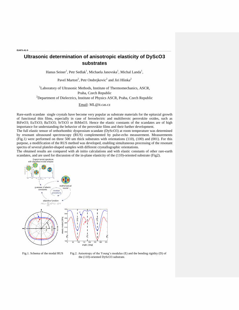
The full elastic tensor of orthorhombic dysprosium scandate (DyScO3) at room temperature was determined
by resonant ultrasound spectroscopy (RUS) complemented by pulse-echo measurement. Measurements
(Fig.1) were performed on three 500 um thick substrates with orientations (110), (100) and (001). For this
purpose, a modification of the RUS method was developed, enabling simultaneous processing of the resonant
spectra of several platelet-shaped samples with different crystallographic orientations.
The obtained results are compared with ab initio calculations and with elastic constants of other rare-earth
scandates, and are used for discussion of the in-plane elasticity of the (110)-oriented substrate (Fig2).
Fig.1. Schema of the modal RUS Fig.2. Anisotropy of the Young’s modulus (E) and the bending rigidity (D) of
the (110)-oriented DyScO3 substrate.

Piezoelectrics
CLUB B
Monday, July 22 2013, 10:30 am - 12:00 pm
Chair: Shujun Zhang
Pennsylvania State University
ISAF2-A2-1 ____________________________________________________________________________________________________________________
Complete Description of Piezoelectric Response
in Fundamental Equations
Takaaki Tsurumi, Manabu Hagiwara, Takuya Hoshina and Hiroaki Takeda
Graduate School of Science and Engineering,
Tokyo Institute of Technology, Meguro, Tokyo, Japan.
Email: [email protected]
Promising applications of piezoelectric ceramics have been changing from devices operated under low
electric fields in electronic circuits to those driven by high electric fields such as actuators for ink-jet
heads, fuel injectors of diesel engines, etc. Under such large-signal operation, response of piezoelectric
ceramics deviates from the conventional linear piezoelectric theory, leading to the appearance of
nonlinear phenomena which causes the unstable operation and heat generation of the devices. Many
researchers have aimed to incorporate the nonlinear and dissipation effects into the piezoelectric theory,
but complete theory of the piezoelectric response have not been established yet. In this study, we will
propose fundamental equations describing the piezoelectric response under the large-signal operation.
The fundamental equations are based on an assumption to simplify the situation: that is piezoelectric e
coefficient is ‘real and constant’. The piezoelectric e coefficient is defined by D = eS, where D and S are
electric displacement and strain, respectively, and D can be regarded as polarization P in piezoelectric
ceramics with high permittivity. Thus, the ‘real and constant’ e coefficient means that S and P have a
linear relationship without a phase lag. This assumption stands to reason, since both S and P are
originated from crystal lattice deformation (intrinsic effect) and non-180○ domain wall motion (extrinsic
effect). From a Taylor series expansion of elastic Gibbs energy considering the assumption, we have
derived the following nonlinear piezoelectric equations in e-form:
3*32*2*1
23*32*2*1
2 EEEESeSD
EeEScScScT
SSS
EEE
,
where T is stress; E is electric field; cE(i)*
is ith-order
elastic stiffness; εS(i)*
is ith-order permittivity; γ is
electrostrictive coefficient. Using the above equations, we
analyzed so-called “jump phenomenon” in piezoelectric
resonator, which is a discontinuous change of current
and/or displacement in piezoelectric resonator at its
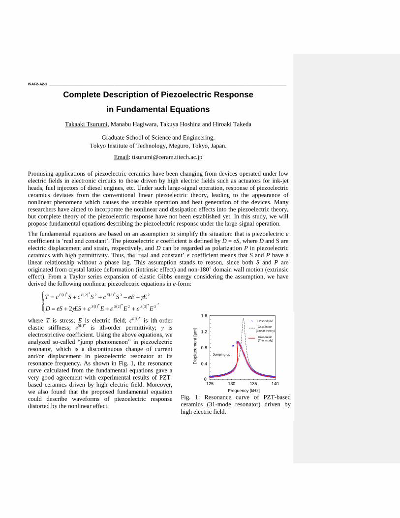
resonance frequency. As shown in Fig. 1, the resonance
curve calculated from the fundamental equations gave a
very good agreement with experimental results of PZT-
based ceramics driven by high electric field. Moreover,
we also found that the proposed fundamental equation
could describe waveforms of piezoelectric response
distorted by the nonlinear effect.
0
0.4
0.8
1.2
1.6
125 130 135 140
Dis
pla
ce
me
nt
[μm
]
Frequency [kHz]
Jumping up
Observation
(This study)
Calculation
(Linear theory)
Calculation
Fig. 1: Resonance curve of PZT-based
ceramics (31-mode resonator) driven by
high electric field.
ISAF2-A2-2 ____________________________________________________________________________________________________________________
Enhanced Large Signal Performance of PZT Thick Film Actuators
for Active Micro-Optics
Dörthe Ernst1, Bernhard Bramlage
1, Sylvia Gebhardt
1, Oliver Pabst
2, Andreas Schönecker
1
1Fraunhofer Institute for Ceramic Technologies and Systems (IKTS), Dresden, Germany
2Fraunhofer Institute for Applied Optics and Precision Engineering (IOF), Jena, Germany
Email: [email protected]
In adaptive optics actuators which allow for high precision positioning with short response time are
needed. More often complex actuator structures which can be individually driven are beneficial.
Piezoceramic thick films offer integrated solutions. By the use of screen printing technology, net-shaped
actuator structures can be directly prepared on wafer-level with high accuracy and reproducibility.
At Fraunhofer IKTS piezoceramic thick films based on lead zirconate titanate (PZT) are available. They
show excellent small and large signal properties. The paper will report on the performance of bending
actuators based on two different PZT compositions. The results lead into the development of complex
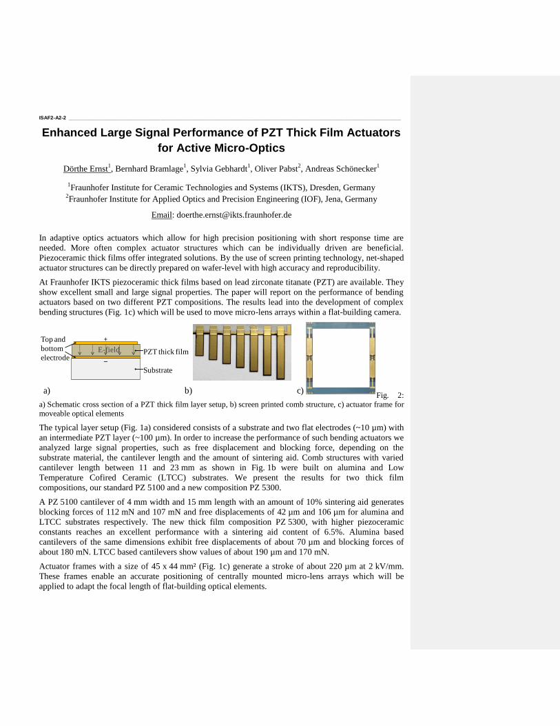
bending structures (Fig. 1c) which will be used to move micro-lens arrays within a flat-building camera.
+
_
E-field
Substrate
Top and
bottom
electrodePZT thick film
a) b) c)Fig. 2:
a) Schematic cross section of a PZT thick film layer setup, b) screen printed comb structure, c) actuator frame for
moveable optical elements
The typical layer setup (Fig. 1a) considered consists of a substrate and two flat electrodes (~10 µm) with
an intermediate PZT layer (~100 µm). In order to increase the performance of such bending actuators we
analyzed large signal properties, such as free displacement and blocking force, depending on the
substrate material, the cantilever length and the amount of sintering aid. Comb structures with varied
cantilever length between 11 and 23 mm as shown in Fig. 1b were built on alumina and Low
Temperature Cofired Ceramic (LTCC) substrates. We present the results for two thick film
compositions, our standard PZ 5100 and a new composition PZ 5300.
A PZ 5100 cantilever of 4 mm width and 15 mm length with an amount of 10% sintering aid generates
blocking forces of 112 mN and 107 mN and free displacements of 42 µm and 106 µm for alumina and
LTCC substrates respectively. The new thick film composition PZ 5300, with higher piezoceramic
constants reaches an excellent performance with a sintering aid content of 6.5%. Alumina based
cantilevers of the same dimensions exhibit free displacements of about 70 µm and blocking forces of
about 180 mN. LTCC based cantilevers show values of about 190 µm and 170 mN.
Actuator frames with a size of 45 x 44 mm² (Fig. 1c) generate a stroke of about 220 µm at 2 kV/mm.
These frames enable an accurate positioning of centrally mounted micro-lens arrays which will be
applied to adapt the focal length of flat-building optical elements.
ISAF2-A2-3 ____________________________________________________________________________________________________________________
Microstereolithography of Piezoelectric Components
David I. Woodward1, Simon J. Leigh
2, Connor Watts
1, Rui Wang
1, Chris Purssell
2, Pam A. Thomas
1,
Duncan R. Billson2
1Department of Physics, University of Warwick, Coventry, UK
2School of Engineering, University of Warwick, Coventry, UK
Email: [email protected]
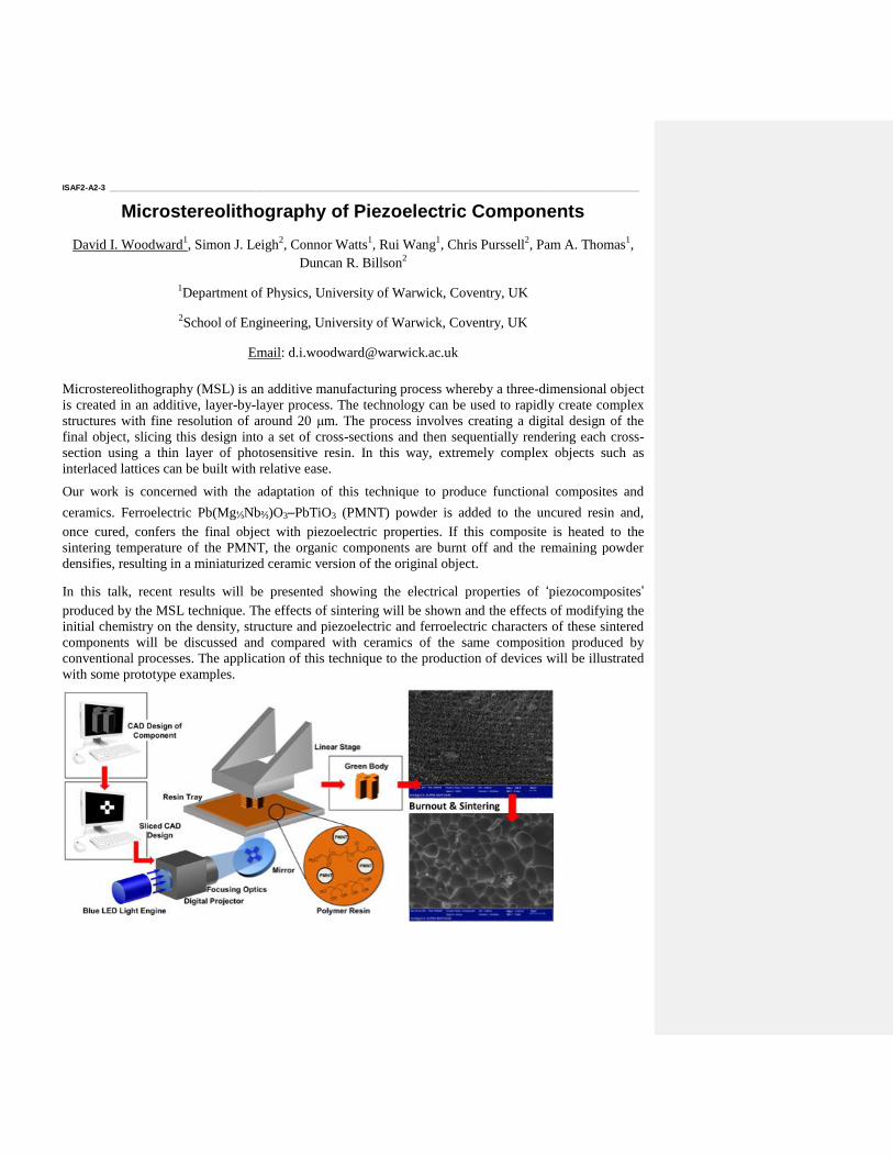
Microstereolithography (MSL) is an additive manufacturing process whereby a three-dimensional object
is created in an additive, layer-by-layer process. The technology can be used to rapidly create complex
structures with fine resolution of around 20 μm. The process involves creating a digital design of the
final object, slicing this design into a set of cross-sections and then sequentially rendering each cross-
section using a thin layer of photosensitive resin. In this way, extremely complex objects such as
interlaced lattices can be built with relative ease.
Our work is concerned with the adaptation of this technique to produce functional composites and
ceramics. Ferroelectric Pb(Mg⅓Nb⅔)O3–PbTiO3 (PMNT) powder is added to the uncured resin and,
once cured, confers the final object with piezoelectric properties. If this composite is heated to the
sintering temperature of the PMNT, the organic components are burnt off and the remaining powder
densifies, resulting in a miniaturized ceramic version of the original object.
In this talk, recent results will be presented showing the electrical properties of ‘piezocomposites’
produced by the MSL technique. The effects of sintering will be shown and the effects of modifying the
initial chemistry on the density, structure and piezoelectric and ferroelectric characters of these sintered
components will be discussed and compared with ceramics of the same composition produced by
conventional processes. The application of this technique to the production of devices will be illustrated
with some prototype examples.
ISAF2-A2-4 ____________________________________________________________________________________________________________________
Fabrication and Electromagnetic Properties of 3D Photonic
Crystals for Microwave Applications
Wei Dai, Hong Wang
Electronic Materials Research Laboratory, Key Laboratory of Ministry of Education,Xi’an Jiaotong
University, Xi’an 710049, China
Email: [email protected]
Photonic crystals (PCs) as a new periodical structure material have inspired great interests of scientists
and industry for their unique, flexible and desirable photonic band gap properties. On the study of the
photonic crystals, it needs to carry out the structure design, in which the main factors influenced the
photonic band gap should be investigated. It needs to master the photonic crystals fabrication process
and investigate the influences of the various defects introduced into the photonic crystals on the
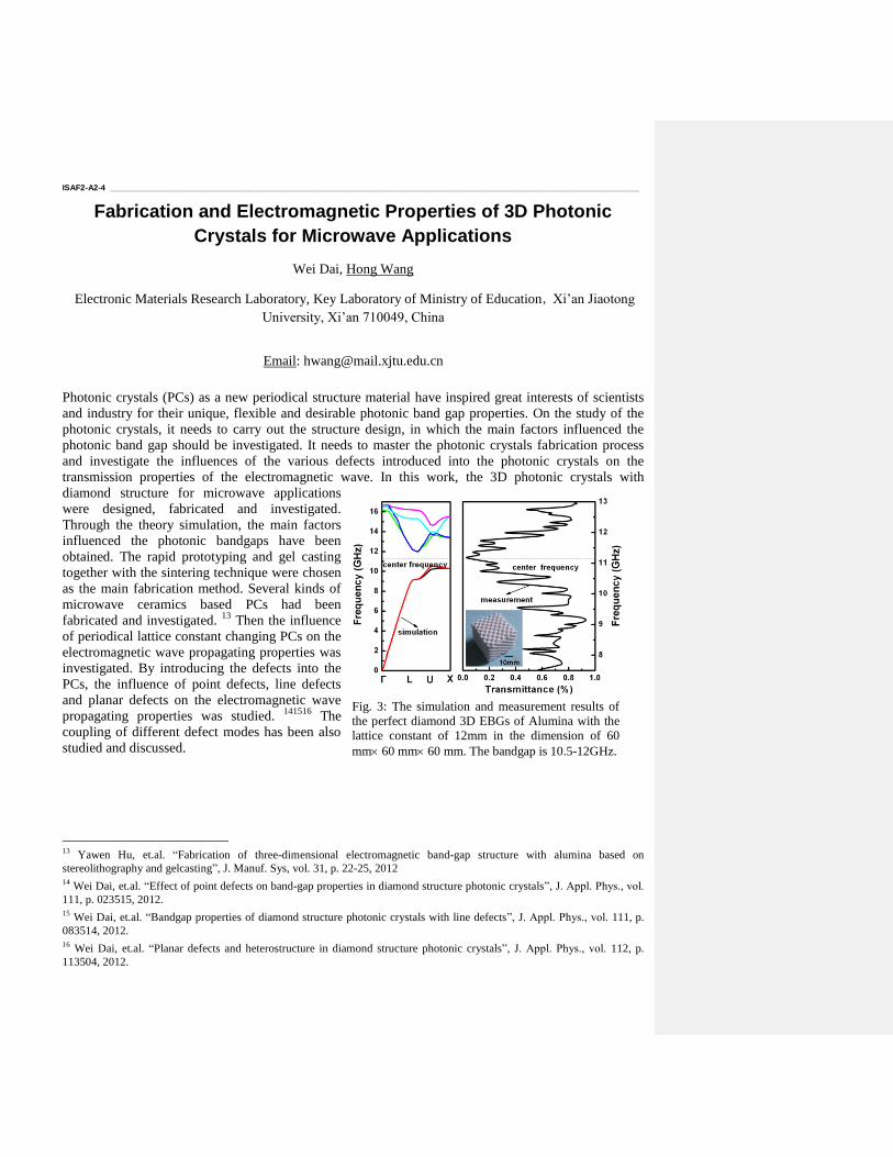
transmission properties of the electromagnetic wave. In this work, the 3D photonic crystals with
diamond structure for microwave applications
were designed, fabricated and investigated.
Through the theory simulation, the main factors
influenced the photonic bandgaps have been
obtained. The rapid prototyping and gel casting
together with the sintering technique were chosen
as the main fabrication method. Several kinds of
microwave ceramics based PCs had been
fabricated and investigated. 13
Then the influence
of periodical lattice constant changing PCs on the
electromagnetic wave propagating properties was
investigated. By introducing the defects into the
PCs, the influence of point defects, line defects
and planar defects on the electromagnetic wave
propagating properties was studied. 141516
The
coupling of different defect modes has been also
studied and discussed.
13
Yawen Hu, et.al. “Fabrication of three-dimensional electromagnetic band-gap structure with alumina based on
stereolithography and gelcasting”, J. Manuf. Sys, vol. 31, p. 22-25, 2012 14
Wei Dai, et.al. “Effect of point defects on band-gap properties in diamond structure photonic crystals”, J. Appl. Phys., vol.
111, p. 023515, 2012. 15
Wei Dai, et.al. “Bandgap properties of diamond structure photonic crystals with line defects”, J. Appl. Phys., vol. 111, p.
083514, 2012. 16
Wei Dai, et.al. “Planar defects and heterostructure in diamond structure photonic crystals”, J. Appl. Phys., vol. 112, p.
113504, 2012.
Fig. 3: The simulation and measurement results of
the perfect diamond 3D EBGs of Alumina with the
lattice constant of 12mm in the dimension of 60
mm 60 mm 60 mm. The bandgap is 10.5-12GHz.
PFM-A3-1 ______________________________________________________________________________________________________________________
Nanoscale Domain Wall Phenomena in Epitaxial Bismuth Ferrite Thin Films
Nagarajan VALANOOR1#+
1School of Materials Science and Engineering, University of New South Wales, Australia
#Corresponding author: [email protected]
+Presenter
In recent years, the control of domains in bismuth ferrite has emerged as a cornerstone of breakthrough science in
multiferroic materials. Domain engineering opens up a vast array of physical phenomena, such as band structure
manipulation, phase transitions and order parameter couplings that are localised at a nanostructured interface, which can then
be harnessed for electronic applications.
This poses a tantalizing new possibility - can the modulation of the physical properties (such as conductance or
magnetoresistance) of the domain wall be controlled by the geometry of the wall itself? In this presentation, we report the
ability to create domain patterns and modulate conduction in domain walls by patterning the domain walls with specific
charge and hence conduction in a multiferroic BiFeO3 thin-film. Domain phase control is achieved by specific SPM based tip
writing. The stability of the phases is rationalized by a phase field model. Secondly by controlling domain wall curvature and
the associated divergence in polarization across the wall, a modulation of consuction is achieved along the domain wall. Both
ambient and Ultra-high Vacuum (UHV) Scanning probe microscopy (SPM) approaches are employed to show that that the
conductivity of the fabricated curved domain walls can be modulated by up to 500% in the spatial dimension. Landau-
Ginzburg-Devonshire computations reveal that the conduction is a result of carriers or vacancies migrating to neutralize the
charge at the formed interface. Polarization dynamics, studied through phase-field models, highlight that anisotropic
conduction may arise from even initially uncharged ring-domain structures. These results offer the first proof of concept for
modulating charge at interfaces in a multiferroic by SPM and further demonstrate that material and electrical parameters can
be extensively controlled at the nanoscale level simply by altering domain geometries. (Vasudevan et al, Nano Letters 2011,
2012)
The presentation is a collaborative effort between the presenting author’s group and groups at Oak Ridge National
Labs, University of Washington, Ukraine National Academy of Sciences and the National Chiao Tung University. The
research at UNSW is supported by the Australian Research Council
PFM-A3-2 ______________________________________________________________________________________________________________________
Thermal quench effects on ferroelectric domain walls
P. Paruch1, A. B. Kolton
2, X. Hong
3,4, C. H. Ahn
3, T. Giamarchi
1
1MaNEP-DPMC, University of Geneva, Geneva, Switzerland
2CONICET, Centro Atomico Bariloche, San Carlos de Bariloche, Argentina
3DAP, Yale University, New Haven, CT, USA
3present address: DPA, University of Nebraksa-Lincoln, Lincoln, NB, USA
Email: [email protected]
Ferroelectric domain walls present a powerful model system for studying the characteristic roughening
and complex dynamics of elastic interfaces in disordered media [1,2]. Although the equilibrium
proerties of such systems are relatively well understood, less is known about their out-of-equilibrium
behavior, and a major challenge is understanding the nonsteady slow dynamics associated with aging
[3]. Experimentally, an interesting realization of such phenomena is provided by quenches, in which a
parameter, such as the temperature of the system, is abruptly varied.
Using piezoresponse force microscopy on epitaxial ferroelectric thin films, we have measured the
evolution of domain wall roughening as a result of such heat-quench cycles up to 735 ◦C, with the
effective roughness exponent ζ changing from 0.25 to 0.5. We discuss two possible mechanisms for the
observed ζ increase: a quench from a thermal one-dimensional configuration and from a locally
equilibrated pinned configuration with a crossover from a two- to one-dimensional regime. We find that
the postquench spatial structure of the metastable states, qualitatively consistent with the existence of a
growing dynamical length scale whose ultraslow evolution is primarily controlled by the defect
configuration and heating process parameters, makes the second scenario more plausible. This
interpretation suggests that pinning is relevant in a wide range of temperatures and, in particular, that
purely thermal domain wall configurations might not be observable in this glassy system.We also
demonstrate the crucial effects of oxygen vacancies in stabilizing domain structures [4].
[1] T. Tybell et al, PRL 89, 097601 (2002)
[2] P. Paruch et al, PRL 94, 197601 (2005)
[3] L. F. Cugliandolo et al, PRL 96, 217203 (2006)
[4] P. Paruch et al, PRB (2012)
PFM-A3-3 ______________________________________________________________________________________________________________________
Disorder and environmental effects on ferroelectric domain wall
dynamics
Jill Guyonnet1, S. Bustingorry
2, C. Blaser
1, E. E. Ferrero
2, I. Gaponenko
1, J. Karthik
3, L. W. Martin
3,
and P. Paruch1
1DPMC, University of Geneva, Switzerland
2CONICET, Centro Atómico Bariloche, San Carlos de Bariloche, Río Negro/Argentina
3Department of Materials Science and Engineering and Materials Research Laboratory, University of
Illinois, Urbana-Champaign, USA
Email: [email protected]
Domain wall motion in ferroelectric materials is largely determined by the disorder pinning potential,
which depends on the nature and density of defects in the sample. Readily controlled with electric fields,
and accessible over a large range of length scales and speeds, the domain walls provide an excellent
model system for the complex fundamental physics of elastic disordered interfaces. Understanding the
microscopic role of defects in domain propagation is also technologically critical in increasingly more
miniaturized devices, scaled down to sizes comparable to the extent of individual defects. In this
context, scanning probe microscopy (SPM) has emerged as a primary technique for domain engineering,
providing a single well-defined nucleation site and nanoscale resolution of the switching dynamics. In
such studies, the highly inhomogeneous electric field produced by the SPM tip can however be
significantly influenced by the presence of adsorbates on the sample surface, resulting in humidity-
dependent domain dynamics [1,2].
Here, we present a systematic study of the interplay between disorder pinning and the screening effects
of surface water on the roughness and switching dynamics of SPM-engineered ferroelectric domains in
Pb(Zr0.2Ti0.8)O3 thin films with different defect densities, in ultrahigh vacuum (UHV) and ambient
conditions. In samples presenting a low, uniform defect density, the switched domains are circular, with
significantly higher growth rates in ambient conditions. In contrast, higher-disorder samples show slow
growth rates in both ambient and UHV, with irregular domain shapes in the latter case. These
experimental observations are in excellent agreement with Ginzburg-Landau numerical simulations of
the localized nucleation and growth of domains under varying disorder and dipolar interaction
magnitudes.
These results show that, while domain growth rates and roughness are governed primarily by disorder,
electrostatic screening by surface water plays an important role, allowing more rapid domain wall
motion in low-disorder samples, and screening the effects of dipolar and disorder forces in high-disorder
samples, which otherwise lead to significant domain wall roughness.
[1] D. Dahan, M. Molotskii, G. Rosenman, and Y. Rosenwaks, Appl. Phys. Lett. 89, 152902 (2006).
[2] V. Ya. Shur, A. V. Ievlev, E. V. Nikolaeva, E. I. Shishkin, and M. M. Neradovskiy, J. Appl. Phys. 110, 052017 (2011).
PFM-A3-4 ______________________________________________________________________________________________________________________
Direct observation of domain wall pinning and creep in
ferroelectric thin film capacitors
Huizhong Zeng, Yao Lei, Wenbo Luo, Wen Huang, Y. Lin
State Key Laboratory of Electronic Thin films and Integrated Devices, University of Electronic Sci. &
Tech. of China, Chengdu, P. R. China
Email: [email protected]
The creep-like motion of ferroelectric domain wall (DW) is crucial to understand the role of defect
pinning. A nanoscale scanning probe study of DW pinning and creep motion was preformed in
ferroelectric thin film capacitors. The ferroelectric capacitors are prepared by pulsed laser deposition of
(Pb0.8Zr0.2)TiO3 (PZT) and SrRuO3 (SRO) electrodes onto SrTiO3 single crystal substrates. The ultra-
thin (<10 nm) SRO top electrode enable piezoresponse force microscope (PFM) to visualize
ferroelectric domains in the capacitors, and provide a homogeneous electric field for studying static and
dynamic DW properties. From the static domain wall profiles, the averaged roughness exponent is
extracted to be ~0.39, indicating a 2D DW in the presence of random bond disorder and long range
dipole interaction. By applying the electric pulses (E ≥ EC) to the capacitors, creep-like DW motion was
directly observed. By measuring the averaged speed of DW, the critical exponent is determined to be
μ=1, confirming the random bond disorder. However, a DW roughening process was observed when
decreasing the pulsed electric field. When further decreasing the pulsed electric field, both creep-like
motion and nucleation of bubbles in front of DW were found, indicating the significant role of defect
pining. The transition from creep motion to the bubble formation was discussed. Our results suggest the
disordered elastic model oversimplified the DW motion under lower field.
Fig. 4: Motion of domain walls of ferroelectric thin
films capacitors under pulsed electric field lower
than EC (left) and larger than EC (right). The DW
position before and after electric pulse is colored by
dark and orange, respectively. The vertical scan
range of PFM is 6 μm.
PFM-A3-5 ______________________________________________________________________________________________________________________
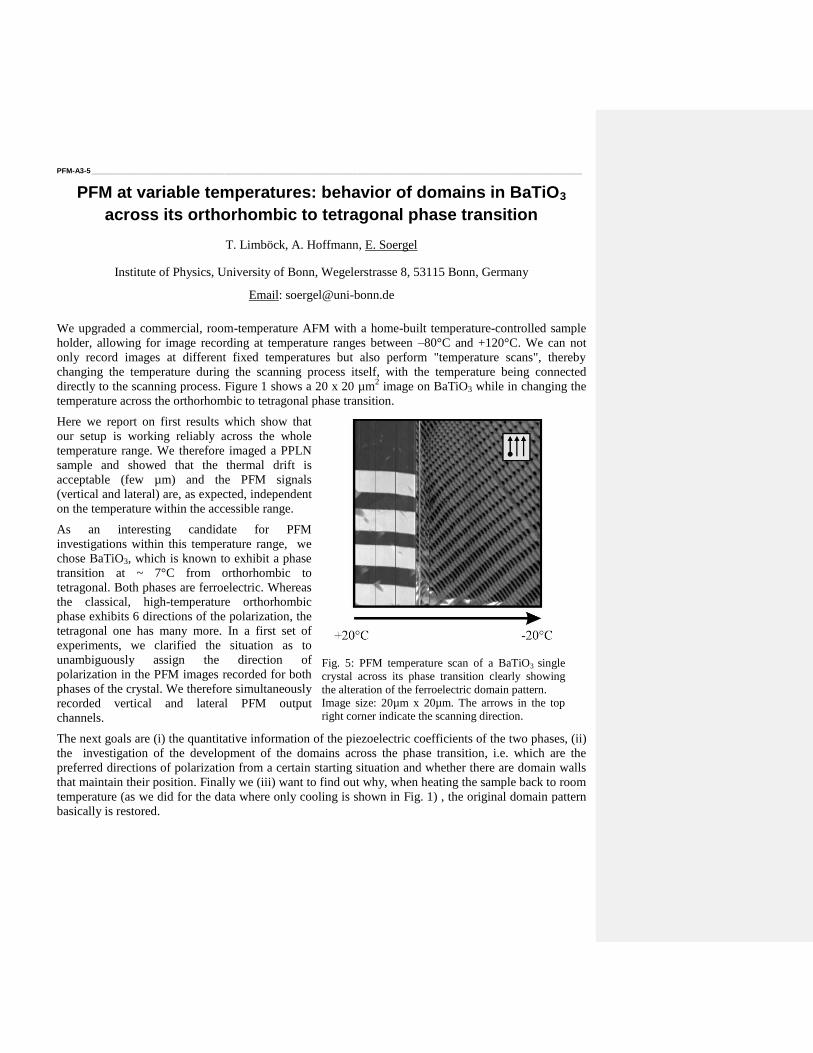
PFM at variable temperatures: behavior of domains in BaTiO3
across its orthorhombic to tetragonal phase transition
T. Limböck, A. Hoffmann, E. Soergel
Institute of Physics, University of Bonn, Wegelerstrasse 8, 53115 Bonn, Germany
Email: [email protected]
We upgraded a commercial, room-temperature AFM with a home-built temperature-controlled sample
holder, allowing for image recording at temperature ranges between –80°C and +120°C. We can not
only record images at different fixed temperatures but also perform "temperature scans", thereby
changing the temperature during the scanning process itself, with the temperature being connected
directly to the scanning process. Figure 1 shows a 20 x 20 µm2 image on BaTiO3 while in changing the
temperature across the orthorhombic to tetragonal phase transition.
Here we report on first results which show that
our setup is working reliably across the whole
temperature range. We therefore imaged a PPLN
sample and showed that the thermal drift is
acceptable (few µm) and the PFM signals
(vertical and lateral) are, as expected, independent
on the temperature within the accessible range.
As an interesting candidate for PFM
investigations within this temperature range, we
chose BaTiO3, which is known to exhibit a phase
transition at ~ 7°C from orthorhombic to
tetragonal. Both phases are ferroelectric. Whereas
the classical, high-temperature orthorhombic
phase exhibits 6 directions of the polarization, the
tetragonal one has many more. In a first set of
experiments, we clarified the situation as to
unambiguously assign the direction of
polarization in the PFM images recorded for both
phases of the crystal. We therefore simultaneously
recorded vertical and lateral PFM output
channels.
The next goals are (i) the quantitative information of the piezoelectric coefficients of the two phases, (ii)
the investigation of the development of the domains across the phase transition, i.e. which are the
preferred directions of polarization from a certain starting situation and whether there are domain walls
that maintain their position. Finally we (iii) want to find out why, when heating the sample back to room
temperature (as we did for the data where only cooling is shown in Fig. 1) , the original domain pattern
basically is restored.
Fig. 5: PFM temperature scan of a BaTiO3 single
crystal across its phase transition clearly showing
the alteration of the ferroelectric domain pattern.
Image size: 20µm x 20µm. The arrows in the top
right corner indicate the scanning direction.

Pb-based ceramics: Spectroscopy
CLUB A
Monday, July 22 2013, 02:00 pm - 03:30 pm
Chair: Jan Petzelt
Institute of Physics ASCR
ISAF3-B1-1 ____________________________________________________________________________________________________________________
Soft mode in cubic PbTiO3 by hyper-Raman scattering
Jiri Hlinka1, Bernard Hehlen
2, Antoni Kania
3, Ivan Gregora
1
1Institute of Physics, Academy of Sciences of the Czech Republic, Prague, Czech Republic
2Laboratoire des Colloides, Verres et Nanomatériaux (LCVN), UMR CNRS 5587, University of
Montpellier II, Montpellier, France 3Institute of Physics, University of Silesia, Katowice, Poland
Email: [email protected]
Terahertz-range frequency dispersion of the dielectric
permittivity provides the key information needed to
understand the potential of practical use of the high
permittivity materials.
Therefore, it seems also important to provide clean
examples of ferroelectric materials where the THz range
permittivity is actually well described by a single polar soft
mode excitation.
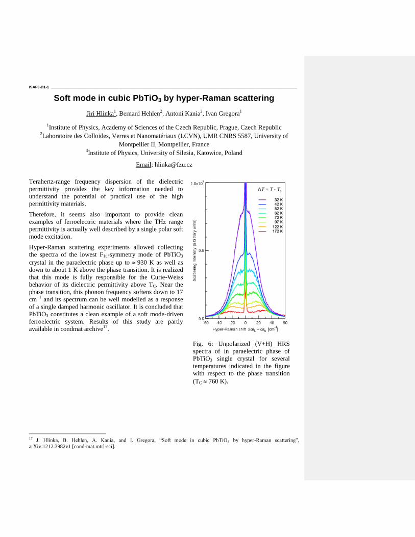
Hyper-Raman scattering experiments allowed collecting
the spectra of the lowest F1u-symmetry mode of PbTiO3
crystal in the paraelectric phase up to 930 K as well as
down to about 1 K above the phase transition. It is realized
that this mode is fully responsible for the Curie-Weiss
behavior of its dielectric permittivity above TC. Near the
phase transition, this phonon frequency softens down to 17
cm−1
and its spectrum can be well modelled as a response
of a single damped harmonic oscillator. It is concluded that
PbTiO3 constitutes a clean example of a soft mode-driven
ferroelectric system. Results of this study are partly
available in condmat archive17
.
17
J. Hlinka, B. Hehlen, A. Kania, and I. Gregora, “Soft mode in cubic PbTiO3 by hyper-Raman scattering”,
arXiv:1212.3982v1 [cond-mat.mtrl-sci].
Fig. 6: Unpolarized (V+H) HRS
spectra of in paraelectric phase of
PbTiO3 single crystal for several
temperatures indicated in the figure
with respect to the phase transition
(TC 760 K).
ISAF3-B1-2 ____________________________________________________________________________________________________________________
Infrared and terahertz spectroscopy of antiferroelectric PbZrO3
single crystals
Tetyana Ostapchuk1, Christelle Kadlec
1, Petr Kužel
1, Jan Kroupa
1,
Vladimír Železný1, Jan Petzelt
1, Jiří Hlinka
1, and Jan Dec
2
1Department of Dielectrics, Institute of Physics, 18221 Prague 8, Czech Republic
2Institute of Materials Science, University of Silesia, Bankowa 12, PL-40-007 Katowice, Poland
Email: [email protected]
Here, for the first time, we present dielectric dispersion spectra of monodomain PbZrO3 single crystals
obtained along all three orthorhombic axes from far infrared reflectivity and time-domain terahertz
transmission measurements in the 10-500 K temperature range. Within this study we identified the
whole set of the modes, predicted by the factor-group analysis for Pbam structure (11 B1u(z), 17 B2u(y)
and 17 B3u(x)). As typical for all Pb-based perovskites, the spectra exhibit three main bands with the
lowest one corresponding to the Last-type vibrations, the middle (of the largest mode plasma frequency)
to the Slater-type, and the highest one - to the Axe-type vibrationsxi
. The Last-type band of B2u(y)-
symmetry demonstrates a significant coupling to the Slater-type band at low temperatures, which
gradually vanishes on heating, while in the case of B1u(z) symmetry this coupling is less pronounced and
for the B3u(x) symmetry practically negligible.
The softening of the lowest Last-type band is observed in all three normal-axes directions, but the
largest effect (from ~ 75 cm-1
at T=10 K to ~30 cm-1
at T=500 K) is found along the [001] direction
(B1u(z) symmetry), which was suggested to be polar (but not ferroelectric) in the earliest structural
studyxii
. In this direction we have also discerned a weak central-mode (CM) type dispersion around 0.3
THz, analogous to the previously observed on the multidomain crystalxiii
and ceramicsxiv
. Its behavior is
rather similar to that found in BaTiO3 in the [001] direction of the spontaneous polarizationxv
, but its
dielectric strength is several times weaker. In the same sub-THz frequency range in B2u(y)-symmetry
spectra we observed a slightly stronger dispersion, which preserves in the terahertz spectra down to the
lowest temperatures, and assigned it to a pseudophason response.
ISAF3-B1-3 ____________________________________________________________________________________________________________________
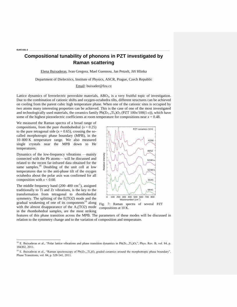
Compositional tunability of phonons in PZT investigated by
Raman scattering
Elena Buixaderas, Ivan Gregora, Mael Guennou, Jan Petzelt, Jiří Hlinka
Department of Dielectrics, Institute of Physics, ASCR, Prague, Czech Republic
Email: [email protected]
Lattice dynamics of ferroelectric perovskite materials, ABO3, is a very fruitful topic of investigation.
Due to the combination of cationic shifts and oxygen-octahedra tilts, different structures can be achieved
on cooling from the parent cubic high temperature phase. When one of the cationic sites is occupied by
two atoms many interesting properties can be achieved. This is the case of one of the most investigated
and technologically used materials, the ceramics family Pb(Zr1-xTix)O3 (PZT 100x/100(1-x)), which have
some of the highest piezoelectric coefficients at room temperature for compositions near x = 0.48.
We measured the Raman spectra of a broad range of
compositions, from the pure rhombohedral (x = 0.25)
to the pure tetragonal side (x = 0.65), crossing the so-
called morphotropic phase boundary (MPB), in the
10–800 K temperature range. We also measured
single crystals near the MPB down to He
temperatures.
Dynamics of the low-frequency vibrations —mainly
connected with the Pb atoms— will be discussed and
related to the recent far-infrared data obtained for the
same samples.18
Doubling of the unit cell at low
temperatures due to the anti-phase tilt of the oxygen
octahedra about the polar axis was confirmed for all
composition with x < 0.60.
The middle frequency band (200–400 cm-1
), assigned
traditionally to Ti and Zr vibrations, is the key to the
transformation from tetragonal to rhombohedral
symmetry. The splitting of the E(TO2) mode and the
gradual weakening of one of its components19
along
with the almost disappearance of the A1(TO2) mode
in the rhombohedral samples, are the most striking
features of this phase transition across the MPB. The parameters of these modes will be discussed in
relation to the symmetry change and to the variation of composition and temperature.
18
E. Buixaderas et al., “Polar lattice vibrations and phase transition dynamics in Pb(Zr1-xTix)O3”, Phys. Rev. B, vol. 84, p.
184302, 2011. 19
E. Buixaderas et al., “Raman spectroscopy of Pb(Zr1-xTix)O3 graded ceramics around the morphotropic phase boundary”,
Phase Transitions, vol. 84, p. 528-541, 2011.
0 100 200 300 400 500 600 700 800
58/42
42/58
55/45
52/48 b
52/48 a
PZT ceramics 10 K
Re
lative
in
ten
sity
Wavenumber (cm-1)
48/52
Fig. 7: Raman spectra of several PZT
compositions at 10 K.
ISAF3-B1-4 ____________________________________________________________________________________________________________________
PbZrO3: nature of the high temperature phase transition R. Faye1, H. Liu1, D. Kajewski
2, K. Roleder
2, P. Gemeiner1, B. Dkhil1, and P.-E. Janolin1
1SPMS laboratory, UMR CNRS-Ecole Centrale Paris, Chatenay-Malabry, France
2Institute of Physics, University of Silesia,Katowice, Poland
Email: [email protected]
Despite being the archetypal antiferroelectric perovskite the comprehension of lead zirconate (PZO)
structure and phase transition(s) is still fragmentary. PZO structure remained elusive between the 50's
when its antiferroelectricity was discovered by Shirane20 and the results of first principles calculations
circa 200021. Since then, the description of the AFE phase by a nonpolar Pbam orthogonal space group
has been preferred over the polar Pba2 one. Nevertheless a controversy persists over the nature of the
high temperature phase transition and the existence of an intermediate stable FE phase22. As a
consequence, the structure-property relation has so far not been comprehensively established.
We shall aim at providing insights on these points through temperature dependent X-ray diffraction,
neutron scattering, Raman spectroscopy, dielectric, pyroelectric, differential scanning calorimetry, and
hysteresis loop measurements performed on ceramics and single crystals. The effect of heat, density,
time and particle sizes on the FE zone will be considered. In addition, we shall report the results of
temperature-dependent X-ray diffraction with in-situ AC electric field.
20
G.Shirane,E. Sawaguchi, “Dielectric properties of lead zirconate”, Phys. Rev. 84,476 (1951)
21 D.J. Singh, “Structure and energetic of antiferroelectric PbZrO3”, Phys. Rev. B 52, 12559 (1995)
22 K. Roleder et al. “The first evidence of two phase transitions in PbZrO3 crystals derived from simultaneous
Raman and dielectric measurement”, Ferroelectrics 80, 161 (1988)
ISAF3-B1-5 ____________________________________________________________________________________________________________________
Study of ferroelectric-antiferroelectric crossover in PLZT (x/90/10)
ceramics
L. Curecheriu1
, L. Stoleriu1, C. Galassi
2, F. Fochi
2, L. Mitoseriu
1
1 Faculty of Physics, Al. I. Cuza Univ., Bv. Carol I no. 11, Iasi 700506, Romania
2 ISTEC-CNR, Via Granarolo no. 64, I-48018 Faenza, Italy
Email: [email protected]
(Pb1-xLax)(Zr0.90Ti0.10)1-x/4O3 [PLZT x/90/10 with compositions: x=0.0, 2.0, 2.5, 3.0, 3.5, 3.8 and
4.0] solid solutions have been prepared by solid state reaction and sintering at 12500C/2h. The phase
purity, crystalline symmetry and microstructures have been investigated. Dense ceramics (relative
density above 95-98%) and homogeneous microstructures have been obtained for all the compositions.
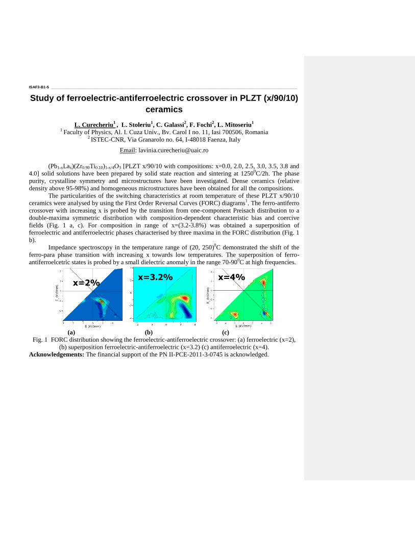
The particularities of the switching characteristics at room temperature of these PLZT x/90/10
ceramics were analysed by using the First Order Reversal Curves (FORC) diagrams1. The ferro-antiferro
crossover with increasing x is probed by the transition from one-component Preisach distribution to a
double-maxima symmetric distribution with composition-dependent characteristic bias and coercive
fields (Fig. 1 a, c). For composition in range of x=(3.2-3.8%) was obtained a superposition of
ferroelectric and antiferroelectric phases characterised by three maxima in the FORC distribution (Fig. 1
b).
Impedance spectroscopy in the temperature range of (20, 250)0C demonstrated the shift of the
ferro-para phase transition with increasing x towards low temperatures. The superposition of ferro-
antiferroelcetric states is probed by a small dielectric anomaly in the range 70-900C at high frequencies.
(a) (b) (c)
Fig. 1 FORC distribution showing the ferroelectric-antiferroelectric crossover: (a) ferroelectric (x=2),
(b) superposition ferroelectric-antiferroelectric (x=3.2) (c) antiferroelectric (x=4).
Acknowledgements: The financial support of the PN II-PCE-2011-3-0745 is acknowledged.
x=4% x=3.2% x=2%
ISAF3-B1-6 ____________________________________________________________________________________________________________________
Microwave dielectric properties of relaxor ferroelectric
Pb(In1/2Nb1/2)O3-Pb(Mg1/3Nb2/3)O3-PbTiO3 single crystals
Li Jin1, Fei Li
1, Shujun Zhang
2, Dragan Damjanovic
3
1Electronic Materials Research Laboratory, Key Laboratory of the Ministry of Education & International
Center for Dielectric Research, Xi’an Jiaotong University, Xi’an, China 2Materials Research Institute, Pennsylvania State University, University Park, Pennsylvania, USA
3Ceramics Laboratory, Swiss Federal Institute of Technology in Lausanne - EPFL, Lausanne,
Switzerland
Email: [email protected]
Relaxor ferroelectric single crystals with the composition near the morphotropic phase boundary (MPB)
region have attracted much attention due to their superior piezoelectric and dielectric properties. Up to
date, the routine piezoelectric, dielectric and elastic properties of relaxor ferroelectric single crystals
have been studied. Many representative opinions based on intrinsic crystal lattice and extrinsic domain
wall motion have been proposed to understand high properties. However, their origin is still under
debate.23,24
Ferroelectric materials show strong dielectric dispersion in GHz frequency range, which manifests itself
as the rapid decrease of the permittivity with increasing the frequency and accompanied with a loss
peak.25,26,
This phenomenon is mainly attributed to the domain wall motion and piezoelectric grain
resonance.27
By means of this dielectric dispersion, we could distinguish the intrinsic and extrinsic
contribution to the dielectric properties.28
In this presentation, we show results on microwave dielectric
properties of relaxor ferroelectric Pb(In1/2Nb1/2)O3-Pb(Mg1/3Nb2/3)O3-PbTiO3 (PIN-PMN-PT) single
crystals. The dielectric response was studied from 100 kHz to 1.8 GHz at temperatures from -100 to 100 oC. By changing the domain wall density through by gradually depoling samples, we evaluated the
domain wall motion contribution to the dielectric properties. A dispersion-free state at GHz range for
single domain state was observed, where the value ( 160 ) measured at 1.8 GHz accounts for the
intrinsic dielectric response of PIN-PMN-PT single crystals.
23
D. Damjanovic, IEEE Trans. Ultrason. Ferroelectr. Freq. Control 56, 1574 (2009). 24
S. Zhang and F. Li, J. Appl. Phys. 111, 031301 (2012). 25
G. Arlt, U. Böttger, and S. Witte, Ann. Phys. 506, 578 (1994). 26
M. P. McNeal, S. J. Jang, and R. E. Newnham, J. Appl. Phys. 83, 3288 (1998). 27
V. Porokhonskyy, L. Jin, and D. Damjanovic, Appl. Phys. Lett. 94, 212906 (2009). 28
L. Jin, V. Porokhonskyy, and D. Damjanovic, Appl. Phys. Lett. 96, 242902 (2010).

Relaxor Materials
CLUB B
Monday, July 22 2013, 02:00 pm - 03:30 pm
Chair: Takaaki Tsurumi
Tokyo Institute of Technology
ISAF1-B2-1 ____________________________________________________________________________________________________________________
Similarities between the physic of relaxors and other systems
S. Prosandeev1,2
, B. Dkhil3
1Department of Physics, Research Institute of Physics,
Southern Federal University, Rostov on Don 344090, Russia 2Physics Department and Institute for Nanoscience and Engineering,
University of Arkansas, Fayetteville, AR 72701, USA 3Ecole Centrale Paris/CNRS UMR8580, Chatenay-Malabry, France
Email: [email protected]
In this presentation, the main idea is to demonstrate that relaxors share common features with many
other systems; these features being related to various and exotic phenomena like the weak crystallization
in lipids, the Bose condensation in Helium II state or the pseudo-gap in superconductors. The tempting
proximity of these phenomena will be discussed and used to propose a unified microscopic picture of
relaxors. As a matter of fact, two new order parameters will be introduced to characterize the transitions
occurring at Burns temperature and that at T* which marks the crossover between a spherical glass and a
quadrupole glass state.
ISAF1-B2-2 ____________________________________________________________________________________________________________________
Temperature Evolution of Dielectric Relaxation in PMN Single
Crystals
Viktor Bovtun, Stanislav Kamba, Jan Petzelt, Jiri Hlinka
Department of Dielectrics, Institute of Physics ASCR, Prague, Czech Republic
Email: [email protected]
Dielectric relaxation in PbMg1/3Nb2/3O3 (PMN) was widely studied since 1960. It is observed in broad
frequency and temperature ranges, slows down and broadens on cooling, partially freezes out below the
freezing temperature Tf ≈ 200 K and is characterized by the extremely broad distribution of relaxation
times below Tf. Here we present a detailed analysis of the relaxation based on the complete dielectric
spectra from 3 mHz to 3 THz,which joined our experimental results
29-6. Asymmetrical shape the of loss
spectra ′′(log f) indicates the presence of at least two relaxation contributions which are diffuse and
overlapped. The Cole-Cole fit allows separation of two contributions (subscripts “1” and “2”) and
evaluation of their parameters: dielectric strength, mean relaxation time 0, relaxation time distribution
(RTD) parameter.
Using the uniform RTD function7, upper (U) and lower (L) limits of RTD were determined for both
Cole-Cole contributions. Temperature dependences of 02 and L2 can be fitted to the Arrhenius law,
while that of 01 and U1 fit well to the Vogel-Fulcher law above 220 K. The longer mean relaxation time
01 does not diverge at Tf and remains finite even below Tf. We attribute this to the crossover from
Vogel-Fulcher to Arrhenius behavior.
As a result of the analysis, we obtained a time-temperature diagram of dielectric relaxation in PMN.
According to the diagram, the relaxation dynamics covers a time range limited by the longest relaxation
time U1 diverging on cooling according to the Vogel-Fulcher law (or et least approaching the Ts range
at Tf) and shortest relaxation timeL2 following the Arrhenius law with a small activation energy (i.e.
week temperature dependent in the ps range).
The described evolution of relaxation dynamics corresponds well to the general scheme of dielectric
response of relaxor ferroelectrics1,8
based on the concept of polar nanoclusters (or nanoregions) whose
flipping and breathing provide two relaxation contributions. The relation of the relaxation dynamics to
the concepts of ferroelectric nanodomains9 or ion chemistry and environment (based on molecular
dynamics simulations10
) is under discussion.
29 V. Bovtun, S. Veljko, S. Kamba, J. Petzelt, S. Vakhrushev, et al. - J. Europ. Cer. Soc. 26, 2867-2875, 2006.
2 V.P. Bovtun, N.N. Krainik, L.A. Markova, Y.M. Poplavko, et al. – Fiz. Tverd. Tela 26, 378 – 381, 1984.
3 Y.M. Poplavko, V.P. Bovtun, N.N. Krainik, G.A. Smolensky – Fiz. Tverd. Tela 25, 1263-1265, 1985.
4 E.V.Colla, E.Y. Koroleva, N.M. Okuneva, S.B Vakhrushev - J. Phys.: Cond. Matter 4, 3671–3677, 1992.
5 V.P. Bovtoun, M.A. Leshchenko - Ferroelectrics 190, 185-190, 1997.
6 V. Bovtun, S. Kamba, A. Pashkin, M. Savinov, P. Samoukhina, et al. – Ferroelectrics 298, 23-30, 2004.
7 S. Kamba, V. Bovtun, J. Petzelt, I. Rychetsky, et al.- J. Phys.: Cond. Matter 12, 497–519, 2000.
8 V. Bovtun, J. Petzelt, V. Porokhonskyy, S. Kamba, et al. – J. Europ. Ceram. Soc. 21, 1307-1311, 2001.
9 J. Hlinka – J. Adv. Dielectrics 2, 1241006, 2012.
10 I. Grinberg, Y.H. Shin, A.M. Rappe – Phys. Rev. Lett. 103, 197601, 2009.
ISAF1-B2-3 ____________________________________________________________________________________________________________________
Acoustic evidence of distinctive temperatures in relaxor-multiferroics
E.Smirnova1, A.Sotnikov
1,2, S.Ktitorov
3, H.Schmidt
2, M.Weihnacht
2
1 Department of Ferroelectricity, A.F.Ioffe Physical-Technical Institute, St. Petersburg, Russia,
2 Department of Magnetic and Acoustic Resonances, IFW Dresden, Dresden, Germany, 3
Department of semiconductors and dielectrics theory, A.F.Ioffe Physical-Technical Institute, St.
Petersburg, Russia
E-mail: [email protected]
Structurally disordered perovskites - relaxor ferroelectrics with magnetic ordering (relaxor-
multiferroics) occupy a special place in the multiferroics family. Coexistence of the relaxor ferroelectric
and magnetic subsystems determines their physical properties. The origin of the relaxor state is still
controversial in spite of the long time experimental and theoretical studies. The first and very famous
approach assumes that unique properties of relaxor ferroelectrics are due to the presence of polar
nanoregions (PNR). Some experimental evidences of the creation of PNR in the paraelectric matrix of
relaxors around so-called Burns temperature (TB) were obtained from the measurements of the optical
refraction index, thermal capacity, and neutron scattering. Scarce results demonstrate acoustic emission
signals and small elastic anomalies in the vicinity of TB. It is well known that acoustic wave velocity
and attenuation are very sensitive to various processes related to phase transitions, relaxations, glass-like
behavior, etc. Recently, we have reported that peaks of acoustic attenuation at TB and T*(temperature of
assumed nanoscale phase transition due to random field) are revealed in classic relaxor PbMg1/3Nb2/3O3
(PMN) and relaxor-multiferroic PbFe1/2Nb1/2O3 (PFN) [1]. The present study is devoted to dielectric and
acoustic properties of relaxors with magnetic ordering PbFe1/2Ta1/2O3 (PFT) and PbFe2/3W1/3O3 (PFW)
in the temperature range from 100 to 700 K. The samples were prepared by a conventional ceramic
technique. Longitudinal ultrasonic wave velocity and attenuation as a function of temperature were
determined by ultrasonic pulse-echo method at frequencies of 5 and 10 MHz (PFT) and 10 MHz (PFW).
Peaks of attenuation in the vicinity of the dielectric constant maximum temperature Tm, suggested Burns
temperature TB and specific temperature T* are found for PFT, as well as for PFW.
The results are discussed on the base of PNR model and on the classical idea by Mandelshtam and
Leontovich of the slowly relaxing internal parameter. This method being applied to the sound
propagation and attenuation problem allows us to describe the acoustic anomaly in the vicinity of Burns
temperature. Slowed-down relaxation in the PNRs leads to an incomplete equilibrium of the system,
and, therefore, to the energy dissipation. PNRs are considered as randomly distributed short-range
relaxing centers interacting with the long-wave acoustic waves. Polarization located in PNR plays a role
of such relaxing parameter. PNR are assumed to have a shape of the ellipsoid; the aspect ratio of it
determines a relative effectiveness of the polarization interaction with the longitudinal and transverse
acoustic waves. Comparison of the results of averaging of the dielectric and acoustic parameters over the
PNR’s configurations with experimental data gives a possibility to estimate the most probable aspect
ratio of the PNR.
1 E.Smirnova, S.Ktitorov , A.Sotnikov, H.Schmidt, M.Weihnacht, “ High Temperature Acoustic Effects
in Relaxors PbMg1/3Nb2/3O3 and PbFe1/2Nb1/2O3”, Proceedings ISAF/ECAPD/PFM 2012,
#6297789, 2012
ISAF1-B2-4 ____________________________________________________________________________________________________________________
Relaxation of Polarized State Created
by Local Electric Field in SBN Single Crystals
Shikhova Vera1, Shur Vladimir
1, Shvartsman Vladimir
2, Lupascu Doru
2, Ievlev Anton
1,
Neradovskiy Maxim1, Pelegov Dmitry
1, Lebedev Vasily
3, Ivleva Lyudmila
4, Dec Jan
5
1Feroelectric laboratory, Ural Federal University, Ekaterinburg, Russia
2Institute for Materials Science, University of Duisburg-Essen, Essen, Germany
3Faculty of Materials Science, Moscow State University, Moscow, Russia
4General Physics Institute of the Russian Academy of Sciences, Moscow, Russia
5Institute of Materials Science, University of Silesia, Katowice, Poland
Email: [email protected]
The temperature and temporal relaxation of the polarized state created by application of the local electric
field using conductive tip of the scanning probe microscope was investigated in pure and doped by Ce
single crystals of relaxor ferroelectric SrxBa1-xNb2O6 (SBN) with x = 0.61 and 0.75.
The 0.5-mm-thick plates of SBN single crystals were cut normally to the polar axis and carefully
polished. The samples before measurements were treated by two alternative procedures:
(1) thermal depolarization (creation of the multi-domain state) by heating up to 200OC and zero-field
cooling, (2) creation of the single domain state by application of 30–50 bipolar triangular or rectangular
field pulses with amplitude and duration sufficient for complete polarization reversal at room
temperature using liquid electrodes.
The polarized areas were created under the action of local electric field of both directions with amplitude
ranged from 40 to 100 V and duration from 1 ms to 1 s at room temperature and at elevated temperature
up to 100OC (above freezing temperature for all compositions). The difference between piezoelectric
responses in the polarized areas produced by application of the field of opposite sign (“contrast”) has
been obtained. The temporal relaxation of the contrast value has been measured at various temperatures.
It was shown that increasing of the field amplitude and pulse duration leads to higher stability of the
polarized state (increasing of the relaxation time constant). The polarized state created in the crystals in
the single domain state was remarkably more stable than in the crystals in the multi-domain state.
Moreover it has been shown that the diameter of the area created at elevated temperatures decreasing
with increasing the temperature. The average value of the induced contrast decreased gradually during
heating and with the increase of the creation temperature for all investigated crystals.
The obtained effects have been attributed to field induced partial polarization of the multidomain state
and important role of the backswitching under the action of depolarization field leading to relaxation of
the piezoresponse value. The acceleration of backswitching at the temperatures above freezing point has
been attributed to additional input of the phase boundaries.
The equipment of the UCSU “Modern Nanotechnology”, Institute of Natural Sciences, UrFU has been
used. The research was made possible in part by RFBR (Grants 13-02-01391-а, 11-02-91066-CNRS-а,
12-02-31377); by Ministry of Education and Science (Contracts 14.513.12.0006, 16.740.11.0585), by
OPTEC LLC and UrFU development program.
ISAF1-B2-5 ____________________________________________________________________________________________________________________
Structural Origins of Strain and Fatigue in 94%(Bi1/2Na1/2)TiO3-
6%BaTiO3
Hugh Simons1, John E. Daniels
2, Julia Glaum
2, Jacob L. Jones
3, Andrew J. Studer
4, Mark Hoffman
2
1Department of Physics, Technical University of Denmark, Lyngby 2800, Denmark
2School of Materials Science & Engineering, University of New South Wales, Sydney, NSW 2052, Australia
3Department of Materials Science & Engineering, University of Florida, Gainesville, FL 32611, USA
4Bragg Institute, Australian Nuclear Science & Technology Organisation, Kirrawee, NSW 2234, Australia
Email: [email protected]
94%(Bi1/2Na1/2)TiO3-6%BaTiO3 (BNT-6BT) remains one of the most intensively studied lead-free
ferroelectric composition for high-strain applications30
. At elevated temperatures (T>75°C), large
recoverable strains (Smax~0.4%) can be attained with low hysteretic loss, accompanied by a reversible
electric-field-induced relaxor-to-ferroelectric transition. However, its ultimate applicability is hindered
by uncertainties regarding the role of this structural transformation on the strain mechanism and fatigue
life. Here, we describe the temperature-dependence of this transition from 25˚C to 100˚C, and its
influence on the macroscopic strain and fatigue.
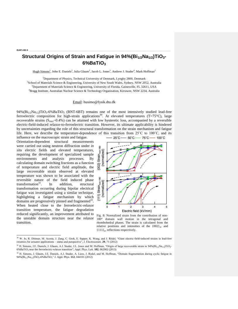
Orientation-dependent structural measurements
were carried out using neutron diffraction under in
situ electric fields and elevated temperatures,
requiring the development of specialized sample
environments and analysis processes. By
calculating domain switching fractions as a function
of temperature and electric field amplitude, the
large recoverable strain observed at elevated
temperature was shown to be associated with the
reversible nature of the field induced phase
transformation31
. In addition, structural
transformation occurring during bipolar electrical
fatigue was investigated using a similar technique,
highlighting a fatigue mechanism by which
domains are progressively pinned and fragmented32
.
When heated close to the ferroelectric-relaxor
transition temperature, the fatigue degradation
reduced significantly, an improvement attributed to
the unstable domain structure near the relaxor
transition.
30 W. Jo, R. Dittmer, M. Acosta, J. Zang, C. Groh, E. Sapper, K. Wang, and J. Rödel, “Giant electric-field-induced strains in lead-free
ceramics for actuator applications – status and perspective”, J. Electroceram. 29, 71 (2012)
31 H. Simons, J.E. Daniels, J. Glaum, A.J. Studer, J.L. Jones and M. Hoffman, “Origin of large recoverable strain in 94%(Bi1/2Na1/2)TiO3-
6%BaTiO3 near the ferroelectric-relaxor transition”, Appl. Phys. Lett. 102, 062902 (2013)
32 H. Simons, J. Glaum, J.E. Daniels, A.J. Studer, A. Liess, J. Rodel, and M. Hoffman, “Domain fragmentation during cyclic fatigue in
94%(Bi1/2Na1/2)TiO3-6%BaTiO3” J. Appl. Phys. 112, 044101 (2012)
Fig. 8: Normalized strain from the contribution of non-
180° domain wall motion in the tetragonal and
rhombohedral phases. The strain is calculated from the
relative positions and intensities of the {002}pc and
{111}pc reflections respectively.
ISAF1-B2-6 ____________________________________________________________________________________________________________________
Julia Glaum1, Hugh Simons
1,3,4, Mark Hoffman
1
Matias Acosta2
1 School of Materials Science and Engineering, University of New South Wales, NSW 2052, Australia
2 Institute of Materials Science, Ceramics Group, Technische Universität Darmstadt, Germany
3 School of Physics, Technical University of Denmark, Lyngby, Denmark
4 European Synchrotron Radiation Facility, Grenoble 38000, France
Temperature-dependency of the relaxor-ferroelectric transition in BNT-BZT ceramics
Piezoelectric ceramics are used in a wide range of actuating applications, utilizing their characteristic to
transform electrical power into mechanical strain. In pure ferroelectric compositions the strain
mechanism is based on the reorientation of ferroelectric domains and the intrinsic elongation of the unit
cells along the direction of the applied field. However, in relaxor-type ceramics a third mechanism can
contribute to the strain. It is based on an electric-field-induced transformation between the
macroscopically non-polar relaxor state and the polar ferroelectric state and the associated high degree
of domain alignment. In these materials the maximum unipolar strain is achieved at temperatures close
to the transition temperature TF-R where the ferroelectric state becomes unstable in the absence of an
external electric field.
One of the most promising lead-free piezoelectric systems is (Bi1/2Na1/2)TiO3-6BaTiO3 (BNT-6BT) with
electromechanical properties similar to the widely used Pb(Zr,Ti)O3 system. It exhibits relaxor
characteristics and a ferroelectric state can be induced by electric field application. The transition
temperature for BNT-6BT ceramics appears to be around 80°C. Doping with small amounts of Zr was
found to increase the maximum strain, which makes this modification of BNT-BT interesting for high-
strain applications.
This study investigates the influence of Zr-doping on the electric field induced relaxor-ferroelectric
transition of the system BNT-6BT. Zr addition leads to a de-stabilization of the induced ferroelectric
order, resulting in a lower transition temperature TF-R and a corresponding increase in unipolar strain.
However, the electric field E* needed to induce this transition appears to be only slightly temperature
dependent. Temperature dependent polarization and permittivity measurements will be utilized to
explore the temperature-electric field diagram.

PFM2
CLUB C
Monday, July 22 2013, 02:00 pm - 03:30 pm
Chair: To Be Announced
PFM-B3-1 ______________________________________________________________________________________________________________________
Electrical Modulation of the Local Conduction at BiFeO3-CoFe2O4
Tubular Oxide Interface
Ying-Hao Chu
Department of Materials Science and Engineering, National Chiao Tung University, Hsinchu, Taiwan
30010, R.O.C.
Email: [email protected]
Complex oxide interfaces emerge as one of the most exciting subjects among condensed matters due to
their unique physical properties and new possibilities for next-generation electronic devices. Three types
of complex oxide interfaces have been established. Among them, the most explored interface is the
artificially constructed heterointerfaces. Various interactions at the interface have resulted in a number
of exciting discoveries, such as highly mobile quasi-
two dimensional electron gas (2DEG) forms between
two band insulators (LaAlO3 and SrTiO3). Moreover,
in ferroic oxides, domain walls dictate natural homo-
interfaces as a consequence of the minimization of
electrostatic and elastic energies. Several key studies
have pointed out interesting observations, such as
local conduction, on domain walls in multiferroics.
Recently, new tubular oxide interface has been
developed in the self-assembled heterostructures and
the local conduction at the tubular interfaces of
BiFeO3 (BFO)-CoFe2O4 (CFO) heterostructure was
found. Such results create a huge playground to
explore and design intriguing properties of complex
oxide interfaces. However, in the push for practical
applications, it is desirable to have the control of the
interface functionalities through external stimulus. An
electrical modulation of the local conduction at the
homo- (BFO domain walls) and hetero-interfaces
(LaAlO3/SrTiO3) was demonstrated recently. In this
study, we went back to the BFO-CFO tubular
interfaces and showed the interface conduction can be
modulated non-volatile and reversibly via an external
electric field by using conducting AFM (Figure 1). A
memristive-like electronic conduction was observed, that is strongly correlated to the motion of oxygen
vacancies (donor impurities) at the interface and in turn modifies the junction characteristics between the
measurement tip and interface. Our results complete the control of the conduction at complex oxide
interfaces and suggest the possibility for new devices based on complex oxide interfaces.
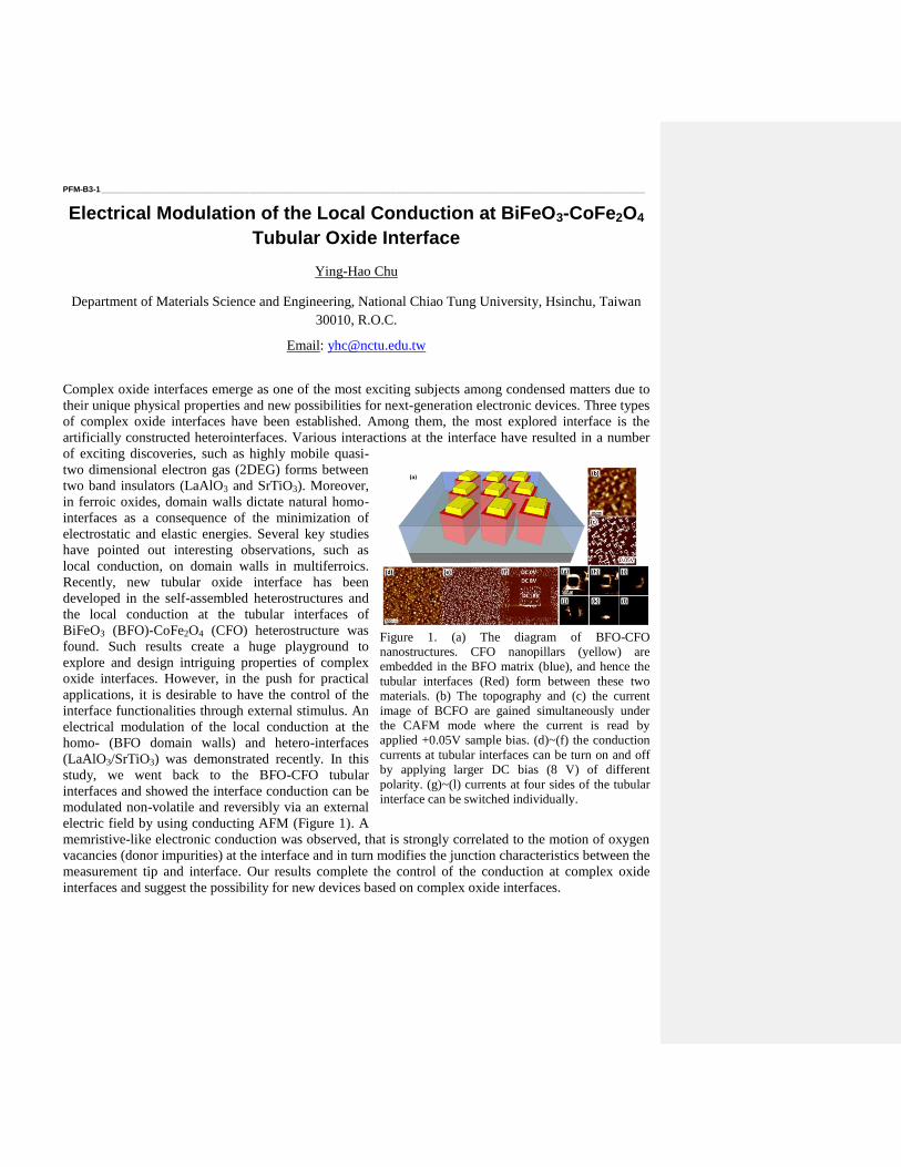
Figure 1. (a) The diagram of BFO-CFO
nanostructures. CFO nanopillars (yellow) are
embedded in the BFO matrix (blue), and hence the
tubular interfaces (Red) form between these two
materials. (b) The topography and (c) the current
image of BCFO are gained simultaneously under
the CAFM mode where the current is read by
applied +0.05V sample bias. (d)~(f) the conduction
currents at tubular interfaces can be turn on and off
by applying larger DC bias (8 V) of different
polarity. (g)~(l) currents at four sides of the tubular
interface can be switched individually.
PFM-B3-2 ______________________________________________________________________________________________________________________
Anomalous Photovoltaic effect in BiFeO3 Akash Bhatnagar, Marin Alexe
Max Planck Institute of Microstructure Physics
Weinberg 1, 06120 Halle (Saale),Germany
e-mail: [email protected]
In the recent past, the entire field of photo-ferroelectrics has been revitalized by the reports of
photovoltaic (PV) effect in BFO. Unlike traditional semiconductors the open circuit voltages in BFO are
not limited by band gap. Initial investigations assumed that the PV effect in BFO is primarily due to the
presence of a potential step at the domain wall which enables a more efficient separation of charge
carriers [xvi
]. However, in a recent work [xvii
] it was observed that the generation and recombination of
photo-generated non-equilibrium carriers in a BFO single crystal are primarily affected by the presence
of shallow energy levels and the domain walls might not playing a major in the corresponding PV effect,
as initially proposed. Thus, till now there is not yet a clear model of the PV effect in BFO. In this work,
in order to get a further insight into the actual mechanism for the generation of PV effect in epitaxial
BFO thin films, time and temperature resolved measurements have been performed. Time resolved
measurements, namely photo induced transient spectroscopy (PITS) bring valuable data regarding
generation and recombination of the photo-excited carriers. Providing that the ferroelectric domain
configuration in BFO does not change at low temperature, variable temperature measurements of PV
effect can provide information on details regarding the electronic structure of BFO, respectively shallow
or deep levels in the band gap, that may affect the conduction mechanism as reported in [2].
PFM-B3-3 ______________________________________________________________________________________________________________________
Optimization of carbon nanotube tips for improved scanning
probe microscopy studies of ferroic thin films
Yuliya Lisunova1*
, J Heidler2, I. Levkivskyi
3, I. Gaponenko
1, A. Weber
2, L.J. Heyderman
2, C.Cailler
1,
M. Klaui4 and P. Paruch
1
1DPMC-MaNEP, University of Geneva, 24 Quai Ernest-Ansermet, 1211 Geneva 4,Switzerland
2Paul Scherrer Institut , 5232 Villigen PSI, Switzerland
3DPT, University of Geneva, 24 Quai Ernest-Ansermet, 1211 Geneva 4, Switzerland
4University of Mainz, Institute of Physics, Staudinger Weg 7, 55128 Mainz, Germany
Email: [email protected]
Scanning probe microscopy is an essential research tool for both fundamental and technology-driven
studies, mapping diverse functional properties in a wide range of materials with a nanoscale resolution,
defined by the specific tip geometry and properties. Its imaging capacity can be significantly enhanced
by carbon-nanotube-based (CNT) tips [1], whose small size and outstanding mechanical and electrical
properties improve resolution in topographical, electrostatic and surface potential microscopy modes.
Further modification of the CNT tips [2-3] extends their application to magnetic force microscopy, when
ferromagnetically coated, and to contact-based techniques, when rigidified with an insulating silicon
dioxide layer. In the rapidly developing field of domain wall nanoelectronics [4], such ultra-high
resolution tips could provide unprecedented access to the novel and highly localized functional
properties of domain walls in ferroelectric and magnetic materials.
Here, we report on extended studies of such CNT tips, benchmarking their properties against
commercially available tips on ferroic thin films. Introducing molecular beam epitaxy deposition of
cobalt on single-walled CNT, we demonstrate sub-10 nm resolution in hard magnetic samples, and non-
perturbative magnetic force microscopy imaging of complex domain and domain wall (DW) structures
in micropatterned permalloy, both at ambient conditions [5]. We also develop theoretical models
allowing us to extract the key imaging parameters and their dependence on the tip properties, and tailor
the tip design to optimize resolution under given measurement conditions [5]. Integrating rigidified tips
in ferroelectric thin film studies, we demonstrate more precise spatial resolution of the conducting
region, allowing us to determine the minimal separation of DW in potential nanoelectronic devices, and
the writing and reading of ferroelectric domain structures. These results are expected to have an impact
on future probe-based technology, data storage and material characterization.
References
[1] J.H. Hafner et al. J. Am. Chem. Soc. 121, 9750 (1999)
[2] H. Kuramochi et al. Nanotechnology. 16, 24 (2005)
[3] N. Tayebi et al. Appl. Phys. Lett. 93, 103112 (2008)
[4] G. Catalan et al. Rev. Mod. Phys. 84, 119 (2012)
[5] Y. Lisunova et al. Nanotechnology 24 105705 (2013)
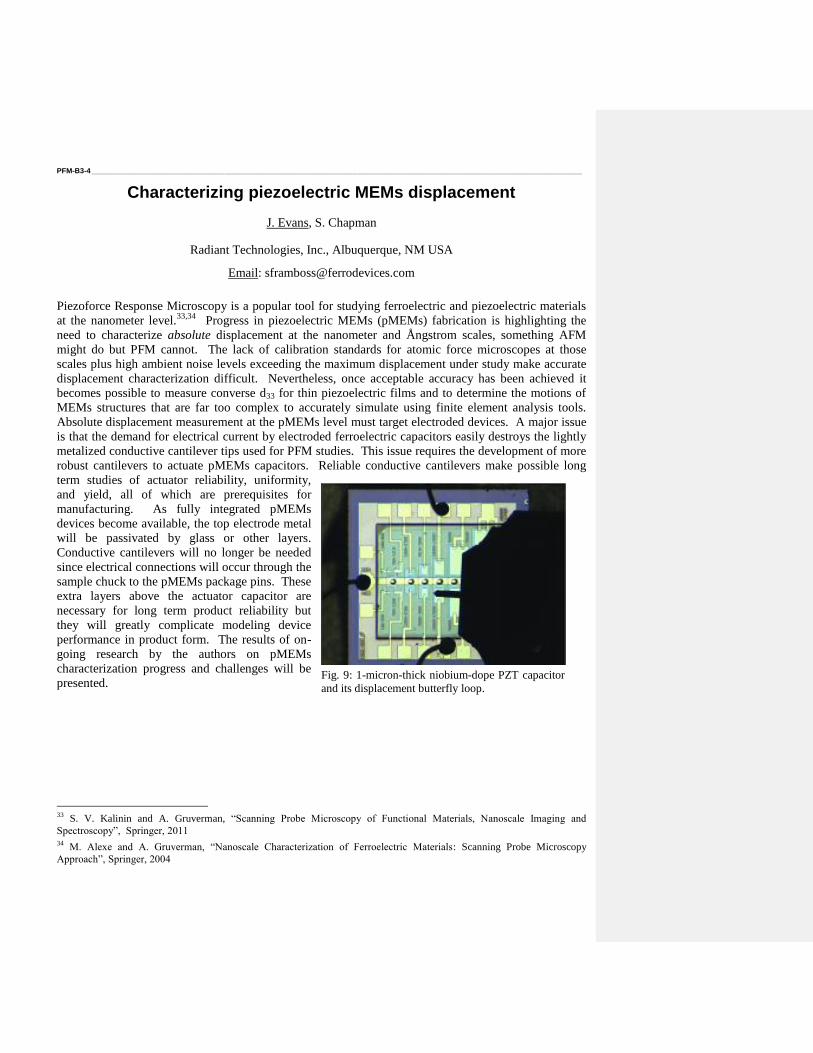
PFM-B3-4 ______________________________________________________________________________________________________________________
Characterizing piezoelectric MEMs displacement
J. Evans, S. Chapman
Radiant Technologies, Inc., Albuquerque, NM USA
Email: [email protected]
Piezoforce Response Microscopy is a popular tool for studying ferroelectric and piezoelectric materials
at the nanometer level.33,34
Progress in piezoelectric MEMs (pMEMs) fabrication is highlighting the
need to characterize absolute displacement at the nanometer and Ångstrom scales, something AFM
might do but PFM cannot. The lack of calibration standards for atomic force microscopes at those
scales plus high ambient noise levels exceeding the maximum displacement under study make accurate
displacement characterization difficult. Nevertheless, once acceptable accuracy has been achieved it
becomes possible to measure converse d33 for thin piezoelectric films and to determine the motions of
MEMs structures that are far too complex to accurately simulate using finite element analysis tools.
Absolute displacement measurement at the pMEMs level must target electroded devices. A major issue
is that the demand for electrical current by electroded ferroelectric capacitors easily destroys the lightly
metalized conductive cantilever tips used for PFM studies. This issue requires the development of more
robust cantilevers to actuate pMEMs capacitors. Reliable conductive cantilevers make possible long
term studies of actuator reliability, uniformity,
and yield, all of which are prerequisites for
manufacturing. As fully integrated pMEMs
devices become available, the top electrode metal
will be passivated by glass or other layers.
Conductive cantilevers will no longer be needed
since electrical connections will occur through the
sample chuck to the pMEMs package pins. These
extra layers above the actuator capacitor are
necessary for long term product reliability but
they will greatly complicate modeling device
performance in product form. The results of on-
going research by the authors on pMEMs
characterization progress and challenges will be
presented.
33
S. V. Kalinin and A. Gruverman, “Scanning Probe Microscopy of Functional Materials, Nanoscale Imaging and
Spectroscopy”, Springer, 2011 34
M. Alexe and A. Gruverman, “Nanoscale Characterization of Ferroelectric Materials: Scanning Probe Microscopy
Approach”, Springer, 2004
Fig. 9: 1-micron-thick niobium-dope PZT capacitor
and its displacement butterfly loop.

Lead-free ceramics: Structure
CLUB A
Monday, July 22 2013, 04:30 pm - 06:00 pm
Chair: Jacob Jones
University of Florida
ISAF3-C1-1 ____________________________________________________________________________________________________________________
Tilted or Distorted Octahedra in Perovskite Structures - what is the limit of what we can learn from powder diffraction?
Pam Thomas1, Mike Glazer
1&2, Dean Keeble
1, David Woodward
1
1 Department of Physics, University of Warwick, Coventry CV4 7AL, UK
2 Clarendon Laboratory, Parks Road, Oxford OX1 3PU, UK
Email: [email protected]
Powder diffraction, whether by x-rays or neutrons, is well known as a technique for “finger-printing”
crystal structures of all sorts, with automated search-match procedures and databases such as the ICDD
making this practice relatively routine in many cases. However, when dealing with highly pseudo-
symmetric structures that are derived either actually or theoretically from a cubic aristotype, powder
diffraction patterns must be scrutinized with considerable rigour and one must rationally discriminate
between very similar refinement fits to derive the correct structural model. In so doing, factors such as
the resolution of the experiment and the broadening contributed by the sample must also be correctly
accounted for.
In perovskite structures it has well been known since the seminal work of Glazer in the 1970’s, that the
structure can distort via tilting (rotating) of the oxygen octahedra about the unit cell axes of the parent
phase. These tilts can be classified according to the Glazer notation and their effects on the powder
pattern calculated. In particular, different systems of oxygen octahedral tilts lead to doublings of the unit
cell, which are detected via super-structure peaks (often called “tilt peaks” in common parlance). It is
usual for materials scientists (physicists, chemists etc) to look for particular super-structure peaks e.g.
or in a powder pattern to conclude that they have antiphase or in-phase octahedral
tilts, respectively.
In recent work on refinements of the crystal structure of the archetypal lead-free piezoelectric sodium
bismuth titanate, Na0.5Bi0.5TiO3 (NBT), in its tetragonal phase (at T>673K), we have discovered a
previously unconsidered characteristic of powder patterns for perovskites. In this talk, we will show how
there is a degeneracy in the powder patterns for (a) a tilted octahedral model of the structure or (b) a
distorted but untilted octahedral model of the structure. The effect of this is that the computed powder
patterns of these two quite different structures are virtually indistinguishable from each other, a very
unusual situation in powder diffraction! The implications of this for the wider interpretation of powder
diffraction data for a range of perovskite structures, including some fluorides with highly distorted
(fluorine) octahedra, are discussed.
ISAF3-C1-3 ____________________________________________________________________________________________________________________
Lead-free Piezoelectric Ceramics (Na0.5K0.5)NbO3 doped with LiTaO3 and BiScO3
Fangyuan ZHU1, Jing-Feng Li
1, Michael B. Ward
2, Tim P. Comyn
2, Andrew J. Bell
2 and Steven J.
Milne2
1School of Materials Science and Engineering, Tsinghua University, Beijing, China
2Institute for Materials Research, SPEME, University of Leeds, Leeds, UK
Email: [email protected]
A series of compositions along the compositional join in the ternary NKN-LT-BS system,
extending from 0.98Na0.5K0.5NbO3-0.02BiScO3 toward LiTaO3 have been prepared and characterized. A
composition [NKN0.98-(LiTaO3)0.02]0.98–[BiScO3]0.02 showed enhanced piezoelectric properties, relative
to similar compositions, with d33 values of 215 pC/N. This can be attributed to a phase content of mixed
orthorhombic (or monoclinic) and tetragonal phases at ambient temperatures. Variable temperature X-
ray diffraction (XRD), and dielectric measurements as a function of temperature, indicated phase
transitions (on heating) from an orthorhombic (or monoclinic) crystal system to tetragonal and then
cubic crystal systems at ~25°C and ~370°C respectively.
Different types of dielectric behavior were observed on increasing the LT content. A NKN-
5%LT-2%BS composition exhibited twin dielectric peaks at high temperatures (~370°C and ~470°C),
along with broad X-ray diffraction peaks and a fine grain size, < 0.5 μm. The twin dielectric peaks
suggest that chemical inhomogeneities may have been present; this was examined using transmission
electron microscopy (TEM) with energy dispersive X-ray analysis (EDX). Elemental segregation was
observed within individual grains, such that a core-shell grain structure was evident. Subsequently, a
series of other compositions were prepared in the wider Na0.5K0.5NbO3-LiTaO3-BiScO3 ternary system.
Considering the combined data from XRD, dielectric measurements, SEM, TEM and
piezoelectric properties for a wide range of compositions within the NKN-rich region of the NKN-LT-
BS system, materials may be grouped into three categories, exhibiting the following defining
characteristics.
Type I: single, sharp dielectric Curie peak (~370°C); single phase by XRD; large grain size (5-
10μm); chemically uniform by TEM-EDX.
Type II: broad, single dielectric peak (~350°C); single phase by XRD; large grain size; no
obvious chemical segregation.
Type III: twin, broad dielectric peak(s) (~370°C and ~470°C); broad XRD peaks; small grain
size (~0.5μm); chemical segregation (core-shell structure) identified by TEM-EDX.
ISAF3-C1-4 ____________________________________________________________________________________________________________________
Breaking of the centric symmetry in ferroelectric and paraelectric
phases of unpoled ceramics.
Alberto Biancoli1 and Dragan Damjanovic
1
1Ceramics Laboratory, Swiss Federal Institute of Technology in Lausanne –EPFL, Switzerland.
Email: [email protected]
In the recent years, flexoelectricity attracted a growing interest as an electro-mechanical coupling
mechanism alternative to piezoelectricity and electrostriction. Flexoelectric polarization is proportional
to elastic strain gradient, which scales inversely with the size of sample, and thus was in general
expected to play a major role only on nano-scale. In the past decade however, the experimental finding
of large apparent flexoelectric coefficients in bulk ferroelectrics (three to four order of magnitude larger
than theoretically predicted) raised the hope to exploit flexoelectricity for practical applications in bulk
materials as well.
On the other hand, the recent observation of piezoelectric and pyroelectric-like responses in unpoled
ferroelectric and paraelectric phases of ceramics suggests a breaking of the macroscopic centric
symmetry caused by a mechanism other than the already known symmetry breaking induced under
electric field. An insight into the origin of this breaking of the symmetry would have important
implications on the understanding of the flexoelectric effect in bulk materials and may provide an
explanation for the unexpectedly high apparent flexoelectric polarization reported for some bulk
materials.
We report here on investigations of the described spontaneous symmetry breaking in unpoled ceramics.
Materials examined include BaTiO3, SrTiO3, Ba1-xSrxTiO3, (Ba,Ca)(Zr,Ti)O3 and PbZr1-xTixO3 solid
solutions. Barium titanate, Ba1-xSrxTiO3, (Ba,Ca)(Zr,Ti)O3 were examined both below and above their
Curie temperature. A number of systematic studies were performed in a search for a possible driving
force for the symmetry breaking.
The influence of dielectric permittivity, temperature, surface electrodes and grain size on apparent
electro-mechanical and pyroelectric response of unpoled ferroelectric and paraelectric samples were
studied. Grain size of a BaTiO3 sample could be changed by thermal annealing. A fine-grained BaTiO3
sample with a large permittivity exhibits a lower pyroelectric response than the same sample with a
larger grain size and a lower permittivity. Response in BaTiO3 and SrTiO3 ceramics was compared to
that in respective single crystals. Both ceramics and single crystals of BaTiO3 exhibit nonzero
piezoelectric and pyroelectric signals above the Curie temperature. Within resolution of our
measurements, neither single crystal nor ceramics of SrTiO3 show any symmetry breaking at room
temperature. Pressing and sintering conditions for ceramics were analyzed and it was found that the
cooling rate after sintering does not significantly affect the response.
ISAF3-C1-5 ____________________________________________________________________________________________________________________
Laser Beam Scanning Microscopy Observation of Domain
Switching in NaNbO3 Epitaxial Film
Ichiro Fujii, Akihiro Kohori, Seiji Yamazoe, and Takahiro Wada
Department of Materials Chemistry, Ryukoku University, Otsu, Shiga, Japan
Email: [email protected]
Domain switching, or polarization reversal, substantially affects the dielectric and piezoelectric
properties of ferroelectric materials. Thus, it is important to understand how the domain structure
changes with the electric field amplitude. Laser beam scanning microscopy (LSM) with a polarizer is a
methodology that allows us to see domain patterns and their polarization directions.35, 2
We applied this
technique to a 001-oriented NaNbO3 (NN) film, and observed a drastic change in the domain structure
after a large electric field of 230 kV/cm was applied. In this study, evolution of the domain patterns of
ferroelectric 001-oriented NN film was observed using LSM during application of ac electric fields with
smaller amplitudes, and the domain structures were analyzed.
Before deposition of the NN film, we deposited SrRuO3 (SRO) film as a bottom electrode on (001)
SrTiO3(STO) substrate by pulsed laser deposition (PLD). Then, a 001-oriented NN film was prepared on
a (001) SRO/(001)STO substrate by PLD. Pt top electrodes were formed on the NN film by sputtering.
An electric field large enough to induce the ferroelectric response was applied by measuring polarization
– electric field (P-E) loops with a ferroelectric tester. The domain structures were observed by LSM
during the application of a triangular electric field. Here, a polarizer was placed between the film and the
objective lens, and rotated to see the polarization directions of the domains.
A ferroelectric P-E loop was observed for the NN film when an ac electric field amplitude of 100 kV/cm
was applied. Figure 1 (a) shows a
representative LSM image of the NN film.
Rotation of the polarizer found that the
domain structure consisted of the vertical and
horizontal domains and the slanted domains, as
illustrated in Fig. 1 (b). When the electric field
decreased from maximum electric field
(+Emax) to minimum electric field (–Emax), two
different domain-switching routes were
observed. One is that the slanted domains
changed to vertical and horizontal domains,
which then reverted to slanted domains. These
changes indicated that the polarization
direction, for example, changed from out-of- plane
[101] to in-plane [110] and to out-of-plane [10-1].
The other route will be also discussed.
35
S. Yamazoe, H. Sakurai, T. Saito, and T. Wada, Appl. Phys. Lett., 96, 092901 (2010). 2 S. Yamazoe et al., J. Appl. Phys. 112, 052007 (2012).
Fig. 1: (a) LSM image of NN film using 45˚
polarized laser beam, and (b) schematics of
polarization directions of domains.

Materials for High Power and High Temperature Applications
CLUB B
Monday, July 22 2013, 04:30 pm - 06:00 pm
Chair: Ian Reaney
University of Sheffield
ISAF1-C2-1 ____________________________________________________________________________________________________________________
BaTiO3 – Bi(Zn1/2Ti1/2)O3 – NaNbO3 Dielectric Ceramics for
Advanced Capacitor Applications
Natthaphon Raengthon1, Harlan J. Brown-Shaklee
2, Geoff L. Brennecka
2 and David P. Cann
1
1Materials Science, School of Mechanical, Industrial, and Manufacturing Engineering,
Oregon State University, Corvallis, OR, USA 2Electronic, Optical, and Nanostructured Materials Department, Sandia National Laboratories,
Albuquerque, NM, USA
Email: [email protected]
Dielectric ceramics for high temperature electronics are desired for advanced technologies since existing
technologies of ceramic capacitors (X7R or NP0) are not compatible with extreme environments, especially
at temperatures higher than 200 ºC. In recent years, several research groups have developed new BaTiO3 –
based materials that exhibit promising dielectric properties for high temperature applications. Previous
studies on BaTiO3 – Bi(Zn1/2Ti1/2)O3 – BiScO3 ceramics demonstrated that a temperature-stable permittivity
can be obtained over a broad temperature range36. However, a large change in permittivity between room
temperature and 100 ºC persisted which might limit the usage of the material over that temperature range.
Therefore, BaTiO3 – Bi(Zn1/2Ti1/2)O3 – NaNbO3 ceramic solid solutions were investigated. The effects of
BaTiO3 and NaNbO3 additions on the dielectric properties of ternary compounds are of interest. A
broadening of the temperature-dependent permittivity maximum and a decrease in overall permittivity were
observed when the content of BaTiO3 decreased while the Bi(Zn1/2Ti1/2)O3:NaNbO3 ratios were kept
constant. A shift in the temperature of the maximum permittivity (Tmax) down to -103 ºC was achieved when
substituting Bi(Zn1/2Ti1/2)O3 with NaNbO3 for the compositions with constant BaTiO3 concentration. A
broad permittivity peak was observed in several compositions that was comparable to other BaTiO3 –
Bi(Zn1/2Ti1/2)O3 based ceramics as shown in Figure 1. The
dielectric characteristics of the 50BT-25BZT-25NN
composition also satisfies the X9R standard (ΔC/C25 = ±15%
over a range of -55 to 200 ºC). A linear dielectric response is
also presented under high electric fields at various
temperatures. In conclusion, the investigation of BT-BZT-
NN compounds resulted in promising dielectric properties
with broad temperature ranges with a high permittivity, which
is of interest for advanced capacitor applications.
36N. Raengthon, T. Sebastian, D. Cumming, I. M. Reaney, and D. P. Cann, “BaTiO3 – Bi(Zn1/2Ti1/2)O3 – BiScO3 Ceramics for High-
Temperature Capacitor Applications”, J. Am. Ceram. Soc., 95[11] 3554-3561 (2012).
Sandia National Laboratories is a multi-program laboratory managed and operated by Sandia Corporation, a wholly owned subsidiary of
Lockheed Martin Corporation, for the U.S. Department of Energy’s National Nuclear Security Administration under contract DE-AC04-
94AL85000. This work was supported by the Department of Energy’s Office of Electricity Delivery and Energy Reliability, Energy
Storage Systems program managed by Dr. Imre Gyuk.
Figure 1. Temperature dependence of relative permittivity of Bi(Zn1/2Ti1/2)O3 – BaTiO3 based
compounds (BZT: Bi(Zn1/2Ti1/2)O3, BT: BaTiO3, BI: BiInO3, BS: BiScO3, NN: NaNbO3).
ISAF1-C2-2 ____________________________________________________________________________________________________________________
Large Field Property Assessment of Mn:PIN-PMN-PT Crystals for
High Power Transducers
Jun Luo1, Sam Taylor
1, Shujun Zhang
2 and W. Hackenberger
1
1TRS Technologies, Inc, State College, PA 16801
2Material Research Institute, Pennsylvania State University, PA16801
Email: [email protected]
The third generation of advanced relaxor-PT piezoelectric single crystals, Mn:PIN-PMN-PT (manganese
doped Pb(In1/2Nb1/2)O3-Pb(Mg1/3Nb2/3)O3-PbTiO3), has attracted broad attention for the high power
transducers due to their greatly reduced mechanical loss but well-maintained, extremely high
electromechanical coupling coefficient. Small signal characterization of Mn:PIN-PMN-PT crystals have
been extensively studied. However, systematic large signal tests of Mn:PIN-PMN-PT crystals were
urgently needed for further assessing the properties for high power transducer operation.
A systematic large signal, quasistatic measurement has been conducted for Mn:PIN-PMN-PT crystals
under variable prestress, temperature and electric field. Preliminarily optimized operation domains for
high power transducer design have been revealed for [001]-poled crystals for achieving maximum
acoustic power density with low hysteretic losses caused by nonlinearity and phase transitions. It was
proved that the uniaxial prestress can stabilize the rhombohedral phase and suppress the electric field
induced phase transition. Furthermore, driven by a combination of a bipolar AC field and a positive DC
bias field, the crystals exhibit a broader range of linear strain and polarization response under uniaxial
prestress, which means, at room temperature, a positive DC bias field (applied in the same direction with
the poling field) expands the linear range of strain response under a bipolar AC field (1Hz). As shown in
Fig. 1, for a +4kV/cm DC bias, the crystal was driven by a 6kV/cm bipolar AC field with no domain
switch. A larger AC field driving range may benefit the high power transducer applications.
Fig. 1: S-E loops of a Mn: PIN-PMN-PT crystal sample measured under 10MPa prestress and
4kV/cm external DC bias: (a) for 1-15kV/cm bipolar fields and (b) for 1-6kV/cm bipolar fields
ISAF1-C2-3 ____________________________________________________________________________________________________________________
Effects of excess Bi on high-temperature dielectric and
piezoelectric properties of lead-free 0.75BiFeO3-0.25BaTiO3
ceramics
Jianguo Chen , Jinrong Cheng1
1 School of Materials Science and Engineering, Shanghai University, Shanghai, People’s Republic of
China
Email: [email protected]
0.75BiFeO3-0.25BaTiO3 (BF-BT) ceramics with different excess Bi contents were prepared by solid
state reaction method. The effects of excess Bi content on the structure, dielectric and piezoelectric
properties of BF-BT ceramics were studied. XRD results indicated that the modified BF-BT ceramics
exhibited single perovskite structure with rhombohedral symmetry. The introduction of excess Bi in the
solid solutions showed positive effects on both dielectric and piezoelectric properties. The Curie
temperature Tc, dielectric constant and loss tan (1 kHz), piezoelectric constant d33, and planner
electromechanical coupling factor kp of BF-BT ceramics with 1 % excess Bi were 514 oC, 230, 440, 4.6
%, 115 pC/N and 0.28, respectively. The piezoelectric constant d33, and planner electromechanical
coupling factor kp of BF-BT ceramics with 1 % excess Bi were stable up to 450 oC, about 300
oC higher
than that of PZT-based ceramics. The combination of improved piezoelectric constant d33 and
temperature stability indicated that BF-BT ceramics with excess Bi were promising candidates for high-
temperature and lead-free piezoelectric applications.
ISAF1-C2-4 ____________________________________________________________________________________________________________________
Novel high temperature BiFeO3-(K0.5Bi0.5)TiO3-PbTiO3
piezoceramics
Jim Bennett1, Andrew.J.Bell
1, Tim.J.Stevenson
1 and Tim.P.Comyn
1
1Institute for Materials Research, University of Leeds, Leeds, UK
Email: [email protected]
There is currently a need for high strain piezoelectric actuators that are capable of operating under
extreme temperatures and pressures in applications such as aerospace, deep sea oil drilling and in
chemical processing. PZT is currently the dominant piezoelectric ceramic material in actuators,
sensors and transducers, however, PZT has a restricted operating temperature.
Ceramics belonging to the (1-x-y)BiFeO3-x(K0.5Bi0.5)TiO3-yPbTiO3 system have been fabricated. X
-ray diffraction was utilized along with PUND, strain-field, polarization-field and high temperature
electrical measurements in order to characterize the new materials. The Curie temperatures, TC, of the
compositions presented far exceed those of PZT, coupled with piezoelectric coefficients in the region
of 152-225 pC/N. A link was found to exist between the c/a ratio of the tetragonal phase across the
MPB and TC.
This work also examines the extrinsic piezoelectric effect as a function of temperature using the
piezoelectric Rayleigh relations. The effects of composition upon intrinsic contributions, d33 and EC are
also detailed. The d33, intrinsic and extrinsic contributions of these materials were found to increase up
to 150 °C while adhering to the Rayleigh model. The composition with the highest room temperature d33
was found to have a Rayleigh coefficient of 58.83 x 10⁻¹⁸
(m2/V
2), an order of magnitude increase
compared to La-doped BiFeO3-PbTiO3. Ternary and psuedoquaternary systems have recently been subject to large amounts of research
as many of the possible binary systems have been explored. This has led to a raft of materials with
reported high piezoelectric coefficients; these are often electrostrictive or have limited operating
temperatures. This system shows that with only small amounts of a third end member such as potassium
bismuth titanate in BFPT, the electrical properties of a binary system can be drastically altered.

ISAF1-C2-5 ____________________________________________________________________________________________________________________
Clive Randall1, Dennis P. Shay
1, Russell Maier
1, Doo Hyun Choi
2, Michael Lanagan
3
1Materials Science and Engineering, The Pennsylvania State University, University Park, PA, USA,
2Materials Science and
Engineerign, The Pennsylvania State University, University Park, PA, USA, 3Engineering Science and Mechanics, The
Pennsylvania State University, University Park, PA, USA
Designing Dielectric Materials for High Power and Energy Density-a New Era for Capacitor Based
Applications
This paper will develop a rationale for new dielectric materials that are required for new high
temperature and high energy density capacitors. We will consider the voltage saturation issues in
nonlinear dielectrics, degradation, and breakdown processes. We will also consider the impact of
coupled dipole mechanisms on energy density and power density behavior of selected dielectric
materials . These new insights into high energy density capacitors could be applied to electrochemical
and hybrid capacitor designs.

PFM3
CLUB C
Monday, July 22 2013, 04:30 pm - 06:00 pm
Chair: Patrycja Paruch
University of Geneva
PFM-C3-1 ______________________________________________________________________________________________________________________
Interplay of polarization dynamic and surface electrochemistry in ferroelectrics: from ionic transport to
chaotic dynamics and fractal growth
S.V. Kalinin,1 A. Morozovska,
2 and V. Shur
3
1 The Center for Nanophase Materials Sciences, Oak Ridge National Laboratory,
Oak Ridge, TN 37922
2 Ferroelectric Laboratory, Institute of Natural Sciences, Ural Federal University,
620000 Ekaterinburg, Russia
3 Institute of Physics, National Academy of Sciences of Ukraine, 46, pr. Nauki, 03028 Kiev, Ukraine
Polarization switching in ferroelectric materials is inseparable from the screening processes, which in many cases
are realized by mobile surface ions. In this presentation, I will discuss experimental evidence for the existence and
slow dynamics of these ions based on variable temperature Kelvin Probe Microscopy data, and present
experimental strategies for exploring the injection and ionic transport phenomena based on the time-resolved
KPFM. The nontrivial effects of the ionic dynamics on domain structure and dynamics in ferroelectric thin films
and crystals, including metastable nanoscale phase separated domain states, slow switching dynamics, and
formation of fractal domains and chaotic dynamics during switching are discussed.
This work is supported by the Center for Nanophase Materials Sciences which is sponsored by the Scientific User
Facilities Division, Office of Basic Energy Sciences, U.S. Department of Energy
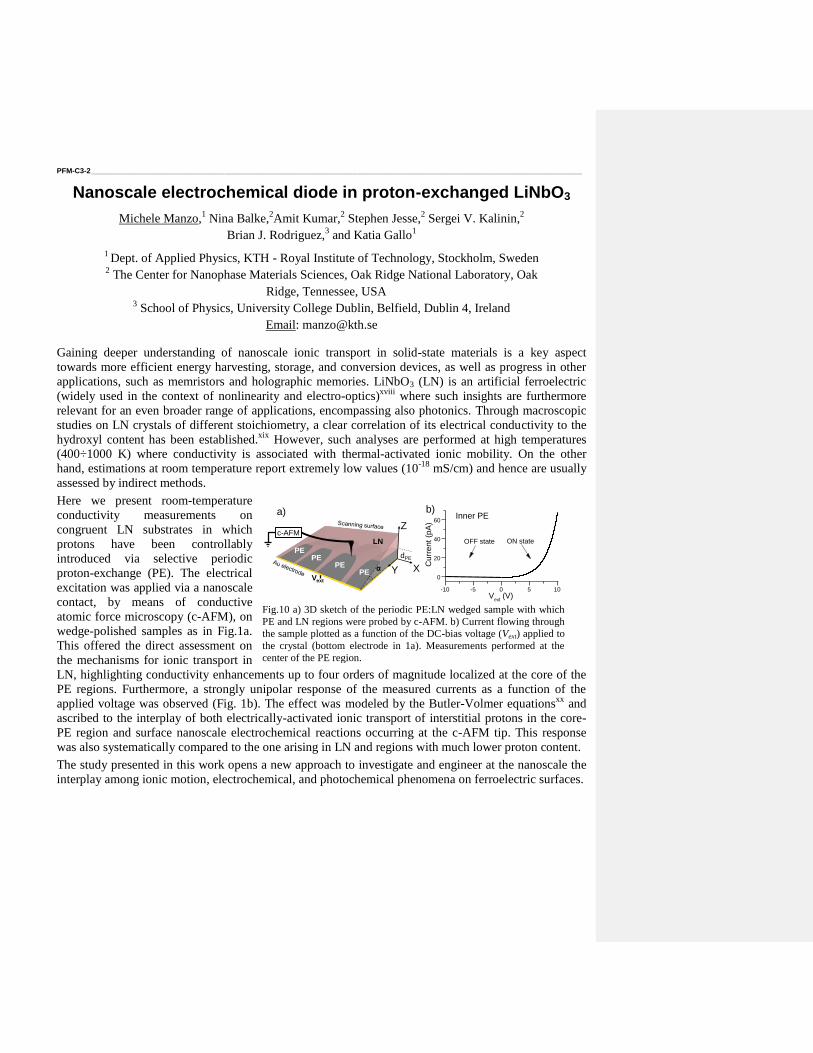
PFM-C3-2 ______________________________________________________________________________________________________________________
Nanoscale electrochemical diode in proton-exchanged LiNbO3
Michele Manzo,1 Nina Balke,
2Amit Kumar,
2 Stephen Jesse,
2 Sergei V. Kalinin,
2
Brian J. Rodriguez,3 and Katia Gallo
1
1 Dept. of Applied Physics, KTH - Royal Institute of Technology, Stockholm, Sweden
2 The Center for Nanophase Materials Sciences, Oak Ridge National Laboratory, Oak
Ridge, Tennessee, USA 3 School of Physics, University College Dublin, Belfield, Dublin 4, Ireland
Email: [email protected]
Gaining deeper understanding of nanoscale ionic transport in solid-state materials is a key aspect
towards more efficient energy harvesting, storage, and conversion devices, as well as progress in other
applications, such as memristors and holographic memories. LiNbO3 (LN) is an artificial ferroelectric
(widely used in the context of nonlinearity and electro-optics)xviii
where such insights are furthermore
relevant for an even broader range of applications, encompassing also photonics. Through macroscopic
studies on LN crystals of different stoichiometry, a clear correlation of its electrical conductivity to the
hydroxyl content has been established.xix
However, such analyses are performed at high temperatures
(400÷1000 K) where conductivity is associated with thermal-activated ionic mobility. On the other
hand, estimations at room temperature report extremely low values (10-18
mS/cm) and hence are usually
assessed by indirect methods.
Here we present room-temperature
conductivity measurements on
congruent LN substrates in which
protons have been controllably
introduced via selective periodic
proton-exchange (PE). The electrical
excitation was applied via a nanoscale
contact, by means of conductive
atomic force microscopy (c-AFM), on
wedge-polished samples as in Fig.1a.
This offered the direct assessment on
the mechanisms for ionic transport in
LN, highlighting conductivity enhancements up to four orders of magnitude localized at the core of the
PE regions. Furthermore, a strongly unipolar response of the measured currents as a function of the
applied voltage was observed (Fig. 1b). The effect was modeled by the Butler-Volmer equationsxx
and
ascribed to the interplay of both electrically-activated ionic transport of interstitial protons in the core-
PE region and surface nanoscale electrochemical reactions occurring at the c-AFM tip. This response
was also systematically compared to the one arising in LN and regions with much lower proton content.
The study presented in this work opens a new approach to investigate and engineer at the nanoscale the
interplay among ionic motion, electrochemical, and photochemical phenomena on ferroelectric surfaces.
b)
-10 -5 0 5 10
0
20
40
60Inner (
3) PE
Curr
ent
(pA
)
Vext
(V)
OFF state ON state
Inner PE
Vext
Z
Y X
LN
dPE
α
c-AFM
a)
PEPE
PE
PE
Fig.10 a) 3D sketch of the periodic PE:LN wedged sample with which
PE and LN regions were probed by c-AFM. b) Current flowing through
the sample plotted as a function of the DC-bias voltage (Vext) applied to
the crystal (bottom electrode in 1a). Measurements performed at the
center of the PE region.
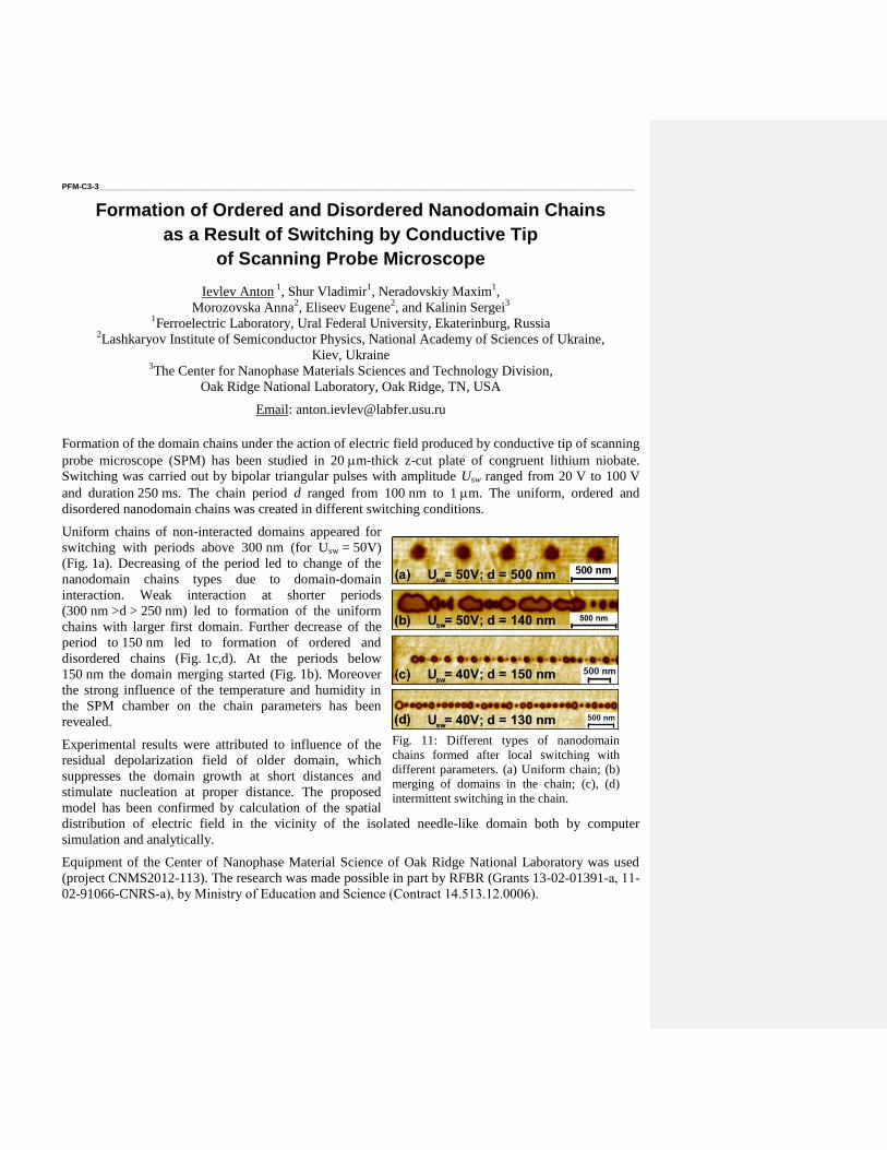
PFM-C3-3 ______________________________________________________________________________________________________________________
Formation of Ordered and Disordered Nanodomain Chains
as a Result of Switching by Conductive Tip
of Scanning Probe Microscope
Ievlev Anton 1, Shur Vladimir
1, Neradovskiy Maxim
1,
Morozovska Anna2, Eliseev Eugene
2, and Kalinin Sergei
3
1Ferroelectric Laboratory, Ural Federal University, Ekaterinburg, Russia
2Lashkaryov Institute of Semiconductor Physics, National Academy of Sciences of Ukraine,
Kiev, Ukraine 3The Center for Nanophase Materials Sciences and Technology Division,
Oak Ridge National Laboratory, Oak Ridge, TN, USA
Email: [email protected]
Formation of the domain chains under the action of electric field produced by conductive tip of scanning
probe microscope (SPM) has been studied in 20 m-thick z-cut plate of congruent lithium niobate.
Switching was carried out by bipolar triangular pulses with amplitude Usw ranged from 20 V to 100 V
and duration 250 ms. The chain period d ranged from 100 nm to 1 m. The uniform, ordered and
disordered nanodomain chains was created in different switching conditions.
Uniform chains of non-interacted domains appeared for
switching with periods above 300 nm (for Usw = 50V)
(Fig. 1a). Decreasing of the period led to change of the
nanodomain chains types due to domain-domain
interaction. Weak interaction at shorter periods
(300 nm >d > 250 nm) led to formation of the uniform
chains with larger first domain. Further decrease of the
period to 150 nm led to formation of ordered and
disordered chains (Fig. 1c,d). At the periods below
150 nm the domain merging started (Fig. 1b). Moreover
the strong influence of the temperature and humidity in
the SPM chamber on the chain parameters has been
revealed.
Experimental results were attributed to influence of the
residual depolarization field of older domain, which
suppresses the domain growth at short distances and
stimulate nucleation at proper distance. The proposed
model has been confirmed by calculation of the spatial
distribution of electric field in the vicinity of the isolated needle-like domain both by computer
simulation and analytically.
Equipment of the Center of Nanophase Material Science of Oak Ridge National Laboratory was used
(project CNMS2012-113). The research was made possible in part by RFBR (Grants 13-02-01391-а, 11-
02-91066-CNRS-а), by Ministry of Education and Science (Сontract 14.513.12.0006).
Fig. 11: Different types of nanodomain
chains formed after local switching with
different parameters. (a) Uniform chain; (b)
merging of domains in the chain; (c), (d)
intermittent switching in the chain.
PFM-C3-4 ______________________________________________________________________________________________________________________
Towards a Better Understanding of Lateral Piezoresponse Force
Microscopy
Shiming Lei1,2
, Ryan C. Haislmaier1, Tom T. A. Lummen
1, Wenwu Cao
2,3, Venkatraman Gopalan
1
1Materials Research Institute and Department of Materials Science and Engineering, Pennsylvania State
University, University Park, Pennsylvania, USA 2Condensed Matter Science and Technology Institute and Department of Physics, Harbin Institute of
Technology, Harbin, People's Republic of China 3Materials Research Institute and Department of Mathematics, Pennsylvania State University, University
Park, Pennsylvania 16802, USA
Email: [email protected]
Piezoresponse Force Microscopy (PFM) has been widely used for probing and imaging domain
structures of ferroelectric materials. In order to obtain a comprehensive information of probed polar
materials, both vertical and lateral signals are necessary to be used. In this sense, it is of vital importance
to bridge the PFM signal correctly to the corresponding properties of the probed materials.
Our previous theoretical calculations systematically analyzed the mechanisms of lateral and vertical
PFM response for Lithium Niobate single crystal (LiNbO3)37
. But for the realistic experimental signals,
they are always contaminated by the frequency-dependent background noise, which is inherent to the
experimental setup2. Jungk et al. proposed an effective treatment to recover vertical contrast. However,
to our best knowledge, no effective background noise treatment has been proposed for the lateral signal
so far, which undoubtedly holds back the quantitative understanding of lateral PFM signals. Here we
reported an effort towards eliminating the background noise in the lateral PFM signal. The results after
this treatment showed an excellent agreement with theoretical calculations. In addition, the 90° lateral
PFM signal scanning across the anti-parallel LiNbO3 domain wall, which was dismissed as an artefact
before, is confirmed with repeatable results in the present effort.
37
Lei et al, "Origin of piezoelectric response under a biased scanning probe microscopy tip across a 180° ferroelectric domain
wall", PHYSICAL REVIEW B 86, 134115 (2012) 2Jungk et al, "Quantitative analysis of ferroelectric domain imaging with piezoresponse force microscopy", Appl. Phys. Lett.
89 163507 (2006).
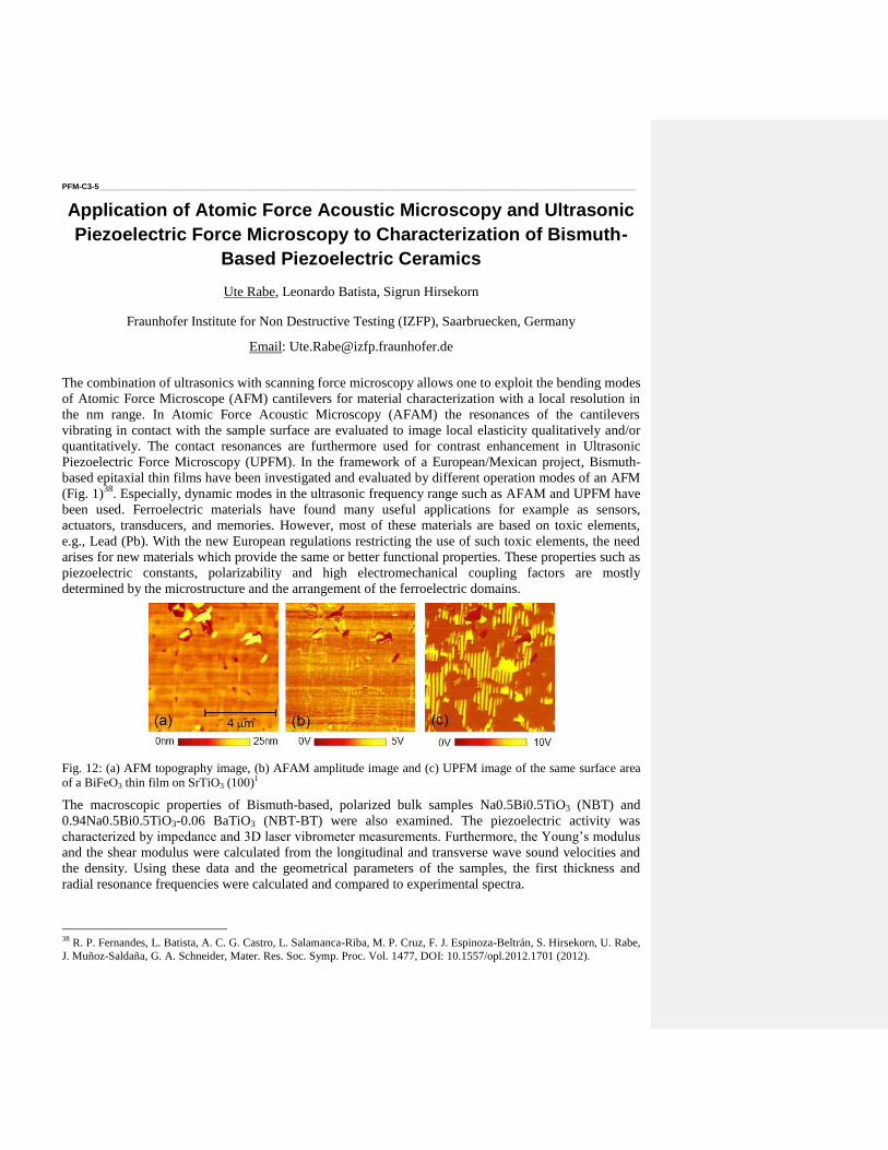
PFM-C3-5 ______________________________________________________________________________________________________________________
Application of Atomic Force Acoustic Microscopy and Ultrasonic
Piezoelectric Force Microscopy to Characterization of Bismuth-
Based Piezoelectric Ceramics
Ute Rabe, Leonardo Batista, Sigrun Hirsekorn
Fraunhofer Institute for Non Destructive Testing (IZFP), Saarbruecken, Germany
Email: [email protected]
The combination of ultrasonics with scanning force microscopy allows one to exploit the bending modes
of Atomic Force Microscope (AFM) cantilevers for material characterization with a local resolution in
the nm range. In Atomic Force Acoustic Microscopy (AFAM) the resonances of the cantilevers
vibrating in contact with the sample surface are evaluated to image local elasticity qualitatively and/or
quantitatively. The contact resonances are furthermore used for contrast enhancement in Ultrasonic
Piezoelectric Force Microscopy (UPFM). In the framework of a European/Mexican project, Bismuth-
based epitaxial thin films have been investigated and evaluated by different operation modes of an AFM
(Fig. 1)38
. Especially, dynamic modes in the ultrasonic frequency range such as AFAM and UPFM have
been used. Ferroelectric materials have found many useful applications for example as sensors,
actuators, transducers, and memories. However, most of these materials are based on toxic elements,
e.g., Lead (Pb). With the new European regulations restricting the use of such toxic elements, the need
arises for new materials which provide the same or better functional properties. These properties such as
piezoelectric constants, polarizability and high electromechanical coupling factors are mostly
determined by the microstructure and the arrangement of the ferroelectric domains.
Fig. 12: (a) AFM topography image, (b) AFAM amplitude image and (c) UPFM image of the same surface area
of a BiFeO3 thin film on SrTiO3 (100)1
The macroscopic properties of Bismuth-based, polarized bulk samples Na0.5Bi0.5TiO3 (NBT) and
0.94Na0.5Bi0.5TiO3-0.06 BaTiO3 (NBT-BT) were also examined. The piezoelectric activity was
characterized by impedance and 3D laser vibrometer measurements. Furthermore, the Young’s modulus
and the shear modulus were calculated from the longitudinal and transverse wave sound velocities and
the density. Using these data and the geometrical parameters of the samples, the first thickness and
radial resonance frequencies were calculated and compared to experimental spectra.
38
R. P. Fernandes, L. Batista, A. C. G. Castro, L. Salamanca-Riba, M. P. Cruz, F. J. Espinoza-Beltrán, S. Hirsekorn, U. Rabe,
J. Muñoz-Saldaña, G. A. Schneider, Mater. Res. Soc. Symp. Proc. Vol. 1477, DOI: 10.1557/opl.2012.1701 (2012).

ISAF Group 1 Posters
Forum Hall
Monday, July 22 2013, 01:00 pm - 04:30 pm
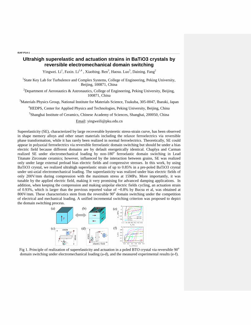
ISAF-P1A-1 ____________________________________________________________________________________________________________________
Ultrahigh superelastic and actuation strains in BaTiO3 crystals by reversible electromechanical domain switching
Yingwei. Li1, Faxin. Li
1,4 , Xiaobing. Ren
3, Haosu. Luo
5, Daining. Fang
2
1State Key Lab for Turbulence and Complex Systems, College of Engineering, Peking University,
Beijing, 100871, China
2Department of Aeronautics & Astronautics, College of Engineering, Peking University, Beijing,
100871, China
3Materials Physics Group, National Institute for Materials Science, Tsukuba, 305-0047, Ibaraki, Japan
4HEDPS, Center for Applied Physics and Technologies, Peking University, Beijing, China
5Shanghai Institute of Ceramics, Chinese Academy of Sciences, Shanghai, 200050, China
Email: [email protected]
Superelasticity (SE), characterized by large recoverable hysteretic stress-strain curve, has been observed
in shape memory alloys and other smart materials including the relaxor ferroelectrics via reversible
phase transformation, while it has rarely been realized in normal ferroelectrics. Theoretically, SE could
appear in polyaxial ferroelectrics via reversible ferroelastic domain switching but should be under a bias
electric field because different domains are by default energetically identical. Chaplya and Carman
realized SE under electromechanical loading by non-180o ferroelastic domain switching in Lead
Titanate Zirconate ceramics; however, influenced by the interaction between grains, SE was realized
only under large external preload bias electric fields and compressive stresses. In this work, by using
BaTiO3 crystal, we realized ultrahigh superelastic strain of up to 0.85% in a pre-poled BaTiO3 crystal
under uni-axial electromechanical loading. The superelasticity was realized under bias electric fields of
only 200V/mm during compression with the maximum stress at 15MPa. More importantly, it was
tunable by the applied electric field, making it very promising for advanced damping applications. In
addition, when keeping the compression and making unipolar electric fields cycling, an actuation strain
of 0.93%, which is larger than the previous reported value of ~0.8% by Bucsu et al, was obtained at
800V/mm. These characteristics stem from the reversible 90o domain switching under the competition
of electrical and mechanical loading. A unified incremental switching criterion was proposed to depict
the domain switching process.
Fig 1. Principle of realization of superelasticity and actuation in a poled BTO crystal via reversible 90
o
domain switching under electromechanical loading (a-d), and the measured experimental results (e-f).
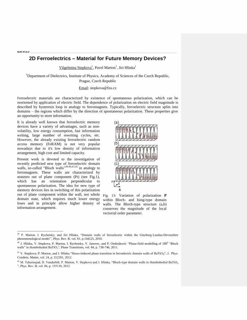
ISAF-P1A-2 ____________________________________________________________________________________________________________________
2D Ferroelectrics – Material for Future Memory Devices?
Vilgelmina Stepkova1, Pavel Marton
1, Jiri Hlinka
1
1Department of Dielectrics, Institute of Physics, Academy of Sciences of the Czech Republic,
Prague, Czech Republic
Email: [email protected]
Ferroelectric materials are characterized by existence of spontaneous polarization, which can be
reoriented by application of electric field. The dependence of polarization on electric field magnitude is
described by hysteresis loop in analogy to ferromagnets. Typically, ferroelectric structure splits into
domains – the regions which differ by the direction of spontaneous polarization. These properties give
an opportunity to store information.
It is already well known that ferroelectric memory
devices have a variety of advantages, such as non-
volatility, low energy consumption, fast information
writing, large number of rewriting cycles, etc.
However, the already existing ferroelectric random
access memory (FeRAM) is not very popular
nowadays due to it's low density of information
arrangement, high cost and limited capacity.
Present work is devoted to the investigation of
recently predicted new type of ferroelectric domain
walls, so-called “Bloch walls”39,40,41,42
in analogy to
ferromagnets. These walls are characterized by
nonzero out of plane component (Pt) (see Fig.1),
which has an orientation perpendicular to
spontaneous polarization. The idea for new type of
memory devices lies in switching of this polarization
out of plane component within the wall, not whole
domain state, which requires much lower energy
loses and in principle allow higher density of
information arrangement.
39
P. Marton, I. Rychetsky, and Jiri Hlinka, “Domain walls of ferroelectric within the Ginzburg-Landau-Devonshire
phenomenological model ”, Phys. Rev. B, vol. 81, p.144125, 2010. 40
J. Hlinka, V. Stepkova, P. Marton, I. Rychetsky, V. Janovec, and P. Ondrejkovic “Phase-field modelling of 1800 “Bloch
walls” in rhombohedral BaTiO3”, Phase Transitions, vol. 84, p. 738-746, 2011.
41 V. Stepkova, P. Marton, and J. Hlinka “Stress-induced phase transition in ferroelectric domain walls of BaTiO3”, J. Phys:
Condens. Matter, vol. 24, p. 212201, 2012. 42
M. Teherinejad, D. Vanderbilt, P. Marton, V. Stepkova and J. Hlinka, “Bloch-type domain walls in rhombohedral BaTiO3
”, Phys. Rev. B, vol. 86, p. 155138, 2012.
Fig. 13: Variation of polarization P
within Bloch- and Ising-type domain
walls. The Bloch-type structure (a,b)
conserves the magnitude of the local
vectorial order parameter.
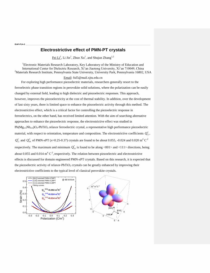
ISAF-P1A-3 ____________________________________________________________________________________________________________________
Electrostrictive effect of PMN-PT crystals
Fei Li1, Li Jin
1, Zhuo Xu
1, and Shujun Zhang
1,2
1Electronic Materials Research Laboratory, Key Laboratory of the Ministry of Education and
International Center for Dielectric Research, Xi’an Jiaotong University, Xi’an 710049, China 2Materials Research Institute, Pennsylvania State University, University Park, Pennsylvania 16802, USA
Email: [email protected]
For exploring high performance piezoelectric materials, researchers generally resort to the
ferroelectric phase transition regions in perovskite solid solutions, where the polarization can be easily
changed by external field, leading to high dielectric and piezoelectric responses. This approach,
however, improves the piezoelectricity at the cost of thermal stability. In addition, over the development
of last sixty years, there is limited space to enhance the piezoelectric activity through this method. The
electrostrictive effect, which is a critical factor for controlling the piezoelectric response in
ferroelectrics, on the other hand, has received limited attention. With the aim of searching alternative
approaches to enhance the piezoelectric response, the electrostrictive effect was studied in
Pb(Mg1/3Nb2/3)O3-PbTiO3 relaxor ferroelectric crystal, a representative high performance piezoelectric
material, with respect to orientation, temperature and composition. The electrostrictive coefficients C
11Q ,
C
12Q and C
44Q of PMN-xPT (x=0.25-0.37) crystals are found to be about 0.055, -0.024 and 0.020 m4 C
-2
respectively. The maximum and minimum *
33Q is found to be along <001> and <111> directions, being
about 0.055 and 0.014 m4 C
-2, respectively. The relation between piezoelectric and electrostrictive
effects is discussed for domain engineered PMN-xPT crystals. Based on this research, it is expected that
the piezoelectric activity of relaxor-PbTiO3 crystals can be greatly enhanced by improving their
electrostrictive coefficients to the typical level of classical perovskite crystals.
-0.3 -0.2 -0.1 0.0 0.1 0.2 0.3
0.0
0.1
0.2
0.3
0.4
0.5
Q11
[001]=0.053 m
4/C
2
Q11
[111]=0.014 m
4/C
2
Str
ain
(%
)
Polarization (C/m2)
[001] oriented PMN-0.28PT
[110] oriented PMN-0.28PT
[111] oriented PMN-0.28PT
Fitting curves
Q11
[110]=0.024 m
4/C
2
@ 80 kV/cm
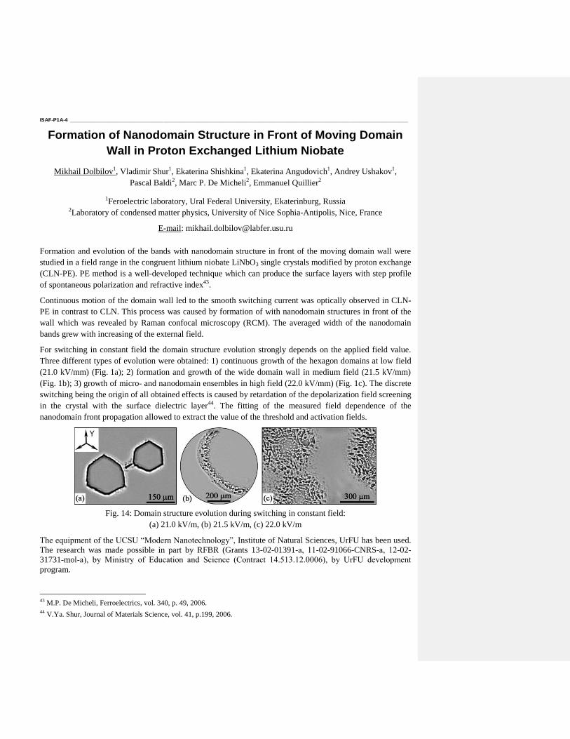
ISAF-P1A-4 ____________________________________________________________________________________________________________________
Formation of Nanodomain Structure in Front of Moving Domain
Wall in Proton Exchanged Lithium Niobate
Mikhail Dolbilov1, Vladimir Shur1, Ekaterina Shishkina1, Ekaterina Angudovich1, Andrey Ushakov1,
Pascal Baldi2, Marc P. De Micheli2, Emmanuel Quillier2
1Feroelectric laboratory, Ural Federal University, Ekaterinburg, Russia 2Laboratory of condensed matter physics, University of Nice Sophia-Antipolis, Nice, France
E-mail: [email protected]
Formation and evolution of the bands with nanodomain structure in front of the moving domain wall were
studied in a field range in the congruent lithium niobate LiNbO3 single crystals modified by proton exchange
(CLN-PE). PE method is a well-developed technique which can produce the surface layers with step profile
of spontaneous polarization and refractive index43.
Continuous motion of the domain wall led to the smooth switching current was optically observed in CLN-
PE in contrast to CLN. This process was caused by formation of with nanodomain structures in front of the
wall which was revealed by Raman confocal microscopy (RCM). The averaged width of the nanodomain
bands grew with increasing of the external field.
For switching in constant field the domain structure evolution strongly depends on the applied field value.
Three different types of evolution were obtained: 1) continuous growth of the hexagon domains at low field
(21.0 kV/mm) (Fig. 1a); 2) formation and growth of the wide domain wall in medium field (21.5 kV/mm)
(Fig. 1b); 3) growth of micro- and nanodomain ensembles in high field (22.0 kV/mm) (Fig. 1c). The discrete
switching being the origin of all obtained effects is caused by retardation of the depolarization field screening
in the crystal with the surface dielectric layer44. The fitting of the measured field dependence of the
nanodomain front propagation allowed to extract the value of the threshold and activation fields.
Fig. 14: Domain structure evolution during switching in constant field:
(a) 21.0 kV/m, (b) 21.5 kV/m, (c) 22.0 kV/m
The equipment of the UCSU “Modern Nanotechnology”, Institute of Natural Sciences, UrFU has been used.
The research was made possible in part by RFBR (Grants 13-02-01391-а, 11-02-91066-CNRS-а, 12-02-
31731-mol-а), by Ministry of Education and Science (Сontract 14.513.12.0006), by UrFU development
program.
43
M.P. De Micheli, Ferroelectrics, vol. 340, p. 49, 2006. 44
V.Ya. Shur, Journal of Materials Science, vol. 41, p.199, 2006.
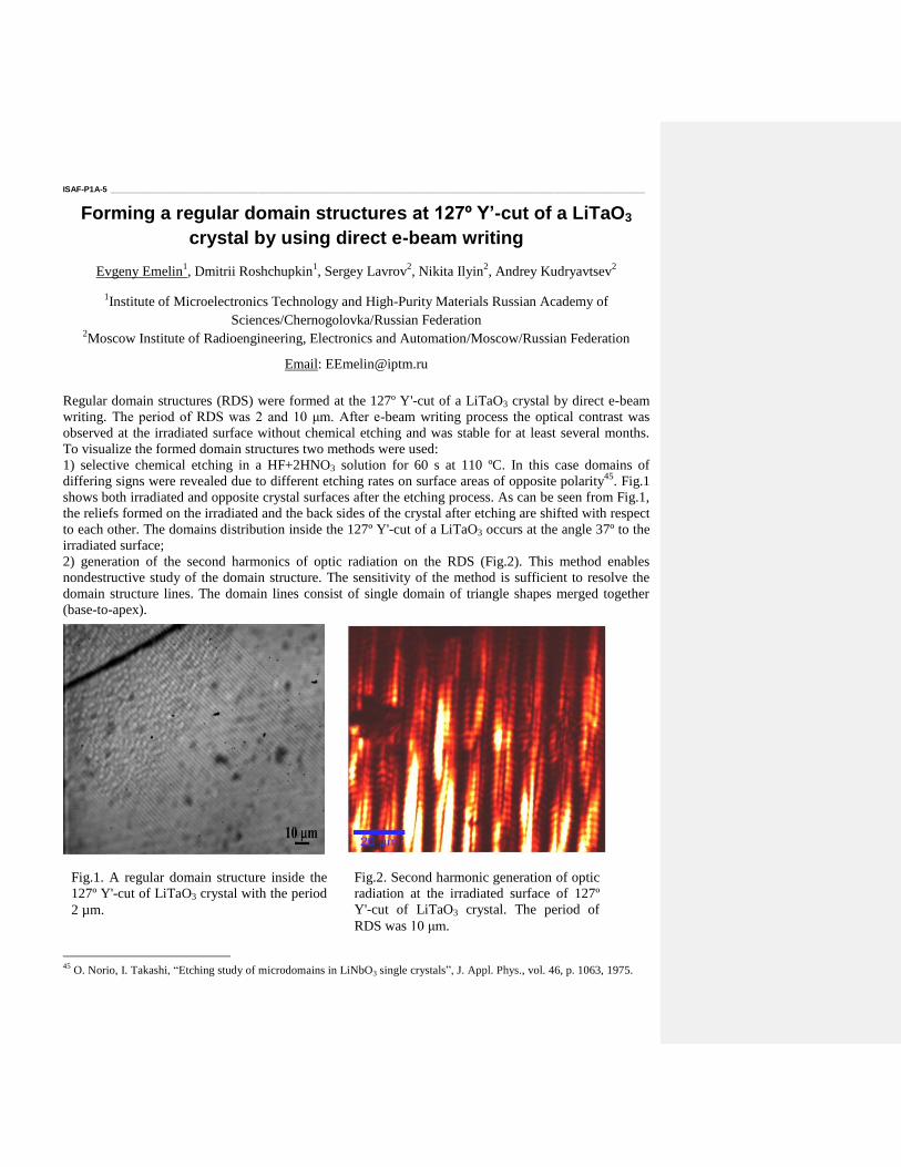
ISAF-P1A-5 ____________________________________________________________________________________________________________________
Forming a regular domain structures at 127º Y’-cut of a LiTaO3
crystal by using direct e-beam writing
Evgeny Emelin1, Dmitrii Roshchupkin
1, Sergey Lavrov
2, Nikita Ilyin
2, Andrey Kudryavtsev
2
1Institute of Microelectronics Technology and High-Purity Materials Russian Academy of
Sciences/Chernogolovka/Russian Federation 2Moscow Institute of Radioengineering, Electronics and Automation/Moscow/Russian Federation
Email: [email protected]
Regular domain structures (RDS) were formed at the 127º Y'-cut of a LiTaO3 crystal by direct e-beam
writing. The period of RDS was 2 and 10 μm. After e-beam writing process the optical contrast was
observed at the irradiated surface without chemical etching and was stable for at least several months.
To visualize the formed domain structures two methods were used:
1) selective chemical etching in a HF+2HNO3 solution for 60 s at 110 ºC. In this case domains of
differing signs were revealed due to different etching rates on surface areas of opposite polarity45
. Fig.1
shows both irradiated and opposite crystal surfaces after the etching process. As can be seen from Fig.1,
the reliefs formed on the irradiated and the back sides of the crystal after etching are shifted with respect
to each other. The domains distribution inside the 127º Y'-cut of a LiTaO3 occurs at the angle 37º to the
irradiated surface;
2) generation of the second harmonics of optic radiation on the RDS (Fig.2). This method enables
nondestructive study of the domain structure. The sensitivity of the method is sufficient to resolve the
domain structure lines. The domain lines consist of single domain of triangle shapes merged together
(base-to-apex).
45
O. Norio, I. Takashi, “Etching study of microdomains in LiNbO3 single crystals”, J. Appl. Phys., vol. 46, p. 1063, 1975.
Fig.1. A regular domain structure inside the
127º Y'-cut of LiTaO3 crystal with the period
2 µm.
Fig.2. Second harmonic generation of optic
radiation at the irradiated surface of 127º
Y'-cut of LiTaO3 crystal. The period of
RDS was 10 μm.
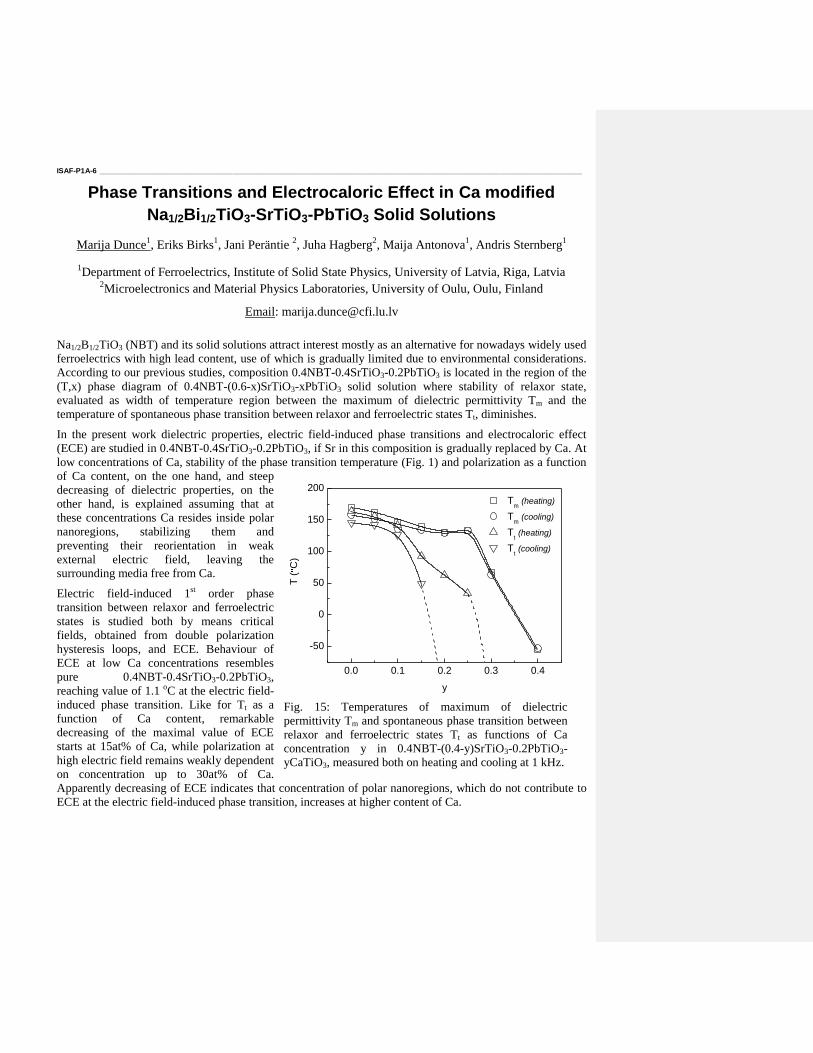
ISAF-P1A-6 ____________________________________________________________________________________________________________________
Phase Transitions and Electrocaloric Effect in Ca modified
Na1/2Bi1/2TiO3-SrTiO3-PbTiO3 Solid Solutions
Marija Dunce1, Eriks Birks
1, Jani Peräntie
2, Juha Hagberg
2, Maija Antonova
1, Andris Sternberg
1
1Department of Ferroelectrics, Institute of Solid State Physics, University of Latvia, Riga, Latvia
2Microelectronics and Material Physics Laboratories, University of Oulu, Oulu, Finland
Email: [email protected]
Na1/2B1/2TiO3 (NBT) and its solid solutions attract interest mostly as an alternative for nowadays widely used
ferroelectrics with high lead content, use of which is gradually limited due to environmental considerations.
According to our previous studies, composition 0.4NBT-0.4SrTiO3-0.2PbTiO3 is located in the region of the
(T,x) phase diagram of 0.4NBT-(0.6-x)SrTiO3-xPbTiO3 solid solution where stability of relaxor state,
evaluated as width of temperature region between the maximum of dielectric permittivity Tm and the
temperature of spontaneous phase transition between relaxor and ferroelectric states Tt, diminishes.
In the present work dielectric properties, electric field-induced phase transitions and electrocaloric effect
(ECE) are studied in 0.4NBT-0.4SrTiO3-0.2PbTiO3, if Sr in this composition is gradually replaced by Ca. At
low concentrations of Ca, stability of the phase transition temperature (Fig. 1) and polarization as a function
of Ca content, on the one hand, and steep
decreasing of dielectric properties, on the
other hand, is explained assuming that at
these concentrations Ca resides inside polar
nanoregions, stabilizing them and
preventing their reorientation in weak
external electric field, leaving the
surrounding media free from Ca.
Electric field-induced 1st order phase
transition between relaxor and ferroelectric
states is studied both by means critical
fields, obtained from double polarization
hysteresis loops, and ECE. Behaviour of
ECE at low Ca concentrations resembles
pure 0.4NBT-0.4SrTiO3-0.2PbTiO3,
reaching value of 1.1 oC at the electric field-
induced phase transition. Like for Tt as a
function of Ca content, remarkable
decreasing of the maximal value of ECE
starts at 15at% of Ca, while polarization at
high electric field remains weakly dependent
on concentration up to 30at% of Ca.
Apparently decreasing of ECE indicates that concentration of polar nanoregions, which do not contribute to
ECE at the electric field-induced phase transition, increases at higher content of Ca.
0.0 0.1 0.2 0.3 0.4
-50
0
50
100
150
200
Tm (heating)
Tm (cooling)
Tt (heating)
Tt (cooling)
T (
C)
y
Fig. 15: Temperatures of maximum of dielectric
permittivity Tm and spontaneous phase transition between
relaxor and ferroelectric states Tt as functions of Ca
concentration y in 0.4NBT-(0.4-y)SrTiO3-0.2PbTiO3-
yCaTiO3, measured both on heating and cooling at 1 kHz.
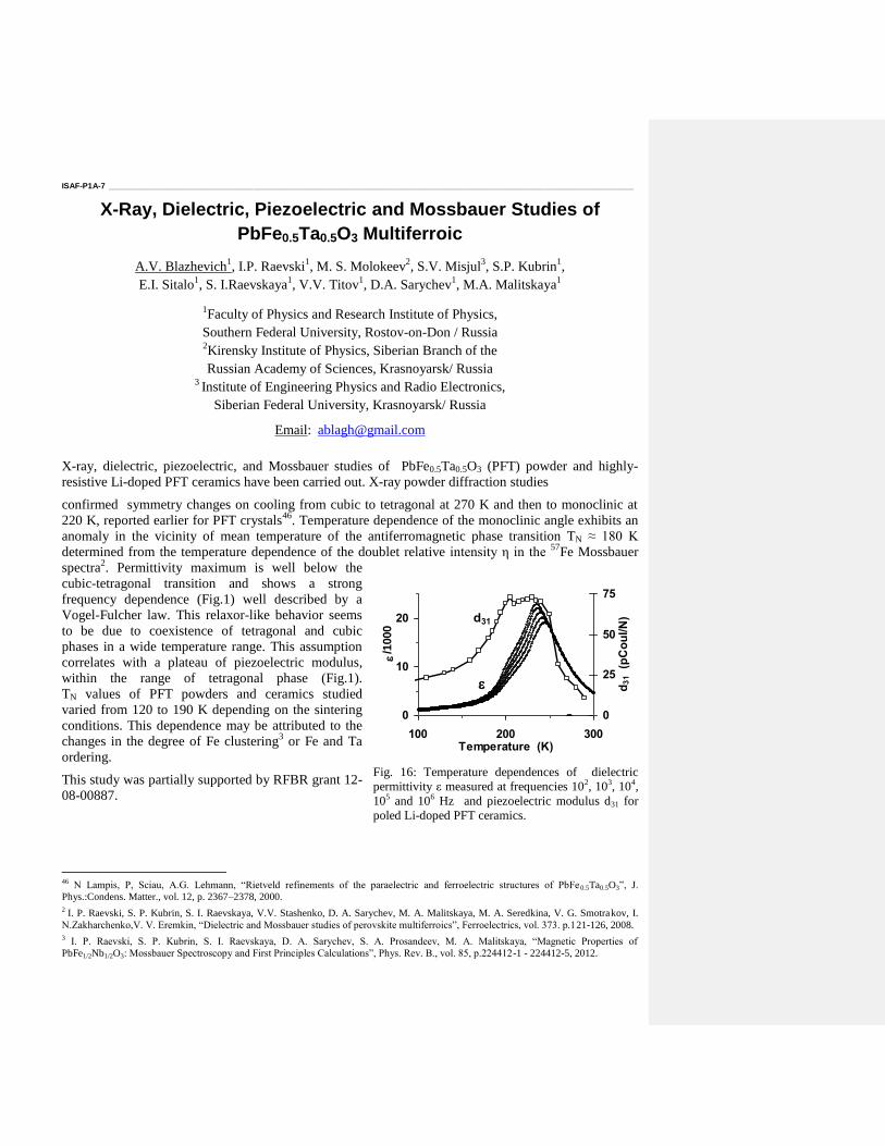
ISAF-P1A-7 ____________________________________________________________________________________________________________________
X-Ray, Dielectric, Piezoelectric and Mossbauer Studies of
PbFe0.5Ta0.5O3 Multiferroic
A.V. Blazhevich1, I.P. Raevski
1, M. S. Molokeev
2, S.V. Misjul
3, S.P. Kubrin
1,
E.I. Sitalo1, S. I.Raevskaya
1, V.V. Titov
1, D.A. Sarychev
1, M.A. Malitskaya
1
1Faculty of Physics and Research Institute of Physics,
Southern Federal University, Rostov-on-Don / Russia 2Kirensky Institute of Physics, Siberian Branch of the
Russian Academy of Sciences, Krasnoyarsk/ Russia 3
Institute of Engineering Physics and Radio Electronics,
Siberian Federal University, Krasnoyarsk/ Russia
Email: [email protected]
X-ray, dielectric, piezoelectric, and Mossbauer studies of PbFe0.5Ta0.5O3 (PFT) powder and highly-
resistive Li-doped PFT ceramics have been carried out. X-ray powder diffraction studies
confirmed symmetry changes on cooling from cubic to tetragonal at 270 K and then to monoclinic at
220 K, reported earlier for PFT crystals46
. Temperature dependence of the monoclinic angle exhibits an
anomaly in the vicinity of mean temperature of the antiferromagnetic phase transition TN ≈ 180 K
determined from the temperature dependence of the doublet relative intensity η in the 57
Fe Mossbauer
spectra2. Permittivity maximum is well below the
cubic-tetragonal transition and shows a strong
frequency dependence (Fig.1) well described by a
Vogel-Fulcher law. This relaxor-like behavior seems
to be due to coexistence of tetragonal and cubic
phases in a wide temperature range. This assumption
correlates with a plateau of piezoelectric modulus,
within the range of tetragonal phase (Fig.1).
TN values of PFT powders and ceramics studied
varied from 120 to 190 K depending on the sintering
conditions. This dependence may be attributed to the
changes in the degree of Fe clustering3 or Fe and Ta
ordering.
This study was partially supported by RFBR grant 12-
08-00887.
46 N Lampis, P, Sciau, A.G. Lehmann, “Rietveld refinements of the paraelectric and ferroelectric structures of PbFe 0.5Ta0.5O3”, J.
Phys.:Condens. Matter., vol. 12, p. 2367–2378, 2000.
2 I. P. Raevski, S. P. Kubrin, S. I. Raevskaya, V.V. Stashenko, D. A. Sarychev, M. A. Malitskaya, M. A. Seredkina, V. G. Smotrakov, I.
N.Zakharchenko,V. V. Eremkin, “Dielectric and Mossbauer studies of perovskite multiferroics”, Ferroelectrics, vol. 373. p.121-126, 2008.
3 I. P. Raevski, S. P. Kubrin, S. I. Raevskaya, D. A. Sarychev, S. A. Prosandeev, M. A. Malitskaya, “Magnetic Properties of
PbFe1/2Nb1/2O3: Mossbauer Spectroscopy and First Principles Calculations”, Phys. Rev. B., vol. 85, p.224412-1 - 224412-5, 2012.
0
10
20
100 200 300Temperature (K)
/1
000
0
25
50
75
d3
1 (p
Co
ul/N
) d31
Fig. 16: Temperature dependences of dielectric
permittivity ε measured at frequencies 102, 10
3, 10
4,
105 and 10
6 Hz and piezoelectric modulus d31 for
poled Li-doped PFT ceramics.
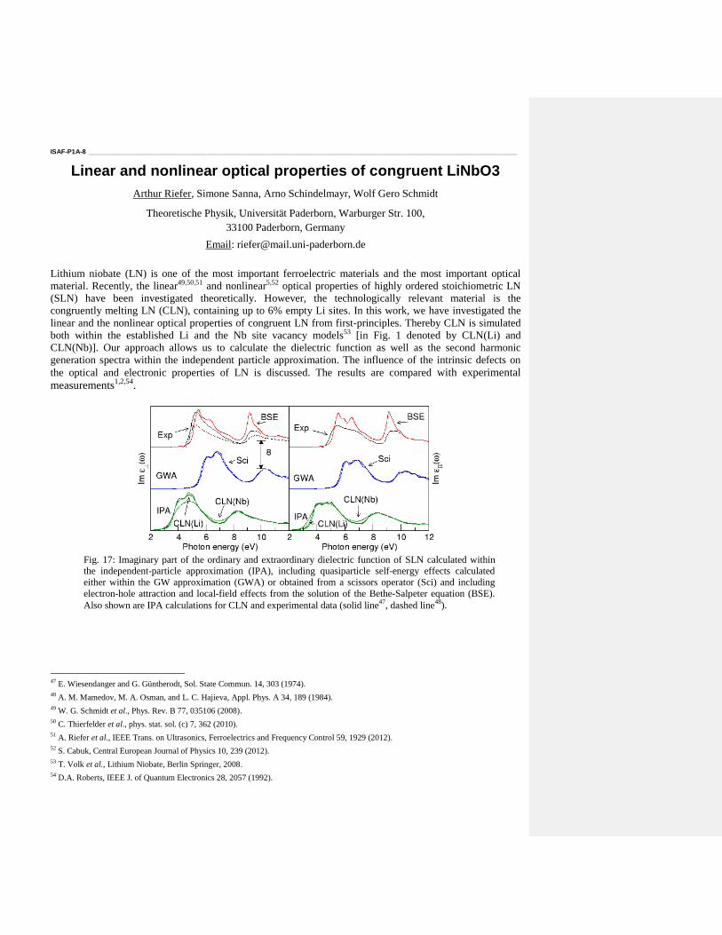
ISAF-P1A-8 ____________________________________________________________________________________________________________________
Linear and nonlinear optical properties of congruent LiNbO3
Arthur Riefer, Simone Sanna, Arno Schindelmayr, Wolf Gero Schmidt
Theoretische Physik, Universität Paderborn, Warburger Str. 100,
33100 Paderborn, Germany
Email: [email protected]
Lithium niobate (LN) is one of the most important ferroelectric materials and the most important optical
material. Recently, the linear49,50,51 and nonlinear5,52 optical properties of highly ordered stoichiometric LN
(SLN) have been investigated theoretically. However, the technologically relevant material is the
congruently melting LN (CLN), containing up to 6% empty Li sites. In this work, we have investigated the
linear and the nonlinear optical properties of congruent LN from first-principles. Thereby CLN is simulated
both within the established Li and the Nb site vacancy models53 [in Fig. 1 denoted by CLN(Li) and
CLN(Nb)]. Our approach allows us to calculate the dielectric function as well as the second harmonic
generation spectra within the independent particle approximation. The influence of the intrinsic defects on
the optical and electronic properties of LN is discussed. The results are compared with experimental
measurements1,2,54
.
47 E. Wiesendanger and G. Güntherodt, Sol. State Commun. 14, 303 (1974).
48 A. M. Mamedov, M. A. Osman, and L. C. Hajieva, Appl. Phys. A 34, 189 (1984).
49 W. G. Schmidt et al., Phys. Rev. B 77, 035106 (2008).
50 C. Thierfelder et al., phys. stat. sol. (c) 7, 362 (2010).
51 A. Riefer et al., IEEE Trans. on Ultrasonics, Ferroelectrics and Frequency Control 59, 1929 (2012).
52 S. Cabuk, Central European Journal of Physics 10, 239 (2012).
53 T. Volk et al., Lithium Niobate, Berlin Springer, 2008.
54 D.A. Roberts, IEEE J. of Quantum Electronics 28, 2057 (1992).
Fig. 17: Imaginary part of the ordinary and extraordinary dielectric function of SLN calculated within
the independent-particle approximation (IPA), including quasiparticle self-energy effects calculated
either within the GW approximation (GWA) or obtained from a scissors operator (Sci) and including
electron-hole attraction and local-field effects from the solution of the Bethe-Salpeter equation (BSE).
Also shown are IPA calculations for CLN and experimental data (solid line47
, dashed line48
).
ISAF-P1A-9 ____________________________________________________________________________________________________________________
Dynamic Denisyuk holograms in photorefractive crystals:
fundamental physical properties and applications for
interferometry
Pavel V. Zuev1, Stanislav M. Shandarov
1, Sergey S. Shmakov
1, Nikolay I. Burimov
1, Vitaly I.
Bykov1, Alexander E. Urban, Yury F. Kargin
2, Vasiliy V. Shepelevich
3
1Department of Electronic Devices, Tomsk State University of Control System and
Radioelectronics, Tomsk 634050, Russia 2Baikov Institute of Metallurgy and Materials Science Sciences of the RAS, Moscow
119991, Russia 3Department of Theoretical Physics, I.P. Shamyakin Mozyr State Pedagogical University, Mozyr
247760, Belarus
Email: [email protected]
We report on adaptive interferometry based on dynamic reflection holograms in photorefractive crystals. The
basic physical principles of the interaction of two counterpropagating light waves on dynamic reflection
gratings formed in the Denisyuk scheme in photorefractive crystals due to the diffusion mechanism of the
charge transfer are considered. We analyze the nonlinear response relating to both phase (photorefractive)
and amplitude (absorption) components of the reflection grating. Along with conventional linear electro-
optic effect the additional elasto-optic contributions to the phase grating induced by secondary phenomena
are taken into account. We consider two converse effects, piezoelectric and flexoelectric ones, as the causes
of existence of the elastic-strain gratings in the electro-optic (photorefractive) crystals.
The peculiarity of reflection volume holograms, which formed by interaction of waves from visible region, is
the small spatial period assuming values about 100 nm55. In this case the reflection holograms are
accompanied by electric-field gradient may be as high as several TV/m2. It is shown that owing to converse
flexoelectric effect, these giant gradient values are capable of generation in photorefractive crystal the
appreciable elastic strains. We have considered the contradirectional interaction between a strong stationary
reference wave and a weak phase-modulated signal wave on a reflection grating in the X-cut piezoelectric
(electro-optic) crystals belonging to the point symmetry groups 23, 43m , 42m , 422, 622, and 222. . It was
shown that qualitative distinctions in photorefractive response induced by linear electro-optic effect and by
converse flexoelectric effect together with the elasto-optic one are exhibited at phase demodulation in an
adaptive interferometric setup utilizing interaction of two counterpropagating light beams on the reflection
holograms. Based on the experiments with such interaction in the (100)-cut Bi12TiO20:Fe,Cu crystals we
established that theirs flexoelectric coefficient f11 can be estimated as the value in the range from 1.9 to 5.3
nC/m2.
This work was supported in part by the Russian Foundation for Basic Research (grant No 12-02-
90038_Bel_а), and by the Belarusian Republican Foundation for Fundamental Research (grant No F12R-
222).
55
S.M. Shandarov, S.S. Shmakov, N.I. Burimov, O.S. Syuvaeva, Yu.F. Kargin, and V.M. Petrov, “Detection of the
contribution of the inverse flexoelectric effect to the photorefractive response in a bismuth titanium oxide single crystal,”
JETP Letters, vol. 95, p. 699–702, 2012.
ISAF-P1A-10 ___________________________________________________________________________________________________________________
Modeling of switching and piezoelectric phenomena in PVDF
Vladimir Bystrov1,2
, Ekaterina Paramonova2, Varsenik Gevorkyan
3, Leon Avakyan
3, Igor Bdikin
4,
Robert Pullar1 and Andrei Kholkin
1
1Department Materials Eng. and Ceramics & CICECO, University of Aveiro, Aveiro, Portugal
2Institute of Mathematical Problems of Biology, Rus. Academy of Sciences, Pushchino, Russia
3Physics Faculty, Southern Federal University, Rostov-on-Don, Russia
4Centre for Mechanical Technology and Automation, University of Aveiro, Aveiro, Portugal
Email: [email protected] , [email protected]
At the present work we consider the molecular model of ferroelectric polymer polyvinylidene fluoride
(PVDF) film, consisting from one, two chains [-CH2-CF2-]n and for PVDF unit cell. The main software was
HyperChem 8.0 for all models as for quantum calculations as well for molecular mechanics. First principle
calculations were employed, using various quantum-chemical methods (QM), including semi-empirical
(PM3) and various density functional theory (DFT) approaches, and in addition combined with molecular
mechanics (MM) methods in complex joint approaches (QM/MM). The first model, is limited by n= 6
elementary units CH2CF2. The first principle approach PM3 and molecular dynamic run were applied for
investigation of the switching and its kinetics for these models. It is revealed, that kinetics of polarization
switching shows a homogeneous critical behavior with critical point at Landau-Ginzburg-Devonshire (LGD)
coercive field E = EC. Two types of 2 PVDF chains behavior were established: simultaneous and
consequence rotation in low and high electric field for two chains model. Our modeling and first principle
calculation for one chain model was obtained hysteresis loop for PVDF with LGD intrinsic coercive field EC
~ 1 GV/m and for two chains it is confirmed with EC ~ 2…2.5 GV/m. These obtained results are compared
with experimental data at the nano-scale level by the atomic force microscopy. These data are related also
with arisen of the PVDF piezoelectric effects, especially of the negative piezoelectric coefficients. Performed
detailed molecular modeling was applied to study the nature of this negative piezoelectric effect in PVDF,
and these results confirmed by actual nanoscale measurements. Both PVDF molecular chains and a unit cell
of crystalline -phase PVDF were modelled. This computational molecular exploration clearly shows that
the nature of the so-called negative piezo-electric effect in the ferroelectric PVDF polymer has a self-
consistent quantum nature, and is related to the redistribution of the electron molecular orbitals (wave
functions), leading to the shifting of atomic nuclei and reorganization of all total atomic charges to the new,
energetically optimal positions, under an applied electrical field. As a results, complex cooperative dipole
reorganization occurs on the bonded molecular chain under the action of this applied electrical field.
Complicated non-uniform and nonlinear anisotropy deformations in the PVDF molecular chain result,
involving both individual interactions of C2H2F2 dipoles, as well as the whole PVDF unit cell, leading to
negative deformation in relation to the applied field. Molecular modeling and first principles calculations
show that the piezoelectric coefficient d33 has negative values in the range d33 ~-16.5…-33.5 pC/N (pm/V),
corresponding to known data, and allowing us to explain the reasons for the negative sign of the piezo-
response. For value of we obtained a value of another oriented coefficient d31 ~ +15.5 pC/N (with a
positive sign). This computational study is corroborated by measured nanoscale data obtained by atomic
force and piezo-response force microscopy (AFM / PFM). This study could be useful as a basis for further
insights into organic and molecular ferroelectrics.
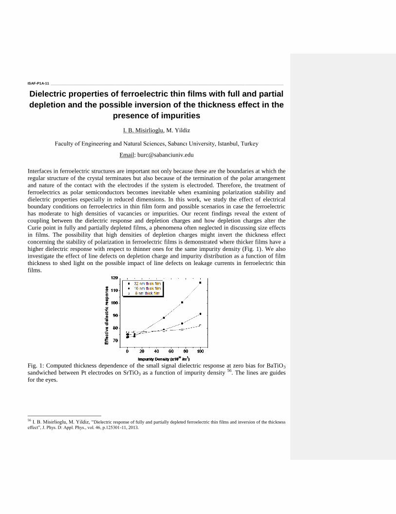
ISAF-P1A-11 ___________________________________________________________________________________________________________________
Dielectric properties of ferroelectric thin films with full and partial
depletion and the possible inversion of the thickness effect in the
presence of impurities
I. B. Misirlioglu, M. Yildiz
Faculty of Engineering and Natural Sciences, Sabancı University, Istanbul, Turkey
Email: [email protected]
Interfaces in ferroelectric structures are important not only because these are the boundaries at which the
regular structure of the crystal terminates but also because of the termination of the polar arrangement
and nature of the contact with the electrodes if the system is electroded. Therefore, the treatment of
ferroelectrics as polar semiconductors becomes inevitable when examining polarization stability and
dielectric properties especially in reduced dimensions. In this work, we study the effect of electrical
boundary conditions on ferroelectrics in thin film form and possible scenarios in case the ferroelectric
has moderate to high densities of vacancies or impurities. Our recent findings reveal the extent of
coupling between the dielectric response and depletion charges and how depletion charges alter the
Curie point in fully and partially depleted films, a phenomena often neglected in discussing size effects
in films. The possibility that high densities of depletion charges might invert the thickness effect
concerning the stability of polarization in ferroelectric films is demonstrated where thicker films have a
higher dielectric response with respect to thinner ones for the same impurity density (Fig. 1). We also
investigate the effect of line defects on depletion charge and impurity distribution as a function of film
thickness to shed light on the possible impact of line defects on leakage currents in ferroelectric thin
films.
Fig. 1: Computed thickness dependence of the small signal dielectric response at zero bias for BaTiO3
sandwiched between Pt electrodes on SrTiO3 as a function of impurity density 56
. The lines are guides
for the eyes.
56
I. B. Misirlioglu, M. Yildiz, “Dielectric response of fully and partially depleted ferroelectric thin films and inversion of the thickness
effect”, J. Phys. D: Appl. Phys., vol. 46, p.125301-11, 2013.
ISAF-P1A-12 ___________________________________________________________________________________________________________________
Influence of the piezoelectric effect on
ferroelectric properties and phase transition Andreas Leschhorn
1 , Herbert Kliem
1
1Institute of Electrical Engineering Physics, Saarland University, Saarbruecken, Germany
Email: [email protected]
The Weiss model for magnetization can also be applied to the polarization of ferroelectrics57
. In this
model, the local field is the superposition of the applied field Ea and of a field proportional to the
polarization P:
(1)
The coupling parameter α describes the coupling between the dipoles by the electrostatic fields. The
dipoles with moment p are assumed to fluctuate thermally activated in double well potentials yielding
(temperature T, dipole density n)
(
) (2)
With (1) and (2) we have a feedback loop for the polarization. In this form the model predicts several
properties of ferroelectric materials like the polarization hysteresis and the phase transition from
ferroelectric to paraelectric at the Curie temperature. However, the model only yields a ferro- to
paraelectric transition of the second type.
The type 2 transition can be converted into a type 1 transition by introducing the piezoelectric effect58
.
Simultaneously the single hysteresis of polarization splits into a double hysteresis loop close to the Curie
point.
With the piezoelectric effect the distances inside the sample depend on the polarization. In this way
some parameters in (1) and (2) are functions of P, namely the dipole moment p, the density n and the
coupling parameter α. If the length of the sample is changed due to the polarization the distances
between the dipoles are altered and e.g. the coupling constant α is also varied like (piezo coefficient
ς)
( ) ( ) (3)
Combining (1), (2) and (3) yields the ferro- to paraelectric transition of the first order. In an analogous
way also the variation of p and/or n with the polarization P can cause this change from type 2 to type 1
transition.
Acknowledgement: This work is supported by the Deutsche Forschungsgemeinschaft.
57 J. C. Burfoot , G. W. Taylor, “Polar Dielectrics”, MacMillan Press, London, 1979.
58 H. Kliem, , “Strain induced change from second order to first order ferroelectric phase transition”, Ferroelectrics,
vol. 425, p. 54-62, 2011.
ISAF-P1A-13 ___________________________________________________________________________________________________________________
Modeling and Numerical Study of Electroacoustic Behavior of
Lithium Niobate Under an Initial Electrical Stress
Domenjoud Mathieu1, Lematre Michaël
2, Fortineau
Jérôme
2, Feuillard Guy
2 and Tran-Huu-Hue Louis-
Pascal2
1GREMAN, UMR CNRS 7347, University of Tours, Tours, France
2GREMAN, UMR CNRS 7347, ENIVL, Blois, France
Email: [email protected]
Piezoelectric materials are frequently used for various applications, such as sensors, actuators or
transducers, many of which imply operation under harsh environmental conditions like high
temperature, high pressure, external electrical DC bias field or mechanical stress. For instance, Tonpilz
piezoelectric transducers are built in such a way that a stress-bolt assembly maintains the piezoelectric
stacks under compression, leading to an increased efficiency and lifetime. Conversely, in high power
ultrasonic transducers used for therapy, the electroacoustic response can be improved by applying a
static electrical field. However, the presence of high external (mechanical or electrical) stress induces
non-linear effects that significantly modify the piezoelectric characteristics through a shift of material
properties from their stress-free values. The improvement of electromechanical performance due to
external prestress is not very well known and designers of systems, who have to deal with difficulties to
evaluate piezoelectric material properties in real operating conditions, often rely on empirical
considerations.
Recently, we developed a second order formalism of piezoelectric structures under an external
(mechanical or electrical) stress in the natural (nondeformed) and current (predeformed) coordinate
systems59
. Here, our formalism is used to evaluate the effect of an applied electrical stress on the
electroacoustic behavior of piezoelectric materials. Knowing the coercitive field of lithium niobate
material, we numerically quantify nonlinearities induced by an electrical prestress on the deformations,
wave velocities and coupling coefficients for a lithium niobate plate. Evolutions of these parameters are
studied in the two coordinate systems as a function of the azimuthal and elevation angles as well as
electrical prestress values.
We show that the contribution of nonlinearity to deformation reaches 22.5% in a specific cut
plane. Moreover, the maximum shift in wave velocities induced by prestress is found to be 33 and 9 m/s
for quasi-longitudinal and quasi-transversal modes respectively. Numerical studies of electromechanical
coupling coefficients show that the electrical prestress is able to produce an increase of about +1.1%.
Finally, we show that electrical prestress in specific cut planes significantly increases longitudinal wave
velocities and electromechanical coupling coefficients. This study shows that, by designing an electrical
prestressed transducer using a piezoelectric material in well determined cuts, it is possible to increase the
performance and that this can be predicted.
59
M. Lematre, M. Domenjoud and L. P. Tran-Huu-Hue, “Exact second order formalism for the study of electro-acoustic
properties in piezoelectric structure under an initial mechanical stress”, Ultrasonics, vol. 51, p 898-910, 2011.
ISAF-P1A-14 ___________________________________________________________________________________________________________________
The abnormal polarization switching of relaxor terpolymer films at low
temperature
B. B. Tian, X. L. Zhao, B. L. Liu, J. L. Wang, J. L. Sun, X. J. Meng and J. H. Chu
1State Key Laboratory of Infrared Physics, Shanghai Institute of Technical Physics, Chinese Academy
of Sciences, Yu Tian Road 500, Shanghai 200083, China
Abstract
The ferroelectricity of the Poly(vinylidene fluoride-trifluoroethylene-chlorofloroethylene) terpolymer
films fabricated by the Langmuir–Blodgett (LB) technology were investigated from 180 to 300 K. The
temperature dependence of the remanent polarization and the dielectric response shows a broad peak at
~ 270 K, suggesting a ferroelectric phase transition. Contrary to the perovskite relaxor, a deviation from
the Merz’s law is observed in the relation between the coercive field and frequency for the relaxor
terpolymer. The particular ferroelectricity of the relaxor terpolymer is considered to be associated with
the distinct structure and the dynamics of its typical molecular conformations.
ISAF-P1A-15 ___________________________________________________________________________________________________________________
Effect of grain size on the microwave dielectric properties of β-
BZN ceramics
Gao-qun Zhang1, Hong Wang
1, Di Zhou
1, Jing Guo
1
1Electronic Materials Research Laboratory, Key Laboratory of Ministry of Education,
Xi’an Jiaotong University, Xi’an 710049, China
Email: [email protected]
In this study, β-BZN ceramics were prepared by the traditional solid state method. The samples sintered
at 930 oC for 2 h possessed a relative permittivity of 74 and a Q×f value of 3740 GHz. The grain size of
β-BZN ceramics was regulated by changing sintering temperature and heat preservation time. When the
sintering temperature was increased from 780 oC to 990
oC, the grain grew from 0.7 um to 1.9 um as
approximate exponential function. Grain growth mechanism of β-BZN ceramic with sintering
temperature was discussed. The function
310003ln 1000 3T
pl t e
about the relationship between the grain size of β-BZN and sintering temperature was obtained by
simulation, whose results were in accord with experimental values. For the samples at different heat
preservation time, there was deviation between experimental values and results from theory model
formula
2 2
0G G Ct .
For well dense β-BZN, the grain size has little effect on the relative permittivity. And the Q×f value
increased with increasing grain size from 0.7 um to 1.2 um, but for β-BZN ceramics of the average grain
size above 1.2 um, the Q×f value decreased. When the grains grew from 0.7 um to 1.2 um, there was a
uniform microstructure, and a reduction in the number of grain boundaries per unit volume would result
in material with a lower loss. When the average size of the grains was more than 1.2 um, some large
grains appeared, which introduced more defect and deteriorated the quality factor.
ISAF-P1A-16 ___________________________________________________________________________________________________________________
Density Functional Theory Calculations of Doped
Perovskite Barium Titanate (BaTi0.6Nb0.2Fe0.1O3): Structural
Deformations and Ferroelectric Properties
Piyarat Nimmanpipug1,2
, Wiranwit Wankawee1, Laongnuan Srisombat
1,2, Yongyut
Laosiritaworn1,2
1Computational Simulation and Modelling Laboratory (CSML), Department of Chemistry, Faculty
of Science, Chiang Mai University, Chiang Mai 50200, Thailand
2Thailand Center of Excellence in Physics (ThEP), Commission on Higher Education, Bangkok
10400, Thailand
Email: [email protected], [email protected]
The structural deformations and ferroelectric properties of doped barium titanate were theoretically
analyzed using density functional theory (DFT). Niobium (Nb5+
) and ferrous (Fe2+
) ion were substituted
in all possible titanium sites to evaluate all possible structures. The distortion of octahedral hole was
found depending on size of dopant and neighboring atoms. The direction of atomic displacement in
octahedral holes were investigated and related to the direction of polarization. The splitting of phonon
modes was observed in doped barium titanate indicating ferroelectric instability of the structure. The
electronic band structure and density of states (DOS) indicate decrease of energy band gap in doped
structures. The hybridization of the Ti-3d, Nb-4d and Fe-3d with the O-2p orbitals was remarked
corresponding with the shift in the frequency of phonon modes.
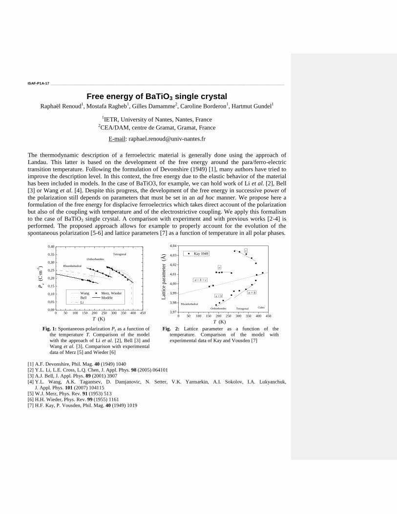
ISAF-P1A-17 ___________________________________________________________________________________________________________________
Free energy of BaTiO3 single crystal Raphaël Renoud
1, Mostafa Ragheb
1, Gilles Damamme
2, Caroline Borderon
1, Hartmut Gundel
1
1IETR, University of Nantes, Nantes, France
2CEA/DAM, centre de Gramat, Gramat, France
E-mail: [email protected]
The thermodynamic description of a ferroelectric material is generally done using the approach of
Landau. This latter is based on the development of the free energy around the para/ferro-electric
transition temperature. Following the formulation of Devonshire (1949) [1], many authors have tried to
improve the description level. In this context, the free energy due to the elastic behavior of the material
has been included in models. In the case of BaTiO3, for example, we can hold work of Li et al. [2], Bell
[3] or Wang et al. [4]. Despite this progress, the development of the free energy in successive power of
the polarization still depends on parameters that must be set in an ad hoc manner. We propose here a
formulation of the free energy for displacive ferroelectrics which takes direct account of the polarization
but also of the coupling with temperature and of the electrostrictive coupling. We apply this formalism
to the case of BaTiO3 single crystal. A comparison with experiment and with previous works [2-4] is
performed. The proposed approach allows for example to properly account for the evolution of the
spontaneous polarization [5-6] and lattice parameters [7] as a function of temperature in all polar phases.
0 50 100 150 200 250 300 350 400 4500,00
0,05
0,10
0,15
0,20
0,25
0,30
0,35
0,40
Rhombohedral
Orthorhombic
Pz
(C·m
-2)
T (K)
Wang Merz, Wieder
Bell Modèle
Li
Tetragonal
0 50 100 150 200 250 300 350 400 450
3,97
3,98
3,99
4,00
4,01
4,02
4,03
4,04
Lat
tice
par
amet
er
(Å)
T (K)
CubicTetragonalOrthorhombic
Rhombohedral
c
a = b = c
a = b
a = b
c
Kay 1949
Fig. 1: Spontaneous polarization Pz as a function of
the temperature T. Comparison of the model
with the approach of Li et al. [2], Bell [3] and
Wang et al. [3]. Comparison with experimental
data of Merz [5] and Wieder [6]
Fig. 2: Lattice parameter as a function of the
temperature. Comparison of the model with
experimental data of Kay and Vousden [7]
[1] A.F. Devonshire, Phil. Mag. 40 (1949) 1040
[2] Y.L. Li, L.E. Cross, L.Q. Chen, J. Appl. Phys. 98 (2005) 064101
[3] A.J. Bell, J. Appl. Phys. 89 (2001) 3907
[4] Y.L. Wang, A.K. Tagantsev, D. Damjanovic, N. Setter, V.K. Yarmarkin, A.I. Sokolov, I.A. Lukyanchuk,
J. Appl. Phys. 101 (2007) 104115
[5] W.J. Merz, Phys. Rev. 91 (1953) 513
[6] H.H. Wieder, Phys. Rev. 99 (1955) 1161
[7] H.F. Kay, P. Vousden, Phil. Mag. 40 (1949) 1019
ISAF-P1A-18 ___________________________________________________________________________________________________________________
Ferroelectric domain engineering in tricolour superlattices
C. Hubault1,5
, I. C. Infante2, A. Boulle
3, N. Boudet
4,C. Davoisne
5, L. Dupont
5, V. Demange
6, A. Perrin
6,
B. Gautier7, M.G. Karkut
1 and N. Lemée
1*
1LPMC, Université de Picardie Jules Verne, Amiens, France
2SPMS, CNRS UMR 8580, Ecole Centrale Paris, France
3SPCTS, CNRS UMR 7315, Limoges, France
4D2AM-CRG, ESRF and Institut Néel, CNRS, Grenoble, France
5LRCS, CNRS UMR 7314, Amiens, France
6USCR, CNRS UMR 6226, Rennes, France
7INL, CNRS UMR 5270, INSA, Villeurbanne, France
Email: [email protected]
Functional properties of perovskite ferroelectric thin films are highly influenced by their domain
structure which is determined both by epitaxial strain and depolarizing fields. Ferroelectric superlattices
can provide a way to disentangle the competition between the elastic and electrostatic energy. Recently
we have applied tensile in-plane strain to PbTiO3 (PT) by combining PT, PbZr0.2Ti0.8O3 (PZT 20-80) and
SrTiO3 (STO) in tricolour superlattices60
. In bicolour PT/PZT 20-80 SLs, an a/c polydomain structure
was evidenced61
. In tricolor PT/STO/PZT superlattices, the introduction of ultrathin layers of STO (2-3
unit cells) between each ferroelectric layer seems to play a significant role in the decoupling of
ferroelectric interactions. Indeed, the insertion of STO layers induces a strong decrease in the
tetragonality of the overall superlattice, and inhibits this 90° polydomain formation. X-ray diffraction
measurements evidence the presence of satellites around the out-of-plane SL Bragg peaks. This
modulation is characteristic of 180° ferroelectric domains of alternate “up” and “down” polarization,
presumably produced to minimize the electric field arising from the STO induced depolarizing field.
Their polar origin is clearly confirmed by their disappearance close to the superlattice ferroelectric
transition temperature. In order to investigate the in-plane polar structure, reciprocal space maps were
realized using grazing incidence diffraction at beamline BM2-D2AM at ESRF. The period of the
observed satellites is consistent with the polar modulation measured around the specular reflections.
These measurements show that in the tricolour PT/STO/PZT 20-80 superlattices the polarization has
both in-plane and out-of-plane components, which is an argument in favour of a polarization rotation
away from the normal. Using piezo-force microscopy, it is possible to write and image polarization
domains, confirming that the piezoelectric response of the sample is still retained with the 180°
nanodomain formation. This work demonstrates that such tricolour ferroelectric superlattices provide a
powerful tool to study the role of electrostatic and strain effects in the control of polarization orientation.
60
C. Hubault et al., J. Appl. Phys., vol. 112, 114102, 2012 61
C. Hubault et al., Appl. Phys. Lett., vol. 99, 052905, 2011
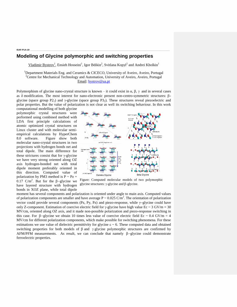
ISAF-P1A-19 ___________________________________________________________________________________________________________________
Modeling of Glycine polymorphic and switching properties
Vladimir Bystrov1, Ensieh Hosseini
1, Igor Bdikin
2, Svitlana Kopyl
2 and Andrei Kholkin
1
1Department Materials Eng. and Ceramics & CICECO, University of Aveiro, Aveiro, Portugal 2Centre for Mechanical Technology and Automation, University of Aveiro, Aveiro, Portugal
Email: [email protected]
Polymorphism of glycine nano-crystal structure is known – it could exist in and in several cases
as modification. The most interest for nano-electronic present non-centro-symmetric structures: -
glycine (space group P21) and -glycine (space group P32). These structures reveal piezoelectric and
polar properties. But the value of polarization is not clear as well its switching behaviour. In this work
computational modelling of both glycine
polymorphic crystal structures were
performed using combined method with
LDA first principle calculations of
atomic optimized crystal structures on
Linux cluster and with molecular semi-
empirical calculations by HyperChem
8.0 software. Figure show both
molecular nano-crystal structures in two
projections with hydrogen bonds net and
total dipole. The main difference for
these strictures consist that for -glycine
we have very strong oriented along OZ
axis hydrogen-bonded net with total
dipole moment preferably oriented in
this direction. Computed value of
polarization by PM3 method is P ~ Pz =
0.17 C/m2. But for the glycine we
have layered structure with hydrogen
bonds in XOZ plane, while total dipole
moment has several components and polarization is oriented under angle to main axis. Computed values
of polarization components are smaller and have average P ~ 0.025 C/m2. The orientation of polarization
vector could provide several components (Pz, Py, Pz) and piezo-response, while glycine could have
only Z-component. Estimation of coercive electric field for -glycine have high value Ec ~ 3 GV/m = 30
MV/cm, oriented along OZ axis, and it made non-possible polarization and piezo-response switching in
this case. For glycine we obtain 10 times less value of coercive electric field Ec ~ 0.4 GV/m = 4
MV/cm for different polarization components, which make possible for switching phenomena. For these
estimations we use value of dielectric permittivity for glycine ~ 6. These computed data and obtained
switching properties for both models of and glycine polymorphic structures are confirmed by
AFM/PFM measurements. As result, we can conclude that namely glycine could demonstrate
ferroelectric properties.
Figure: Computed molecular models of two polymorphic
glycine structures:-glycine and -glycine.
ISAF-P1A-20 ___________________________________________________________________________________________________________________
Domain Kinetics in Lithium Niobate Single Crystals
Inhomogeneously Modified by Annealing in Vacuum
Alikin Denis, Pryakhina Victoria, Shur Vladimir, Negashev Stanislav, Palitsin Ilya
Ferroelectric laboratory, Institute of the Natural Science, Ekaterinburg, Russia
Email: [email protected]
It is known that annealing of the lithium niobate (LN) crystals in vacuum leads to sufficient increase of the
bulk conductivity caused by out-diffusion of oxygen ions62. We present experimental study of the
polarization reversal in the single crystalline plates of congruent LN annealed in vacuum in different
temperature-time regimes: 300oC, 1h, 300oC, 10 h and 850oC, 15 min.
The polarization reversal was carried out by
application of electric field using liquid electrolyte
(aqua solution of LiCl). Instantaneous domain
patterns were in situ visualized by polarized optical
microscope (Carl Zeiss LMA 10, Germany). The
static domain patterns revealed by chemical etching
were observed by optical microscopy.
Nondestructive high resolution domain
visualization was achieved by piezoresponse force
microscopy and Raman confocal microscopy (NT-
MDT NanoLaboratories NTEGRA Aura and
NTEGRA Spectra, Russia).
Annealing at 300oC during 1 h didn’t change the
domain kinetics remarkably. The annealing at the
same temperature during 10 h leads to domain
kinetics with formation of the residual domains and
traces of the domain walls typical for modification
of the thin surface layer 63.
Annealing at high temperature (850oC) drastically modified the domain kinetics and leads to smooth
isotropic motion of the domain walls in the bulk (Fig. 1). The stable domain structure with charged domain
walls appeared over the whole switched area. The obtained switching in the bulk and isotropic domain
growth was attributed to inhomogeneous field distribution caused by inhomogeneous bulk conductivity.
The equipment of the UCSU “Modern Nanotechnology”, Institute of Natural Sciences, UrFU has been used.
The research was made possible in part by RFBR (Grants 13-02-01391-а, 12-02-31377, 11-02-91066-CNRS-
а), by Ministry of Education and Science (Сontract 14.513.12.0006).
62 P.F. Bordui, D.H. Jundt, E.M. Standifer, R.G. Norwood, R.L. Sawin, J.D. Galipeau, “Chemically reduced lithium niobate single crystals:
Processing, properties and improved surface acoustic wave device fabrication and performance“, Appl. Phys, vol. 85, p. 3766 – 3769, 1999
63 D.O. Alikin, V.Ya. Shur, V.I. Pryakhina, N.V. Gavrilov, M. Carrascosa, J. Olivares, The Domain Kinetics in Congruent Lithium Niobate
Modified by Low and High Energy Ion Irradiation, Ferroelectrics, vol. 441, p. 17-24, 2012
Fig.1. Domain kinetics in vacuum annealed lithium
niobate (850 °C, 15 min). Time form the beginning
of the pulse: (а) 48.8 s, (b) 51.6 s, (c) 53.2 s, (d)
53.6 s.
ISAF-P1A-21 ___________________________________________________________________________________________________________________
Polarization Reversal Process in Lithium Niobate Single
Crystals with Photoresist Dielectric Layer
Shur Vladimir1,2
, Akhmatkhanov Andrey1,2
, Baturin Ivan1,2
, Zorikhin Dmitriy1,2
, Chuvakova Mariya1,
Lukmanova Almira1, Zelenovskiy Pavel
1, Neradovskiy Maxim
1.
1Ferroelectrics laboratory, Ural Federal University, Ekaterinburg, Russia
2Labfer Ltd., Ekaterinburg, Russia
Email: [email protected]
The creation of the tailored periodic domain structure in lithium niobate (LiNbO3, LN) single crystals is
widely used technique for efficient conversion of the laser light frequency based on quasi-phase-
matching effect. The regular domain structure in LN is usually created by application of inhomogeneous
external electric field through the photoresist mask using liquid electrodes. Thus the study of domain
kinetics in LN covered by photoresist film is of the great practical importance for developing the
methods of domain engineering.
The domain structure evolution during polarization reversal has been investigated in congruent LN
(CLN) single crystals covered by photoresist dielectric film. The films with thickness ranged from 0.5 to
5.5 μm of positive (AZ-series) and negative (nLOF) photoresist were spin coated on Z+ polar CLN
surface. The polarization reversal process has been studied by in situ optical visualization of the domain
kinetics and analysis of the switching current data
It was revealed that the domain structure evolution changes drastically for film thickness about 2 m. The
conventional growth of hexagonal domains by jump-like motion of the plane domain walls oriented
along Y crystallographic directions accompanied by isolated pulses of switching current was observed
for film thickness below 2 m. In contrast the continuous domain wall motion and the smooth current
shape have been revealed for film thickness above 2 m caused by formation of the isolated
nanodomains in front of the moving domain wall.
The experimental switching current data was successfully fitted by Kolmogorov-Avrami formula
modified for switching in linearly increasing electric field in finite mediaxxi
. Two stages of the switching
process representing ”continuous nucleation” and “growth only” processes revealed by fitting of the
switching current data were confirmed by in situ observation of the domain kinetics.
The complex study of the obtained static domain structures by optical, scanning probe and Raman
confocal microscopy allowed to reconstruct the unusual domain evolution scenario during polarization
reversal in CLN covered by thick photoresist film. The obtained results are important for creation of the
periodically poled CLN crystals.
The equipment of the UCSU “Modern Nanotechnology”, Institute of Natural Sciences, UrFU has been used.
The research was made possible in part by RFBR (Grants 13-02-01391-а, 11-02-91066-CNRS-а), by
Ministry of Education and Science (Сontract 14.513.12.0006), by OPTEC LLC and in terms of Ural Federal
University development program with the financial support of young scientists.
ISAF-P1A-22 ___________________________________________________________________________________________________________________
Structural, elastic, and vibrational properties of Topological Insulators
on A2 5B3
6 compound based
H. Koc
64, Amirullah M. Mamedov
2, Ekmel Ozbay
2
1 Department of Physics, Siirt University, 56100 Siirt, Turkey
2Nanotechnology Research Center (NANOTAM), Bilkent University, 06800 Bilkent, Ankara, Turkey
Email: [email protected]
We have performed a first principles study of structural and elastic properties of rhombohedral Sb2Te3
and Bi2Te3 compounds using the density functional theory within the local density approximation. The
lattice parameters, bulk modulus, and its pressure derivatives of considered compounds have been
calculated. The second-order elastic constants have been calculated, and the other related quantities such
as the Young’s modulus, shear modulus, Poisson’s ratio, anisotropy factor, sound velocities, Debye
temperature, and hardness have also been estimated in the present work. The phonon dispersion curves
are derived using the direct method. The present results demonstrate that this compound is dynamically
stable.
Fig. 1: Energy band structure for Sb2Te3 and Bi2Te3. The calculated electronic band structure shows that Sb2Te3
and Bi2Te3 compounds have an direct band gap with the value 0.093 eV and 0.099 eV, respectively.
64
H. Koc, E. Deligöz, Amirullah M. Mamedov, “The elastic, electronic, and optical properties of PtSi and PtGe compounds”
Philophical Magazine, Vol. 91, p. 3093-3107, 2011.

ISAF-P1A-23 ___________________________________________________________________________________________________________________
Linear and Non-Linear Optical Properties of AgBO3(B=Nb, Ta):
First Principle Study
Sevket Simsek, Amirullah M. Mamedov, Ekmel Ozbay
Nanotechnology Research Center (NANOTAM), Bilkent University 06800, Bilkent, Ankara, Turkey
Email: [email protected]
The linear and nonlinear optical properties of ferroelectrics AgBO3 (B=Ta, Nb) are studied by density functional
theory (DFT) in the local density approximation (LDA) expressions based on first principle calculations without
the scissor approximation. Specially, we present calculations of the frequency- dependent complex dielectric
function , and the second harmonic generation response coefficient ),,2()2( over a large frequency
range in rhombohedral phase for the first time. The electronic linear electrooptic susceptibility )0,,()2( is
also evaluated below the band gap. These results are based on a series of the LDA calculation using DFT. Our
goals are to give the details of the calculations for linear and nonlinear optical properties, including the linear
electro-optic (EO) tensor for some ABO3 structures with oxygen octahedral structures using first-principles
methods65, 66
.
65
S. Cabuk and S. Simsek, “First-principles calculation of the linear and nonlinear optical properties of LiTaO3”, Phys. Scr.,
Vol. 81, p. 055703-055710, 2010. 66
H. Akkus, Amirullah M. Mamedov, “Linear and Nonlinear Optical Properties of SbSI: First-Principle Calculation”,
Ferroelectrics, Vol. 352, p.148–152, 2007.
ISAF-P1A-24 ___________________________________________________________________________________________________________________
One and Two-Dimensional Ferroelectric LiNbO3 Photonic Crystal Sevket Simsek, Amirullah M.Mamedov, Ekmel Ozbay
Nanotechnology Research Center (NANOTAM), Bilkent University 06800, Bilkent, Ankara, Turkey
Email: [email protected]
In this report, we present an investigation of the optical properties and band structure calculations for the
photonic crystal structures (PCs) based on one-dimensional (1D) and two-dimensional (2D) ferroelectric
LiNbO3 crystal67
. Here we use 1D and 2D periodic crystal structure of dielectric rods and layers in air
background. We have theoretically calculated photonic band structure and optical properties of 1D and
2D LiNbO3 PCs. Beside, we have calculated affect PBG properties of different parameters such as
filling fraction and the shape. In order to get photonic gap map, we have calculated the gaps as a
function of radius of the rods. We have also investigated the nature of guided modes in line defect
waveguide. In our simulation, we employed the finite-difference time domain (FDTD) technique which
implies the solution of Maxwell equations with centered finite-difference expressions for the space and
time derivatives. FDTD schemes are especially promising for the investigation of PBG structures, as
they provide an opportunity of analyzing the spatial distribution of the electromagnetic field in PBG
structure.
67
S. Simsek, Amirullah M. Mamedov, E. Ozbay “Two-Dimensional Ferroelectric Photonic Crystals: Optics and Band
Structure”, Ferroelectrics (in pres: accepted for publ).
ISAF-P1A-25 ___________________________________________________________________________________________________________________
Lattice Dynamics of Alkali Halides in the Anharmonic Regime
M. Kempa1, J. Hlinka
1, P. Ondrejkovic
1, P. Marton
1
1 Department of Dielectrics, Institute of Physics AS CR, Prague, Czech Republic
Email: [email protected]
Simple alkali halides, such as NaI or KBr, have been model examples of ionic crystals for decades,
being studied both experimentally and theoretically. Recently, renewed interest in dynamics of alkali
halides appeared: Among others, incorporation of three-body interactions into the polarizable shell
model has been shown to improve considerably the agreement between lattice dynamic calculations and
experimental results on phonon dispersion68
. Furthermore, an intrinsic localized mode (breather) was
discovered in the phonon gap of NaI doped by Tl [2] at high temperatures. Breathers can be regarded as
dynamic nanoclusters, they have been discussed in the context of relaxors3,4
, and it would be very
interesting to observe them in simple systems. Such an anharmonic lattice mode could be the same as
the locally excited vibrational mode that causes photoluminescence quenching in alkali halides doped by
ns2 ions
5,6, and had been theoretically predicted
7, but never experimentally observed before in such a
simple structure.
In this contribution, we present our inelastic neutron scattering data on both pure and doped KBr and
NaI, at room and high temperatures, as well as our first-principles calculations based on density
functional theory within the local-density approximation. The position and size of the energy gap in the
phonon density of states in a wide range of temperatures from 10 to 700 K are discussed in connection
with a pronounced temperature effect which effectively leads to closure of the phonon gap at high
temperatures8. The results are also discussed in the context of studies of possible intrinsic localized
modes in the phonon gap of alkali halides. We have also attempted to induce the anharmonic lattice
modes at low temperatures by UV excitation of the impurity electronic states of Tl+ substitution
centers9.
68
U.C. Srivastava, R.S. Pandey, K.S. Upadayaya, Int. J. Phys. Sci. 5, 972 (2010). 2 M.E. Manley, A.J. Sievers, J.W. Lynn, S.A. Kiselev, N.I. Agladze, Y. Chen, A. Llobet, A. Alatas, Phys. Rev. B 79, 134304
(2009). 3 A. Bussmann-Holder, A. R. Bishop, J. Phys.: Condens. Matter 16, L313 (2004).
4 A. Bussmann-Holder, A. R. Bishop, T. Egami, Europhys. Lett., 71, 249 (2005).
5 J. Hlinka, E. Mihokova, M. Nikl, Physica Status Solidi (b) 166, 503 (1991).
6 E. Mihokova, L.S. Schulman, J. Phys. A: Math. Theor. 43, 183001 (2010).
7 S.A. Kiselev, A.J. Sievers, Phys. Rev. B 55, 5755 (1997).
8 M. Kempa, P. Ondrejkovic, P. Bourges, J. Ollivier, S. Rols, J. Kulda, S. Margueron, J. Hlinka, J. Phys.: Condens. Matter
25, 055403 (2013). 9 M. Kempa, P. Ondrejkovic, J. Ollivier, S. Rols, J. Kulda, S. Margueron, M. Fernandez, J. Hlinka, Ferroelectrics 440, 42
(2012).
ISAF-P1A-26 ___________________________________________________________________________________________________________________
Electrical properties of ferroelectric composites described in terms of local field
inhomogeneity
L. Padurariu1 and L. Mitoseriu
1
1Faculty of Physics, Alexandru Ioan Cuza University, 11 Bv. Carol I, 700506 Iasi, Romania
In last years, the material scientists attention was focused in investigation of new dielectric
materials with tailored properties: permittivity, tunability, P(E), etc. for specific applications.
Unfortunately, the required electrical properties are not usually accomplished in single phase systems,
and the solution was the development of multiphase composite materials. By comparison with a single
phase material, a composite is characterized by the presence of interfaces separating regions with
different permittivities, which induce the formation of local inhomogeneous fields which should be
taken into account when a theoretical model is proposed.
The aim of this work is the theoretical investigation of the role of the local electric field
inhomogeneity on different electric properties of composites: effective permittivity, nonlinear tunability
and P(E) response. The local field calculations were performed by Finite Element Method (FEM), by
solving the Laplace's equation: 0 V , where is the local permittivity, V is the local potential
and the local field is the potential derivative VE .
Different structures with various microstructure particularities were generated and investigated
by FEM analysis in order to estimate different properties. A remarkable agreement between the
experimental tunability features and the model calculations was obtained in nanostructured BaTiO3
ceramics (composite with di-similar grain bulk and grain boundary regions) with grain size between
5000 to 90 nm and for porous PZT materials (composite with ceramic bulk and air pores) with different
porosity levels [1,2]. Others satisfactory results were derived for a combined FEM-Preisach model
applied to estimate the field-dependence of the polarization (MHL and FORC) in ferroelectric
composites (particular case: porous PZTN ceramics).
Acknowledgments:
The financial support of the CNCS-UEFISCDI Projects No. PN-II-ID-PCE-2011-3-0745 and
PCCE II-2011-0006 are highly acknowledged.
References:
[1] L. Padurariu et al. Phys.Rev.B 85, 224111 (2012)
[2] L. Padurariu et al. Appl.Phys.Lett. 100, 252905 (2012)
ISAF-P1A-27 ___________________________________________________________________________________________________________________
CALCULATION OF THE DAMPING CONSTANT AND THE ORDER PARAMETER
FOR THE LATTICE MODES IN FERROELECTRIC PbTiO3
A. Kiraci and H. Yurtseven*
Department of Physics,
Mıddle East Technical University,
06531, Ankara-Turkey
*Corresponding author: [email protected]
ABSTRACT
The temperature dependences of the damping constant and the order parameter are calculated for
the lattice modes A1(1TO) and E (1TO) in PbTiO3 using the experimental data by the soft mode- hard
mode coupling model and the enrgy fluctuation model. Calculation of the damping constant of both
lattice modes is performed in the temperature range of 400-490 0C close to the ferroelectric-paraelectric
transition (TC=493 0C) in PbTiO3.By relating the frequency to the order parameter (spontaneous
polarization), the temperature dependences of the frequencies for the A1(1TO) and E (1TO) modes in the
ferroelectric phase of PbTiO3 are calculated from the mean field theory.
Our calculated values for the damping constant and the order parameter describe the observed
behaviour of PbTiO3 close to the ferroelectric-paraelectric transition adequately. Our predicted values
for the damping constant of the A1(1TO) lattice mode can be compared with the experimental
bandwidths of this mode when this data is available in the literature.
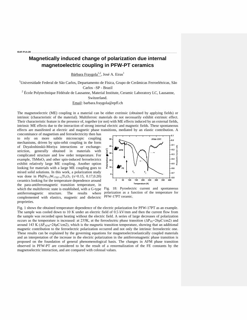
ISAF-P1A-28 ___________________________________________________________________________________________________________________
Magnetically induced change of polarization due internal
magnetoelectric coupling in PFW-PT ceramics
Bárbara Fraygola1,2
, José A. Eiras1
1Universidade Federal de São Carlos, Departamento de Física, Grupo de Cerâmicas Ferroelétricas, São
Carlos –SP - Brazil
2 École Polytechnique Fédérale de Lausanne, Material Institute, Ceramic Laboratory LC, Lausanne,
Switzerland.
Email: [email protected]
The magnetoelectric (ME) coupling in a material can be either extrinsic (obtained by applying fields) or
intrinsic (characteristic of the material). Multiferroic materials do not necessarily exhibit extrinsic effect.
Their characteristic feature is the presence of, together (or not) with ME effects induced by an external fields,
intrinsic ME effects due to the interaction of strong internal electric and magnetic fields. These spontaneous
effects are manifested at electric and magnetic phase transitions, mediated by an elastic contribution. A
concomitance of magnetism and ferroelectricity then has
to rely on more subtle microscopic coupling
mechanisms, driven by spin-orbit coupling in the form
of Dzyaloshinskii-Moriya interactions or exchange-
striction, generally obtained in materials with
complicated structure and low order temperature. For
example, TbMnO3 and other spin-induced ferroelectrics
exhibit relatively large ME coupling. Another option
looking for materials with a large ME coupling goes to
mixed solid solutions. In this work, a polarization study
was done in Pb(Fe2/3W1/3)(1-x)TixO3 (x=0.15, 0.17,0.20)
ceramics looking for the temperature dependence around
the para-antiferromagnetic transition temperature, in
which the multiferroic state is established, with a G-type
antiferromagnetic structure. The results where
complemented with elastics, magnetic and dielectric
proprieties.
Fig. 1 shows the obtained temperature dependence of the electric polarization for PFW-17PT as an example.
The sample was cooled down to 10 K under an electric field of 0.5 kV/mm and then the current flow from
the sample was recorded upon heating without the electric field. A series of large decreases of polarization
occurs as the temperature is increased: at 235K, at the ferroelectric phase transition (ΔPFE=26μC/cm2) and
around 143 K (ΔPAFM=24μC/cm2), which is the magnetic transition temperature, showing that an additional
magnetic contribution to the ferroelectric polarization occurred and not only the intrinsic ferroelectric one.
These results can be explained by the governing equations for magnetoelectroelastically coupled materials
and an interpretation of the increase in the electric polarization in the antiferromagnetic phase transition is
proposed on the foundation of general phenomenological basis. The changes in AFM phase transition
observed in PFW-PT are considered to be the result of a renormalization of the FE constants by the
magnetoelectric interaction, and are compared with colossal values.
Fig. 18: Pyroelectric current and spontaneous
polarization as a function of the temperature for
PFW-17PT ceramic.
0 50 100 150 200 250 300 350 400
0
10
20
30
40
50
Pir
oele
ctr
ic C
urr
en
t (
nA
)
Po
lari
za
tio
n (C
/cm
2)
Temperature (K)
-0.8
-0.7
-0.6
-0.5
-0.4
-0.3
-0.2
-0.1
0.0
0.1
PAFM
PFW-17PT
PFE
TC
TN
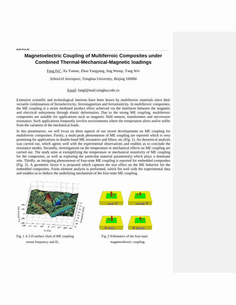
ISAF-P1A-30 ___________________________________________________________________________________________________________________
Magnetoelectric Coupling of Multiferroic Composites under
Combined Thermal-Mechanical-Magnetic loadings
Fang Fei1, Xu Yantao, Zhou Yangyang, Jing Wenqi, Yang Wei
School of Aerospace, Tsinghua University, Beijing 100084
Email: [email protected]
Extensive scientific and technological interests have been drawn by multiferroic materials since their
versatile combinations of ferroelectricity, ferromagnetism and ferroelasticity. In multiferroic composites,
the ME coupling is a strain mediated product effect achieved via the interfaces between the magnetic
and electrical subsystems through elastic deformation. Due to the strong ME coupling, multiferroic
composites are suitable for applications such as magnetic field sensors, transformers and microwave
resonators. Such applications frequently involve environments where the temperature alters and/or suffer
from the variation of the mechanical loads.
In this presentation, we will focus on three aspects of our recent developments on ME coupling for
multiferroic composites. Firstly, a multi-peak phenomenon of ME coupling are reported which is very
promising for applications in double-band ME resonators and filters, etc (Fig. 1). An theoretical analysis
was carried out, which agrees well with the experimental observations and enables us to conclude the
resonance modes. Secondly, investigations on the temperature or mechanical effects on ME coupling are
carried out. The study aims at exemplifying the temperature or mechanical sensitivity of ME coupling
for the composites, as well as exploring the particular material parameter(s) which plays a dominant
role. Thirdly, an intriguing phenomenon of four-state ME coupling is reported for embedded composites
(Fig. 2). A geometric factor k is proposed which captures the size effect on the ME behavior for the
embedded composites. Finite element analysis is performed, which fits well with the experimental data
and enables us to deduce the underlying mechanism of the four-state ME coupling.
Fre
quency (
kH
z)
M
E(m
V/c
mO
e)
Hs (Oe)
H
P
H
H H
P
PP
Fig. 1 A 3-D surface chart of ME coupling Fig. 2 Schematics of the four-state
versus frequency and Hs. magnetoelectric coupling.
ISAF-P1A-31 ___________________________________________________________________________________________________________________
Phase transitions of high insulating rhombohedral Bi1-
xLaxFe1-yTiyO3 multiferroic ceramics
Jian Yu and Linlin Zhang
Functional Materials Research Laboratory, Tongji University, Shanghai 200092, China
Email: [email protected]
BiFeO3 is the only known high temperature single-phased multiferroic material, which exhibits
coexistence of ferroelectric and antiferromagnetic ordering below Néel temperature of 370oC. Owing to
thermodynamic instability of BiFeO3 compound, it is very difficult to prepare phase pure samples, often
accompanying with impurities of Bi25FeO39 and Bi2Fe4O9. Meanwhile, synthesization of high insulating
BiFeO3 ceramics is a major challenge for material scientists.
In this report, Bi1-xLaxFe1-yTiyO3 multiferroic ceramics with 0.02 ≤ x ≤ 0.12 and 0.01 ≤ y ≤ 0.08 were
prepared with refined electroceramic processing of traditional solid state reaction method. It was found
experimentally that La/Ti-codoping stabilizes rhombohedral BiFeO3 through forming ternary solid
solution. Then the electrical properties of robust insulating with resistivity of ~1011
m under 90 kV/cm
electric field and low dielectric loss below 0.03 over the frequency range of 20 - 1M Hz were obtained
for all composition studied here. Their robust insulating property was also able to be demonstrated by
poling experiments, for example, the Bi0.98La0.02 Fe0.99Ti0.01O3 ceramics bore more than 5kV DC electric
field at 120oC and then exhibited piezoelectric constant of d33 = 0.6 pC/N. The mechanisms for high
insulating and low dielectric loss were also experimentally investigated and discussed relating to defect
and thermodynamic stability of BiFeO3.
For these rhombohedral Bi1-xLaxFe1-yTiyO3 multiferroic ceramics, differential thermal analysis,
temperature-dependent X-ray diffraction and magnetization measurements probe four structural phase
transitions, e.g. TH = 305oC, TN = 365
oC, TC = 810
oC and TS = 830
oC observed in the
Bi0.98La0.02Fe0.99Ti0.01O3, which are reasonably attributed to antiferromagnetic-helimagnetic,
helimagnetic-paramagnetic, ferroelectric-paraelectric and rhombohedral-cubic lattice structural phase
transition, respectively. With increasing x and y in our experiments, TH and TN changes little but TC and
TS decrease gradually. The change of magnetic phase transition from second-order to first-order and
emergence of helimagnetic ordering phase was attributed to Ti3+
d1 disordered distribution in the -Fe
3+
d5-O-Fe
3+ d
5-O-Fe
3+ d
5-O- chains.
The rhombohedral Bi1-xLaxFe1-yTiyO3 multiferroic ceramics with robust insulating and low dielectric
loss may be able to find possible applications as microwave dielectrics, different from those normal
diamagnetic dielectrics.
ISAF-P1A-32 ___________________________________________________________________________________________________________________
Mixtures of the ferroelectric liquid crystal and magnetic
nanoparticles: New Soft Magnetoelectrics
Brigita Rožič1,2
, Marko Jagodič3,4
, Sašo Gyergyek1, George Cordoyiannis
1,2,5, Mihael Drofenik
1, Zvonko
Jagličić3,6
, Samo Kralj7, Vassilios Tzitzios
8 and Zdravko Kutnjak
1,2,9
1Jozef Stefan Institute, Jamova cesta 39, 1000 Ljubljana, Slovenia
2Centre of Excellence Namaste, Jamova cesta 39, 1000 Ljubljana, Slovenia
3Institute of Mathematics, Physics and Mechanics, Jadranska 19, 1000 Ljubljana, Slovenia
4EN-FIST Centre of Excellence Namaste, Dunajska 156, 1000 Ljubljana, Slovenia
5Department of Physics, University of Athens, 15784 Athens, Greece
6Faculty of Civil and Geodetic Engineering, Jamova cesta 2, 1000 Ljubljana
7Faculty of Natural Science and Mathematics, Koroška cesta 160, 2000 Maribor, Slovenia
8National Centre for Scientific Research Demokritos, Aghia Paraskevi 15310, Greece
9Jozef Stefan International Postgraduate School, 1000 Ljubljana, Slovenia
Email: [email protected]
Magnetoelectrics have recently attracted significant attention due to their properties and potential for
various applications69
. So far the main focus remains on solid magnetoelectrics, but in our case we
focused on the magnetoelectric effect in a soft material based on mixtures of a ferroelectric liquid crystal
(FLC) and magnetic nanoparticles (MNPs).
In this work we report the theoretical estimation and experimental observation of the magnetoelectric
effect in similar systems of two different FLCs, i.e., SCE9 and Felix 015/100, and two different
ferromagnetic NPs, i.e., maghemite and magnetite magnetic NPs70,71,72
. NPs were weakly anisotropic
with an average size of 20 nm and coated with an oleic acid to avoid instability of the suspension in the
toluene. The high resolution calorimetry, dielectric spectroscopy and magnetic susceptibility
measurements were performed in the vicinity of the ferroelectric phase transition. Similar disordering
effects on the ferroelectric phase transition were found as in the case of the aerosils73
and the impact of
the MNPs on the dielectric response was observed. Measurements of the impact of the electric field on
the magnetic susceptibility via SQUID-based magnetometer confirmed the indirect coupling between
the NP’s magnetic moments and LC’s electric polarization.
Obtained experimental results are in good agreement with the theoretical predictions and they provide a
strong support for the generally expected behavior in such mixtures. This enhances the chance to
engineer the soft composite magnetoelectrics.
69
W. Erenstein et al., “Multiferroic and magnetoelectric materials”, Nature, vol. 442, 05023, 2006. 70
B. Rožič et al., “Orientational order-magnetization coupling in mixtures of magnetic nanoparticles and the ferroelectric
liquid crystal”, Ferroelectrics, vol. 410, p. 37-41, 2011. 71
B. Rožič et al., “Multiferroic behavior in mixtures of the ferroelectric liquid crystal and magnetic nanoparticles”, Mol.
Cryst. Liq. Cryst., vol. 545, p. 99-104, 2011. 72
B. Rožič et al., “Mixtures of magnetic nanoparticles and ferroelectric liquid crystal: New soft magnetoelectrics”,
Ferroelectrics, vol. 431, p. 150-153, 2012. 73
G. Cordoyiannis et al., “Pretransitional effects near the smectic A-smectic C* phase transition of hydrophilic and
hydrophobic aerosil networks dispersed in ferroelectric liquid crystals”, Phys. Rev. E, vol. 75, 021702, 2007.
ISAF-P1A-33 ___________________________________________________________________________________________________________________
Epitaxial (Sr1-xBax)MnO3 thin films: towards strain-induced
ferroelectricity
L. Maurel1,2
, J. A. Pardo1,3,*
, M. Algueró4, C. Becher
5, E. Langenberg
1, J. Blasco
2,6, C. Magén
1,2, P.
Ramos7, R. Jiménez
4, J. Ricote
4, P. Štrichovanec
1, I. Lucas
2,6, L. Morellón
1,2, M. Fiebig
5, M. R. Ibarra
1,2,
P. A. Algarabel2,6
1INA, University of Zaragoza, Spain.
2Condensed Matter Physics Dept., University of Zaragoza, Spain.
3Materials Science Dept., University of Zaragoza, Spain.
4ICMM-CSIC, Cantoblanco, Spain.
5Materials
Dept., ETH, Switzerland. 6ICMA-CSIC, Zaragoza, Spain.
7Dpto. Electrónica, UAH, Alcalá de Henares,
Spain
(*) email: [email protected]
Recent theoretical predictions and experimental results suggest that paraelectric SrMnO3 with the ABO3
perovskite structure could become ferroelectric upon artificial expansion of the unit cell, either by
epitaxial strain1 or partial substitution of Ba for Sr (ref.
2). This would give rise to a new class of
multiferroic pervoksites where ferroelectricity would be driven by off-centring of the magnetic cation
Mn4+
.
Here we have investigated the effect of both Ba doping and epitaxial strain on the structure and electric
properties of SrMnO3 thin films. Pulsed laser deposition with in situ RHEED monitoring was used to
grow strained (Sr1-xBax)MnO3, 0≤x≤0.5 (SBMO) thin films on (001)-oriented perovskite substrates, with
strain ranging from -1% (compressive) to +3% (tensile). X-ray diffraction shows that, under appropriate
deposition conditions, the perovskite pseudocubic phase is stabilized over the hexagonal phase, despite
the latter being favored with increasing Ba content. Optimized films show fully coherent cube-on-cube
epitaxial growth and are chemically homogeneous and defect-free, as determined by scanning
transmission electron microscopy and electron energy loss spectroscopy.
Nonlinear optics measurements reveal that some of our SBMO films emit optical second harmonic
generation signal, pointing to spatial inversion symmetry being broken (necessary condition for
ferroelectricity). Electric measurements and piezoresponse force microscopy were used to investigate
the ferroelectric properties of epitaxially strained SBMO films.
__________________________________
1 J. H. Lee and K. M. Rabe, Phys. Rev. Lett. 104, 207204 (2010)
2 H. Sakai et al., Phys. Rev. Lett. 107, 137601 (2011)
ISAF-P1A-34 ___________________________________________________________________________________________________________________
The Magnetoelectric Coupling in a Self-Assembled Epitaxial
Nano-composite Driven by Chemical Interaction
Wen-I Liang1, Yuanming Liu
2, Wei-Cheng Wang
3,Heng-Jui Liu
1, Sheng-Chieh Laio
4, Hong-Ji Lin
3,
Chih-Huang Lai4, Elke Arenholz
5, Jaingyu Li
2, Ying-Hao Chu
1
1Department of Materials Science and Engineering, National Chiao Tung University, HsinChu, 30010,
Taiwan 2Department of Mechanical Engineering, University of Washington, Seattle, WA 98195, USA
3National Synchrotron Radiation Research Center, Hsinchu 30076, Taiwan
4Department of Materials Science and Engineering, National Tsing Hua University, Hsinchu 30013,
Taiwan 5Advanced Light Source, Berkeley, CA 94720, USA
Email: [email protected]
Complex oxide heterostructures have triggered a plethora of studies with novel phenomena in
condensed matter physics because it provides the possibility to integrate dissimilar oxide with diverse
functionalities. Among them, self-assembled vertical nano-composite, as one approach to build
heterostrucutre, has enlarged the playground of complex oxide heterostructure due to structural, physical
and chemical interactions between dissimilar oxides. From the previous studies, the structural and
physical interactions are demonstrated comprehensively; however, the information of chemical
interaction, or atomic diffusion, which is more or less inevitable in two-phase system, is still missing so
far. In this study, it is designed the chemical-interaction-induced magnetoelectric coupling effect exhibits
in two antiferromagnetic materials: BiFeO3 and LiMn2O4 vertical nano-composite.
The self-assembled (BiFeO3)x:(LiMn2O4)1-x vertical heterostructure with different composition ratio
were grown by pulse laser deposition. Via the scrutiny of scanning electron microscope, X-ray
diffraction, nano Auger and high resolution transmission electron microscope, a fundamental view
between the inter-diffusion and the composition ratio is visualized. Based on this chemical interaction,
we have found the both ferroelectricity and ferromagnetism coexist in the (BiFeO3)0.75:(LiMn2O4)0.25
nano-heterostructure. Furthermore, in order to understand this behavior, a concrete connection between
chemical diffusion and the induced magnetic moment is proposed when we conduct soft x-ray circular
dichroism to investigate the local environment of transition metals. The last part of this study shows the
strong magnetoelectric coupling effect between these two chemical changed phases. Thus, in this study,
we have manipulated successively the chemical interaction between dissimilar oxides heterostructure to
demonstrate the new-emerged physical properties and its coupling effect, which would be a key study to
extend the practical value in vertical nanoheterostructure.
ISAF-P1A-35 ___________________________________________________________________________________________________________________
Effect of composition on functional properties of ferroelectric-ferrite composite systems
Cristina Elena Ciomaga
1, Mihai Valentin Pop
1, Leontin Padurariu
1, Mirela Airimioaei
2, Carmen Galassi
3
and Liliana Mitoseriu1
1Faculty of Physics, “Al. I. Cuza” University of Iasi 700506, Romania
2Faculty of Chemistry, “Al. I. Cuza” University of Iasi 700506, Romania
3CNR -ISTEC, Via Granarolo no. 64, I-48018 Faenza, Italy
E-mail: [email protected]
The ferroelectric, dielectric and magnetic properties related to the microstructures in the xNiFe2O4-(1-
x)Pb0.988(Zr0.52Ti0.48)0.976Nb0.024O3 (xNF-(1-x)PZTNb) magneto-electric composites with x= 2, 5, 10, 20,
30, 40, 50, 60, 70 and 100 wt% are investigated. The di-phase ceramics prepared in situ by sol-gel
method present homogeneous microstructures, higher density and a better mixing of the two phases.
The temperature dependence of dielectric properties showed a sharp ferroelectric to paraelectric phase
transition peak at around 360°C for low NF concentrations and a diffuse phase transition at around
330°C for high amounts of ferrite in the composites. Thus, the addition of NF phase induces a
microscopic heterogeneity in composites and a distribution of different localized Curie points. From
frequency dependence of the complex dielectric permittivity it was observed a dispersive behavior, due
to Maxwell-Wagner effect. The higher degree addition of magnetic phase contributes to the interfacial
polarization, causing a significant increase of the real part of permittivity for frequencies below 1 kHz.
The ferroelectric properties reveal that with increasing the NF concentration in the composites it was
obtained flattened P-E loops with smaller values of the remnant polarization. In contrast, the magnetic
properties improve with addition of ferrite phase. However the coercitive field (Hc) for all the composite
samples is larger than that of pure NiFe2O4 phase.
For describing the dependence of the polarization on the applied electric field, a combined model based
on Classical Preisach Model (CPM) and Finite Element Method (FEM) was developed and compared
with the experimental data.
Acknowledgements: These works were financial supported by CNCSIS-UEFISCSU, projects number
PN II-RU TE code 187/2010 and PN-II-ID-PCE-2011-3-0745.
ISAF-P1A-36 ___________________________________________________________________________________________________________________
Influence of substrate–film interface engineering on the multiferroic BiFeO3
Alim Solmaz1, Mark Huijben
1, Beatriz Noheda
2, Guus Rijnders
1
1Mesa+ Institute for Nanotechnology , University of Twente, Enschede, The Netherlands
2Zernike Institute for Advanced Materials, University of Groningen, Groningen, The Netherlands
Email: [email protected]
Multiferroics, such as BiFeO3, which simultaneously exhibit multiple order parameters such as
antiferromagnetism and ferroelectricity, enable the development of novel magnetoelectric devices by
utilizing the intrinsic magnetoelectric coupling in which one can control the electric polarization by
applied magnetic fields or the magnetism by applied electric fields. This could lead to new applications
in magnetic data storage, spintronics, and high-frequency magnetic devices, which do not require large
currents and magnetic fields for operation.
In bulk, BiFeO3 is a rhombohedrally distorted perovskite crystal where the ferroelectricity arises due to
the displacement of Bi ions with respect to FeO6 octahedra. This results in an electrical polarization that
lies along the <111>pc directions and, thereby, to formation of three types of domain walls i.e. 71˚, 109˚
and 180˚, each of which show distinctive properties such as conductivity and magnetism. In addition to
that, the antiferromagnetic properties of BiFeO3 are exploited in order to create an exchange bias with a
ferromagnetic layer such that two coupling effects can be used to manipulate the ferromagnetic state by
electric field74
. Additionally, it has been shown that a ferromagnetic state can be induced at the interface
between BiFeO3 and La0.7Sr0.3MnO3 thin films75
. Thus it is important to have atomic level control of the
growth of BiFeO3 thin films in order to obtain specific properties at domain walls and interfaces.
In our work, we focus on the heteroepitaxial growth of BiFeO3 single crystal thin films on SrTiO3
substrates by pulsed laser deposition. We demonstrate that the initial BiFeO3 growth is very sensitive to
the terminating layer of the substrate. Singly TiO2-terminated substrates can be switched to SrO
termination by interval deposition with the assistance of Reflective High Energy Electron Diffraction
(RHEED) technique. BiFeO3 thin films grown on SrO and TiO2 singly-terminated substrates show
different morphologies as well as different ferroelectric domains. This indicates that the sticking of
bismuth oxide species on TiO2-terminated surfaces is different than that of iron oxide on SrO terminated
surfaces. This determines the interface quality between the BiFeO3 thin film and the substrate. Keeping
in mind that the interfaces become more influential as the film gets thinner, we emphasize the
importance of interface engineering for highly controlled multiferroic devices. We claim that, in BiFeO3
thin film growth, the atomic terminating layer of the substrate should be taken into account as well, next
to other factors that are known to influence the ferroelectric domain formation, such as screening
charges, lattice mismatch or substrate miscut.
74
Chu Y. et al., Electric-field control of local ferromagnetism using a magnetoelectric multiferroic , Nat. Mater., 7, 478-
(2008). 75
Yu P. et al, Interface Ferromagnetism and Orbital Reconstruction in BiFeO3-LaSrMnO Heterostructures, PRL 105, 27201
(2010).
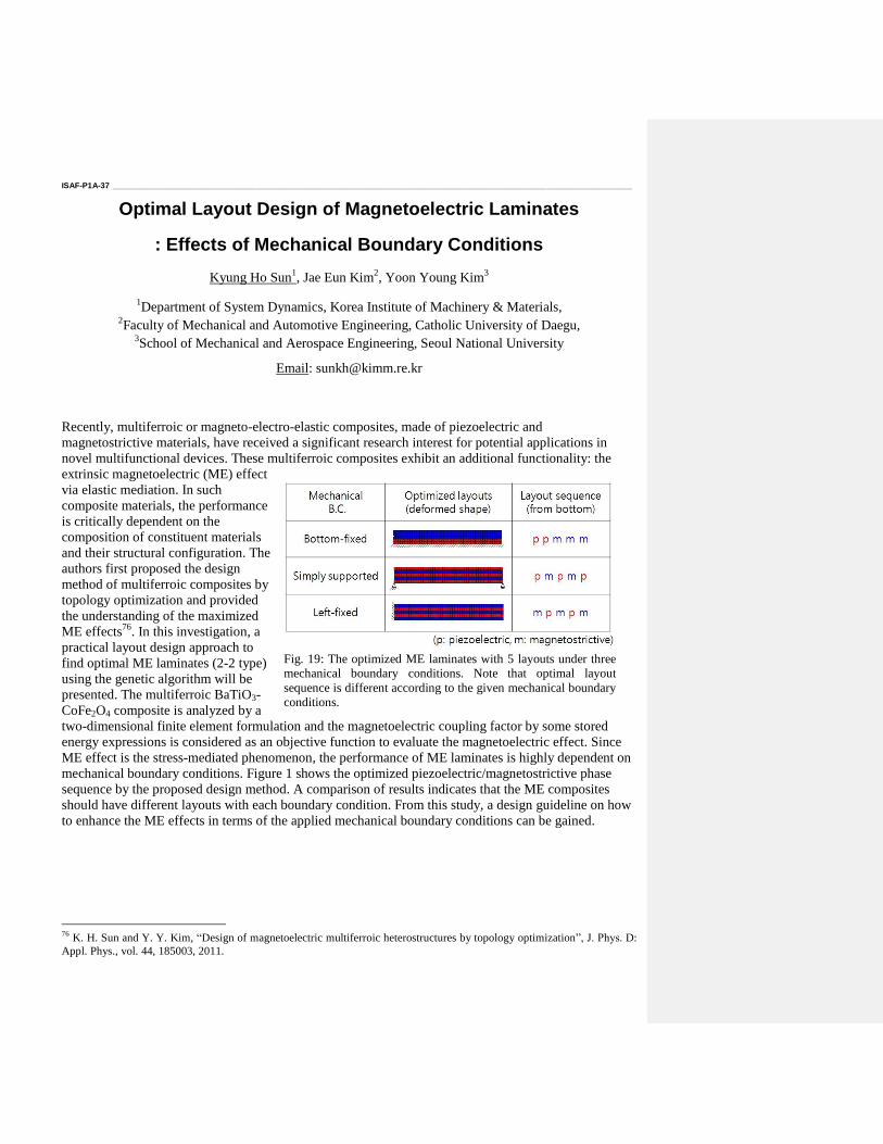
ISAF-P1A-37 ___________________________________________________________________________________________________________________
Optimal Layout Design of Magnetoelectric Laminates
: Effects of Mechanical Boundary Conditions
Kyung Ho Sun1, Jae Eun Kim
2, Yoon Young Kim
3
1Department of System Dynamics, Korea Institute of Machinery & Materials,
2Faculty of Mechanical and Automotive Engineering, Catholic University of Daegu,
3School of Mechanical and Aerospace Engineering, Seoul National University
Email: [email protected]
Recently, multiferroic or magneto-electro-elastic composites, made of piezoelectric and
magnetostrictive materials, have received a significant research interest for potential applications in
novel multifunctional devices. These multiferroic composites exhibit an additional functionality: the
extrinsic magnetoelectric (ME) effect
via elastic mediation. In such
composite materials, the performance
is critically dependent on the
composition of constituent materials
and their structural configuration. The
authors first proposed the design
method of multiferroic composites by
topology optimization and provided
the understanding of the maximized
ME effects76
. In this investigation, a
practical layout design approach to
find optimal ME laminates (2-2 type)
using the genetic algorithm will be
presented. The multiferroic BaTiO3-
CoFe2O4 composite is analyzed by a
two-dimensional finite element formulation and the magnetoelectric coupling factor by some stored
energy expressions is considered as an objective function to evaluate the magnetoelectric effect. Since
ME effect is the stress-mediated phenomenon, the performance of ME laminates is highly dependent on
mechanical boundary conditions. Figure 1 shows the optimized piezoelectric/magnetostrictive phase
sequence by the proposed design method. A comparison of results indicates that the ME composites
should have different layouts with each boundary condition. From this study, a design guideline on how
to enhance the ME effects in terms of the applied mechanical boundary conditions can be gained.
76
K. H. Sun and Y. Y. Kim, “Design of magnetoelectric multiferroic heterostructures by topology optimization”, J. Phys. D:
Appl. Phys., vol. 44, 185003, 2011.
Fig. 19: The optimized ME laminates with 5 layouts under three
mechanical boundary conditions. Note that optimal layout
sequence is different according to the given mechanical boundary
conditions.
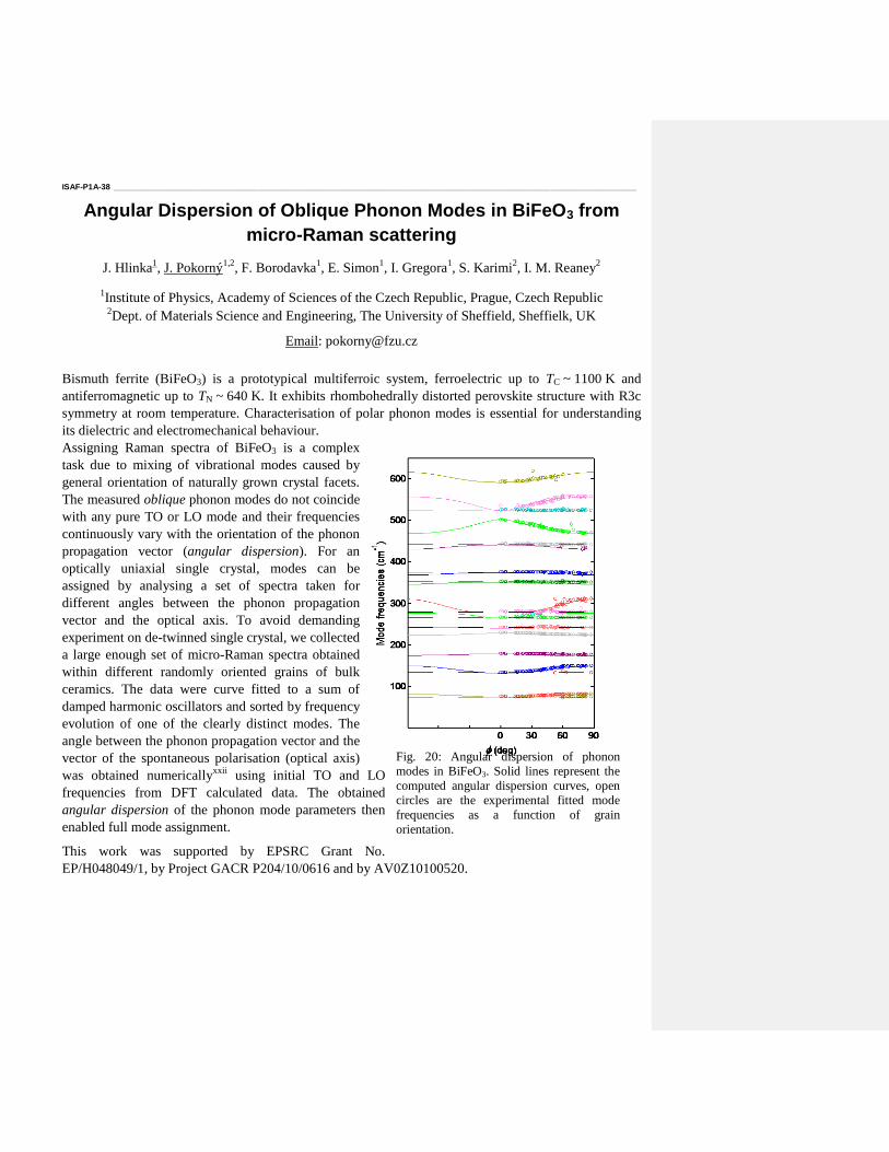
ISAF-P1A-38 ___________________________________________________________________________________________________________________
Angular Dispersion of Oblique Phonon Modes in BiFeO3 from
micro-Raman scattering
J. Hlinka1, J. Pokorný
1,2, F. Borodavka
1, E. Simon
1, I. Gregora
1, S. Karimi
2, I. M. Reaney
2
1Institute of Physics, Academy of Sciences of the Czech Republic, Prague, Czech Republic 2Dept. of Materials Science and Engineering, The University of Sheffield, Sheffielk, UK
Email: [email protected]
Bismuth ferrite (BiFeO3) is a prototypical multiferroic system, ferroelectric up to TC ~ 1100 K and
antiferromagnetic up to TN ~ 640 K. It exhibits rhombohedrally distorted perovskite structure with R3c
symmetry at room temperature. Characterisation of polar phonon modes is essential for understanding
its dielectric and electromechanical behaviour.
Assigning Raman spectra of BiFeO3 is a complex
task due to mixing of vibrational modes caused by
general orientation of naturally grown crystal facets.
The measured oblique phonon modes do not coincide
with any pure TO or LO mode and their frequencies
continuously vary with the orientation of the phonon
propagation vector (angular dispersion). For an
optically uniaxial single crystal, modes can be
assigned by analysing a set of spectra taken for
different angles between the phonon propagation
vector and the optical axis. To avoid demanding
experiment on de-twinned single crystal, we collected
a large enough set of micro-Raman spectra obtained
within different randomly oriented grains of bulk
ceramics. The data were curve fitted to a sum of
damped harmonic oscillators and sorted by frequency
evolution of one of the clearly distinct modes. The
angle between the phonon propagation vector and the
vector of the spontaneous polarisation (optical axis)
was obtained numericallyxxii
using initial TO and LO
frequencies from DFT calculated data. The obtained
angular dispersion of the phonon mode parameters then
enabled full mode assignment.
This work was supported by EPSRC Grant No.
EP/H048049/1, by Project GACR P204/10/0616 and by AV0Z10100520.
Fig. 20: Angular dispersion of phonon
modes in BiFeO3. Solid lines represent the
computed angular dispersion curves, open
circles are the experimental fitted mode
frequencies as a function of grain
orientation.
ISAF-P1A-39 ___________________________________________________________________________________________________________________
Structural Phase Transitions in Bi1-xCaxFeO3 Multiferroics
V. A. Khomchenko1, I. O. Troyanchuk
2, D. M. Többens
3, V. Sikolenko
4, J. A. Paixão
1
1CEMDRX/Department of Physics, University of Coimbra, Coimbra, Portugal
2SSPA “Scientific-Practical Materials Research Centre of NAS of Belarus”, Minsk, Belarus
3Helmholtz-Zentrum-Berlin for Materials and Energy, Berlin, Germany
4Laboratory for Neutron Scattering, Paul Scherrer Institute, Villigen, Switzerland
Email: [email protected]
BiFeO3 perovskite remains one of the most popular objects of condensed matter research. Indeed, the
coexistence of spin and electric dipole ordering observed in this material in a broad temperature range
and giving rise to the promissing cross-coupling effects is interesting from the viewpoint of both
fundamental and applied physics. BiFeO3 crystallizes in a rhombohedral R3c structure permitting the
polar ionic displacements along the <111>c direction of the parent cubic perovskite cell. To be suitable
for applications, the polarization should be coupled to the net magnetization, which is, however, locked
in the cycloidal modulation superimposed on the G-type antiferromagnetic (with a weak ferromagnetic
component) structure. One of the ways allowing the modulation to be suppressed is a chemical
substitution.
In present work, the neutron powder diffraction and magnetization measurements of the Bi1-xCaxFeO3
(0.05≤x≤0.14) compounds belonging to the intermediate concentration range separating the polar
antiferromagnetic (x~0) and nonpolar antiferromagnetic (x~0.2) phases have been carried out. It has
been shown that Ca substitution induces appearance of weak ferromagnetism in the initial ferroelectric
R3c phase, but modifies the picture of polar displacements, so the average PbZrO3-like antiferroelectric
structure (S.G. Pbam) is stabilized at x=0.11. Further increase of the Ca content leads to the
transformation of the antipolar ionic shifts to give rise to the Pbam→Imma transition near x=0.14. A
structural study performed for the x=0.05 compound at high temperature reveals the heating-induced
R3c→Pnma phase transition. Analysis of the compositional dependence of the spontaneous
magnetization and polarization in the R3c phase shows that Ca2+
substitution ensures a balanced
influence on the magnetic and ferroelectric subsystems of BiFeO3 allowing its multiferroic behavior to
be improved.
This work is supported by funds from FEDER (Programa Operacional Factores de Competitividade
COMPETE) and from FCT-Fundação para a Ciência e a Tecnologia under the project PEst-
C/FIS/UI0036/2011.
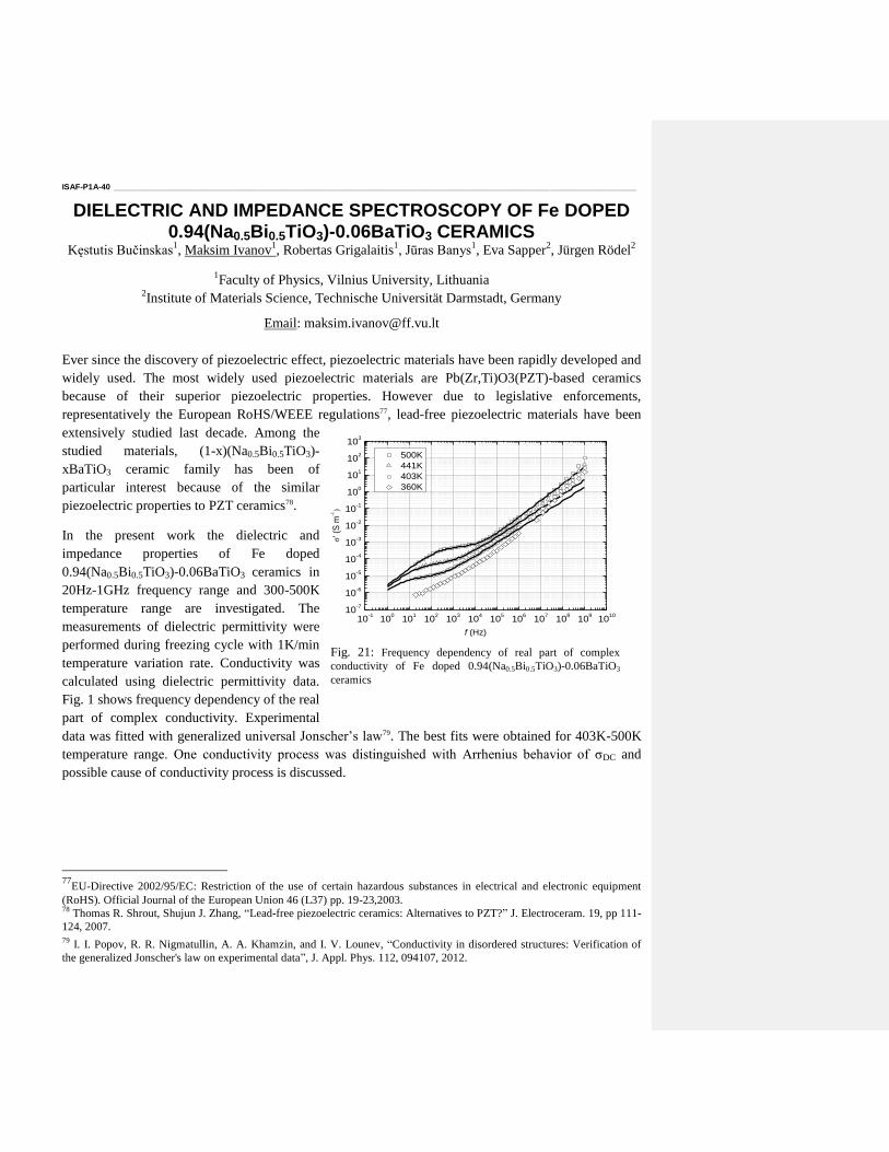
ISAF-P1A-40 ___________________________________________________________________________________________________________________
DIELECTRIC AND IMPEDANCE SPECTROSCOPY OF Fe DOPED 0.94(Na0.5Bi0.5TiO3)-0.06BaTiO3 CERAMICS
Kęstutis Bučinskas1, Maksim Ivanov
1, Robertas Grigalaitis
1, Jūras Banys
1, Eva Sapper
2, Jürgen Rödel
2
1Faculty of Physics, Vilnius University, Lithuania
2Institute of Materials Science, Technische Universität Darmstadt, Germany
Email: [email protected]
Ever since the discovery of piezoelectric effect, piezoelectric materials have been rapidly developed and
widely used. The most widely used piezoelectric materials are Pb(Zr,Ti)O3(PZT)-based ceramics
because of their superior piezoelectric properties. However due to legislative enforcements,
representatively the European RoHS/WEEE regulations77, lead-free piezoelectric materials have been
extensively studied last decade. Among the
studied materials, (1-x)(Na0.5Bi0.5TiO3)-
xBaTiO3 ceramic family has been of
particular interest because of the similar
piezoelectric properties to PZT ceramics78.
In the present work the dielectric and
impedance properties of Fe doped
0.94(Na0.5Bi0.5TiO3)-0.06BaTiO3 ceramics in
20Hz-1GHz frequency range and 300-500K
temperature range are investigated. The
measurements of dielectric permittivity were
performed during freezing cycle with 1K/min
temperature variation rate. Conductivity was
calculated using dielectric permittivity data.
Fig. 1 shows frequency dependency of the real
part of complex conductivity. Experimental
data was fitted with generalized universal Jonscher’s law79. The best fits were obtained for 403K-500K
temperature range. One conductivity process was distinguished with Arrhenius behavior of σDC and
possible cause of conductivity process is discussed.
77
EU-Directive 2002/95/EC: Restriction of the use of certain hazardous substances in electrical and electronic equipment
(RoHS). Official Journal of the European Union 46 (L37) pp. 19-23,2003. 78
Thomas R. Shrout, Shujun J. Zhang, “Lead-free piezoelectric ceramics: Alternatives to PZT?” J. Electroceram. 19, pp 111-
124, 2007. 79
I. I. Popov, R. R. Nigmatullin, A. A. Khamzin, and I. V. Lounev, “Conductivity in disordered structures: Verification of
the generalized Jonscher's law on experimental data”, J. Appl. Phys. 112, 094107, 2012.
10-1
100
101
102
103
104
105
106
107
108
109
1010
10-7
10-6
10-5
10-4
10-3
10-2
10-1
100
101
102
103
500K
441K
403K
360K
' (
S m
f (Hz)
Fig. 21: Frequency dependency of real part of complex
conductivity of Fe doped 0.94(Na0.5Bi0.5TiO3)-0.06BaTiO3
ceramics
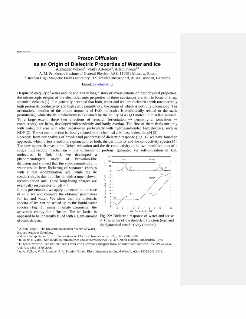
ISAF-P1A-41 ___________________________________________________________________________________________________________________
Proton Diffusion as an Origin of Dielectric Properties of Water and Ice
Alexander Volkov1, Vasily Artemov
1, Artem Pronin
1,2
1 A. M. Prokhorov Institute of General Physics, RAS, 119991 Moscow, Russia
2 Dresden High Magnetic Field Laboratory, HZ Dresden-Rossendorf, 01314 Dresden, Germany
Email: [email protected]
Despite of ubiquity of water and ice and a very long history of investigations of their physical properties,
the microscopic origins of the electrodynamic properties of these substances are still in focus of sharp
scientific debates [1]. It is generally accepted that both, water and ice, are dielectrics with unexpectedly
high proton dc conductivity and high static permittivity, the origin of which is not fully understood. The
orientational motion of the dipole moments of H2O molecules is traditionally related to the static
permittivity, while the dc conductivity is explained by the ability of a Н2О molecule to self-dissociate.
To a large extent, these two directions of research (orientation → permittivity, ionization →
conductivity) are being developed independently and hardy overlap. The first of them deals not only
with water, but also with other substances, particularly with hydrogen-bonded ferroelectrics, such as
KDP [2]. The second direction is closely related to the chemical acid-base index, the pH [3].
Recently, from our analysis of broad-band panoramas of dielectric response (Fig. 1), we have found an
approach, which offers a uniform explanation for both, the permittivity and the conductivity spectra [4].
The new approach reveals the Debye relaxation and the dc conductivity to be two manifestations of a
single microscopic mechanism – the diffusion of protons, generated via self-ionization of H2O
molecules. In Ref. [4], we developed a
phenomenological model of Brownian-like
diffusion and showed that the static permittivity of
water results from flickering of separated charges
with a fast recombination rate, while the dc
conductivity is due to diffusion with a much slower
recombination rate. These long-living charges are
eventually responsible for pH = 7.
In this presentation, we apply our model to the case
of solid ice and compare the obtained parameters
for ice and water. We show that the dielectric
spectra of ice can be scaled up to the liquid-water
spectra (Fig. 1), using a single parameter, the
activation energy for diffusion. The ice lattice is
appeared to be inherently filled with a giant amount
of ionic defects.
1 A. von Hippel, “The Dielectric Relaxation Spectra of Water,
Ice, and Aqueous Solutions,
and their Interpretation”, IEEE Transactions on Electrical Insulation, vol. 23, p. 801-816, 1988. 2 R. Blinc, B. Žekš, “Soft modes in ferroelectrics and antiferroelectrics“, p. 317, North-Holland, Amsterdam, 1974
3 D. Marx, “Proton Transfer 200 Years after von Grotthuss: Insights from Ab Initio Simulations“, ChemPhysChem,
Vol. 7, p. 1855-1870, 2006. 4
A. A. Volkov, V. G. Artemov, A. V. Pronin, “Proton Electrodynamics in Liquid Water“, arXiv:1302.5048, 2013.
Fig. 22: Dielectric response of water and ice at
0 °C in terms of the dielectric function (top) and
the dynamical conductivity (bottom).
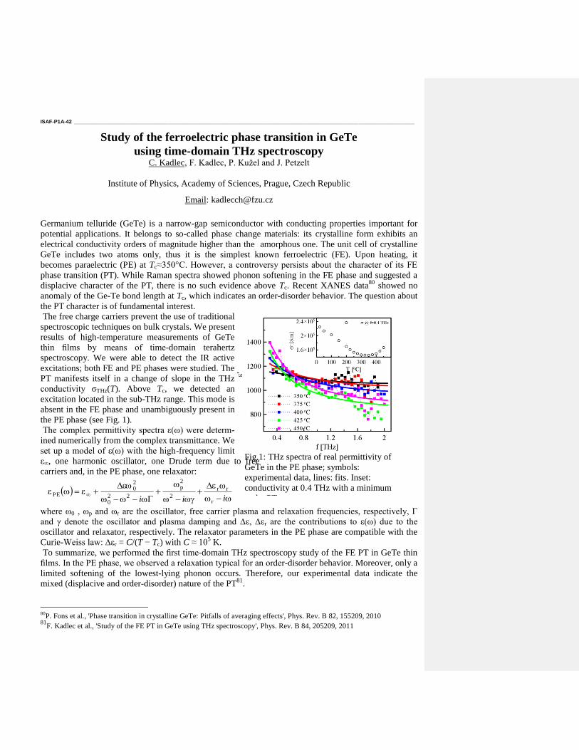
ISAF-P1A-42 ___________________________________________________________________________________________________________________
Study of the ferroelectric phase transition in GeTe
using time-domain THz spectroscopy C. Kadlec, F. Kadlec, P. Kužel and J. Petzelt
Institute of Physics, Academy of Sciences, Prague, Czech Republic
Email: [email protected]
Germanium telluride (GeTe) is a narrow-gap semiconductor with conducting properties important for
potential applications. It belongs to so-called phase change materials: its crystalline form exhibits an
electrical conductivity orders of magnitude higher than the amorphous one. The unit cell of crystalline
GeTe includes two atoms only, thus it is the simplest known ferroelectric (FE). Upon heating, it
becomes paraelectric (PE) at Tc≈350°C. However, a controversy persists about the character of its FE
phase transition (PT). While Raman spectra showed phonon softening in the FE phase and suggested a
displacive character of the PT, there is no such evidence above Tc. Recent XANES data80
showed no
anomaly of the Ge-Te bond length at Tc, which indicates an order-disorder behavior. The question about
the PT character is of fundamental interest.
The free charge carriers prevent the use of traditional
spectroscopic techniques on bulk crystals. We present
results of high-temperature measurements of GeTe
thin films by means of time-domain terahertz
spectroscopy. We were able to detect the IR active
excitations; both FE and PE phases were studied. The
PT manifests itself in a change of slope in the THz
conductivity σTHz(T). Above Tc, we detected an
excitation located in the sub-THz range. This mode is
absent in the FE phase and unambiguously present in
the PE phase (see Fig. 1).
The complex permittivity spectra ε(ω) were determ-
ined numerically from the complex transmittance. We
set up a model of ε(ω) with the high-frequency limit
ε∞, one harmonic oscillator, one Drude term due to free
carriers and, in the PE phase, one relaxator:
iii r
rr
2
2p
220
20
PE
where ω0 , ωp and ωr are the oscillator, free carrier plasma and relaxation frequencies, respectively, Γ
and γ denote the oscillator and plasma damping and ∆ε, ∆εr are the contributions to ε(ω) due to the
oscillator and relaxator, respectively. The relaxator parameters in the PE phase are compatible with the
Curie-Weiss law: ∆εr = C/(T − Tc) with C ≈ 105 K.
To summarize, we performed the first time-domain THz spectroscopy study of the FE PT in GeTe thin
films. In the PE phase, we observed a relaxation typical for an order-disorder behavior. Moreover, only a
limited softening of the lowest-lying phonon occurs. Therefore, our experimental data indicate the
mixed (displacive and order-disorder) nature of the PT81
.
80
P. Fons et al., 'Phase transition in crystalline GeTe: Pitfalls of averaging effects', Phys. Rev. B 82, 155209, 2010 81
F. Kadlec et al., 'Study of the FE PT in GeTe using THz spectroscopy', Phys. Rev. B 84, 205209, 2011
Fig.1: THz spectra of real permittivity of
GeTe in the PE phase; symbols:
experimental data, lines: fits. Inset:
conductivity at 0.4 THz with a minimum
at the PT.
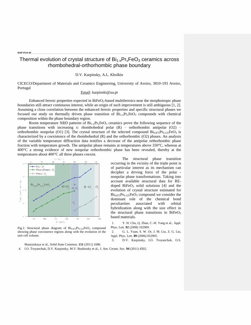
ISAF-P1A-43 ___________________________________________________________________________________________________________________
Thermal evolution of crystal structure of Bi1-xPrxFeO3 ceramics across rhombohedral-orthorhombic phase boundary
D.V. Karpinsky, A.L. Kholkin
CICECO/Department of Materials and Ceramics Engineering, University of Aveiro, 3810-193 Aveiro,
Portugal
Email: [email protected]
Enhanced ferroic properties expected in BiFeO3-based multiferroics near the morphotropic phase
boundaries still attract continuous interest, while an origin of such improvement is still ambiguous [1, 2].
Assuming a close correlation between the enhanced ferroic properties and specific structural phases we
focused our study on thermally driven phase transition of Bi1-xPrxFeO3 compounds with chemical
composition within the phase boundary region.
Room temperature XRD patterns of Bi1-xPrxFeO3 ceramics prove the following sequence of the
phase transitions with increasing x: rhombohedral polar (R) – orthorhombic antipolar (O2) –
orthorhombic nonpolar (O1) [3]. The crystal structure of the selected compound Bi0.875Pr0.125FeO3 is
characterized by a coexistence of the rhombohedral (R) and the orthorhombic (O2) phases. An analysis
of the variable temperature diffraction data testifies a decrease of the antipolar orthorhombic phase
fraction with temperature growth. The antipolar phase remains at temperatures above 350°C, whereas at
400°C a strong evidence of new nonpolar orthorhombic phase has been revealed, thereby at the
temperatures about 400°C all three phases coexist.
The structural phase transition
occurring in the vicinity of the triple point is
of particular interest as its mechanism can
decipher a driving force of the polar -
nonpolar phase transformations. Taking into
account available structural data for RE-
doped BiFeO3 solid solutions [4] and the
evolution of crystal structure estimated for
Bi0.875Pr0.125FeO3 compound we consider the
dominant role of the chemical bond
peculiarities associated with orbital
hybridization along with the size effect in
the structural phase transitions in BiFeO3
based materials.
1. Y. H. Chu, Q. Zhan, C.-H. Yang et al., Appl.
Phys. Lett. 92 (2008) 102909.
2. G. L. Yuan, S. W. Or, J. M. Liu, Z. G. Liu,
Appl. Phys. Lett. 89 (2006) 052905.
3. D.V. Karpinsky, I.O. Troyanchuk, O.S.
Mantytskaya et al., Solid State Commun. 151 (2011) 1686.
4. I.O. Troyanchuk, D.V. Karpinsky, M.V. Bushinsky et al., J. Am. Ceram. Soc. 94 (2011) 4502.
Fig.1: Structural phase diagram of Bi0.875Pr0.125FeO3 compound
showing phase coexistence regions along with the evolution of the
unit cell volume.
ISAF-P1A-44 ___________________________________________________________________________________________________________________
High temperature single-phased magnetic ferroelectrics: BiFeO3-
Bi(Zn1/2Ti1/2)O3-PbTiO3 ceramics
Linlin Zhang, Xianbo Hou, Jian Yu*
Functional Materials Research Laboratory, Tongji University, Shanghai, China
Email: [email protected] *[email protected]
Multiferroic materials have been attracting an increasingly fundamental and practical interest. Owing to
the lacking of high-temperature single-phased ferromagnetic-ferroelectric multiferroics with strong
linear magnetoelectric coupling effect, these materials have not been widely applied yet. Meanwhile,
synthesization of pure single-phased and high insulating material is a major challenge for material
scientists. Here, perovskite-structured BiFeO3-Bi(Zn1/2Ti1/2)O3-PbTiO3 solid solutions, fabricated with
conventional electroceramic processing and sintered at temperature around 890oC, were systematically
investigated. The authors reported on the dielectric, ferroelectric and magnetic properties of the ternary
solid solutions. It was found that high insulating and low dielectric loss ceramics are obtained for the (1-
2x)BiFeO3-xBi(Zn1/2Ti1/2)O3-xPbTiO3 ceramics (0.05 ≤ x ≤ 0.25). Pure rhombohedral phase of
0.7BiFeO3-0.14Bi(Zn1/2Ti1/2)O3-0.16PbTiO3 was obtained, with the dielectric loss below 0.04@1kHz,
which bore 4kV DC electric field at 100oC and exhibited piezoelectric constant of d33 = 0.5 pC/N. Two
ferroic phase transition temperatures of TN ~ 330 o
C and TC ~ 810 o
C were detected from DSC and DTA
measurements, respectively. The magnetic and electrical properties were also studied under different
heat treatments. Our researching is to design high temperature high performanced perovskite-structured
magnetic-ferroelectric multiferroic compounds.
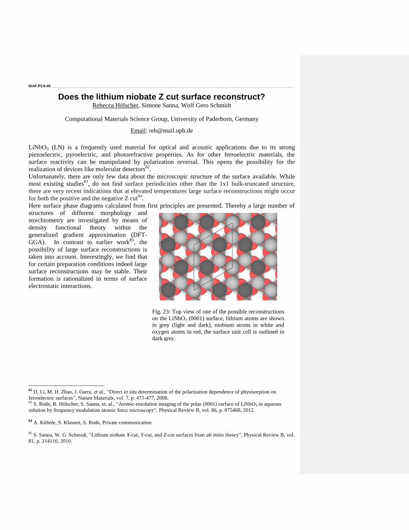
ISAF-P1A-45 ___________________________________________________________________________________________________________________
Does the lithium niobate Z cut surface reconstruct? Rebecca Hölscher, Simone Sanna, Wolf Gero Schmidt
Computational Materials Science Group, University of Paderborn, Germany
Email: [email protected]
LiNbO3 (LN) is a frequently used material for optical and acoustic applications due to its strong
piezoelectric, pyroelectric, and photorefractive properties. As for other ferroelectric materials, the
surface reactivity can be manipulated by polarization reversal. This opens the possibility for the
realization of devices like molecular detectors82
.
Unfortunately, there are only few data about the microscopic structure of the surface available. While
most existing studies83
, do not find surface periodicities other than the 1x1 bulk-truncated structure,
there are very recent indications that at elevated temperatures large surface reconstructions might occur
for both the positive and the negative Z cut84
.
Here surface phase diagrams calculated from first principles are presented. Thereby a large number of
structures of different morphology and
stoichiometry are investigated by means of
density functional theory within the
generalized gradient approximation (DFT-
GGA). In contrast to earlier work85
, the
possibility of large surface reconstructions is
taken into account. Interestingly, we find that
for certain preparation conditions indeed large
surface reconstructions may be stable. Their
formation is rationalized in terms of surface
electrostatic interactions.
82
D. Li, M. H. Zhao, J. Garra, et al., “Direct in situ determination of the polarization dependence of physisorption on
ferroelectric surfaces”, Nature Materials, vol. 7, p. 473-477, 2008. 83
S. Rode, R. Hölscher, S. Sanna, et. al., “Atomic-resolution imaging of the polar (0001) surface of LiNbO3 in aqueous
solution by frequency modulation atomic force microscopy“, Physical Review B, vol. 86, p. 075468, 2012.
84 A. Kühnle, S. Klassen, S. Rode, Private communication
85 S. Sanna, W. G. Schmidt, “Lithium niobate X-cut, Y-cut, and Z-cut surfaces from ab initio theory”, Physical Review B, vol.
81, p. 214116, 2010.
Fig. 23: Top view of one of the possible reconstructions
on the LiNbO3 (0001) surface, lithium atoms are shown
in grey (light and dark), niobium atoms in white and
oxygen atoms in red, the surface unit cell is outlined in
dark grey.
ISAF-P1A-46 ___________________________________________________________________________________________________________________
Behavior of Polar Nanoregions in Lead Free Relaxor
Ferroelectrics
Chandra Shekhar Pandey1, Juergen Schreuer
1, Manfred Burianek
2, Manfred Muehlberg
2
1Institute of Geology, Mineralogy, & Geophysics, Cristallography, Ruhr University Bochum, Bochum,
Germany 2Institute of Crystallography, University of Cologne, Cologne, Germany
Email: [email protected]
An understanding on how the polar nanoregions (PNRs) affect on the properties of materials is a subject
of great curiosity, challenge and one of the key parameters of interest to the materials scientist as well as
condensed matter physicist. PNRs observed in relaxor ferroelectrics (hereafter relaxors) are an example
of this type of challenge.
Behavior of polar nanoregion and hence relaxor behavior of lead free relaxor ferroelectrics will be
explained incorporating elastic properties, and Czochralski grown Ca0.28Ba0.72Nb2O6 (CBN-28) as an
example. CBN-28 belongs to the partially filled tetragonal tungsten bronze (TTB) family. The unit cell
of the TTB-structure contains two voids of type A1 and A2, and four small voids of type C.
Consequently, the general formula for niobates
with TTB-structure is (A1)2(A2)4C4Nb10O30.
Recently, we have reported the relaxor behavior
of CBN-28 with the evidence of the existence of
the Burns temperature TB, and the intermediate
characteristic temperature T*.86
In the present
work, we show that the dynamics of polar
nanoregions (and hence the relaxor behavior)
strongly varies with the variation of
composition87
(see Fig. 1), and doping88
.
Evidence is found for a more pronounced
relaxor behavior with increasing A1 site content.
Curie temperature (TC) and the Burns
temperature are also very sensitive to the
composition, whereas the T* appears unaffected
with composition variation and doping.
Presented results open the perspective to
understand the relaxor behavior of many lead
free relaxors with composition variation, and
doping above TC.
86
Pandey et. al., Anomalous elastic behavior of relaxor ferroelectric Ca0.28Ba0.72Nb2O6 single crystals, Phys. Rev. B 84,
174102, 2011. 87
Pandey et. al., Relaxor behavior of CaxBa1-xNb2O6 tuned by Ca/Ba ratio and investigated by resonant ultrasound
spectroscopy, Phys. Rev. B (Accepted for publication, in press), 2013. 88
Pandey et. al., Anomalous elastic behavior of relaxor ferroelectric Ca0.28Ba0.72Nb2O6:Ce studied by resonant ultrasound
spectroscopy, Appl. Phys. Lett. 99, 252901, 2011.
Fig. 24: Temperature evolution of the cij (in relative
scale) for CBN-x in its paraelectric phase.
ISAF-P1A-47 ___________________________________________________________________________________________________________________
Ferroelectric and dielectric properties of solid solutions in the
system xBi0.5K0.5TiO3 – (100-x)Bi0.5Na0.5ZrO3
Espen Tjønneland Wefring, Maxim I. Morozov, Mari-Ann Einarsrud, Tor Grande
Department of Materials Science and Engineering,
Norwegian University of Science and Technology, Trondheim, Norway
Email: [email protected]
Development of lead-free piezoelectric ceramics has attained significant attention in recent years as
there are environmental concerns related to the lead containing Pb(Zr1-xTix)O3 commonly used today.89
One prominent class of lead-free alternatives is mixed bismuth-alkali titanates such as Bi0.5K0.5TiO3 and
Bi0.5Na0.5TiO3, both in their pure state and as a solid solution. Substitution of Zr for Ti in these materials
has not been studied widely earlier. Here we report on synthesis and characterization of the
xBi0.5K0.5TiO3 – (100-x)Bi0.5Na0.5ZrO3 (BKT-BNZ) materials system.
Conventional solid state synthesis was used to fabricate dense and phase pure ceramics. Structural
characterization was done using x-ray diffraction both at room temperature (RT, Fig. 1) and elevated
temperatures (RT - 600°C). A transition from tetragonal BKT to pseudo cubic xBKT was identified for
x ≤ 90. Dielectric properties were studied with respect to both temperature (RT - 600°C) and frequency
(10a Hz, a = {6, …, 0}) and the electric field induced strain response of the materials was investigated at
RT. All materials studied show relaxor-like behaviour with a frequency dispersion of the dielectric
constant, and the maximum dielectric constant was observed for 85BKT (Fig. 2). The maximum strain
response of the composition joint was seen for 90BKT. Both compositions of maximum performance
are close to where the phase transition from tetragonal to pseudo cubic crystal structure was observed.
89
J. Rödel, W. Jo, et al. "Perspective on the Development of Lead-free Piezoceramics.", J. Am. Ceram. Soc., vol. 92(6), p.
1153-1177, 2009.
Fig. 25: X-ray diffractograms of compositions
100BKT-50BKT
Fig. 2: Temperature dependence of the dielectric
constant for 100BKT – 50BKT at 1 kHz

ISAF-P1A-48 ___________________________________________________________________________________________________________________
Influence of Plasma-Source Ion Irradiation on Formation of
Domain Structure in MgO:LiNbO3 Single Crystals
Shur Vladimir, Pryakhina Victoria, Alikin Denis, Negashev Stanislav, Besedina Nadezhda
Ferroelectric Laboratory, Institute of Natural Sciences, Ural Federal University,
Ekaterinburg, Russia
Email: [email protected]
We have studied the formation of the domain structure with charged domain walls (CDW) under
application of the inhomogeneous electric field in MgO doped LiNbO3 single crystals after plasma-
source ion irradiation.
The investigated samples represented 1-mm-thick plates of single-crystalline LiNbO3 doped by 5%
MgO (MgO:LN) cut normal to the polar axis. The irradiation of Z+ polar surface was done by Ar+ ions
with energy ranged from 2 to 5 keV (flux 0.5 μA/cm2, fluence (1-6)∙10
17 cm
-2, time 5 min, vacuum 10
-4
Torr). The maximal temperature caused by radiation heating ranged from 400 to 600OC. The sample was
fixed on the metal substrate by silver paste to prevent modification of the opposite polar surface.
It was shown that plasma-source ion irradiation of MgO:LN drastically increases the bulk conductivity
due to out-diffusion of oxygen in vacuum90
. The spatially inhomogeneous sample conductivity leads to
dependence of the switching field in the bulk on the depth. The field distribution in the bulk and its time
dependence has been extracted from the recorded interferometry pattern on the YZ side of the sample.
The variation of the irradiation energy and duration allows to change the field value and distribution.
Kinetics of the domain structure during polarization reversal under application of triangular and
rectangular field pulses has been studied by recording of instantaneous domain images. The switching
field was applied using liquid electrolyte (saturated LiCl water solution). The formation and growth of
domains with CDW91
have been observed. Interaction between approaching domain walls leads to
formation of the dense net of residual domains.
The position and the shape of the stable CDW have been studied by confocal Raman spectroscopy and
domain visualization on YZ cross-sections. The correlation between domain structure and field
distribution has been revealed.
The equipment of the UCSU “Modern Nanotechnology”, Institute of Natural Sciences, UrFU has been
used. The research was made possible in part by RFBR (Grants 13-02-01391-а,
12-02-31377, 11-02-91066-CNRS-а), by Ministry of Education and Science (Сontracts 14.513.12.0006,
16.740.11.0585).
90
V.I. Pryakhina, V.Ya. Shur, D.O. Alikin, S.A. Negashev, “Polarization reversal in MgO:LiNbO3 single crystals modified
by plasma-source ion irradiation”, Ferroelectrics, vol. 439, p. 20-32, 2012. 91
V.Ya. Shur, E.L. Rumyantsev, E.V. Nikolaeva, E.I. Shishkin, “Formation and evolution of charged domain walls in
congruent lithium niobate”, Appl. Phys. Lett., vol. 77, p. 3636-3638, 2000.
ISAF-P1A-49 ___________________________________________________________________________________________________________________
Interface Control of Surface Photochemical Reactivity in Ultrathin
Epitaxial Ferroelectric Films
Jason Chen1,5
*, Haidong Lu2, Heng-Jui Liu
3, Ying-Hao Chu
3, Steve Dunn
4, Kostya (Ken) Ostrikov
5,6,
Alexei Gruverman2, and Nagarajan Valanoor
1
1School of Materials Science and Engineering, University of New South Wales, Sydney, New South Wales 2052, Australia
2Department of Physics and Astronomy University of Nebraska Lincoln,
Lincoln, NE 68588, United States
3Department of Materials Science and Engineering, National Chiao Tung University, Hsinchu, Taiwan
4School of Engineering and Materials, Queen Mary University of London, Mile End Road, E1 4NS, London
5CSIRO Materials Science and Engineering, P. O. Box 218, Lindfield, New South Wales 2070, Australia
6School of Physics, The University of Sydney, Sydney, New South Wales 2006, Australia
Email: [email protected]
Asymmetrical electrical boundary
conditions in (001)-oriented
Pb(Zr0.2TiO0.8)O3 (PZT) epitaxial ultrathin
ferroelectric films are exploited to control
surface photochemical reactivity determined
by the sign of the surface polarization
charge. The preferential orientation of
polarization in the as-grown PZT layer can
be manipulated by choosing an appropriate
type of the bottom electrode material.
Photochemical activity of the PZT surfaces
with different surface polarization charges
has been tested by studying deposition of
silver nanoparticles from AgNO3 solution
under UV irradiation. We found that PZT
surfaces with preferential C+ orientation
possess a more active surface for metal
reduction than their C- counterparts,
evidenced by large differences in the
concentration of deposited silver
nanoparticles. This effect is attributed to
band bending at the bottom interface which
varies depending on the difference in work functions of PZT and electrode materials. A full description
of the band profile will be presented to explain the observed effects.
This work is supported by Australian Research Council (ARC), Australian Nanotechnology Network (ANN),
EPSRC, National Science Foundation - Materials Research Science and Engineering Center (NSF grant DMR-
080521). J.C. thanks CSIRO for OCE Ph.D. top-up scholarship support.
Figure 1. PFM (a, d), SEM (b, e) and EDX (c, f) data acquired
in PZT/SRO/STO (a-c) and PZT/LSCO/STO (d-f). The PFM
images demonstrate that the bottom electrode controls the as-
grown polarization orientation. The SEM images obtained
after UV irradiation show the appearance of particulates with
the particle density being visibly higher on PZT/SRO/STO.
EDX scans confirm the presence of Ag on both samples after
UV irradiation with the intensity of the Ag signal being more
prominent in PZT/SRO/STO.
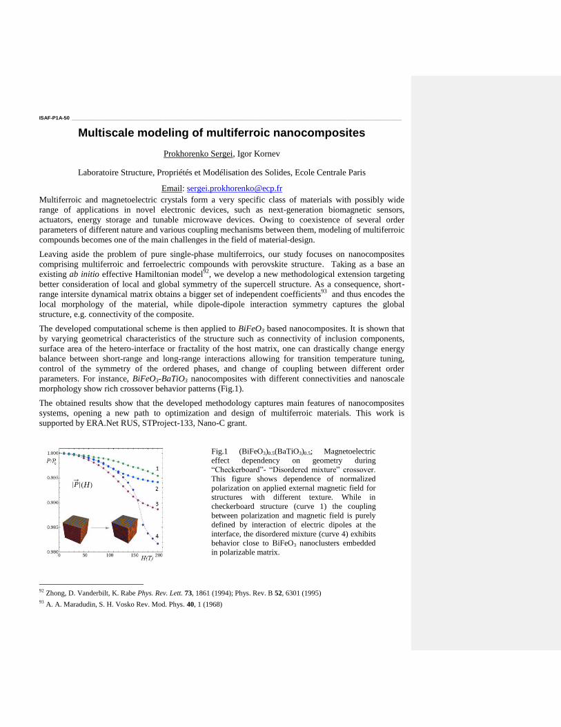
ISAF-P1A-50 ___________________________________________________________________________________________________________________
Multiscale modeling of multiferroic nanocomposites
Prokhorenko Sergei, Igor Kornev
Laboratoire Structure, Propriétés et Modélisation des Solides, Ecole Centrale Paris
Email: [email protected]
Multiferroic and magnetoelectric crystals form a very specific class of materials with possibly wide
range of applications in novel electronic devices, such as next-generation biomagnetic sensors,
actuators, energy storage and tunable microwave devices. Owing to coexistence of several order
parameters of different nature and various coupling mechanisms between them, modeling of multiferroic
compounds becomes one of the main challenges in the field of material-design.
Leaving aside the problem of pure single-phase multiferroics, our study focuses on nanocomposites
comprising multiferroic and ferroelectric compounds with perovskite structure. Taking as a base an
existing ab initio effective Hamiltonian model92
, we develop a new methodological extension targeting
better consideration of local and global symmetry of the supercell structure. As a consequence, short-
range intersite dynamical matrix obtains a bigger set of independent coefficients93
and thus encodes the
local morphology of the material, while dipole-dipole interaction symmetry captures the global
structure, e.g. connectivity of the composite.
The developed computational scheme is then applied to BiFeO3 based nanocomposites. It is shown that
by varying geometrical characteristics of the structure such as connectivity of inclusion components,
surface area of the hetero-interface or fractality of the host matrix, one can drastically change energy
balance between short-range and long-range interactions allowing for transition temperature tuning,
control of the symmetry of the ordered phases, and change of coupling between different order
parameters. For instance, BiFeO3-BaTiO3 nanocomposites with different connectivities and nanoscale
morphology show rich crossover behavior patterns (Fig.1).
The obtained results show that the developed methodology captures main features of nanocomposites
systems, opening a new path to optimization and design of multiferroic materials. This work is
supported by ERA.Net RUS, STProject-133, Nano-C grant.
Fig.1 (BiFeO3)0.5(BaTiO3)0.5; Magnetoelectric
effect dependency on geometry during
“Checkerboard”- “Disordered mixture” crossover.
This figure shows dependence of normalized
polarization on applied external magnetic field for
structures with different texture. While in
checkerboard structure (curve 1) the coupling
between polarization and magnetic field is purely
defined by interaction of electric dipoles at the
interface, the disordered mixture (curve 4) exhibits
behavior close to BiFeO3 nanoclusters embedded
in polarizable matrix.
92
Zhong, D. Vanderbilt, K. Rabe Phys. Rev. Lett. 73, 1861 (1994); Phys. Rev. B 52, 6301 (1995) 93
A. A. Maradudin, S. H. Vosko Rev. Mod. Phys. 40, 1 (1968)

PFM Poster
Forum Hall
Monday, July 22 2013, 01:00 pm - 04:30 pm
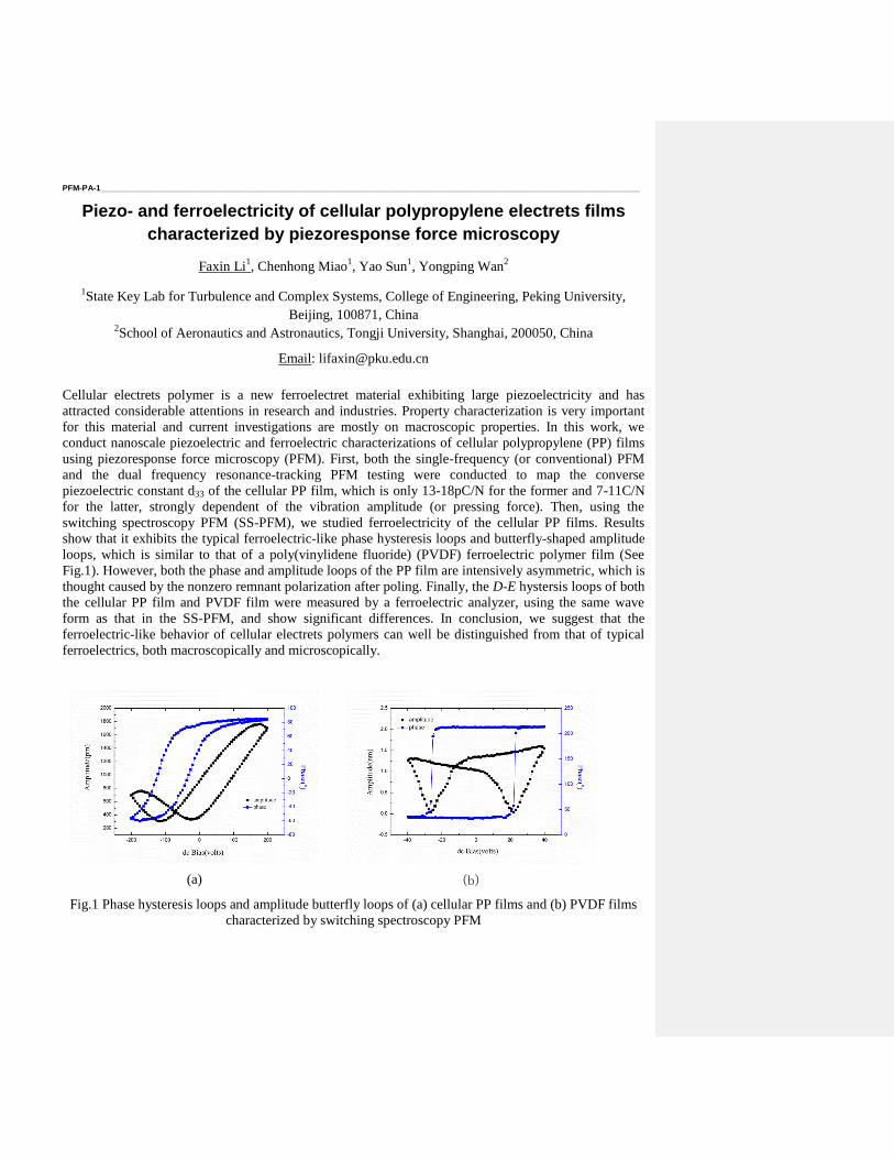
PFM-PA-1 ______________________________________________________________________________________________________________________
Piezo- and ferroelectricity of cellular polypropylene electrets films
characterized by piezoresponse force microscopy
Faxin Li1, Chenhong Miao
1, Yao Sun
1, Yongping Wan
2
1State Key Lab for Turbulence and Complex Systems, College of Engineering, Peking University,
Beijing, 100871, China 2School of Aeronautics and Astronautics, Tongji University, Shanghai, 200050, China
Email: [email protected]
Cellular electrets polymer is a new ferroelectret material exhibiting large piezoelectricity and has
attracted considerable attentions in research and industries. Property characterization is very important
for this material and current investigations are mostly on macroscopic properties. In this work, we
conduct nanoscale piezoelectric and ferroelectric characterizations of cellular polypropylene (PP) films
using piezoresponse force microscopy (PFM). First, both the single-frequency (or conventional) PFM
and the dual frequency resonance-tracking PFM testing were conducted to map the converse
piezoelectric constant d33 of the cellular PP film, which is only 13-18pC/N for the former and 7-11C/N
for the latter, strongly dependent of the vibration amplitude (or pressing force). Then, using the
switching spectroscopy PFM (SS-PFM), we studied ferroelectricity of the cellular PP films. Results
show that it exhibits the typical ferroelectric-like phase hysteresis loops and butterfly-shaped amplitude
loops, which is similar to that of a poly(vinylidene fluoride) (PVDF) ferroelectric polymer film (See
Fig.1). However, both the phase and amplitude loops of the PP film are intensively asymmetric, which is
thought caused by the nonzero remnant polarization after poling. Finally, the D-E hystersis loops of both
the cellular PP film and PVDF film were measured by a ferroelectric analyzer, using the same wave
form as that in the SS-PFM, and show significant differences. In conclusion, we suggest that the
ferroelectric-like behavior of cellular electrets polymers can well be distinguished from that of typical
ferroelectrics, both macroscopically and microscopically.
(a)
(b)
Fig.1 Phase hysteresis loops and amplitude butterfly loops of (a) cellular PP films and (b) PVDF films
characterized by switching spectroscopy PFM
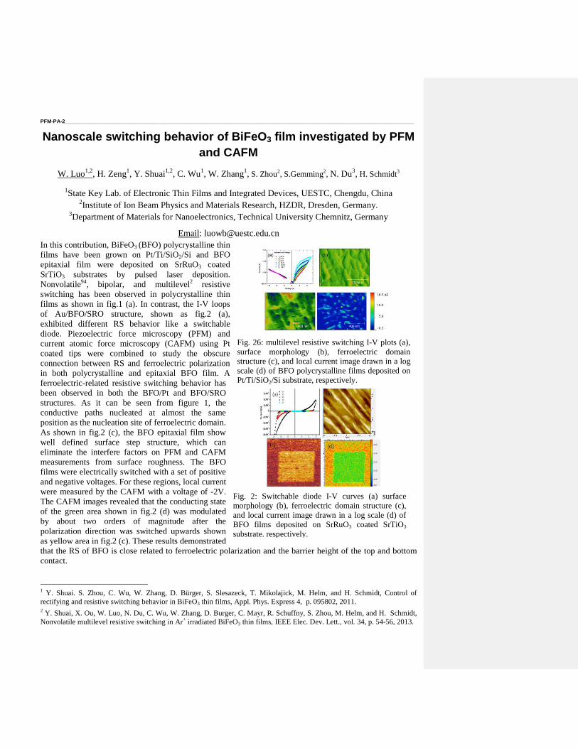
PFM-PA-2 ______________________________________________________________________________________________________________________
Nanoscale switching behavior of BiFeO3 film investigated by PFM
and CAFM
W. Luo1,2
, H. Zeng1, Y. Shuai
1,2, C. Wu
1, W. Zhang
1, S. Zhou
2, S.Gemming
2, N. Du
3, H. Schmidt
3
1State Key Lab. of Electronic Thin Films and Integrated Devices, UESTC, Chengdu, China
2Institute of Ion Beam Physics and Materials Research, HZDR, Dresden, Germany.
3Department of Materials for Nanoelectronics, Technical University Chemnitz, Germany
Email: [email protected]
In this contribution, BiFeO3 (BFO) polycrystalline thin
films have been grown on Pt/Ti/SiO2/Si and BFO
epitaxial film were deposited on SrRuO3 coated
SrTiO3 substrates by pulsed laser deposition.
Nonvolatile94, bipolar, and multilevel2 resistive
switching has been observed in polycrystalline thin
films as shown in fig.1 (a). In contrast, the I-V loops
of Au/BFO/SRO structure, shown as fig.2 (a),
exhibited different RS behavior like a switchable
diode. Piezoelectric force microscopy (PFM) and
current atomic force microscopy (CAFM) using Pt
coated tips were combined to study the obscure
connection between RS and ferroelectric polarization
in both polycrystalline and epitaxial BFO film. A
ferroelectric-related resistive switching behavior has
been observed in both the BFO/Pt and BFO/SRO
structures. As it can be seen from figure 1, the
conductive paths nucleated at almost the same
position as the nucleation site of ferroelectric domain.
As shown in fig.2 (c), the BFO epitaxial film show
well defined surface step structure, which can
eliminate the interfere factors on PFM and CAFM
measurements from surface roughness. The BFO
films were electrically switched with a set of positive
and negative voltages. For these regions, local current
were measured by the CAFM with a voltage of -2V.
The CAFM images revealed that the conducting state
of the green area shown in fig.2 (d) was modulated
by about two orders of magnitude after the
polarization direction was switched upwards shown
as yellow area in fig.2 (c). These results demonstrated
that the RS of BFO is close related to ferroelectric polarization and the barrier height of the top and bottom
contact.
1 Y. Shuai. S. Zhou, C. Wu, W. Zhang, D. Bürger, S. Slesazeck, T. Mikolajick, M. Helm, and H. Schmidt, Control of
rectifying and resistive switching behavior in BiFeO3 thin films, Appl. Phys. Express 4, p. 095802, 2011. 2 Y. Shuai, X. Ou, W. Luo, N. Du, C. Wu, W. Zhang, D. Burger, C. Mayr, R. Schuffny, S. Zhou, M. Helm, and H. Schmidt,
Nonvolatile multilevel resistive switching in Ar+ irradiated BiFeO3 thin films, IEEE Elec. Dev. Lett., vol. 34, p. 54-56, 2013.
Fig. 2: Switchable diode I-V curves (a) surface
morphology (b), ferroelectric domain structure (c),
and local current image drawn in a log scale (d) of
BFO films deposited on SrRuO3 coated SrTiO3
substrate. respectively.
Fig. 26: multilevel resistive switching I-V plots (a),
surface morphology (b), ferroelectric domain
structure (c), and local current image drawn in a log
scale (d) of BFO polycrystalline films deposited on
Pt/Ti/SiO2/Si substrate, respectively.
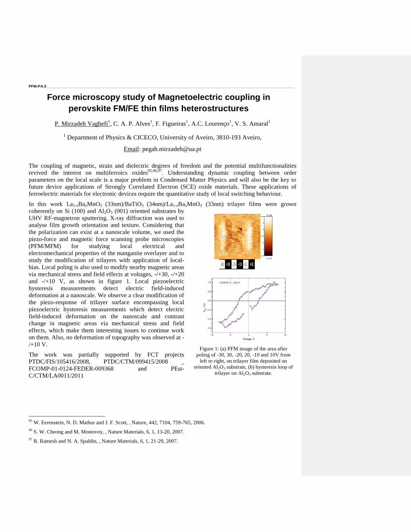
PFM-PA-3 ______________________________________________________________________________________________________________________
Force microscopy study of Magnetoelectric coupling in
perovskite FM/FE thin films heterostructures
P. Mirzadeh Vaghefi1, C. A. P. Alves
1, F. Figueiras
1, A.C. Lourenço
1, V. S. Amaral
1
1 Department of Physics & CICECO, University of Aveiro, 3810-193 Aveiro,
Email: [email protected]
The coupling of magnetic, strain and dielectric degrees of freedom and the potential multifunctionalities
revived the interest on multiferroics oxides95,96,97. Understanding dynamic coupling between order
parameters on the local scale is a major problem in Condensed Matter Physics and will also be the key to
future device applications of Strongly Correlated Electron (SCE) oxide materials. These applications of
ferroelectric materials for electronic devices require the quantitative study of local switching behaviour.
In this work La1-xBaxMnO3 (33nm)/BaTiO3 (34nm)/La1-xBaxMnO3 (33nm) trilayer films were grown
coherently on Si (100) and Al2O3 (001) oriented substrates by
UHV RF-magnetron sputtering. X-ray diffraction was used to
analyse film growth orientation and texture. Considering that
the polarization can exist at a nanoscale volume, we used the
piezo-force and magnetic force scanning probe microscopies
(PFM/MFM) for studying local electrical and
electromechanical properties of the manganite overlayer and to
study the modification of trilayers with application of local-
bias. Local poling is also used to modify nearby magnetic areas
via mechanical stress and field effects at voltages, -/+30, -/+20
and -/+10 V, as shown in figure 1. Local piezoelectric
hysteresis measurements detect electric field-induced
deformation at a nanoscale. We observe a clear modification of
the piezo-response of trilayer surface encompassing local
piezoelectric hysteresis measurements which detect electric
field-induced deformation on the nanoscale and contrast
change in magnetic areas via mechanical stress and field
effects, which make them interesting issues to continue work
on them. Also, no deformation of topography was observed at -
/+10 V.
The work was partially supported by FCT projects
PTDC/FIS/105416/2008, PTDC/CTM/099415/2008 _
FCOMP-01-0124-FEDER-009368 and PEst-
C/CTM/LA0011/2011
95
W. Eerenstein, N. D. Mathur and J. F. Scott, , Nature, 442, 7104, 759-765, 2006.
96 S. W. Cheong and M. Mostovoy, , Nature Materials, 6, 1, 13-20, 2007.
97 R. Ramesh and N. A. Spaldin, , Nature Materials, 6, 1, 21-29, 2007.
9.09
0.00
Figure 1: (a) PFM image of the area after
poling of -30, 30, -20, 20, -10 and 10V from
left to right, on trilayer film deposited on
oriented Al2O3 substrate, (b) hysteresis loop of
trilayer on Al2O3 substrate.
PFM-PA-4 ______________________________________________________________________________________________________________________
SPM study of localized magnetoelectric effect in
BaTiO3/Hexaferrite composite ceramics
Harsh Trivedi1, Vladimir V. Shvartsman
1, Doru C. Lupascu
1, Robert C. Pullar
2,3, Andrei Kholkin
2,3
1Institute for Materials Science, University of Duisburg-Essen, Essen, Germany
2CICECO, University of Aveiro, Aveiro, Portugal
3Department of Materials and Ceramic Engineering, University of Aveiro, Aveiro, Portugal
Email: [email protected]
Composite multiferroics are the materials with Piezoelectric and magnetostrictive constituent phases,
with an indirect stress mediated coupling at the interface resulting in a bulk magnetoelectric effect. As
compared to the single phase multiferroics the coupling in composites is usually large and exists at room
temperature, however due to general conducting nature of the magnetic phase in composites, bulk
measurements of ferroelectric properties is difficult. In this study, composite ceramics with a
homogeneous distribution of piezoelectric (BaTiO3) and magnetostrictive hexaferrite (BaFe12O19/
SrFe12O19) phases were investigated locally using Scanning Probe Microscopy (SPM) techniques like
MFM (Magnetic Force Microscopy) and PFM (Piezoresponse Force Microscopy). The domain patterns
of each constituent phase (Viz. Magnetic and Ferroelectric) were observed under applied conjugate
(Electric/Magnetic) fields and correlated with the virgin state of the domains. Apparent direct and
indirect coupling effects were observed in the form of restructuring of magnetic domain and changes in
the switching properties of ferroelectric domains. In the end an analysis for magnetic domain wall
motion is presented considering the Bloch-wall case.
PFM-PA-5 ______________________________________________________________________________________________________________________
Modulating domain wall conduction in epitaxial Pb(Zr0.2Ti0.8)O3
thin films by varying oxygen vacancy densities
Gaponenko Iaroslav1, Karthik Jambunathan
2, Martin Lane W.
2, Paruch Patrycja
1
1MaNEP-DPMC, University of Geneva, Geneva, Switzerland, CH-1205
2DMRL, University of Illinois, Urbana, IL, USA 61801
Email: [email protected]
Electrical conduction at domain walls in otherwise insulating ferroelectric or multiferroic materials has
been variously explained as intrinsic – with local structural changes decreasing the band gap [1],
extrinsic – where defects preferentially accumulating at domain walls allow a conduction pathway
across the sample [2], or as a dynamical phenomenon related to (ir)reversible microscopic displacements
of the domain walls in an applied electric field [3]. In particular in BiFeO3, recent studies have
highlighted the importance of oxygen vacancies for the observed conduction, both at domain walls [4]
and at more complex closure/vortex structures [5].
Here, we report on the significant role of oxygen vacancies in the domain wall conduction we
have previously demonstrated at 180° domain walls in epitaxial Pb(Zr0.2Ti0.8)O3 thin films [6]. For these
studies, we compare the conduction behavior of two different types of epitaxial PZT thin films grown on
SrRuO3 electrodes: the first grown by off-axis RF magnetron sputtering on SrTiO3 (STO), the second
grown by pulsed laser deposition (PLD) on DyScO3 (DSO). Both types of samples present a smooth
surface with a slightly granular morphology and a RMS roughness of 0.3 nm, but the Czochralski-grown
DSO substrates show higher crystalline quality and less dislocations than Verneuil-grown STO, and
present much lower densities of oxygen vacancies.
Using piezoresponse force microscopy (PFM) and conductive atomic force microscopy(c-AFM)
we show that contrary to the case of sputtered films, which show domain wall conduction as-grown, no
domain-wall-specific current is observed in the PLD grown films at low-medium voltages. At high
voltages, displacement currents related to the nucleation and growth of new domains are observed
throughout the whole sample, not specifically at the domain wall, together with static hot-spots of
localized current possibly related to pin-hole defects. However, after high-vacuum annealing of the
PLD-grown films at 300 °C for 30 minutes, domain wall conduction is recovered, and shows
qualitatively similar behavior to that observed in the sputtered films.
These results suggest that a threshold density of oxygen vacancies – naturally occuring in the
case of sputtered films, or engineered artificially for the PLD films – is needed for conduction at the
domain walls.
[1] J. Seidel et al, Nature Mater. 8, 229-234 (2009)
[2] J. Seidel et al, Phys. Rev. Lett. 105, 197603 (2010)
[3] P. Maksymovych et al, Nano Lett. 11, 1906 (2011)
[4] S. Farokhipoor et al, J. Appl. Phys. 112, 052003 (2012)
[5] N. Balke et al, Nature Physics 8, 81-88 (2012)
[6] J. Guyonnet et al, Adv. Mater. 23, 5377 (2011)
PFM-PA-6 ______________________________________________________________________________________________________________________
Piezoresponse force microscopy study of doped (K,Na)NbO3-
based ceramics for piezoactuator applications
Danka Gobeljic1, Vladimir Shvartsman
1, Ke Want
2, Wook Jo
3, Jing-Feng Li
2, Jürgen Rödel
3, Doru C.
Lupascu1
1Institute for Materials Science, Universität Duisburg-Essen, Essen, Germany
2State Key Laboratory of New Ceramics and Fine Processing, Tsinghua University, Beijing, P.R. China
3Institute of Materials Science, Technische Universität Darmstadt, Darmstadt, Germany
Email: [email protected]
A current development of potential lead-free alternatives to Pb(Zr,Ti)O3 (PZT) suggests (K,Na)NbO3
(KNN)-based materials as one of the most promising, lead-free piezoceramics. Owing to its excellent
electromechanical properties, particular dopants-modified KNN is suitable for high-precision,
temperature-stable actuator applications. Material, besides high piezoelectric constant d33, exhibits high
field-induced strain of significant stability in a range from room temperature up to 175 °C98
.
Here, we demonstrate results of a Piezoresponse Force Microscopy (PFM) study on
0.95(Na0.49K0.49Li0.02)(Nb0.8Ta0.2)O3-0.05CaZrO3 ceramics. Investigation of the temperature dependent
domain evolution, indicating a sequence of phase transformation responsible for enhanced piezoelectric
properties, is revealed. Correspondingly, locally obtained longitudinal piezoelectric coefficient shows
comparable temperature behavior as macroscopic small piezoelectric coefficient, d33.
Demonstrated study provides nanoscopic insight on mechanisms of enhanced electromechanical
properties in the studied KNN-based ceramics, establishing correlation with macroscopically determined
material properties.
98
K. Wang, F. Yao, W. Jo, D. Gobeljic, V. V. Shvartsman, D. C. Lupascu, J.F. Li and J. Rödel, “Temperature-Insensitive
(K,Na)NbO3-based Lead-free Piezo Actuator Ceramics”, Accepted by Adv. Funct. Mat. 2013.
PFM-PA-7 ______________________________________________________________________________________________________________________
PFM images of non-ferroelectric thin films
Borowiak Alexis1, Vilquin Bertrand
2, Baboux Nicolas
1, Brice Gautier
1
1Institut des Nanotechnologies de Lyon, INSA de Lyon, 20, avenue Albert Einstein, 69621 Villeurbanne, France
2Institut des Nanotechnologies de Lyon, Ecole Centrale de Lyon, 36 avenue Guy de Collongue, 69134 Ecully
cedex, France
Email: [email protected]
Piezoresponse Force Microscopy (PFM) is a powerful tool for the characterization of ferroelectric
materials thanks to its ability to map and control in a non destructive way domain structures in
ferroelectric films99
.
Most of the time, the ferroelectric behaviour of a film is tested by writing domains of opposite
polarisation with the Atomic Force Microscope (AFM) tip and/or by performing hysteresis loops with
the AFM tip as a top electrode. A given sample is declared ferroelectric when domains of opposite
direction have been detected, corresponding to zones of distinct contrast on the PFM image, or when an
open hysteresis loop is obtained. More prudently in certain cases, the ferroelectricity is at last attested
only when the contrast is stable within several hours100
.
But as the thickness of the films studied by PFM decrease, data become difficult to interpret. In
particular, charges trapped after current injection due to leakage currents may contribute in a non-
negligible way to the final contrast of PFM images. As a result a convincing PFM contrast has been
recently observed in non-ferroelectric oxides such as SrTiO3101
, (LaxSr1-x)MnO3102
and CaCu3Ti4O12103
.
This in not disturbing when the sample under consideration is known to be paraelectric but it may
become a real problem when very thin layers of a well-known ferroelectric material are under study.
It this communication, we will show that the standard procedure used in order to show the
ferroelectricity of a film can be applied to a non-ferroelectric sample with apparently the same results.
To do so, we use a LaAlO3 amorphous dielectric film and apply similar voltages as for artificially
written ferroelectric domains. The resulting pattern is imaged by PFM and exhibit zones of distinct PFM
contrasts, stable with time, similar to the one obtained with ferroelectric samples.
We will explain these results, try and choose the experimental parameters which minimize these effects,
and compare with results obtained on BaTiO3 thin films prepared by Molecular Beam Epitaxy which are
supposed to be ferroelectric. The aim of this study is to establish a reliable procedure which would
remove any ambiguity in the characterization of the ferroelectric nature of such samples.
99
A. Gruverman, O. Auciello, H. Tokumoto, “Scanning force microscopy for the study of domain structure in
ferroelectric thin films”, J. Vac. Sci. Technol. B., vol. 14 (2), p. 602-605, 1996. 100
V. Garcia, S. Fusil, K. Bouzehouane, S. Enouz-Vedrenne, N. D. Mathur, A. Barthélèmy, M. Bibes, “Giant tunnel
electroresistance for non-destructive readout of ferroelectric states”, Nature, vol. 460, p. 81-84, 2009. 101
A. Kholkin, I. Bdikin, T. Ostapchuk, J. Petzelt, “Room temperature surface piezoelectricity in SrTiO3 ceramics via
piezoresponse force microscopy”, Appl. Phys. Lett., vol. 93, 222905, 2008. 102
R. F. Mamin, I. K. Bdikin, A. L. Kholkin, “Locally induced charged states in La0.89Sr0.11MnO3 single crystals”,
Appl. Phys. Lett., vol. 94, 222901, 2009. 103
R. Tararam, I.K. Bdikin, N. Panwar, J. A. Varela, P. R. Bueno, A. L. Kholkin, “Nanoscale electromechanical
properties of CaCu3Ti4O12 ceramics”, J. Appl. Phys., vol. 110, 052019, 2011.
PFM-PA-8 ______________________________________________________________________________________________________________________
Morphological and Ferroelectric Studies of LiNbO3 Films Prepared
by a Sputtering Deposition
D.A. Kiselev, R.N. Zhukov, A.S. Bykov, M.D. Malinkovich, Yu.N. Parkhomenko
Department of the Material Science of Semiconductors and Dielectrics
National University of Science and Technology "MISiS"
Leninskiy pr. 4, 119049 Moscow, Russian Federation
Email: [email protected]
Lithium niobate (LiNbO3) has been one of the promising ferroelectric materials for potential
applications in the area of modulators, switches, actuators, surface acoustic wave devices, sensors, and
wave guides because of its high piezoelectric, photorefractive, and nonlinear optical properties.
However, thin films are advantageous over their bulk counterparts for various device applications. From
a technological point of view, the prospect of LiNbO3 thin films on Si substrates is particularly attractive
in view to combine the ferro- and piezoelectric processing capabilities of with lithium niobate the
obvious advantages of Si. Indeed, Si technology continues to dominate the microelectronics market,
providing a rigid substrate ideal for lithographic techniques. This will make possible the development of
integrated devices in which sources, detectors and electronics, as well as ferroelectric and waveguiding
components may be produced on the same wafer.
The studied LiNbO3 films were deposited by radio-frequencies magnetrom sputtering of the single-
crystalline target in Ar/O=1 atmosphere (0.6 Pa) on n-type Si (100) and Si (111) substrates ( = 2 Ω·cm)
with SiO2 buffer layer (thickness ~ 5 nm). The subsequent thermal annealing of the obtained structures
has been done in air at 700 ºС. Atomic force microscopy measurements indicate that the surface
roughness of the LiNbO3 thin films was 4-10 nm, which meets the demands for practical waveguiding
devices. The ferroelectric properties have been studied by visualization of the as-growth domain
structure (vertical and lateral component polarization), recording induced ferroelectric states and the
hysteresis loops by piezoresponse force microscopy (PFM) using Scanning probe laboratory NTEGRA-
Prima (NT MDT, Russia). Also, Kelvin probe force microscopy (KPFM) was used extensively for
determining electric properties in these heterostructures.
The research was financially supported by the Ministry of Education and Science of the Russian
Federation out using the equipment of Common-Use Scientific Center “Material Science and
Metallurgy” at NUST “MISiS” and by the Program for Creation and Development of the National
University of Science and Technology “MISiS”.
PFM-PA-9 ______________________________________________________________________________________________________________________
Local stress enhancement of ferroelectricity in GFO thin films
1Maksym Iazykov,
2Alexandre Thomasson,
1Brice Gautier,
2Natalie Viart
1 Institut des Nanotechnologies de Lyon, Villeurbanne/France
2 Institut de Physique et Chimie des Matériaux de Strasbourg, Strasbourg/France
Email: [email protected]
Today multiferroics become more and more attractive materials because of their fundamental ability to
combine ferroelectric and magnetic properties1. In recent years, multiferroics have been intensively
investigated. However, most of the reported materials demonstrate coupling of the magnetic and
ferroelectric order parameters at the temperatures much lower or higher than room temperature2,3
.
The promising candidate for potential application is Ga2−xFexO3 (GFO) oxides which show
ferromagnetic, ferroelectric and ferroelastic properties at near-ambient temperatures4,5
. This
phenomenon gives them great potential in technological application6,7
. However, physical properties of
GFO oxides have been proved for single-crystal samples whereas the device integration requires using
of thin films of these materials which were rarely reported until now8-10
.
In this work we performed local probe electrical characterization of GFO thin films. Conductive AFM
measurements showed strong leakage currents when sufficiently high voltages were applied to the
sample. This fact makes impossible domain switching by Piezoresponse Force Microscopy (PFM). The
direct mechanical domain writing has not provided switching of polarization. Despite this, we showed
that possible ferroelectricity of GFO can be studied using the Atomic Force Microscope (AFM) as
instrument for local stress enhancement of ferroelectricity. Such method allowed us relatively easy
writing of the ferroelectric domains avoiding the problem of the leakage currents. We hope that this
approach will lead to better understanding of current and capacitance measurements at the microscopic
level that is critical for possible improvement of the magnetoelectric properties of GFO. 1N.A. Hill, J. Phys. Chem. B 104, 6694, 2000
2A.M. dos Santos, S.Parashar, A.R.Raju et al, Solid State Comm. 122(1-2) 49-52, 2002
3N.Hur, S.Park , P.A.Sharma, J.S.Ahn, S.Guha and S.W.Cheong, Nature. 429 392–5, 2004
4J.P.Remeika, J. Appl. Phys. 31 263S, 1960
5G.T.Rado, Phys. Rev. Lett. 13 335, 1964
6J.H. Jung, M. Matsubara, T. Arima, J.P. He, Y. Kaneko, Y. Tokura, Phys.Rev. Lett. 93, 037 403, 2004
7 A.M. Kalashnikova, R.V. Pisarev, L.N. Bezmaternykh, V.L. Temerov, A. Kirilyuk, T. Rasing, JETP Lett. 81, 452, 2005
8D. C. Kundaliya, S. B. Ogale, S. Dhar, et al., J. Magn. Magn. Mater. 299 307-311, 2006
9Z. H. Sun, Y. L. Zhou, S. Y. Dai, et al., Appl. Phys. A: Mater. Sci. Process. 91 97-100, 2008
10M. Trassin, N. Viart, G. Versini, et al., Journal of Materials Chemistry 19 8876-8880, 2009
PFM-PA-10 _____________________________________________________________________________________________________________________
Buffer layer effect on microstructures and properties of Pb(Zr,Ti)O3-
CoFe2O4 layered thin films
Hongcai He, Feifei Luo, Neng Qian, Ning Wang
State Key Laboratory of Electronic Thin Films and Integrated Devices and School of Microelectronics
and Solid-State Electronics, University of Electronic Science and Technology of China, Chengdu
610054, P. R. China
Abstract:
The conductive oxide LaNiO3 thin film was selected as a buffer layer and a bottom electrode for the
Pb(Zr,Ti)O3-CoFe2O4 composite films derived from the sol–gel method in our previous work. This
LaNiO3 buffer obviously enhanced the magnetoelectric response of the Pb(Zr,Ti)O3–CoFe2O4 bi-layered
thin films. Deeper work will be introduced in this work. The LaNiO3 thin films with different thickness,
surface morphology, preferred orientation and conductivity are deposited on Si substrate as buffer layers
to deposite Pb(Zr,Ti)O3-CoFe2O4 composite films. XRD, SEM / EDS and AFM were used to
characterize films microstructure. Magnetic force microscopy (MFM) and piezo-force response
microscopy (PFM) were used to characterize the composite film at the local scale. Ferroelectric
hysteresis loops and ferromagnetic hysteresis loops were macroscopically measured. The direct ME
measurement was done in terms of the variation in the induced voltage by the applied magnetic field
using a self-made equipment. The results are compared and discussed in relation to the microstructure
and properties of LaNiO3 buffer layers.
Acknowledgement: This work has been supported by Natural Science Foundation of China (51002020,
51272035).
PFM-PA-11 _____________________________________________________________________________________________________________________
PFM study of size effects on lead-free ceramics and films of
(Bi0.5Na0.5)1-xBaxTiO3 with compositions around the morphotropic
phase boundary
Norberto Salazar1, Dulce Pérez-Mezcua
2, M. Lourdes Calzada
2, Adriana Gil
1, Jesús Ricote
2
1Nanotec Electrónica S.L., Tres Cantos, Madrid, Spain
2Instituto de Ciencia de Materiales de Madrid, CSIC, Madrid, Spain
Email: [email protected]
The increasing interest in the development of lead-free piezoelectric materials has drawn the attention to
solid solutions such as 1-x(Bi0.5Na0.5)TiO3-xBaTiO3 (BNBT). Enhanced dielectric, ferroelectric and
piezoelectric properties have been observed for bulk ceramics with compositions close to the
morphotropic phase boundary (MPB) between rhombohedral and tetragonal phases104
. The preparation
of these materials in thin film form is indispensable for their integration into microelectronic devices.
However a drastic decrease in the remnant polarization of BNBT thin films respect to their bulk
counterparts is reported105
. This has been attributed to size effects, as the reduction of dimensions in thin
films leads to smaller grains, which determines the nature of the ferroelectric domain configuration106
.
In order to understand the mechanisms that lead to the size effects responsible for the reduction of the
remnant properties, ceramics and films of BNBT with different grain sizes are analyzed by
Piezoresponse Force Microscopy. Materials are prepared from sol-gel derived solutions107
. The
comparison between the results obtained in micro- and nanometric grain size materials allows us to
discuss the effects of the grain size on the ferroelectric domain configuration, and to relate it to the
properties. Besides, the measurement of local piezoelectric loops and the study of the mobility of the
domain walls under an electric field will shed light onto the role of the grain boundaries. All
measurements were carried out with a Nanotec®
scanning force microscope.
104
T. Takenaka, K.I. Maruyama, K. Sakata, “(Bi1/2Na1/2)TiO3-BaTiO3 System for Lead-Free Piezoelectric Ceramics”, Jap. J.
Appl. Phys., vol 30, p. 2236-2239, 1991.
105 I. Bretos, D. Alonso-San José, R. Jiménez, J. Ricote, M.L. Calzada, “Evidence of morphotropic phase boundary
displacement in lead-free (Bi0.5Na0.5)1−xBaxTiO3 polycrystalline thin films”, Mater. Lett., vol 65, p. 2714-2716, 2011. 106
M. Algueró, J. Ricote, R. Jiménez, P. Ramos, J. Carreaud, J.M. Kiat, B. Dkhil, J. Holc, M. Kosec, “Size effect in
morphotropic phase boundary PbMg1/3Nb2/3O3–PbTiO3”, Appl. Phys. Lett., vol. 91, p. 112905, 2007.
107 D. Alonso-San José, R. Jiménez, I. Bretos, M.L. Calzada, “Lead-free ferroelectric (Na1/2Bi1/2)TiO3–BaTiO3 thin films in
the morphotropic phase boundary composition: solution processing and properties”, J. Amer. Ceram. Soc., vol. 92, p. 2218-
2225, 2009.
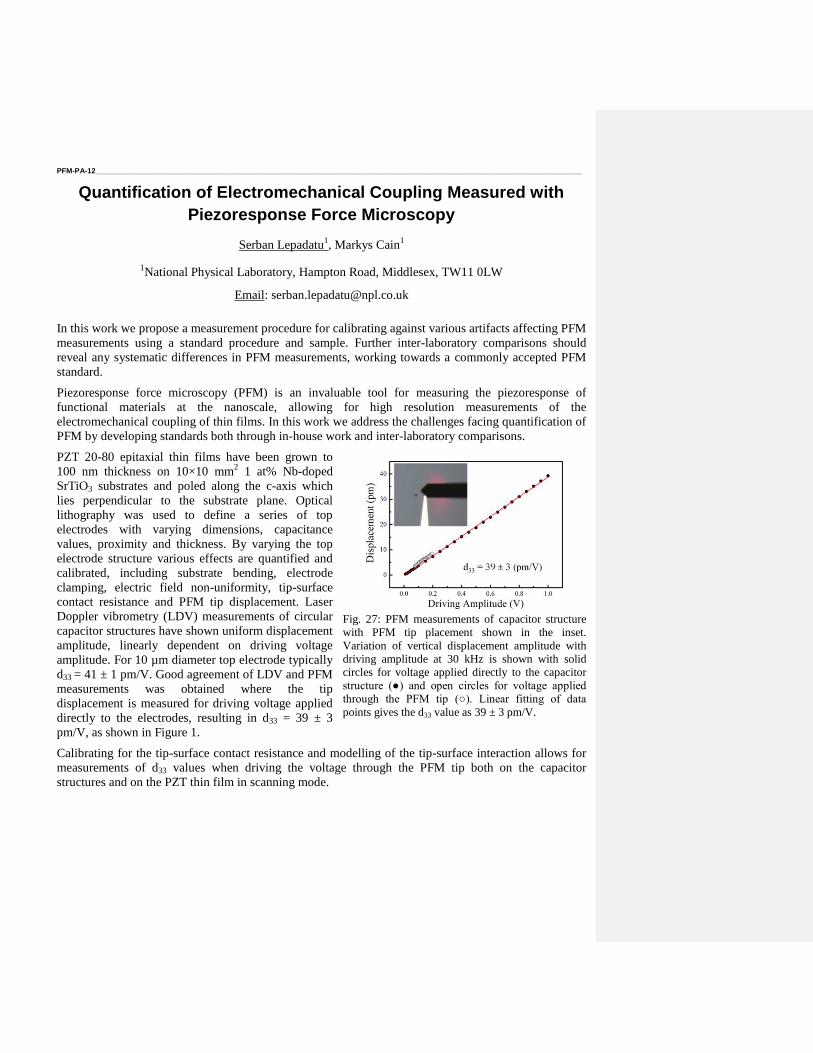
PFM-PA-12 _____________________________________________________________________________________________________________________
Quantification of Electromechanical Coupling Measured with
Piezoresponse Force Microscopy
Serban Lepadatu1, Markys Cain
1
1National Physical Laboratory, Hampton Road, Middlesex, TW11 0LW
Email: [email protected]
In this work we propose a measurement procedure for calibrating against various artifacts affecting PFM
measurements using a standard procedure and sample. Further inter-laboratory comparisons should
reveal any systematic differences in PFM measurements, working towards a commonly accepted PFM
standard.
Piezoresponse force microscopy (PFM) is an invaluable tool for measuring the piezoresponse of
functional materials at the nanoscale, allowing for high resolution measurements of the
electromechanical coupling of thin films. In this work we address the challenges facing quantification of
PFM by developing standards both through in-house work and inter-laboratory comparisons.
PZT 20-80 epitaxial thin films have been grown to
100 nm thickness on 10×10 mm2 1 at% Nb-doped
SrTiO3 substrates and poled along the c-axis which
lies perpendicular to the substrate plane. Optical
lithography was used to define a series of top
electrodes with varying dimensions, capacitance
values, proximity and thickness. By varying the top
electrode structure various effects are quantified and
calibrated, including substrate bending, electrode
clamping, electric field non-uniformity, tip-surface
contact resistance and PFM tip displacement. Laser
Doppler vibrometry (LDV) measurements of circular
capacitor structures have shown uniform displacement
amplitude, linearly dependent on driving voltage
amplitude. For 10 µm diameter top electrode typically
d33 = 41 ± 1 pm/V. Good agreement of LDV and PFM
measurements was obtained where the tip
displacement is measured for driving voltage applied
directly to the electrodes, resulting in d33 = 39 ± 3
pm/V, as shown in Figure 1.
Calibrating for the tip-surface contact resistance and modelling of the tip-surface interaction allows for
measurements of d33 values when driving the voltage through the PFM tip both on the capacitor
structures and on the PZT thin film in scanning mode.
Fig. 27: PFM measurements of capacitor structure
with PFM tip placement shown in the inset.
Variation of vertical displacement amplitude with
driving amplitude at 30 kHz is shown with solid
circles for voltage applied directly to the capacitor
structure (●) and open circles for voltage applied
through the PFM tip (○). Linear fitting of data
points gives the d33 value as 39 ± 3 pm/V.
PFM-PA-13 _____________________________________________________________________________________________________________________
Nanoscale piezoresponse and thermal behavior of ferroelectric domain in multiferroic BiFeO3 thin film
Huarong Zeng, Senxing Hui,Kunyu Zhao, Guorong Li, Qingrui Yin
Key Laboratory of Inorganic Functional Materials and Devices, Shanghai Institute of Ceramics, Chinese
Academy of Sciences, Shanghai 200050, China
Email: [email protected]
Multiferroic materials exhibit simultaneous ferroelectric and magnetic orders, which enable the coupling
interaction between ferroelectric and magnetic orders. This coupling interaction produces various
possibilities in the realization of mutual control and detection of electrical polarization and magnetism.
Recent advances of multiferroelectrics have offered an imperative need to develop high resolution tool
for in-situ investigating ferroelectric/ferromagnetic domain configurations and local physical properties.
Here we introduce piezoresponse force microscopy (PFM) and 3-scanning thermal microscopy (3-
SThM) to characterize local piezoresponse and thermal behavior of nanoscale domains in multiferroic
BiFeO3 (BFO) thin film. The 3-SThM, developed based on the customer-developed PFM, provides a
powerful tool for imaging locally thermal distributions and characterizing local thermal conductivity.
Ultrahigh resolution PFM imaging reveals that ferroelectric domain wall width is around 2.18 nm for
multiferroic BiFeO3 thin film, which is well consistent with the upper limit values of 2 nm via first
principle study [1]. Good polarization retention behavior was also demonstrated in the BFO thin film by
the PFM tip fields. Local thermal conductivity of ferroelectric domains of BFO thin film was firstly
performed by 3-SThM, and was found to be 1.525 W/mK. The local thermal conductivity dependence
of the domain switching behavior was also investigated and discussed in the present study.
PFM-PA-14 _____________________________________________________________________________________________________________________
The kinetics of the domain structure of TGS crystals investigated near
phase transition temperature by means of AFM
O.M.Golitsyna, V.O.Chulakova, S.N.Drozhdin
Voronezh State University / Voronezh / Russia
Email: [email protected]
Formation of the domain structure of triglycine sulfate crystals (TGS) after their rapid cooling
from the paraelectric to the ferroelectric phase is essentially non-equilibrium process, which has been
studied in detail 1,2
in the temperature range of stability of the spontaneous polarization PS, i.e. far from
the phase transition temperature TC. It is of interest to study this process in the vicinity of the phase
transition, where the fluctuations of PS can significantly affect the kinetics of forming and evolution of
the domain structure. The analysis of the literature shows that to date, such experimental studies have
not been carried out at temperatures close to TC. In this paper the evolution of the domain structure of
both nominally pure TGS and TGS doped with L,α-alanine was investigated at temperatures near TC.
The visualization of the domain structure of the polar cuts of these crystals was carried out by means
of atomic force microscopy (AFM) in contact mode of piezoelectric response (microscope Solver P47
Pro, cantilevers NSG 11/TiN). The samples were transferred into the paraelectric phase and after 30
minutes of exposure at ≈ 333 K cooled at a rate of 10 K / min to the desired temperature. The accuracy
of temperature stabilizing was equal to ± 0,05 K. At a given temperature T ≤ TC –1.0 K the evolution
of freshly formed domain structure was observed.
The kinetics of the formation of the domain structure was studied by means of calculations of the
space-time correlation function C (r, t) = <S(r,t)S(0,t)>, where S (r, t) = +1 or –1, depending on the sign
of the domain at the point with coordinate r. The following parameters of the domain structure also
were calculated:
1) average characteristic correlation length L, defined as the distance at which the correlation function
takes the value of C (r = L (t), t) = 1/2 with respect to its original value at r = 0, 2) the total perimeter of
the domain walls, 3) areas of the domains of opposite sign, and the coefficient of static unipolarity.
It was found that near TC the forming of a stable domain configuration occurs with a significantly
different kinetic parameters comparing with those calculated in 1,2
. It was found that the formation of
the domain structure in nominally pure and doped TGS is described by different kinetic parameters. The
general tendency of investigated processes of domain structure evolution is their slowing down with
the distance from the Curie temperature.
_____________________ 1 H.Orihara, N.Tomita, Y. Ishibashi. Ferroelectrics, vol.95, p.45-48, 1989.
2 V. Likodimos, M. Labardi, M. Allegrini. Physical Review B66, p.024104-1-02410407, 2002.
PFM-PA-15 _____________________________________________________________________________________________________________________
Piezo Force Microscopy as a Fundamental Tool for Characterization of Nanoporous PbTiO3 Thin Films
Alichandra Castro,1 Paula Ferreira,
1 Brian Rodriguez
2, Paula M. Vilarinho
1
1Department of Materials and Ceramic Engineering, University of Aveiro, Aveiro, Portugal
2Conway Institute of Biomolecular and Biomedical Research, University College Dublin, Dublin,
Ireland
Email: [email protected]
Nowadays, due to the increasing demand on portable electronic devices with ultrahigh density data storage
and lower power consumption, the miniaturization of the ferroelectric has become an important issue. This
progressive development requires the morphology control of materials and the understanding the effects of
size reduction on properties at the nanoscale, namely the ferroelectric properties. Within this context, we
have been exploiting nano and mesoporosity in ferroelectric materials, because ordered meso and nano
porous thin film arrays may be used as ferroelectric platforms for the conception of new multifunctional
materials, such as multiferroics. Multiferroics materials are currently of great interest for applications in
microelectronics. However, preparing nanoporous oxide thin films is not a trivial task and the influence of
porosity on the piezo and ferroelectric properties of these ferroelectric matrices is practically unknown. Due
to exceptional spatial resolution, Scanning Probe Microscopy (SPM) techniques and in particular
Piezoresponse Force Microscopy has become an important high resolution characterization tool for
visualization of domain structures in ferroelectric thin films at the nanoscale.
Thus, in this work, Vertical Piezoresponse Force Microscopy (VPFM), Lateral Piezoresponse Force
Microscopy (LPFM), and Switching Spectroscopy Piezoresponse Force Microscopy (SSPFM) are used to
characterize the piezoelectric and ferroelectric properties of mesostructured PbTiO3 thin films prepared by
sol-gel and evaporation-induced self-assembly methodologies.108 The porous PbTiO3 thin films were
thermally treated at different temperatures in order to assess the effect of the microstructure crystallization
evolution on the ferroelectric properties and the results obtained for nanoporous thin films are compared with
PbTiO3 dense thin films prepared under the same conditions. Scanning electron microscopy (SEM) and PFM
results clearly demonstrate the existence of two distinct areas, which exhibit different crystallinity and
consequently different local piezoelectric properties. The area with strong out-of-plane piezoresponse
increases with the thermal treatment temperature, as well as the tetragonal phase. In addition, at a more local
scale it is also observed that the regions near the pores exhibit a higher piezoresponse that is possibly
associated with a higher degree of crystallinity in these regions. The ferroelectric behaviour in these samples
was also demonstrated by the typical square-shaped piezoelectric hysteresis loops. Some of these hysteresis
loops exhibit imprint and the relation between this vertical and lateral shift is related to the processing
conditions and porosity. We evaluated also the piezoelectric and switching properties in different grains
using PFM and SS-PFM. The size influence of each grains on electric properties was discussed as a function
of coercive bias, imprint voltage and saturation response. Microstructural details were analyzed by Scanning
Electron Microscopy (SEM), Transmission Electron Microscopy and Ultra-Raman. X-ray diffraction (XRD)
analyses were used to characterize the phase content, lattice parameters and mesoporosity.
Acknowledgements
The authors thank FCT and FEDER (QREN – COMPETE) for funding the project PTDC/CTM/098130/2008
and to the FCT for the Doctoral fellowship SFRH/BD/67121/2009. We thank also to the COST Action
MP0904 SIMUFER for funding the STSM in Dublin.
108
P. Ferreira, R. Z. Hou, A. Wu, M.-G. Willinger, P. M. Vilarinho, J. Mosa, C. Laberty-Robert, C. Boissière, D. Grosso, C.
Sanchez, “Nanoporous Piezo- and Ferroelectric Thin Films”, Langmuir, vol. 28, p. 2944-2949, 2012.
PFM-PA-16 _____________________________________________________________________________________________________________________
Local Polarization Reversal
in the Vicinity of 180o Domain Wall in Lithium Niobate
Ievlev Anton1, Shur Vladimir
1, Neradovskiy Maxim
1, Turigin Anton
1,
Morozovska Anna2, Eliseev Eugene
2, and Kalinin Sergei
3
1Ferroelectric Laboratory, Ural Federal University, Ekaterinburg, Russia
2Lashkaryov Institute of Semiconductor Physics, National Academy of Sciences of Ukraine,
Kiev, Ukraine 3The Center for Nanophase Materials Sciences and Technology Division,
Oak Ridge National Laboratory, Oak Ridge, TN, USA
Email: [email protected]
Local polarization reversal under the action of local electric field produced by conductive tip of
scanning probe microscope has been studied in the vicinity of the existing flat domain wall in 30-m-
thick single crystalline plate of periodically poled congruent lithium niobate (CLN). The polarization
reversal has been carried out on different distances from existing domain wall.
Two modes of tip motion between switching points were used. Non-contact mode represents tip motion
at distance about 2 m over the sample surface. Polarization reversal at distances above 250 nm from
the wall led to formation of isolated domains (Fig 1a) with linear dependence of radius on pulse
amplitude. Switching at distance < 250 nm from the wall led to round shaped shifts of the wall
(Fig. 1b,c). Contact mode uses the motion of the grounded tip in contact with the surface. Formation of
prolate triangular shifts (length 350 nm) (Fig 1d) and nanodomain chains with period 100 nm (Fig 1e,f)
was observed for the tip motion across the wall.
The observed domain kinetics has been explained by polarization reversal under the action of residual
depolarization filed and stimulation of polarization reversal along the path of grounded SPM tip due to
effective external screening. Analytical and numerical simulations of the spatial distribution of residual
depolarization field in the vicinity of the isolated needle-like domain justified the proposed model.
Figure 1. Domain structures formed as a result of local switching near the flat 180o domain wall. (a) isolated
domains; (b), (c) round-shaped shifts of the wall; (d) prolate triangular shift; (e), (f) nanodomain chains.
The equipment of the UCSU “Modern Nanotechnology”, Institute of Natural Sciences, UrFU has been
used. The research was made possible in part by RFBR (Grants 12-02-31377-mol-a, 13-02-01391-а, 11-
02-91066-CNRS-а), by Ministry of Education and Science (Сontracts 14.513.12.0006 and
16.740.11.0585).
PFM-PA-17 _____________________________________________________________________________________________________________________
Size effect of the space charge modulation in semiconductor
caused by ferroelectric domain structure
Anna N. Morozovska,1 Eugene A. Eliseev,
2 Olexander V. Varenyk
3, and
Sergei V. Kalinin4,
1 Institute of Physics, National Academy of Sciences of Ukraine,
41, pr. Nauki, 03028 Kiev, Ukraine 2 Institute for Problems of Materials Science, National Academy of Sciences of Ukraine,
3, Krjijanovskogo, 03142 Kiev, Ukraine
3 Taras Shevchenko
Kiev National University, Radiophysical Faculty
4g, pr. Akademika Hlushkova, 03022 Kiev, Ukraine 4 The Center for Nanophase Materials Sciences, Oak Ridge National Laboratory,
Oak Ridge, TN 37831
Email: [email protected]
We consider a typical heterostructure “domain patterned ferroelectric film ultra-thin physical gap
(dielectric layer) semiconductor (electrolyte)”, where the semiconductor can be an incipient
ferroelectric, high-k narrow-gap semiconductors, covered with water adsorbents. Unexpectedly we have
found that the space charge modulation profile and amplitude in the semiconductor, that screens the
spontaneous polarization of a 180-degree domain structure of ferroelectric, nonlinearly depends on the
domain structure period a, dielectric layer thickness h and semiconductor screening radius Rd in a rather
non-trivial way. Multiple size effects appearance and manifestation are defined by the relationship
between a, h and Rd. Under the absence of the dielectric layer the space charge amplitude very slows
saturates to a spontaneous polarization value with the domain size increase. When the dielectric layer is
present, the amplitude saturates to the smaller values, at that the saturation value essentially decreases
with the layer thickness increase, but the saturation rate is almost independent on the thickness in the
actual range of parameters. The space charge amplitude strongly vanishes with the dielectric thickness
increase only for small domain period, but remains almost constant for wide domains. We show that the
concept of effective gap h* can be introduced in a simple way only for a single-domain limit. Depth
distribution of electric potential is nonlinear inside ferroelectric, while it is linear inside the dielectric
and exponentially vanishes inside the semiconductor as anticipated. Obtained exact analytical results
open the way for understanding of complex current-AFM measurements of contaminated ferroelectric
surfaces in ambient atmosphere with moderate humidity.
PFM-PA-18 _____________________________________________________________________________________________________________________
Study of ferroelectric nanodomains in epitaxial PbTiO3 films by
PFM and Raman spectroscopy
Fedir Borodavka1, Ivan Gregora
1, Ausrine Bartasyte
2, Samuel Margueron
3 and Jiří Hlinka
1
1Institute of Physics, Prague, Czech Republic
2Institute Jean Lamour, Nancy, France
3Université de Lorraine and Supélec, Metz, France
Email: [email protected]
Investigation of the domain structure in ferroelectric thin films is helpful for elucidating the interfacial
processes in these materials and for finding possible ways of their applications.
Domain structure of 320 nm thin films of ferroelectric lead titanate (PTO) grown using the metalorganic
chemical vapour deposition method (MOCVD) on TbScO3(TSO) and SmScO3(SSO) perovskite
substrates have been studied with the help of piezoresponse force microscopy (PFM) and Raman
spectroscopy techniques.
PFM (Fig.1) and Raman show that PTO films grown on SSO have preferentially a-domain orientation
(in-plane orientation of spontaneous polarization PS), while films grown on TSO substrate have
dominantly c-domain orientation (out-of-plane orientation of PS). The striking difference between the
two domain structures can be assigned to the opposite sign of the epitaxial misfit strain at the deposition
temperature 650°C (a'TSO< a'PTO <a'SSO).
Fig. 28: PFM images of 320 nm thin PbTiO3 film on SmScO3 (a) and TbScO3 (b) substrates. Edges of the
scanned area are roughly parallel to pseudocubic axes of the substrate.
PFM-PA-19 _____________________________________________________________________________________________________________________
Li diffusion and electrochemical activity in commercial LiMn2O4
battery cathode by Electrochemical Strain Microscopy
Sergey Luchkin1, Andrei Kholkin
1, Nina Balke
2
1Dept. of Materials and Ceramics Engng. & CICECO, University of Aveiro, 3810-193 Aveiro, Portugal 2The Center for Nanophase Materials Science, Oak Ridge National Laboratory, Oak Ridge, Tennessee
37831, USA
Email: [email protected]
Fast growth of popularity of green technologies leads to a wider use of Li batteries in applications that
require high power density. High charging and discharging rates result in intensive degradation of
battery materials. Deep understanding of the degradation mechanisms associated with Li transport is
essential to engineer new battery materials with long life and excellent reliability. These studies should
be done on a nanoscale to identify the defect sites responsible for degradation.For this, we used
Electrochemical Strain Microscopy (ESM) [1] , a technique similar to Piezoresponse Force Microscopy
(PFM) where ionic diffusion is responsible for measurable surface displacements. Li diffusivity and
electrochemical activity was studied in commercial LiMn2O4 cathodes. Typical cathode consists of
LiMn2O4 oxide particles and conductive carbon black particles distributed in PVDF binder. In the
cathodes we observed clear ESM response on the active oxide particles that is a representation of the
local molar volume change caused by Li diffusion. Conductive nanoparticle distribution in the binder
PVDF was detected by PFM. We used both the ESM time voltage spectroscopes to measure
electrochemical activity of Li ions on the active particles. The obtained results are discussed based on
the current understanding of Li diffusion mechanism in Li cathode materials. This research was
supported by the European project «Nanomotion» (FP7-People-2011-ITN-290158). The authors
gratefully acknowledge A. Hugues-Yanis and D. Rosato (Robert Bosch GmbH) for providing samples
and valuable discussions.
1. A. N. Morozovska, E. A. Eliseev, N. Balke, and S. V. Kalinin, «Local probing of ionic diffusion by
electrochemical strain microscopy: Spatial resolution and signal formation mechanisms», J. Appl. Phys.
108, 053712, 2010.
PFM-PA-20 _____________________________________________________________________________________________________________________
Nanoscale Crystallization of Piezoelectric Polymer and
Its Electromechanical Properties Studied by
Atomic Force Microscopy
Gun Ahn1,2
, Seungbum Hong1,2
,Kwangsoo No1
1Department of Materials and Science Engineering, KAIST, South Korea
2Nanoscience and Technology Division, Argonne National Laboratory, USA
Email: [email protected], [email protected]
Piezoelectric polymers have attracted great attentions due to its potential applications to bio-compatible
actuators, wireless sensors, and energy harvesting devices. However, the crystallization process and
subsequent electrical poling, which are essential in realizing such devices, have been the most difficult
challenges. Here, we suggest a novel method to control the crystallization process by using atomic force
microscopy (AFM) equipped with a nanoscale tip of various coatings, which we can use to confine the
mechanical load, electrical field and temperature gradient. Furthermore, we will present the AFM tip-
induced nanoscale crystallization under different ambient condition by changing the purging gas into a
sealed sample holder to study the impact of surrounding gas or water molecules on the
electromechanical properties of the piezoelectric polymers.
PFM-PA-21 _____________________________________________________________________________________________________________________
Measurement Anomaly of Step Width using
Atomic Force Microscopy
Gun Ahn1,2
, Dean J. Miller3, Kwangsoo No
2, Seungbum Hong
1,2
1Nanoscience and Technology Division, Argonne National Laboratory, USA
2Department of Materials and Science Engineering, KAIST, South Korea
3Electron Microscopy Center, Argonne National Laboratory, USA
Email: [email protected], [email protected]
We imaged the topography of silicon grating having a pitch of 10 µm with different pixel pitch to find
the optimum resolution using atomic force microscopy (AFM). We found that the step width decreased
from 1300 to 108 nm and the step height increased from 172 to 184 nm when a pixel pitch in fast scan
axis decreased from 625 nm to 3.9 nm. We also measured the step width and height of etched silicon
grating by a focused ion beam (FIB) using Scanning Electron Microscopy (SEM) and compared the
measured step height and width with AFM data. The obtained values from SEM image were 187.3 nm ±
6.2 nm and 116 nm ± 10.4 nm,which were in agreement with AFM data with 39 nm and 23 nm of pixel
pitches, respectively. Lastly, our findings that RMS roughness varied less than 1 nm and converged at
the value of 77.6 nm with any pixel pitch suggest we can use the RMS roughness obtained with any
resolution. Based on the assumption that our results scale linearly with the size of the features of
interest, we believe that one can use the optimal pixel resolution for fast and reliable topography
acquisition and surface roughness analysis.
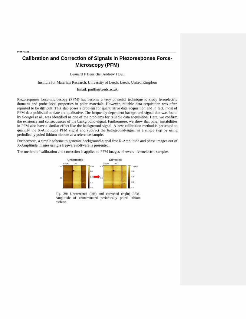
PFM-PA-22 _____________________________________________________________________________________________________________________
Calibration and Correction of Signals in Piezoresponse Force-
Microscopy (PFM)
Leonard F Henrichs, Andrew J Bell
Institute for Materials Research, University of Leeds, Leeds, United Kingdom
Email: [email protected]
Piezoresponse force-microscopy (PFM) has become a very powerful technique to study ferroelectric
domains and probe local properties in polar materials. However, reliable data acquisition was often
reported to be difficult. This also poses a problem for quantitative data acquisition and in fact, most of
PFM data published to date are qualitative. The frequency-dependent background-signal that was found
by Soergel et al., was identified as one of the problems for reliable data acquisition. Here, we confirm
the existence and consequences of the background-signal. Furthermore, we show that other instabilities
in PFM also have a similar effect like the background-signal. A new calibration method is presented to
quantify the X-Amplitude PFM signal and subtract the background-signal in a single step by using
periodically poled lithium niobate as a reference sample.
Furthermore, a simple scheme to generate background-signal free R-Amplitude and phase images out of
X-Amplitude images using a freeware software is presented.
The method of calibration and correction is applied to PFM images of several ferroelectric samples.
Fig. 29: Uncorrected (left) and corrected (right) PFM-
Amplitude of contaminated periodically poled lithium
niobate.
PFM-PA-23 _____________________________________________________________________________________________________________________
Roger Proksch1
1Asylum Research, USA
Piezoresponse Force Microscopy (PFM) and Electrochemical Strain Microscopy (ESM) have led to significant progress in
our understanding of the nano-electromechanical origins of functionality in a large variety of materials. For example,
hysteresis has been considered the “smoking gun” that demonstrates ferroelectricity in PFM measurements. The cantilever is
an extended mechanical object with normal modes that depend on the boundary conditions both of the cantilever structure
itself and on the boundary conditions imposed by the tip-sample interactions. By using the encoded and motorized optical
beam controls on a commercial microscope we have been able to directly measure the extended shape of the cantilever as it
interacts with various samples and in a variety of measurement modes. Integration of the laser scanning mechanism directly
in the AFM has enabled these shape measurements during normal AFM operation in a variety of imaging modes ranging
from force curves and contact modes to AC modes. This presentation will focus on contact and force curves measurement
modes. In many cases of interest, the response of a cantilever does not behave as a simple, single-mode system. To elucidate
the effects of local and long-ranged drive mechanisms on the multi-modal cantilever probe, the response of the cantilever as a
function of both frequency and optical beam spot position has been measured in-situ while the cantilever is directly probing a
functional material, either with PFM or ESM. Two interesting results are (i) the crossover between the dc and first contact
mode is measurable at surprisingly low frequencies, and (ii) contrary to initial expectations, operating on resonance actually
provides more stable and reliable quantification of the cantilever drive. This is explained in terms of the high Q-factor of the
resonance. The crossover frequency is affected by the boundary conditions, specifically the tip-sample stiffness. Because of
this, electrochemical interactions at the tip can lead to a measured change in the amplitude and phase of the cantilever, even
when the response of the sample remains unchanged. In particular, this in turn can cause measured 180 degree phase shifts in
the measured response. This phase shift – stemming from a change in the tip-sample stiffness – is indistinguishable from a
phase shift originating from a change in the polarization of the sample. We will show simulations and experimental data that
illustrate this crosstalk. In addition, we will discuss methods to remove separate these two effects.

ISAF Student poster competition Forum Hall
Monday, July 22 2013, 01:00 pm - 02:00 pm
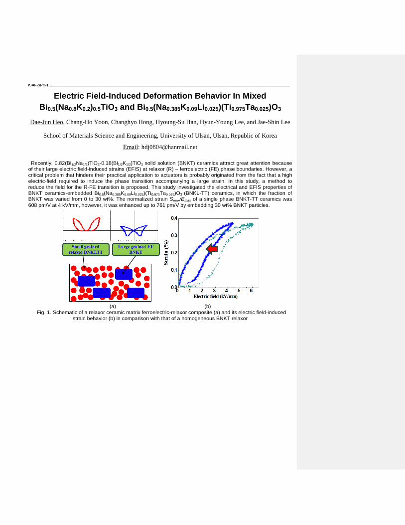
ISAF-SPC-1 ____________________________________________________________________________________________________________________
Electric Field-Induced Deformation Behavior In Mixed
Bi0.5(Na0.8K0.2)0.5TiO3 and Bi0.5(Na0.385K0.09Li0.025)(Ti0.975Ta0.025)O3
Dae-Jun Heo, Chang-Ho Yoon, Changhyo Hong, Hyoung-Su Han, Hyun-Young Lee, and Jae-Shin Lee
School of Materials Science and Engineering, University of Ulsan, Ulsan, Republic of Korea
Email: [email protected]
Recently, 0.82(Bi1/2Na1/2)TiO3-0.18(Bi1/2K1/2)TiO3 solid solution (BNKT) ceramics attract great attention because of their large electric field-induced strains (EFIS) at relaxor (R) – ferroelectric (FE) phase boundaries. However, a critical problem that hinders their practical application to actuators is probably originated from the fact that a high electric-field required to induce the phase transition accompanying a large strain. In this study, a method to reduce the field for the R-FE transition is proposed. This study investigated the electrical and EFIS properties of BNKT ceramics-embedded Bi0.5(Na0.385K0.09Li0.025)(Ti0.975Ta0.025)O3 (BNKL-TT) ceramics, in which the fraction of BNKT was varied from 0 to 30 wt%. The normalized strain Smax/Emax of a single phase BNKT-TT ceramics was
608 pm/V at 4 kV/mm, however, it was enhanced up to 761 pm/V by embedding 30 wt% BNKT particles.
(a) (b)
Fig. 1. Schematic of a relaxor ceramic matrix ferroelectric-relaxor composite (a) and its electric field-induced strain behavior (b) in comparison with that of a homogeneous BNKT relaxor
ISAF-SPC-2 ____________________________________________________________________________________________________________________
Temperature Dependence of Domain Contributions to
Piezoelectric Activity in the Soft- & Hard-doped Lead Zirconate
Titanate and La-doped Bismuth Ferrite Lead Titanate Systems
Sayyed Adam Qaisar1, Andrew J Bell
2, Timothy P Comyn
3
1Institute for Materials Research, University of Leeds, Leeds, United Kingdom
Email: [email protected]
Previous investigations have established the significance of the Rayleigh law to explaining intrinsic and
extrinsic contributions to activity in piezoelectric ceramics[1–4]. Typically investigations of domain wall
contributions to the piezoelectric effect require the use of synchrotron time. Presented is a technique using a
combination of weak-signal & direct-effect measurements in addition to electrical characterization to elude
to the reversible and irreversible domain contributions to the piezoelectric effect in lead zirconate titanate
(PZT) and bismuth ferrite lead titanate (BFPT) systems.
A new experimental apparatus has been constructed, allowing for investigation of cycling electric field &
stress effects at selected temperatures on the degradation of d33 in piezoelectric materials. Furthermore, the
device has been used to investigate the intrinsic and extrinsic contributions to the direct piezoelectric effect
in PZT & La-doped BFPT. Supported by using weak-signal measurements, the domain wall behaviour and
piezoelectric activity at elevated temperatures has been investigated for these material systems in addition to
activity degradation.
Data from the new apparatus is presented and further discussed in relation to previously observed behaviour
in PZT[5][6][7], highlighting the enhanced mechanical properties of BFPT over PZT and comparing the
temperature dependence of domain contributions in both material systems
[1] D. Damjanovic and M. Demartin, Journal of Physics: Condensed Matter, vol. 9, no. 23, pp. 4943–
4953, Jun. 1997.
[2] R. E. Eitel, T. R. Shrout, and C. A. Randall, Journal of Applied Physics, vol. 124110, 2006.
[3] A. Pramanick, D. Damjanovic, J. E. Daniels, J. C. Nino, and J. L. Jones, Journal of the American Ceramic Society, vol. 94, no. 2, pp. 293–309, Feb. 2011.
[4] M. Davis, D. Damjanovic, and N. Setter, Journal of Applied Physics, vol. 084103, 2006.
[5] J. Nuffer, Acta Materialia, vol. 48, no. 14, pp. 3783–3794, Sep. 2000.
[6] H. Wang, A. a. Wereszczak, and H.-T. Lin, Journal of Applied Physics, vol. 105, no. 1, p. 014112, 2009.
[7] M. Liu and K. J. Hsia, Applied Physics Letters, vol. 83, no. 19, p. 3978, 2003.
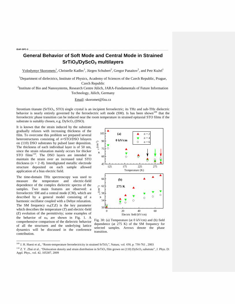
ISAF-SPC-3 ____________________________________________________________________________________________________________________
General Behavior of Soft Mode and Central Mode in Strained
SrTiO3/DyScO3 multilayers
Volodymyr Skoromets1, Christelle Kadlec
1, Jürgen Schubert
2, Gregor Panaitov
2, and Petr Kužel
1
1Department of dielectrics, Institute of Physics, Academy of Sciences of the Czech Republic, Prague,
Czech Republic 2Institute of Bio and Nanosystems, Research Centre Jülich, JARA-Fundamentals of Future Information
Technology, Jülich, Germany
Email: [email protected]
Strontium titanate (SrTiO3, STO) single crystal is an incipient ferroelectric; its THz and sub-THz dielectric
behavior is nearly entirely governed by the ferroelectric soft mode (SM). Is has been shown109 that the
ferroelectric phase transition can be induced near the room temperature in strained epitaxial STO films if the
substrate is suitably chosen, e.g. DyScO3 (DSO).
It is known that the strain induced by the substrate
gradually relaxes with increasing thickness of the
film. To overcome this problem we prepared several
heterostructures consisting of n×STO/DSO bilayers
on (110) DSO substrates by pulsed laser deposition.
The thickness of each individual layer is of 50 nm,
since the strain relaxation mainly occurs for thicker
STO films110. The DSO layers are intended to
maintain the strain over an increased total STO
thickness (n = 2–8). Interdigitated metallic electrode
structure deposited on each sample allowed
application of a bias electric field.
The time-domain THz spectroscopy was used to
measure the temperature and electric-field
dependence of the complex dielectric spectra of the
samples. Two main features are observed: a
ferroelectric SM and a central mode (CM), which are
described by a general model consisting of a
harmonic oscillator coupled with a Debye relaxation.
The SM frequency 0(T,E) is the key parameter
which describes the temperature (T) and electric-field
(E) evolution of the permittivity; some examples of
the behavior of 0 are shown in Fig. 1. A
comprehensive comparison of the dielectric behavior
of all the structures and the underlying lattice
dynamics will be discussed in the conference
contribution.
109
J. H. Haeni et al., “Room-temperature ferroelectricity in strained SrTiO3”, Nature, vol. 430, p. 758-761 , 2003 110
Z. Y. Zhai et al., “Dislocation density and strain distribution in SrTiO3 film grown on (110) DyScO3 substrate”, J. Phys. D:
Appl. Phys., vol. 42, 105307, 2009
125 175 225 275
Temperature (K)
105
90
75
60
45
0 (
cm
-1)
n = 2
n = 4
n = 6
0 20 40 60
Electric field (kV/cm)
66
62
58
54
50
0 (
cm
-1)
(a)
(b)
0 kV/cm
275 K
Fig. 30: (a) Temperature (at 0 kV/cm) and (b) field
dependence (at 275 K) of the SM frequency for
selected samples. Arrows denote the phase
transition.
ISAF-SPC-4 ____________________________________________________________________________________________________________________
Fabrication and characterization of BaTiO3 ultrathin ferro-electric layers to investigate the origin and characteristics of domain wall
conductivity.
Alan Douglas1, Li-Wu Chang
1, Marty Gregg
1
1Centre for Nanostructured Media, Queens University Belfast, Belfast, Northern Ireland
Email: [email protected]
An investigation into the fabrication and characterization of ferroelectric heterostructures was carried
out. The materials of choice were a combination of ultrathin Barium Titanate (BTO) and Strontium
Ruthenate (SRO), a ferroelectric and bottom electrode layer respectfully; these layers were deposited on
a substrate of Strontium Titanate (STO) by Pulsed Laser Deposition (PLD).
The films were then characterized by in-house measurements through Atomic Force Microscopy
(AFM), Piezoresponse Force Microscopy (PFM), Transmission Electron Microscopy (TEM), and X-Ray
Diffraction (XRD). Such techniques allowed the fabrication method to continually be adapted until the
production high quality ultra-thin ferroelectric BTO films was achieved.
Domains and domain walls within the ultrathin ferroelectric layer were then investigated using both
PFM and Scanning Tunneling Microscopy (STM), with the intention of being able to measure domain
wall conductivity and investigate the factors which control conductivity. The use of STM has not been
widely utilized for domain wall studies111
but should allow both high-resolution conductivity mapping
and direct probing of the densities of states within the domain walls.
Striving for a better understanding and control over ferroelectric domain walls will no doubt prove of
use, as it will enable us to better integrate such components into an newly emerging generation of
nanoscale electronic devices.
1. Chiu, Y.P. et al. "Atomic-Scale Evolution of Local Electronic Structure Across Multiferroic Domain Walls." Advanced
Materials 23, 1530–1534 (2011).
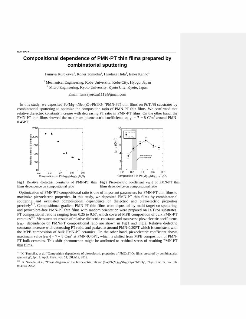
ISAF-SPC-5 ____________________________________________________________________________________________________________________
Compositional dependence of PMN-PT thin films prepared by
combinatorial sputtering
Fumiya Kurokawa1, Kohei Tomioka
2, Hirotaka Hida
1, Isaku Kanno
1
1 Mechanical Engineering, Kobe University, Kobe City, Hyogo, Japan
2 Micro Engineering, Kyoto University, Kyoto City, Kyoto, Japan
Email: [email protected]
In this study, we deposited Pb(Mg1/3Nb2/3)O3-PbTiO3 (PMN-PT) thin films on Pt/Ti/Si substrates by
combinatorial sputtering to optimize the composition ratio of PMN-PT thin films. We confirmed that
relative dielectric constants increase with decreasing PT ratio in PMN-PT films. On the other hand, the
PMN-PT thin films showed the maximum piezoelectric coefficients |e31,f | = 7 ~ 8 C/m2
around PMN-
0.45PT.
Optimization of PMN/PT compositional ratio is one of important parameters for PMN-PT thin films to
maximize piezoelectric properties. In this study, we deposited PMN-PT thin films by combinatorial
sputtering and evaluated compositional dependence of dielectric and piezoelectric properties
precisely112
. Compositional gradient PMN-PT thin films were deposited by multi target co-sputtering,
and pyrochlore-free PMN-PT thin films with random orientation were prepared on Pt/Ti/Si substrates.
PT compositional ratio is ranging from 0.25 to 0.57, which covered MPB composition of bulk PMN-PT
ceramics113
. Measurement results of relative dielectric constants and transverse piezoelectric coefficients
|e31,f | dependence on PMN/PT compositional ratio are shown in Fig.1 and Fig.2. Relative dielectric
constants increase with decreasing PT ratio, and peaked at around PMN-0.30PT which is consistent with
the MPB composition of bulk PMN-PT ceramics. On the other hand, piezoelectric coefficient shows
maximum value |e31,f | = 7 ~ 8 C/m2 at PMN-0.45PT, which is shifted from MPB composition of PMN-
PT bulk ceramics. This shift phenomenon might be attributed to residual stress of resulting PMN-PT
thin films.
112
K. Tomoika, et al, “Composition dependence of piezoelectric properties of Pb(Zr,Ti)O3 films prepared by combinatorial
sputtering”, Jpn. J. Appl. Phys., vol. 51, 09LA12, 2012. 113
B. Noheda, et al, “Phase diagram of the ferroelectric relaxor (1-x)Pb(Mg1/3Nb2/3)O3-xPbTiO3”, Phys. Rev. B., vol. 66,
054104, 2002.
Fig.1 Relative dielectric constants of PMN-PT thin
films dependence on compositional ratio Fig.2 Piezoelectric coefficient |e31,f | of PMN-PT thin
films dependence on compositional ratio
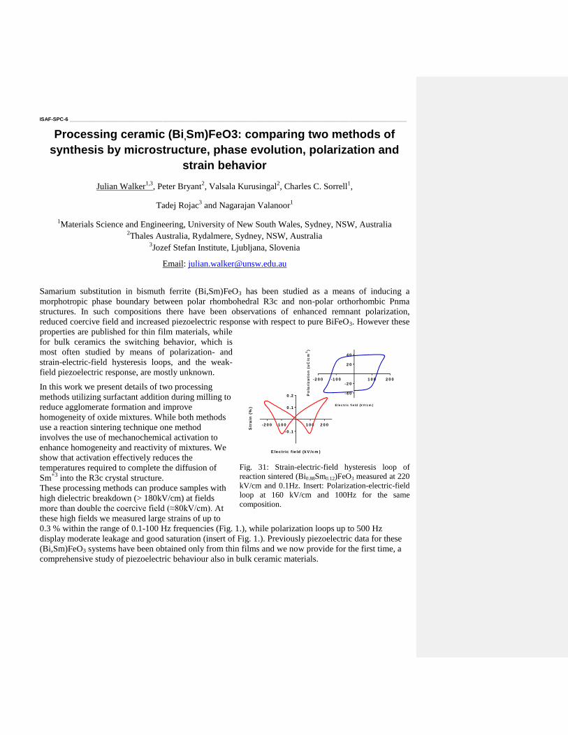
ISAF-SPC-6 ____________________________________________________________________________________________________________________
Processing ceramic (Bi,Sm)FeO3: comparing two methods of
synthesis by microstructure, phase evolution, polarization and
strain behavior
Julian Walker1,3
, Peter Bryant2, Valsala Kurusingal
2, Charles C. Sorrell
1,
Tadej Rojac3 and Nagarajan Valanoor
1
1Materials Science and Engineering, University of New South Wales, Sydney, NSW, Australia
2Thales Australia, Rydalmere, Sydney, NSW, Australia
3Jozef Stefan Institute, Ljubljana, Slovenia
Email: [email protected]
Samarium substitution in bismuth ferrite (Bi,Sm)FeO3 has been studied as a means of inducing a
morphotropic phase boundary between polar rhombohedral R3c and non-polar orthorhombic Pnma
structures. In such compositions there have been observations of enhanced remnant polarization,
reduced coercive field and increased piezoelectric response with respect to pure BiFeO3. However these
properties are published for thin film materials, while
for bulk ceramics the switching behavior, which is
most often studied by means of polarization- and
strain-electric-field hysteresis loops, and the weak-
field piezoelectric response, are mostly unknown.
In this work we present details of two processing
methods utilizing surfactant addition during milling to
reduce agglomerate formation and improve
homogeneity of oxide mixtures. While both methods
use a reaction sintering technique one method
involves the use of mechanochemical activation to
enhance homogeneity and reactivity of mixtures. We
show that activation effectively reduces the
temperatures required to complete the diffusion of
Sm+3
into the R3c crystal structure.
These processing methods can produce samples with
high dielectric breakdown (> 180kV/cm) at fields
more than double the coercive field (≈80kV/cm). At
these high fields we measured large strains of up to
0.3 % within the range of 0.1-100 Hz frequencies (Fig. 1.), while polarization loops up to 500 Hz
display moderate leakage and good saturation (insert of Fig. 1.). Previously piezoelectric data for these
(Bi,Sm)FeO3 systems have been obtained only from thin films and we now provide for the first time, a
comprehensive study of piezoelectric behaviour also in bulk ceramic materials.
E le c tric fie ld (k V /c m )
Str
ain
(%
)
-2 0 0 -1 0 0 1 0 0 2 0 0
-0 .1
0 .1
0 .2
E le c tr ic f ie ld (k V /c m )
Po
lariz
ati
on
(u
C/c
m2)
-2 0 0 -1 0 0 1 0 0 2 0 0
-4 0
-2 0
2 0
4 0
Fig. 31: Strain-electric-field hysteresis loop of
reaction sintered (Bi0.88Sm0.12)FeO3 measured at 220
kV/cm and 0.1Hz. Insert: Polarization-electric-field
loop at 160 kV/cm and 100Hz for the same
composition.
ISAF-SPC-7 ____________________________________________________________________________________________________________________
Textured K0.5Na0.5NbO3 thin films by aqueous chemical solution
deposition on SrTiO3 substrates
Ky-Nam Pham1, Maxim Morozov
1, Thomas Tybell
2, Tor Grande
1, Mari-Ann Einarsrud
1
1 Department of Material Science and Engineering, Norwegian University of Science and Technology,
Trondheim, Norway 2Department of Electronics and Telecommunications, Norwegian University of Science and
Technology, Trondheim, Norway
Email: [email protected]
The search for lead-free alternatives to PZT materials is currently going on worldwide. Na0.5K0.5NbO3
(KNN) thin films were fabricated on (100) and (110) oriented SrTiO3 substrates by chemical solution
deposition. Stable environmentally friendly aqueous KNN precursor solutions were prepared from Na-
acetate, K-acetate and Nb-ammonium oxalate and deposited onto SrTiO3/Nb:SrTiO3 substrates by spin
coating at 2500-3000 rpm for 20-40 s. The films were dried at 200 oC for 2 min using a hotplate and
then pyrolysed at 400 oC for 5 min. The film thickness could be controlled by repeating the spin coating
procedure. The final films were sintered at 600-900 oC for 5 min in oxygen by rapid thermal processing
(RTP) with heating rate of 40 oC/s. To aid texturing of the KNN-based films, Dissolution/reprecipitation
of KNN in a molten mixture of NaCl/KCl was tested to enhance texturing by incorporating salts in the
solution or deposition of salt layers between the KNN layers, which could be washed away after the
thermal treatment.
Homogeneous films with an average grain size down to 60 nm were prepared after heat treatment at 900 oC. The high degree of texture was confirmed by XRD, Fig. a). The intensity of the KNN (100)
reflection for films on (100) oriented substrates increased with increasing sintering temperature up to
900 oC, while for KNN films deposited on (110)-oriented substrate the (110) reflect that texture could be
controlled by the crystal orientation of the substrate.
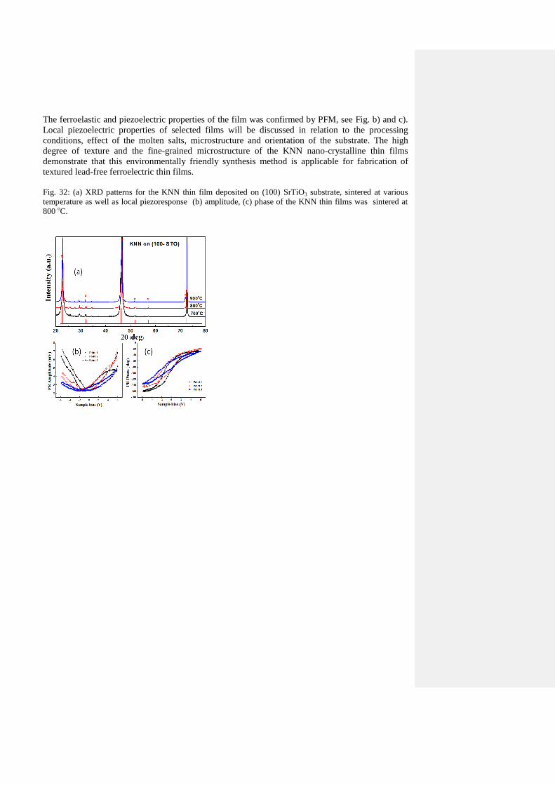
The ferroelastic and piezoelectric properties of the film was confirmed by PFM, see Fig. b) and c).
Local piezoelectric properties of selected films will be discussed in relation to the processing
conditions, effect of the molten salts, microstructure and orientation of the substrate. The high
degree of texture and the fine-grained microstructure of the KNN nano-crystalline thin films
demonstrate that this environmentally friendly synthesis method is applicable for fabrication of
textured lead-free ferroelectric thin films.
Fig. 32: (a) XRD patterns for the KNN thin film deposited on (100) SrTiO3 substrate, sintered at various
temperature as well as local piezoresponse (b) amplitude, (c) phase of the KNN thin films was sintered at
800 oC.
ISAF-SPC-8 ____________________________________________________________________________________________________________________
Growth and Piezo-/Ferroelectric Properties of Pb(Mg1/3Nb2/3)O3-
PbTiO3-Bi(Zn1/2Ti1/2)O3 Ternary Single Crystals
Reagan Belan, Hamel Tailor, Zuo-Guang Ye
Department of Chemistry and 4D LABS, Simon Fraser University,
Burnaby, BC, V5A 1S6, Canada
Email: [email protected]
Single crystals of relaxor-based perovskite solid solutions, namely Pb(Mg1/3Nb2/3)O3–PbTiO3
[PMN-PT] and Pb(Zn1/3Nb2/3)O3–PbTiO3 [PZN-PT], show extraordinary piezoelectric performance,
enabling them to be the leading choice of materials for the next generation of electromechanical
transducers in a broad range of applications1. However, these materials suffer from some
drawbacks, in particular, a low Curie temperature (TC) and a low coercive field (Ec). In order to
overcome these shortages, Bi(Zn1/2Ti1/2)O3 [BZT] was added to ‘harden’ the PMN-PT system and
the ternary solid solution system of Pb(Mg1/3Nb2/3)O3‒PbTiO3‒Bi(Zn1/2Ti1/2)O3 [PMN‒PT‒BZT]
was prepared in our laboratory in the form of ceramics and single crystals2,3
. In this work, we report
the growth of the single crystals of this ternary solid solution by the high temperature solution
(flux) method using a PbO and H2BO3 mixture as flux. By varying both the temperature profile of
the growth and the nominal composition of charge, large and good-quality multinucleated crystals
of PMN‒PT‒BZT were obtained. The domain structure and phase transitions of the PMN‒PT‒BZT
crystals are characterized by polarized light microscopy (PLM) and piezoresponse force microscopy
(PFM), providing insights into the crystal growth behavior of the ternary system. The dielectric and
ferroelectric properties of the crystals are also investigated, confirming that the ternary single
crystals exhibit enhanced piezoelectric performance compared to their ceramic counterparts.
This work is supported by the Office of Naval Research (Grants No. N00014-11-1-0552 and
N00014-12-1-1045) and the Natural Science and Engineering Research Council of Canada.
1Z.-G. Ye, Mater. Res. Soc. Bull., Vol. 34, No. 4 , pp. 277-283 (2009).
2H. N. Tailor, A. A. Bokov, Z.-G. Ye, Ferroelectrics, 405, 67-75 (2010).
3R. Belan, H. N. Tailor, X. Long, A. A. Bokov and Z.-G. Ye, J. Cryst. Growth, 318, 839-845 (2011)
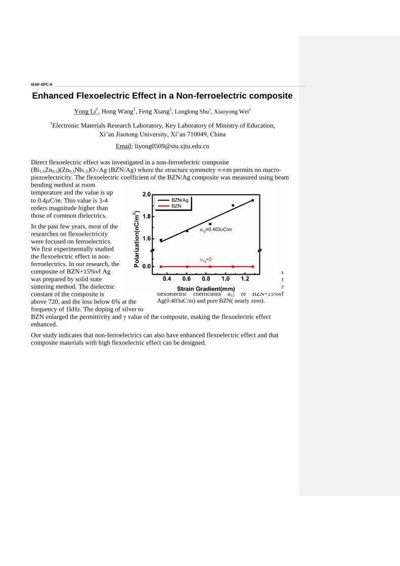
ISAF-SPC-9 ____________________________________________________________________________________________________________________
Enhanced Flexoelectric Effect in a Non-ferroelectric composite
Yong Li1, Hong Wang
1, Feng Xiang
1, Longlong Shu
1, Xiaoyong Wei
1
1Electronic Materials Research Laboratory, Key Laboratory of Ministry of Education,
Xi’an Jiaotong University, Xi’an 710049, China
Email: [email protected]
Direct flexoelectric effect was investigated in a non-ferroelectric composite
(Bi1.5Zn0.5)(Zn0.5Nb1.5)O7/Ag (BZN/Ag) where the structure symmetry ∞∞m permits no macro-
piezoelectricity. The flexoelectric coefficient of the BZN/Ag composite was measured using beam
bending method at room
temperature and the value is up
to 0.4C/m. This value is 3-4
orders magnitude higher than
those of common dielectrics.
In the past few years, most of the
researches on flexoelectricity
were focused on ferroelectrics.
We first experimentally studied
the flexoelectric effect in non-
ferroelectrics. In our research, the
composite of BZN+15%vf Ag
was prepared by solid state
sintering method. The dielectric
constant of the composite is
above 720, and the loss below 6% at the
frequency of 1kHz. The doping of silver to
BZN enlarged the permittivity and γ value of the composite, making the flexoelectric effect
enhanced.
Our study indicates that non-ferroelectrics can also have enhanced flexoelectric effect and that
composite materials with high flexoelectric effect can be designed.
Fig. 1: The linear fit of flexoelectric polarization as
a function of applied strain gradient measured at
23℃.The slopes of the lines are separately the
flexoelectric coefficients u12 of BZN+15%vf
Ag(0.403uC/m) and pure BZN( nearly zero).
ISAF-SPC-10 ___________________________________________________________________________________________________________________
High frequency magneto-impedance effects in multiferroic CoTiO2-Bi4Ti3O12 multilayer films
Hanae Kijima1,3
, Zhang Yiwen1, Nobukiyo Kobayashi
2, Shigehiro Ohnuma
1, 2,Nava Setter
3, Paul
Muralt3
and Hiroshi Masumoto1
1 Center for Interdisciplinary Research, Tohoku University, Sendai, Japan 2 Research Institute for Electromagnetic Materials RIEM, Sendai, Japan
3 Laboratoire de Céramique, Ecole Polytechnique Fédérale de Lausanne EPFL, Lausanne, Switzerland
Email: [email protected]
Multiferroic thin film structures are of great interest for applications in the lower GHz frequency
range. In our study, we combine soft magnetic thin films exhibiting a strong magneto impedance
(MI) effect with ferroelectric thin films. The impedance change upon application of an external
magnetic field (Hex) is supposed to occur also in magnetic-ferroelectric multilayers. It is expected
that the MI effect can be suitably enhanced at magnetic resonances occurring at a few GHz.
In expectation of high permeability (μ) and dielectric permittivity
(ε) at GHz frequencies, CoTiO2 and Bi4Ti3O12 are selected for the
soft magnetic and dielectric layers, respectively. In this study, we
present a strong resonance effect in µ measurements, and a
significant magneto-impedance effect in CoTiO2- Bi4Ti3O12
multilayer films in the frequency range of 0.1-10 GHz at room
temperature.
50 nm thick ferromagnetic CoTiO2 layers were intercalated with
Bi4Ti3O12 dielectric thin films. Both were grown by rf magnetron
sputtering. The frequency dependence of μ was investigated by
using the shielded parallel line method in the frequency range of
0.1-10 GHz. The Hex was applied parallel to rf-magnetic field in the
film plane. For the high frequency impedance analysis, micro MIM
capacitors were fabricated by lithography and wet etching
processes. The complex admittance (Y = G+iB) of the film under
various Hex were measured by using calibrated 50 Ohm probes for
the desired frequency range. The measurements are carried out at
room temperature.
Figure 1 presents the frequency dependence of real and imaginary
part of μ, and G and B of CoTiO2- Bi4Ti3O12 multilayer films at
various H-fields Hex. The μ” shows a clear peak at the
ferromagnetic resonance (fr) at 3.76 GHz. The intensity of the peak
decreases from 94.8 to nearly zero when applying a Hex of 334 Oe.
Interestingly, G and B values around fr also change with varying
Hex. The maximum increase of B (by 12.3 %) was observed at 3.76
GHz in a magnetic field of Hex = 96 Oe.
Acknowledgement
We wish to thank Dr. S. Takada for his cooperation of high
frequency μ measurement. The authors would like to thank for
much help and technical assistance of Mr. R. M. Aghdam (EPFL),
Fig. 33: The frequency
dependence of μ’(a), μ” (b), G
(c) and B(d) measured at
various values of Hex.

Mr. M. Murakami (RIEM) and Mr. M. Iwasa (RIEM).
ISAF-SPC-11 ___________________________________________________________________________________________________________________
Large and stable actuation strain by reversible 90o domain switching in 0.62%PMN-0.38%PT crystal under electromechanical
loading Yingwei Li, Faxin Li
State Key Lab for Turbulence and Complex Systems, College of Engineering, Peking University,
Beijing, 100871, China
Email: [email protected]
Ferroelectric actuators are characterized by their peculiar electromechanical energy conversion
efficiency, ultra-fast response, and compact size, etc. However, their wide application is limited by
the small piezoelectric strains of ferroelectric materials. Therefore, intensive efforts have been made
in this aspect. The biggest breakthrough was achieved by Park and Shrout in 1990s. They obtained
large actuation strains of ~1.7% in relaxor ferroelectric crystals via phase transformation.
However, the actuation ability of relaxor ferroelectric crystals decreases to 0.2~0.4% within the
up-operation field limit in the vicinity of 1.5~2.0kV/mm. Large reversible actuation strains of
~0.8% were also realized by using the huge strain accompanied with 90o domain switching via
point-defect mediation or via electromechanical loading. For the former, further investigations
concerned its stability is still needed before utilizing due to the intrinsic dissipation property of the
point defects. As for the latter, their practical applications were inconvenienced by the compressive
stress sensitivity of the actuation strains, the brittleness of BaTiO3 crystals, and the requirement of
large bipolar field power amplifier. Here we report that a pre-poled 0.62%PMN-0.38PT crystal can
generate large strains of 0.65% at uni-polar electric fields of 1.8kV/mm with uniaxial pre-
compression. Such large strains stem from the reversible 90o domain switching under the
competition between compressive stresses and electric fields. Additionally, the actuation strain is
stable. It only decreases about 7.7% after one thousand cycle’s electric fields loading. On the other
hand, the actuation strains can be larger than 0.42% in a wide range of compressive stresses
(12MPa~40MPa). These characteristics make it suitable for practical applications.
Fig 1. (a) Electric field vs. strain (E-S) curves for PMN-PT crystal during unipolar electric fields
loading at different levels of compressive stress, (b) Evolution of the electric field vs. strain curve
under cycle’s electric fields loading (The compressive stress is at 20MPa).

ISAF-SPC-12 ___________________________________________________________________________________________________________________
A MEMS AlN transducer array for use as a cochlear implant
Katherine Knisely and Karl Grosh
Mechanical Engineering, University of Michigan, Ann Arbor, MI
Email: [email protected]
Aluminum nitride (AlN) has emerged as an excellent material for a variety of MEMS applications
because of its high electrical resistance, low dielectric loss, and high sound velocity. Recently,
MEMS sensors using AlN in a bimorph cantilever configuration have been demonstrated with low
noise floors and good sensitivity114
. Because of its very low dielectric loss factor and relatively
simple deposition process as a thin film, AlN is an excellent material for microphones. The
cantilever configuration has many benefits, including a more linear response, control of the
frequency response using simple changes to the beam geometry, and simple adaptation from
microphone to hydrophone.
We present an array of AlN bimorph cantilevers, fabricated using MEMS batch processing
techniques, with applications both as a hydrophone array and as a completely implantable cochlear
implant (CI). A silicon backbone supports five 400μm wide, 5μm thick bimorph
(Platinum/aluminum nitride (AlN) stack) cantilevers, each of which is designed to have a
resonance, in water, that corresponds to its tonotopic location
in the guinea pig cochlea (20-40kHz). A 1mm wide, 10μm
thick parylene and gold ribbon cable extends 3cm from the
probe to an electrode bay, where electrical connections to
each cantilever are accessed. The frequency response of a
cantilever in a viscous fluid is predicted using a modified
Euler-Bernoulli equation that includes fluid loading and
viscous damping115
, and is measured in air using a laser
vibrometer and in water using a calibrated underwater
transducer pair.
Unlike traditional CIs, this probe is designed to transduce
mechanical vibrations of the cochlear fluid into electrical
signals that stimulate the auditory nerves without the use of an
external sound processing unit. Vibrations in the cochlear
fluid deflect the cantilevers, resulting in a potential forming
on the outer electrode layers of the cantilever. The outer
electrodes are in electrical contact with the ionic fluid of the cochlea, producing a current in the
cochlear fluid that is passed to the auditory nerves. In this design the energy is locally sensed and
converted into stimulation within the cochlea, therefore our design does not require the traditional
signal processing unit, microphone, and transceiver that current CIs employ. Benefits of this design
include lower power, smaller size, and lower latency when compared with current commercial CIs.
114
R. Littrell and K. Grosh, Journal of Microelectromechanical Systems 21(2), 406 (2012). 115
JE Sader. Journal of. Applied Physics, 84:64–76, 1998.
Fig. 34: The fabricated device. The
cantilever array (left, circled, with a
closeup on the right ) is connected to
an electrode bay for external electrical
monitoring by a flexible parylene-gold
ribbon cable.

ISAF-SPC-13 ___________________________________________________________________________________________________________________
Piezoelectric Films for High Density Switching Arrays for Logic
R. Keech
1, S. Shetty
1, S. Trolier-McKinstry
1, D. Newns
2, and G. Martyna
2
1Department of Materials Science and Engineering, Pennsylvania State University
Millennium Sciences Complex, State College, PA, 16802 2IBM TJ Watson Research Center
Yorktown Heights, PA 10598
A fast, low power, transistor-type switching device has been proposed in which piezoelectric and
piezoresistive materials are employed in a stacked sandwich structure of nanometer dimension.
Of particular interest to this program is the functionality of the high aspect ratio piezoelectric
70Pb(Mg1/3Nb2/3)O3-30PbTiO3 (PMN-PT) component. Dense PMN-PT films of approximately
350 nm in thickness were made by a 2MOE solvent sol-gel route. These films were phase pure
and strongly 100 oriented by XRD with dielectric constants exceeding 1300 and loss tangents of
approximately 0.01. The films showed slim hysteresis loops with remanent polarizations of about
10 μC/cm2 and breakdown field of over 1500 kV/cm. The films exhibited large signal strain of
over 1% with clamped, large signal d33,f of approximately 90 nm/V. Reactive ion etching (RIE)
has been employed to pattern features in the PMN-PT film down to one micron in spatial scale
with vertical sidewalls. Upon lateral scaling, a small increase in small signal electrical properties
has been observed. The paper will describe the evolution in properties that develop as the films
are further laterally subdivided into small driving pixels.
Corresponding author:
Ryan R. Keech
Department of Material Science and Engineering
Pennsylvania State University
N-225 Millennium Science Complex
State College, PA, 16801
Phone: (207) 651-8804
E-mail: [email protected]
ISAF-SPC-14 ___________________________________________________________________________________________________________________
Pb(In1/2Nb1/2)-Pb(Mg1/3Nb2/3)-PbTiO3 single crystal monomorph
with perpendicular electrode connections for sensing and
energy harvesting
Ming Ma, Zhenrong Li, Zhuo Xu, Xi Yao
Electronic Materials Research Laboratory, Key Laboratory of Education Ministry; International
Center for Dielectric Research, Xi’an Jiaotong University, Xi’an 710049, China
Email: [email protected]
Piezoelectric monomorph, which has only one element, is one kind of potential structure for
piezoelectric applications in some extreme conditions. However the traditional parallel electrode
connection is not effective for sensing and energy harvesting because of the restriction of the strain
neutral layer. In this paper, the perpendicular electrode connections were used to make the
monomorph avoid the restriction of the strain neutral layer. And Pb(In1/2Nb1/2)-Pb(Mg1/3Nb2/3)-
PbTiO3 single crystal monomorph with perpendicular electrodes was studied. By comparing seven
forms of perpendicular electrode connections with the traditional parallel electrode connection, the
whole superposed perpendicular electrode connection is considered as the optimal output way for
the monomorph. The 27.2V peak to peak voltage in open circuit and the 71.5μW maximum power
with the matching resistance at the resonance frequency can be produced by the whole superposed
perpendicular electrode connection, which are much more than 3.2V and 1.5μW that produced by
the parallel electrode connection.
ISAF-SPC-15 ___________________________________________________________________________________________________________________
Al1-xScxN thin films as promising non-ferroelectric materials for
energy harvesting
Ramin Matloub1, Gilles Moulard
2, Thomas Metzger
2 and Paul Muralt
1
1Ceramics Laboratory, Ecole Polytechnique Fédérale de Lausanne, Lausanne, Switzerland
2TDK-EPC Corporation, Munich
Email: [email protected]
Aluminum nitride (AlN) thin films have become a standard material for RF filters in mobile
phones exploiting thickness mode resonances based on the longitudinal piezoelectric effect.
Recently it was shown that by partial substitution of Al by Sc, a factor 4 increase of this
longitudinal effect was observed in Sc0.43Al0.57N (Akiyama et. al). The question is how much the
transverse piezoelectric effect is increasing in ScxAl1-xN alloys. This is of interest for many MEMS
applications including vibration energy harvesting. In this case the coefficient of interest is e31,f
describes the stress that can be created in the film plane (coordinates 1, 2) of a parallel plate
capacitor structure under the condition that the film is free to move in the third direction (vertical to
the film plane). In this work, the transverse piezoelectric coefficient, e31,f , of Al1-xScxN thin films
was investigated as a function of composition. It increased by nearly 50 % from x=0 to x=0.17. As
the increase of the dielectric constant is only moderate we observed a more than 60 % increase of
the electrical energy content to be harvested. The energy harvesting FOM of 18.0 (GJ/m3) for
Al0.83Sc0.17N is comparable to good PZT thin films with an e31, f of 16 C/m
2 and a dielectric constant
of 1600. We shall show that the harvesting efficiency is potentially increased by more than 60 % as
compared to pure AlN. Going to even higher Sc concentrations, a doubling of the harvested power
is conceivable.

Ferroelectrics Awrads, ISAF Plenary Talk
CH
Tuesday, July 23 2013, 08:30 am - 10:00 am
Plenary II-1 _____________________________________________________________________________________________________________________
Piezoelectric Actuator Renaissance
Kenji Uchino
ONR Global-Asia, Office of Naval Research, Roppongi, Minato-Ku, Tokyo 106-0032, Japan; &
Int’l Ctr. for Actuators & Transducers, The Penn State Univ., University Park, PA 16802, USA
Email: [email protected] & [email protected]
Actuator applications of piezoelectrics started in late 1970s, and enormous investment was installed
on practical developments during ‘80s, aiming at consumer applications such as precision
positioners with high strain materials, multilayer device designing and mass-fabrication processes
for portable electronic devices, ultrasonic motors for micro-robotics and smart structures. After the
slump due to the worldwide economic recession in late ‘90s, we are now facing a sort of
“Renaissance” of piezoelectric actuators according to the social environmental changes. This paper
reviews the recent advances in materials, designing concepts, and new applications of piezoelectric
actuators, and describes the future perspectives of this area.
The 21st century faces to a “sustainable society”. Global regulations are strongly called on
ecological and human health care issues, and the government-initiated technology (i.e., “politico-
engineering”) has become essential. Because of significantly high energy efficiency of
piezoelectrics in comparison with other actuators such as chemical engines and electromagnetic
components, piezoelectric actuators have been re-focused most recently in the sustainable society
(i.e., “Renaissance” in piezoelectric actuators).
I will discuss five key trends in this paper for providing the future perspectives; “Performance to
Reliability”, “Hard to Soft”, “Macro to Nano”, “Homo to Hetero” and “Single to Multi-
functional”. First in the materials trend, the worldwide toxicity regulation is accelerating the
development of Pb-free piezoelectrics for replacing the conventional PZTs. Second, high power
piezoelectrics with low loss have become a central research topic from the energy-efficiency
improvement viewpoint; that is to say, “real (strain magnitude) to imaginary performance (heat
generation reduction)”. Third, we are facing the revival polymer era after ‘80s because of their
elastically soft superiority. Larger, thinner, lighter and mechanically flexible human interfaces are
the current necessity in the portable electronic devices, leading to the development in elastically soft
displays, electronic circuits, and speakers/microphones. Polymeric and polymer-ceramic composite
piezoelectrics are reviving and commercialized. PZN-PT or PMN-PT single crystals became
focused due to the rubber-like-soft piezo-ceramic strain after 25 years of the discovery. In the
MEMS/NEMS area, piezo MEMS is one of the miniaturization targets for integrating the piezo-
actuators in a micro-scale devices, aiming at bio/medical applications for maintaining the human
health. “Homo to hetero” structure change is also a recent research trend: Stress-gradient in terms of
space in a dielectric material exhibits piezoelectric-equivalent sensing capability (i.e.,
“flexoelectricity”), while electric-field gradient in terms of space in a semiconductive piezoelectric
can exhibit bimorph-equivalent flextensional deformation (“monomorph”). New functions can be
realized by coupling two effects. Magnetoelectric devices (i.e., voltage is generated by applying
magnetic field) were developed by laminating magnetostrictive Terfenol-D and piezoelectric PZT
materials, and photostriction was demonstrated by coupling photovoltaic and piezoelectric effects in
PLZT. In the application area, the global regime for “ecological sustainability” particularly
accelerated new developments in ultrasonic disposal technology of hazardous materials, diesel
injection valves for air pollution, and piezoelectric renewable energy harvesting systems.

Marija Kosec Memorial Electroceramic Processing
CLUB A
Tuesday, July 23 2013, 10:30 am - 12:00 pm
Chair: Nava Setter
Swiss Federal Institute of Technology – EPFL, nava.
ISAF2-D1-1 _____________________________________________________________________________________________________________________
Mechanochemistry as an Efficient Way to Chemically
Homogeneous Ferroelectric Ceramics: Case Studies of
(K,Na)NbO3- and BiFeO3-Based Materials
Tadej Rojac1,2
, Andreja Bencan1, Dragan Damjanovic
3, Barbara Malic
1
1Electronic Ceramics Department, Jozef Stefan Institute, Ljubljana, Slovenia
2CoE NAMASTE, Ljubljana, Slovenia
3Ceramics Laboratory, Swiss Federal Institute of Technology – EPFL, Lausanne, Switzerland
Email: [email protected]
Dedicated to the memory of the late Prof. Marija Kosec
In many cases, the conventional solid-state processing fails to provide ceramics of complex oxides
with sufficiently high compositional homogeneity. Mechanochemical processing, an alternative
approach often referred to as the “high-energy milling”, is a simple milling method that is capable
to provide powders with superior homogeneity and sinterability. The aim of this contribution is to
review the role and benefits of mechanochemistry in the processing of ferroelectric oxides through
two known examples: (K,Na,Li)(Nb,Ta)O3 and BiFeO3. After revising the main processing issues
associated with these two oxides, we will show how key problems, such as achieving high
homogeneity and reducing the number of processing steps, are overcome by introducing the
mechanochemical approach. In addition, we will gain insight into the reaction mechanisms,
revealing the origins of the high reactivity of the mechanochemically processed powders.
One of the main issues in the processing of the Li- and Ta-modified (K,Na)NbO3 (KNLNT)
ceramics is achieving high compositional homogeneity, particularly at the B-site of the perovskite
ABO3 lattice. The reason lies in the low diffusivity of Nb5+
and Ta5+
, which prevents complete
homogenization of the two cations in the solid solution during calcination and subsequent sintering.
In contrast to the thermally activated solid-state reaction, which is governed by diffusion processes,
the mechanochemical treatment of the initial powder mixture of alkaline carbonates and transition-
metal oxides is characterized by the formation of an amorphous carbonato complex. This phase,
which was identified by means of infrared spectroscopy analysis, consists of CO32–
groups
coordinated to the Nb5+
and Ta5+
cations. The complex thus provides direct chemical binding
between the alkaline ions and transition-metal ions via the carbonate group. Through systematic
studies, we will show that this phase is largely responsible for the high level of chemical
homogeneity of the activated powder and, consequently, of the resulting KNLNT ceramics.
Despite being compositionally simpler than KNLNT, the synthesis of phase-pure BiFeO3 is
extremely difficult. The persistence of the secondary phases, i.e., Bi25FeO39 and Bi2Fe4O9, in the
final ceramics is frequently reported in the literature and it is most probably associated with the
particular thermodynamics and reaction kinetics of this system. We recently developed a two-step
synthesis route for BiFeO3, involving mechanochemical activation of the Bi2O3–Fe2O3 powder
mixture, followed by reactive sintering. The resulting BiFeO3 ceramics were able to withstand high
electric fields, i.e., as high as 180 kV/cm, allowing us to pole the ceramics and study systematically
the piezoelectric properties. Some of these results will be presented and discussed as well.
ISAF2-D1-2 _____________________________________________________________________________________________________________________
Influence of Ca/Zr Substitution on Grain Size Effect of
BaTiO3-Based Ceramics
Takuya Hoshina, Tsutomu Furuta, Takahiro Yamazaki, Hiroaki Takeda, Takaaki Tsurumi
Nano-Phononics Lab., Graduate School of Science and Engineering,
Tokyo Institute of Technology, Meguro, Tokyo, Japan
Email: [email protected]
BaTiO3 is typical ferroelectrics with high permittivity and have been used as materials for dielectric
devices such as multilayered ceramic capacitors (MLCCs). In ferroelectrics, it is known that
dielectric permittivity depends on the grain size.116
This phenomenon is called the grain size effect,
which is a significant problem to development next-generation dielectric devices. BaTiO3-based
ceramics such as (Ba,Ca)TiO3 and Ba(Zr,Ti)O3 ceramics have been expected as materials for
MLCCs. However, the grain size effects of (Ba,Ca)TiO3 and Ba(Zr,Ti)O3 ceramics, including these
mechanisms, remain unclear. In this study, we investigated the influence of Ca/Zr substitution on
the grain size effect of BaTiO3-based ceramics.
Highly dense BaTiO3-based ceramics with micrometer- and nanometer-sized grains were fabricated
by a two-step sintering method and aerosol deposition (AD) method, respectively. The two-step
sintering is a promising technique for obtaining highly dense ceramics without significant grain
growth. The AD method is a unique technique that enables nanograined ceramic fabrication at room
temperature. Figure 1 shows the grain size dependence of dielectric permittivity of BaTiO3-based
ceramics.1,117
The permittivity of BaTiO3 ceramics increased with decreasing grain size when the
grain size was more than 1 µm, whereas it decreased when the grain size was below 1 µm. The
permittivity of Ba0.92Ca0.08TiO3 ceramics is much smaller than that of Ba0.92Ca0.08TiO3 ceramics at
micrometer-sized grains. In contrast, the permittivity of Ba0.92Ca0.08TiO3 ceramics is almost the
same as that of BaTiO3 ceramics at
nanometer-sized grains. The permittivity
of the BaZrxTi1-xO3 ceramics markedly
decreased with decreasing grain size
below 3 µm. The permittivity of the
BaZrxTi1-xO3 nanograined ceramics
decreased with increasing Zr content and
was much smaller than the permittivity of
the BaTiO3 nanograined ceramics. These
results indicated that the BaZrxTi1-xO3
ceramics were more susceptible to the
grain size effect than the pure BaTiO3
ceramics.
116
T. Hoshina, “Size effect of barium titanate: fine particles and ceramics”, J. Ceram. Soc. Jpn., vol. 121, p. 156-161,
2013. 117
T. Hoshina, T. Furuta, T. Yamazaki, H. Takeda, and T. Tsurumi, “Grain Size Effect on Dielectric Properties of
Ba(Zr,Ti)O3 Ceramics”, Jpn. J. Appl. Phys., vol. 51, 09LC04, 2012.
Fig. 35: Grain size dependence of permittivity of BaTiO3-
based ceramics.

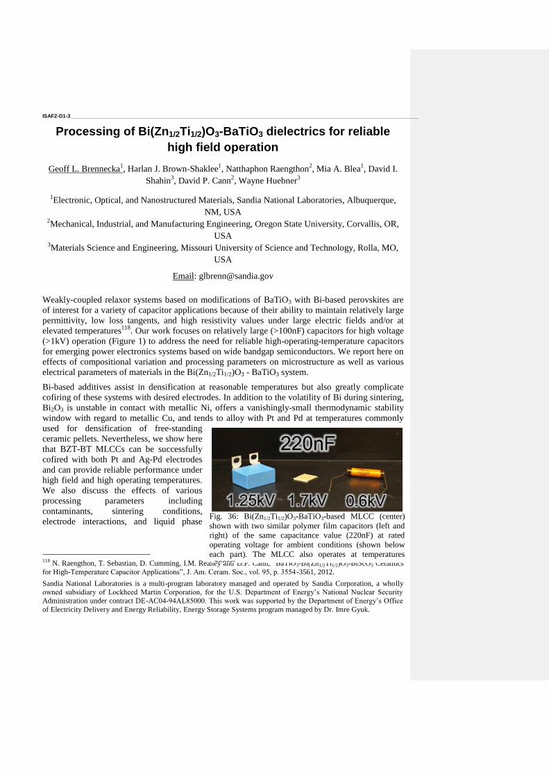
ISAF2-D1-3 _____________________________________________________________________________________________________________________
Processing of Bi(Zn1/2Ti1/2)O3-BaTiO3 dielectrics for reliable
high field operation
Geoff L. Brennecka1, Harlan J. Brown-Shaklee
1, Natthaphon Raengthon
2, Mia A. Blea
1, David I.
Shahin3, David P. Cann
2, Wayne Huebner
3
1Electronic, Optical, and Nanostructured Materials, Sandia National Laboratories, Albuquerque,
NM, USA 2Mechanical, Industrial, and Manufacturing Engineering, Oregon State University, Corvallis, OR,
USA 3Materials Science and Engineering, Missouri University of Science and Technology, Rolla, MO,
USA
Email: [email protected]
Weakly-coupled relaxor systems based on modifications of BaTiO3 with Bi-based perovskites are
of interest for a variety of capacitor applications because of their ability to maintain relatively large
permittivity, low loss tangents, and high resistivity values under large electric fields and/or at
elevated temperatures118
. Our work focuses on relatively large (>100nF) capacitors for high voltage
(>1kV) operation (Figure 1) to address the need for reliable high-operating-temperature capacitors
for emerging power electronics systems based on wide bandgap semiconductors. We report here on
effects of compositional variation and processing parameters on microstructure as well as various
electrical parameters of materials in the Bi(Zn1/2Ti1/2)O3 - BaTiO3 system.
Bi-based additives assist in densification at reasonable temperatures but also greatly complicate
cofiring of these systems with desired electrodes. In addition to the volatility of Bi during sintering,
Bi2O3 is unstable in contact with metallic Ni, offers a vanishingly-small thermodynamic stability
window with regard to metallic Cu, and tends to alloy with Pt and Pd at temperatures commonly
used for densification of free-standing
ceramic pellets. Nevertheless, we show here
that BZT-BT MLCCs can be successfully
cofired with both Pt and Ag-Pd electrodes
and can provide reliable performance under
high field and high operating temperatures.
We also discuss the effects of various
processing parameters including
contaminants, sintering conditions,
electrode interactions, and liquid phase
118
N. Raengthon, T. Sebastian, D. Cumming, I.M. Reaney and D.P. Cann, “BaTiO3-Bi(Zn1/2Ti1/2)O3-BiScO3 Ceramics
for High-Temperature Capacitor Applications”, J. Am. Ceram. Soc., vol. 95, p. 3554-3561, 2012.
Sandia National Laboratories is a multi-program laboratory managed and operated by Sandia Corporation, a wholly
owned subsidiary of Lockheed Martin Corporation, for the U.S. Department of Energy’s National Nuclear Security
Administration under contract DE-AC04-94AL85000. This work was supported by the Department of Energy’s Office
of Electricity Delivery and Energy Reliability, Energy Storage Systems program managed by Dr. Imre Gyuk.
Fig. 36: Bi(Zn1/2Ti1/2)O3-BaTiO3-based MLCC (center)
shown with two similar polymer film capacitors (left and
right) of the same capacitance value (220nF) at rated
operating voltage for ambient conditions (shown below
each part). The MLCC also operates at temperatures
>200°C

additives, on permittivity, resistivity and degradation mechanisms.
ISAF2-D1-4 _____________________________________________________________________________________________________________________
Electromechanical Properties of Hard
Lead-free Bi0.5Na0.5TiO3-based Ceramics
E. Taghaddos, M. Hejazi, and A. Safari
Glenn Howatt Electroceramics Laboratory
Department of Materials Science and Engineering, Rutgers University
607 Taylor Rd, Piscataway, NJ 08854
It has been previously shown that in a ternary system of x[Bi0.5Na0.5TiO3]-y[Bi0.5K0.5TiO3]-(1-x-y)
[Bi0.5Li0.5TiO3], the highest mechanical quality factor (Qm) is obtained at a composition with x and
y values of 0.88 and 0.08, respectively. In this work, processing and electrocmechanical properties
of Mn-doped 0.88[Bi0.5Na0.5TiO3]-0.08[Bi0.5K0.5TiO3]-0.04[Bi0.5Li0.5TiO3] ceramics prepared by
mixed oxide route have been comprehensively studied. Different amount of Mn (0.01, 0.014,
0.015, 0.01625, 0.0175, 0.02, and 0.022) was added to the ceramics either in form of a dopant (B-
site substitution) or as an additive after calcination. Pressed samples were sintered at different
temperatures (1075-1150 oC) and time. It was found that Mn-addition did not exhibit any hardening
effect and in fact led to an increase in the dielectric loss. On the other hand, Qm was remarkably
increased by Mn-doping in the B-site. Mn-doping was also resulted in decreasing in planar coupling
coefficient, dielectric constant, and dielectric loss which are common effects in hard ferroelectrics
doped with an acceptor. The Qm, d33, kp, εr and tanδ values for 0.015 Mn doped sample were 950,
85 pC/N, 0.218, 310, and 0.009, respectively. Sintering temperature in Mn doped BNKLT
ceramics were slightly lower than undoped samples..
ISAF2-D1-5 _____________________________________________________________________________________________________________________
Poling below Coercive Field for Large Piezoelectricity
Xiaoli Tan, Hanzheng Guo, Cheng Ma, Xiaoming Liu
Department of Materials Science and Engineering, Iowa State University, Ames, Iowa/USA
Email: [email protected]
Piezoelectric materials are key to many important technologies, including energy harvesting, noise
cancellation, and minimally invasive surgery. The dominant piezoelectric materials in industry are
polycrystalline ferroelectrics, which must be poled by electric fields to exhibit piezoelectricity.
During electrical poling, the originally randomly oriented polarizations are aligned by the poling
field, forming the macroscopic non-centrosymmetry that is required for piezoelectricity. Therefore,
it is commonly believed that poling fields have to be much greater than the coercive field EC, which
characterizes the difficulty of polarization reversal in ferroelectrics. Such an empirical rule is based
on and supported by numerous experimental observations on all the widely studied piezoelectrics so
far. Poling fields below or around EC only yield very small piezoelectric coefficient d33 values that
are close to zero.
In the present work, we report that well-developed piezoelectric properties are measured in certain
lead-free (1-x)(Bi1/2Na1/2)TiO3–xBaTiO3 compositions even when they are poled at fields
significantly below their measured coercive fields. Prior to poling, these compositions are in the
morphotropic phase boundary region and display a relaxor behavior with the ferrielectric P4bm
structure. Electric field in-situ transmission electron microscopy experiments reveal that this
unusual behavior is originated from the poling of the non-ergodic relaxor ferrielectric phase where
P4bm nanodomains irreversibly coalesce and form extremely thin lamellar domains. Similar
behavior is also confirmed in a lead-containing relaxor ferroelectric (Pb0.92La0.08)(Zr0.65Ti0.35)O3.

Domain engineering
CLUB B
Tuesday, July 23 2013, 10:30 am - 12:00 pm
Chair: To Be Announced
ISAF1-D2-1 _____________________________________________________________________________________________________________________
Investigation of intrinsic domains in PbTiO3 ultrathin films: from nanodots to nanostripes
Céline Lichtensteiger, Pavlo Zubko and Jean-Marc Triscone
DPMC – University of Geneva, 24 Quai Ernest Ansermet, CH – 1211 Genève 4
Email: [email protected]
In ferroelectric ultrathin films, the depolarization field arising from bound charges on the surface of
the film and at the interface with the substrate can be partially screened by free charges from
metallic electrodes, ions from the atmosphere, or mobile charges from within the semiconducting
ferroelectric itself. Even in structurally perfect metallic electrodes, the screening charges will spread
over a small but finite length, giving rise to a nonzero effective screening length that will
dramatically alter the properties of an ultrathin film. In the absence of sufficient free charges, a
ferroelectric has several other ways of minimizing its energy while preserving its polar state, e.g.,
by forming domains of opposite polarization, or rotating the polarization into the plane of the thin
ferroelectric slab 119
.
Using piezo-force microscopy (PFM), we investigate the intrinsic nanodomain structure of PbTiO3
ultrathin films at room temperature.
By changing the degree of screening, the domain structure can be modified or even suppressed in
favour of a uniform monodomain state. Focusing on the effect of film thickness, we observe the evolution of the size and shape of the domains from
large nanodots to small stripes as the PbTiO3 films thickness decreases.
119
Ferroelectricity in ultrathin-film capacitors, C. Lichtensteiger et al, Ch. 12 in Oxide Ultrathin Films, Science and
Technology, Wiley (2011) (arXiv:1208.5309v1 [cond-mat.mtrl-sci])
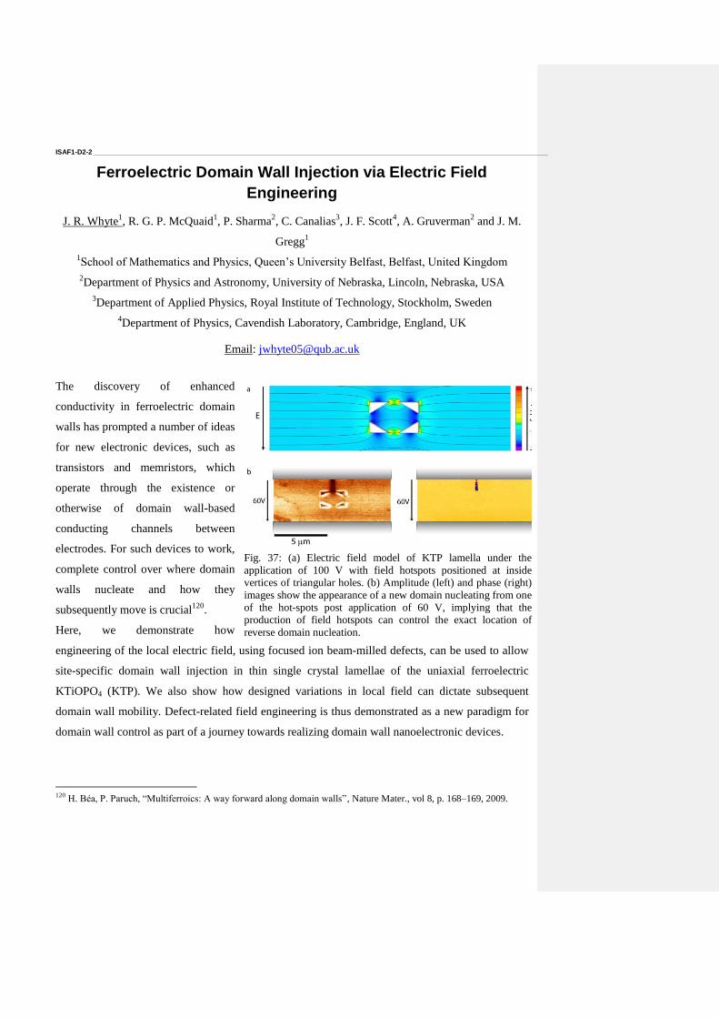
ISAF1-D2-2 _____________________________________________________________________________________________________________________
Ferroelectric Domain Wall Injection via Electric Field
Engineering
J. R. Whyte1, R. G. P. McQuaid
1, P. Sharma
2, C. Canalias
3, J. F. Scott
4, A. Gruverman
2 and J. M.
Gregg1
1School of Mathematics and Physics, Queen’s University Belfast, Belfast, United Kingdom
2Department of Physics and Astronomy, University of Nebraska, Lincoln, Nebraska, USA
3Department of Applied Physics, Royal Institute of Technology, Stockholm, Sweden
4Department of Physics, Cavendish Laboratory, Cambridge, England, UK
Email: [email protected]
The discovery of enhanced
conductivity in ferroelectric domain
walls has prompted a number of ideas
for new electronic devices, such as
transistors and memristors, which
operate through the existence or
otherwise of domain wall-based
conducting channels between
electrodes. For such devices to work,
complete control over where domain
walls nucleate and how they
subsequently move is crucial120
.
Here, we demonstrate how
engineering of the local electric field, using focused ion beam-milled defects, can be used to allow
site-specific domain wall injection in thin single crystal lamellae of the uniaxial ferroelectric
KTiOPO4 (KTP). We also show how designed variations in local field can dictate subsequent
domain wall mobility. Defect-related field engineering is thus demonstrated as a new paradigm for
domain wall control as part of a journey towards realizing domain wall nanoelectronic devices.
120
H. Béa, P. Paruch, “Multiferroics: A way forward along domain walls”, Nature Mater., vol 8, p. 168–169, 2009.
Fig. 37: (a) Electric field model of KTP lamella under the
application of 100 V with field hotspots positioned at inside
vertices of triangular holes. (b) Amplitude (left) and phase (right)
images show the appearance of a new domain nucleating from one
of the hot-spots post application of 60 V, implying that the
production of field hotspots can control the exact location of
reverse domain nucleation.
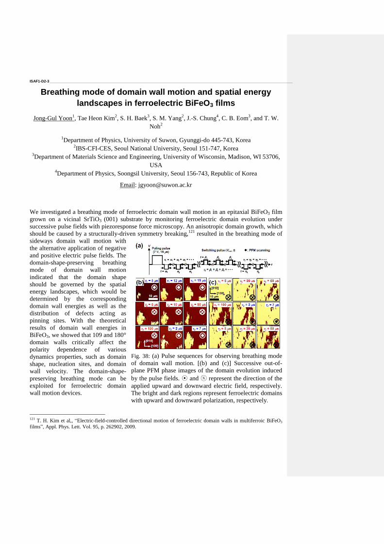
ISAF1-D2-3 _____________________________________________________________________________________________________________________
Breathing mode of domain wall motion and spatial energy
landscapes in ferroelectric BiFeO3 films
Jong-Gul Yoon1, Tae Heon Kim
2, S. H. Baek
3, S. M. Yang
2, J.-S. Chung
4, C. B. Eom
3, and T. W.
Noh2
1Department of Physics, University of Suwon, Gyunggi-do 445-743, Korea
2IBS-CFI-CES, Seoul National University, Seoul 151-747, Korea
3Department of Materials Science and Engineering, University of Wisconsin, Madison, WI 53706,
USA 4Department of Physics, Soongsil University, Seoul 156-743, Republic of Korea
Email: [email protected]
We investigated a breathing mode of ferroelectric domain wall motion in an epitaxial BiFeO3 film
grown on a vicinal SrTiO3 (001) substrate by monitoring ferroelectric domain evolution under
successive pulse fields with piezoresponse force microscopy. An anisotropic domain growth, which
should be caused by a structurally-driven symmetry breaking,121
resulted in the breathing mode of
sideways domain wall motion with
the alternative application of negative
and positive electric pulse fields. The
domain-shape-preserving breathing
mode of domain wall motion
indicated that the domain shape
should be governed by the spatial
energy landscapes, which would be
determined by the corresponding
domain wall energies as well as the
distribution of defects acting as
pinning sites. With the theoretical
results of domain wall energies in
BiFeO3, we showed that 109 and 180°
domain walls critically affect the
polarity dependence of various
dynamics properties, such as domain
shape, nucleation sites, and domain
wall velocity. The domain-shape-
preserving breathing mode can be
exploited for ferroelectric domain
wall motion devices.
121
T. H. Kim et al,, “Electric-field-controlled directional motion of ferroelectric domain walls in multiferroic BiFeO3
films”, Appl. Phys. Lett. Vol. 95, p. 262902, 2009.
Fig. 38: (a) Pulse sequences for observing breathing mode
of domain wall motion. [(b) and (c)] Successive out-of-
plane PFM phase images of the domain evolution induced
by the pulse fields. ⊙ and ⓧ represent the direction of the
applied upward and downward electric field, respectively.
The bright and dark regions represent ferroelectric domains
with upward and downward polarization, respectively.

ISAF1-D2-4 _____________________________________________________________________________________________________________________
Multiscaling analysis and thermal quench effects of domain
walls in epitaxial BiFeO3 thin films
Benedikt Ziegler1, Ingrid Infante
2, Stephane Fusil
2, Manuel Bibes
2 and Patrycja Paruch
1
1MaNEP-DPMC, University of Geneva, Geneva, Switzerland
2Unité Mixte de Physique CNRS/Thales, Palaiseau Cedex, France
Email: [email protected]
The coexistence of ferroelectric and antiferromagnetic ordering at room temperature have led to
intense research on multiferroic BiFeO3. In addition, the recent discoveries of interesting new
phenomena like conducting ferroelectric domain walls122
make it a promising candidate for
nanoelectronic applications123
.
Here, we present our study of the microscopic behavior of such domain walls within the broader
framework of elastic disordered systems, using vertical and lateral piezoresponse force microscopy
to study the roughness of artificially written and intrinsic domain walls in ambient conditions and
under thermal cycling. A multiscaling analysis of the domain walls can be used to discriminate
between different kinds of disorder. While this analysis was previously applied to artificially written
ferroelectric domain walls124
, we use it here to study intrinsic stripe-like 71° multiferroic domain
walls, which are potentially better equilibrated and have a richer internal structure due to strain and
potentially also electromagnetic coupling. From these studies we extract a characteristic length
scale, below which the domain walls show a mono-affine scaling, usually an indication of weak
collective pinning in random disorder. However, unlike for the individual artificially written walls,
in this case long-range interactions between the domain walls appear to dominate the effective
elastic behavior. The domain walls show higher roughening than purely artificially written
ferroelectric domain walls. Independently, we also present the evolution of domain wall roughness
with thermal cycling125
in artificially written walls in BiFeO3.
122
Seidel, J., et al., Nature Mater. 8, 229, 2009 123
Catalan, G., et al., Rev. Mod. Phys. 84, 119-156, 2012 124
Guyonnet, J., et al., Phys. Rev. Lett. 109, 147601, 2012 125
Paruch, P., et al., Phys. Rev. B 85, 214115, 2012
ISAF1-D2-5 _____________________________________________________________________________________________________________________
Nanodomain Structuring of Uniaxial Ferroelectrics.
Achievements in Nanodomain Engineering
Shur Vladimir 1,2
1Ferroelectric Laboratory, Ural Federal University, Ekaterinburg, Russia
2Labfer Ltd., Ekaterinburg, Russia
Email: [email protected]
Nanodomain engineering is the important modern target of the ferroelectric science and technology.
The production of ferroelectric crystals with periodical tailored stable domain structure used for
spatial modulation of their electro-optic, nonlinear optical and piezoelectric properties allow to
manufacture various devices with upgraded performance. The fabrication of sub-micron-pitch
quasi-regular domain gratings and engineered structures with nanoscale precision for photonic
applications needs the deeper research of domain formation with submicron spatial resolution.
The set of modern high-resolution methods including piezoresponse force microscopy, scanning
electron microscopy and confocal Raman microscopy applied for domain study in nanoscale has
allowed to reveal the important role of nanodomain kinetics and to investigate the evolution of self-
assembled nanodomain structures. The resent important achievements in studying of the
nanodomain structure evolution obtained in highly non-equilibrium switching conditions realized
by various methods and characterized by ineffective screening of depolarization fields has been
reviewed. Several new effects leading to formation of the quasi-regular dendrite nanodomain
structures has been demonstrated.
The crystals of lithium niobate and lithium tantalate family were studied both as the model
ferroelectrics and as the most important for application nonlinear optical materials. Their simple
domain structure and ability to change the bulk screening rate in wide range by heating allows to
realize the nanodomain structuring.
The nanodomain kinetics has been studied in the samples with the surface layer modified by proton
exchange and during switching by pyroelectric field during cooling after multiply pulse laser
heating. The types of nanoscale domain structures and original scenarios of their evolutions have
been singled out. The unique information about evolution of the nanodomain structures has been
revealed by analysis of the domain images at different depth in the bulk obtained by scanning laser
confocal Raman microscopy. The stable self-assembled stripe domain structures with periods about
20 nm has been produced.
The obtained knowledge opens the new approach to the nanodomain engineering. The high-
efficient crystals for laser light frequency conversion in spectral range from 0.4 to 4 m have been
manufactured.
The equipment of the UCSU “Modern Nanotechnology”, Institute of Natural Sciences, UrFU has
been used. The research was made possible in part by RFBR (Grants 13-02-01391-а, 12-02-31377,
11-02-91066-CNRS-а), by Ministry of Education and Science (Сontract 14.513.12.0006).

High Temperature Piezoelectrics
CLUB C
Tuesday, July 23 2013, 10:30 am - 12:00 pm
Chair: David Cann
Oregon State University
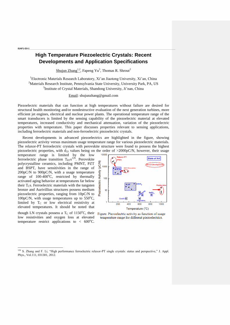
ISAF1-D3-1 _____________________________________________________________________________________________________________________
High Temperature Piezoelectric Crystals: Recent
Developments and Application Specifications
Shujun Zhang1,2
, Fapeng Yu3, Thomas R. Shrout
2
1Electronic Materials Research Laboratory, Xi’an Jiaotong University, Xi’an, China
2Materials Research Institute, Pennsylvania State University, University Park, PA, US
3Institute of Crystal Materials, Shandong University, Ji’nan, China
Email: [email protected]
Piezoelectric materials that can function at high temperatures without failure are desired for
structural health monitoring and/or nondestructive evaluation of the next generation turbines, more
efficient jet engines, electrical and nuclear power plants. The operational temperature range of the
smart transducers is limited by the sensing capability of the piezoelectric material at elevated
temperatures, increased conductivity and mechanical attenuation, variation of the piezoelectric
properties with temperature. This paper discusses properties relevant to sensing applications,
including ferroelectric materials and non-ferroelectric piezoelectric crystals.
Recent developments in advanced piezoelectrics are highlighted in the figure, showing
piezoelectric activity versus maximum usage temperature range for various piezoelectric materials.
The relaxor-PT ferroelectric crystals with perovskite structure were found to possess the highest
piezoelectric properties, with d33 values being on the order of >2000pC/N, however, their usage
temperature range is limited by the low
ferroelectric phase transition TRTs126
. Perovskite
polycrystalline ceramics, including PMNT, PZT
and BSPT, have sensitivities in the range of
200pC/N to 900pC/N, with a usage temperature
range of 100-400oC, restricted by thermally
activated aging behavior at temperatures far below
their TCs. Ferroelectric materials with the tungsten
bronze and Aurivillius structures possess medium
piezoelectric properties, ranging from 10pC/N to
100pC/N, with usage temperatures up to 550oC,
limited by TC or low electrical resistivity at
elevated temperatures. It should be noted that
though LN crystals possess a TC of 1150oC, their
low resistivities and oxygen loss at elevated
temperature restrict applications to < 600oC.
126
S. Zhang and F. Li, “High performance ferroelectric relaxor-PT single crystals: status and perspective,” J. Appl.
Phys., Vol.111, 031301, 2012.
Generally, nonferroelectric piezoelectric single crystals possess low sensitivity, falling in the range
of 1-20pC/N, however, their ultralow mechanical and dielectric losses, and high electrical
resistivities, make them ideal candidates for ultra-high temperature sensing applications127
.
127
S. Zhang and F. Yu, “Piezoelectric materials for high temperature sensors,” J. Am. Ceram. Soc., Vol.94, pp.3153-
3170, 2011.
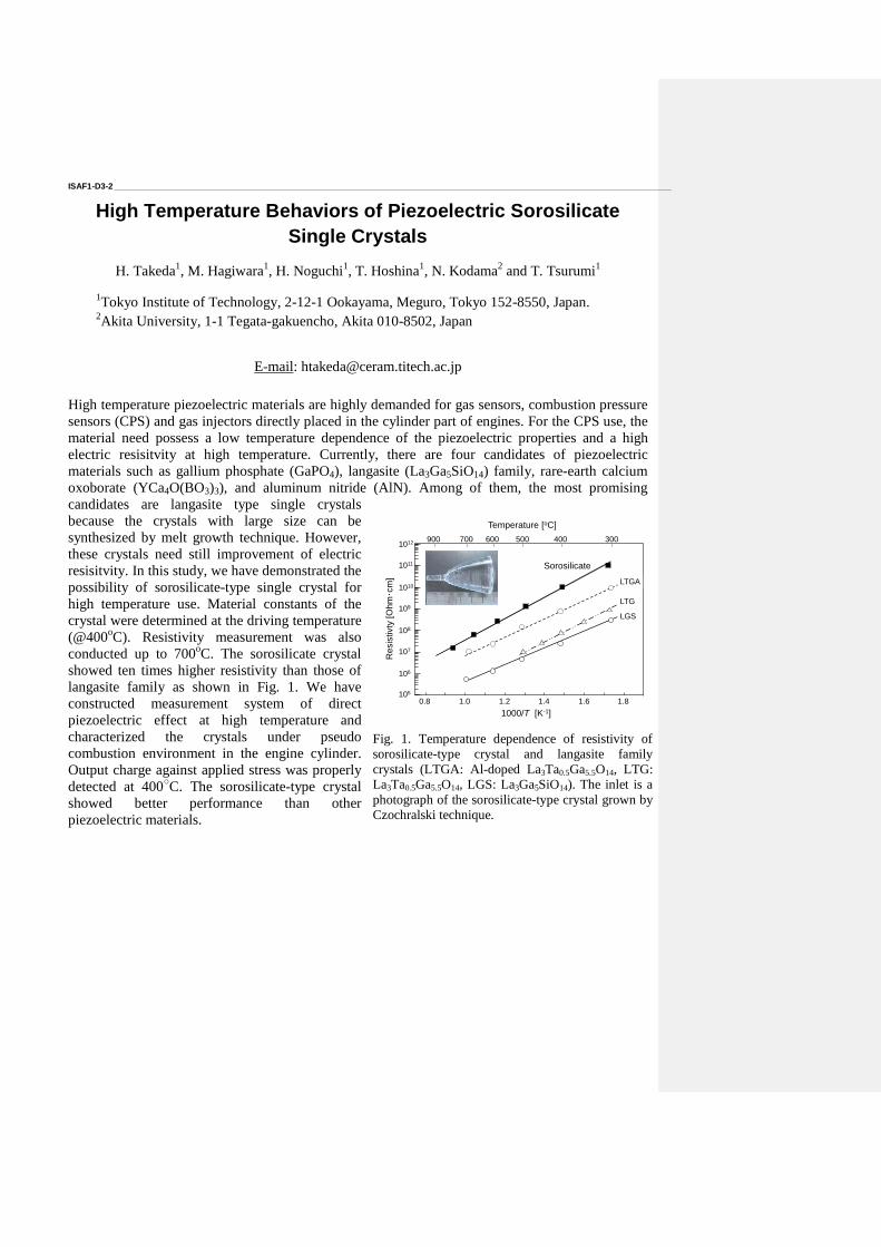
ISAF1-D3-2 _____________________________________________________________________________________________________________________
High Temperature Behaviors of Piezoelectric Sorosilicate
Single Crystals
H. Takeda1, M. Hagiwara
1, H. Noguchi
1, T. Hoshina
1, N. Kodama
2 and T. Tsurumi
1
1Tokyo Institute of Technology, 2-12-1 Ookayama, Meguro, Tokyo 152-8550, Japan.
2Akita University, 1-1 Tegata-gakuencho, Akita 010-8502, Japan
E-mail: [email protected]
High temperature piezoelectric materials are highly demanded for gas sensors, combustion pressure
sensors (CPS) and gas injectors directly placed in the cylinder part of engines. For the CPS use, the
material need possess a low temperature dependence of the piezoelectric properties and a high
electric resisitvity at high temperature. Currently, there are four candidates of piezoelectric
materials such as gallium phosphate (GaPO4), langasite (La3Ga5SiO14) family, rare-earth calcium
oxoborate (YCa4O(BO3)3), and aluminum nitride (AlN). Among of them, the most promising
candidates are langasite type single crystals
because the crystals with large size can be
synthesized by melt growth technique. However,
these crystals need still improvement of electric
resisitvity. In this study, we have demonstrated the
possibility of sorosilicate-type single crystal for
high temperature use. Material constants of the
crystal were determined at the driving temperature
(@400oC). Resistivity measurement was also
conducted up to 700oC. The sorosilicate crystal
showed ten times higher resistivity than those of
langasite family as shown in Fig. 1. We have
constructed measurement system of direct
piezoelectric effect at high temperature and
characterized the crystals under pseudo
combustion environment in the engine cylinder.
Output charge against applied stress was properly
detected at 400○C. The sorosilicate-type crystal
showed better performance than other
piezoelectric materials.
105
106
107
108
109
1010
1011
1012
1.0 1.2 1.4 1.6 1.8
300400500600
Temperature [oC]
1000/T [K-1]
Re
sis
tivty
[Oh
m・c
m]
0.8
700900
LTG
LGS
LTGA
YCa4O(BO3)3
Sorosilicate
Fig. 1. Temperature dependence of resistivity of
sorosilicate-type crystal and langasite family
crystals (LTGA: Al-doped La3Ta0.5Ga5.5O14, LTG:
La3Ta0.5Ga5.5O14, LGS: La3Ga5SiO14). The inlet is a
photograph of the sorosilicate-type crystal grown by
Czochralski technique.
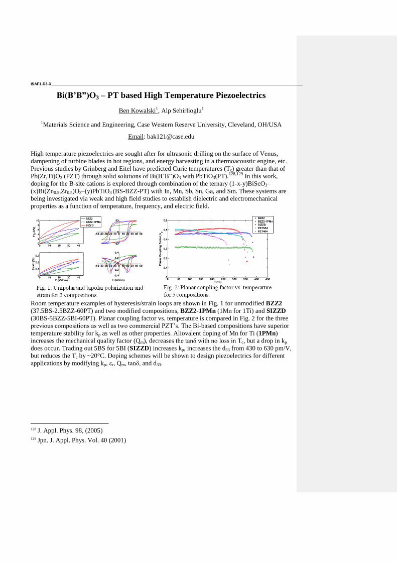
ISAF1-D3-3 _____________________________________________________________________________________________________________________
Bi(B’B”)O3 – PT based High Temperature Piezoelectrics
Ben Kowalski1, Alp Sehirlioglu
1
1Materials Science and Engineering, Case Western Reserve University, Cleveland, OH/USA
Email: [email protected]
High temperature piezoelectrics are sought after for ultrasonic drilling on the surface of Venus,
dampening of turbine blades in hot regions, and energy harvesting in a thermoacoustic engine, etc.
Previous studies by Grinberg and Eitel have predicted Curie temperatures (Tc) greater than that of
Pb(Zr,Ti)O3 (PZT) through solid solutions of Bi(B’B”)O3 with PbTiO3(PT).128,129
In this work,
doping for the B-site cations is explored through combination of the ternary (1-x-y)BiScO3–
(x)Bi(Zn0.5,Zr0.5)O3–(y)PbTiO3 (BS-BZZ-PT) with In, Mn, Sb, Sn, Ga, and Sm. These systems are
being investigated via weak and high field studies to establish dielectric and electromechanical
properties as a function of temperature, frequency, and electric field.
Room temperature examples of hysteresis/strain loops are shown in Fig. 1 for unmodified BZZ2
(37.5BS-2.5BZZ-60PT) and two modified compositions, BZZ2-1PMn (1Mn for 1Ti) and SIZZD
(30BS-5BZZ-5BI-60PT). Planar coupling factor vs. temperature is compared in Fig. 2 for the three
previous compositions as well as two commercial PZT’s. The Bi-based compositions have superior
temperature stability for kp as well as other properties. Aliovalent doping of Mn for Ti (1PMn)
increases the mechanical quality factor (Qm), decreases the tanδ with no loss in Tc, but a drop in kp
does occur. Trading out 5BS for 5BI (SIZZD) increases kp, increases the d33 from 430 to 630 pm/V,
but reduces the Tc by ~20°C. Doping schemes will be shown to design piezoelectrics for different
applications by modifying kp, εr, Qm, tanδ, and d33.
128
J. Appl. Phys. 98, (2005) 129
Jpn. J. Appl. Phys. Vol. 40 (2001)
ISAF1-D3-4 _____________________________________________________________________________________________________________________
Pb(Yb1/2Nb1/2)O3-PbTiO3, structure-property relation in a high
temperature piezoelectric material
Charlotte Cochard1,2
, Christine Bogicevic1, Xavier Bril
1, Nicolas Guiblin
1, Florence
Porcher3,Orland Guedes
2, Pierre-Eymeric Janolin
1
1 Laboratoire SPMS , UMR CNRS-École Centrale Paris, Châtenay-Malabry, France
2 Schlumberger, Clamart, France
3Laboratoire LLB, CEA, Saclay, France
Email: [email protected]
Piezoelectricity has attracted a considerable amount of work due to the variety of possible
applications such as accelerometers, gyroscopes or transducers. Solid solutions of relaxors and
classical ferroelectrics are know to exhibit enhanced piezoelectric properties close to the
morphotropic phase boundary (MPB) compared to the pure materials counterpart. Therefore,
materials such as Pb(Mg1/3Nb2/3)O3-PbTiO3 or Pb(Zn1/3Nb2/3)O3-PbTiO3 have been extensively
studied over the last 50 years. On the contrary, Pb(Yb1/2Nb1/2)O3-PbTiO3 (PYN-PT) which is long
known to have good piezoelectric properties (d33=510pC/N) and a relatively high Curie temperature
(~370°C at the MPB) has not been examined so extensively probably because of the scarcity of
single crystals
In this work, we will present experimental data obtained on PYN-PT of different compositions
close to the MPB. These data were obtained by X-ray diffraction, neutron scattering as well as
dielectric and piezoelectric measurement as a function of temperature, enabling a clearer picture of
the structure-property relation around the MPB to emerge in this material of crucial importance for
high-temperature applications.
ISAF1-D3-5 _____________________________________________________________________________________________________________________
Piezoceramic Materials for High-Temperature & High-Pressure
Applications in Oilfield Exploration & Production
Kenneth Liang1, Wanda Wolny
2, Dragan Damjanovic
3, Torsten Bove
2
1Schlumberger-Doll Research, Cambridge, MA, USA
2Meggitt A/S, Kvistgaard, Denmark
3Institute of Materials, EFPL, Lausanne, Switzerland
Email: [email protected]
Ultrasonic measurements play important roles in many oilfield services applications. With oil wells
reaching ever increasing depths, the operating environment is characterized by high temperature
and high pressure (175˚C, 20,000psi and beyond). Ultrasonic transducers typically operate into a
liquid-filled borehole. Lead metaniobate, mainly due to its low acoustic impedance and despite its
low kt, is used where both efficiency and bandwidth are required. There is ongoing effort though to
seek equivalent and better substitute materials. This work is a continuation of a previous study
carried out on Pz31 and Pz36, two PZT-based materials developed by Meggitt A/S with engineered
porosity130
. While these materials are well-behaved with temperature, both tend to depole when
subjected to 15,000psi, with Pz31 being more susceptible to depoling than Pz36. The polarization
can be restored by repoling afterwards, indicating that depoling is due only to rearrangement of
polarization within samples and not mechanical failure. The depoling mechanism is not understood
and the difference in vulnerability to static pressure appears to be inconsistent with the relative
degree of hardness of, and the rhombohedral and tetragonal structures of Pz31 and Pz36
respectively. To develop insight, we carried out identical temperature and pressure tests on the
fully densified versions of Pz31 and Pz36, Pz24 and Pz26 respectively. The experimental setup is
described and the results and analyses are given.
A bismuth titanate based material, Pz46, has also been studied for its suitability under extreme
conditions. It exhibits kt ~ 0.2, slightly higher acoustic impedance than lead metaniobate, Curie
temperature in excess of 600˚C, and is highly resistant to shock. The material has been temperature
cycled up to 200˚C with no degradation and results of pressure cycling to assess its field worthiness
will be reported and discussed.
130
Bove, Liang, Wolny, “Experimental Study of Temperature & Pressure Effects on High-Porosity PZT Materials,”
IEEE Ultrasonics Symposium Proceedings, Dresden, 2012

Lead-free ceramics: E-field Effects
CLUB A
Tuesday, July 23 2013, 02:00 pm - 03:30 pm
Chair: Xiaoli Tan
Iowa State University
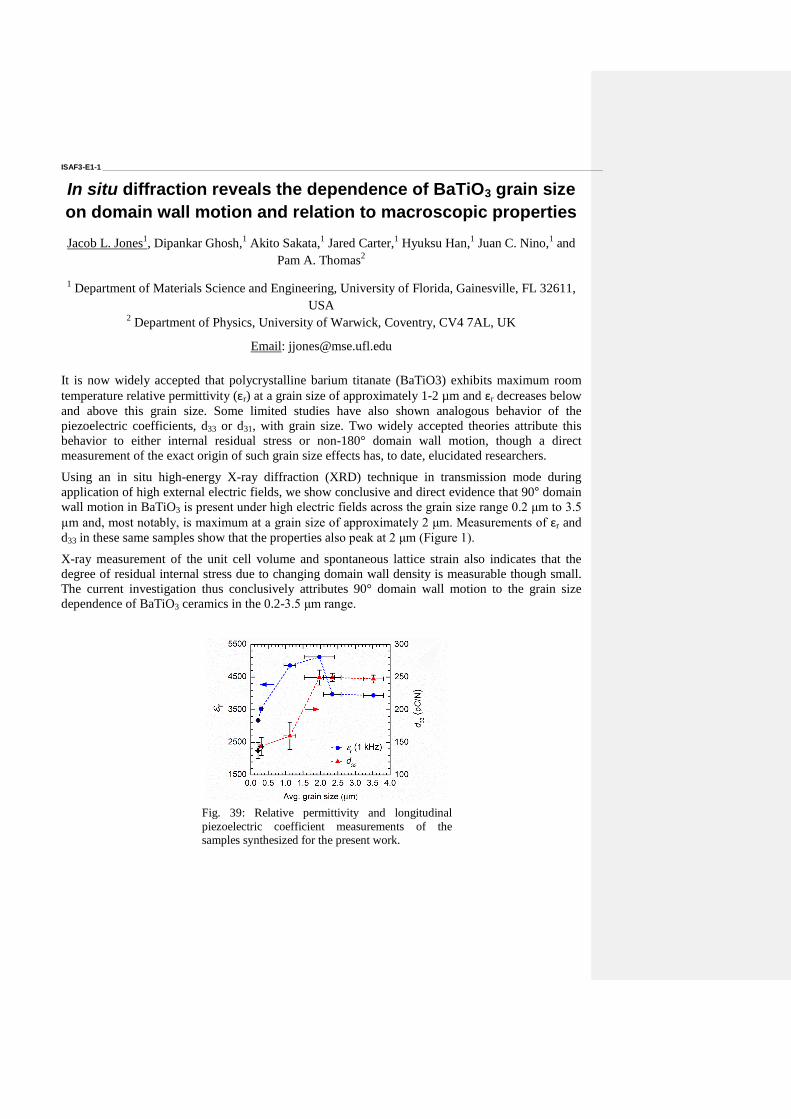
ISAF3-E1-1 _____________________________________________________________________________________________________________________
In situ diffraction reveals the dependence of BaTiO3 grain size
on domain wall motion and relation to macroscopic properties
Jacob L. Jones1, Dipankar Ghosh,
1 Akito Sakata,
1 Jared Carter,
1 Hyuksu Han,
1 Juan C. Nino,
1 and
Pam A. Thomas2
1 Department of Materials Science and Engineering, University of Florida, Gainesville, FL 32611,
USA 2 Department of Physics, University of Warwick, Coventry, CV4 7AL, UK
Email: [email protected]
It is now widely accepted that polycrystalline barium titanate (BaTiO3) exhibits maximum room
temperature relative permittivity (εr) at a grain size of approximately 1-2 µm and εr decreases below
and above this grain size. Some limited studies have also shown analogous behavior of the
piezoelectric coefficients, d33 or d31, with grain size. Two widely accepted theories attribute this
behavior to either internal residual stress or non-180° domain wall motion, though a direct
measurement of the exact origin of such grain size effects has, to date, elucidated researchers.
Using an in situ high-energy X-ray diffraction (XRD) technique in transmission mode during
application of high external electric fields, we show conclusive and direct evidence that 90° domain
wall motion in BaTiO3 is present under high electric fields across the grain size range 0.2 μm to 3.5
µm and, most notably, is maximum at a grain size of approximately 2 μm. Measurements of εr and
d33 in these same samples show that the properties also peak at 2 μm (Figure 1).
X-ray measurement of the unit cell volume and spontaneous lattice strain also indicates that the
degree of residual internal stress due to changing domain wall density is measurable though small.
The current investigation thus conclusively attributes 90° domain wall motion to the grain size
dependence of BaTiO3 ceramics in the 0.2-3.5 μm range.
Fig. 39: Relative permittivity and longitudinal
piezoelectric coefficient measurements of the
samples synthesized for the present work.
ISAF3-E1-2 _____________________________________________________________________________________________________________________
High-speed data capture of the electric field induced phase
transition in potassium sodium bismuth titanate
Tim P. Comyn1, Andrew J. Bell
1, Annette Kleppe
2
1Institute for Materials Research, University of Leeds, Leeds, UK
2Diamond Light Source, Harwell Science Campus, Didcot, Oxfordshire, UK
Email: [email protected]
The lead free system KNBT (xK1/2Bi1/2TiO3-(1-x)Na1/2Bi1/2TiO3) exhibits an electric field induced
phase transition from rhombohedral to mixed phase rhombohedral and tetragonal, for x=0.2, as
confirmed using in-situ synchrotron experiments. Here, we track the phase transition at high speed,
using a state of the art Pilatus x-ray detector. Strobing has been used by other groups to track
ferroelectric materials driven around major and minor hysteresis loops, using synchrotron and
neutron radiation, but such techniques are not appropriate here. The phase transition which occurs
in KNBT during poling is irreversible, except by heating to above 400 0C.
Data collected at 100 Hz shows that an electric field induced strain precedes the phase transition.
The detector was synchronized with the electric drive field. The complexities of the experiment, and
further improvements are discussed.
ISAF3-E1-3 _____________________________________________________________________________________________________________________
Effect of Applied Field Direction in {001}pc Oriented
Bi0.5Na0.5TiO3-7BaTiO3-2K0.5Na0.5NbO3 Bulk Ceramics
aChris M. Fancher,
aJohn E. Blendell, and
a,bKeith J. Bowman
b) Mechanical, Materials & Aerospace Engineering, Illinois Institute of
Technology, Chicago, Illinois 60616, USA
The high strain response of the Bi0.5Na0.5TiO3-yBaTiO3-xK0.5Na0.5NbO3 system has been attributed
to a reversible electric-field-induced phase transformation from a pseudocubic to a distorted polar
structure. A recent in situ experiment has reported BNT-6BT-2KNN to transform from an
undistorted tetragonal into a phase mixture of distorted rhombohedral and tetragonal phases. In this
work, the effect that crystallographic texture and texture symmetry have on the field-induced phase
transformation of BNT-7BT-2KNN bulk ceramics was investigated. Bulk BNT-7BT-2KNN
ceramics with a 8.6 multiples of a random distribution (MRD) {001}pc fiber texture were prepared
using the tape-casting method with a 5wt% template fraction. Texturing improved the high field
strain response of BNT-7BT-2KNN by 47%. To understand the origin of this improvement, the
effect texture symmetry has on the strain response was investigated by applying an electric field
parallel or perpendicular to the {001}pc fiber texture axis. Applying the electric field perpendicular
to the fiber axis resulted in a high field strain response that was 16% lower compared to the strain
response for a field applied along the fiber axis. Field direction did not affect the volume expansion
during electric cycling; suggesting the field-induced phase transformation is independent of the
applied field direction. In situ diffraction showed that field direction does not effect the induced
phase formation; however, field direction did affect the ferroelastic texture and electric field
required to induce the polar phase.
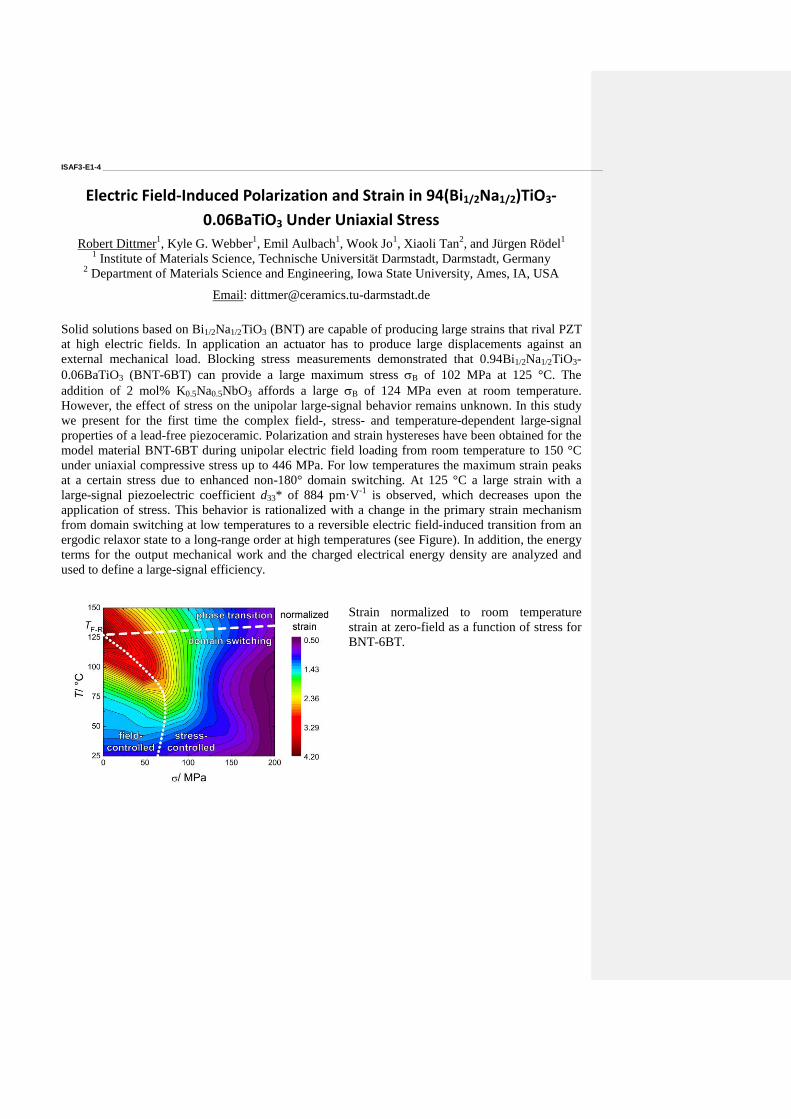
ISAF3-E1-4 _____________________________________________________________________________________________________________________
Electric Field-Induced Polarization and Strain in 94(Bi1/2Na1/2)TiO3-
0.06BaTiO3 Under Uniaxial Stress
Robert Dittmer1, Kyle G. Webber
1, Emil Aulbach
1, Wook Jo
1, Xiaoli Tan
2, and Jürgen Rödel
1
1 Institute of Materials Science, Technische Universität Darmstadt, Darmstadt, Germany
2 Department of Materials Science and Engineering, Iowa State University, Ames, IA, USA
Email: [email protected]
Solid solutions based on Bi1/2Na1/2TiO3 (BNT) are capable of producing large strains that rival PZT
at high electric fields. In application an actuator has to produce large displacements against an
external mechanical load. Blocking stress measurements demonstrated that 0.94Bi1/2Na1/2TiO3-
0.06BaTiO3 (BNT-6BT) can provide a large maximum stress B of 102 MPa at 125 °C. The
addition of 2 mol% K0.5Na0.5NbO3 affords a large B of 124 MPa even at room temperature.
However, the effect of stress on the unipolar large-signal behavior remains unknown. In this study
we present for the first time the complex field-, stress- and temperature-dependent large-signal
properties of a lead-free piezoceramic. Polarization and strain hystereses have been obtained for the
model material BNT-6BT during unipolar electric field loading from room temperature to 150 °C
under uniaxial compressive stress up to 446 MPa. For low temperatures the maximum strain peaks
at a certain stress due to enhanced non-180° domain switching. At 125 °C a large strain with a
large-signal piezoelectric coefficient d33* of 884 pm·V-1
is observed, which decreases upon the
application of stress. This behavior is rationalized with a change in the primary strain mechanism
from domain switching at low temperatures to a reversible electric field-induced transition from an
ergodic relaxor state to a long-range order at high temperatures (see Figure). In addition, the energy
terms for the output mechanical work and the charged electrical energy density are analyzed and
used to define a large-signal efficiency.
Strain normalized to room temperature
strain at zero-field as a function of stress for
BNT-6BT.
ISAF3-E1-5 _____________________________________________________________________________________________________________________
Exploration of Microscopic Mechanisms of the Polarization
Switching in Lead-free BZT-xBCT Ferroelectrics
Sergey Zhukov, Yuri Genenko, Matias Acosta, Heide Humburg, Wook Jo and Heinz von Seggern
1Institut für Materialwissenschaft, TU Darmstadt, Darmstadt, Germany
Email: [email protected]
Nowadays lead-free ferroelectric materials are receiving considerable attention as replacement for
the market dominating, toxic lead-containing PZT ceramics. Recently discovered Ba(Zr0.2Ti 0.8)O3-
x(Ba0.7Ca0.3)TiO3 compositions show piezoelectric properties comparable to that of PZT.131
Similar
to PZT, BZT-xBCT possesses a morphotropic phase boundary (MPB) where piezoelectric
properties peak. At room temperature this boundary is at x = 50% between the rhombohedral BZT
and the tetragonal BCT.
In the current research the polarization switching process in different BZT-xBCT compositions
(0.3 x 0.6) has been studied over a broad time domain covering range from 1μs to 100s. For all
compositions investigated the temporal evolution of the switched polarization exhibits a rather
complex shape which cannot be rationalized by the classical switching concept of nucleation and
grow of reversed domains known also as the Kolmogorov-Avrami-Ishibashi (KAI) model. Unlike
the KAI approach, the recently developed Inhomogeneous Field Mechanism (IFM) model132,133
provides an adequate fit to the experimental results. Moreover, the experimentally obtained
dependencies of the switching time on the electric field strongly suggest the existence of two
distinct switching mechanisms in different field regions. The microscopic origin of both
mechanisms as well as the evolution of their parameters with composition, microstructure and
temperature will be discussed.
131
W.F. Liu, X.B. Ren, “Large Piezoelectric Effect in Pb-Free Ceramics”, Phys. Rev. Lett., 103, 257602, 2009. 132
S. Zhukov, Y. A. Genenko, O. Hirsch, J. Glaum, T. Granzow, H. von Seggern, “Dynamics of polarization reversal in
virgin and fatigued ferroelectric ceramics by inhomogeneous field mechanism”, Phys. Rev. B, 82, 014109, 2010. 133
Y. A. Genenko, S. Zhukov, S.V. Yampolskii, J. Schütrumpf, R. Dittmer, W. Jo, H. Kungl , M.J. Hoffmann, H. von
Seggern, “Universal Polarization Switching Behavior of Disordered Ferroelectrics”, Adv. Funct. Mater., 22, 2058-2066,
2012.
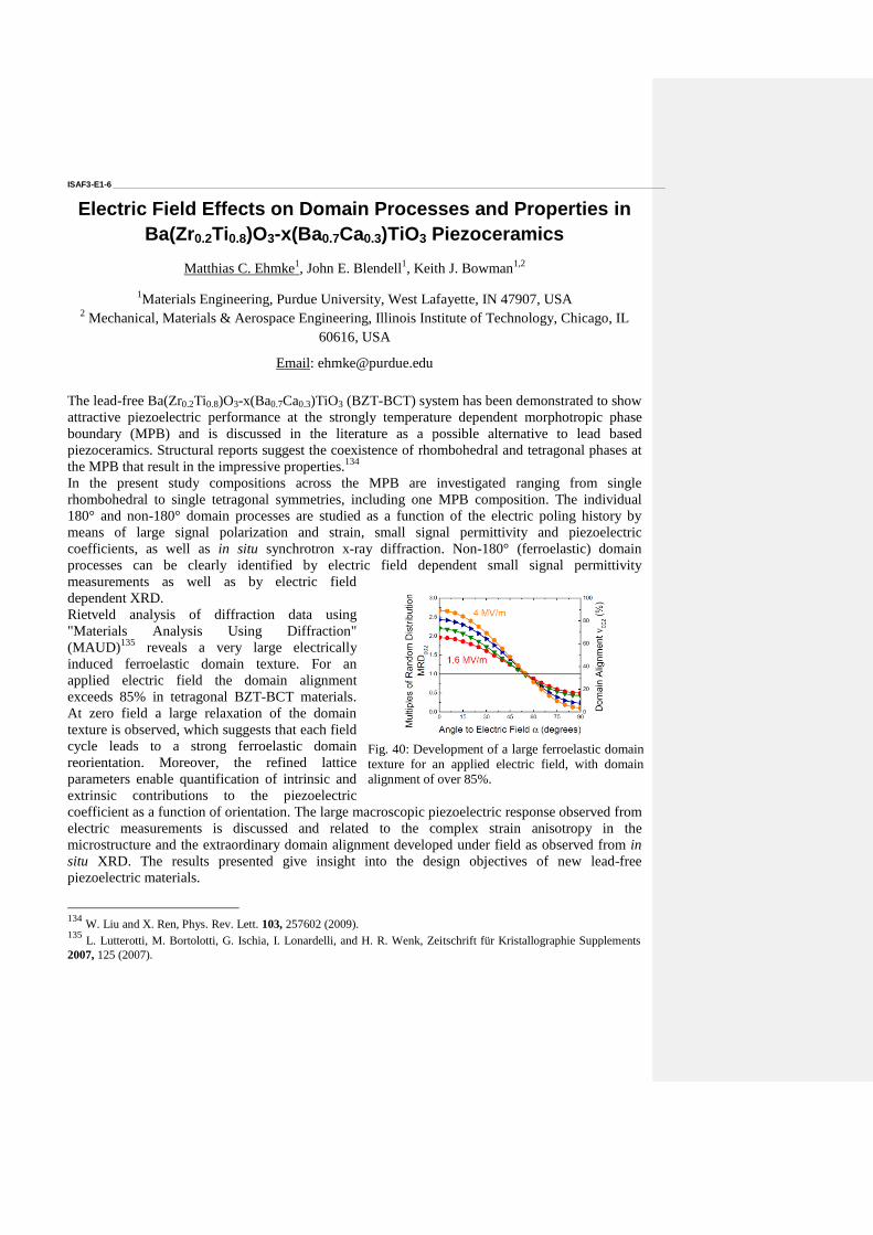
ISAF3-E1-6 _____________________________________________________________________________________________________________________
Electric Field Effects on Domain Processes and Properties in
Ba(Zr0.2Ti0.8)O3-x(Ba0.7Ca0.3)TiO3 Piezoceramics
Matthias C. Ehmke1, John E. Blendell
1, Keith J. Bowman
1,2
1Materials Engineering, Purdue University, West Lafayette, IN 47907, USA
2 Mechanical, Materials & Aerospace Engineering, Illinois Institute of Technology, Chicago, IL
60616, USA
Email: [email protected]
The lead-free Ba(Zr0.2Ti0.8)O3-x(Ba0.7Ca0.3)TiO3 (BZT-BCT) system has been demonstrated to show
attractive piezoelectric performance at the strongly temperature dependent morphotropic phase
boundary (MPB) and is discussed in the literature as a possible alternative to lead based
piezoceramics. Structural reports suggest the coexistence of rhombohedral and tetragonal phases at
the MPB that result in the impressive properties.134
In the present study compositions across the MPB are investigated ranging from single
rhombohedral to single tetragonal symmetries, including one MPB composition. The individual
180° and non-180° domain processes are studied as a function of the electric poling history by
means of large signal polarization and strain, small signal permittivity and piezoelectric
coefficients, as well as in situ synchrotron x-ray diffraction. Non-180° (ferroelastic) domain
processes can be clearly identified by electric field dependent small signal permittivity
measurements as well as by electric field
dependent XRD.
Rietveld analysis of diffraction data using
"Materials Analysis Using Diffraction"
(MAUD)135
reveals a very large electrically
induced ferroelastic domain texture. For an
applied electric field the domain alignment
exceeds 85% in tetragonal BZT-BCT materials.
At zero field a large relaxation of the domain
texture is observed, which suggests that each field
cycle leads to a strong ferroelastic domain
reorientation. Moreover, the refined lattice
parameters enable quantification of intrinsic and
extrinsic contributions to the piezoelectric
coefficient as a function of orientation. The large macroscopic piezoelectric response observed from
electric measurements is discussed and related to the complex strain anisotropy in the
microstructure and the extraordinary domain alignment developed under field as observed from in
situ XRD. The results presented give insight into the design objectives of new lead-free
piezoelectric materials.
134
W. Liu and X. Ren, Phys. Rev. Lett. 103, 257602 (2009). 135
L. Lutterotti, M. Bortolotti, G. Ischia, I. Lonardelli, and H. R. Wenk, Zeitschrift für Kristallographie Supplements
2007, 125 (2007).
Fig. 40: Development of a large ferroelastic domain
texture for an applied electric field, with domain
alignment of over 85%.

Multiferroics
CLUB B
Tuesday, July 23 2013, 02:00 pm - 03:30 pm
Chair: Ruediger-A. Eichel
Forschungszentrum Juelich
ISAF2-E2-1 _____________________________________________________________________________________________________________________
Direct Observation of Electric and Magnetic Field induced Ferroelectric Switching in a Room Temperature Multiferroic
D. M. Evans1*
, M. Arredondo1, A. Schilling
1, Ashok Kumar
2,3, D. Sanchez
2, N. Ortega
2, R. S.
Katiyar2, J. F. Scott
4 and J. M. Gregg
1
1 School of Mathematics and Physics, Queen's University Belfast, Belfast, N. Ireland, BT7 1NN,
UK. 2 Department of Physics and Institute of Multifunctional Materials, University of Puerto Rico, San
Juan, P.R., USA. 3 Materials Physics and Engineering Division, National Physical Laboratory, New Delhi-110012,
India 4 Department of Physics, Cavendish Laboratory, J. J. Thomson Ave., Cambridge, CB3 0HE, UK.
Email: [email protected]
For any material to realize a multiferroic device there must be coupling between the ferromagnetism
and ferroelectricity. This has been shown at low temperature by switching magnetically and
electrically as far back as the 60s [1]. However, it was not until 2006 that any form of coupling was
demonstrated at room temperature [2]. Zhao et al. switched antiferromagnetic domains in BiFeO3
using an electric field. Despite this progress in switching antiferromagnetic domains no one has
directly observed switching, at room temperature, of ferromagnetic domains by using an electric
field, or ferroelectric domains by using a magnetic field.
In this talk, we will show electrical switching in a co-planar geometry, imaged with a PFM, we then
show how a comparable remanent ferroelectric domains pattern can be achieved with a magnetic
field; the authors believe this is the first demonstration of equivalence between electric and
magnetic field at room temperature. TEM is used to investigate the domain hierarchy and to look at
preliminary evidence that coupling occurs on the lowest level of hierarchy, on a scale of order tens
of nanometers. Finally we gain an order of magnitude estimate for the effective magnetoelectric
coupling coefficient[4] and compare it to other values in the literature. All our samples are single
crystal slabs of ca. (PbZr0.53Ti0.47O3)0.6-(PbFe0.5Ta0.5O3)0.4 cut from single grains of bulk
multiferroic ceramics [3] by using a Focused Ion Beam Microscope.
[1] E. Ascher et al., J. Appl. Phys. 37, 1404-1405, 1966
[2] T. Zhao et al., Nat. Mater. 5, 823 – 829, 2006
[3] D. Sanchez et al., AIP Adv. 1, 042169, 2011
[4] D. M. Evans et al., Nat. Comms. 4, 1534 (2013)
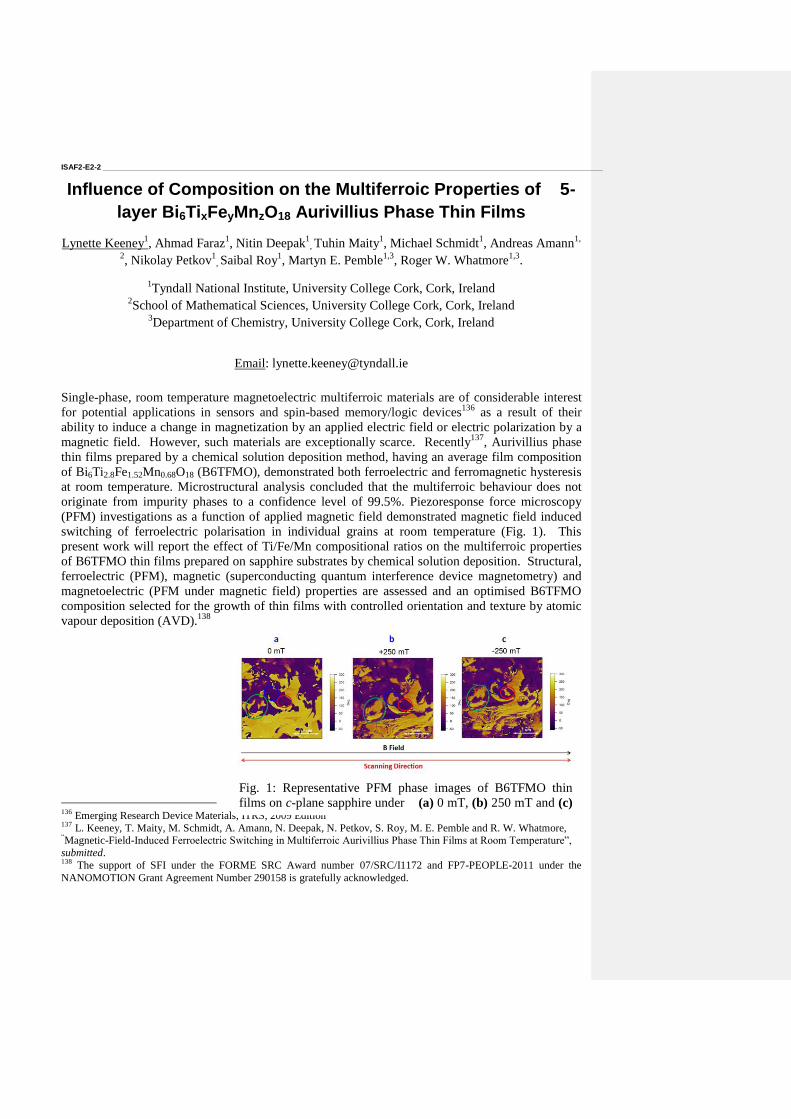
ISAF2-E2-2 _____________________________________________________________________________________________________________________
Influence of Composition on the Multiferroic Properties of 5-
layer Bi6TixFeyMnzO18 Aurivillius Phase Thin Films
Lynette Keeney1, Ahmad Faraz
1, Nitin Deepak
1, Tuhin Maity
1, Michael Schmidt
1, Andreas Amann
1,
2, Nikolay Petkov
1, Saibal Roy
1, Martyn E. Pemble
1,3, Roger W. Whatmore
1,3.
1Tyndall National Institute, University College Cork, Cork, Ireland
2School of Mathematical Sciences, University College Cork, Cork, Ireland
3Department of Chemistry, University College Cork, Cork, Ireland
Email: [email protected]
Single-phase, room temperature magnetoelectric multiferroic materials are of considerable interest
for potential applications in sensors and spin-based memory/logic devices136
as a result of their
ability to induce a change in magnetization by an applied electric field or electric polarization by a
magnetic field. However, such materials are exceptionally scarce. Recently137
, Aurivillius phase
thin films prepared by a chemical solution deposition method, having an average film composition
of Bi6Ti2.8Fe1.52Mn0.68O18 (B6TFMO), demonstrated both ferroelectric and ferromagnetic hysteresis
at room temperature. Microstructural analysis concluded that the multiferroic behaviour does not
originate from impurity phases to a confidence level of 99.5%. Piezoresponse force microscopy
(PFM) investigations as a function of applied magnetic field demonstrated magnetic field induced
switching of ferroelectric polarisation in individual grains at room temperature (Fig. 1). This
present work will report the effect of Ti/Fe/Mn compositional ratios on the multiferroic properties
of B6TFMO thin films prepared on sapphire substrates by chemical solution deposition. Structural,
ferroelectric (PFM), magnetic (superconducting quantum interference device magnetometry) and
magnetoelectric (PFM under magnetic field) properties are assessed and an optimised B6TFMO
composition selected for the growth of thin films with controlled orientation and texture by atomic
vapour deposition (AVD).138
136
Emerging Research Device Materials, ITRS, 2009 Edition 137
L. Keeney, T. Maity, M. Schmidt, A. Amann, N. Deepak, N. Petkov, S. Roy, M. E. Pemble and R. W. Whatmore,
“Magnetic-Field-Induced Ferroelectric Switching in Multiferroic Aurivillius Phase Thin Films at Room Temperature”,
submitted. 138
The support of SFI under the FORME SRC Award number 07/SRC/I1172 and FP7-PEOPLE-2011 under the
NANOMOTION Grant Agreement Number 290158 is gratefully acknowledged.
Fig. 1: Representative PFM phase images of B6TFMO thin
films on c-plane sapphire under (a) 0 mT, (b) 250 mT and (c)
-250 mT.
Fig. 1: Representative PFM phase images of B6TFMO thin
films on c-plane sapphire under (a) 0 mT, (b) 250 mT and (c)
-250 mT.

ISAF2-E2-3 _____________________________________________________________________________________________________________________
Application of PMN-PT ferroelectric relaxor for multiferroic
random access memory cell
Nicolas Tiercelin1, Yannick Dusch
1, Alexey Klimov
2, Stefano Giordano
1, Arnaud Stolz
1, Vladimir
Preobrazhensky3 and Philippe Pernod
1
International Associated Laboratory LICS/LEMAC : 1IEMN UMR CNRS 8520, PRES Lille Nord de France, ECLille, Villeneuve d'Ascq, France 2V. A. Kotel’nikov Institute of Radioengineering and Electronics, 125009 Moscow, Russia
3Wave Research Center, GPI RAS, Moscow, Russia
Email: [email protected] - [email protected]
The renaissance of multiferroics139
has triggered a quest for magnetoelectric memories, offering
non-volatility, endurance, high switching speeds and ultra-low power operation. In 2010, Tiercelin
et al.140
proposed a concept for magnetoelectric random access memory (MELRAM) based on
stress-mediated composite multiferroic. Theoretical studies of the expected performances have been
presented141
and a macroscopic proof of the concept was provided 142
. In this system electric field
allows switching between two orthogonal magnetic states ''0'' or ''1'' in plane of magnetostrictive
subsystem. In order to be successfully integrated in practical devices, one must find an efficient way
to generate inplane anisotropic stress in a simple planar structure with vertical dielectric
polarisation. We show here that the ferroelectric relaxors of the PMN-PT type, cut in the <011>
plane are suitable candidates for MELRAM cell
design. For demonstration we sputtered the
magnetostrictive nanostructure
10*[(TbCo2)5nm/(FeCo)5nm] on commercial <011>
PMN-PT single crystal substrate (fig.1). A
magnetic easy axis (EA) was induced in plane by
application of static magnetic field during
sputtering. External magnetic field HS
perpendicular to the EA created two energetically
equivalent magnetic states. Application of a
positive voltage pulse to the planar electrodes
induced orientation of magnetisation in the position
''1'', whereas a negative pulse switched
magnetisation to the position ''0''. The switching
process was detected by magneto-optic Kerr effect
(MOKE). The results of MOKE signal
measurements are shown on fig.1. The
139
N. Spaldin, and M. Fiebig, Science, 309 (5733), 391-392, 2005. 140
N. Tiercelin, Y. Dusch, V. Preobrazhensky, and P. Pernod, J. Appl. Phys. 109, 07D726, 2011. 141
S. Giordano, Y.Dusch, N. Tiercelin, P. Pernod and V. Preobrazhensky, Phys.Rev.B 85, 155321,2012. 142
N. Tiercelin, Y. Dusch, A. Klimov, S. Giordano, V. Preobrazhensky, P. Pernod, Appl.Phys.Lett. 99, 192507, 2011
Fig. 41: Prototype of MELRAM cell and
experimental evidence of by electric field
magnetisation switching in magnetostrictive
nanostructure deposited on single crystal PMN-PT
substrate.

characteristics of cell and prospective of MELRAM technology are discussed.
ISAF2-E2-4 _____________________________________________________________________________________________________________________
Spin dynamics controlled by strain in BiFeO3 films
Daniel Sando1, Arsène Agbelele
3, Dovran Rahmedov
4, Ingrid C. Infante
2, Alexander Pyatakov
6,
Laurent Bellaiche4, Stephane Fusil
1, Cecile Carretero
1, Eric Jacquet
1, Cyrile Deranlot
1, Sergey
Lisenkov7, Dawei Wang
8, Jean-Marie Le Breton
3, Maximilien Cazayous
5, Alain Sacuto
5, Jean
Juraszek3, Anatoly Zvezdin
6, Agnès Barthélémy
1, Brahim Dkhil
2, Manuel Bibes
1
1Unité Mixte de Physique CNRS/Thalès UMR137, Palaiseau, France 2Ecole Centrale Paris/CNRS UMR8580, Chatenay-Malabry, France
3Université de Rouen/CNRS UMR6634, Rouen, France
4Physics Department, University of Arkansas, Fayetteville, Arkansas, United States
5Université Paris 7/CNRS UMR7162, Paris, France
6Russian Academy of Sciences, Moscow, Russian Federation
7University of South Florida, Tampa, FL, United States
8Xi’an Jiaotong University, Xi’an,China
Email: [email protected]
Multiferroics are considered as ideal materials to combine magnetic control of polarization and
conversely, electric control of magnetization, as they show (within the same phase) ferroelectric and
magnetic orders. Among these materials, BiFeO3 has been by far the most investigated, mainly
because it is one of the few room temperature multiferroics. Bulk BiFeO3 is characterized by a large
ferroelectric polarization coexisting with a G-type antiferromagnetic order and a spin cycloid. When
grown in thin film form, the epitaxial strain has been shown to induce important distortions on unit
cell causing a drift of the ferroelectric transition143
and eventually the stabilization of new phases144
.
In the present work145
, we explore the less studied effects of epitaxial strain on spin dynamics of
BiFeO3 films. By combining Mössbauer and Raman spectroscopies with Landau-Ginzburg and
effective Hamiltonian calculations, we have evidenced that a spin cycloid modulation exists in
BiFeO3 thin films at small and moderate strains and disappears at high tensile and compressive
strains. We have also observed that the average spin orientation evolves from in-plane to out of
plane directions when the strain changes from compressive to tensile, which leads to a strong
modification of spin dynamics in these films. The interface effects and coupling to other
ferromagnetic layers through exchange bias effects will also be presented and discussed in the spirit
of proposing and proving direct applications in tuning the conduction in giant magnetoresistive spin
valves.
143
I. C. Infante et al. Phys. Rev. Lett. 105, 057601 (2010) 144
R. J. Zeches et al. Science 326, 977 (2009) ; B. Dupé et al., Phys. Rev. B 81, 144128 (2010) 145
D. Sando et al., Nature Materials, in press
ISAF2-E2-5 _____________________________________________________________________________________________________________________
On the chemical stability and charged point defects in BiFeO3-
materials
Tor Grande1
1Department of Materials Science and Engineering,
Norwegian University of Science and Technology, NO-7491 Trondheim, Norway
Email: [email protected]
The rhombohedral perovskite BiFeO3 has become the centre of research on multiferroics due to its
robust room-temperature multiferroism with a Néel temperature of 370 °C and a Curie temperature
of 820–830 °C.146
Beside the multferroic properties BiFeO3 is also interesting because of its high
intrinsic polarization of ~ 100 μC/cm2, which is along the pseudocubic (111) direction. A
tremendous amount of work has been reported on BiFeO3 thin films, single crystals and bulk
ceramics,1 but particularly the investigations on bulk BiFeO3 ceramics have been hampered by the
severe difficulties to prepare single phase materials and the problems with dielectric loss caused by
the high electronic conductivity of BiFeO3.
We will first focus on the thermodynamic stability of BiFeO3, particularly with respect to the
competing reaction to form the phases Bi25FeO39 and Bi2Fe4O9 on the expense of BiFeO3.147
The
thermodynamic stability of BiFeO3 and related Bi-based perovskites is discussed in relation to
Goldschmidt tolerance factor and the influence of pressure/strain and chemical substitution.
The thermodynamic stability and properties of BiFeO3 is also influenced by the volatility of Bi2O3
at elevated temperatures. The corresponding loss of PbO in PZT materials is known to have a
pronounced effect on the functional properties of traditional lead-based ferroelectric materials, and
here will discuss possible influence of charged point defects in the BiFeO3-materials due to loss of
Bi2O3. Volatilization of Bi2O3 will create charged point defects in the perovskite lattice, more
precisely Bi and O vacancies. These point defects may have detrimental effects on the properties of
bulk BiFeO3 ceramics mainly due to two different reasons.
First, the oxygen vacancies formed due to Bi2O3 loss may influence on the oxidations state Fe and
thereby on the electrical conductivity of BiFeO3. Iron is Fe3+
in stoichiometric BiFeO3, but may
oxidize to Fe4+
due to available oxygen vacancies leading to increasing p-type conductivity.148
We
will discuss the influence of the atmosphere during thermal annealing by examples from (1-x)
Bi0.5K0.5TiO3 – x BiFeO3 (BKT-BFO) solid solutions.149
Finally, point defects may also strongly influence on the domain wall mobility in BiFeO3, as
recently discussed by Rojac et al.150
Strategies to reduce the influence of point defects and thereby
146
G. Catalan, J.F. Scott “Physics and applications of bismuth ferrite”, Adv. Mater., vol. 21, p. 2463 -2485, 2009. 147
S.M. Selbach et al. “On the thermodynamic stability of BiFeO3”, Chem. Mater., vol. 21, p. 169-173, 2009. 148
S.M. Selbach, T. Tybell, M.-A. Einarsrud, T. Grande “Phase transitions, electrical conductivity and chemical
stability of BiFeO3 at high temperature”, J. Solid State Chem., vol. 183, p. 1205-1208, 2010. 149
M. I. Morozov, M.-A. Einarsrud, T. Grande., “Polarization and strain response in Bi0.5K0.5TiO3 – BiFeO3 ceramics”,
Appl. Phys. Lett., vol. 101, 252904, 2012. 150
T. Rojac, M. Kosec, B. Budic, N. Setter, D. Damjanovic “Strong ferroelectric domain-wall pinning in BiFeO3
ceramics”, J. Appl. Phys. vol. 108, 074107, 2010.

softening of BiFeO3 is discussed with particular emphasis on the atmosphere during annealing and
chemical substitution of Fe with Ti, which reduces the oxygen vacancy concentration.

PFM4
CLUB C
Tuesday, July 23 2013, 02:00 pm - 03:30 pm
Chair: To Be Aannounced
PFM-E3-1 ______________________________________________________________________________________________________________________
Polarization-Related Electronic Properties of Complex Oxides
Alexei Gruverman
Department of Physics and Astronomy, University of Nebraska, Lincoln, NE 68588, USA
Recently it was demonstrated that the conductivity of the LaAlO3/SrTiO3 (LAO-STO)
interface can be reversibly tuned through a switchable electromechanical response arising from the
LAO overlayer in the LAO-STO heterostructures. Bulk LaAlO3 (LAO) is a typical perovskite,
which shows paraelectric behavior at room temperature. In this study, we have investigated
switchable dielectric propeties of the LAO ultrathin (several unit cells) films grown on top of
lattice-matched conducting oxide Sr0.2Ca0.8RuO3 (SCRO) on the (001) (LaAlO3)0.3–(Sr2AlTaO3)0.7
(LSAT) substrate. Piezoresponse force microscopy (PFM) studies performed on the
LAO/SCRO/LSAT heterostructures show a genuine switchable hysteretic electromechanical
behavior resembling that one observed in ferroelectric films associated with induced polarization in
the LAO layer. An insight into the underlying mechanism of such behavior has been gained by
using temperature-dependent PFM spectroscopic, dielectric and structural measurements. The effect
of inhomogeneous strain gradient induced by the PFM probe on polarization in LAO has been also
studied. The proposed mechanism of switchable electromechanical response should be active in
many other oxide heterosystems, but its detailed manifestation likely depends on a number of
subtleties, such as oxygen octahedra rotations and distortions, strain, and lattice coupling at the
nanoscale. Control of this phenomenon will enable new structures and devices that exploit
nanoscale electromechanical coupling.

PFM-E3-2 ______________________________________________________________________________________________________________________
Minimum domain size and stability in carbon nanotube-
ferroelectric devices
Cédric Blaser and Patrycja Paruch
MaNEP-DPMC, University of Geneva, Switzerland
Email: [email protected]
When combining carbon nanotubes (CNTs) with ferroelectric materials, the small size and
exceptional electronic properties of the former makes them extremely interesting as local field
sources for nanoscale ferroelectric polarization switching. Meanwhile, the ferroelectric polarization
can be used to modulate the electronic behavior of an adjacent CNT, leading to potentially
multifunctional devices.
We deposited single-walled CNTs from aqueous suspension onto patterned epitaxial ferroelectric
Pb(Zr0.2Ti0.8)O3 (PZT) thin films. Using this device, PFM is used to probe domain switching in
three different electrode configurations, using an AFM tip, edges of macroscopic planar electrodes
and CNTs on the ferroelectric surface as electric field sources, allowing us to separately consider
the effects of the separation between two straight domain walls, and the radius of curvature on
domain stability151
.
Domain growth dynamics in the three configurations are discussed using finite element analysis of
the vertical electric field vs. distance dependence, and in comparison with previously reported
ferroelectric nanodomains and thermodynamic models of switching.
In 270 nm thick films, we demonstrate domain sizes down to 9 nm half-with using a CNT electrode
(see Fig. 1) and 14.5 nm radius with the AFM tip as electrode, two times smaller than the minimum
domain size predicted from thermodynamic models. The observed domains remained stable over 20
months. These results suggest that the internal defect structure plays a significant role in the
dynamic and stability of ferroelectric nanodomains.
Fig. 1: (a) PFM phase image
after a +10 V, 10 µs pulse,
with the switched domain
following the shape of the
electrically connected CNT.
Zoom on the thinnest
continuous domain in (b)
PFM phase and (c) PFM
amplitude. (d) PFM phase
and amplitude signals across
the outlined area in (b)/(c).
151
C. Blaser and P. Paruch, “Minimum domain size and stability in carbon nanotube -ferroelectric device”, Appl. Phys.
Lett., vol. 101, p. 142906, 2012.

PFM-E3-3 ______________________________________________________________________________________________________________________
Piezo and ferroelectric phases of glycine
Ensieh Hosseini1, Igor Bdikin
2, Budhendra Singh
2, Vladimir Bystrov
1, Andrei Kholkin
1
1 CICECO & Department of Materials and Ceramics Engineering, University of Aveiro, Aveiro,
Portugal 2 TEMA & Department of Mechanical Engineering, University of Aveiro, Aveiro, Portugal
Email: [email protected]
Creating artificial biomimetic materials with multiple functions similar to those of living bodies, is
an important frontier for advanced society in near future. Recently, electromechanical coupling in
many bio-organic materials has been revisited and several materials demonstrated properties similar
to their inorganic counterparts. Glycine (the simplest amino acid) is one of basic and important
elements in biology as it serves as building block for proteins. Several polymorphic forms with
completely different physical properties are possible in glycine. In this work, glycine microcrystals
were grown on a conductive substrate under different conditions. The influence of various
parameters (e.g. concentration of solution, solvent, volume of microdroplets, temperature, humidity,
and type of substrates) on the formation of polymorph phases was evaluated using powder X-ray
diffraction. The results indicated that the saturated solution and lower temperature lead to formation
of γ phase whereas the β phase can be grown from low concentrated solution.
The piezoelectric response and ferroelectric domains of the different polymorphic forms of glycine
crystals have been investigated locally by using Piezoresponse Force Microscopy (PFM). The
domain switching properties are studied for crystals by applying a dc voltage to a localized area.
The results showed that the switching domains growth in different shape depends on the
polarization direction of the sample.
In addition, a molecular dynamics simulation was used for modeling the crystal structure of glycine
and the spontaneous polarization was determined and compared with experimental results. Also, the
mechanisms of polarization switching on the nanoscale level were investigated via this model.
The major part of this work was supported by the Marie-Curie ITN project “Nanomotion”
PFM-E3-4 ______________________________________________________________________________________________________________________
Piezoelectricity in Biopolymers and
DNA Nucleobase Crystals
Brian J. Rodriguez1
1School of Physics, University College Dublin, Ireland
Email: [email protected]
Piezoelectricity is a property of many organic and biological materials, including collagen,
nucleobase crystals, and peptide nanostructures. Recent progress in understanding the origin and
role of piezoelectricity and possible ferroelectricity in these materials will be discussed.
Piezoelectric properties of collagen, etc. can be measured using piezoresponse force microscopy
(PFM), which is a voltage-modulated contact mode atomic force microscopy technique that allows
bias-induced surface deformations via the converse piezoelectric effect to be detected. Thus, PFM
makes it possible to investigate electromechanical coupling in biosystems and organic materials at
the nanoscale.
Recently, PFM was used to study polar ordering in tendon, eye tissues, and collagen
hydrogels.152,153
Collagen shear piezoelectricity is a functional property that may be associated with
bone remodeling, however, the biofunctional implications of piezoelectricity in collagen and other
biomaterials has yet to be clearly demonstrated. A preliminary step towards this goal is to determine
if collagen is piezoelectric in physiological conditions, which involves understanding the role of pH
and moisture content. Here, we investigate the structure and piezoelectric properties of aligned
collagen membranes before and after a neutralization process, which alters the pH from acidic to
neutral conditions. Electromechanical properties of the collagen membranes have been further
investigated under controlled humidity conditions to probe whether collagen is piezoelectric in
moisture rich environments. In addition, the orientation dependence of collagen fibril piezoresponse
is explored using cross sections of embedded tendons.
An early biopolymer identified as being piezoelectric was deoxyribonucleic acid (DNA).154
DNA
comprises the nucleobases adenine, cytosine, guanine, and thymine, which are held by backbones of
deoxyribose and phosphate. Thymine and other nucleobase crystals grown from solutions during
evaporation have been found to exhibit piezoelectricity, and in some cases contain domains which
can be switched via external field. The results are complemented using second harmonic generation
measurements.
The discovery of piezoelectricity in peptide nanotubes has helped to propel the field of PFM of
biomaterials. Peptides are short chains of amino acids and are the building blocks of all structural
tissues and are inherently “biocompatible.” Not only are peptide nanotubes piezoelectric but so are
dried peptide hydrogels. The differences in piezoresponse from the two materials will be analyzed.
152
D. Denning et al. “Visualizing Molecular Polar Order in Tissues via Electromechanical Coupling”, J. Struc t. Bio.,
vol. 180, p. 409–419, 2012. 153
D. Denning et al. “Electromechanical properties of dried tendon and iso-electrically focused collagen hydrogels”,
Acta Biomater., vol. 8, p. 3073–3079, 2012. 154
E. Fukada “History and recent progress in piezoelectric polymers”, IEEE Trans. Ultra. Ferro. Freq. Control, vol. 47,
1277-1290 2000.

Furthermore, the outlook for future measurements and applications of piezoelectric collagen,
nucleobase crystals, and peptide nanostructures will be discussed.

Lead-free ceramics: Spectroscopy
CLUB A
Tuesday, July 23 2013, 04:30 pm - 06:00 pm
Chair: Jirka Hlinka
Institute of Physics, Czech Academy of Sciences
ISAF3-F1-1 _____________________________________________________________________________________________________________________
Two excitations below phonon frequencies in broad-band
dielectric response of Ba(Zr,Ti)O3 ceramics
Dmitry Nuzhnyy1, Jan Petzelt
1, Maxim Savinov
1, Viktor Bovtun
1, Martin Kempa
1,
Giovanna Canu2, Maria Teresa Buscaglia
2, Vincenzo Buscaglia
2
1Department of Dielectrics, Institute of Physics, Academy of Sciences of the Czech Republic,
Prague, Czech Republic 2Electroceramic Department, Institute for Energetics and Interphases, National Research Council
Genoa, Italy
Email: [email protected]
Lead-free perovskite systems attract attention due to their potential use in a wide range of
applications (piezoelectric transducers, phase shifters, tunable filters etc.). They are considered as
good candidates for the replacement of lead-based materials. Dielectric properties of the
Ba(Zr,Ti)O3 solid solution are changing dramatically with the ratio of Zr/Ti-ions. This allows for
tuning the dielectric properties from slightly incipient ferroelectric behaviour (BaZrO3) through
relaxor to diffuse and normal ferroelectric behavior (BaTiO3).
We have already investigated a set of Ba(Zr,Ti)O3 ceramics155
and observed an excitation which
softened from THz either to GHz (BaZr0.2Ti0.8O3) or to MHz (BaZr0.4Ti0.6O3) range where it merged
into a constant-loss background. This feature in dielectric response we considered as one
overdamped excitation associated with local hopping of Ti-ions among their off-centered sites. To
prove this picture, we needed similar data for smaller Ti concentration, since the hopping dynamics
of Ti ions is not expected to be much dependent on the size of the Ti clusters. In order to obtain
these data we prepared another set of Ba(Zr,Ti)O3 ceramics with higher concentration of Zr (x=0.6,
0.7, 0.8) using solid-state reaction technique. These compounds were studied in 5 - 500 K
temperature range using Fourier-transform infrared reflectivity, time-domain THz transmission
spectroscopy, high-frequency - microwave coaxial technique, and standard low-frequency
capacitance spectroscopy. This enabled us to obtain the dielectric response in the whole range from
1Hz to 100 THz and fit it with phenomenological models.
Even though there is a gap in our experimental data (~109-10
11 Hz), careful fitting of the data at
various temperatures led us to the conclusion that two relaxations are needed to fit the dielectric
response in the whole frequency range. The high frequency relaxation (~1010
-1011
Hz) is almost
temperature independent for all investigated compounds, while another broad relaxation is
thermally activated, showing considerable softening on cooling from GHz range, similar for all
compositions in agreement with the Ti-hopping picture.
155
D. Nuzhnyy, J. Petzelt, M. Savinov, T. Ostapchuk, V. Bovtun, M. Kempa, J. Hlinka, V. Buscaglia, M. T. Buscaglia,
and P. Nanni, “Broadband dielectric response of Ba(Zr,Ti)O3 ceramics: From incipient via relaxor and diffuse up to
classical ferroelectric behavior”, Phys. Rev. B, vol. 86, p. 014106(1)- 014106(9), 2012.
ISAF3-F1-2 _____________________________________________________________________________________________________________________
Impedance spectroscopy studies on Mn doped K0.5Na0.5NbO3
lead-free ferroelectric ceramics
Paula Maria Vilarinho, Muhammad Asif Rafiq, Maria Elisabete Costa,
Department of Materials and Ceramics Engineering, Centre for Research in Ceramics and
Composite Materials, CICECO, University of Aveiro, 3810-193 Aveiro, Portugal
Email: [email protected]
This talk is about a systematic study carried out by impedance spectroscopy to identify defects and
describe their role in the conduction behaviour of undoped and Mn doped KNN ceramics. Oxygen
vacancies located at the grain boundaries were identified as responsible for the decrease of the
conductivity at room temperature and a less leaky behaviour of Mn doped KNN and also for the
conduction increase at elevated temperatures for these ceramics. The importance of this work
resides on the fact that K0.5Na0.5NbO3 (KNN) is one of the leading lead free piezoelectric materials
being considered as an alternative to Pb(Zrx,Ti1-x)O3 (PZT), which is currently the most widely used
material for electromechanical applications156
.
Smart materials like piezoelectrics and ferroelectrics are crucial in applications such as sensors and
actuators, radio-frequency switching, drug delivery, chemicals detection, and power generation and
storage. Although pure KNN has inferior electromechanical properties compared to PZT, efforts are
on going to tailor and improve its ferroelectric and piezoelectric coefficients by doping and
texturing1. Earlier reports have shown that the remnant polarization (Pr) values of KNN ceramics
may exceed the saturation polarization value157
, thus indicating the presence of leakage current and
space charge contributions either in undoped or doped KNN (doped with Li and Ta, Li and Sb)
ceramics. Mn dopant has been used to reduce the leakage current in KNN single crystals but its
effects on the electrical properties of KNN ceramics have not yet been properly addressed and thus
remain unclear.
In this work Impedance spectroscopy (IS) is used to get a deeper insight into the electrical
behaviour of undoped and Mn doped KNN ceramics by assessing and distinguishing contributions
to the ceramic impedance arising from different regions, bulk and grain-boundary. Ac conductivity
dependence on the temperature showed that resistivity of Mn doped ceramics increased at room
temperature while the reverse was observed for temperature higher than 200 °C. Activation energy
values showed that hopping mechanism at room temperature and mobile oxygen vacancies are the
main charge carrier at high temperature (T˃200 °C). Impedance spectroscopy revealed the main
location of the defects and the dependence of their contribution on the temperature. For low
temperatures, Mn decreases the conductivity of KNN and for high temperatures due to the increased
mobility of oxygen vacancies mainly located at the grain boundaries, the conductivity of Mn doped
KNN increases. This work is expected to contribute to the pool of knowledge on KNN materials
making them useable for industrial applications.
156
Y. Saito, H. Tani, et al., Lead-free piezoceramics. Nature, 432(7013), p. 84-87, 2004 157
H.E. Mgbemere, M. Hinterstein, et al., Structural phase transitions and electrical properties of (KxNa1-x)NbO3 based
ceramics modified with Mn. Journal of the European Ceramic Society, 32(16), p. 4341-4352, 2012

ISAF3-F1-3 _____________________________________________________________________________________________________________________
defect-structure – property relationships: fundamental
differences between Pb[Zr,Ti]O3 and ‘lead-free’ alternative
compounds
Rüdiger-A. Eichel
Forschungszentrum Jülich, Institut für Energie und Klimaforschung (IEK-9), Germany
Email: [email protected]
In order to meet the sometimes stringent requirements for specific piezoelectric applications, the
materials properties of ferroelectric oxides may be tailored by means of aliovalent doping with
transition-metal or rare-earth ions. The main effect of aliovalent doping is to control the defect
structure in terms of the generation or annihilation of lattice vacancies158
, which renders compounds
with so-termed 'hard' or 'soft' ferroelectric properties. With that respect, the hardening mechanism is
attributed to the formation of dipolar complexes between the acceptor ion and charge compensating
oxygen vacancies. As a result, the orientation of spontaneous polarization in the neighbouring unit
cells as well as the domain structure and domain-wall mobility are impacted.
By using multi-frequency electron paramagnetic resonance (EPR) spectroscopy159
, local
information at the (paramagnetic) dopant sites can be gathered, including information about the
dopant site with respect to domain walls or grain boundaries160
. Recent results allow to monitor the
formation of defect complexes between acceptor-type dopants and charge-compensating oxygen
vacancies. Furthermore, a complete defect chemical description upon aliovalent doping emerges
from the EPR results.
Most interestingly, the results obtained for the pseudo-binary solid-solution system
Pb[Zr1-xTix]O3 (PZT) cannot simply be transferred to ‘lead-free’ alternative compounds, such as
[Ka0.5Na0.5]NbO3 (KNN)161
or [Bi0.5Na0.5]TiO3 (BNT)162
for instance. Differences in defect
structure also impact the dynamic properties as function of switching upon external poling163
.
158
E. Erdem, P. Jakes, S.K.S. Parashar, K. Kiraz, M. Somer, A. Rüdiger, R.-A Eichel,
J. Phys.: Condens. Matter 22 (2010) 345901. 159
R.-A. Eichel, Phys. Chem. Chem. Phys., 13 (2011) 368–384. 160
P. Jakes, E. Erdem, R.-A. Eichel, L. Jin, D. Damjanovic, Appl. Phys. Lett. 98 (2011) 072907. 161
E. Erünal, P. Jakes, S. Körbel, J. Acker, H. Kungl, C. Elsässer, M.J. Hoffmann, R.-A. Eichel,
Phys. Rev. B 84 (2011) 184113. 162
E. Aksel, P. Jakes, E. Erdem, D.M. Smyth, A. Ozarowski, J. van Tol, J.L. Jones, R.-A. Eichel,
J. Am. Ceram. Soc., 94 (2011) 1363–1367. 163
L.X. Zhang, E. Erdem, X. Ren, R.-A. Eichel, Appl. Phys. Lett. 93 (2008) 202901
ISAF3-F1-4 _____________________________________________________________________________________________________________________
Ferroelectric Phase Transition in nanostructured BaTiO3 studied by
Raman scattering and second harmonic generation.
A. M. Pugachev1, V. I. Kovalevskii
1, V. K. Malinovsky
1, N. V. Surovtsev
1, Yu. M. Borzdov
2
1Institute of Automation and Electrometry, Russian Academy of Sciences, Novosibirsk, Russia
2 V. S. Sobolev Institute of Geology and Mineralogy, Russian Academy of Sciences, Novosibirsk,
Russia
E-mail [email protected]
It is widely known that the ferroelectric phase transition from tetragonal to cubic phase in
BaTiO3 ceramics and powders is strongly suppressed compared with the crystals. In our study the
features of this transition were investigated by low - frequency Raman scattering and second
harmonic generation (SHG) techniques. The samples were prepared from the BaTiO3 powder
pressed by using a uniaxial pressure of 600 MPa, 3*103 MPa and 4*10
3 MPa. Raman scattering
spectra were measured in a spectral range 1.5 – 650 cm-1
by a triple-grating spectrometer
TRIVISTA 777 for temperature range from 300 K to 800 K, covering both ferroelectric and
paraelectric phases. Over the entire temperature range a well pronounced central peak (CP) was
detected. It was previously shown1,2
that in BaTiO3 crystals the central peak in a spectral density
presentation 1 )(nT,IT,In (here n() is the Bose factor) is well fitted by Lorentz
contour (single relaxation time approximation) and its width demonstrated a critical slowing down
in the vicinity of the Curie temperature. In the case of single relaxation time the low frequency part
of CP in a susceptibility presentation is described by power law: T,IT,I nr where
and = 1. In contrast to crystals the CP in a spectral density presentation in a pressed powder can
not be fitted by Lorentz function and T,Ir where 0.07 in ferroelectric phase and
increased up to 0.8 with increasing the temperature up to 800 K in paraelectric phase. Such behavior
of the parameter indicates that the relaxation process in the pressed powder can not be described
by a single relaxation time. The temperature dependence of is typical for ferroelectrics with a
diffuse phase transition (relaxors) as shown by the example of crystals SBN 613 and PMN
4.
A study of second harmonic generation (SHG) in BaTiO3 pressed powder has been carried out by
the procedure described in5. It was found that the broadening of the phase transition is significantly
increased with the application of mechanical stress and increases monotonically with increasing
stress up to Burns temperature (~ 600 K). The experimental data confirm that BaTiO3 ceramics and
powders in paraelectric phase exhibit much greater SHG intensity than in the crystals because of the
existence of the polar nanoregions in the paraelectric phase.
The obtained results of Raman and SHG experiments are interpreted as a relaxor - like behavior of
BaTiO3 pressed powder.
1. J.H. Ko, T. H.Kim, K. Roleder, D. Rytz, S. Kojima, “Precursor dynamics in the ferroelectric phase transition of
barium titanate single crystals studied by Brillouin light scattering” Phys. Rev. B 84, 094123, 2011 2. V. K. Malinovsky, A. M. Pugachev, V.A. Popova, N. V. Surovtsev, S. Kojima “Low frequency Raman scattering
in BaTiO3 crystal”, Feroelectrics, in press 3. Koreeda, H. Taniguchi, S. Saikan, and M. Itoh “Fractal Dynamics in a Single Crystal of a Relaxor Ferroelectric”,
PRL, 109, 197601, 2012 4. V. K. Malinovsky, A. M. Pugachev, N. V. Surovtsev “Study of the Central Peak in Raman Spectra of SBN
Crystals” Bulletin of the Russian Academy of Sciences: Physics, 74, No. 9, pp. 1231–1234, 2010.

5. Pugachev A.M., Kovalevskii V.I., Surovtsev N.V., Kojima S., Prosandeev S.A., Raevski I.P., Raevskaya S.I.
“Broken local symmetry in paraelectric BaTiO3 proved by second harmonic generation”, P.R.L., v.108., 247601,
2012 .
ISAF3-F1-5 _____________________________________________________________________________________________________________________
Non-linear Coupling between the Primary and Secondary Order
Parameters of Strontium Titanate Ceramics
Ali Al-Zein1, Bernard Hehlen
2, Christine Bogicevic
3, Pascale Gemeiner
3, Jean-Michel Kiat
3,4
1European Synchrotron Radiation Facility, 6 Rue Jules Horowitz, Grenoble, France
2Laboratoire Charles Coulomb (LCC), CNRS-UMR 5221, Université Montpellier II, France
3Laboratoire Structures, Propriétés et Modélisation des Solides, Ecole Centrale Paris, CNRS-
UMR8580, Châtenay Malabry, France 4Laboratoire Léon Brillouin, CE Saclay CNRS-UMR12, Gif-Sur-Yvette, France
Email: [email protected]
SrTiO3 (STO) is a textbook example of quantum paraelectric materials with very high value of the
dielectric constant at low temperature. It exhibits an anti-ferrodistortive cubic (Pm-3m) to tetragonal
(I4mcm) phase transition at Ta = 105 K [1]. In bulk material, its primary (rotation angle of the
TiO6 octahedra) and secondary (spontaneous strain c/a-1) order parameters are linearly coupled
with 2 c/a-1. In STO ceramics, a core-shell structure was assumed to interpret the behavior of
the low-temperature permittivity, with probably a static polarization in the shell and large stress
fields affecting the core grain [2].
Neutron diffraction, Raman and hyper-Raman (HRS) scattering have been used to study the
structural and vibrational properties of micrograin and nanograin STO ceramics. HRS spectroscopy
of micrograin STO ceramics revealed a splitting of the soft F1u mode into a A2u and Eu vibrations
[3]. This was not observed by previous Raman scattering or infrared absorption studies.
Interestingly, this splitting occurs at about
90 K that is, at a much lower temperature
than 160 K [4] at which the tilting of the
TiO6 octahedra starts growing. This
observation suggests a nonlinear coupling
between the two order parameters (Figure)
[3]. Such behavior possibly arises from the
strain field the shell imposes on the core
grain and one therefore expects that it is
strongly dependent on the synthesis route
and grain size.
[1] K.A. Muller, W. Berlinger, and F. Waldner, Phys. Rev. Lett. 21, 814 (1968).
[2] J. Petzelt, T. Ostapchuk, I. Gregora, P. Kuzel, J. Liu, and Z. Shen, J. Phys.: Condens. Matter. 19, 196222 (2007).
[3] B. Hehlen, A. Al-Zein, C. Bogicevic, P. Geimener, and J-M. Kiat, Phys. Rev. B 87, 014303 (2013).

[4] J. M. Kiat, C. Bogicevic, P. Geimener, A. Al-Zein, F. Karolak, N. Guiblin, F. Porcher, B. Hehlen, Ll. Yedra, S.
Estradé, F. Peiro and R. Haumont, Phys. Rev. B. 87, 024106 (2013).

Multiferroics
CLUB B
Tuesday, July 23 2013, 04:30 pm - 06:00 pm
Chair: Tor Grande
Norwegian University of Science and Technology
ISAF3-F2-1 _____________________________________________________________________________________________________________________
Raman spectroscopy for characterization of crystalline phases
and phase transformations in BiVO4 and BiFeO3 films
D. A. Tenne1, A. K. Farrar
1, J. B. Romero
1, D. A. Hillsberry
1, S. Stoughton,
2 M. Showak,
2 , C.
Heikes2, J. H. Lee
2, A. Melville
2, C. Adamo
2, Q. Mao,
3 L. F. Kourkoutis,
3 D. A. Muller,
3 C.
Beekman4, W. Siemons,
4 T.Z. Ward
4, M. Chi,
4 J. Howe,
4 M.D. Biegalski
5, N. Balke
5, P.
Maksymovych5, H. M. Christen
4, and D. G. Schlom
2
1Department of Physics, Boise State University, Boise, ID 83725, USA
2 Department of Materials Science and Engineering, Cornell University, Ithaca, NY 14853, USA
3 School of Applied and Engineering Physics, Cornell University, Ithaca, NY 14853, USA
4Materials Science and Technology Division, Oak Ridge National Laboratory, Oak Ridge, TN,
37831, USA 5Center for Nanophase Materials Sciences, Oak Ridge National Laboratory, Oak Ridge, TN, 37831,
USA
Email: [email protected]
Raman spectroscopy is a technique capable of distinguishing crystalline polymorphs and detecting
phase transitions between different crystal structures in bulk and thin film solids. In this work it was
applied to study strained thin films of photocatalytic BiVO4 and multiferroic BiFeO3. Bulk BiVO4
is known to exist in several crystalline forms (polymorphs), and the monoclinic polymorph of
BiVO4 is believed to have the best photocatalytic properties for water splitting using solar energy.
The BiV04 films studied were grown by molecular beam epitaxy on yittria-stabilized cubic zirconia
substrate. Raman spectra were measured at 10 and 300 K with several excitation laser lines in the
range from 325 to 514.5 nm, and 441.6 nm line was found to produce the strongest Raman signal
from BiVO4, because of its proximity to the resonance with the bandgap of BiVO4. The analysis of
the Raman spectra indicated that the film was of monoclinic structure, as expected for the growth
conditions used and consistent with x-ray diffraction and scanning transmission electron
microscopy data.
Coherently strained BiFeO3 films were grown by molecular beam epitaxy and pulsed laser
deposition on various substrates including YAIO3, LaAIO3, NdGaO3, SrTiO3, and ReScO3 (Re = Pr,
Sm, Gd, Tb, Dy). These substrates induce lattice-mismatch biaxial strain in BiFeO3 films spanning
a range from –6.7% to +1.4%. The films have been studied by variable-temperature Raman
spectroscopy with ultraviolet excitation (325 nm) in order to reduce the substrate contribution to
spectra. At low temperatures, a large number of BiFeO3 phonon peaks observed in spectra indicates
the structure to be monoclinically distorted (Cc). Temperature evolution of Raman spectra from
BiFeO3 films under large compressive strain (above 4%) indicates the phase transitions to another
monoclinic phase, then to tetragonal phase (at ~ 730 K for the films on LaAlO3). Raman spectra
(measured up to 950 K), demonstrate that the high temperature phases are still polar; a linear
extrapolation of Raman intensities yields an estimated Curie temperature at 867 100 C for
BiFeO3 under 4.4% compressive strain. Tensile-strained films (on PrScO3 substrates, strain +1.4%)
undergo a transition from monoclinic rhombohedral-like to orthorhombic-like phase at about 550–
600 K. The temperature dependence of Raman intensities of certain characteristic peaks indicates
the possibility of coexisting phases in the temperature range 400–550 K.

Supported in part by the National Science Foundation through the Grant DMR-1006136.
ISAF3-F2-2 _____________________________________________________________________________________________________________________
Electromagnons and sequence of structural and magnetic phase
transitions in multiferroic CaMn7O12 S. Kamba
1, V. Goian
1, F. Kadlec
1, J. Hejtmánek
1, M. Savinov
1, P. Vaněk
1, and M. Orlita
2
1Institute of Physics, Academy of Sciences of the Czech Republic, Prague, Czech Republic
2Grenoble High Magnetic Field Lab, Grenoble, France
Email: [email protected]
CaMn7O12 is an unusual material which exhibits a rich sequence of structural, ferroelectric and
magnetic phase transitions. At high temperatures, (CaMn3)Mn4O12 crystallizes in the cubic
perovskite structure (space group Im3 ) and upon cooling below Tc1 ~ 450 K charge ordering occurs
which induces a structural transition to a trigonal phase with the space group 3R (Z=3). Below Tc2
=250 K, orbital ordering occurs and the trigonal structure becomes incommensurately modulated
with a propagation vector qc=(0,0,2.077).164
Upon further cooling below TN1=90 K, an
incommensurately modulated magnetic structure emerges with a magnetic modulation vector qm =
½qc.164 Very recently, it was reported165
that the magnetic structure is also ferroelectric with a
spontaneous polarization attaining up to Ps=2870 Cm-2
oriented parallel to the c axis. This is the
highest spin-induced polarization among all multiferroics. At TN2=50 K, another magnetic transition
occurs, giving rise to a second propagation vector along the c axis. Both propagation vectors qm1
and qm2 change with temperature, but their average value corresponds exactly to ½qc.
We have investigated far-IR reflectivity and time-domain THz transmission spectra of CaMn7O12
between 10 and 550 K and found significant changes in the spectra at structural and magnetic phase
transitions. The IR reflectivity changes abruptly at Tc1 = 450 K, giving evidence of the first-order
character of the phase transition. Moreover, the conductivity seen in the high-temperature IR
spectra disappears below Tc1, proving the metal-insulator character of this phase transition due to
charge ordering. New polar phonons appear in the spectra in the incommensurate phase below 250
K due to a change of IR selection rules. Close to TN1, a new mode develops near 50 cm-1
; another
one near 30 cm-1
appears below TN2. Since the modes appear near the magnetic phase transitions,
they can be spin waves (magnons). Nevertheless, IR reflectivity spectra reveal a transfer of the
oscillator strengths from the phonons to the excitations seen below 50 cm-1
. Thus, the modes at 30
and 50 cm-1
contribute to the dielectric permittivity and not to the magnetic susceptibility. This is a
typical signature of electromagnons, i.e. electric active magnons, which are activated in THz
dielectric spectra due to dynamical magnetoelectric coupling. The origin of magnetoelectric
coupling in CaMn7O12 will be analyzed and discussed.
Low-temperature far-IR transmission spectra measured under magnetic field up to 12 T revealed
significant shifts of electromagnon frequencies with magnetic field. These shifts are responsible for
a large dependence of low-frequency dielectric permittivity on applied static magnetic field
(magneto-dielectric effect), which we as well investigated.
164
N.J. Perks, R.D. Johnson, C. Martin, L.C. Chapon, and P.G. Radaeli, “Magneto-orbital helices as a route to coupling
magnetism and ferroelectricity in multiferroic CaMn7O12 ”, Nature Commun.vol. 3, p. 1277, 2012. 165
R.D. Johnson, L.C. Chapon, D.D. Khalyavin, P. Manuel, P.G. Radaeli, and C. Martin, “Giant improper
ferroelectricity in the ferroaxial magnetic CaMn7O12”, Phys. Rev. Lett. vol. 108, p. 067201 (2012).
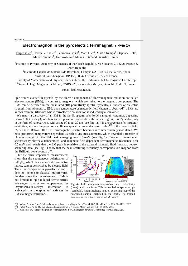
ISAF3-F2-3 _____________________________________________________________________________________________________________________
Electromagnon in the pyroelectric ferrimagnet ε-Fe2O3
Filip Kadlec1, Christelle Kadlec
1 , Veronica Goian
1, Martí Gich
2, Martin Kempa
1, Stéphane Rols
3,
Maxim Savinov1, Jan Prokleška
4, Milan Orlita
5 and Stanislav Kamba
1
1Institute of Physics, Academy of Sciences of the Czech Republic, Na Slovance 2, 182 21 Prague 8,
Czech Republic
2Institut de Ciència de Materials de Barcelona, Campus UAB, 08193, Bellaterra, Spain
3Institut Laue-Langevin, BP 156, 38042 Grenoble Cedex 9, France
4Faculty of Mathematics and Physics, Charles Univ., Ke Karlovu 5, 121 16 Prague 2, Czech Rep.
5Grenoble High Magnetic Field Lab, CNRS - 25, avenue des Martyrs, Grenoble Cedex 9, France
Email: [email protected]
Spin waves excited in crystals by the electric component of electromagnetic radiation are called
electromagnons (EMs), in contrast to magnons, which are linked to the magnetic component. The
EMs can be detected in the far-infared (IR) permittivity spectra; typically, a transfer of dielectric
strength from phonons to EMs upon temperature or magnetic field change is observed166
. EMs are
known from multiferroics whose ferroelectric polarization is induced by a spin order.
We report a discovery of an EM in the far-IR spectra of ε-Fe2O3 nanograin ceramics, appearing
below 100 K. ε-Fe2O3 is a less known phase of iron oxide with the space group Pna21, stable only
in the form of nanoparticles with a size of about 30 nm (see Fig. 1). It is a charge transfer insulator,
exhibiting, at room temperature, a collinear spin structure and a record value167
of the coercive field,
Hc ≃20 kOe. Below 110 K, its ferrimagnetic structure becomes incommensurately modulated. We
have performed temperature-dependent IR reflectivity measurements, which revealed a transfer of
phonon strength to the EM peak emerging near 10 meV (see Fig. 1). Terahertz time-domain
spectroscopy shows a temperature- and magnetic-field-dependent ferromagnetic resonance near
0.5 meV and reveals that the EM peak is sensitive to the external magnetic field. Inelastic neutron
scattering data (see Fig. 1) show that the peak scattering frequency corresponds to a magnon from
the Brillouin zone boundary168
.
Our dielectric impedance measurements
show that the spontaneous polarization of
ε-Fe2O3, which has a non-centrosymmetric
lattice, cannot be switched by electric field.
Thus, the compound is pyroelectric and it
does not belong to classical multiferroics;
the data show that the existence of EMs is
not limited to spin-induced ferroelectrics.
We suggest that at low temperatures, the
Dzyaloshinskii-Moriya interaction is
activated, tilts the spins and activates the
EM via magnetostriction.
166
R. Valdés Aguilar & al.,“Colossal magnon-phonon coupling in Eu0.75Y0.25MnO3”, Phys.Rev.B, vol.76, 60404(R), 2007 167
J. Tuček & al., “ε-Fe2O3: An advanced nanomaterial ...”, Chem. Mater. vol. 22, p. 6483-6505, 2010 168
C. Kadlec & al., “Electromagnon in ferrimagnetic ε-Fe2O3 nanograin ceramics”, submitted to Phys. Rev. Lett.
Fig. 42: Left: temperature-dependent far-IR reflectivity
(lines) and data from THz transmission spectroscopy
(symbols). Right: Inelastic neutron scattering map of the
powdered sample (pictured in the inset). The framed
area marks the mixed magnon-EM branch.

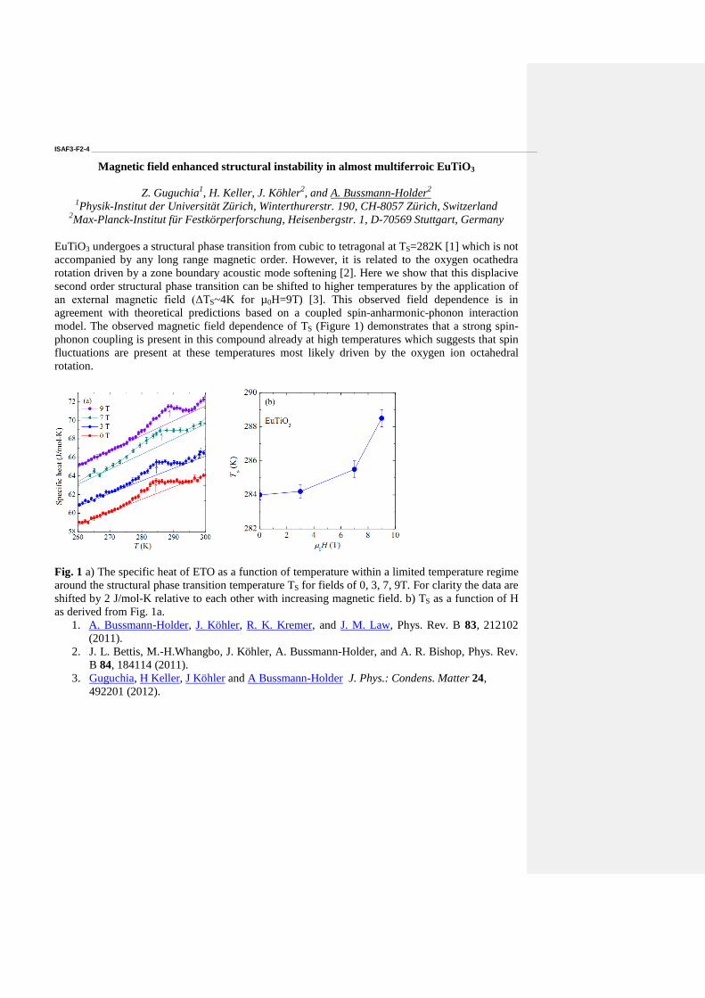
ISAF3-F2-4 _____________________________________________________________________________________________________________________
Magnetic field enhanced structural instability in almost multiferroic EuTiO3
Z. Guguchia1, H. Keller, J. Köhler
2, and A. Bussmann-Holder
2
1Physik-Institut der Universität Zürich, Winterthurerstr. 190, CH-8057 Zürich, Switzerland
2Max-Planck-Institut für Festkörperforschung, Heisenbergstr. 1, D-70569 Stuttgart, Germany
EuTiO3 undergoes a structural phase transition from cubic to tetragonal at TS=282K [1] which is not
accompanied by any long range magnetic order. However, it is related to the oxygen ocathedra
rotation driven by a zone boundary acoustic mode softening [2]. Here we show that this displacive
second order structural phase transition can be shifted to higher temperatures by the application of
an external magnetic field (ΔTS~4K for µ0H=9T) [3]. This observed field dependence is in
agreement with theoretical predictions based on a coupled spin-anharmonic-phonon interaction
model. The observed magnetic field dependence of TS (Figure 1) demonstrates that a strong spin-
phonon coupling is present in this compound already at high temperatures which suggests that spin
fluctuations are present at these temperatures most likely driven by the oxygen ion octahedral
rotation.
Fig. 1 a) The specific heat of ETO as a function of temperature within a limited temperature regime
around the structural phase transition temperature TS for fields of 0, 3, 7, 9T. For clarity the data are
shifted by 2 J/mol-K relative to each other with increasing magnetic field. b) TS as a function of H
as derived from Fig. 1a.
1. A. Bussmann-Holder, J. Köhler, R. K. Kremer, and J. M. Law, Phys. Rev. B 83, 212102
(2011).
2. J. L. Bettis, M.-H.Whangbo, J. Köhler, A. Bussmann-Holder, and A. R. Bishop, Phys. Rev.
B 84, 184114 (2011).
3. Guguchia, H Keller, J Köhler and A Bussmann-Holder J. Phys.: Condens. Matter 24,
492201 (2012).
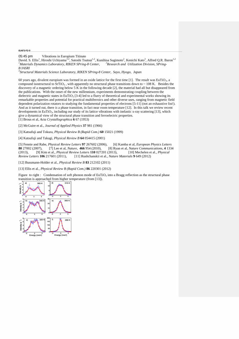
ISAF3-F2-5 _____________________________________________________________________________________________________________________
05:45 pm Vibrations in Europium Titinate
David. S. Ellis1, Hiroshi Uchiyama
1,2, Satoshi Tsutsui
1,2, Kunihisa Sugimoto
2, Kenichi Kato
3, Alfred Q.R. Baron
1,2
1Materials Dynamics Laboratory, RIKEN SPring-8 Center,
2Research and Utilization Division, SPring-
8/JASRI 3Structural Materials Science Laboratory, RIKEN SPring-8 Center, Sayo, Hyogo, Japan
60 years ago, divalent europium was formed in an oxide lattice for the first time [1]. The result was EuTiO3, a
compound isostructural to SrTiO3 , with apparently no structural phase transitions down to ~ 108 K. Besides the
discovery of a magnetic ordering below 5 K in the following decade [2], the material had all but disappeared from
the publications. With the onset of the new millennium, experiments demonstrating coupling between the
dielectric and magnetic states in EuTiO3 [3-4] led to a flurry of theoretical and experimental works showing its
remarkable properties and potential for practical multiferroics and other diverse uses, ranging from magnetic field
dependent polarization rotators to studying the fundamental properties of electrons [5-11] (not an exhaustive list!).
And as it turned out, there is a phase transition, in fact near room temperature [12]. In this talk we review recent
developments in EuTiO3, including our study of its lattice vibrations with inelastic x-ray scattering [13], which
give a dynamical view of the structural phase transition and ferroelectric properties.
[1] Brous et al, Acta Crystallographica 6 67 (1953)
[2] McGuire et al., Journal of Applied Physics 37 981 (1966)
[3] Katsufuji and Tokura, Physical Review B (Rapid Com.) 60 15021 (1999)
[4] Katsufuji and Takagi, Physical Review B 64 054415 (2001)
[5] Fennie and Rabe, Physical Review Letters 97 267602 (2006), [6] Kamba et al, European Physics Letters
80 27002 (2007), [7] Lee et al, Nature, 466 954 (2010), [8] Ryan et al, Nature Communications, 4 1334
(2013), [9] Kim et al., Physical Review Letters 110 027201 (2013), [10] Mechelen et al., Physical
Review Letters 106 217601 (2011), [11] Rushchanskii et al., Nature Materials 9 649 (2012)
[12] Bussmann-Holder et al., Physical Review B 83 212102 (2011)
[13] Ellis et al., Physical Review B (Rapid Com.) 86 220301 (2012)
Figure to right : Condensation of soft phonon mode of EuTiO3 into a Bragg reflection as the structural phase
transition is approached from higher temperature (from [13]).

PZT film processing
CLUB C
Tuesday, July 23 2013, 04:30 pm - 06:00 pm
Chair: Nazanin Bassiri-Gharb
Georgia Institute of Technology
ISAF2-F3-1 _____________________________________________________________________________________________________________________
Solution Chemistry, Substrate, and Processing Effects on
Chemical Homogeneity of PZT Thin Films
Jon F. Ihlefeld,1 Paul G. Kotula,
1 Geoff L. Brennecka,
1 Christopher T. Shelton,
1 Bonnie B.
McKenzie,1 Bryan Gauntt,
1 Dara V. Gough,
1 Ping Lu,
1 and Erik D. Spoerke
1
1Sandia National Laboratories, Albuquerque, New Mexico/USA
Email: [email protected]
In this presentation we explore the contributing factors toward preparing high-quality chemically-
homogeneous lead zirconate titanate (PZT) thin films via chemical solution routes. Principle to this
study is the selection of an adhesion layer that forms a low energy interface with platinum on
SiO2/Si substrates, resulting in improved dielectric and ferroelectric responses of PbZr0.52Ti0.48O3.
PZT films deposited on substrates with ZnO adhesion layers have 35% and 21% percent
enhancements over traditional titanium adhesion layers in remanent polarization and permittivity,
respectively, with values of 32 µC/cm and 1950 measured. Enhanced responses have been ascribed
to films deposited on ZnO-buffered substrates possessing no composition gradients as determined
from chemical mapping utilizing quantitative Energy Dispersive Spectroscopy within in a Scanning
Transmission Electron Microscope. Films prepared on traditional substrates possess significant
gradients in the Ti/Zr concentrations. To understand this observation we have explored the effects
of solution chemistry (traditional sol-gel versus chelate), pyrolysis temperature, substrate adhesion
layer, and crystallization anneal heating rate on chemical gradient formation and subsequent
properties in PZT films. In the course of this study, we have found that films prepared on
Pt/ZnO/SiO2/Si substrates possess homogeneous distributions of zirconium and titanium through
the film thickness regardless of solution chemistry and pyrolysis condition. PZT films prepared on
conventional Pt/Ti/SiO2/Si substrates possess enriched concentrations of titanium near the PZT/Pt
interface in all cases. We will show that this chemical gradient is driven by diffusion of titanium
from the adhesion layer through the platinum bottom electrode. Finally, we will show our most
recent studies investigating the effect of crystallization heating rate within a rapid thermal annealer
on the gradient formation for films prepared on Pt/ZnO/SiO2/Si substrates. Sandia National
Laboratories is a multi-program laboratory managed and operated by Sandia Corporation, a wholly
owned subsidiary of Lockheed Martin Corporation, for the U.S. Department of Energy's National
Nuclear Security Administration under contract DE-AC04-94AL85000.
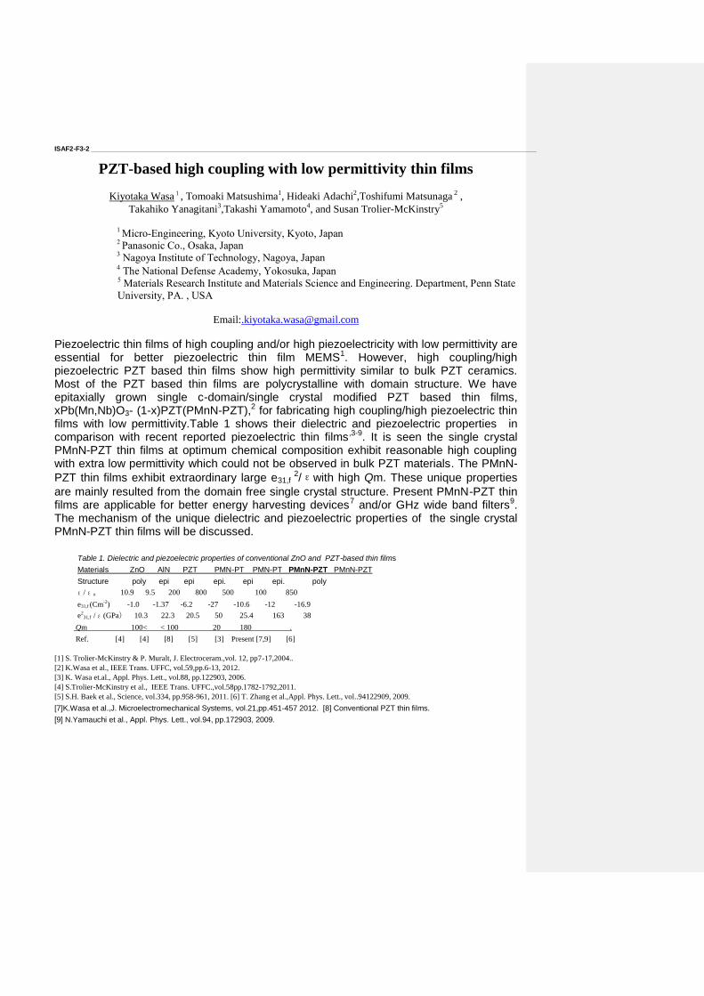
ISAF2-F3-2 _____________________________________________________________________________________________________________________
PZT-based high coupling with low permittivity thin films
Kiyotaka Wasa1, Tomoaki Matsushima1, Hideaki Adachi
2,Toshifumi Matsunaga
2 ,
Takahiko Yanagitani3,Takashi Yamamoto
4, and Susan Trolier-McKinstry
5
1 Micro-Engineering, Kyoto University, Kyoto, Japan
2 Panasonic Co., Osaka, Japan
3 Nagoya Institute of Technology, Nagoya, Japan 4 The National Defense Academy, Yokosuka, Japan 5 Materials Research Institute and Materials Science and Engineering. Department, Penn State
University, PA. , USA
Email:[email protected]
Piezoelectric thin films of high coupling and/or high piezoelectricity with low permittivity are essential for better piezoelectric thin film MEMS1. However, high coupling/high piezoelectric PZT based thin films show high permittivity similar to bulk PZT ceramics. Most of the PZT based thin films are polycrystalline with domain structure. We have epitaxially grown single c-domain/single crystal modified PZT based thin films, xPb(Mn,Nb)O3- (1-x)PZT(PMnN-PZT),2 for fabricating high coupling/high piezoelectric thin films with low permittivity.Table 1 shows their dielectric and piezoelectric properties in comparison with recent reported piezoelectric thin films,3-9. It is seen the single crystal PMnN-PZT thin films at optimum chemical composition exhibit reasonable high coupling with extra low permittivity which could not be observed in bulk PZT materials. The PMnN-
PZT thin films exhibit extraordinary large e31,f 2/εwith high Qm. These unique properties
are mainly resulted from the domain free single crystal structure. Present PMnN-PZT thin films are applicable for better energy harvesting devices7 and/or GHz wide band filters9. The mechanism of the unique dielectric and piezoelectric properties of the single crystal PMnN-PZT thin films will be discussed.
Table 1. Dielectric and piezoelectric properties of conventional ZnO and PZT-based thin films
Materials ZnO AlN PZT PMN-PT PMN-PT PMnN-PZT PMnN-PZT
Structure poly epi epi epi. epi epi. poly
ε/εo 10.9 9.5 200 800 500 100 850
e31,f (Cm-2) -1.0 -1.37 -6.2 -27 -10.6 -12 -16.9
e231,f /ε(GPa) 10.3 22.3 20.5 50 25.4 163 38
Qm 100< < 100 20 180 .
Ref. [4] [4] [8] [5] [3] Present [7,9] [6]
[1] S. Trolier-McKinstry & P. Muralt, J. Electroceram.,vol. 12, pp7-17,2004..
[2] K.Wasa et al., IEEE Trans. UFFC, vol.59,pp.6-13, 2012.
[3] K. Wasa et.al., Appl. Phys. Lett., vol.88, pp.122903, 2006.
[4] S.Trolier-McKinstry et al., IEEE Trans. UFFC.,vol.58pp.1782-1792,2011.
[5] S.H. Baek et al., Science, vol.334, pp.958-961, 2011. [6] T. Zhang et al.,Appl. Phys. Lett., vol..94122909, 2009.
[7]K.Wasa et al.,J. Microelectromechanical Systems, vol.21,pp.451-457 2012. [8] Conventional PZT thin films.
[9] N.Yamauchi et al., Appl. Phys. Lett., vol.94, pp.172903, 2009.
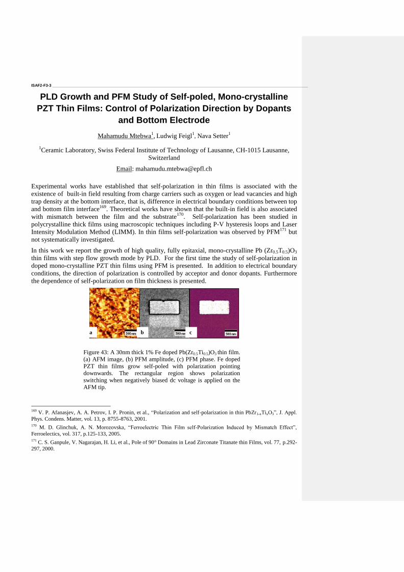
ISAF2-F3-3 _____________________________________________________________________________________________________________________
PLD Growth and PFM Study of Self-poled, Mono-crystalline
PZT Thin Films: Control of Polarization Direction by Dopants
and Bottom Electrode
Mahamudu Mtebwa1, Ludwig Feigl
1, Nava Setter
1
1Ceramic Laboratory, Swiss Federal Institute of Technology of Lausanne, CH-1015 Lausanne,
Switzerland
Email: [email protected]
Experimental works have established that self-polarization in thin films is associated with the
existence of built-in field resulting from charge carriers such as oxygen or lead vacancies and high
trap density at the bottom interface, that is, difference in electrical boundary conditions between top
and bottom film interface169
. Theoretical works have shown that the built-in field is also associated
with mismatch between the film and the substrate170
. Self-polarization has been studied in
polycrystalline thick films using macroscopic techniques including P-V hysteresis loops and Laser
Intensity Modulation Method (LIMM). In thin films self-polarization was observed by PFM171
but
not systematically investigated.
In this work we report the growth of high quality, fully epitaxial, mono-crystalline Pb (Zr0.5T0.5)O3
thin films with step flow growth mode by PLD. For the first time the study of self-polarization in
doped mono-crystalline PZT thin films using PFM is presented. In addition to electrical boundary
conditions, the direction of polarization is controlled by acceptor and donor dopants. Furthermore
the dependence of self-polarization on film thickness is presented.
169
V. P. Afanasjev, A. A. Petrov, I. P. Pronin, et al., “Polarization and self-polarization in thin PbZr1-xTixO3”, J. Appl.
Phys. Condens. Matter, vol. 13, p. 8755-8763, 2001. 170
M. D. Glinchuk, A. N. Morozovska, “Ferroelectric Thin Film self-Polarization Induced by Mismatch Effect”,
Ferroelectics, vol. 317, p.125-133, 2005. 171
C. S. Ganpule, V. Nagarajan, H. Li, et al., Pole of 90° Domains in Lead Zirconate Titanate thin Films, vol. 77, p.292-
297, 2000.
Figure 43: A 30nm thick 1% Fe doped Pb(Zr0.5Ti0.5)O3 thin film.
(a) AFM image, (b) PFM amplitude, (c) PFM phase. Fe doped
PZT thin films grow self-poled with polarization pointing
downwards. The rectangular region shows polarization
switching when negatively biased dc voltage is applied on the
AFM tip.
a c b
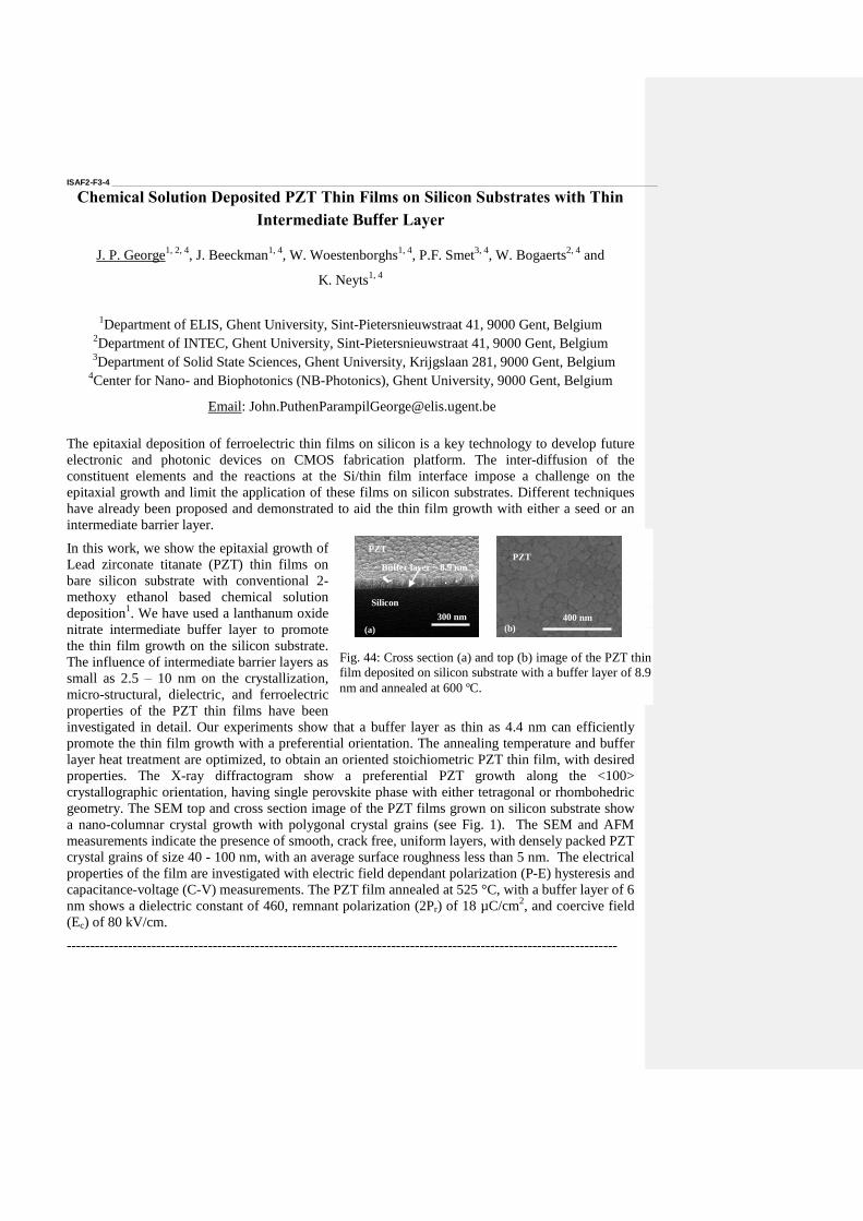
ISAF2-F3-4 _____________________________________________________________________________________________________________________
Chemical Solution Deposited PZT Thin Films on Silicon Substrates with Thin
Intermediate Buffer Layer
J. P. George1, 2, 4
, J. Beeckman1, 4
, W. Woestenborghs1, 4
, P.F. Smet3, 4
, W. Bogaerts2, 4
and
K. Neyts1, 4
1Department of ELIS, Ghent University, Sint-Pietersnieuwstraat 41, 9000 Gent, Belgium
2Department of INTEC, Ghent University, Sint-Pietersnieuwstraat 41, 9000 Gent, Belgium
3Department of Solid State Sciences, Ghent University, Krijgslaan 281, 9000 Gent, Belgium
4Center for Nano- and Biophotonics (NB-Photonics), Ghent University, 9000 Gent, Belgium
Email: [email protected]
The epitaxial deposition of ferroelectric thin films on silicon is a key technology to develop future
electronic and photonic devices on CMOS fabrication platform. The inter-diffusion of the
constituent elements and the reactions at the Si/thin film interface impose a challenge on the
epitaxial growth and limit the application of these films on silicon substrates. Different techniques
have already been proposed and demonstrated to aid the thin film growth with either a seed or an
intermediate barrier layer.
In this work, we show the epitaxial growth of
Lead zirconate titanate (PZT) thin films on
bare silicon substrate with conventional 2-
methoxy ethanol based chemical solution
deposition1. We have used a lanthanum oxide
nitrate intermediate buffer layer to promote
the thin film growth on the silicon substrate.
The influence of intermediate barrier layers as
small as 2.5 – 10 nm on the crystallization,
micro-structural, dielectric, and ferroelectric
properties of the PZT thin films have been
investigated in detail. Our experiments show that a buffer layer as thin as 4.4 nm can efficiently
promote the thin film growth with a preferential orientation. The annealing temperature and buffer
layer heat treatment are optimized, to obtain an oriented stoichiometric PZT thin film, with desired
properties. The X-ray diffractogram show a preferential PZT growth along the <100>
crystallographic orientation, having single perovskite phase with either tetragonal or rhombohedric
geometry. The SEM top and cross section image of the PZT films grown on silicon substrate show
a nano-columnar crystal growth with polygonal crystal grains (see Fig. 1). The SEM and AFM
measurements indicate the presence of smooth, crack free, uniform layers, with densely packed PZT
crystal grains of size 40 - 100 nm, with an average surface roughness less than 5 nm. The electrical
properties of the film are investigated with electric field dependant polarization (P-E) hysteresis and
capacitance-voltage (C-V) measurements. The PZT film annealed at 525 °C, with a buffer layer of 6
nm shows a dielectric constant of 460, remnant polarization (2Pr) of 18 µC/cm2, and coercive field
(Ec) of 80 kV/cm.
---------------------------------------------------------------------------------------------------------------------
Fig. 44: Cross section (a) and top (b) image of the PZT thin
film deposited on silicon substrate with a buffer layer of 8.9
nm and annealed at 600 ºC.
300 nm
Silicon
PZT
Buffer layer ~ 8.9 nm
(a) (b)
400 nm
PZT

1 Chen YN, Wang ZJ “Rapid Microwave Annealing of Amorphous Lead Zirconate Titanate Thin Films Deposited by Sol-Gel Method on
LaNiO3/SiO2/Si Substrates”. J. Am. Ceram. Soc. 96:90-5, 2013.
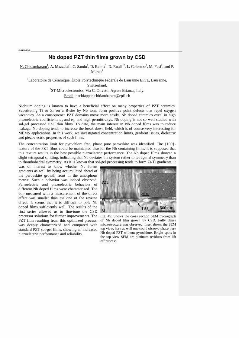
ISAF2-F3-5 _____________________________________________________________________________________________________________________
Nb doped PZT thin films grown by CSD
N. Chidambaram1, A. Mazzalai
1, C. Sandu
1, D. Balma
1, D. Faralli
2, L. Colombo
2, M. Fusi
2, and P.
Muralt1
1Laboratoire de Céramique, École Polytechnique Fédérale de Lausanne EPFL, Lausanne,
Switzerland. 2ST-Microelectronics, Via C. Olivetti, Agrate Brianza, Italy.
Email: [email protected]
Niobium doping is known to have a beneficial effect on many properties of PZT ceramics.
Substituting Ti or Zr on a B-site by Nb ions, form positive point defects that repel oxygen
vacancies. As a consequence PZT domains move more easily. Nb doped ceramics excel in high
piezoelectric coefficients dij and eij, and high permittivitys. Nb doping is not so well studied with
sol-gel processed PZT thin films. To date, the main interest in Nb doped films was to reduce
leakage. Nb doping tends to increase the break-down field, which is of course very interesting for
MEMS applications. In this work, we investigated concentration limits, gradient issues, dielectric
and piezoelectric properties of such films.
The concentration limit for pyrochlore free, phase pure perovskite was identified. The {100}-
texture of the PZT films could be maintained also for the Nb containing films. It is supposed that
this texture results in the best possible piezoelectric performance. The Nb doped films showed a
slight tetragonal splitting, indicating that Nb deviates the system rather to tetragonal symmetry than
to rhombohedral symmetry. As it is known that sol-gel processing tends to form Zr/Ti gradients, it
was of interest to know whether Nb forms
gradients as well by being accumulated ahead of
the perovskite growth front in the amorphous
matrix. Such a behavior was indeed observed.
Ferroelectric and piezoelectric behaviors of
different Nb doped films were characterized. The
e31,f measured with a measurement of the direct
effect was smaller than the one of the reverse
effect. It seems that it is difficult to pole Nb
doped films sufficiently well. The results of the
first series allowed us to fine-tune the CSD
precursor solutions for further improvements. The
PZT film resulting from this optimized process,
was deeply characterized and compared with
standard PZT sol-gel films, showing an increased
piezoelectric performance and reliability.
Fig. 45: Shows the cross section SEM micrograph
of Nb doped film grown by CSD. Fully dense
microstructure was observed. Inset shows the SEM
top view, here as well one could observe phase pure
Nb doped PZT without pyrochlore. Bright spots in
the top view SEM are platinum residues from lift
off process.

ISAF Group 2 Posters
Forum Hall
Tuesday, July 23 2013, 01:00 pm - 04:30 pm

ISAF-P2B-1 _____________________________________________________________________________________________________________________
Two-Stage Sintering of Multiferroic PZT-Based Ceramics
Supon Ananta1, Orawan Khamman
1, Penphitcha Amonpattaratkit
1
1Department of Physics and Materials Science, Faculty of Science, Chiang Mai University, Chiang
Mai, Thailand
Email: [email protected]
Highly dense and pure phase of nanograin ceramics are of current scientific and technological
interest, especially for utilization in electromagnetic components in which miniaturization and
integration are essential. In this respect, the processing challenge is to produce dense and pure phase
ceramics at low temperature, preferably without any additives and pressure, and with the least
amount of coarsening of the initial microstructure. Recently, the potential of a two-stage sintering
technique for the production of dense and pure phase ceramics with fine grain size has been
demonstrated by our group, especially in the area of electroceramics such as BaTiO3172
, PbTiO3,
Pb(Fe1/2Nb1/2)O3, Pb(Mg1/3Nb2/3)O3173
and Zn3Nb2O8174
ceramics. In this work, a two-stage
sintering, which exploits the difference in the kinetics between grain boundary diffusion and grain
boundary migration, was further employed to produce pure phase of perovskite multiferroic PZT-
based ceramics to high density with fine grain size, by suppressing grain growth in the final stage of
densification. It was found that this technique also offers an additional advantage as it requires a
substantially lower sintering temperature than conventional sintering.
172
W. Chaisan et al., “Two-stage sintering of barium titanate and resulting characteristics”,
Ferroelectrics., vol. 346, pp. 84-92, 2007. 173
R. Wongmaneerung et al., “Effect of two-stage sintering on phase formation, microstructure and
dielectric properties of perovskite PMN ceramics derived from a corundum Mg4Nb2O9 precursor”,
Mater. Chem. Phys., vol. 114, pp. 569-575, 2009. 174
P. Amonpattaratkit et al., “Microstructure and dielectric properties of Zn3Nb2O8 ceramics
prepared by a two-stage sintering method”, Ceram. Inter., 2013, in press.
ISAF-P2B-2 _____________________________________________________________________________________________________________________
Synthesis, Formation and Characterization of Perovskite Ferroelectric PZT-PZN Powders Derived from a Novel
Zn2Nb34O87 Precursor
Penphitcha Amonpattaratkit, Supon Ananta
Department of Physics and Materials Science, Faculty of Science,
Chiang Mai University, Chiang Mai 50200 Thailand
Email: [email protected]
Recently, there have been a great deal of interest in complex perovskite lead zirconate titanate-lead zinc niobate or PZT-
PZN systems because of their high dielectric, piezoelectric and ferroelectric properties suitable for applications in multilayer
capacitors, sensors and energy harvesting devices.1,2 Moreover, it is well documented that the inhomogeneous
mixing in the conventional solid state reaction process and firing temperature leads to formation of secondary phase (i.e. pyrochlore)
and subsequent deterioration of electrical properties in PZT-PZN ceramics.2,3 In this study, a combination of piezoelectric PZT perovskite phase stabilizers and novel Zn2Nb34O87 B-site precursor is employed for the fabrication of Pb(Zr0.44Ti0.56)O3-
Pb(Zn0.33Nb0.67)O3 powders. Effects of calcination temperature on phase formation, crystal structure,
morphology and microchemical composition of calcined PZT-PZN powders synthesized by a solid-
state reaction were carefully examined via a combination of X-ray diffraction (XRD), scanning
electron microscopy (SEM), transmission electron microscopy (TEM), particle size analyzer and
energy-dispersive X-ray (EDX) techniques. This study has demonstrated a successful fabrication of
pure-perovskite phase PZT-PZN powders via a combination of piezoelectric PZT perovskite phase
stabilizers and novel Zn2Nb34O87 B-site precursor. Moreover, with increasing calcination temperature, the
perovskite phase content, cell parameters, degree of tetragonality, particle size and degree of
agglomeration tend to increase.
________________________________________________
1 E. Fernandez, W.D. Mechtaly, M.Q. Lopez, B. Gnade, E.L. Salguero, P. Shah and H.N. Alshareel, “Synthesis and
Characterization of Pb(Zr0.53,Ti0.47)O3-Pb(Nb1/3,Zn2/3)O3 Thin Film Cantilevers for Energy Harvesting Applications”,
Smart. Mater. Res., vol. 2012 (doi:10.1155/2012/872439).
2 A. Ngamjarurojana, O. Khamman, S. Ananta and R. Yimnirun, “Synthesis, Formation and Characterization of Lead
Zinc Niobate-Lead Zirconate Titanate Powders Via a Rapid Vibro-Milling Method”, J. Electroceram., vol. 21 p. 786-
790, 2008.
3 N. Vittayakorn, G. Rujijanagul, X. Tan, H. He, M.A. Marquardt and D.P. Cann, “Dielectric Properties and
Morphotropic Phase Boundaries in the xPb(Nb1/3,Zn2/3)O3-(1-x)Pb(Zr0.5,Ti0.5)O3 Pseudo-Binary System”, J.
Electroceram., vol. 16 p. 141-149, 2006.
ISAF-P2B-3 _____________________________________________________________________________________________________________________
Influences of PZT Addition on the Phase Formation and Multiferroic Properties of PFN-Based Ceramics
Penphitcha Amonpattaratkit, Supon Ananta
Department of Physics and Materials Science, Faculty of Science,
Chiang Mai University, Chiang Mai 50200 Thailand
Email: [email protected]
Recently, many electromagnetic ceramics which are promising multiferroic candidate for
various electronic applications including transducers, capacitors and magnetoresistive random
access memory have been developed from binary systems containing a combination of relaxor and
normal ferroelectric materials.1 In connection with this, Pb(Fe0.5Nb0.5)O3 or PFN ceramics and their solid solu-
tions are one of the most promising multiferroic materials with a perovskite structure.2 However, the formation of unwanted phases
especially the pyrochlores are one of the major problems in the preparation of these PFN-based compounds.3 To solve this matter, in
this study, a combination of perovskite stabilizer Pb(Zr0.44Ti0.56)O3 or PZT and a wolframite-type FeNbO4 B-site
precursor was employed for the fabrication of PFN-PZT ceramics. The phase formation, microstructure and
multiferroic properties of ceramics in the (1-x)PFN-xPZT (x = 0.1-0.5) system were investigated by
using a combination of X-ray diffraction (XRD), scanning electron microscopy (SEM), energy-
dispersive X-ray (EDX) analyzer and the multiferroic measurement techniques. Phase-pure
perovskite of the PFN-PZT ceramics was obtained. These ceramics exhibit first-order ferroelectric
phase transition of typical normal ferroelectrics, where the dielectric response peaks are narrow,
sharp and without frequency dispersion, and the dielectric constant above Curie temperature (TC)
can be fitted well by Curie law. With the increase of PZT content, tetragonality value of the PFN-
PZT ceramics was found to increase slightly accompanied by the variation of cell volume, whilst
the P-E ferroelectric hysteresis loops become narrower accompanied by the decrease of remanent
polarization (Pr) and coercive field (EC).
________________________________________________
1 R. Wongmaneerung, P. Jantaratana, R. Yimnirun, S. Ananta, “Phase Formation and Magnetic Properties of Bismuth
Ferrite–Lead Titanate Multiferroic Composites”, J. Supercond. Nov. Magn., 2013 in press.
2 B. Fang, Y. Shan, K. Tezuka, H. Imoto, “High Curie Temperature Pb(Fe1/2Nb1/2)O3-Based Ferroelectrics:
0.40Pb(Fe1/2Nb1/2)O3–0.34PbZrO3–0.26PbTiO3”, Phys. Stat. Sol., vol. 202 p. 481-489 , 2005.
3 A. Prasatkhetragarn, “Synthesis and Dielectric Properties of 0.9Pb(Zr1/2Ti1/2)O3-0.1Pb(Fe1/3Nb2/3)O3 Ceramics”,
Ferroelectrics., vol. 416 p. 35-39, 2011.
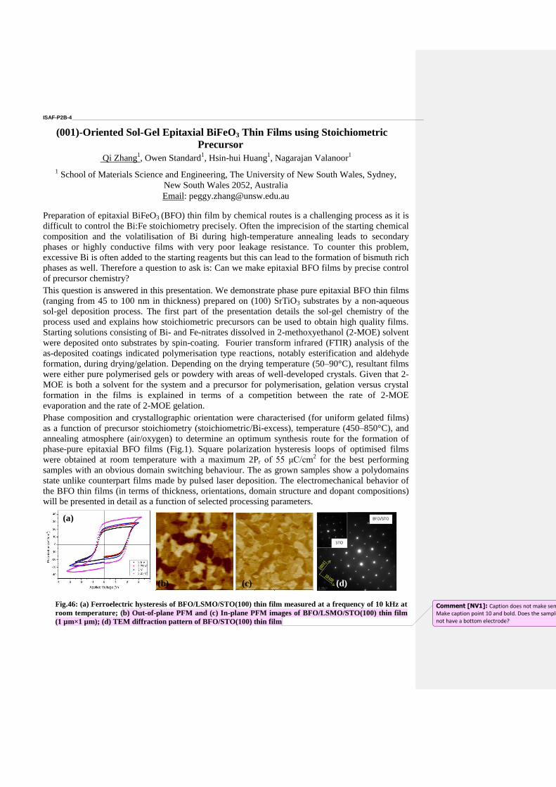
ISAF-P2B-4 _____________________________________________________________________________________________________________________
(001)-Oriented Sol-Gel Epitaxial BiFeO3 Thin Films using Stoichiometric
Precursor
Qi Zhang1, Owen Standard
1, Hsin-hui Huang
1, Nagarajan Valanoor
1
1 School of Materials Science and Engineering, The University of New South Wales, Sydney,
New South Wales 2052, Australia
Email: [email protected]
Preparation of epitaxial BiFeO3 (BFO) thin film by chemical routes is a challenging process as it is
difficult to control the Bi:Fe stoichiometry precisely. Often the imprecision of the starting chemical
composition and the volatilisation of Bi during high-temperature annealing leads to secondary
phases or highly conductive films with very poor leakage resistance. To counter this problem,
excessive Bi is often added to the starting reagents but this can lead to the formation of bismuth rich
phases as well. Therefore a question to ask is: Can we make epitaxial BFO films by precise control
of precursor chemistry?
This question is answered in this presentation. We demonstrate phase pure epitaxial BFO thin films
(ranging from 45 to 100 nm in thickness) prepared on (100) SrTiO3 substrates by a non-aqueous
sol-gel deposition process. The first part of the presentation details the sol-gel chemistry of the
process used and explains how stoichiometric precursors can be used to obtain high quality films.
Starting solutions consisting of Bi- and Fe-nitrates dissolved in 2-methoxyethanol (2-MOE) solvent
were deposited onto substrates by spin-coating. Fourier transform infrared (FTIR) analysis of the
as-deposited coatings indicated polymerisation type reactions, notably esterification and aldehyde
formation, during drying/gelation. Depending on the drying temperature (50–90°C), resultant films
were either pure polymerised gels or powdery with areas of well-developed crystals. Given that 2-
MOE is both a solvent for the system and a precursor for polymerisation, gelation versus crystal
formation in the films is explained in terms of a competition between the rate of 2-MOE
evaporation and the rate of 2-MOE gelation.
Phase composition and crystallographic orientation were characterised (for uniform gelated films)
as a function of precursor stoichiometry (stoichiometric/Bi-excess), temperature (450–850°C), and
annealing atmosphere (air/oxygen) to determine an optimum synthesis route for the formation of
phase-pure epitaxial BFO films (Fig.1). Square polarization hysteresis loops of optimised films
were obtained at room temperature with a maximum 2Pr of 55 μC/cm2 for the best performing
samples with an obvious domain switching behaviour. The as grown samples show a polydomains
state unlike counterpart films made by pulsed laser deposition. The electromechanical behavior of
the BFO thin films (in terms of thickness, orientations, domain structure and dopant compositions)
will be presented in detail as a function of selected processing parameters.
Fig.46: (a) Ferroelectric hysteresis of BFO/LSMO/STO(100) thin film measured at a frequency of 10 kHz at
room temperature; (b) Out-of-plane PFM and (c) In-plane PFM images of BFO/LSMO/STO(100) thin film
(1 µm×1 µm); (d) TEM diffraction pattern of BFO/STO(100) thin film
(b)
(a)
(c) (d)
Comment [NV1]: Caption does not make sense. Make caption point 10 and bold. Does the sample not have a bottom electrode?
ISAF-P2B-5 _____________________________________________________________________________________________________________________
Production and characterization of organic polar nanofibers
produced by electrospinning
Ricardo Lima, Tiago Monteiro, Pedro Sá, Etelvina de Matos Gomes, Bernardo Almeida and Dmitry
Isakov.
University of Minho, Center of Physics, Campus de Gualtar, 4710-059 Braga, Portugal
Email: [email protected]
Electrospinning is a versatile cost-effective bottom-up nanomanufacturing process, allowing for the
fabrication of continuous nanofibers with diameters ranging from a few nanometers up to
micrometers. In the last decade the interest in the electrospinning process and in the application of
electrospun nanofibers is exponentially growing, due to their potential applicability as active
material in electronic and sensor devices. The unique characteristics of electrospun nanofibers are
their high surface-to-volume ratio, intrinsic 3D topography, biochemical flexibility and the
possibility of obtaining extremely long fibers—all features which are strategically important for a
remarkable variety of technological applications. Additionally, functional embedded dopants
(included inorganic nanoparticles, carbon nanotubes, light-emitting molecules, cell-directing
proteins, conjugated polymers etc.) may greatly expand the use of electrospun nanofibers. The
recent success in the electrospinning of peptides and polymer-free materials is very encouraging for
the consideration of electrospinning as a bottom-up process for fabrication of various 1D organic
stand-alone nanofibers with strong π―π or h-bonding interactions served as molecular
entanglements for the stabilization of the continuous fiber-like structure.
Among the polar materials acting as functional elements in nanoelectronic devices, organic polar
materials are of special interest due to their attractive multifunctional capacity, making them very
attractive for a broad spectrum of potential applications in various fields such as thermoelectricity,
electromechanics, electro-optics etc. The attractiveness of nanosized polar materials results also
from the strong influence of the dimensionality on device performance and from the possibility of
tuning their polar properties by changing the molecular structure.
Here, we present an extended number of polar organic materials that can be successfully
electrospun. The materials under investigation include potassium sodium tartrate, triglycine
sulphate, glycine, DL-alanine, urea, L-cistine and sucrose. All materials are embedded into
electrospun nanofibers (with diameters in range of 200-600 nm) and possess strong dipolar
orientation along the fiber direction which were confirmed by X-ray diffraction measurements.
Aligned arrays of such obtained nanofibers present a mesocrystalline structure with highly
anisotropic responses. The study of polar properties such as ferroelectricity, pyroelectricity,
piezoelectricity and optical second harmonic generation are presented and discussed. All nanofibers
reveal an enhancement of polar responses as compared with their bulk counterparts. We propose
that the intrinsic orientation of polar molecules along electrospun nanofibers enhance the observed
cooperative phenomena.
ISAF-P2B-6 _____________________________________________________________________________________________________________________
Dielectric Properties of Ba1-xLaxTiO3 Ceramics Prepared by
Two-Step Sintering Method
Ferroelectric perovskite (ABO3) materials play an important role in modern electronics and
electronic engineering (capacitors, microwave technologies, etc.). Barium titanate (A = Ba, B = Ti)
has a special place in this group of compounds since solid solutions with high electrophysical and
ferroelectric properties based on it are obtained. Therefore, along with the constant improvement in
the technology of ceramic materials, an important area of modification of electrophysical
characteristics of the considered systems is doping by different iso-and heterovalent additives in A-
and B-sites, both separately and together. Rare earth elements are found to be more efficient in
comparison with other dopant additives. It was determined that the introduction of heterovalent
cations into the BaTiO3 lattice in A- and B- sites causes a significant change in its electrophysical
characteristics. The purpose of this work was to investigate the structure and ddielectric properties
of Ba1-xLaxTiO3 ceramics prepared by two-step sintering method.
By means of two-step sintering method Ba1-xLaxTiO3 (х = 0–0.05) ceramics with sub-micron
grain size was obtained. The grain size was 200–400 nm at x = 0.025 and 300–700 nm at x = 0.05.
Phase transition temperature was lowered with the growth of lanthanum concentration at the rate of
~25°С/mol%. Despite the small grain size the value of dielectric permittivity of the prepared
samples were increased (εmax ≈ (1.7–2.4)×104 for х = 0.025 and ≈ (3.3–4.7)×10
4 for х = 0.05) as
compared with large grain materials sintered by standard technique (with grain size > 1 µm).
Dielectric losses were at an acceptable level (tanδ ~ 0.05–0.15).
ISAF-P2B-7 _____________________________________________________________________________________________________________________
Effect of Oxygen Addition in the sputtering Gas on the
Structures and Dielectric Properties of Bi2Zn2/3Nb4/3O7 Thin
Films
M. Saeed Khan1,2
, Wei Ren1,2
, Peng Shi1,2
and Xiaoqing Wu1,2
1Electronic Materials Research Laboratory, Xi’an Jiaotong University, Xi’an, Shaanxi, China
2 International Center for Dielectric Research, Xi’an Jiaotong University, Xi’an, Shaanxi, China
Email: [email protected], [email protected]
Bi2Zn2/3Nb4/3O7 (BZN) thin films were deposited by RF magnetron sputtering technique onto
Pt/TiO2/SiO2/Si substrates at room temperature, without any intentional heating of substrate, as a
function of Ar/O2 atmosphere. As-deposited thin films were post- annealed at a temperature ≤ 200 oC, which is compatible with the printed circuit board (PCB) substrates. The effect of Ar/O2 gas
ratio on structures, surface morphologies, dielectric and electrical properties of thin films were
studied to produce dielectric thin films with suitable characteristics for application as an embedded
capacitor. Surface roughness increased with increasing the concentration of oxygen in Ar/O2 gas
ratio but the deposition rate reduced. Moderate oxygen enrichment is helpful for the stoichiometry
in the BZN films, which reduced the leakage current losses and the concentration of charge carriers
produced from oxygen vacancies. The dielectric properties were improved with varying the Ar/O2
gas ratio from 100/0 to 85/15 but no further significant improvement occurred with further variation
of the Ar/O2 gas ratio. The dielectric constant increased with increasing annealing temperature up to
150 oC due to the much stronger establishment of bismuth oxide into the thin film and then
decreases with further increase of temperature due to the Bi migration at high temperature. 200 nm-
thick BZN thin film deposited under Ar/O2 gas ratio of 85/15 and later post annealed at 150 oC had
a dielectric constant of 60.1 with a very low loss of 0.006, measured at 10 kHz. The leakage current
density was 6.7×10⁻⁷
A/cm2 at an applied bias field 400 kV/cm.
ISAF-P2B-8 _____________________________________________________________________________________________________________________
Electrical Activity of Ferroelectric Biomaterials
Přemysl Vaněk1, Zdeňka Kolská
2, Jan Petzelt
1
1Institute of Physics ASCR, Prague, Czech Republic
2J.E. Purkyně University, Ústí nad Labem, Czech Republic
Email: [email protected]
It is well known that bone is electrically active under mechanical loading, due to the piezoelectricity
of collagen and the movement of ionic fluids within the bone structure. Electrical potentials in
mechanically loaded bone have been linked to the mechanical adaptation of bone in response to
loading, leading to the suggestion that the addition of an electrically active component to an implant
material may improve healing and adaptation of the surrounding tissue. Recently, interest has
grown in exploiting this phenomenon to develop electrically active ceramics for implantation in
hard tissue, which may induce improved biological responses.
Ferroelectric (i.e. also piezoelectric) ceramics, which produce electrical potentials under stress, have
been among others studied in order to determine the possible benefits of using electrically active
bioceramics as implant materials. Most of the piezoelectric ceramics proposed for implant use
contain barium titanate (BaTiO3). In vivo and in vitro investigations have indicated that ceramics of
this kind are biocompatible and induce improved bone formation around implants. Nevertheless, the
results are somewhat ambiguous. In majority of them, a negative charge on the surface is preferred
for cell growth but in some cases a positive charge is preferred.
However, previous studies have not taken into account the fact that the charge at the surface of
ferroelectrics is always quickly compensated (screened) by the opposite charge from the
surroundings. Kalinin1 showed that the charge at the surface of polarized BaTiO3 (or the
ferroelectric domain) is fully screened by adsorbed charges at room temperature in air, so that the
charge on the surface is opposite to that of the polarization. If a ferroelectric is immersed in a liquid
(e.g. tissue fluid) it is obvious that an electric double layer and a diffusion layer are formed at its
surface. The charge distribution in these layers can be characterized in a simplified way by zeta
potential (potential at the „slipping“ plane). The zeta potential and its dependence on pH were
frequently measured on colloidal ferroelectric BaTiO3 particles because the zeta potential is crucial
for the stability of colloidal suspensions. However, the dependence of zeta potential on the polarity
of the surface of poled ferroelectrics has not been measured until now. Therefore it is not clear if the
spontaneous polarization in ferroelectrics can really have any influence on their bioactive behavior.
We shall measure the zeta potential in dependence of the surface polarity and pH on poled single
crystalline plates of ferroelectric LiNbO3 and BaTiO3. LiNbO3 will be used because of its good
stability of polarization, BaTiO3 because of its known biocompatibility. The zeta potential will be
determined by measurement of streaming potential with an electrolyte flowing in the gap between
two parallel ferroelectric plates.
______________________ 1S.V. Kalinin and D.A. Bonnell, “Local potential and polarization screening on ferroelectric surfaces”, Phys. Rev. B,
vol. 63, p. 125411-1-13, 2001.

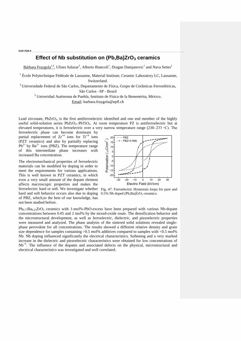
ISAF-P2B-9 _____________________________________________________________________________________________________________________
Effect of Nb substitution on (Pb,Ba)ZrO3 ceramics
Bárbara Fraygola1,2
, Ulises Salazar3, Alberto Biancoli
1, Dragan Damjanovic
1 and Nava Setter
1
1 École Polytechnique Fédérale de Lausanne, Material Institute, Ceramic Laboratory LC, Lausanne,
Switzerland. 2 Universidade Federal de São Carlos, Departamento de Física, Grupo de Cerâmicas Ferroelétricas,
São Carlos –SP - Brazil 3 Univeridad Autónoma de Puebla, Instituto de Física de la Benemérita, México.
Email: [email protected]
Lead zirconate, PbZrO3, is the first antiferroelectric identified and one end member of the highly
useful solid-solution series PbZrO3–PbTiO3. At room temperature PZ is antiferroelectric but at
elevated temperatures, it is ferroelectric over a very narrow temperature range (230–233 ◦C). The
ferroelectric phase can become dominant by
partial replacement of Zr+4
ions for Ti+4
ions
(PZT ceramics) and also by partially replacing
Pb2+
by Ba2+
ions (PBZ). The temperature range
of this intermediate phase increases with
increased Ba concentration.
The electromechanical properties of ferroelectric
materials can be modified by doping in order to
meet the requirements for various applications.
This is well known in PZT ceramics, in which
even a very small amount of the dopant element
affects macroscopic properties and makes the
ferroelectric hard or soft. We investigate whether
hard and soft behavior occurs also due to doping
of PBZ, which,to the best of our knowledge, has
not been studied before.
Pb0.77Ba0.23ZrO3 ceramics with 1-mol%-PbO-excess have been prepared with various Nb-dopant
concentrations between 0.05 and 2 mol% by the mixed-oxide route. The densification behavior and
the microstructural development, as well as ferroelectric, dielectric, and piezoelectric properties
were measured and analyzed. The phase analysis of the sintered solid solutions revealed single-
phase perovskite for all concentrations. The results showed a different relative density and grain
size dependence for samples containing >0.5 mol% additives compared to samples with <0.5 mol%
Nb. Nb doping influenced significantly the electrical characteristics. Softening and a very marked
increase in the dielectric and piezoelectric characteristics were obtained for low concentrations of
Nb+5
. The influence of the dopants and associated defects on the physical, microstructural and
electrical characteristics was investigated and well correlated.
Fig. 47: Ferroelectric Hysteresis loops for pure and
0.5% Nb doped (Pb,Ba)ZrO3 ceramics.
-30 -20 -10 0 10 20 30
-20
-15
-10
-5
0
5
10
15
20 PBZ
PBZ+0.5Nb
Po
lari
za
tio
n (
C
/cm
2 )
Electric Field (kV/cm)
ISAF-P2B-10 ____________________________________________________________________________________________________________________
Comparative study of synthesis and properties of multiferroic
BiFeO3 nano-objects
X. F. Bai1, I. C. Infante
1, C. Bogicevic
1, S. Gonzalez
2, C. Mathieu
2, N. Barrett
2, and B. Dkhil
1
1SPMS laboratory, UMR 8580 Ecole Centrale Paris-CNRS, Châtenay-Malabry, France
2DSM/IRAMIS/SPCSI, CEA-Saclay, Gif-sur-Yvette, France
Email: [email protected]
Bismuth ferrite (BiFeO3) has received a lot of attention as it is one of the rare multiferroic material
showing simultaneously ferroelectric and antiferromagnetic orders at room temperature.
Remarkably, because of its small band gap (~2.2eV) and good chemical stability, it was recently
demonstrated to have significant photocatalytic and photovoltaic properties which make it a very
interesting material for developing potential photoferroelectric applications in the UV and visible
light range.
This work is devoted to study this multiferroic material at the nanoscale. We will show results on
the synthesis and characterization of nano-objects of BiFeO3. The fabrication of pure and Ca-doped
BiFeO3 nano-objects have been performed using different methods (soft chemical route, sol-gel
synthesis, co-precipitation and hydrothermal process, solid-state reaction) in order to investigate the
influence of the shape and preparation conditions on the nano-objet properties. These different
routes have been adapted to tune and obtain particles of different morphology and size. Through
studying the functional properties, the optimized fabrication conditions will be proposed. The
ferroelectric domains and surface chemistry of different BiFeO3-nano-objects have been
investigated using local electron microscopy (SEM, TEM and LEEM) to understand their influence
on functional properties. Their ferroelectric and magnetic properties and first measurements on the
photocatalytic and photovoltaic properties will be presented. We will discuss on the effect of the
chemistry, structure and ferroelectric domain arrangement of these nano-objects on their
macroscopic photoferroelectric properties. Perspectives on future applications of BiFeO3-based
materials will be presented.
ISAF-P2B-11 ____________________________________________________________________________________________________________________
Preparation and electrical properties of multilayered BaTi1-xZrxO3 composite ceramics
The study of ABO3-type solid solutions based on perovskite-structured BaTiO3 has so far been of
great interest as it offers the possibility to optimize several electrical properties for the manufacture
of a number of devices. Nevertheless, pure BaTiO3 shows large changes in permittivity around the
phase transitions temperatures. This characteristic is a problem for many applications and many
kinds of dopants have been added to depress and/or broaden the maximum permittivity. Nowadays,
graded ferroelectric ceramics are established as an attractive class of materials in which is possible
to create a gradient of properties that cannot be attained in any homogeneous materials175
.. Thus, in
the present work, the preparation and characterization of BaTiO3/BaTi0.95Zr0.05O3/BaTi0.85Zr0.15O3
composite dielectric ceramics is reported. The graded ceramic materials were prepared by powder-
stacking method and uniaxially pressing process, followed by sintering at 1320oC/2h. A variety of
concentrations and number of layers were studied. The final density of each sintered specimen was
determined by the Archimedes method, showing values above 95% of the BaTiO3’s theoretical
density in all cases. The interfaces between the layers were studied by micro-Raman spectroscopy
and scanning electron microscopy. The signals obtained from the interfaces show a ~20µm
diffusion layer between the phases. Grain size of the ceramics was evaluated by the intercept
method on the SEM images. Electrical measurements were carried out with a Solartron SI1260
impedance/gain-phase analyzer over a wide temperature range (25 to 400oC). The temperature
dependence of permittivity curve (1 kHz) shows a flat temperature dependence within the range.
According to the series mixing rules these curves were simulated with the permittivity and the
volume fraction of each phase. A good correlation with the experimental data was observed and the
composites permittivity decrease smoothly to minimum value of each phase. The dielectric spectra
of the composites are characterized by dielectric peaks that correspond to the sum of each
ferroelectric-to-paraelectric phase transitions in the isolated compositions. In addition, the nature of
these transitions is seen to change from normal (sharp-like dielectric peak) to diffuse (broad-like
dielectric peak). On the other hand, the temperature dependence of permittivity recorded at various
frequencies for the composite show also a change from normal (frequency independent) to relaxor
(frequency dependent) phase transition develops.
175
S. Markovic, M. Mitric, N. Cvjeticanin, D. Uskokovic, Preparation and properties of BaTi1-xSnxO3 multilayred
Ceramics, J. Eur.Ceram. Soc., vol. 27, p. 505-509, 2007.
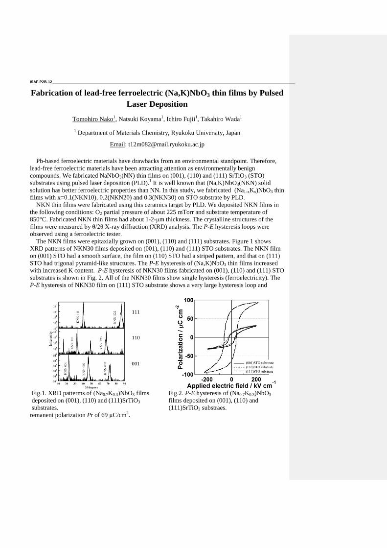
ISAF-P2B-12 ____________________________________________________________________________________________________________________
Fabrication of lead-free ferroelectric (Na,K)NbO3 thin films by Pulsed
Laser Deposition
Tomohiro Nako1, Natsuki Koyama
1, Ichiro Fujii
1, Takahiro Wada
1
1 Department of Materials Chemistry, Ryukoku University, Japan
Email: [email protected]
Pb-based ferroelectric materials have drawbacks from an environmental standpoint. Therefore,
lead-free ferroelectric materials have been attracting attention as environmentally benign
compounds. We fabricated NaNbO3(NN) thin films on (001), (110) and (111) SrTiO3 (STO)
substrates using pulsed laser deposition (PLD).1 It is well known that (Na,K)NbO3(NKN) solid
solution has better ferroelectric properties than NN. In this study, we fabricated (Na1-xKx)NbO3 thin
films with x=0.1(NKN10), 0.2(NKN20) and 0.3(NKN30) on STO substrate by PLD.
NKN thin films were fabricated using this ceramics target by PLD. We deposited NKN films in
the following conditions: O2 partial pressure of about 225 mTorr and substrate temperature of
850°C. Fabricated NKN thin films had about 1-2-μm thickness. The crystalline structures of the
films were measured by θ/2θ X-ray diffraction (XRD) analysis. The P-E hysteresis loops were
observed using a ferroelectric tester.
The NKN films were epitaxially grown on (001), (110) and (111) substrates. Figure 1 shows
XRD patterns of NKN30 films deposited on (001), (110) and (111) STO substrates. The NKN film
on (001) STO had a smooth surface, the film on (110) STO had a striped pattern, and that on (111)
STO had trigonal pyramid-like structures. The P-E hysteresis of (Na,K)NbO3 thin films increased
with increased K content. P-E hysteresis of NKN30 films fabricated on (001), (110) and (111) STO
substrates is shown in Fig. 2. All of the NKN30 films show single hysteresis (ferroelectricity). The
P-E hysteresis of NKN30 film on (111) STO substrate shows a very large hysteresis loop and
remanent polarization Pr of 69 μC/cm2.
111
110
001
Fig.1. XRD patterms of (Na0.7K0.3)NbO3 films
deposited on (001), (110) and (111)SrTiO3
substrates.
Fig.2. P-E hysteresis of (Na0.7K0.3)NbO3
films deposited on (001), (110) and
(111)SrTiO3 substraes.

1 S. Yamazoe, H. Sakurai, M. Fukada, H. Adachi, and T. Wada, Appl. Phys. Lett. , 95, 062906
(2009).

ISAF-P2B-13 ____________________________________________________________________________________________________________________
Effects of InNbO4 fabrication on perovskite PIN-PMN-PT
Linghang Wang1, Zhuo Xu
1
1Electronic Materials Research Laboratory, Key Laboratory of Ministry of
Education&International Center for Dielectric Research, Xi'an Jiaotong University, Xi’an 710049,
P. R. China
Email: [email protected]
Due to the superior piezoelectric properties compared to ceramics and thin films, such as its
ultrahigh piezoelectric coefficients (d33>1500pC/N) and electromechanical coupling factors
(k33>90), the ferroelectric single crystals are regarded as the promising new materials used for
electroacoustic, hydroacoustic or ultrasonic transduction devices. The relaxor-based ferroelectric
ternary Pb(In1/2Nb1/2)O3-Pb(Mg1/3Nb2/3)O3-PbTiO3 (PIN-PMN-PT) crystals have the better
properties at higher temperature, whose Curie temperature is about 200oC with the piezoelectric
constant d33 about 2000pC/N, as compared with the binary Pb(Mg1/3Nb2/3)O3-PbTiO3 (PMN-PT)
single crystals and Pb(In1/2Nb1/2)O3-PbTiO3 (PIN-PT) single crystals for the applications in the high
temperature transduction devices. For PIN-PMN-PT crystal growth, however, the perovskite PIN-
PMN-PT raw materials are very critical. In this paper, we pesented effects of InNbO4 (IN)
fabrication on the perovskite PIN-PMN-PT. Excess of In2O3 and annealing on the phases of
synthesized IN were investigated. The pre-sintered IN and unsintered IN powders on the phases of
PIN-PMN-PT were discussed. The experimental results indicated that excess of In2O3 did not have
influences on the phase of IN due to higher chemical activity of In2O3, IN powder with 3% In2O3
excess was in grey because of the reaction, In2O3→In2O, annealing at 850oC could make grey IN
powder into white. It is apparent that unsintered IN could obtain the pyrochlore-free PIN-PMN-PT
rather than pre-sintered IN powders. An improved way for preparing PIN-PMN-PT raw materials is
developed.
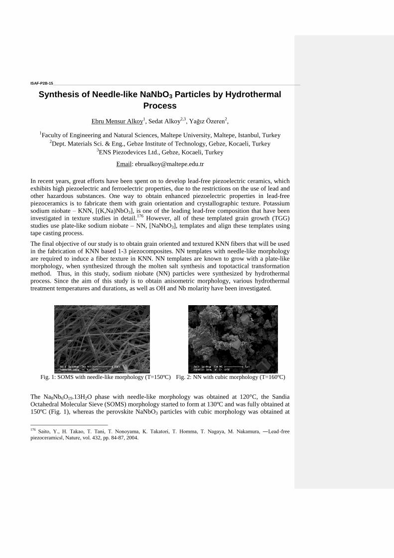
ISAF-P2B-15 ____________________________________________________________________________________________________________________
Synthesis of Needle-like NaNbO3 Particles by Hydrothermal
Process
Ebru Mensur Alkoy1, Sedat Alkoy
2,3, Yağız Özeren
2,
1Faculty of Engineering and Natural Sciences, Maltepe University, Maltepe, Istanbul, Turkey
2Dept. Materials Sci. & Eng., Gebze Institute of Technology, Gebze, Kocaeli, Turkey
3ENS Piezodevices Ltd., Gebze, Kocaeli, Turkey
Email: [email protected]
In recent years, great efforts have been spent on to develop lead-free piezoelectric ceramics, which
exhibits high piezoelectric and ferroelectric properties, due to the restrictions on the use of lead and
other hazardous substances. One way to obtain enhanced piezoelectric properties in lead-free
piezoceramics is to fabricate them with grain orientation and crystallographic texture. Potassium
sodium niobate – KNN, [(K,Na)NbO3], is one of the leading lead-free composition that have been
investigated in texture studies in detail.176
However, all of these templated grain growth (TGG)
studies use plate-like sodium niobate – NN, [NaNbO3], templates and align these templates using
tape casting process.
The final objective of our study is to obtain grain oriented and textured KNN fibers that will be used
in the fabrication of KNN based 1-3 piezocomposites. NN templates with needle-like morphology
are required to induce a fiber texture in KNN. NN templates are known to grow with a plate-like
morphology, when synthesized through the molten salt synthesis and topotactical transformation
method. Thus, in this study, sodium niobate (NN) particles were synthesized by hydrothermal
process. Since the aim of this study is to obtain anisometric morphology, various hydrothermal
treatment temperatures and durations, as well as OH and Nb molarity have been investigated.
The Na8Nb6O19.13H2O phase with needle-like morphology was obtained at 120°C, the Sandia
Octahedral Molecular Sieve (SOMS) morphology started to form at 130ºC and was fully obtained at
150ºC (Fig. 1), whereas the perovskite NaNbO3 particles with cubic morphology was obtained at
176
Saito, Y., H. Takao, T. Tani, T. Nonoyama, K. Takatori, T. Homma, T. Nagaya, M. Nakamura, ―Lead -free
piezoceramics‖, Nature, vol. 432, pp. 84-87, 2004.
Fig. 1: SOMS with needle-like morphology (T=150ºC) Fig. 2: NN with cubic morphology (T=160ºC)

160°C (Fig. 2). Needle-like morphology was retained after annealing at 400-800ºC. The results of
the hydrothermal treatment process will be presented in details.
ISAF-P2B-16 ____________________________________________________________________________________________________________________
Grain oriented (K0.5Na0.5)NbO3-based piezoelectric ceramics prepared
by reactive template grain growth method
A. Hussain1, T. K. Song
1, M. H Kim
1 and W. J. Kim
2
1School of Nano & Advanced Materials Engineering, Chanwon National University, Gyeongnam 641-773,
Republic of Korea
2Department of Physics, Changwon National University, Gyeongnam 641-773, Republic of Korea
Lead-base piezoelectric materials such as Pb(Zr,Ti)O3 (PZT) are widely utilized in electrical devices
because of their excellent properties. However, legislations such as RoHS/WEEE (restriction of hazardous
substances/waste electrical and electronic equipment) demand for the development of lead-free piezoelectric
materials. Lead-free (K, Na)NbO3 (KNN) perovskite system is currently under study as strong potential
candidate for environmentally benign piezoelectric devices. However, pure KNN ceramics are difficult to
sinter by conventional methods, and show inferior properties. To improve the performance of KNN ceramic
system, different techniques for their fabrication such as spark plasma sintering, screen printing, templated
grain growth, and reactive templated growth have been employed. Among these techniques, the reactive
templated grain growth (RTGG) has proved to be more effective in improving the piezoelectric performance.
In this work, lead-free non-stiochiometric (K0.470Na0.545)(Nb0.55Ta0.45)O3 (KNNT) textured ceramics
were prepared by RTGG method using NaNbO3 (NN) templates. The Plate-like NaNbO3 (NN) templates
were synthesized from bismuth layer-structured Bi2.5Na3.5Nb5O18 (BNN) particles by a topochemical
microcrystal conversion (TMC) method. Using 5 wt% of NN templates, textured KNNT ceramics were
fabricated, and their crystal structure, microstructure, dielectric and piezoelectric properties were compared
with non-textured KNNT ceramics prepared by a conventional solid state reaction method. The textured
KNNT ceramics exhibited high grain orientation and high dielectric constant. In addition, piezoelectric
properties of textured KNNT ceramics were improved, giving a high piezoelectric coefficient d33 = 390 pC/N
and piezoelectric coupling coefficient kp = 0.60.
Corresponding author: Ali Hussain
E.mail: [email protected]
ISAF-P2B-17 ____________________________________________________________________________________________________________________
0.6(Bi0.85La0.15)FeO3-0.4PbTiO3 Multiferroic Ceramics by Tape
Casting
JIN Guo-xi, BU Shun-dong, Wang Da-Lei, Dai Rui, CHENG Jin-rong
School of Materials Science and Engineering/Shanghai University, Shanghai/China
Email: [email protected]
For meeting the needs of function-structure integration design in ceramics, new shaping
technology should be applied into modern ceramic materials. In this letter, BFPT-based multiferroic
specimens formed by tape casting method were studied. Firstly, 0.6(Bi0.85La0.15)FeO3-0.4PbTiO3
powders were obtained by solid state reaction calcined at 750oC. Then the powders were mixed
with ethanol, polyvinylbutyral(PVB), dibutyl phthalate(DBP)-polyethylene glycol(PEG) and
Triethylolamine(TEA) to form tape casting slurry with viscosity range from 650 to 2700 mPa.s.
Filming and rheological properties of slurry was studied by adjusting the components content. High
quality casting films were obtained when the ratio of DBP-PEG/PVB was 1.5 with 1% TEA in
slurry. Casting films were dried, cut and laminated into disks. The effects of forming process on
densification and dielectric properties were studied via controlling forming pressure. Ceramics
formed by 200MPa with Tc=410 o
C, tanδ=2.2%, εr=480 at 1kHz while Pr=5.5μC/cm2 at 20kV/cm
were obtained.
ISAF-P2B-18 ____________________________________________________________________________________________________________________
Controllable Synthesis of Different Bismuth Ferrites by an EDTA-assisted Hydrothermal
Method and Photocatalytic Characterization
Tong Tong, Dengren Jin and Jinrong Cheng*
School of materials science and engineering, Shanghai University, Shanghai 200072, P.R.China
*corresponding author: [email protected]
Bismuth ferrites crystallites were synthesized by an EDTA-assisted hydrothermal method using
Fe(NO3)3·9H2O and Bi(NO3)3·5H2O as starting materials with NaOH as the mineralizer. Different
phases of bismuth ferrites including sillenite Bi25FeO40, perovskite BiFeO3 and orthorhombic
Bi2Fe4O9 were obtained respectively in the process of hydrothermal reactions by adjusting the
process parameters, such as NaOH concentration, reaction temperature and duration time et al. The
analysis revealed that EDTA played an important role in the phase evolution of bismuth ferrites and
intensely influenced the morphology of bismuth ferrites powders. The mechanism of forming
different bismuth ferrites in the hydrothermal process was also investigated and discussed.
Moreover, photocatalytic properties of the bismuth ferrites crystallites were explored as well. The
as-prepared powders performed a good degradation effect at visible light region, suggesting their
promising applications as photocatalysts.
Keywords: Bismuth ferrites; Hydrothermal synthesis; EDTA; Photocatalysis
ISAF-P2B-19 ____________________________________________________________________________________________________________________
NANOPARTICLES TRANSPORT IN CERAMIC MATRIXES:
A NOVEL APPROACH FOR CERAMIC MATRIX COMPOSITE FABRICATION
Andrey N. Rybyanets, Anastasia A. Naumenko
Institute of Physics, Southern Federal University
Rostov on Don, Russia
Nanoparticles are perfect building blocks offering a wide variety of compositions, structures and properties, ideally suited to designing functional nanomaterials and nanodevices. Nanoparticles can be embedded in various matrixes; however, a major technological problem is spontaneous aggregation of nanoparticles which, as a result, lose their unique properties. Recently polymer nano- and microgranules filled with nanoparticles (magnetic, metal, oxides etc.) start widely used as a delivery means of nanosubstances in medical, biotechnology and chemical applications. Very recently, there was a tendency to fix (immobilize) particles on the surface of spherical polymeric microgranules. Such composite micro-nano systems offer a number of significant advantages. When fixed to a surface or embedded in microgranules, nanoparticles lose their tendency to readily aggregate but retain their reactivity and, for the most part, their physical properties. Besides, microgranules are easier to manipulate then nanoparticles. Microgranules, coated or filled with nanoparticles can be used to produce “homogeneous” disperse systems, such as sols and aerosols, and fabricate films, coatings or bulk materials.
A novel approaches for fabrication of nano- and microporous piezoceramics as well as ceramic
matrix piezocomposites (CMC’s) are proposed in this work. The technique is based on
nanoparticles transport in ceramic matrixes using polymer nanogranules, coated or filled by a
various chemicals, as a porosifiers at standard ceramics fabrication process. Resulting CMC’s are
composed by super lattices of closed pores filled or coated by nanoparticles of metals, oxides,
ferromagnetics etc., embedded in piezoceramic matrix. Pilot samples of nano and microporous
ceramics and CMC’s were fabricated using different piezoceramics compositions as a ceramic
matrix. Two types of polymer microgranules were used for a nanoparticles transport: polystyrene
microgranules filled by magnetite nanoparticles and polytetrafluoroethylene microgranules coated
by metal nanoparticles. Parent microgranules and nanoparticles as well as resulting CMS’s were
examined using transmission and scanning electron microscopy (TEM and SEM). New family of
nano- and microporous piezoceramics and CMC’s are characterized by a unique spectrum of the
electrophysical properties unachievable for standard PZT ceramic compositions and fabrication
methods, including combination of piezoelectric, magnetic and electrets properties, giant dielectric

relaxation, giant piezoelectric and electrocaloric effects, as well as a possibility of controllable
changes of the main properties within a wide range.
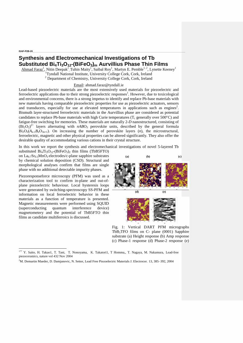
ISAF-P2B-20 ____________________________________________________________________________________________________________________
Synthesis and Electromechanical Investigations of Tb Substituted Bi4Ti3O12-(BiFeO3)m Aurvillius Phase Thin Films
Ahmad Faraz1, Nitin Deepak
1, Tuhin Maity
1, Saibal Roy
1, Martyn E. Pemble
1, 2, Lynette Keeney
1
1Tyndall National Institute, University College Cork, Cork, Ireland
2 Department of Chemistry, University College Cork, Cork, Ireland
Email: [email protected]
Lead-based piezoelectric materials are the most extensively used materials for piezoelectric and
ferroelectric applications due to their strong piezoelectric responses1. However, due to toxicological
and environmental concerns, there is a strong impetus to identify and replace Pb-base materials with
new materials having comparable piezoelectric properties for use as piezoelectric actuators, sensors
and transducers, especially for use at elevated temperatures in applications such as engines2.
Bismuth layer-structured ferroelectric materials in the Aurvillius phase are considered as potential
candidates to replace Pb-base materials with high Curie temperatures (Tc generally over 500C) and
fatigue-free switching for memories. These materials are naturally 2-D nanostructured, consisting of
(Bi2O2)2+
layers alternating with nABO3 perovskite units, described by the general formula
Bi2O2(An-1BnO3n+1). On increasing the number of perovskite layers (n), the microstructural,
ferroelectric, magnetic and other physical properties can be altered significantly. They also offer the
desirable quality of accommodating various cations in their crystal structure.
In this work we report the synthesis and electromechanical investigations of novel 5-layered Tb
substituted Bi4Ti3O12-(BiFeO3)2 thin films (TbB5FTO)
on La0.7Sr0.3MnO3 electrodes/c-plane sapphire substrates
by chemical solution deposition (CSD). Structural and
morphological analyses confirm that films are single
phase with no additional detectable impurity phases.
Piezoresponseforce microscopy (PFM) was used as a
characterization tool to confirm in-plane and out-of-
plane piezoelectric behaviour. Local hysteresis loops
were generated by switching-spectroscopy SS-PFM and
information on local ferroelectric behavior in these
materials as a function of temperature is presented.
Magnetic measurements were performed using SQUID
(superconducting quantum interference device)
magnetometery and the potential of TbB5FTO thin
films as candidate multiferroics is discussed.
177
177
Y. Saito, H. Takao1, T. Tani, T. Nonoyama, K. Takatori1, T Homma,, T. Nagaya, M. Nakamura, Lead-free
piezoceramics, nature vol 432 Nov 2004 2M. Demartin Maeder, D. Damjanovic, N. Setter, Lead Free Piezoelectric Materials J. Electrocer. 13, 385–392, 2004
(a) (b) (c)
(d) (e)
Fig. 1: Vertical DART PFM micrographs
TbB5TFO films on C- plane (0001) Sapphire
substrate (a) Height response (b) Amp response
(c) Phase-1 response (d) Phase-2 response (e)
Frequency tracking response
ISAF-P2B-21 ____________________________________________________________________________________________________________________
Hexagonal Ferrite and Ferroelectric Perovskite Magnetoelectric Composites
Robert C. Pullar*, Marco Medeiros, Dmitry V. Karpinsky and Andrei L. Kholkin
Department of Materials and Ceramic Engineering and CICECO, University of Aveiro, Campus Universitário de Santiago, Aveiro, 3810-193, Portugal
*Presenting author, email: [email protected]
There has been a great deal of interest in the possibility of coupling between magnetic and electrical
properties in multiferroic and magnetoelectric (ME) ceramics. Because of the inherent problems in
establishing good magnetic and dielectric/ferroelectric properties in a single multiferroic material,
we are investigating the manufacture of magnetoelectric composite materials consisting of separate
magnetic and dielectric/ferroelectric ceramic components, and potential coupling between such
components at up to microwave (GHz) frequencies. In this paper we will report our investigations
of composites consisting of the ferrites BaM (BaFe12O19), SrM (SrFe12O19), Co2Z (Ba3Co2Fe24O41)
or SrZ (Sr3Co2Fe24O41) combined with the ferroelectrics BT (BaTiO3) or KN (KNbO3). The ferrites
were produced by various methods – sol-gel, citrate combustion and solid state ceramics – and the
results compared. This is first time such composites have been made with the Z ferrites or
potassium niobate perovskites. The synthesis and properties of the composites were investigated by
XRD, SEM, VSM, PFM/MFM and dielectric measurements.
ISAF-P2B-22 ____________________________________________________________________________________________________________________
Study of polar and electrical properties of Hydroxyapatite:
Modeling and data analysis
Anna Bystrova1, Yuri Dekhtyar
1, Svitlana Kopyl
2, Igor Bdikin
2, Vladimir Bystrov
3, Alla
Sapronova4 and Andrei Kholkin
3
1Insitite of Biomedical Eng. and Nanotechnology, Riga Technical University, Riga, Latvia
2Centre for Mechanical Technology and Automation, University of Aveiro, Aveiro, Portugal
3Department Materials Eng. and Ceramics & CICECO, University of Aveiro, Aveiro, Portugal
4Bergen Center for Computational Science, Unifob AS, N-5008 Bergen, Norway
Email: [email protected]
1. Non-homogeneity of hydroxyapatite (HAP) surface structure was shown by atomic force
microscopy (AFM) with formation of nano-crystals area of ~ 500…1000 nm.
2. These formations could be connected with HAP polymorphism – two phases (hexagonal and
monoclinic) are co-existed, as was shown by our computational modeling (HyperChem 8.0) and
first principles LDA calculations. The unit cell parameters are different for these phases, as results
the area´s height on surface of various phases are altered. This alteration could generate variation of
surface potential, which could be registered by Kelvin probe scanning, and must be create the local
change of work function. It is first reason of local electrical and polar HAP surface peculiarities
influenced on osteoblastes attachment and proliferation.
3. Defects formations (such as oxygen vacancy or hydrogen interstices) change unit cell total
energy and surface potential. Modeling and first principle calculations show that energy
changes/per HAP crystal cell unit are approximately ~ 0.1…0.2 eV for these defects. These changes
coincide with experimentally measured work functions alteration on HAP surface. It must be
second reason for influence of nano-interaction with living cells on the HAP surface.
4. Such defects could be arisen by hydrogenation processes under hydrogen introducing during
high pressure treatment, conjugated with following microwave irradiation. Such insertion could
switch OH dipole orientation and as results change the H-OH ordering along OH-column in HAP
structures and creates non-centrosymmetric polar and piezoelectric local areas on HAP structure
and its surface. This technology was apply now for HAP surface modification and insertion of the
negative electrical charges on the HAP surface layer, that change locally of HAP surface potential
(and consequence its polar properties), which is very influenced on the cell´s adhesion and
proliferation of these living cell, e.g. osteoblasts. Common cumulative effect from reasons 1 and 2
could be estimated by introducing of nano-interaction’s correlation length, which value ~ 200…500
nm correspond to sizes of specific osteoblast’s filaments (such as cell’s leg/stem) and HAP surface
non-homogeneities area.
5. The experimental data of synchrotron illuminations and registered absorption peaks are
investigated and compared with computational estimation of surface potential and work functions
changes under formations of various types of such defects for each HAP crystal phases.
ISAF-P2B-23 ____________________________________________________________________________________________________________________
Effect of B2O3 Addition on Dielectric and Ferroelectric
Properties of BiFeO3 Ceramic
Thanatep Phatungthane, Gobwute Rujijanagul
Department of Physics and Materials Science, Faculty of Sciences, Chiangmai University,
Chiangmai, Thailand
Email: [email protected]
In the present work, the effect of B2O3 addition on sintering behavior, dielectric and
ferroelectric properties of BiFeO3 (BFO) ceramics was investigated. These ceramics were prepared
successfully by a solid state reaction technique for the first time. Phase formations of the obtained
ceramics were investigated by x-ray diffraction technique (XRD). The morphology of the B2O3
added BFO ceramics was characterized by electron microscopy (SEM). The dielectric and
ferroelectric properties of the ceramics were also investigated. Pure phase perovskite was observed.
Our work indicates that the ceramics exhibit good dielectric and ferroelectric behavior.
Acknowledgements
This work was supported by The Royal Golden Jubilee Ph.D. Program, The Thailand
Research Fund (TRF), Faculty of Science and Graduate School Chiang Mai University and National
Research University (NRU), Office of the Higher Education Commission (OCHE) Thailand.
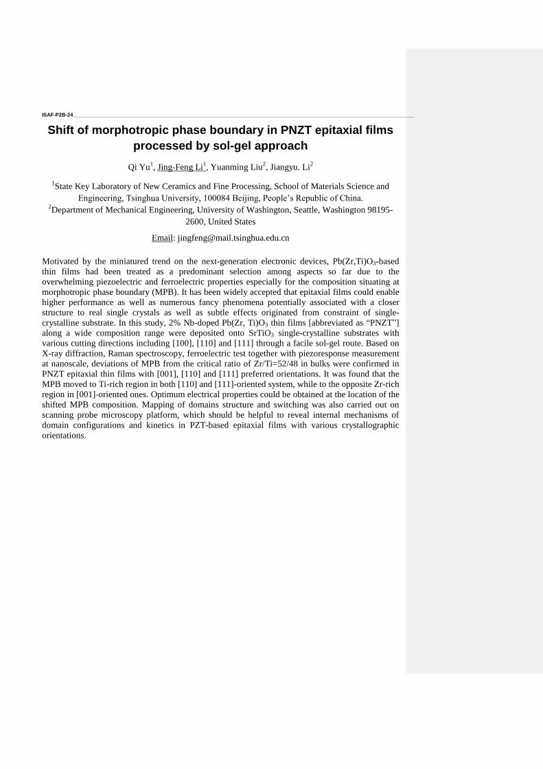
ISAF-P2B-24 ____________________________________________________________________________________________________________________
Shift of morphotropic phase boundary in PNZT epitaxial films
processed by sol-gel approach
Qi Yu1, Jing-Feng Li
1, Yuanming Liu
2, Jiangyu. Li
2
1State Key Laboratory of New Ceramics and Fine Processing, School of Materials Science and
Engineering, Tsinghua University, 100084 Beijing, People’s Republic of China. 2Department of Mechanical Engineering, University of Washington, Seattle, Washington 98195-
2600, United States
Email: [email protected]
Motivated by the miniatured trend on the next-generation electronic devices, Pb(Zr,Ti)O3-based
thin films had been treated as a predominant selection among aspects so far due to the
overwhelming piezoelectric and ferroelectric properties especially for the composition situating at
morphotropic phase boundary (MPB). It has been widely accepted that epitaxial films could enable
higher performance as well as numerous fancy phenomena potentially associated with a closer
structure to real single crystals as well as subtle effects originated from constraint of single-
crystalline substrate. In this study, 2% Nb-doped Pb(Zr, Ti)O3 thin films [abbreviated as “PNZT”]
along a wide composition range were deposited onto SrTiO3 single-crystalline substrates with
various cutting directions including [100], [110] and [111] through a facile sol-gel route. Based on
X-ray diffraction, Raman spectroscopy, ferroelectric test together with piezoresponse measurement
at nanoscale, deviations of MPB from the critical ratio of Zr/Ti=52/48 in bulks were confirmed in
PNZT epitaxial thin films with [001], [110] and [111] preferred orientations. It was found that the
MPB moved to Ti-rich region in both [110] and [111]-oriented system, while to the opposite Zr-rich
region in [001]-oriented ones. Optimum electrical properties could be obtained at the location of the
shifted MPB composition. Mapping of domains structure and switching was also carried out on
scanning probe microscopy platform, which should be helpful to reveal internal mechanisms of
domain configurations and kinetics in PZT-based epitaxial films with various crystallographic
orientations.
Fig. 1: Nanoscale mapping of piezoresponse phase configuration of PNZT epitaxial films (Zr/Ti=30/70, 001-
oriented).
ISAF-P2B-25 ____________________________________________________________________________________________________________________
Microstructure and Optical Properties of Er2O3 - Doped
Potassium Sodium Niobate-Tellurite Glass-ceramics
P. Yongsiri1, and K. Pengpat
1,2
1 Department of Physics and Materials Science, Faculty of Science,
Chiang Mai University, Chiang Mai, 50200, Thailand 2 Materials Science Research Center, Faculty of Science, Chiang Mai, 50200, Thailand
Email: [email protected]
Ferroelectric glass-ceramics have been extensively studied as they possesses the properties of non-
porous glasses as well as ferroelectric crystals, giving rise to materials that have the good
mechanical properties of glass and the electro-optical properties of ferroelectric crystals. In this
work, ferroelectric potassium sodium niobate [(K0.5Na0.5)NbO3 or KNN] crystals are of interest
because of their distinct electrical properties1 and non-linear optical properties
2. Many researchers
have attempted to produce glass-ceramics with the ferroelectric178
KNN phase3-4
. The difficult part
of preparing this glass type is to crystallize the KNN single phase. The idea of combining potassium
sodium niobate crystals in some selected glasses has therefore been developed and called the
incorporation method5. In the present study, KNN crystals were firstly introduced to tellurite base
glasses. Transparent glasses of erbium oxide (Er2O3)-doped KNN-tellurite glasses were then
successfully prepared by using the incorporation method. Experiments started with the preparation
of KNN powder by simple mixed oxide method using calcination temperature of 900oC for 5 h.
Then, the calcined KNN powder was mixed with TeO2 and 0.5-1 mol% Er2O3 dopant. Each batch
was subsequently melted at 800oC for 15 min in a platinum crucible using an electric furnace. The
quenched glasses were then subjected to heat treatment at various temperatures for 4 h in order to
form glass-ceramics with the desired crystal phases. X-ray diffraction (XRD) results showed that
KNN solid solution distributed over the glass-ceramic samples. Scanning electron microscopy
(SEM) revealed that nano-crystals of KNN and some secondary crystals precipitated in the glass-
ceramics. Crystal sizes increased with increasing heat treatment temperatures. The optical and
physical properties of the prepared glass-ceramics were measured. The values of refractive index
(n) ranged between 1.99 and 2.15, while that of density (ρ) ranged between 4.70-5.18 g/cm3. Energy
band gap from the transmission cut-off wavelength (Eg) was measured as 3.14-3.20 eV.
178
M. Ichiki, L. Zhang, M. Tanaka and R. Maeda, “Electrical properties of piezoelectric sodium-potassium
niobate”, J. Eur. Ceram. Soc., Vol. 24, Issue 6, p. 1693–1697, 2004. 2 A. Aronne, E. Fanelli, P. Pernice, S. Peli, C. Giannetti and G. Ferrini, “Crystallization and second harmonic
generation in potassium–sodium niobiosilicate glasses”, J. Solid State Chem., Vol. 182, p. 2796–2800, 2009. 3 A. Aronne, E. Fanelli, P. Pernice, S. Peli, C. Giannetti and G. Ferrini, “Crystallization and second harmonic
generation in potassium–sodium niobiosilicate glasses”, J. Solid State Chem., Vol. 182, p. 2796–2800, 2009. 4 D. E. Vernacotola, S. Chatlani, J. E. Shelby, “Ferroelectric sodium-potassium-niobium silicate glass ceramics”,
proceedings of the 2000 12th IEEE international symposium on application of ferroelectrics, Vol. 2, p. 829, 2000. 5 P. Yongsiri, S. Eitssayeam, G. Rujijanagul, S. Sirisoonthorn, T. Tunkasiri and K. Pengpat, “Fabrication of transparent
lead-free KNN glass-ceramics by incorporation method”, Nanoscale. Res. Lett., Vol. 7, p. 136, 2012.

ISAF-P2B-26 ____________________________________________________________________________________________________________________
Sputtered Pb(Zr,Ti)O3 piezoelectric films for MEMS application
Hiroki Kobayashi1, Mitsunori Henmi
1, Mitsutaka Hirose
1, Isao Kimura
1, Takehito Jinbo
1,
Koukou Suu1
1 Institute of Semiconductor and Electronics Technologies, ULVAC Inc.,
1220-1 Suyama Susono, Shizuoka, Japan
Email: [email protected]
One of the difficulties in PZT film deposition by sputtering method is to keep the stability in the
lead content which is volatile element and deposition rate with the passage of sputtering time.
Another would be how to obtain higher piezoelectric coefficient e31 of PZT film for high-
performance devices such as sensor and actuator. In this work, some key technologies for
perovskite oxide thin-film production including production tool technologies, their performances of
sputtering, and improvement of properties of PZT film will be introduced.
A multi-chamber type mass production sputtering systems for electronic devices SME-200E
(ULVAC Inc.) equipped with an exclusive sputtering module was used. When insulating PZT film
adhered to the shields of the ground potential, charge-up occurred, the impedance of the system
changed, plasma was pushed to the center of the chamber, exposure to plasma was enhanced, and as
a consequence, Pb content within film reduced. In order to stabilize the status of plasma, we
installed a stable anode, that is, an anode that avoided charge-up due to the adhesion of insulating
PZT film and maintained the role as an anode [1]. As a result that a stable anode was installed, the
change in the Pb composition was 1.0±0.6% by the evaluation until end of target life (total wafer;
400 pieces @2 µm thickness PZT). And the change in the deposition rate was 3.8 μm/h±1.4% and
uniformity of within wafer was less than ±5% by the evaluation until end of target life. As a result
that a stable anode was installed, stability of Pb content and deposition rate within film in
continuous sputtering has been confirmed.
PZT films have been deposited on 8inch diameter Pt(111)/TiOX/SiO2/Si substrates. The PZT films
were deposited under Ar/O2 mixed gas atmosphere of 0.5 Pa. Substrate temperature was heated up
to around 580°C. PZT films were deposited with relatively high growth rate about 3.8 μm/h and
these thicknesses was 2.0 μm. PZT film oriented PZT(001)/(100) preferably, and the pyrochlore
phase cannot be detected. We also note that post in-situ treatment [2] has been recently established,
aiming to improve crystalline property and piezoelectric coefficient in our PZT films. After in-situ
treatment, piezoelectric coefficient e31 increased up to -19.2 C/m2, which is remarkably improved
compared to e31 of -14.7 C/m2 as deposited. We have established both mass production capability
and advanced process capability for MEMS devices.
[1] United States Patent, US 6,521,105 B2 (2003)
[2] Kobayashi et.al in preparation
ISAF-P2B-27 ____________________________________________________________________________________________________________________
Structural, ferroelectric and piezoelectric properties
of composition spread Bi1-xGaxFeO3 thin films
N. Jaber1, J. Wolfman
1, C. Daumont
1, B. Négulescu
1, A. Ruyter
1, G. Feuillard
1, J. Fortineau
1,
T. Sauvage2, B. Courtois
2, C. Autret-Lambert
1, F.Gervais
1
1 GREMAN laboratory, UMR7347 CNRS, Université François Rabelais, Tours, France
2 CEMHTI laboratory, UPR3079 CNRS, Orléans, France
Email: [email protected]
The coexistence in some oxide materials of distinct ferroic orders (ferroelectricity,
ferromagnetism, ferroelasticity) open the way to new multifunctional applications. Among those
materials, PZT [(PbZrO3)1-x(PbTiO3)x] and PMNPT [(PbMg1/3Nb2/3O3)1-x(PbTiO3)x] solid solutions
exhibit the highest ferroelectric-ferroelastic coupling and are widely used as piezoelectric sensors or
more recently for energy harvesting applications. However lead-based compound are about to be
banished by European RoHS regulation and a lead-free replacement is required. An important
piezoelectric effect has recently been shown in Bi1-xRexFeO3 (Re : rare earth) thin films solid
solutions1, related with the occurrence of a morphotropic phase boundary (MPB), as it is the case
for PZT and PMNPT. In this work, we report the exploration of Bi1-xGaxFeO3 (BGFO) phase
diagrams. Composition spread epitaxial BGFO thin films were grown by pulsed laser deposition
onto La0.8Sr0.2MnO3 electrodes. Composition gradients were characterized by EDX and RBS while
phase analysis was realized by X-Ray micro-diffraction (XRMD). Impedance spectroscopy,
ferroelectric cycles and XRMD versus temperature were used to identify phase transitions and
MPBs locations in the composition spread films. Cartographies of the effective d33 measured at
various length scales with PFM (a few nm), laser interferometry (a few m) and XRMD (a few 100
m) across composition spread will be presented and compared.
ISAF-P2B-28 ____________________________________________________________________________________________________________________
Magnetoelectric Coupling of Pb(Zr0.52Ti0.48)O3/Pt/CuFe2O4
Multilayer Thin Films
Sung-Ok Hwang1, Chang Young Koo
1, You Jeong Eum
1, Jungho Ryu
2, Hee Young Lee
1,*
1School of Materials Science and Engineering, Yeungnam University,
Gyeongsan, 712-749, Korea 2Functional Ceramics Research Group, Korea Institute of Materials Science (KIMS),
Gyeongnam, 641-831, Korea
*Email: [email protected]
The multiferroic materials and/or multilayer structure of ferroelectric/ferromagnetic materials can be used for sensors, memory storage devices, energy harvesting devices and so on due to their magnetoelectric(M-E) coupling properties . But single-phase multiferroic materials such as BFO(BiFeO3) still have shown lower M-E coupling properties than multilayer structured ones. Therefore, the hybrid structured ferroelectric/magnetic materials have received a great deal of attention because their high M-E performances, but it’s also still restricted to bulk materials. In this regards, we have prepared multilayer thin film structure with PZT and Cu-ferrite.
Polycrystalline Pb(Zr0.52Ti0.48)O3(PZT)/Pt/CuFe2O4 multilayer thin films on quarts(or SiO2/Si) substrate. The film structure is tri-layered type, CuFe2O4 film was deposited by using pulsed laser deposition (PLD) method. In order to investigate annealing effect on film microstructure, ferroelectric and ferromagnetic properties of multilayer thin films, CuFe2O4 layer was heat-treated at various temperatures. For measuring their electrical and magnetoelectric properties, Pt electrode layer was deposited on the CuFe2O4 layers by sputtering. PZT layers were fabricated by sol-gel method on Pt interlayer. And Pt top electrodes were also deposited using by sputtering with shadow mask. Structural and microstructural properties of PZT/Pt/CuFe2O4 multilayer thin films were observed by XRD and SEM. Ferroelectric and ferromagnetic behaviors of multilayer films were examined by measuring polarization and magnetization – electric and magnetic field hysteresis. Magnetoelectric coefficients were calculated by measured magnetoelectric voltages using magnetoelectric measurement system.
We’ll discuss the annealing effect on ferroelectric and ferromagnetic properties of multilayer films, and also discuss the M-E coupling properties as a function of annealing temperatures in detail.
ISAF-P2B-29 ____________________________________________________________________________________________________________________
Microstructure and kHz- and GHz- Range Dielectric properties
of Polycrystalline Ba0.5Sr0.5TiO3 Thin Films
Tanja Pečnik1,2
, Sebastjan Glinšek3,4
, Brigita Kmet1,4
, Barbara Malič1,2,4
1Electronic Ceramics Department, Jožef Stefan Institute, Jamova cesta 39, 1000 Ljubljana, Slovenia
2Jožef Stefan International Postgraduate School, Jamova cesta 39, 1000 Ljubljana, Slovenia
3School of Engineering, Brown University, 184 Hope Street, Providence, Rhode Island 02912, USA
4Centre of Excellence SPACE-SI, Aškerčeva cesta 12, 1000 Ljubljana, Slovenia
Email: [email protected]
The BaxSr1-xTiO3 (x=0–1) solid solution is suitable for tunable microwave applications, such as
phase shifters, tunable resonators, etc. Its main advantage is composition-tunable functional
response, i.e., high dielectric permittivity, relatively low dielectric losses and high tunability at
microwave frequencies179
. In the case of solution-derived thin films, knowledge and control of the
microstructure-dielectric properties relations is of crucial importance for the integration into
devices. In this contribution we present the processing of Ba0.5Sr0.5TiO3 (BST) thin films on
polycrystalline alumina substrates and the study of the relationships between the microstructure and
the RF- and MW-range dielectric properties in these films.
The 0.25 M solutions were prepared via alkoxides-based route from alkaline earth acetates and Ti-
butoxide, which were dissolved in the 2-methoxyethanol-acetic acid mixture. The precursor
solutions were spin-coated on the alumina substrates and the as-deposited films were dried at
200 °C, pyrolyzed at 350 °C and annealed in a rapid thermal annealing furnace at 900 °C. The
deposition-annealing steps were repeated several times to achieve the final thickness of the films.
According to the XRD analysis, the films crystallize in the randomly oriented perovskite phase. The
SEM analysis revealed uniform in-plane microstructures, with grains of a few 10 nm and about 100
nm in 170 nm- and 500 nm- thick films, respectively.
For the RF-range dielectric characterization the planar capacitor structures were deposited using the
lift-off photolithography, while the split-post dielectric resonators were used for MW
measurements. The about 170 nm thick films reached the values of the dielectric permittivity,
dielectric losses and tunability (ε0V/ε40V) of 994, 0.01 and 1.63, measured at 100 kHz. The dielectric
properties of the films with different thicknesses, from about 100 nm to 600 nm, and
microstructures, will be presented in the contribution.
179
M. J. Lancaster, “Thin-film ferroelectric microwave devices”, Supercond. Sci. Technol, vol. 11, p. 1323-1334, 1998.

ISAF-P2B-30 ____________________________________________________________________________________________________________________
Effects of Thermal Treatment on the Properties of Zirconium
Doped Barium Titanate Ceramics
Parkpoom Jarupoom1, Anocha Munpakdee
2, Sukum Eitssayeam
3, Kamonpan Pengpat
3,
Pongthep Arkornsakul3, Gobwute Rujijanagul
3
1Department of Industrial Engineering, Faculty of Engineering, Rajamangala University of
Technology Lanna (RMUTL), Chiang Mai, 50300, Thailand 2General Science Department, Faculty of Science, Srinakharinwirot University,
Bangkok, 10110, Thailand 3Department of Physics and Materials Science, Faculty of Science, Chiang Mai University, Chiang
Mai, 50200, Thailand
Email: [email protected]
In this work, zirconium doped barium titanate ceramics were prepared via a solid state technique.
After sintering at 1,450
C for 2h, the ceramics were annealed at 1,200 C for 4-16 h. Effects of the
thermal treatment on the electrical properties of the ceramics was investigated. An improvement in
strain level, ferroelectric properties and piezoelectric coefficient were observed for the 8 h sample.
High strain level and calculated d33 (d*33) of 0.26% and 326 pm/V were also obtained for this
sample. The electrical properties were found to correlate with the densification and second phase
formation.
Acknowledgement: The authors would like to thank the Graduate School of Srinakharinwirot
University.
ISAF-P2B-31 ____________________________________________________________________________________________________________________
Electrical Properties of (1-x)BCZT-xBZT Lead-Free Ceramics
Piewpan Parjansri1, Sukum Eitssayeam
1,2
1Department of Physics and Materials Science, Faculty of Science, Chiang Mai University,
Chiang Mai 50200, Thailand 2Materials Science Research Center, Faculty of Science, Chiang Mai 50200, Thailand
Email: [email protected]
The aim of this study was to investigate the electrical properties of (1-x)[Ba0.85Ca0.15Zr0.1 Ti0.9]O3-
x[(BiZn0.5Ti0.5)O3] ceramics system for x = 0.00-0.10. The (1-x)BCZT-xBZT ceramics were
fabricated via solid state reaction technique. The samples were calcined and sintered at 925 ºC for 6
h and 1370 ºC for 3 h, respectively. Phase formation and microstructure of (1-x)BCZT-xBZT
ceramics were studied using an X-ray diffractometer (XRD) and scanning electron microscope
(SEM). The physical properties and electrical properties, such as dielectric properties and
ferroelectric properties were examined. It was found that all the samples show pure perovskite
phase. Grain size and density value were in the range of 2.18-13.30 m and 5.61-5.77 g/cm3,
respectively. The BZT content lead to the change and improved of the dielectric properties of
ceramic samples. The dielectric loss values were lower than 0.01 (at 1 kHz) for all samples. The
samples show higher degree of the relaxor like behavior with higher BZT content. In addition, the
ferroelectric properties were found to depend on the BZT content.
ISAF-P2B-32 ____________________________________________________________________________________________________________________
Relationship of Microstructure and Electrical Properties in Sol-
Gel PZT Films
Konstantin Vorotilov1, Alexander Sigov
1, Dmitry Seregin
1, Yury Podgorny
1, Olga Zhigalina
2,
Dmitry Khmelenin2
1Moscow State Technical University of Radioengineering, Electronics and Automation (MIREA),
Moscow, Russia 2Shubnikov Institute of Crystallography, Russian Academy of Sciences, Moscow, Russia
Email: [email protected]
Thin PZT films are a prominent material for ferroelectric random access memory (FRAM), MEMS
and other integrated ferroelectric devices180
.
Despite the fact that formation of perovskite phase in PZT films prepared by sol-gel techniques has
been the subject of investigation since 1990s, mechanisms of fine crystalline structure formation,
nucleation and growth processes are as yet not fully understood. A comparison between results
reported by different authors is complicated due to various precursor chemistry and preparation
conditions. A comprehensive discussion of different approaches to sol-gel synthesis of PZT films
and nucleation processes was made recently in refs.181,182
.
In this work we try to establish main regular trends in formation of fine crystalline structure (with
the use of TEM techniques) of sol-gel PZT thin films annealed at different temperatures and its
effect on electrical properties of the films.
For this purpose in addition to the range of annealing temperatures Ta = 600 - 750°C commonly
used for preparation of sol-gel PZT films, we have studied both the film annealed at low
temperature Ta = 550°C, where perovskite phase has not completely arisen, and one annealed at
high temperature Ta = 900°C, that leads to degradation of multilevel heterostructure as a result of
diffusion processes.
The structure of the films was studied by transmission electron microscopy (TEM), electron and X-
ray diffraction; electrical properties were characterized by Sawyer-Tower, capacitance-voltage and
current-voltage techniques.
Experimental data on film microstructure (grain size, texture, pyrochlore inclusions, interfaces),
changes in structure and composition of the underlying layers are discussed in association with
electrical properties of the films.
180
N. Setter, D. Damjanovic, L. Eng, et al. “Ferroelectric thin films: Review of materials, properties, and applications”,
J. Appl. Phys., vol. 100, p. 051606, 2006. 181
T. Schneller, and R. Waser, “Chemical modifications of Pb(Zr0.3,Ti0.7)O3 precursor solutions and their influence on
the morphological and electrical properties of the resulting thin films”, J. Sol-Gel Sci. Techn., vol. 42, p. 337-352, 2007. 182
A. C. Dippel, T. Schneller, R. Waser, D. Park, and J. Mayer, “Formation sequence of lead platinum interfacial
phases in chemical solution deposition derived Pb(Zr1-x Ti x)O3 thin films”, Chem. Mater., vol. 22, p. 6209 – 6211,
2010.

ISAF-P2B-33 ____________________________________________________________________________________________________________________
Fabrication and Characterization of PZT-PAni/PVDF Based
Nanocomposite
Oliveira Cibele1, Fuzari Jr, Gilberto de C.
3, Sakamoto, Walter
2.,Longo Elson
1, Zaghete, Maria A.
1.
1 Depto de Bioquímica e Tecnologia Química, Instituto de Química/ Univ.
Estadual Paulista – UNESP, Araraquara, S P/ Brasil 2 Depto de Física e Química, Faculdade de Engenharia/ Univ. Estadual Paulista -
UNESP , Ilha Solteira, S P/Brasil 3 Instituto de Ciências Exatas e da Terra (ICET)/ Univ. Federal de Mato Grosso-
UFMT/ Barra do Garças, MT – Brasil
Email: [email protected]
This work presents the preparation and characterization of PZT ceramic obtained by different
methods. The influence of the synthesis method on the grain size and the morphology are also
object of study. The fabrication and characterization of composite films with 0-3 connectivity,
immersing nanoparticles of PZT into the non-polar poly(vinylidene fluoride) – PVDF as the
polymer matrix were presented. For comparison there are results obtained with composite samples
made of ceramic particles unrecovered and recovered with a conducting polymer. In this sample the
PZT grain was partially covered by PAni, which allowed better distribution of grains in the polymer
matrix avoiding a continuous electrical flux path which does not allow the polarization process of
the composite sample. The use of this composite as sensor and power converter is an indicative that
it is a good alternative for technological applications. The concept of energy harvesting must be
related to capture the ambient energy and convert it into usable electrical energy without
environment attack i.e., a clean electric energy. Although there are a number of sources of
harvestable ambient energy, such as solar energy and energy from wind, piezoelectric materials are
very interesting due to their ability to convert applied strain energy into usable electric energy1. For
material to be used as a sensor, the relationship between output voltage and input power should be
linear, i.e., the responsivity should remain constant. And regarding the magnitude of responsivity, it
may indicate the quality of the sensor, i.e. the larger the magnitude, more input signal is being
converted into output signal. Samples of PZT/PVDF 30/70 vol.% without and with PAni (PZT-
PAni/PVDF), previously polarized with a electric field of 5 MV/m for 15 min were characterized. A
analysis of the results allows observing that the composite with polyaniline (PAni) was superior in
all respects in comparison to the other composite. It can easily be observed when comparing the two
composites 30/70 vol.% that PZT-PAni/PVDF presents better results2.
Fig.1. FE-SEM images of composite
PZT – Pani / PVDF with PZT
nanostructures synthesized by
(a) Pechini method (b) hydrothermal
microwave method
ISAF-P2B-34 ____________________________________________________________________________________________________________________
Ultrathin BaTiO3/Fe bilayer obtained by Atomic Layer
Deposition for magnetoelectric devices
E. Martinez-Guerra1, Paul P. Horley
1
1 Centro de Investigación en Materiales Avanzados (CIMAV S.C.), Chihuahua/Monterrey, 31109
Chihuahua, México.
Email: [email protected]
Ferroelectric ultrathin BaTiO3 (BTO) films in contact with Fe underlayer have been grown by
Atomic Layer Deposition (ALD) on silicon substrates. In this work Ba-Ti-O films were deposited at
380 °C using Ba cyclopentadienyl precursors and titanium alkoxides. Binary reactions of
Ba(tBu3C5H2)2 and H2O are first studied separately in BaO deposition and are found to result in a
hydration/dehydration cycle, which is strongly influenced by temperature. Self-limiting growth of
amorphous barium titanate films becomes possible when Ti(OMe)4–H2O growth cycles are mixed
as well as possible with Ba( t Bu3C5H2)2–H2O cycles. The formation of Ba(OH)2 is an issue for
deposition of Ba-containing materials with H2O as the oxygen source, and can be severe at low
temperatures. The high growth rates up to 1.0 Å/cycle in this preliminary study were most likely
due to a surface hydroxide contribution to the film growth and thermal decomposition of Ti(OiPr)4.
A strong influence of water purging time was found in growth at 235 °C. The addition of titanium
methoxide–water cycles is effective in stopping a BaO/(Ba(OH)2(H2O)n hydration/dehydration
cycle and thus makes self-limiting growth of Ba–Ti–O films possible. Even though fairly uniform
films could be grown with fixed precursor pulse lengths and sufficiently long H2O purge times, the
required H2O purge time was seen to increase with longer Ba(tBu3C5H2)2 pulses, resulting in nearly
doubled growth rates in the 1–5 second pulse and purge timescale often used in practical ALD. Low
temperature ALD of barium-containing oxides with H2O can thus be both difficult and time
consuming. The situation was improved considerably in higher temperature processing with
Ti(OMe)4 as the titanium source, and self-limiting conditions were found. In general it can be
assumed that Ba-Ti-O growth with H2O as the oxygen source becomes easier with lower Ba content
in the film and with as high as possible process temperature, as long as precursor self-
decomposition is avoided. The as-deposited amorphous films are crystallized by post-deposition
annealing at 700 °C. Once the BTO films were crystallized Fe films were prepared by DC-Ion
Sputtering on Si/BTO substrates. Fe films were patterned to form bands by using a shadow mask.
The magnetoelectric effect (ME) was measured with a variation of magnetic field up to 366.07
kA/m and superimposed by a modulation magnetic field of 0.80 kA/m. These magnetic fields were
supplied by an electromagnet with a modula-ted Helmholz coil and the voltage was detected by a
lock-in amplifier. The ME coefficient was calculated as a variation of the electric field in response
to the applied magnetic field. The effect of the modulation frequency was studied by making ME
measurements at 7 different frequencies from 400 to 1000 Hz. We also study theoretically the
multiferroic dynamics in a composite one-dimensional system consisting of BaTiO3 multiferroically
coupled to an iron chain1. These theoretical results are useful to describe multiferroic interaction at
the interface.

1 Paul P. Horley, “Influence of magnetoelectric coupling on electric field induced magnetization reversal in a composite unstrained multiferroic chain”, PHYSICAL REVIEW B 85, 054401 (2012).
ISAF-P2B-35 ____________________________________________________________________________________________________________________
Preparation and Energy Storage Properties of Barium
Strontium Titanate Glass-Ceramic Composites via a Sol Coated
Method
Qingyuan Hu1, Xiaoyong Wei
1, Li Jin
1
1Electronic Materials Research Laboratory, Key Laboratory of the Ministry of Education and
International Center for Dielectric Research, Xi’an Jiaotong University, Xi’an 710049, China
Email: [email protected]
The Ba0.6Sr0.4TiO3 based glass-ceramics was successfully fabricated by a sol coated process. In this
process, the nanosized Ba0.6Sr0.4TiO3 (abbreviated as BST) powders prepared by sol-gel technology
were dispersed into the MgO-SiO2 glass-sol. The influence of the glass content on the
microstructure, dielectric, and energy storage properties of this BST based glass-ceramics has been
investigated. It is found that the grain size and dielectric constant of such glass-ceramics decreased
with the increasing glass concentration. The average breakdown strength of samples with 4% by
weight of glass additive increased dramatically, which was about 1.5 times higher than pure BST.
The energy storage density was also studied, showing that the BST based glass-ceramics prepared
by this sol coated method has a potential for pulse power applications.
ISAF-P2B-36 ____________________________________________________________________________________________________________________
Fabrication and characterization of Pb0.3Sr0.7TiO3 thin films on stainless steel by the Sol-gel method
Shengli Huang and Jinrong Cheng
School of Materials Science and Engineering, Shanghai University, Shanghai, 200072, China
Email:[email protected]
Abstract:
Pb0.3Sr0.7TiO3 (PST) thin films were deposited on La0.5Sr0.5CoO3 (LSCO)-buffered stainless steel (SS)
substrates. Both PST and LSCO thin films were prepared by the sol-gel method. X-ray diffraction
and scanning electron microscopy analysis were used to investigate the crystallinity and surface
morphology of PST thin films. It showed that the crack-free PST thin films presented pure
perovskite phase.The introduction of LSCO had been found to facilitate the formation of (100)
textured PST thin films. The dielectric loss and tunability of the PST thin films measured at 1MHz
were 0.018 and 0.32 respectively. The figure of merit (FOM) of PST thin films reached a maximal
value of 18.2. These measured properties indicate that the PST thin film is a promising candidate
for tunability devices.
Keywords: PST thin films, Sol-gel method, Stainless Steel, dielectric properties, tunability
ISAF-P2B-37 ____________________________________________________________________________________________________________________
Synthesis, Microstructural and Electrical Characterization of
ZnO Nanorods Arrays Films with Different Diameter for
Nanogenerators
Natiara V Madalossi1, Anderson V. Martins, Fernando A. Sigoli
2, Ítalo O. Mazali
2
1DMI, Centre for Information Technology Renato Archer - CTI, Campinas/Brazil
2Funtional Materials Laboratory, Chemistry Institute / Universidade Estadual de Campinas,
Campinas, SP/Brazil
Email: [email protected]
Harvesting of unexploited mechanical energy to power and drive electronic or nanodevices is
increasingly attracting scientific attention.1 Nanoscale materials and nanotechnology could play
important roles in the development of very small volume nanogenerators for self-powder electronics
and nanodevices.2-5
The 1 D ZnO nanostructures have been studied as nanogenarators due to
excellent semiconducting and piezoelectric
properties; little toxicity which makes it good for
biosafe, biocompatible biomedical applications.
In this work, ZnO nanorods were synthesized by
chemical bath deposition (CBD).
Initially, a zinc citrate solution with viscosity
range from 40 to 100 cP was deposited on
Pt/Ti/SiO2/Si substrates by spin coating and heat
treatment at 500 °C by 30 min, 550 °C by 4 h and
700 °C by 2 h to be used as nucleation layer.
After that, the nanorods were synthesized by
CBD at 110oC by using zinc acetate and KOH
with concentration 0.033 mol L-1 as
precursors. The ZnO nanorods were characterized
by XRD and FE-SEM as structural and
microstructural properties. A series of oriented hexagonal wurtzite ZnO nanorods array films
were grown on Pt/Ti/SiO2/Si substrates. The effect of the nucleation layer on the structure and
and diameter of ZnO nanorod array film was analyzed. It was found that the viscosity and heat
treatment of the zinc citrate solution influenced on the diameter and length of the nanorods. A
simple method was used for characterize the output voltage of the nanorods arrays films with
different diameter. It was used a device with 8 mm2 and Pt/Ti/SiO2/Si as counter electrode. It was
observed that the device show a Schottky behavior from I vs V curves. The voltage measured
ranged from 2 mV to 7 mV.
1 R. S. Devan, R. A. Patil, J. Lin and Y. Ma, “One-dimensional Metal-Oxide Nanostructures: Recent Developments in
Synthesis, Characterization and Applications”, Materials Views, Vol. 22, pp. 3326 -3370, 2012.
2P. X. Gao, J. H. Song and Z. L. Wang, Advanced Materials, Vol. 19, pp. 67-72, 2007.
3 X. D. Wang, J. H. Song, J. Liu, Z. L. Wang, Science, Vol 316, pp. 102-105, 2007.
4 M. P. Lu, J. Song, M. Y. Lu, M. T. Chen, Y. Gao, L. J. Chen, Z. L. Wang, NanoLetteres, Vol. 9, PP. 1223-1224, 2009.
Fig. 48: ZnO nanorods array film and output
voltage.
0 5 10 15 20 25-8,0x10
-3
-6,0x10⁻³
-4,0x10⁻³
-2,0x10⁻³
0,0
2,0x10⁻³
4,0x10⁻³
6,0x10⁻³
8,0x10⁻³
Time (s )
Vo
lta
ge
(V )

5 R. Yang, Y. Quin, C. Li, G. Zhu, Z. L. Wang, Nano Letters, Vol. 92, PP. 1201-1205, 2009.
ISAF-P2B-38 ____________________________________________________________________________________________________________________
Multiferroic bismuth ferrite based thin films
G. Yesner, R. Rivera, L. Klein, A. Safari
Glenn Howatt Electroceramic Laboratory, Department of Materials Science and Engineering,
Rutgers University, Piscataway, New Jersey
Email: [email protected]
BiFeO3 (BFO) has stimulated a great interest in recent years for its multiferroic behavior and
high remnant polarization at room temperature. However, high leakage current resulting from
oxygen vacancies limits the practical applications of BFO films. Therefore, manganese doping is
used in order to reduce leakage current. Mn-doped BFO thin films are deposited on Pt/TiO2/SiO2/Si
substrate by a sol gel technique and compared with the un-doped BFO thin films.
A stoichiometric 0.2M BFO precursor solution was prepared followed by a modified sol gel
and spin coating route. The nitrate raw materials were dissolved in a combination of ethylene glycol
and citric acid followed by heating. Layers were deposited on the Pt/TiO2/SiO2/Si substrate and
dried on a hot plate. Additional layers were deposited and dried to achieve the desired thickness of
the film. Finally, the film was annealed using rapid thermal annealing (RTA). A similar process was
carried out to fabricate Mn-doped BFO thin films.
The phase, microstructural, and electrical properties were investigated. The un-doped
BFO sample (200nm) has unsaturated polarization with 2Ps = 80.4 µC.cm-2
, 2Pr = 33.0µC.cm-2
, and
2Ec = 400kV.cm-1
. For the Mn-doped thin films, the leakage current is reduced by two orders of
magnitude compared to un-doped samples. It is observed that the remnant polarization increases
from 16.5 to 40µC.cm-2
. Processing will be further refined in order to improve electrical properties.
ISAF-P2B-39 ____________________________________________________________________________________________________________________
The effect of substitution on the synthesis and dielectric
properties of lead-free KNN ceramics
Ilze Smeltere, Maija Antonova, Anna Kalvane, Maris Livinsh
Institute of Solid State Physics University of Latvia
Email: [email protected]
Potassium sodium niobate (KNN) solid solutions are considered as possible alternative for the
widely used PZT in some applications. However it is difficult to sinter fully dense KNN ceramic
body what restricts the electrical properties. Therefore modification of ceramics has been
performed: MnO2 was used as a sintering aid and partial B-site ion substitution was made. Obtained
ceramics have a single phase of perovskite structure. The sintering process of alkaline niobates is
characterized by forming a liquid phase which enhanced density of ceramics. For undoped KNN
ceramic two sharp phase transitions are observed at 190o and about 410
oC, corresponding to the
phase transitions from orthorhombic to tetragonal (TO-T) and from ferroelectric tetragonal to
paraelectric cubic (Tc), respectively. After the partial substitution for Nb+5
both of these phase
transitions are shifted to lower temperatures while increasing dielectric permittivity ε.
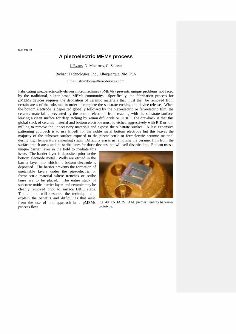
ISAF-P2B-40 ____________________________________________________________________________________________________________________
A piezoelectric MEMs process
J. Evans, N. Montross, G. Salazar
Radiant Technologies, Inc., Albuquerque, NM USA
Email: [email protected]
Fabricating piezoelectrically-driven micromachines (pMEMs) presents unique problems not faced
by the traditional, silicon-based MEMs community. Specifically, the fabrication process for
pMEMs devices requires the deposition of ceramic materials that must then be removed from
certain areas of the substrate in order to complete the substrate etching and device release. When
the bottom electrode is deposited globally followed by the piezoelectric or ferroelectric film, the
ceramic material is prevented by the bottom electrode from reacting with the substrate surface,
leaving a clean surface for deep etching by xenon difluoride or DRIE. The drawback is that this
global stack of ceramic material and bottom electrode must be etched aggressively with RIE or ion-
milling to remove the unnecessary materials and expose the substrate surface. A less expensive
patterning approach is to use lift-off for the noble metal bottom electrode but this leaves the
majority of the substrate surface exposed to the piezoelectric or ferroelectric ceramic material
during high temperature annealing steps. Difficulty arises in removing the ceramic film from the
surface trench areas and the scribe lanes for those devices that will self-disarticulate. Radiant uses a
unique barrier layer in the field to mediate this
issue. The barrier layer is deposited prior to the
bottom electrode metal. Wells are etched in the
barrier layer into which the bottom electrode is
deposited. The barrier prevents the formation of
unetchable layers under the piezoelectric or
ferroelectric material where trenches or scribe
lanes are to be placed. The entire stack of
substrate oxide, barrier layer, and ceramic may be
cleanly removed prior to surface DRIE steps.
The authors will describe the technique and
explain the benefits and difficulties that arise
from the use of this approach in a pMEMs
process flow.
Fig. 49: ENHARVKAAL picowatt energy harvester
prototype.
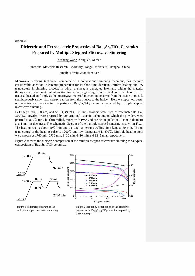
ISAF-P2B-41 ____________________________________________________________________________________________________________________
Dielectric and Ferroelectric Properties of Ba1-xSrxTiO3 Ceramics
Prepared by Multiple Stepped Microwave Sintering
Xusheng Wang, Yang Yu, Xi Yao
Functional Materials Research Laboratory, Tongji University, Shanghai, China
Email: [email protected]
Microwave sintering technique, compared with conventional sintering technique, has received
considerable attention in ceramic preparation for its short time duration, uniform heating and low
temperature in sintering process, in which the heat is generated internally within the material
through microwave-material interaction instead of originating from external sources. Therefore, the
material heated uniformly as the microwave-material interaction occurred from the inside to outside
simultaneously rather than energy transfer from the outside to the inside. Here we report our result
on dielectric and ferroelectric properties of Ba1-xSrxTiO3 ceramics prepared by multiple stepped
microwave sintering.
BaTiO3 (99.9%, 100 nm) and SrTiO3 (99.9%, 100 nm) powders were used as raw materials. Ba1-
xSrxTiO3 powders were prepared by conventional ceramic technique, in which the powders were
prefired at 800℃ for 2 h. Then milled, mixed with PVA and pressed to pellet of 10 mm in diameter
and 1 mm in thickness. The schematic diagram of the multiple stepped sintering is sown in Fig.1.
The heating rate is about 10℃/min and the total sintering dwelling time kept to 60 min. The up
temperature of the heating pulse is 1200℃ and low temperature is 800℃. Multiple heating steps
were chosen as 1*60 min, 2*30 min, 3*20 min, 6*10 min and 12*5 min, respectively.
Figure 2 showed the dielectric comparison of the multiple stepped microwave sintering for a typical
composition of Ba0.9Sr0.1TiO3 ceramics.
60 min
20C
1200C
1*60 min
30min30min
800C
1200C
20C2*30 min
Figure 1 Schematic diagram of the
multiple stepped microwave sintering
Figure 2 Frequency dependence of the dielectric
properties for Ba0.9Sr0.1TiO3 ceramics prepared by
different steps
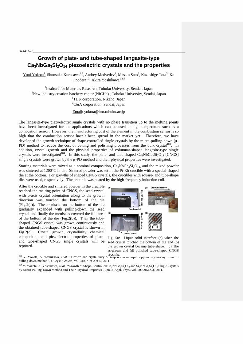
ISAF-P2B-42 ____________________________________________________________________________________________________________________
Growth of plate- and tube-shaped langasite-type
Ca3NbGa3Si2O14 piezoelectric crystals and the properties
Yuui Yokota1, Shunsuke Kurosawa
1,2, Andrey Medvedev
1, Masato Sato
3, Kazushige Tota
3, Ko
Onodera1,3
, Akira Yoshikawa1,2,4
1Institure for Materials Research, Tohoku University, Sendai, Japan
2New industry creation hatchery center (NICHe) , Tohoku University, Sendai, Japan
3TDK corporation, Nikaho, Japan
4C&A corporation, Sendai, Japan
Email: [email protected]
The langasite-type piezoelectric single crystals with no phase transition up to the melting points
have been investigated for the applications which can be used at high temperature such as a
combustion sensor. However, the manufacturing cost of the element in the combustion sensor is so
high that the combustion sensor hasn’t been spread in the market yet. Therefore, we have
developed the growth technique of shape-controlled single crystals by the micro-pulling-down (-
PD) method to reduce the cost of cutting and polishing processes from the bulk crystal183
. In
addition, crystal growth and the physical properties of columnar-shaped langasite-type single
crystals were investigated184
. In this study, the plate- and tube-shaped Ca3NbGa3Si2O14 [CNGS]
single crystals were grown by the -PD method and their physical properties were investigated.
Starting materials were mixed as a nominal composition, Ca3NbGa3Si2O14, and the mixed powder
was sintered at 1200°C in air. Sintered powder was set in the Pt-Rh crucible with a special-shaped
die at the bottom. For growths of shaped CNGS crystals, the crucibles with square- and tube-shape
dies were used, respectively. The crucible was heated by the high-frequency induction coil.
After the crucible and sintered powder in the crucible
reached the melting point of CNGS, the seed crystal
with a-axis crystal orientation along to the growth
direction was touched the bottom of the die
(Fig.2(a)). The meniscus on the bottom of the die
gradually expanded with pulling-down the seed
crystal and finally the meniscus covered the full-area
of the bottom of the die (Fig.2(b)). Then the tube-
shaped CNGS crystal was grown continuously and
the obtained tube-shaped CNGS crystal is shown in
Fig.2(c). Crystal growth, crystallinity, chemical
composition and piezoelectric properties of plate-
and tube-shaped CNGS single crystals will be
reported.
183
Y. Yokota, A. Yoshikawa, et.al., “Growth and crystallinity of shaped and multiple sapphire crystals by a micro-
pulling-down method”, J. Cryst. Growth, vol. 318, p. 983-986, 2011. 184
Y. Yokota, A. Yoshikawa, et.al., “Growth of Shape-Controlled Ca3NbGa3Si2O14 and Sr3NbGa3Si2O14 Single Crystals
by Micro-Pulling-Down Method and Their Physical Properties”, Jpn. J. Appl. Phys., vol. 50, 09ND03, 2011.
Fig. 50: Liquid-solid interface (a) when the
seed crystal touched the bottom of die and (b)
the grown crystal became tube-shape. (c) The
as-grown and (d) polished tube-shaped CNGS
crystals.
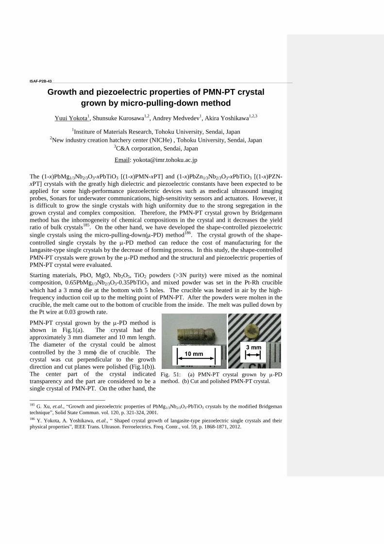
ISAF-P2B-43 ____________________________________________________________________________________________________________________
Growth and piezoelectric properties of PMN-PT crystal
grown by micro-pulling-down method
Yuui Yokota1, Shunsuke Kurosawa
1,2, Andrey Medvedev
1, Akira Yoshikawa
1,2,3
1Institure of Materials Research, Tohoku University, Sendai, Japan
2New industry creation hatchery center (NICHe) , Tohoku University, Sendai, Japan
3C&A corporation, Sendai, Japan
Email: [email protected]
The (1-x)PbMg1/3Nb2/3O3-xPbTiO3 [(1-x)PMN-xPT] and (1-x)PbZn1/3Nb2/3O3-xPbTiO3 [(1-x)PZN-
xPT] crystals with the greatly high dielectric and piezoelectric constants have been expected to be
applied for some high-performance piezoelectric devices such as medical ultrasound imaging
probes, Sonars for underwater communications, high-sensitivity sensors and actuators. However, it
is difficult to grow the single crystals with high uniformity due to the strong segregation in the
grown crystal and complex composition. Therefore, the PMN-PT crystal grown by Bridgemann
method has the inhomogeneity of chemical compositions in the crystal and it decreases the yield
ratio of bulk crystals185
. On the other hand, we have developed the shape-controlled piezoelectric
single crystals using the micro-pulling-down(-PD) method186
. The crystal growth of the shape-
controlled single crystals by the -PD method can reduce the cost of manufacturing for the
langasite-type single crystals by the decrease of forming process. In this study, the shape-controlled
PMN-PT crystals were grown by the -PD method and the structural and piezoelectric properties of
PMN-PT crystal were evaluated.
Starting materials, PbO, MgO, Nb2O5, TiO2 powders (>3N purity) were mixed as the nominal
composition, 0.65PbMg1/3Nb2/3O3-0.35PbTiO3 and mixed powder was set in the Pt-Rh crucible
which had a 3 mm die at the bottom with 5 holes. The crucible was heated in air by the high-
frequency induction coil up to the melting point of PMN-PT. After the powders were molten in the
crucible, the melt came out to the bottom of crucible from the inside. The melt was pulled down by
the Pt wire at 0.03 growth rate.
PMN-PT crystal grown by the -PD method is
shown in Fig.1(a). The crystal had the
approximately 3 mm diameter and 10 mm length.
The diameter of the crystal could be almost
controlled by the 3 mm die of crucible. The
crystal was cut perpendicular to the growth
direction and cut planes were polished (Fig.1(b)).
The center part of the crystal indicated
transparency and the part are considered to be a
single crystal of PMN-PT. On the other hand, the
185
G. Xu, et.al., “Growth and piezoelectric properties of PbMg1/3Nb2/3O3-PbTiO3 crystals by the modified Bridgeman
technique”, Solid State Commun. vol. 120, p. 321-324, 2001. 186
Y. Yokota, A. Yoshikawa, et.al., “ Shaped crystal growth of langasite-type piezoelectric single crystals and their
physical properties”, IEEE Trans. Ultrason. Ferroelectrics. Freq. Contr., vol. 59, p. 1868-1871, 2012.
Fig. 51: (a) PMN-PT crystal grown by -PD
method. (b) Cut and polished PMN-PT crystal.

periphery part had no transparency and the result is due to the evaporation of PbO during crystal
growth. Other crystal growth and properties of grown crystals will be reported.
ISAF-P2B-44 ____________________________________________________________________________________________________________________
Electromechanical displacement of soft/hard PZT bi-layer
composite actuator
Piyalak Ngernchuklin1, C. Jeerapan
1, C. Eamchotchawalit
1
1 Materials Innovation, Thailand institute of scientific and technological research (TISTR),
Klong Luang, Pathum Thani, 12120, Thailand
Email: [email protected]
Lead Zirconate Titanate (PZT) is a well-known piezoelectric material which has been widely used
for transducer, sensor and actuator applications. According to the compositional modifications near
morphotropic phase boundary, PZTs can be classified into two types, soft PZT and hard PZT,
which are distinguished by the piezoelectric properties. Therefore, the combination effect of the
strain-E-field response of soft/hard PZT composite actuator has been much interested to be
observed. In this study, soft and hard PZT powders were co-pressed into bi-layer disks with various
ratios of soft PZT powder, ranging from 0-100 vol. % (with 10 % increments) and then co-sintering.
Due to the shrinkage rate difference of the two layers, the bi-layer composites with various dome
heights were obtained. Moreover, it was shown that the constrained layer either soft PZT or hard
PZT affected to the dome geometry, the strain-E-field response and displacement hysteresis loop.
The electromechanical properties and actuation performance of such bi-layer composite actuators
have been investigated and compared to the soft and hard PZT single layer counterparts.
Keywords : soft PZT, hard PZT, bi-layer composite, actuator
ISAF-P2B-45 ____________________________________________________________________________________________________________________
Polyol-based synthesis of high quality lead zirconate titanate nanostructured thin films
A.Nourmohammadi1, M. Khosravi
2, E. Bahremandi
3*
1 Department of Nanothechnology, Faculty of Advanced Science and Technologies, University of Isfahan, 81746-
73441, Isfahan, I. R. Iran 2 Department of Nanothechnology, Facuity of Advanced Science and Technologies, University of Isfahan, 81746 -
73441, Isfahan, I. R. Iran 3 Department of Physics, Islamic Azad University, Central Tehran Branch, 14837-69444, Tehran, I.R. Iran
Email: [email protected]
*Email:[email protected]
Nanostructured piezoelectric oxide thin films are suitable two-dimensional materials for the
fabrication of many functional nanodevices such as nanosensors, nanoactuators and nano-
electromechanical systems (NEMS). Lead zirconate titanate (PZT), with the perovskite structure, is
a suitable ferroelectric and piezoelectric ceramic material for these applications because it has high
spontaneous polarization, dielectric permittivity and piezoelectric coefficients. Therefore, much
effort has already been devoted to improve the quality of PZT thin films.
PZT thin films have already been synthesized by the alkoxide based sol–gel technique using the
hydrolysis and condensation of these precursors. However, alkoxide-based PZT sols are almost
unstable because they contain water which lowers their storage time. This prevents longtime storage
of the prepared PZT sols. Besides, successful crystallization of the perovskite phase from the
annealed alkoxide-based PZT gels requires heat treatment above 650°C which alters the PbO
stoichiometry of the film due to evaporation.
Here, high quality single phase PZT thin films were synthesized via a polyol-based sol–gel process.
It was shown that single perovskite phase PZT thin films can be effectively produced using the
polyol-based PZT sols at 590°C. Polyol-based process is a cost-effective synthesis method for the
fabrication of PZT thin films because chloride precursors of titanium and zirconium are used. In
addition, polyol-based sols are highly stable for a very long time of storage. However, this process
is not extensively investigated, and only one report is available on the successful fabrication of PZT
thin films using this methodxxiii
.
The prepared PZT thin films were deposited on Au/SiO2
substrates to fabricate high quality PZT thin films. The
films were built up with multiple spin-coating. Each
coating step was followed by pyrolysis at 450°C, and the
produced multilayered thin film was annealed at 590°C.
X-ray diffraction, XRD, investigations confirmed
formation of perovskite PZT thin films. Scanning
electron microscopy, SEM, investigations indicated that
high quality and crack free thin films have been obtained
(Fig 1).
1Q.Zou" Novel polyol-derived sol route for fabrication of PZT thin ferroelectric films" Mat. Lett. 40(1999)240-245.
Fig1.SEM micrograph of a PZT thin film.
ISAF-P2B-46 ____________________________________________________________________________________________________________________
UV laser-induced poling inhibition in proton exchanged
optical waveguides in lithium niobate
G. Zisis1, M. Manzo
2, K. Gallo
2, T. Limböck
3, E. Soergel
3, S. Mailis
1
1Optoelectronics Research Centre, University of Southampton, Southampton, SO17 1BJ, U.K.
2KTH, Applied Physics, SE-106 91 Stockholm, Sweden
3Institute of Physics, University of Bonn, Wegelerstrasse 8, 53115 Bonn, Germany
Email: [email protected]
UV laser irradiation of the +z polar face of congruent and MgO doped lithium niobate crystals has
been observed to inhibit ferroelectric domain inversion when the crystal subsequently undergoes
uniform electric field poling at room temperature.187
The UV laser-induced poling inhibition (PI)
produces ferroelectric domain structures, which correspond to the UV laser-irradiated tracks and
which have sufficient depth (a few m) to overlap with waveguide modes.188
A common procedure
for the fabrication of optical waveguides in lithium niobate is proton exchange followed by an
annealing step.189
Such waveguides are known as
annealed proton exchanged (APE) waveguides.
Here we report preliminary results, which show
that PI is applicable to APE wave-guides thus
enabling the use of this method for the production
of nonlinear optical waveguide devices. We
therefore utilized a graded-index APE waveguide
with a 1/e-depth of ~ 2.2m.
The existence of PI domains in the APE
waveguides was given by piezoresponse force
microscopy (PFM). Further evidence for the
presence of PI domains in this material system
were provided by wedge polishing at an oblique
angle (~ 5 degrees) with respect to the surface,
followed by brief etching in an HF acid solution.
Wedge polishing offers in addition a detailed
view of the depth profile because of a x10
stretching factor which corresponds to a slope of
5°.
187
C. L. Sones, A. C. Muir, Y. J. Ying, S. Mailis, R. W. Eason, T. Jungk, A. Hoffmann, E. Soergel, "Precision
nanoscale domain engineering of lithium niobate via UV laser induced inhibition of poling" Appl. Phys. Lett., vol. 92,
072905, 2008. 188
H. Steigerwald, M. Lilienblum, F. von Cube, Y. J. Ying, R. W. Eason, S. Mailis, B. Sturman, E. Soergel, K. Buse,
"Origin of UV-induced poling inhibition in lithium niobate crystals" Phys. Rev. B, vol. 82, p. 214105, 2010 189
K. Gallo, C. B. E. Gawith, I. T. Wellington, S. Mailis, R. W. Eason, P. G. R. Smith, D. J. Richardson, and S. M.
Kostritskii, “UV-written channel waveguides in proton-exchanged LiNbO3”, J. Appl. Phys., vol. 101, 14110, 2007
Fig. 52: PFM scan of a PI domain obtained on an
APE waveguide. The sample was wedge-polished.
Image size: 30µm x 30µm

The ability to obtain PI domain structures in proton exchanged waveguides in lithium niobate opens
the way for the utilization of this method for the fabrication of nonlinear, electro-optic and acousto-
optic devices in lithium niobate.
ISAF-P2B-47 ____________________________________________________________________________________________________________________
Adsorption Controlled MOCVD Growth of Bismuth Ferrite Thin Films
Nitin Deepak1,2
, Lynette Keeney1, Martyn E. Pemble
1,2 and Roger W. Whatmore
1,2
1Tyndall National Institute, University College Cork, ‘Lee Maltings’, Dyke Parade, Cork, Ireland
2Department of Chemistry, University College Cork, Dyke Parade, Cork, Ireland
Email: [email protected]
Bismuth ferrite (BiFeO3) is one of the most widely studied materials due to its interesting
multiferroic properties1. The growth of BiFeO3 by chemical vapour deposition (CVD) proves to be
a unique challenge due to the interesting chemistry that happens during the growth. The growth
window regarding temperature, pressure and precursor flow rates for pure BiFeO3 phase is very
small2, making the controlled growth of BiFeO3 rather difficult.
In this present work we studied the metalorganic CVD (MOCVD) growth of epitaxial BiFeO3 thin
films on SrTiO3 substrates and found that by carefully controlling the amount of the iron precursor,
Fe(thd)3, where thd = 2,2,6,6 tetramethyl 3,5 heptanedionate, we were able to achieve adsorption
controlled growth. Adsorption controlled growth of BiFeO3 has been previously achieved using
molecular beam epitaxy (MBE)3 but to the best of our knowledge our work represents the first
example of adsorption controlled growth of BiFeO3 by MOCVD. The effect of the volume of the
precursor injected on the growth of BiFeO3 thin films is studied. Detailed x-ray diffraction (XRD)
and transmission electron microscopy (TEM) studies are presented.
References:
1. J. Wang, J. B. Neaton, H. Zheng, V. Nagarajan, S. B. Ogale, B. Liu, D. Viehland, V.
Vaithyanathan, D. G. Schlom, U. V. Waghmare, N. A. Spaldin, K. M. Rabe, M. Wuttig and
R. Ramesh, Science 299, 1719 (2003).
2. S. Y. Yang, F. Zavaliche, L. Mohaddes-Ardabili, V. Vaithyanathan, D. G. Schlom, Y. J.
Lee, Y. H. Chu, M. P. Cruz, Q. Zhan, T. Zhao and R. Ramesh, Applied Physics. Letters 87,
102903 (2005).
3. J. F. Ihlefeld, A. Kumar, V. Gopalan, D. G. Schlom, Y. B. Chen, X. Q. Pan, T. Heeg, J.
Schubert, X. Ke, P. Schiffer, J. Orenstein, L. W. Martin, Y. H. Chu and R. Ramesh, Applied
Physics Letters 91, 071922 (2007).
ISAF-P2B-48 ____________________________________________________________________________________________________________________
Functional properties of lead-free perovskite
(Na0.5Bi0.5TiO3)1-x - (BaTiO3)x thin films
N. D. Scarisoreanu1, F. Craciun
2, A. Andrei
1, R. Birjega
1, C. Galassi
3, M. Dinescu
1.
1NILPRP, Bucharest, Romania
2CNR-Istituto dei Sistemi Complessi, Rome, Italy
3CNR-ISTEC, Faenza, Italy
Email: [email protected]
The solid solution of (Na0.5Bi0.5TiO3)1-x - (BaTiO3)x is considered to be among the best candidate
lead-free ferroelectric and piezoelectric material for applications as actuators and nonvolatile
memory devices. The lead-free perovskite (Na0.5Bi0.5TiO3)1-x - (BaTiO3)x (NBT-BT) has a
morphotropic phase boundary (MPB) between the rhombohedral and tetragonal phase (x =0.06 -
0.07), for which the dielectric, piezoelectric and ferroelectric properties of the material are
considerably enhanced.
In this study, we have investigated the role of the BT amount on the crystalline structure,
microstructure, dielectric properties, phase transition temperatures and stability limits of
ferroelectric phases in NBT-BT thin films grown by pulsed laser deposition. Successful growth of
NBT-BT films on platinized silicon substrates has been achieved, the dielectric and piezoelectric
properties of the films being comparable with bulk values. For example, the NBT-BT (x=-0.06) thin
films show a classic switching behavior, the locally measured value of effective piezoelectric
coefficient d33 eff
was 83 pm/V, which is higher than the previously reported values for pure NBT or
several (more used) lead-based thin films. An enhanced stability of ferroelectric phase in thin films
with respect to bulk has been observed and explained by their peculiar microstructure.
ISAF-P2B-49 ____________________________________________________________________________________________________________________
Effects of TiO2 addition on microstructure and dielectric
properties of phase-mixed BST ceramics
Lixin Zhou, Dengren Jin, Jinrong Cheng, Hanting Dong, Chaojun Xie
(School of Materials Science and Engineering,Shanghai University,200072)
Abstract: The effects of TiO2 addition on dielectric temperature stability of the phase-mixed BST
ceramics were investigated. These non-uniform phase-mixed BST ceramics were synthesized by a
modified solid-state reaction. TiO2 was introduced by the following ways: the TiO2 powders were
mixed with BT and ST powders (MixTi), and the TiO2 were proportionally introduced during the
calcining of BT and ST powders respectively (CalTi). The phase structures and microstructures of
these ceramics were characterized by XRD and SEM, respectively. The compositional gradients
were also examined by EDS and XRD. The Curie peak of MixTi is the lowest and widest, and
MixTi has the best temperature stability, but the normol phase-mixed BST has much higher and
more narrow Curie peak. MixTi also have high tunability more than 30%(1kV/mm, 100kHz). When
TiO2 was introduced during the calcination of ST, the BST has high and narrow Curie peak, and the
temperature stability becomes worse. The surface SEM micrographs of these ceramics exhibite that,
the grain size of MixTi is obviously smaller than the normol phase-mixed BST. In conclusion, the
addition of TiO2 can improve the thermal stability of BST, and sintering routine, such as sintering
temperature and holding duration can change the properties of the Ti-excess BST. MixTi has better
temperature stability, one reason probably is that TiO2 can defer the diffusion of Ba2+ and Sr2+, and
their compositional gradients is maintained, and the grain size may be another cause. Different
properties by various ways of TiO2 addition may be mainly caused by the region of Ti-excess. Ti-
excess region may exist at the grain boundary of BT, while most Ti-excess region may grow in the
grain of ST. The mechanism of TiO2 addition’s effects on the temperatures stability and
microstructures of the phase-mixed BST were investigated, respectively.
Key words: Ti-excess, (Ba,Sr)TiO3, phase-mixed, dielectric properties, temperature stability,
microwave tunable
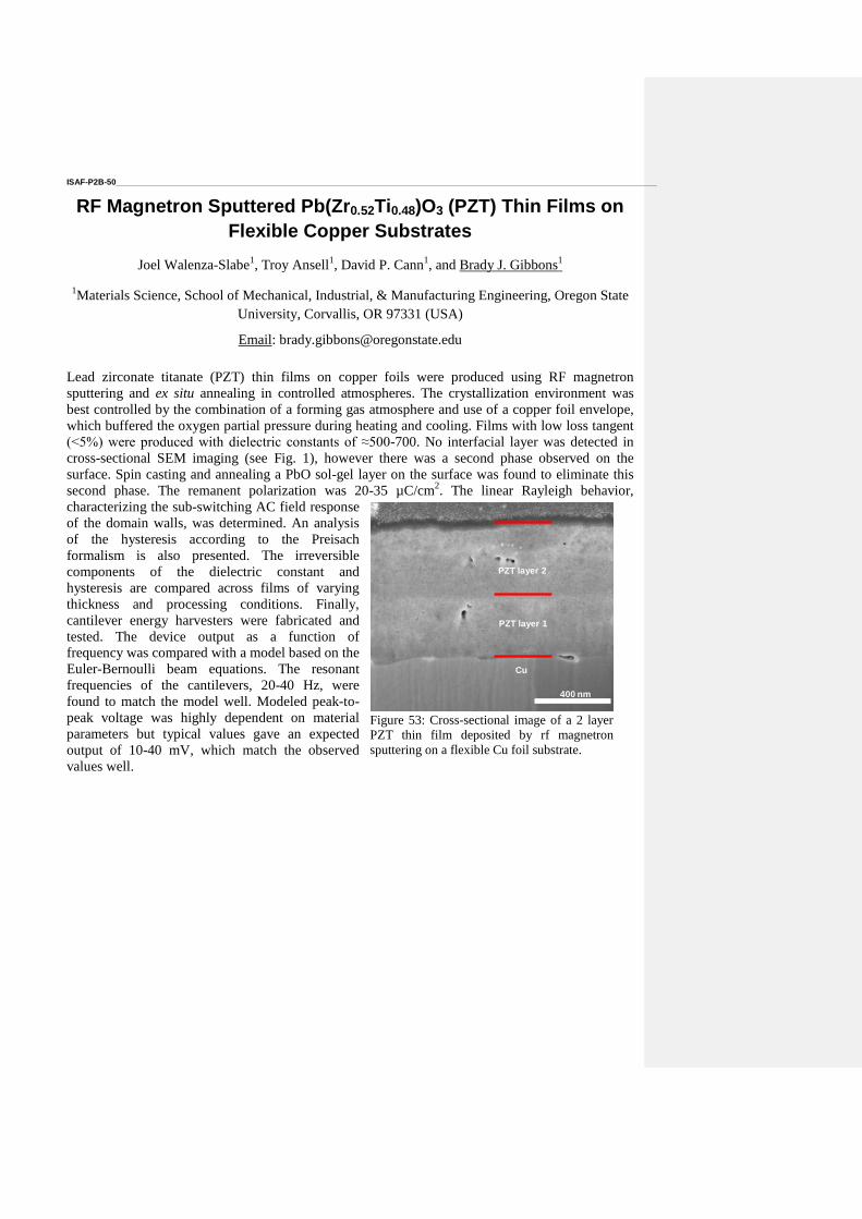
ISAF-P2B-50 ____________________________________________________________________________________________________________________
RF Magnetron Sputtered Pb(Zr0.52Ti0.48)O3 (PZT) Thin Films on
Flexible Copper Substrates
Joel Walenza-Slabe1, Troy Ansell
1, David P. Cann
1, and Brady J. Gibbons
1
1Materials Science, School of Mechanical, Industrial, & Manufacturing Engineering, Oregon State
University, Corvallis, OR 97331 (USA)
Email: [email protected]
Lead zirconate titanate (PZT) thin films on copper foils were produced using RF magnetron
sputtering and ex situ annealing in controlled atmospheres. The crystallization environment was
best controlled by the combination of a forming gas atmosphere and use of a copper foil envelope,
which buffered the oxygen partial pressure during heating and cooling. Films with low loss tangent
(<5%) were produced with dielectric constants of ≈500-700. No interfacial layer was detected in
cross-sectional SEM imaging (see Fig. 1), however there was a second phase observed on the
surface. Spin casting and annealing a PbO sol-gel layer on the surface was found to eliminate this
second phase. The remanent polarization was 20-35 µC/cm2. The linear Rayleigh behavior,
characterizing the sub-switching AC field response
of the domain walls, was determined. An analysis
of the hysteresis according to the Preisach
formalism is also presented. The irreversible
components of the dielectric constant and
hysteresis are compared across films of varying
thickness and processing conditions. Finally,
cantilever energy harvesters were fabricated and
tested. The device output as a function of
frequency was compared with a model based on the
Euler-Bernoulli beam equations. The resonant
frequencies of the cantilevers, 20-40 Hz, were
found to match the model well. Modeled peak-to-
peak voltage was highly dependent on material
parameters but typical values gave an expected
output of 10-40 mV, which match the observed
values well.
PZT layer 2
PZT layer 1
Cu
400 nm
Figure 53: Cross-sectional image of a 2 layer
PZT thin film deposited by rf magnetron
sputtering on a flexible Cu foil substrate.
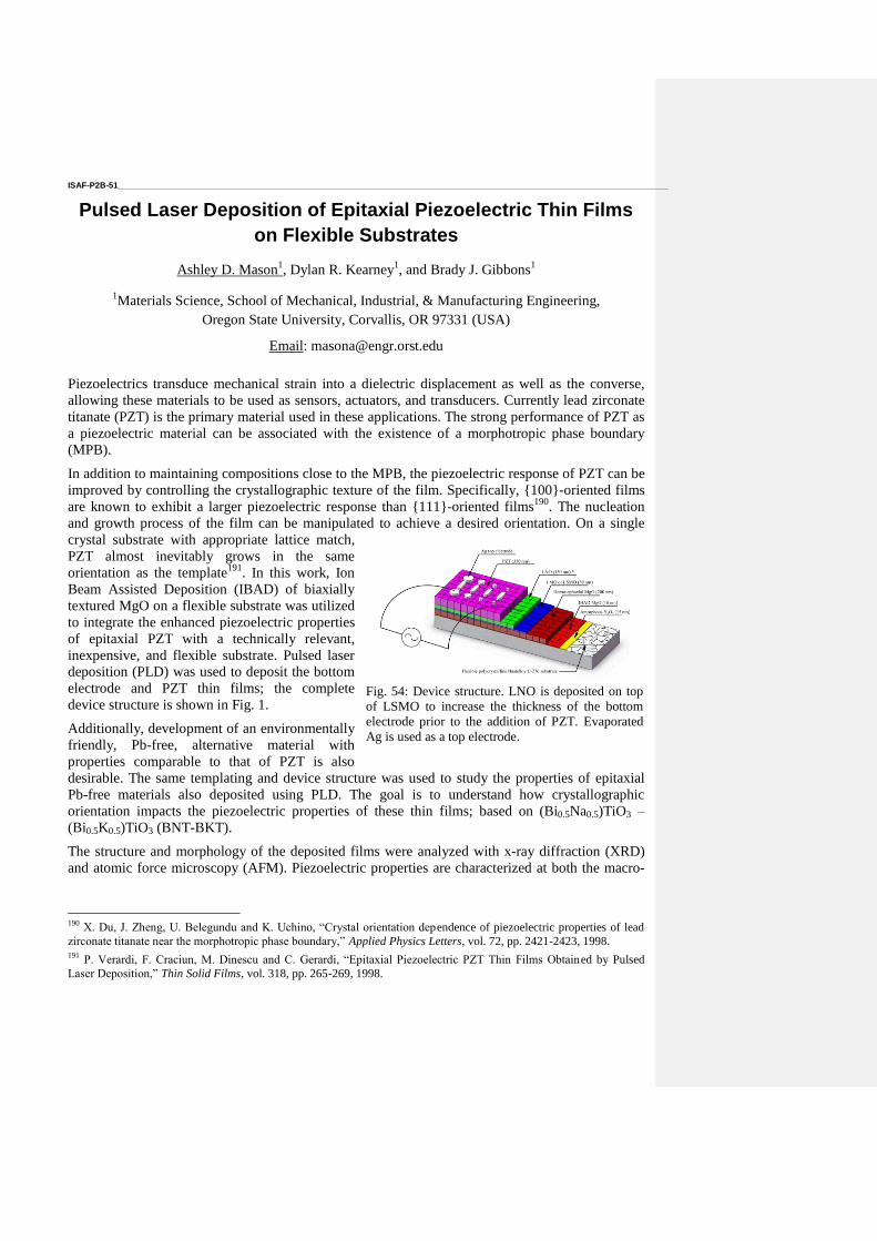
ISAF-P2B-51 ____________________________________________________________________________________________________________________
Pulsed Laser Deposition of Epitaxial Piezoelectric Thin Films
on Flexible Substrates
Ashley D. Mason1, Dylan R. Kearney
1, and Brady J. Gibbons
1
1Materials Science, School of Mechanical, Industrial, & Manufacturing Engineering,
Oregon State University, Corvallis, OR 97331 (USA)
Email: [email protected]
Piezoelectrics transduce mechanical strain into a dielectric displacement as well as the converse,
allowing these materials to be used as sensors, actuators, and transducers. Currently lead zirconate
titanate (PZT) is the primary material used in these applications. The strong performance of PZT as
a piezoelectric material can be associated with the existence of a morphotropic phase boundary
(MPB).
In addition to maintaining compositions close to the MPB, the piezoelectric response of PZT can be
improved by controlling the crystallographic texture of the film. Specifically, {100}-oriented films
are known to exhibit a larger piezoelectric response than {111}-oriented films190
. The nucleation
and growth process of the film can be manipulated to achieve a desired orientation. On a single
crystal substrate with appropriate lattice match,
PZT almost inevitably grows in the same
orientation as the template191
. In this work, Ion
Beam Assisted Deposition (IBAD) of biaxially
textured MgO on a flexible substrate was utilized
to integrate the enhanced piezoelectric properties
of epitaxial PZT with a technically relevant,
inexpensive, and flexible substrate. Pulsed laser
deposition (PLD) was used to deposit the bottom
electrode and PZT thin films; the complete
device structure is shown in Fig. 1.
Additionally, development of an environmentally
friendly, Pb-free, alternative material with
properties comparable to that of PZT is also
desirable. The same templating and device structure was used to study the properties of epitaxial
Pb-free materials also deposited using PLD. The goal is to understand how crystallographic
orientation impacts the piezoelectric properties of these thin films; based on (Bi0.5Na0.5)TiO3 –
(Bi0.5K0.5)TiO3 (BNT-BKT).
The structure and morphology of the deposited films were analyzed with x-ray diffraction (XRD)
and atomic force microscopy (AFM). Piezoelectric properties are characterized at both the macro-
190
X. Du, J. Zheng, U. Belegundu and K. Uchino, “Crystal orientation dependence of piezoelectric properties of lead
zirconate titanate near the morphotropic phase boundary,” Applied Physics Letters, vol. 72, pp. 2421-2423, 1998. 191
P. Verardi, F. Craciun, M. Dinescu and C. Gerardi, “Epitaxial Piezoelectric PZT Thin Films Obtained by Pulsed
Laser Deposition,” Thin Solid Films, vol. 318, pp. 265-269, 1998.
Fig. 54: Device structure. LNO is deposited on top
of LSMO to increase the thickness of the bottom
electrode prior to the addition of PZT. Evaporated
Ag is used as a top electrode.

and microscopic levels, using double beam laser interferometry and piezoresponse force
microscopy (PFM). Ongoing work will be presented.
ISAF-P2B-52 ____________________________________________________________________________________________________________________
THE STRUCTURE AND DIELECTRIC PROPERTIES OF BISMUTH-NICKEL-NIOBIUM
OXIDE BASED CERAMICS
Xiukai Cai1, Mingying Lv
1, Yun Su
2
1School of Civil Engineering, Shandong Jianzhu University, Fengming Road, Lingang Development Zone,
Ji’nan, 250100, China 2Department of Physics and Electronic Engineering, Hanshan Normal University, Eastern Bridge, Chaozhou
521041, China
Email: [email protected]
A large number of bismuth nickel niobate based dielectric ceramics have been prepared by
conventional solid state reaction technique. The structure and dielectric properties of this ternary
oxide system have been investigated by X-ray diffraction analysis and temperature dependences of
dielectric constant and loss factor measured at a wide range of frequencies (100 Hz to 100 KHz).
The structure of compounds around the batch of Bi2O3:NiO:Nb2O5=1:1:1 is cubic pyrochlore, while
departed from this composition there exist at least two phases, including cubic pyrochlore phase,
impurities and some other phases. A low temperature dielectric relaxation peak in most
compositions can be detected close to the liquid nitrogen temperatures, with the activation energy
being of the order of 0.30 ev. Moreover, there also exists another high temperature dielectric loss
peak for some samples, with the estimated activation energy of approximately 0.70 ev, which is
attributed to the conduction process arisen from the impurities and/or the defect structure phases.
ISAF-P2B-53 ____________________________________________________________________________________________________________________
ROLE OF TiO2 AND WO3 IN IMPROVING THE PROCESSING BEHAVIOURS OF
BISMUTH-BASED CERAMICS
Yun Su1, Xiukai Cai
2, Mingying Lv
2
1Department of Physics and Electronic Engineering, Hanshan Normal University, Eastern Han River Bridge,
Chaozhou 521041, China 2School of Civil Engineering, Shandong Jianzhu University, Fengming Road, Lingang Development Zone,
Ji’nan, 250100, China
Email: [email protected]
At least two compositions in the bismuth zinc niobate ternary oxide system, with different ratio of
the amounts of pyrochlore structure phase in the finished ceramics, were chosen as base
composition used for the TiO2, WO3 adding trials. The processing behavior, especially the
sinterability of the bismuth-based ceramics can be dramatically improved with the aids of the
addition of both constitutions. The results of linear shrinkage and relative density measurements and
the direct SEM observation make it clear that the densification process can be easily accomplished,
with the sintering temperature lowered and the microstructure of the resultant ceramics finer and
more uniform. At the same time the phase compositions for the TiO2, WO3 doping compositions,
i.e. the bismuth zinc niobate cubic pyrochlores, can be maintained. Further electron probe analyses
demonstrate the distribution of Ti and W in the microstructures of ceramics, and a possible doping
mechanism can be suggested.
ISAF-P2B-54 ____________________________________________________________________________________________________________________
Synthesis and Characterization of Piezo-/Ferroelectric
Bi(Zn1/2Ti1/2)O3-PbZrO3-PbTiO3 Solid Solution
Bixia Wang, Yujuan Xie, Nan Zhang, Zuo-Guang Ye
Department of Chemistry and 4D LABS, Simon Fraser University,
Burnaby, BC, V5A 1S6, Canada
Email: [email protected]
Pb(Zr,Ti)O3 (PZT) ceramics are the most extensively used piezoelectric materials owing to its high
Curie temperature (Tc ~ 350°C) and good piezoelectric and electromechanical properties near the
morphotropic phase boundary (MPB). Recently, Bi-based perovskite solid solutions such as
PbTiO3-BiFeO3, PbTiO3-BiScO3 and PbTiO3-Bi(Mg,Ti)O3 were investigated due to their large
polarization and multiferroic properties. Bi3+
ion possesses a similar electron configuration (6s2 lone
pair) to that of Pb2+
, which can enhance polarization in the perovskite lattice. Among the Bi-based
systems, (1-x)Bi(Zn1/2Ti1/2)O3-xPbTiO3 (BZT-PT) with x≤0.4 presents a significant increase in TC
(≈700 °C) and tetragonality (c/a=1.11) [1]. Our recent study [2] shows that adding BZT into PZT
forms the ternary solid solution: Bi(Zn1/2Ti1/2)O3-PbZrO3 -PbTiO3 [BZT-PZ-PT], in which
enhanced dielectric and ferroelectric and properties are found in the MPB compositions.
In this work, ternary ceramics of the BZT-PZ-PT ternary system are synthesized by solid state
reactions and investigated by x-ray diffraction, dielectric spectroscopy, ferroelectric and
piezoelectric measurements. Studies are focused on three series of compounds, 0.05BZT-0.095PZT,
0.1BZT-0.9PZT and 0.15BZT-0.85PZT, which have the compositions around the MPB with
varying Zr/Ti ratio. It is found that the introduction of BZT into the PZT system makes the
paraelectric to ferroelectric phase transition more diffuse, brings the MPB to a lower PT content and
enlarges the binary MPB region of PZT. The maximum dielectric constant ε’=1490 is found in the
0.1BZT-0.9PZT series. Enhanced ferroelectric and piezoelectric properties are found in the MPB
region of the 0.15BZT-0.85PZT series, with Pr=35 μC/cm2
and d33=275 pC/N.
On the other hand, single crystals of BZT-PZ-PT have been grown by a high temperature solution
method. The grown crystals exhibit a cubic morphology with light yellow colour. Structure analysis
shows the coexistence of rhombohedral and tetragonal phases in the crystals, which is confirmed by
the domain structure observed by polarized light microscopy, indicating that the composition of the
crystals falls into the MPB region. The birefringence measurement of the rhombohedral phase
indicates a phase transition from ferroelectric to paraelectric phase upon heating. The Curie
temperature is found to be TC = 300˚C by dielectric measurements. A remanent polarization Pr of
24.6 µC/cm2 is displayed with a coercive field Ec of 14.5 kV/cm.
These results show that the BZT-PZ-PT system could be promising piezo-/ferroelectric materials
for high-power electromechanical transducers that can operate in a wide temperature range.
This work is supported by the Office of Naval Research (Grants No. N00014-11-1-0552 and
N00014-12-1-1045) and the Natural Science and Engineering Research Council of Canada.
1 M. R. Suchomel and P. K. Davies, Appl. Phys. Lett. 86, 262905:1-4 (2005).
2 Y. Xie, L. Chen, W. Ren and Z.-G. Ye, IEEE Trans. Ultrasonics, Ferroelectrics and Frequency Control 58, 1920 -

1927 (2011).
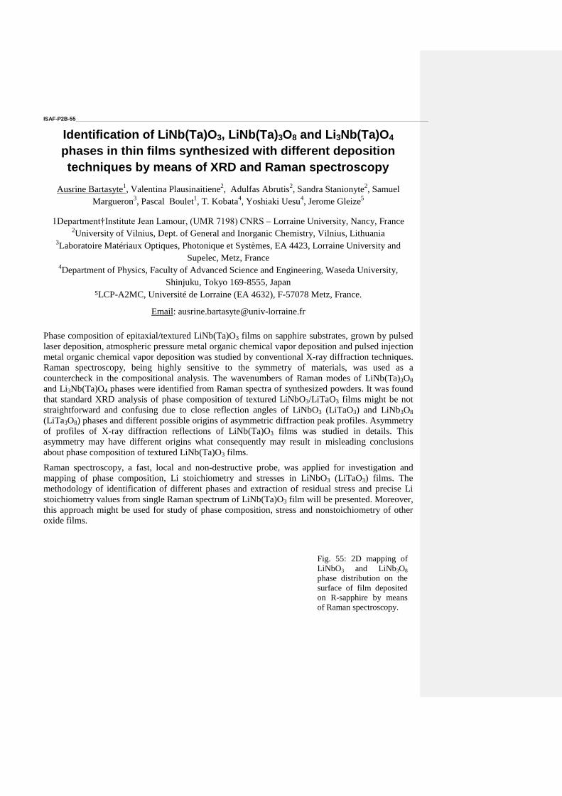
ISAF-P2B-55 ____________________________________________________________________________________________________________________
Identification of LiNb(Ta)O3, LiNb(Ta)3O8 and Li3Nb(Ta)O4
phases in thin films synthesized with different deposition
techniques by means of XRD and Raman spectroscopy
Ausrine Bartasyte1, Valentina Plausinaitiene
2, Adulfas Abrutis
2, Sandra Stanionyte
2, Samuel
Margueron3, Pascal Boulet
1, T. Kobata
4, Yoshiaki Uesu
4, Jerome Gleize
5
1Department†Institute Jean Lamour, (UMR 7198) CNRS – Lorraine University, Nancy, France 2University of Vilnius, Dept. of General and Inorganic Chemistry, Vilnius, Lithuania
3Laboratoire Matériaux Optiques, Photonique et Systèmes, EA 4423, Lorraine University and
Supelec, Metz, France 4Department of Physics, Faculty of Advanced Science and Engineering, Waseda University,
Shinjuku, Tokyo 169-8555, Japan 5LCP-A2MC, Université de Lorraine (EA 4632), F-57078 Metz, France.
Email: [email protected]
Phase composition of epitaxial/textured LiNb(Ta)O3 films on sapphire substrates, grown by pulsed
laser deposition, atmospheric pressure metal organic chemical vapor deposition and pulsed injection
metal organic chemical vapor deposition was studied by conventional X-ray diffraction techniques.
Raman spectroscopy, being highly sensitive to the symmetry of materials, was used as a
countercheck in the compositional analysis. The wavenumbers of Raman modes of LiNb(Ta)3O8
and Li3Nb(Ta)O4 phases were identified from Raman spectra of synthesized powders. It was found
that standard XRD analysis of phase composition of textured LiNbO3/LiTaO3 films might be not
straightforward and confusing due to close reflection angles of LiNbO3 (LiTaO3) and LiNb3O8
(LiTa3O8) phases and different possible origins of asymmetric diffraction peak profiles. Asymmetry
of profiles of X-ray diffraction reflections of LiNb(Ta)O3 films was studied in details. This
asymmetry may have different origins what consequently may result in misleading conclusions
about phase composition of textured LiNb(Ta)O3 films.
Raman spectroscopy, a fast, local and non-destructive probe, was applied for investigation and
mapping of phase composition, Li stoichiometry and stresses in LiNbO3 (LiTaO3) films. The
methodology of identification of different phases and extraction of residual stress and precise Li
stoichiometry values from single Raman spectrum of LiNb(Ta)O3 film will be presented. Moreover,
this approach might be used for study of phase composition, stress and nonstoichiometry of other
oxide films.
Fig. 55: 2D mapping of
LiNbO3 and LiNb3O8
phase distribution on the
surface of film deposited
on R-sapphire by means
of Raman spectroscopy.
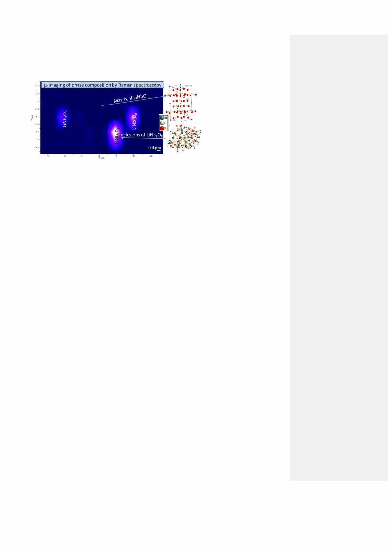
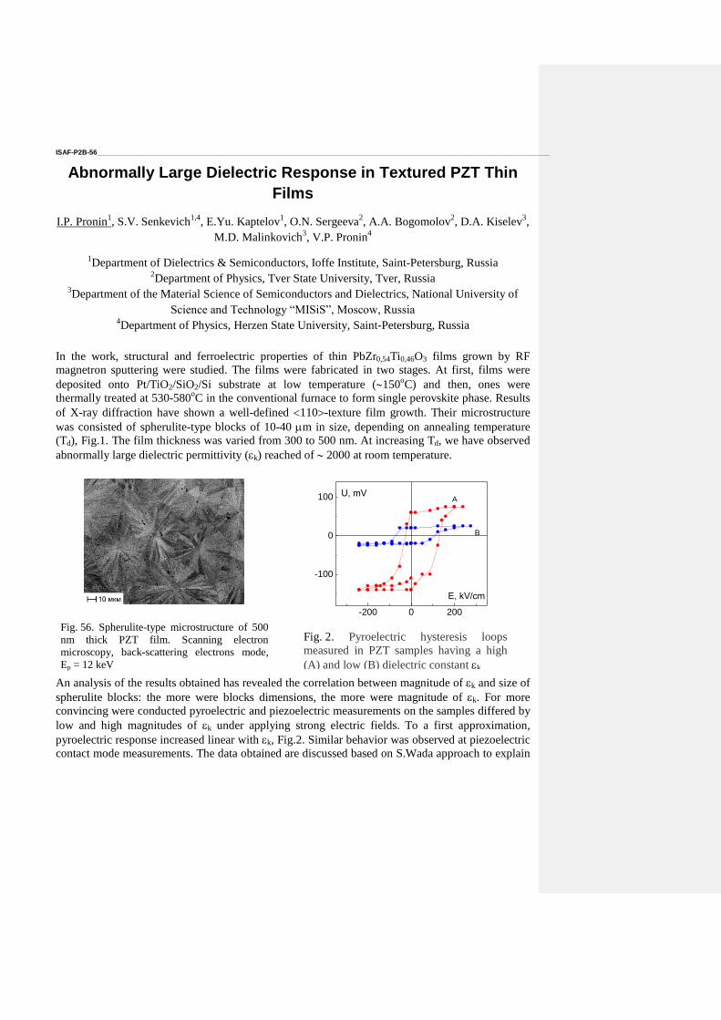
ISAF-P2B-56 ____________________________________________________________________________________________________________________
Abnormally Large Dielectric Response in Textured PZT Thin
Films
I.P. Pronin1, S.V. Senkevich
1,4, E.Yu. Kaptelov
1, O.N. Sergeeva
2, A.A. Bogomolov
2, D.A. Kiselev
3,
M.D. Malinkovich3, V.P. Pronin
4
1Department of Dielectrics & Semiconductors, Ioffe Institute, Saint-Petersburg, Russia
2Department of Physics, Tver State University, Tver, Russia
3Department of the Material Science of Semiconductors and Dielectrics, National University of
Science and Technology “MISiS”, Moscow, Russia 4Department of Physics, Herzen State University, Saint-Petersburg, Russia
In the work, structural and ferroelectric properties of thin PbZr0,54Ti0,46O3 films grown by RF
magnetron sputtering were studied. The films were fabricated in two stages. At first, films were
deposited onto Pt/TiO2/SiO2/Si substrate at low temperature (150oC) and then, ones were
thermally treated at 530-580oC in the conventional furnace to form single perovskite phase. Results
of X-ray diffraction have shown a well-defined 110-texture film growth. Their microstructure
was consisted of spherulite-type blocks of 10-40 m in size, depending on annealing temperature
(Td), Fig.1. The film thickness was varied from 300 to 500 nm. At increasing Td, we have observed
abnormally large dielectric permittivity (k) reached of 2000 at room temperature.
An analysis of the results obtained has revealed the correlation between magnitude of k and size of
spherulite blocks: the more were blocks dimensions, the more were magnitude of k. For more
convincing were conducted pyroelectric and piezoelectric measurements on the samples differed by
low and high magnitudes of k under applying strong electric fields. To a first approximation,
pyroelectric response increased linear with k, Fig.2. Similar behavior was observed at piezoelectric
contact mode measurements. The data obtained are discussed based on S.Wada approach to explain
-200 0 200
-100
0
100
Е, kV/cm
U, mVA
B
Fig. 2. Pyroelectric hysteresis loops
measured in PZT samples having a high
(A) and low (B) dielectric constant k
Fig. 56. Spherulite-type microstructure of 500
nm thick PZT film. Scanning electron
microscopy, back-scattering electrons mode,
Ep = 12 keV

giant piezoelectric response in ferroelectrics192
.
1 S. Wada, T. Muraishi, K.Yokoh, K. Yako, et.al. “Domain Wall Engineering in Lead-Free Ferroelectric Crystals”,
Ferroelectrics, vol. 355, p. 37-49, 2007
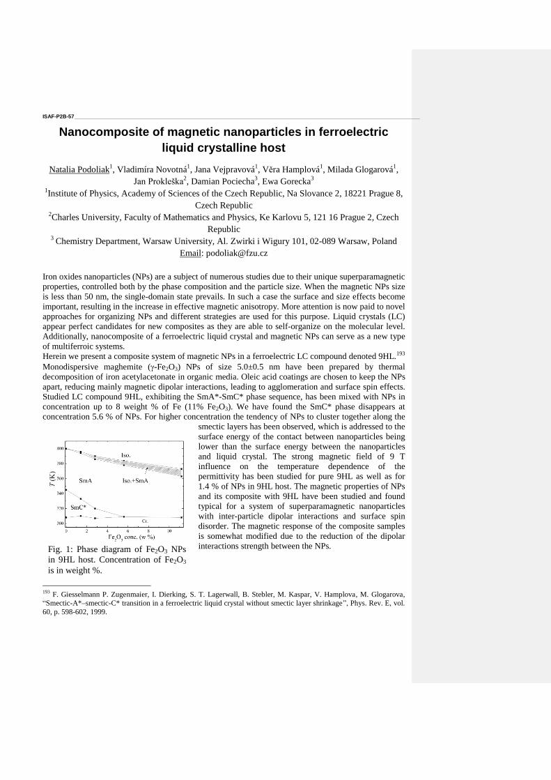
ISAF-P2B-57 ____________________________________________________________________________________________________________________
Nanocomposite of magnetic nanoparticles in ferroelectric
liquid crystalline host
Natalia Podoliak1, Vladimíra Novotná
1, Jana Vejpravová
1, Věra Hamplová
1, Milada Glogarová
1,
Jan Prokleška2, Damian Pociecha
3, Ewa Gorecka
3
1Institute of Physics, Academy of Sciences of the Czech Republic, Na Slovance 2, 18221 Prague 8,
Czech Republic 2Charles University, Faculty of Mathematics and Physics, Ke Karlovu 5, 121 16 Prague 2, Czech
Republic 3 Chemistry Department, Warsaw University, Al. Zwirki i Wigury 101, 02-089 Warsaw, Poland
Email: [email protected]
Iron oxides nanoparticles (NPs) are a subject of numerous studies due to their unique superparamagnetic
properties, controlled both by the phase composition and the particle size. When the magnetic NPs size
is less than 50 nm, the single-domain state prevails. In such a case the surface and size effects become
important, resulting in the increase in effective magnetic anisotropy. More attention is now paid to novel
approaches for organizing NPs and different strategies are used for this purpose. Liquid crystals (LC)
appear perfect candidates for new composites as they are able to self-organize on the molecular level.
Additionally, nanocomposite of a ferroelectric liquid crystal and magnetic NPs can serve as a new type
of multiferroic systems.
Herein we present a composite system of magnetic NPs in a ferroelectric LC compound denoted 9HL.193
Monodispersive maghemite (-Fe2O3) NPs of size 5.0±0.5 nm have been prepared by thermal
decomposition of iron acetylacetonate in organic media. Oleic acid coatings are chosen to keep the NPs
apart, reducing mainly magnetic dipolar interactions, leading to agglomeration and surface spin effects.
Studied LC compound 9HL, exhibiting the SmA*-SmC* phase sequence, has been mixed with NPs in
concentration up to 8 weight % of Fe (11% Fe2O3). We have found the SmC* phase disappears at
concentration 5.6 % of NPs. For higher concentration the tendency of NPs to cluster together along the
smectic layers has been observed, which is addressed to the
surface energy of the contact between nanoparticles being
lower than the surface energy between the nanoparticles
and liquid crystal. The strong magnetic field of 9 T
influence on the temperature dependence of the
permittivity has been studied for pure 9HL as well as for
1.4 % of NPs in 9HL host. The magnetic properties of NPs
and its composite with 9HL have been studied and found
typical for a system of superparamagnetic nanoparticles
with inter-particle dipolar interactions and surface spin
disorder. The magnetic response of the composite samples
is somewhat modified due to the reduction of the dipolar
interactions strength between the NPs.
193
F. Giesselmann P. Zugenmaier, I. Dierking, S. T. Lagerwall, B. Stebler, M. Kaspar, V. Hamplova, M. Glogarova,
“Smectic-A*–smectic-C* transition in a ferroelectric liquid crystal without smectic layer shrinkage”, Phys. Rev. E, vol.
60, p. 598-602, 1999.
Fig. 1: Phase diagram of Fe2O3 NPs
in 9HL host. Concentration of Fe2O3
is in weight %.

This work is supported by the Czech Science Foundation, projects No P204/11/0723 and No 13-14133S.
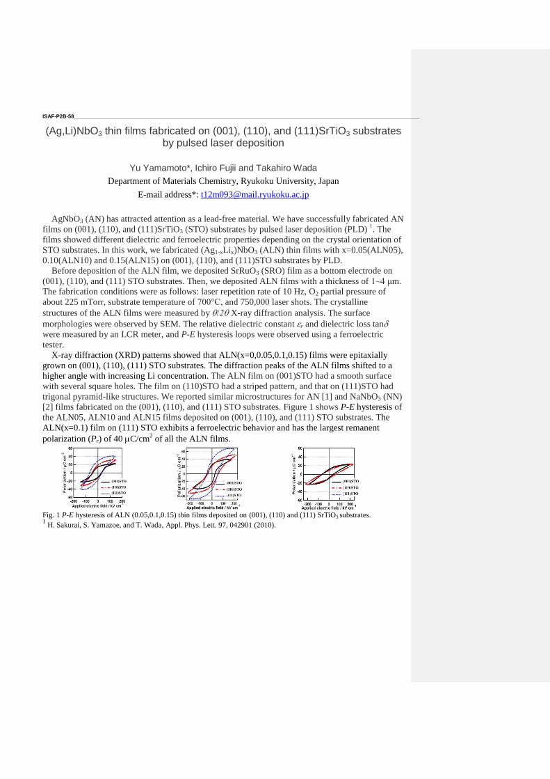
ISAF-P2B-58 ____________________________________________________________________________________________________________________
(Ag,Li)NbO3 thin films fabricated on (001), (110), and (111)SrTiO3 substrates by pulsed laser deposition
Yu Yamamoto*, Ichiro Fujii and Takahiro Wada
Department of Materials Chemistry, Ryukoku University, Japan
E-mail address*: [email protected]
AgNbO3 (AN) has attracted attention as a lead-free material. We have successfully fabricated AN
films on (001), (110), and (111)SrTiO3 (STO) substrates by pulsed laser deposition (PLD) 1. The
films showed different dielectric and ferroelectric properties depending on the crystal orientation of
STO substrates. In this work, we fabricated (Ag1-xLix)NbO3 (ALN) thin films with x=0.05(ALN05),
0.10(ALN10) and 0.15(ALN15) on (001), (110), and (111)STO substrates by PLD.
Before deposition of the ALN film, we deposited SrRuO3 (SRO) film as a bottom electrode on
(001), (110), and (111) STO substrates. Then, we deposited ALN films with a thickness of 1~4 μm.
The fabrication conditions were as follows: laser repetition rate of 10 Hz, O2 partial pressure of
about 225 mTorr, substrate temperature of 700°C, and 750,000 laser shots. The crystalline
structures of the ALN films were measured by /2 X-ray diffraction analysis. The surface
morphologies were observed by SEM. The relative dielectric constant r and dielectric loss tan
were measured by an LCR meter, and P-E hysteresis loops were observed using a ferroelectric
tester.
X-ray diffraction (XRD) patterns showed that ALN(x=0,0.05,0.1,0.15) films were epitaxially
grown on (001), (110), (111) STO substrates. The diffraction peaks of the ALN films shifted to a
higher angle with increasing Li concentration. The ALN film on (001)STO had a smooth surface
with several square holes. The film on (110)STO had a striped pattern, and that on (111)STO had
trigonal pyramid-like structures. We reported similar microstructures for AN [1] and NaNbO3 (NN)
[2] films fabricated on the (001), (110), and (111) STO substrates. Figure 1 shows P-E hysteresis of
the ALN05, ALN10 and ALN15 films deposited on (001), (110), and (111) STO substrates. The
ALN(x=0.1) film on (111) STO exhibits a ferroelectric behavior and has the largest remanent
polarization (Pr) of 40 C/cm2 of all the ALN films.
Fig. 1 P-E hysteresis of ALN (0.05,0.1,0.15) thin films deposited on (001), (110) and (111) SrTiO3 substrates. 1 H. Sakurai, S. Yamazoe, and T. Wada, Appl. Phys. Lett. 97, 042901 (2010).
ISAF-P2B-59 ____________________________________________________________________________________________________________________
Influences of MgTiO3 doping in Bi0.5Na0.5TiO3 on microstructure
and electrical parameters
Michael Naderer, Theresa Kainz, Klaus Reichmann
Christian Doppler Laboratory for Advanced Ferroic Oxides, Graz University of Technology, Graz,
Austria
Email: [email protected]
Bi0.5Na0.5TiO3 or BNT is one of the most promising candidates to replace Pb(Ti,Zr)O3 based
materials in ferroelectric applications. It was discovered in the 1960 by Smolenskii1 and receives
increasing attention since the commencement of the RoHS guideline2. Structurally, BNT forms a
complex rhombohedral perovskite with a 1 : 1 occupation of Bi3+
and Na+ on the 12-fold
coordinated A-site and Ti4+
on the 6-fold coordinated B-site.
The electrical and microstructural properties of BNT are highly modifiable. Doping of the system
can occur using hetero- or isovalent elements (e.g. Li+, Sr
2+, Nd
3+, Nb
5+) or by formation of solid
solutions with other perovskites (e.g. Bi0.5K0.5TiO3, BaTiO3, K0.5Na0.5NbO3). The second possibility
is the most common used, since it avoids high vacancy concentrations, which destabilizes the
structure and therefore leads to decomposition.
This work describes the impact of alloying BNT with MgTiO3 (MT) on the microstructure and
electrical parameters. Unlike the heavier earth alkaline metals, Magnesium does not form a
perovskite structure with Titanium. Despite the different structures of BNT and MT, solid solutions
can be formed and Mg2+
can be introduced into the BNT lattice, which acts as structural host.
The samples were prepared via a conventional mixed oxide route with Bi2O3, Na2CO3, MgO and
TiO2 as starting materials. The homogenization of the powder was carried out in a milling step
using Tungsten Carbide milling balls and bowl on a planetary mill. The calcination reaction was
performed at 800 °C to reduce the possibility of a Bi2O3-melt. The calcined powder was again ball
milled with the equipment mentioned before. Before sintering, PEG20000 was added as a binding
agent. The disc shaped samples, pressed with a diameter of 13 mm under a pressure of 150 MPa
were debindered at 450°C and subsequently sintered at 1100 °C for 5 h.
The theoretical density and cell parameters were obtained by X-Ray diffraction, the apparent
density was calculated using the Archimedes method. The microstructure was evaluated with SEM
imaging in channeling contrast mode, instead of etching, in order to visualize grain size and domain
structure. Secondary phase inclusions were also detected with SEM and EDX. 194
1. Smolenskii G, Isupov VA, Agranovskaya A, Krainik N. New ferroelectrics of complex composition. Sov. Phys. Solid
State. 1961;2(11):2651–2654.

ISAF-P2B-60 ____________________________________________________________________________________________________________________
Dopant effects on the phase diagram and piezoelectric properties of lead free piezoelectric niobate ceramics
Ruiping WANG1, Takuma ARIIZUMI
2, Junta ZUSHI
2, Seiji KOJIMA
2, and Hiroshi
BANDO1
1National Institute of Advanced Industrial Science and Technology, Tsukuba, Japan;
2University of Tsukuba, Tsukuba, Japan,
(Na0.5K0.5)NbO3 shows orthorombic sturcture at room temperature. Tetragonal is the
high temperature and rhombohedral is the low temperature phases of it. When ATiO3 (A =
Ba, Sr, Ca, Bi0.5Na0.5, Bi0.5K0.5, Bi0.5Li0.5, …) is mixed to it, the tetragonal phase could be tuned
to room temperature. And when BZrO3 (B = Ba, Sr, Ca, ...) is mixed to it, the rhombohedral
phase could be tuned to room temperature. Therefore, tetragonal-rhombohedral MPB could
be formed at room temperature by mixing (Na0.5K0.5)NbO3, ATiO3 and BZrO3 simultaneously.
It is reported that around the MPB, dielectric and piezoelectric properties were enhanced,
similar to that of PZT. To investigate effects of element additive on the dielectric and
piezoelectric properties of niobate ceramics, 0.92(Na0.5K0.5)NbO3-xBaZrO3-(0.08-
x)(Bi0.5K0.5)TiO3 (BBK) and 0.25 wt% MnO2 added BBK samples were prepared; and their
dielectric constant, electromechanical coupling coefficient kp, piezoelectric d33 constant,
mechanical quality factor Qm and so on were studied. Fig. 1 shows the composition dependence of kp, d33, and Qm,
respectively. kp is 15.16 % and d33 is 30 pC/N for x = 0.01. With
increasing x, both kp and d33 tend to increase. The highest kp and d33
values, 43.38 % and 279 pC/N were obtained in x = 0.05 for BBK, and
43.46 % in x = 0.05 and 369 pC/N in x = 0.06 for BBK+Mn,
respectively. That is for both BBK and BBK+Mn, piezoelectric
properties maximize around MPB. When x is beyond 0.05-0.06, kp as
well as d33 rapidly decrease. Composition dependence of dielectric
constant at room temperature maximize at around MPB, too.
Comparing piezoelectric properties of BBK and those of
BBK+Mn, it is clear that by adding Mn, kp, d33, and Qm are
all increased. That is BBK could be both hardened and
softened by adding Mn. The behaviors are attributed to the
oxygen vacancy formation and grain size growing,
respectively.
2. Amtsblatt der Europäischen Union. RICHTLINIE 2002/95/EG DES EUROPÄISCHEN PARLAMENTS UND DES
RATES vom 27. Januar 2003 zur Beschränkung der Verwendung bestimmter gefährlicher Stoffe in Elektro- und
Elektronikgeräten. 2003;L 37:19–23.
0.01 0.02 0.03 0.04 0.05 0.06 0.07
40
50
60
70
0
100
200
300
15
20
25
30
35
40
45
Qm
BaZrO3 content x
d3
3 (
pC
/N)
(c)
(b)
(a)
BBK
BBK+Mn
kp (
%)
MPB
Fig. 1 Composition dependence of
piezoelectric properties.
ISAF-P2B-61 ____________________________________________________________________________________________________________________
Influence of Germanium Substitution on Dielectric and
Ferroelectric Properties of Ba(Fe0.5Nb0.5)O3 Ceramics
Puripat Kantha1, Nuttapon Pisitpipathsin
1, Kamonpan Pengpat
1,*, Amar Bhalla
2
1Department of Physics and Materials Science, Faculty of Science, Chiang Mai University, Chiang
Mai 50200, Thailand 2Department of Electrical and Computer Engineering, College of Engineering,
University of Texas at San Antonio, Texas 78256, USA
Email: [email protected], [email protected],*
In this work, the influence of Ge4+
substitution on dielectric and ferroelectric properties of high
dielectric BaFe0.5Nb0.5O3 ceramics was studied. The BGFN powders with a formula
BaGex(Fe0.5Nb0.5)1-xO3 where x = 0.01, 0.015, 0.02 and 0.025 were produced via mixed-oxide
method and subsequently calcined at 1100-1200C for 4 h. To form the BGFN ceramics, the
resulting powders were pressed into pellets and sintered at various temperatures from 1200 to
1350C for 4 h in order to obtain the ceramic with maximum density under each condition. The
phase formation, microstructure and electrical properties of these ceramics were investigated. It was
found that the Ge4+
substitution played an important role on the change of crystal structures and the
phase formation of the BFN ceramics. The appearance of peak shift and peak split in XRD patterns
confirmed the structural change from cubic to monoclinic in the ceramic samples at higher Ge4+
content. The ceramics with x 0.015 contained three phases of BGFN, Ba3Fe2Ge4O14 and BaGeO3.
The amount of each phase was depended on the concentration of Ge4+
where the Ba3Fe2Ge4O14 and
BaGeO3 phases were found to increase with increasing x content. It was also found that the slightly
lower densification, higher porosity and smaller grain sizes were found in the BGFN ceramics with
higher level of Ge4+
addition. This in turn affected their dielectric properties where dielectric
constant was substantially decreased while the dielectric loss was greatly improved. The optimum
composition for this system was found to be x = 0.015, where the maximum dielectric constant
(~12282) with lower dielectric loss at room temperature were obtained.
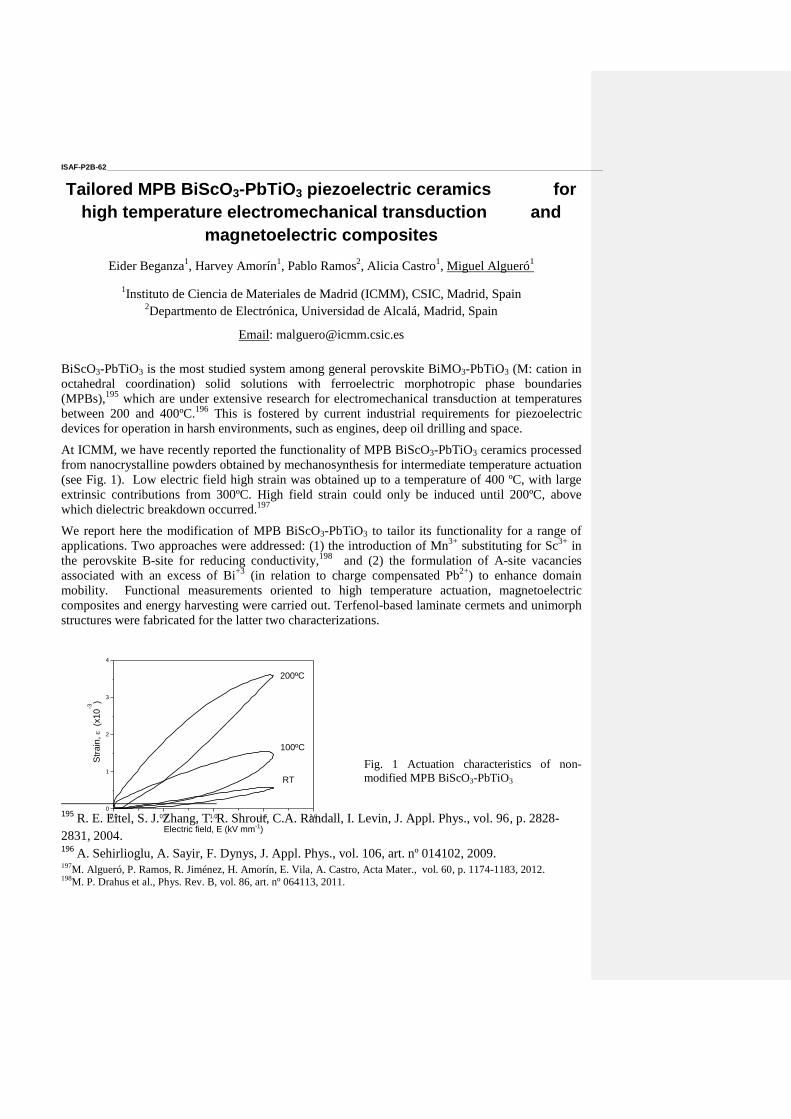
ISAF-P2B-62 ____________________________________________________________________________________________________________________
Tailored MPB BiScO3-PbTiO3 piezoelectric ceramics for
high temperature electromechanical transduction and
magnetoelectric composites
Eider Beganza1, Harvey Amorín
1, Pablo Ramos
2, Alicia Castro
1, Miguel Algueró
1
1Instituto de Ciencia de Materiales de Madrid (ICMM), CSIC, Madrid, Spain
2Departmento de Electrónica, Universidad de Alcalá, Madrid, Spain
Email: [email protected]
BiScO3-PbTiO3 is the most studied system among general perovskite BiMO3-PbTiO3 (M: cation in
octahedral coordination) solid solutions with ferroelectric morphotropic phase boundaries
(MPBs),195
which are under extensive research for electromechanical transduction at temperatures
between 200 and 400ºC.196
This is fostered by current industrial requirements for piezoelectric
devices for operation in harsh environments, such as engines, deep oil drilling and space.
At ICMM, we have recently reported the functionality of MPB BiScO3-PbTiO3 ceramics processed
from nanocrystalline powders obtained by mechanosynthesis for intermediate temperature actuation
(see Fig. 1). Low electric field high strain was obtained up to a temperature of 400 ºC, with large
extrinsic contributions from 300ºC. High field strain could only be induced until 200ºC, above
which dielectric breakdown occurred.197
We report here the modification of MPB BiScO3-PbTiO3 to tailor its functionality for a range of
applications. Two approaches were addressed: (1) the introduction of Mn3+
substituting for Sc3+
in
the perovskite B-site for reducing conductivity,198
and (2) the formulation of A-site vacancies
associated with an excess of Bi+3
(in relation to charge compensated Pb2+
) to enhance domain
mobility. Functional measurements oriented to high temperature actuation, magnetoelectric
composites and energy harvesting were carried out. Terfenol-based laminate cermets and unimorph
structures were fabricated for the latter two characterizations.
Fig. 1 Actuation characteristics of non-
modified MPB BiScO3-PbTiO3
195 R. E. Eitel, S. J. Zhang, T. R. Shrout, C.A. Randall, I. Levin, J. Appl. Phys., vol. 96, p. 2828-
2831, 2004. 196 A. Sehirlioglu, A. Sayir, F. Dynys, J. Appl. Phys., vol. 106, art. nº 014102, 2009. 197
M. Algueró, P. Ramos, R. Jiménez, H. Amorín, E. Vila, A. Castro, Acta Mater., vol. 60, p. 1174-1183, 2012. 198
M. P. Drahus et al., Phys. Rev. B, vol. 86, art. nº 064113, 2011.
0.0 0.5 1.0 1.5 2.0
0
1
2
3
4
200ºC
Str
ain
,
(x10
-3
)
Electric field, E (kV mm-1)
RT
100ºC
ISAF-P2B-63 ____________________________________________________________________________________________________________________
Lead-free fibers with oriented structure
Bortolani Francesca1, Lusiola Tony
1, Clemens Frank
1
1Laboratory for High Performance Ceramics, Empa, Dübendorf, Switzerland
Email: [email protected]
In the past ten years, the use of lead in piezoelectric ceramics has been drastically reduced and the
attention has moved to lead-free materials. KNN-based ceramics are good candidates as alternatives
to PTZ, but their properties have to be improved in order to reach the PZT ones. A way to achieve
this target is by grain orientation.
Platelet-like templates, with dimensions of ~20x10x3µm, have been obtained by molten salt
synthesis (MSS) and incorporated with anisotropic powder. By thermoplastic extrusion, the
platelets have been oriented and KNN ceramic fibers were developed. The templates act as seeds
during sintering and fibers with an oriented structure are eventually obtained. Microstructural
characterisation of the ceramic fibers is shown. Ferroelectric behaviour of single fibers is also
analysed by the use of a unique equipment in terms of hysteresis loop, butterfly loop (S-E) and
piezoelectric coefficient (d33).
ISAF-P2B-64 ____________________________________________________________________________________________________________________
Effect of Sn4+
substitution on structure and properties in the
PbSnO3–PbZrO3–PbTiO3 ternary system
Zhuo Xing, Xiaoyong Wei, Li Jin
Electronic Materials Research Laboratory, Key Laboratory of the Ministry of Education & In-
ternational Center for Dielectric Research, Xi’an Jiaotong University, Xi’an 710049, China
Email: [email protected]
Piezoelectric materials have been extensively investigated in the last few decades for device
applications, because of their multifunctional properties, which can be used in a broad range of
applications. Piezoelectric properties are dependent on multiple variables, such as mophotropy,
defect structure, grain size, domain size and density. Piezoelectric ceramics in the PbSnO3–PbZrO3–
PbTiO3 (PZST) ternary system with pure perovskite structure were synthesized by conventional
solid state reaction method. Morphotropic phase boundary (MPB) compositions were confirmed by
X-ray diffraction. The influence of Sn4+
on dielectric, piezoelectric, and ferroelectric properties of
PZTST was investigated systematically. The experimental results showed that the perovskite
structure changed from tetragonal to rhombohedral symmetry and the Curie temperature (TC)
decreased gradually with increasing the content of PbSnO3. The composition with Zr:Sn=1:1
ceramics exhibited favorable properties of d33, d31, Qm, kp, TC, Ec.
ISAF-P2B-65 ____________________________________________________________________________________________________________________
Novel series of temperature stable glass free LTCC Li2BO4-TiO2
(B=Mo, W)
Jing Guo1, Di Zhou
1, Gaoqun Zhang
1, Hong Wang
1
1Electronic Materials Research Laboratory, Key Laboratory of the Ministry of Education &
International Center for Dielectric Research, Xi’an Jiaotong University, Xi’an 710049, China
Email: [email protected]
In this work, a new series of (1-x)Li2BO4-xTiO2 (B=Mo, W) ceramics were developed for
microwave dielectric applications. They were prepared by solid state reaction method and the phase
composition, microstructures, sintering behaviors, chemical compatibility with silver and
microwave dielectric properties were investigated. Li2BO4 (B=Mo, W) ceramics with ultra-low
sintering temperatures (<650 oC) exhibit good microwave dielectric properties (permittivity εr= 5.5,
Q×f= 46,000~62,000 GHz), but all of them have large negative temperature coefficient of resonant
frequency (τf = -146 to -160 ppm/oC). In order to compensate the negative τf values of Li2BO4
ceramics, rutile TiO2 was selected to form (1-x)Li2BO4-xTiO2 (B=Mo, W) mixtures. The X-ray
diffraction pattern and scanning electron microscope analysis revealed that the Li2BO4 did not react
with rutile TiO2 and a stable two-phase composite system Li2BO4-TiO2 was formed. At x = 0.45 ~
0.50, temperature stable microwave dielectric materials were obtained: εr = 10.1~12.2, Qf =
29,300~34,800 GHz, and TCF ~ 0 ppm/oC.
ISAF-P2B-66 ____________________________________________________________________________________________________________________
Investigating the effects of Ba-, Ca- and Sr-doping on the
properties of PLZT
Mirjam Skof, Theresa Kainz, Klaus Reichmann
Christian Doppler Laboratory for Advanced Ferroic Oxides, Graz University of Technology, Graz,
Austria
E-Mail: [email protected]
Leadzirconate is an antiferroelectric material with interesting properties for storing charge at
elevated electric fields. By replacing some of the Zr with Ti the antiferroelectric phase is
destabilized in favor of a ferroelectric phase. Introducing La3+
as a substituent for Pb2+
generates A-
site vacancies, thus stabilizing the antiferroelectric phase at higher Ti contents. Isovalent doping
causes no changes in the vacancy concentration but leads to effects due to differences in mass and
ionic radii.
Antiferroelectric to ferroelectric phase changes can be induced by applying a critical electric field
causing a structural phase change resulting from the parallel alignment of anti-parallel dipoles. This
enables a large increase in stored energy. Withdrawing the electrical field leads to a hysteretic
recovery of the antiferroelectric phase.
In this study the influence of earth alkaline dopants on the properties of PLZT was investigated.
Two basic compositions with differing Zr-/Ti-content were doped with Ba, Ca and Sr according to
the formula (Pb0,89AE0,02La0,06)(Zr1-xTix)O3 (AE = Ca, Sr, Ba; x = 0,10 & 0,15). The ceramic
powders were processed via the mixed oxide route, calcined at 925°C and sintered at 1250°C. An
excess of 2 % lead was added prior calcination.
After the preparation the samples were examined with XRD to control the formation of the
perovskite structure and to observe changes in the volume of the unit cell. The sintering behavior of
the ceramic was investigated with dilatometry.
To display the microstructure scanning electron microscopy was used in the channeling contrast
mode instead of etching. The chemical composition of the samples was analyzed via EDX.
The dielectric properties were measured by determining the relative permittivity, the loss factor as
well as their temperature dependence. Furthermore polarization curves were recorded leading to the
switching field. The results were compared according to the chemical composition of the samples.
ISAF-P2B-67 ____________________________________________________________________________________________________________________
Characterization and synthesis of Barium Titanate/Ni-nano metal
composite by sol-gel process for high voltage capacitor
I S Kim1 , Mohsin Saleem
2, J S Song
3, S J Jeong
4 and M S Kim
5
1,3,4,5
Battery Research Center, KERI, Changwon, Republic of Korea, 641-120 2 Department of Electrical Functionality Material engineering,
University of Science and Technology, Daejeon, Republic of Korea 305-333
Email: [email protected]
A modified method has been applied to synthesize high purity Barium nickel titanate powder in
nanometer range by sol-gel process. Conventionally, Barium titanate is synthesized by solid-state
reaction between BaCO3 and TiO2. The electrical behavior of barium titanate ceramics strongly
depend on the composition and the microstructure. Because it is chemically and mechanically very
stable, exhibits ferroelectric properties at and above room temperature, because it can be easily
prepared and used in the form of ceramic polycrystalline samples. Due to its high dielectric constant
and low dielectric loss characteristics barium titanate (BaTiO3) has been used in applications such
as high voltage capacitors and energy storage devices.
In this paper, BaTiO3-Ni composite is prepared by sol-gel technique with nickel content of different
concentration for charge island in high voltage capacitors. It is thermally heated in anti-oxidation
furnace. The electrical properties were characterized in term of relative permittivity, conductivity,
C-V measurements. The electrical properties were affected by the conducting phase with increase in
dielectric constant. The dielectric constant is increased from 5000 to 6000 by 10 to 15 % nickel
paste which is high as compared to BaTiO3-Ni synthesize by solid state process. Phase
transformation and crystallite size of the powder were investigated by X-ray diffraction method;
particle morphology and size were studied by scanning electron microscope. We suggested that a
dielectric material is highly suitable for high voltage capacitors.
ISAF-P2B-68 ____________________________________________________________________________________________________________________
Sintering and Dielectric Properties of (1-x) BaTiO3 –x Sr3Ti2O7 Composite
Ceramics by a Coating Method Chaojun Xie, Dengren Jin, Lixin Zhou, Hanting Dong, Jinrong Cheng
School of Materials Science and Engineering, Shanghai University, Shanghai, China
Email: [email protected]
Sintering and dielectric properties of (1-x) BaTiO3–xSr3Ti2O7 composite ceramics fabricated by a
coating method were investigated. In this research, the Ruddlesden-Popper(RP) Phase Sr3Ti2O7
powders and BaTiO3 powders were synthetized by the solid reaction, respectively, and then their
mixed powders were coated with BaTiO3 sol-gel by using ultrasonic irradiation. The structure
evolution of the BaTiO3 coating layer was investigated via transmission electron microscopy.
Microstructure and phase variation, and ions inter-diffusion during the sintering were investigated
by scanning electron microscopy and X-ray diffraction, respectively. Results show that the
permittivity and dielectric loss were sharply decreased and temperature stability was improved
effectively, due to the existence of ordered SrO-OSr stacking faults and the formation of an
inhomogeneous micro-region nearby the grain boundary through the tuning of sintering schedules
and the BaTiO3 content.
ISAF-P2B-69 ____________________________________________________________________________________________________________________
Processing and properties of BiFeO3-PbTiO3-Pb(Mn1/3Nb2/3)O3 ternary system
for high Curie temperature piezoceramics
Rui Dai, Shundong Bu, Dalei Wang, Dengren Jin and Jinrong Cheng*199
1 School of materials science and engineering, shanghai University, Shanghai 200072
BiFeO3-PbTiO3-Pb(Mn1/3Nb2/3)O3 ternary solid solution system was investigated for the
development of piezoelectric ceramics with high Curie temperature. (1-x)(0.7BiFeO3-0.3PbTiO3)-
xPb(Mn1/3Nb2/3)O3 (BFPT-PMN) for x=0.03, 0.04, 0.05, 0.06 and 0.1 ternary ceramics were
fabricated by the conventional mixed oxide ceramic. XRD patterns reveal that all compositions possess perovskite
structure with a rhombohedral symmetry and columbite disappears with the extension of dwell time.
The surface morphology was examined by SEM. The dielectric property measurement on the
ceramics confirmed the high Curie temperature and the improved loss tangent with the
Pb(Mn1/3Nb2/3)O3 doping. The values of dielectric constant, loss tangent and the Curie temperature
were 314, 0.01 and 630 oC for x=0.03 at the sintering of 1040
oC and at the frequency of 10
3 Hz.
Keywords: BFPT-PMN ternary system; High Curie temperature; Dielectric properties;
Corresponding author: email:

Integration and Tailored Micro/Nanostructures
CLUB A
Wednesday, July 24 2013, 10:30 am - 12:00 pm
Chair: Tadej Rojac
Jozef Stefan Institute
ISAF2-G1-1 _____________________________________________________________________________________________________________________
Chemical Solution Processing of Ferroelectric Thin Films and
Nanostructures
Nazanin Bassiri-Gharb1, 2
, Ashley Bernal1, Yaser Bastani
1, Suenne Kim
3, Elisa Riedo
3, Haidong
Lu4, Alexei Gruverman
4, Amit Kumar
5, Sergei Kalinin
5
1 G.W. Woodruff School of Mechanical Engineering, Georgia Institute of Technology, Atlanta, GA,
USA 2
School of Materials Science and Engineering, Georgia Institute of Technology, Atlanta, GA, USA 3 School of Physics, Georgia Institute of Technology, Atlanta, GA, USA
4 Department of Physics and Astronomy, University of Nebraska-Lincoln, Lincoln, NE, USA
5 Center for Nanophase Materials Science, Oak Ridge National Laboratory, Oak Ridge, TN, USA
Email: [email protected]
Ferroelectric (FE) thin films and nanostructures find a wide range of applications in capacitive
elements, non-volatile memories, micro/nano-electromechanical system (MEMS/NEMS) sensors,
actuators and transducers, as well as energy harvesting nano- and micro-generators. With the drive
towards miniaturization, multiple intrinsic and extrinsic factors need to be leveraged in order to
increase and/or maintain the high dielectric and piezoelectric response of ferroelectric materials and
reduce size effects. However, the currently available processing methods, mostly based on pre-
existing micromachining fabrication methods, suffer multiple limitations. Top-down approaches
can damage surface layers due to the impact of high-energy particles (detrimental to the final
electromechanical properties), or offer poor side-wall definition in wet-etch methods. Bottom-up
approaches, while allowing creation of high quality ferroelectric materials, are mostly limited in
patterning capability and compatibility for alignment with previous and subsequent layers.
Chemical solution deposition provides a very flexible approach for processing of short and high-
aspect ratio ferroelectric nanostructures, as well as thin and ultrathin ferroelectric films with
controlled crystallographic orientation and enhanced dielectric and piezoelectric response on a
variety of substrates.
This talk gives an overview of the processing methods developed in our group for such structures
and thin films. Specifically, we report the results of a lift-mode AFM, employing a heated tip, used
to locally crystallize sol-gel films of ferroelectric materials (e.g. PbTiO3 and PbZr1-xTixO3).
Arbitrary shapes and periodic arrays of ferroelectric nanostructures are obtained on platinized soda-
lime glass, silicon and polyimide substrates. The feature size ranged between ~10 nm and 2.5 μm.
An alternative method for creation of ferroelectric microstructure is also explored by leveraging
thermally decomposable, UV or e-beam patterned, sacrificial material. The photoresist or e-resist
patterns are created via deep-UV lithography or e-beam patterning. A subsequent coating with the
appropriate chemical solution precursor of the ferroelectric material, followed by heat treatment
leads to crystallization of the ferroelectric and removal of the sacrificial patterns. Modification of
the heat treatment profile and relative thicknesses of the resist/ferroelectic precursor result into
creation of surface micro/nano-channels of ferroelectric material or alternatively patterned
ferroelectric areas.
ISAF2-G1-2 _____________________________________________________________________________________________________________________
Confinement Printing of Thin Film Lead Zirconate Titanate for MEMS Applications
A. J. Welsh1, D. Dezest
2, L. Nicu
2, M. A. Hickner
1, and S. Trolier-McKinstry
1
1The Pennsylvania State University, N-224 Millennium Science Complex, University Park, USA
2Laboratoire d’Analyse et d’Architecture des Systemes – Le Centre National de la Recherche
Scientifique, University de Toulouse, Toulouse, France
Email: [email protected]
Thin film electroceramics used as sensors, capacitors, actuators, etc. are patterned into
specific geometries, typically by either a wet or dry subtractive patterning approach. It is also
interesting to consider additive patterning techniques for MEMS applications. Ceramic suspensions,
pastes, and solutions have been additively patterned at the macro and meso-scale through the use of
inkjet printing, screen printing, and embossing. Powder-free ceramic solutions have been patterned
through soft lithographic techniques. Soft lithography utilizes elastomeric polymer stamps/molds to
confine or deposit solutions onto a substrate. Printing of a ceramic solution from stamp protrusions
directly onto a substrate, termed microcontact printing, has been used to deposit patterned lead
zirconate titanate (PZT) thin films with comparable electrical properties to continuous PZT thin
films. However, this technique deposits very thin layers of ceramic for every stamping cycle which
is a concern for pattern registry. Elastomeric polymers have also been used as molds for ceramic
solutions in order to deposit the film in a single processing step. These patterning techniques
produce features that have large shape deformations or cracking of the final films.
This work explores the confinement printing of PZT liquid precursors from stamp wells
(rather than stamp protrusions as is used in microcontact printing). The confinement printing of
solutions uses an initial sacrificial printing step in order to remove solution from the protrusions of
the stamp. The second stamping cycle deposits the solution from the wells of stamp. Printing from
wells doubled the thickness (e.g. from 25 to 50 nm) of deposited solution per stamping cycle over
microcontact printing. This work studies the printing characteristics of this patterning technique,
including line edge resolution, feature thickness, side wall angels, and achievable lateral feature
size. Arrays of PZT features were printed, characterized and compared to continuous PZT thin films
of similar thickness. One micron thick printed PZT features exhibit a permittivity of 1030 and a loss
tangent of 0.024. The hysteresis loops are well formed, without pinching of the loops. The patterned
features showed remanent polarizations of 29µC/cm2, and coercive fields of 52kV/cm. The
piezoelectric response of the features produced an e31,f of -7 C/m2.
Fig. 1. Electron holography images of an individual 10 nm
BaTiO3 nanocube below (a) and above (b)the Curie
temperature demonstrating the polarization structure in the
ferroelectric state and its eradication above the phase transition
temperature
ISAF2-G1-3 _____________________________________________________________________________________________________________________
Ferroelectric Order in Nanoscale Perovskites and its Control via Colloidal
Processing
Gabriel Caruntu1,2
, Amin Yourdkhani1,2
, Mark J. Polking3,4
, Daniela Caruntu1, Valeri Petkov
5,
Christian F. Kisielowski6, Vyacheslav V. Volkov
7, Yimei Zhu
6, A. Paul Alivisatos
8 and
Ramamoorthy Ramesh9
1Advanced Materials Research Institute, University of New Orleans, New Orleans, Louisiana
70148, USA 2Department of Chemistry, University of New Orleans, New Orleans, LA 70148, USA
3Department of Materials Science and Engineering, University of California, Berkeley, Berkeley, CA 94720, USA
4Department of Chemistry, Harvard University, Boston, Massachusetts, USA
5Department of Physics, Central Michigan University, Mount Pleasant, MI 48859, USA
6National Center for Electron Microscopy, Lawrence Berkeley National Laboratory, Berkeley, CA 94720, USA
7Condensed Matter Physics and Materials Sciences Department, Brookhaven National Laboratory, Upton, NY 11973,
USA 8Department of Chemistry, University of California, Berkeley, Berkeley, CA 94720, USA.
9Materials Sciences Division, Lawrence Berkeley National Laboratory, Berkeley, CA 94720, USA
In an attempt to address one of the fundamental questions related to the survival of
feroelectricity in technologically important perovskites, we present here an atomic-scale insight into
the fundamental nature of ferroelectric order down to its ultimate size limit using. To this end we
used monodisperse, aggregate-free BaTiO3 colloidal nanocrystals as a model system.
Atomic resolution mapping of local ferroelectric distortions indicates a coherent, nearly linear,
monodomain state accompanied by local structural distortions. The persistence of ferroelectric
coherence in BaTiO3 is further supported by single-particle studies with off-axis electron
holography and PFM measurements of individual nanocubes demonstrating ferroelectric switching
behaviour at room temperature. These PFM
studies further demonstrate the ultimate
stability limit of ferroelectric order. Careful
atomic PDF studies point to the parallel
roles played by surface-induced relaxation
and depolarization effects in the dissolution
of ferroelectric order at finite dimensions
and indicate considerable structural
disorder and dipole decoherence, even in
conductive GeTe with strong polarization
screening. These studies also demonstrate
the utility of colloidal morphology control
as a means of stabilizing the polar state at nanoscale dimensions. These experiments reveal the
ultimate limit of the ferroelectric state and provide a pathway to unravelling the fundamental
physics of nanoscale ferroelectricity at the smallest possible size scales.
ISAF2-G1-4 _____________________________________________________________________________________________________________________
Structural and Electric Properties of Ca2Nb3O10 Thin Films
grown by Electrophoretic Method
Sang Hyo Kweon1, Mir Im
1, Sahn Nahm
1
1Department of Material Science and Engineering, Korea University, Seoul, South Korea
Email: [email protected]
KCa2Nb3O10 ceramics, Dion-Jacobson layered perovskite materials, have been widely investigated
because they can be easily exfoliated to the nano-sized sheets which can be used to the future
multilayer capacitors with a small size and high performance. A KCa2Nb3O10 phase was formed at
900oC and a dense ceramics were obtained after sintering at 1375
oC for 10 h. A proton exchange
process was carried out to produce the intermediate phase of HCa2Nb3O10 and the stable
(Ca2Nb3O10)- nanosheet colloids were formed using the mixture of the HCa2Nb3O10 powders,
tetrabutylammonium hydroxide (TBAOH) solution and water having the same TBA+/H
+ ratio. The
exfoliated (Ca2Nb3O10)- nanosheets were dispersed into the acetone intermediate, which was used to
form the thin film by the electrophoretic method under 100 V electric source. The electrophoretic
thin films were then annealed at various temperatures for 30 min under air condition and all the
films have the Ca2Nb3O10 phase. In particular, a high dielectric constant of 65 with a loss of 2.1% at
100 kHz was obtained from the film annealed at 600oC and this film also showed the low the
leakage current density of 1*10-7
A/cm2 at 0.1 MV/cm.
ISAF2-G1-5 _____________________________________________________________________________________________________________________
Multiferroic Properties of Bismuth Ferrite Porous Thin Films
Stella Skiadopoulou, Eliana Carvalho, Alichandra Castro, Paula Ferreira, Paula M. Vilarinho
Department of Materials and Ceramic Engineering, CICECO, University of Aveiro, Aveiro,
Portugal
Email: [email protected]
Magnetoelectric multiferroics’ ability of magnetic field manipulation via electric fields or vice versa
can be extremely promising for information storage applications, leading to thinner, as well as
flexible devices, with significantly high energetic efficiencies and huge capacities200
. Bismuth
ferrite (BiFeO3), being the only single-phase multiferroic at room temperature, is considered the
model multiferroic201
. Porous matrices, apart from providing lighter devices, have a great
importance for a large range of applications, since novel architectures can be achieved by the
incorporation of diverse materials in the pores, producing multifunctional films202
.
For that purpose, BiFeO3 porous thin films were prepared by combination of simple processes:
modified sol-gel (with a block copolymer), Evaporation Induced Self-Assembly (EISA) method and
dip-coating deposition on Pt/TiO2/SiO2/Si substrates. Different copolymer concentrations were used
in the as-prepared solutions, in order to study the effect of porosity on the multiferroic properties.
Additionally, film deposition was conducted at increasing deposition velocities, aiming at the
characterization of films with varying thicknesses. Ferroelectric and ferromagnetic properties were
studied at the nanoscale via Piezoresponse Force Microscopy (PFM) and Magnetic Force
Microscopy (MFM) respectively. Dense films with similar characteristics were prepared for
comparison proposes.
The variations in the piezoresponse signal of porous films with increasing porosity and decreasing
thickness is discussed and related with the microstructure of the films, domain configuration and
substrate interaction.
Acknowledgment
The authors are grateful to FCT and FEDER (QREN - COMPETE) for financial support
PTDC/CTM/098130/2008).
200
Spaldin, N.A., S.W. Cheong, and R. Ramesh, Multiferroics: Past, present, and future. Physics Today, vol. 63, p. 38-
43, 2010. 201
Martin, L.W. and R. Ramesh, Overview No. 151 Multiferroic and magnetoelectric heterostructures. Acta Materialia,
vol. 60, p. 2449-2470, 2012. 202
Ferreira, P., et al., Nanoporous Piezo- and Ferroelectric Thin Films. Langmuir, vol. 28, p. 2944-2949, 2012.

Pb-Free Piezoelectrics
CLUB B
Wednesday, July 24 2013, 10:30 am - 12:00 pm
Chair: Clive Randall
Pennsylvania State University
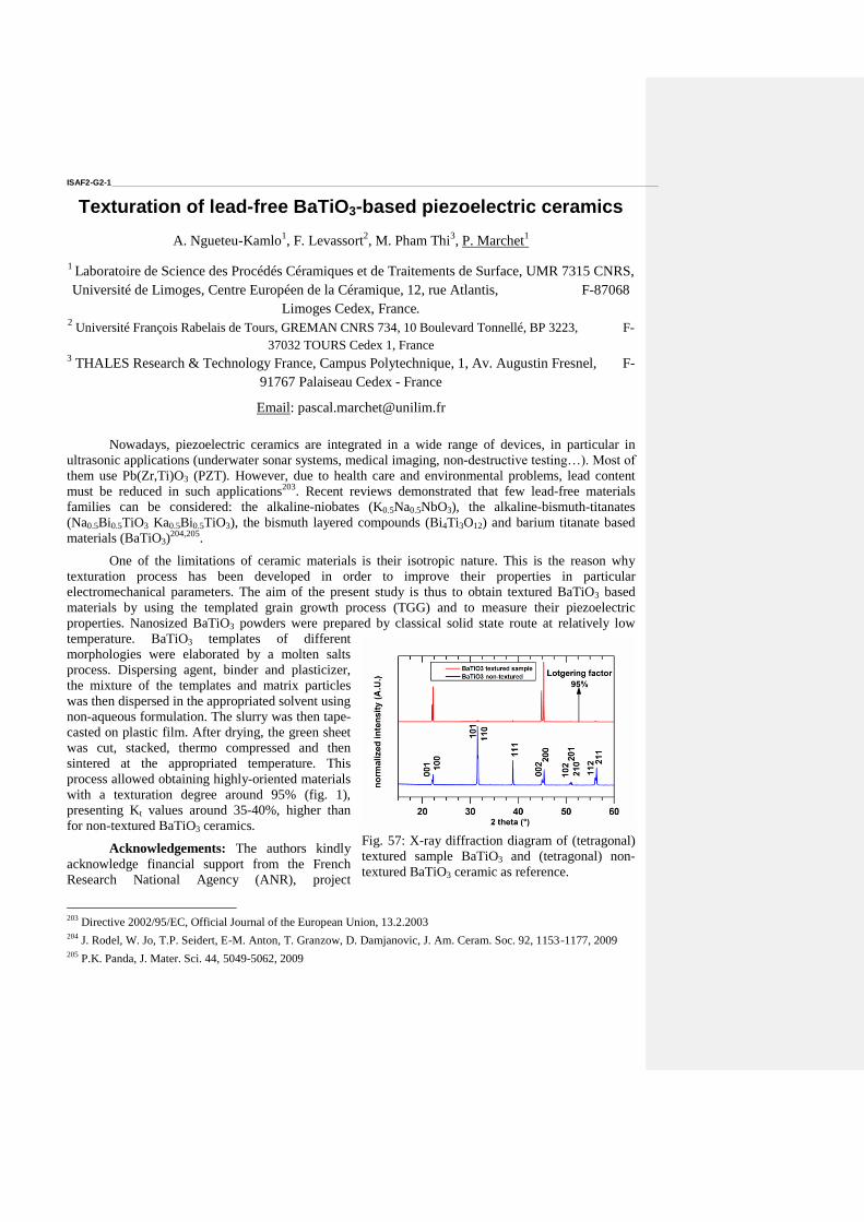
ISAF2-G2-1 _____________________________________________________________________________________________________________________
Texturation of lead-free BaTiO3-based piezoelectric ceramics
A. Ngueteu-Kamlo1, F. Levassort
2, M. Pham Thi
3, P. Marchet
1
1 Laboratoire de Science des Procédés Céramiques et de Traitements de Surface, UMR 7315 CNRS,
Université de Limoges, Centre Européen de la Céramique, 12, rue Atlantis, F-87068
Limoges Cedex, France. 2 Université François Rabelais de Tours, GREMAN CNRS 734, 10 Boulevard Tonnellé, BP 3223, F-
37032 TOURS Cedex 1, France 3 THALES Research & Technology France, Campus Polytechnique, 1, Av. Augustin Fresnel, F-
91767 Palaiseau Cedex - France
Email: [email protected]
Nowadays, piezoelectric ceramics are integrated in a wide range of devices, in particular in
ultrasonic applications (underwater sonar systems, medical imaging, non-destructive testing…). Most of
them use Pb(Zr,Ti)O3 (PZT). However, due to health care and environmental problems, lead content
must be reduced in such applications203. Recent reviews demonstrated that few lead-free materials
families can be considered: the alkaline-niobates (K0.5Na0.5NbO3), the alkaline-bismuth-titanates
(Na0.5Bi0.5TiO3 Ka0.5Bi0.5TiO3), the bismuth layered compounds (Bi4Ti3O12) and barium titanate based
materials (BaTiO3)204,205.
One of the limitations of ceramic materials is their isotropic nature. This is the reason why
texturation process has been developed in order to improve their properties in particular
electromechanical parameters. The aim of the present study is thus to obtain textured BaTiO3 based
materials by using the templated grain growth process (TGG) and to measure their piezoelectric
properties. Nanosized BaTiO3 powders were prepared by classical solid state route at relatively low
temperature. BaTiO3 templates of different
morphologies were elaborated by a molten salts
process. Dispersing agent, binder and plasticizer,
the mixture of the templates and matrix particles
was then dispersed in the appropriated solvent using
non-aqueous formulation. The slurry was then tape-
casted on plastic film. After drying, the green sheet
was cut, stacked, thermo compressed and then
sintered at the appropriated temperature. This
process allowed obtaining highly-oriented materials
with a texturation degree around 95% (fig. 1),
presenting Kt values around 35-40%, higher than
for non-textured BaTiO3 ceramics.
Acknowledgements: The authors kindly
acknowledge financial support from the French
Research National Agency (ANR), project
203
Directive 2002/95/EC, Official Journal of the European Union, 13.2.2003 204
J. Rodel, W. Jo, T.P. Seidert, E-M. Anton, T. Granzow, D. Damjanovic, J. Am. Ceram. Soc. 92, 1153-1177, 2009 205
P.K. Panda, J. Mater. Sci. 44, 5049-5062, 2009
Fig. 57: X-ray diffraction diagram of (tetragonal)
textured sample BaTiO3 and (tetragonal) non-
textured BaTiO3 ceramic as reference.

HYPERCAMPUS
ISAF2-G2-2 _____________________________________________________________________________________________________________________
Electric-Field-Induced phase switching in textured Ba-doped
bismuth ferrite-lead titanate
Meghdad Palizdar1,5
, Tim P. Comyn1 ,Tim J. Stevenson
1, Stephen F. Poterala
2 , Gary L. Messing
2,
Ender Suvaci3, Annette P. Kleppe
4, Andrew J. Jephcoat
4 and Andrew J Bell
1
1 Institute for Materials Research, University of Leeds, LS2 9JT, Leeds, UK
2 Department of Materials Science and Engineering, Pennsylvania State University, University Park, USA
3 Department of Materials Science and Engineering, Anadolu University, Eskisehir, Turkey
4 Diamond Light Source Ltd, Diamond House, Harwell Science and Innovation Campus, Didcot, Oxfordshire, UK
5 Institute for Materials Research, Iran University of Science and Technology, Tehran, Iran
e-mail: [email protected]
The solid solution between bismuth ferrite and lead titanate (xBiFeO3-(1-x)PbTiO3 or BFPT)
possesses a morphotropic phase boundary (MPB) between the rhombohedral and tetragonal forms
at x=0.7. It is of interest to investigate the influence of field-driven rhombohedral-tetragonal phase
transitions across the MPB, to determine whether correctly oriented BFPT can provide both giant
piezoelectric properties and significant magnetoelectric coupling.
Here, we used the reactive templated grain growth (RTGG) technique to prepare
crystallographically textured BFPT ceramics, by using BaTiO3 as templates. It was found that
conventional XRD is not sufficient for evaluating texture development in partially oriented
60:40BFPT ceramics. Hence, synchrotron radiation experiments were used in two different
directions, perpendicular and parallel to the cast direction. These experiments highlighted
significant differences in crystallographic orientation between perpendicular and parallel directions.
Also, vibrating sample magnetometry (VSM) data, measured with both cast direction normal and
parallel to the magnetic field, clearly showed orientation of magnetic response as a result of
crystallographically textured structure. The coercive field of 177 Oe and maximum magnetization
of 1.43 emu/g was obtained when magnetic field applied normal to the cast direction. By applying
the magnetic field along to the cast direction, a far higher coercive field of 908 Oe, and lower
maximum magnetization of 0.29 emu/g was realized. VSM data suggested the existence of
ferromagnetic textured BFPT at room temperature. However, EDX data showed that BaTiO3
templates dissolved in the matrix and resulted in Ba+2
- doped BFPT with the formula of
Bi0.57Fe0.55Pb0.34Ba0.08Ti0.44Ox.
A ferroelectric Curie temperature of ~570 oC and remanent polarization of 2Pr = 60 µC/cm
2 at 7.5
kV/mm were recorded.
Finally, in situ synchrotron diffraction shown that by applying external electric filed on mixed
rhombohedral and tetragonal Ba+2
- doped BFPT phases along [001] direction, single phase
tetragonal was obtained.
To summaries, BaTiO3 has succeeding in generating a textured, ferromagnetic system.
ISAF2-G2-3 _____________________________________________________________________________________________________________________
Fabrication of Barium Titanate Grain-oriented Ceramics using
Barium Titanate Particles with Different Crystal Structure by
Electrophoresis Deposition Method under High Magnetic field
and Their Dielectric and Piezoelectric Properties
Satoshi Wada1, Eigo Kobayashi
1, Shintarou Ueno
1, Kouichi Nakashima
1, Takahiro Takei
1,
Nobuhiro Kumada1, Thoru Suzuki
2, Tetsuro Uchikoshi
2, Yoshio Sakka
2, Eisuke Magome
3, Chikako
Moriyoshi3, Yoshihiro Kuroiwa
3, Yasuo Miwa
4, Shinichiro Kawada
4, Suetake Omiya
4, and
Noriyuki Kubodera4
1Material Science and Technology, Interdisciplinary Graduate School of Medical and Engineering,
University of Yamanashi, 4-4-37 takeda, Kofu, Yamanashi 400-8510, Japan 2National Institute for materials Science, 1-2-1 Sengen, Tsukuba, Ibaraki 305-0047, Japan
3Murata Manufacturing Co., Ltd. 2288 Ooshinohara, Yasu, Shiga 520-2393, Japan
4Department of Physical Science, Hiroshima University, 1-3-1 Kagamiyama, Higashi-Hiroshima,
Hiroshima 739-8526, Japan
Email: [email protected]
Barium titanate (BaTiO3, BT) grain-oriented ceramics were prepared by electrophoresis deposition
(EPD) method under high magnetic field (HM-EPD) of 12 T. For this objective, two kinds of BT
partickles, i,e., the tetragonal BT single-domain nanoparticles with c/a ratio of 1.009 and size of 99
nm and hexagonal BT nanoparticles with high c/a ratio of 2.55 and size of about 300 nm, were used
in this study. Using these BT nanoparticle slurry, BT nanoparticle accumulations were prepared by
EPD with/without high magnetic field. As the results, from X-ray diffraction (XRD)
measurements, the accumulation of tetragonal BT nanoparticles was assigned to randumly oriented
one while the accumulation of hexagonal BT nanoparticles was assigned to <001> oriented one
with a degree of orientation of almost 40 %. After binder burnout, these accumulations were
sintered at 1250 ˚C to inhibit abnormal grain growth, and from XRD measurements, it was revealed
that the BT ceramics prepared using tetragonal BT nanoparticles exhibited completely randumly-
oriented one, while the BT ceramics prepared using hexagonal BT nanoparticles showed <111>
oriented one with a degree of orientation of almost 79 %. These results revealed that the magnetic
feild of 12 T was insufficient for magnetic allignment of tetragonal BT nanoparticles because of its
low diamagnetic anisotropy. Moreover, the microstructure oft he <111> oriented BT ceramics was
observed using a scanning electron microscope (SEM) with EBSD, and its grain size was estimated
at almost 1 µm. Therefore, using hexagonal BT nanoparticles, fine-grained BT ceramics along
<111> orientation of almost 80 %.
ISAF2-G2-4 _____________________________________________________________________________________________________________________
Anisotropy of piezo- and ferroelectricity in textured
K0.5Na0.5NbO3-based materials from novel texturing method
Astri Bjørnetun Haugen1, Gerhard Henning Olsen
1, Francesco Madaro
1, Maxim Morozov
1, Goknur
Tutuncu2, Jacob L. Jones
2, Tor Grande
1 and Mari-Ann Einarsrud
1
1Department of Materials Science and Engineering, Norwegian University of Science and
Technology (NTNU), Trondheim, Norway 2Department of Materials Science and Engineering, University of Florida, Gainesville, Florida,
USA
Email: [email protected]
Lead-free piezoelectrics have been shown to exhibit properties similar to Pb(Zr,Ti)O3 through
doping and introduction of preferential grain orientation (texture) in (K,Na)NbO3 (KNN). Textured
KNN is normally obtained from templated grain growth (TGG) with plate-like NaNbO3 templates
in a KNN matrix.
In this work, <001>pc (pc for pseudo-cubic indices) textured KNN and KNN doped with Mn and
Mn, Li and Ta were produced by TGG with needle-like KNN templates. Tape casting with a gated
doctor blade was used to align the templates. Characterization of the sintered compacts revealed
weak <001>pc texture and some non-beneficial <110>pc texture in the tape cast plane resulting in
lower piezoelectric performance than corresponding non-textured materials. This is attributed to
rotation of the templates around their long axis. Alignment of the templates’ long axes did,
however, introduce a larger degree of <100>pc texture along the tape cast direction.
Synchrotron X-ray diffraction using a 2D detector confirmed the texture as described above and
allowed in situ measurement of domain switching during electric field loading. The largest relative
intensity changes within sets of {hkl}s vs. electric field magnitude were observed for field applied
parallel to the direction of highest texture (tape cast direction) as shown in Fig.1. This is attributed
to better accomodation of the strain from domain switching in the direction of high texture.
Piezoelectric constant (d33) measured after the in situ study was also highest in this direction due to
high <100>pc texture. These results are therfore consistent with the polarization rotation mechanism
of piezoelectric enhancement for orthorhombic symmetry.206
206
M. Davis et a,,. J. Appl.Phys., vol. 101, p.054112, 2007.
Fig. 58: Surface plots of the diffracted {200}pc of KNN during in situ electric field loading.
ISAF2-G2-5 _____________________________________________________________________________________________________________________
The electric property of textured lead-free piezoelectric thick films
Jiwei Zhai*, Bo Shen, and Fang Fu,
Functional Materials Research Laboratory, Tongji University, Shanghai 200092, China
(h00)-textured lead free piezoelectric thick films were fabricated by tape casting and screen
printing method, respectively. Main family members of lead free piezoelectric materials such as BT,
NBT, and KNN-based thick film are all investigated. The textured (Ba0.85Ca0.15)(Zr0.1Ti0.9)O3
(BCZT) thick films were fabricated via screen printing using anisotropically shaped BaTiO3
templates on platinum substrate. The textured BCZT thick film exhibited excellent electric
properties with the piezoelectric constant d33*=427 pm/V and remnant polarization Pr=15.8 μC/cm
2
sintered at 1300 °C for 4 h with 81% of Lotgering's factor.
High-stain textured thick film with the composition of NBT-BT-KNN was also fabricated. The
grain orientation degree reached to 75%. The large signal d33 reached to 349 pm/V, which is
comparable to the value of PZT thick films. Furthermore, the temperature stability of the textured
NBT-BT-KNN thick film was also evaluated. A ferroelectric-antiferroelectric phase transition was
started at 70 oC and both ferroelectric and antiferroelectric phase were co-existed in the thick film.
Tape casting method was also applied on KNN-based textured thick films. The grain orientation
degree of KNN textured thick film was 61%. The piezoelectric constant d33 improved from 38 to
61 pm/V. The grain orientation degree increased to 82% with adding 6 mol% LiSbO3. The
piezoelectric constant d33 was enhanced to 173 pm/V due to the addition of LiSbO3.
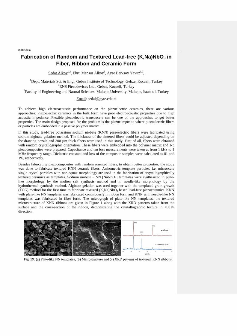
ISAF2-G2-6 _____________________________________________________________________________________________________________________
Fabrication of Random and Textured Lead-free (K,Na)NbO3 in
Fiber, Ribbon and Ceramic Form
Sedat Alkoy1,2
, Ebru Mensur Alkoy3, Ayse Berksoy Yavuz
1,2,
1Dept. Materials Sci. & Eng., Gebze Institute of Technology, Gebze, Kocaeli, Turkey
2ENS Piezodevices Ltd., Gebze, Kocaeli, Turkey
3Faculty of Engineering and Natural Sciences, Maltepe University, Maltepe, Istanbul, Turkey
Email: [email protected]
To achieve high electroacoustic performance on the piezoelectric ceramics, there are various
approaches. Piezoelectric ceramics in the bulk form have poor electroacoustic properties due to high
acoustic impedance. Flexible piezoelectric transducers can be one of the approaches to get better
properties. The main design proposed for the problem is the piezocomposite where piezoelectric fibers
or particles are embedded in a passive polymer matrix.
In this study, lead-free potassium sodium niobate (KNN) piezoelectric fibers were fabricated using
sodium alginate gelation method. The thickness of the sintered fibers could be adjusted depending on
the drawing nozzle and 300 µm thick fibers were used in this study. First of all, fibers were obtained
with random crystallographic orientation. These fibers were embedded into the polymer matrix and 1-3
piezocomposites were prepared. Capacitance and tan loss measurements were taken at from 1 kHz to 1
MHz frequency range. Dielectric constant and loss of the composite samples were calculated as 81 and
1%, respectively.
Besides fabricating piezocomposites with random oriented fibers, to obtain better properties, the study
was done to fabricate textured KNN ceramic fibers. Anisometric template particles, i.e. microscale
single crystal particles with non-equax morphology are used in the fabrication of crsytallographically
textured ceramics as templates. Sodium niobate – NN [NaNbO3] templates were synthesized in plate-
like morphology by the molten salt synthesis method and in needle-like morphology by the
hydrothermal synthesis method. Alginate gelation was used together with the templated grain growth
(TGG) method for the first time to fabricate textured (K,Na)NbO3 based lead-free piezoceramics. KNN
with plate-like NN templates was fabricated continuously in ribbon form and KNN with needle-like NN
templates was fabricated in fiber form. The micrograph of plate-like NN templates, the textured
microstructure of KNN ribbons are given in Figure 1 along with the XRD patterns taken from the
surface and the cross-section of the ribbon, demonstrating the crystallographic texture in <001>
direction.
Fig. 59: (a) Plate-like NN templates, (b) Microstructure and (c) XRD patterns of textured KNN ribbons.
cross-section
surface

Pb-based ceramics: Domains
CLUB C
Wednesday, July 24 2013, 10:30 am - 12:00 pm
Chair: Celine Lichtensteiger
DPMC - University of Geneva
ISAF3-G3-1 _____________________________________________________________________________________________________________________
Study of Domain Structure and Phase Transitions in
Pb(Zr1-xTix)O3 Single crystals
Zuo-Guang Ye, Yujuan Xie, Alexei A. Bokov and Xifa Long
Department of Chemistry and 4D LABS, Simon Fraser University,
Burnaby, BC, V5A 1S6, Canada
Email: [email protected]
PbZr1-xTixO3 (PZT) system has been extensively studied over the past decades for both industrial
applications and fundamental research. Recently, PbZr1-xTixO3 single crystals with compositions
(0.2 ≤ x ≤ 0.65) across the mophotropic phase boundary (MPB) region have been grown in our
laboratory by a top-seeded solution growth (TSSG) technique. The availability of PZT single
crystals makes it possible to systematically investigate the correlation between structural evolution
and electrical properties in PZT system.
In this work, the domain structure and phase transitions of PZT single crystals with compositions
x=0.32, x=0.42, x=0.46 and x=0.62 are studied by polarized light microscopy (PLM),
piezoresponse force microscopy and dielectric measurements. PLM observation shows an increase
of extinction angle in the two rhombohedral crystals: x=0.32 at 340 °C, and x=0.42 at 250°C,
indicating a thermally induced polarization rotation accompanied with the rhombohedral (R) to
monoclinic (M) phase transition. The ferroelectric to paraelectric phase transition in x=0.32 is of
first order with a discontinuous change of birefringence around TC=351°C. The dielectric
measurements show anomalies below TC, confirming the R-M phase transitions in both crystals. For
the MPB composition x=0.46, PLM shows a monoclinic symmetry with complicated domain at
room temperature, which upon heating changes to a tetragonal phase at about 286°C and then to a
cubic phase at TC=394 °C. Crystals of composition x=0.46 exhibit the best piezoelectric properties,
with a piezoelectric constant d33=1223 pC/N and an electromechanical coupling factor k33=80%.
The (100) plate of the tetragonal crystal with composition x=0.62 is optically isotropic, but the
(011) plate shows a small birefringence at 45° (angle between polarizer and <100> direction). This
is because of the formation of nano-sized tetragonal domains due to the instability of the
ferroelectric phase. A total compensation is achieved in the (100) plate, but in the (011) plate the
compensation is only partial. By applying an electric field, macroscopic domains can be induced in
a (100) plate at a field of 25kV/cm and the crystal becomes anisotropic. Birefringence becomes
larger with increasing field and shows a maximum value Δn=0.012 at the field of 30kV/cm. After
the electric field is removed, the crystal changes back to isotropic, indicating the field induced
macroscopic domain is metastable. We discuss the mechanisms for the formation of domain
structures and phase transitions in PZT single crystals and compared them with the behaviour and
mechanisms of relaxor ferroelectrics.
This work is supported by the Office of Naval Research (Grants No. N00014-11-1-0552 and
N00014-12-1-1045) and the Natural Science and Engineering Research Council of Canada.
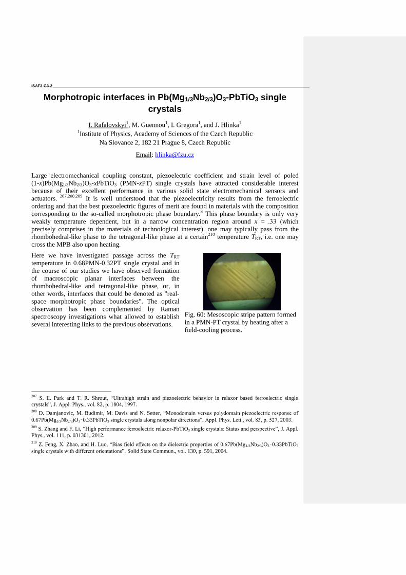
ISAF3-G3-2 _____________________________________________________________________________________________________________________
Morphotropic interfaces in Pb(Mg1/3Nb2/3)O3-PbTiO3 single
crystals
I. Rafalovskyi1, M. Guennou
1, I. Gregora
1, and J. Hlinka
1
1Institute of Physics, Academy of Sciences of the Czech Republic
Na Slovance 2, 182 21 Prague 8, Czech Republic
Email: [email protected]
Large electromechanical coupling constant, piezoelectric coefficient and strain level of poled
(1-x)Pb(Mg1/3Nb2/3)O3-xPbTiO3 (PMN-xPT) single crystals have attracted considerable interest
because of their excellent performance in various solid state electromechanical sensors and
actuators. 207,208,209
It is well understood that the piezoelectricity results from the ferroelectric
ordering and that the best piezoelectric figures of merit are found in materials with the composition
corresponding to the so-called morphotropic phase boundary.3 This phase boundary is only very
weakly temperature dependent, but in a narrow concentration region around x ≈ .33 (which
precisely comprises in the materials of technological interest), one may typically pass from the
rhombohedral-like phase to the tetragonal-like phase at a certain210
temperature TRT, i.e. one may
cross the MPB also upon heating.
Here we have investigated passage across the TRT
temperature in 0.68PMN-0.32PT single crystal and in
the course of our studies we have observed formation
of macroscopic planar interfaces between the
rhombohedral-like and tetragonal-like phase, or, in
other words, interfaces that could be denoted as "real-
space morphotropic phase boundaries". The optical
observation has been complemented by Raman
spectroscopy investigations what allowed to establish
several interesting links to the previous observations.
207
S. E. Park and T. R. Shrout, “Ultrahigh strain and piezoelectric behavior in relaxor based ferroelectric single
crystals”, J. Appl. Phys., vol. 82, p. 1804, 1997. 208
D. Damjanovic, M. Budimir, M. Davis and N. Setter, “Monodomain versus polydomain piezoelectric response of
0.67Pb(Mg1/3Nb2/3)O3–0.33PbTiO3 single crystals along nonpolar directions”, Appl. Phys. Lett., vol. 83, p. 527, 2003.
209 S. Zhang and F. Li, “High performance ferroelectric relaxor-PbTiO3 single crystals: Status and perspective”, J. Appl.
Phys., vol. 111, p. 031301, 2012.
210 Z. Feng, X. Zhao, and H. Luo, “Bias field effects on the dielectric properties of 0.67Pb(Mg1/3Nb2/3)O3–0.33PbTiO3
single crystals with different orientations”, Solid State Commun., vol. 130, p. 591, 2004.
Fig. 60: Mesoscopic stripe pattern formed
in a PMN-PT crystal by heating after a
field-cooling process.
ISAF3-G3-3 _____________________________________________________________________________________________________________________
In situ TEM on Phase Transitions in Perovskite Ceramics
Xiaoli Tan, Hanzheng Guo, Cheng Ma
Department of Materials Science and Engineering, Iowa State University, Ames, Iowa/USA
Email: [email protected]
Perovskite oxides are rich in electric field-induced phase transitions, such as the relaxor-to-
ferroelectric and antiferroelectric-to-ferroelectric ones. In this study, electric field in-situ TEM
technique is used to investigate the seemingly unlikely ferroelectric-to-relaxor and ferroelectric-to-
antiferroelectric transitions at room temperature. Specifically, antiferroelectric
Pb0.99Nb0.02[(Zr0.57Sn0.43)0.92Ti0.08]0.98O3 (PNZST43/8/2) and relaxor Pb0.92La0.08(Zr0.65Sn0.35)O3
(PLZT8/65/35) ceramics are focused in this study.
During the application of the very first cycle of electric field to these ceramics, the electric field in
the first quarter cycle transforms the antiferroelectric PNZST43/8/2 or the relaxor PLZT8/65/35
phase into a ferroelectric phase. The “induced ferroelectric phase” is metastable and its polarization
is largely preserved during the second quarter cycle. The remanent polarization is switched to the
reversed direction in the third quarter cycle when the electric field with reversed polarity increases.
The coercive field, EC, is at the intercept of the polarization curve with the electric field axis in the
third quarter cycle. Presumably, the induced metastable ferroelectric phase behaves as a normal
ferroelectric and switches its polarization through a normal domain nucleation and growth process.
However, there have been indications that this polarization reversal is quite unusual and unique
because it takes place through seemingly unlikely phase transitions at close vicinity of EC. These
reverse phase transitions produce “transient antiferroelectric” and “transient relaxor” phases during
the polarization switching process of the induced ferroelectric phase. These transient phases are
directly visualized in real time at nanometer resolution with the electric field in-situ TEM
technique.
In addition, electric field-induced phase transitions in (K0.5Na0.5)NbO3-based ceramics were also
investigated with the in situ TEM technique.
ISAF3-G3-4 _____________________________________________________________________________________________________________________
Heat treatment effects on domain configuration and strain
behavior under electric field in undoped Pb[ZrxTi1-x]O3
ferroelectrics
Ljubomira Ana Schmitt1, Hans Kungl
2, Manuel Hinterstein
3, Hans-Joachim Kleebe
1,
Michael J. Hoffmann2, Hartmut Fuess
1
1Institute of Materials and Geo-Sciences, Technische Universität Darmstadt,
64287 Darmstadt, Germany 2Institute for Ceramics and Mechanical Engineering, Karlsruhe Institute of Technology,
76131 Karlsruhe, Germany 3Institut für Werkstoffwissenschaften, Technische Universität Dresden,
01062 Dresden, Germany
Email: [email protected]
Undoped Pb [ZrxTi1-x]O3 (PZT) ceramics with Zr/Ti ratios 52/48, 52.5/47.5, 56/44 and 57.5/42.5
from the tetragonal and the rhombohedral side of the morphotropic phase boundary were examined.
Effects of heat treatments below and slightly above Curie temperature on domain configuration and
strain behavior were investigated.
Changes in domain configuration during the heating cycles were observed by in situ hot-stage
transmission electron microscopy1. After cooling down, the domain configurations do not
immediately return to their initial shape. However, after exposure at ambient temperature conditions
for 96 h, they redevelop to a state largely similar to the initial configuration. During the transient
post annealing state, changes in the strain behavior under electric field were found, when comparing
the strain behavior of non-heat treated and heat treated ceramics right after cooling. The enhanced
response to 4 kV/mm electric fields results in qualitatively different effects for PZT from the
tetragonal side and from the rhombohedral side of the morphotropic phase boundary.
Overall the experiments show that after annealing the domain configuration is reversible, but time is
required to return to the initial patterns. During the transient non equilibrium state, enhanced
influence of electric field was detected, which may show up in different forms, depending on the
material and the level of the electric fields applied.

1 L. A. Schmitt, R. Theissmann, J. Kling, H. Kungl, M. J. Hoffmann and H. Fuess “In situ hot-stage transmission
electron microscopy of Pb(Zr0.52Ti0.48)O3”, Phase Transitions, vol. 81, p. 323-329, 2008.
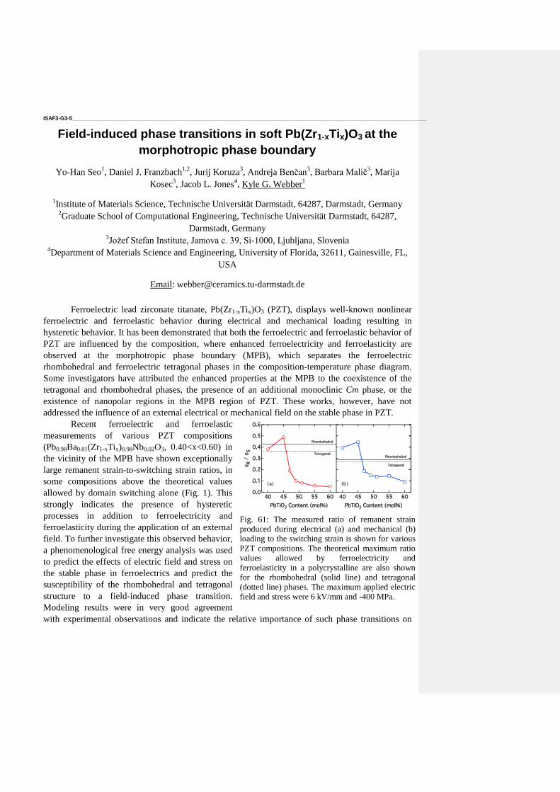
ISAF3-G3-5 _____________________________________________________________________________________________________________________
Field-induced phase transitions in soft Pb(Zr1-xTix)O3 at the
morphotropic phase boundary
Yo-Han Seo1, Daniel J. Franzbach
1,2, Jurij Koruza
3, Andreja Benčan
3, Barbara Malič
3, Marija
Kosec3, Jacob L. Jones
4, Kyle G. Webber
1
1Institute of Materials Science, Technische Universität Darmstadt, 64287, Darmstadt, Germany 2Graduate School of Computational Engineering, Technische Universität Darmstadt, 64287,
Darmstadt, Germany 3Jožef Stefan Institute, Jamova c. 39, Si-1000, Ljubljana, Slovenia
4Department of Materials Science and Engineering, University of Florida, 32611, Gainesville, FL,
USA
Email: [email protected]
Ferroelectric lead zirconate titanate, Pb(Zr1-xTix)O3 (PZT), displays well-known nonlinear
ferroelectric and ferroelastic behavior during electrical and mechanical loading resulting in
hysteretic behavior. It has been demonstrated that both the ferroelectric and ferroelastic behavior of
PZT are influenced by the composition, where enhanced ferroelectricity and ferroelasticity are
observed at the morphotropic phase boundary (MPB), which separates the ferroelectric
rhombohedral and ferroelectric tetragonal phases in the composition-temperature phase diagram.
Some investigators have attributed the enhanced properties at the MPB to the coexistence of the
tetragonal and rhombohedral phases, the presence of an additional monoclinic Cm phase, or the
existence of nanopolar regions in the MPB region of PZT. These works, however, have not
addressed the influence of an external electrical or mechanical field on the stable phase in PZT.
Recent ferroelectric and ferroelastic
measurements of various PZT compositions
(Pb0.98Ba0.01(Zr1-xTix)0.98Nb0.02O3, 0.40<x<0.60) in
the vicinity of the MPB have shown exceptionally
large remanent strain-to-switching strain ratios, in
some compositions above the theoretical values
allowed by domain switching alone (Fig. 1). This
strongly indicates the presence of hysteretic
processes in addition to ferroelectricity and
ferroelasticity during the application of an external
field. To further investigate this observed behavior,
a phenomenological free energy analysis was used
to predict the effects of electric field and stress on
the stable phase in ferroelectrics and predict the
susceptibility of the rhombohedral and tetragonal
structure to a field-induced phase transition.
Modeling results were in very good agreement
with experimental observations and indicate the relative importance of such phase transitions on
Fig. 61: The measured ratio of remanent strain
produced during electrical (a) and mechanical (b)
loading to the switching strain is shown for various
PZT compositions. The theoretical maximum ratio
values allowed by ferroelectricity and
ferroelasticity in a polycrystalline are also shown
for the rhombohedral (solid line) and tetragonal
(dotted line) phases. The maximum applied electric
field and stress were 6 kV/mm and -400 MPa.

macroscopic behavior, giving an indirect method to observe field-induced phase transitions in
polycrystalline ferroelectrics.
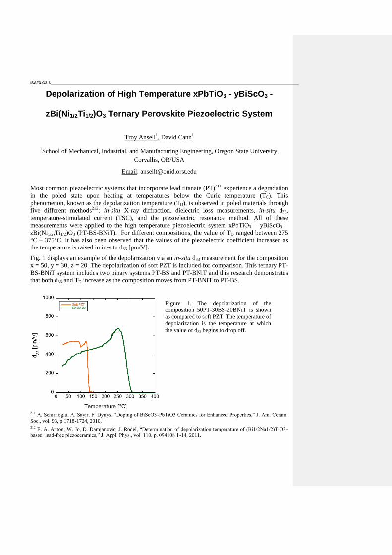
ISAF3-G3-6 _____________________________________________________________________________________________________________________
Depolarization of High Temperature xPbTiO3 - yBiScO3 -
zBi(Ni1/2Ti1/2)O3 Ternary Perovskite Piezoelectric System
Troy Ansell1, David Cann
1
1School of Mechanical, Industrial, and Manufacturing Engineering, Oregon State University,
Corvallis, OR/USA
Email: [email protected]
Most common piezoelectric systems that incorporate lead titanate (PT)211
experience a degradation
in the poled state upon heating at temperatures below the Curie temperature (TC). This
phenomenon, known as the depolarization temperature (TD), is observed in poled materials through
five different methods212
: in-situ X-ray diffraction, dielectric loss measurements, in-situ d33,
temperature-stimulated current (TSC), and the piezoelectric resonance method. All of these
measurements were applied to the high temperature piezoelectric system xPbTiO3 – yBiScO3 –
zBi(Ni1/2,Ti1/2)O3 (PT-BS-BNiT). For different compositions, the value of TD ranged between 275
°C – 375°C. It has also been observed that the values of the piezoelectric coefficient increased as
the temperature is raised in in-situ d33 [pm/V].
Fig. 1 displays an example of the depolarization via an in-situ d33 measurement for the composition
x = 50, y = 30, z = 20. The depolarization of soft PZT is included for comparison. This ternary PT-
BS-BNiT system includes two binary systems PT-BS and PT-BNiT and this research demonstrates
that both d33 and TD increase as the composition moves from PT-BNiT to PT-BS.
211
A. Sehirlioglu, A. Sayir, F. Dynys, “Doping of BiScO3-PbTiO3 Ceramics for Enhanced Properties,” J. Am. Ceram.
Soc., vol. 93, p 1718-1724, 2010. 212
E. A. Anton, W. Jo, D. Damjanovic, J. Rödel, “Determination of depolarization temperature of (Bi1/2Na1/2)TiO3-
based lead-free piezoceramics,” J. Appl. Phys., vol. 110, p. 094108 1-14, 2011.
Figure 1. The depolarization of the
composition 50PT-30BS-20BNiT is shown
as compared to soft PZT. The temperature of
depolarization is the temperature at which
the value of d33 begins to drop off.

Pb-free film processing
CLUB A
Wednesday, July 24 2013, 02:00 pm - 03:30 pm
Chair: Jon Ihlefeld
Sandia National Laboratories
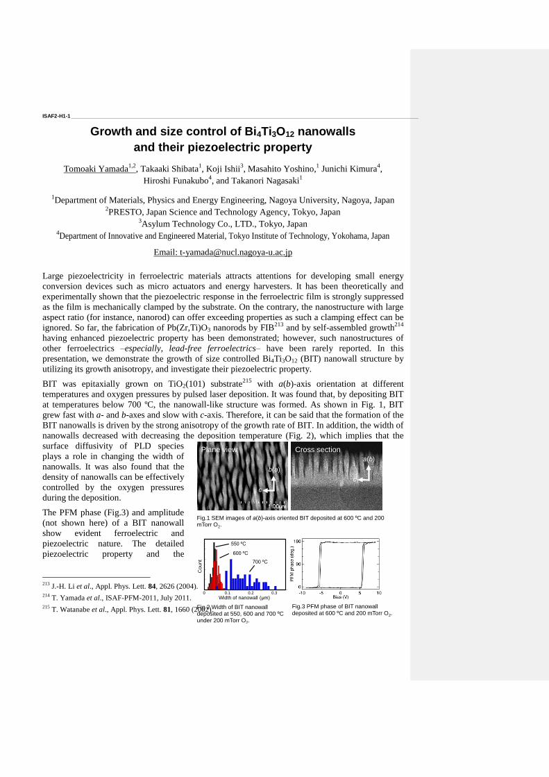
ISAF2-H1-1 _____________________________________________________________________________________________________________________
Growth and size control of Bi4Ti3O12 nanowalls
and their piezoelectric property
Tomoaki Yamada1,2
, Takaaki Shibata1, Koji Ishii
3, Masahito Yoshino,
1 Junichi Kimura
4,
Hiroshi Funakubo4, and Takanori Nagasaki
1
1Department of Materials, Physics and Energy Engineering, Nagoya University, Nagoya, Japan
2PRESTO, Japan Science and Technology Agency, Tokyo, Japan
3Asylum Technology Co., LTD., Tokyo, Japan
4Department of Innovative and Engineered Material, Tokyo Institute of Technology, Yokohama, Japan
Email: [email protected]
Large piezoelectricity in ferroelectric materials attracts attentions for developing small energy
conversion devices such as micro actuators and energy harvesters. It has been theoretically and
experimentally shown that the piezoelectric response in the ferroelectric film is strongly suppressed
as the film is mechanically clamped by the substrate. On the contrary, the nanostructure with large
aspect ratio (for instance, nanorod) can offer exceeding properties as such a clamping effect can be
ignored. So far, the fabrication of Pb(Zr,Ti)O3 nanorods by FIB213
and by self-assembled growth214
having enhanced piezoelectric property has been demonstrated; however, such nanostructures of
other ferroelectrics –especially, lead-free ferroelectrics– have been rarely reported. In this
presentation, we demonstrate the growth of size controlled Bi4Ti3O12 (BIT) nanowall structure by
utilizing its growth anisotropy, and investigate their piezoelectric property.
BIT was epitaxially grown on TiO2(101) substrate215
with a(b)-axis orientation at different
temperatures and oxygen pressures by pulsed laser deposition. It was found that, by depositing BIT
at temperatures below 700 ºC, the nanowall-like structure was formed. As shown in Fig. 1, BIT
grew fast with a- and b-axes and slow with c-axis. Therefore, it can be said that the formation of the
BIT nanowalls is driven by the strong anisotropy of the growth rate of BIT. In addition, the width of
nanowalls decreased with decreasing the deposition temperature (Fig. 2), which implies that the
surface diffusivity of PLD species
plays a role in changing the width of
nanowalls. It was also found that the
density of nanowalls can be effectively
controlled by the oxygen pressures
during the deposition.
The PFM phase (Fig.3) and amplitude
(not shown here) of a BIT nanowall
show evident ferroelectric and
piezoelectric nature. The detailed
piezoelectric property and the
213
J.-H. Li et al., Appl. Phys. Lett. 84, 2626 (2004). 214
T. Yamada et al., ISAF-PFM-2011, July 2011. 215
T. Watanabe et al., Appl. Phys. Lett. 81, 1660 (2002).
Fig.1 SEM images of a(b)-axis oriented BIT deposited at 600 ºC and 200 mTorr O2.
b(a)
c
a(b)
c
Plane view Cross section
Fig.3 PFM phase of BIT nanowall deposited at 600 ºC and 200 mTorr O2.
Fig.2 Width of BIT nanowall deposited at 550, 600 and 700 ºC under 200 mTorr O2.
0.0 0.1 0.2 0.3 0.4 0.5
Coun
t
Nanoplate width ( m)0 0.1 0.2 0.3
Cou
nt
Width of nanowall (µm)
700 ºC
550 ºC
600 ºC

comparison with the different size of nanowalls are presented.
ISAF2-H1-2 _____________________________________________________________________________________________________________________
Processing and Ferroelectric Properties of undoped and Mn-doped
x[Bi0.5Na0.5TiO3]-(1-x)[Bi0.5K0.5TiO3]-(0.04) [Bi0.5Li0.5TiO3] Thin films
M. Hejazi, A. Safari
Glenn Howatt Electroceramics Laboratory
Department of Materials Science and Engineering, Rutgers University
607 Taylor Rd, Piscataway, NJ 08854
Lead free thin films with different compositions Bi0.5(Na0.76K0.2Li0.04)0.5TiO3 (BNKLT76)
and Bi0.5(Na0.88K0.08Li0.04)0.5TiO3 (BNKLT88) were deposited on SrRuO3 coated (001)-SrTiO3
substrates by pulsed laser deposition technique. The effects of oxygen pressure and Mn-doping on
the leakage current, ferroelectric and dielectric properties were investigated. It was found that
polarization and permittivity of BNKLT76 composition is higher than those of BNKLT88 thin
films. However, it suffers from high dielectric loss and leakage current. To improve the insulating
properties, ceramic targets were doped with 2 mol.% Mn. The remnant polarization and dielectric
constant (at 10 kHz) of Mn-doped BNKLT76 film deposited at 400 mtorr were measured to be 23
µC.cm-2
and 660, respectively. The leakage current density of Mn-doped films was suppressed by
more than two orders of magnitude and the polarization was considerably enhanced. It was also
demonstrated that Mn doping decreases the dielectric loss without any adverse effect on
permittivity. The XPS results showed coexistence of Mn2+
, Mn3+
, and Mn4+
in doped-films.
Oxidation of Mn2+
to higher valence states by absorbing holes along with occupation of A-site
vacancies might be possible reasons for a reduced leakage current and dielectric loss in Mn-doped
films.
ISAF2-H1-3 _____________________________________________________________________________________________________________________
Bi-based Piezoelectric Thin Films via Chemical Solution
Deposition
Yu Hong Jeon1, Eric Patterson
2, David P. Cann
1, Peter Mardilovich
3, William Stickle
3, and Brady J.
Gibbons1
1Materials Science, School of Mechanical, Industrial, & Manufacturing Engineering, Oregon State
University, Corvallis, OR 97331 (USA) 2Institute of Materials Science, Technische Universität Darmstadt, Darmstadt, 64287, Hesse,
Germany 3Hewlett-Packard Corporation, Corvallis, OR 97330 (USA)
Email: [email protected]
The highest performing piezoelectric materials include lead as a major constituent. Worldwide,
increased restrictions on the use of lead have resulted in a search for candidates to replace these
lead-based piezoelectric materials. One promising material is the solid solution of (Bi0.5Na0.5)TiO3
– (Bi0.5K0.5)TiO3 (BNT-BKT). Although promising behavior has been observed in bulk materials,
similar results have been elusive for BNT-BKT thin films. In this work, 0.8 BNT – 0.2 BKT thin
films (near morphotropic phase boundary composition) were synthesized on platinized silicon
substrates via chemical solution deposition. Well-crystallized BNT – BKT thin films were grown at
varying processing conditions. Phase purity was confirmed by X-ray diffraction. As Bi, Na, and K
are volatile elements, overdoping of these cations (addition of excess cation precursors) was
introduced to compensate for volatilization during synthesis. Quantitative compositional analysis of
films was performed with electron probe microanalysis and compositional depth profiling to
confirm atomic ratios via X-ray photoelectron spectroscopy. The composition data from both
measurements were consistent and indicated stoichiometric films were achieved. Dependent on the
overdoping and annealing conditions, dense, smooth, crack-free films were achieved with relative
dielectric constants from 390 to 730 and low
dielectric loss of 2 - 5% at 1 kHz. Additionally,
maximum and remanent polarizations of 45 and 16
µC/cm2, respectively, were recorded at 200 Hz. The
addition of Bi(Mg0.5Ti0.5)O3 (BMgT) was also
explored, as promising piezoelectric response (high
field d33 up to 600 pm/V) in bulk compositions has
been observed. BNT-BKT-BMgT thin films were
prepared, showing very promising piezoelectric
response with d33,f up to 75 pm/V and strain values up
to 0.35%, as measured by double beam interferometry
(see Fig. 1, with values compared to typical Pb-based
thin films).216
Finally, Rayleigh analysis was
completed on several Bi-based thin film compositions
216
Y-H. Jeon, et al. “Large piezoresponse and ferroelectric properties of (Bi0.5Na0.5)TiO3 – (Bi0.5K0.5)TiO3 –
Bi(Mg0.5Ti0.5)O3 thin films prepared by chemical solution deposition,” J. Am. Ceram. Soc., in press.
-0.1
0
0.1
0.2
0.3
0.4
0.5
0.6
-500 -250 0 250 500
BNT-BKT-BMgTBNT-BKT-BMgTPZTPZT
Field [kV/cm]
Str
ain
[%
]
Figure 62: Strain measurements of BNT-
BKT-BMgT thin films compared to typical
lead zirconate titanate (52/48) solution
derived thin films.

to extract the intrinsic and extrinsic contributions to the dielectric properties.
ISAF2-H1-4 _____________________________________________________________________________________________________________________
Realization and characterization of manganese-doped BST thin
films for reflect array applications
Hartmut W. Gundel1, Kevin Nadaud
1, Caroline Borderon
1, Sabrina Pavy
1, Raphaël Gillard
2
1IETR, University of Nantes, Nantes, France
2IETR, INSA of Rennes, Rennes, France
E-mail: [email protected]
Ferroelectric thin films are attractive materials for tunable microwave devices such as electrically
tunable filters, reflect arrays, resonators or phase shifters. For this type of application, the
ferroelectric material should have an important tunability of the dielectric permittivity and low
dielectric losses. It is well known that the dielectric properties strongly depend on the material’s
microstructure and that they are particularly sensitive to existing defects. In perovskite type
ferroelectric thin films, oxygen vacancies play an important role as these defects create conduction
in the film and losses may be important; hence it becomes necessary to dope the film in order to
reduce the influence of the defects.
Mn-doped Ba(1-x)SrxTiO3 (BST) thin films already have been realized by Chemical Solution
Deposition (CSD) on stainless steel substrates217
and the influence of its morphology on the
dielectric properties has been shown218
. Ba(1-x)SrxTiO3 is a mixed compound of BaTiO3 and SrTiO3
which is widely studied because its Curie temperature depends on the ratio between barium and
strontium in the material. This allows tailoring the material for a use at room temperature either in
the ferroelectric or in the paraelectric phase.
In the present work, Mn-doped Ba0,80Sr0,20TiO3 (BST) thin films were realized by Chemical
Solution Deposition (CSD) on alumina as the foreseen application for a reflect array needs
integration of the ferroelectric on an insulating substrate. This allows utilization of the tunable
dielectric permittivity in a CoPlanar Waveguide (CPW) technology.
In order to compensate the electrons released by the oxygen vacancies, we have studied manganese
doping which acts as an electron acceptor, substituting the titanium ions. As the optimum dopant
rate to be inserted depends on the material’s defect density, we have investigated BST doping with
a manganese content ranging from 0% to 2%. The dielectric and electrical characteristics were
investigated as a function of Mn content in the frequency range of 100 Hz to 10 GHz Depending on
the expected application, a compromise between high tunability and low dielectric losses thus can
be established by using the appropriate amount of the dopant. .
217
C. Borderon, D. Averty, R. Seveno, H.W. Gundel, "Preparation and characterization of barium strontium titanate
thin films by chemical solution deposition", Ferroelectrics 362 (2008) 1-7 218
C. Borderon, D. Averty, R. Seveno, H.W. Gundel, "Influence of the morphology of Barium Strontium Titanate thin
films on the ferroelectric and dielectric properties", Integrated Ferroelectrics 97 (2008) 12-19
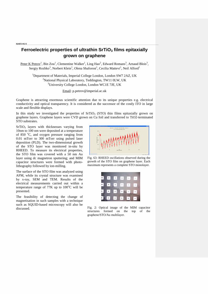
ISAF2-H1-5 _____________________________________________________________________________________________________________________
Ferroelectric properties of ultrathin SrTiO3 films epitaxially
grown on graphene
Peter K Petrov1, Bin Zou
1, Clementine Walker
1, Ling Hao
2, Edward Romans
3, Arnaud Blois
3,
Sergiy Rozhko3, Norbert Klein
1, Olena Shaforost
1, Cecilia Mattevi
1, Neil Alford
1
1Department of Materials, Imperial College London, London SW7 2AZ, UK
2National Physical Laboratory, Teddington, TW11 0LW, UK
3University College London, London WC1E 7JE, UK
Email: [email protected]
Graphene is attracting enormous scientific attention due to its unique properties e.g. electrical
conductivity and optical transparency. It is considered as the successor of the costly ITO in large
scale and flexible displays.
In this study we investigated the properties of SrTiO3 (STO) thin films epitaxially grown on
graphene layers. Graphene layers were CVD grown on Cu foil and transferred to TiO2-terminated
STO substrates.
SrTiO3 layers with thicknesses varying from
10nm to 100 nm were deposited at a temperature
of 850 oC, and oxygen pressure ranging from
0.01 mTorr to 300 mTorr using pulsed laser
deposition (PLD). The two-dimensional growth
of the STO layer was monitored in-situ by
RHEED. To measure its electrical properties,
the STO film was covered with a 50 nm Au
layer using dc magnetron sputtering; and MIM
capacitor structures were formed with photo-
lithography followed by ion-milling.
The surface of the STO film was analyzed using
AFM, while its crystal structure was examined
by x-ray, SEM and TEM. Results of the
electrical measurements carried out within a
temperature range of 77K up to 100oC will be
presented.
The feasibility of detecting the change of
magnetisation in such samples with a technique
such as SQUID-based microscopy will also be
discussed.
Fig. 63: RHEED oscillations observed during the
growth of the STO film on graphene layer. Each
maximum represents a complete STO monolayer.
Fig. 2: Optical image of the MIM capacitor
structures formed on the top of the
graphene/STO/Au multilayer.
ISAF2-H1-6 _____________________________________________________________________________________________________________________
Solgel Hydrothermal Synthesis of BaTiO3/MWCNTs for Microelectronic Applications
Amit Mahajan1, Paula M. Vilarinho
1, Angus Kingon
2 and Ákos Kukovecz
3,4
1Department of Materials and Ceramic Engineering, CICECO, University of Aveiro, 3810-193
Aveiro, Portugal 2Division of Engineering, Brown University, Providence, Rhode Island 02912, USA
3Department of Applied and Environmental Chemistry, Faculty of Sciences, University of Szeged,
H-6720 Szeged, Hungary
and 4MTA-SZTE “Lendület” Porous Nanocomposites Research Group, 6720 Szeged, Rerrich Béla tér 1.
Email: [email protected]
CNTs have a unique set of mechanical, chemical and electrical properties which make them very
promising for the development of nanostructures and nanocomposites. In particular the ballistic
electron transport and a huge current - carrying capacity, are of interest for the many future
microelectronics applications such as super capacitors, FET and memory cells 1. Therefore, carbon
nanotubes (CNTs) is an interesting option under consideration to be used as templates or bottom
electrodes for 3D structures and used as metal filler in polymer and/or Ferroelectric (FE) in order to
improve the electrical properties 2. In the last decades, efforts have been carried out in order to
cover MWCNTs with various FE by physical vapor deposition and chemical methods to fabricate
3D capacitor structures 2-4
. Covering CNTs with FE is not a trivial task and many aspects are still
unexploited and unclear. Therefore, in this work systematic studies were carried out for the
fabrication by a sol gel hydrothermal method of BT/MWCNTs composites and measurement of
electrical properties.
Functionalized MWCNTs with HNO3 were used, having diameter and length around 10-35 nm and
~10 µm, respectively. Barium titanate solution was prepared from barium acetate and titanium
isopropoxide precursor. In the BT solution, MWCNTs were dispersed for five minutes using ultra
high -sonication followed by 2 h stirring. Potassium hydroxide solution was added in to BT-
MWCNTs solution, in order to precipitate BT. The precipitated slurry was transfer to the autoclave
and the hydrothermal reaction was carried out from 2 to 24 h and temperatures ranging from 100 to
250 ºC to obtained BT-MWCNTs composites. Pure BT powder was also synthesis using similar
process for comparison. The composite were characterized by XRD, FTIR, Raman and Electron
Microscopy for phase formation and morphology of the composites. The electrical properties were
measured using Piezo Force Microscope (PFM) and Impedance spectroscopy.

Novel Ferroelectric Devices
CLUB B
Wednesday, July 24 2013, 02:00 pm - 03:30 pm
Chair: Glen Fox
Fox Materials Consulting
ISAF4-H2-1 _____________________________________________________________________________________________________________________
Planar Laser-Micro Machined Bulk PZT Bimorph For
In-Plane Actuation
Sachin Nadig1, Serhan Ardanuç
2, Victor Haas
3, Amit Lal
4
1Electrical And Computing Engineering, Cornell University, Ithaca, NY 14853,USA
Email: [email protected]
In this work, we demonstrate a PZT bimorph technology for high level chip-scale nano-motion
actuator integration. Precision piezoelectric stages for linear and rotary motion have proven to be of
great value in areas that require accurate positioning and calibration. Ultrasonic motors and
piezoelectric actuators such as bimorphs, unimorphs and shear tubes are key elements of these
systems. Bimorphs are the most commonly used actuators to maximize displacement. Most
bimorphs are macro scale, millimeters in thickness and centimeters in width and length, making it
unsuitable for integration in microsystems. Manual assembly of many of these large devices is
required for large displacements and this does not lead to small systems. Alternatively, thin film
MEMS unimorphs and bimorphs use microns of piezoelectric material (PZT, AlN, ZnO) that
generally produce out of plane motion. A miniature bimorph technology that enables many
bimorphs to be placed in precision and provide lateral in-plane motion, with single direction of
polarization is not available. In this work, we present experimental results on a bimorph fabricated
from bulk PZT 4H by laser cutting of PZT plates.
The actuators were fabricated using a commercial laser cutting tool to define beams by cutting
entirely through the PZT plate. The laser cutting tool is also used to define arbitrary two-
dimensional electrode patterns on the PZT beam. A 10mm long, 0.45mm wide and 0.5mm thick
PZT 4H actuator was tested with actuation capabilities of ~ 0.08µm/V for single side and ~
0.18µm/V for double sided electrode patterns. Figure 1 shows the process flow and the fabricated
bimorph.
Our demonstrated actuator can be useful in low-cost miniature precision nano-motion stages for
manipulating MEMS devices. The laser cutting enables a repeatable, high-throughput fabrication
process, which creates devices that are capable of larger displacements than conventional bimorphs.
While we demonstrate the process on a planar bimorph structure, this also allows fabrication of 3D
piezoelectric actuators with arbitrary electrode patterns, allowing engineering of complex
displacement profiles.
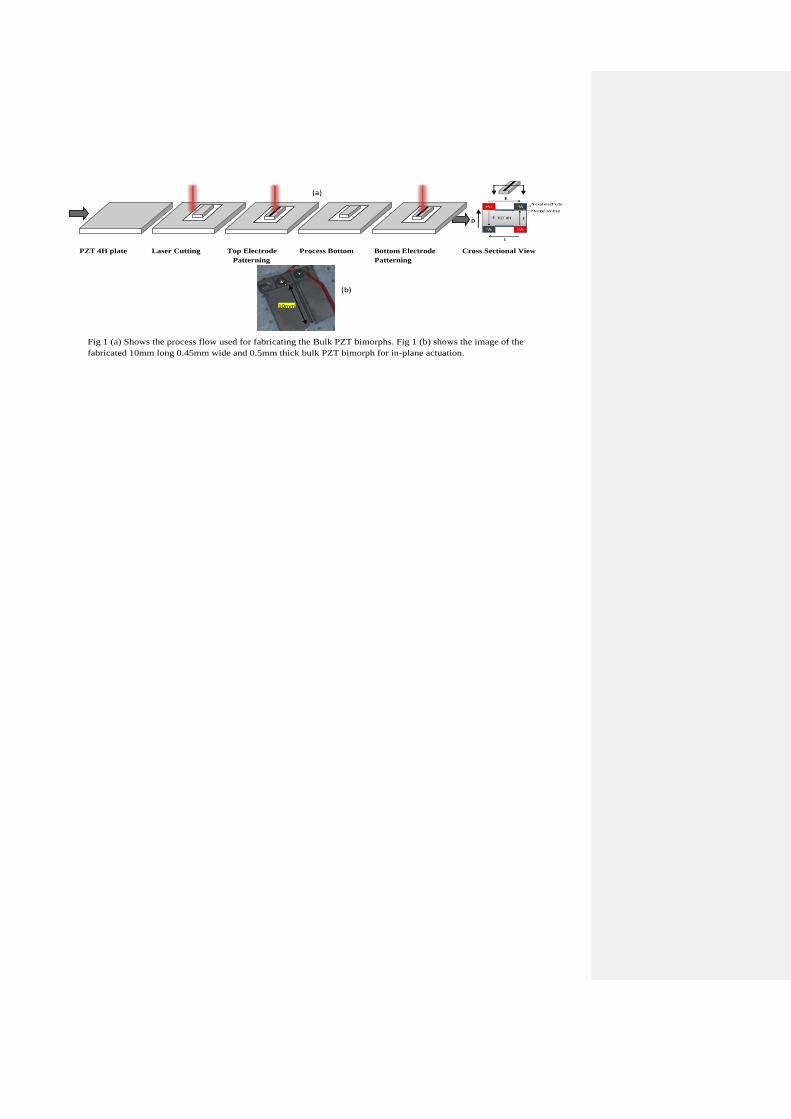
P
PZT 4H plate Laser Cutting Top Electrode Process Bottom Bottom Electrode Cross Sectional View
Patterning Patterning
10mm
Fig 1 (a) Shows the process flow used for fabricating the Bulk PZT bimorphs. Fig 1 (b) shows the image of the
fabricated 10mm long 0.45mm wide and 0.5mm thick bulk PZT bimorph for in-plane actuation.
(a)
(b)
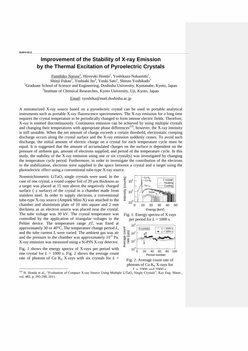
ISAF4-H2-2 _____________________________________________________________________________________________________________________
Improvement of the Stability of X-ray Emission
by the Thermal Excitation of Pyroelectric Crystals
Fumihiko Naruse1, Hiroyuki Honda
1, Yoshikazu Nakanishi
1,
Shinji Fukao1, Yoshiaki Ito
2, Yuuki Sato
1, Shinzo Yoshikado
1
1Graduate School of Science and Engineering, Doshisha University, Kyotanabe, Kyoto, Japan
2Institute of Chemical Researches, Kyoto University, Uji, Kyoto, Japan
Email: [email protected]
A miniaturized X-ray source based on a pyroelectric crystal can be used in portable analytical
instruments such as portable X-ray fluorescence spectrometers. The X-ray emission for a long time
requires the crystal temperature to be periodically changed to form intense electric fields. Therefore,
X-ray is emitted discontinuously. Continuous emission can be achieved by using multiple crystals
and changing their temperatures with appropriate phase differences219
, however, the X-ray intensity
is still unstable. When the net amount of charge exceeds a certain threshold, electrostatic creeping
discharge occurs along the crystal surface and the X-ray emission suddenly ceases. To avoid such
discharge, the initial amount of electric charge on a crystal for each temperature cycle must be
equal. It is suggested that the amount of accumulated charges on the surface is dependent on the
pressure of ambient gas, amount of electrons supplied, and period of the temperature cycle. In this
study, the stability of the X-ray emission using one or six crystal(s) was investigated by changing
the temperature cycle period. Furthermore, in order to investigate the contribution of the electrons
to the stabilization, electrons were supplied to the space between a crystal and a target using the
photoelectric effect using a conventional tube-type X-ray source.
Nonstoichiometric LiTaO3 single crystals were used. In the
case of one crystal, a round copper foil of 20 μm thickness as
a target was placed at 15 mm above the negatively charged
surface (–z surface) of the crystal in a chamber made from
stainless steel. In order to supply electrons, a conventional
tube-type X-ray source (Amptek Mini-X) was attached to the
chamber and aluminium plate of 10 mm square and 2 mm
thickness as an electron source was placed near the crystal.
The tube voltage was 30 kV. The crystal temperature was
controlled by the application of triangular voltages to the
Peltier device. The temperature range ΔT, was fixed at
approximately 30 or 40°C. The temperature change period L,
and the tube current I, were varied. The ambient gas was air
and the pressure in the chamber was approximately 10-4
Pa.
X-ray emission was measured using a Si-PIN X-ray detector.
Fig. 1 shows the energy spectra of X-rays per period with
one crystal for L = 1000 s. Fig. 2 shows the average count
rate of photons of Cu Kα X-rays with six crystals for L =
219
H. Honda et al., “Evaluation of Compact X-ray Source Using Multiple LiTaO3 Single Crystals”, Key Eng. Mater.,
vol. 485, p. 295-298, 2011.
100
102
104
Inte
nsity [
cou
nts
]
50403020100
Energy [keV]
Cu KCu K
Ta L
Noise
1 crystal Heating Cooling
Fig. 1: Energy spectra of X-rays
per period for L = 1000 s.
100
101
102
103
100806040200
Period number
Avera
ge
co
un
tra
te [
cp
s]
L = 1000 s
L = 2000 s
6 crystals
Fig. 2: Average count rate of
photons of Cu Kα X-rays for
L = 1000 and 2000 s.

1000 and 2000 s. The long-term stability of the X-ray emission was significantly changed when L
was varied.

ISAF4-H2-3 _____________________________________________________________________________________________________________________
New Cooling Technologies based on the Electrocalorics
Brigita Rožič1,2
, Zdravko Kutnjak1,2,3
, George Cordoyiannis1,2,4
, Maja Trček1, Hana Uršič
1,2, Jurij
Koruza1,2,3
, Marko Vrabelj1,3
, Barbara Malič1,2,3
, Raša Pirc1, S.-G. Lu
5, Qiming M. Zhang
5
1 Jožef Stefan Institute, Jamova cesta 39, 1001 Ljubljana, Slovenia
2 Centre of Excellence Namaste, Jamova cesta 39, 1001 Ljubljana, Slovenia
3 Jožef Stefan International Postgraduate School, Jamova cesta 39, 1001 Ljubljana, Slovenia
4 Department of Physics, University of Athens, 15784 Athens, Greece
5 Material Research Institute, the Pennsylvania State University, University Park, PA 16802, USA
Email: [email protected]
Electrocalorics, materials that exhibit a temperature change under the adiabatically applied/removed
electric field, i.e., the electrocaloric effect (ECE), are very important for more energy efficient and
environmentally acceptable technologies. An increasing interest in the research of these materials
has been revived recently by the predictions of the giant electrocaloric response in some inorganic
and organic materials220,2
.
The electrocaloric materials are, in comparison to thermoelectric or magnetocaloric materials, good
insulators and because of miniaturization possibilities they are very promising for different
applications including household refrigerators, sensors, actuators, heat pumps, devices for cooling
microelectronic components, applications in microrobotics, etc.
In this presentation a review of our direct measurements of the ECE in various inorganic and
organic bulk, thick and thin films such as relaxor ferroelectric ceramics including PMN, PMN-PT,
PLZT, KNN-STO, and thin films of normal ferroelectric and relaxor ferroelectric polymers, i.e.,
P(VDF-TrFE)-based terpolymers, copolymers and various blends3,4
will be given. Observed
magnitudes of the ECE confirm existence of the large electrocaloric effect in these systems and it
was also shown that in bulk relaxor ferroelectrics the ECE behaviour determined from the direct
measurements is in a good agreement in the vicinity of the critical point with the theoretical
predictions5.
Acknowledgment:
The contribution of Prof. Marija Kosec who passed away in December 2012 is gratefully
acknowledged.
220
A. S. Mischenko et al., “Giant electrocaloric effect in thin-film Pb0.95Ti0.05O3”, Science, vol. 311, p. 1270-1271,
2006. 2 B. Neese et al., “Large electrocaloric effect in ferroelectric polymers near room temperature”, Science, vol. 321, p.
821-823, 2008. 3 S.-G. Lu et al., “Organic and inorganic relaxor ferroelectrics with giant electrocaloric effect”, Appl. Lett. Phys., vol.
97, 162904, 2010. 4 B. Rožič et al., “Influence of the critical point on the electrocaloric response of relaxor ferroelectrics”, J. Appl. Phys.,
vol. 110, 064118, 2011. 5 R. Pirc et al., “Electrocaloric effect in relaxor ferroelectrics”, J. Appl. Phys., vol. 110, 074113, 2011.
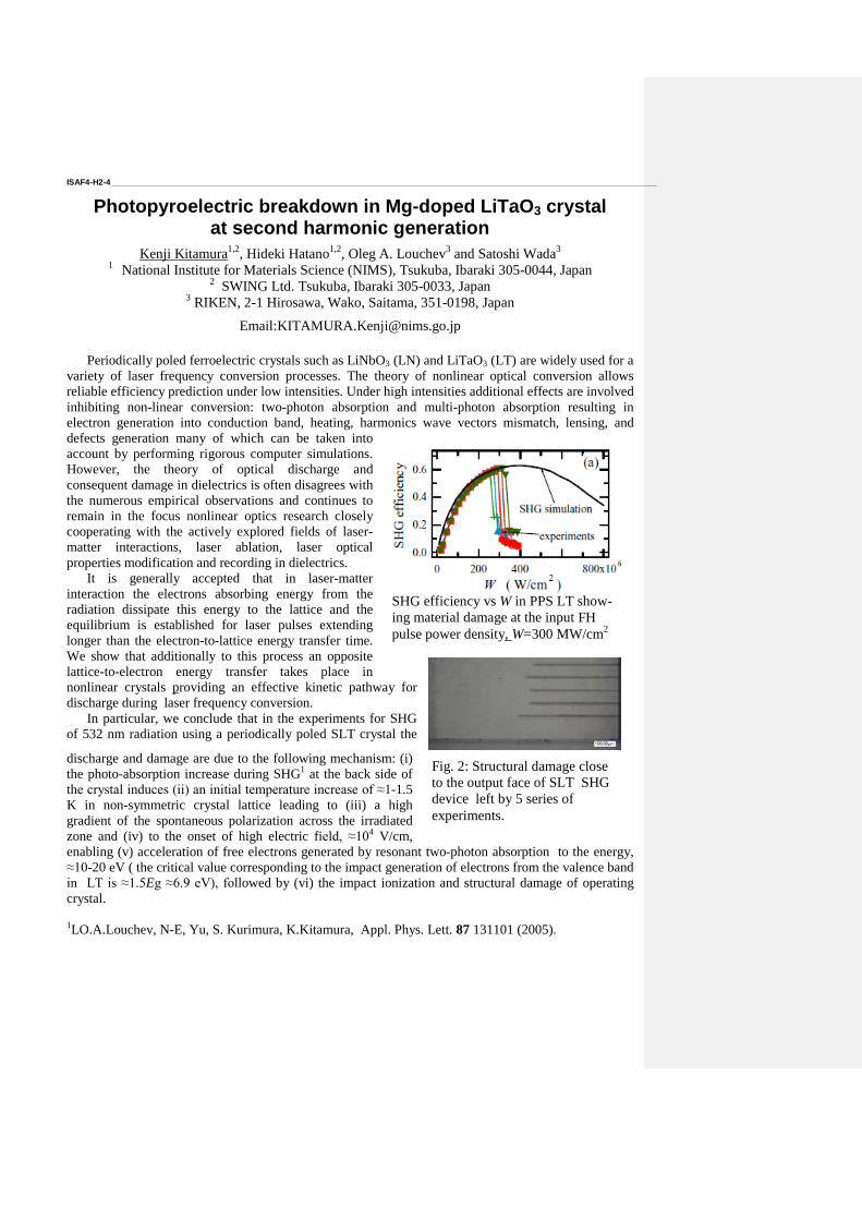
ISAF4-H2-4 _____________________________________________________________________________________________________________________
Photopyroelectric breakdown in Mg-doped LiTaO3 crystal at second harmonic generation
Kenji Kitamura1,2
, Hideki Hatano1,2
, Oleg A. Louchev3 and Satoshi Wada
3
1 National Institute for Materials Science (NIMS), Tsukuba, Ibaraki 305-0044, Japan
2 SWING Ltd. Tsukuba, Ibaraki 305-0033, Japan
3 RIKEN, 2-1 Hirosawa, Wako, Saitama, 351-0198, Japan
Email:[email protected]
Periodically poled ferroelectric crystals such as LiNbO3 (LN) and LiTaO3 (LT) are widely used for a
variety of laser frequency conversion processes. The theory of nonlinear optical conversion allows
reliable efficiency prediction under low intensities. Under high intensities additional effects are involved
inhibiting non-linear conversion: two-photon absorption and multi-photon absorption resulting in
electron generation into conduction band, heating, harmonics wave vectors mismatch, lensing, and
defects generation many of which can be taken into
account by performing rigorous computer simulations.
However, the theory of optical discharge and
consequent damage in dielectrics is often disagrees with
the numerous empirical observations and continues to
remain in the focus nonlinear optics research closely
cooperating with the actively explored fields of laser-
matter interactions, laser ablation, laser optical
properties modification and recording in dielectrics.
It is generally accepted that in laser-matter
interaction the electrons absorbing energy from the
radiation dissipate this energy to the lattice and the
equilibrium is established for laser pulses extending
longer than the electron-to-lattice energy transfer time.
We show that additionally to this process an opposite
lattice-to-electron energy transfer takes place in
nonlinear crystals providing an effective kinetic pathway for
discharge during laser frequency conversion.
In particular, we conclude that in the experiments for SHG
of 532 nm radiation using a periodically poled SLT crystal the
discharge and damage are due to the following mechanism: (i)
the photo-absorption increase during SHG1 at the back side of
the crystal induces (ii) an initial temperature increase of ≈1-1.5
K in non-symmetric crystal lattice leading to (iii) a high
gradient of the spontaneous polarization across the irradiated
zone and (iv) to the onset of high electric field, ≈104 V/cm,
enabling (v) acceleration of free electrons generated by resonant two-photon absorption to the energy,
≈10-20 eV ( the critical value corresponding to the impact generation of electrons from the valence band
in LT is ≈1.5Eg ≈6.9 eV), followed by (vi) the impact ionization and structural damage of operating
crystal.
1LO.A.Louchev, N-E, Yu, S. Kurimura, K.Kitamura, Appl. Phys. Lett. 87 131101 (2005).
Fig. 1: Experiment and simulation of
SHG efficiency vs W in PPS LT show-
ing material damage at the input FH
pulse power density, W=300 MW/cm2
Fig. 2: Structural damage close
to the output face of SLT SHG
device left by 5 series of
experiments.
ISAF4-H2-5 _____________________________________________________________________________________________________________________
Photoconductivity from Electrospun Bismuth Ferrite Nanofibers
R. Rivera, R. Kappera, M. Chhowalla and A. Safari
Department of Materials Science and Engineering
Rutgers, The State University of New Jersey, New Jersey, USA
Email: [email protected]
Bismuth ferrite (BFO) has attracted great attention not only because it is potential applications as
multiferroic material in the spintronics, and micro-electromechanical area but also because it is
photo-electronic behavior in energy harvesting field. Regardless the great interest on BFO for
ferroelectric applications there are only few studies on the photoconductivity of this material. In
this investigation we report the observation of photoconductivity from multiferroic BFO nanofibers
whose photo response varies with the diameter of the nanofiber. Bismuth ferrite nanofibers were
deposited on oxidized silicon and quartz substrates using sol-gel based electrospinning technique.
The thickness of the fibers was well controlled by varying the molarity ratio of the precursor
solution. X-ray photoelectron spectroscopy (XPS) results showed a combination of Fe3+
and Fe2+
valence states in the fibers. Rutherford backscaterring spectroscopy (RBS) result showed a
stoichiometry composition after heat treatment. Both scanning electron microscopy (SEM) and
atomic force microscopy (AFM) images revealed that the fibers structure is uniform in diameters
ranging from of 15 to 100nm and several microns in length as well. Photoconductivity
measurements show considerable increase in the current flowing through the fibers when measured
under illumination. This photoresponse behavior is almost hundred times higher for a fiber of 50nm
diameter than for a fiber of 15nm. This effect is described by a size dependent surface
recombination mechanism.
Fig. 1: Pyroelectric
detector based on
PIMNT
ISAF4-H2-6 _____________________________________________________________________________________________________________________
Application of PIN-PMN-PT:Mn in High-Performance Flame
Detectors
A. Movchikova1, N. Neumann
1
1InfraTec GmbH, Gostritzer Str. 61-63, 01217 Dresden, Germany
Email: [email protected]
Ferroelectric relaxor-PbTiO3 single crystals were reported to be the
most promising candidates for pyroelectric applications, because of
their ultra-high pyroelectric coefficient and relatively low dielectric
loss221
. In our previous works was shown that PMN-0.26PT:Mn
and PMN-0.29PT:Mn crystals, outperforms LiTaO3 (LTO) crystals
in pyroelectric detectors by a 3 times higher specific detectivity222
.
Unfortunately, rhombohedral PMNT single crystals exhibit low
phase transition temperatures (TRT≈100°C), which limit the
processing temperature during fabrication and also the operating
temperature range. Therefore, more attention is focused on the
ternary solid solution system xPIN-yPMN-(1-x-y)PT, PIMNT wich
is distinguished by a higher Curie temperature223
. In this work the suitability of Mn-doped 0.26PIN-
0.42PMN-0.32PT single crystals in single and quad channel flame detectors was evaluated and
compared with standard LTO.
The phase transitions, dielectric and pyroelectric properties of rhombohedral phase [111] oriented
0.26PIN-0.42PMN-0.32PT single crystals were investigated. InfraTec’s detector design PIE-205
operating in current mode were used for the evaluation. In addition detectors based on LiTaO3 were
prepared for an easier comparison. Responsivity and noise of both detectors were measured in the
frequency range 0.1 Hz – 10 kHz at room temperature. The specific detectivity was calculated from
signal and noise measurements (Table 1).
The evaluation shows that also Mn doped PIN-PMN-PT based detectors outperform the standard
LiTaO3 based detectors especially in the low frequency range of 1-10 Hz. Based on this basic
design a new generation of high-performance long-range flame detectors will be established.
Table 1: Material properties and detector performance of PIN-PMN-PT, LiTaO3 single crystals
Pyroelectric
material
Detector
Type
Element
Size Thickness p εr tanδ TRT TC
D* (500 K, 10 Hz, BW 1Hz, 25°C)
mm2 µm µC/m²/K (1 kHz) (1 kHz) °C °C cmHz
1/2/W
PIMNT PIE-205 2.0 x 2.0 33 730 525 0.0003 125 181 9.5 x 10⁸
LT LIE-205 2.0 x 2.0 24 175 43.5 0.0001 - 603 3.6 x 10⁸
221
Y. Tang. “Large pyroelectric response in relaxor-based ferroelectric (1-x)Pb(Mg1/3Nb2/3)O3-xPbTiO3 single crystals”,
J. Appl. Phys.,vol. 98, 084104, 2005
222 N. Neumann, M.Es-Souni, H.Luo. “Application of PMN-PT in pyroelectric detectors”, Proc ISAF-IMF-2009,
August 23-29, 2009, Xi´an, China.
223 N. Yasuda. “Crystal growth and electrical properties of lead indium niobate-lead titanate binary single crystal”, J.
Cryst. Growth, vol. 229, p.299-304, 2001.

Capacitors
CLUB C
Wednesday, July 24 2013, 02:00 pm - 03:30 pm
Chair: Satoshi Wada
University of Yamanashi
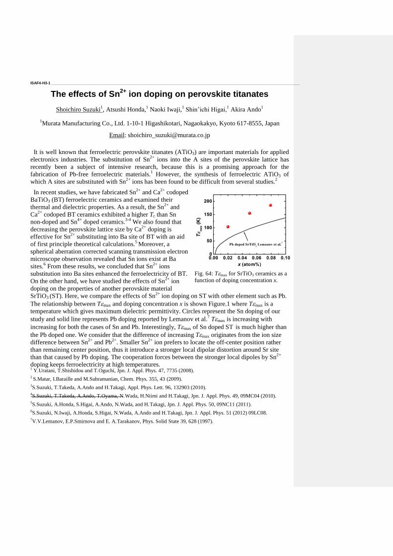
ISAF4-H3-1 _____________________________________________________________________________________________________________________
The effects of Sn2+
ion doping on perovskite titanates
Shoichiro Suzuki1, Atsushi Honda,
1 Naoki Iwaji,
1 Shin’ichi Higai,
1 Akira Ando
1
1Murata Manufacturing Co., Ltd. 1-10-1 Higashikotari, Nagaokakyo, Kyoto 617-8555, Japan
Email: [email protected]
It is well known that ferroelectric perovskite titanates (ATiO3) are important materials for applied
electronics industries. The substitution of Sn2+
ions into the A sites of the perovskite lattice has
recently been a subject of intensive research, because this is a promising approach for the
fabrication of Pb-free ferroelectric materials.1 However, the synthesis of ferroelectric ATiO3 of
which A sites are substituted with Sn2+
ions has been found to be difficult from several studies.2
In recent studies, we have fabricated Sn2+
and Ca2+
codoped
BaTiO3 (BT) ferroelectric ceramics and examined their
thermal and dielectric properties. As a result, the Sn2+
and
Ca2+
codoped BT ceramics exhibited a higher Tc than Sn
non-doped and Sn4+
doped ceramics.3-4
We also found that
decreasing the perovskite lattice size by Ca2+
doping is
effective for Sn2+
substituting into Ba site of BT with an aid
of first principle theoretical calculations.5 Moreover, a
spherical aberration corrected scanning transmission electron
microscope observation revealed that Sn ions exist at Ba
sites.6 From these results, we concluded that Sn
2+ ions
substitution into Ba sites enhanced the ferroelectricity of BT.
On the other hand, we have studied the effects of Sn2+
ion
doping on the properties of another perovskite material
SrTiO3 (ST). Here, we compare the effects of Sn2+
ion doping on ST with other element such as Pb.
The relationship between Tmax and doping concentration x is shown Figure.1 where Tmax is a
temperature which gives maximum dielectric permittivity. Circles represent the Sn doping of our
study and solid line represents Pb doping reported by Lemanov et al.7 Tmax is increasing with
increasing for both the cases of Sn and Pb. Interestingly, Tmax of Sn doped ST is much higher than
the Pb doped one. We consider that the difference of increasing Tmax originates from the ion size
difference between Sn2+
and Pb2+
. Smaller Sn2+
ion prefers to locate the off-center position rather
than remaining center position, thus it introduce a stronger local dipolar distortion around Sr site
than that caused by Pb doping. The cooperation forces between the stronger local dipoles by Sn2+
doping keeps ferroelectricity at high temperatures. 1 Y.Uratani, T.Shishidou and T.Oguchi, Jpn. J. Appl. Phys. 47, 7735 (2008).
2 S.Matar, I.Baraille and M.Subramanian, Chem. Phys. 355, 43 (2009).
3S.Suzuki, T.Takeda, A.Ando and H.Takagi, Appl. Phys. Lett. 96, 132903 (2010).
4S.Suzuki, T.Takeda, A.Ando, T.Oyama, N.Wada, H.Niimi and H.Takagi, Jpn. J. Appl. Phys. 49, 09MC04 (2010).
5S.Suzuki, A.Honda, S.Higai, A.Ando, N.Wada, and H.Takagi, Jpn. J. Appl. Phys. 50, 09NC11 (2011).
6S.Suzuki, N.Iwaji, A.Honda, S.Higai, N.Wada, A.Ando and H.Takagi, Jpn. J. Appl. Phys. 51 (2012) 09LC08.
7V.V.Lemanov, E.P.Smirnova and E. A.Tarakanov, Phys. Solid State 39, 628 (1997).
Fig. 64: Tmax for SrTiO3 ceramics as a
function of doping concentration x.
ISAF4-H3-2 _____________________________________________________________________________________________________________________
Lead free LTCC/PZT modules (LPM)
Markus Flössel1,2
, Sylvia Gebhardt2, Andreas Schönecker
2, Alexander Michaelis
1,2
1TU Dresden, Institute of Material Science, Chair of Inorganic Non-Metallic Materials, 01062
Dresden, Germany 2Fraunhofer IKTS, Winterbergstraße 28, 01277 Dresden, Germany
e-mail: [email protected]
The combination of multilayer- and piezo-technology by laminating fired lead zirconate titanate
(PZT) ceramic discs with low temperature cofired ceramics (LTCC) green layers and subsequently
sintering of the package yields to the so-called LTCC/PZT modules (LPM), which were first
published in 2010224
.
The design of the LPM can be modified and it can so be used in two different cases of application.
On one side it is used as sensor/actuator module which is metal die casted in an aluminum
component and it controls the dynamic properties (vibration damping) of thin walled devices.
Besides with this metal die casting step, batch production by combining fabrication of mechanical
components and integration of LPM in one production chain is possible. Then again it can also be
used as an ultrasonic transducer for Structural Health Monitoring (SHM) which permanently
monitors the health and condition of components used in rotorcraft, aircraft, pipelines, automobiles
et cetera.
This presentation will give an overview on technological challenges and their solution of producing
LPM and have a look of material properties and interactions especially chemical reactions in the
phase boundary of LTCC and PZT which is necessary to fabricate functional microsystems.
Regarding to the directive of the European Union 2002/95/EG and 2011/65/EU which means
restriction of the use of certain hazardous substances (RoHS) conform components, we first
developed lead free LPM and show properties of low-level signals and ferroelectric hysteresis
loops.
224
Flössel, M.; Gebhardt, S.; Schönecker, A.; Michaelis, A.: Development of a Novel Sensor-Actuator-Module with
Ceramic Multilayer Technology, In: Journal of Ceram. Sci. Tech., 01[01]55-58, 2010
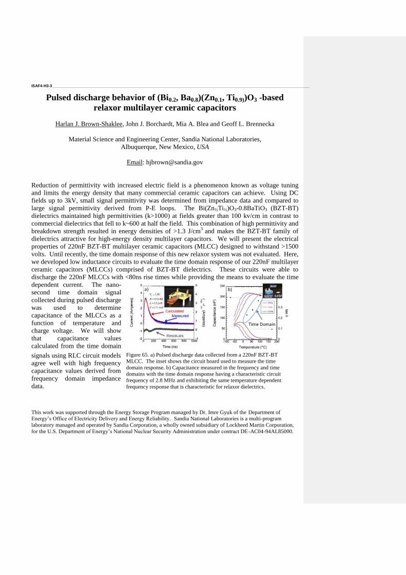
ISAF4-H3-3 _____________________________________________________________________________________________________________________
Pulsed discharge behavior of (Bi0.2, Ba0.8)(Zn0.1, Ti0.9))O3 -based
relaxor multilayer ceramic capacitors
Harlan J. Brown-Shaklee, John J. Borchardt, Mia A. Blea and Geoff L. Brennecka
Material Science and Engineering Center, Sandia National Laboratories,
Albuquerque, New Mexico, USA
Email: [email protected]
Reduction of permittivity with increased electric field is a phenomenon known as voltage tuning
and limits the energy density that many commercial ceramic capacitors can achieve. Using DC
fields up to 3kV, small signal permittivity was determined from impedance data and compared to
large signal permittivity derived from P-E loops. The Bi(Zn½Ti½)O3-0.8BaTiO3 (BZT-BT)
dielectrics maintained high permittivities (k>1000) at fields greater than 100 kv/cm in contrast to
commercial dielectrics that fell to k~600 at half the field. This combination of high permittivity and
breakdown strength resulted in energy densities of >1.3 J/cm3
and makes the BZT-BT family of
dielectrics attractive for high-energy density multilayer capacitors. We will present the electrical
properties of 220nF BZT-BT multilayer ceramic capacitors (MLCC) designed to withstand >1500
volts. Until recently, the time domain response of this new relaxor system was not evaluated. Here,
we developed low inductance circuits to evaluate the time domain response of our 220nF multilayer
ceramic capacitors (MLCCs) comprised of BZT-BT dielectrics. These circuits were able to
discharge the 220nF MLCCs with <80ns rise times while providing the means to evaluate the time
dependent current. The nano-
second time domain signal
collected during pulsed discharge
was used to determine
capacitance of the MLCCs as a
function of temperature and
charge voltage. We will show
that capacitance values
calculated from the time domain
signals using RLC circuit models
agree well with high frequency
capacitance values derived from
frequency domain impedance
data.
This work was supported through the Energy Storage Program managed by Dr. Imre Gyuk of the Department of
Energy’s Office of Electricity Delivery and Energy Reliability. Sandia National Laboratories is a multi-program
laboratory managed and operated by Sandia Corporation, a wholly owned subsidiary of Lockheed Martin Corporation,
for the U.S. Department of Energy’s National Nuclear Security Administration under contract DE-AC04-94AL85000.
Figure 65. a) Pulsed discharge data collected from a 220nF BZT-BT
MLCC. The inset shows the circuit board used to measure the time
domain response. b) Capacitance measured in the frequency and time
domains with the time domain response having a characteristic circuit
frequency of 2.8 MHz and exhibiting the same temperature dependent
frequency response that is characteristic for relaxor dielectrics.
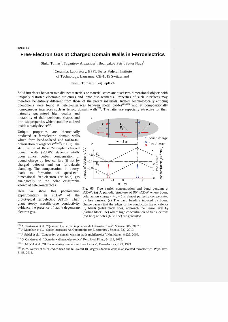
ISAF4-H3-4 _____________________________________________________________________________________________________________________
Free-Electron Gas at Charged Domain Walls in Ferroelectrics
Sluka Tomas1, Tagantsev Alexander
1, Bednyakov Petr
1, Setter Nava
1
1Ceramics Laboratory, EPFL Swiss Federal Institute
of Technology, Lausanne, CH-1015 Switzerland
Email: [email protected]
Solid interfaces between two distinct materials or material states are quasi two-dimensional objects with
uniquely distorted electronic structures and ionic displacements. Properties of such interfaces may
therefore be entirely different from those of the parent materials. Indeed, technologically enticing
phenomena were found at hetero-interfaces between metal oxides225,226 and at compositionally
homogeneous interfaces such as ferroic domain walls227. The latter are especially attractive for their
naturally guaranteed high quality and
mutability of their positions, shapes and
intrinsic properties which could be utilized
inside a ready device228.
Unique properties are theoretically
predicted at ferroelectric domain walls
which form head-to-head and tail-to-tail
polarization divergences229,230 (Fig. 1). The
stabilization of these “strongly” charged
domain walls (sCDW) depends vitally
upon almost perfect compensation of
bound charge by free carriers (if not by
charged defects) and on ferroelastic
clamping. The compensation, in theory,
leads to formation of quasi-two-
dimensional free-electron (or hole) gas
analogically to the polar catastrophe
known at hetero-interfaces.
Here we show this phenomenon
experimentally in sCDW of the
prototypical ferroelectric BaTiO3. Their
giant steady metallic-type conductivity
evidence the presence of stable degenerate
electron gas.
225
A. Tsukazaki et al., “Quantum Hall effect in polar oxide heterostructures”, Science, 315, 2007. 226
J. Mannhart et al., “Oxide Interfaces-An Opportunity for Electronics”, Science, 327, 2010. 227
J. Seidel et al., “Conduction at domain walls in oxide multiferroics”, Nat. Mater., 8:229, 2009. 228
G. Catalan et al., “Domain wall nanoelectronics” Rev. Mod. Phys., 84:119, 2012. 229
B. M. Vul et al., “II. Encountering domains in ferroelectrics”, Ferroelectrics, 6:29, 1973. 230
M. Y. Gureev et al. “Head-to-head and tail-to-tail 180 degrees domain walls in an isolated ferroelectric”. Phys. Rev.
B, 83, 2011.
Fig. 66: Free carrier concentration and band bending at
sCDW. (a) A periodic structure of 90° sCDW where bound
polarization charge ( + , − ) is almost perfectly compensated
by free carriers. (c) The band bending induced by bound
charge causes that the edges of the conduction EC or valence
EV bands (solid black lines) approach the Fermi level EF
(dashed black line) where high concentration of free electrons
(red line) or holes (blue line) are generated.

ISAF4-H3-5 _____________________________________________________________________________________________________________________
Electrical and Thermal Properties of Polymer Systems With
Coexisting Ferroelectric and Relaxor States
Goran Casar1, Xinyu Li
2, Jurij Koruza
1, Qiming Zhang
2, and Vid Bobnar
1
1Jožef Stefan Institute and Jožef Stefan International Postgraduate School, Jamova 39, SI-1000
Ljubljana, Slovenia 2Department of Electrical Engineering and Materials Research Institute, The Pennsylvania State
University, University Park, Pennsylvania 16802, USA
Email: [email protected]
Electroactive ferroelectric and, particularly, relaxor polymers based on poly(vinylidene fluoride-
trifluoroethylene) copolymer, P(VDF-TrFE), are of great interest for a broad range of applications
as they exhibit giant electrostriction231
, fast response speeds, high dielectric constant and high
electric energy density232
, and large electrocaloric effect233
. Up to now, however, most of the
investigations have focused on either normal ferroelectric polymers or polymers that are completely
transformed into a relaxor, i.e., (i) terpolymers where the long-range ordering of polymer chains is
broken by introduction of additional monomers that contain large chlorine atoms or (ii) P(VDF-
TrFE), irradiated with high-energy electrons using relatively high doses234
.
Here we report dielectric, calorimetric, and electrocaloric investigations of P(VDF-TrFE)
copolymer, irradiated also with low and moderate doses of high-energy electrons. While the
ferroelectric copolymer is completely transformed into a relaxor system at high irradiation doses,
dielectric investigations, particularly nonlinear dielectric experiments, i.e., the temperature
dependences of the second and the third harmonic dielectric response, clearly evidence that at lower
doses ferroelectric and relaxor states coexist in the P(VDF-TrFE) system235
. This coexistence is
confirmed by the differential scanning calorimetry, which further reveals the influence of irradiation
on the copolymer crystallinity and melting point. Finally, it is shown and explained that large
electrocaloric response of VDF-TrFE-based polymers is further enhanced in systems with
coexisting relaxor and normal ferroelectric states.
231
Q. M. Zhang et al., “Giant electrostriction and relaxor ferroelectric behavior in electron-irradiated poly(vinylidene
fluoride-trifluoroethylene) copolymer”, Science, vol. 280, p. 2101-2103, 1998. 232
B. Chu et al., “A dielectric polymer with high electric energy density and fast discharge speed“, Science, vol. 313, p.
334-336, 2006. 233
B. Nesse et al., “Large electrocaloric effect in ferroelectric polymers near room temperature”, Science, vol. 321, p.
821-823, 2008. 234
V. Bobnar et al., “Dielectric properties of relaxor-like vinylidene fluoride-trifluoroethylene-based electroactive
polymers”, Macromolecules, vol. 36, p. 4436-4442, 2003. 235
G. Casar et al., “Electrical and thermal properties of vinylidene fluoride-trifluoroethylene-based polymer system
with coexisting ferroelectric and relaxor states”, submitted.

ISAF3G: Pb-based materials: Films
CLUB A
Wednesday, July 24 2013, 04:30 pm - 06:00 pm
Chair: Brady Gibbons
Oregon State University
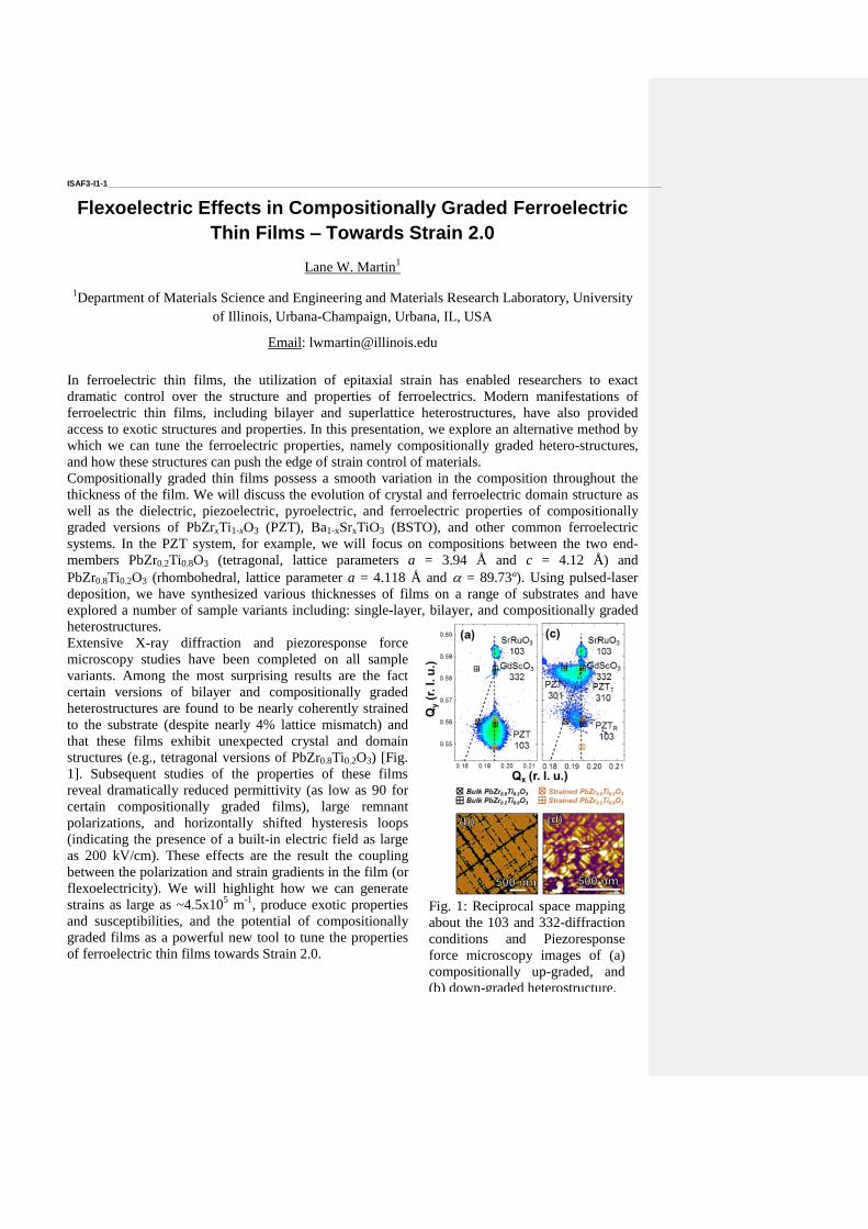
ISAF3-I1-1 ______________________________________________________________________________________________________________________
Flexoelectric Effects in Compositionally Graded Ferroelectric
Thin Films – Towards Strain 2.0
Lane W. Martin1
1Department of Materials Science and Engineering and Materials Research Laboratory, University
of Illinois, Urbana-Champaign, Urbana, IL, USA
Email: [email protected]
In ferroelectric thin films, the utilization of epitaxial strain has enabled researchers to exact
dramatic control over the structure and properties of ferroelectrics. Modern manifestations of
ferroelectric thin films, including bilayer and superlattice heterostructures, have also provided
access to exotic structures and properties. In this presentation, we explore an alternative method by
which we can tune the ferroelectric properties, namely compositionally graded hetero-structures,
and how these structures can push the edge of strain control of materials.
Compositionally graded thin films possess a smooth variation in the composition throughout the
thickness of the film. We will discuss the evolution of crystal and ferroelectric domain structure as
well as the dielectric, piezoelectric, pyroelectric, and ferroelectric properties of compositionally
graded versions of PbZrxTi1-xO3 (PZT), Ba1-xSrxTiO3 (BSTO), and other common ferroelectric
systems. In the PZT system, for example, we will focus on compositions between the two end-
members PbZr0.2Ti0.8O3 (tetragonal, lattice parameters a = 3.94 Å and c = 4.12 Å) and
PbZr0.8Ti0.2O3 (rhombohedral, lattice parameter a = 4.118 Å and = 89.73º). Using pulsed-laser
deposition, we have synthesized various thicknesses of films on a range of substrates and have
explored a number of sample variants including: single-layer, bilayer, and compositionally graded
heterostructures.
Extensive X-ray diffraction and piezoresponse force
microscopy studies have been completed on all sample
variants. Among the most surprising results are the fact
certain versions of bilayer and compositionally graded
heterostructures are found to be nearly coherently strained
to the substrate (despite nearly 4% lattice mismatch) and
that these films exhibit unexpected crystal and domain
structures (e.g., tetragonal versions of PbZr0.8Ti0.2O3) [Fig.
1]. Subsequent studies of the properties of these films
reveal dramatically reduced permittivity (as low as 90 for
certain compositionally graded films), large remnant
polarizations, and horizontally shifted hysteresis loops
(indicating the presence of a built-in electric field as large
as 200 kV/cm). These effects are the result the coupling
between the polarization and strain gradients in the film (or
flexoelectricity). We will highlight how we can generate
strains as large as ~4.5x10⁵ m
-1, produce exotic properties
and susceptibilities, and the potential of compositionally
graded films as a powerful new tool to tune the properties
of ferroelectric thin films towards Strain 2.0.
Fig. 1: Reciprocal space mapping
about the 103 and 332-diffraction
conditions and Piezoresponse
force microscopy images of (a)
compositionally up-graded, and
(b) down-graded heterostructure.

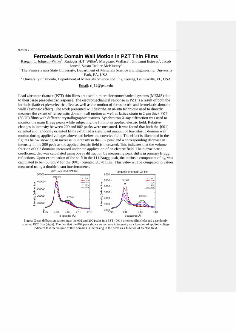
ISAF3-I1-2 ______________________________________________________________________________________________________________________
Ferroelastic Domain Wall Motion in PZT Thin Films Raegan L. Johnson-Wilke
1, Rudeger H.T. Wilke
1, Margeaux Wallace
1, Giovanni Esteves
2, Jacob
Jones2, Susan Trolier-McKinstry
1
1 The Pennsylvania State University, Department of Materials Science and Engineering, University
Park, PA, USA 2 University of Florida, Department of Materials Science and Engineering, Gainesville, FL, USA
Email: [email protected]
Lead zirconate titanate (PZT) thin films are used in microelectromechanical systems (MEMS) due
to their large piezoelectric response. The electromechanical response in PZT is a result of both the
intrinsic (lattice) piezoelectric effect as well as the motion of ferroelectric and ferroelastic domain
walls (extrinsic effect). The work presented will describe an in-situ technique used to directly
measure the extent of ferroelastic domain wall motion as well as lattice strain in 2 μm thick PZT
(30/70) films with different crystallographic textures. Synchrotron X-ray diffraction was used to
monitor the main Bragg peaks while subjecting the film to an applied electric field. Relative
changes in intensity between 200 and 002 peaks were measured. It was found that both the {001}
oriented and randomly oriented films exhibited a significant amount of ferroelastic domain wall
motion during applied voltages above and below the coercive field. The effect is illustrated in the
figures below showing an increase in intensity in the 002 peak and a corresponding decrease in
intensity in the 200 peak as the applied electric field is increased. This indicates that the volume
fraction of 002 domains increased under the application of an electric field. The piezoelectric
coefficient, d33, was calculated using X-ray diffraction by measuring peak shifts in primary Bragg
reflections. Upon examination of the shift in the 111 Bragg peak, the intrinsic component of d33 was
calculated to be ~50 pm/V for the {001} oriented 30/70 film. This value will be compared to values
measured using a double beam interferometer.
1.95 2.00 2.05 2.10 2.150
10000
20000
30000
40000
50000
PZT 002
Inte
nsity (
arb
. units)
d-spacing (Å)
0 V
10 V
20 V
30 V
40 V
PZT 200
{001} oriented PZT film
1.95 2.00 2.05 2.102000
3000
4000
5000
6000
7000
8000
PZT 002
PZT 200
Inte
nsity (
arb
. units)
d-spacing (Å)
0 V
34 V
51 V
68 V
85 V
Randomly oriented PZT film
Figure: X-ray diffraction pattern near the 002 and 200 peaks in a PZT {001} oriented film (left) and a randomly
oriented PZT film (right). The fact that the 002 peak shows an increase in intensity as a function of applied voltage
indicates that the volume of 002 domains is increasing in the films as a function of electric field.
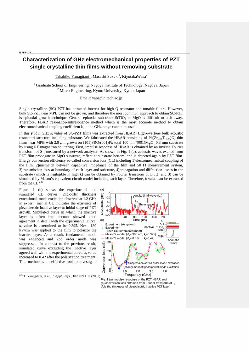
-100
-80
-60
-40
-20
0
Am
plit
ud
e (
dB
)
20016012080400Time (ns)
30
20
10
0
Co
nve
rsio
n lo
ss (
dB
)
4.03.02.01.00.0
Frequency (GHz)
Experiment (As grown) Experiment
(After 130 kV/cm treatment) Mason's model (dn= 300 nm, kt=0.395)
Mason's model (dn= 0 nm kt=0.42)
Suppression of 2nd order mode excitation
Enhancement of fundamental mode excitation
AuPZT
Inactive PZT: dnSRO
PtMgO
Acoustic wave
(a)
(b)
Longitudinal wave (L1)
LS1
Shear wave
Fig. 1 (a) Impulse response of the PZT HBAR and
(b) conversion loss obtained from Fourier transform of L1.
dn is the thickness of piezoelectric inactive PZT layer.
ISAF3-I1-3 ______________________________________________________________________________________________________________________
Characterization of GHz electromechanical properties of PZT
single crystalline thin films without removing substrate
Takahiko Yanagitani1, Masashi Suzuki
1, KiyotakaWasa
2
1 Graduate School of Engineering, Nagoya Institute of Technology, Nagoya, Japan
2 Micro-Engineering, Kyoto University, Kyoto, Japan
Email: [email protected]
Single crystalline (SC) PZT has attracted interest for high Q resonator and tunable filters. However,
bulk SC-PZT near MPB can not be grown, and therefore the most common approach to obtain SC-PZT
is epitaxial growth technique. General epitaxial substrate: SrTiO3 or MgO is difficult to etch away.
Therefore, FBAR resonance-antiresonance method which is the most accurate method to obtain
electromechanical coupling coefficient kt in the GHz range cannot be used.
In this study, GHz kt value of SC-PZT films was extracted from HBAR (High-overtone bulk acoustic
resonator) structure including substrate. We fabricated the HBAR consisting of Pb(Zr0.53Ti0.47)O3 thin
films near MPB with 2.8 m grown on (101)SRO/(001)Pt: total 100 nm /(001)MgO: 0.3 mm substrate
by using RF magnetron sputtering. First, impulse response of HBAR is obtained by an inverse Fourier
transform of S11 measured by a network analyzer. As shown in Fig. 1 (a), acoustic waves excited from
PZT film propagate in MgO substrate, reflect at substrate bottom, and is detected again by PZT film.
Energy conversion efficiency so-called conversion loss (CL) including 1)electromechanical coupling of
the film, 2)mismatch between capacitive impedance of the film and 50 measurement system,
3)transmission loss at boundary of each layer and substrate, 4)propagation and diffraction losses in the
substrate (which is negligible in high k) can be obtained by Fourier transform of L1. 2) and 3) can be
simulated by Mason’s equivalent circuit model including each layer. Therefore, k value can be extracted
from the CL 236
Figure 1 (b) shows the experimental and
simulated CL curves. 2nd-order thickness
extensional mode excitation observed at 1.2 GHz
in experi mental CL indicates the existence of
piezoelectric inactive layer at initial stage of PZT
growth. Simulated curve in which the inactive
layer is taken into account showed good
agreement in detail with the experimental curve.
kt value is determined to be 0.395. Next, 130
kV/cm was applied to the film to polarize the
inactive layer. As a result, fundamental mode
was enhanced and 2nd order mode was
suppressed. In contrast to the previous result,
simulated curve excluding the inactive layer
agreed well with the experimental curve. kt value
increased to 0.42 after the polarization treatment.
This method is an effective tool to investigate
236
T. Yanagitani, et al., J. Appl. Phys., 102, 024110, (2007).

polarization state and kt value in the single
crystalline PZT films.
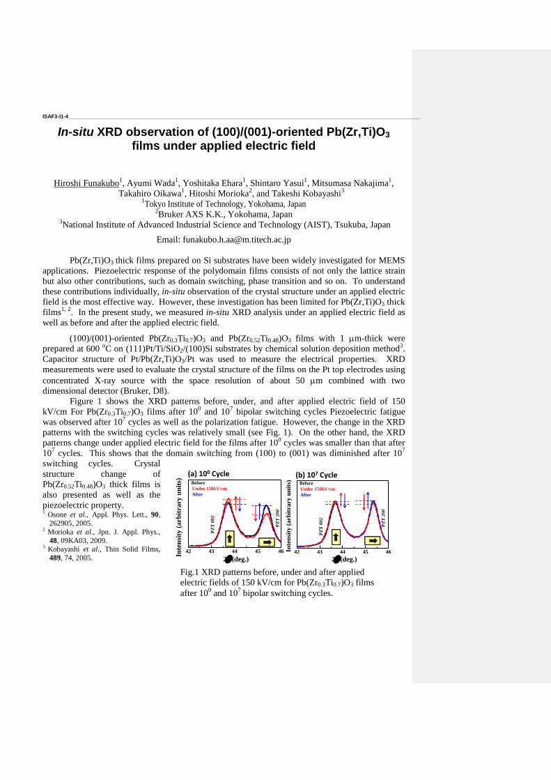
ISAF3-I1-4 ______________________________________________________________________________________________________________________
In-situ XRD observation of (100)/(001)-oriented Pb(Zr,Ti)O3 films under applied electric field
Hiroshi Funakubo1, Ayumi Wada
1, Yoshitaka Ehara
1, Shintaro Yasui
1, Mitsumasa Nakajima
1,
Takahiro Oikawa1, Hitoshi Morioka
2, and Takeshi Kobayashi
3
1Tokyo Institute of Technology, Yokohama, Japan
2Bruker AXS K.K., Yokohama, Japan
3National Institute of Advanced Industrial Science and Technology (AIST), Tsukuba, Japan
Email: [email protected]
Pb(Zr,Ti)O3 thick films prepared on Si substrates have been widely investigated for MEMS
applications. Piezoelectric response of the polydomain films consists of not only the lattice strain
but also other contributions, such as domain switching, phase transition and so on. To understand
these contributions individually, in-situ observation of the crystal structure under an applied electric
field is the most effective way. However, these investigation has been limited for Pb(Zr,Ti)O3 thick
films1, 2
. In the present study, we measured in-situ XRD analysis under an applied electric field as
well as before and after the applied electric field.
(100)/(001)-oriented Pb(Zr0.3Ti0.7)O3 and Pb(Zr0.52Ti0.48)O3 films with 1 m-thick were
prepared at 600 oC on (111)Pt/Ti/SiO2/(100)Si substrates by chemical solution deposition method
3.
Capacitor structure of Pt/Pb(Zr,Ti)O3/Pt was used to measure the electrical properties. XRD
measurements were used to evaluate the crystal structure of the films on the Pt top electrodes using
concentrated X-ray source with the space resolution of about 50 m combined with two
dimensional detector (Bruker, D8).
Figure 1 shows the XRD patterns before, under, and after applied electric field of 150
kV/cm For Pb(Zr0.3Ti0.7)O3 films after 100 and 10
7 bipolar switching cycles Piezoelectric fatigue
was observed after 107 cycles as well as the polarization fatigue. However, the change in the XRD
patterns with the switching cycles was relatively small (see Fig. 1). On the other hand, the XRD
patterns change under applied electric field for the films after 100 cycles was smaller than that after
107 cycles. This shows that the domain switching from (100) to (001) was diminished after 10
7
switching cycles. Crystal
structure change of
Pb(Zr0.52Ti0.48)O3 thick films is
also presented as well as the
piezoelectric property. 1
Osone et al., Appl. Phys. Lett., 90,
262905, 2005. 2
Morioka et al., Jpn. J. Appl. Phys.,
48, 09KA03, 2009. 3
Kobayashi et al., Thin Solid Films,
489, 74, 2005.
42 43 44 45 46
In
ten
sity
(a
rbit
rary
un
its)
2 (deg.)
PZ
T 0
02
PZ
T 2
00
Before
Under 150kV/cm
After
42 43 44 45 46
In
ten
sity
(arb
itra
ry u
nit
s)
2 (deg.)
PZ
T 0
02
PZ
T 2
00
(a) 100 Cycle (b) 107 CycleBefore
Under 150kV/cm
After
Fig.1 XRD patterns before, under and after applied
electric fields of 150 kV/cm for Pb(Zr0.3Ti0.7)O3 films
after 100 and 10
7 bipolar switching cycles.
ISAF3-I1-5 ______________________________________________________________________________________________________________________
Piezoelectric responses of epitaxial PZT film-based
membrane in d31 and d33 actuation mode
Minh Nguyen1,2,3, Matthijn Dekkers1,2, Dave Blank1, Guus Rijnders1
1Inorganic Materials Science (IMS), MESA+ Institute for Nanotechnology, University
of Twente, P.O. Box 217, 7500AE Enschede, The Netherlands 2SolMateS B.V., Drienerlolaan 5, Building 6, 7522NB Enschede, The Netherlands
3International Training Institute for Materials Science (ITIMS), Hanoi University of Science and
Technology, No. 1 Dai Co Viet road, Hanoi, Vietnam
Email: [email protected]
The magnitude of the d33 coefficient is 2.0 to 2.5 times higher than the d31 coefficient. Therefore, the
generated open-circuit voltage of a d33-mode device will be much higher (20 times or greater) than that of the
d31-mode generator of similar dimensions, resulting in a potentially higher energy conversion factor. Hence,
the d33-mode is the key to make the thin-film PZT device for power generation237.
In this report, d31 and d33 actuation mode micromechanical systems piezoelectric actuators and sensors
were fabricated and compared to investigate their displacements and quality factors. For d31-mode
membrane, an epitaxial Pb(Zr0.52Ti0.48)O3 (PZT) thin film was deposited on SrRuO3-buffered YSZ/Si
substrate; whereas, the deposition of the epitaxial PZT thin film was done on YSZ/Si substrate for d33-
mode membrane. All layers of PZT film (500 nm), SrRuO3 electrode (100 nm) and yttria-stabilized
zirconia (YSZ, 50 nm) buffered-layer were deposited using pulsed laser deposition (PLD). Diameter and
thickness of the membranes were 300-1000 µm and 10 µm, respectively.
The piezoelectric responses, including piezoelectric displacement and quality factor, were performed
using a laser Doppler vibrometer (LDV). The piezoelectric displacement and quality factor of the d31
and d33-mode were 22.4 nm/V and 102, and 10.2 nm/V and 128, respectively, with 500-µm in
membrane diameter. In this study, the center displacements of membranes were measured at an ac-
voltage of 3 V and 8 kHz frequency (off-resonance); while the quality factors were calculated from
resonance peaks which were measured at an ac-voltage of 1 V and in the frequency range from 0 to 2
237
Y. B. Jeon, R. Sood, J. -h. Jeong, S. -G. Kim, “MEMS power generator with transverse mode thin film PZT”, Sen. Actuators A, vol.
122, p. 16-22, 2005; W. J. Choi, Y. Jeon, J. H. Jeong, R. Sood, S. G. Kim, “Energy harvesting MEMS device based on thin film
piezoelectric cantilevers”, J. Electroceram., vol. 17, p. 543-548, 2006.
Fig. 67: Piezoelectric displacements of (a) d31-mode and (b) d33-mode membranes. The diameter
of membranes is 500 µm. All measurements are performed at an ac-voltage of 3 V and 8 kHz
frequency.

MHz. The effects of diameter membrane on the piezoelectric responses of the d31 and d33 mode have
been also investigated.

Piezoelectric Energy Harvesting
CLUB B
Wednesday, July 24 2013, 04:30 pm - 06:00 pm
Chair: Paula Vilarinho
Universoty of Aveiro
ISAF4-I2-1 ______________________________________________________________________________________________________________________
Energy Harvesting with Piezoelectric MEMS
Paul Muralt, Andrea Mazzalai, Ramin Matloub
Ceramics Laboratory, EPFL, Lausanne, Switzerland
Email: [email protected]
During recent years, energy harvesting from vibration and motion sources has attracted much
interest. Electrical power generators based on piezoelectric materials were investigated, first as
flexible piezoelectric bulk composite materials containing PZT ceramics, and later also as MEMS
devices based on thin films, or even nanowires. In case of micro power devices, the main target
applications are wireless communication, sensors, and specifically wireless sensors. Average supply
powers of 100 µW are sufficient to operate wireless nodes with low duty cycles. There is general
agreement on the fact that motions and vibrations constitute the most versatile and ubiquitous
ambient energy sources available, if light harvesting is excluded by the application. The progress in
piezoelectric thin films and MEMS technology has lead to the development of demonstration
devices that show sufficiently large power outputs and voltage levels, i.e. more than several 100
µW/cm2 at over one volt. The standard configuration is to use parallel plate capacitor geometry
exploiting the transverse piezoelectric coefficient. It looks evident that Pb(ZrTi)O3 and related
ferroelectric materials should be the best choice. However, ferroelectric thin films exhibit high
dielectric constants – meaning low voltage output - and usually suffer from limited remanent
polarization. Remedies can be found in using interdigitated electrode systems, or imprinted films.
Another solution, however, could be to use AlScN thin films. Substituting Al in part by Sc leads to
higher e31,f coefficients with only a moderate increase of the dielectric constant.
In this talk, the principles of piezoelectric energy harvesting will be introduced and illustrated with
achieved results. Direct strain coupling to moving parts is compared to acceleration coupling by
means of inertial masses. Specific thin films issues will be addressed such as material’s choice, and
electrode configurations. The interdigitated electrode system will be discussed in more detail,
including growth on insulators, poling, domain issues and performance. The energy figure of merit
e*h as derived from measurements is introduced to compare materials and electrode systems.
Experimental results will be compared to numerical simulations.
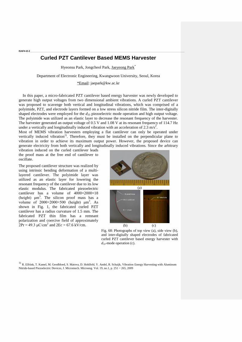
ISAF4-I2-2 ______________________________________________________________________________________________________________________
Curled PZT Cantilever Based MEMS Harvester
Hyeonsu Park, Jongcheol Park, Jaeyeong Park*
Department of Electronic Engineering, Kwangwoon University, Seoul, Korea
*Email: [email protected]
In this paper, a micro-fabricated PZT cantilever based energy harvester was newly developed to
generate high output voltages from two dimensional ambient vibrations. A curled PZT cantilever
was proposed to scavenge both vertical and longitudinal vibrations, which was comprised of a
polyimide, PZT, and electrode layers formed on a low stress silicon nitride film. The inter-digitally
shaped electrodes were employed for the d33 piezoelectric mode operation and high output voltage.
The polyimide was utilized as an elastic layer to decrease the resonant frequency of the harvester.
The harvester generated an output voltage of 0.5 V and 1.08 V at its resonant frequency of 114.7 Hz
under a vertically and longitudinally induced vibration with an acceleration of 2.3 m/s2.
Most of MEMS vibration harvesters employing a flat cantilever can only be operated under
vertically induced vibration1)
. Therefore, they must be installed on the perpendicular plane to
vibration in order to achieve its maximum output power. However, the proposed device can
generate electricity from both vertically and longitudinally induced vibrations. Since the arbitrary
vibration induced on the curled cantilever leads
the proof mass at the free end of cantilever to
oscillate.
The proposed cantilever structure was realized by
using intrinsic bending deformation of a multi-
layered cantilever. The polyimide layer was
utilized as an elastic layer for lowering the
resonant frequency of the cantilever due to its low
elastic modulus. The fabricated piezoelectric
cantilever has a volume of 4000×2000×18
(height) μm3. The silicon proof mass has a
volume of 2000×2000×500 (height) μm3. As
shown in Fig. 1, the fabricated curled PZT
cantilever has a radius curvature of 1.5 mm. The
fabricated PZT thin film has a remnant
polarization and coercive field of approximately
2Pr = 49.3 μC/cm2 and 2Ec = 67.6 kV/cm.
1) R. Elfrink, T. Kamel, M. Geodbloed, S. Matova, D. Hohlfeld, Y. Andel, R. Schaijk, Vibration Energy Harvesting with Aluminum
Nitride-based Piezoelectric Devices, J. Micromech. Microeng. Vol. 19, no.1, p. 251 ~ 265, 2009
(a)
(b) (c)
Fig. 68: Photographs of top view (a), side view (b),
and inter-digitally shaped electrodes of fabricated
curled PZT cantilever based energy harvester with
d33-mode operation (c).

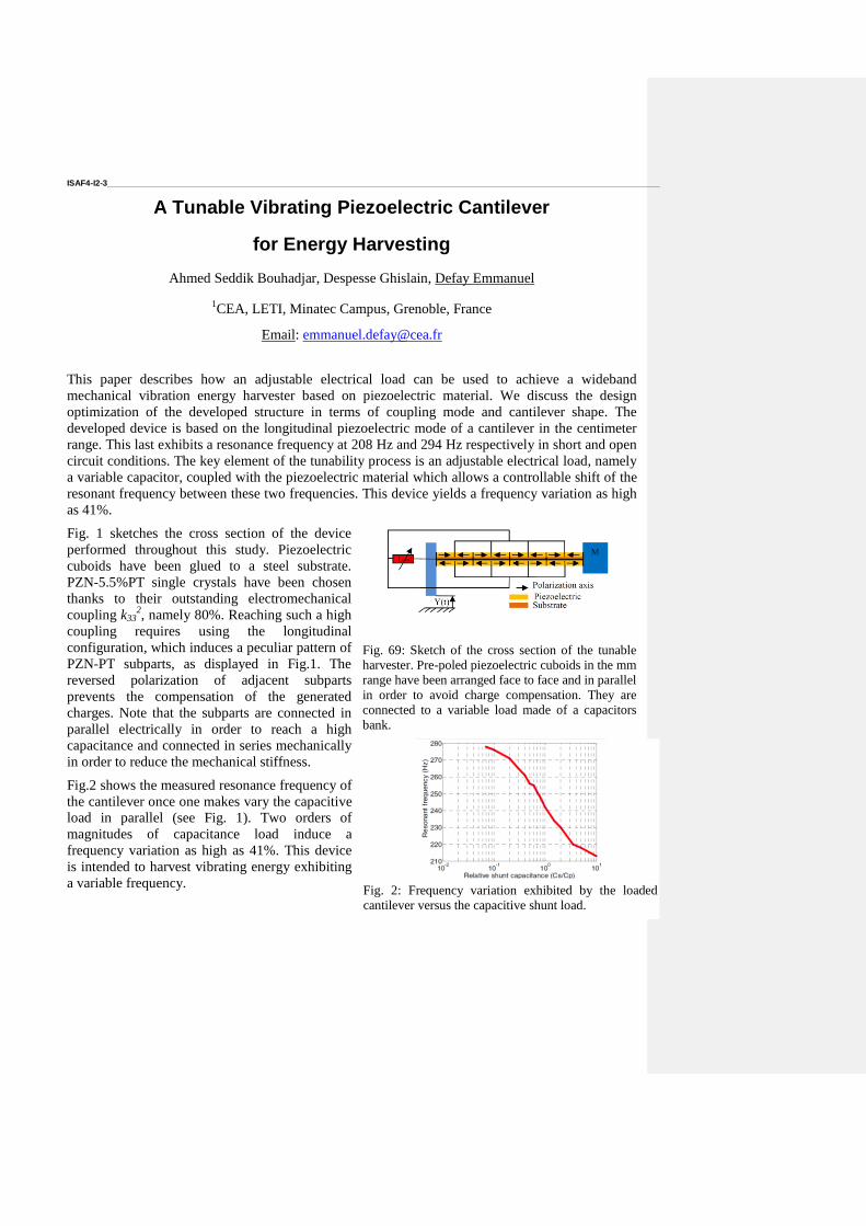
ISAF4-I2-3 ______________________________________________________________________________________________________________________
A Tunable Vibrating Piezoelectric Cantilever
for Energy Harvesting
Ahmed Seddik Bouhadjar, Despesse Ghislain, Defay Emmanuel
1CEA, LETI, Minatec Campus, Grenoble, France
Email: [email protected]
This paper describes how an adjustable electrical load can be used to achieve a wideband
mechanical vibration energy harvester based on piezoelectric material. We discuss the design
optimization of the developed structure in terms of coupling mode and cantilever shape. The
developed device is based on the longitudinal piezoelectric mode of a cantilever in the centimeter
range. This last exhibits a resonance frequency at 208 Hz and 294 Hz respectively in short and open
circuit conditions. The key element of the tunability process is an adjustable electrical load, namely
a variable capacitor, coupled with the piezoelectric material which allows a controllable shift of the
resonant frequency between these two frequencies. This device yields a frequency variation as high
as 41%.
Fig. 1 sketches the cross section of the device
performed throughout this study. Piezoelectric
cuboids have been glued to a steel substrate.
PZN-5.5%PT single crystals have been chosen
thanks to their outstanding electromechanical
coupling k332, namely 80%. Reaching such a high
coupling requires using the longitudinal
configuration, which induces a peculiar pattern of
PZN-PT subparts, as displayed in Fig.1. The
reversed polarization of adjacent subparts
prevents the compensation of the generated
charges. Note that the subparts are connected in
parallel electrically in order to reach a high
capacitance and connected in series mechanically
in order to reduce the mechanical stiffness.
Fig.2 shows the measured resonance frequency of
the cantilever once one makes vary the capacitive
load in parallel (see Fig. 1). Two orders of
magnitudes of capacitance load induce a
frequency variation as high as 41%. This device
is intended to harvest vibrating energy exhibiting
a variable frequency.
Fig. 69: Sketch of the cross section of the tunable
harvester. Pre-poled piezoelectric cuboids in the mm
range have been arranged face to face and in parallel
in order to avoid charge compensation. They are
connected to a variable load made of a capacitors
bank.
Fig. 2: Frequency variation exhibited by the loaded
cantilever versus the capacitive shunt load.

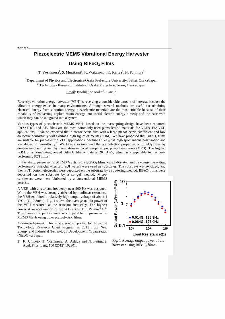
ISAF4-I2-4 ______________________________________________________________________________________________________________________
Piezoelectric MEMS Vibrational Energy Harvester
Using BiFeO3 Films
T. Yoshimura1, S. Murakami
2, K. Wakazono
1, K. Kariya
1, N. Fujimura
1
1Department of Physics and Electronics/Osaka Prefecture University, Sakai, Osaka/Japan
2 Technology Research Institute of Osaka Prefecture, Izumi, Osaka/Japan
Email: [email protected]
Recently, vibration energy harvester (VEH) is receiving a considerable amount of interest, because the
vibration energy exists in many environments. Although several methods are useful for obtaining
electrical energy from vibration energy, piezoelectric materials are the most suitable because of their
capability of converting applied strain energy into useful electric energy directly and the ease with
which they can be integrated into a system.
Various types of piezoelectric MEMS VEHs based on the mass-spring design have been reported.
Pb(Zr,Ti)O3 and AlN films are the most commonly used piezoelectric materials for VEHs. For VEH
applications, it can be expected that a piezoelectric film with a large piezoelectric coefficient and low
dielectric permittivity will exhibit a high figure of merits (FOM). We have proposed that BiFeO3 films
are suitable for piezoelectric VEH applications, because BiFeO3 has high spontaneous polarization and
low dielectric permittivity.1) We have also improved the piezoelectric properties of BiFeO3 films by
domain engineering and by using strain-induced morphotropic phase boundaries (MPB). The highest
FOM of a domain-engineered BiFeO3 film to date is 20.8 GPa, which is comparable to the best-
performing PZT films.
In this study, piezoelectric MEMS VEHs using BiFeO3 films were fabricated and its energy harvesting
performance was characterized. SOI wafers were used as substrates. The substrate was oxidized, and
then Pt/Ti bottom electrodes were deposited on the substrate by a sputtering method. BiFeO3 films were
deposited on the substrate by a sol-gel method. Micro-
cantilevers were then fabricated by a conventional MEMS
process.
A VEH with a resonant frequency near 200 Hz was designed.
While the VEH was strongly affected by nonlinear resonance,
the VEH exhibited a relatively high output voltage of about 1
V·G-1 (G: 9.8m/s2). Fig. 1 shows the average output power of
the VEH measured at the resonant frequency. The highest
power at an acceleration of 0.014 Grms is 3.3 W·mm-3·G-2.
This harvesting performance is comparable to piezoelectric
MEMS VEHs using other piezoelectric films.
Acknowledgement: This study was supported by Industrial
Technology Research Grant Program in 2011 from New
Energy and Industrial Technology Development Organization
(NEDO) of Japan.
1) K. Ujimoto, T. Yoshimura, A. Ashida and N. Fujimura,
Appl. Phys. Lett., 100 (2012) 102901.
Load Resistance()
Ou
tpu
t P
ow
er
(W
·mm
-3·G
-2) 10
0.1105 106 107
1
0.014G, 195.3Hz
0.084G, 196.0Hz
Fig. 1 Average output power of the
harvester using BiFeO3 films.

ISAF4-I2-5 ______________________________________________________________________________________________________________________
Efficient flexible nanogenerator made of organic ferroelectric
dabcoHReO4
Dmitry Isakov1, Etelvina de Matos Gomes
1, Bernardo Almeida
1, Igor Bdikin
2 and Andrei Kholkin
3.
1 University of Minho, Center of Physics, Campus de Gualtar, 4710-059 Braga, Portugal
2 University of Aveiro, Department of Mechanical Engineering and TEMA, 3810-193 Aveiro,
Portugal 3Department of Ceramics and Glass Engineering & Center for Research in Ceramic and Composite
Materias (CICECO), University of Aveiro, 3810-193 Aveiro, Portugal
Email: [email protected]
In the last years, one-dimensional nanostructures have gathered significant scientific, technological
and industrial interest, for application in fields such as drug delivery and regenerative medicine,
sensing and chemical catalysis, nanophotonics and nanoelectronics. In this regard special attention
has been paid to organic materials due to their low cost and structural flexibility. However, while
organic 1D nanostructures can be produced by a variety of laboratory methods (polymerization
against porous templates, self-assembly, soft lithographies etc.), electrospinning is one of the few
technologies which can be adequately scaled-up to an industrial level. The electrospinning process
is based on the uniaxial elongation of a jet, ejected from the surface of a charged polymer solution
possessing sufficient molecular entanglements, in the presence of an intense electric field. The
plastic stretching of the electrified jet and concomitant solvent evaporation results in the formation
of continuous nanofibers with significant cross-section reduction of up to six orders of magnitude.
The important feature of electrospun nanofibers is that the strong shear and electrostatic forces
experienced during the process cause the alignment of dopants, molecules and chains within the
principal fiber axis. This is an especially attractive phenomenon for polar materials, since
promoting such internal molecular orientation (self-assembling) of the organic molecules can also
result in achieving polarized emission or enhanced polar properties and an anisotropic alignment of
active components is expected to bring in new features and applications. Recent interest on
electrospun nanofibers for piezoelectric applications reveals a big potential of this low-cost
nanomanufacturing process for the development of fiber-based energy harvesting elements.
However, up to date, among the various organic polar materials, only nanofibers of PVDF have
been used in piezoelectric actuators. In this work, we present a production of nanofibers of a room
temperature hybrid organic-inorganic ferroelectric 1,4-diazabicyclo[2.2.2]-octane perrhenate
(dabcoHReO4).
The nanofibers have preferentially oriented dabcoHReO4 nanocrystals with their polarized
hydrogen bonds along the fiber axis displaying enhanced piezoelectricity and second harmonic
generation response. An efficient strain-electricity flexible nanogenerator based on parallel array
dabcoHReO4 nanofibers reveal above 100 mV output voltage and can be used as a sensitive
biocompatible strain sensor and implantable voltage generator.

Bulk Piezoelectric Materials
CLUB C
Wednesday, July 24 2013, 04:30 pm - 05:45 pm
Chair: Pavel Mokry
Technical University of Liberec
ISAF4-I3-1 ______________________________________________________________________________________________________________________
Ian Reaney1
1Materials Science and Engineering, Unversity of Sheffield, Sheffield, South Yorkshire, United Kingdom
From Materials Discovery to Prototype Devices
Ian M. Reaney
Functional Materials Group
Materials Science and Engineering
University of Sheffield, UK
The main goals of the Functional Materials Group (FMG) at Sheffield are to develop new materials,
characterise their structure and functional properties and develop prototype devices to demonstrate
their commercial potential. The remit of the FMG is broad with a wide range of projects that focus
on ionic conduction for Li-battery applications, magnetic memories and sensors, piezoelectrics,
MW and rf dielectrics and thermoelectrics. This presentation will review recent advances at
Sheffield in the development of i) Pb-niobate thins films for tunable filters, ii) high TC piezoelectric
ceramics and iii) dielectrically loaded MW antennas An overview of the key driving forces in the
science and technology of these topics will be presented followed by detailed descriptions of the
key advances made.
ISAF4-I3-2 ______________________________________________________________________________________________________________________
Phase Transition Toughening in Antiferroelectric Ceramics
Xiaoli Tan1, S. Eli Young
1, Yohan Seo
2, Kyle G. Webber,
2 Jürgen Rödel
2
1Department of Materials Science and Engineering, Iowa State University, Ames, Iowa/USA
2Institute of Materials Science, Technische Universität Darmstadt, Darmstadt/ Germany
Email: [email protected]
In antiferroelectric solid crystals, the antiparallel electrical dipoles are originated from cation
displacements in the unit cell. Aligning these originally antiparallel electric dipoles to the direction
of the applied electric field requires cooperative adjustment of the crystal lattice in many unit cells
and corresponds to a first order displacive phase transition. The vast majority of antiferroelectric
ceramics are based on the prototype compound PbZrO3 with the perovskite structure. In these
oxides, the antiferroelectric-to-ferroelectric phase transition manifests itself in the development of a
large polarization and is generally accompanied by a significant volume expansion when the
applied field exceeds a critical magnitude EF. The developed macroscopic polarization results from
the antiparallel dipoles being forced parallel at the transition. The associated volume expansion at
the phase transition implies that there might be a toughening effect.
In this study, a series of Pb0.99Nb0.02[(Zr0.57Sn0.43)1-yTiy]0.98O3 (PNZST43/100y/2) solid solution
ceramics were investigated for their antiferroelectric ferroelectric phase transitions. It was found
that the induced ferroelectric phase is metastable in compositions with 0.07 ≤ y ≤ 0.08 at room
temperature. Strain measurements and X-ray diffraction analysis confirmed that the ferroelectric
phase has a larger volume than the antiferroelectric phase. Crack growth resistance tests were
carried out at room temperature on compact tension specimens with dimensions of 24 mm 25 mm
3 mm in PNZST43/6.1/2, 43/6.4/2, 43/6.7/2, 43/8/2, 43/10/2 ceramics. The results indicate the
fracture toughness in PNZST43/8/2 is much higher than other compositions, verifying the
antiferroelectric-to-ferroelectric phase transition toughening effect. The localized phase transition
zone was directly mapped with microRaman spectroscopy.
ISAF4-I3-3 ______________________________________________________________________________________________________________________
High Power Piezoelectric Properties of
Some Bismuth Layer-Structured Ferroelectric Ceramics and
their Applications to Ultrasonic Motors
Hajime Nagata1, Shun Endo
1, Tadashi Takenaka
1
1Department of Electrical Engineering, Faculty of Science and Technology,
Tokyo University of Science/Japan
Email: [email protected]
Recently, many high-power piezoelectric ceramic devices, such as ultrasonic motors and
piezoelectric transducers, have been developed so far. Hard Pb(Zr,Ti)O3 (PZT) ceramics with a high
piezoelectric strain constant dij and a high mechanical quality factor Qm are often used in high-
power piezoelectric applications. Normally, hard PZT-based ceramics are driven at a vibration
velocity of 1 m/s owing to a resonance frequency change, heat generation and Qm reduction.
Additionally, PZT ceramics contain a large amount of PbO. Therefore, lead-free piezoelectric
materials for replacing PZT have recently been demanded from the viewpoint of environmental
protection. The family of bismuth layer structured ferroelectrics (BLSFs) has been attracting
attention as a lead-free piezoelectric material for resonators and filters because they have large Qm
values. Thus, they seem to be good candidates for high-power ceramic devices realizing a large-
amplitude and a linear stability against vibration velocity238,239
. So, in this study, high-power
piezoelectric characteristics under continuous driving were studied on some bismuth layer-
structured ferroelectric ceramics, i.e., Sr0.25Bi2.75Ti0.75Ta1.25O9 (SBTT, m=2), Bi4Ti2.98V0.02O12
(BITV, m=3), Bi4Ti3O12-SrBi4Ti4O15 + MnCO3 0.2 wt% (BIT-SBTi, m=3, 4), and
(Sr0.7Ca0.3)2Bi4Ti5O18 + MnCO3 0.2 wt% (SCBT, m=5).
The vibration velocities, v0-p, of SBTT, BIT-SBTi, and SCBT ceramics were above 2.0 m/s at 5
V/mm. Also, we observed that the resonance frequency changes and temperatures on the sample
surfaces for SBTT, BIT-SBTi, and SCBT ceramics were less than 1.0% and 50 ºC at a v0-p of 2.0
m/s, respectively. The high-power characteristics of the ceramics were superior to those of BITV
and hard PZT at a vibration velocity v0-p > 0.6 m/s. Therefore, SBTT, BIT-SBTi and SCBT
ceramics are promising candidates for lead-free high-power applications requiring high vibration
velocity and frequency stability.
As an example of the high-power piezoelectric application, we tried to demonstrate an ultrasonic
motor using some BLSF ceramics. The ultrasonic motor we fabricated by some BLSF ceramics
successfully rotated under the large amplitude driving around the resonance frequency. The
maximum rotation-speed was over 600 rpm on the ultrasonic motor fabricated by BIT-SBTi, and
SCBT ceramics. This rotation-speed was much higher than that in the motors by hard PZT
ceramics. Additionally, the resonance frequency of BLSF motor was almost constant under the
large amplitude driving. In fact, the ultrasonic motor by SCBT ceramic was continuously rotated for
more than 5 min without any control of the resonance frequency. This means that the ultrasonic
238
S. Kawada, H. Ogawa, M. Kimura, K. Shiratsuyu, and H. Niimi: Jpn. J. Appl. Phys. ,45 (2006) 7455. 239
H. Ogawa, S. Kawada, M. Kimura, K. Shiratsuyu, and Y. Sakabe: IEEE Trans. UFFC, 54 (2007) 2500.

motor using BLSF ceramics can eliminate the additional circuit for pursuing the resonance
frequency.
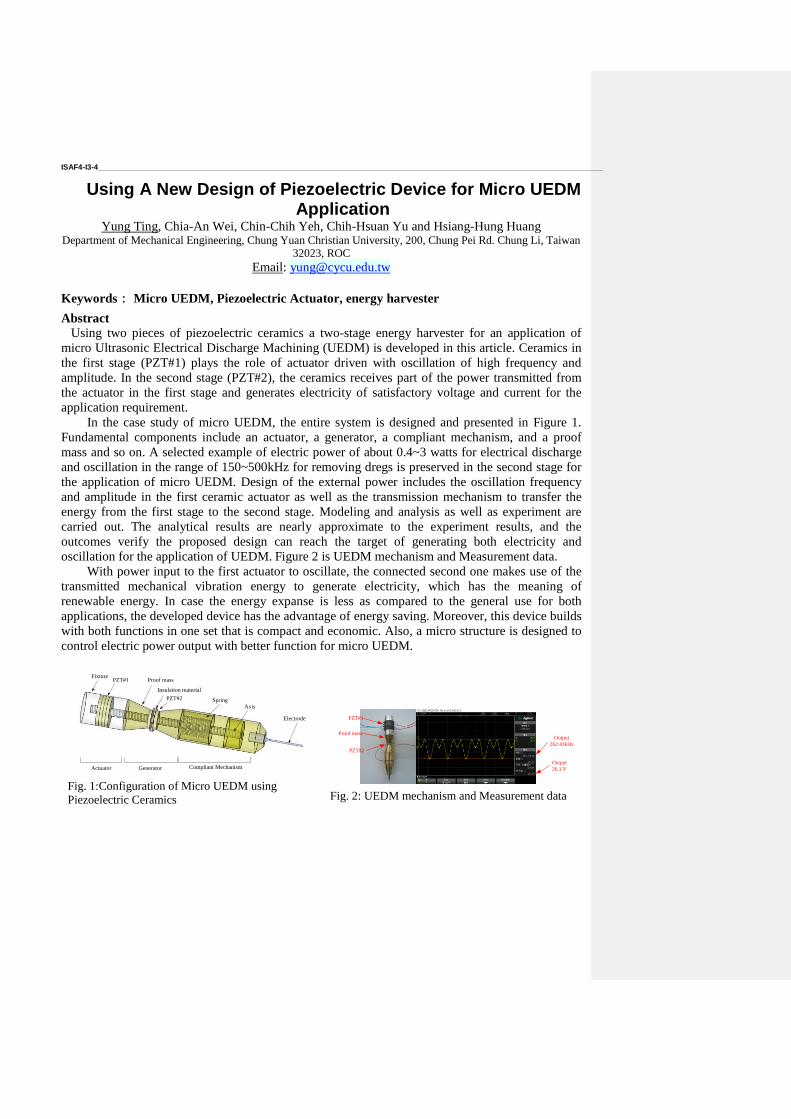
ISAF4-I3-4 ______________________________________________________________________________________________________________________
Using A New Design of Piezoelectric Device for Micro UEDM Application
Yung Ting, Chia-An Wei, Chin-Chih Yeh, Chih-Hsuan Yu and Hsiang-Hung Huang
Department of Mechanical Engineering, Chung Yuan Christian University, 200, Chung Pei Rd. Chung Li, Taiwan
32023, ROC Email: [email protected]
Keywords: Micro UEDM, Piezoelectric Actuator, energy harvester
Abstract
Using two pieces of piezoelectric ceramics a two-stage energy harvester for an application of
micro Ultrasonic Electrical Discharge Machining (UEDM) is developed in this article. Ceramics in
the first stage (PZT#1) plays the role of actuator driven with oscillation of high frequency and
amplitude. In the second stage (PZT#2), the ceramics receives part of the power transmitted from
the actuator in the first stage and generates electricity of satisfactory voltage and current for the
application requirement.
In the case study of micro UEDM, the entire system is designed and presented in Figure 1.
Fundamental components include an actuator, a generator, a compliant mechanism, and a proof
mass and so on. A selected example of electric power of about 0.4~3 watts for electrical discharge
and oscillation in the range of 150~500kHz for removing dregs is preserved in the second stage for
the application of micro UEDM. Design of the external power includes the oscillation frequency
and amplitude in the first ceramic actuator as well as the transmission mechanism to transfer the
energy from the first stage to the second stage. Modeling and analysis as well as experiment are
carried out. The analytical results are nearly approximate to the experiment results, and the
outcomes verify the proposed design can reach the target of generating both electricity and
oscillation for the application of UEDM. Figure 2 is UEDM mechanism and Measurement data.
With power input to the first actuator to oscillate, the connected second one makes use of the
transmitted mechanical vibration energy to generate electricity, which has the meaning of
renewable energy. In case the energy expanse is less as compared to the general use for both
applications, the developed device has the advantage of energy saving. Moreover, this device builds
with both functions in one set that is compact and economic. Also, a micro structure is designed to
control electric power output with better function for micro UEDM.
Spring
PZT#1
PZT#2
Insulation material
Proof mass
Electrode
Fixture
Axis
Actuator Generator Compliant Mechanism
Fig. 1:Configuration of Micro UEDM using
Piezoelectric Ceramics
Output
262.43kHz
Output
26.1 V
PZT#2
PZT#1
Proof mass
Fig. 2: UEDM mechanism and Measurement data
ISAF4-I3-5 ______________________________________________________________________________________________________________________
Efficient Compensation of Nonlinear Transfer
Characteristics for Piezoceramic Actuators
Felix Wolf1, Hartmut Hirsch
1, Alexander Sutor
1, Stefan J. Rupitsch
1, Reinhard Lerch
1
1Chair of Sensor Technology, Friedrich-Alexander-University, Erlangen, Germany
Email: [email protected]
The hysteretic, nonlinear transfer characteristics is one of the main drawbacks when using
piezoceramic materials in actuator applications. Multiple effects on various length scales contribute
to this difficult material behavior, making precise positioning and manipulation tasks erroneous.
Two solutions are commonly used to overcome these tracking errors:
1. The use of amplifiers with charge output
2. Open- and closed-loop control strategies
The second solution is more favorable, since the
charge-strain relation is only linear in a limited
operational range and circuitry of charge
amplifiers has some disadvantages. However,
efficient models describing the nonlinear material
behavior are necessary for control strategies. The
Preisach hysteresis operator is such an efficient
model, but it allows only for the calculation of
the transfer characteristics in forward direction,
i.e.,
u(t) → fsim(t). An analytic inversion of this model
for calculating the input uinv(t) required for a
given output ftarget(t) does not exist.
In our previous work, we proposed a generalized Preisach model with an analytic weight function.
The model was extended to cover the influence of additional mechanical stress240
on the transfer
characteristics as well as of creep effects utilizing an additional creep operator241
.
The scope of the present contribution is to introduce a novel algorithm allowing for an efficient
iterative inversion of the Preisach operator. The algorithm is based on a sophisticated two-step
search procedure in the Preisach plane representing the “memory” of the material. The computing
time depends on the discretization M of the Preisach plane. As our investigations reveal, a
discretization level of M=200 is sufficient for precise inversion and prediction results (see Fig.1).
For this discretization level, a maximum sampling frequency of 3.45 kHz is allowed for the signals
to be inverted.
240
F. Wolf, A. Sutor, S. J. Rupitsch and R. Lerch, A generalized Preisach approach for piezoceramic materials
incorporating uniaxial compressive stress, J. Sen. Act. A, 2012, 186, 223-229 241
F. Wolf, A. Sutor, S. J. Rupitsch and R. Lerch, Modeling and measurement of creep- and rate-dependent hysteresis
in ferroelectric actuators, J. Sen. Act. A, 2011, 172, 245-252
Fig. 70: Desired target quantity ftarget, inverted
input-signal uinv(ftarget) for discretization level M =
200 as well as simulated model output fsim(uinv).

The model inversion is further verified via open-loop control of the strain output of soft PZT bulk
ceramics as well as of trimorph bending actuators. The model inversion we introduce shows to be
an efficient tool for compensating the nonlinearities in piezoceramic actuator applications.

ISAF Group 3 Posters
Forum Hall
Wednesday, July 24 2013, 01:00 pm - 04:30 pm
ISAF-P3C-1 _____________________________________________________________________________________________________________________
Properties of Hafnium/Zirconium doped (Na1/2Bi1/2TiO3) Relaxor-Ferroelectric
Ceramics Under Bias Electrical Field
DERYA KIRSEVER1 and HUSEYIN YILMAZ
2
1 Sakarya University, Department of Metallurgical and Materials Engineering, TURKEY
2 Gebze Institute of Technology, Department of Material Science and Engineering, TURKEY
[email protected], [email protected]
Abstract Lead-free piezoelectric materials are intensely studied due to being environmentally
friendly. Among them, sodium bismuth titanate (Na1/2Bi1/2TiO3, or NBT) and its various solid
solutions have been drawing special attention as a new candidate for their lead based counterparts.
There is a great demand for reducing the adverse effect of lead. In this study, Hafnium or Zirconium
doped grain oriented (Na1/2Bi1/2)TiO3 (NBT) ceramics with <001> orientation were fabricated by
Templated Grain Growth (TGG) method using anisotropically shaped SrTiO3 template particles.
These molten salt synthesized SrTiO3 platelets were tape cast with calcined NBT powder, and
sintered at 12000C for 6 h. Texture fractions up to 70% have been obtained. Hf
4 or Zr
4 doped
NBT ceramics were characterized by using X-Ray diffraction (XRD), scanning electron microscopy
(SEM), polarization and electromechanical measurements. Electromechanical properties of Hf+4
and
Zr+4
doped NBT ceramics were studied under electrical bias. Unipolar strains up to > 0.25% was
measured. Electrostrictive coefficient of Hf+4
doped NBT ceramics were determined to be 0.032
m4/C
2, which is much larger than that of PMN-based electrostrictive materials.

ISAF-P3C-2 _____________________________________________________________________________________________________________________
Simulation of the Locally Measured d33 of
Piezoelectric 1-3-Composites
Christoph Pientschke1, Sabine Kern
1, Hartmut S. Leipner
1
1Martin-Luther-University, Interdisciplinary Center of Materials Science (CMAT),
06099 Halle (Saale), Germany
Email: [email protected]
Piezoelectric 1-3-composites consist of aligned piezoelectric fibers or rods that are surrounded by a
polymer matrix. The effective piezoelectric coefficient d33,eff of the composite can be calculated
with analytic approximation formulas. The inputs of these formulas are the piezoelectric coefficient
d33 of the piezoelectric fibers or rods, their volume content and some mechanical properties of the
constituents. These formulas presume among others an uniform displacement of the composite
surface. However, the displacement of the surface is nonuniform. In addition to that the
displacement is measured with a local method that is sensitive to a certain area of the surface. So
the questions arises: How does the measurement process influence the measured mean d33 of the
composites and to what amount does it deviate from the prediction of the approximation formulas?
To answer these questions, the experimental situation was simulated using the finite-element-
method (FEM) and a subsequent analysis.
In the simulated experiment, the d33 is quasi-statically measured. For this purpose, the local
displacement is translated to a capacitive distance detector using a tappet touching the sample
surface within a measuring spot. The tappet is moved by the largest displacement within that spot.
The d33,eff of the 1-3-composites is determined by averaging the local measured piezoelectric
coefficients of several tappet positions. For the simulations, the local displacements of 1-3-
composites were calculated with FEM. 1-3-composites with periodically and randomly arranged
piezoelectric rods were investigated. The resulting data were displayed as a contour plot with pixel
values related to the local displacement. The measuring spot was represented by a circle. It was
randomly placed on the contour plot. The largest pixel value within that circle was regarded as
representation of the measured local d33. This procedures were repeated several hundred times. The
resulting values were statistically analyzed.
According to the simulations, the measured mean d33 and the effective d33,eff calculated by the
approximation formulas differ significantly. This deviation is not only affected by the measuring
spot diameter but also by the volume content of the piezoelectric rods and the thickness of the
composite. The approximation formulas overestimate the actual mean d33 of the composites. The
difference of the calculated d33,eff and the measured mean d33 is smaller than this because increasing
spot diameters result in an increase in the measured mean d33. In addition to that the distribution of
the measured d33 changes significantly with increasing spot diameters. For small spot diameters, the
distribution of the measured mean d33 and the actual value of the whole surface are similar. The
inner structure of the 1-3-composites influences the distribution of the measured d33. The standard
deviation of the measured d33 is a function of the spot diameter. It decreases with increasing spot
diameters. For small volume contents, it reaches a maximum before decreasing.
Summarizing, the simulations provide a new access to the understanding of the distribution of
locally measured d33 of piezoelectric 1-3-composites and to its relation to approximation formulas.

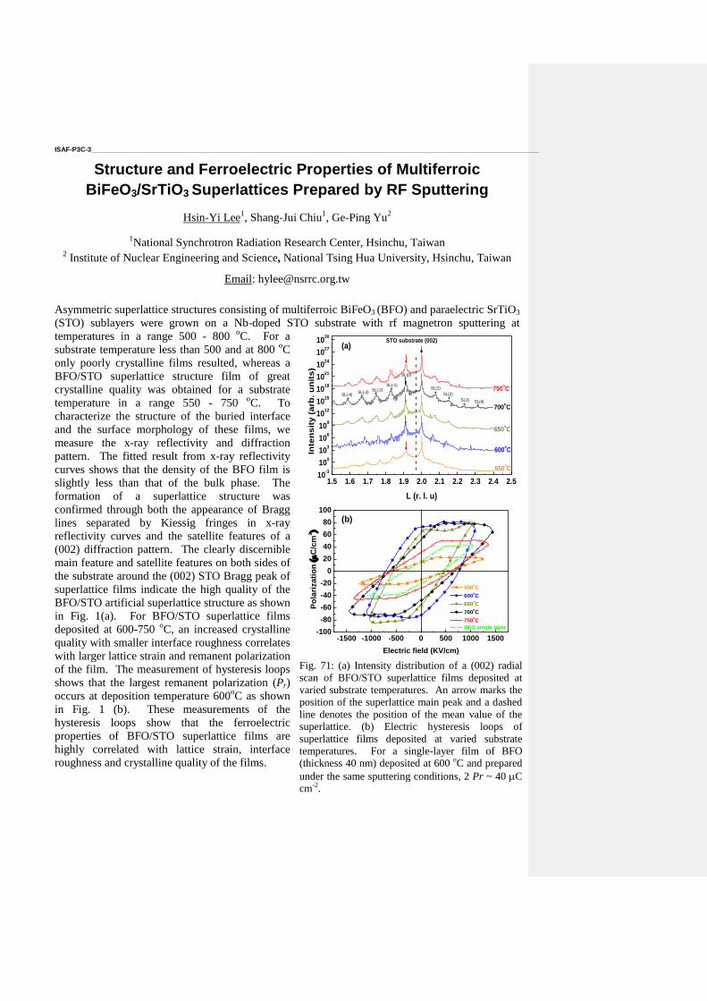
ISAF-P3C-3 _____________________________________________________________________________________________________________________
Structure and Ferroelectric Properties of Multiferroic
BiFeO3/SrTiO3 Superlattices Prepared by RF Sputtering
Hsin-Yi Lee1, Shang-Jui Chiu
1, Ge-Ping Yu
2
1National Synchrotron Radiation Research Center, Hsinchu, Taiwan
2 Institute of Nuclear Engineering and Science, National Tsing Hua University, Hsinchu, Taiwan
Email: [email protected]
Asymmetric superlattice structures consisting of multiferroic BiFeO3 (BFO) and paraelectric SrTiO3
(STO) sublayers were grown on a Nb-doped STO substrate with rf magnetron sputtering at
temperatures in a range 500 - 800 oC. For a
substrate temperature less than 500 and at 800 oC
only poorly crystalline films resulted, whereas a
BFO/STO superlattice structure film of great
crystalline quality was obtained for a substrate
temperature in a range 550 - 750 oC. To
characterize the structure of the buried interface
and the surface morphology of these films, we
measure the x-ray reflectivity and diffraction
pattern. The fitted result from x-ray reflectivity
curves shows that the density of the BFO film is
slightly less than that of the bulk phase. The
formation of a superlattice structure was
confirmed through both the appearance of Bragg
lines separated by Kiessig fringes in x-ray
reflectivity curves and the satellite features of a
(002) diffraction pattern. The clearly discernible
main feature and satellite features on both sides of
the substrate around the (002) STO Bragg peak of
superlattice films indicate the high quality of the
BFO/STO artificial superlattice structure as shown
in Fig. 1(a). For BFO/STO superlattice films
deposited at 600-750 oC, an increased crystalline
quality with smaller interface roughness correlates
with larger lattice strain and remanent polarization
of the film. The measurement of hysteresis loops
shows that the largest remanent polarization (Pr)
occurs at deposition temperature 600oC as shown
in Fig. 1 (b). These measurements of the
hysteresis loops show that the ferroelectric
properties of BFO/STO superlattice films are
highly correlated with lattice strain, interface
roughness and crystalline quality of the films.
1.5 1.6 1.7 1.8 1.9 2.0 2.1 2.2 2.3 2.4 2.510
-3
100
103
106
109
1012
1015
1018
1021
1024
1027
1030
* * **
*** SL(4)SL3)
STO substrate (002)
SL(-4)SL(-3)
SL(-2)SL(-1)
SL(2)
SL(1)
SL(0)
550oC
650oC
600oC
700oC
750oC
Inte
ns
ity
(a
rb.
un
its
)
L (r. l. u)
*
(a)
-1500 -1000 -500 0 500 1000 1500-100
-80
-60
-40
-20
0
20
40
60
80
100
550oC
600oC
650oC
700oC
750oC
BFO single layer
Po
lari
za
tio
n (C
/cm
2)
Electric field (KV/cm)
(b)
Fig. 71: (a) Intensity distribution of a (002) radial
scan of BFO/STO superlattice films deposited at
varied substrate temperatures. An arrow marks the
position of the superlattice main peak and a dashed
line denotes the position of the mean value of the
superlattice. (b) Electric hysteresis loops of
superlattice films deposited at varied substrate
temperatures. For a single-layer film of BFO
(thickness 40 nm) deposited at 600 oC and prepared
under the same sputtering conditions, 2 Pr ~ 40 C
cm-2
.

1 S. J. Chiu, Y. T. Liu, H. Y. Lee, G. P. Yu and J. H. Huang, J. Crystal Growth 334, 90-95 (2011).
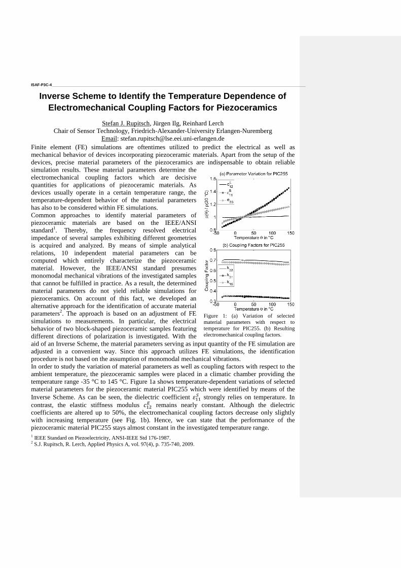
ISAF-P3C-4 _____________________________________________________________________________________________________________________
Inverse Scheme to Identify the Temperature Dependence of
Electromechanical Coupling Factors for Piezoceramics
Stefan J. Rupitsch, Jürgen Ilg, Reinhard Lerch
Chair of Sensor Technology, Friedrich-Alexander-University Erlangen-Nuremberg
Email: [email protected]
Finite element (FE) simulations are oftentimes utilized to predict the electrical as well as
mechanical behavior of devices incorporating piezoceramic materials. Apart from the setup of the
devices, precise material parameters of the piezoceramics are indispensable to obtain reliable
simulation results. These material parameters determine the
electromechanical coupling factors which are decisive
quantities for applications of piezoceramic materials. As
devices usually operate in a certain temperature range, the
temperature-dependent behavior of the material parameters
has also to be considered within FE simulations.
Common approaches to identify material parameters of
piezoceramic materials are based on the IEEE/ANSI
standard1. Thereby, the frequency resolved electrical
impedance of several samples exhibiting different geometries
is acquired and analyzed. By means of simple analytical
relations, 10 independent material parameters can be
computed which entirely characterize the piezoceramic
material. However, the IEEE/ANSI standard presumes
monomodal mechanical vibrations of the investigated samples
that cannot be fulfilled in practice. As a result, the determined
material parameters do not yield reliable simulations for
piezoceramics. On account of this fact, we developed an
alternative approach for the identification of accurate material
parameters2. The approach is based on an adjustment of FE
simulations to measurements. In particular, the electrical
behavior of two block-shaped piezoceramic samples featuring
different directions of polarization is investigated. With the
aid of an Inverse Scheme, the material parameters serving as input quantity of the FE simulation are
adjusted in a convenient way. Since this approach utilizes FE simulations, the identification
procedure is not based on the assumption of monomodal mechanical vibrations.
In order to study the variation of material parameters as well as coupling factors with respect to the
ambient temperature, the piezoceramic samples were placed in a climatic chamber providing the
temperature range -35 °C to 145 °C. Figure 1a shows temperature-dependent variations of selected
material parameters for the piezoceramic material PIC255 which were identified by means of the
Inverse Scheme. As can be seen, the dielectric coefficient strongly relies on temperature. In
contrast, the elastic stiffness modulus remains nearly constant. Although the dielectric
coefficients are altered up to 50%, the electromechanical coupling factors decrease only slightly
with increasing temperature (see Fig. 1b). Hence, we can state that the performance of the
piezoceramic material PIC255 stays almost constant in the investigated temperature range. 1 IEEE Standard on Piezoelectricity, ANSI-IEEE Std 176-1987.
2 S.J. Rupitsch, R. Lerch, Applied Physics A, vol. 97(4), p. 735-740, 2009.
Figure 1: (a) Variation of selected
material parameters with respect to
temperature for PIC255. (b) Resulting
electromechanical coupling factors.
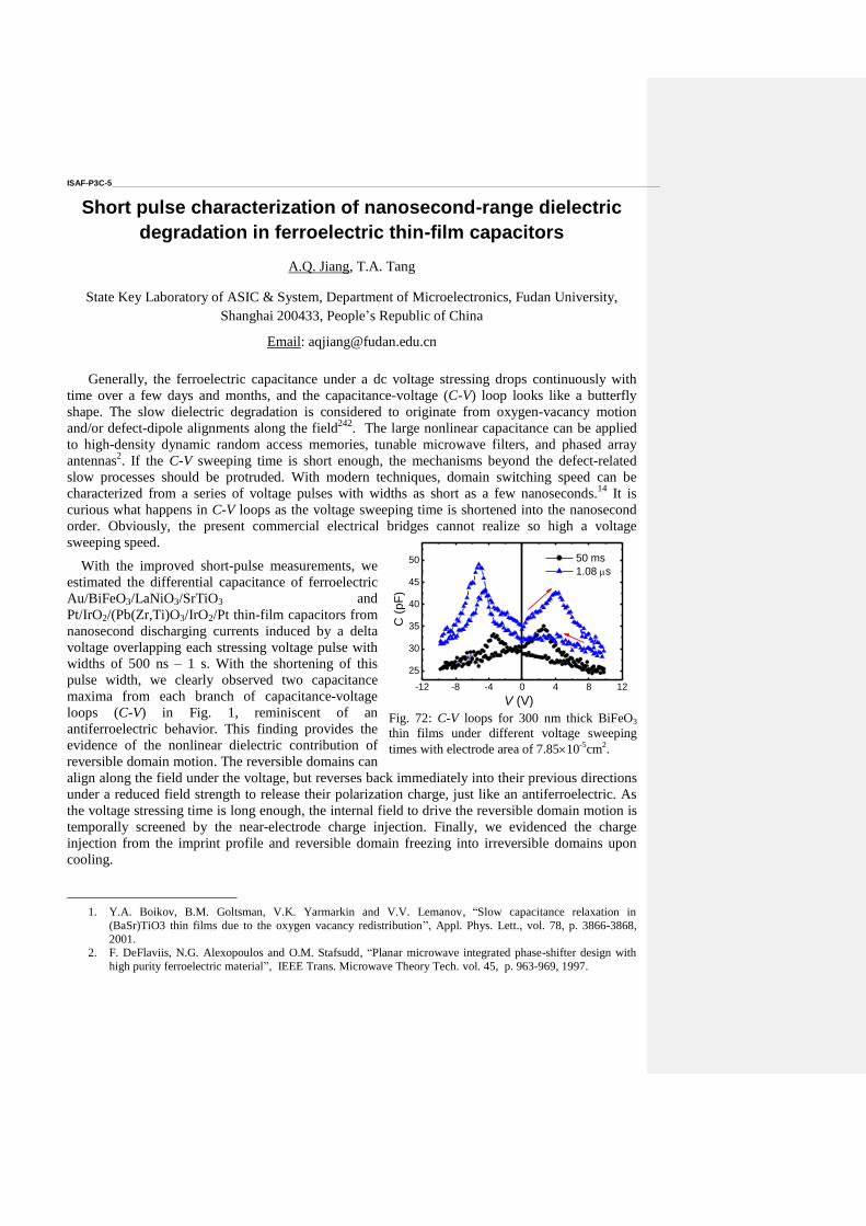
ISAF-P3C-5 _____________________________________________________________________________________________________________________
Short pulse characterization of nanosecond-range dielectric
degradation in ferroelectric thin-film capacitors
A.Q. Jiang, T.A. Tang
State Key Laboratory of ASIC & System, Department of Microelectronics, Fudan University,
Shanghai 200433, People’s Republic of China
Email: [email protected]
Generally, the ferroelectric capacitance under a dc voltage stressing drops continuously with
time over a few days and months, and the capacitance-voltage (C-V) loop looks like a butterfly
shape. The slow dielectric degradation is considered to originate from oxygen-vacancy motion
and/or defect-dipole alignments along the field242
. The large nonlinear capacitance can be applied
to high-density dynamic random access memories, tunable microwave filters, and phased array
antennas2. If the C-V sweeping time is short enough, the mechanisms beyond the defect-related
slow processes should be protruded. With modern techniques, domain switching speed can be
characterized from a series of voltage pulses with widths as short as a few nanoseconds.14
It is
curious what happens in C-V loops as the voltage sweeping time is shortened into the nanosecond
order. Obviously, the present commercial electrical bridges cannot realize so high a voltage
sweeping speed.
With the improved short-pulse measurements, we
estimated the differential capacitance of ferroelectric
Au/BiFeO3/LaNiO3/SrTiO3 and
Pt/IrO2/(Pb(Zr,Ti)O3/IrO2/Pt thin-film capacitors from
nanosecond discharging currents induced by a delta
voltage overlapping each stressing voltage pulse with
widths of 500 ns – 1 s. With the shortening of this
pulse width, we clearly observed two capacitance
maxima from each branch of capacitance-voltage
loops (C-V) in Fig. 1, reminiscent of an
antiferroelectric behavior. This finding provides the
evidence of the nonlinear dielectric contribution of
reversible domain motion. The reversible domains can
align along the field under the voltage, but reverses back immediately into their previous directions
under a reduced field strength to release their polarization charge, just like an antiferroelectric. As
the voltage stressing time is long enough, the internal field to drive the reversible domain motion is
temporally screened by the near-electrode charge injection. Finally, we evidenced the charge
injection from the imprint profile and reversible domain freezing into irreversible domains upon
cooling.
1. Y.A. Boikov, B.M. Goltsman, V.K. Yarmarkin and V.V. Lemanov,
“Slow capacitance relaxation in
(BaSr)TiO3 thin films due to the oxygen vacancy redistribution”, Appl. Phys. Lett., vol. 78, p. 3866-3868,
2001.
2. F. DeFlaviis, N.G. Alexopoulos and O.M. Stafsudd, “Planar microwave integrated phase-shifter design with
high purity ferroelectric material”, IEEE Trans. Microwave Theory Tech. vol. 45, p. 963-969, 1997.
-12 -8 -4 0 4 8 12
25
30
35
40
45
50
V (V)
C (
pF
)
50 ms
1.08 s
Fig. 72: C-V loops for 300 nm thick BiFeO3
thin films under different voltage sweeping
times with electrode area of 7.8510-5
cm2.

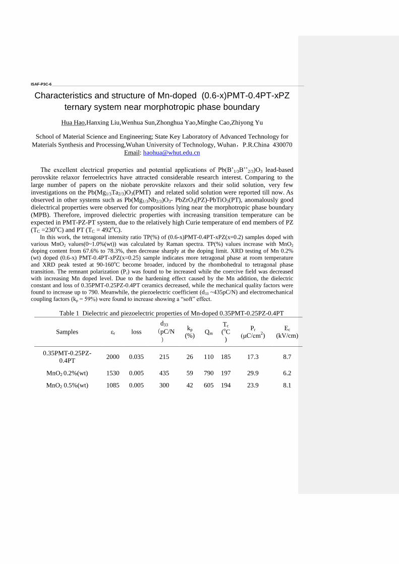
ISAF-P3C-6 _____________________________________________________________________________________________________________________
Characteristics and structure of Mn-doped (0.6-x)PMT-0.4PT-xPZ
ternary system near morphotropic phase boundary
Hua Hao,Hanxing Liu,Wenhua Sun,Zhonghua Yao,Minghe Cao,Zhiyong Yu
School of Material Science and Engineering; State Key Laboratory of Advanced Technology for
Materials Synthesis and Processing,Wuhan University of Technology, Wuhan,P.R.China 430070
Email: [email protected]
The excellent electrical properties and potential applications of Pb(B’1/3B’’2/3)O3 lead-based
perovskite relaxor ferroelectrics have attracted considerable research interest. Comparing to the
large number of papers on the niobate perovskite relaxors and their solid solution, very few
investigations on the Pb(Mg1/3Ta2/3)O3(PMT) and related solid solution were reported till now. As
observed in other systems such as Pb(Mg1/3Nb2/3)O3- PbZrO3(PZ)-PbTiO3(PT), anomalously good
dielectrical properties were observed for compositions lying near the morphotropic phase boundary
(MPB). Therefore, improved dielectric properties with increasing transition temperature can be
expected in PMT-PZ-PT system, due to the relatively high Curie temperature of end members of PZ
(TC =230oC) and PT (TC = 492
oC).
In this work, the tetragonal intensity ratio TP(%) of (0.6-x)PMT-0.4PT-xPZ(x=0.2) samples doped with
various MnO2 values(0~1.0%(wt)) was calculated by Raman spectra. TP(%) values increase with MnO2
doping content from 67.6% to 78.3%, then decrease sharply at the doping limit. XRD testing of Mn 0.2%
(wt) doped (0.6-x) PMT-0.4PT-xPZ(x=0.25) sample indicates more tetragonal phase at room temperature
and XRD peak tested at 90-160oC become broader, induced by the rhombohedral to tetragonal phase
transition. The remnant polarization (Pr) was found to be increased while the coercive field was decreased
with increasing Mn doped level. Due to the hardening effect caused by the Mn addition, the dielectric
constant and loss of 0.35PMT-0.25PZ-0.4PT ceramics decreased, while the mechanical quality factors were
found to increase up to 790. Meanwhile, the piezoelectric coefficient (d33 ~435pC/N) and electromechanical
coupling factors (kp = 59%) were found to increase showing a “soft” effect.
Table 1 Dielectric and piezoelectric properties of Mn-doped 0.35PMT-0.25PZ-0.4PT
Samples εr loss
d33
(pC/N
)
kp
(%) Qm
Tc
(oC
)
Pr
(μC/cm2)
Ec
(kV/cm)
0.35PMT-0.25PZ-
0.4PT 2000 0.035 215 26 110 185 17.3 8.7
MnO2 0.2%(wt) 1530 0.005 435 59 790 197 29.9 6.2
MnO2 0.5%(wt) 1085 0.005 300 42 605 194 23.9 8.1
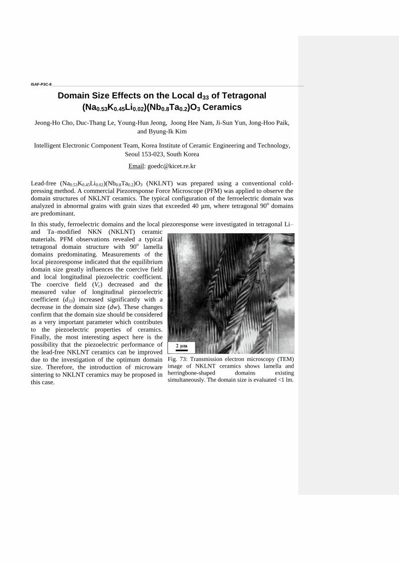
ISAF-P3C-8 _____________________________________________________________________________________________________________________
Domain Size Effects on the Local d33 of Tetragonal
(Na0.53K0.45Li0.02)(Nb0.8Ta0.2)O3 Ceramics
Jeong-Ho Cho, Duc-Thang Le, Young-Hun Jeong, Joong Hee Nam, Ji-Sun Yun, Jong-Hoo Paik,
and Byung-Ik Kim
Intelligent Electronic Component Team, Korea Institute of Ceramic Engineering and Technology,
Seoul 153-023, South Korea
Email: [email protected]
Lead-free (Na0.53K0.45Li0.02)(Nb0.8Ta0.2)O3 (NKLNT) was prepared using a conventional cold-
pressing method. A commercial Piezoresponse Force Microscope (PFM) was applied to observe the
domain structures of NKLNT ceramics. The typical configuration of the ferroelectric domain was
analyzed in abnormal grains with grain sizes that exceeded 40 µm, where tetragonal 90o domains
are predominant.
In this study, ferroelectric domains and the local piezoresponse were investigated in tetragonal Li–
and Ta–modified NKN (NKLNT) ceramic
materials. PFM observations revealed a typical
tetragonal domain structure with 90o lamella
domains predominating. Measurements of the
local piezoresponse indicated that the equilibrium
domain size greatly influences the coercive field
and local longitudinal piezoelectric coefficient.
The coercive field (Vc) decreased and the
measured value of longitudinal piezoelectric
coefficient (d33) increased significantly with a
decrease in the domain size (dw). These changes
confirm that the domain size should be considered
as a very important parameter which contributes
to the piezoelectric properties of ceramics.
Finally, the most interesting aspect here is the
possibility that the piezoelectric performance of
the lead-free NKLNT ceramics can be improved
due to the investigation of the optimum domain
size. Therefore, the introduction of microware
sintering to NKLNT ceramics may be proposed in
this case.
Fig. 73: Transmission electron microscopy (TEM)
image of NKLNT ceramics shows lamella and
herringbone-shaped domains existing
simultaneously. The domain size is evaluated <1 lm.
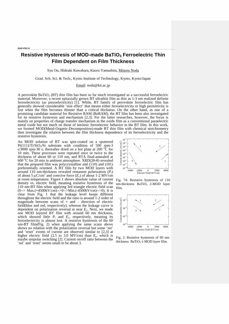
ISAF-P3C-9 _____________________________________________________________________________________________________________________
Resistive Hysteresis of MOD-made BaTiO3 Ferroelectric Thin
Film Dependent on Film Thickness
Syu Ou, Hideaki Kawahara, Kaoru Yamashita, Minoru Noda
Grad. Sch. Sci. & Tech., Kyoto Institute of Technology, Kyoto, Kyoto/Japan
Email: [email protected]
A perovskite BaTiO3 (BT) thin film has been so far much investigated as a successful ferroelectric material. Moreover, a recent epitaxially grown BT ultrathin film as thin as 1-3 nm realized definite ferroelectricity (as piezoelectricity) [1]. While, BT family of perovskite ferroelectric film has generally showed considerable ‘size effect’ that means either ferroelectricity or high permittivity is lost when the film becomes thinner than a critical thickness. On the other hand, as one of a promising candidate material for Resistive RAM (ReRAM), the BT film has been also investigated for its resistive hysteresis and mechanism [2,3]. For the latter researches, however, the focus is mainly on properties of charge transfer mechanism in the oxide film as a conventional paraelectric metal oxide but not much on those of intrinsic ferroelectric behavior in the BT film. In this work, we formed MOD(Metal-Organic-Decomposition)-made BT thin film with chemical stoichiometry then investigate the relation between the film thickness dependence of its ferroelectricity and the resistive hysteresis.
An MOD solution of BT was spin-coated on a sputtered Pt(111)/Ti/SiO2/Si substrate with condition of 500 rpm-3 s/3000 rpm-30 s, thereafter dried on a hot plate at 200
oC for
10 min. These processes were repeated once or twice to the thickness of about 60 or 110 nm, and RTA final-annealed at 600
oC for 20 min in ambient atmosphere. XRD(2-) revealed
that the prepared film was polycrystalline and (110) and (101) preferentially oriented. A BT film by two MOD layers with around 110 nm-thickness revealed remanent polarization (Pr) of about 5 C/cm
2 and coercive force (Ec) of about 1-2 MV/cm
at room temperature. Figure 1 shows absolute value of current density vs. electric field, meaning resistive hysteresis of the 110 nm-BT film when applying 3rd triangle electric field scan (0--> Max.(+4500kV/cm)-->0-->Min.(-4500kV/cm)-->0). It is clear from Fig. 1 that the leakage level keeps different throughout the electric field and the ratio is around 1-2 order of magnitude between scans of + and – direction of electric field(blue and red, respectively), whereas the leakage curve is dependent on polarization reversal at near Ec. Next, we made one MOD layered BT film with around 60 nm thickness, which showed little Pr and Ec, respectively, meaning its ferroelectricity is almost lost. A resistive hysteresis of the 60 nm-BT film(Fig. 2) when applying the same scans above shows no relation with the polarization reversal but some ‘set’ and ‘reset’ events of current are observed similar to [2,3] at higher electric field (2.5 to 3.0 MV/cm) than Ec, which is maybe unipolar switching [2]. Current on/off ratio between the ‘set’ and ‘reset’ seems small to be about 3.
-4000 -2000 0 2000 400010-10
10-9
10-8
10-7
10-6
10-5
10-4
10-3
10-2
Curr
ent
densi
ty (
A/c
m2)
Electric Field (kV/cm)
1
23
4
Fig. 74: Resistive hysteresis of 110
nm-thickness BaTiO3 2-MOD layer
film.
-4000 -2000 0 2000 400010-6
10-5
10-4
10-3
Curr
en
t d
en
sity
(A
/cm
2)
Electric Field (kV/cm)
1
23
4
Fig. 2: Resistive hysteresis of 60 nm-
thickness BaTiO3 1-MOD layer film.

Therefore, it is thought from the results that the current on/off ratio is much larger for 110 nm-BT than for 60 nm-BT. This indicates a possibility that the existence of ferroelectricity relates to the on/off ratio in the resistive hysteresis phenomena of BT thin film.
ISAF-P3C-10 ____________________________________________________________________________________________________________________
Effect of polarization switching on the electron emission of PZST
antiferroelectric ceramic
Yang Liu,1,2
Yujun Feng,1 Hongliang He,
2 and Zhuo Xu
1
1Electronic Materials Research Laboratory, Key Laboratory of the Ministry of Education &
International Center for Dielectric Research, Xi’an Jiaotong University, Xi’an 710049, China
2National Key Laboratory of Shock Wave and Detonation Physics, Institute of Fluid Physics,
CAEP, Mianyang 621900, People’s Republic of China
Email: [email protected]
Abstract
Stable pulse electric-field-induced electron emissions from antiferroelectric cathode material lead
zirconate stannate titanate (PZST) have been investigated. According to the same composition, we
analyzed the results of three different pulse-loading types. For antiferroelectric, the polarization
change could be written asA SP P , where A and SP defined, respectively, the polarization
switching factor and the saturated polarization. For ferroelectric (the orientation of polarization was
codirectional with the positive pulse), the polarization changeB ( - )S rP P P , where rP referred
remnant polarization. For ferroelectric (the orientation of polarization was reverse with the same
pulse), the polarization change ( )C S rP P P . It was found that the emission charges which were
gotten from the emission current waveforms were increasing with the polarization switching factor
i decreasing. The results may give an insight into the physical mechanism underlying the emission
process.
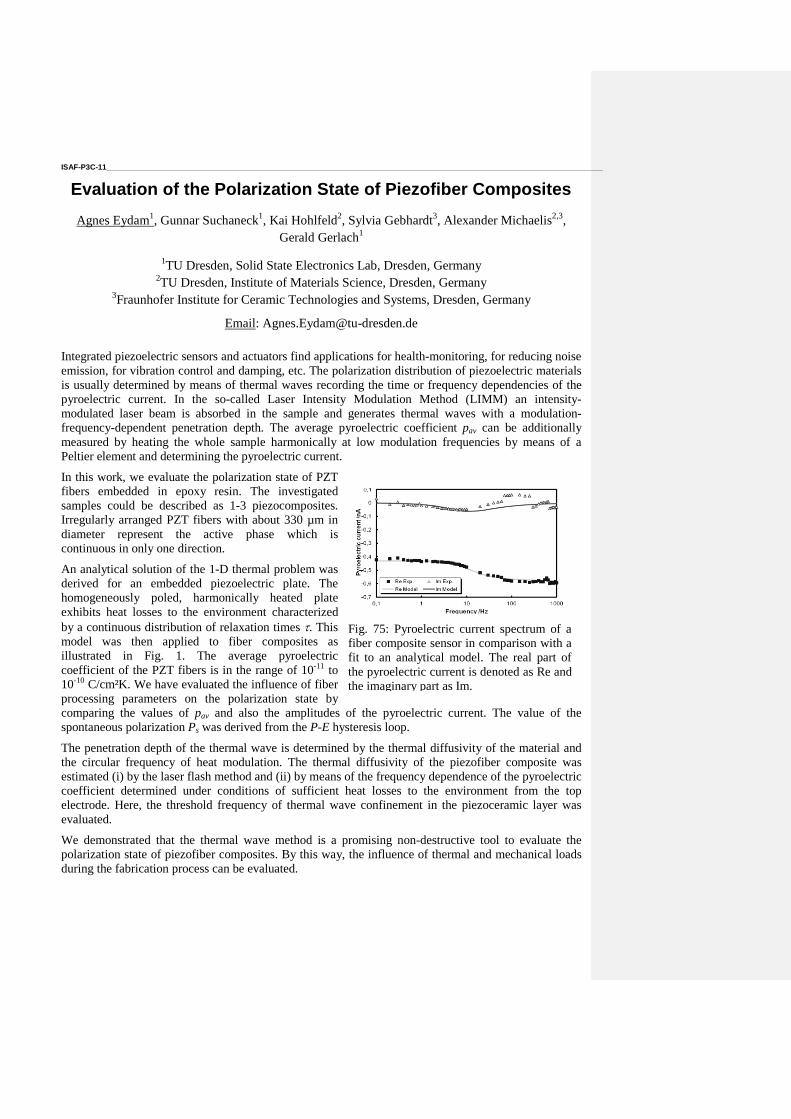
ISAF-P3C-11 ____________________________________________________________________________________________________________________
Evaluation of the Polarization State of Piezofiber Composites
Agnes Eydam1, Gunnar Suchaneck
1, Kai Hohlfeld
2, Sylvia Gebhardt
3, Alexander Michaelis
2,3,
Gerald Gerlach1
1TU Dresden, Solid State Electronics Lab, Dresden, Germany
2TU Dresden, Institute of Materials Science, Dresden, Germany
3Fraunhofer Institute for Ceramic Technologies and Systems, Dresden, Germany
Email: [email protected]
Integrated piezoelectric sensors and actuators find applications for health-monitoring, for reducing noise
emission, for vibration control and damping, etc. The polarization distribution of piezoelectric materials
is usually determined by means of thermal waves recording the time or frequency dependencies of the
pyroelectric current. In the so-called Laser Intensity Modulation Method (LIMM) an intensity-
modulated laser beam is absorbed in the sample and generates thermal waves with a modulation-
frequency-dependent penetration depth. The average pyroelectric coefficient pav can be additionally
measured by heating the whole sample harmonically at low modulation frequencies by means of a
Peltier element and determining the pyroelectric current.
In this work, we evaluate the polarization state of PZT
fibers embedded in epoxy resin. The investigated
samples could be described as 1-3 piezocomposites.
Irregularly arranged PZT fibers with about 330 µm in
diameter represent the active phase which is
continuous in only one direction.
An analytical solution of the 1-D thermal problem was
derived for an embedded piezoelectric plate. The
homogeneously poled, harmonically heated plate
exhibits heat losses to the environment characterized
by a continuous distribution of relaxation times . This
model was then applied to fiber composites as
illustrated in Fig. 1. The average pyroelectric
coefficient of the PZT fibers is in the range of 10-11 to
10-10 C/cm²K. We have evaluated the influence of fiber
processing parameters on the polarization state by
comparing the values of pav and also the amplitudes of the pyroelectric current. The value of the
spontaneous polarization Ps was derived from the P-E hysteresis loop.
The penetration depth of the thermal wave is determined by the thermal diffusivity of the material and
the circular frequency of heat modulation. The thermal diffusivity of the piezofiber composite was
estimated (i) by the laser flash method and (ii) by means of the frequency dependence of the pyroelectric
coefficient determined under conditions of sufficient heat losses to the environment from the top
electrode. Here, the threshold frequency of thermal wave confinement in the piezoceramic layer was
evaluated.
We demonstrated that the thermal wave method is a promising non-destructive tool to evaluate the
polarization state of piezofiber composites. By this way, the influence of thermal and mechanical loads
during the fabrication process can be evaluated.
Fig. 75: Pyroelectric current spectrum of a
fiber composite sensor in comparison with a
fit to an analytical model. The real part of
the pyroelectric current is denoted as Re and
the imaginary part as Im.
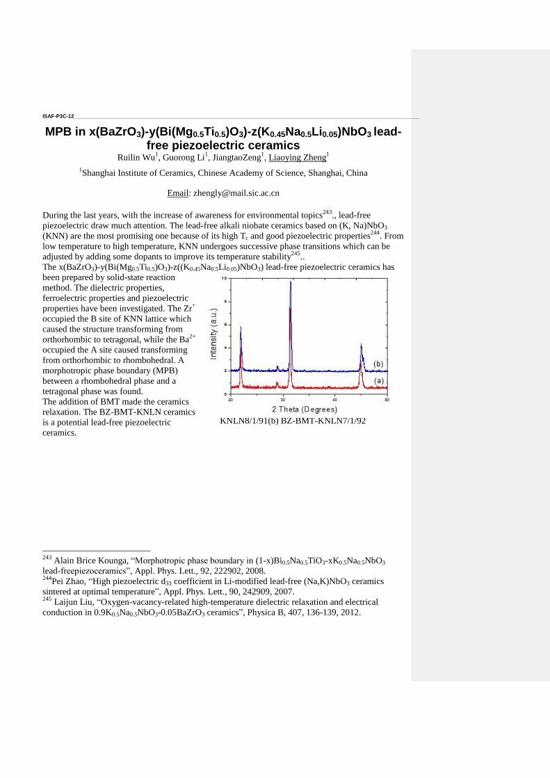
ISAF-P3C-12 ____________________________________________________________________________________________________________________
MPB in x(BaZrO3)-y(Bi(Mg0.5Ti0.5)O3)-z(K0.45Na0.5Li0.05)NbO3 lead-free piezoelectric ceramics
Ruilin Wu1, Guorong Li
1, JiangtaoZeng
1, Liaoying Zheng
1
1Shanghai Institute of Ceramics, Chinese Academy of Science, Shanghai, China
Email: [email protected]
During the last years, with the increase of awareness for environmental topics243
., lead-free
piezoelectric draw much attention. The lead-free alkali niobate ceramics based on (K, Na)NbO3
(KNN) are the most promising one because of its high Tc and good piezoelectric properties244
. From
low temperature to high temperature, KNN undergoes successive phase transitions which can be
adjusted by adding some dopants to improve its temperature stability245
..
The x(BaZrO3)-y(Bi(Mg0.5Ti0.5)O3)-z((K0.45Na0.5Li0.05)NbO3) lead-free piezoelectric ceramics has
been prepared by solid-state reaction
method. The dielectric properties,
ferroelectric properties and piezoelectric
properties have been investigated. The Zr+
occupied the B site of KNN lattice which
caused the structure transforming from
orthorhombic to tetragonal, while the Ba2+
occupied the A site caused transforming
from orthorhombic to rhombohedral. A
morphotropic phase boundary (MPB)
between a rhombohedral phase and a
tetragonal phase was found.
The addition of BMT made the ceramics
relaxation. The BZ-BMT-KNLN ceramics
is a potential lead-free piezoelectric
ceramics.
243
Alain Brice Kounga, “Morphotropic phase boundary in (1-x)Bi0.5Na0.5TiO3-xK0.5Na0.5NbO3
lead-freepiezoceramics”, Appl. Phys. Lett., 92, 222902, 2008. 244
Pei Zhao, “High piezoelectric d33 coefficient in Li-modified lead-free (Na,K)NbO3 ceramics
sintered at optimal temperature”, Appl. Phys. Lett., 90, 242909, 2007. 245
Laijun Liu, “Oxygen-vacancy-related high-temperature dielectric relaxation and electrical
conduction in 0.9K0.5Na0.5NbO3-0.05BaZrO3 ceramics”, Physica B, 407, 136-139, 2012.
Fig.76: XRD patterns of the BZ-BMT-KNLN
ceramics at room temperature.(a)BZ-BMT-
KNLN8/1/91(b) BZ-BMT-KNLN7/1/92
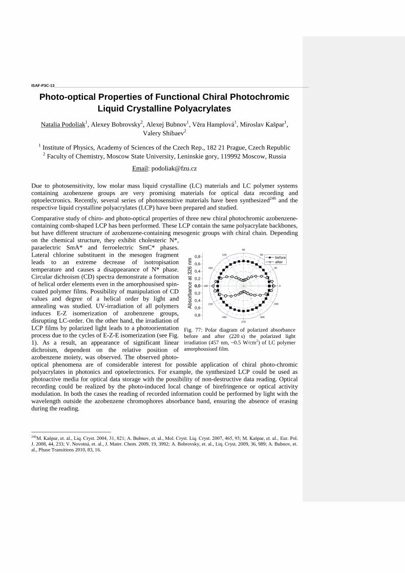
ISAF-P3C-13 ____________________________________________________________________________________________________________________
Photo-optical Properties of Functional Chiral Photochromic
Liquid Crystalline Polyacrylates
Natalia Podoliak1, Alexey Bobrovsky
2, Alexej Bubnov
1, Vĕra Hamplová
1, Miroslav Kašpar
1,
Valery Shibaev2
1 Institute of Physics, Academy of Sciences of the Czech Rep., 182 21 Prague, Czech Republic 2 Faculty of Chemistry, Moscow State University, Leninskie gory, 119992 Moscow, Russia
Email: [email protected]
Due to photosensitivity, low molar mass liquid crystalline (LC) materials and LC polymer systems
containing azobenzene groups are very promising materials for optical data recording and
optoelectronics. Recently, several series of photosensitive materials have been synthesized246 and the
respective liquid crystalline polyacrylates (LCP) have been prepared and studied.
Comparative study of chiro- and photo-optical properties of three new chiral photochromic azobenzene-
containing comb-shaped LCP has been performed. These LCP contain the same polyacrylate backbones,
but have different structure of azobenzene-containing mesogenic groups with chiral chain. Depending
on the chemical structure, they exhibit cholesteric N*,
paraelectric SmA* and ferroelectric SmC* phases.
Lateral chlorine substituent in the mesogen fragment
leads to an extreme decrease of isotropisation
temperature and causes a disappearance of N* phase.
Circular dichroism (CD) spectra demonstrate a formation
of helical order elements even in the amorphousised spin-
coated polymer films. Possibility of manipulation of CD
values and degree of a helical order by light and
annealing was studied. UV-irradiation of all polymers
induces E-Z isomerization of azobenzene groups,
disrupting LC-order. On the other hand, the irradiation of
LCP films by polarized light leads to a photoorientation
process due to the cycles of E-Z-E isomerization (see Fig.
1). As a result, an appearance of significant linear
dichroism, dependent on the relative position of
azobenzene moiety, was observed. The observed photo-
optical phenomena are of considerable interest for possible application of chiral photo-chromic
polyacrylates in photonics and optoelectronics. For example, the synthesized LCP could be used as
photoactive media for optical data storage with the possibility of non-destructive data reading. Optical
recording could be realized by the photo-induced local change of birefringence or optical activity
modulation. In both the cases the reading of recorded information could be performed by light with the
wavelength outside the azobenzene chromophores absorbance band, ensuring the absence of erasing
during the reading.
246M. Kašpar, et. al., Liq. Cryst. 2004, 31, 821; A. Bubnov, et. al., Mol. Cryst. Liq. Cryst. 2007, 465, 93; M. Kašpar, et. al., Eur. Pol.
J. 2008, 44, 233; V. Novotná, et. al., J. Mater. Chem. 2009, 19, 3992; A. Bobrovsky, et. al., Liq. Cryst. 2009, 36, 989; A. Bubnov, et.
al., Phase Transitions 2010, 83, 16.
0
30
60
90
120
150
180
210
240
270
300
330
0,0
0,2
0,4
0,6
0,8
0,0
0,2
0,4
0,6
0,8
before
after
Abso
rba
nce
at 326
nm
Fig. 77: Polar diagram of polarized absorbance
before and after (220 s) the polarized light
irradiation (457 nm, ~0.5 W/cm2) of LC polymer
amorphousised film.

This work is supported by projects: ASCR M100101204 & M100101211, CSF P204/11/0723 &
CSF 13-14133S.
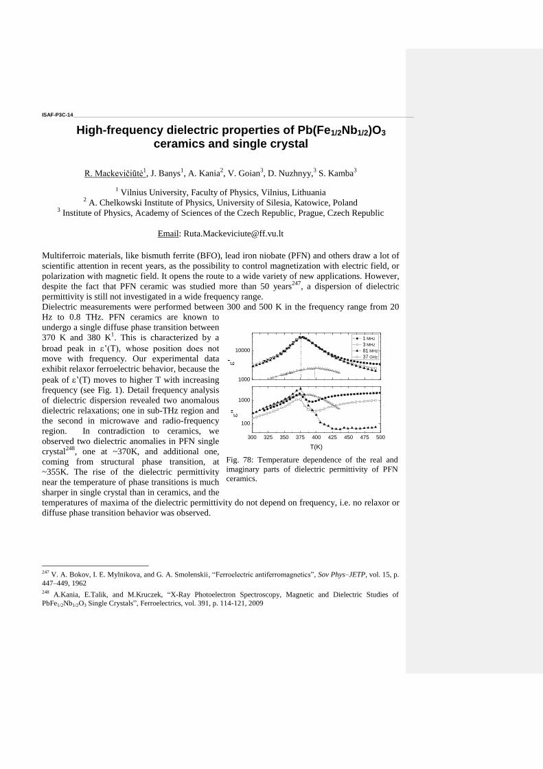
ISAF-P3C-14 ____________________________________________________________________________________________________________________
High-frequency dielectric properties of Pb(Fe1/2Nb1/2)O3
ceramics and single crystal
R. Mackevičiūtė1, J. Banys
1, A. Kania
2, V. Goian
3, D. Nuzhnyy,
3 S. Kamba
3
1 Vilnius University, Faculty of Physics, Vilnius, Lithuania
2 A. Chelkowski Institute of Physics, University of Silesia, Katowice, Poland
3 Institute of Physics, Academy of Sciences of the Czech Republic, Prague, Czech Republic
Email: [email protected]
Multiferroic materials, like bismuth ferrite (BFO), lead iron niobate (PFN) and others draw a lot of
scientific attention in recent years, as the possibility to control magnetization with electric field, or
polarization with magnetic field. It opens the route to a wide variety of new applications. However,
despite the fact that PFN ceramic was studied more than 50 years247
, a dispersion of dielectric
permittivity is still not investigated in a wide frequency range.
Dielectric measurements were performed between 300 and 500 K in the frequency range from 20
Hz to 0.8 THz. PFN ceramics are known to
undergo a single diffuse phase transition between
370 K and 380 K1. This is characterized by a
broad peak in ’(T), whose position does not
move with frequency. Our experimental data
exhibit relaxor ferroelectric behavior, because the
peak of ’(T) moves to higher T with increasing
frequency (see Fig. 1). Detail frequency analysis
of dielectric dispersion revealed two anomalous
dielectric relaxations; one in sub-THz region and
the second in microwave and radio-frequency
region. In contradiction to ceramics, we
observed two dielectric anomalies in PFN single
crystal248
, one at ~370K, and additional one,
coming from structural phase transition, at
~355K. The rise of the dielectric permittivity
near the temperature of phase transitions is much
sharper in single crystal than in ceramics, and the
temperatures of maxima of the dielectric permittivity do not depend on frequency, i.e. no relaxor or
diffuse phase transition behavior was observed.
247
V. A. Bokov, I. E. Mylnikova, and G. A. Smolenskii, “Ferroelectric antiferromagnetics”, Sov Phys–JETP, vol. 15, p.
447–449, 1962 248
A.Kania, E.Talik, and M.Kruczek, “X-Ray Photoelectron Spectroscopy, Magnetic and Dielectric Studies of
PbFe1/2Nb1/2O3 Single Crystals”, Ferroelectrics, vol. 391, p. 114-121, 2009
1000
10000
300 325 350 375 400 425 450 475 500
100
1000
1 MHz
3 MHz
81 MHz
37 GHz
'
''
T(K)
Fig. 78: Temperature dependence of the real and
imaginary parts of dielectric permittivity of PFN
ceramics.
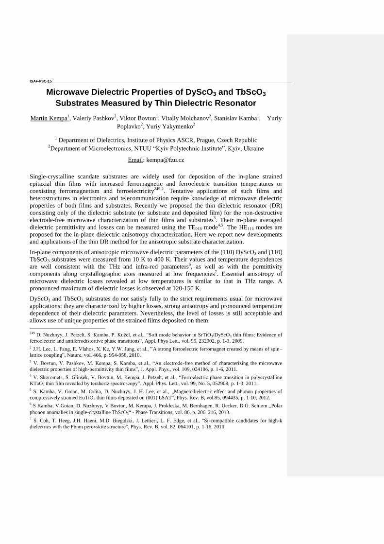
ISAF-P3C-15 ____________________________________________________________________________________________________________________
Microwave Dielectric Properties of DyScO3 and TbScO3
Substrates Measured by Thin Dielectric Resonator
Martin Kempa1, Valeriy Pashkov
2, Viktor Bovtun
1, Vitaliy Molchanov
2, Stanislav Kamba
1, Yuriy
Poplavko2, Yuriy Yakymenko
2
1 Department of Dielectrics, Institute of Physics ASCR, Prague, Czech Republic
2Department of Microelectronics, NTUU “Kyiv Polytechnic Institute”, Kyiv, Ukraine
Email: [email protected]
Single-crystalline scandate substrates are widely used for deposition of the in-plane strained
epitaxial thin films with increased ferromagnetic and ferroelectric transition temperatures or
coexisting ferromagnetism and ferroelectricity249,2
. Tentative applications of such films and
heterostructures in electronics and telecommunication require knowledge of microwave dielectric
properties of both films and substrates. Recently we proposed the thin dielectric resonator (DR)
consisting only of the dielectric substrate (or substrate and deposited film) for the non-destructive
electrode-free microwave characterization of thin films and substrates3. Their in-plane averaged
dielectric permittivity and losses can be measured using the TE01δ mode4,5
. The HE11δ modes are
proposed for the in-plane dielectric anisotropy characterization. Here we report new developments
and applications of the thin DR method for the anisotropic substrate characterization.
In-plane components of anisotropic microwave dielectric parameters of the (110) DyScO3 and (110)
TbScO3 substrates were measured from 10 K to 400 K. Their values and temperature dependences
are well consistent with the THz and infra-red parameters6, as well as with the permittivity
components along crystallographic axes measured at low frequencies7. Essential anisotropy of
microwave dielectric losses revealed at low temperatures is similar to that in THz range. A
pronounced maximum of dielectric losses is observed at 120-150 K.
DyScO3 and TbScO3 substrates do not satisfy fully to the strict requirements usual for microwave
applications: they are characterized by higher losses, strong anisotropy and pronounced temperature
dependence of their dielectric parameters. Nevertheless, the level of losses is still acceptable and
allows use of unique properties of the strained films deposited on them.
249
D. Nuzhnyy, J. Petzelt, S. Kamba, P. Kužel, et al., “Soft mode behavior in SrTiO3/DyScO3 thin films: Evidence of
ferroelectric and antiferrodistortive phase transitions”, Appl. Phys Lett., vol. 95, 232902, p. 1-3, 2009. 2 J.H. Lee, L. Fang, E. Vlahos, X. Ke, Y.W. Jung, et al., ”A strong ferroelectric ferromagnet created by means of spin–
lattice coupling”, Nature, vol. 466, p. 954-958, 2010. 3 V. Bovtun, V. Pashkov, M. Kempa, S. Kamba, et al., “An electrode-free method of characterizing the microwave
dielectric properties of high-permittivity thin films”, J. Appl. Phys., vol. 109, 024106, p. 1-6, 2011. 4 V. Skoromets, S. Glinšek, V. Bovtun, M. Kempa, J. Petzelt, et al., “Ferroelectric phase transition in polycrystalline
KTaO3 thin film revealed by terahertz spectroscopy”, Appl. Phys. Lett., vol. 99, No. 5, 052908, p. 1-3, 2011. 5 S. Kamba, V. Goian, M. Orlita, D. Nuzhnyy, J. H. Lee, et al., „Magnetodielectric effect and phonon properties of
compressively strained EuTiO3 thin films deposited on (001) LSAT“, Phys. Rev. B, vol.85, 094435, p. 1-10, 2012. 6 S Kamba, V Goian, D. Nuzhnyy, V Bovtun, M. Kempa, J. Prokleska, M. Bernhagen, R. Uecker, D.G. Schlom „Polar
phonon anomalies in single-crystalline TbScO3“ - Phase Transitions, vol. 86, p. 206–216, 2013. 7 S. Coh, T. Heeg, J.H. Haeni, M.D. Biegalski, J. Lettieri, L. F. Edge, et al., “Si-compatible candidates for high-k
dielectrics with the Pbnm perovskite structure”, Phys. Rev. B, vol. 82, 064101, p. 1-16, 2010.

ISAF-P3C-16 ____________________________________________________________________________________________________________________
Lattice distortions and Raman spectra of multiferroic
heterostructures
Yuzyuk Yury1, Khabiri Gomaa
1,4, Anokhin Andrey
1,2, Bunina Olga
3, Stryukov Daniil
1,3, Golovko
Yury2, Mukhortov Vladimir
2, Shirokov Vladimir
2
1Faculty of Physics, Southern Federal University, Rostov-on-Don, Russia 2Southern Scientific Centre, Russian Academy of Sciences, Rostov-on-Don, Russia
3Research Institute of Physics, Southern Federal University, Rostov-on-Don, Russia 4Faculty of Science, Fayoum University, Fayoum, Egypt
Email: [email protected]
Multilayer films and superlattices (SLs) consisting of ferroelectric and multiferroic layers offer a very efficient way of strain engineering to design materials with enhanced magnetoelectric responses. We report on synthesis, x-ray diffraction (XRD) and Raman scattering characterization of epitaxial heterostructures containing alternating (Bi0.98Nd0.02)FeO3 (BNFO) and (Ba0.8Sr0.2TiO3) (BST) layers deposited onto (100) MgO substrates. Both layer thickness and number of deposited layers were varied with the aim to investigate the lattice strains as a function of layers thickness. XRD and Raman examinations were performed after deposition of each layer with aim to clarify transformation of the lattice distortions at each step of growth. XRD patterns of multilayer BNFO/BST heterostructures containing five relatively thick (80 nm) layers showed slightly shifted diffraction peaks of both parent materials due to their distortion. BST layers were found to be under compressive stress, while BNFO sandwiched between two BST layers is under tensile stress. Significant shift of the E(TO) soft mode corresponding to BST layers and partial depolarization in the Raman spectra of multilayer heterostructures were observed due to lattice distortions imposed by epitaxial strains. For heterostructures with the modulation periods smaller that 30 nm XRD patterns contain one central peak (00l) located midway between respective BNFO and BST peaks and so-called satellite peaks typical for modulated structures – SLs. Detailed XRD examination revealed parallel “cube-on-cube” relationship between each layer and substrate, both BST and BNFO layers are highly strained. In contrast to single BST and BNFO films and heterostructures with relatively thick BNFO/BST layers, hardening of the soft mode and significant tilts and deformation of the FeO6 octahedra occurs in SLs and the symmetric-stretching mode of FeO6 octahedra about 705 cm-1 appears in the Raman spectra. We propose that distortion in FeO6 octahedra is enforced by the epitaxial strains and induces enhanced magnetic properties recently observed250 in BNFO/BST SLs with a few-nanometers modulation periods.
250
M. S. Ivanov, N. E. Sherstyuk, E. D. Mishina, A. S. Sigov, V. M. Mukhortov, and V. T. Moshnyaga, “Enhanced
magnetization and ferroelectric switching in multiferroic BST/BNFO superstructures,” Ferroelectrics vol. 433, p. 158-
163, 2012.
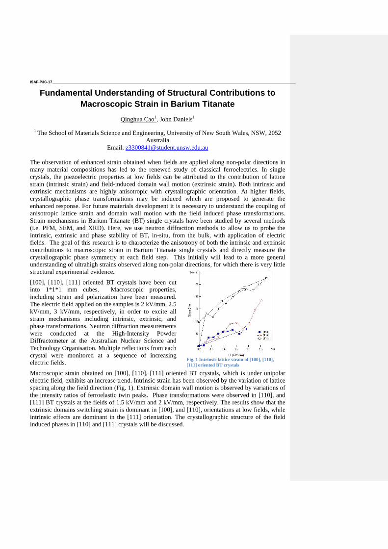
ISAF-P3C-17 ____________________________________________________________________________________________________________________
Fundamental Understanding of Structural Contributions to
Macroscopic Strain in Barium Titanate
Qinghua Cao1, John Daniels
1
1 The School of Materials Science and Engineering, University of New South Wales, NSW, 2052
Australia
Email: [email protected]
The observation of enhanced strain obtained when fields are applied along non-polar directions in
many material compositions has led to the renewed study of classical ferroelectrics. In single
crystals, the piezoelectric properties at low fields can be attributed to the contribution of lattice
strain (intrinsic strain) and field-induced domain wall motion (extrinsic strain). Both intrinsic and
extrinsic mechanisms are highly anisotropic with crystallographic orientation. At higher fields,
crystallographic phase transformations may be induced which are proposed to generate the
enhanced response. For future materials development it is necessary to understand the coupling of
anisotropic lattice strain and domain wall motion with the field induced phase transformations.
Strain mechanisms in Barium Titanate (BT) single crystals have been studied by several methods
(i.e. PFM, SEM, and XRD). Here, we use neutron diffraction methods to allow us to probe the
intrinsic, extrinsic and phase stability of BT, in-situ, from the bulk, with application of electric
fields. The goal of this research is to characterize the anisotropy of both the intrinsic and extrinsic
contributions to macroscopic strain in Barium Titanate single crystals and directly measure the
crystallographic phase symmetry at each field step. This initially will lead to a more general
understanding of ultrahigh strains observed along non-polar directions, for which there is very little
structural experimental evidence.
[100], [110], [111] oriented BT crystals have been cut
into 1*1*1 mm cubes. Macroscopic properties,
including strain and polarization have been measured.
The electric field applied on the samples is 2 kV/mm, 2.5
kV/mm, 3 kV/mm, respectively, in order to excite all
strain mechanisms including intrinsic, extrinsic, and
phase transformations. Neutron diffraction measurements
were conducted at the High-Intensity Powder
Diffractometer at the Australian Nuclear Science and
Technology Organisation. Multiple reflections from each
crystal were monitored at a sequence of increasing
electric fields.
Macroscopic strain obtained on [100], [110], [111] oriented BT crystals, which is under unipolar
electric field, exhibits an increase trend. Intrinsic strain has been observed by the variation of lattice
spacing along the field direction (Fig. 1). Extrinsic domain wall motion is observed by variations of
the intensity ratios of ferroelastic twin peaks. Phase transformations were observed in [110], and
[111] BT crystals at the fields of 1.5 kV/mm and 2 kV/mm, respectively. The results show that the
extrinsic domains switching strain is dominant in [100], and [110], orientations at low fields, while
intrinsic effects are dominant in the [111] orientation. The crystallographic structure of the field
induced phases in [110] and [111] crystals will be discussed.
Fig. 1 Intrinsic lattice strain of [100], [110],
[111] oriented BT crystals

ISAF-P3C-18 ____________________________________________________________________________________________________________________
Formation Mechanism and Dielectric Properties of the KTiNbO5 and
K3Ti5NbO14 Ceramics Mir Im
1, Sang-Hyo Kweon
1, Guifang Han
1, Sahn Nahm
a,1, Ji-Won Choi
2 and Seong-Ju Hwang
3
1Department of Materials Science and Engineering, Korea University, Seoul 136-701, South
Korea
2Electronic Materials Center, KIST 39-1 Hawolkok-dong, Seongbuk-gu, Seoul 137-791, South
Korea
3Center for Intelligent Nano-Bio Materials (CINBM), Department of Chemistry and Nano
Sciences, Ewha Womans University, Seoul 120-750, South Korea
Email: [email protected]
TiNbO5 and Ti5NbO14 nano-films synthesized by KTiNbO5 and K3Ti5NbO14-layered compounds,
respectively, have been reported to exhibit a high εr with a low leakage current density.[1] Although
their dielectric properties have been reported, their structural and dielectric properties have not been
clearly investigated.[2] In order to fabricate a nano-film having good dielectric properties, it is
necessary to understand the microstructure and dielectric properties of the bulk layered perovskite
compounds. In this work, therefore, the formation process, the microstructure and dielectric
properties of the KTiNbO5 and the K3Ti5NbO14 oxides are systematically studied. A homogeneous
KTiNbO5 and K3Ti5NbO14 phases were formed at 900oC and the dense KTiNbO5 and K3Ti5NbO14
ceramics were obtained from the specimen sintered at 1150oC and 1125
oC, respectively. Liquid-
phase-assisted abnormal grain growth occurred in both specimens along the directions
perpendicular to <002> during the sintering. Moreover, the secondary phases were developed in the
specimens sintered at high temperatures due to the evaporation of K2O. The KTiNbO5 and
K3Ti5NbO14 ceramics oxides sintered at 1150oC and 1125
oC, respectively, showed the highest
relative density of 96.0 % and 96.9% of the theoretical density. The detailed formation processes of
the KTiNbO5 and K3Ti5NbO14 ceramics and their dielectric properties will be also discussed in this
work.
ISAF-P3C-19 ____________________________________________________________________________________________________________________
Infrared and terahertz study of lattice dynamics in PbTiO3
Tetyana Ostapchuk1, Christelle Kadlec
1, Petr Kužel
1, Jiří Hlinka
1, and Antoni Kania
2
1Department of Dielectrics, Institute of Physics, Academy of Sciences of the Czech Republic,
18221 Prague 8, Czech Republic 2Institute of Physics, University of Silesia, Uniwersytecka 4, 40007 Katowice, Poland
Email: [email protected]
Recent success in understanding of the dynamics of the ferroelectric transition in PbTiO3xxiv,xxv
still
requires a straightforward interconnection of the lattice modes behavior with the macroscopic
dielectric characteristics. Here we present high-frequency dielectric spectra evaluated from the far
infrared reflectivity and time-domain terahertz transmission measurements. Their analysis enabled
us not only to get a full set of the polar mode parameters from the center of the Brillouin zone but
also to estimate the contribution of the lattice vibrations in the dielectric anomaly of PbTiO3
quantitatively.
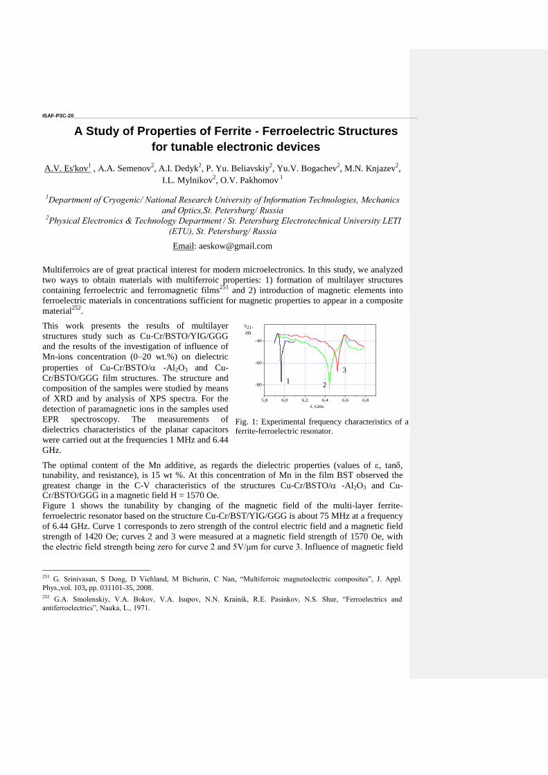
ISAF-P3C-20 ____________________________________________________________________________________________________________________
A Study of Properties of Ferrite - Ferroelectric Structures
for tunable electronic devices
A.V. Es'kov1 , А.A. Semenov
2, A.I. Dedyk
2, P. Yu. Beliavskiy
2, Yu.V. Bogachev
2, M.N. Knjazev
2,
I.L. Mylnikov2, O.V. Pakhomov
1
1Department of Cryogenic/ National Research University of Information Technologies, Mechanics
and Optics,St. Petersburg/ Russia 2
Physical Electronics & Technology Department / St. Petersburg Electrotechnical University LETI
(ETU), St. Petersburg/ Russia
Email: [email protected]
Multiferroics are of great practical interest for modern microelectronics. In this study, we analyzed
two ways to obtain materials with multiferroic properties: 1) formation of multilayer structures
containing ferroelectric and ferromagnetic films251
and 2) introduction of magnetic elements into
ferroelectric materials in concentrations sufficient for magnetic properties to appear in a composite
material252
.
This work presents the results of multilayer
structures study such as Cu-Cr/BSTO/YIG/GGG
and the results of the investigation of influence of
Mn-ions concentration (0–20 wt.%) on dielectric
properties of Cu-Cr/BSTO/ -Al2O3 and Cu-
Cr/BSTO/GGG film structures. The structure and
composition of the samples were studied by means
of XRD and by analysis of XPS spectra. For the
detection of paramagnetic ions in the samples used
EPR spectroscopy. The measurements of
dielectrics characteristics of the planar capacitors
were carried out at the frequencies 1 MHz and 6.44
GHz.
The optimal content of the Mn additive, as regards the dielectric properties (values of , tan, tunability, and resistance), is 15 wt %. At this concentration of Mn in the film BST observed the
greatest change in the C-V characteristics of the structures Cu-Cr/BSTO/ -Al2O3 and Cu-Cr/BSTO/GGG in a magnetic field H = 1570 Oe.
Figure 1 shows the tunability by changing of the magnetic field of the multi-layer ferrite-
ferroelectric resonator based on the structure Cu-Cr/BST/YIG/GGG is about 75 MHz at a frequency
of 6.44 GHz. Curve 1 corresponds to zero strength of the control electric field and a magnetic field
strength of 1420 Oe; curves 2 and 3 were measured at a magnetic field strength of 1570 Oe, with
the electric field strength being zero for curve 2 and 5V/μm for curve 3. Influence of magnetic field
251
G. Srinivasan, S Dong, D Viehland, M Bichurin, C Nan, “Multiferroic magnetoelectric composites”, J. Appl.
Phys.,vol. 103, pp. 031101-35, 2008. 252
G.A. Smolenskiy, V.A. Bokov, V.A. Isupov, N.N. Krainik, R.E. Pasinkov, N.S. Shur, “Ferroelectrics and
antiferroelectrics”, Nauka, L., 1971.
Fig. 1: Experimental frequency characteristics of a
ferrite-ferroelectric resonator.
5,8 6,0 6,2 6,4 6,6 6,8
-80
-60
-40
f, GHz
S21,
dB
1 2
3

on the C-V characteristics of investigated structures and on the tunability of the resonator associated
with magnetoelectric effect.
ISAF-P3C-21 ____________________________________________________________________________________________________________________
Structure and Multifunctionality of Strontium-Barium Niobate Dec Jan
1, Miga Seweryn
1, Wokulska Krystyna
1, Paszkowski Robert
1, Świrkowicz Marek
2,
Łukasiewicz Tadeusz2, Kleemann Wolfgang
3
1Institute of Materials Science, University of Silesia, Katowice, Poland
2Institute of Electronic Materials Technology, Warsaw, Poland
3Angewandte Physik, Universität Duisburg-Essen, Duisburg, Germany
Email: [email protected]
Solid solutions of the strontium-barium niobate SrxBa1-xNb2O6 where 0.25 < x < 0.8 (SBN) are
environmental friendly (lead free) polar materials of oxygen octahedral family. This type of
materials is recognized as very prolific due to its five different cationic crystallographic sites.
Consequently, physical characteristics of SBN are strongly correlated to composition and chemical
bonding. As a result of the compositional flexibility, SBN is recognized to exhibit diverse
properties. Correspondingly, its potential applications are based on very attractive pyroelectric,
electromechanical, electro-optic, photorefractive, and nonlinear optical and dielectric properties.
Structurally strontium-barium niobate is distinguished by its open tungsten bronze structure, i.e. the
compound contains five AB2O6 formula units per tetragonal unit cell in which six A sites are
occupied by five divalent metal ions A. As a result the empty sites give rise to quenched electric
random fields even in the stoichiometric compound. Consequently, by changing the ratio between
strontium and barium components one may tune the system from ferroelectric (x < 0.5) to a generic
relaxor (x > 0.6) behavior while maintaining the structure unchanged253
.
Using the Czochralski method eleven single crystalline compounds with nominal x = 0.26, 0.35,
0.40, 0.45, 0.50, 0.45, 0.61, 0.65, 0.70, 0.75, and 0.80 designated hereafter as SBN26, …, SBN80
have been grown. The crystals, grown along the [001] tetragonal direction, were up to 22 mm in
diameter and 40 mm in length with characteristic 24 faces, free from striations and other extended
defects. Density of etch pits was found to be of the order of 102 – 10
3 cm
-2.
Investigations of the linear dielectric response measured within 50 1010 f Hz along the polar c-
axis of the obtained single crystals reveal a gradual crossover from ferroelectric (SBN26) to utmost
relaxor-like (SBN80) behavior with a strong spatial anisotropy in the response. Complementary,
temperature dependences of the lattice parameters confirm existence of structural phase transitions
in all the investigated systems and conoscopic observations disclose an optical biaxiality for the
crystals with 0.75 x.
Financial support by MNiSW under grant N N507 455034 is gratefully acknowledged.
253
A. M. Glass, “Investigation of the Electric Properties…”, J. Appl. Phys., vol. 40, p. 4699 -4713, 1969.
ISAF-P3C-22 ____________________________________________________________________________________________________________________
Structural changes in the Y1-xCaxMnO3 solid solutions
Razumnaya A., Rudskaya A., Vlasenko M., Kupriyanov M.
Department of Physics, Southern Federal University, Rostov-on-Don, Russia
Email: [email protected]
Solid solutions are usually used with the aim to modify properties of functional material based on
Mn-containing oxides. A well-known multiferroic YMnO3 are widely used as one of the basic
components of these solid solutions. Although in recent years Y1-xCaxMnO3 solid solutions system
were studied in a number of articles254,255
, the peculiarities of their structures is not yet understood.
The main feature of these solid solutions is the occurrence of the reconstructive transition from the
hexagonal, typical for YMnO3, to orthorhombic structure at room temperature when the Ca
concentration increases.
The purpose of this work was to investigate in details the structural changes in the Y1-xCaxMnO3
solid solutions as a function of Ca concentration in order to determine symmetry of phases, ranges
of their concentration stability and variation of interatomic bond distances.
It is found that YMnO3 is characterized by hexagonal phase P63cm, as expected. It is shown that at
room temperature the concentration boundary between hexagonal P63cm and P63/mmc phases in Y1-
xCaxMnO3 solid solutions is located around x = 0.15. A reconstructive transition from hexagonal
P63/mmc phase to orthorhombic perovskite Pnma phase occurs in the concentration range
0.17 ≤ x ≤ 0.25. The compounds with x = 0.3; 0.5 belong to the orthorhombic perovskite Pnma
structure. In addition to the orthorhombic perovskite phase the cubic phase Pm3m coexists in the
sample with x = 0.7.
As known, YMnO3 can be synthesized with the perovskite type structure only at high pressure256
.
Alternatively, the formation of the perovskite phase in the Y1-xCaxMnO3 solid solutions with x ≥
0.15 occurs at normal pressure. The observed at room temperature concentration phase transition in
the Y1-xCaxMnO3 solid solutions at x ~ 0.17 from the polar P63cm to nonpolar P63/mmc phase with
the emergence of the orthorhombic perovskite Pnma phase is an evidence of complicated structural
changes.
A comparative analysis of the interatomic bond distances in the oxygen polyhedra of hexagonal and
orthorhombic perovskite structures shows that the Mn-O bond distances are close in both structures.
Thus, reconstruction does not affect the interatomic distances in oxygen polyhedra considerably.
The results of preliminary measurements of the magnetic properties of the Y1-xCaxMnO3 solid
solutions are presented. The evidences of magnetic ordering at temperatures of about 50 K have
been found.
254
M. N. Iliev, B. Lorenz, A. P. Litvinchuk, Y. Q. Wang, Y. Y. Sun, C. W. Chu, “Structural, transport, magnetic
properties and Raman spectroscopy of orthorhombic Y1−xCaxMnO3 (0≤x≤0.5)”, J. Phys.: Condens. Matter., vol. 17, p.
3333, 2005. 255
J. R. Sahu, C. R.Serrao, A. Ghost, A. Sundaresan, C. N. R. Rao, “Charge-order-driven multiferroic properties of Y1-
xCaxMnO3”, Solid State Commun., vol. 149, p. 49-51, 2009. 256
V. E. Wood, A. E. Austin, E. W. Collings, “Magnetic properties of heavy-rare-earth orthomanganites”, Phys. Chem.
Solids., vol. 34, p. 859-868, 1973.
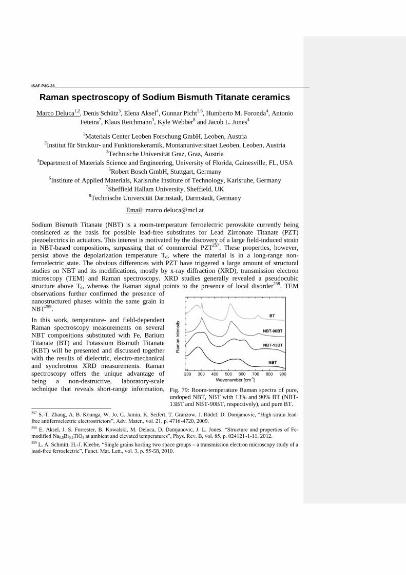
ISAF-P3C-23 ____________________________________________________________________________________________________________________
Raman spectroscopy of Sodium Bismuth Titanate ceramics
Marco Deluca1,2
, Denis Schütz3, Elena Aksel
4, Gunnar Picht
5,6, Humberto M. Foronda
4, Antonio
Feteira7, Klaus Reichmann
3, Kyle Webber
8 and Jacob L. Jones
4
1Materials Center Leoben Forschung GmbH, Leoben, Austria
2Institut für Struktur- und Funktionskeramik, Montanuniversitaet Leoben, Leoben, Austria
3Technische Universität Graz, Graz, Austria
4Department of Materials Science and Engineering, University of Florida, Gainesville, FL, USA
5Robert Bosch GmbH, Stuttgart, Germany
6Institute of Applied Materials, Karlsruhe Institute of Technology, Karlsruhe, Germany
7Sheffield Hallam University, Sheffield, UK
8Technische Universität Darmstadt, Darmstadt, Germany
Email: [email protected]
Sodium Bismuth Titanate (NBT) is a room-temperature ferroelectric perovskite currently being
considered as the basis for possible lead-free substitutes for Lead Zirconate Titanate (PZT)
piezoelectrics in actuators. This interest is motivated by the discovery of a large field-induced strain
in NBT-based compositions, surpassing that of commercial PZT257
. These properties, however,
persist above the depolarization temperature Td, where the material is in a long-range non-
ferroelectric state. The obvious differences with PZT have triggered a large amount of structural
studies on NBT and its modifications, mostly by x-ray diffraction (XRD), transmission electron
microscopy (TEM) and Raman spectroscopy. XRD studies generally revealed a pseudocubic
structure above Td, whereas the Raman signal points to the presence of local disorder258
. TEM
observations further confirmed the presence of
nanostructured phases within the same grain in
NBT259
.
In this work, temperature- and field-dependent
Raman spectroscopy measurements on several
NBT compositions substituted with Fe, Barium
Titanate (BT) and Potassium Bismuth Titanate
(KBT) will be presented and discussed together
with the results of dielectric, electro-mechanical
and synchrotron XRD measurements. Raman
spectroscopy offers the unique advantage of
being a non-destructive, laboratory-scale
technique that reveals short-range information,
257
S.-T. Zhang, A. B. Kounga, W. Jo, C. Jamin, K. Seifert, T. Granzow, J. Rödel, D. Damjanovic, “High-strain lead-
free antiferroelectric electrostrictors”, Adv. Mater., vol. 21, p. 4716-4720, 2009. 258
E. Aksel, J. S. Forrester, B. Kowalski, M. Deluca, D. Damjanovic, J. L. Jones, “Structure and properties of Fe-
modified Na0.5Bi0.5TiO3 at ambient and elevated temperatures”, Phys. Rev. B, vol. 85, p. 024121-1-11, 2012. 259
L. A. Schmitt, H.-J. Kleebe, “Single grains hosting two space groups – a transmission electron microscopy study of a
lead-free ferroelectric”, Funct. Mat. Lett., vol. 3, p. 55-58, 2010.
Fig. 79: Room-temperature Raman spectra of pure,
undoped NBT, NBT with 13% and 90% BT (NBT-
13BT and NBT-90BT, respectively), and pure BT.

complementary to the aforementioned techniques.
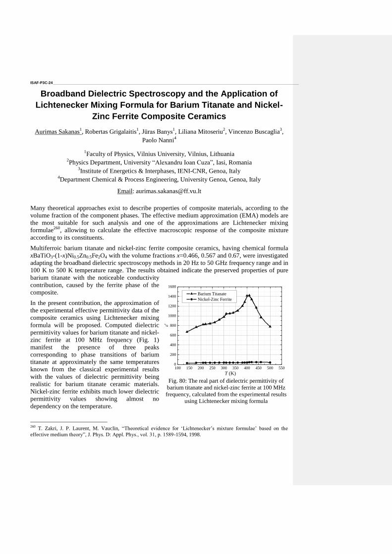
ISAF-P3C-24 ____________________________________________________________________________________________________________________
Broadband Dielectric Spectroscopy and the Application of
Lichtenecker Mixing Formula for Barium Titanate and Nickel-
Zinc Ferrite Composite Ceramics
Aurimas Sakanas1, Robertas Grigalaitis
1, Jūras Banys
1, Liliana Mitoseriu
2, Vincenzo Buscaglia
3,
Paolo Nanni4
1Faculty of Physics, Vilnius University, Vilnius, Lithuania
2Physics Department, University “Alexandru Ioan Cuza”, Iasi, Romania
3Institute of Energetics & Interphases, IENI-CNR, Genoa, Italy
4Department Chemical & Process Engineering, University Genoa, Genoa, Italy
Email: [email protected]
Many theoretical approaches exist to describe properties of composite materials, according to the
volume fraction of the component phases. The effective medium approximation (EMA) models are
the most suitable for such analysis and one of the approximations are Lichtenecker mixing
formulae260
, allowing to calculate the effective macroscopic response of the composite mixture
according to its constituents.
Multiferroic barium titanate and nickel-zinc ferrite composite ceramics, having chemical formula
xBaTiO3-(1-x)Ni0.5Zn0.5Fe2O4 with the volume fractions x=0.466, 0.567 and 0.67, were investigated
adapting the broadband dielectric spectroscopy methods in 20 Hz to 50 GHz frequency range and in
100 K to 500 K temperature range. The results obtained indicate the preserved properties of pure
barium titanate with the noticeable conductivity
contribution, caused by the ferrite phase of the
composite.
In the present contribution, the approximation of
the experimental effective permittivity data of the
composite ceramics using Lichtenecker mixing
formula will be proposed. Computed dielectric
permittivity values for barium titanate and nickel-
zinc ferrite at 100 MHz frequency (Fig. 1)
manifest the presence of three peaks
corresponding to phase transitions of barium
titanate at approximately the same temperatures
known from the classical experimental results
with the values of dielectric permittivity being
realistic for barium titanate ceramic materials.
Nickel-zinc ferrite exhibits much lower dielectric
permittivity values showing almost no
dependency on the temperature.
260
T. Zakri, J. P. Laurent, M. Vauclin, “Theoretical evidence for ‘Lichtenecker’s mixture formulae’ based on the
effective medium theory”, J. Phys. D: Appl. Phys., vol. 31, p. 1589-1594, 1998.
100 150 200 250 300 350 400 450 500 5500
200
400
600
800
1000
1200
1400
1600
Barium Titanate
Nickel-Zinc Ferrite
T (K)
'
Fig. 80: The real part of dielectric permittivity of
barium titanate and nickel-zinc ferrite at 100 MHz
frequency, calculated from the experimental results
using Lichtenecker mixing formula

ISAF-P3C-25 ____________________________________________________________________________________________________________________
LiNbO3-LiTaO3 mixed crystals:
A joint theoretical and Raman investigation S. Neufeld
1, S. Sanna
1, A. Riefer
1, M. Grothe
1, G. Berth
1, A. Zrenner
2,1,
H. Zhang3 and W. G. Schmidt
1
1Universität Paderborn, 33098 Paderborn, Germany
2Center for Optoelectronics and Photonics Paderborn (CeOPP), 33098 Paderborn, Germany
3State Key Lab of Crystal Materials, Shandong University, Jinan 250100, China
e-mail: [email protected]
Mixed crystals have recently attracted the attention of the scientific community, as they offer the
possibility to tune the physical properties by varying the composition. Lithium niobate-tantalate
(LNT) is one of the simplest ferroelectric mixed crystals, which shows quite unusual physical
properties. In particular, the existence of a composition with zero birefringence at room temperature
is unique in ferroelectric nonlinear-optical materials. Indeed within this composition the crystal is
optical isotropic and yet electrically polar [1,2].
Despite the huge potential in electro-optic and acousto-optic devices and the extensive use of the
end-compounds LN and LT, relatively few is known about the mixed crystals [3,4]. In this
contribution, we characterize LiNb1-xTaxO3 over a wide composition range by the combined
approach of first-principles simulations in the framework of the density functional theory and
Raman spectroscopy.
Structural parameters (such as volumes and lattice constants) show a Vegard-like behaviour
between the end-compounds LN and LT, while the electronic band gap shows pronounced
deviations from the linearity. Measured Raman spectra and frequencies predicted from the
theoretical models are compared. In particular, the frequency and intensity dependence of the four
A1-TO modes on the crystal composition is discussed and explained on the basis of the phonon
eigenvectors calculated within the density functional theory. Based on our result, we show that the
LNT composition can be quite accurately estimated by its vibrational properties.
[1] I. G. Wood, P. Daniels, R. H. Brown and A. M. Glazer, J. Phys.: Cond. Mat. 20, 235237 (2008).
[2] A. Bartasyte, A. M. Glazer, F. Wondre, D. Prabhakaran, P. A. Thomas, S. Huband, D. S. Keeble, S.
Margueron, Mat. Chem. Phys., 134, 728 (2012).
[3] S. Margueron, A. Bartasyte, A. M. Glazer, E. Simon, J. Hlinka, I. Gregora, and J. Gleize, J. App.
Phys. 111, 104105 (2012).
[4] D. Xue, K. Betzler, H. Hesse, Solid State Communications 115, 581(2000).
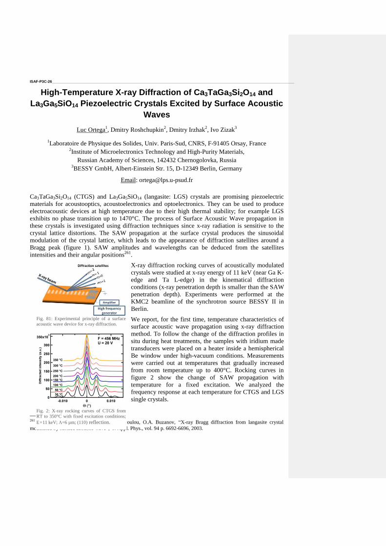
ISAF-P3C-26 ____________________________________________________________________________________________________________________
High-Temperature X-ray Diffraction of Ca3TaGa3Si2O14 and
La3Ga5SiO14 Piezoelectric Crystals Excited by Surface Acoustic
Waves
Luc Ortega1, Dmitry Roshchupkin
2, Dmitry Irzhak
2, Ivo Zizak
3
1Laboratoire de Physique des Solides, Univ. Paris-Sud, CNRS, F-91405 Orsay, France
2Institute of Microelectronics Technology and High-Purity Materials,
Russian Academy of Sciences, 142432 Chernogolovka, Russia 3BESSY GmbH, Albert-Einstein Str. 15, D-12349 Berlin, Germany
Email: [email protected]
Ca3TaGa3Si2O14 (CTGS) and La3Ga5SiO14 (langasite: LGS) crystals are promising piezoelectric
materials for acoustooptics, acoustoelectronics and optoelectronics. They can be used to produce
electroacoustic devices at high temperature due to their high thermal stability; for example LGS
exhibits no phase transition up to 1470°C. The process of Surface Acoustic Wave propagation in
these crystals is investigated using diffraction techniques since x-ray radiation is sensitive to the
crystal lattice distortions. The SAW propagation at the surface crystal produces the sinusoidal
modulation of the crystal lattice, which leads to the appearance of diffraction satellites around a
Bragg peak (figure 1). SAW amplitudes and wavelengths can be deduced from the satellites
intensities and their angular positions261
.
X-ray diffraction rocking curves of acoustically modulated
crystals were studied at x-ray energy of 11 keV (near Ga K-
edge and Ta L-edge) in the kinematical diffraction
conditions (x-ray penetration depth is smaller than the SAW
penetration depth). Experiments were performed at the
KMC2 beamline of the synchrotron source BESSY II in
Berlin.
We report, for the first time, temperature characteristics of
surface acoustic wave propagation using x-ray diffraction
method. To follow the change of the diffraction profiles in
situ during heat treatments, the samples with iridium made
transducers were placed on a heater inside a hemispherical
Be window under high-vacuum conditions. Measurements
were carried out at temperatures that gradually increased
from room temperature up to 400°C. Rocking curves in
figure 2 show the change of SAW propagation with
temperature for a fixed excitation. We analyzed the
frequency response at each temperature for CTGS and LGS
single crystals.
261
D.V. Roshchupkin, D.V. Irzhak, R. Tucoulou, O.A. Buzanov, “X-ray Bragg diffraction from langasite crystal
modulated by surface acoustic wave”, J. Appl. Phys., vol. 94 p. 6692-6696, 2003.
Fig. 81: Experimental principle of a surface
acoustic wave device for x-ray diffraction.
Fig. 2: X-ray rocking curves of CTGS from
RT to 350°C with fixed excitation conditions;
E=11 keV; =6 µm; (110) reflection.

Other SAW and piezoelectric characteristics such as the power flow angle can be determined using
this method.
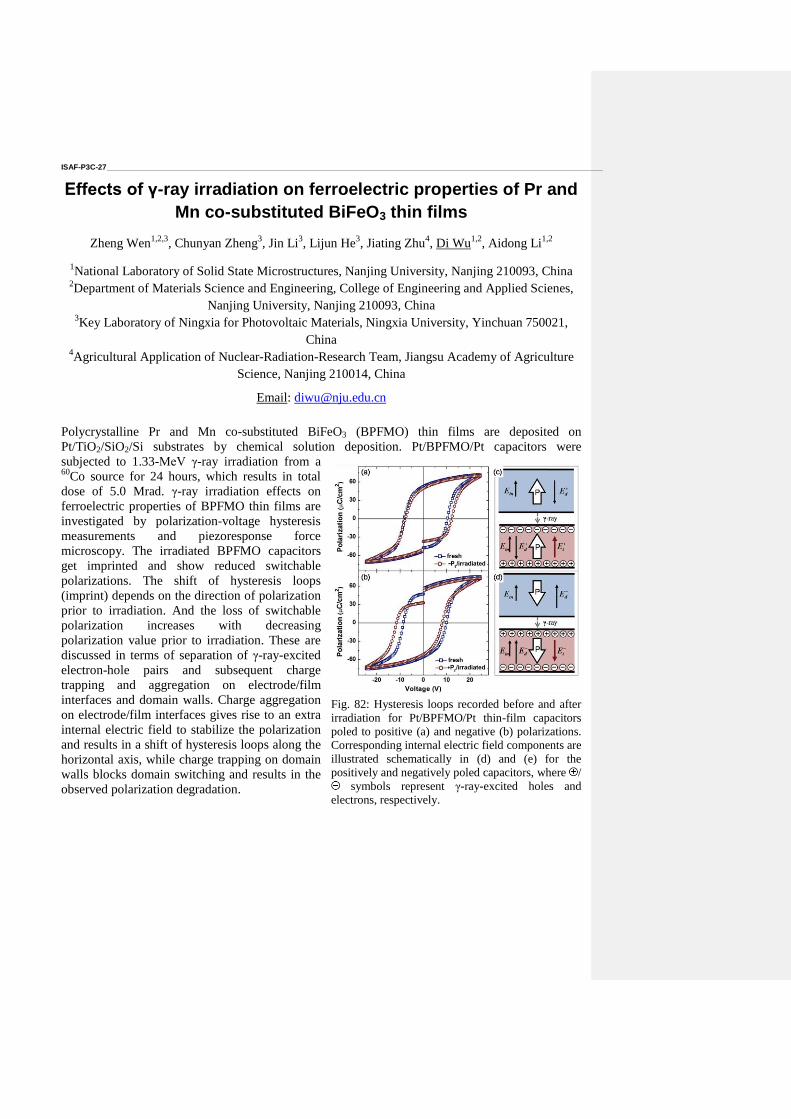
ISAF-P3C-27 ____________________________________________________________________________________________________________________
Effects of γ-ray irradiation on ferroelectric properties of Pr and
Mn co-substituted BiFeO3 thin films
Zheng Wen1,2,3
, Chunyan Zheng3, Jin Li
3, Lijun He
3, Jiating Zhu
4, Di Wu
1,2, Aidong Li
1,2
1National Laboratory of Solid State Microstructures, Nanjing University, Nanjing 210093, China
2Department of Materials Science and Engineering, College of Engineering and Applied Scienes,
Nanjing University, Nanjing 210093, China 3Key Laboratory of Ningxia for Photovoltaic Materials, Ningxia University, Yinchuan 750021,
China 4Agricultural Application of Nuclear-Radiation-Research Team, Jiangsu Academy of Agriculture
Science, Nanjing 210014, China
Email: [email protected]
Polycrystalline Pr and Mn co-substituted BiFeO3 (BPFMO) thin films are deposited on
Pt/TiO2/SiO2/Si substrates by chemical solution deposition. Pt/BPFMO/Pt capacitors were
subjected to 1.33-MeV γ-ray irradiation from a 60
Co source for 24 hours, which results in total
dose of 5.0 Mrad. γ-ray irradiation effects on
ferroelectric properties of BPFMO thin films are
investigated by polarization-voltage hysteresis
measurements and piezoresponse force
microscopy. The irradiated BPFMO capacitors
get imprinted and show reduced switchable
polarizations. The shift of hysteresis loops
(imprint) depends on the direction of polarization
prior to irradiation. And the loss of switchable
polarization increases with decreasing
polarization value prior to irradiation. These are
discussed in terms of separation of γ-ray-excited
electron-hole pairs and subsequent charge
trapping and aggregation on electrode/film
interfaces and domain walls. Charge aggregation
on electrode/film interfaces gives rise to an extra
internal electric field to stabilize the polarization
and results in a shift of hysteresis loops along the
horizontal axis, while charge trapping on domain
walls blocks domain switching and results in the
observed polarization degradation.
Fig. 82: Hysteresis loops recorded before and after
irradiation for Pt/BPFMO/Pt thin-film capacitors
poled to positive (a) and negative (b) polarizations.
Corresponding internal electric field components are
illustrated schematically in (d) and (e) for the
positively and negatively poled capacitors, where /
symbols represent γ-ray-excited holes and
electrons, respectively.
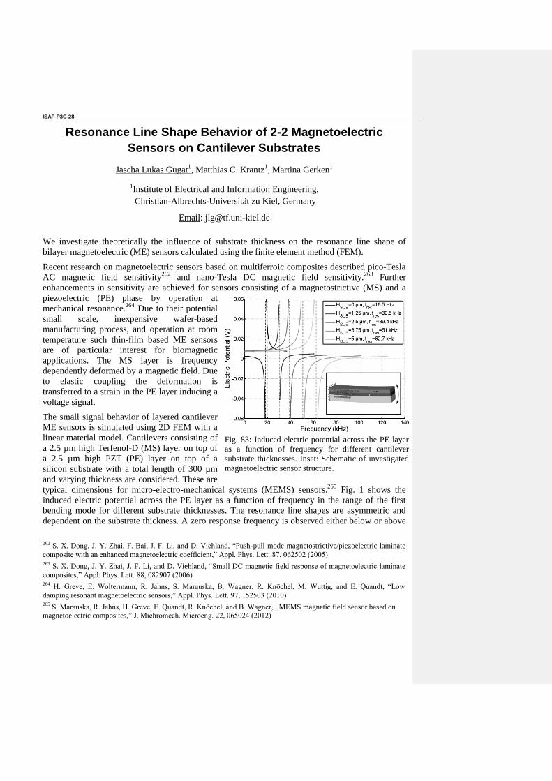
ISAF-P3C-28 ____________________________________________________________________________________________________________________
Resonance Line Shape Behavior of 2-2 Magnetoelectric
Sensors on Cantilever Substrates
Jascha Lukas Gugat1, Matthias C. Krantz
1, Martina Gerken
1
1Institute of Electrical and Information Engineering,
Christian-Albrechts-Universität zu Kiel, Germany
Email: [email protected]
We investigate theoretically the influence of substrate thickness on the resonance line shape of
bilayer magnetoelectric (ME) sensors calculated using the finite element method (FEM).
Recent research on magnetoelectric sensors based on multiferroic composites described pico-Tesla
AC magnetic field sensitivity262
and nano-Tesla DC magnetic field sensitivity.263
Further
enhancements in sensitivity are achieved for sensors consisting of a magnetostrictive (MS) and a
piezoelectric (PE) phase by operation at
mechanical resonance.264
Due to their potential
small scale, inexpensive wafer-based
manufacturing process, and operation at room
temperature such thin-film based ME sensors
are of particular interest for biomagnetic
applications. The MS layer is frequency
dependently deformed by a magnetic field. Due
to elastic coupling the deformation is
transferred to a strain in the PE layer inducing a
voltage signal.
The small signal behavior of layered cantilever
ME sensors is simulated using 2D FEM with a
linear material model. Cantilevers consisting of
a 2.5 µm high Terfenol-D (MS) layer on top of
a 2.5 µm high PZT (PE) layer on top of a
silicon substrate with a total length of 300 µm
and varying thickness are considered. These are
typical dimensions for micro-electro-mechanical systems (MEMS) sensors.265
Fig. 1 shows the
induced electric potential across the PE layer as a function of frequency in the range of the first
bending mode for different substrate thicknesses. The resonance line shapes are asymmetric and
dependent on the substrate thickness. A zero response frequency is observed either below or above
262
S. X. Dong, J. Y. Zhai, F. Bai, J. F. Li, and D. Viehland, “Push-pull mode magnetostrictive/piezoelectric laminate
composite with an enhanced magnetoelectric coefficient,” Appl. Phys. Lett. 87, 062502 (2005) 263
S. X. Dong, J. Y. Zhai, J. F. Li, and D. Viehland, “Small DC magnetic field response of magnetoelectric laminate
composites,” Appl. Phys. Lett. 88, 082907 (2006) 264
H. Greve, E. Woltermann, R. Jahns, S. Marauska, B. Wagner, R. Knöchel, M. Wuttig, and E. Quandt, “Low
damping resonant magnetoelectric sensors,” Appl. Phys. Lett. 97, 152503 (2010) 265
S. Marauska, R. Jahns, H. Greve, E. Quandt, R. Knöchel, and B. Wagner, „MEMS magnetic field sensor based on
magnetoelectric composites,” J. Michromech. Microeng. 22, 065024 (2012)
Fig. 83: Induced electric potential across the PE layer
as a function of frequency for different cantilever
substrate thicknesses. Inset: Schematic of investigated
magnetoelectric sensor structure.

the resonance frequency. These results may be explained by considering the mechanical stress and
strain distributions in the cantilever structure.
ISAF-P3C-29 ____________________________________________________________________________________________________________________
Infrared and Terahertz Spectroscopy of Epitaxial BaTiO3/SrTiO3 Superlattices
V. Železný1, Ch. Kadlec
1, A. Soukiassian
2, X.X. Xi
3, D.G. Schlom
2
1 Institute of Physics, ASCR, Na Slovance 2, 182 21 Praha 8, Czech Republic
2 Department of Materials Science and Engineering, Cornell University, Ithaca, New York, 14853-
1501, USA 3
Department of Physics, Temple University, Philadelphia, Pennsylvania 19122, USA
Email: [email protected]
Crystal lattice dynamics brings fundamental information for understanding the physical properties
of ferroelectrics. Infrared spectroscopy is a very effective tool for studying and understanding the
behavior of ferroelectrics because the incident radiation couples directly to the order parameter
(polarization). This can be used for the direct extraction of the dielectric function and determination
of the parameters important for lattice dynamics. Thin films and superlattices are more suitable for
device application, but they show difference in their behaviour compared bulk materials. Varying
temperature enables us to study nanoscale ferroelectric heterostructures in the vicinity of the phase
transition.
The infrared reflectivity and terahertz transmission measurements were performed on fully
commensurate [(BaTiO3)8/(SrTiO3)4]40 superlattices grown by molecular-beam epitaxy on scandate
substrates. The experimental spectra were measured in two polarizations along the c axis and
perpendicular to it on the (110) cut of SmScO3 substrate. The Drude-Lorentz form of the dielectric
function was used for both substrate and superlattice. First we fit the spectrum of the bare substrate
then we fixed all of its parameters. Adding the top layer to the model and fitting the total system
(substrate + superlattice), we could determine the effective parameters of the superlattice. A further
refinement of the dielectric function was done using a variational dielectric function procedure,
which provides the dielectric function in a non-parametrized form. The resulting dielectric function
is of perovskite-like character with three dominating vibration modes. Combining these approaches
enabled us to observe the soft mode and extract its parameters. The temperature behavior of the
modes and their parameters were also studied. The obtained results demonstrate that the softening
of the soft mode is much smaller than for the bulk materials of the superlattice components.
This work was partially supported by Grant Agency of the Czech Republic under Contract No.
204/11/1011.
ISAF-P3C-30 ____________________________________________________________________________________________________________________
Measurement of the indirect piezoelectric coefficient of thin
films using interferometry
Mark Stewart 1 and Markys G Cain
1
1National Physical Laboratory, Teddington, Middlesex, UK
Email: [email protected]
Piezoelectric thin films are a promising high force actuation technology for MEMS devices. At
present materials are still at the research stage, with very few Fab plants offering piezoelectric
materials as a standard option. Users and manufacturers of these films want to assess the quality of
the films at an early stage in production, so there is a requirement to be able to measure the
piezoelectric coefficient of films as produced on a substrate.
In the late 90’s Kholkin et al266
showed that many measurements of the piezoelectric output of thin
films suffered from bending effects, resulting in inflated values. To overcome this they proposed the
double beam interferometer method which became the de facto ‘standard’. More recently the
availability of microscope based laser Doppler vibrometers have led workers to re-evaluate the use
of single sided measurements, where the sample bending is eliminated by adhesive bonding to a
rigid substrate.
This work will compare both experimental methods and with the aid of FEA examine the effects of
various realistic boundary conditions on observed and predicted output.
266
A. L. Kholkin, Ch. Wütchrich, D. V. Taylor, and N. Setter, “Interferometric measurements of electric field‐induced
displacements in piezoelectric thin films”, Rev. Sci. Instrum. 67, 1935, 1996.
ISAF-P3C-31 ____________________________________________________________________________________________________________________
Hybrid improper ferroelectric phase transition in Ca3Mn2O7 S. Kamba
1, V. Goian
1, C. Adamo
2, P. Vaněk
1, J. Drahokoupil
1, A. Mould
3, H. Seiner
4,
L. Palatinus1, M. Klementová
1, M. Svatuška
1, N.A. Benedek
5, and D.G. Schlom
2,6
1Institute of Physics, Academy of Sciences of the Czech Republic, Prague, Czech Republic
2Department of Materials Science and Engineering, Cornell University, Ithaca, New York, USA
3Department of Materials Science and Engineering, University of Sheffield, Sheffield, UK
4Institute of Thermomechanics, ASCR, Prague, Czech Republic
5Materials Science and Engineering Program, The University of Texas at Austin, Texas, USA
6Kavli Institute at Cornell for Nanoscale Science, Ithaca, New York, USA
Email: [email protected]
Based on ab initio calculations, a new type of ferroelectric phase transition was recently proposed in
Ca3Mn2O7, which crystallizes in Ruddlesden-Popper structure.267
The ferroelectricity in such system
should be induced by freezing of two nonpolar phonons from Brillouin zone boundary. If the modes
of
2X and
3X symmetries will freeze simultaneously, I4/mmm phase will transform directly to
A21am orthorhombic structure and the phase transition is called the hybrid improper ferroelectric
phase transition. If the modes will freeze gradually, paraelectric I4/mmm phase should transform to
intermediate Cmcm (
3X mode freezes first) or Cmca phase (
2X mode freezes first) and after
freezing of the second parameters, the ferroelectric A21am orthorhombic structure will finally
appear. The same calculations have shown that in biaxially strained Ca3Mn2O7 films, the switching
of polarization by electric field should cause 180o flip of magnetic moments by reversing the
octahedral tilt. 267
The aim of this contribution is to determine whether Ca3Mn2O7 undergoes one hybrid or two
successive phase transitions. We have combined X-ray and electron diffraction with measurements
of thermal expansion, resonant ultrasound and infrared (IR) spectroscopy. We investigated both
bulk ceramics and strained Ca3Mn2O7 thin films deposited using reactive molecular beam epitaxy
on (110)LuAlO3 and (110)YAlO3 substrates (compressive strain up to 1.5 %).
Our room temperature electron and X-ray diffraction studies confirm A21am crystal structure, which
could be ferroelectric, but rather high conductivity of the ceramics did not allow us to perform
measurements of ferroelectric hysteresis loops or temperature dependence of radio-frequency
permittivity. X-ray diffraction reveal abrupt change near 670 K, thermal expansion coefficient
exhibits the structural phase transition at 690 K IR spectra of ceramics and thin films support
improper-ferroelectric character of the phase transition near the same temperature. However,
resonant ultrasound spectra of ceramics revealed two phase transitions; first one near 650 K and
second one near 770 K. Details high-temperature structural studies, which should determine the
intermediate and high-temperature structure symmetries, are in progress.
267
N. Benedek N. and C.J. Fennie, Hybrid improper ferroelectricity: A mechanism for controllable
polarization-magnetization coupling, Phys. Rev. Lett., vol. 106, p. 107204, 2011.
ISAF-P3C-32 ____________________________________________________________________________________________________________________
Microwave Characterization of Tunable Interdigitated
Capacitors on BTS Thin Films deposited by sol-gel
Waldhoff Nicolas1, Fasquelle Didier
1, Blary Karine
2 et Carru Jean-Claude
1
1UDSMM Laboratory, ULCO, 50 rue F. Buisson, BP717 - 62228 Calais
2IEMN, Université de Lille1, avenue H. Poincaré, 59652 Villeneuve d’Ascq
Email: [email protected]
The strong dependence of the dielectric permittivity of ferroelectric materials under electric field
ensures that they are particularly attractive for microwave applications. Moreover, by using
interdigitated capacitors, which allow the extraction of different characteristics such as the
tunability or the dielectric loss, they also offer the opportunity to deposit ferroelectric films on
insulating substrates like sapphire, and owning excellent High Frequencies (HF) properties.
Nowadays, many developments are migrating to BaTiO3 (BT) materials. However, their use in HF
applications is limited by their losses. To overcome this problem, without affecting the electrical
performance, the BT material can be doped with strontium or tin268
.
The BaTi0.98Sn0.02O3 (BTS) solutions were prepared by a sol-gel method using barium acetate, tin
acetate and titanium isopropoxide as starting materials. BTS films were then deposited onto
sapphire substrates by spin coating. Two samples were realized. Crystallization was achieved via
post deposition annealing at 750°C (named BTS750) during 1 hour for the first sample and at
950°C (named BTS950) during 15 min for the second. Interdigitated electrodes were then deposited
on the film surface by a lift-off process and gold
sputtering.
The interdigitated structures were measured in
reflection with coplanar accesses and quasi-TEM
transmission line. Based on a de-embedding (D-
E) method derived from the extraction technique
of silicon transistors2, OPEN and SHORT
structures were realized to perform D-E on the
capacitances.
Two samples were characterized using S
parameters measurements up to 67 GHz. The
Figure 1 compares the same capacitance on both
samples with and without OPEN-SHORT D-E. At
67 GHz, after D-E, the tunability is similar (26
and 28%). At 250 MHz (not presented here), the
tunability reaches 50%. Other structures were
268
J. – C. Carru et al, “Electrical Characterization of lead free Sr and Sn doped BaTiO3 ferroelectric films deposited by
sol-gel”, FERROELECTRICS book by INTECH (Rijeka, Croatia), chapter 3, pp. 49-72, June 2011.
2 N. Waldhoff, et al, « Improved Characterization Methology for MOSFETs up to 220 GHz », Microwave Theory and
Techniques, IEEE Transactions on, vol. 57, no 5, p. 1237 ‑1243, may 2009.
-20 -10 0 10 20
40
60
80
100
120
140
160
Accordability OS BTS950 = 28%
Accordability BTS750 = 26 %
Accordability BTS950 = 15,4%F=67 GHz
Ca
pa
cita
nce
(fF
)
Electrical field (V)
Capa_D3_BTS750
CapaOS_D3_BTS750
Capa_D3_BTS950
CapaOS_D3_BTS950
Fig. 84: Interdigitated capacitances (BTS750 and
BTS950) evolutions at 67 GHz with and without
OPEN-SHORT structure versus electrical field.

analyzed. The variation of their planar electrodes dimensions was investigated along with various
characteristics which will be presented.
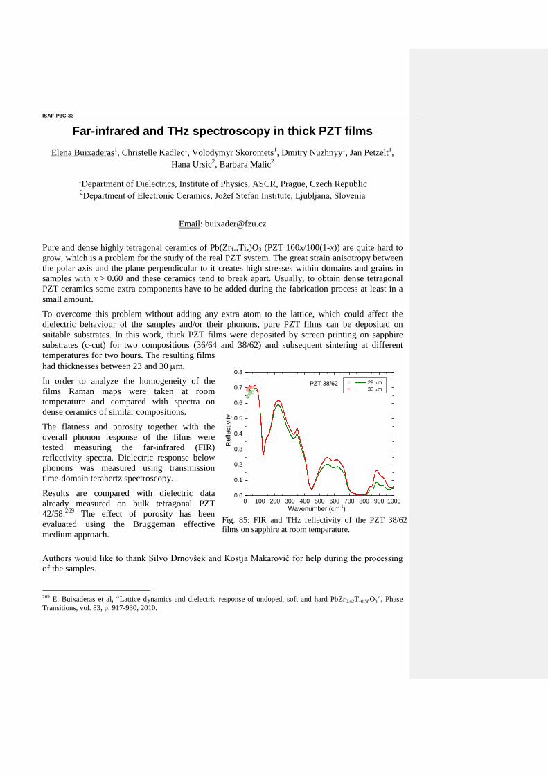
ISAF-P3C-33 ____________________________________________________________________________________________________________________
Far-infrared and THz spectroscopy in thick PZT films
Elena Buixaderas1, Christelle Kadlec
1, Volodymyr Skoromets
1, Dmitry Nuzhnyy
1, Jan Petzelt
1,
Hana Ursic2, Barbara Malic
2
1Department of Dielectrics, Institute of Physics, ASCR, Prague, Czech Republic
2Department of Electronic Ceramics, Jožef Stefan Institute, Ljubljana, Slovenia
Email: [email protected]
Pure and dense highly tetragonal ceramics of Pb(Zr1-xTix)O3 (PZT 100x/100(1-x)) are quite hard to
grow, which is a problem for the study of the real PZT system. The great strain anisotropy between
the polar axis and the plane perpendicular to it creates high stresses within domains and grains in
samples with x > 0.60 and these ceramics tend to break apart. Usually, to obtain dense tetragonal
PZT ceramics some extra components have to be added during the fabrication process at least in a
small amount.
To overcome this problem without adding any extra atom to the lattice, which could affect the
dielectric behaviour of the samples and/or their phonons, pure PZT films can be deposited on
suitable substrates. In this work, thick PZT films were deposited by screen printing on sapphire
substrates (c-cut) for two compositions (36/64 and 38/62) and subsequent sintering at different
temperatures for two hours. The resulting films
had thicknesses between 23 and 30 m.
In order to analyze the homogeneity of the
films Raman maps were taken at room
temperature and compared with spectra on
dense ceramics of similar compositions.
The flatness and porosity together with the
overall phonon response of the films were
tested measuring the far-infrared (FIR)
reflectivity spectra. Dielectric response below
phonons was measured using transmission
time-domain terahertz spectroscopy.
Results are compared with dielectric data
already measured on bulk tetragonal PZT
42/58.269
The effect of porosity has been
evaluated using the Bruggeman effective
medium approach.
Authors would like to thank Silvo Drnovšek and Kostja Makarovič for help during the processing
of the samples.
269
E. Buixaderas et al, “Lattice dynamics and dielectric response of undoped, soft and hard PbZr0.42Ti0.58O3”, Phase
Transitions, vol. 83, p. 917-930, 2010.
0 100 200 300 400 500 600 700 800 900 10000.0
0.1
0.2
0.3
0.4
0.5
0.6
0.7
0.8
Re
fle
ctivity
Wavenumber (cm-1)
29 m
30 mPZT 38/62
Fig. 85: FIR and THz reflectivity of the PZT 38/62
films on sapphire at room temperature.

ISAF-P3C-34 ____________________________________________________________________________________________________________________
Anisotropic electrical properties of BNT based textured lead-free piezoceramics
Haibo Zhang, Wook Jo, Jürgen Rödel
Institute of Materials Science, Technische Universität Darmstadt, 64287 Darmstadt, Germany
Lead-free piezoelectric materials have been the subject of ongoing experimental and
theoretical investigations due to their fundamental scientific interest and their importance in
technological applications. Various lead-free piezoceramics have been considered as candidates for
replacing Pb-based piezoceramics during the past decades. Bismuth sodium titanate,
(Bi1/2Na1/2)TiO3 (BNT), is considered to be an excellent candidate as a key lead-free piezoelectric
material, because it forms a solid solution with BaTiO3 (BT) or Bi1/2K1/2TiO3 (BKT) showing
improved dielectric and piezoelectric properties at the rhombohedral-tetragonal morphotropic phase
boundary (MPB). Recently, a giant strain of 0.45% was observed in BNT-BT-2KNN (with 2 mol%
KNN) ceramic at room temperature, which is higher than the strain of a commercial soft PZT
ceramic (PIC151, PI Ceramics). However, the giant strain can only be realized at very high electric
fields (>6 kV/mm), which should be reduced before it can be considered for industrial applications.
It is well known that physical properties of piezoelectric ceramics strongly depend on the
microstructure. Piezoelectric single crystals show enhanced performance as compared to
polycrystalline ceramics. As a consequence, textured piezoceramics are expected to possess
improved piezoelectric properties due to cooperating domains with uniformly aligned polarizations.
Most recently we found the poling field in textured BNT based piezoceramics is much lower than
that in random piezoceramics. In the present work, the BNT based piezoceramics were prepared by
the templated grain growth (TGG) technique. The processing route is to be improved to get highly
textured piezoceramics with various phase structures. The high degree of orientation (Lotgering
factor f > 90%) was achieved. The dielectric properties, ferroelectric properties and the bipolar and
unipolar strain of the textured piezoceramics were measured, analyzed and compared with those of
common bulk materials. Moreover, a special attention will be paid to the anisotropic electrical
properties using textured samples cut at different angles.
Reference:
1. Zhang, S. T., Kounga, A. B., Aulbach, E., Granzow, T., Jo, W., Kleebe, H. J., and Rödel, J. Lead-free piezoceramics with giant strain in the system Bi0.5Na0.5TiO3-BaTiO3-K0.5Na0.5NbO3 I. Structure and room
temperature properties. J. Appl. Phys., 2008, 103, 034107.
2. Seifert, K. T. P., Jo, W., and Rödel, J. Temperature-insensitive large strain of (Bi1/2Na1/2)TiO3-
(Bi1/2K1/2)TiO3-(K0.5Na0.5)NbO3 lead-free piezoceramics. J. Am. Ceram. Soc., 2010, 93, 1392-1396.
3. Jo, W., Dittmer, R., Acosta, M., Zang, J., Groh, C., Sapper, E., Wang, K., and Rödel, J. Giant electric-
field-induced strains in lead-free ceramics for actuator applications–status and perspective. J. Electroceram., 2012, 1-23.
ISAF-P3C-35 ____________________________________________________________________________________________________________________
The frequency and temperature dependence of hysteresis loop in P(VDF-TrFE) copolymer films
Manfang Mai1, Andreas Leschhorn
1, Herbert Kliem
1
1Institute of Electrical Engineering Physics, Saarland University, Saarbruecken, Germany
Email: [email protected]
The experimental hysteresis loop of ferroelectric poly(vinylidenefluoride-trifluoethylene) [P(VDF-
TrFE)] copolymer films is measured in a wide frequency and temperature range. For extrinsic
switching, ferroelectrics in general do not exhibit well-defined coercive fields. There are three
regions in the frequency dependence of coercive field. Below 1 Hz, the coercive field gets to a
saturation. In the lower frequency region from 1 Hz to 5 kHz, the hysteresis loop widens and the
coercive field increases with increasing frequency while the remanent polarization is almost
constant. As frequency increases, the excitation field changes faster than the dipole switching. The
dipoles become more difficult to catch up with the external signal and a higher coercive field is
expected. A linear fit of the frequency dependence of Ec in the log-log scale plot gives an exponent
value of 0.04. In the higher frequency region from 5 kHz to 1 MHz where the switching time is
longer than half of the external signal period, switching is suppressed and the amount of the
switchable polarization depends on the frequency. The hysteresis loop starts to shrink and the
coercive field decreases with increasing frequency. For a constant frequency, the hysteresis loop
measured at different temperature exhibits a linear decrease of coercive field with increasing
temperature. A double hysteresis loop is observed close to the Curie point and a sharp jump of the
remanent polarization is obtained in samples as thick as 600nm indicating a first order phase
transition. For samples as thin as 90nm, the double hysteresis loop of the polarization is absent and
the change of remanent polarization on temperature is smoother.
The above experimental results can be explained and simulated in the Weiss mean field model. It is
essentially a feedback model where the polarization evokes a field that in turn stimulates the
polarization. The model assumes that the electrostatic interaction between the dipoles leads to a
field αP proportional to the polarization of the system. The superposition of the external field and
the field due to the polarization yields the local field. At the dipole sites we find
loc aE E αP= + (1)
Assuming that the dipoles with dipole moment p and density n fluctuate thermally activated in
double well potentials, the transient polarization is described by a first-order differential equation (
relaxation time),
tanh( )loc
dP pτ P np E
dt kT+ = (2)
Combining (1) and (2) with Ea=E0sin(wt) the dynamic hysteresis loop can be obtained. To get the
double hysteresis loop, the piezoeffect in the ferroelectric is introduced to the model. Due to the
piezoeffect the volume V of the sample changes with the polarization ( piezo coefficient),
( )0 1V V νP= + (3)
This causes the dipole density, the dipole moment and/or the coupling constant varying with the
polarization. Eqns. (1)-(3) can yield a second order or first order phase transition depending on the
piezo coefficients of the system. The simulation results show good coincidence with the
experiments.
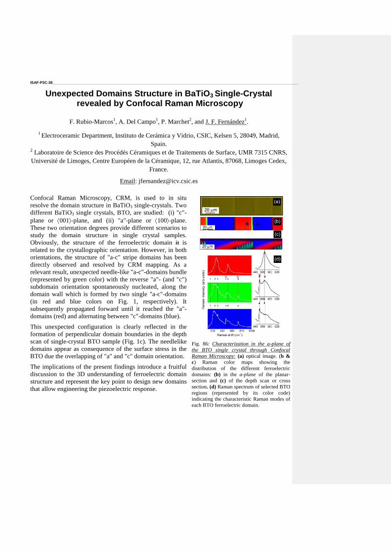
ISAF-P3C-36 ____________________________________________________________________________________________________________________
Unexpected Domains Structure in BaTiO3 Single-Crystal revealed by Confocal Raman Microscopy
F. Rubio-Marcos
1, A. Del Campo
1, P. Marchet
2, and J. F. Fernández
1.
1 Electroceramic Department, Instituto de Cerámica y Vidrio, CSIC, Kelsen 5, 28049, Madrid,
Spain. 2 Laboratoire de Science des Procédés Céramiques et de Traitements de Surface, UMR 7315 CNRS,
Université de Limoges, Centre Européen de la Céramique, 12, rue Atlantis, 87068, Limoges Cedex,
France.
Email: [email protected]
Confocal Raman Microscopy, CRM, is used to in situ
resolve the domain structure in BaTiO3 single-crystals. Two
different BaTiO3 single crystals, BTO, are studied: (i) "c"-
plane or 001-plane, and (ii) "a"-plane or 100-plane.
These two orientation degrees provide different scenarios to
study the domain structure in single crystal samples.
Obviously, the structure of the ferroelectric domain it is
related to the crystallographic orientation. However, in both
orientations, the structure of "a-c" stripe domains has been
directly observed and resolved by CRM mapping. As a
relevant result, unexpected needle-like "a-c"-domains bundle
(represented by green color) with the reverse "a"- (and "c")
subdomain orientation spontaneously nucleated, along the
domain wall which is formed by two single "a-c"-domains
(in red and blue colors on Fig. 1, respectively). It
subsequently propagated forward until it reached the "a"-
domains (red) and alternating between "c"-domains (blue).
This unexpected configuration is clearly reflected in the
formation of perpendicular domain boundaries in the depth
scan of single-crystal BTO sample (Fig. 1c). The needlelike
domains appear as consequence of the surface stress in the
BTO due the overlapping of "a" and "c" domain orientation.
The implications of the present findings introduce a fruitful
discussion to the 3D understanding of ferroelectric domain
structure and represent the key point to design new domains
that allow engineering the piezoelectric response.
Fig. 86: Characterization in the a-plane of
the BTO single crystal through Confocal
Raman Microscopy: (a) optical image. (b &
c) Raman color maps showing the
distribution of the different ferroelectric
domains: (b) in the a-plane of the planar-
section and (c) of the depth scan or cross
section. (d) Raman spectrum of selected BTO
regions (represented by its color code)
indicating the characteristic Raman modes of
each BTO ferroelectric domain.
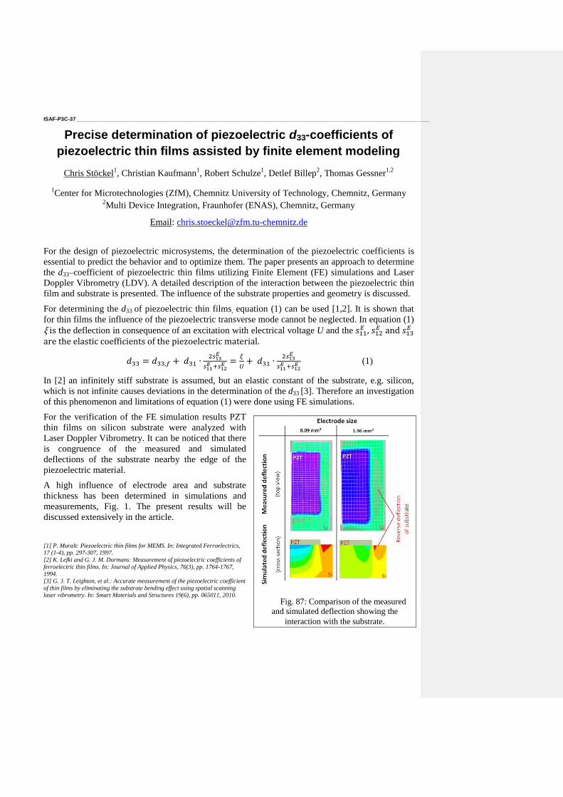
ISAF-P3C-37 ____________________________________________________________________________________________________________________
Precise determination of piezoelectric d33-coefficients of
piezoelectric thin films assisted by finite element modeling
Chris Stöckel1, Christian Kaufmann
1, Robert Schulze
1, Detlef Billep
2, Thomas Gessner
1,2
1Center for Microtechnologies (ZfM), Chemnitz University of Technology, Chemnitz, Germany
2Multi Device Integration, Fraunhofer (ENAS), Chemnitz, Germany
Email: [email protected]
For the design of piezoelectric microsystems, the determination of the piezoelectric coefficients is
essential to predict the behavior and to optimize them. The paper presents an approach to determine
the d33–coefficient of piezoelectric thin films utilizing Finite Element (FE) simulations and Laser
Doppler Vibrometry (LDV). A detailed description of the interaction between the piezoelectric thin
film and substrate is presented. The influence of the substrate properties and geometry is discussed.
For determining the d33 of piezoelectric thin films, equation (1) can be used [1,2]. It is shown that
for thin films the influence of the piezoelectric transverse mode cannot be neglected. In equation (1) ξ is the deflection in consequence of an excitation with electrical voltage U and the
, and
are the elastic coefficients of the piezoelectric material.
(1)
In [2] an infinitely stiff substrate is assumed, but an elastic constant of the substrate, e.g. silicon,
which is not infinite causes deviations in the determination of the d33 [3]. Therefore an investigation
of this phenomenon and limitations of equation (1) were done using FE simulations.
For the verification of the FE simulation results PZT
thin films on silicon substrate were analyzed with
Laser Doppler Vibrometry. It can be noticed that there
is congruence of the measured and simulated
deflections of the substrate nearby the edge of the
piezoelectric material.
A high influence of electrode area and substrate
thickness has been determined in simulations and
measurements, Fig. 1. The present results will be
discussed extensively in the article.
[1] P. Muralt: Piezoelectric thin films for MEMS. In: Integrated Ferroelectrics, 17 (1-4), pp. 297-307, 1997.
[2] K. Lefki and G. J. M. Dormans: Measurement of piezoelectric coefficients of
ferroelectric thin films. In: Journal of Applied Physics, 76(3), pp. 1764-1767, 1994.
[3] G. J. T. Leighton, et al.: Accurate measurement of the piezoelectric coefficient
of thin films by eliminating the substrate bending effect using spatial scanning laser vibrometry. In: Smart Materials and Structures 19(6), pp. 065011, 2010.
Fig. 87: Comparison of the measured
and simulated deflection showing the
interaction with the substrate.
ISAF-P3C-38 ____________________________________________________________________________________________________________________
Linear and Nonlinear Dielectric Properties of Ternary Solid
Solutions 0.4Na0.5Bi0.5TiO3-(0.6-x)SrTiO3-xPbTiO3
Šarūnas Svirskas1, Maksim Ivanov
1, Šarūnas Bagdzevičius
1, Jūras Banys
1, Jan Dec
2, Seweryn
Miga2, Marija Dunce
3, Eriks Birks
3, Maija Antonova
3, Andris Sternbergs
3
1Vilnius University, Faculty of physics, Saulėtekio av. 9, III b., LT-10222 Vilnius, Lithuania
2University of Silesia, Institute of Materials Science, Katowice, Poland
3Institute of Solid State Physics, University of Latvia, Kengaraga street 8, LV-1063 Riga, Latvia
Email: [email protected]
Sodium bismuth titanate (NBT) along with lead magnesium niobate (PMN) is one of the oldest
relaxor systems known. NBT attracts attention due to its promising electromechanical properties
and the absence of lead which is environmentally hazardous. Despite thorough studies which
already last for about 50 years there are still unanswered questions about this material. Recently, a
lot of interest in complex solid solutions containing NBT as primary material is shown270
. Such
materials as strontium titanate, lead titnate or barium titanate were mixed with sodium bismuth
titanate in order to enhance dielectric, piezoelectric properties or to get knowledge how A-site ions
influence phase transitions of NBT.
Temperature dependences of the linear and the first order and second order nonlinear dielectric
susceptibilities give useful information on the formation of polar nano-regions. On the other hand,
broadband linear dielectric spectroscopy allows to evaluate the dynamics of polar nano regions (or
dipolar entities in general). Distribution of relaxation times can be calculated from dielectric
spectra. On the other hand, nonlinear dielectric measurements help to identify the order of phase
transition precisely and the nonlinear scaling factor a3 shows the fundamental differences between
classical ferroelectrics and relaxors or dipolar glasses271
.
In this work we present our measurements of 0.4NBT-(0.6-x)ST-xPT (x = 0, 0.05, 0.1, 0.15, 0.2).
The exchange of strontium with lead changes dielectric properties dramatically. The system in low
lead side of phase diagram exhibits relaxor-like properties and when the content of PT increases the
phase transition from relaxor to ferroelectric state occurs.
270
Jung-Kun Lee et. al. J. Appl. Phys. 91, 4538 (2002) 271
Seweryn Miga, Jan Dec and Wolfgang Kleemann “Non-Linear Dielectric Response of Ferroelectrics, Relaxors and
Dipolar Glasses”, Ferroelectrics - Characterization and Modeling, ISBN: 978-953-307-455-9 (2011)
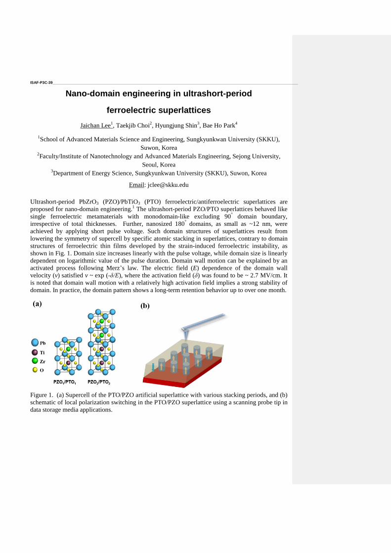
ISAF-P3C-39 ____________________________________________________________________________________________________________________
Nano-domain engineering in ultrashort-period
ferroelectric superlattices
Jaichan Lee1, Taekjib Choi
2, Hyungjung Shin
3, Bae Ho Park
4
1School of Advanced Materials Science and Engineering, Sungkyunkwan University (SKKU),
Suwon, Korea 2Faculty/Institute of Nanotechnology and Advanced Materials Engineering, Sejong University,
Seoul, Korea 3Department of Energy Science, Sungkyunkwan University (SKKU), Suwon, Korea
Email: [email protected]
Ultrashort-period PbZrO3 (PZO)/PbTiO3 (PTO) ferroelectric/antiferroelectric superlattices are
proposed for nano-domain engineering.1 The ultrashort-period PZO/PTO superlattices behaved like
single ferroelectric metamaterials with monodomain-like excluding 90° domain boundary,
irrespective of total thicknesses. Further, nanosized 180° domains, as small as ~12 nm, were
achieved by applying short pulse voltage. Such domain structures of superlattices result from
lowering the symmetry of supercell by specific atomic stacking in superlattices, contrary to domain
structures of ferroelectric thin films developed by the strain-induced ferroelectric instability, as
shown in Fig. 1. Domain size increases linearly with the pulse voltage, while domain size is linearly
dependent on logarithmic value of the pulse duration. Domain wall motion can be explained by an
activated process following Merz’s law. The electric field (E) dependence of the domain wall
velocity (v) satisfied v ~ exp (-δ/E), where the activation field (δ) was found to be ~ 2.7 MV/cm. It
is noted that domain wall motion with a relatively high activation field implies a strong stability of
domain. In practice, the domain pattern shows a long-term retention behavior up to over one month.
Figure 1. (a) Supercell of the PTO/PZO artificial superlattice with various stacking periods, and (b)
schematic of local polarization switching in the PTO/PZO superlattice using a scanning probe tip in
data storage media applications.

1. T. Choi, B.H. Park, H. Shin, and J. Lee, “Nano-domain engineering in ultra-short-period
ferroelectric superlattices”, Appl. Phys. Lett. 100, 222906, 2012.
ISAF-P3C-40 ____________________________________________________________________________________________________________________
Influence of spin-phonon coupling in SrMnO3 and CaMnO3 on
their dielectric properties and phonon spectra V. Goian
1, M. Savinov
1, V. Skoromets, J. Hejtmánek
1, V. Bovtun
1, M. Kempa
1, F. Borodavka
1, P.
Vaněk1, D. Nuzhnyy
1, A.A. Belik
2, J.H. Lee
3, K.M. Rabe
3, S. Kamba
1
1Institute of Physics, Academy of Sciences of the Czech Republic, Prague, Czech Republic
2 WPI-MANA, National Institute for Materials Science, Tsukuba, Ibaraki, Japan
3Department of Physics and Astronomy, Rutgers University, Piscataway, New Jersey, USA
Email: [email protected]
Investigated SrMnO3 and CaMnO3 ceramics crystallize in perovskite cubic Pm3m and
orthorhombic Pnma crystal structure, respectively and exhibit magnetic phase transition to
antiferromagnetic G-type phase near 230 K and 120 K, respectively. Although both materials are
paraelectric down to liquid He temperatures, recent first principles calculations predicted that both
systems can become ferroelectric and even ferromagnetic under a biaxial strain.272,273
The strain
effect was not yet confirmed experimentally, but Sakai et al.274
expanded SrMnO3 lattice by Ba
doping and successfully induced ferroelectricity in Sr1-xBaxMnO3 (x 0.45) with Tc 400 K and
canted ferromagnetism with TN 200 K. Important fact is that in this case the strong ferroelectricity
(PS = 13 C/cm2 ) is driven by displacement of magnetic Mn
4+ cations and the magnetoelectric
coupling is therefore the largest yet attained.274
Infrared reflectivity spectra of SrMnO3 ceramics reveal 25 cm-1
stiffening of the lowest-frequency
phonon below Néel temperature. The temperature change of polar phonon frequency is
extraordinarily high and we explain it by the exceptionally strong spin-phonon coupling. The same
phonon shift with temperature was obtained from the first principles calculations. Polar phonons
become Raman active below TN, although they are forbidden in the cubic crystal structure. It gives
evidence that the cubic symmetry is locally broken due to the strong magnetoelectric coupling.
Multiphonon and multimagnon scattering is also seen in Raman spectra. Microwave and THz
permittivity is strongly influenced by hopping electronic conductivity, which is caused by a small
non-stoichiometry of the sample. THz conductivity unusually increases on cooling, while the DC
conductivity markedly decreases. Thermoelectric measurements gave the room-temperature free
carriers concentration of ne = 3.16·1020
cm-3
and the sample composition was determined as
Sr2+
Mn4+
0.98Mn3+
0.02O2-
2.99.
Our radio-frequency dielectric, THz and infrared studies of CaMnO3 ceramics reveal metal
insulator phase transition at TN and splitting of some polar phonons below TN. Both effects give
evidence on the strong spin-phonon coupling, which reduces crystal symmetry in this material.
272
J.-H. Lee and K.M. Rabe, Epitaxial-strain-induced multiferroicity in SrMnO3 from first principles, Phys. Rev. Lett.
vol. 104, p. 207204, 2010. 273
S. Bhattacharjee, E. Bousquet, and P. Ghosez, Engineering multiferroism in CaMnO3, Phys. Rev. Lett. vol. 102, p.
117602, 2009 274
H. Sakai et al. Displacement-type ferroelectricity with off-center magnetic ions in perovskite Sr1-xBaxMnO3, Phys.
Rev. Lett. vol. 107, p. 137601, 2011
ISAF-P3C-41 ____________________________________________________________________________________________________________________
The nature of the defect structure of solid solutions based on lead
zirconate titanate (PZT) (by ESR and NMR method) I.P.Bykov
1, Yu.A. Zagorodniy
2, L.P.Yurchenko
1V. V.Trachevsky
3,
V.Dimza4, K.Nejezchleb
5, L.Jastrabik
6 A.Dejneka
6
1Frantcevych Institute for Problems of Materials Science, National academy of Sciences of Ukraine,
Kiev, 03680,Ukraine 2G.V. Kurdumov Institute for Metal Physics, National Academy of Sciences of Ukraine, Kiev
03680, Ukraine 3Technical Centre, National Academy of Sciences of Ukraine, 04070 Kiev,Ukraine
4Institute of Solid State Physics,University of Latvia, 226063Riga,Latvia
5Noliac Ceramics s.r.o.Školní 86, Libřice, CZ-503 44, Czech Republic
6Institute of Physics ASCR, v. v. i., 182 21 Prague, Czech Republic
The nature of intrinsic and impurity defects in lead zirconate titanate and lead (PZT, PLZT )
ceramics of various compositions prepared by solution chemistry has been explored. Using electron
paramagnetic resonance (EPR) and nuclear magnetic resonans (NMR), several defects sites have
been identified in the as-received materials, which include Fe3+
–oxygen vacancy (V 0) complex and
isolated Cu2+
ions. Both of these ions are incorporated into the lattice by replacing the Ti (Zr) ion. A
Fe3+
–VO complex serves as a sensitive probe of the local crystalline field environment of the
ceramic.The symmetry of this defects is roughly correlated with its phase diagram as the
composition PZT. The paramagnetic center Fe3+
–VO expariences tetragonal,rhombic and
ortorombic symmetry is varied PZT and PLZT. Paramagnetic center of the Cu2+
is differend, it
appears as though the addition of Zr and not a change in phase, is largely responsible in determining
the local environment of this acceptor impurity. The Cu2+
EPR weakly reflect the Ti-O or Zr-O
bond covalency in the perovskite lattice.
Two different lead ion positions with tetragonal and orthorhombic local symmetry were revealed in
PZT and PLZT ceramics on the base of 207
Pb NMR spectra measurements at room temperature. The
obtained data and their analysis on the base of the spectra shape calculations are in agreement
experiment. The comparison of observed spectra in PZT and PLZT with calculated spectra
allowing for resonance frequency chemical shift and spin-spin interaction show that the
displacements of lead and oxygen ions are not random quantities in the investigated PZT and
PLZT ceramic samples.
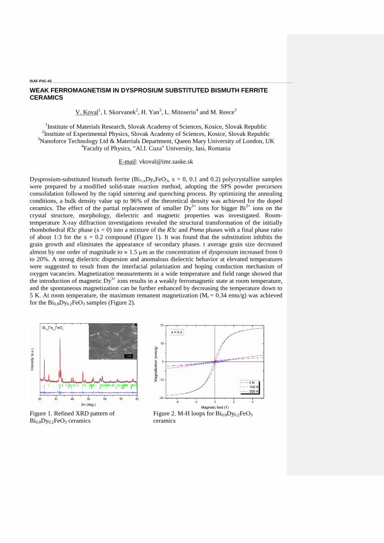
ISAF-P3C-42 ____________________________________________________________________________________________________________________
WEAK FERROMAGNETISM IN DYSPROSIUM SUBSTITUTED BISMUTH FERRITE CERAMICS
V. Koval1, I. Skorvanek
2, H. Yan
3, L. Mitoseriu
4 and M. Reece
3
1Institute of Materials Research, Slovak Academy of Sciences, Kosice, Slovak Republic
2Institute of Experimental Physics, Slovak Academy of Sciences, Kosice, Slovak Republic
3Nanoforce Technology Ltd & Materials Department, Queen Mary University of London, UK
4Faculty of Physics, "Al.I. Cuza" University, Iasi, Romania
E-mail: [email protected]
Dysprosium-substituted bismuth ferrite (Bi1-xDyxFeO3, x = 0, 0.1 and 0.2) polycrystalline samples
were prepared by a modified solid-state reaction method, adopting the SPS powder precursors
consolidation followed by the rapid sintering and quenching process. By optimizing the annealing
conditions, a bulk density value up to 96% of the theoretical density was achieved for the doped
ceramics. The effect of the partial replacement of smaller Dy3+
ions for bigger Bi3+
ions on the
crystal structure, morphology, dielectric and magnetic properties was investigated. Room-
temperature X-ray diffraction investigations revealed the structural transformation of the initially
rhombohedral R3c phase (x = 0) into a mixture of the R3c and Pnma phases with a final phase ratio
of about 1:3 for the x = 0.2 compound (Figure 1). It was found that the substitution inhibits the
grain growth and eliminates the appearance of secondary phases. t average grain size decreased
almost by one order of magnitude to 1.5 m as the concentration of dysprosium increased from 0
to 20%. A strong dielectric dispersion and anomalous dielectric behavior at elevated temperatures
were suggested to result from the interfacial polarization and hoping conduction mechanism of
oxygen vacancies. Magnetization measurements in a wide temperature and field range showed that
the introduction of magnetic Dy3+
ions results in a weakly ferromagnetic state at room temperature,
and the spontaneous magnetization can be further enhanced by decreasing the temperature down to
5 K. At room temperature, the maximum remanent magnetization (Mr = 0.34 emu/g) was achieved
for the Bi0.8Dy0.2FeO3 samples (Figure 2).
Figure 1. Refined XRD pattern of
Bi0.8Dy0.2FeO3 ceramics
Figure 2. M-H loops for Bi0.8Dy0.2FeO3
ceramics

ISAF-P3C-43 ____________________________________________________________________________________________________________________
Structure, dielectric, and piezoelectric properties of (0.95-x)
BiFeO3-x PbTiO3-0.05 Pb(Zn1/3Nb2/3)O3 ternary high Curie
temperature piezoelectric ceramics
Jiajia Jiang1, Jianguo Chen
1, Jinrong Cheng
1
1 Electronic Information Material Department, Material Institute, Shanghai, China
Email: [email protected]
A series of solid solutions (0.95-x) BiFeO3-x PbTiO3-0.05 Pb(Zn1/3Nb2/3)O3 (BF-PT-PZN) (x=
0.30, 0.31, 0.33, 0.35, 0.37, 0.40) have been fabricated by solid state reaction method. X-ray
diffraction analysis revealed that phase transition from rhombohedral to tetragonal was observed at
PT content of 0.35. Values of the dielectric constant εr, dielectric loss tangent tanθ, Curie
temperature Tc and piezoelectric constant d33 for the composition x=0.35 were of 250, 0.02, 550 °C
and 70 C/N, respectively. Temperature-dependent piezoelectric constant and electromechanical
coupling coefficient were stable from room temperature up to 450 oC, about 300
oC higher than that
of conventional Pb(Zr,Ti)O3 (PZT) piezoelectric ceramics. All these results together with the good
thermal stabilities made the BF-PT-PZN ceramics promising candidates for high temperature
piezoelectric applications.
Key words: High Curie Temperature, piezoelectric properties, ternary system
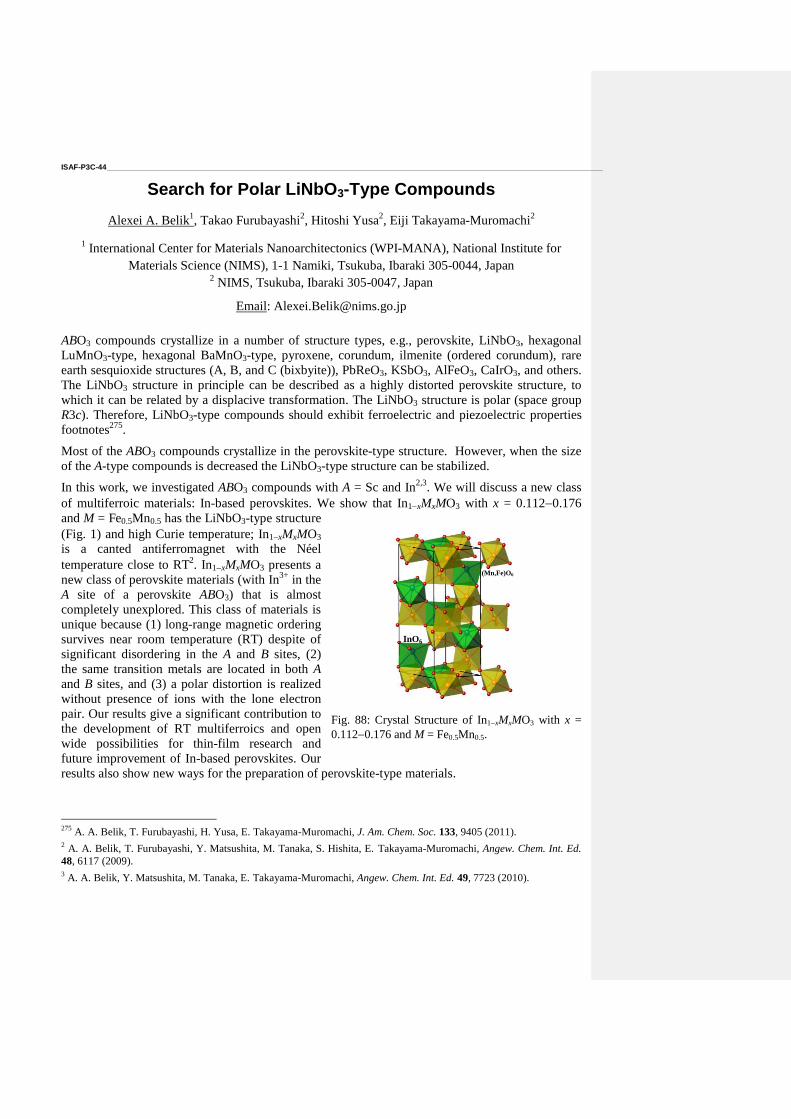
ISAF-P3C-44 ____________________________________________________________________________________________________________________
Search for Polar LiNbO3-Type Compounds
Alexei A. Belik1, Takao Furubayashi
2, Hitoshi Yusa
2, Eiji Takayama-Muromachi
2
1 International Center for Materials Nanoarchitectonics (WPI-MANA), National Institute for
Materials Science (NIMS), 1-1 Namiki, Tsukuba, Ibaraki 305-0044, Japan 2 NIMS, Tsukuba, Ibaraki 305-0047, Japan
Email: [email protected]
ABO3 compounds crystallize in a number of structure types, e.g., perovskite, LiNbO3, hexagonal
LuMnO3-type, hexagonal BaMnO3-type, pyroxene, corundum, ilmenite (ordered corundum), rare
earth sesquioxide structures (A, B, and C (bixbyite)), PbReO3, KSbO3, AlFeO3, CaIrO3, and others.
The LiNbO3 structure in principle can be described as a highly distorted perovskite structure, to
which it can be related by a displacive transformation. The LiNbO3 structure is polar (space group
R3c). Therefore, LiNbO3-type compounds should exhibit ferroelectric and piezoelectric properties
footnotes275
.
Most of the ABO3 compounds crystallize in the perovskite-type structure. However, when the size
of the A-type compounds is decreased the LiNbO3-type structure can be stabilized.
In this work, we investigated ABO3 compounds with A = Sc and In2,3
. We will discuss a new class
of multiferroic materials: In-based perovskites. We show that In1xMxMO3 with x = 0.1120.176
and M = Fe0.5Mn0.5 has the LiNbO3-type structure
(Fig. 1) and high Curie temperature; In1xMxMO3
is a canted antiferromagnet with the Néel
temperature close to RT2. In1xMxMO3 presents a
new class of perovskite materials (with In3+
in the
A site of a perovskite ABO3) that is almost
completely unexplored. This class of materials is
unique because (1) long-range magnetic ordering
survives near room temperature (RT) despite of
significant disordering in the A and B sites, (2)
the same transition metals are located in both A
and B sites, and (3) a polar distortion is realized
without presence of ions with the lone electron
pair. Our results give a significant contribution to
the development of RT multiferroics and open
wide possibilities for thin-film research and
future improvement of In-based perovskites. Our
results also show new ways for the preparation of perovskite-type materials.
275
A. A. Belik, T. Furubayashi, H. Yusa, E. Takayama-Muromachi, J. Am. Chem. Soc. 133, 9405 (2011). 2 A. A. Belik, T. Furubayashi, Y. Matsushita, M. Tanaka, S. Hishita, E. Takayama-Muromachi, Angew. Chem. Int. Ed.
48, 6117 (2009). 3 A. A. Belik, Y. Matsushita, M. Tanaka, E. Takayama-Muromachi, Angew. Chem. Int. Ed. 49, 7723 (2010).
(Mn,Fe)O6
InO6
Fig. 88: Crystal Structure of In1xMxMO3 with x =
0.1120.176 and M = Fe0.5Mn0.5.

ISAF-P3C-45 ____________________________________________________________________________________________________________________
Dielectric properties of modified BiFeO3 ceramics
Kachaporn Sanjoom1,3
, Duangpon Laksawat1, Kamonpan Pengpat
1,2, Sukum Eitssayeam
1,2 and
Gobwute Rujijanagul1,2,3,*
1Department of Physics and Materials science, Faculty of Science, Chiang Mai University,
Chiang Mai, 50200, Thailand 2Materials Science Research Center, Faculty of Science, Chiang Mai University, Chiang Mai,
50200, Thailand 3Thailand Center of Excellence in Physics, Commission on Higher Education, 328 Sri Ayutthaya
Road, Bangkok, 10400, Thailand
Email: [email protected]
The modified BiFeO3 (BFO) ceramics (BFO doped with Sb and Dy) were prepared by a solid-state
reaction method. Excess Bi2O3 (3 wt%) was introduced prior to powder calcination to compensate
for any Bi2O3 that may have been lost from the samples due to volatilization during heat treatments.
X-ray diffraction analysis revealed that pure phase perovskite was observed for the samples
calcined at a low heating rate. Dielectric behavior of undoped ceramic exhibited high dielectric
constant over a wide temperature region. However, the doping shifted this region to a higher
temperature. The doping affected the peak of dielectric loss of the samples. Activation energy of
dielectric relaxation also shifted with increasing the additive concentration. In addition, complex
impedance analysis was applied to determine the behavior of grain boundary and grain after doping.
Acknowledgements This work was supported by National Research University (NRU), Office of
Higher Education Commission (OHEC), Thailand center of excellence in Physics (Thep) and
Faculty of Science and Graduate School Chiang Mai University.
ISAF-P3C-46 ____________________________________________________________________________________________________________________
Electrical properties of PbLaZrTiOx capacitors
with conductive oxide buffer layer on Pt electrodes
Takeyasu Saito, Yoko Takada, Toru Tsuji, Naoki Okamoto, Kazuo Kondo, Takeshi Yoshimuraa,
Norifumi Fujimuraa, Koji Higuchi
b, Akira Kitajima
b, and Akihiro Oshima
b
Dept. of Chem. Eng., Osaka Prefecture University, Sakai, Osaka 599-8531, JAPAN a Dept. of Phys. Electro., Osaka Prefecture University, Sakai, Osaka 599-8531, JAPAN
b Inst. of Sci. and Ind. Res., Osaka University, Ibaraki, Osaka 567-0047, JAPAN
Email: [email protected]
Ferroelectric Random Access Memory (FeRAM) has attracted much attention and it is believed to be
next generation non-volatile memory for its high operation (read/write) speed and low power
consumption1). To achieve higher density integration, ferroelectric capacitors requires higher switching
charge and better fatigue and imprint properties. It was reported that the introduction of a buffer layer is
one of effective methods to improve fatigue characteristics of ferroelectric thin films2). A buffer layer
was also used to control the orientation of ferroelectric thin films3). In this study, we used conductive
Al-doped ZnO (AZO) and Sn doped In2O3 (ITO) as buffer layer on Pt bottom electrodes.
The substrates were highly (111)-oriented sputtered Pt as lower electrodes. PLZT
(Pb:La:Zr:Ti=113:3:30:70) films (500 nm) were prepared by the sol-gel method. The films were
deposited on Pt substrate by spin coating, at 3000 rpm for 20 s. Then, the gel-films were dried at 200℃
for 2 min in order to eliminate the solvent, and pyrolyzed at 300℃ for 10 min, in air for organic
components removal. The films were prepared by repeating (3 times) the deposition and pyrolysis
cycle. The prepared thickness was 500 nm. The coated films were finally calcined in air at 750℃, 10
min, in air for achieving crystallization. AZO buffer layers and top electrodes were deposited by PLD
(Pulsed Laser Deposition). This deposition was performed with a metal through mask having 50 um ~
500 um diameter. The composition of AZO and ITO targets were ZnO:Al2O3=98.5:1.5 wt.% and
In2O3:SnO2=95.0:5.0 wt.%, respectively.
Fig. 1 shows the polarization values of PLZT capacitors with
AZO top electrodes and with or without AZO buffer layer from 10
nm ~ 120 nm. Polarization value of PLZT capacitors with 10 nm
buffer layer and without buffer layer were 21.6 C/cm2 and 18.2
C/cm2, respectively at 15 V. The polarization ratio of PLZT
capacitors with 10 nm buffer layer and without buffer layer after107
10 V, 100 μs width and 1 ms interval cycles were 0.60 and 0.39,
respectively. PLZT capacitors with AZO buffer layer were also
confirmed to be promising in terms of hydrogen endurance.
References
1) M.M. Zhang et al, Solid-State Electronics, Vol. 53, p. 473
(2009).
2) H. Peng et al., Progress in Natural Science: Materials International, Vol. 22, p. 219 (2012)
3) X.S. Wang et al, Scripta Materialia, Vol. 46, p. 783 (2002)
Fig. 1 Hysteresis loops of PLZT
capacitors with or without buffer
layer.
ISAF-P3C-47 ____________________________________________________________________________________________________________________
Polarization Reversal in Crystals of Congruent Lithium
Tantalate at Elevated Temperatures
Chezganov Dmitry1, Shur Vladimir
1,2, Baturin Ivan
1,2, Akhmatkhanov Andrey
1,2
1Ferroelectric laboratory, Ural Federal University, Ekaterinburg, Russia
2Labfer Ltd., Ekaterinburg, Russia
Email: [email protected]
The polarization reversal and domain structure evolution under application of linear increasing field
has been studied in single crystalline congruent lithium tantalate (LiTaO3) in range from room
temperature to 250OC. The fitting of the switching current data by modification of Kolmogorov-
Avrami formula for switching in linear increasing field has been used for characterization
polarization reversal process276,277
. The static domain patterns revealed by selective chemical
etching have been visualized by optical microscopy at both polar surfaces.
The analysis of the switching current data obtained at low temperatures (below 200 O
C) allowed us
to separate the polarization reversal process in three stages. The first stage starting at low field was
fitted by β (2D) model corresponding to growth of domains existing in the initial state. The
beginning of appearance of new domains at the second stage allowed us to fit the current in terms of
(β+α) (2D) model. The termination of nucleation at the final stage leads to return to domain kinetics
according to β (2D) process.
The current shape changes essentially for the temperatures above 200OC. In this case the role of the
initial domain growth is negligible. Thus from the very beginning the switching current has been
fitted successively in terms of α (2D) model. The final stage of the switching process has been fitted
by exponential decay with additional switching current component corresponding to bulk
conductivity.
The proposed fitting allowed us to extract the value of the threshold field at which the nucleation of
new domains begins. The threshold field two times decrease was revealed in the studied
temperature range. The temperature dependence of the domain kinetics and shape of isolated
domains at both polar surfaces was observed. The shape of isolated domains changes from
triangular to circular at temperatures above 200OC. Moreover it was shown that the growth of non-
through domains observed at low temperatures changed by formation of through truncated conical
domains at elevated.
The observed experimental facts have been attributed to effective bulk screening due to increase of
the bulk conductivity at elevated temperatures.
The equipment of the UCSU “Modern Nanotechnology”, Institute of Natural Sciences, UrFU has
been used. The research was made possible in part by RFBR (Grants 13-02-01391-а, 11-02-91066-
CNRS-а), by Ministry of Education and Science (Сontract 14.513.12.0006), by OPTEC LLC.
276
V. Ya. Shur, E. L. Rumyantsev, S. D. Makarov, Kinetics of phase transformations in real finite systems: Application
to switching in ferroelectrics. J. Appl. Phys., vol. 84, p. 445–451, 1998.
277 V. Ya. Shur, E. L. Rumyantsev, S. D. Makarov, A. L. Subbotin, and V. V. Volegov, Transient current during
switching in increasing electric field as a basis for a new testing method. Integr. Ferroelectr., vol. 10, p. 223–230, 1995.

ISAF-P3C-48 ____________________________________________________________________________________________________________________
ELECTRICAL AND MAGNETIC PROPERTIES OF A NEW AURIVILLIUS PHASE
Bi14ThFe4Ti8O45
V. G. Vlasenkoa , V.A. Shuvaeva
a, S.Zubkov
a, S. Levchenkov
b
a Southern Federal University, Research Institute of Physics, Stachki Ave. 194, Rostov-on-Don,
344090, Russia
b Southern Federal University, Department of Chemistry, Zorge str. 7, Rostov-on-Don, 344090,
Russia
Recently Aurivillius phases, containing magnetic cations, such as Bi5Ti3FeO15, have drawn
special attention as they have potential to display both ferroelectric and ferromagnetic properties
simultaneously
A new layered perovskite-like oxide Bi14ThFe4Ti8O45, has been prepared, and the
temperature dependence of the dielectric and magnetic properties of the material has been
investigated. The composition and structure of the material is close to that of multiferroic material
Bi5Ti3FeO15 but it has a higher content of magnetoactive Fe3+
due to partial substitution of Bi by Th
in B perovskite positions. The dielectric properties of Bi14ThFe4Ti8O45 were studied in a
temperature range from 295 K to 1200 K at fixed frequencies of 100, 200, 500 and 1000 kHz. The
temperature dependence of the dielectric constant ε/ε0(Т) reveal a broad peak at about 970 K, which
is typical of a ferroelectric material with a high conductivity, undergoing a diffuse phase transition.
The magnetic susceptibility of the sample has been measured by the Faraday method in the
temperature range from 77.4 K to 300 K. The values of magnetic susceptibility of the sample at 295
and 77 K were found to be 5.88·10–6
и 14.16·10–6
cm3/g respectively and the corresponding
magnetic moments per formula unit were calculated to be 7.91 и 6.28 mB. The temperature
dependence of the 1/χg is typical for paramagnetic compounds with short range antiferromagnetic
exchange. The extrapolation of the part of the curve, measured at temperatures above 150 K, to the
low temperature region yields a Weiss constant of -200 K, which is lower than that of Bi5Ti3FeO15.
This shows that higher Fe concentration results in enhancing of antiferromagnetic coupling.
ISAF-P3C-49 ____________________________________________________________________________________________________________________
A New Criterion regarding the Flack parameter
J. Fábry1, M. Dušek
2
1 Department of Dielectrics, Institute of Physics AS CR, Prague, Czech Republic
2 Department of Structure Analysis, Institute of Physics AS CR, Prague, Czech Republic
Email: [email protected]
Existence of ferroelectric crystal structures is limited to the point groups 1, 2, 3, 4, 6, m, 2mm, 3m,
4mm, 6mm. All these point groups and the respective space groups are non-centrosymmetric. In
practice, non-centrosymmetric crystals structures, determined by single crystal X-ray diffraction,
are nowadays refined with inclusion of the Flack parameter278
. Flack and his collaborators
published a series of articles (e.g.279
) in which they investigated behaviour if this parameter and
assessment of its reliability in dependence of various conditions such as prominence of the resonant
scattering, presence of pseudocentrosymmetric substructure in the structure and quality of the
measurement. Here, another criterion for the reliability of the Flack parameter is suggested. It takes
into account the contribution of the resonant scattering to intensity of each diffraction hkl and
compares this contribution to the standard uncertainty of the observed intensity. The advantage of
these criteria follows from the fact they are independent of the measurement of the Bijvoet pairs.
278
H. D. Flack, Acta Cryst. A39, 876-881 (1983). 279
H. D. Flack & G. Bernardinelli, Acta Cryst. A64, 484-493 (2008).
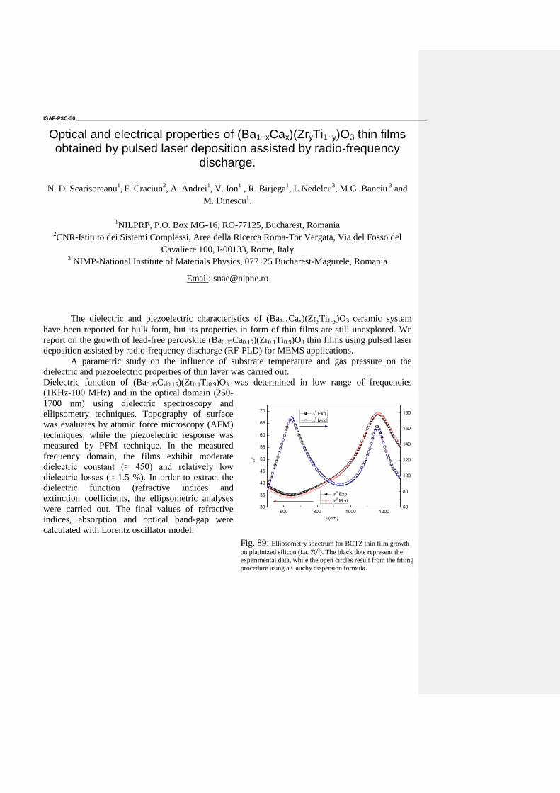
ISAF-P3C-50 ____________________________________________________________________________________________________________________
Optical and electrical properties of (Ba1−xCax)(ZryTi1−y)O3 thin films obtained by pulsed laser deposition assisted by radio-frequency
discharge.
N. D. Scarisoreanu1, F. Craciun
2, A. Andrei
1, V. Ion
1 , R. Birjega
1, L.Nedelcu
3, M.G. Banciu
3 and
M. Dinescu1.
1NILPRP, P.O. Box MG-16, RO-77125, Bucharest, Romania
2CNR-Istituto dei Sistemi Complessi, Area della Ricerca Roma-Tor Vergata, Via del Fosso del
Cavaliere 100, I-00133, Rome, Italy 3 NIMP-National Institute of Materials Physics, 077125 Bucharest-Magurele, Romania
Email: [email protected]
The dielectric and piezoelectric characteristics of (Ba1−xCax)(ZryTi1−y)O3 ceramic system
have been reported for bulk form, but its properties in form of thin films are still unexplored. We
report on the growth of lead-free perovskite (Ba0.85Ca0.15)(Zr0.1Ti0.9)O3 thin films using pulsed laser
deposition assisted by radio-frequency discharge (RF-PLD) for MEMS applications.
A parametric study on the influence of substrate temperature and gas pressure on the
dielectric and piezoelectric properties of thin layer was carried out.
Dielectric function of (Ba0.85Ca0.15)(Zr0.1Ti0.9)O3 was determined in low range of frequencies
(1KHz-100 MHz) and in the optical domain (250-
1700 nm) using dielectric spectroscopy and
ellipsometry techniques. Topography of surface
was evaluates by atomic force microscopy (AFM)
techniques, while the piezoelectric response was
measured by PFM technique. In the measured
frequency domain, the films exhibit moderate
dielectric constant (≈ 450) and relatively low
dielectric losses (≈ 1.5 %). In order to extract the
dielectric function (refractive indices and
extinction coefficients, the ellipsometric analyses
were carried out. The final values of refractive
indices, absorption and optical band-gap were
calculated with Lorentz oscillator model.
600 800 1000 120030
35
40
45
50
55
60
65
70
60
80
100
120
140
160
180
0
(nm)
0 Exp
0 Mod
0 Exp
0 Mod
Fig. 89: Ellipsometry spectrum for BCTZ thin film growth
on platinized silicon (i.a. 700). The black dots represent the
experimental data, while the open circles result from the fitting
procedure using a Cauchy dispersion formula.
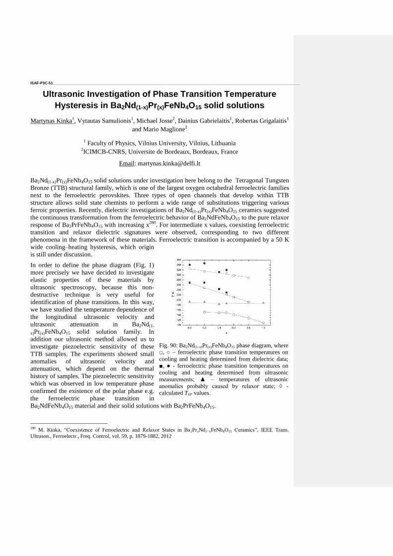
ISAF-P3C-51 ____________________________________________________________________________________________________________________
Ultrasonic Investigation of Phase Transition Temperature
Hysteresis in Ba2Nd(1-x)Pr(x)FeNb4O15 solid solutions
Martynas Kinka1, Vytautas Samulionis
1, Michael Josse
2, Dainius Gabrielaitis
1, Robertas Grigalaitis
1
and Mario Maglione2
1 Faculty of Physics, Vilnius University, Vilnius, Lithuania
2ICIMCB-CNRS, Universite de Bordeaux, Bordeaux, France
Email: [email protected]
Ba2Nd(1-x)Pr(x)FeNb4O15 solid solutions under investigation here belong to the Tetragonal Tungsten
Bronze (TTB) structural family, which is one of the largest oxygen octahedral ferroelectric families
next to the ferroelectric perovskites. Three types of open channels that develop within TTB
structure allows solid state chemists to perform a wide range of substitutions triggering various
ferroic properties. Recently, dielectric investigations of Ba2Nd(1-x)Pr(x)FeNb4O15 ceramics suggested
the continuous transformation from the ferroelectric behavior of Ba2NdFeNb4O15 to the pure relaxor
response of Ba2PrFeNb4O15 with increasing x280
. For intermediate x values, coexisting ferroelectric
transition and relaxor dielectric signatures were observed, corresponding to two different
phenomena in the framework of these materials. Ferroelectric transition is accompanied by a 50 K
wide cooling–heating hysteresis, which origin
is still under discussion.
In order to define the phase diagram (Fig. 1)
more precisely we have decided to investigate
elastic properties of these materials by
ultrasonic spectroscopy, because this non-
destructive technique is very useful for
identification of phase transitions. In this way,
we have studied the temperature dependence of
the longitudinal ultrasonic velocity and
ultrasonic attenuation in Ba2Nd(1-
x)Pr(x)FeNb4O15 solid solution family. In
addition our ultrasonic method allowed us to
investigate piezoelectric sensitivity of these
TTB samples. The experiments showed small
anomalies of ultrasonic velocity and
attenuation, which depend on the thermal
history of samples. The piezoelectric sensitivity
which was observed in low temperature phase
confirmed the existence of the polar phase e.g.
the ferroelectric phase transition in
Ba2NdFeNb4O15 material and their solid solutions with Ba2PrFeNb4O15.
280
M. Kinka, “Coexistence of Ferroelectric and Relaxor States in Ba2PrxNd1−xFeNb4O15 Ceramics”, IEEE Trans.
Ultrason., Ferroelectr., Freq. Control, vol. 59, p. 1879-1882, 2012
Fig. 90: Ba2Nd(1-x)Pr(x)FeNb4O15 phase diagram, where
□, ○ – ferroelectric phase transition temperatures on
cooling and heating determined from dielectric data;
■, ● - ferroelectric phase transition temperatures on
cooling and heating determined from ultrasonic
measurements; ▲ – temperatures of ultrasonic
anomalies probably caused by relaxor state; ◊ -
calculated TVF values.
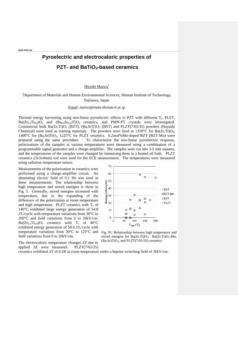
ISAF-P3C-52 ____________________________________________________________________________________________________________________
Pyroelectric and electrocaloric properties of
PZT- and BaTiO3-based ceramics
Hiroshi Maiwa1
1Department of Materials and Human Environmental Sciences, Shonan Institute of Technology,
Fujisawa, Japan
Email: [email protected]
Thermal energy harvesting using non-linear pyroelectric effects in PZT with different Tc, PLZT,
Ba(Zr0.2Ti0.8)O3 and (Ba0.8Sr0.2)TiO3 ceramics, and PMN-PT crystals were investigated.
Commercial bulk Ba(Zr,Ti)O3 (BZT), (Ba,Sr)TiO3 (BST) and PLZT(7/65/35) powders (Hayashi
Chemical) were used as starting materials. The powders were fired at 1350°C for Ba(Zr,Ti)O3,
1400°C for (Ba,Sr)TiO3, 1225°C for PLZT ceramics. 0.2mol%Mn-doped BZT (BZT-Mn) were
prepared using the same procedure. To characterize the non-linear pyroelectric response,
polarizations of the samples at various temperatures were measured using a combination of a
programmable signal generator and a charge-amplifier. The samples were cut into 3-5 mm squares,
and the temperatures of the samples were changed by immersing them in a heated oil bath. PLZT
ceramics (3x3x4mm) rod were used for the ECE measurement. The temperatures were measured
using radiation temperature sensor.
Measurements of the polarization in ceramics were
performed using a charge-amplifier circuit. An
alternating electric field of 0.1 Hz was used in
these measurements. The relationship between
high temperature and stored energies is show in
Fig. 5. Generally, stored energies increased with
temperature, due to the expanding of the
difference of the polarization at room temperature
and high temperature. PLZT ceramics with Tc of
140°C exhibited large energy generation of 54.8
J/L/cycle with temperature variations from 30°C to
200°C and field variations from 0 to 20kV/cm.
Ba(Zr0.2Ti0.8)O3 ceramics with Tc of 40°C
exhibited energy generation of 58.6 J/L/cycle with
temperature variations from 30°C to 125°C and
field variations from 0 to 20kV/cm.
The electrocaloric temperature changes ∆T due to
applied ∆E were measured. PLZT(7/65/35)
ceramics exhibited ∆T of 0.2K at room temperature under a bipolar switching field of 20kV/cm.
Fig. 91: Relationship between high temperature and
stored energies for Ba(Zr,Ti)O3, Ba(Zr,Ti)O3-Mn,
(Ba,Sr)TiO3, and PLZT(7/65/35) ceramics.

This study was supported in part by a grant in aid (C, No.22560671) and GRENE (Green network
of excellence) project from the ministry of education, culture, sports, science, and technology,
Japan.
ISAF-P3C-53 ____________________________________________________________________________________________________________________
Temperature Dependence of Electric Field Induced Changes in
Raman Spectrum of Lithium Niobate Single Crystals
Zelenovskiy Pavel1, Shur Vladimir
1, Mingaliev Eugene
1, Bourson Patrice
2, Fontana Marc
2
1Ferroelectric Laboratory, Ural Federal University, Ekaterinburg, Russia
2Laboratory of optical and photonic materials and systems, University of Lorraine, Metz, France
Email: [email protected]
The temperature dependence of Raman spectrum changes induced by residual depolarization field
in the vicinity of the domain walls has been studied in periodically poled lithium niobate single
crystals. It was demonstrated that the changes of measured integrated intensity and frequency shift
of specified Raman lines disappeared at temperatures above 120°C.
It has been shown experimentally that the parameters of specified Raman lines, being very sensitive
to lattice distortion, change remarkably in the vicinity of the domain walls produced at room
temperature in lithium niobate (LiNbO3, LN) single crystals281
. This effect is used for visualization
of the micro- and nanodomain structures in LN both at the surface and in the bulk using Raman
confocal microscopy282
. While the effect is absent for domain structure produced at elevated
temperatures. The changes of the Raman spectrum have been attributed to distortion of the crystal
lattice induced by the residual depolarization field existing in the vicinity of the domain walls near
the crystal surface1.
The changes of integrated intensity and frequency of E(TO8) and A1(LO4) Raman lines were
measured in ZxxZ )( configuration in the vicinity of neutral domain walls LN surface at different
steady-stated temperatures ranged from 25 to 120°C. The mapping of Raman spectra across the
domain walls has been done at constant temperature.
It has been revealed that the absolute values of the integrated intensity changes gradually decreased
with temperature increasing and disappeared at 120°C. Frequency shift of E(TO8) line possesses
strong variations while the shift of A1(LO4) line remains approximately constant during the whole
temperature range. At temperature 120°C frequency shift rapidly goes to zero for both spectral
lines.
The additional experimental measurement of the temperature dependence of the pyroelectric field
during heating with the constant rate about 7°C/min demonstrates the field maximum just at 120°C.
This fact has been attributed to increase of the bulk conductivity leading to more effective screening
of the depolarization field and decreasing of pyroelectric field283
. It is clear that effective bulk
screening at elevated temperature must diminish the residual depolarization field in the vicinity of
the domain wall thus leading to disappearance of the changes of Raman spectrum.
The research was made possible in part by RFBR (Grants 13-02-01391-а, 12-02-31377-mol-a, 11-
02-91066-CNRS-а); by Ministry of Education and Science (Contracts 14.513.12.0006 and
281
P.S. Zelenovskiy, V.Y. Shur, P. Bourson, M.D. Fontana, D.K. Kuznetsov, and E.A. Mingaliev, Ferroelectrics 398, 34 (2010). 282
P.S. Zelenovskiy, M.D. Fontana, V.Ya. Shur, P. Bourson, and D.K. Kuznetsov, Appl. Phys. A 99, 741 (2010). 283
V.Ya. Shur, D.K. Kuznetsov, E A. Mingaliev et al., Appl. Phys. Lett. 99, 082901 (2011).

16.740.11.0585), by OPTEC LLC and in terms of Ural Federal University development program
with the financial support of young scientists.
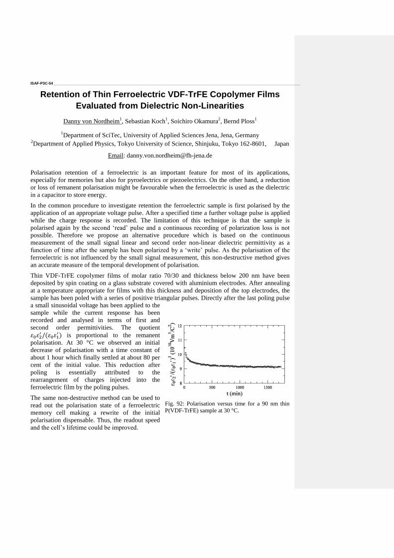
ISAF-P3C-54 ____________________________________________________________________________________________________________________
Retention of Thin Ferroelectric VDF-TrFE Copolymer Films
Evaluated from Dielectric Non-Linearities
Danny von Nordheim1, Sebastian Koch
1, Soichiro Okamura
2, Bernd Ploss
1
1Department of SciTec, University of Applied Sciences Jena, Jena, Germany
2Department of Applied Physics, Tokyo University of Science, Shinjuku, Tokyo 162-8601, Japan
Email: [email protected]
Polarisation retention of a ferroelectric is an important feature for most of its applications,
especially for memories but also for pyroelectrics or piezoelectrics. On the other hand, a reduction
or loss of remanent polarisation might be favourable when the ferroelectric is used as the dielectric
in a capacitor to store energy.
In the common procedure to investigate retention the ferroelectric sample is first polarised by the
application of an appropriate voltage pulse. After a specified time a further voltage pulse is applied
while the charge response is recorded. The limitation of this technique is that the sample is
polarised again by the second ‘read’ pulse and a continuous recording of polarization loss is not
possible. Therefore we propose an alternative procedure which is based on the continuous
measurement of the small signal linear and second order non-linear dielectric permittivity as a
function of time after the sample has been polarized by a ‘write’ pulse. As the polarisation of the
ferroelectric is not influenced by the small signal measurement, this non-destructive method gives
an accurate measure of the temporal development of polarisation.
Thin VDF-TrFE copolymer films of molar ratio 70/30 and thickness below 200 nm have been
deposited by spin coating on a glass substrate covered with aluminium electrodes. After annealing
at a temperature appropriate for films with this thickness and deposition of the top electrodes, the
sample has been poled with a series of positive triangular pulses. Directly after the last poling pulse
a small sinusoidal voltage has been applied to the
sample while the current response has been
recorded and analysed in terms of first and
second order permittivities. The quotient
(
) is proportional to the remanent
polarisation. At 30 °C we observed an initial
decrease of polarisation with a time constant of
about 1 hour which finally settled at about 80 per
cent of the initial value. This reduction after
poling is essentially attributed to the
rearrangement of charges injected into the
ferroelectric film by the poling pulses.
The same non-destructive method can be used to
read out the polarisation state of a ferroelectric
memory cell making a rewrite of the initial
polarisation dispensable. Thus, the readout speed
and the cell’s lifetime could be improved.
Fig. 92: Polarisation versus time for a 90 nm thin
P(VDF-TrFE) sample at 30 °C.

ISAF-P3C-55 ____________________________________________________________________________________________________________________
Composition and Morphology Effects on the Thermal
Conductivity of PZT Thin Films
Jon F. Ihlefeld,1 Brian M. Foley,
2 John C. Duda,
2 Harlan Brown-Shaklee,
1 Douglas Medlin,
3 Bryan
D. Huey,4 Bonnie B. McKenzie,
1 Brady J. Gibbons
5 and Patrick E. Hopkins
2
1Sandia National Laboratories, Albuquerque, New Mexico/USA
2Department of Mechanical and Aerospace Engineering, University of Virginia, Charlottesville,
Virginia/USA 3Sandia National Laboratories, Livermore, California/USA
4Institute of Materials Science, University of Connecticut, Storrs, Connecticut/USA
5Materials Science, School of Mechanical, Industrial, and Manufacturing Engineering, Corvallis,
Oregon/USA
Email: [email protected]
In this presentation we explore the effects of composition, phase, and morphology on the thermal
conductivity of lead zirconate titanate thin films. Epitaxial and polycrystalline films with
compositions ranging from PbZr0..2Ti0.8O3 to PbZr0..8Ti0.2O3 have been prepared by chemical
solution deposition on (001)-oriented SrTiO3 and Pt/ZnO/SiO2/Si substrates. Thermal
conductivities were measured using time-domain thermoreflectance at room temperature. For
single-crystalline films, the composition dependent thermal conductivity trend will be shown to be
consistent with that expected for alloy scattering from the mixed B-site. For polycrystalline films, it
will be shown that grain boundary scattering dominates the measured thermal conductivities and
decreases the composition dependence. For specific compositions in both epitaxial and
polycrystalline films, however, a decreased thermal conductivity is observed that is consistent with
scattering from finer-scale features. These results will be discussed in the context of phonon
scattering from domain walls. This presentation represents one of the first studies of the
composition and morphology dependence of thermal conductivity in a ferroelectric thin film.
Sandia National Laboratories is a multi-program laboratory managed and operated by Sandia
Corporation, a wholly owned subsidiary of Lockheed Martin Corporation, for the U.S. Department
of Energy's National Nuclear Security Administration under contract DE-AC04-94AL85000.

ISAF-P3C-56 ____________________________________________________________________________________________________________________
Comparable Measurements and Modeling of Piezoelectric Thin
Films for MEMS application
Thorsten Schmitz-Kempen1, Stephan Tiedke
1, Peter Mardilovich
2, Subramanian Sivaramakrishnan
2,
Thomas Lisec3, Fabian Stoppel
3
1aixACCT Systems GmbH, Aachen, Germany
2Hewlett-Packard, Corvallis, USA
3Fraunhofer Institute for Silicon Technology, Itzehoe, Germany
Email: [email protected]
Accurate and reliable measurements of piezoelectric coefficients on thin films are required to
perform thin film process development and compare different manufacturing techniques and quality
especially in MEMS applications.
State of the art measurements are performed by double-beam laser interferometry since many years,
however the variety of parameter ranges and test conditions make it difficult to compare
measurement results. Films on a substrate exhibit effective piezoelectric coefficients due to
substrate clamping and the coefficient also depends on feature size and substrate thickness. This
was shown by FEM simulations for the case of d33,f measurements by DBLI (K. Prume et al, Proc.
IEEE ISAF 2004) and latest simulation and measurement results show that a considerable reduction
of the measured d33,f was obtained for small electrodes and an increase for large electrodes. The
measured d33,f value at large electrodes is even larger than the true d33,f of the film and for small
feature sizes it is lower. A feature size chosen equivalent to the substrate thickness exhibits the most
exact number for the effective coefficient d33,f (S. Sivaramakrishnan et al, presentation on 3rd
PiezoMEMS Workshop 2013).
Furthermore nonlinearity and hysteresis of ferroelectric films requires the definition of
measurement parameters to obtain comparable procedures regarding hysteresis, poling conditions,
and other property nonlinearities, voltage and frequency dependency of coefficients, and large and
small signal responses. For easier comparison of films a large signal coefficient (d33,ls) is introduced
as the average slope of a displacement vs. voltage measurement over the full operating voltage
range. For thin film measurements it reflects the potential displacement in typical actuator
applications in comparison to small-signal coefficients and allows better comparison of materials
for actuation.
ISAF-P3C-57 ____________________________________________________________________________________________________________________
Investigation of the dielectric, piezoelectric and elastic
properties of BaTiO3 by means the thermal noise method
I. Shnaidshtein1, P. Bednyakov
2, B. Strukov
1
1Lomonosov Moscow State University, Moscow, Russia
2École Polytechnique Fédérale de Lausanne, Lausanne, Suisse
Email: [email protected]
Crystals of barium titanate BaTiO3 (BT) belong to classical model ferroelectrics which have been
extensively investigated by various methods since the discovery of their ferroelectric properties.
However the role of the fluctuation effects at the ferroelectric phase transition in BT crystals is so
far not clear284
. This is due both to the fact that the ferroelectric phase transition in BT is a phase
transition of the first order and with the difficulty to differ the behavior related with the fluctuations
and other similar factors such as defects or the experiment conditions.
The thermal noise method allows to controlling the experimental conditions due to the absence of
the measuring voltage. Moreover, that in BT crystals noise voltage level is high and as it was shown
earlier by Brophy and Webb285
it can be changed by changing the thermal conditions of the
experiment. By this way we can separate the different contributions responsible for the noise
voltage, such as thermal Barkhausen noise, white noise and the noise caused by the piezoelectric
effect.
This approach has been used in our previous work286
. In addition to the results obtained there, we
discuss new data on the impact of the bias electric field for different types of noise near the
ferroelectric phase transition. These data are directly related to the observation of the piezoelectric
effect in the cubic phase of BT crystals. Also for the first time the possibility of determining of the
elastic properties of the crystal by the noise measurements are discussed.
This work is supported by Russian Foundation for Basic Research (project of №11-02-01317).
284
Y.L. Wang, A.K. Tagantsev, D. Damjanovic, N. Setter, V.K. Yarmarkin, A.I. Sokolov, Anharmonicity of BaTiO3
single crystals, Phys. Rev B, vol. 73, 132103, 2006. 285
J.J Brophy, S.L. Webb, Critical fluctuation in triglecene sulphate, Phys. Rev, vol. 128, 584, 1962. 286
P.S. Bednyakov, I.V. Shnaidshtein, B.A. Strukov, Investigation of the dielectric properties of BaTiO3 single crystals
of different qualities by the thermal noise method, Physics of the Solid State, vol. 53, 350, 2011.

ISAF-P3C-58 ____________________________________________________________________________________________________________________
Band gap asymmetry and local segregation in barium
zirconate titanate epitaxial thin films
Jofre Ventura1, Sergio Hernández
2, Adolf Canilas
1, Jordi Sancho-Parramón
3, Luis Emerson Coy
1,
Cèsar Ferrater1, María del Carmen Polo
1, María Victoria García-Cuenca
1, Manuel Varela
1
1Department de Física Aplicada I Òptica, Universitat de Barcelona, Barcelona, Spain
2Department d’Electrònica, Universitat de Barcelona, Barcelona, Spain
3 Ruđer Bošković Institute, Bijenička 54, Zagreb 10000, Croatia
Email: [email protected]
The substitution of Ti4+
by Zr4+
in BaZrxTi1-xO3 (BZT) changes its dielectric character from proper
ferroelectric to ferroelectric with pinched phase transition, second-order-like diffuse phase
transition, relaxor behavior, polar cluster and then simple paraelectric287
. The dynamic coupling
between BaTiO3 polar nanoregions and BaZrO3 nonpolar ones is thought to be the mechanism
behind such a rich phase diagram. However, these short-range composition variations are not
detectable with X-ray diffraction, which relies on the coherent scattering from many unit cells, and
this topic is thus rarely addressed.
We have grown thin films of BZT on (001)-oriented
Nb:SrTiO3 substrates by pulsed laser deposition.
Structural characterization by X-ray diffractometry
showed that a solid solution with single cube-on-
cube epitaxial domain is formed across the entire
compositional range. Excluding tetragonal BaTiO3,
the unit cell of BZT is cubic and its volume increases
linearly with Zr content, suggesting proper
intermixing of Zr and Ti into an average BZT lattice.
However, two-mode behavior of the A1g breathing
mode of the oxygen octahedron was detected in the
Raman inelastic scattering spectra of BZT, which
might be attributed to a heterogeneous distribution of
B-site cations with different Ti-O and Zr-O bond
distances (or local clustering) rather than long-range
ordering288
.
Furthermore, the dependence of band gap energy
with composition determined from spectroscopic ellipsometry measurements (Fig. 1) does not
follow a bowing parabolic dependence as one could expect from local lattice relaxations alone.
Instead, an asymmetric trend suggests the tendency to the enrichment of one chemical species over
another, as expected from a nonideal solid solution behavior289
. An empirical modified Vegard’s
equation with an asymmetry weighted function was successfully fitted to the experimental data.
287
T. Maiti et al., J.Am. Ceram.Soc., vol. 91, p. 1769,-1780, 2008. 288
I. Levin et al., Chem. Mater., vol. 18, p. 854-860, 2006. 289
S. Lee et al., J. Appl. Phys., vol. 107, p. 023523, 2010.
0,0 0,2 0,4 0,6 0,8 1,0
3,0
3,2
3,4
3,6
3,8
4,0
4,2
Bandgap E
nerg
y E
g (
eV
)
x in BaZrxTi
1-xO
3
Fig. 93: Dependence of band gap energy on Zr
content as obtained from spectroscopic
ellipsometry (black points) and assymetric
empirical model (orange line).

ISAF-P3C-59 ____________________________________________________________________________________________________________________
Determination of the vibrational properties of potassium
titanyl phosphate and identification of domain structure
sensitive phonon modes
M. Rüsing1, C. Buchholz
1, G. Berth
1,2 and A. Zrenner
1,2
1Department Physik, Universität Paderborn, 33098 Paderborn, Germany
2Center for Optoelectronics and Photonics Paderborn (CeOPP), 33098 Paderborn, Germany
Email: [email protected]
Ferroelectric materials are commonly used for a wide range of applications in the field of integrated
optics. Their special characteristics such as permanent polarization and nonlinear properties make
them an ideal material for nonlinear devices. Especially the opportunity for quasi- phase-matching
via periodically poled structures is a central topic for the application of this material class. One of
these ferroelectrics is potassium titanyl phosphate (KTP) which has attracted particular attention
due to its large electro-optical coefficients, high nonlinear coefficients and high damage
threshold290
. For advancement in application of periodically poled devices often smaller periods of
alternating domains with opposing polarity are needed. In previous work it has been shown, that
second harmonic generation can be used for imaging of ferroelectric domain walls in KTP291
. Due
to complex domain engineering a deep understanding of the material properties is inevitable. Here
Raman spectroscopy represents a widely used method for elemental analysis of crystal structures.
In this work confocal Raman spectroscopy was applied on KTP. The confocal application enriches
Raman spectroscopy with the power of high spatial resolution enabling the characterization of the
transferred ferroelectric domain structure. With this combined technology a detailed analysis of
additional information becomes possible. Raman spectroscopy has already been successfully used
to examine the ferroelectric domain structure in other ferroelectric materials292
.
Confocal Raman spectroscopy was applied for studying the vibrational properties of KTP in its
entirety. Therefore polarization-dependent measurements in various scattering configurations were
performed. Our measurements are in good agreement with previous work on KTP293
. Furthermore
we have characterized periodically poled potassium titanyl phosphate in terms of polarity- and
structure-sensitive phonon modes. Here we found vibrations which are linked to the ferroelectric
domain structure. This might be due to changes in the polarizability originated from both the
domain boundaries and the inner field distribution. Hence a direct visualization based on the spatial
Raman intensity variation of specific phonon modes becomes possible.
290
M. E. Hagerman, K. R. Poeppelmeier, “Review of the Structure and Processing-Defect-Property Relationships of
Potassium Titanyl Phosphate: A Strategy for Novel Thin-Film Photonic Devices”, Chem. Mater., vol. 7, p. 602-621,
1995. 291
S. I. Bozhevlnyi et al., “Second-harmonic imaging of ferroelectric domain walls”, Appl. Phys. Lett., vol. 73, p. 1814-
1817, 1998. 292
G. Berth et al., “Imaging of the Ferroelectric Domain Structures by Confocal Raman Spectroscopy”, Ferroelectrics.,
vol. 420, p. 44-48, 2011. 293
G. E. Kugel et. al., “The vibrational spectrum of KTiOPO4 single crystal studied by Raman and infrared reflectivity
spectroscopy”, J. Phys C: Solid State Phys., Vol. 21, p. 5565-5583, 1988.

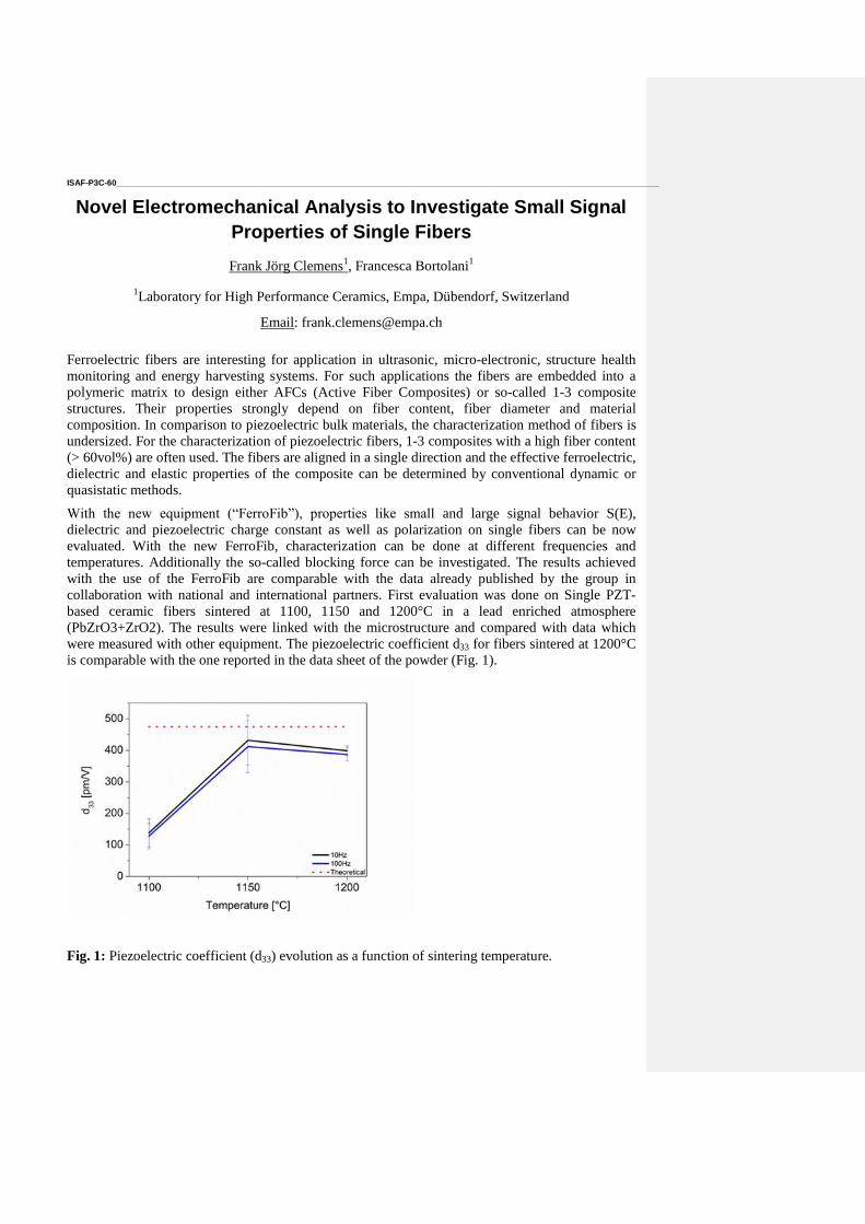
ISAF-P3C-60 ____________________________________________________________________________________________________________________
Novel Electromechanical Analysis to Investigate Small Signal
Properties of Single Fibers
Frank Jörg Clemens1, Francesca Bortolani
1
1Laboratory for High Performance Ceramics, Empa, Dübendorf, Switzerland
Email: [email protected]
Ferroelectric fibers are interesting for application in ultrasonic, micro-electronic, structure health
monitoring and energy harvesting systems. For such applications the fibers are embedded into a
polymeric matrix to design either AFCs (Active Fiber Composites) or so-called 1-3 composite
structures. Their properties strongly depend on fiber content, fiber diameter and material
composition. In comparison to piezoelectric bulk materials, the characterization method of fibers is
undersized. For the characterization of piezoelectric fibers, 1-3 composites with a high fiber content
(> 60vol%) are often used. The fibers are aligned in a single direction and the effective ferroelectric,
dielectric and elastic properties of the composite can be determined by conventional dynamic or
quasistatic methods.
With the new equipment (“FerroFib”), properties like small and large signal behavior S(E),
dielectric and piezoelectric charge constant as well as polarization on single fibers can be now
evaluated. With the new FerroFib, characterization can be done at different frequencies and
temperatures. Additionally the so-called blocking force can be investigated. The results achieved
with the use of the FerroFib are comparable with the data already published by the group in
collaboration with national and international partners. First evaluation was done on Single PZT-
based ceramic fibers sintered at 1100, 1150 and 1200°C in a lead enriched atmosphere
(PbZrO3+ZrO2). The results were linked with the microstructure and compared with data which
were measured with other equipment. The piezoelectric coefficient d33 for fibers sintered at 1200°C
is comparable with the one reported in the data sheet of the powder (Fig. 1).
Fig. 1: Piezoelectric coefficient (d33) evolution as a function of sintering temperature.
ISAF-P3C-61 ____________________________________________________________________________________________________________________
Magnetoelectric coupling in Bi1-xAxFeO3 (A=La, Nd) solid solutions
A.A. Amirov 1, I.K. Kamilov
1, L.A. Reznichenko
2, O.N. Razumovskaya
2, I.A. Verbenko
2
1 Institute of Physics, Dagestan Scientific Center of Russian Academy of Sciences, 94 Yaragskogo
Street, Makhachkala, Russia 2 Institutes of Physics, South Federal University, 194 Stachki Street, Russia
e-mail: [email protected]
The investigation of systems with strongly coupled magnetic and electronic degrees of freedom has
drawn significant interest in recent years due to both challenges for many-body theory as well as for
potential technical applications [1–2]. In connection with the compounds on base of BiFeO3 are
very perspective multiferroic materials due to high temperature of magnetic and ferroelectric phase
transitions, bad conductivity and simple chemical structure [1-2].
High quality ceramics were synthesized on the basic of Bi1-xAxFeO3 (A=La, Nd; x=0-0.2) solid
solutions. Their crystal and grain structure, Mossbauer spectra, dielectric, magnetic, thermal
characteristics were studied. The ac-susceptibility vs. temperature curve of BiFeO3 has a sharp peak
at 646 K which corresponds to the antiferromagnetic phase transition and it is confirmed by
literature data [3]. The anomalies of dielectric permeability, spacing parameter, thermal
conductivity and heat capacity near temperature of antiferromagnetic order TN were observed in all
samples and it is related with correlation between magnetic and ferroelectric subsystem which is
typical for multiferroics. The magnetization curves also have been studied at the room temperature
for the samples. The magnetization of pure BiFeO3 is small and grows linearly with magnetic field.
Such type of magnetization curve is typical for antiferromagnetic materials. La and Nd substitutions
lead to increase magnetic properties of BiFeO3. The substitution Bi by La or Nd changes the
temperature of the antiferromagnetic order and increases the magnetization of pure BiFeO3. The
magnetic properties change occurs not only on account of magnetic moment and ionic radiuses
(lanthanum atom has no its magnetic moment), but also because of La and Nd ions magnetic
moments anisotropy.
The samples were also studied for the presence of the magnetodielectric effect
(magnetocapacitance), which is a change in the permittivity of the sample caused by the application
of a magnetic field
,
where ε(H) and ε(0) are the permittivities in a magnetic field and in the absence of it, respectively.
The measurement results showed an increase in magnetodielectric effect is associated with an
increase in the degree of interaction between the dipole and magnetic subsystems. The slower
increase of magnetocapacitance in the range 0.05 ≤ x ≤ 0.1 associated with the change of
predominant mechanism in the solid solutions, as in 0.15 ≤ x ≤ 0.2 - with the existence of invar
effect due to the appearence of a new monoclinic phase. 1J. Wang et al., Science 299, 1719 (2003)
2A.K. Zvezdin and A.P. Pyatakov, Sov. Phys. Usp. 47, 8 (2004).
3Sosnowska and A. K. Zvezdin, J. Magn. Magn. Mater 140–44, 167 (1995)
ISAF-P3C-62 ____________________________________________________________________________________________________________________
Measurement of Vibration Mode Structure for Adaptive
Vibration Suppression System by Digital Holography
Pavel Psota1,2
, Vít Lédl1,2
, Roman Doleček1,2
, Pavel Mokrý1,2
1TOPTEC Centre, Turnov, Czech Republic
2Technical University of Liberec, Liberec, Czech Republic
Email: [email protected]
The frequency-shifted digital holographic interferometry (FSDHI) for measurements of vibration
amplitudes in the range of nanometers has been recently introduced and demonstrated294,295
. The
FSDHI method addressed some of the drawbacks of conventional methods and was mainly used for
measurements of piezoelectric transformer vibration amplitudes and mode structures296
. The
limiting factor for the application of this method is the maximal measured value of the vibration
amplitude without the risk of an ambiguity. The value is approximately 80nm for the frequency
doubled Nd: YAG line.
Since FSDHI enables us to precisely measure vibration amplitudes over the whole inspected area
with a very high lateral resolution, it could also be a very useful tool for measurements of vibration
amplitudes and mode structures in the research and development of adaptive noise suppression
systems. Such measurements would provide a necessary feedback about the system behavior.
The aforementioned issues have motivated the work where we put an effort to the modification of
the FSDHI method with the aim of increasing its dynamic range while keeping its precision. The
essential breakthrough in this paper is an innovative data processing technique based on recurrence
relationship of the first kind Bessel functions. Finally, a measurement method called high dynamic
range - frequency shifted digital holographic interferometry (HDR-FSDHI) was developed. The
method has the ability to measure in a nearly arbitrary range of vibration amplitudes.
The HDR-FSDHI method was applied on a vibration amplitudes measurement of a window. The
window was a vibration system model where the vibrations were suppressed by attached
piezoelectric macro fiber composite (MFC) actuators shunted by active circuits with a negative
capacitance297
. The paper presents the basic principle of the method, the experimental setup and
some results of measurements.
294
V. Ledl, J. Vaclavik, R. Dolecek, and V. Kopecky, “Frequency Shifted Digital Holography for the Measurement of
Vibration with Very Small Amplitudes,” in American Institute of Physics Conference Series, 2010. 295
V.Ledl, P.Psota, R.Dolecek, T.Vit, J.Vaclavik,“Testing of recently developed digital holographic mehod for very
small amplitude measurement” in “Optical Measurement Techniques for Systems and Structures,” Shaker Publishing
BV, 2013. 296
P. Psota, V. Ledl, R. Dolecek, J. Erhart, and V. Kopecky, “Measurement of piezoelectric transformer vibrations by
digital holography,” IEEE Transactions on Ultrasonics, Ferroelectrics and Frequency Control, 59, 1962 –1968, 2012. 297
M. Kodejska, P. Mokry, V. Linhart, J. Vaclavik, T. Sluka. “An adaptive vibration suppression system: An alternative
control law for a negative capacitor shunt of a piezoelectric actuator,” IEEE transactions on ultrasonics, ferroelectrics,
and frequency control, 12/2012.
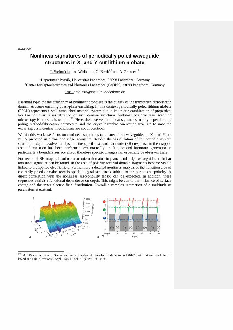
ISAF-P3C-63 ____________________________________________________________________________________________________________________
Nonlinear signatures of periodically poled waveguide
structures in X- and Y-cut lithium niobate
T. Steinrücke1, A. Widhalm
1, G. Berth
1,2 and A. Zrenner
1,2
1Department Physik, Universität Paderborn, 33098 Paderborn, Germany
2Center for Optoelectronics and Photonics Paderborn (CeOPP), 33098 Paderborn, Germany
Email: [email protected]
Essential topic for the efficiency of nonlinear processes is the quality of the transferred ferroelectric
domain structure enabling quasi-phase-matching. In this context periodically poled lithium niobate
(PPLN) represents a well-established material system due to its unique combination of properties.
For the noninvasive visualization of such domain structures nonlinear confocal laser scanning
microscopy is an established tool298
. Here, the observed nonlinear signatures mainly depend on the
poling method/fabrication parameters and the crystallographic orientation/area. Up to now the
occurring basic contrast mechanisms are not understood.
Within this work we focus on nonlinear signatures originated from waveguides in X- and Y-cut
PPLN prepared in planar and ridge geometry. Besides the visualization of the periodic domain
structure a depth-resolved analysis of the specific second harmonic (SH) response in the mapped
area of transition has been performed systematically. In fact, second harmonic generation is
particularly a boundary surface effect, therefore specific changes can especially be observed there.
For recorded SH maps of surface-near micro domains in planar and ridge waveguides a similar
nonlinear signature can be found. In the area of polarity reversal domain fragments become visible
linked to the applied electric field. Furthermore a detailed nonlinear analysis of the transition area of
contrarily poled domains reveals specific signal sequences subject to the period and polarity. A
direct correlation with the nonlinear susceptibility tensor can be expected. In addition, these
sequences exhibit a functional dependence on depth. This might be due to the influence of surface
charge and the inner electric field distribution. Overall a complex interaction of a multitude of
parameters is existent.
a) b)
298
M. Flörsheimer et al., “Second-harmonic imaging of ferroelectric domains in LiNbO3 with micron resolution in
lateral and axial directions”, Appl. Phys. B, vol. 67, p. 593-599, 1998.

Fig. 1: (a) SH intensity as a function of the depth in Y-cut PPLN (period: 16µm, scan increment: 100 nm).
(b) Signal sequences perpendicular to the domain structure in XZ area for three different depths
(red: Y = 0 µm, green: Y = -2.2 µm, blue: Y = -4.5 µm).
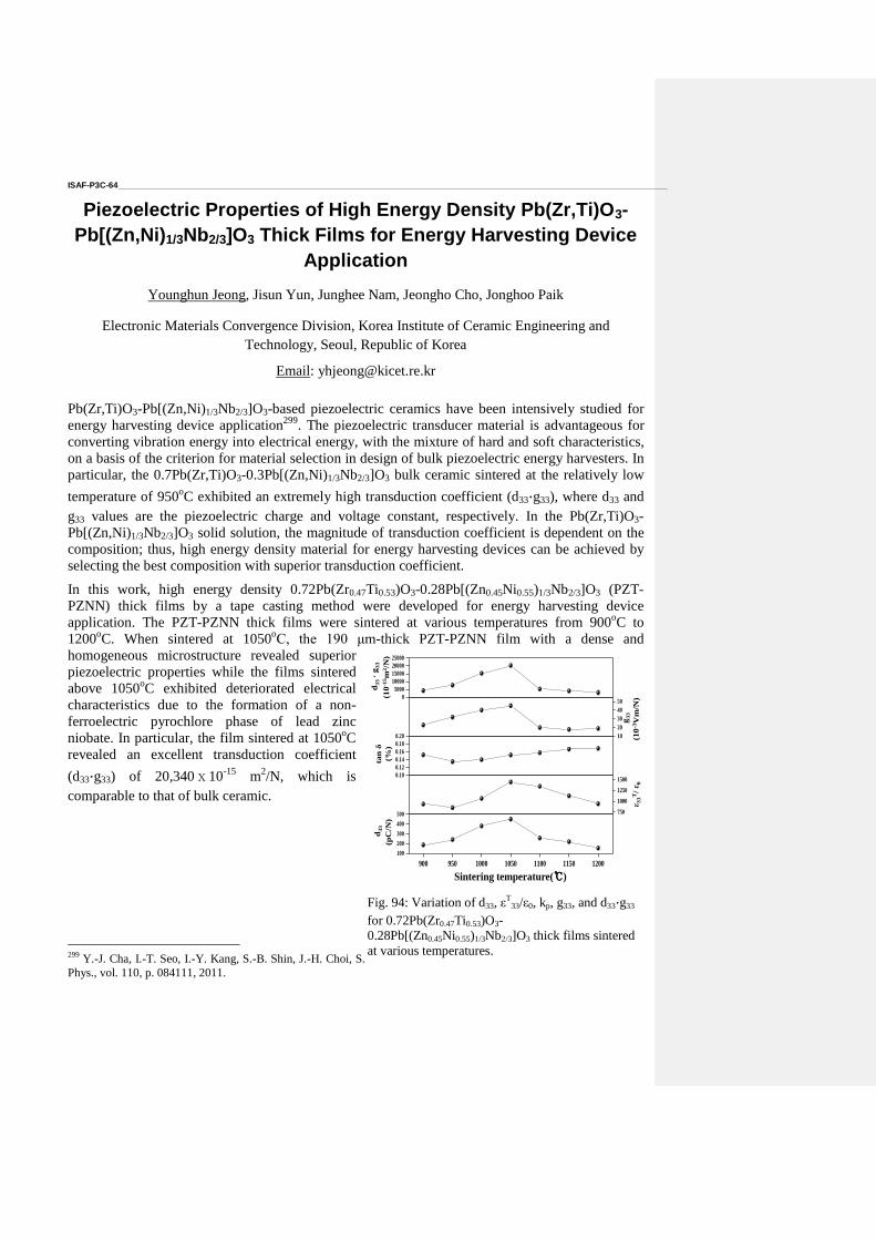
ISAF-P3C-64 ____________________________________________________________________________________________________________________
Piezoelectric Properties of High Energy Density Pb(Zr,Ti)O3-
Pb[(Zn,Ni)1/3Nb2/3]O3 Thick Films for Energy Harvesting Device
Application
Younghun Jeong, Jisun Yun, Junghee Nam, Jeongho Cho, Jonghoo Paik
Electronic Materials Convergence Division, Korea Institute of Ceramic Engineering and
Technology, Seoul, Republic of Korea
Email: [email protected]
Pb(Zr,Ti)O3-Pb[(Zn,Ni)1/3Nb2/3]O3-based piezoelectric ceramics have been intensively studied for
energy harvesting device application299
. The piezoelectric transducer material is advantageous for
converting vibration energy into electrical energy, with the mixture of hard and soft characteristics,
on a basis of the criterion for material selection in design of bulk piezoelectric energy harvesters. In
particular, the 0.7Pb(Zr,Ti)O3-0.3Pb[(Zn,Ni)1/3Nb2/3]O3 bulk ceramic sintered at the relatively low
temperature of 950oC exhibited an extremely high transduction coefficient (d33∙g33), where d33 and
g33 values are the piezoelectric charge and voltage constant, respectively. In the Pb(Zr,Ti)O3-
Pb[(Zn,Ni)1/3Nb2/3]O3 solid solution, the magnitude of transduction coefficient is dependent on the
composition; thus, high energy density material for energy harvesting devices can be achieved by
selecting the best composition with superior transduction coefficient.
In this work, high energy density 0.72Pb(Zr0.47Ti0.53)O3-0.28Pb[(Zn0.45Ni0.55)1/3Nb2/3]O3 (PZT-
PZNN) thick films by a tape casting method were developed for energy harvesting device
application. The PZT-PZNN thick films were sintered at various temperatures from 900oC to
1200oC. When sintered at 1050
oC, the 190 μm-thick PZT-PZNN film with a dense and
homogeneous microstructure revealed superior
piezoelectric properties while the films sintered
above 1050oC exhibited deteriorated electrical
characteristics due to the formation of a non-
ferroelectric pyrochlore phase of lead zinc
niobate. In particular, the film sintered at 1050oC
revealed an excellent transduction coefficient
(d33∙g33) of 20,340ⅹ10-15
m2/N, which is
comparable to that of bulk ceramic.
299
Y.-J. Cha, I.-T. Seo, I.-Y. Kang, S.-B. Shin, J.-H. Choi, S. Nahm, T.-H. Seung, J.-H. Paik, “Title of work”, J. Appl.
Phys., vol. 110, p. 084111, 2011.
d3
3 · g
33
(10
-15m
2/N
)
ε3
3T/
ε0
tan
δ
(%)
g3
3
(10
-3V
m/N
)
d3
3
(pC
/N)
Sintering temperature(℃)
900 950 1000 1050 1100 1150 1200
100
200
300
400
500 750
1000
1250
15000.10
0.12
0.14
0.16
0.18
0.20 10
20
30
40
500
5000
10000
15000
20000
25000
Fig. 94: Variation of d33, εT
33/ε0, kp, g33, and d33∙g33
for 0.72Pb(Zr0.47Ti0.53)O3-
0.28Pb[(Zn0.45Ni0.55)1/3Nb2/3]O3 thick films sintered
at various temperatures.
ISAF-P3C-65 ____________________________________________________________________________________________________________________
Resolved E-symmetry zone-centre phonons in LiTaO3 and
LiNbO3
S. Margueron1, A.Bartasyte
2, A.M. Glazer
3, E. Simon
4, J. Hlinka
4, I. Gregora
4
1Laboratoire Matériaux Optiques, Photonique et Systèmes, EA 4423, Lorraine University and
Supelec, Metz, France 2Institute Jean Lamour, (UMR 7198) CNRS – Lorraine University, Nancy, France 3Department of Physics, Oxford University, Parks Road, Oxford OX1 3PU, UK
4Institute of Physics AS CR, Prague 8, Czech Republic
Email: [email protected]
Lithium niobate and lithium tantalate have been the subject of intense studies because of their
applications in electro-optic, nonlinear-optic, photo-refractive and acoustical devices. The optical
phonon frequencies, damping parameters and intensities are used for the studies of phase
transitions, symmetry, effect of pressure, stress, composition and heterogeneities in thin films,
integrated structures, nano- and bulk materials. It is essential to know the frequencies of all zone-
centre optical phonons in calculations of dielectric constant, oblique modes and electro-optic
coefficients. There is good agreement in the reported frequencies of A1-symmetry phonons of
LiNbO3 and LiTaO3. Nevertheless, over the last fifty years there has been much discussion in the
literature concerning the E-symmetry phonons in these materials. To date, this discussion on the E-
mode assignment is still open.
In this study, all E-symmetry optical phonons at the Γ point of LiNbO3 and LiTaO3 were
experimentally resolved in the spectra measured by infrared and Raman spectroscopy300
. For this
purpose, congruent and nearly stoichiometric crystals of LiNbO3 and LiTaO3, and mixed LiNb1-
xTaxO3, crystals were studied. The results show that some of the E modes have weak intensities in
Raman or infrared spectra. Thus, the complete assignment of E-symmetry modes has been achieved
by comparing Raman and infrared data. The wavenumbers of the E-modes, estimated
experimentally, were close to those calculated theoretically for LN. The clamped relative ordinary
and extraordinary permittivities of LN and LT were calculated using LST relation with good
agreement with Terahertz Time Domain spectroscopy.
300
S. Margueron, A. Bartasyte, A.M. Glazer, E. Simon, J. Hlinka, I. Gregora, and J. Gleize, J. Appl. Phys. 111, 104105,
2012.
ISAF-P3C-66 ____________________________________________________________________________________________________________________
Infrared Photoluminescence in Er Doped Bismuth Layered Ferroelectrics
Dengfeng Peng, Hua Zou, Xusheng Wang301
, and Xi Yao
(Functional Materials Research Laboratory, Tongji University, 1239 Siping Road, Shanghai 200092,
China)
Abstract: For ferroelectric materials, doping is usually applied to modify electronic properties,
such as dielectric, ferroelectric, and piezoelectric properties. Recently, multifunctionality has
renewed the interest in ferroelectrics, such as ferroelectric-photo, ferroelectric–elastic, ferroelectric–
elastic–magnetic, ferroelectric– mechanical, integration and/or coupling, which can lead to a
remarkable progress with numerous new materials and devices for photovoltaic, spintronic and
optical-electrical-mechanical actuator and sensor applications. Here we examine the Er3+
doped
CaBi4Ti4O15 bismuth layered structured ferroelectrics (BLSF) and demonstrate that a certain
amount of Er3+
doped ceramic sample shows an infrared photoluminescence while simultaneously
keeping ferroelectric characteristics. Photoluminescence excitation spectra show that the samples
have broad excitations from ultraviolet to green regions. The ultraviolet excitation is associated with
the electronic transition within the host solid and the green excitation corresponds to the f-f
transitions of Er3+
, respectively. Upon these excitations, the doped samples show a strong infrared
emission at room temperature, corresponding to 4I13/2→
4I15/2 transition of Er
3+. The infrared
photoluminescence of Er3+
reported here has also been discovered in a variety of BLSF oxides such
as BaBi4Ti4O15 SrBi4Ti4O15 and CaBi2Ta2O9 et al., and as series of multifunctional ferroelectrics,
Er3+
doped BLSF materials would be of great importance for the fundamental study of optical-
electrical-mechanical couplings and multifunctional design of future optical-electrical integrated
devices.
301 Corresponding author. Tel.: +86 21 65980544; fax: +86 2165985179;
E-mail: [email protected]; [email protected].
ISAF-P3C-67 ____________________________________________________________________________________________________________________
Dielectric Characterization of PLZST
Theresa Kainz1, Michael Naderer
1, Denis Schütz
1, Klaus Reichmann
1
1 CD-Laboratory for Advanced Ferroic Oxides, University of Technology, Graz, Austria
Email: [email protected]
Lead zirconate – lead titanate, in short PZT, is a well-known and widespread ferroelectric material
for many applications such as actuators, sensors, transducers and further more.
In the zirconium rich region of the solid solution its structural properties are changing causing a
distortion of the unit cell and opposed neighboring electric dipoles inside the cell resulting in a zero
net spontaneous polarization transforming a ferroelectric material to an antiferroelectric one. The
substitution of lead by aliovalent lanthanum stabilizes the antiferroelectric phase. Applying an
electric field higher than a critical switching field converts the anti-parallel to a parallel dipole
alignment inducing a ferroelectric state. Removing the field reverses the alignment to the
antiferroelctric phase releasing the stored polarization and producing a current. The change in the
structure enables to store charge and energy respectively at higher electric fields where
conventional ferroelectric materials deteriorate in permittivity.
In this work the electric field induced antiferroelectric-to-ferroelectric phase transition of lanthanum
modified lead zirconate titanate stannate ceramics was investigated in order to clarify the role of tin.
The compositions varied in the tin content replacing the zirconium (Pb0,91La0,06VPb´´0,03)(Zr0,90-
xTi0,1Snx)O3 (x = 0,01-0,24) were located in the antiferroelectric phase region.
The ceramic was prepared by the conventionally mixed oxide route with an excess of lead added
before calcination. The mixture was calcined at 850°C and sintering was performed at 1250°C for 3
hours.
Dielectric behavior was investigated by measuring the low signal permittivity, capacitance and the
piezoelectric coefficient d33 as well as recording the polarization curves. To display the
microstructure scanning electron microscopy was used in the channeling contrast mode instead of
etching. Furthermore the chemical composition of the as-prepared ceramic could be identified with
energy dispersive x-ray spectroscopy.
ISAF-P3C-68 ____________________________________________________________________________________________________________________
Dielectric relaxations and polarons in Sn2P2S6 ferroelectrics
A. Dziaugys1, J. Banys
1, M. Medulych
2, A. Molnar
2, Yu. Vysochanskii
2
1 Faculty of Physics, Vilnius University, Lithuania
2 Institute of Physics and Chemistry of Solid State, Uzhgorod University, Ukraine
Email: [email protected]
For Sn2P2S6 ferroelectrics the second order phase transition at T0 ≈ 337 K is related with
nonlinear interaction of the fully symmetrical and soft polar optic modes. The stereoactivity of tin
cations lone pair electrons determines the chemical bonds changes and charge transfer at transition
into the ferroelectric phase [1,2]. Semiconductive properties of these crystals are determined by
sulfur vacancies deep donor states and tin vacancies shallow acceptor states in the energy gap. The
deep energy level of small electron polarons, which are selftrapped at Sn+ cations, and shallow
energy levels of small hole polarons that are trapped at S- anions also induce the local states in the
gap [3]. The dielectric spectroscopy for the temperature interval 20 – 380 K have been applied for
studying of slow dynamics of the polaronic particles in by vapor transpot and Bridgemann methods
grown Sn2P2S6 crystals. The dielectric relaxation anomaly was found with dielectric losses
maximum near 60 K at low frequencies. Also two losses peaks were observed in 160 – 260 K
temperature range. Observed dielectric relaxation anomalies are explained by small hole polarons
dynamics with donor-acceptor compensation processes in lattice with tin and sulfur vacancies.
1. Yu. M. Vysochanskii, T. Janssen, R. Currat, R. Folk, J. Banys, J. Grigas, V. Samulionis
(Vilnius University Publishung House, Vilnius, 2006).
2. K. Rushchanskii, Yu. Vysochanskii, D. Strauch, Phys. Rev. Letters, 99, 207601 (2007).
3. Yu. Vysochanskii, A. Molnar, R. Yevych, K. Glukhov, M. Medulych, Ferroelectrics, 438, 55
(2012).
Acknowledgment
We wish to acknowledge the support of the Research Council of Lithuania funding this work
according to the project “Postdoctoral Fellowship Implementation in Lithuania”.
ISAF-P3C-69 ____________________________________________________________________________________________________________________
Magnetostriction and magnetoelectric effect in
intermetallic/relaxor/PVDF composites
Guzdek Piotr1
1Department of Microelectronics, Institute of Electron Technology, Cracow Division, Zablocie St.
39, 30-701 Cracow, Poland
Email: [email protected]
Magnetostrictive and magnetoelectric materials, a class of smart materials, are drawing much
attention due to their practical applications. Magnetostriction has been defined as an elastic strain
causing a change in shape of material during magnetization. In the magnetic field magnetostrictive
material reorientates its magnetic domains, so it causes physical length change in the material.
Magnetoelectric effect is defined as an induced dielectric polarization under an applied magnetic
field. In the past decade, smart materials have attracted increasing interesting because of their
practical applications in sensors, actuators, memory devices, transducers, filters, waveguides,
switches, phase invertors
Magnetoelectric effect in bulk and multilayer structures consisting of intermetallic compounds as
magnetostrictive phase and ferroelectric relaxors and PVDF as piezoelectric phase was investigated.
This paper describes the synthesis and tape casting process for ferrimagnetic Tb0.27−xDy0.73−yAx+yFe2
compounds (A = Y, Tb, Yb) and ferroelectric Pb(Fe0.5Ta0.5)O3, Pb(Fe0.5Nb0.5)O3 relaxors. All the
composites were characterized by scanning electron microscope observations and complex
impedance analysis. Magnetostrictive and ferroelectric grains were distributed homogeneous in a
PVDF matrix. Complex impedance and dielectric permittivity of bulk and layered composites were
studied in a temperature range from –40 to 150°C and frequency range 10 Hz - 2 MHz. Magnetic
hysteresis and magnetization were measured by a vibrating sample magnetometer (VSM) in an
applied magnetic field up to 85 kOe at temperature range from 4K to 400K. The magnetic
hysteresis determined for composites are typical of a mixture of the soft magnetic material with a
significant amount of the paramagnet. The bifurcation of ZFC-FC magnetizations observed for both
composites implies spin-glass behavior. Magnetostriction measurements at room temperature were
carried out using Strain Gauge Technique in range of static magnetic field (300-7200 Oe).
Magnetoelectric effect at room temperature was investigated as a function of static magnetic field
(300-7200 Oe) and frequency (10 Hz-10 kHz) of sinusoidal modulation magnetic field (5-20 Oe).
Both types of composites exhibit a distinct magnetoelectric effect.
ISAF-P3C-70 ____________________________________________________________________________________________________________________
High-Temperature Structural Transitions in YMn1-xTixO3
M. Tomczyk1, P.M. Vilarinho
1, V.V. Laguta
2, I. Levin
3
1 Department of Ceramics and Glass Engineering, University of Aveiro, 3810-193 Aveiro, Portugal
2 Institute of Physics AS CR, Cukrovarnicka 10, 162 53 Prague, Czech Republic
3 Materials Measurement Science Division, NIST, Gaithersburg, MD 20899,USA
Email: [email protected].
YMnO3, which at ambient pressure crystallizes with a layered hexagonal structure, has attracted
much interest because of its multiferroic properties302
. YMnO3 undergoes two phase transitions: a
non-polar to polar (P63/mmc to P63cm) transition at 1273 K303
, which is accompanied by tripling of
the unit-cell volume, and a subtle, isosymmetric, (P63cm to P63cm) transition at 920 K304
. This
lower temperature phase transition, the nature of which still remains uncertain, has been associated
with the Curie temperature (TC) of YMnO3. However, recent neutron diffraction studies of
YMnO3305
suggested that the macroscopic polarization is non-zero even above TC and drops
abruptly below Tc. These results, which remained uncommented in the literature, question our
understanding of the ferroelectric transition in YMnO3.
In the present study, we used variable-temperature X-ray and neutron diffraction to examine the
effects of Ti substitutions in YMn1-xTixO3 (0<x<0.15) solid solutions on the phase transitions in this
system. The temperature of the high-temperature transition P63/mmc-P63/cm decreases
continuously as x increases. At lower temperatures (from 650 K to 800 K, depending on x), we
observed an anomalous behavior of the c-lattice parameter, which appears to be connected to an
isosymmetric transition of the type seen in YMnO3. In YMnO3, structural parameters are
independent of the sample atmosphere. By contrast, in YMn1-xTixO3, the structural anomalies vary
markedly with the atmosphere, suggesting strong effects of point defects induced by the substitution
of Ti on the supposed structural transition. Apparently, the presence of point defects enhances the
structural changes associated with this transition. In the talk, we will discuss our findings that
provide new insights into the nature of structural transitions in YMnO3 and Y(Mn,Ti)O3 solid
solutions.
302
W. Prellier, M.P. Singh, P. Murugvel, J. Phys.: Condens. Matter, vol.17, R803, 2005. 303
K. Lukaszewicz, J. Karut-Kalicinska, Ferroelectrics, vol. 7, 81,1974. 304
I.G. Ismailzade, S.A. Kizhaev, Sov. Phys. Solid. State, vol.7, 236, 1965. 305
A.S. Gibbs, K.S. Knight, P. Lightfoot, Phys. Rev. B, vol. 83,184418, 2005.

Piezoelectric MEMS
CLUB A
Thursday, July 25 2013, 08:30 am - 10:00 am
Chair: Paul Muralt
EPFL
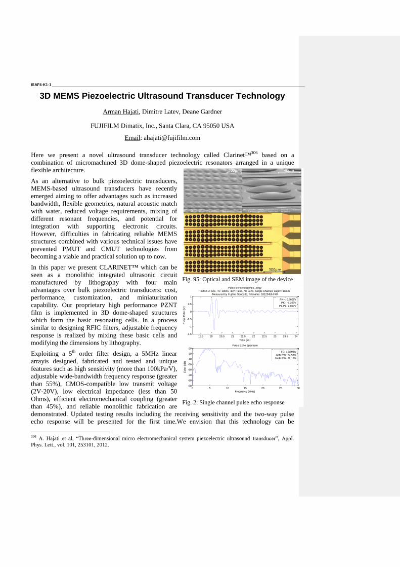
ISAF4-K1-1 _____________________________________________________________________________________________________________________
3D MEMS Piezoelectric Ultrasound Transducer Technology
Arman Hajati, Dimitre Latev, Deane Gardner
FUJIFILM Dimatix, Inc., Santa Clara, CA 95050 USA
Email: [email protected]
Here we present a novel ultrasound transducer technology called Clarinet™306
based on a
combination of micromachined 3D dome-shaped piezoelectric resonators arranged in a unique
flexible architecture.
As an alternative to bulk piezoelectric transducers,
MEMS-based ultrasound transducers have recently
emerged aiming to offer advantages such as increased
bandwidth, flexible geometries, natural acoustic match
with water, reduced voltage requirements, mixing of
different resonant frequencies, and potential for
integration with supporting electronic circuits.
However, difficulties in fabricating reliable MEMS
structures combined with various technical issues have
prevented PMUT and CMUT technologies from
becoming a viable and practical solution up to now.
In this paper we present CLARINET™ which can be
seen as a monolithic integrated ultrasonic circuit
manufactured by lithography with four main
advantages over bulk piezoelectric transducers: cost,
performance, customization, and miniaturization
capability. Our proprietary high performance PZNT
film is implemented in 3D dome-shaped structures
which form the basic resonating cells. In a process
similar to designing RFIC filters, adjustable frequency
response is realized by mixing these basic cells and
modifying the dimensions by lithography.
Exploiting a 5th
order filter design, a 5MHz linear
arrayis designed, fabricated and tested and unique
features such as high sensitivity (more than 100kPa/V),
adjustable wide-bandwidth frequency response (greater
than 55%), CMOS-compatible low transmit voltage
(2V-20V), low electrical impedance (less than 50
Ohms), efficient electromechanical coupling (greater
than 45%), and reliable monolithic fabrication are
demonstrated. Updated testing results including the receiving sensitivity and the two-way pulse
echo response will be presented for the first time.We envision that this technology can be
306
A. Hajati et al, “Three-dimensional micro electromechanical system piezoelectric ultrasound transducer”, Appl.
Phys. Lett., vol. 101, 253101, 2012.
Fig. 95: Optical and SEM image of the device
19.5 20 20.5 21 21.5 22 22.5 23 23.5 24-1.5
-1
-0.5
0
0.5
1
Pulse Echo Response, 2way
FDMX LF-Mix, Tx: 100ns, 40V Pulse, No Lens, Single Channel, Depth: 15mm
Measured by Fujifilm Sonosite, Filename: 18123456.F40
Time (s)
Puls
e E
cho (
V)
0 5 10 15 20 25 30-90
-80
-70
-60
-50
-40
-30
-20Pulse Echo Spectrum
Frequency (MHz)
Echo (
dB
)
FC: 4.38MHz
6dB BW: 64.53%
10dB BW: 78.12%
PK+: 0.8606V
PK-: -1.263V
Pk-Pk: 2.017V
Fig. 2: Single channel pulse echo response

implemented as a desirable solution in high performance 3D/4D, low-power portable and in-vivo
imaging systems.
ISAF4-K1-2 _____________________________________________________________________________________________________________________
Ferroelectric Film Bulk Acoustic Wave Resonators for Liquid
Viscosity Sensing
Andrei Vorobiev and Spartak Gevorgian
Department of Microtechnology and Nanoscience, Chalmers University of Technology,
Gothenburg, Sweden
Email: [email protected]
The piezoelectric film bulk acoustic wave (BAW) resonators have proven to be suitable for application
as high accuracy and CMOS-compatible liquid viscosity sensors. However, the non-ferroelectric BAW
sensors, usually operating in thickness shear mode, always have a longitudinal wave component
generated as by-product due to inclination of polarization. The longitudinal contribution leads to a fluid
turbulence at the device surface, which disturbs the conditions of the shear viscosity measurements. In
the proposed paper we present, for the first time, the concept of the liquid viscosity sensing with the
ferroelectric BAW resonators allowing for realization of truly shear displacement. The advantage of the
ferroelectric based sensors is associated with the nature of the dc field induced piezoelectric effect. The
induced polarization strictly coincides with the electric field. This allows for exclusively shear
displacement and, hence, laminar shear of fluid at the resonator vertical side walls.
The sensors have been fabricated as the BAW solidly
mounted resonators, based on the 0.67BiFeO3-
0.33BaTiO3 multiferroic films307, operating at
4.2 GHz resonant frequency and 10 V dc bias. In the
experiments the resonators have been covered by
layers of liquids with different viscosity and thickness
controlled to be about 250 µm.
The measured resonator response has been analyzed
using the proposed model of a harmonic oscillator
damped by a viscous force in the form of the Stokes’
low. It can be seen from Fig. 1 that the hyperbolic
dependence of the resonator Q-factor, predicted by
the model, agrees well with the measurements. The
sensitivity of the resonator with the Q=200 is ca
10 (mPa s)-1, which is high enough for the accurate
characterization of water and other low viscosity liquids. Analysis indicates that the resonator effective
mass is much larger than the added mass of the liquids, which explains the observed insensitivity of the
Q-factor and resonance frequency to the liquid layer thickness. This makes the measurements simpler
and more accurate since does not involve the liquid layer thickness and mass density.
Another advantage of the proposed sensors is possibility of simultaneous monitoring of the liquid
temperature using inherent temperature dependence of the ferroelectric permittivity. This is a very
useful feature, since the viscosity of many liquids is strongly temperature dependent. Estimates show
that the temperature can be monitored with accuracy of ca 0.01 K.
307
A. Vorobiev, S. Gevorgian, N. Martirisyan, M. Löffler, and E. Olsson “Intrinsically tunable
0.67BiFeO3-0.33BaTiO3 thin film bulk acoustic wave resonators”, Appl. Phys. Lett., vol. 101, p. 232903 -5, 2012.
Fig. 96: Q-factors and sensitivity of the
ferroelectric BAW vs. viscosity. The Q-factor
dependence lines are hyperbolic fitting curves.

ISAF4-K1-3 _____________________________________________________________________________________________________________________
New Human Machine Interface Devices Using
a Piezoelectric Poly(L-lactic acid) Film
Masamichi Ando1,2
, Hideki Kawamura1, Hiroaki .Kitada
1, Takafumi .Inoue
1, Yoshiro Tajitsu
2
1Organic Film Devices Project/Murata Manufacturing Co. ,Ltd., Nagaokakyo-shi, Kyoto/Japan
2Graduate School of Engineering/Kansai University, Suita-shi, Osaka/Japan
Email: [email protected]
Poly(lactic acid) (PLA) has become widely known as an
ecofriendly biomass polymer. The lactic acid monomer has an
asymmetric carbon; thus, it has chirality. If the L-lactide is
polymerized, then the PLA polymer is called an L-type PLA or a
poly(L-lactic acid) (PLLA). If the polymer undergoes drawing or
elongation, then they exhibit shear piezoelectricity308. In
collaboration with Mitsui Chemicals, we have produced a stable
PLLA film with a sufficient piezoelectric constant to be used for
sensing applications309. The piezoelectric PLLA film does not
have pyroelectricity, because it does not have intrinsic
polarization. Therefore, even if the PLLA film is used for a
human-machine interface (HMI), which operates by direct
operation by hand, there is no incorrect detection due to heat.
It has been recognized that a capacitive-type touch panel (CTP)
is a very useful HMI for a smart phone and a tablet type personal
computer. The touch panel with a pressure recognition function has been
desired for more often these days. The PLLA film is very suitable for a
CTP as a pressure sensing film. Pressure due to the slight bending of the
glass during touch screen applications can be detected accurately.
Furthermore, because the PLLA has very high transparency, it is suitable
for touch panel pressure sensing, in which transparency is required. Figure
1 shows the relationship between the load on the glass and the generated
electric charge. The PLLA film is attached on the glass. The glass size is
110(L)×60(W)×0.5(T) mm. The PLLA film forming the electrode on both
principal surfaces is 0.07 mm in thickness and has a piezoelectricity, d14 =
6.0 pC N−1. The four sides of the glass are attached to a case,
approximately the size of a smart phone. Although there is some difference
in the sensitivity due to the position of the applied pressure, the sensitivity
can be equalized and linearized by combining it with position detection
information. Figure 2 shows an example of multiple electrodes formed on
the PLLA film, which consists of a pressure detection electrode and an
electrode for the CTP. Additional electrode layers are not required with such a composition; thus, the
resulting pressure detection touch panel is highly transparent.
1 E. Fukada: IEEE Trans. Dielectr. Electr. Insul. 13 (2006) 1110.
2 M. Ando, H. Kawamura, K. Kageyama, and Y. Tajitsu: Jpn. J. Appl. Phys. 51 (2012) 09LD14
0
200
400
600
800
1000
1200
1400
1600
0 200 400 600
Ele
ctri
c ch
arg
e (p
C)
Load (g)
A B C D
Fig.1: Relationship between the applied
load and generated electric charge.
A
A
TX
RX
TX
Z
Z
RX
(a) Top view
TX TX
RX RX
Z Z
ZZ Z
PLLA
(b) AA-Cross-sectional view
Fig.2: Multiple electrodes.
20
20
20
11
0
60
A
B
C D
(mm)

ISAF4-K1-4 _____________________________________________________________________________________________________________________
Piezoelectric Microelectromechanical Systems (MEMS) Across Length Scales
R. Johnson, D. Wilke, C. Yeager, T. N. Jackson, and S. Trolier-McKinstry: Penn State
P. Reid, V. Cotroneo, and D. Schwartz: SAO
D. Newns, G. Martyna, T. Shaw, M. Copel, T. Theis: IBM
Abstract
Piezoelectric thin films are of increasing interest in low voltage microelectromechanical
systems (MEMS) for sensing, actuation, and energy harvesting. They also serve as model systems
to study fundamental behavior in piezoelectrics. Piezoelectric MEMS devices range over a wide
range of length scales. On the extreme upper end are large area devices for applications such as
adaptive optics. In this case, the piezoelectric film can be used to produce local deformation of a
mirror surface, in order to correct figure errors associated with fabrication of the component or to
correct for atmospheric distortion. For example, should a mission such as Gen-X be flown, it would
require up to 10,000 m2 of actuatable optics in order to correct the figures of the nested hyperboloid
reflecting segments. In this case, the “micro” in “microelectromechanical systems” is clearly a
misnomer, although the fabrication techniques would involve conventional micromachining for
patterning of the electrodes. Many piezoelectric MEMS devices are fabricated at intermediate
length scales (tens of microns to 1 cm). Here, examples will be given of piezoelectric energy
harvesting devices. We have recently demonstrated improvements in the energy harvesting figure
of merit for the piezoelectric layer by factors of 4 – 10. Finally, piezoelectric MEMS are also
attracting attention at a substantially smaller size scale (tens of nm) as a potential replacement for
CMOS electronics. Examples of the materials choice as well as specific devices at all three of these
length scales will also be discussed.
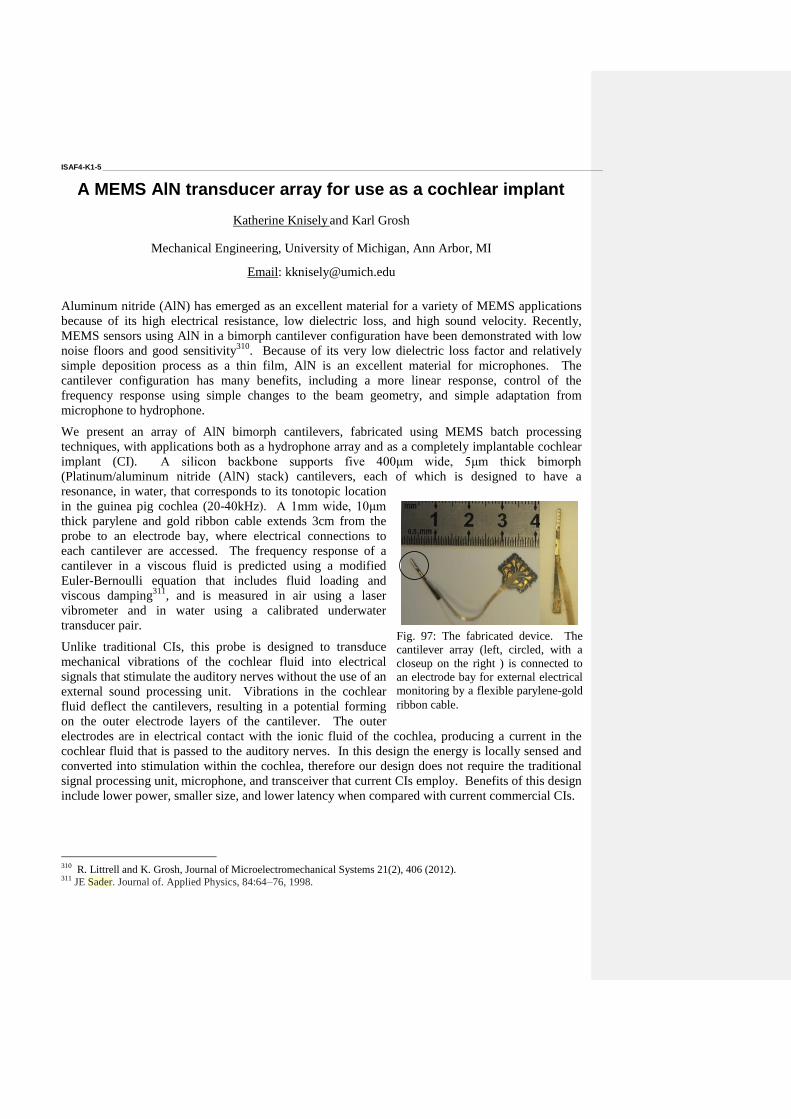
ISAF4-K1-5 _____________________________________________________________________________________________________________________
A MEMS AlN transducer array for use as a cochlear implant
Katherine Knisely and Karl Grosh
Mechanical Engineering, University of Michigan, Ann Arbor, MI
Email: [email protected]
Aluminum nitride (AlN) has emerged as an excellent material for a variety of MEMS applications
because of its high electrical resistance, low dielectric loss, and high sound velocity. Recently,
MEMS sensors using AlN in a bimorph cantilever configuration have been demonstrated with low
noise floors and good sensitivity310
. Because of its very low dielectric loss factor and relatively
simple deposition process as a thin film, AlN is an excellent material for microphones. The
cantilever configuration has many benefits, including a more linear response, control of the
frequency response using simple changes to the beam geometry, and simple adaptation from
microphone to hydrophone.
We present an array of AlN bimorph cantilevers, fabricated using MEMS batch processing
techniques, with applications both as a hydrophone array and as a completely implantable cochlear
implant (CI). A silicon backbone supports five 400μm wide, 5μm thick bimorph
(Platinum/aluminum nitride (AlN) stack) cantilevers, each of which is designed to have a
resonance, in water, that corresponds to its tonotopic location
in the guinea pig cochlea (20-40kHz). A 1mm wide, 10μm
thick parylene and gold ribbon cable extends 3cm from the
probe to an electrode bay, where electrical connections to
each cantilever are accessed. The frequency response of a
cantilever in a viscous fluid is predicted using a modified
Euler-Bernoulli equation that includes fluid loading and
viscous damping311
, and is measured in air using a laser
vibrometer and in water using a calibrated underwater
transducer pair.
Unlike traditional CIs, this probe is designed to transduce
mechanical vibrations of the cochlear fluid into electrical
signals that stimulate the auditory nerves without the use of an
external sound processing unit. Vibrations in the cochlear
fluid deflect the cantilevers, resulting in a potential forming
on the outer electrode layers of the cantilever. The outer
electrodes are in electrical contact with the ionic fluid of the cochlea, producing a current in the
cochlear fluid that is passed to the auditory nerves. In this design the energy is locally sensed and
converted into stimulation within the cochlea, therefore our design does not require the traditional
signal processing unit, microphone, and transceiver that current CIs employ. Benefits of this design
include lower power, smaller size, and lower latency when compared with current commercial CIs.
310
R. Littrell and K. Grosh, Journal of Microelectromechanical Systems 21(2), 406 (2012). 311
JE Sader. Journal of. Applied Physics, 84:64–76, 1998.
Fig. 97: The fabricated device. The
cantilever array (left, circled, with a
closeup on the right ) is connected to
an electrode bay for external electrical
monitoring by a flexible parylene-gold
ribbon cable.


Modeling: multiscale, first-principles,...
CLUB B
Thursday, July 25 2013, 08:30 am - 10:00 am
Chair: George Rossetti
University of Connecticut
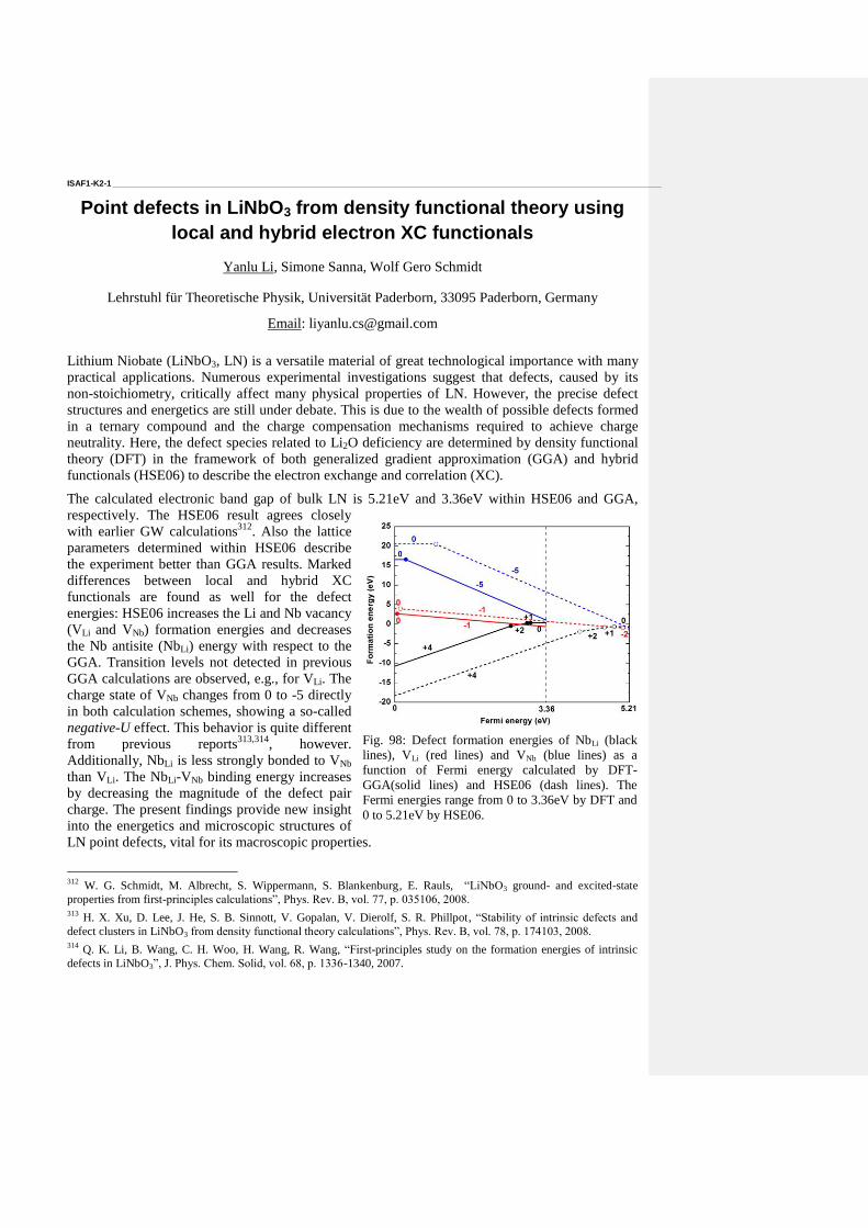
ISAF1-K2-1 _____________________________________________________________________________________________________________________
Point defects in LiNbO3 from density functional theory using
local and hybrid electron XC functionals
Yanlu Li, Simone Sanna, Wolf Gero Schmidt
Lehrstuhl für Theoretische Physik, Universität Paderborn, 33095 Paderborn, Germany
Email: [email protected]
Lithium Niobate (LiNbO3, LN) is a versatile material of great technological importance with many
practical applications. Numerous experimental investigations suggest that defects, caused by its
non-stoichiometry, critically affect many physical properties of LN. However, the precise defect
structures and energetics are still under debate. This is due to the wealth of possible defects formed
in a ternary compound and the charge compensation mechanisms required to achieve charge
neutrality. Here, the defect species related to Li2O deficiency are determined by density functional
theory (DFT) in the framework of both generalized gradient approximation (GGA) and hybrid
functionals (HSE06) to describe the electron exchange and correlation (XC).
The calculated electronic band gap of bulk LN is 5.21eV and 3.36eV within HSE06 and GGA,
respectively. The HSE06 result agrees closely
with earlier GW calculations312
. Also the lattice
parameters determined within HSE06 describe
the experiment better than GGA results. Marked
differences between local and hybrid XC
functionals are found as well for the defect
energies: HSE06 increases the Li and Nb vacancy
(VLi and VNb) formation energies and decreases
the Nb antisite (NbLi) energy with respect to the
GGA. Transition levels not detected in previous
GGA calculations are observed, e.g., for VLi. The
charge state of VNb changes from 0 to -5 directly
in both calculation schemes, showing a so-called
negative-U effect. This behavior is quite different
from previous reports313,314
, however.
Additionally, NbLi is less strongly bonded to VNb
than VLi. The NbLi-VNb binding energy increases
by decreasing the magnitude of the defect pair
charge. The present findings provide new insight
into the energetics and microscopic structures of
LN point defects, vital for its macroscopic properties.
312
W. G. Schmidt, M. Albrecht, S. Wippermann, S. Blankenburg, E. Rauls, “LiNbO3 ground- and excited-state
properties from first-principles calculations”, Phys. Rev. B, vol. 77, p. 035106, 2008. 313
H. X. Xu, D. Lee, J. He, S. B. Sinnott, V. Gopalan, V. Dierolf, S. R. Phillpot, “Stability of intrinsic defects and
defect clusters in LiNbO3 from density functional theory calculations”, Phys. Rev. B, vol. 78, p. 174103, 2008. 314
Q. K. Li, B. Wang, C. H. Woo, H. Wang, R. Wang, “First-principles study on the formation energies of intrinsic
defects in LiNbO3”, J. Phys. Chem. Solid, vol. 68, p. 1336-1340, 2007.
Fig. 98: Defect formation energies of NbLi (black
lines), VLi (red lines) and VNb (blue lines) as a
function of Fermi energy calculated by DFT-
GGA(solid lines) and HSE06 (dash lines). The
Fermi energies range from 0 to 3.36eV by DFT and
0 to 5.21eV by HSE06.
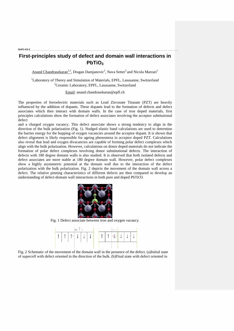
ISAF1-K2-2 _____________________________________________________________________________________________________________________
First-principles study of defect and domain wall interactions in
PbTiO3
Anand Chandrasekaran1,2
, Dragan Damjanovic2, Nava Setter
2 and Nicola Marzari
1
1Laboratory of Theory and Simulation of Materials, EPFL, Lasusanne, Switzerland
2Ceramic Laboratory, EPFL, Lasusanne, Switzerland
Email: [email protected]
The properties of ferroelectric materials such as Lead Zirconate Titanate (PZT) are heavily
influenced by the addition of dopants. These dopants lead to the formation of defects and defect
associates which then interact with domain walls. In the case of iron doped materials, first
principles calculations show the formation of defect associates involving the acceptor subtitutional
defect
and a charged oxygen vacancy. This defect associate shows a strong tendency to align in the
direction of the bulk polarization (Fig. 1). Nudged elastic band calculations are used to determine
the barrier energy for the hopping of oxygen vacancies around the acceptor dopant. It is shown that
defect alignment is likely responsible for ageing phenomena in acceptor doped PZT. Calculations
also reveal that lead and oxygen divacancies are capable of forming polar defect complexes which
align with the bulk polarization. However, calculations on donor doped materials do not indicate the
formation of polar defect complexes involving donor substitutional defects. The interaction of
defects with 180 degree domain walls is also studied. It is observed that both isolated defects and
defect associates are more stable at 180 degree domain wall. However, polar defect complexes
show a highly asymmetric potential at the domain wall due to the interaction of the defect
polarization with the bulk polarization. Fig. 2 depicts the movement of the domain wall across a
defect. The relative pinning characteristics of different defects are then compared to develop an
understanding of defect-domain wall interactions in both pure and doped PbTiO3.
Fig. 1 Defect associate between iron and oxygen vacancy.
Fig. 2 Schematic of the movement of the domain wall in the presence of the defect. (a)Initial state
of supercell with defect oriented in the direction of the bulk. (b)Final state with defect oriented in

the opposite direction of the bulk. This temporary disalignment is the driving force for ageing and
loop pinching
ISAF1-K2-3 _____________________________________________________________________________________________________________________
Self-Consistent Modeling of the Depolarization Field
Evolution during Polarization Switching in Polycrystalline
Ferroelectrics
Yuri A. Genenko, Jens Wehner, Heinz von Seggern
Institute of Materials Science/Technische Universität Darmstadt, Darmstadt, Germany
Email: [email protected]
The development of polarization during switching in thin ferroelectric films315,316
as well as in bulk
polycrystalline ferroelectrics317
exhibits a slowing down at long poling times in contrast to the
predictions of the classical Kolmogorov-Avrami-Ishibashi model with a single switching time.
This phenomenon is often interpreted as a dispersive polarization reversal characterized by a wide
spectrum of switching times1-3
. On the other hand, such interpretations typically ignore the feed-
back effect of the depolarization field changing during polarization switching. Recently an attempt
to account for this effect in a thin ferroelectric film was made by Lou in a self-consistent one-
dimensional model318
, which resulted in switching curves similar to those of the experiment2.
In the current communication it will be shown that identical results can be obtained by solving a
single first-order differential equation which self-consistently describes the polarization
switching319
instead of using a system of 100 coupled differential equations4. Furthermore, by
combining this equation with two-dimensional finite-element calculations of the depolarization field
a model for the self-consistent analysis of the polarization response in bulk disordered ferroelectrics
accounting for both the statistical distribution of switching times and the feed-back effect of the
depolarization fields was developed for the first time. The results are compared with previous
statistical descriptions of disordered ferroelectric systems.
315
A.K. Tagantsev, I. Stolichnov, N. Setter, J. S. Cross, M. Tsukada, “Non-Kolmogorov-Avrami switching kinetics in
ferroelectric thin films”, Phys. Rev. B, vol. 66, 214109, 2002. 316
J.Y. Jo, H.S. Han, J.-G. Yoon, T.K. Song, S.-H. Kim, and T.W. Noh, “Domain switching kinetics in disordered
ferroelectric thin films”, Phys. Rev. Lett., vol. 99, 267602, 2007. 317
Y.A. Genenko, S. Zhukov, S.V. Yampolskii, J. Schütrumpf, R. Dittmer, W. Jo, H. Kungl , M.J. Hoffmann, and H.
von Seggern, “Universal polarization switching behavior of disordered ferroelectrics”, Adv. Funct. Mater. vol. 22, p.
2058-2066, 2012. 318
X.J. Lou, “Statistical switching kinetics of ferroelectrics”, J. Phys.: Condens. Matter, vol. 21, 012207, 2009. 319
H. von Seggern and G.F. Leal Ferreira, "Switching dynamics in poly(vinylidene fluoride) and copolymers", Appl.
Phys. Lett., vol. 83, p. 3353-3355, 2003.
ISAF1-K2-4 _____________________________________________________________________________________________________________________
FBAR tuning from first principles and high-order electrostriction
Alexander Kvasov1, Alexander Tagantsev
1
1Ceramics Laboratory, École Polytechnique Fédérale de Lausanne, Lausanne, Switzerland
Email: [email protected]
Tunable thin film bulk acoustic wave resonators (TFBARs) based on BaxSr1-xTiO3 (BST) thin films
are considered for frequency agile applications due to the DC bias dependent parameters of the
resonator. TFBARs seem to be a very attractive component for microwave applications since they
offer possibilities to increase the functionality of telecommunication systems. At the same time, for
practical application as tunable microwave filters simultaneous tuning of resonance and
antiresonance frequencies is highly desired.
In [1] it was demonstrated that, for TFBAR antiresonance frequency fAR tuning, it is important to
take into account nonlinear electrostriction m111 ( ...2
... 2
1
2
1111 uP
mF ) which being traditionally
neglected [2] is unknown experimentally.
In this work m111 was calculated for the first time using ab initio methods for BST (Table I). To
improve the reliability of the obtained results we used two different packages: Vienna Ab-initio
Simulation Package (VASP) and Quantum ESPRESSO (QE).
Table 1. Data obtained with the first principles
calculations. m111 - nonlinear electrostriction
coefficient.
It was established that for BST based TFBARs the antiresonance tuning is smaller than previously
made estimations. Our calculations demonstrate the importance of taking into account both
nonlinear electrostriction m111 and background permittivity εb which are equally responsible for the
tuning (Fig. 1).
Figure 1. Modelled dependences of antiresonance
frequency fAR tuning on relative tunability nr for
the TFBAR using the [001]-oriented thin film of
BST with x=0.25. Dashed lines show the
antiresonance behaviour without taking into
account background permittivity εb or high-order
electrostriction m111. Relative tunability nr is
defined as:
.
F
mm 11
111 10, VASP QE
SrTiO3 (x = 0) -2.2±0.4 -3.0±0.4
BaTiO3 (x = 1) -2.8±0.4 -2.8±0.4
ISAF1-K2-5 _____________________________________________________________________________________________________________________
Precursor dynamics, incipient ferroelectricity and huge anharmonicity in antiferroelectric
lead zirconate PbZrO3
Annette Bussmann-Holder1, Jae-Hyeon Ko
2, Andrzej Majchrowski
3 and Krystian Roleder
4
1Max Planck Institut für Festkörperforschung, Heisenbergstr. 1, 70569 Stuttgart, Germany
2Department of Physics, Hallym University, Hallymdaehakgil, Chuncheon, Gangwondo 200-702,
Korea 3Military University of Technology, Warsaw, Poland and
4Institute of Physics, University of Silesia, ul. Uniwersytecka 4, 40-007 Katowice, Poland
To understand better the phase transition mechanism of PbZrO3 (PZO) the lattice dynamics of this
antiferroelectric compound are investigated within the polarizability model, with emphasis on the
cubic to orthorhombic phase transition. Similarly to ferroelectric transitions in ABO3 perovskites,
polar dynamical ferroelectric type clusters develop and grow in size upon approaching TC from the
high temperature side and never form a homogeneous state. Simultaneously, elastic anomalies set in
and compete with polar cluster dynamics. These unusual dynamics are responsible for precursor
effects that drive the PZO lattice towards an incipient ferroelectric state. Comparison of the model
calculations with temperature dependencies of elastic coefficients measured on PZO single crystals
reveals striking similarity.
ISAF1-K2-6 _____________________________________________________________________________________________________________________
Gauge Theory for Relaxor Ferroelectrics
Yousra Nahas, Igor Kornev
Laboratoire Propriétés et Modélisations des Solides, Ecole Centrale Paris, France
Email: [email protected] , [email protected]
When examining the occurrence of the relaxor behavior, one of the main requirements appears to be
lattice disorder320,321
. Due to their heterovalency and their size mismatch, substitutional impurities
and accompanying vacancies can act as sources of both random electric and strain fields. These
defects can introduce substantial disorder, therefore destroying translational and rotational
symmetries and hampering the onset of long-range order. Furthermore, the presence of an impurity
on a given site can induce dipoles in its vicinity, resulting in correlated orientational degrees of
freedom that cause symmetry breaking at the local scale1. A corollary feature of disorder in relaxors
is thus the dualism between their local and average structures. The coexistence of locally preferred
structures and an absent macroscopical
phase change1,2
, gives local symmetry
back its preeminence.
We argue that these two features, namely
the lattice disorder and the local vs global
twofoldness, can be described within the
local gauge theory322
. This surmise
stands on the belief that the effects of
random local environments stemming
from lattice disorder can be probed
within local gauge transformations
involving local symmetry, i.e. an
extended symmetry allowing independent
transformations at different points in
space.
Starting with the first-principles-based
effective Hamiltonian approach323
, we
formulate our model in a manifestly
gauge-invariant manner, based upon
continuous local symmetry and lattice gauge theory4. Technically, we focus on disordered (Pb1-
xLax) (Zr60Ti40) O3 solid solutions. The B-site disorder alone leads to the well known ferroelectric
PZT, whereas the A-site disorder can lead to the relaxor behavior1. This latter disorder is seen as a
source of a partially quenched random gauge field. The presented approach incorporates
ferroelectric and elastic degrees of freedom, as well as gauge fields taking values in a Lie group and
reproduces the main static features of PLZT systems (e.g. Fig.1).
320 G. A. Samara, Solid State Physics 56 (2001) 239 321
W. Kleeman, Journal of materials science 41 (2006) 129-136 322
K. Moriyasu, An elementary primer for gauge theory , World Scientific, Singapore, 1983 323 W. Zhong, D. Vanderbilt, K. Rabe, Phys. Rev. Lett. 73 (1994) 1861 ; Phys. Rev. B 52 (1995) 6301
Fig. 99: Temperature dependence of the scaled polarization
for (from up to down) the pure system PZT and for PLZT with
5%, 10%, 15% and 20% of La3+. Upper and lower inserts
show the streamlines associated to the dipole moments vector
field at 50K in the cases of PZT and PLZT with 10% of La3+
,
respectively.

This work is partially supported by the ERA. Net RUS grant, STProjects-133, NANO-C.

Local Phenomena
CLUB C
Thursday, July 25 2013, 08:30 am - 10:00 am
Chair: Yasuo Cho
Tohoku University
ISAF1-K3-1 _____________________________________________________________________________________________________________________
Multiple bias-induced transitions and multiferroic states in
half-doped La0.5Ca0.5MnO3 manganite
Fábio. Figueiras1,2,3
, Igor. K. Bdikin4, Vitor. S. Amaral
1,2, Andrei. L. Kholkin
2,5
1 Physics’ Department, University of Aveiro, 3810-193 Aveiro, Portugal
2 CICECO, University of Aveiro, 3810-193 Aveiro, Portugal
3IFIMUP & IN, Physics & Astronomy Dep., Science Fac., Porto Univ., 4196-007 Porto, Portugal
4 Mechanics’ Eng. Department & TEMA, University of Aveiro, 3810-193 Aveiro, Portugal
5 Materials' Eng. & Ceramics Department, University of Aveiro, 3810-193 Aveiro, Portugal
Email: ffigueiras@ua,pt
Phase separation, competition and nanoscale coexistence are ubiquitous characteristics of strongly
correlated electronic complex oxides, such as mixed valence manganites. In La1-xCaxMnO3+δ
system phase diagram 324
, a delicate balance occurs near half doping (x ~0.5) with a metallic
ferromagnetic state for Mn4+
/Mn3+
≤ 1, whereas for Mn4+
/Mn3+
≥ 1 brings an
antiferromagnetic/charge-ordered insulator state. The nanoscopic electronic phase coexistence and
inhomogeneity turns this material highly sensitive to external factors namely, ionic doping,
temperature, electric/magnetic external fields and pressure. Further, the possibility of simultaneous
presence of site- and bond-centered orbital ordering, can lead to a break of structural inversion
symmetry allowing the conditions to the appearance of ferroelectricity 325
. This potentiates the
emergence of at least three distinct electronic transport states mechanisms, by suitable stimulus. The
propensity of manganites to tolerate local chemical/structural/charge inhomogeneities constitutes
therefore a paradigmatic category of self-composite multiferroic system where metastable phases
coexist in nearby nanoscale volumes. Previous works show clear bias-induced piezocontrast and
local hysteresis loops could be investigated provided evidence of the existence of a local polar state
with ferroelectric response at room temperature, even above charge order transition temperature 326,327
. In this framework we studied polycrystalline La0.5Ca0.5MnO3+δ combining Force Microscopy
techniques (PFM, MFM, KFM, IV) to study the effects of nano-indentation and bias lithography
leading to local modifications of electrochemical or electromechanical properties at the surface of
these manganite systems 328
. The bias steering of phase transitions and lithographically setting
single domain (~500 nm) electronic metastable phases was demonstrated at room temperature
(poling voltages up to 30 V), inducing either enhance conductivity or insulating-ferroelectric
behaviors. The enlarged possibilities near multiphase competition and nano coexistence (such as in
half-doped manganite) opens a new pathway to achieve spatially localized multiferroic effects and
artificial functionalities from a single base material having large potential for technology
applications as data storage and processing.
324
E. Dagotto, et al Physics Reports vol.344, p. 1-153, 2001. 325
D. Efremov et al, Nature materials, 3, 853-856, 2004 326
Ch. Jooss, et al, PNAS vol. 104, no. 34 ,p. 13597-13602, 2007 and 327
R. F. Mamin, et al, App. Phys. Lett. Vol. 94, p. 222901, 2009. 328
S. V. Kalilin et al., Mat. Today Vol. 11, no. 11, p. 16-27, 2008.

The work was partially supported by FCT grant SFRH/BPD/80663/2011, project
PTDC/FIS/105416/2008 and PEst-C/CTM/LA0011/2011
ISAF1-K3-2 _____________________________________________________________________________________________________________________
Peptide nanotubes as building blocks for nanosize transducers
and sensors
Shima Dayarian1, Alisa Rudnitskaya
2, Maciej Wojtas
1, Svitlana Kopyl
3, E. Bosne
1, Ivonne
Delgadillo4, Andrei Kholkin
1
1 Department of Materials and Ceramic Eng. & CICECO, University of Aveiro, Aveiro, Portugal
2 Chemistry Department & CESAM, University of Aveiro, Aveiro, Portugal
3 Department of Mechanical Engineering & TEMA, University of Aveiro, Aveiro, Portugal
4 Chemistry Department & QOPNA, University of Aveiro, Aveiro, Portugal
Email: [email protected]
Peptide nanotubes (PNT) based on the self-organization of the dipeptide diphenylalanine have
received much attention as a promising nanostructure. Self-organizing nanotubes based on these
particular dipeptides display unique biological and physical properties such as inherent
biocompatibility, extraordinary thermal stability and organic solvent stability, high Young’s
modulus and bending stiffness. Recently, a strong piezoelectric activity was discovered in aromatic
PNTs329
. This functional property is very important as based on it a new generation of nanosize
acoustic transducers including biosensors and sensors for biomedical ultrasound applications can be
developed. For biosensing application, grafting of the receptor molecules on the PNT’s is necessary
to confer them sensitivity and selectivity to the particular analytes. Scaling down to nanosize i.e. by
using single nanotube as acoustic resonator, can dramatically improve analytical performance of the
sensors. Straightforward synthesis self-assembling and easy modification procedures due to the
presence of the functional groups makes PNTs an interesting alternative to the inorganic
nanostructures such as CNTs for chemical and biosensor fabrication. Moreover, a chip based on
peptide nanotubes allows different types of electrical measures to be made such as impedance or
piezoresonance, which could improve it analytical performance. Despite growing interest in PNT
application, their integration into the microdevices and eventually µTAS remains a largely
unresolved issue.
In this work we applied a new technology of PNT manipulation in an ac electric field. Using this
method PNTs can be oriented to lay on the substrate between two gold electrode. Morphology and
resonance behaviour of the nanotubes deposited on the dielectrophoresis microchip were
characterized using SEM, AFM and PFM. Further, the performance of peptide nanotubes for
piezoelectric devices is analyzed in terms of their figures of merit for various applications.
329
A.L.Kholkin et al, “Strong piezoepiezoelectricity in bioinspired peptide nanotubes”. ACS Nano 4, 610, 2010
ISAF1-K3-3 _____________________________________________________________________________________________________________________
PROBING COUPLED METAL-INSULATOR AND FERROIC TRANSITIONS FROM THE
ATOMISTIC TO MESOSCOPIC SCALES: IN-SITU PLD-STM STUDY
S.V. Kalinin, A. Tselev, Z. Gai, P. Maksymovych, M. Pan, and A.P. Baddorf
Oak Ridge National Laboratory, Oak Ridge, TN 37831
The coupling between electronic and ferroic behaviors has emerged as one of the most intriguing aspects of
condensed matter physics, with examples including phase separation in complex oxides, metal-insulator
transitions in ferroelastic oxides, and complex electronic ordering patterns in superconducting and charge-
density wave materials. Both structural and electronic aspects of these behaviors are currently of interest for
energy generation and storage applications, and are uniquely accessible through high-resolution probe-based
studies. In this presentation, I will discuss several examples of high-resolution studies of the mechanisms of
coupled electronic (metal-insulator, superconductive) and ferroic (ferro- and antiferroelastic, ferro and
antiferroelectric) transitions from atomistic to mesoscopic scales enabled by combination of the in-situ
Pulsed Laser Deposition growth with atomic resolution Scanning Tunneling Microscopy and Spectroscopy.
Notably, for oxide these studies should explicitly address the possibility of vacancy dynamics and vacancy
coupling to measured physical phenomena. On the mesoscopic level, we explored experimental signatures of
the bias- and strain induced vacancy dynamics in simple oxides including NiO through the high-dimensional
scanning probe microscopy measurements, and developed associated Ginzburg-Landau based theoretical
description. On the atomistic level, we extended the applicability of local crystallographic mapping to
scanning tunneling microscopy data, allowing for mapping surface electrochemistry and order parameter
fields on the atomic level in manganites, ruthenates, and high-temperature superconductors.
This work was supported by the U.S. Department of Energy, Office of Basic Energy Sciences (BES),
Materials Sciences and Engineering Division (SVK, PM, AT). ZG, MP and AB are supported by the Center
for Nanophase Materials Sciences which is sponsored by the Scientific User Facilities Division, Office of
Basic Energy Sciences, U.S. Department of Energy
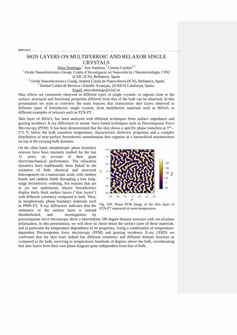
ISAF1-K3-4 _____________________________________________________________________________________________________________________
SKIN LAYERS ON MULTIFERROIC AND RELAXOR SINGLE
CRYSTALS Neus Domingo,
1 Jose Santisso,
1 Gustau Catalan
2,3
1 Oxide Nanoelectronics Group, Centre d’Investigació en Nanociència i Nanotecnologia, CIN2
(CSIC-ICN), Bellaterra, Spain 2 Oxide Nanoelectronics Group, Institut Català de Nanociència (ICN), Bellaterra, Spain
3 Institut Catala de Recerca i Estudis Avançats, (ICREA) Catalunya, Spain.
Email: [email protected]
Skin effects are commonly observed in different types of single crystals: in regions close to the
surface, structural and functional properties different from that of the bulk can be observed. In this
presentation we want to overview the main features that characterize skin layers observed in
different types of ferroelectric single crystals, from multiferroic materials such as BiFeO3 to
different examples of relaxors such as PZN-PT.
Skin layer of BiFeO3 has been analyzed with different techniques from surface impedance and
grazing incidence X-ray diffraction to atomic force based techniques such as Piezoresponse Force
Microscopy (PFM). It has been demonstrated that the skin shows a specific phase transition at T*
275 ºC below the bulk transition temperature, characteristic dielectric properties and a complex
distribution of near-surface ferroelectric nanodomains that organize in a hierarchical metastructure
on top of the existing bulk domains.
On the other hand, morphotropic phase boundary
relaxors have been intensely studied for the last
15 years, on account of their giant
electromechanical performance. The relaxation
dynamics have traditionally been linked to the
existence of both chemical and structural
heterogeneity on a nanoscopic scale, with random
bonds and random fields disrupting a true long-
range ferroelectric ordering. For reasons that are
as yet not understood, relaxor ferroelectrics
display fairly thick surface layers (“skin layers”)
with different symmetry compared to bulk. Thus,
in morphotropic phase boundary materials such
as PMN-PT, X-ray diffraction indicates that the
symmetry of the surface layer is instead
rhombohedral, and investigations by
piezoresponse force microscopy show a labyrinthine 180 degree domain structure with out-of-plane
polarization. In this presentation, we will show in closer detail the surface layer of these materials,
and in particular the temperature dependence of its properties. Using a combination of temperature-
dependent Piezoresponse force microscopy (PFM) and grazing incidence X-ray (XRD) we
confirmed that the skin layer indeed has different symmetry and different domain structure as
compared to the bulk, surviving to temperatures hundreds of degrees above the bulk, corroborating
that skin layers have their own phase diagram quite independent from that of bulk.
Fig. 100: Phase PFM image of the skin layer of
PZN-PT measured at room temperature.
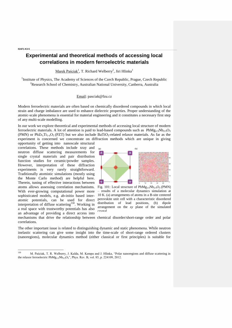
ISAF1-K3-5 _____________________________________________________________________________________________________________________
Experimental and theoretical methods of accessing local
correlations in modern ferroelectric materials
Marek Paściak1, T. Richard Welberry
2, Jiri Hlinka
1
1Institute of Physics, The Academy of Sciences of the Czech Republic, Prague, Czech Republic
2Research School of Chemistry, Australian National University, Canberra, Australia
Email: [email protected]
Modern ferroelectric materials are often based on chemically disordered compounds in which local
strain and charge imbalance are used to enhance dielectric properties. Proper understanding of the
atomic-scale phenomena is essential for material engineering and it constitutes a necessary first step
of any multi-scale modelling.
In our work we explore theoretical and experimental methods of accessing local structure of modern
ferroelectric materials. A lot of attention is paid to lead-based compounds such as PbMg1/3Nb2/3O3
(PMN) or PbZrxTi1-xO3 (PZT) but we also include BaTiO3-related relaxor materials. As far as the
experiment is concerned we concentrate on diffraction methods which are unique in giving
opportunity of getting into nanoscale structural
correlations. These methods include xray and
neutron diffuse scattering measurements for
single crystal materials and pair distribution
function studies for ceramic/powder samples.
However, interpretation of these diffraction
experiments is very rarely straightforward.
Traditionally atomistic simulations (mostly using
the Monte Carlo method) are helpful here.
Therein, tuning of effective interactions between
atoms allows assessing correlation mechanisms.
With ever-growing computational power more
sophisticated models, e.g. ab-initio based inter-
atomic potentials, can be used for direct
interpretation of diffuse scattering330
. Working in
a real space with trustworthy potentials has also
an advantage of providing a direct access into
mechanisms that drive the relationship between chemical disorder/short-range order and polar
correlations.
The other important issue is related to distinguishing dynamic and static phenomena. While neutron
inelastic scattering can give some insight into the time-scale of short-range ordered clusters
(nanoregions), molecular dynamics method (either classical or first principles) is suitable for
330
M. Paściak, T. R. Welberry, J. Kulda, M. Kempa and J. Hlinka, “Polar nanoregions and diffuse scattering in
the relaxor ferroelectric PbMg1/3Nb2/3O3”, Phys. Rev. B, vol. 85, p. 224109, 2012.
Fig. 101: Local structure of PbMg1/3Nb2/3O3 (PMN)
– results of a molecular dynamics simulation at
10 K. (a) arrangements of atoms in a B-site centered
perovskite unit cell with a characteristic disordered
distribution of lead positions, (b) dipole
arrangement on the xy plane of the simulated
crystal.

interpretation of these results. Simulations at varied temperatures can help understanding
development of correlations and slowing down processes across (usually diffuse) phase transitions.
ISAF1-K3-6 _____________________________________________________________________________________________________________________
Spin-Phonon Coupling Role towards Ferroelectricity Rise in
Magnetoelectric Y-Substituted GdMnO3
R. Vilarinho1, A. Almeida
1, P. B. Tavares
2 and J. Agostinho Moreira
1
1IFIMUP and IN-Institute of Nanoscience and Nanotechnology, and Departamento de Física e
Astronomia, Faculdade de Ciências da Universidade do Porto, Porto, Portugal. 2Centro de Química, Universidade de Trás-os-Montes e Alto Douro, Vila Real, Portugal.
Email: [email protected]
Magnetoelectric multiferroics are very interesting materials, as they exhibit ferromagnetism and
ferroelectricity coupled together, opening the possibility of new technological devices. However,
these kinds of materials are very scarce. Among the magnetoelectric compounds, some
orthorhombic rare-earth manganites, with distorted perovskite structures, and general formula
RMnO3, with R = Eu to Dy, are the most studiedxxvi
. In these compounds, ferroelectricity has been
comprehended on the ground of the inverse Dzyaloshinskii-Moriya model, where the modulated
spin ordering induces lattice deformations, yielding electric polarization. In this scope, the interplay
between the magnetic and polar degrees of freedom involves spin-lattice and thus spin-phonon
coupling. Spin-phonon coupling has been studied in several magnetoelectric materials by using both
Raman and infrared spectroscopies and have confirmed the significant role played by the
Dzyaloshinskii-Moriya mechanism in determining their phase diagramsxxvii
. Although an extensive
study, the origin of magnetically induced ferroelectricity is not yet fully understood.
In this work, we present a detailed characterization of magnetic, dielectric and thermodynamic
properties, as well as the study of lattice dynamics at low temperatures of the system Gd1-xYxMnO3,
with x = 0 to 0.4. The substitution of the Gd3+
ion by the smaller Y3+
ion enables us to control the
unit cell distortion, involving a complex set of geometrical changes, where two of them stand-up:
Jahn-Teller and tilt of MnO6 octahedra, occurring alternately in opposite directions along the
crystallographic c-direction, if Pbnm notation is used. These distortions, characterized by the bonds
connecting Mn3+
and octahedral oxygen ions, highly depend on the effective size of the R ion (rR).
The great advantage of this solid solution is that by increasing the substitution ratio only the effect
of geometrical mechanisms, and thus the magnetic exchange integrals, is expected to influence its
phase diagram, enabling to establish the role of spin-phonon coupling in tailoring the nature and
number of different phasesxxviii
.
The magnetoelectric effect is evidenced by the anomalous behavior of the dielectric constant
through the magnetic phase transition. Inversion polarization measurements are in favor for non-
linear polar effects, which yields the emergence of ferroelectricity induced by A-site substitution
and magnetic field. The temperature dependence of the Raman active modes of the MnO6 units has
revealed either a positive or negative shift regarding the pure anharmonic temperature dependence
of the phonon frequency, which can be understood in terms of competitive ferromagnetic and
antiferromagnetic interactions, strongly dependent on Y concentration. The relation between spin-
spin correlation function and anomalous Raman mode frequency behavior is evidenced enabling the
determination of the spin-phonon coupling parameter.

Electrocaloric Materials and Devices
CLUB A
Thursday, July 25 2013, 10:30 am - 12:00 pm
Chair: Stanislav Kamba
Institute of Physics, Academy of Sciences of the Czech Republic
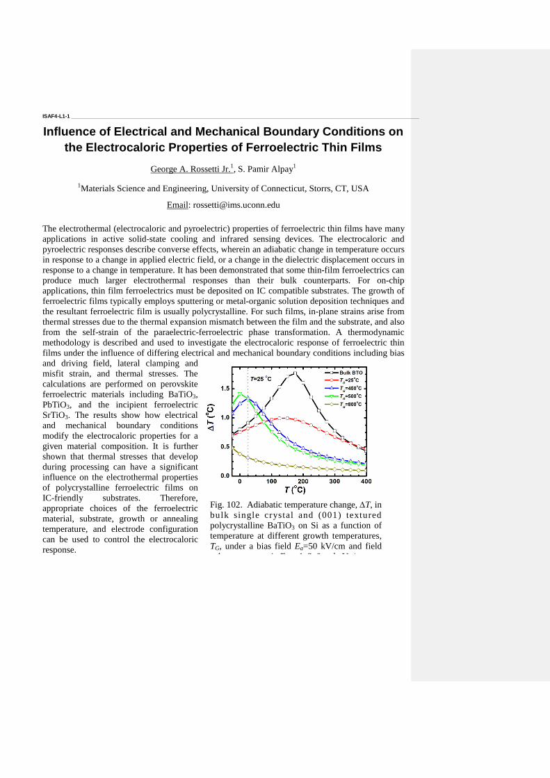
ISAF4-L1-1 _____________________________________________________________________________________________________________________
Influence of Electrical and Mechanical Boundary Conditions on
the Electrocaloric Properties of Ferroelectric Thin Films
George A. Rossetti Jr.1, S. Pamir Alpay
1
1Materials Science and Engineering, University of Connecticut, Storrs, CT, USA
Email: [email protected]
The electrothermal (electrocaloric and pyroelectric) properties of ferroelectric thin films have many
applications in active solid-state cooling and infrared sensing devices. The electrocaloric and
pyroelectric responses describe converse effects, wherein an adiabatic change in temperature occurs
in response to a change in applied electric field, or a change in the dielectric displacement occurs in
response to a change in temperature. It has been demonstrated that some thin-film ferroelectrics can
produce much larger electrothermal responses than their bulk counterparts. For on-chip
applications, thin film ferroelectrics must be deposited on IC compatible substrates. The growth of
ferroelectric films typically employs sputtering or metal-organic solution deposition techniques and
the resultant ferroelectric film is usually polycrystalline. For such films, in-plane strains arise from
thermal stresses due to the thermal expansion mismatch between the film and the substrate, and also
from the self-strain of the paraelectric-ferroelectric phase transformation. A thermodynamic
methodology is described and used to investigate the electrocaloric response of ferroelectric thin
films under the influence of differing electrical and mechanical boundary conditions including bias
and driving field, lateral clamping and
misfit strain, and thermal stresses. The
calculations are performed on perovskite
ferroelectric materials including BaTiO3,
PbTiO3, and the incipient ferroelectric
SrTiO3. The results show how electrical
and mechanical boundary conditions
modify the electrocaloric properties for a
given material composition. It is further
shown that thermal stresses that develop
during processing can have a significant
influence on the electrothermal properties
of polycrystalline ferroelectric films on
IC-friendly substrates. Therefore,
appropriate choices of the ferroelectric
material, substrate, growth or annealing
temperature, and electrode configuration
can be used to control the electrocaloric
response.
Fig. 102. Adiabatic temperature change, T, in
bulk single crystal and (001) textured
polycrystalline BaTiO3 on Si as a function of
temperature at different growth temperatures,
TG, under a bias field Ea=50 kV/cm and field
c h a n g e Δ E = 1 2 0 k V / c m .
ISAF4-L1-2 _____________________________________________________________________________________________________________________
The electrocaloric efficiency of ceramic and polymer films
E.Defay1,2
, S. Crossley2, S. Kar-Narayan
2, X. Moya
2 and N. D. Mathur
2
1CEA, LETI, Minatec Campus, Grenoble, France
2Department of Materials Science, University of Cambridge, Cambridge, UK
Email: [email protected]; [email protected]
Voltage-driven thermal changes known as electrocaloric (EC) effects are large in ferroelectric thin
films near the Curie temperature, where entropic electrical phase transitions may be reversibly
driven by electric fields E that approach the high breakdown fields generically associated with thin
films. The thermal changes in a single film are small, but macroscopic assemblies of ferroelectric
films in the multilayer capacitor geometry have been proposed for cheap, environmentally friendly
and energy efficient cooling applications. However, candidate EC materials have hitherto only been
analysed in terms of EC performance, i.e. the change in isothermal entropy S, the isothermal heat
Q, and the change in adiabatic temperature T. Surprisingly, the corresponding electrical work W
that is done when charging and discharging the host EC capacitors has been neglected. Therefore
we introduce here electrocaloric efficiency to describe the ratio of reversible electrocaloric heat to
reversible electrical work under isothermal conditions1. This figure of merit permits a comparison
of EC materials that does not depend on details of any refrigeration cycle, i.e. the type of cycle, the
hot and cold temperatures of the EC material, and the sink and load temperatures. We investigate in
detail 350 nm thick films of the prototypical electrocaloric ceramic PbZr0.95Ti0.05O3 (PZT) with Pt
electrodes2, and 0.4 - 2.0 µm-thick films of the prototypical electrocaloric polymer poly(vinylidene
fluoride-trifluoroethylene) (55/45 mol %) [P(VDF TrFE)] with Al electrodes3. For these films near
their respective Curie temperatures, the electrical data that were used to predict large and nominally
reversible EC effects, are used here to calculate the nominally reversible electrical work, yielding
= 3.0 for the ceramic and = 7.5 for the polymer. We subsequently use the Landau theory of phase
transitions to reveal the presence of non electrocaloric edge layers that increase the work, and to
reveal the role of a previously observed complexity in the polymer phase transition of ref. 3. In a
wider study, we find that ceramic and polymer films possess overlapping efficiencies, and therefore
both classes of material may be attractive for applications despite previous indications. More
generally, optimising should in future guide the selection of electrocaloric, elastocaloric and
magnetocaloric materials for novel cooling devices that are energy efficient.
1 E. Defay, S. Crossley, S. Kar-Narayan, X. Moya and N. D. Mathur, Adv. Mat., 2013
2 A. S. Mischenko, Q. Zhang, J. F. Scott, R. W. Whatmore and N. D. Mathur, Science, 2006, 311, 1270.
3 B. Neese, B. Chu, S.-G. Lu, Y. Wang, E. Furman and Q. M. Zhang, Science, 2008, 321, 821.
ISAF4-L1-3 _____________________________________________________________________________________________________________________
High Temperature Piezoelectric and Electrocaloric Metrology
P. M. Weaver1, P. Woolliams
1, T. Correia
1, G. Bartl
3, T. Quast
3, T. Stevenson
4, J. Hameury
5, P.
Klapetek6, M. Shpak
7, T. Schmitz-Kempen
8
1National Physical Laboratory, Teddington, UK
2Department, Institution/Company, City, State/Country
3Physikalisch-Technische Bundesanstalt (PTB), Braunschweig, Germany
4Institute for Materials Research, University of Leeds, Leeds, UK
5Laboratoire National de Métrologie et d’Essais (LNE), Trappes / France
6Department, Institution/Company, City, State/Country
7Thermal and Mass Metrology, Centre for Metrology and Accreditation, Espoo, Finland
8aixACCT Systems GmbH, Aachen, Germany
Email: [email protected]
New piezoelectric materials capable of operating at elevated temperatures, are being developed to
reduce energy consumption and improve efficiency and reliability in automotive, energy, process,
electronics and medical industries. Degradation of material and electrical properties at high
temperature means that these applications are typically limited to operating below 200 °C. The
electrocaloric effect in ferroelectrics has strong potential as an efficient cooler for computer chips
and domestic and industrial refrigeration. The ferroelectric materials used in these applications
exhibit strong coupling between electrical, thermal and mechanical properties. Direct coupling
provides the technological useful properties of piezoelectric and electrocaloric effects, but cross-
coupling also needs to be taken into account. Examples include the dependence of thermal expansion
(thermoelastic effect) on electrical conditions, and stress effects on electrocaloric cooling.
This presentation describes a pan-European effort to develop new metrological approaches to the
challenges of measuring multifunctional coupling at temperatures up to 1000 °C. Non-contact
approaches to measuring coupled piezoelectric and thermoelastic strain and direct electrocaloric
measurements are described. To unravel the thermoelastic and electromechanical couplings, PTB
conducts high-accuracy piezoelectric strain measurements within a temperature range from room
temperature to 200°C. This is achieved by full-optical-field multi-wavelength interferometry. To
extend the capabilities of the current setup, a heatable sample environment with high-voltage
functionality is being developed. For aixACCT Systems as an industry partner within this project,
extending the test capabilities of their commercial piezoelectric test systems to high temperatures is a
main focus as well as standardization of piezoelectric testing under temperature and creating stable
reference materials and samples for metrology. Initial results on high TC materials of current
technological interest, based on bismuth ferrite perovskite systems, are described.
This work has been performed in the framework of the joint research project “Metrology of electro-
thermal coupling for new functional materials technology”, which is supported by the European
Metrology Research Programme (EMRP), jointly funded by the EMRP participating countries
within EURAMET and the European Union.
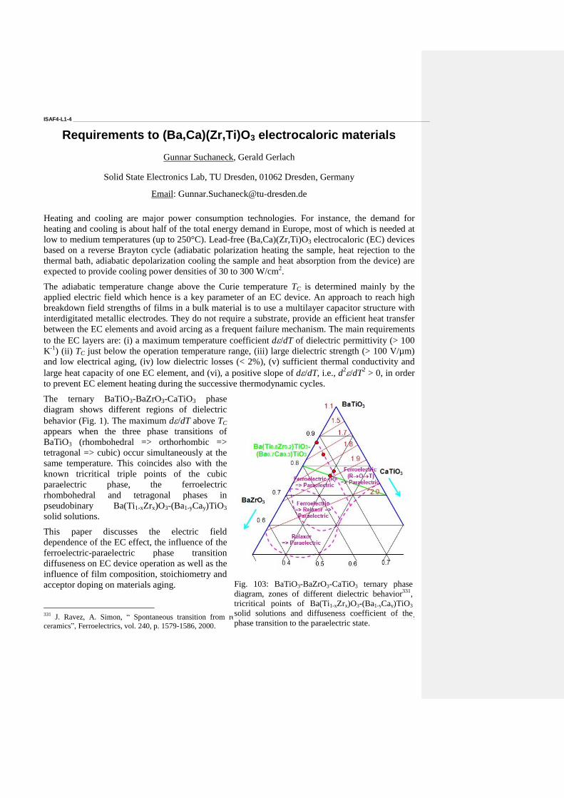
ISAF4-L1-4 _____________________________________________________________________________________________________________________
Requirements to (Ba,Ca)(Zr,Ti)O3 electrocaloric materials
Gunnar Suchaneck, Gerald Gerlach
Solid State Electronics Lab, TU Dresden, 01062 Dresden, Germany
Email: [email protected]
Heating and cooling are major power consumption technologies. For instance, the demand for
heating and cooling is about half of the total energy demand in Europe, most of which is needed at
low to medium temperatures (up to 250°C). Lead-free (Ba,Ca)(Zr,Ti)O3 electrocaloric (EC) devices
based on a reverse Brayton cycle (adiabatic polarization heating the sample, heat rejection to the
thermal bath, adiabatic depolarization cooling the sample and heat absorption from the device) are
expected to provide cooling power densities of 30 to 300 W/cm2.
The adiabatic temperature change above the Curie temperature TC is determined mainly by the
applied electric field which hence is a key parameter of an EC device. An approach to reach high
breakdown field strengths of films in a bulk material is to use a multilayer capacitor structure with
interdigitated metallic electrodes. They do not require a substrate, provide an efficient heat transfer
between the EC elements and avoid arcing as a frequent failure mechanism. The main requirements
to the EC layers are: (i) a maximum temperature coefficient d/dT of dielectric permittivity (> 100
K-1
) (ii) TC just below the operation temperature range, (iii) large dielectric strength (> 100 V/µm)
and low electrical aging, (iv) low dielectric losses (< 2%), (v) sufficient thermal conductivity and
large heat capacity of one EC element, and (vi), a positive slope of d/dT, i.e., d2/dT
2 > 0, in order
to prevent EC element heating during the successive thermodynamic cycles.
The ternary BaTiO3-BaZrO3-CaTiO3 phase
diagram shows different regions of dielectric
behavior (Fig. 1). The maximum d/dT above TC
appears when the three phase transitions of
BaTiO3 (rhombohedral => orthorhombic =>
tetragonal => cubic) occur simultaneously at the
same temperature. This coincides also with the
known tricritical triple points of the cubic
paraelectric phase, the ferroelectric
rhombohedral and tetragonal phases in
pseudobinary Ba(Ti1-xZrx)O3-(Ba1-yCay)TiO3
solid solutions.
This paper discusses the electric field
dependence of the EC effect, the influence of the
ferroelectric-paraelectric phase transition
diffuseness on EC device operation as well as the
influence of film composition, stoichiometry and
acceptor doping on materials aging.
331
J. Ravez, A. Simon, “ Spontaneous transition from relaxor to ferroelectric state in new lead-free perovskite
ceramics”, Ferroelectrics, vol. 240, p. 1579-1586, 2000.
Fig. 103: BaTiO3-BaZrO3-CaTiO3 ternary phase
diagram, zones of different dielectric behavior331
,
tricritical points of Ba(Ti1-xZrx)O3-(Ba1-yCay)TiO3
solid solutions and diffuseness coefficient of the
phase transition to the paraelectric state.

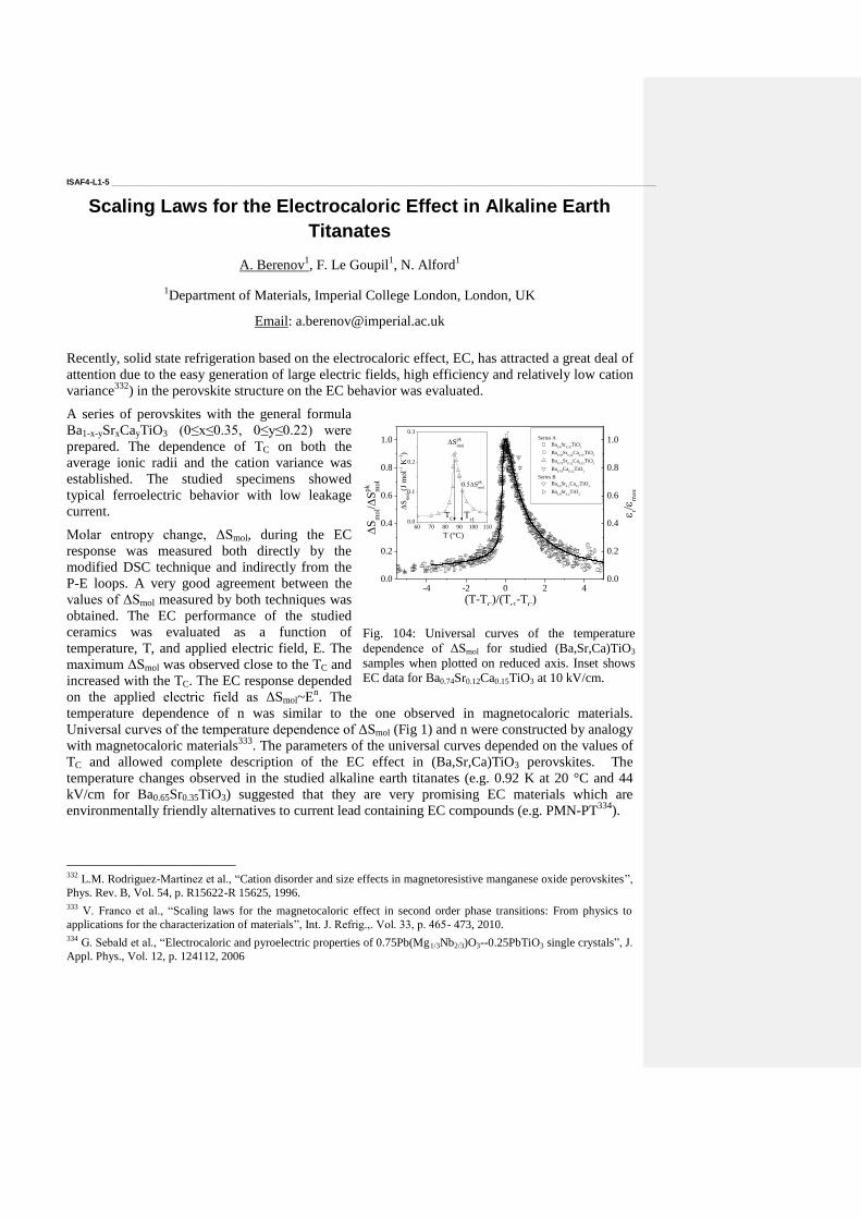
ISAF4-L1-5 _____________________________________________________________________________________________________________________
Scaling Laws for the Electrocaloric Effect in Alkaline Earth
Titanates
A. Berenov1, F. Le Goupil
1, N. Alford
1
1Department of Materials, Imperial College London, London, UK
Email: [email protected]
Recently, solid state refrigeration based on the electrocaloric effect, EC, has attracted a great deal of
attention due to the easy generation of large electric fields, high efficiency and relatively low cation
variance332
) in the perovskite structure on the EC behavior was evaluated.
A series of perovskites with the general formula
Ba1-x-ySrxCayTiO3 (0≤x≤0.35, 0≤y≤0.22) were
prepared. The dependence of TC on both the
average ionic radii and the cation variance was
established. The studied specimens showed
typical ferroelectric behavior with low leakage
current.
Molar entropy change, ΔSmol, during the EC
response was measured both directly by the
modified DSC technique and indirectly from the
P-E loops. A very good agreement between the
values of ΔSmol measured by both techniques was
obtained. The EC performance of the studied
ceramics was evaluated as a function of
temperature, T, and applied electric field, E. The
maximum ΔSmol was observed close to the TC and
increased with the TC. The EC response depended
on the applied electric field as ΔSmol~En. The
temperature dependence of n was similar to the one observed in magnetocaloric materials.
Universal curves of the temperature dependence of ΔSmol (Fig 1) and n were constructed by analogy
with magnetocaloric materials333
. The parameters of the universal curves depended on the values of
TC and allowed complete description of the EC effect in (Ba,Sr,Ca)TiO3 perovskites. The
temperature changes observed in the studied alkaline earth titanates (e.g. 0.92 K at 20 °C and 44
kV/cm for Ba0.65Sr0.35TiO3) suggested that they are very promising EC materials which are
environmentally friendly alternatives to current lead containing EC compounds (e.g. PMN-PT334
).
332
L.M. Rodriguez-Martinez et al., “Cation disorder and size effects in magnetoresistive manganese oxide perovskites”,
Phys. Rev. B, Vol. 54, p. R15622-R 15625, 1996. 333
V. Franco et al., “Scaling laws for the magnetocaloric effect in second order phase transitions: From physics to
applications for the characterization of materials”, Int. J. Refrig.,. Vol. 33, p. 465- 473, 2010. 334
G. Sebald et al., “Electrocaloric and pyroelectric properties of 0.75Pb(Mg1/3Nb2/3)O3--0.25PbTiO3 single crystals”, J.
Appl. Phys., Vol. 12, p. 124112, 2006
-4 -2 0 2 40.0
0.2
0.4
0.6
0.8
1.0 Series A
Ba0.6
Sr0.35
TiO3
Ba0.69
Sr0.24
Ca0.07
TiO3
Ba0.74
Sr0.12
Ca0.15
TiO3
Ba0.78
Ca0.22
TiO3
Series B
Ba0.6
Sr0.2
Ca0.2
TiO3
Ba0.8
Sr0.2
TiO3
S
mo
l/S
pk
mo
l
(T-TC)/(T
r1-T
C)
60 70 80 90 100 1100.0
0.1
0.2
0.3
Spk
mol
S
mo
l (J
mol-1
K-1
)
T (°C)
Spk
mol
TC
Tr1
0.0
0.2
0.4
0.6
0.8
1.0
r/ m
ax
Fig. 104: Universal curves of the temperature
dependence of ΔSmol for studied (Ba,Sr,Ca)TiO3
samples when plotted on reduced axis. Inset shows
EC data for Ba0.74Sr0.12Ca0.15TiO3 at 10 kV/cm.

Modeling: LGD, Phase-Field,...
CLUB B
Thursday, July 25 2013, 10:30 am - 12:00 pm
Chair: To Be Announced
ISAF1-L2-1 _____________________________________________________________________________________________________________________
Thermodynamic Theory and Phase Field Model of Domain
Structures in Ferroelectric Thin Layers and Bi-Layers
Andrei Artemev1 and Alexander Roytburd
2
1Department of Mechanical and Aerospace Engineering, Carleton University, Ottawa, Canada
2Department of Materials Science and Engineering, University of Maryland, College Park, USA
Email: [email protected]
The domain structure in ferroelectric thin layers and bi-layer films formed by weak and strong
ferroelectrics or by a ferroelectric and a dielectric was studied using the homogenized
thermodynamics model and phase field simulations. The thermodynamic analysis predicted that the
increase in the weak ferroelectric or dielectric layer thickness would result in the changes in the
critical field of the single-domain (SD) to polydomain (PD) transition from negative to positive, and
the hysteresis loop shape from simple rectangular to composite, consisting of two offset triangular
loops describing the PD↔SD transition hysteresis and a central loop describing the hysteresis of the
PD state switching, with the central loop reduced to a zero-hysteresis P(E) curve in dielectric-
ferroelectric bilayers, and in the reduction in the remnant polarization and coercive field.
The phase field simulations were performed for the a) bilayers consisting of either strong
ferroelectric BaTiO3 and weak ferroelectric Ba0.3Sr(1-0.3)TiO3 or strong ferroelectric BaTiO3 and
dielectric Ba0.2Sr(1-0.2)TiO3 with a high dielectric constant (=950), and b) thin layers of BaTiO3 with
a low dielectric constant (=8) deadlayers. In all simulations the clamping effect of the SrTiO3
substrate was introduced using the renormalization of the Landau-Ginsburg-Devonshire free energy
density function. The simulations were performed for the bilayers with different a) ratios of the
layer thickness and b) absolute thickness of the BaTiO3 ferroelectric layer. In all simulations the
clamping effect of the substrate resulted in the 180o domain structure formation. 1D and 3D
ferroelectric models produced significantly different results; hence, it is important to use a full 3D
ferroelectric model even for the simulation of films containing only 180o c domains due to clamping
or poling effects.
The phase field simulations demonstrated that the stripe (or labyrinth) domain structure is produced
in all films by the transformation from a paraelectric state at zero applied field conditions. The
domain structure completely penetrates a weak ferroelectric or dielectric layer with a high dielectric
constant; however, there is almost no penetration into low dielectric constant deadlayers. This
domain structure transforms into columnar domains during poling, after which the PD state changes
into the SD state. The P(E) loops obtained by the phase field modeling for strong ferroelectric-weak
ferroelectric bilayers were similar to those predicted by the thermodynamic model. However, the
loops obtained for strong ferroelectric - dielectric bilayers differed from the thermodynamic
predictions. As a result of a specific behavior of the columnar domain structure produced by the SD
to PD transition in the reversing applied field, they had a central loop with a large hysteresis effect
instead of a zero-hysteresis curve connecting two offset triangular loops. Phase field modeling
demonstrated the possibility of the hysteresis effect of the stripe to columnar domain morphology
transition appearing as a result of a repulsive interaction between columnar domains. The
simulation results and thermodynamic analysis demonstrate that in thin films the SD to PD

transition can go through the spinodal decomposition of the SD state, while in thick films it should
develop by the nucleation and growth mechanism.
ISAF1-L2-2 _____________________________________________________________________________________________________________________
Tracking the origin of dielectric response of simple domain
patterns in BaTiO3
P. Marton, I. Rychetský, A. Klíč, and J. Hlinka
Department of dielectrics, Institute of Physics, Acad. Sci. Czech Rep., Praha, Czech Republic
Email: [email protected]
Domain walls in ferroelectric materials are known to have significant impact on the
electromechanical response to an external loading. The exact role of domain walls in dielectric
response is, nevertheless, complex and not yet fully understood. A domain wall can sweep
macroscopically through the crystal, allowing polarization reversal at moderate electric-field
amplitudes well below the coercive field of a monodomain sample. In reality, however, the mobility
of walls is usually strongly limited, e.g. due to different types of pinning.
Even if macroscopically immobile, walls can still significantly alter the dielectric response. The
effect may originate e.g. in domain-wall deflection from its original position, broadening, and other
recently suggested mechanisms335336337338
. There are as well simple situations where a domain wall
only acts as an interface between the surrounding domains, and the domain geometry itself and its
relation to the acting field are dominant.
In this contribution we provide analysis of a frequency-dependent dielectric response of several
important domain patterns appearing in the tetragonal phase of prototype ferroelectric material
BaTiO3. We make distinction between the response from a domain wall, and response from domain
structure as such. Combination of the analytical algebraic derivations and numerical simulations
within the Ginzburg-Landau-Devonshire phenomenological theory, complemented with the Finite-
element-method339
simulations of domain configuration with zero-thickness domain walls is
employed.
335
Rao and Wang, “Domain wall broadening mechanism for domain size effect of enhanced piezoelectricity in
crystallographically engineered ferroelectric single crystals ” Appl. Phys. Lett., vol. 90, p. 041915, 2007. 336
J. Hlinka, P. Ondrejkovic, and P. Marton, “The piezoelectric response of nanotwinned BaTiO3 ”, Nanotechnology, vol. 20, p. 105709 , 2009. 337
V. Stepkova, P. Marton, and J. Hlinka, ”Stress-induced phase transition in
ferroelectric domain walls of BaTiO3”, J. Phys.: Condens. Matter, vol. 24, p. 212201, 2013. 338
T. Sluka, A. K. Taganstev, D. Damjanovic, M. Gureev, and N. Setter, “Enhanced electromechanical response
of ferroelectrics due to charged domain walls”, Nature Communications, vol. 3, p. 748, 2012. 339
A. Klic and I. Rychetsky, “Dielectric Response of Arbitrary-Shaped Clusters Studied by the Finite Element
Method”, Ferroelectrics, vol. 427, p. 143, 2012.
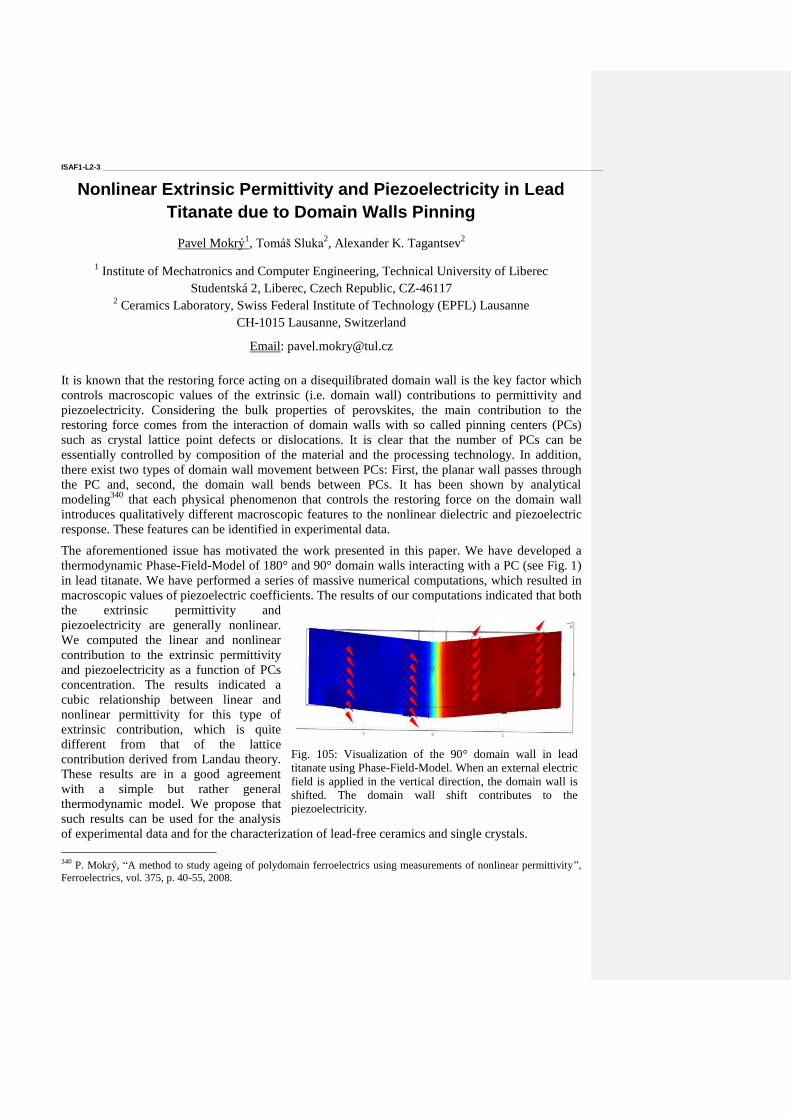
ISAF1-L2-3 _____________________________________________________________________________________________________________________
Nonlinear Extrinsic Permittivity and Piezoelectricity in Lead
Titanate due to Domain Walls Pinning
Pavel Mokrý1, Tomáš Sluka
2, Alexander K. Tagantsev
2
1 Institute of Mechatronics and Computer Engineering, Technical University of Liberec
Studentská 2, Liberec, Czech Republic, CZ-46117 2 Ceramics Laboratory, Swiss Federal Institute of Technology (EPFL) Lausanne
CH-1015 Lausanne, Switzerland
Email: [email protected]
It is known that the restoring force acting on a disequilibrated domain wall is the key factor which
controls macroscopic values of the extrinsic (i.e. domain wall) contributions to permittivity and
piezoelectricity. Considering the bulk properties of perovskites, the main contribution to the
restoring force comes from the interaction of domain walls with so called pinning centers (PCs)
such as crystal lattice point defects or dislocations. It is clear that the number of PCs can be
essentially controlled by composition of the material and the processing technology. In addition,
there exist two types of domain wall movement between PCs: First, the planar wall passes through
the PC and, second, the domain wall bends between PCs. It has been shown by analytical
modeling340
that each physical phenomenon that controls the restoring force on the domain wall
introduces qualitatively different macroscopic features to the nonlinear dielectric and piezoelectric
response. These features can be identified in experimental data.
The aforementioned issue has motivated the work presented in this paper. We have developed a
thermodynamic Phase-Field-Model of 180° and 90° domain walls interacting with a PC (see Fig. 1)
in lead titanate. We have performed a series of massive numerical computations, which resulted in
macroscopic values of piezoelectric coefficients. The results of our computations indicated that both
the extrinsic permittivity and
piezoelectricity are generally nonlinear.
We computed the linear and nonlinear
contribution to the extrinsic permittivity
and piezoelectricity as a function of PCs
concentration. The results indicated a
cubic relationship between linear and
nonlinear permittivity for this type of
extrinsic contribution, which is quite
different from that of the lattice
contribution derived from Landau theory.
These results are in a good agreement
with a simple but rather general
thermodynamic model. We propose that
such results can be used for the analysis
of experimental data and for the characterization of lead-free ceramics and single crystals.
340
P. Mokrý, “A method to study ageing of polydomain ferroelectrics using measurements of nonlinear permittivity”,
Ferroelectrics, vol. 375, p. 40-55, 2008.
Fig. 105: Visualization of the 90° domain wall in lead
titanate using Phase-Field-Model. When an external electric
field is applied in the vertical direction, the domain wall is
shifted. The domain wall shift contributes to the
piezoelectricity.

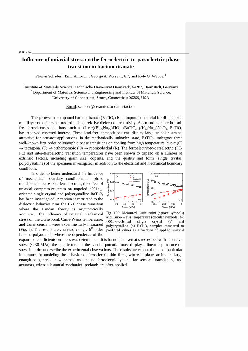
ISAF1-L2-4 _____________________________________________________________________________________________________________________
Influence of uniaxial stress on the ferroelectric-to-paraelectric phase
transition in barium titanate
Florian Schader1, Emil Aulbach
1, George A. Rossetti, Jr.
2, and Kyle G. Webber
1
1Institute of Materials Science, Technische Universität Darmstadt, 64287, Darmstadt, Germany
2 Department of Materials Science and Engineering and Institute of Materials Science,
University of Connecticut, Storrs, Connecticut 06269, USA
Email: [email protected]
The perovskite compound barium titanate (BaTiO3) is an important material for discrete and
multilayer capacitors because of its high relative dielectric permittivity. As an end member in lead-
free ferroelectrics solutions, such as (1-x-y)(Bi1/2Na1/2)TiO3–xBaTiO3–y(K0.5Na0.5)NbO3, BaTiO3
has received renewed interest. These lead-free compositions can display large unipolar strains,
attractive for actuator applications. In the mechanically unloaded state, BaTiO3 undergoes three
well-known first order polymorphic phase transitions on cooling from high temperature, cubic (C)
tetragonal (T) orthorhombic (O) rhombohedral (R). The ferroelectric-to-paraelectric (FE-
PE) and inter-ferroelectric transition temperatures have been shown to depend on a number of
extrinsic factors, including grain size, dopants, and the quality and form (single crystal,
polycrystalline) of the specimen investigated, in addition to the electrical and mechanical boundary
conditions.
In order to better understand the influence
of mechanical boundary conditions on phase
transitions in perovskite ferroelectrics, the effect of
uniaxial compressive stress on unpoled <001>C-
oriented single crystal and polycrystalline BaTiO3
has been investigated. Attention is restricted to the
dielectric behavior near the C-T phase transition
where the Landau theory is asymptotically
accurate. The influence of uniaxial mechanical
stress on the Curie point, Curie-Weiss temperature,
and Curie constant were experimentally measured
(Fig. 1). The results are analyzed using a 6th
order
Landau polynomial, where the dependence of the
expansion coefficients on stress was determined. It is found that even at stresses below the coercive
stress (< 30 MPa), the quartic term in the Landau potential must display a linear dependence on
stress in order to describe the experimental observations. The results are expected to be of particular
importance in modeling the behavior of ferroelectric thin films, where in-plane strains are large
enough to generate new phases and induce ferroelectricity, and for sensors, transducers, and
actuators, where substantial mechanical preloads are often applied.
Fig. 106: Measured Curie point (square symbols)
and Curie-Weiss temperature (circular symbols) for
<001>C-oriented single crystal (a) and
polycrystalline (b) BaTiO3 samples compared to
predicted values as a function of applied uniaxial
compressive stress.
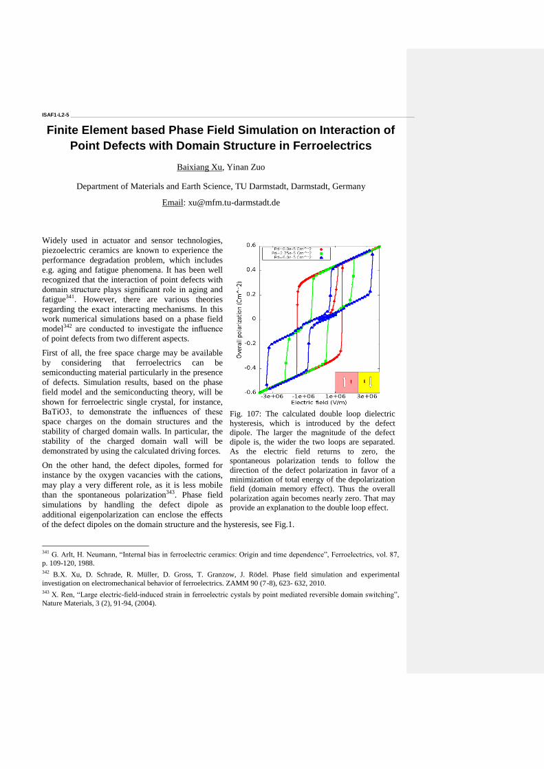
ISAF1-L2-5 _____________________________________________________________________________________________________________________
Finite Element based Phase Field Simulation on Interaction of
Point Defects with Domain Structure in Ferroelectrics
Baixiang Xu, Yinan Zuo
Department of Materials and Earth Science, TU Darmstadt, Darmstadt, Germany
Email: [email protected]
Widely used in actuator and sensor technologies,
piezoelectric ceramics are known to experience the
performance degradation problem, which includes
e.g. aging and fatigue phenomena. It has been well
recognized that the interaction of point defects with
domain structure plays significant role in aging and
fatigue341. However, there are various theories
regarding the exact interacting mechanisms. In this
work numerical simulations based on a phase field
model342 are conducted to investigate the influence
of point defects from two different aspects.
First of all, the free space charge may be available
by considering that ferroelectrics can be
semiconducting material particularly in the presence
of defects. Simulation results, based on the phase
field model and the semiconducting theory, will be
shown for ferroelectric single crystal, for instance,
BaTiO3, to demonstrate the influences of these
space charges on the domain structures and the
stability of charged domain walls. In particular, the
stability of the charged domain wall will be
demonstrated by using the calculated driving forces.
On the other hand, the defect dipoles, formed for
instance by the oxygen vacancies with the cations,
may play a very different role, as it is less mobile
than the spontaneous polarization343. Phase field
simulations by handling the defect dipole as
additional eigenpolarization can enclose the effects
of the defect dipoles on the domain structure and the hysteresis, see Fig.1.
341
G. Arlt, H. Neumann, “Internal bias in ferroelectric ceramics: Origin and time dependence”, Ferroelectrics, vol. 87,
p. 109-120, 1988. 342
B.X. Xu, D. Schrade, R. Müller, D. Gross, T. Granzow, J. Rödel. Phase field simulation and experimental
investigation on electromechanical behavior of ferroelectrics. ZAMM 90 (7-8), 623- 632, 2010. 343
X. Ren, “Large electric-field-induced strain in ferroelectric cystals by point mediated reversible domain switching”,
Nature Materials, 3 (2), 91-94, (2004).
Fig. 107: The calculated double loop dielectric
hysteresis, which is introduced by the defect
dipole. The larger the magnitude of the defect
dipole is, the wider the two loops are separated.
As the electric field returns to zero, the
spontaneous polarization tends to follow the
direction of the defect polarization in favor of a
minimization of total energy of the depolarization
field (domain memory effect). Thus the overall
polarization again becomes nearly zero. That may
provide an explanation to the double loop effect.

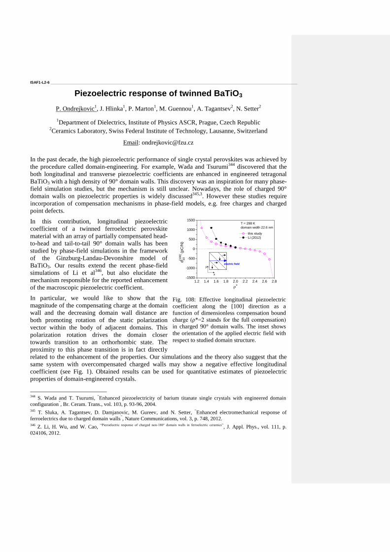
ISAF1-L2-6 _____________________________________________________________________________________________________________________
Piezoelectric response of twinned BaTiO3
P. Ondrejkovic1, J. Hlinka
1, P. Marton
1, M. Guennou
1, A. Tagantsev
2, N. Setter
2
1Department of Dielectrics, Institute of Physics ASCR, Prague, Czech Republic
2Ceramics Laboratory, Swiss Federal Institute of Technology, Lausanne, Switzerland
Email: [email protected]
In the past decade, the high piezoelectric performance of single crystal perovskites was achieved by
the procedure called domain-engineering. For example, Wada and Tsurumi344
discovered that the
both longitudinal and transverse piezoelectric coefficients are enhanced in engineered tetragonal
BaTiO3 with a high density of 90° domain walls. This discovery was an inspiration for many phase-
field simulation studies, but the mechanism is still unclear. Nowadays, the role of charged 90°
domain walls on piezoelectric properties is widely discussed345,3
. However these studies require
incorporation of compensation mechanisms in phase-field models, e.g. free charges and charged
point defects.
In this contribution, longitudinal piezoelectric
coefficient of a twinned ferroelectric perovskite
material with an array of partially compensated head-
to-head and tail-to-tail 90° domain walls has been
studied by phase-field simulations in the framework
of the Ginzburg-Landau-Devonshire model of
BaTiO3. Our results extend the recent phase-field
simulations of Li et al346
, but also elucidate the
mechanism responsible for the reported enhancement
of the macroscopic piezoelectric coefficient.
In particular, we would like to show that the
magnitude of the compensating charge at the domain
wall and the decreasing domain wall distance are
both promoting rotation of the static polarization
vector within the body of adjacent domains. This
polarization rotation drives the domain closer
towards transition to an orthorhombic state. The
proximity to this phase transition is in fact directly
related to the enhancement of the properties. Our simulations and the theory also suggest that the
same system with overcompensated charged walls may show a negative effective longitudinal
coefficient (see Fig. 1). Obtained results can be used for quantitative estimates of piezoelectric
properties of domain-engineered crystals.
344
S. Wada and T. Tsurumi, “Enhanced piezoelectricity of barium titanate single crystals with engineered domain
configuration”, Br. Ceram. Trans., vol. 103, p. 93-96, 2004.
345 T. Sluka, A. Tagantsev, D. Damjanovic, M. Gureev, and N. Setter,
“Enhanced electromechanical response of
ferroelectrics due to charged domain walls”, Nature Communications, vol. 3, p. 748, 2012.
346 Z. Li, H. Wu, and W. Cao,
“Piezoelectric response of charged non-180° domain walls in ferroelectric ceramics”, J. Appl. Phys., vol. 111, p.
024106, 2012.
1.2 1.4 1.6 1.8 2.0 2.2 2.4 2.6 2.8-1500
-1000
-500
0
500
1000
1500
d[1
00]
33
(pC
/N)
*
this study
Li (2012)
T = 298 K
domain width 22.6 nm
x
yelectric field
Fig. 108: Effective longitudinal piezoelectric
coefficient along the [100] direction as a
function of dimensionless compensation bound
charge (ρ*=2 stands for the full compensation)
in charged 90° domain walls. The inset shows
the orientation of the applied electric field with
respect to studied domain structure.

Les Bowen Memorial Session on Transducer Materials and Devices
CLUB C
Thursday, July 25 2013, 10:30 am - 12:00 pm
Chair: Ahmad Safari
Rutgers University
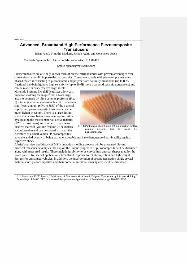
ISAF4-L3-1 _____________________________________________________________________________________________________________________
Advanced, Broadband High Performance Piezocomposite Transducers
Brian Pazol, Timothy Mudarri, Joseph Aghia and Constance Ursch
Materials Systems Inc., Littleton, Massachusetts, USA 01460
Email: [email protected]
Piezocomposites are a widely known form of piezoelectric material with proven advantages over
conventional monolithic piezoelectric ceramics. Transducers made with piezocomposite (a two
phased material consisting of piezoceramic and polymer) are naturally broadband (up to 80%
fractional bandwidth), have high sensitivity (up to 10 dB more than solid ceramic transducers) and
can be made in cost effective large sheets.
Materials Systems Inc. (MSI) utilizes a low cost
injection molding technique1 that allows large
areas to be made by tiling ceramic preforms (Fig.
1) into large areas at a reasonable cost. Because a
significant amount (60% to 85%) of the material
is polymer, piezocomposite transducers can be
much lighter in weight. There is a large design
space that allows better transducer optimization
by adjusting the matrix material, active material
(PZT in most cases) and the ratio of active to
inactive material (volume fraction). The material
is conformable and can be shaped to match the
curvature of a small vehicle. Piezocomposites
have the added benefit of being extremely durable and have demonstrated survivability against
explosive shock.
A brief overview and history of MSI’s injection molding process will be presented. Several
practical transducer examples that exploit the unique properties of piezocomposite will be discussed
along with measured results. These include its ability to be curved into unusual shapes to tailor the
beam pattern for special applications, broadband response for clutter rejection and lightweight
designs for unmanned vehicles. In addition, the incorporation of second generation single crystal
materials into piezocomposites and their potential in future sonar systems will be discussed.
1 L. J. Bowen and K. W. French, “Fabrication of Piezocomposite Ceramic/Polymer Composites by Injection Molding,”
Proceedings of the 8th
IEEE International Symposium on Applications of Ferroelectrics, pp. 160-163, 1992.
Fig. 1: Photograph of a 50 mm x 50 mm injection molded
ceramic preform used to make 1-3
piezocomposite.
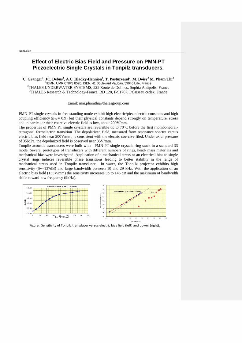
ISAF4-L3-2 _____________________________________________________________________________________________________________________
Effect of Electric Bias Field and Pressure on PMN-PT Piezoelectric Single Crystals in Tonpilz transducers.
C. Granger
1, JC. Debus
1, A.C. Hladky-Hennion
1, T. Pastureaud
2, M. Doisy
2 M. Pham Thi
3
1IEMN, UMR CNRS 8520, ISEN, 41 Boulevard Vauban, 59046 Lille, France
2THALES UNDERWATER SYSTEMS, 525 Route de Dolines, Sophia Antipolis, France 3THALES Research & Technology-France, RD 128, F-91767, Palaiseau cedex, France
Email: [email protected]
PMN-PT single crystals in free standing mode exhibit high electric/piezoelectric constants and high
coupling efficiency (k33 = 0.9) but their physical constants depend strongly on temperature, stress
and in particular their coercive electric field is low, about 200V/mm.
The properties of PMN PT single crystals are reversible up to 70°C before the first rhombohedral-
tetragonal ferroelectric transition. The depolarized field, measured from resonance spectra versus
electric bias field near 200V/mm, is consistent with the electric coercive filed. Under axial pressure
of 35MPa, the depolarized field is observed near 35V/mm.
Tonpilz acoustic transducers were built with PMN-PT single crystals ring stack in a standard 33
mode. Several prototypes of transducers with different numbers of rings, head- mass materials and
mechanical bias were investigated. Application of a mechanical stress or an electrical bias to single
crystal rings induces reversible phase transitions leading to better stability in the range of
mechanical stress used in Tonpilz transducer. In water, the Tonpilz projector exhibits high
sensitivity (Sv=137dB) and large bandwidth between 10 and 29 kHz. With the application of an
electric bias field (135V/mm) the sensitivity increases up to 145 dB and the maximum of bandwidth
shifts toward low frequency (9kHz).
Figure: Sensitivity of Tonpilz transducer versus electric bias field (left) and power (right).
ISAF4-L3-3 _____________________________________________________________________________________________________________________
Flextensional Composite Structure with PZN-PZT Crystals for
Energy Harvesting Applications
Emre Tufekcioglu1, Aydin Dogan
1
1Department of Materials Science and Engineering
Faculty of Engineering
Anadolu University, 26555, Eskisehir, TURKEY
Email: [email protected]
The majority of piezoelectric energy harvesting research is based on structures operating in 31
(transverse) mode. For obtaining the highest level of energy from 31 mode, energy harvesters are
constructed to produce the maximum strain on the transducer material, i.e. the bimorph transducers
or monomorph patches adhered on beams. The high level of cyclic tensile stresses applied on the
piezoelectric ceramic materials cause microcracks to form inside the material and eventually failure
occurs.
In this study, the power harvesting capability of a flextensional piezo-composite structure with
PZN-PZT relaxor-ferroelectric crystals as electro-active materials was evaluated. The flextensional
piezo-composite is constantly kept under pre-stress so that the life-time of the ceramic is extended.
The energy harvesting (EH) structure consists of a cymbal electromechanical transducer and an
attached proof mass, all pre-stressed inside a rigid frame (Fig. 1). The power harvested was
evaluated by vibrating the whole structure sinusoidally with varying frequencies and measuring the
electrical outputs like voltage, current and power depending on the frequency, pre-stress, proof
mass and resistive load. The results obtained from the PZN-PZT crystals were compared with the
results obtained from soft PZT crystals.
Results show that the PH structure with PZN-PZT crystals is capable of producing 700 μW of
power at 4300 Hz and with a 5N of prestress which was measured across an electrical resistance of
100 kΩ. The measured power is more than two times the power generated by the structure with soft
PZT crystals.

Fig. 1. The Energy Harvesting Structure
ISAF4-L3-4 _____________________________________________________________________________________________________________________
Effect of Growth Conditions on Performance of
0.67BiFeO3-0.33BaTiO3 Bulk Acoustic Wave Resonators
Andrei Vorobiev1, Spartak Gevorgian
1, Markus Löffler
2, Eva Olsson
2
1Department of Microtechnology and Nanoscience, Chalmers University of Technology,
Gothenburg, Sweden 2Department Applied Physics, Chalmers University of Technology, Gothenburg, Sweden
Email: [email protected]
Intrinsically tunable 0.67BiFeO3-0.33BaTiO3 (BF-BT) thin film bulk acoustic wave resonators with
record high tunability of 4.4%, electromechanical coupling coefficient of 10% and rather high Q-
factor of 200, at 4 GHz, have been demonstrated recently347
. In the proposed contribution we
disclose, for the first time, results of comprehensive studies of correlations between the growth
conditions, microstructure and acoustic performance of the resonators, which allowed for
optimization of the growth condition and achieving the device high performance. Particularly, it is
shown that the pulsed laser deposition results in a strong asymmetric distribution of the BF-BT film
grain size, surface roughness and texturing. The rms surface roughness decreases, from 30 nm to
12 nm in the beam-plume plane, leading to significant increase in the Q-factor, from 20 up to 200
(Fig. 1), due to reduction of loss associated with
wave scattering at reflection from rough interface.
We explain the phenomenon by an asymmetric
angular energy distribution of the plume species
caused by the laser beam-plume interaction.
The BF-BT film microstructure and surface
morphology are analyzed by means of XRD,
SEM, TEM and AFM. The observed distribution
of the surface roughness is associated with
variations in the lateral grain size and shape of the
grain faceted tips due to the BF-BT film texturing.
The films grown in the area affected by the beam-
plume interaction are more (100) oriented in
comparison with the on-axis films revealing more
(110) grains.
The tunable performance of the BF-BT resonators
is analyzed using the theory of dc field induced piezoelectric effect. The increase in the
electromechanical coupling coefficient, from 6% to 10%, for the (100) oriented films, is associated
with anisotropy of the linear electrostriction coefficient. Analysis of tunabilty of the parallel
resonance frequency indicates also anisotropy of the nonlinear electrostriction coefficient. The
higher and negative nonlinear electrostriction coefficient of the (100) oriented films limits the
tunabilty of the series resonance frequency.
347
A. Vorobiev, S. Gevorgian, N. Martirisyan, M. Löffler, and E. Olsson “Intrinsically tunable
0.67BiFeO3-0.33BaTiO3 thin film bulk acoustic wave resonators”, Appl. Phys. Lett., vol. 101, p. 232903 -5, 2012.
Fig. 109: Q-factors of the resonators with BF-BT
films grown in different positions relative to the
laser plume axis. Corresponding rms surface
roughness is given in brackets.

We assume that the observed effect of the laser beam-plume interaction is general and should be
taken into account for any type of perovskite films grown by the pulsed laser deposition.
ISAF4-L3-5 _____________________________________________________________________________________________________________________
Hysteresis-Free High-Temperature Bimorph Lithium Niobate
Actuators Produced by Direct Bonding
Zorikhin Dmitry1,2
, Baturin Ivan1,2
, Mingaliev Eugene1,2
, Udalov Artur1,
Akhmatkhanov Andrey1,2
, Zelenovskiy Pavel1, Shur Vladimir
1,2
1Ferroelectric Laboratory, Ural Federal University, Ekaterinburg, Russia
2Labfer Ltd., Ekaterinburg, Russia
Email: [email protected]
Piezoelectric materials are widely used for precise positioning systems. Conventional piezoelectric materials such as PZT and lead-free ceramics have high piezoelectric coefficients but lack the temperature stability due to low Curie temperature (Tc) and are prone to hysteresis and nonlinear behavior. The manufacturing of linear hysteresis-free piezoelectric actuators operable in a wide temperature range (from 77 to 900K) presents an actual technical challenge. Lithium niobate LiNbO3 (LN) single crystals can be used in a wide temperature range (Tc = 1200
oC). Bimorph
bending actuators based on bidomain LN crystals were realized by annealing close to Tc which leads to formation of domain wall in the middle of the wafer
xxix,xxx. Present work is focused on the
fabrication of bimorph LN actuators using wafer-scale direct bonding.
Based on the angular dependence of the piezoelectric coefficients the optimal wafer orientations for bimorph layers were selected. Commercially available wafers with Y+128° and Y+41° (rotation of Y+ axis towards Z+) cuts characterized by high absolute values of transverse piezoelectric coefficients (27.3 and 17 pC/N) and low shear coefficient (7.4 and 3.8 pC/N) were used.
Direct wafer bonding with the mirrored Y and Z axes was realized by wafer cleaning, surface activation and pre-bonding followed by annealing. To achieve particle and contamination free surfaces mechanical cleaning with lint-free tissues followed by ultrasonic clean in DI-water for 5 min was used. Activation of bonding surfaces was achieved by rinse in RCA-1 solution (NH4OH : H2O2 : H2O, 1:1:5) at 80°C for 20 minutes followed by DI-water spin-cleaning for 5 minutes and spin-drying by N2. Such treatment resulted in reasonably clean surfaces with low contact angle which necessary for the hydrophilic bonding. Wafers were aligned and brought into contact. Slight pressure applied to the center had led to the spreading of the bonded area over the whole wafer. Subsequent annealing at 300°C for 6 hours resulted in the bond strength sufficient for the mechanical processing and actuator operation.
Actuators (10-20 mm in length and 0.5-1 mm thick) were fabricated by diamond blade cutting, polishing and sputter deposition of Ta electrodes. The displacement of the actuator during application of driving voltage was measured by the optical interferometry and atomic force microscopy. Linear hysteresis-free operation was demonstrated. Measured displacement values were close to the calculated ones. Temperature stability study of the actuator performance shows no degradation after treatment from 77 K up to 900 K. Measurements of the actuator characteristics in wide temperature range will be performed.
The equipment of the UCSU “Modern Nanotechnology”, Institute of Natural Sciences, UrFU has been used. The research was made possible in part by RFBR (Grants 13-02-01391-а, 11-02-91066-CNRS-а), by Ministry of Education and Science (Сontract 14.513.12.0006) and with the financial support of young scientists in terms of Ural Federal University development program.

LiTaO3 and LiNbO3
CLUB A
Thursday, July 25 2013, 02:00 pm - 03:30 pm
Chair: Hong Wang
Xi'an Jiaotong University
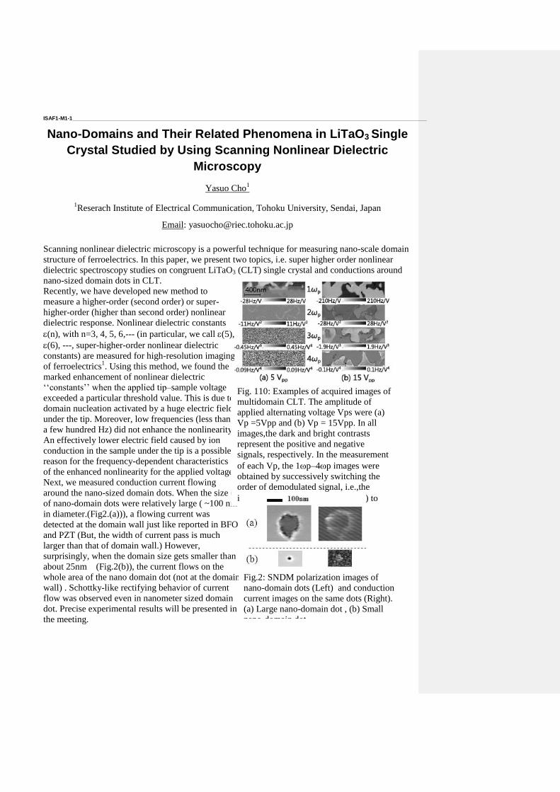
ISAF1-M1-1 _____________________________________________________________________________________________________________________
Nano-Domains and Their Related Phenomena in LiTaO3 Single
Crystal Studied by Using Scanning Nonlinear Dielectric
Microscopy
Yasuo Cho1
1Reserach Institute of Electrical Communication, Tohoku University, Sendai, Japan
Email: [email protected]
Scanning nonlinear dielectric microscopy is a powerful technique for measuring nano-scale domain
structure of ferroelectrics. In this paper, we present two topics, i.e. super higher order nonlinear
dielectric spectroscopy studies on congruent LiTaO3 (CLT) single crystal and conductions around
nano-sized domain dots in CLT.
Recently, we have developed new method to
measure a higher-order (second order) or super-
higher-order (higher than second order) nonlinear
dielectric response. Nonlinear dielectric constants
(n), with n=3, 4, 5, 6,--- (in particular, we call (5),
(6), ---, super-higher-order nonlinear dielectric
constants) are measured for high-resolution imaging
of ferroelectrics1. Using this method, we found the
marked enhancement of nonlinear dielectric
‘‘constants’’ when the applied tip–sample voltage
exceeded a particular threshold value. This is due to
domain nucleation activated by a huge electric field
under the tip. Moreover, low frequencies (less than
a few hundred Hz) did not enhance the nonlinearity.
An effectively lower electric field caused by ion
conduction in the sample under the tip is a possible
reason for the frequency-dependent characteristics
of the enhanced nonlinearity for the applied voltage.
Next, we measured conduction current flowing
around the nano-sized domain dots. When the size of
of nano-domain dots were relatively large ( ~100 nm
in diameter.(Fig2.(a))), a flowing current was
detected at the domain wall just like reported in BFO
and PZT (But, the width of current pass is much
larger than that of domain wall.) However,
surprisingly, when the domain size gets smaller than
about 25nm (Fig.2(b)), the current flows on the
whole area of the nano domain dot (not at the domain
wall) . Schottky-like rectifying behavior of current
flow was observed even in nanometer sized domain
dot. Precise experimental results will be presented in
the meeting.
Fig. 110: Examples of acquired images of
multidomain CLT. The amplitude of
applied alternating voltage Vps were (a)
Vp =5Vpp and (b) Vp = 15Vpp. In all
images,the dark and bright contrasts
represent the positive and negative
signals, respectively. In the measurement
of each Vp, the 1p–4p images were
obtained by successively switching the
order of demodulated signal, i.e.,the
images from 1p to 4p (from (3) to
(6) signal, respectively.) were taken in
from the 1st to 4th quarters of a scanned
area.
Fig.2: SNDM polarization images of
nano-domain dots (Left) and conduction
current images on the same dots (Right).
(a) Large nano-domain dot , (b) Small
nano-domain dot.

1 N. Chinone et al. “Lateral resolution improvement in scanning nonlinear dielectric microscopy by measuring super-
higher-order nonlinear dielectric constants”, Appl. Phys.Lett., vol. 101,213112, 2012.
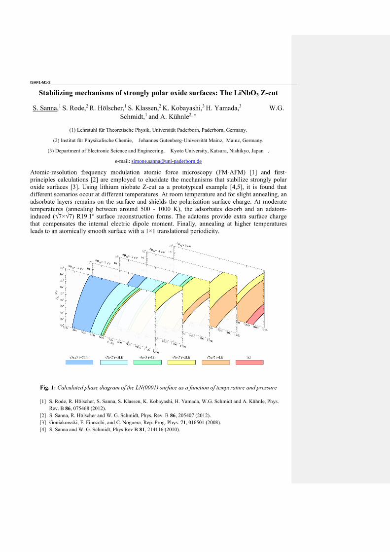
ISAF1-M1-2 _____________________________________________________________________________________________________________________
Stabilizing mechanisms of strongly polar oxide surfaces: The LiNbO3 Z-cut
S. Sanna,1 S. Rode,2 R. Hölscher,1 S. Klassen,2 K. Kobayashi,3 H. Yamada,3 W.G.
Schmidt,1 and A. Kühnle2, ∗
(1) Lehrstuhl für Theoretische Physik, Universität Paderborn, Paderborn, Germany.
(2) Institut für Physikalische Chemie, Johannes Gutenberg-Universität Mainz, Mainz, Germany.
(3) Department of Electronic Science and Engineering, Kyoto University, Katsura, Nishikyo, Japan .
e-mail: [email protected]
Atomic-resolution frequency modulation atomic force microscopy (FM-AFM) [1] and first-
principles calculations [2] are employed to elucidate the mechanisms that stabilize strongly polar
oxide surfaces [3]. Using lithium niobate Z-cut as a prototypical example [4,5], it is found that
different scenarios occur at different temperatures. At room temperature and for slight annealing, an
adsorbate layers remains on the surface and shields the polarization surface charge. At moderate
temperatures (annealing between around 500 - 1000 K), the adsorbates desorb and an adatom-
induced (√7×√7) R19.1° surface reconstruction forms. The adatoms provide extra surface charge
that compensates the internal electric dipole moment. Finally, annealing at higher temperatures
leads to an atomically smooth surface with a 1×1 translational periodicity.
Fig. 1: Calculated phase diagram of the LN(0001) surface as a function of temperature and pressure
[1] S. Rode, R. Hölscher, S. Sanna, S. Klassen, K. Kobayashi, H. Yamada, W.G. Schmidt and A. Kühnle, Phys.
Rev. B 86, 075468 (2012).
[2] S. Sanna, R. Hölscher and W. G. Schmidt, Phys. Rev. B 86, 205407 (2012).
[3] Goniakowski, F. Finocchi, and C. Noguera, Rep. Prog. Phys. 71, 016501 (2008).
[4] S. Sanna and W. G. Schmidt, Phys Rev B 81, 214116 (2010).

[5] S. V. Levchenko and A. M. Rappe, Phys. Rev. Lett. 100 (2008).
ISAF1-M1-3 _____________________________________________________________________________________________________________________
Strain and chemical engineering in LiNbO3 and LiTaO3 thin
films
A.Bartasyte1, V. Plausinaitiene
2, A. Abrutis
2, S. Margueron
3, T. Murauskas
2, P. Boulet
1, V.
Kubilius2, Z. Saltyte
2
1Institute Jean Lamour, (UMR 7198) CNRS – Lorraine University, Nancy, France
2University of Vilnius, Dept. of General and Inorganic Chemistry, Vilnius, Lithuania
3Laboratoire Matériaux Optiques, Photonique et Systèmes, EA 4423, Lorraine University and
Supelec, Metz, France
Email: [email protected]
LiNbO3 and LiTaO3 are the two of the most important crystals, being the equivalent in the field of
optics, nonlinear optics and optoelectronics to silicon in electronics. Optically isotropic ferroelectric
materials (for thermal sensing) or piezoelectric materials with reduced temperature coefficient of
frequency (for acoustic delays lines/resonators) were obtained by chemical engineering of LiNbO3
and LiTaO3348,349
. Thus, the studies about epitaxial ferroelectric LiNbO3 and LiTaO3 thin films are
of great interest because of their potential application as miniaturized and integrated elements in
static random access memories, high dielectric constant capacitors, acoustic delay lines, resonators,
pyroelectric sensors, and optical waveguides. Although LiNbO3 and LiTaO3 films have been
fabricated by different techniques, many electrical and electro-optical properties reported are not
comparable for those of LiNbO3 and LiTaO3 single-crystals. The growth of high quality
LiNbO3/LiTaO3 films is far from being a routine due to a difficulty to estimate the phase
composition and Li stoichiometry. Thus, the deposited films are hardly reproducible, often contain
undesirable phases (for example, LiNb3O8 or Li3NbO4) or are stoichiometrically inhomogeneous.
This inhibits the applications of the materials in the thin film form.
In this work, the physical and structural properties of LiTaO3 and LiNbO3 thin films were tuned by
changing their chemical composition and strain state. The possibility to change by several times the
thermal expansion of LiNbO3/LiTaO3 thin films by applying biaxial strain was observed. This
opens new avenues for temperature compensated devices350
. Moreover, the indirect methods, used
to estimate Li concentration in the single crystals, cannot be applied directly due to the presence of
strain, size effects or other defects in the films, which influences also the structural, optical and
other physical properties. Thus, the indirect method for estimation of nonstoichiometry of LiNbO3
and LiTaO3 films, based on Curie temperature and dampings of Raman modes and taking into
account secondary effects, was developed.
348
A.M. Glazer, P.A. Thomas, N. Zhang, A. Bartasyte, D.S. Keeble, Patent WO/2011/158022, 2011.
349 A. Bartasyte and O. Elmazria, Patent F12 52410, 2012.
350 A. Bartasyte, V. Plausinaitiene, A. Abrutis, T. Murauskas, P. Boulet, S. Margueron, J. Gleize, S. Robert, V.
Kubilius, and Z. Saltyte, Appl. Phys. Lett., 101, 122902, 2012.
ISAF1-M1-4 _____________________________________________________________________________________________________________________
Study of LiNb1-xTaxO3 mixed crystals by Raman and IR
spectroscopy
A.Bartasyte1,2
, S. Margueron3, A.M. Glazer
2, E. Simon
4, J. Hlinka
4, I. Gregora
4, P.A. Thomas
5
1Institute Jean Lamour, (UMR 7198) CNRS – Lorraine University, Nancy, France 2Department of Physics, Oxford University, Parks Road, Oxford OX1 3PU, UK
3Laboratoire Matériaux Optiques, Photonique et Systèmes, EA 4423, Lorraine University and
Supelec, Metz, France 4Institute of Physics AS CR, Prague 8, Czech Republic
5Department of Physics, University of Warwick, Coventry, UK
Email: [email protected]
Lithium niobate (LN) and lithium tantalate (LT) have been subject of intense studies because of
their optical applications in industry. At room temperature LN and LT are isomorphous and
ferroelectric, crystallizing in the space group R3c. The ferroelectric LN and LT crystal structure can
be described in terms of polar displacements of the cations along the [0001] direction, with corner-
linked oxygen octahedra tilted according to the system a-a
-a
-. Despite LT and LN structural
similarity, these materials have different physical properties. Therefore, LiNb1-xTaxO3 (LNTx)
materials are of special interest because their properties can be tuned between those of LN and
LT351
. However, the fundamental properties of LNTx solid solutions have not yet been investigated
sufficiently to date.
The dynamical properties of LN and LT have been intensively studied. The optical phonon
frequencies, damping parameters, and intensities are of special interest in studies of phase
transitions, symmetry, effect of pressure, stress, composition and heterogeneities in thin films,
integrated structures, nano and bulk materials. It is essential to know the frequencies in calculations
of dielectric constant , oblique modes , and electro-optic coefficients. There are numerous reports
concerning optical phonons in LT and LN, studied by Raman and infrared spectroscopies352
,
neutron inelastic scattering and theoretically. Generaly speaking, dynamical properties of different
type of solid solutions have been extensively studied in literature. Nevertheless, there is only one
report on the study of LNT solid-solution zone-centre phonons.353
The authors studied only
LNT0.9, and claimed that the Raman mode assignment is similar to that of LT. LNTx with other
compositions of solid solutions and the change of zone-centre phonons with Ta/Nb ratio have never
been studied.
In this work, all 26 optical phonons at Γ point of LNTx single crystals were identified in polarized
spectra measured by IR and Raman spectroscopies. The effect of Nb replacement by Ta on the
351
A. Bartasyte, A.M. Glazer, F. Wondre, D. Prabhakaran, P.A. Thomas, S. Huband, D.S. Keeble, and S. Margueron,
Mater. Chem. Phys. 134, 728-735, 2012. 352
S. Margueron, A. Bartasyte, A.M. Glazer, E. Simon, J. Hlinka, I. Gregora, and J. Gleize, J. Appl. Phys. 111, 104105,
2012.
353 Ge, Y.-C. and C.-Z. Zhao. J. Raman Spectroscopy, 26, 975-979, 1995.

wavenumbers, Raman efficiency coefficients, oblique mode dispersion and overlap matrix of zone-
centre phonons over the whole composition range 0 ≤ x ≤ 1 was described.
ISAF1-M1-5 _____________________________________________________________________________________________________________________
Charged Domain Wall Conductivity in Lithium Niobate
and Lithium Tantalate Single Crystals
Baturin Ivan1,2
, Chezganov Dmitry1, Esin Alexander
1, Shur Vladimir
1,2,
Akhmatkhanov Andrey1,2
, Ksenofontov Danila1
1Ferroelectric Laboratory, Ural Federal University, Ekaterinburg, Russia
2Labfer Ltd., Ekaterinburg, Russia
Email: [email protected]
Charged domain wall conductivity in lithium niobate (LN) and lithium tantalate (LT) single crystals
and its relaxation after polarization reversal have been studied. Strong increase of the conductivity
along the charged domain walls (CDW) was shown for the first time for head-to-head domain
structure in ferroelectric semiconductor SbSIxxxi
. Recently conduction properties of domain walls
have attract a great attention with the progress in AFM characterization techniques. Electronic
conductivity along ferroelectric domain walls in multiferroic BiFeO3xxxii
was observed using c-
AFM measurements. Moreover, the reversible resistance transition caused by the polarization
reversalxxxiii
was found in ferroelectric MgO doped LN crystals, which is extensively used for
domain-engineered QPM nonlinear optical applications. Recently, the domain wall conductivity in
LN was studied by c-AFM in the presence of UV illuminationxxxiv
. The observed resistive change
behavior is believed to be useful for memory applications2,3
.
Z-cut LN and LT crystals with congruent and near stoichiometric composition as well as with MgO
doping have been used for the present study. CDW were fabricated by polarization reversal by
application of the electric field at elevated temperature (100-250oC) using metal electrodes
deposited on both sides of z-cut samplesxxxv
. Strong increase of the conductivity current was
observed during polarization reversal in all studied LN and LT crystals due to CDW formation. This
strongly affects the domain patterning in MgO doped LN leading to decrease of applied field and
sample fracture due to local heating. Absence of significant conductivity during polarization
reversal using liquid electrodes was attributed to formation of the neutral walls only.
Partial switching with different fraction of the switched area followed by immediate current
measurement was used to study the domain wall conductivity in details. It was shown that the
domain wall conductivity essentially relaxes after partial polarization reversal following exponential
decay behavior with the characteristics time of about tens of seconds. It was found that maximum
value of conductivity current is proportional to the switched area, which determines the total length
of CDW. The maximum value of the effective conductivity was found to be several orders of
magnitude higher than for single domain sample.
The equipment of the UCSU “Modern Nanotechnology”, Institute of Natural Sciences, UrFU has
been used. The research was made possible in part by RFBR (Grants 13-02-01391-а, 11-02-91066-
CNRS-а), by Ministry of Education and Science (Сontract 14.513.12.0006) and with the financial
support of young scientists in terms of Ural Federal University development program.

Piezoelectrics
CLUB B
Thursday, July 25 2013, 02:00 pm - 03:30 pm
Chair: To Be Aannounced
ISAF2-M2-1 _____________________________________________________________________________________________________________________
Dielectric & Piezoelectric Enhancement of Potassium
Niobate/Barium Titanate Nano-complex Ceramics with Parallel
Configuration of Structure-gradient Regions
Satoshi Wada1, Hideto Kawashima
1, Shintarou Ueno
1, Kouichi Nakashima
1, and
Nobuhiro Kumada1
1Material Science and Technology, Interdisciplinary Graduate School of Medical and Engineering,
University of Yamanashi, 4-4-37 takeda, Kofu, Yamanashi 400-8510, Japan
Email: [email protected]
Barium titanate (BaTiO3, BT) and potassium niobate (KNbO3, KN) (BT-KN) nano-structured
ceramics with artificial morphotropic phase boundary (MPB) structure were successfully prepared
by solvothermal method at temperatures below 230 ˚C. Especially, structure-gradient region (SGR)
can be expected to enhance piezoelectric and dielectric properties, and then, to induce parallel
configuration of SGR, new preparation method was proposed and developed in this study. As the
results, KN epitaxial layer was successfully deposited on BT nanoparticle accumulation with
necking structure between neighbored BT nanoparticles. Various characterizations confirmed that
the BT-KN nano-structured ceramics exhibited BT/KN molar ratio of 1, a porosity of around 30 %
and heteroepitaxial interface between BT and KN. Their apparent piezoelectric constant d33* was
estimated at 300 pC/N, and was eight times larger value than that of the 0.5BT-0.5KN dense
ceramics, while dielectric constant was estimated at 1600 at room temperature. The concept
proposed in this study can be a new way to create piezoelectric ceramics with artificial MPB region.
Moreover, this method is very universal and applied into various functional materials such as
magnetic, conductive, semi-conductive, and optical materials in addition to dielectric, piezoelectric
and ferroelectric materials. In the future, we will develop various new materials with
heteroepitaxial interfaces on the basis of the concept.
ISAF2-M2-2 _____________________________________________________________________________________________________________________
Chemically Modified Solution-Derived Na0.5K0.5NbO3 Thin
Films: From Macro- to Nanoscale Response
Sebastjan Glinšek1, Seung-Hyun Kim
1, Lindsay Kuhn
1, Alice Leung
1 and Angus Kingon
1
1School of Engineering, Brown University, Providence, USA
Email: [email protected]
A great potential for applications in micro- and nanoscale devices is a driving force for the still-
growing interest in thin-film piezoelectric materials. Among huge amount of applications, micro-
electro-mechanical system (MEMS) piezoelectric vibration energy harvesters could be used for
powering medical implants.354
For this purpose both thin-film and substrate materials have to be
non-toxic. For the substrates, stainless steel foils are good candidates since they are bio-compatible,
flexible and enable high-temperature processing, as well as ease of microfabrication.
The (Na,K)NbO3-based materials (NKN) are among the most promising lead-free piezoelectrics.355
However, in the thin-film form their properties are regularly deteriorated compared to the bulk
counterparts. It is believed that the problem arises mainly from high and differential volatility of
alkali compounds during heating. Therefore their functional properties are still not well understood,
in particular, there is a strong need to link the measured macroscopic properties to the nanoscale
domain structure and local switching behavior.
With the aim of improving functional response NKN is often chemically modified. Our group
recently reported on strong enhancement of functional properties of the solution-derived NKN-
based thin films by the addition of small amounts of BiFeO3 (BFO). The films with 5 % BFO have
room-temperature value of the kHz-dielectric permittivity~600, leakage current density ~10-7
A/cm2 and piezoelectric coefficient d33 ~57 pm/V.
356
In this paper our recent advances on NKN, NKN-LN (LiNbO3) and NKN-BFO solution-derived
films will be presented. The phase-pure perovskite films were prepared either on standard platinized
silicon or flexible stainless steel substrates. In addition to the macroscale functional
characterization, piezoresponse force microscopy was employed to study domain structure and local
polarization switching behavior. Influence of different dopants, substrates and relationships between
the macroscopic performance and nanoscale properties will be addressed.
354
S.-G. Kim, S. Priya, I. Kanno, “Piezoelectric MEMS for Energy Harvesting”, MRS Bullettin, vol. 37, p. 1039 -50,
2012 355
J. Rodel, W. Jo, T. P. Seifert et al., “Perspective on the Development of Lead-Free Piezoceramics”, J. Am. Ceram.
Soc., vol. 92, p. 1153-77, 2009 356
S.-H. Kim, A. Leung, C. Y. Koo et al., “Lead-Free (Na0.5K0.5)(Nb0.95Ta0.05)O3-BiFeO3 Thin Films for MEMS
Piezoelectric Vibration Energy Harvesting Devices”, Mater. Lett., vol. 69, p. 24-26, 2012
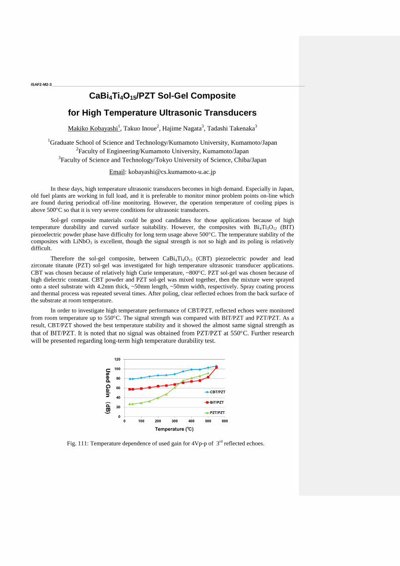
ISAF2-M2-3 _____________________________________________________________________________________________________________________
CaBi4Ti4O15/PZT Sol-Gel Composite
for High Temperature Ultrasonic Transducers
Makiko Kobayashi1, Takuo Inoue
2, Hajime Nagata
3, Tadashi Takenaka
3
1Graduate School of Science and Technology/Kumamoto University, Kumamoto/Japan
2Faculty of Engineering/Kumamoto University, Kumamoto/Japan
3Faculty of Science and Technology/Tokyo University of Science, Chiba/Japan
Email: [email protected]
In these days, high temperature ultrasonic transducers becomes in high demand. Especially in Japan,
old fuel plants are working in full load, and it is preferable to monitor minor problem points on-line which
are found during periodical off-line monitoring. However, the operation temperature of cooling pipes is
above 500C so that it is very severe conditions for ultrasonic transducers.
Sol-gel composite materials could be good candidates for those applications because of high
temperature durability and curved surface suitability. However, the composites with Bi4Ti3O12 (BIT)
piezoelectric powder phase have difficulty for long term usage above 500C. The temperature stability of the
composites with LiNbO3 is excellent, though the signal strength is not so high and its poling is relatively
difficult.
Therefore the sol-gel composite, between CaBi4Ti4O15 (CBT) piezoelectric powder and lead
zirconate titanate (PZT) sol-gel was investigated for high temperature ultrasonic transducer applications.
CBT was chosen because of relatively high Curie temperature, ~800C. PZT sol-gel was chosen because of
high dielectric constant. CBT powder and PZT sol-gel was mixed together, then the mixture were sprayed
onto a steel substrate with 4.2mm thick, ~50mm length, ~50mm width, respectively. Spray coating process
and thermal process was repeated several times. After poling, clear reflected echoes from the back surface of
the substrate at room temperature.
In order to investigate high temperature performance of CBT/PZT, reflected echoes were monitored
from room temperature up to 550C. The signal strength was compared with BIT/PZT and PZT/PZT. As a
result, CBT/PZT showed the best temperature stability and it showed the almost same signal strength as
that of BIT/PZT. It is noted that no signal was obtained from PZT/PZT at 550C. Further research
will be presented regarding long-term high temperature durability test.
Fig. 111: Temperature dependence of used gain for 4Vp-p of 3rd
reflected echoes.
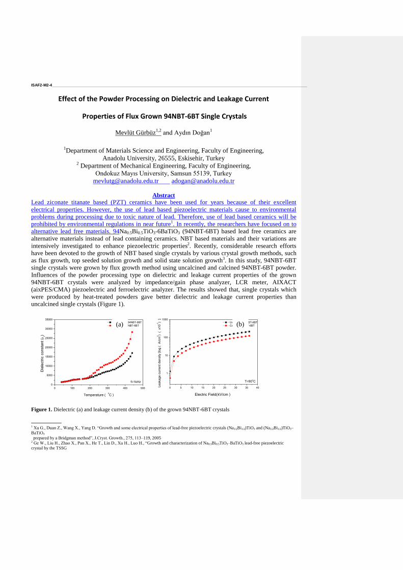
ISAF2-M2-4 _____________________________________________________________________________________________________________________
Effect of the Powder Processing on Dielectric and Leakage Current
Properties of Flux Grown 94NBT-6BT Single Crystals
Mevlüt Gürbüz1,2
and Aydın Doğan1
1Department of Materials Science and Engineering, Faculty of Engineering,
Anadolu University, 26555, Eskisehir, Turkey 2 Department of Mechanical Engineering, Faculty of Engineering,
Ondokuz Mayıs University, Samsun 55139, Turkey
[email protected] [email protected]
Abstract
Lead ziconate titanate based (PZT) ceramics have been used for years because of their excellent
electrical properties. However, the use of lead based piezoelectric materials cause to environmental
problems during processing due to toxic nature of lead. Therefore, use of lead based ceramics will be
prohibited by environmental regulations in near future1. In recently, the researchers have focused on to
alternative lead free materials. 94Na0.5Bi0.5TiO3-6BaTiO3 (94NBT-6BT) based lead free ceramics are
alternative materials instead of lead containing ceramics. NBT based materials and their variations are
intensively investigated to enhance piezoelectric properties2. Recently, considerable research efforts
have been devoted to the growth of NBT based single crystals by various crystal growth methods, such
as flux growth, top seeded solution growth and solid state solution growth3. In this study, 94NBT-6BT
single crystals were grown by flux growth method using uncalcined and calcined 94NBT-6BT powder.
Influences of the powder processing type on dielectric and leakage current properties of the grown
94NBT-6BT crystals were analyzed by impedance/gain phase analyzer, LCR meter, AIXACT
(aixPES/CMA) piezoelectric and ferroelectric analyzer. The results showed that, single crystals which
were produced by heat-treated powders gave better dielectric and leakage current properties than
uncalcined single crystals (Figure 1).
Figure 1. Dielectric (a) and leakage current density (b) of the grown 94NBT-6BT crystals
1 Xu G., Duan Z., Wang X., Yang D. “Growth and some electrical properties of lead-free piezoelectric crystals (Na1/2Bi1/2)TiO3 and (Na1/2Bi1/2)TiO3–BaTiO3
prepared by a Bridgman method”, J.Cryst. Growth., 275, 113–119, 2005 2 Ge W., Liu H., Zhao X., Pan X., He T., Lin D., Xu H., Luo H., “Growth and characterization of Na0.5Bi0.5TiO3–BaTiO3 lead-free piezoelectric crystal by the TSSG
0 5 10 15 20 25 30 35 40
1
10
100
1000
Leakage c
urr
ent density [lo
g (
A/c
m2)
(x10
-7)
]
Electric Field(kV/cm )
Uncalcined 94NBT-6BT
Calcined 94NBT-6BT
T=90oC
0 100 200 300 400 500
0
5000
10000
15000
20000
25000
30000
35000
Temperature (oC )
Die
lectr
ic c
on
sta
nt
(r)
Uncalcined 94NBT-6BT
Calcined 94NBT-6BT
f=1kHz
(a) (b)

method”, J. Alloy. Compd., 456, 503–507, 2008 3Moon K.S., Rout D., Lee H.Yong., Kang S.J. L., “Solid state growth of Na1/2Bi1/2TiO3–BaTiO3 single crystals and their enhanced piezoelectric
properties”, J. Cryst.
Growth., 317, 28-31, 2011
ISAF2-M2-5 _____________________________________________________________________________________________________________________
Growth, Properties and Structure of High Performance PIN-PMN-PT Single Crystals
Zhuo Xu, Zhenrong Li, Fei Li, Shiji Fan and Xi Yao Electronic Materials Research Laboratory, Key Laboratory of the Ministry of Education & International Center
for Dielectric Research, Xi’an Jiaotong University, Xi’an 710049, China
Ternary Pb(In1/2Nb1/2)O3-Pb(Mg1/3Nb2/3)O3-PbTiO3 (PIN-PMN-PT) crystals with
morphotropic phase boundary (MPB) composition have attracted much interest due to the higher
ferroelectric-ferroelectric transition temperature TR-T (>120oC), improved EC (~5kV/cm), and
similar piezoelectric properties (d33>1500 pC/N, k33>90%), when compared to binary
Pb(Mg1/3Nb2/3)O3-PbTiO3 (PMN-PT) crystals. These properties make PIN-PMN-PT crystals good
candidates for various transducer applications.
The paper reviews the recent progress of research on growth, piezoelectric/dielectric properties
and structure of PIN-PMN-PT single crystal in Xi’an Jiaotong University. (1) PIN-PMN-PT single
crystals of 2’ diameter and 3’ diameter were grown by the modified Bridgman technique. Variations
of composition of PIN-PMN-PT single crystal along growth direction were presented. The
homogeneity of PIN-PMN-PT single crystals is needed to be improved in the future. (2) Variations
of piezoelectric/dielectric properties of PIN-PMN-PT single crystal along growth direction were
measured in detailed. Phase transition characteristics of PIN-PMN-PT single crystals with different
composition were investigated. The phase diagram of PIN-PMN-PT was built. (3) The high shear
piezoelectric response with improved thermal stability (d24~2000 pC/N) was obtained in
orthorhombic crystals. Meanwhile, the high electromechanical couplings k33 (>84%) and
mechanical quality factors Q (>2000) were concurrently obtained in tetragonal crystals with
broadened temperature usage range. (4) Domain size effect in PIN-PMN-PT single crystal was
studied. The piezoelectric constant d33 is improved with decreasing domain size. The fitting curve
of the relationship between the domain size and d33 was obtained.
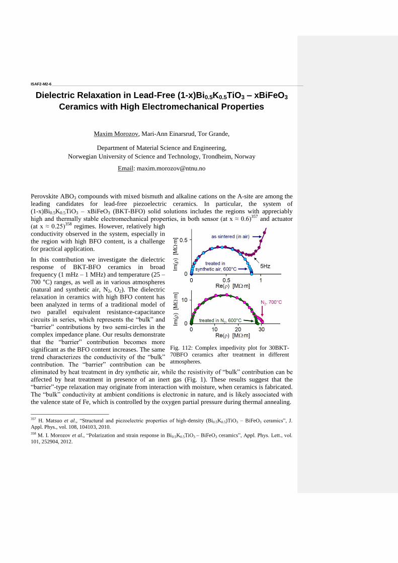
ISAF2-M2-6 _____________________________________________________________________________________________________________________
Dielectric Relaxation in Lead-Free (1-x)Bi0.5K0.5TiO3 – xBiFeO3
Ceramics with High Electromechanical Properties
Maxim Morozov, Mari-Ann Einarsrud, Tor Grande,
Department of Material Science and Engineering,
Norwegian University of Science and Technology, Trondheim, Norway
Email: [email protected]
Perovskite ABO3 compounds with mixed bismuth and alkaline cations on the A-site are among the
leading candidates for lead-free piezoelectric ceramics. In particular, the system of
(1-x)Bi0.5K0.5TiO3 – xBiFeO3 (BKT-BFO) solid solutions includes the regions with appreciably
high and thermally stable electromechanical properties, in both sensor (at x ≈ 0.6)357
and actuator
(at x ≈ 0.25)358
regimes. However, relatively high
conductivity observed in the system, especially in
the region with high BFO content, is a challenge
for practical application.
In this contribution we investigate the dielectric
response of BKT-BFO ceramics in broad
frequency (1 mHz – 1 MHz) and temperature (25 –
700 °C) ranges, as well as in various atmospheres
(natural and synthetic air, N2, O2). The dielectric
relaxation in ceramics with high BFO content has
been analyzed in terms of a traditional model of
two parallel equivalent resistance-capacitance
circuits in series, which represents the “bulk” and
“barrier” contributions by two semi-circles in the
complex impedance plane. Our results demonstrate
that the “barrier” contribution becomes more
significant as the BFO content increases. The same
trend characterizes the conductivity of the “bulk”
contribution. The “barrier” contribution can be
eliminated by heat treatment in dry synthetic air, while the resistivity of “bulk” contribution can be
affected by heat treatment in presence of an inert gas (Fig. 1). These results suggest that the
“barrier”-type relaxation may originate from interaction with moisture, when ceramics is fabricated.
The “bulk” conductivity at ambient conditions is electronic in nature, and is likely associated with
the valence state of Fe, which is controlled by the oxygen partial pressure during thermal annealing.
357
H. Matsuo et al., “Structural and piezoelectric properties of high-density (Bi0.5K0.5)TiO3 – BiFeO3 ceramics”, J.
Appl. Phys., vol. 108, 104103, 2010. 358
M. I. Morozov et al., “Polarization and strain response in Bi0.5K0.5TiO3 – BiFeO3 ceramics”, Appl. Phys. Lett., vol.
101, 252904, 2012.
Fig. 112: Complex impedivity plot for 30BKT-
70BFO ceramics after treatment in different
atmospheres.

Thus, our study demonstrates the way to improve electric resistivity in BKT-BFO ceramics.

Smart Materials and Devices
CLUB C
Thursday, July 25 2013, 02:00 pm - 03:30 pm
Chair: To Be Announced
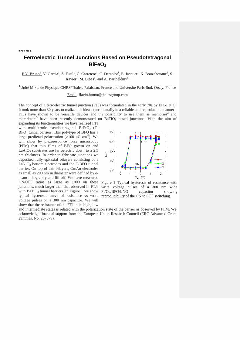
ISAF4-M3-1 _____________________________________________________________________________________________________________________
Ferroelectric Tunnel Junctions Based on Pseudotetragonal
BiFeO3
F.Y. Bruno1, V. Garcia
1, S. Fusil
1, C. Carretero
1, C. Deranlot
1, E. Jacquet
1, K. Bouzehouane
1, S.
Xavier1, M. Bibes
1, and A. Barthélémy
1.
1Unité Mixte de Physique CNRS/Thales, Palaiseau, France and Université Paris-Sud, Orsay, France
Email: [email protected]
The concept of a ferroelectric tunnel junction (FTJ) was formulated in the early 70s by Esaki et al.
It took more than 30 years to realize this idea experimentally in a reliable and reproducible manner1.
FTJs have shown to be versatile devices and the possibility to use them as memories2 and
memristors3 have been recently demonstrated on BaTiO3 based junctions. With the aim of
expanding its functionalities we have realized FTJ
with multiferroic pseudotetragonal BiFeO3 (T-
BFO) tunnel barriers. This polytype of BFO has a
large predicted polarization (>100 μC cm-2
). We
will show by piezoresponce force microscopy
(PFM) that thin films of BFO grown on and
LaAlO3 substrates are ferroelectric down to a 2.5
nm thickness. In order to fabricate junctions we
deposited fully epitaxial bilayers consisting of a
LaNiO3 bottom electrodes and the T-BFO tunnel
barrier. On top of this bilayers, Co/Au electrodes
as small as 200 nm in diameter were defined by e-
beam lithography and lift-off. We have measured
ON/OFF ratios as large as 1000 on these
junctions, much larger than that observed in FTJs
with BaTiO3 tunnel barriers. In Figure 1 we show
typical hysteresis curve of resistance vs write
voltage pulses on a 300 nm capacitor. We will
show that the resistance of the FTJ in its high, low
and intermediate states is related with the polarization state of the barrier as observed by PFM. We
acknowledge financial support from the European Union Research Council (ERC Advanced Grant
Femmes, No. 267579).
Figure 1 Typical hysteresis of resistance with
write voltage pulses of a 300 nm wide
Pt/Co/BFO/LNO capacitor showing
reproducibility of the ON to OFF switching.
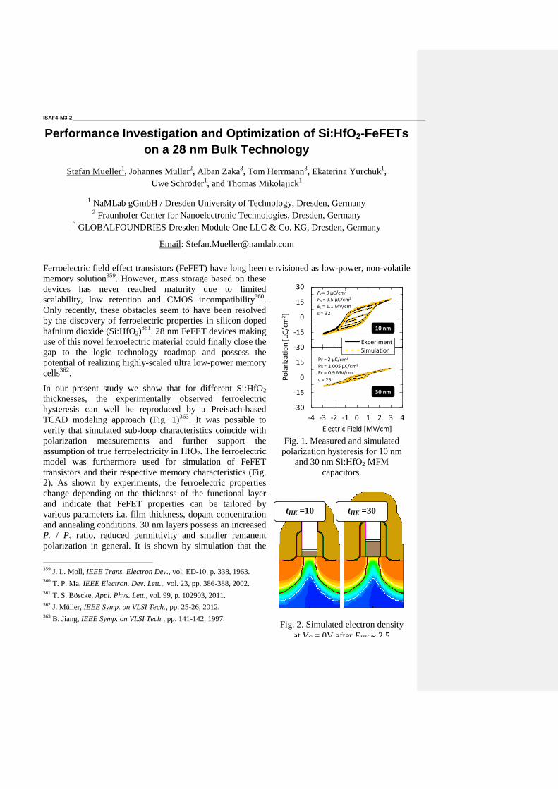
ISAF4-M3-2 _____________________________________________________________________________________________________________________
Performance Investigation and Optimization of Si:HfO2-FeFETs
on a 28 nm Bulk Technology
Stefan Mueller1, Johannes Müller
2, Alban Zaka
3, Tom Herrmann
3, Ekaterina Yurchuk
1,
Uwe Schröder1, and Thomas Mikolajick
1
1 NaMLab gGmbH / Dresden University of Technology, Dresden, Germany 2 Fraunhofer Center for Nanoelectronic Technologies, Dresden, Germany
3 GLOBALFOUNDRIES Dresden Module One LLC & Co. KG, Dresden, Germany
Email: [email protected]
Ferroelectric field effect transistors (FeFET) have long been envisioned as low-power, non-volatile
memory solution359
. However, mass storage based on these
devices has never reached maturity due to limited
scalability, low retention and CMOS incompatibility360
.
Only recently, these obstacles seem to have been resolved
by the discovery of ferroelectric properties in silicon doped
hafnium dioxide (Si:HfO2)361
. 28 nm FeFET devices making
use of this novel ferroelectric material could finally close the
gap to the logic technology roadmap and possess the
potential of realizing highly-scaled ultra low-power memory
cells362
.
In our present study we show that for different Si:HfO2
thicknesses, the experimentally observed ferroelectric
hysteresis can well be reproduced by a Preisach-based
TCAD modeling approach (Fig. 1)363
. It was possible to
verify that simulated sub-loop characteristics coincide with
polarization measurements and further support the
assumption of true ferroelectricity in HfO2. The ferroelectric
model was furthermore used for simulation of FeFET
transistors and their respective memory characteristics (Fig.
2). As shown by experiments, the ferroelectric properties
change depending on the thickness of the functional layer
and indicate that FeFET properties can be tailored by
various parameters i.a. film thickness, dopant concentration
and annealing conditions. 30 nm layers possess an increased
Pr / Ps ratio, reduced permittivity and smaller remanent
polarization in general. It is shown by simulation that the
359
J. L. Moll, IEEE Trans. Electron Dev., vol. ED-10, p. 338, 1963. 360
T. P. Ma, IEEE Electron. Dev. Lett.,, vol. 23, pp. 386-388, 2002. 361
T. S. Böscke, Appl. Phys. Lett., vol. 99, p. 102903, 2011. 362
J. Müller, IEEE Symp. on VLSI Tech., pp. 25-26, 2012. 363
B. Jiang, IEEE Symp. on VLSI Tech., pp. 141-142, 1997.
Fig. 1. Measured and simulated
polarization hysteresis for 10 nm
and 30 nm Si:HfO2 MFM
capacitors.
Fig. 2. Simulated electron density
at VG = 0V after EHK 2.5
MV/cm program operation.
-30
-15
0
15
30
-4 -3 -2 -1 0 1 2 3 4
Po
lari
zati
on
[µC
/cm
2]
Electric Field [MV/cm]
Pr = 2 µC/cm2
Ps = 2.005 µC/cm2
Ec = 0.9 MV/cm
= 25
-30
-15
0
15
30P
ola
riza
tio
n [µ
C/c
m2]
Experiment
Simulation
Pr = 9 µC/cm2
Ps = 9.5 µC/cm2
Ec = 1.1 MV/cm
= 32
-30
-15
0
15
30
-4 -3 -2 -1 0 1 2 3 4
Po
lari
zati
on
[µC
/cm
2]
Electric Field [MV/cm]
Pr = 2 µC/cm2
Ps = 2.005 µC/cm2
Ec = 0.9 MV/cm
= 25
10 nm
30 nm
tHK =10
nm
tHK =30
nm

interfacial field stress can be reduced using thicker Si:HfO2 layers which might contribute to FeFET
endurance optimization in the future.
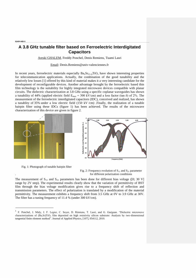
ISAF4-M3-3 _____________________________________________________________________________________________________________________
A 3.8 GHz tunable filter based on Ferroelectric Interdigitated Capacitors
Areski GHALEM, Freddy Ponchel, Denis Remiens, Tuami Lasri
Email: [email protected]
In recent years, ferroelectric materials especially BaxSr(1-x)TiOx have shown interesting properties
for telecommunication applications. Actually, the combination of the good tunability and the
relatively low losses [1] offered by this kind of material makes it a very interesting candidate for the
development of reconfigurable devices. Another advantage brought by the ferroelectric based thin
film technology is the suitability for highly integrated microwave devices compatible with planar
circuits. The dielectric characterization at 3.8 GHz using a specific coplanar waveguides has shown
a tunability of 44% (applied electric field Emax = 300 kV/cm) and a loss factor (tan δ) of 2%. The
measurement of the ferroelectric interdigitated capacitors (IDC), conceived and realized, has shown
a tunablity of 35% under a low electric field (150 kV /cm) .Finally, the realization of a tunable
hairpin filter using these IDCs (figure 1) has been achieved. The results of the microwave
characterization of this device are given in figure 2.
.
The measurement of S11 and S21 parameters has been done for different bias voltage ([0; 30 V]
range by 2V step). The experimental results clearly show that the variation of permittivity of BST
film through the bias voltage modification gives rise to a frequency shift of reflection and
transmission parameters. The effect of polarization is translated by a modification of the material
permittivity. The measurement exhibits a frequency shift from 3.5 GHz at 0V to 3.9 GHz at 30V.
The filter has a tuning frequency of 11.4 % (under 300 kV/cm).
1 F. Ponchel, J. Midy, J. F. Legier, C. Soyer, D. Rèmiens, T. Lasri, and G. Guéguan. “Dielectric microwave
characterizations of (Ba,Sr)TiO3 film deposited on high resistivity silicon substrate: Analysis by two-dimensional
tangential finite element method”. Journal of Applied Physics, [107], 054112, 2010.
Fig. 1: Photograph of tunable hairpin filter
Fig. 2: Frequency evolution of S11 and S21 parameter
for different polarization conditions
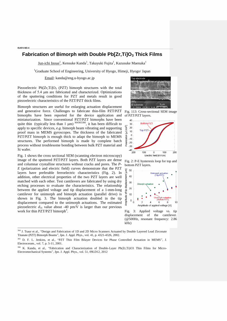
ISAF4-M3-4 _____________________________________________________________________________________________________________________
Fabrication of Bimorph with Double Pb[Zr,Ti]O3 Thick Films
Jun-ichi Inoue1, Kensuke Kanda
1, Takayuki Fujita
1, Kazusuke Maenaka
1
1Graduate School of Engineering, University of Hyogo, Himeji, Hyogo/ Japan
Email: [email protected]
Piezoelectric Pb[Zr,Ti]O3 (PZT) bimorph structures with the total
thickness of 5.4 μm are fabricated and characterized. Optimizations
of the sputtering conditions for PZT and metals result in good
piezoelectric characteristics of the PZT/PZT thick films.
Bimorph structures are useful for enlarging actuation displacement
and generative force. Challenges to fabricate thin-film PZT/PZT
bimorphs have been reported for the device application and
miniaturization. Since conventional PZT/PZT bimorphs have been
quite thin (typically less than 1 μm) 364365366
, it has been difficult to
apply to specific devices, e.g. bimorph beam vibrating and supporting
proof mass in MEMS gyroscopes. The thickness of the fabricated
PZT/PZT bimorph is enough thick to adapt the bimorph to MEMS
structures. The performed bimorph is made by complete batch
process without troublesome bonding between bulk PZT material and
Si wafer.
Fig. 1 shows the cross sectional SEM (scanning electron microscopy)
image of the sputtered PZT/PZT layers. Both PZT layers are dense
and columnar crystalline structures without cracks and pores. The P-
E (polarization and electric field) curves demonstrate that the PZT
layers have preferable ferroelectric characteristics (Fig. 2). In
addition, other electrical properties of the two PZT layers are well
matched with each other. Test cantilevers are fabricated by using dry
etching processes to evaluate the characteristics. The relationship
between the applied voltage and tip displacement of a 1-mm-long
cantilever for unimorph and bimorph actuation (parallel drive) is
shown in Fig. 3. The bimorph actuation doubled in the tip
displacement compared to the unimorph actuations. The estimated
piezoelectric d31 value about -40 pm/V is larger than our previous
work for thin PZT/PZT bimorph3.
364
J. Tsaur et al., “Design and Fabrication of 1D and 2D Micro Scanners Actuated by Double Layered Lead Zirconate
Titanate (PZT) Bimorph Beams”, Jpn. J. Appl. Phys., vol. 41, p. 4321-4326, 2002. 365
D. F. L. Jenkins, et al., “PZT Thin Film Bilayer Devices for Phase Controlled Actuation in MEMS”, J.
Electroceram., vol. 7, p. 5-11, 2001. 366
K. Kanda, et al., “Fabrication and Characterization of Double-Layer Pb(Zr,Ti)O3 Thin Films for Micro-
Electromechanical Systems”, Jpn. J. Appl. Phys., vol. 51, 09LD12, 2012
Top PZT
Bottom PZT
Middle electrode
Bottom electrode
SiO2
Si substrate 3 m
Top electrode
Fig. 113: Cross-sectional SEM image
of PZT/PZT layers.
Fig. 2: P-E hysteresis loop for top and
bottom PZT layers.
Fig. 3: Applied voltage vs. tip
displacement of the cantilever.
(@500Hz, resonant frequency: 2.86
kHz)
ISAF4-M3-5 _____________________________________________________________________________________________________________________
PZT PIEZOELECTRIC FILMS ON GLASS FOR ADJUSTABLE X-RAY OPTICS
Rudeger H.T. Wilke1, Raegan L. Johnson-Wilke
1, Susan Trolier-McKinstry
1, Vincenzo Cotroneo
2,
Stuart McMuldroch2, Paul B. Reid
2 and Daniel A. Schwartz
2
1Materials Research Institute, The Pennsylvania State University, University Park, USA
2Harvard-Smithsonian Center for Astrophysics, Cambridge, USA
Email: [email protected]
Adjustble X-ray optics, using piezoelectric lead zirconate titanate (PZT) films deposited on
slumped, thin glass substrates, are a candidate for the Square Meter Arc Second X-ray Telescope
(SMART-X) mission concept. The mirror pieces are shaped in the form of paraboloids and
hyperboloids with an iridium mirror deposited on the concave surface of the glass and a PZT film
deposited on the convex surface. The geometrical constraints make processing of the PZT films by
chemical solution deposition quite complex. As a result, an RF magnetron sputtering approach has
been adopted. PZT films were deposited on Corning Eagle glass substrates. Two different shaped
substrates were used; one in the form of flat 100 mm rounds and the second in cylinders slumped
along an axial direction with a radius of curvature of 220 mm. Crystallization into the perovskite
phase was performed at 550 oC, approximately 100
oC below the strain point of the glass substrates.
Films deposited on flat round substrates demonstrate the feasibility of using PZT thin films to
provide high precision control of the surface figure of the mirror. Influence function measurements
of the 1.5 μm thick films indicate 2.5 μm out of plane deflection for 1 cm2 actuators at a drive level
of +10 V, in good agreement with finite element analysis models. Depositions onto curved
substrates were carried out using multiple sputter guns to ensure optimal film thickness uniformity
across the two axes of the cylinder. The electrical and eletromechanical properties of the PZT films
on curved glass were comparable to those of films deposited on flat pieces. The permittivity of the
films was 1500 at 100 Hz, with a loss tangent of 0.04. The hysteresis loops were square with
remanent hysteresis values approximately 21 C/cm2 and coercive field values near 30 kV/cm.
Initial results for influence functions on the curved substrates (measured along the axial direction)
show a 0.4 m deflection for an actuator driven at 4 V (40 kV/cm). The deflection profile about the
actuator matches finite element model predictions.

ISAF4-M3-6 _____________________________________________________________________________________________________________________
Giant Piezoelectric Response in Nanostructured Ferroelectric
Thin Film Membranes
Nazanin Bassiri-Gharb1, 2
, Yaser Bastani1, Amit Kumar
3, Sergei Kalinin
3
1 G.W. Woodruff School of Mechanical Engineering, Georgia Institute of Technology, Atlanta, GA,
USA 2
School of Materials Science and Engineering, Georgia Institute of Technology, Atlanta, GA, USA 3 Center for Nanophase Materials Science, Oak Ridge National Laboratory, Oak Ridge, TN, USA
Email: [email protected]
PZT and relaxor-ferroelectric solid solutions with polymorphic phase boundaries have been to the
date the industry standard for many piezoelectric applications (such as underwater sonars, medical
ultrasounds, acoustic transducers, as well as MEMS sensors and actuators, environmental energy
harvesters, microfluidic and inkjet printer pumps, …), owing to their very large piezoelectric
response, with respect to the non-ferroelectric compositions, such as ZnO and AlN. However, while
the presence of phase boundaries usually corresponds to an enhancement of the electromechanical
response by factors of 4x to 10x, the piezoelectric responses of PZT and other ferroelectric solid
solution ceramics at the MPB are still relatively small with respect to the intrinsic lattice strains. In
fact, in comparison, many other phase-separated systems (such as giant magnetoresistive
manganites) demonstrate enhancement of response by many orders of magnitude. Here, we argue
that the long-range elastic interactions that give rise to the mesoscopic clustering in disordered
ferroelectrics are the predominant reason for suppressed enhancement factors in these systems.
(100)-textured PZT thin films were processed on platinized Si substrates, and their dielectric and
piezoelectric response was monitored at reduction of the Si thickness over a large area (~ 1 cm2).
The reduction of the Si thicknesses below ~ 200 m is accompanied with a continuous and large
enhancement of the effective piezoelectric response, d33,f, as measured by a double beam laser
interferometer. At a residual Si thickness of ~10-20 m, d33,f values up to 10 nm/V are observed in
the membrane-like PZT films. Band-excitation piezoresponse force microscopy (BE-PFM) was
used to characterize the local response of the samples. Virgin PZT capacitors showed a typical
cluster-like response previously observed in many ferroelectric ceramics and thin films. Conversely,
the piezoresponse amplitude of the membrane capacitors showed huge enhancement, more than an
order of magnitude with respect to the clamped sample, no long-range interactions were present,
and switching happened in a one by one paradigm of grains. A combination of the dielectric and
piezoelectric macroscopic measurements, X-ray maps, and PFM data are presented to illustrate that
long-range elastic interactions in the clamped ferroelectric films are the primary factor that limits
the giant electromechanical responses, even at the MPB compositions, in such systems.

ISAF Group 4 Posters
Forum Hall
Thursday, July 25 2013, 01:00 pm - 04:30 pm
ISAF-P4D-1 _____________________________________________________________________________________________________________________
Jonathan Bock1, Soonil Lee
2, Susan Trolier-McKinstry
3, Clive Randall
3
1Materials Science and Engineering, The Pennsylvania State Univerity, University Park, PA, USA,
2Materials Research
Institute, The Pennsylvania State University, University Park, PA, USA, 3Materials Science and Engineering, The
Pennsylvania State University, University Park, PA, USA
Electrical Conductivity in Heavily Reduced Ferroelectrics near the Mott Metal-Insulator Transition
Heavy reduction of ferroelectrics can lead to carrier concentrations above the Mott metal-insulator
transition and, therefore, metallic conductivity. Some of these materials show promising properties
for their use in thermoelectric applications due to their low thermal conductivities (Figure of Merits
>1). Recent data shows that the paraelectric-ferroelectric transition in materials such as
(Ba,Sr)TiO3-δ and (Sr,Ba)Nb2O6-δ show a transition from metallic conduction in their paraelectric
states to semiconducting behavior in their ferroelectric states. The nature of this metal-insulator
transition is currently unknown but is suspected to be caused by shifts in carrier concentrations due
to the need for screening of the polarization within the domains that form during the paraelectric-
ferroelectric transition. Electrical conduction mechanisms within different temperature regimes as
well as evidence for a polarization induced metal-insulator transition will be discussed.
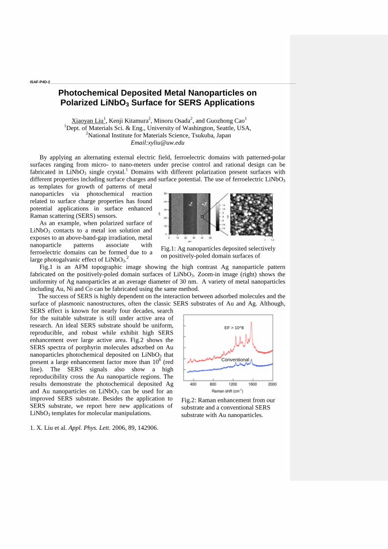
ISAF-P4D-2 _____________________________________________________________________________________________________________________
Photochemical Deposited Metal Nanoparticles on Polarized LiNbO3 Surface for SERS Applications
Xiaoyan Liu
1, Kenji Kitamura
2, Minoru Osada
2, and Guozhong Cao
1
1Dept. of Materials Sci. & Eng., University of Washington, Seattle, USA,
2National Institute for Materials Science, Tsukuba, Japan
Email:[email protected]
By applying an alternating external electric field, ferroelectric domains with patterned-polar
surfaces ranging from micro- to nano-meters under precise control and rational design can be
fabricated in LiNbO3 single crystal.1 Domains with different polarization present surfaces with
different properties including surface charges and surface potential. The use of ferroelectric LiNbO3
as templates for growth of patterns of metal
nanoparticles via photochemical reaction
related to surface charge properties has found
potential applications in surface enhanced
Raman scattering (SERS) sensors.
As an example, when polarized surface of
LiNbO3 contacts to a metal ion solution and
exposes to an above-band-gap irradiation, metal
nanoparticle patterns associate with
ferroelectric domains can be formed due to a
large photogalvanic effect of LiNbO3.2
Fig.1 is an AFM topographic image showing the high contrast Ag nanoparticle pattern
fabricated on the positively-poled domain surfaces of LiNbO3. Zoom-in image (right) shows the
uniformity of Ag nanoparticles at an average diameter of 30 nm. A variety of metal nanoparticles
including Au, Ni and Co can be fabricated using the same method.
The success of SERS is highly dependent on the interaction between adsorbed molecules and the
surface of plasmonic nanostructures, often the classic SERS substrates of Au and Ag. Although,
SERS effect is known for nearly four decades, search
for the suitable substrate is still under active area of
research. An ideal SERS substrate should be uniform,
reproducible, and robust while exhibit high SERS
enhancement over large active area. Fig.2 shows the
SERS spectra of porphyrin molecules adsorbed on Au
nanoparticles photochemical deposited on LiNbO3 that
present a large enhancement factor more than 108 (red
line). The SERS signals also show a high
reproducibility cross the Au nanoparticle regions. The
results demonstrate the photochemical deposited Ag
and Au nanoparticles on LiNbO3 can be used for an
improved SERS substrate. Besides the application to
SERS substrate, we report here new applications of
LiNbO3 templates for molecular manipulations.
1. X. Liu et al. Appl. Phys. Lett. 2006, 89, 142906.
Fig.1: Ag nanoparticles deposited selectively
on positively-poled domain surfaces of
LiNbO3.
EF > 10^8
Conventional
Fig.2: Raman enhancement from our
substrate and a conventional SERS
substrate with Au nanoparticles.

2. X. Liu et al. Appl. Phys. Lett. 2007, 91, 044101.
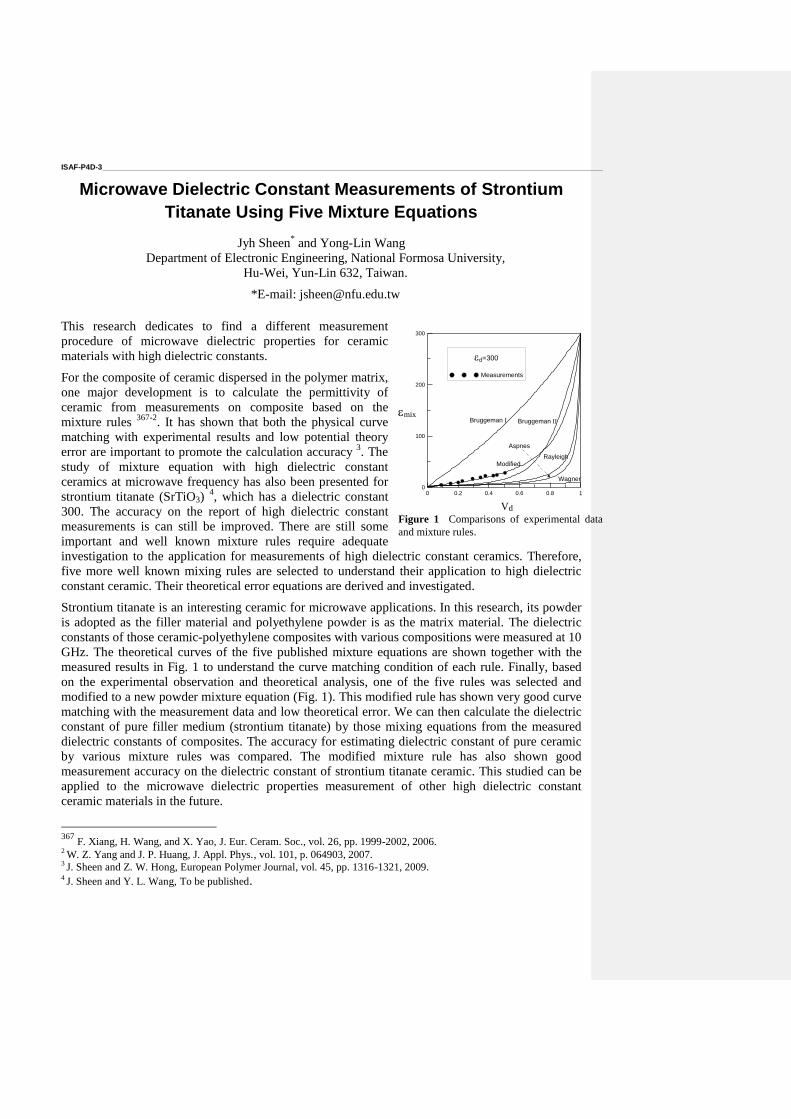
ISAF-P4D-3 _____________________________________________________________________________________________________________________
Microwave Dielectric Constant Measurements of Strontium
Titanate Using Five Mixture Equations
Jyh Sheen* and Yong-Lin Wang
Department of Electronic Engineering, National Formosa University,
Hu-Wei, Yun-Lin 632, Taiwan.
*E-mail: [email protected]
This research dedicates to find a different measurement
procedure of microwave dielectric properties for ceramic
materials with high dielectric constants.
For the composite of ceramic dispersed in the polymer matrix,
one major development is to calculate the permittivity of
ceramic from measurements on composite based on the
mixture rules 367-2
. It has shown that both the physical curve
matching with experimental results and low potential theory
error are important to promote the calculation accuracy 3. The
study of mixture equation with high dielectric constant
ceramics at microwave frequency has also been presented for
strontium titanate (SrTiO3) 4, which has a dielectric constant
300. The accuracy on the report of high dielectric constant
measurements is can still be improved. There are still some
important and well known mixture rules require adequate
investigation to the application for measurements of high dielectric constant ceramics. Therefore,
five more well known mixing rules are selected to understand their application to high dielectric
constant ceramic. Their theoretical error equations are derived and investigated.
Strontium titanate is an interesting ceramic for microwave applications. In this research, its powder
is adopted as the filler material and polyethylene powder is as the matrix material. The dielectric
constants of those ceramic-polyethylene composites with various compositions were measured at 10
GHz. The theoretical curves of the five published mixture equations are shown together with the
measured results in Fig. 1 to understand the curve matching condition of each rule. Finally, based
on the experimental observation and theoretical analysis, one of the five rules was selected and
modified to a new powder mixture equation (Fig. 1). This modified rule has shown very good curve
matching with the measurement data and low theoretical error. We can then calculate the dielectric
constant of pure filler medium (strontium titanate) by those mixing equations from the measured
dielectric constants of composites. The accuracy for estimating dielectric constant of pure ceramic
by various mixture rules was compared. The modified mixture rule has also shown good
measurement accuracy on the dielectric constant of strontium titanate ceramic. This studied can be
applied to the microwave dielectric properties measurement of other high dielectric constant
ceramic materials in the future.
367
F. Xiang, H. Wang, and X. Yao, J. Eur. Ceram. Soc., vol. 26, pp. 1999-2002, 2006. 2
W. Z. Yang and J. P. Huang, J. Appl. Phys., vol. 101, p. 064903, 2007. 3 J. Sheen and Z. W. Hong, European Polymer Journal, vol. 45, pp. 1316-1321, 2009.
4 J. Sheen and Y. L. Wang, To be published.
0 0.2 0.4 0.6 0.8 10
100
200
300
d=300
Measurements
Vd
mix
Aspnes
RayleighModified
Wagner
Bruggeman IIBruggeman I
Figure 1 Comparisons of experimental data
and mixture rules.

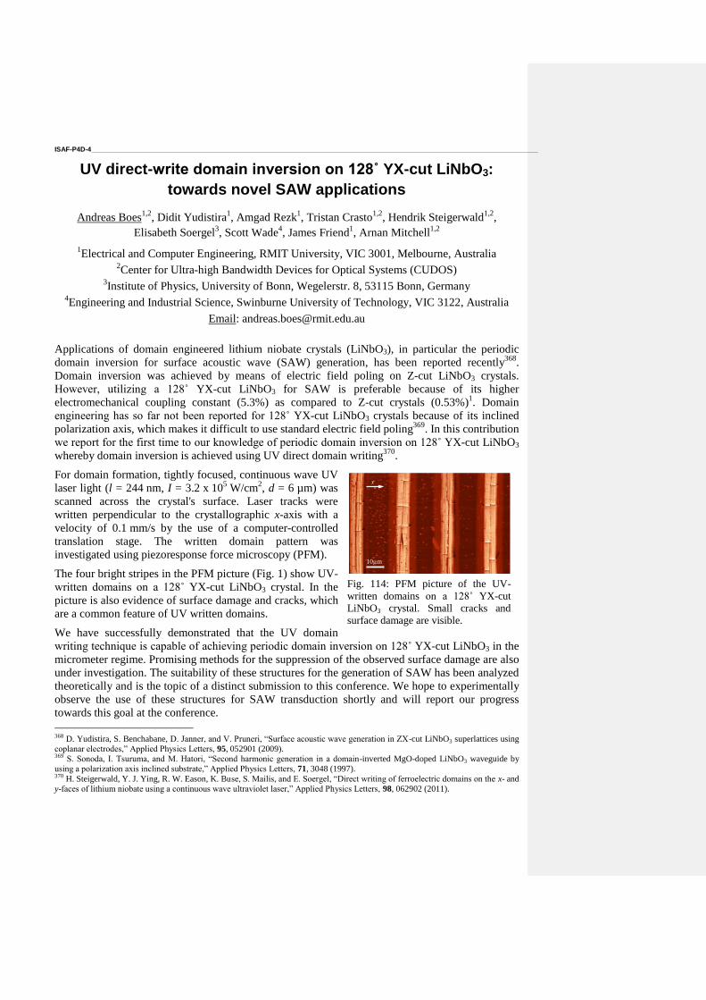
ISAF-P4D-4 _____________________________________________________________________________________________________________________
UV direct-write domain inversion on 128˚ YX-cut LiNbO3:
towards novel SAW applications
Andreas Boes1,2
, Didit Yudistira1, Amgad Rezk
1, Tristan Crasto
1,2, Hendrik Steigerwald
1,2,
Elisabeth Soergel3, Scott Wade
4, James Friend
1, Arnan Mitchell
1,2
1Electrical and Computer Engineering, RMIT University, VIC 3001, Melbourne, Australia
2Center for Ultra-high Bandwidth Devices for Optical Systems (CUDOS)
3Institute of Physics, University of Bonn, Wegelerstr. 8, 53115 Bonn, Germany
4Engineering and Industrial Science, Swinburne University of Technology, VIC 3122, Australia
Email: [email protected]
Applications of domain engineered lithium niobate crystals (LiNbO3), in particular the periodic
domain inversion for surface acoustic wave (SAW) generation, has been reported recently368
.
Domain inversion was achieved by means of electric field poling on Z-cut LiNbO3 crystals.
However, utilizing a 128˚ YX-cut LiNbO3 for SAW is preferable because of its higher
electromechanical coupling constant (5.3%) as compared to Z-cut crystals (0.53%)1. Domain
engineering has so far not been reported for 128˚ YX-cut LiNbO3 crystals because of its inclined
polarization axis, which makes it difficult to use standard electric field poling369
. In this contribution
we report for the first time to our knowledge of periodic domain inversion on 128˚ YX-cut LiNbO3
whereby domain inversion is achieved using UV direct domain writing370
.
For domain formation, tightly focused, continuous wave UV
laser light (l = 244 nm, I = 3.2 x 10⁵ W/cm
2, d = 6 µm) was
scanned across the crystal's surface. Laser tracks were
written perpendicular to the crystallographic x-axis with a
velocity of 0.1 mm/s by the use of a computer-controlled
translation stage. The written domain pattern was
investigated using piezoresponse force microscopy (PFM).
The four bright stripes in the PFM picture (Fig. 1) show UV-
written domains on a 128˚ YX-cut LiNbO3 crystal. In the
picture is also evidence of surface damage and cracks, which
are a common feature of UV written domains.
We have successfully demonstrated that the UV domain
writing technique is capable of achieving periodic domain inversion on 128˚ YX-cut LiNbO3 in the
micrometer regime. Promising methods for the suppression of the observed surface damage are also
under investigation. The suitability of these structures for the generation of SAW has been analyzed
theoretically and is the topic of a distinct submission to this conference. We hope to experimentally
observe the use of these structures for SAW transduction shortly and will report our progress
towards this goal at the conference.
368 D. Yudistira, S. Benchabane, D. Janner, and V. Pruneri, “Surface acoustic wave generation in ZX-cut LiNbO3 superlattices using
coplanar electrodes,” Applied Physics Letters, 95, 052901 (2009). 369 S. Sonoda, I. Tsuruma, and M. Hatori, “Second harmonic generation in a domain-inverted MgO-doped LiNbO3 waveguide by
using a polarization axis inclined substrate,” Applied Physics Letters, 71, 3048 (1997). 370 H. Steigerwald, Y. J. Ying, R. W. Eason, K. Buse, S. Mailis, and E. Soergel, “Direct writing of ferroelectric domains on the x- and
y-faces of lithium niobate using a continuous wave ultraviolet laser,” Applied Physics Letters, 98, 062902 (2011).
10µm
x
Fig. 114: PFM picture of the UV-
written domains on a 128˚ YX-cut
LiNbO3 crystal. Small cracks and
surface damage are visible.
ISAF-P4D-5 _____________________________________________________________________________________________________________________
PLD Elaboration of Piezoelectric ZnO Thin Film for 540 MHz
Al/ZnO/Pt Bulk Acoustic Wave Resonator
Serhane Rafik1, Abdelli-Messaci Samira
1, Lafane Slimane
1, Khales Hammouche
1, Aouimeur
Walid1, Hassein-Bey Abdelkadder
1,2, Boutkedjirt Tarek
3
1 Centre for Development of Advanced Technologies (CDTA). Cité 20 Août 1956, Baba Hassen,
BP: 17, DZ-16303, Algiers, Algeria. 2
Micro & Nano Physics Group, Faculty of Sciences, University Saad Dahlab of Blida (USDB), BP.
270, DZ-09000 Blida. Algeria 3
Equipe de Recherche Physique des Ultrasons, Faculté de physique, Université des Sciences et de
la Technologie Houari Boumediene (USTHB), BP 32, DZ-16111, El-Alia, Bab-Ezzouar,
Algiers. Algeria.
Email: [email protected], [email protected]
ZnO thin films in Al/ZnO/Pt/Ti/SiO2/Si Bulk Acoustic Wave (BAW) resonators are realized by
reactive Pulsed Laser Deposition (PLD) technique. It is of most interest to improve their
piezoelectric characteristics. These later are intimately linked to the texture, the microstructure and
growth conditions. In this work, piezoelectric characteristics of ZnO thin films have been
investigated. The Wurtzite ZnO thin films were prepared on Pt(111) at different substrate
temperatures (100-500 °C) by a reactive PLD technique. The 200 nm of Pt on 20 nm Ti were
prepared by Electron Beam Deposition (EBD) technique at room temperature on 2 µm SiO2
substrate. This SiO2 film has been realized by Silicon wet thermal oxidation step, under (H2+O2)(5
slm+3.5 slm) gas flows at 1100 °C for 9h 10min. The top electrode of the BAW was made by
thermal evaporation of Aluminum; the piezoelectric film was confined in a circle of 1.8 mm radius.
The X-Ray diffraction (XRD) characterization showed that the deposited Pt (bottom electrode) has
(111) preferential orientation. It also showed that the ZnO films were c-axis (002) oriented. The
Scanning Electron Microscopy (SEM) of the realized ZnO thin film showed evidence of compact
grains with honeycomb-like structure on surface and evidence of columnar structure on cross-
section. The measurements indicate that all substrate temperatures are suitable to obtain a good
quality of ZnO, but Ts=300 °C is the optimized one. In order to evaluate the piezoelectric properties
of the BAW, measurements of the electrical input impedance and admittance have been performed.
They showed evidence of piezoelectric response. The resonance frequency was obtained at 524.5
MHz and the anti-resonance frequency at 540.9 MHz. The values of quality factors were
respectively; Qr=1125.6 and Qa=856.51. The electromechanical coupling coefficient was evaluated
at Keff2=7.26 %, which is an indicator of a good piezoelectric response. From this measured values,
the thickness and wave velocity in the ZnO slab were deduced to be (d = 6.15 µm and Vp = 6451.35
m/s) and the piezoelectric constant e33 was found to be equal to 1.21 C/m2.
ISAF-P4D-6 _____________________________________________________________________________________________________________________
Ferroelectric Liquid Crystals for Display and Photonics
Applications
Vladimir Chigrinov
Hong Kong University of Science and Technology,
Clear Water Bay, Kowloon, Hong Kong
Email: [email protected]
Ferroelectric liquid crystals (FLC) is a good candidate for the new generation display and
photonics devices with advanced performance in comparison with usually used nematic LC. Several
electrooptical modes can be used for for the new generation of FLC devices for displays and
photonics [1]: (i) deformed helix ferroelectric (DHF) effect; (ii) electrically suppressed helix
ferroelectric liquid crystals (ESHFLC); (iii) modulation of light in diffraction FLC grating; and (iv)
orientational electro-optic Kerr effect.
The novel FLC devices may include field sequential color (FSC) FLC with a high resolution, low
power consumption and extended color gamut, which can be used in the screens of portable PCs,
mobile phones, PDAs and micro and pico-projectors.
FLC photonics devices have found applications for the generation of digital holograms, adaptive
beam steering systems, sensors and polarization gratings. Additionally, high-speed communication
systems, producing elements (such as switches, attenuators, polarization rotators) demand FLC
devices with extremely fast response, stable, low loss, operable over a wide temperature range, and
that require small operating voltages and extremely low power consumption.
[1] Vladimir Chigrinov, Eugene Pozhidaev, Abhishek Srivastava, Guo Qi, Ma Ying, Hoi Sing
Kwok, Fast Ferroelectric Liquid Crystal Modes Based on Photoaligning Technology, SID 2013,
Vancouver, Canada, May 2013.
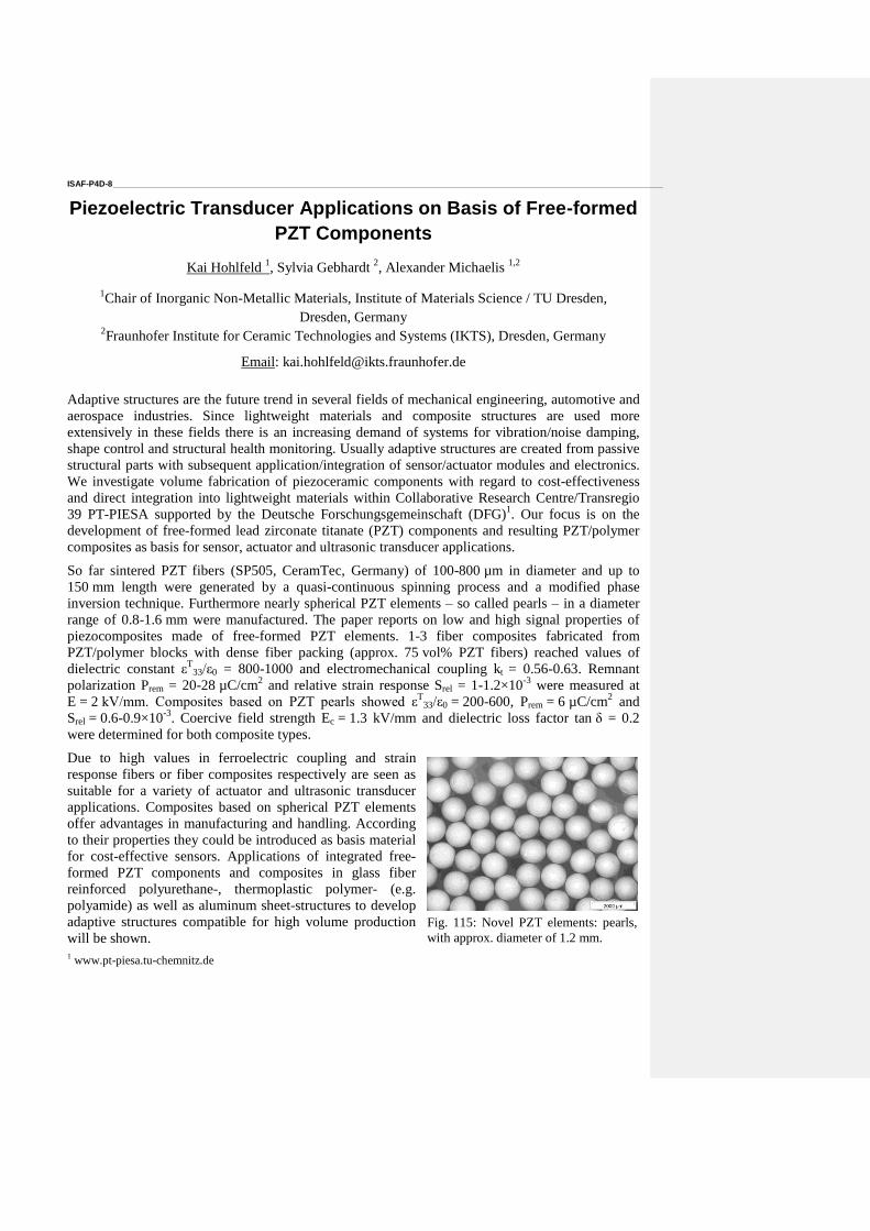
ISAF-P4D-8 _____________________________________________________________________________________________________________________
Piezoelectric Transducer Applications on Basis of Free-formed
PZT Components
Kai Hohlfeld 1, Sylvia Gebhardt
2, Alexander Michaelis
1,2
1Chair of Inorganic Non-Metallic Materials, Institute of Materials Science / TU Dresden,
Dresden, Germany 2Fraunhofer Institute for Ceramic Technologies and Systems (IKTS), Dresden, Germany
Email: [email protected]
Adaptive structures are the future trend in several fields of mechanical engineering, automotive and
aerospace industries. Since lightweight materials and composite structures are used more
extensively in these fields there is an increasing demand of systems for vibration/noise damping,
shape control and structural health monitoring. Usually adaptive structures are created from passive
structural parts with subsequent application/integration of sensor/actuator modules and electronics.
We investigate volume fabrication of piezoceramic components with regard to cost-effectiveness
and direct integration into lightweight materials within Collaborative Research Centre/Transregio
39 PT-PIESA supported by the Deutsche Forschungsgemeinschaft (DFG)1. Our focus is on the
development of free-formed lead zirconate titanate (PZT) components and resulting PZT/polymer
composites as basis for sensor, actuator and ultrasonic transducer applications.
So far sintered PZT fibers (SP505, CeramTec, Germany) of 100-800 µm in diameter and up to
150 mm length were generated by a quasi-continuous spinning process and a modified phase
inversion technique. Furthermore nearly spherical PZT elements – so called pearls – in a diameter
range of 0.8-1.6 mm were manufactured. The paper reports on low and high signal properties of
piezocomposites made of free-formed PZT elements. 1-3 fiber composites fabricated from
PZT/polymer blocks with dense fiber packing (approx. 75 vol% PZT fibers) reached values of
dielectric constant εT
33/ε0 = 800-1000 and electromechanical coupling kt = 0.56-0.63. Remnant
polarization Prem = 20-28 µC/cm2 and relative strain response Srel = 1-1.2×10
-3 were measured at
E = 2 kV/mm. Composites based on PZT pearls showed εT
33/ε0 = 200-600, Prem = 6 µC/cm2 and
Srel = 0.6-0.9×10⁻³
. Coercive field strength Ec = 1.3 kV/mm and dielectric loss factor tan δ = 0.2
were determined for both composite types.
Due to high values in ferroelectric coupling and strain
response fibers or fiber composites respectively are seen as
suitable for a variety of actuator and ultrasonic transducer
applications. Composites based on spherical PZT elements
offer advantages in manufacturing and handling. According
to their properties they could be introduced as basis material
for cost-effective sensors. Applications of integrated free-
formed PZT components and composites in glass fiber
reinforced polyurethane-, thermoplastic polymer- (e.g.
polyamide) as well as aluminum sheet-structures to develop
adaptive structures compatible for high volume production
will be shown. 1 www.pt-piesa.tu-chemnitz.de
Fig. 115: Novel PZT elements: pearls,
with approx. diameter of 1.2 mm.

ISAF-P4D-9 _____________________________________________________________________________________________________________________
Enhanced Electrocaloric Effect in Novel Lead-Free Relaxor
Ferroelectrics.
Florian Le Goupil1, Andrey Berenov
1, Anna-Karin Axelsson
1, Matjaz Valant
2 and Neil McN.
Alford1
1Department of Materials, Imperial College London, London, United Kingdom
2Materials Research Laboratory, University of Nova Gorica, Nova Gorica, Slovenia
Email: [email protected]
In polar crystals the spontaneous polarization increases with application of an external electric field.
Under adiabatic conditions, the system compensates this alignment of dipoles with an increase in
temperature, in order to keep the overall entropy of the system constant. This phenomenon is called
the electrocaloric effect (ECE). The need for more efficient and environmentally-friendly materials
in the refrigeration industry has lead to a significant effort towards the discovery of materials that
exhibit a pronounced EC effect.
We have constructed a direct ECE measurement system, based on a modified-Differential Scanning
Calorimeter (DSC), allowing the acquisition of both thermal (ECE, heat capacity) and electrical (P-
E loops, leakage current) information simultaneously. The ECE of several novel lead-free relaxor
ferroelectric have been measured, including perovskites (substituted BaTiO3), Aurivillius phases
(substituted SrBi2Ta2O9) and tungsten bronzes (SrxBa(1-x)Nb2O6). For most of these systems, the
direct ECE measurements presented here are the first ever reported. It is shown that, most definitely
due to their polar nano-regions, relaxor ferroelectrics experience a second ECE peak, sometimes far
above the temperature of the ferroelectric phase transition, which could provide the wide
temperature range that is required to establish a solid-state electrocaloric cooling cycle.
Comparisons between direct and indirect measurements, obtained from dielectric polarization
measurements versus electric field and temperature, have also been performed on these systems.
Contrary to what we reported for normal ferroelectrics371
, we found large discrepancies between
both methods above the ferroelectric phase transition, in both trend and absolute values. This result
highlights the significant limitations of the indirect ECE method, especially in the case of relaxor
ferroelectrics.
371
F. Le Goupil, A. Berenov, A. Axelsson, M. Valant, and N. M. Alford “Direct and indirect electrocaloric
measurements on <001>-PbMg1/3Nb2/3O3-30PbTiO3 single crystals”, J. Appl. Phys., vol. 111, p. 124109, 2012.
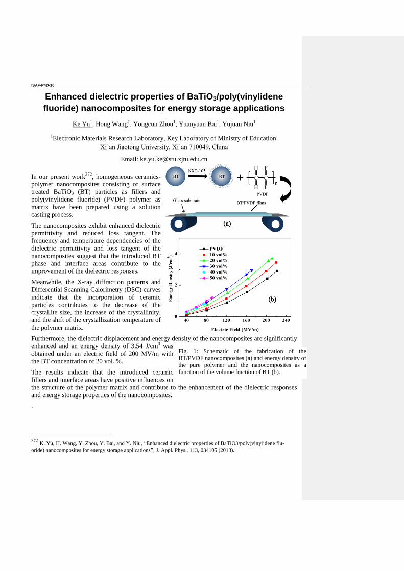
ISAF-P4D-10 ____________________________________________________________________________________________________________________
Enhanced dielectric properties of BaTiO3/poly(vinylidene
fluoride) nanocomposites for energy storage applications
Ke Yu1, Hong Wang
1, Yongcun Zhou
1, Yuanyuan Bai
1, Yujuan Niu
1
1Electronic Materials Research Laboratory, Key Laboratory of Ministry of Education,
Xi’an Jiaotong University, Xi’an 710049, China
Email: [email protected]
In our present work372
, homogeneous ceramics-
polymer nanocomposites consisting of surface
treated BaTiO3 (BT) particles as fillers and
poly(vinylidene fluoride) (PVDF) polymer as
matrix have been prepared using a solution
casting process.
The nanocomposites exhibit enhanced dielectric
permittivity and reduced loss tangent. The
frequency and temperature dependencies of the
dielectric permittivity and loss tangent of the
nanocomposites suggest that the introduced BT
phase and interface areas contribute to the
improvement of the dielectric responses.
Meanwhile, the X-ray diffraction patterns and
Differential Scanning Calorimetry (DSC) curves
indicate that the incorporation of ceramic
particles contributes to the decrease of the
crystallite size, the increase of the crystallinity,
and the shift of the crystallization temperature of
the polymer matrix.
Furthermore, the dielectric displacement and energy density of the nanocomposites are significantly
enhanced and an energy density of 3.54 J/cm3 was
obtained under an electric field of 200 MV/m with
the BT concentration of 20 vol. %.
The results indicate that the introduced ceramic
fillers and interface areas have positive influences on
the structure of the polymer matrix and contribute to the enhancement of the dielectric responses
and energy storage properties of the nanocomposites.
.
372
K. Yu, H. Wang, Y. Zhou, Y. Bai, and Y. Niu, “Enhanced dielectric properties of BaTiO3/poly(vinylidene flu-
oride) nanocomposites for energy storage applications”, J. Appl. Phys., 113, 034105 (2013).
Fig. 1: Schematic of the fabrication of the
BT/PVDF nanocomposites (a) and energy density of
the pure polymer and the nanocomposites as a
function of the volume fraction of BT (b).
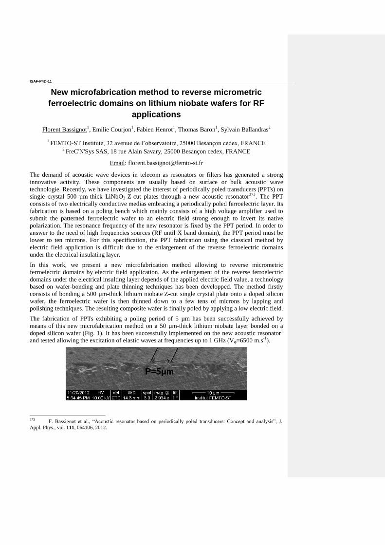
ISAF-P4D-11 ____________________________________________________________________________________________________________________
New microfabrication method to reverse micrometric
ferroelectric domains on lithium niobate wafers for RF
applications
Florent Bassignot1, Emilie Courjon
1, Fabien Henrot
1, Thomas Baron
1, Sylvain Ballandras
2
1 FEMTO-ST Institute, 32 avenue de l’observatoire, 25000 Besançon cedex, FRANCE
2 FreC'N'Sys SAS, 18 rue Alain Savary, 25000 Besançon cedex, FRANCE
Email: [email protected]
The demand of acoustic wave devices in telecom as resonators or filters has generated a strong
innovative activity. These components are usually based on surface or bulk acoustic wave
technologie. Recently, we have investigated the interest of periodically poled transducers (PPTs) on
single crystal 500 µm-thick LiNbO3 Z-cut plates through a new acoustic resonator373
. The PPT
consists of two electrically conductive medias embracing a periodically poled ferroelectric layer. Its
fabrication is based on a poling bench which mainly consists of a high voltage amplifier used to
submit the patterned ferroelectric wafer to an electric field strong enough to invert its native
polarization. The resonance frequency of the new resonator is fixed by the PPT period. In order to
answer to the need of high frequencies sources (RF until X band domain), the PPT period must be
lower to ten microns. For this specification, the PPT fabrication using the classical method by
electric field application is difficult due to the enlargement of the reverse ferroelectric domains
under the electrical insulating layer.
In this work, we present a new microfabrication method allowing to reverse micrometric
ferroelectric domains by electric field application. As the enlargement of the reverse ferroelectric
domains under the electrical insulting layer depends of the applied electric field value, a technology
based on wafer-bonding and plate thinning techniques has been developped. The method firstly
consists of bonding a 500 µm-thick lithium niobate Z-cut single crystal plate onto a doped silicon
wafer, the ferroelectric wafer is then thinned down to a few tens of microns by lapping and
polishing techniques. The resulting composite wafer is finally poled by applying a low electric field.
The fabrication of PPTs exhibiting a poling period of 5 µm has been successfully achieved by
means of this new microfabrication method on a 50 µm-thick lithium niobate layer bonded on a
doped silicon wafer (Fig. 1). It has been successfully implemented on the new acoustic resonator1
and tested allowing the excitation of elastic waves at frequencies up to 1 GHz (Vφ=6500 m.s-1
).
373
F. Bassignot et al., “Acoustic resonator based on periodically poled transducers: Concept and analysis”, J.
Appl. Phys., vol. 111, 064106, 2012.

Fig. 116: SEM view of a 5 µm period device based on a doped silicon plate bonded on a 50 µm-thick lithium
niobate layer. The structure has been etched in a hydrogen fluoride solution in order to observe the domain
alternation.
ISAF-P4D-12 ____________________________________________________________________________________________________________________
BZN Thin-Film Multilayer Capacitors Fabricated at Low
Temperature by Radio Frequency Magnetron Sputtering
Fan He, Saeed Khan, Wei Ren*, Peng Shi, and Xiaoqing Wu
Electronic Materials Research Laboratory, Key Laboratory of the Ministry of Education &
International Center for Dielectric Research, Xi’an Jiaotong University, Xi’an 710049, China
* Email: [email protected]
In this study, thin film multilayered capacitors (MLCs) composed of amorphous Bi1.5Zn1.0Nb1.5O7
(BZN) dielectric layers with internal electrodes were fabricated by radio-frequency (RF) sputtering
at a temperature below 150 C. All BZN thin films were deposited through a set of steel shadow
masks at room temperature and post-annealed at 150 C. XRD pattern and SEM images confirmed
that the BZN dielectric layers used in these MLCs are amorphous and the thickness for each BZN
layer is approximately 200 nm. Metallic Pt and Cu with about 50 nm thick were studied as internal
electrodes, respectively. We fabricated BZN thin film MLCs with different layers. The thin film
MLCs with 5 BZN layers exhibit promising dielectric properties: the relative permittivity of around
60, the dielectric loss of 13% at 10 kHz and a leakage current of 10
-4 A at a dc bias electric field of
150 kV/cm. The capacitance density for each dielectric layer is around 300 nF/cm2. The BZN thin
film MLCs have a potential application on embedded PCBs.
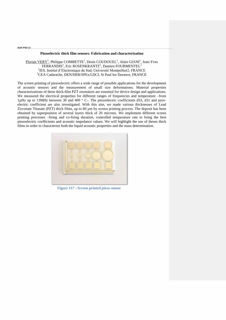
ISAF-P4D-13 ____________________________________________________________________________________________________________________
Piezoelectric thick film sensors: Fabrication and characterization
Florian VERY1, Philippe COMBETTE
1, Denis COUDOUEL
1, Alain GIANI
1, Jean-Yves
FERRANDIS1, Eric ROSENKRANTZ
1, Damien FOURMENTEL
2
1IES, Institut d’Electronique du Sud, Université Montpellier2, FRANCE
2CEA Cadarache, DEN/DER/SPEx/LDCI, St Paul lez Durance, FRANCE
The screen printing of piezoelectric offers a wide range of possible applications for the development
of acoustic sensors and the measurement of small size deformations. Material properties
characterizations of these thick-film PZT resonators are essential for device design and applications.
We measured the electrical properties for different ranges of frequencies and temperature –from
1µHz up to 13MHz between 30 and 400 ° C-. The piezoelectric coefficients d33, d31 and pyro-
electric coefficient are also investigated. With this aim, we made various thicknesses of Lead
Zirconate Titanate (PZT) thick films, up to 60 µm by screen printing process. The deposit has been
obtained by superposition of several layers thick of 20 microns. We implement different screen
printing processes –firing and co-firing duration, controlled temperature rate to bring the best
piezoelectric coefficients and acoustic impedance values. We will highlight the use of theses thick
films in order to characterize both the liquid acoustic properties and the mass determination.
Figure 117 : Screen printed piezo sensor
ISAF-P4D-14 ____________________________________________________________________________________________________________________
Multi-physical numerical modeling of a piezoelectric
loudspeaker for hearing aid applications and experimental
validation
Gustavo C. Martins1, Leonardo Seki
1, Júlio A. Cordioli
1
1Department of Mechanical Engineering, Federal University of Santa Catarina, Florianópolis, Brazil
Email: [email protected]
Piezoelectric materials are widely used in applications involving miniaturized components. The
application of these materials in hearing aid receivers presents technical and economic advantages
such as reducing the number of parts of the system and its manufacturing cost. The modeling of a
miniaturized piezoelectric loudspeaker for hearing aids involves multi-physical models with strong
coupling between the involved physics. In the literature, analytical models of these components can
be found. However, these analytical models usually involve very simple geometries and boundary
conditions. These characteristics restrict the use of such models as a design tool for miniaturized
piezoelectric loudspeaker analysis. This work presents multi-physical numerical models of
miniaturized loudspeaker prototypes. The numerical models were constructed using the Finite
Element Method (FEM). The loudspeakers are composed of a piezoelectric diaphragm coupled to
small cavities with different depths, and the multi-physical model includes the coupled
piezoelectric, structural and acoustic behaviors of the systems. For the cavity with reduced depth,
thermal and viscous effects on the acoustic propagation are taken in account in the FEM model.
Finally, experimental tests of the piezoelectric diaphragm alone and coupled with the acoustic
cavities are used to validate the multi-physical model.
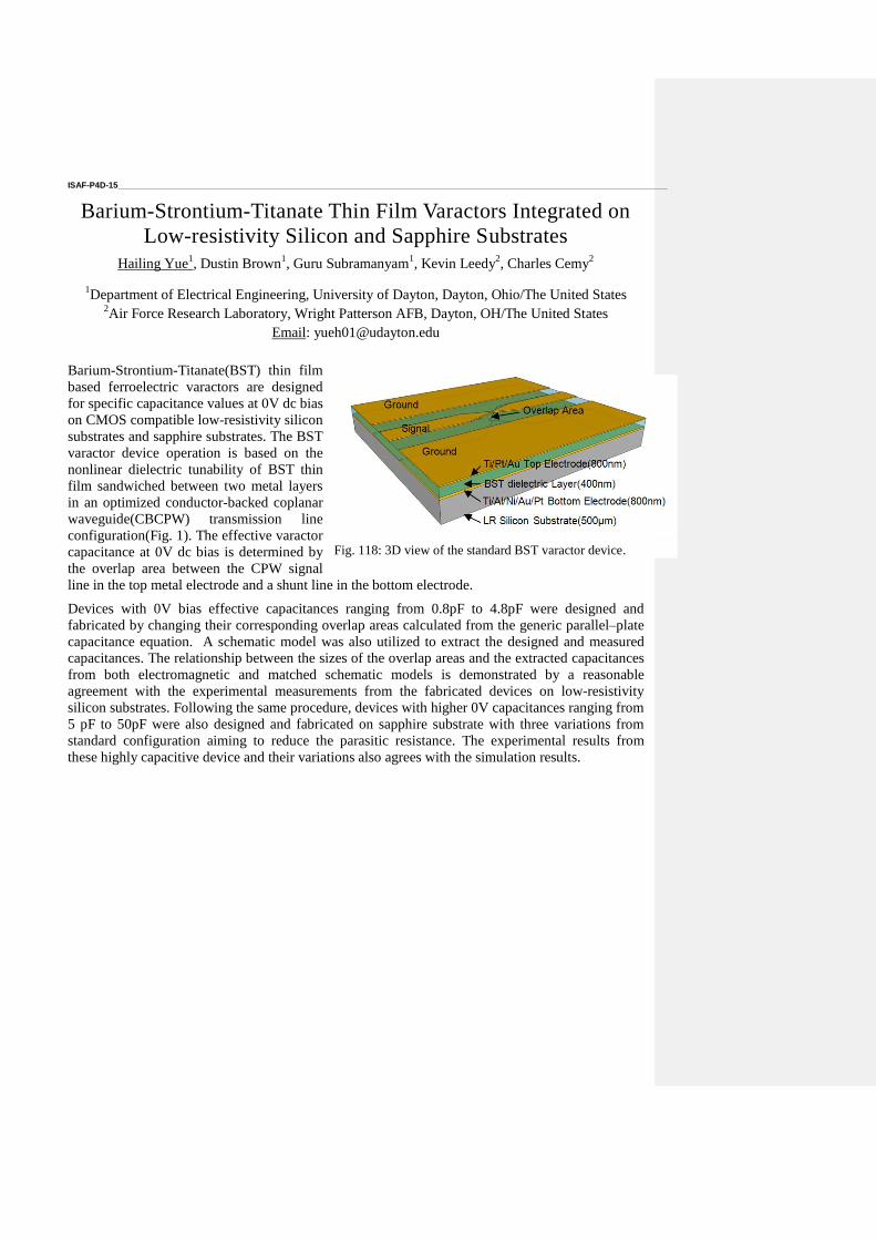
ISAF-P4D-15 ____________________________________________________________________________________________________________________
Barium-Strontium-Titanate Thin Film Varactors Integrated on
Low-resistivity Silicon and Sapphire Substrates
Hailing Yue1, Dustin Brown
1, Guru Subramanyam
1, Kevin Leedy
2, Charles Cemy
2
1Department of Electrical Engineering, University of Dayton, Dayton, Ohio/The United States
2Air Force Research Laboratory, Wright Patterson AFB, Dayton, OH/The United States
Email: [email protected]
Barium-Strontium-Titanate(BST) thin film
based ferroelectric varactors are designed
for specific capacitance values at 0V dc bias
on CMOS compatible low-resistivity silicon
substrates and sapphire substrates. The BST
varactor device operation is based on the
nonlinear dielectric tunability of BST thin
film sandwiched between two metal layers
in an optimized conductor-backed coplanar
waveguide(CBCPW) transmission line
configuration(Fig. 1). The effective varactor
capacitance at 0V dc bias is determined by
the overlap area between the CPW signal
line in the top metal electrode and a shunt line in the bottom electrode.
Devices with 0V bias effective capacitances ranging from 0.8pF to 4.8pF were designed and
fabricated by changing their corresponding overlap areas calculated from the generic parallel–plate
capacitance equation. A schematic model was also utilized to extract the designed and measured
capacitances. The relationship between the sizes of the overlap areas and the extracted capacitances
from both electromagnetic and matched schematic models is demonstrated by a reasonable
agreement with the experimental measurements from the fabricated devices on low-resistivity
silicon substrates. Following the same procedure, devices with higher 0V capacitances ranging from
5 pF to 50pF were also designed and fabricated on sapphire substrate with three variations from
standard configuration aiming to reduce the parasitic resistance. The experimental results from
these highly capacitive device and their variations also agrees with the simulation results.
Fig. 118: 3D view of the standard BST varactor device.
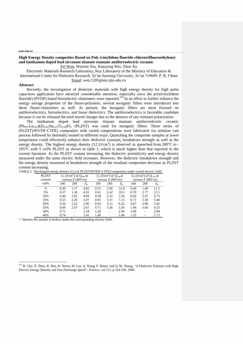
ISAF-P4D-16 ____________________________________________________________________________________________________________________
High Energy Density composites Based on Poly (vinylidene fluoride-chlorotrifluoroethylene)
and lanthanum doped lead zirconate titanate stannate antiferroelectric ceramic
Fei Wen, Weimin Xia, Xiaoyong Wei, Zhuo Xu
Electronic Materials Research Laboratory, Key Laboratory of the Ministry of Education &
International Center for Dielectric Research, Xi’an Jiaotong University, Xi’an 710049. P. R. China
Email: [email protected]
Abstract
Recently, the investigation of dielectric materials with high energy density for high pulse
capacitors application have attracted considerable attention, especially since the poly(vinylidene
fluoride) (PVDF) based ferroelectric elastomers were reported.374
In an effort to further enhance the
energy storage properties of the fluoro-polymers, several inorganic fillers were introduced into
these fluoro-elastomers as well. At present, the inorganic fillers are most focused on
antiferroelectrics, ferroelectrics, and linear dielectrics. The antiferroelectrics is favorable candidate
because it can be released the total stored charges due to the absence of any remnant polarization.
The lanthanum doped lead zirconate titanate stannate antiferroelectric ceramic
(Pb0.97La0.02)(Zr0.65Sn0.25Ti0.10)O3 (PLZST) was used for inorganic fillers. Three series of
(PLZST)/P(VDF-CTFE) composites with varied compositions were fabricated via solution cast
process followed by thermally treated in different ways. Quenching the composite samples at lower
temperature could effectively enhance their dielectric constant, breakdown strength as well as the
energy density. The highest energy density (12.1J/cm3) is observed in quenched from 200°C to -
195°C with 5 vol% PLZST as shown in table 1, which is much higher than that reported in the
current literature. As the PLZST content increasing, the dielectric permittivity and energy density
measured under the same electric field increases. However, the dielectric breakdown strength and
the energy density measured at breakdown strength of the resultant composites decrease as PLZST
content increasing.
TABLE I. Discharged energy density (Ue) of PLZST/P(VDF-CTFE) composites under varied electric field.
PLZST
content
vol%
Ue (J/cm3) of Q100 at
various E (MV/m)
Ue (J/cm3) of Q-94 at
various E (MV/m)
Ue (J/cm3) of Q-195 at
various E (MV/m)
100 200 Eb 100 200 Eb 100 200 Eb
0 0.30 1.17 4.82 0.51 2.06 12.4 0.40 1.69 11.3
5% 0.37 1.38 4.10 0.61 2.42 10.5 0.70 2.77 12.1
10% 0.46 1.81 4.84 0.58 2.32 7.56 0.62 2.47 5.73
15% 0.55 2.26 5.07 0.81 3.11 7.15 0.71 2.58 5.40
20% 0.56 2.22 2.96 0.93 3.11 6.22 0.67 2.80 3.42
25% 0.69 2.47 2.67 0.71 3.26 3.26 1.06 3.60 4.25
30% 0.71 - 2.18 1.20 - 2.94 1.09 - 2.84
40% 0.74 - 1.41 1.46 - 2.46 1.35 - 2.72
“-”denotes the sample is broken under the corresponding electric field.
374
B. Chu, X. Zhou, K. Ren, B. Neese, M. Lin, Q. Wang, F. Bauer, and Q. M. Zhang, “A Dielectric Polymer with High
Electric Energy Density and Fast Discharge Speed”, Science, vol.313, p.334-336, 2006.

ISAF-P4D-17 ____________________________________________________________________________________________________________________
Flexible Piezoelectric Energy Harvesters Fabricated by KNbO3
Nanowires
Mi-Ri Joung1, Haibo Xu
1, Jin-Seong Kim
1, In-Tae Seo
1, Sahn Nahm
1,2, Seok-Jin Yoon
3, Chong-
Yun Kang2,3
1Department of Materials Science and Engineering, Korea University, Seoul, Korea
2Department of Information Technology-Nano Science, Korea University-Korea Institute of
Science and Technology School, Korea University, Seoul, Korea 3Electronic Materials Center, Korea Institute of Science and Technology, Seoul, Korea
Email: [email protected]
Tetragonal KNbO3 (KN) nanowires were formed when the synthesis was carried out at 120oC for 48
h. However, when the fabrication was conducted at high temperatures (≥ 150oC) or at 120
oC for a
long period of time (≥ 72 h), orthorhombic KN nanowires were obtained. Moreover, the KN
nanowires synthesized at 120oC for 60 h showed a morphotropic phase boundary (MPB) structure
in which both tetragonal and orthorhombic structures coexisted. A tetragonal KN nanowire
exhibited a d33 value of 137.1 pm/V, which is larger than that of the orthorhombic KN nanowire
(104.5 pm/V), probably because of the softening effect of the metal vacancies. The MPB KN
nanowires exhibited a larger d33 value of 146.0 pm/V. Three types of the KN nanowires were mixed
with Polydimethylsiloxane(PDMS) and these mixtures (PDMS-KN) were deposited on the Au-
coated Polyimide(PI) substrate. Finally, the Au-coated PI was covered on the PI/Au/PDMS-KN
device to fabricate the piezoelectric energy havrester. In these work, three types of KN piezoelectric
energy harvesters were fabricated and the output power of these harvesters were investigated.
Moreover, the magnitude of their output power was explained based on the structural and
piezoelectric prperties of the KN nanowires.
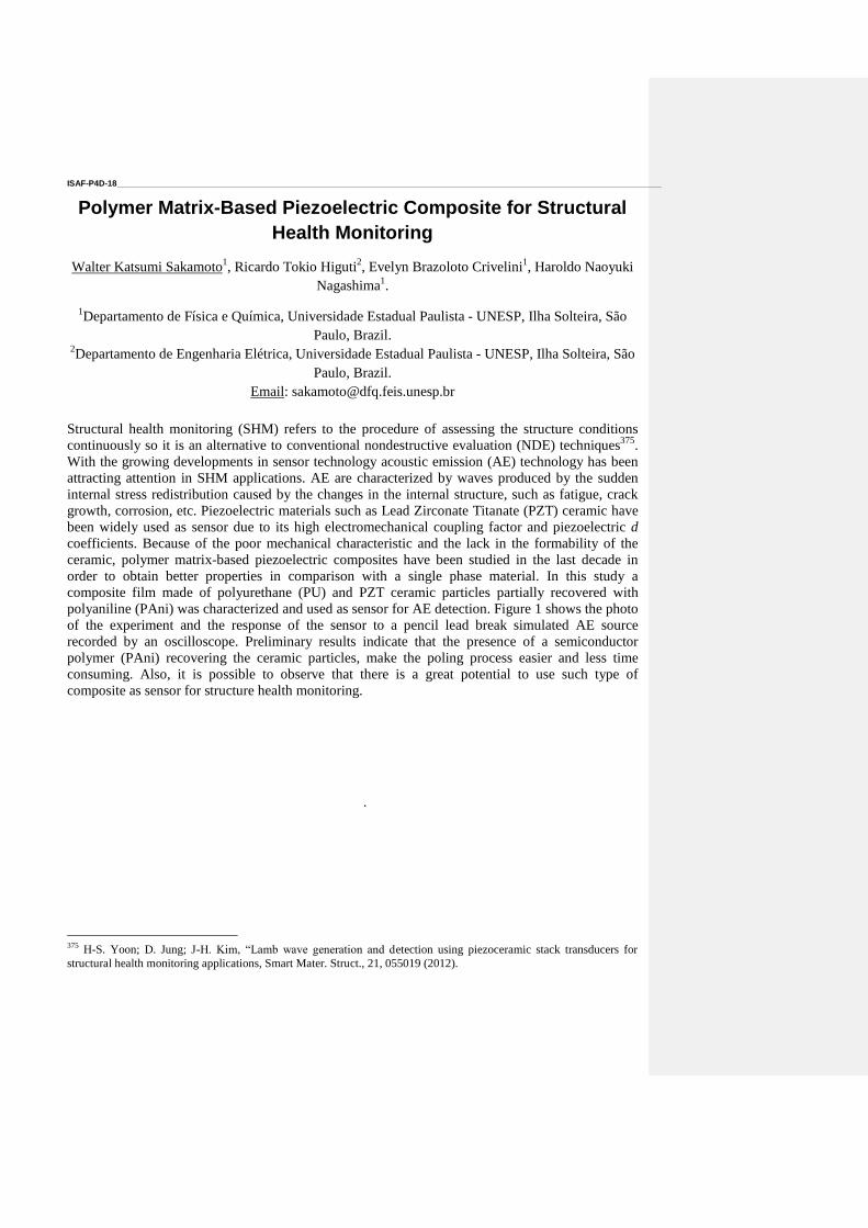
ISAF-P4D-18 ____________________________________________________________________________________________________________________
Polymer Matrix-Based Piezoelectric Composite for Structural
Health Monitoring
Walter Katsumi Sakamoto1, Ricardo Tokio Higuti
2, Evelyn Brazoloto Crivelini
1, Haroldo Naoyuki
Nagashima1.
1Departamento de Física e Química, Universidade Estadual Paulista - UNESP, Ilha Solteira, São
Paulo, Brazil. 2Departamento de Engenharia Elétrica, Universidade Estadual Paulista - UNESP, Ilha Solteira, São
Paulo, Brazil.
Email: [email protected]
Structural health monitoring (SHM) refers to the procedure of assessing the structure conditions
continuously so it is an alternative to conventional nondestructive evaluation (NDE) techniques375
.
With the growing developments in sensor technology acoustic emission (AE) technology has been
attracting attention in SHM applications. AE are characterized by waves produced by the sudden
internal stress redistribution caused by the changes in the internal structure, such as fatigue, crack
growth, corrosion, etc. Piezoelectric materials such as Lead Zirconate Titanate (PZT) ceramic have
been widely used as sensor due to its high electromechanical coupling factor and piezoelectric d
coefficients. Because of the poor mechanical characteristic and the lack in the formability of the
ceramic, polymer matrix-based piezoelectric composites have been studied in the last decade in
order to obtain better properties in comparison with a single phase material. In this study a
composite film made of polyurethane (PU) and PZT ceramic particles partially recovered with
polyaniline (PAni) was characterized and used as sensor for AE detection. Figure 1 shows the photo
of the experiment and the response of the sensor to a pencil lead break simulated AE source
recorded by an oscilloscope. Preliminary results indicate that the presence of a semiconductor
polymer (PAni) recovering the ceramic particles, make the poling process easier and less time
consuming. Also, it is possible to observe that there is a great potential to use such type of
composite as sensor for structure health monitoring.
375
H-S. Yoon; D. Jung; J-H. Kim, “Lamb wave generation and detection using piezoceramic stack transducers for
structural health monitoring applications, Smart Mater. Struct., 21, 055019 (2012).
.
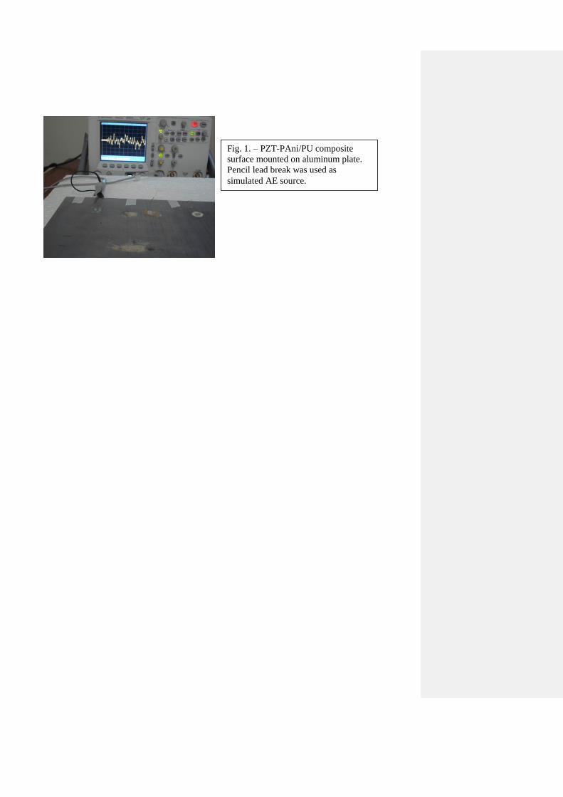
Fig. 1. – PZT-PAni/PU composite
surface mounted on aluminum plate.
Pencil lead break was used as
simulated AE source.
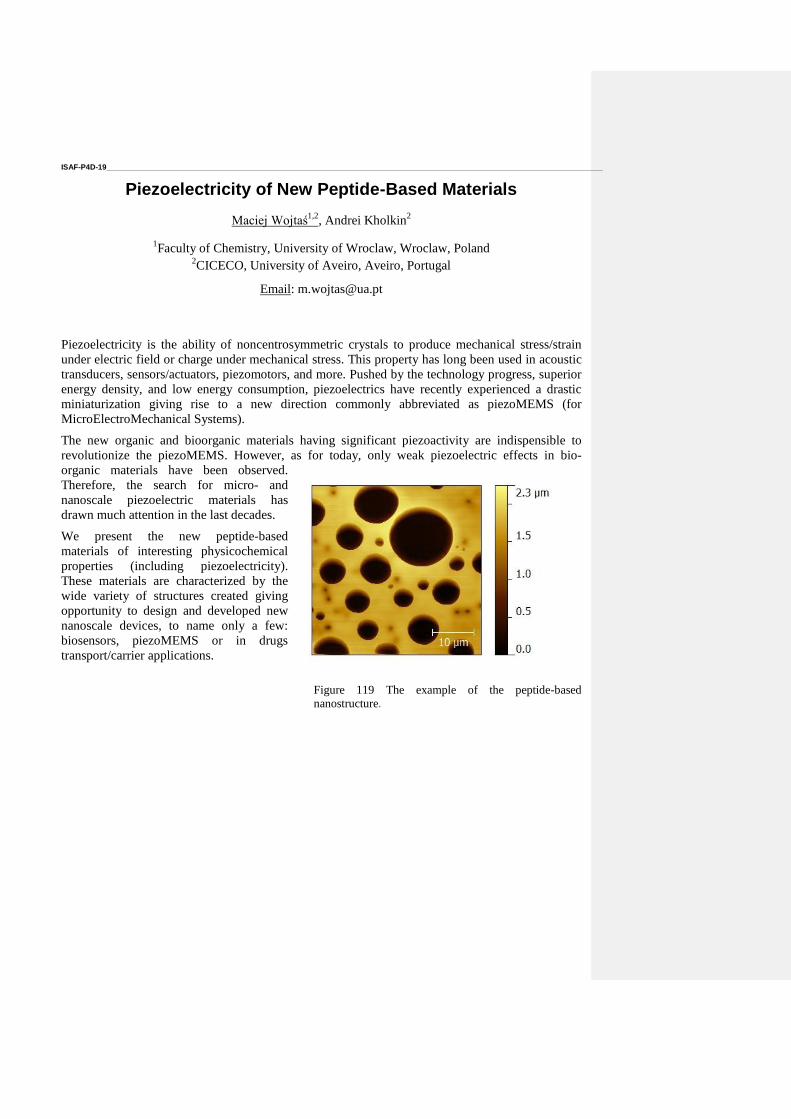
ISAF-P4D-19 ____________________________________________________________________________________________________________________
Piezoelectricity of New Peptide-Based Materials
Maciej Wojtaś1,2
, Andrei Kholkin2
1Faculty of Chemistry, University of Wroclaw, Wroclaw, Poland
2CICECO, University of Aveiro, Aveiro, Portugal
Email: [email protected]
Piezoelectricity is the ability of noncentrosymmetric crystals to produce mechanical stress/strain
under electric field or charge under mechanical stress. This property has long been used in acoustic
transducers, sensors/actuators, piezomotors, and more. Pushed by the technology progress, superior
energy density, and low energy consumption, piezoelectrics have recently experienced a drastic
miniaturization giving rise to a new direction commonly abbreviated as piezoMEMS (for
MicroElectroMechanical Systems).
The new organic and bioorganic materials having significant piezoactivity are indispensible to
revolutionize the piezoMEMS. However, as for today, only weak piezoelectric effects in bio-
organic materials have been observed.
Therefore, the search for micro- and
nanoscale piezoelectric materials has
drawn much attention in the last decades.
We present the new peptide-based
materials of interesting physicochemical
properties (including piezoelectricity).
These materials are characterized by the
wide variety of structures created giving
opportunity to design and developed new
nanoscale devices, to name only a few:
biosensors, piezoMEMS or in drugs
transport/carrier applications.
Figure 119 The example of the peptide-based
nanostructure.
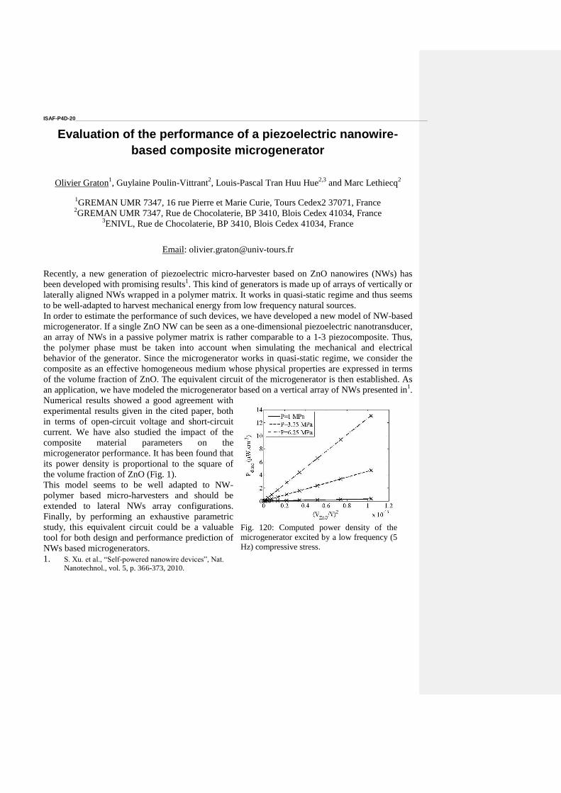
ISAF-P4D-20 ____________________________________________________________________________________________________________________
Evaluation of the performance of a piezoelectric nanowire-
based composite microgenerator
Olivier Graton1, Guylaine Poulin-Vittrant
2, Louis-Pascal Tran Huu Hue
2,3 and Marc Lethiecq
2
1GREMAN UMR 7347, 16 rue Pierre et Marie Curie, Tours Cedex2 37071, France
2GREMAN UMR 7347, Rue de Chocolaterie, BP 3410, Blois Cedex 41034, France
3ENIVL, Rue de Chocolaterie, BP 3410, Blois Cedex 41034, France
Email: [email protected]
Recently, a new generation of piezoelectric micro-harvester based on ZnO nanowires (NWs) has
been developed with promising results1. This kind of generators is made up of arrays of vertically or
laterally aligned NWs wrapped in a polymer matrix. It works in quasi-static regime and thus seems
to be well-adapted to harvest mechanical energy from low frequency natural sources.
In order to estimate the performance of such devices, we have developed a new model of NW-based
microgenerator. If a single ZnO NW can be seen as a one-dimensional piezoelectric nanotransducer,
an array of NWs in a passive polymer matrix is rather comparable to a 1-3 piezocomposite. Thus,
the polymer phase must be taken into account when simulating the mechanical and electrical
behavior of the generator. Since the microgenerator works in quasi-static regime, we consider the
composite as an effective homogeneous medium whose physical properties are expressed in terms
of the volume fraction of ZnO. The equivalent circuit of the microgenerator is then established. As
an application, we have modeled the microgenerator based on a vertical array of NWs presented in1.
Numerical results showed a good agreement with
experimental results given in the cited paper, both
in terms of open-circuit voltage and short-circuit
current. We have also studied the impact of the
composite material parameters on the
microgenerator performance. It has been found that
its power density is proportional to the square of
the volume fraction of ZnO (Fig. 1).
This model seems to be well adapted to NW-
polymer based micro-harvesters and should be
extended to lateral NWs array configurations.
Finally, by performing an exhaustive parametric
study, this equivalent circuit could be a valuable
tool for both design and performance prediction of
NWs based microgenerators.
1. S. Xu. et al., “Self-powered nanowire devices”, Nat.
Nanotechnol., vol. 5, p. 366-373, 2010.
Fig. 120: Computed power density of the
microgenerator excited by a low frequency (5
Hz) compressive stress.

ISAF-P4D-21 ____________________________________________________________________________________________________________________
Piezoelectric PZT Fiber Composite as a Low Frequency
Vibration Sensor
Qian Chen1, Yingying Sun
1, Lifeng Qin
2, Hao Hue
2, and Qing-Ming Wang
1
1Department of Mechanical Engineering and Materials Science, University of Pittsburgh,
Pittsburgh, PA, USA. Email: [email protected]
2Xiamen University, Xiamen 361005, P. R. China
The recently developed macro fiber composites (MFCs) with in-plane aligned PZT fibers
embedded in polymeric thick films combine the excellent piezoelectric property of PZT fibers and
the flexibility of polymer, which are suitable for many sensor and actuator applications376,2
. In this
paper, we present both theoretical and experimental
studies of a low frequency vibration sensor using the
PZT fiber composite in a simple cantilever structure.
The constitutive relations for the in-plane aligned
PZT fiber composite with interdigitated transducer
(IDT) electrodes were derived and an analytical
model for calculating the material effective
parameters was obtained. The global properties of
PZT fiber composite were then calculated and
validated with results obtained by mixing rule and
data from literatures. These global parameters of the
PZT fiber composite were then substituted into the
lumped and distributed parameter models for
cantilevered piezoelectric unimorph vibration sensors
to predict the voltage output sensitivity and frequency
response. Finally, experimental studies were carried
out and the predicted performance of the low
frequency vibration sensor agrees well with the
experimental results. Shown in Fig. 1 is the
experimentally schematic of the PZT fiber composite
cantilever tested as a low frequency vibration sensor;
and Fig. 2 is the experimental and calculation results
of the frequency response of output voltage per unit
vibration amplitude for a MFCs unimorph. With
excellent flexibility, tailorable elastic, dielectric and piezoelectric properties, and large time
constant, the PZT fiber composite works well as vibration sensor that has very low resonant
frequency.
376
A. Bent, and N. W. Hagood, “Piezoelectric fiber composites with interdigitated electrodes,” J. Intell. Mater. Syst.
Struct., vol. 8, no. 11, pp. 903-919, 1997. 2 Deraemaeker, H. Nasser, A. Benjeddou, and A. Preumont, “Mixing rules for the piezoelectric properties of macro
fiber composites,” J. Intell. Mater. Syst. Struct., vol. 20, no. 12, pp. 1475-1482, 2009.
Fig. 121: The schematic of the MFCs unimorph
vibration sensor.
Fig. 122: Experimental and calculation results of the
frequency response of output voltage per unit
vibration amplitude for a PZT MFCs unimorph
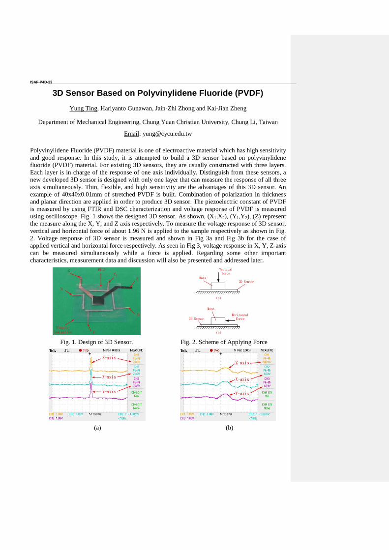
ISAF-P4D-22 ____________________________________________________________________________________________________________________
3D Sensor Based on Polyvinylidene Fluoride (PVDF)
Yung Ting, Hariyanto Gunawan, Jain-Zhi Zhong and Kai-Jian Zheng
Department of Mechanical Engineering, Chung Yuan Christian University, Chung Li, Taiwan
Email: [email protected]
Polyvinylidene Fluoride (PVDF) material is one of electroactive material which has high sensitivity
and good response. In this study, it is attempted to build a 3D sensor based on polyvinylidene
fluoride (PVDF) material. For existing 3D sensors, they are usually constructed with three layers.
Each layer is in charge of the response of one axis individually. Distinguish from these sensors, a
new developed 3D sensor is designed with only one layer that can measure the response of all three
axis simultaneously. Thin, flexible, and high sensitivity are the advantages of this 3D sensor. An
example of 40x40x0.01mm of stretched PVDF is built. Combination of polarization in thickness
and planar direction are applied in order to produce 3D sensor. The piezoelectric constant of PVDF
is measured by using FTIR and DSC characterization and voltage response of PVDF is measured
using oscilloscope. Fig. 1 shows the designed 3D sensor. As shown, (X1,X2), (Y1,Y2), (Z) represent
the measure along the X, Y, and Z axis respectively. To measure the voltage response of 3D sensor,
vertical and horizontal force of about 1.96 N is applied to the sample respectively as shown in Fig.
2. Voltage response of 3D sensor is measured and shown in Fig 3a and Fig 3b for the case of
applied vertical and horizontal force respectively. As seen in Fig 3, voltage response in X, Y, Z-axis
can be measured simultaneously while a force is applied. Regarding some other important
characteristics, measurement data and discussion will also be presented and addressed later.
Fig. 1. Design of 3D Sensor. Fig. 2. Scheme of Applying Force
(a) (b)

Fig. 3 Voltage response of 3D sensor when applying: (a) Vertical force, (b) Horizontal force
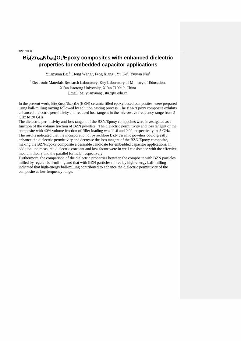
ISAF-P4D-23 ____________________________________________________________________________________________________________________
Bi2(Zn2/3Nb4/3)O7/Epoxy composites with enhanced dielectric
properties for embedded capacitor applications
Yuanyuan Bai 1
, Hong Wang1, Feng Xiang
1, Yu Ke
1, Yujuan Niu
1
1Electronic Materials Research Laboratory, Key Laboratory of Ministry of Education,
Xi’an Jiaotong University, Xi’an 710049, China
Email: [email protected]
In the present work, Bi2(Zn2/3Nb4/3)O7 (BZN) ceramic filled epoxy based composites were prepared
using ball-milling mixing followed by solution casting process. The BZN/Epoxy composite exhibits
enhanced dielectric permittivity and reduced loss tangent in the microwave frequency range from 5
GHz to 20 GHz.
The dielectric permittivity and loss tangent of the BZN/Epoxy composites were investigated as a
function of the volume fraction of BZN powders. The dielectric permittivity and loss tangent of the
composite with 40% volume fraction of filler loading was 11.6 and 0.02, respectively, at 5 GHz.
The results indicated that the incorporation of pyrochlore BZN ceramic powders could greatly
enhance the dielectric permittivity and decrease the loss tangent of the BZN/Epoxy composite,
making the BZN/Epoxy composite a desirable candidate for embedded capacitor applications. In
addition, the measured dielectric constant and loss factor were in well consistence with the effective
medium theory and the parallel formula, respectively.
Furthermore, the comparison of the dielectric properties between the composite with BZN particles
milled by regular ball-milling and that with BZN particles milled by high-energy ball-milling
indicated that high-energy ball-milling contributed to enhance the dielectric permittivity of the
composite at low frequency range.

320 340 360 380 400 420 440
0,0
0,5
1,0
1,5
2,0
2,5
3,0
0,0
5,0x10³
1,0x10⁴
1,5x10⁴
2,0x10⁴
2,5x10⁴
(
ED
C=
0)
EC (
K)
T (K)
E (kV/cm)
2
7,5
30
60
90
ISAF-P4D-24 ____________________________________________________________________________________________________________________
Electrocaloric properties of 0.7Pb(Mg1/3Nb2/3)O3–0.3PbTiO3
ceramics
Marko Vrabelj1, 2
, Hana Uršič1, 3
, Brigita Rožič1, 3
, Zdravko Kutnjak2, 4
, Silvo Drnovšek1, 3
, Barbara
Malič1, 2
1Electronic Ceramics Department, Jožef Stefan Institute, Ljubljana, Slovenia
2Jožef Stefan International Postgraduate School, Ljubljana, Slovenia
3Centre of Excellence NAMASTE, Ljubljana, Slovenia
4Condensed Matter Physics Department, Jožef Stefan Institute, Ljubljana, Slovenia
Email: [email protected]
The electrocaloric (EC) effect is a conversion of electrical energy to heat and may be defined as an
adiabatic and reversible temperature change that occurs in a polar material upon external electric
field. The aim of our work was to prepare 0.7Pb(Mg1/3Nb2/3)O3–0.3PbTiO3 (0.7PMN–0.3PT)
ceramics and to study the EC temperature change (T) vs. applied electric field and temperature.
For the synthesis of the 0.7PMN–0.3PT bulk ceramics, PbO, MgO, TiO2 and Nb2O5 were used. The
homogenized, stoichiometric powder mixtures were mechanochemically activated in a high-energy
planetary mill. The synthesized powders were milled in an attrition mill in isopropanol. The powder
compacts were sintered at 1200 °C for 2 h in a double alumina crucible in the packing powder. The
ceramics had relative density 97 % and the grain size of (1 ± 0.5) m.
In order to study EC effect by direct
approach, a high resolution calorimeter was
used. The observed magnitudes of the EC
effect confirm the existence of the large
effect in this material. A characteristic peak
of T as a function of the electric field is
observed near the critical point as shown in
Fig. 1, where T is 2.7 K at 90 kV/cm and
430 °C.377
Acknowledgments:
The contribution of Prof. Marija Kosec who passed away in December 2012 is gratefully
acknowledged. The authors would like thank Jena Cilenšek, Brigita Kmet and David Žehelj for
377
B. Rožič, M. Kosec, H. Uršič, J. Holc, B. Malič, Q. M. Zhang, R. Blinc, R. Pirc, Z. Kutnjak, Influence of the critical
point on the electrocaloric response of relaxor ferroelectrics, J. Appl. Phys., vol. 110, p. 064118 1 -5, 2011.
Fig. 123: EC temperature change T of 0.7PMN–
0.3PT ceramics as a function of temperature for
several amplitudes of the electric field. Triangles
denote the dielectric constant.1

their help with the experimental work and the Slovenian Research Agency for financial support
(research program P2-0105 and doctoral program PR-05025).
ISAF-P4D-25 ____________________________________________________________________________________________________________________
Experimental and numerical characterization of a hearing aid
prototype microphone with piezoelectric membrane
Israel Pereira1, Gustavo Martins
1, Júlio A. Cordioli
1,
1Mechanical Engineer Department, Federal University of Santa Catarina, Florianópolis, SC/Brazil
Email: [email protected]
The microphone is an important component of hearing aids. They are responsible for converting
acoustic energy into electrical energy and a proper design of this component is critical to obtain
good results in everyday life of hearing aids users. Electret microphones are the current first choice
in this kind of application but alternative designs of microphones are also been considered.
Piezoelectric microphones have numerous advantages over electrec microphones, like the reduced
number of components, very flat frequency response and high resistance to mechanical shocks.
Furthermore, piezoelectric microphones can have very simple constructions, ensuring reduced
manufacturing costs. The main difficult of using this type of microphone in hearing aids is its
typical lower sensitivity when comparing to electret ones. Many efforts are in progress to increase
the sensitivity of piezoelectric microphones and one of the most important tools to achieve that is a
proper numerical modeling of these transducers.
This paper presents the numerical modeling of a piezoelectric prototype used as a microphone. The
transducer is modeled with different variations of the Finite Element Method (FEM), including the
traditional coupled Acoustic-Structure FEM and a modified formulation that includes the effects of
viscothermal losses in the model. Also, an analysis of the load applied to the piezoelectric model is
performed in order to obtain realistic results.
The model is validated with experimental results and its sensitivity level is compared with
commercial microphones. After the validation, the numerical model can be used to optimize the
piezoelectric microphone properties in order to fulfill the requirements for hearing aids.
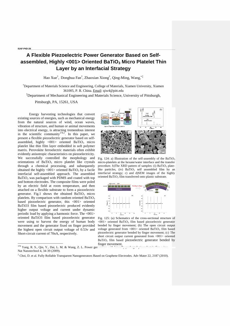
ISAF-P4D-26 ____________________________________________________________________________________________________________________
A Flexible Piezoelectric Power Generator Based on Self-
assembled, Highly <001> Oriented BaTiO3 Micro Platelet Thin
Layer by an Interfacial Strategy
Hao Xue†,
Donghua Fan
†, Zhaoxian Xiong
†, Qing-Ming, Wang,
‡
†Department of Materials Science and Engineering, College of Materials, Xiamen University, Xiamen
361005, P. R. China. Email: [email protected] ‡Department of Mechanical Engineering and Materials Science, University of Pittsburgh,
Pittsburgh, PA, 15261, USA
Energy harvesting technologies that convert
existing sources of energies, such as mechanical energy
from the natural sources of wind, ocean waves,
vibration of structure, and human or animal movements
into electrical energy, is attracting tremendous interest
in the scientific community378,2
. In this paper, we
present a flexible piezoelectric generator based on self-
assembled, highly <001> oriented BaTiO3 micro
platelet like thin film layer embedded in soft polymer
matrix. Perovskite ferroelectric materials often exhibit
evidently anisotropic characteristics on piezoelectricity.
We successfully controlled the morphology and
orientations of BaTiO3 micro platelet like crystals
through a chemical processing, and subsequently
obtained the highly <001> oriented BaTiO3 by a facile
interfacial self-assembled approach. The assembled
BaTiO3 was packaged with PDMS and coated with top
and bottom electrodes. The composite films were poled
by an electric field at room temperature, and then
attached on a flexible substrate to form a piezoelectric
generator. Fig.1 shows the obtained BaTiO3 micro
platelets. By comparison with random oriented BaTiO3
based piezoelectric generator, this <001> oriented
BaTiO3 film based piezoelectric produced evidently
higher output voltage and current under dynamic
periodic load by applying a harmonic force. The <001>
oriented BaTiO3 film based piezoelectric generator
were using to harvest the energy of human body
movement and the generator fixed on finger provided
the highest open circuit output voltage of 0.53v and
Short-circuit current of 70nA, respectively.
378
Yang, R. S., Qin, Y., Dai, L. M. & Wang, Z. L. Power generation with laterally packaged piezoelectric fine wires.
Nat Nanotechnol 4, 34-39 (2009). 2 Choi, D. et al. Fully Rollable Transparent Nanogenerators Based on Graphene Electrodes. Adv Mater 22, 2187 (2010).
Fig. 124: a) Illustration of the self-assembly of the BaTiO3
micro-platelets at the hexane/water interface and the transfer
procedure. b)The XRD pattern of samples: (i) BaTiO3 plate-
like particles, (iv) BaTiO3 self assembled film by an
interfacial strategy; c) and d)SEM images of the highly
oriented BaTiO3 film transferred onto plastic substrate.
Fig. 125: (a) Schematics of the cross-sectional structure of
<001> oriented BaTiO3 film based piezoelectric generator
bended by finger movement; (b) The open circuit output
voltage generated from <001> oriented BaTiO3 film based
piezoelectric generator bended by finger movement; (c) The
short circuit output current generated from <001> oriented
BaTiO3 film based piezoelectric generator bended by
finger movement.
ISAF-P4D-27 ____________________________________________________________________________________________________________________
Photocurrent Characteristics of PbTiO3/TiO2 Heterostructure
Nanotubes
using Anodic TiO2 Nanotubes
Sung Sik Won*, Chang Won Ahn and Ill Won Kim
Department of Physics and Energy Harvest-Storage Research Center,
University of Ulsan, Ulsan 680-749, South Korea
When electrically poled ferroelectric materials are illuminated by light beam, photo-voltage and
photo-current can be generated due to the separation of photoinduced electrons and holes by its
internal electric field. Such photovoltaic phenomena in the ferroelectric thin films exhibit potential
applications for realizing remote control and wireless energy transfer in microelectromechanical
system (MEMS) devices. In this study, we have grown TiO2 nanotube layers on sputter-deposited
Ti thin films by glycerol/NH4F electrolytes. PbTiO3/TiO2 heterostructure nanotube was obtained by
deposited Pb into the highly ordered TiO2 nanotube layers and thermally annealed in the oxygen
ambient. The crystalline structure and surface morphology of PbTiO3/TiO2 heterostructure
nanotubes were investigated by XRD and FE-SEM studies. Compared with pure TiO2 nanotube
array, the PbTiO3/TiO2 heterostructures exhibited enhanced photocurrent under UV light
irradiation.

ISAF-P4D-28 ____________________________________________________________________________________________________________________
Planar acoustic metamaterials with the active control of
acoustic impedance using a piezoelectric composite actuator
K. Nováková1, P. Mokrý
2, J. Václavík
2, P. Márton
2, M. Černík
2, P. Psota
1, R. Doleček
1, V. Lédl
1
1 Regional Centre for Special Optics and Optoelectronic Systems (TOPTEC),
Sobotecká 1660, CZ-51101 Turnov, Czech Republic 2 Institute of Mechatronics and Computer Engineering, Technical University of Liberec
Studentská 2, Liberec I, CZ-46117 Czech Republic
Email: [email protected]
Noise and vibrations affect our lives and the intensity of generated noise and vibrations has become
an important parameter indicating the quality of the environment. One of the major noise sources in
our homes and offices are vibrations of windows and glazed facades. Propagation of acoustic
energy in an acoustic medium and the reflection of noise at interfaces of two different media are
controlled by a physical property called the acoustic impedance Z. By specified tuning the acoustic
impedance of the planar structure at the interface of acoustic media one can achieve devices such as
perfectly absorbing surfaces or perfect sound shields. It is clear that realization of two
aforementioned devices usually requires such values of the acoustic impedance that are not
observed in nature. Such systems are generally called acoustic metamaterials.
In the Paper, there are presented methods for a
precise active control of the acoustic impedance
of large planar structures, e.g glass plates or
shells, by means of distributed flexible
piezoelectric composite actuators which are
connected to passive or active electronic shunt
circuits. Design of tunable acoustic metamaterials
is realized using Finite Element Method
simulations and their acoustic properties are
evaluated using acoustic transmission loss
measurements (Fig. 1). Static and dynamic
displacements of the metamerials produced by
electric voltage are measured using Digital
Holographic Interferometry. We believe that
deep understanding of presented systems should
result in future applications that improve the
quality of everyday life. This work was supported
by Czech Science Foundation Project No.:
GACR 13-10365S.
Fig. 126: Acoustic transmission loss measurement
setup. Electronically tunable acoustic metamaterial
vibrates due to the incident acoustic wave and
transmits one part of the wave to the other side.
Both acoustic pressures and vibration amplitude are
measured and the acoustic transmission loss is
computed.
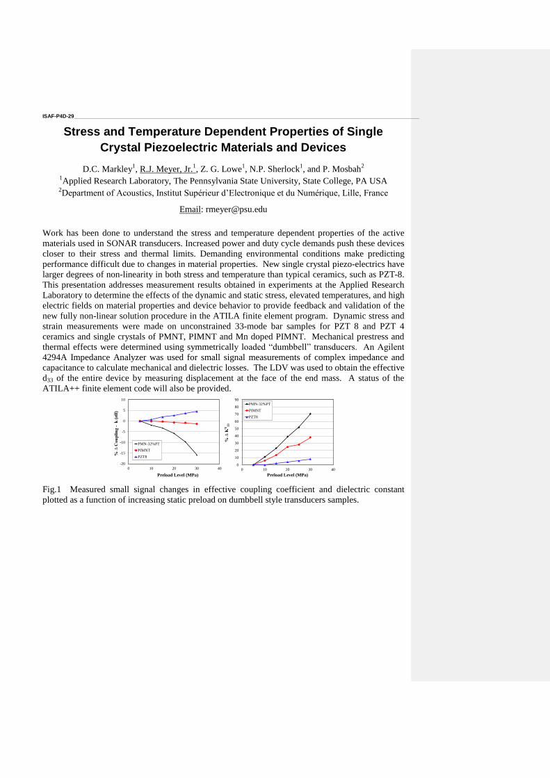
ISAF-P4D-29 ____________________________________________________________________________________________________________________
Stress and Temperature Dependent Properties of Single
Crystal Piezoelectric Materials and Devices
D.C. Markley1, R.J. Meyer, Jr.
1, Z. G. Lowe
1, N.P. Sherlock
1, and P. Mosbah
2
1Applied Research Laboratory, The Pennsylvania State University, State College, PA USA
2Department of Acoustics, Institut Supérieur d’Electronique et du Numérique, Lille, France
Email: [email protected]
Work has been done to understand the stress and temperature dependent properties of the active
materials used in SONAR transducers. Increased power and duty cycle demands push these devices
closer to their stress and thermal limits. Demanding environmental conditions make predicting
performance difficult due to changes in material properties. New single crystal piezo-electrics have
larger degrees of non-linearity in both stress and temperature than typical ceramics, such as PZT-8.
This presentation addresses measurement results obtained in experiments at the Applied Research
Laboratory to determine the effects of the dynamic and static stress, elevated temperatures, and high
electric fields on material properties and device behavior to provide feedback and validation of the
new fully non-linear solution procedure in the ATILA finite element program. Dynamic stress and
strain measurements were made on unconstrained 33-mode bar samples for PZT 8 and PZT 4
ceramics and single crystals of PMNT, PIMNT and Mn doped PIMNT. Mechanical prestress and
thermal effects were determined using symmetrically loaded “dumbbell” transducers. An Agilent
4294A Impedance Analyzer was used for small signal measurements of complex impedance and
capacitance to calculate mechanical and dielectric losses. The LDV was used to obtain the effective
d33 of the entire device by measuring displacement at the face of the end mass. A status of the
ATILA++ finite element code will also be provided.
Fig.1 Measured small signal changes in effective coupling coefficient and dielectric constant
plotted as a function of increasing static preload on dumbbell style transducers samples.
-20
-15
-10
-5
0
5
10
0 10 20 30 40
% ∆
Co
up
lin
g -
k (
eff)
Preload Level (MPa)
PMN-32%PT
PIMNT
PZT8
0
10
20
30
40
50
60
70
80
90
0 10 20 30 40
% ∆
KT
33
Preload Level (MPa)
PMN-32%PT
PIMNT
PZT8
ISAF-P4D-30 ____________________________________________________________________________________________________________________
Piezoelectric polymer multilayers on flexible substrate for
energy harvesting
Lei Zhang, Sharon Su Yin Oh, Ting Chong Wong, Chin Yaw Tan and Kui Yao
Institute of Materials Research and Engineering, A*STAR (Agency for Science, Technology and
Research), 3 Research Link, Singapore 117602
Email: [email protected]
Piezoelectric materials possess inherent functions of converting mechanical energy into electrical
energy and they are competitive candidates for harvesting mechanical energy from ambient
environments. One of major disadvantages of piezoelectric materials, particularly piezoelectric
polymers, for energy harvesting is the low current output with high voltage magnitude due to the
high impedance of piezoelectric materials. The high impedance of piezoelectric materials also
affects the energy output to a typical external load as a result of impedance mismatch. Adoption of
piezoelectric multilayer structure is an effective method to overcome this issue, particularly for
piezoelectric polymer materials, by providing reduced impedance, increased current output and
adjustable impedance for matching the external load impedance.
In this work, piezoelectric polymer multilayer structure is fabricated on flexible substrate and
operates in bending mode for energy harvesting. Analytical and numerical models are developed to
understand the effect of material parameters which are critical to the energy harvesting performance
of the piezoelectric multilayer structure on flexible substrate. The relationship among the maximum
output power of the piezoelectric multilayer on flexible substrate, the piezoelectric coefficient and
the dielectric permittivity is established. It is also found that the thickness of the internal electrodes
of piezoelectric multilayer significantly affects the electric energy generation in the bending mode.
The effect of impedance matching is clearly illustrated with comparison between a piezoelectric
multilayer and a piezoelectric single layer on the same flexible substrate for bending-mode energy
harvesting. Dramatic improvement on energy output is shown for a 22-layer P(VDF-TrFE)
multilayer structure on flexible substrate compared to that of a single-layer of the similar
configuration with the load resistance range of 25 Ω to 25 kΩ. A 10-layer P(VDF-TrFE)-based
multilayer structure is fabricated by solution coating process on flexible aluminum substrate with
multiple thin layer of internal metal electrodes prepared by physical vapor deposition method. The
experimental results of energy output is evaluated with electrical loading, which indicates that the
energy generated is adequate for many low power electronics.
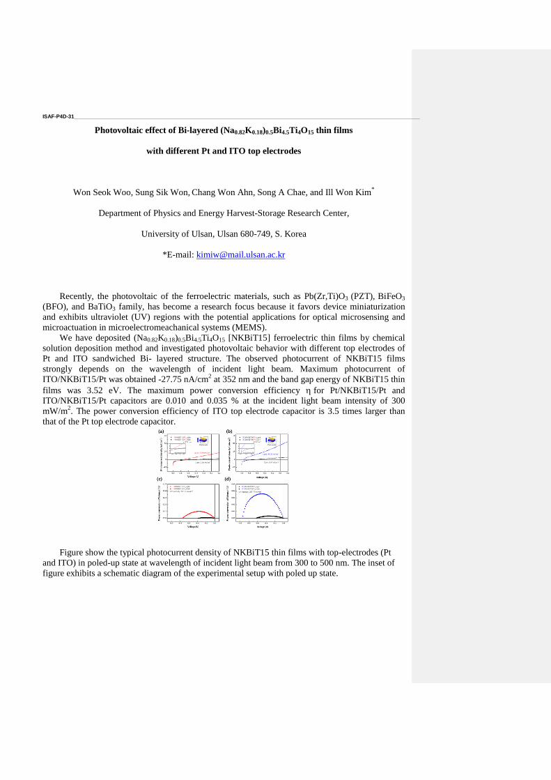
ISAF-P4D-31 ____________________________________________________________________________________________________________________
Photovoltaic effect of Bi-layered (Na0.82K0.18)0.5Bi4.5Ti4O15 thin films
with different Pt and ITO top electrodes
Won Seok Woo, Sung Sik Won, Chang Won Ahn, Song A Chae, and Ill Won Kim
*
Department of Physics and Energy Harvest-Storage Research Center,
University of Ulsan, Ulsan 680-749, S. Korea
*E-mail: [email protected]
Recently, the photovoltaic of the ferroelectric materials, such as Pb(Zr,Ti)O3 (PZT), BiFeO3
(BFO), and BaTiO3 family, has become a research focus because it favors device miniaturization
and exhibits ultraviolet (UV) regions with the potential applications for optical microsensing and
microactuation in microelectromeachanical systems (MEMS).
We have deposited (Na0.82K0.18)0.5Bi4.5Ti4O15 [NKBiT15] ferroelectric thin films by chemical
solution deposition method and investigated photovoltaic behavior with different top electrodes of
Pt and ITO sandwiched Bi- layered structure. The observed photocurrent of NKBiT15 films
strongly depends on the wavelength of incident light beam. Maximum photocurrent of
ITO/NKBiT15/Pt was obtained -27.75 nA/cm2 at 352 nm and the band gap energy of NKBiT15 thin
films was 3.52 eV. The maximum power conversion efficiency for Pt/NKBiT15/Pt and
ITO/NKBiT15/Pt capacitors are 0.010 and 0.035 % at the incident light beam intensity of 300
mW/m2. The power conversion efficiency of ITO top electrode capacitor is 3.5 times larger than
that of the Pt top electrode capacitor.
Figure show the typical photocurrent density of NKBiT15 thin films with top-electrodes (Pt
and ITO) in poled-up state at wavelength of incident light beam from 300 to 500 nm. The inset of
figure exhibits a schematic diagram of the experimental setup with poled up state.
ISAF-P4D-32 ____________________________________________________________________________________________________________________
Lead free piezoelectric AD layer for micro actuator
Jun Akedo*, Jae-Hyuk Park, and Muneyasu Suzuki
National Institute of Advanced Industrial Science and Technology (AIST) 1-2-1 Namiki, Tsukuba
305-8564 Japan
High performance micro optical scanner with wide scanning angle, high speed scanning
and large mirror size is strongly demanded for laser projection system and human detective
sensor, which are expected huge market as piezoelectric actuator in the world. We
demonstrate the lamb wave resonant optical scanning devices actuated by piezoelectric AD
film and report their temperature properties and durability. Metal-based structure was
introduced to reduce the production cost and to improve the optical scanning performance,
simultaneously. The optical scanner with large mirror size of 1~5 mm square as well as
high scanning angle of over 90 degree were fabricated. A high optical scanning angle (over
60 ˚) and high resonant frequency (over 30kHz) were achieved in ambient air without
vacuum packaging. The resonant frequency and scanning angle of scanner were not change
during life test for over 50,000 hours. In this report, BTO thick film as a lead free
piezoelectric material was prepared by aerosol deposition (AD) method for fabrication of
scanner devices. Piezoelectric d31 of BTO-AD film was approximately -138 pm/V. Also,
the performance of optical scanner driven by AD-BTO thick film was compared with that
by BTO bulk material and AD-PZT thick film. As the results, AD-BTO film can be used to
practical applications.
ISAF-P4D-33 ____________________________________________________________________________________________________________________
BiFeO3 Thin Films for Photocatalytic Water Splitting
Wei Ji1,2
, Kui Yao1*
, Yee Fun Lim1 and Yung C. Liang
2
1Institute of Materials Research and Engineering (IMRE), A*STAR (Agency for Science,
Technology and Research), 3 Research Link, Singapore 117602 2Department of Electrical and Computer Engineering, National University of Singapore, Kent
Ridge, Singapore 119260
*Email: [email protected]
Photoelectrolysis of water into hydrogen and oxygen is an attractive way to harvest the solar
energy. It converts the solar energy into chemical energy, which is much easier to store than
electricity. Semiconductor metal oxides have been widely used as photoanodes in photoelectrolytic
cells due to their electrochemical stability. An ideal photoelectrolytic cell should be able to drive
both the hydrogen and the oxygen evolutions without any external bias. However, the conduction
bands in most of the oxides studied so far are too positive to drive the hydrogen evolution. Many of
them also have a wide bandgap larger than 3 eV. Consequently, they are not able to absorb the
visible region of the solar spectrum. New suitable materials are desired to achieve unassisted water
splitting.
Ferroelectric BiFeO3 (BFO) has a direct bandgap of about 2.7 eV. Previous studies have
demonstrated its catalytic effects for water splitting under visible light379
. However, the ferroelectric
properties of BFO have not been explored in all these earlier reports. As has been shown in our
earlier works, ferroelectric polarizations can significantly affect the photovoltaic (PV) process in
epitaxial BFO thin films. The photocurrent direction can be switched by poling the BFO films in
different directions380
. This suggests that the ferroelectric polarization can be used to enhance the
catalytic properties. In this work, we studied the photoelectrolytic water splitting reaction in high
quality epitaxial BFO films. Significant anodic current is observed. The onset of the anodic
photocurrent is at 0.210 V for the 223-nm-thick films. This is shifted to -0.036 VAg/AgCl in the 112-
nm-thick films. The thinner films minimize Ohmic losses and lead to the cathodic shift of the
photocurrent onset. Furthermore, XPS measurements show that the band edges of BFO straddle the
water redox levels. By considering both the energy band positions and the ferroelectric properties,
we propose that BFO can potentially be used to achieve unassisted water splitting in a monolithic
cell.
379
F. Gao, et. al., "Visible-light photocatalytic properties of weak magnetic BiFeO3 nanoparticls", Adv. Mater., vol. 19,
p. 2889-2892, 2007. J. Deng, et. al., “Bismuth iron oxide nanoparticles as photocatalyst for solar hydrogen generation
from water”, J. Fund. Renew. Energ., vol. 1, p. 1-10, 2011. 380
W. Ji, et. al., “Bulk photovoltaic effect at visible wavelength in epitaxial ferroelectric BiFeO3 thin films”, Adv.
Mater., vol. 22, p. 1763-1766, 2010.
ISAF-P4D-34 ____________________________________________________________________________________________________________________
Actuator for precision positioning based on single crystalline
lithium niobate
Ilya Kubasov1, Mikhail Malinkovich
1, Aleksander Bykov
1, Sedrak Grigoryan
1
1National University of Science and Technology "MISiS", Moscow, Russian Federation
Email: [email protected]
Bimorphs are widely used in actuators designed for precise positioning. Usually they are made of
lead zirconate-titanate (Pb(ZrxTi1-x,)O3, PZT) piezoelectric ceramics because of its high
piezoelectric coefficients values and high electromechanical conversion coefficient. At the same
time PZT ceramics have low Curie temperature, high hysteresis, considerable temperature
dependence of the piezoelectric modules, and creep. This disadvantages limit usage of the PZT
made bimorphs and also make additional scanners calibration necessary.
In our previous work the ability to use single crystalline lithium niobate (LN) in the devices for
precise displacement has been considered381
. To realize bimorph structure it’s necessary to form
two domains with the opposite orientation of spontaneous polarization vector in a crystal plate. The
bimorph based on LN single crystal has stability in wide temperature range due to Tc about 1200
°C, the absence of hysteresis and creep.
In this study bimorphs were made of single crystal LN plates by using non-uniform thermal field.
Magnetron sputtering was used to make gold electrodes on the bimorph surface. Cantilevered
bending displacements of the 6 cm LN bimorph were ≈±20 μm in the voltage within ±300 V. Single
crystal LN bimorph actuators can be used for exact positioning in probe microscope techniques, for
laser resonators adjustment and as wave guides with exact variable geometrical characteristics.
381
Antipov V.V., Bykov A.S., Malinkovich M.D., Parkhomenko Y.N., “Formation of bidomain structure in lithium
niobate single crystals by electrothermal method”, Ferroelectrics, vol. 374, p. 701–708, 2008.
ISAF-P4D-35 ____________________________________________________________________________________________________________________
NUMERICAL SIMULATION ANALYSIS FOR A NOVEL SHAPES OF PIEZOLECTRIC COUPLED WITH TUBE TO INCREASE THE
RADIAL DISPLACEMENT Yung Ting, Tzung-Shiuan Tsai, Amelia Sugondo and Yen-Lung Lee
Department of Mechanical Engineering, Chung Yuan Christian University, 200, Chung Pei Rd. Chung Li, Taiwan 32023, ROC
Email:[email protected]
In this paper, piezoelectric actuators that constructed with a ring or several equal sectional type of piezoelectric
ceramics attached to a thin tube are designed. The generated amplitude in the radial vibration of tube and other
characteristics is investigated. Finite element method (FEM) is used to analyze the mode shape, resonance frequency and
amplitude. The analytical and experimental results show a good agreement. From the results, there is no significant difference
of the resonance frequency between the ring-type and sectional-type ceramic actuators. However, the sectional-type one is
able to generate more radial amplitude. In particular, the sectional-type ceramic actuator with arc 60o and with equal
clearance between the neighboring actuators performs the best.
Key words: piezoelectric tube, piece-by-piece piezoelectric, radially polarization, amplitude
Design of Piezoelectric Actuator
A. Resonance Frequency For a general tube structure, resonance frequency
can be calculated by fr= C/2L where fr is the
resonance frequency, L is the length of the device,
and C is the speed of sound. It indicates longer length
of the structure would reduce the resonance
frequency.
B. Vibration Amplitude
Piezoelectric actuator is mounted on the tube as
illustrated in Figure 1. Two types of piezoelectric
actuators, ring and sectional, are depicted in Figure 2.
A ring type piezoelectric actuator encircled the tube
with no clearance is shown in Figure 2(a), named
TYPE I. Two cases, with arc 120o and 60
o of each
section of piezoelectric actuator with equivalent
clearance in between the actuators for the sectional
type are illustrated in Figure 2(b) and 2(c), named
TYPE II and TYPE III respectively. All the ring and
sectional types of piezoelectric actuators are made of
PZT-5A higher piezoelectric coefficient d31 and d33 in
comparison with PZT-4 at room temperature. The
tube is made of stainless steel because of high tensile
strength as well as elastic limit that is suitable for
high power ultrasound design.
Simulation and Experiment Result
Note that, mode shape of tube with half wavelength is
the design purpose. Using ANSYS, an example of
appropriate mode shape is found and deformation
with applied voltage of 50V is shown in Figure 3. As
expected, resonance frequency decreases when the
length of the tube increases. Also, resonance
frequency is inversely proportional to the length of
the rube. The first mode of simple axisymmetric
deformation generating half wave is chosen to
determine the resonance frequency by the modal
analysis. Harmonic analysis is used to examine the
vibration amplitude at the chosen resonance
frequency. Figure 4 shows the harmonic simulation
and experiment results employed with, for example
50V and 150V. The simulation results show that
amplitude of radial vibration of the tube is very small
for the ring type (TYPE I) but quite large for the
sectional type. Compared to the amplitude of TYPE I,
TYPE II is about one thousand times, and TYPE III is
about twenty thousand times. As seen, amplitude of
TYPE I presents with very small difference as tube
length is changed, and amplitude of TYPE II is
varying, and, amplitude of TYPE III is increased for
longer tube but there is a maximum value for the
length of about 47.5mm.

Fig. 1 Tube encircled with piezoelectric actuator
60∘
120∘
60∘
60∘
Fig. 2. Type and structure implementation of piezoelectric Fig. 3. Amplitude for the Fig. 4. Amplitude vs. Length
actuator: (a) Ring-type piezoelectric actuator encircles length of tube 50 mm for Ring and Sectional type
the tube, (b) Sectional-type (120o) piezoelectric actuator,
(c) Sectional-type (60o) piezoelectric actuator
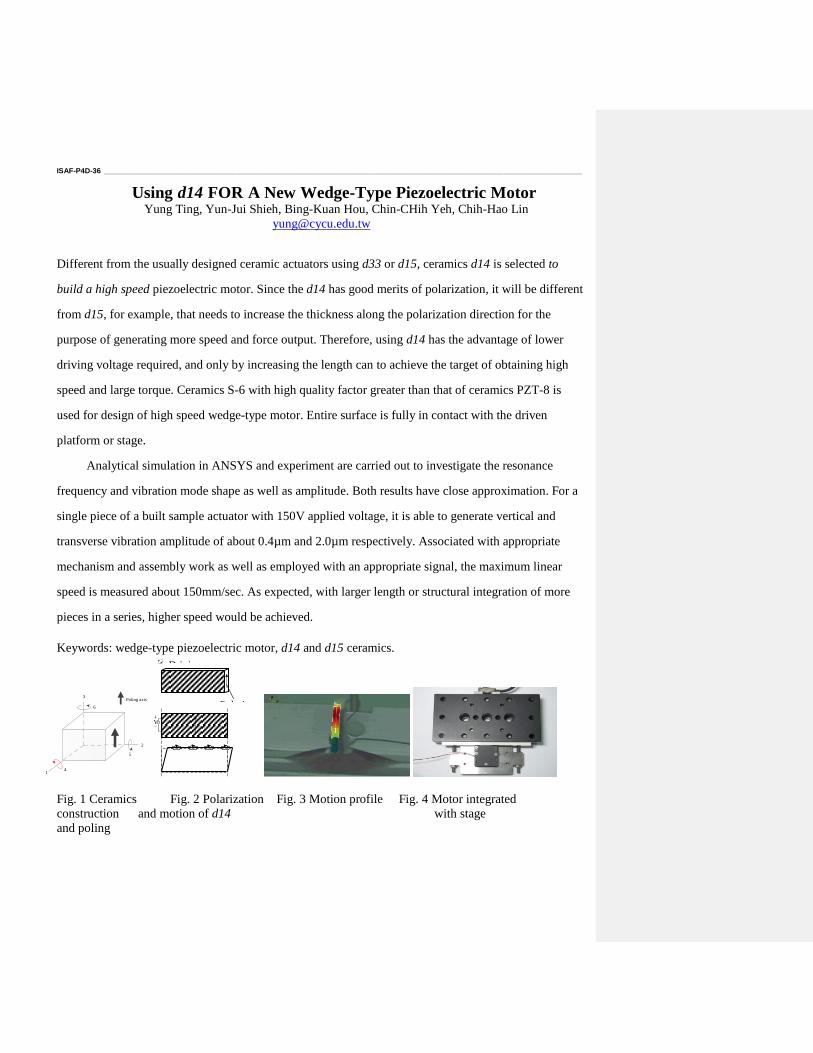
ISAF-P4D-36 ___________________________________________________________________________________________________________________
Using d14 FOR A New Wedge-Type Piezoelectric Motor Yung Ting, Yun-Jui Shieh, Bing-Kuan Hou, Chin-CHih Yeh, Chih-Hao Lin
Different from the usually designed ceramic actuators using d33 or d15, ceramics d14 is selected to
build a high speed piezoelectric motor. Since the d14 has good merits of polarization, it will be different
from d15, for example, that needs to increase the thickness along the polarization direction for the
purpose of generating more speed and force output. Therefore, using d14 has the advantage of lower
driving voltage required, and only by increasing the length can to achieve the target of obtaining high
speed and large torque. Ceramics S-6 with high quality factor greater than that of ceramics PZT-8 is
used for design of high speed wedge-type motor. Entire surface is fully in contact with the driven
platform or stage.
Analytical simulation in ANSYS and experiment are carried out to investigate the resonance
frequency and vibration mode shape as well as amplitude. Both results have close approximation. For a
single piece of a built sample actuator with 150V applied voltage, it is able to generate vertical and
transverse vibration amplitude of about 0.4µm and 2.0µm respectively. Associated with appropriate
mechanism and assembly work as well as employed with an appropriate signal, the maximum linear
speed is measured about 150mm/sec. As expected, with larger length or structural integration of more
pieces in a series, higher speed would be achieved.
Keywords: wedge-type piezoelectric motor, d14 and d15 ceramics.
1
3
2
4
5
6
Poling axis
Fig. 1 Ceramics Fig. 2 Polarization Fig. 3 Motion profile Fig. 4 Motor integrated
construction and motion of d14 with stage
and poling
V
Drivin
g
Electro
de Polariz
ation
directio
n
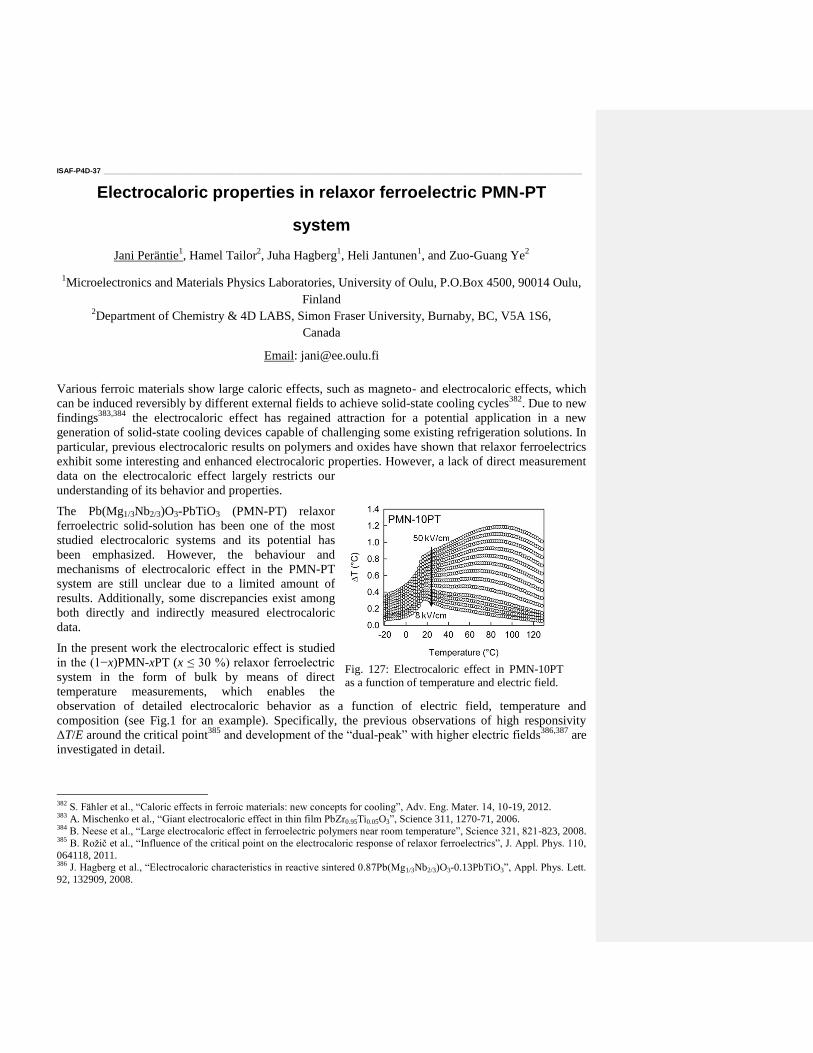
ISAF-P4D-37 ___________________________________________________________________________________________________________________
Electrocaloric properties in relaxor ferroelectric PMN-PT
system
Jani Peräntie1, Hamel Tailor
2, Juha Hagberg
1, Heli Jantunen
1, and Zuo-Guang Ye
2
1Microelectronics and Materials Physics Laboratories, University of Oulu, P.O.Box 4500, 90014 Oulu,
Finland 2Department of Chemistry & 4D LABS, Simon Fraser University, Burnaby, BC, V5A 1S6,
Canada
Email: [email protected]
Various ferroic materials show large caloric effects, such as magneto- and electrocaloric effects, which
can be induced reversibly by different external fields to achieve solid-state cooling cycles382
. Due to new
findings383,384
the electrocaloric effect has regained attraction for a potential application in a new
generation of solid-state cooling devices capable of challenging some existing refrigeration solutions. In
particular, previous electrocaloric results on polymers and oxides have shown that relaxor ferroelectrics
exhibit some interesting and enhanced electrocaloric properties. However, a lack of direct measurement
data on the electrocaloric effect largely restricts our
understanding of its behavior and properties.
The Pb(Mg1/3Nb2/3)O3-PbTiO3 (PMN-PT) relaxor
ferroelectric solid-solution has been one of the most
studied electrocaloric systems and its potential has
been emphasized. However, the behaviour and
mechanisms of electrocaloric effect in the PMN-PT
system are still unclear due to a limited amount of
results. Additionally, some discrepancies exist among
both directly and indirectly measured electrocaloric
data.
In the present work the electrocaloric effect is studied
in the (1−x)PMN-xPT (x ≤ 30 %) relaxor ferroelectric
system in the form of bulk by means of direct
temperature measurements, which enables the
observation of detailed electrocaloric behavior as a function of electric field, temperature and
composition (see Fig.1 for an example). Specifically, the previous observations of high responsivity
ΔT/E around the critical point385
and development of the “dual-peak” with higher electric fields386,387
are
investigated in detail.
382
S. Fähler et al., “Caloric effects in ferroic materials: new concepts for cooling”, Adv. Eng. Mater. 14, 10-19, 2012. 383
A. Mischenko et al., “Giant electrocaloric effect in thin film PbZr0.95Ti0.05O3”, Science 311, 1270-71, 2006. 384
B. Neese et al., “Large electrocaloric effect in ferroelectric polymers near room temperature”, Science 321, 821-823, 2008. 385
B. Rožič et al., “Influence of the critical point on the electrocaloric response of relaxor ferroelectrics”, J. Appl. Phys. 110,
064118, 2011. 386
J. Hagberg et al., “Electrocaloric characteristics in reactive sintered 0.87Pb(Mg1/3Nb2/3)O3-0.13PbTiO3”, Appl. Phys. Lett.
92, 132909, 2008.
Fig. 127: Electrocaloric effect in PMN-10PT
as a function of temperature and electric field.
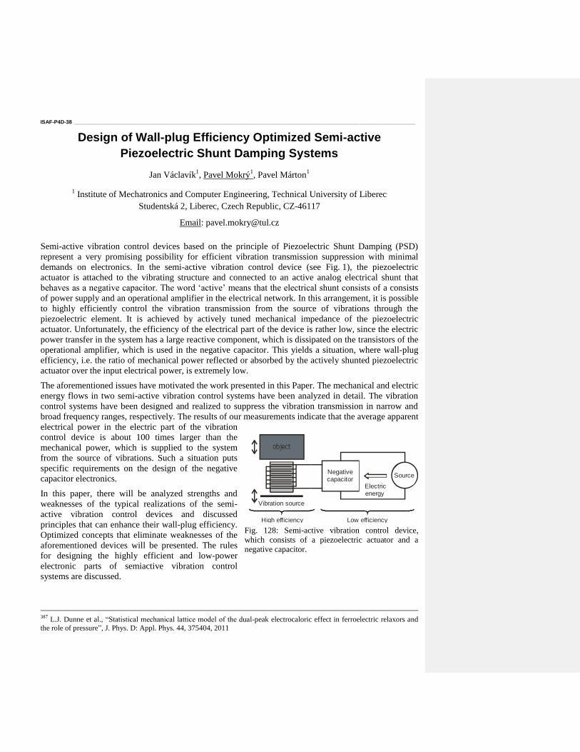
ISAF-P4D-38 ___________________________________________________________________________________________________________________
Design of Wall-plug Efficiency Optimized Semi-active
Piezoelectric Shunt Damping Systems
Jan Václavík1, Pavel Mokrý
1, Pavel Márton
1
1 Institute of Mechatronics and Computer Engineering, Technical University of Liberec
Studentská 2, Liberec, Czech Republic, CZ-46117
Email: [email protected]
Semi-active vibration control devices based on the principle of Piezoelectric Shunt Damping (PSD)
represent a very promising possibility for efficient vibration transmission suppression with minimal
demands on electronics. In the semi-active vibration control device (see Fig. 1), the piezoelectric
actuator is attached to the vibrating structure and connected to an active analog electrical shunt that
behaves as a negative capacitor. The word ‘active’ means that the electrical shunt consists of a consists
of power supply and an operational amplifier in the electrical network. In this arrangement, it is possible
to highly efficiently control the vibration transmission from the source of vibrations through the
piezoelectric element. It is achieved by actively tuned mechanical impedance of the piezoelectric
actuator. Unfortunately, the efficiency of the electrical part of the device is rather low, since the electric
power transfer in the system has a large reactive component, which is dissipated on the transistors of the
operational amplifier, which is used in the negative capacitor. This yields a situation, where wall-plug
efficiency, i.e. the ratio of mechanical power reflected or absorbed by the actively shunted piezoelectric
actuator over the input electrical power, is extremely low.
The aforementioned issues have motivated the work presented in this Paper. The mechanical and electric
energy flows in two semi-active vibration control systems have been analyzed in detail. The vibration
control systems have been designed and realized to suppress the vibration transmission in narrow and
broad frequency ranges, respectively. The results of our measurements indicate that the average apparent
electrical power in the electric part of the vibration
control device is about 100 times larger than the
mechanical power, which is supplied to the system
from the source of vibrations. Such a situation puts
specific requirements on the design of the negative
capacitor electronics.
In this paper, there will be analyzed strengths and
weaknesses of the typical realizations of the semi-
active vibration control devices and discussed
principles that can enhance their wall-plug efficiency.
Optimized concepts that eliminate weaknesses of the
aforementioned devices will be presented. The rules
for designing the highly efficient and low-power
electronic parts of semiactive vibration control
systems are discussed.
387
L.J. Dunne et al., “Statistical mechanical lattice model of the dual-peak electrocaloric effect in ferroelectric relaxors and
the role of pressure”, J. Phys. D: Appl. Phys. 44, 375404, 2011
Vibration source
High efficiency Low efficiency
Negativecapacitor
Source
Electricenergy
Fig. 128: Semi-active vibration control device,
which consists of a piezoelectric actuator and a
negative capacitor.

ISAF-P4D-39 ___________________________________________________________________________________________________________________
Efficiency measurement in piezoelectric vibration energy
harvesters.
P. M. Weaver1, P. Woolliams
1, M.G. Cain
1, M. Stewart
1
1National Physical Laboratory, Teddington, UK
Email: [email protected]
Vibrational energy harvesters convert energy from vibrations and movement in the environment into
electrical energy which can be used to power a device such as a wireless sensor node. The energy source
is often considered as “waste” energy and energy harvesting performance is typically characterised by
power output under specified conditions of vibration amplitude and frequency. This takes no account of
the energy extracted from or available from the source. This is important where account needs to be
taken of the loading of the source by the harvester. This includes “parasitic” harvesting where the energy
derived from the source is not “free” or wasted, and use of the energy harvester increases the power
consumed by the source. Examples include human or vehicle powered applications where it is the
availability of the energy source rather than energy saving that is the main motivation. It is also
important in situations where the power from the source is limited. In these cases, the ratio of power out
to power in, or the efficiency needs to be known.
Measuring efficiency is more complex than measuring power out under well-defined vibration
conditions, because of the requirement to measure the power transferred from the source to the energy
harvester. Often the harvested power is a small fraction of the total power delivered by the system. We
are not aware of any published reports of measurement of efficiency, although it is discussed in some
mathematical models of energy harvesters.
In this paper we describe an experimental method of measuring efficiency for resonant piezoelectric
cantilever energy harvesters based on a damped oscillator response to an impulse input. Experimental
results for typical energy harvesting devices are presented.
This work has been performed in the framework of the joint research project “Metrology for Energy
Harvesting”, which is supported by the European Metrology Research Programme (EMRP), jointly
funded by the EMRP participating countries within EURAMET and the European Union.
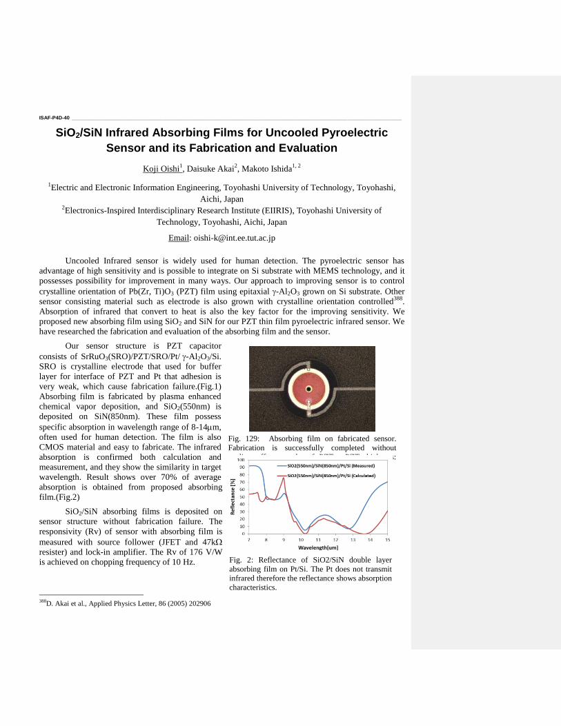
ISAF-P4D-40 ___________________________________________________________________________________________________________________
SiO2/SiN Infrared Absorbing Films for Uncooled Pyroelectric
Sensor and its Fabrication and Evaluation
Koji Oishi1, Daisuke Akai
2, Makoto Ishida
1, 2
1Electric and Electronic Information Engineering, Toyohashi University of Technology, Toyohashi,
Aichi, Japan 2Electronics-Inspired Interdisciplinary Research Institute (EIIRIS), Toyohashi University of
Technology, Toyohashi, Aichi, Japan
Email: [email protected]
Uncooled Infrared sensor is widely used for human detection. The pyroelectric sensor has
advantage of high sensitivity and is possible to integrate on Si substrate with MEMS technology, and it
possesses possibility for improvement in many ways. Our approach to improving sensor is to control
crystalline orientation of Pb(Zr, Ti)O3 (PZT) film using epitaxial -Al2O3 grown on Si substrate. Other
sensor consisting material such as electrode is also grown with crystalline orientation controlled388
.
Absorption of infrared that convert to heat is also the key factor for the improving sensitivity. We
proposed new absorbing film using SiO2 and SiN for our PZT thin film pyroelectric infrared sensor. We
have researched the fabrication and evaluation of the absorbing film and the sensor.
Our sensor structure is PZT capacitor
consists of SrRuO3(SRO)/PZT/SRO/Pt/-Al2O3/Si.
SRO is crystalline electrode that used for buffer
layer for interface of PZT and Pt that adhesion is
very weak, which cause fabrication failure.(Fig.1)
Absorbing film is fabricated by plasma enhanced
chemical vapor deposition, and SiO2(550nm) is
deposited on SiN(850nm). These film possess
specific absorption in wavelength range of 8-14m,
often used for human detection. The film is also
CMOS material and easy to fabricate. The infrared
absorption is confirmed both calculation and
measurement, and they show the similarity in target
wavelength. Result shows over 70% of average
absorption is obtained from proposed absorbing
film.(Fig.2)
SiO2/SiN absorbing films is deposited on
sensor structure without fabrication failure. The
responsivity (Rv) of sensor with absorbing film is
measured with source follower (JFET and 47k
resister) and lock-in amplifier. The Rv of 176 V/W
is achieved on chopping frequency of 10 Hz.
388
D. Akai et al., Applied Physics Letter, 86 (2005) 202906
Fig. 129: Absorbing film on fabricated sensor.
Fabrication is successfully completed without
peeling off or cracks of PZT. PZT thickness:
450nm
Fig. 2: Reflectance of SiO2/SiN double layer
absorbing film on Pt/Si. The Pt does not transmit
infrared therefore the reflectance shows absorption
characteristics.
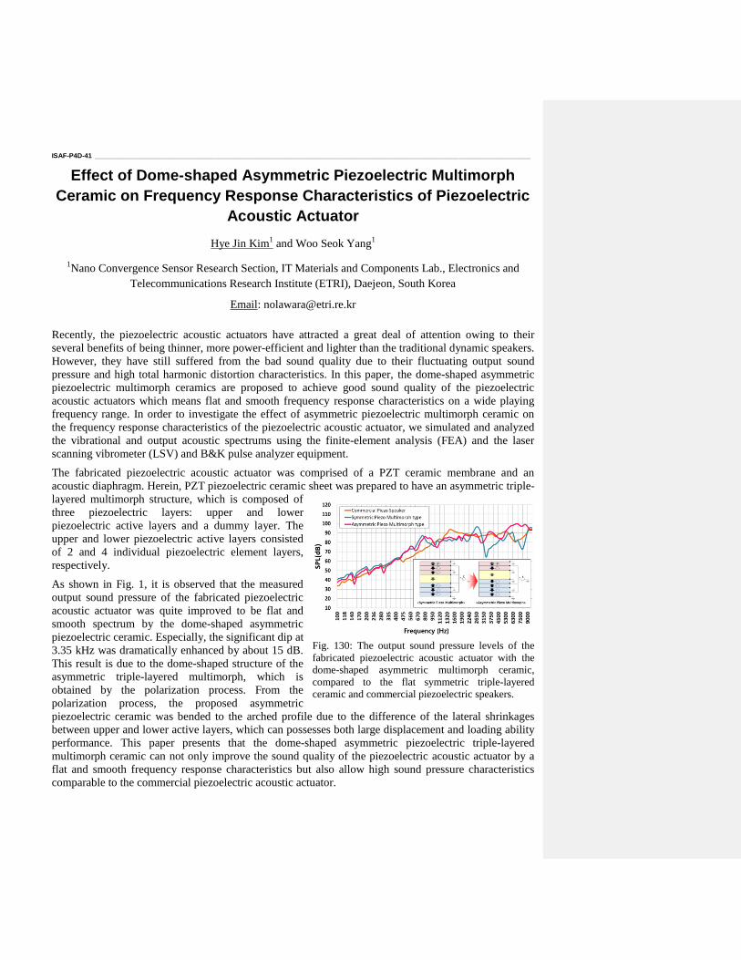
ISAF-P4D-41 ___________________________________________________________________________________________________________________
Effect of Dome-shaped Asymmetric Piezoelectric Multimorph
Ceramic on Frequency Response Characteristics of Piezoelectric
Acoustic Actuator
Hye Jin Kim1 and Woo Seok Yang
1
1Nano Convergence Sensor Research Section, IT Materials and Components Lab., Electronics and
Telecommunications Research Institute (ETRI), Daejeon, South Korea
Email: [email protected]
Recently, the piezoelectric acoustic actuators have attracted a great deal of attention owing to their
several benefits of being thinner, more power-efficient and lighter than the traditional dynamic speakers.
However, they have still suffered from the bad sound quality due to their fluctuating output sound
pressure and high total harmonic distortion characteristics. In this paper, the dome-shaped asymmetric
piezoelectric multimorph ceramics are proposed to achieve good sound quality of the piezoelectric
acoustic actuators which means flat and smooth frequency response characteristics on a wide playing
frequency range. In order to investigate the effect of asymmetric piezoelectric multimorph ceramic on
the frequency response characteristics of the piezoelectric acoustic actuator, we simulated and analyzed
the vibrational and output acoustic spectrums using the finite-element analysis (FEA) and the laser
scanning vibrometer (LSV) and B&K pulse analyzer equipment.
The fabricated piezoelectric acoustic actuator was comprised of a PZT ceramic membrane and an
acoustic diaphragm. Herein, PZT piezoelectric ceramic sheet was prepared to have an asymmetric triple-
layered multimorph structure, which is composed of
three piezoelectric layers: upper and lower
piezoelectric active layers and a dummy layer. The
upper and lower piezoelectric active layers consisted
of 2 and 4 individual piezoelectric element layers,
respectively.
As shown in Fig. 1, it is observed that the measured
output sound pressure of the fabricated piezoelectric
acoustic actuator was quite improved to be flat and
smooth spectrum by the dome-shaped asymmetric
piezoelectric ceramic. Especially, the significant dip at
3.35 kHz was dramatically enhanced by about 15 dB.
This result is due to the dome-shaped structure of the
asymmetric triple-layered multimorph, which is
obtained by the polarization process. From the
polarization process, the proposed asymmetric
piezoelectric ceramic was bended to the arched profile due to the difference of the lateral shrinkages
between upper and lower active layers, which can possesses both large displacement and loading ability
performance. This paper presents that the dome-shaped asymmetric piezoelectric triple-layered
multimorph ceramic can not only improve the sound quality of the piezoelectric acoustic actuator by a
flat and smooth frequency response characteristics but also allow high sound pressure characteristics
comparable to the commercial piezoelectric acoustic actuator.
Fig. 130: The output sound pressure levels of the
fabricated piezoelectric acoustic actuator with the
dome-shaped asymmetric multimorph ceramic,
compared to the flat symmetric triple-layered
ceramic and commercial piezoelectric speakers.
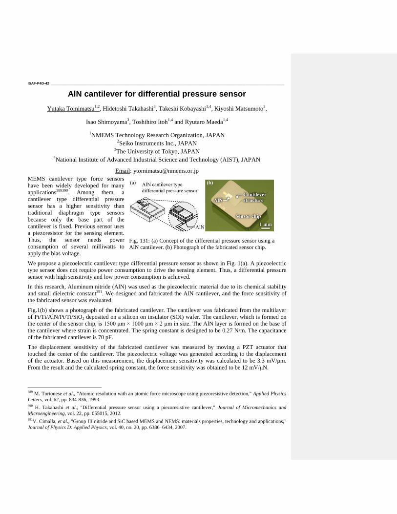
ISAF-P4D-42 ___________________________________________________________________________________________________________________
AlN cantilever for differential pressure sensor
Yutaka Tomimatsu1,2
, Hidetoshi Takahashi3, Takeshi Kobayashi
1,4, Kiyoshi Matsumoto
3,
Isao Shimoyama3, Toshihiro Itoh
1,4 and Ryutaro Maeda
1,4
1NMEMS Technology Research Organization, JAPAN
2Seiko Instruments Inc., JAPAN
3The University of Tokyo, JAPAN
4National Institute of Advanced Industrial Science and Technology (AIST), JAPAN
Email: [email protected]
MEMS cantilever type force sensors
have been widely developed for many
applications389390. Among them, a
cantilever type differential pressure
sensor has a higher sensitivity than
traditional diaphragm type sensors
because only the base part of the
cantilever is fixed. Previous sensor uses
a piezoresistor for the sensing element.
Thus, the sensor needs power
consumption of several milliwatts to
apply the bias voltage.
We propose a piezoelectric cantilever type differential pressure sensor as shown in Fig. 1(a). A piezoelectric
type sensor does not require power consumption to drive the sensing element. Thus, a differential pressure
sensor with high sensitivity and low power consumption is achieved.
In this research, Aluminum nitride (AlN) was used as the piezoelectric material due to its chemical stability
and small dielectric constant391. We designed and fabricated the AlN cantilever, and the force sensitivity of
the fabricated sensor was evaluated.
Fig.1(b) shows a photograph of the fabricated cantilever. The cantilever was fabricated from the multilayer
of Pt/Ti/AlN/Pt/Ti/SiO2 deposited on a silicon on insulator (SOI) wafer. The cantilever, which is formed on
the center of the sensor chip, is 1500 μm × 1000 μm × 2 μm in size. The AlN layer is formed on the base of
the cantilever where strain is concentrated. The spring constant is designed to be 0.27 N/m. The capacitance
of the fabricated cantilever is 70 pF.
The displacement sensitivity of the fabricated cantilever was measured by moving a PZT actuator that
touched the center of the cantilever. The piezoelectric voltage was generated according to the displacement
of the actuator. Based on this measurement, the displacement sensitivity was calculated to be 3.3 mV/μm.
From the result and the calculated spring constant, the force sensitivity was obtained to be 12 mV/μN.
389
M. Tortonese et al., "Atomic resolution with an atomic force microscope using piezoresistive detection," Applied Physics
Letters, vol. 62, pp. 834-836, 1993. 390
H. Takahashi et al., "Differential pressure sensor using a piezoresistive cantilever," Journal of Micromechanics and
Microengineering, vol. 22, pp. 055015, 2012. 391
V. Cimalla, et al., "Group III nitride and SiC based MEMS and NEMS: materials properties, technology and applications,"
Journal of Physics D: Applied Physics, vol. 40, no. 20, pp. 6386–6434, 2007.
Fig. 131: (a) Concept of the differential pressure sensor using a
AlN cantilever. (b) Photograph of the fabricated sensor chip.
ISAF-P4D-43 ___________________________________________________________________________________________________________________
Application driven design, fabrication and characterization of
piezoelectric energy scavenger for cardiac pacemakers
Mikael Colin, Libor Rufer, Skandar Basrour
TIMA (CNRS, G-INP, UJF), Grenoble, FRANCE
Email: [email protected]
The disruptive innovation in pacemakers and implantable cardioverter defibrillators (ICDs) will provide
implants that do not require electrical leads. Main actors in the field of cardiac rhythm management
(CRM) implants prepare miniaturized and autonomous leadless implants, which could be directly placed
inside a human heart. Several concepts for powering stand-alone cardiac implants were proposed392
in
the past, and recently the first study of an energy scavenging system placed in the human heart has been
presented393
. The study was conducted for a relatively large system operating at 40 Hz. We will
demonstrate, that according to the heart beat acceleration spectrum obtained by placing accelerometers
inside several heart cavities394
, the useful vibration energy is rather localized at lower frequencies (15 to
30 Hz). We will also detail the dimensional restrictions in the case of a leadless pacemaker. Since it has
to be placed into a heart through veins, the device is expected to be of cylindrical shape with a diameter
of about 6 mm.
We will present the design, simulation, fabrication and characterization of piezoelectric vibration energy
scavenger for cardiac implants. We will discuss the energy content of the heart vibration spectrum in a
view of energy harvesting. We will place emphasis on the nature of the spectrum, the energy frequencies
and corresponding amplitudes. We will present an application driven design of a resonant piezoelectric
energy scavenger aiming at powering a leadless pacemaker with a useable energy of few µJ per
heartbeat. Such an energy scavenger consists of a piezoelectric bimorph cantilever with 20 µm thick
Pb(ZrxTi1-x)O3 layers. A simulation study in both ANSYS® and Simulink® environments, has shown
that the proposed design delivers the required energy.
However, none of the current fabrication processes can be used for manufacturing such PZT thick films.
Using processes derived from the microelectronic field such as Sol Gel deposition or sputtering, the
maximum achievable thickness is about 2 to 5 µm. In contrary, using co-firing techniques, the PZT
plates can hardly be thinner than 100 µm. As a
consequence, the manufacturing of the above-described
piezoelectric scavenger corresponds to an actual process blind
window. In this paper, we present the fabrication of an ultra
low-frequency device (15 Hz) using optimized grinding and
polishing techniques. The obtained experimental results are in
good agreement with our analytical and numerical
modeling (Figure 1).
392
W. H. Ko, “Piezoelectric energy converter for electronic implants”, US patent 3,456,134, 1969. 393
M. A. Karami, D. J. Inman, “Powering Pacemakers from heartbeat vibration using linear and non linear energy harvester”,
Applied Physics Letters, vol. 100, 042901, 2012. 394
M. Deterre, B. Bouteaud, R. DalMolin, S. Boisseau, J-J. Chaillout, E. Lefeuvre, E. Dufour-Gergam, “Energy harvesting
system for cardiac implant applications”, Symposium on the Design, Test, Integration and Packaging of MEMS/MOEMS
(DTIP), May 11-13, 2011, pp. 387-391.
Fig.1: Experiment/simulation results
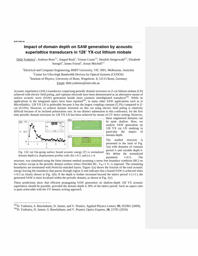
ISAF-P4D-44 ___________________________________________________________________________________________________________________
Impact of domain depth on SAW generation by acoustic
superlattice transducers in 128˚ YX-cut lithium niobate
Didit Yudistira1, Andreas Boes
1,2, Amgad Rezk
1, Tristan Crasto
1,2, Hendrik Steigerwald
1,2, Elisabeth
Soergel3, James Friend
1, Arnan Mitchell
1,2
1Electrical and Computer Engineering, RMIT University, VIC 3001, Melbourne, Australia
2Center for Ultra-high Bandwidth Devices for Optical Systems (CUDOS)
3Institute of Physics, University of Bonn, Wegelerstr. 8, 53115 Bonn, Germany
Email: [email protected]
Acoustic superlattice (ASL) transducers comprising periodic domain inversion on Z-cut lithium niobate (LN)
achieved with electric field poling, and coplanar electrode have been demonstrated as an alternative means of
surface acoustic wave (SAW) generation beside more common interdigitated transducer395. While its
applications in the integrated optics have been reported396, in many other SAW applications such as in
Microfluidics, 128 YX LN is preferable because it has the largest coupling constant (5.3%) compared to Z-
cut (0.53%). However, to achieve domain inversion on this cut using electric field poling is relatively
difficult because of its inclined polarization axis. In our distinct submission to this conference, for the first
time periodic domain inversion on 128 YX LN has been achieved by means of UV direct writing. However,
these engineered domains can
be quite shallow. Here, we
analyse SAW generation on
128 YX cut LN studying in
particular the impact of
domain depth.
The studied structure is
presented in the inset of Fig.
1(a) with domains of constant
period and variable depth .
We define the normalized
parameter The
structure, was simulated using the finite element method assuming a stress free boundary condition (BC) on
the surface except at the periodic domain surface where Dirichlet BC, VRF=1 V, is imposed. The remaining
boundaries are terminated with Perfectly-matched layers. Figure 1(a) shows the fraction of the total acoustic
energy leaving the transducer that passes through region A and indicates that a bound SAW is achieved when
≈0.3 as clearly shown in Fig. 1(b). If the depth is further increased beyond the lattice period the
generated SAW is more localized within the periodic domain, as shown in Fig. 1(c).
These predictions show that efficient propagating SAW generation on shallow-depth 128 YX acoustic
superlattice should be possible, provided the domain depth is 30% of the lattice period. Such an aspect ratio
is quite achievable with the UV domain writing approach.
395
D. Yudistira, S. Benchabane, D. Janner, and V. Pruneri, Applied Physics Letters, 95, 052901 (2009). 396
D. Yudistira, D. Janner, S. Benchabane, and V. Pruneri, Optics Express, 18, 21781 (2010).
Fig. 132: (a) Out-going surface bound acoustic energy (T) vs normalized
domain depth (), displacement profiles with: (b) , and (c)
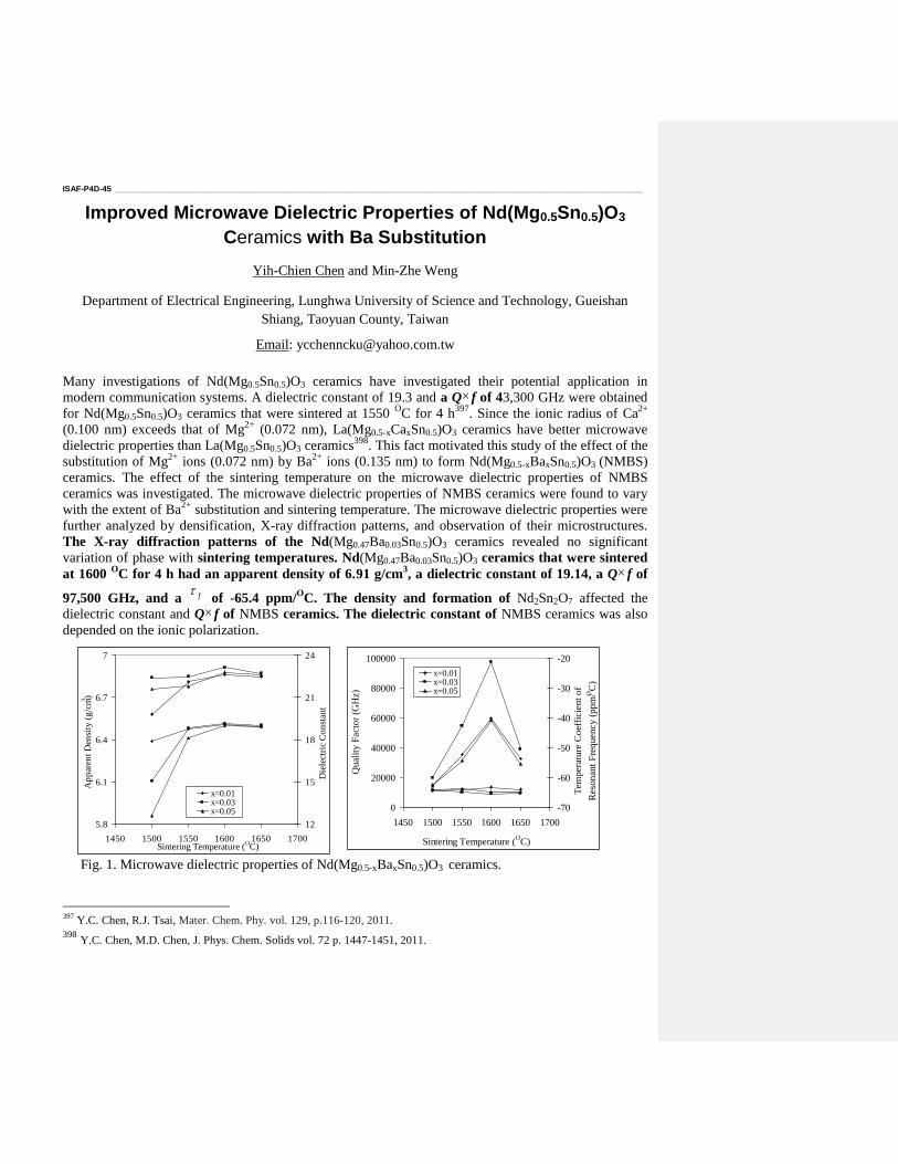
ISAF-P4D-45 ___________________________________________________________________________________________________________________
Improved Microwave Dielectric Properties of Nd(Mg0.5Sn0.5)O3
Ceramics with Ba Substitution
Yih-Chien Chen and Min-Zhe Weng
Department of Electrical Engineering, Lunghwa University of Science and Technology, Gueishan
Shiang, Taoyuan County, Taiwan
Email: [email protected]
Many investigations of Nd(Mg0.5Sn0.5)O3 ceramics have investigated their potential application in
modern communication systems. A dielectric constant of 19.3 and a Q f of 43,300 GHz were obtained
for Nd(Mg0.5Sn0.5)O3 ceramics that were sintered at 1550 OC for 4 h
397. Since the ionic radius of Ca
2+
(0.100 nm) exceeds that of Mg2+
(0.072 nm), La(Mg0.5-xCaxSn0.5)O3 ceramics have better microwave
dielectric properties than La(Mg0.5Sn0.5)O3 ceramics398
. This fact motivated this study of the effect of the
substitution of Mg2+
ions (0.072 nm) by Ba2+
ions (0.135 nm) to form Nd(Mg0.5-xBaxSn0.5)O3 (NMBS)
ceramics. The effect of the sintering temperature on the microwave dielectric properties of NMBS
ceramics was investigated. The microwave dielectric properties of NMBS ceramics were found to vary
with the extent of Ba2+
substitution and sintering temperature. The microwave dielectric properties were
further analyzed by densification, X-ray diffraction patterns, and observation of their microstructures.
The X-ray diffraction patterns of the Nd(Mg0.47Ba0.03Sn0.5)O3 ceramics revealed no significant
variation of phase with sintering temperatures. Nd(Mg0.47Ba0.03Sn0.5)O3 ceramics that were sintered
at 1600 O
C for 4 h had an apparent density of 6.91 g/cm3, a dielectric constant of 19.14, a Q f of
97,500 GHz, and a f of -65.4 ppm/O
C. The density and formation of Nd2Sn2O7 affected the
dielectric constant and Q f of NMBS ceramics. The dielectric constant of NMBS ceramics was also
depended on the ionic polarization.
5.8
6.1
6.4
6.7
7
1450 1500 1550 1600 1650 1700Sintering Temperature (
OC)
Ap
par
ent
Den
sity
(g
/cm3
)
12
15
18
21
24
Die
lect
ric
Co
nst
ant
x=0.01x=0.03x=0.05x=0.01x=0.03x=0.05
0
20000
40000
60000
80000
100000
1450 1500 1550 1600 1650 1700
Sintering Temperature (O
C)
Qual
ity F
acto
r (G
Hz)
-70
-60
-50
-40
-30
-20
Tem
per
ature
Coef
fici
ent
of
Res
onant
Fre
quency
(ppm
/OC
)
x=0.01x=0.03x=0.05x=0.01x=0.03x=0.05
Fig. 1. Microwave dielectric properties of Nd(Mg0.5-xBaxSn0.5)O3 ceramics.
397
Y.C. Chen, R.J. Tsai, Mater. Chem. Phy. vol. 129, p.116-120, 2011.
398 Y.C. Chen, M.D. Chen, J. Phys. Chem. Solids vol. 72 p. 1447-1451, 2011.
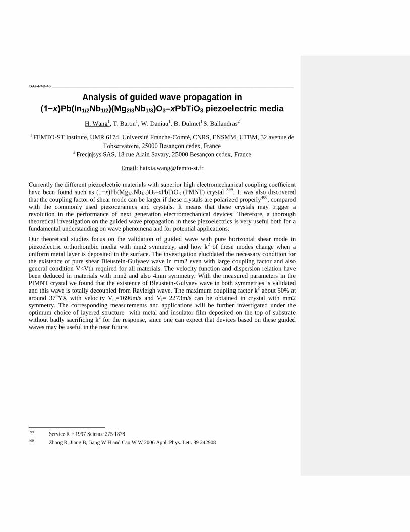
ISAF-P4D-46 ___________________________________________________________________________________________________________________
Analysis of guided wave propagation in
(1−x)Pb(In1/2Nb1/2)(Mg2/3Nb1/3)O3–xPbTiO3 piezoelectric media
H. Wang1, T. Baron
1, W. Daniau
1, B. Dulmet
1 S. Ballandras
2
1 FEMTO-ST Institute, UMR 6174, Université Franche-Comté, CNRS, ENSMM, UTBM, 32 avenue de
l’observatoire, 25000 Besançon cedex, France 2
Frec|n|sys SAS, 18 rue Alain Savary, 25000 Besançon cedex, France
Email: [email protected]
Currently the different piezoelectric materials with superior high electromechanical coupling coefficient
have been found such as (1−x)Pb(Mg1/3Nb1/3)O3–xPbTiO3 (PMNT) crystal 399
. It was also discovered
that the coupling factor of shear mode can be larger if these crystals are polarized properly400
, compared
with the commonly used piezoceramics and crystals. It means that these crystals may trigger a
revolution in the performance of next generation electromechanical devices. Therefore, a thorough
theoretical investigation on the guided wave propagation in these piezoelectrics is very useful both for a
fundamental understanding on wave phenomena and for potential applications.
Our theoretical studies focus on the validation of guided wave with pure horizontal shear mode in
piezoelectric orthorhombic media with mm2 symmetry, and how k2 of these modes change when a
uniform metal layer is deposited in the surface. The investigation elucidated the necessary condition for
the existence of pure shear Bleustein-Gulyaev wave in mm2 even with large coupling factor and also
general condition V<Vth required for all materials. The velocity function and dispersion relation have
been deduced in materials with mm2 and also 4mm symmetry. With the measured parameters in the
PIMNT crystal we found that the existence of Bleustein-Gulyaev wave in both symmetries is validated
and this wave is totally decoupled from Rayleigh wave. The maximum coupling factor k2 about 50% at
around 37oYX with velocity Vm=1696m/s and Vf= 2273m/s can be obtained in crystal with mm2
symmetry. The corresponding measurements and applications will be further investigated under the
optimum choice of layered structure with metal and insulator film deposited on the top of substrate
without badly sacrificing k2 for the response, since one can expect that devices based on these guided
waves may be useful in the near future.
399
Service R F 1997 Science 275 1878 400
Zhang R, Jiang B, Jiang W H and Cao W W 2006 Appl. Phys. Lett. 89 242908
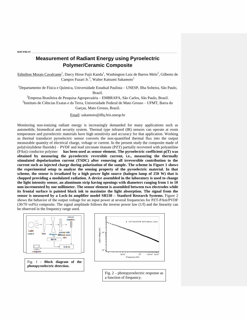
ISAF-P4D-47 ___________________________________________________________________________________________________________________
Measurement of Radiant Energy using Pyroelectric
Polymer/Ceramic Composite
Edinilton Morais Cavalcante1, Darcy Hiroe Fujii Kanda
1, Washington Luiz de Barros Melo
2, Gilberto de
Campos Fuzari Jr.3, Walter Katsumi Sakamoto
1
1Departamento de Física e Química, Universidade Estadual Paulista – UNESP, Ilha Solteira, São Paulo,
Brazil. 2Empresa Brasileira de Pesquisa Agropecuária – EMBRAPA, São Carlos, São Paulo, Brazil.
3Instituto de Ciências Exatas e da Terra, Universidade Federal de Mato Grosso – UFMT, Barra do
Garças, Mato Grosso, Brazil.
Email: [email protected]
Monitoring non-ionizing radiant energy is increasingly demanded for many applications such as
automobile, biomedical and security system. Thermal type infrared (IR) sensors can operate at room
temperature and pyroelectric materials have high sensitivity and accuracy for that application. Working
as thermal transducer pyroelectric sensor converts the non-quantified thermal flux into the output
measurable quantity of electrical charge, voltage or current. In the present study the composite made of
poly(vinylidene fluoride) – PVDF and lead zirconate titanate (PZT) partially recovered with polyaniline
(PAni) conductor polymer has been used as sensor element. The pyroelectric coefficient p(T) was
obtained by measuring the pyroelectric reversible current, i.e., measuring the thermally
stimulated depolarization current (TSDC) after removing all irreversible contribution to the
current such as injected charge during polarization of the sample. The scheme in Figure 1 shows
the experimental setup to analyze the sensing property of the pyroelectric material. In that
scheme, the sensor is irradiated by a high power light source (halogen lamp of 250 W) that is
chopped providing a modulated radiation. A device assembled in the laboratory is used to change
the light intensity sensor, an aluminum strip having openings with diameters ranging from 1 to 10
mm incremented by one millimeter. The sensor element is assembled between two electrodes while
its frontal surface is painted black ink to maximize the light absorption. The signal from the
sensor is measured by a Lock-In amplifier model SR530 – Stanford Research Systems. Figure 2
shows the behavior of the output voltage for an input power at several frequencies for PZT-PAni/PVDF
(30/70 vol%) composite. The signal amplitude follows the inverse power law (1/f) and the linearity can
be observed in the frequency range used.
5x10
110
21,5x10
22x10
2
100
101
PZT-PAni/PVDF 30/70 5MV/m, 15min
ou
tpu
t vo
ltag
e (
mV
)
Frequency (Hz)
Fig. 1 - Block diagram of the
photopyroelectric detection.
Fig. 2 – photopyroelectric response as
a function of frequency.
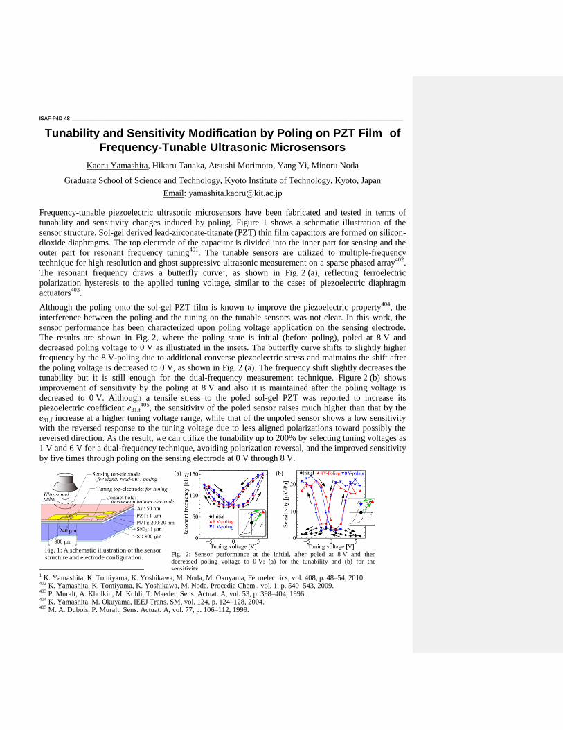
ISAF-P4D-48 ___________________________________________________________________________________________________________________
Tunability and Sensitivity Modification by Poling on PZT Film of
Frequency-Tunable Ultrasonic Microsensors
Kaoru Yamashita, Hikaru Tanaka, Atsushi Morimoto, Yang Yi, Minoru Noda
Graduate School of Science and Technology, Kyoto Institute of Technology, Kyoto, Japan
Email: [email protected]
Frequency-tunable piezoelectric ultrasonic microsensors have been fabricated and tested in terms of
tunability and sensitivity changes induced by poling. Figure 1 shows a schematic illustration of the
sensor structure. Sol-gel derived lead-zirconate-titanate (PZT) thin film capacitors are formed on silicon-
dioxide diaphragms. The top electrode of the capacitor is divided into the inner part for sensing and the
outer part for resonant frequency tuning401
. The tunable sensors are utilized to multiple-frequency
technique for high resolution and ghost suppressive ultrasonic measurement on a sparse phased array402
.
The resonant frequency draws a butterfly curve1, as shown in Fig. 2 (a), reflecting ferroelectric
polarization hysteresis to the applied tuning voltage, similar to the cases of piezoelectric diaphragm
actuators403
.
Although the poling onto the sol-gel PZT film is known to improve the piezoelectric property404
, the
interference between the poling and the tuning on the tunable sensors was not clear. In this work, the
sensor performance has been characterized upon poling voltage application on the sensing electrode.
The results are shown in Fig. 2, where the poling state is initial (before poling), poled at 8 V and
decreased poling voltage to 0 V as illustrated in the insets. The butterfly curve shifts to slightly higher
frequency by the 8 V-poling due to additional converse piezoelectric stress and maintains the shift after
the poling voltage is decreased to 0 V, as shown in Fig. 2 (a). The frequency shift slightly decreases the
tunability but it is still enough for the dual-frequency measurement technique. Figure 2 (b) shows
improvement of sensitivity by the poling at 8 V and also it is maintained after the poling voltage is
decreased to 0 V. Although a tensile stress to the poled sol-gel PZT was reported to increase its
piezoelectric coefficient e31,f405
, the sensitivity of the poled sensor raises much higher than that by the
e31,f increase at a higher tuning voltage range, while that of the unpoled sensor shows a low sensitivity
with the reversed response to the tuning voltage due to less aligned polarizations toward possibly the
reversed direction. As the result, we can utilize the tunability up to 200% by selecting tuning voltages as
1 V and 6 V for a dual-frequency technique, avoiding polarization reversal, and the improved sensitivity
by five times through poling on the sensing electrode at 0 V through 8 V.
1 K. Yamashita, K. Tomiyama, K. Yoshikawa, M. Noda, M. Okuyama, Ferroelectrics, vol. 408, p. 48–54, 2010.
402 K. Yamashita, K. Tomiyama, K. Yoshikawa, M. Noda, Procedia Chem., vol. 1, p. 540–543, 2009.
403 P. Muralt, A. Kholkin, M. Kohli, T. Maeder, Sens. Actuat. A, vol. 53, p. 398–404, 1996.
404 K. Yamashita, M. Okuyama, IEEJ Trans. SM, vol. 124, p. 124–128, 2004.
405 M. A. Dubois, P. Muralt, Sens. Actuat. A, vol. 77, p. 106–112, 1999.
Fig. 1: A schematic illustration of the sensor structure and electrode configuration.
Fig. 2: Sensor performance at the initial, after poled at 8 V and then decreased poling voltage to 0 V; (a) for the tunability and (b) for the sensitivity.
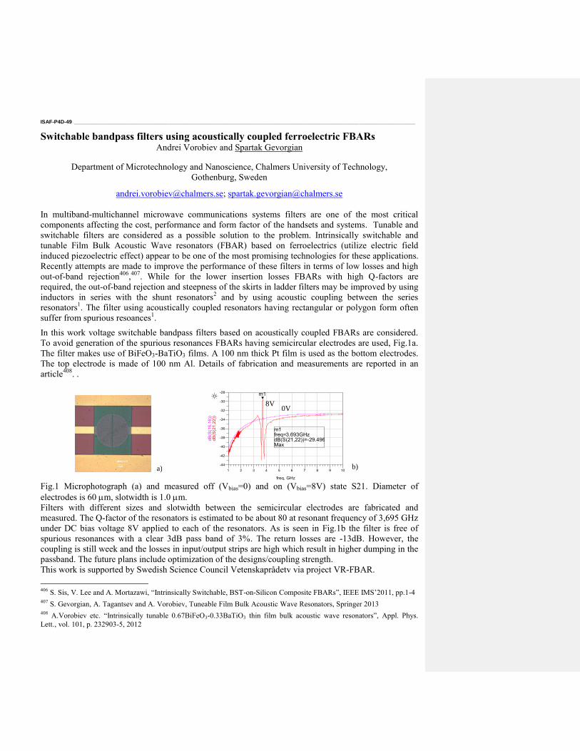
ISAF-P4D-49 ___________________________________________________________________________________________________________________
Switchable bandpass filters using acoustically coupled ferroelectric FBARs Andrei Vorobiev and Spartak Gevorgian
Department of Microtechnology and Nanoscience, Chalmers University of Technology,
Gothenburg, Sweden
[email protected]; [email protected]
In multiband-multichannel microwave communications systems filters are one of the most critical
components affecting the cost, performance and form factor of the handsets and systems. Tunable and
switchable filters are considered as a possible solution to the problem. Intrinsically switchable and
tunable Film Bulk Acoustic Wave resonators (FBAR) based on ferroelectrics (utilize electric field
induced piezoelectric effect) appear to be one of the most promising technologies for these applications.
Recently attempts are made to improve the performance of these filters in terms of low losses and high
out-of-band rejection406
,407
. While for the lower insertion losses FBARs with high Q-factors are
required, the out-of-band rejection and steepness of the skirts in ladder filters may be improved by using
inductors in series with the shunt resonators2 and by using acoustic coupling between the series
resonators1. The filter using acoustically coupled resonators having rectangular or polygon form often
suffer from spurious resoances1.
In this work voltage switchable bandpass filters based on acoustically coupled FBARs are considered.
To avoid generation of the spurious resonances FBARs having semicircular electrodes are used, Fig.1a.
The filter makes use of BiFeO3-BaTiO3 films. A 100 nm thick Pt film is used as the bottom electrodes.
The top electrode is made of 100 nm Al. Details of fabrication and measurements are reported in an
article408
. .
Fig.1 Microphotograph (a) and measured off (Vbias=0) and on (Vbias=8V) state S21. Diameter of
electrodes is 60 m, slotwidth is 1.0 m.
Filters with different sizes and slotwidth between the semicircular electrodes are fabricated and
measured. The Q-factor of the resonators is estimated to be about 80 at resonant frequency of 3,695 GHz
under DC bias voltage 8V applied to each of the resonators. As is seen in Fig.1b the filter is free of
spurious resonances with a clear 3dB pass band of 3%. The return losses are -13dB. However, the
coupling is still week and the losses in input/output strips are high which result in higher dumping in the
passband. The future plans include optimization of the designs/coupling strength.
This work is supported by Swedish Science Council Vetenskaprådetv via project VR-FBAR.
406
S. Sis, V. Lee and A. Mortazawi, “Intrinsically Switchable, BST-on-Silicon Composite FBARs”, IEEE IMS’2011, pp.1-4 407
S. Gevorgian, A. Tagantsev and A. Vorobiev, Tuneable Film Bulk Acoustic Wave Resonators, Springer 2013 408
A.Vorobiev etc. “Intrinsically tunable 0.67BiFeO3-0.33BaTiO3 thin film bulk acoustic wave resonators”, Appl. Phys.
Lett., vol. 101, p. 232903-5, 2012
a) b)
8V 0V
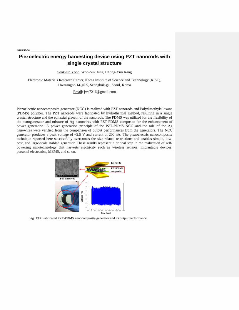
ISAF-P4D-50 ___________________________________________________________________________________________________________________
Piezoelectric energy harvesting device using PZT nanorods with
single crystal structure
Seok-Jin Yoon, Woo-Suk Jung, Chong-Yun Kang
Electronic Materials Research Center, Korea Institute of Science and Technology (KIST),
Hwarangno 14-gil 5, Seongbuk-gu, Seoul, Korea
Email: [email protected]
Piezoelectric nanocomposite generator (NCG) is realized with PZT nanorods and Polydimethylsiloxane
(PDMS) polymer. The PZT nanorods were fabricated by hydrothermal method, resulting in a single
crystal structure and the epitaxial growth of the nanorods. The PDMS was utilized for the flexibility of
the nanogenerator and mixture of Ag nanowires with PZT-PDMS composite for the enhancement of
power generation. A power generation principle of the PZT-PDMS NCG and the role of the Ag
nanowires were verified from the comparison of output performances from the generators. The NCC
generator produces a peak voltage of ~2.5 V and current of 200 nA. The piezoelectric nanocomposite
technique reported here successfully overcomes the size-related restrictions and enables simple, low-
cost, and large-scale stabled generator. These results represent a critical step in the realization of self-
powering nanotechnology that harvests electricity such as wireless sensors, implantable devices,
personal electronics, MEMS, and so on.
Fig. 133: Fabricated PZT-PDMS nanocomposite generator and its output performance.
ISAF-P4D-51 ___________________________________________________________________________________________________________________
Remanent polarization and electromechanical properties of LTCC-
PZT monomorphs
Sobocinski Maciej, Juuti Jari, Jantunen Heli
Microelectronics and Materials Physics Laboratories, University of Oulu, Finland
Email: [email protected]
Poling is a crucial stage in polycrystalline ceramic in order to exhibit piezoelectric properties. In the case
of Low Temperature Co-fired Ceramic embedded piezoelectric bulk structures, poling is necessary step
of manufacturing as elevated temperature of the process is far above the Curie temperature of common
PZT compositions. In previous works by the authors409410411
, LTCC embedded structures were poled
with 1.6 kV/mm and higher fields were restricted by occurring electrical breakdown during the poling.
Although sufficient remanent polarization has been obtained, further improvement of poling should be
emphasized. This paper focuses on optimization of the poling conditions for LTCC-PZT unimorph
structures. The problem of occurring electrical breakdown has been solved by applying additional
dielectric layer at the edges of the structure. Hysteresis measurements were done from 0.1 V/µm to 3
V/µm for three temperatures: 25 °C, 75 °C and 125 °C. Remanent polarization of 22 µC/cm2 was
obtained for the monomorph structure with 3.7 V/µm poling field at 125 °C. Subsequently LTCC-PZT
samples were poled in the optimal conditions and electrical and electro-mechanical properties was
measured and compared to previous results. Higher remanent polarization and planar coupling effect
was obtained.
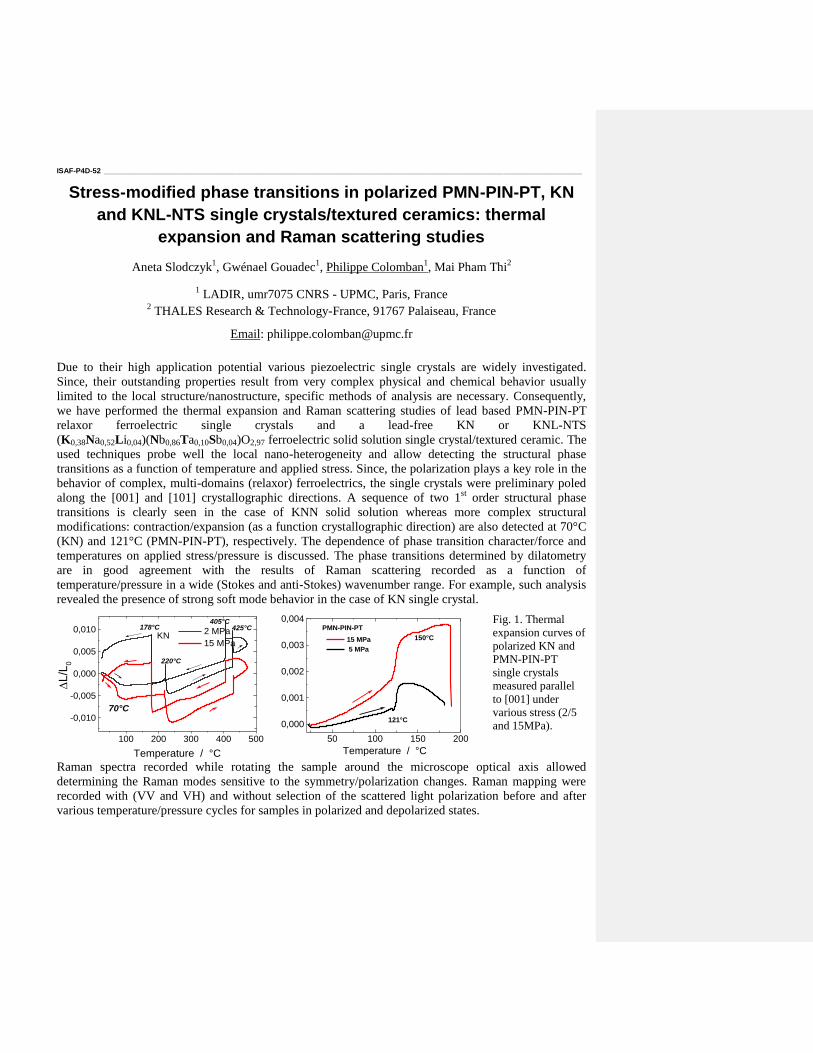
ISAF-P4D-52 ___________________________________________________________________________________________________________________
Stress-modified phase transitions in polarized PMN-PIN-PT, KN
and KNL-NTS single crystals/textured ceramics: thermal
expansion and Raman scattering studies
Aneta Slodczyk1, Gwénael Gouadec
1, Philippe Colomban
1, Mai Pham Thi
2
1 LADIR, umr7075 CNRS - UPMC, Paris, France
2 THALES Research & Technology-France, 91767 Palaiseau, France
Email: [email protected]
Due to their high application potential various piezoelectric single crystals are widely investigated.
Since, their outstanding properties result from very complex physical and chemical behavior usually
limited to the local structure/nanostructure, specific methods of analysis are necessary. Consequently,
we have performed the thermal expansion and Raman scattering studies of lead based PMN-PIN-PT
relaxor ferroelectric single crystals and a lead-free KN or KNL-NTS
(K0,38Na0,52Li0,04)(Nb0,86Ta0,10Sb0,04)O2,97 ferroelectric solid solution single crystal/textured ceramic. The
used techniques probe well the local nano-heterogeneity and allow detecting the structural phase
transitions as a function of temperature and applied stress. Since, the polarization plays a key role in the
behavior of complex, multi-domains (relaxor) ferroelectrics, the single crystals were preliminary poled
along the [001] and [101] crystallographic directions. A sequence of two 1st order structural phase
transitions is clearly seen in the case of KNN solid solution whereas more complex structural
modifications: contraction/expansion (as a function crystallographic direction) are also detected at 70°C
(KN) and 121°C (PMN-PIN-PT), respectively. The dependence of phase transition character/force and
temperatures on applied stress/pressure is discussed. The phase transitions determined by dilatometry
are in good agreement with the results of Raman scattering recorded as a function of
temperature/pressure in a wide (Stokes and anti-Stokes) wavenumber range. For example, such analysis
revealed the presence of strong soft mode behavior in the case of KN single crystal.
100 200 300 400 500
-0,010
-0,005
0,000
0,005
0,010405°C
178°C
70°C
425°C
220°C
2 MPa
15 MPaKN
L
/L0
Temperature / °C
50 100 150 200
0,000
0,001
0,002
0,003
0,004
L
/L0
Temperature / °C
PMN-PIN-PT
150°C 15 MPa
5 MPa
121°C
Fig. 1. Thermal
expansion curves of
polarized KN and
PMN-PIN-PT
single crystals
measured parallel
to [001] under
various stress (2/5
and 15MPa).
Raman spectra recorded while rotating the sample around the microscope optical axis allowed
determining the Raman modes sensitive to the symmetry/polarization changes. Raman mapping were
recorded with (VV and VH) and without selection of the scattered light polarization before and after
various temperature/pressure cycles for samples in polarized and depolarized states.
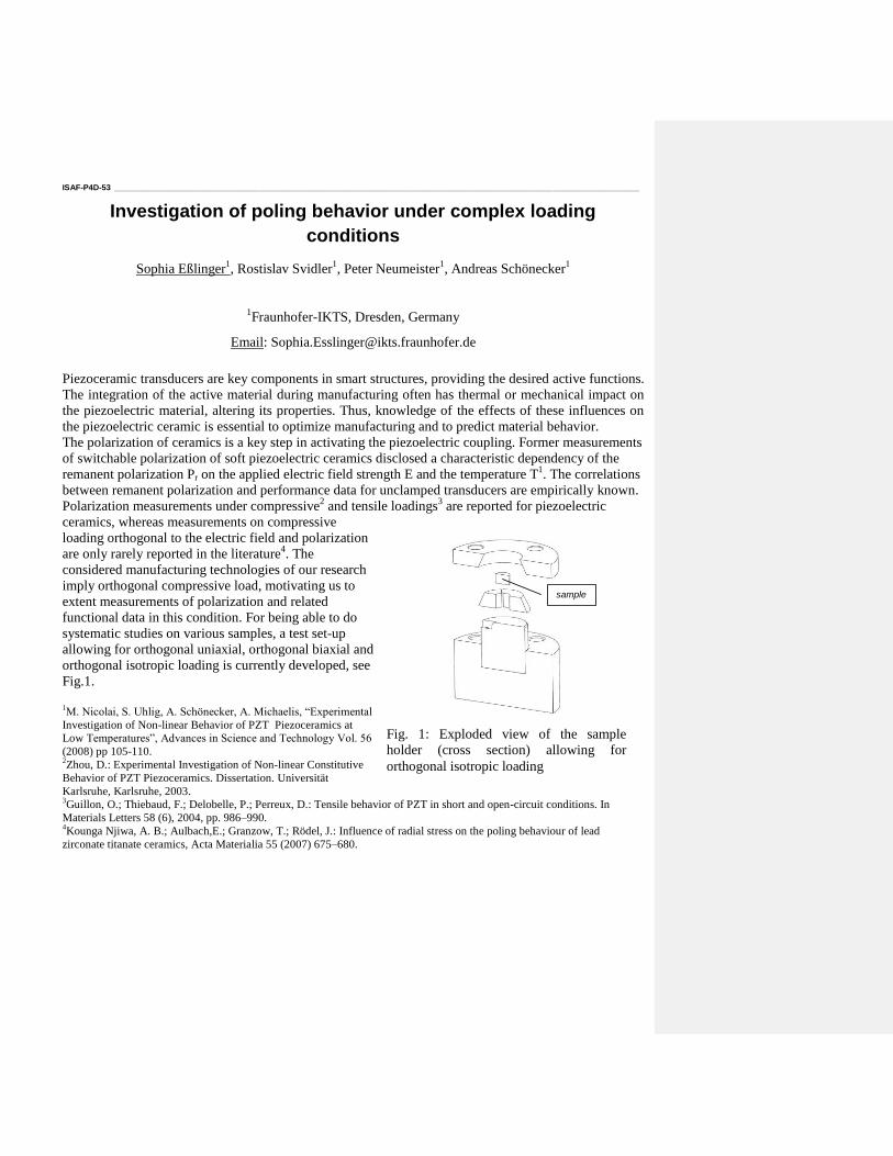
ISAF-P4D-53 ___________________________________________________________________________________________________________________
Investigation of poling behavior under complex loading
conditions
Sophia Eßlinger1, Rostislav Svidler
1, Peter Neumeister
1, Andreas Schönecker
1
1Fraunhofer-IKTS, Dresden, Germany
Email: [email protected]
Piezoceramic transducers are key components in smart structures, providing the desired active functions.
The integration of the active material during manufacturing often has thermal or mechanical impact on
the piezoelectric material, altering its properties. Thus, knowledge of the effects of these influences on
the piezoelectric ceramic is essential to optimize manufacturing and to predict material behavior.
The polarization of ceramics is a key step in activating the piezoelectric coupling. Former measurements
of switchable polarization of soft piezoelectric ceramics disclosed a characteristic dependency of the
remanent polarization Pr on the applied electric field strength E and the temperature T1. The correlations
between remanent polarization and performance data for unclamped transducers are empirically known.
Polarization measurements under compressive2 and tensile loadings
3 are reported for piezoelectric
ceramics, whereas measurements on compressive
loading orthogonal to the electric field and polarization
are only rarely reported in the literature4. The
considered manufacturing technologies of our research
imply orthogonal compressive load, motivating us to
extent measurements of polarization and related
functional data in this condition. For being able to do
systematic studies on various samples, a test set-up
allowing for orthogonal uniaxial, orthogonal biaxial and
orthogonal isotropic loading is currently developed, see
Fig.1.
1M. Nicolai, S. Uhlig, A. Schönecker, A. Michaelis, “Experimental
Investigation of Non-linear Behavior of PZT Piezoceramics at
Low Temperatures”, Advances in Science and Technology Vol. 56
(2008) pp 105-110. 2Zhou, D.: Experimental Investigation of Non-linear Constitutive
Behavior of PZT Piezoceramics. Dissertation. Universität
Karlsruhe, Karlsruhe, 2003. 3Guillon, O.; Thiebaud, F.; Delobelle, P.; Perreux, D.: Tensile behavior of PZT in short and open-circuit conditions. In
Materials Letters 58 (6), 2004, pp. 986–990. 4Kounga Njiwa, A. B.; Aulbach,E.; Granzow, T.; Rödel, J.: Influence of radial stress on the poling behaviour of lead
zirconate titanate ceramics, Acta Materialia 55 (2007) 675–680.
Fig. 1: Exploded view of the sample
holder (cross section) allowing for
orthogonal isotropic loading
sample
ISAF-P4D-54 ___________________________________________________________________________________________________________________
Stability study of [011] ternary PIN-PMN-PT relaxor ferroelectric single crystals under high electric field and compressive stress
Th.Pastureaud1, M. Dosiy
1, F-X Launay
1, R. Thannberger
1, P. Finkel
2, H. Robinson
2, J. State
2,
C.Murphy2, E. Leveugle
3 and M. Pham-Ti
3
1Thales Underwater System, Acoustic & Mechanical Competence Centre, 525 route des dolines, BP
157, 06903 Sophia-Antipolis cedex, France 2Naval Undersea Warfare Center - Devices, Sensors & Materials R&D, 1176 Howell Street, Newport,
RI 02841 3Thales Research and Technology, Campus Polytechnique, 1 Avenue Auguste Fresnel, 91767 Palaiseau
Cedex, France
Email: [email protected]
Piezoelectric properties of [011] poled 32 mode 24PIN-48PMN-28PT single crystals have been studied
under temperature, large stress and electric field. Dielectric drift measurement shows good stability up
to field of 350 Vrms/mm, which appears consistent with polarization field loop measured at room
temperature. Room temperature elastic and piezoelectric responses, measured independently, display
strong and sharp discontinuity at approximately 17 MPa compressive stress that is associated with the
stress induced phase transition. These results agree with previous data supporting the conclusion that in
ternaries this instability is likely related to the ferroelectric rhombohedral (R) – orthorhombic (O) phase
transition. In good agreement with existing model, we observe the destabilization of the (R) phase by
applying DC electric field along the poling direction. Stability stress-field-temperature diagrams
defining the linear regions for the crystal are constructed.
ISAF-P4D-55 ___________________________________________________________________________________________________________________
PZT materials with compositions at the morphotropic phase boundary (MPB) between the tetragonal
(P4mm) and rhombohedral (R3m) phase fields exhibit very high dielectric and piezoelectric properties
which are intensively used for technological applications (sensors and actuators, microelectromechanical
systems, and high frequency devices) [1]. We recently reported an in situ description of the origin of the
ferroelectric properties as a function of the applied electric field E based on a synchrotron X-ray
diffraction study [2]. The monoclinic (pseudo-rhombohedral)/ tetragonal phase ratio was found to
increase with electric field which strongly supported the hypothesis of Noheda et al., who explained the
strong piezoelectric properties of PZT by the presence of a monoclinic phase [3] based on a polarization
rotation mechanism [4]. Additionally, polarization flipping of polar lead atoms could unambiguously be
characterized by a maximum in the disorder of lead (Biso(Pb)m) for the positive-negative value of the
coercive field (Ec) in the PS - E hysteresis cycle. Here, we present a structural description of the
macroscopic piezo- and ferroelectric properties in the important technological material Lead Zirconate
Titanate (PZT) by in situ synchrotron X-ray and Neutron diffraction. In addition to a technically applied
material, we investigated the poling behavior of different composition series in the vicinity of the MPB.
The structural changes were either induced by variations of the lead oxide content during sintering or
different titanium / zirconium ratios. Stroboscopic pump-probe measurements down to 250 μs time
resolution reveal differences in poling kinetics depending on composition. For the technically applied
material they spectacularly comfort our interpretations and clearly show the time structure characterizing
the ferroelectric poling response.
[1] B. Jaffe, W. R. Cook, H. Jaffe, Piezoelectric Ceramics, Academic, London (1971).
[2] M. Hinterstein et al. Phys. Rev. Lett. 107, 077602 (2011).
[3] B. Noheda, D. E. Cox, G. Shirane, J. A. Gonzalo, L. E. Cross, and S.-E. Park, Appl. Phys. Lett. 74,
2059 (1999).
[4] R. Guo, L. E. Cross, S.-E. Park, B. Noheda, D. E. Cox, and G. Shirane, Phys. Rev. Lett. 84, 5423
(2000).
ISAF-P4D-56 ___________________________________________________________________________________________________________________
Study on Electric-field induced Strain and Dielectric Properties of
PMN-PT Ceramics
Wei Zhao1,2
, Wei Ruan1, Lizhu Huang
1,2, Jiangtao Zeng
1, Liaoying Zheng, Huarong Zeng, Guorong Li
1
1Shanghai Institute of Ceramics, Chinese Academy of Sciences, Shanghai, China
2University of Chinese Academy of Sciences, Beijing, China
E-mail: [email protected]
The (1-x)PMN-xPT (0.1≤x≤0.35) ceramics were prepared by columbite method. The correlation of the
ferroelectric/piezoelectric properties with domain structure was studied systemically. As the PT content
increases, the ferroelectric state of PMN-PT system transforms gradually from the relaxor ferroelectric
state to the normal ferroelectric state, accompanied with the change of electric-field induced strain,
ferroelectric and dielectric properties. Electric-field induced strain reaches the maximum value of 0.25%
at 32 kV/cm for the sample 70/30 due to its piezoelectric character. The P-E loop and dielectric property
of (1-x)PMN-xPT clarify domain’s contribution to the large strain. The dielectric behavior is found to
have a thermal hysteresis due to the hysteresis of domains state changing between microdomain and
macrodomain.
ISAF-P4D-57 ___________________________________________________________________________________________________________________
Temperature-Dependent Strain Properties of Nb-doped
Bi1/2(Na0.84K0.16)1/2TiO3 –SrTiO3 Lead-Free Piezoelectrics
Rizwan Malik1, Thi Hinh Dinh
1, Changhyo Hong
1, Hyoung-Su Han
1, Wook Jo
2, Ali Hussain
3 and Jae-
Shin Lee1
1School of Material Science and Engineering, University of Ulsan, Ulsan, Republic of Korea
2Institute of Materials Science, Technische Universität Darmstadt, Darmstadt, Germany
3School of Nano and Advanced Materials Engineering, Changwon National University, Gyeongnam,
Republic of Korea
Email: [email protected]
Recently, 0.82(Bi1/2Na1/2)TiO3-0.18(Bi1/2K1/2)TiO3 solid solution (BNKT) ceramics and their modified
ones have attracted great attention because of their large electric field-induced strains (EFIS). However,
BNKT retains a crucial problem of showing high strain values only near room temperature. Meanwhile,
actuators for practical applications are required to maintain high strain over a wide temperature range
dependent on their operating environment and self-heating.
In this study, lead-free 0.96[Bi1/2(Na0.84K0.16)1/2TiO3]–0.04SrTiO3 (BNKT-ST) ceramics and Nb-doped
BNKT-ST (BNKNT-ST) were fabricated by the conventional solid-state method, and their dielectric and
piezoelectric properties were investigated as functions of Nb doping level and temperature. The
normalized strain (Smax/Emax) of BNKT-ST was 246 pm/V at room temperature, rapidly increased up to
110oC, and reached its highest value of 742 pm/V. In contrast, the BNKTN-ST showed quite different
Smax/Emax values compared with BNKT-ST. The Smax/Emax was started as 726 pm/V at room temperature.
After that, as rising temperature it decreased gradually and the value was still remaining 560 pm/V at
110oC.
Fig. 134: Comparison of temperature dependence of Smax/Emax between
undoped and Nb-doped BNKT-ST ceramics.
ISAF-P4D-58 ___________________________________________________________________________________________________________________
Comparative study of electrical properties of PbLaZrTiOx
capacitors with Al-doped ZnO and ITO top electrodes
Yoko Takada, Toru Tsuji, Naoki Okamoto, Takeyasu Saito, Kazuo Kondo, Takeshi Yoshimuraa,
Norifumi Fujimuraa, Koji Higuchi
b, Akira Kitajima
b, and Akihiro Oshima
b
Dept. of Chem. Eng., Osaka Prefecture University, Sakai, Osaka, JAPAN a Dept. of Phys. Electro., Osaka Prefecture University, Sakai, Osaka, JAPAN
b Inst. of Sci. and Ind. Res., Osaka University, Ibaraki, Osaka, JAPAN
Email: [email protected]
Ferroelectric Random Access Memory (FeRAM) has attracted much attention and it is believed to be next
generation non-volatile memory for its high operation (read/write) speed and low power consumption1). For
example, the application of FeRAM includes transportation IC tags, mobile cards, and so on. However,
conventional noble metal electrodes for ferroelectric materials, Pt, Ir or IrO2, causes price and resource issues
for FeRAM device fabrication. In this study, we used conductive Al-doped ZnO (AZO)2) and Sn-doped
In2O3 (ITO)3) as an alternative for Pt top electrodes of PbLa(Zr,Ti)O3 (PLZT) capacitors and evaluated the
ferroelectric properties.
The substrates were highly (111)-oriented sputtered Pt as lower electrodes. PLZT
(Pb:La:Zr:Ti=113:3:30:70) films (500 nm) were prepared by the sol-gel method. The films were deposited
on Pt substrate by spin coating, at 3000 rpm for 20 s. Then, the gel-films were dried at 200℃ for 2 min in
order to eliminate the solvent, and pyrolyzed at 300°C for 10 min, in air for organic components removal.
The films were prepared by repeating (3 times) the deposition and pyrolysis cycle. The prepared thickness
was 500 nm. The coated films were finally calcined in air at 750°C, 10 min, in air for achieving
crystallization. Pt top electrodes were deposited by sputtering. AZO and ITO top electrodes were deposited
by Pulsed Laser Deposition (PLD). These deposition were performed with a metal through mask having 50
um ~ 500 um diameter. The composition of AZO and ITO targets were ZnO:Al2O3=98.5:1.5 wt.% and
In2O3:SnO2=95.0:5.0 wt.%, respectively.
Initial polarization values of PLZT
capacitors with Pt, AZO and ITO as top
electrodes were 24.1 C/cm2, 20.2 C/cm2 and
16.2 C/cm2, respectively. Fig. 1 shows the
polarization ratio of PLZT capacitors with Pt,
AZO and ITO electrodes after heating in
200°C, 1 Torr, 3% hydrogen atmosphere. The
polarization ratio of PLZT capacitors with Pt
AZO and ITO electrodes after 45 minutes
were 0.23, 0.28, and 0.28, respectively. The
implementation of AZO was promising in
terms of hydrogen degradation.
References
1) M.M. Zhang et al., Solid-State Electronics, Vol. 53, p. 473 (2009).
2) A. Suzuki et al., Thin Solid Films, Vol. 517, p. 1478 (2008).
3) A.V. Rao et al., Materials Letters, Vol. 29, p. 255 (1996).
Fig. 1 Changes in polarization ratio of PLZT capacitors
with Pt, AZO and ITO top electrodes at 15 V.
ISAF-P4D-59 ___________________________________________________________________________________________________________________
Leakage Currents in Sol-Gel PZT Films
Alexander Sigov, Yury Podgorny, Konstantin Vorotilov, Alexey Vishnevskiy
Moscow State Technical University of Radioengineering, Electronics and Automation (MIREA),
Moscow, Russia
Email: [email protected]
Ferroelectrics are used in the capacitor structures of memory devices, therefore leakage currents and
electrical breakdown represent potential problems which should be solved to provide the required
operating characteristics. The study of the current–voltage (I–V) characteristics permits to obtain
information on charge transport mechanisms in PZT films and film-electrode interfaces.
Possible conduction mechanisms in ferroelectric films (dielectrics) are the Schottky and Poole–Frenkel
emissions, the Fowler–Nordheim tunneling, the ohmic, space–charge–limited, hopping conductivity, and
conductivity via the grain boundaries412,413
.
The objective of this research is to study the conduction mechanisms in PZT ferroelectric thin films
prepared by the sol–gel method on silicon substrates with platinum bottom electrode for different
voltage ramp speed and electric fields strengths. Long–term (tens of minutes) depolarization processes
in metal–ferroelectric–metal (MFM) structure are studied as well.
Main mechanisms of leakage currents in thin PZT ferroelectric films prepared by the sol–gel method are
discussed. Four specific regions are determined in I-V dependences. At very weak fields (10-20 kV/cm)
the current falls with the voltage increase as a result of depolarization. In the low field region (about 70-
100 kV/cm), the leakage current decreases with decreasing voltage ramp speed, and its components are
the ohmic and displacement currents. In the high field region (≥130 kV/cm) the leakage current
increases with decreasing step voltage ramp, in contrast to the previous case. Possible conductivity
mechanisms are the Pool-Frenkel emission and hopping conduction. In the transition region between
abovementioned ones (from 80–90 to ~130 kV/cm), an abrupt unstable current increase is observed
caused by breakdown of reverse bias Schottky barrier.
Depolarization current is given by a decreasing function which can be approximated by the sum of two
exponents with different relaxation times. As an example, depolarization currents for sol-gel PZT thin
films prepared at different annealing temperatures are studied. It is shown that both absolute and relative
values of depolarization currents are increased with the increase of annealing temperature caused by
film-substrate interface distortion.
412
R. Waser, M. Klee, “Theory of conduction and breakdown in perovskite thin films”, Integr. Ferroelectrics, vol. 2, p. 23–
40, 1992. 413
M. Dawber, K.M. Rabe, J.F. Scott, “Physics of thin–film ferroelectric oxides”, Rev. Mod. Phys., vol. 77, p. 1083–1130,
2005.
ISAF-P4D-60 ___________________________________________________________________________________________________________________
Simultaneous piezoelectric and ferroelectric characterization of thin films for MEMS actuators
Andrea Mazzalai1, Davide Balma
1, Nachiappan Chidambaram
1, Paul Muralt
1
1Ceramics Laboratory, École Polytechnique Fédérale de Lausanne – EPFL,
Lausanne, Switzerland
Email: [email protected]
Recent improvements of piezoelectric thin films, like lead zirconate titanate Pb(Zrx,Ti1-x)O3 (PZT), are
driven by high volume applications that will lead to an exponential increase of the piezo-MEMS market.
Many devices of interest like inkjet print-heads or autofocus lenses are actuators relying on the
transverse converse piezoelectric effect of ferroelectric thin films sandwiched between a parallel-plate
capacitor structure. For the purpose of film development, we need to measure the in-plane stress (T1)
and the ferroelectric polarization (P) loops. In this work, we have set up a cheap, versatile and easy to
use tool that is based on an optical probe, a charge amplifier, a XYZ manipulator stage, and suitable
cantilever samples that may have the full wafer thickness. The derivative of the obtained stress loop
gives directly the converse piezoelectric coefficient e31, f = ¶T1 / ¶E3at a given voltage for an arbitrary
waveform.
Figure 135. Simultaneous measurement of
polarization and stress loops at a sol-gel deposited
PZT thin film. The curves are averages of 500
continuous cycles made at a repetition rate of
110Hz.
Figure 136. Numerical derivative of the averaged
stress loop yields the effective converse
piezoelectric coefficient e31,f as a function of the
electric field.
Figure 1 shows the measurement obtained with a 1.18μm thick, sol-gel PZT thin film annealed after top
electrode deposition. The remnant effective piezoelectric coefficient e31,f was measured as 14.7 C/m2
with this set-up, and is identical to the direct e31,f measured with the set up for the direct effect (as
explained in refs 414
,415
). We shall present the calculation of the in-plane stress from the cantilever
deflection and report on a detailed study about the impact of the sample geometry and set-up parameters
on accuracy and precision of the measurement.
414
Dubois et. al. Sensors and Actuator A 77 (1999), p. 106 415
Ledermann et. al. Sensors and Actuators A 105 (2003), p 162

ISAF-P4D-61 ___________________________________________________________________________________________________________________
Effect of Polarization on Mechanical Properties of PZT Ceramics
Yao Yu, Xusheng Wang, Xi Yao
Functional Materials Research Laboratory, Tongji University, 1239 Siping Road, Shanghai200092, PR
China
Email: [email protected]
Abstract: The dynamic mechanical properties (storage modulus and internal friction) of PZT-5H and
PZT-8 ceramics with temperature were investigated before and after polarization at different vibration
load of 0.1, 0.5, 1, 5 and 10Hz by Dynamic Mechanical Analysis (DMA). The Curie temperature of
PZT-5H and PZT-8 ceramics tested by DMA are 438K and 548K. The relaxation peak emerges in
internal friction curves, and their position and intensity vary in different laws for PZT-5H and PZT-8.
The relaxation processes were studied according to Arrhenius law. The activation energies of
unpolarized and polarized PZT-5H ceramics are 1.29eV and 1.36eV, the activation energies of
unpolarized and polarized PZT-8 ceramics are 1.05eV and 1.08eV.
i F. Cordero, F. Trequattrini, F. Craciun, and C. Galassi, J Phys Condens Matter 23, 415901 (2011).
ii M. A. Carpenter, J. F. Bryson, G. Catalan, S. J. Zhang, and N. J. Donnelly, J Phys Condens Matter 24, 045902
(2012). iii W. Schranz, H. Kabelka, A. Sarras, and M. Burock, Applied Physics Letters 101, 141913 (2012).
iv A. Bouzid, E. M. Bourim, M. Gabbay, and G. Fantozzi, Journal of the European Ceramic Society 25, 3213
(2005). v S. A. T. Redfern, C. Wang, J. W. Hong, G. Catalan, and J. F. Scott, Journal of Physics-Condensed Matter 20,
452205 (2008). vi G. Picht, K. G. Webber, Y. Zhang, H. Kungl, D. Damjanovic, and M. J. Hoffmann, Journal of Applied Physics
112, 124101 (2012). vii
S. Sarkar, X. Ren, and K. Otsuka, Physical Review Letters 95, 205702 (2005). viii
E. Buixaderas, D. Nuzhnyy, J. Petzelt, L. Jin, and D. Damjanovic, Physical Review B 84, 184302 (2011). ix J. Weerasinghe, D. W. Wang, and L. Bellaiche, Physical Review B 85, 014301 (2012).
x M. Weihnacht, A. Sotnikov, H. Schmidt, E. Smirnova, and S. Ktitorov, Proceedings of the 2011 IEEE
International Symposium on Applications of Ferroelectrics (ISAF), Vancouver, July 2011. xi J. Hlinka, J. Petzelt, S. Kamba, D. Noujni, T. Ostapchuk, “Infrared dielectric response of relaxor
ferroelectrics”, Phase Transition,. vol. 101, pp. 167402(1-4), 2008. xii
F. Jona, G. Shirane, F. Mazzi, and R. Pepinsky, “X-Ray and Neutron diffraction study of
antiferroelectric lead zirconate, PbZrO3”, Phys. Rev., vol. 105, pp. 849-856, 1957. xiii T. Ostapchuk, J. Petzelt, V, Železný, S. Kamba, B. Malič, M. Kosec, L. Čakare, K. Roleder, J. Dec,
“Infrared spectroscopy of lead zirconate single crystal, ceramics and films”, Ferroelectrics , vol. 239,
pp.109-115, 2000. xiv T. Ostapchuk, J. Petzelt, V. Železný, S. Kamba, V. Bovtun, V. Porokhonskyy, A. Pashkin , P. Kuzel,
M.D. Glinchuk, I.P. Bykov, B. Gorshunov, M. Dressel, “Polar phonons and central mode in
antiferroelectric PbZrO3 ceramics”, J. Phys.: Condens. Matter, vol. 13, pp.2677–2689, 2001. xv J. Hlinka, T. Ostapchuk, D. Nuzhnyy, J. Petzelt, P. Kuzel, C. Kadlec, P. Vanek, I. Ponomareva, L.
Bellaiche, “Coexistence of the phonon and relaxation soft modes in the terahertz dielectric response of
tetragonal BaTiO3”, Phys. Rev. Lett., vol. 101, pp. 167402(1-4), 2008. xvi
Yang, S. Y.et al., Nature Nanotechnology, 2010, 5, 143-147 xvii Alexe, M., Nano Letters, 2012, 12, 2193-2198
xviii Matthias B. and Remeika J.P., Phys. Rev. 1949, 76, 1886.
xix Bollmann W. and Stöhr H.J., Physica Status Solidi A 1977, 39, 477.
xx Bagotsky V.S., Fundamentals of Electrochemistry; Wiley 2006.
1 V. Ya. Shur, E. L. Rumyantsev, S. D. Makarov, "Kinetics of phase transformations in real finite
systems: Application to switching in ferroelectrics", J. Appl. Phys., vol. 84, p. 445-451, 1998.
xxii J. Hlinka et al., , Phys. Rev. B, vol. 83, article no. 020101(R), 2011.
xxiii…
xxiv J. Hlinka, B. Hehlen, A. Kania and I. Gregora, “Soft mode in cubic PbTiO3 by hyper-Raman
scattering”, Phys. Rev. B, vol. 87, p. 064101 (1-4), 2013
xxv
I. Tomeno, J.A. Fernandez-Baca, K.J. Mary, K. Oka, Y. Tsunoda, “Simultaneous softening of
acoustic and optical modes in cubic PbTiO3”, Phys. Rev. B, vol. 86, p. 134306(1-15), 2012.
xxvi Goto, T., Kimura, T., Lawes, G., Ramirez, a. P., & Tokura, Y., Physical Review Letters, 92, 257201 (2004). xxvii Hu, C., Physical Review B, 77, 174418 (2008). xxviii Mochizuki, M., Furukawa, N., & Nagaosa, N,. Physical Review B, 84, 144409 (2011).
xxix K. Nakamura and H. Shimizu, Ferroelectrics 93, 211 (1989)
xxx V.D. Kugel, G. Rosenman, and D. Shur, J. Appl. Phys. 78, 5592 (1995).
xxxi A.A. Grekov, A.A. Adonin, N.P. Protsenko, Ferroelectrics 13, 483 (1976). xxxii J. Seidel, et al., Nature Materials 8, 229 (2009). xxxiii H. Ishizuki, I. Shoji and T. Taira, Appl. Phys. Lett. 82, 4062 (2003). xxxiv M. Schröder, et al., Adv. Funct. Mater. 22, 3936 (2012). xxxv V.Ya. Shur et al., Appl. Phys. Lett. 77, 3636 (2000).


