Embed Size (px)
Citation preview

1
A novel adaptive synchronous rectification systemfor low output voltage isolated converters
M. Rodrıguez, Student Member, IEEE, D. G. Lamar, Member, IEEE, M. Arias, Member, IEEE,R. Prieto, Member, IEEE and J. Sebastian, Member, IEEE
Abstract—The design of efficient, isolated low output voltageconverters is a major concern due to their widespread use. Oneof the preferred methods used to maximize their efficiency is syn-chronous rectification, i.e. the replacement of the secondary sidediodes with MOSFETs to decrease conduction losses. However,depending on the topology being used, synchronous rectificationmight not provide the required efficiency improvement or evenbe easily implemented. This paper presents a novel synchronousrectification system that can be applied to converters withsymmetrically-driven transformers and to converters from theFlyback family; in both cases, the proposed system adaptivelygenerates a control signal that controls a synchronous rectifierMOSFET placed in paralell with each diode, turning it on duringthe conduction intervals of the diodes. The proposed systemuses only information from the secondary side, thus avoidingbreaking the isolation barrier; it can be built using a few low costanalog components, it is reliable and simple, and could be easilyimplemented in an integrated circuit. Up to a 3 % improvementis demonstrated in a 3.3-5 V, 120 W Push-Pull converter and upto a 2.5 % improvement is obtained in a 5 V, 50 W Flybackconverter, both of them designed for telecom applications.
Index Terms—DC-DC power converters, Power conversion,Switching converters
I. INTRODUCTION
LOW output voltage converters are widely used in manyapplications. The supply of integrated circuits, micropro-
cessors and FPGAs is undoubtely one of the most important;said loads are usually supplied with voltages that can rangefrom 1.2 V to 5 V, thus demanding high output currents fromthe converter. To increase the efficiency of these converters,transistors must replace diodes in the rectification stage, ina technique usually called Synchronous Rectification (SR). Adetailed comparison between the use of diode rectifiers versussynchronous rectifiers can be found e.g. in [1].
In the majority of low output voltage applications, MOSFETtransistors are used as synchronous rectifiers, mainly due to
Manuscript received May 21, 2010. Accepted for publication October 9,2010.
Copyright c© 2010 IEEE. Personal use of this material is permitted.However, persmission to use this material for any other purposes must beobtained from the IEEE by sending a request to [email protected].
This work was supported by the Spanish Ministry of Science and Innovationunder grant AP2006-04777 and under the Consolider Project RUE CSD2009-00046.
M. Rodrıguez, D. G. Lamar, M. Arias and J. Sebastian are with theElectronic Power Supply Systems Group, Universidad de Oviedo. EdificioDepartamental 3, Campus de Viesques s/n, 33204 Gijon, Spain (contact e–mail: [email protected]).
R. Prieto is with the Centro de Electronica Industrial, UniversidadPolitecnica de Madrid, E. T. S. Ingenieros Industriales. C/ Jose GutierrezAbascal, 2. 28006 Madrid.
Primary side
switches
Synchronous
Rectification
stage
Output
filter
Control
Primary side
control signalsSync rectifiers
control signals
isolation
(a)
Primary side
switches
Synchronous
Rectification
stage
Output
filter
Control
Primary side
control signalsSelf-driven sync
rectification signals
(b)Figure 1. Isolated converter block diagram: (a) with EDSR; (b) withSDSR.
their low on-resistance that minimizes conduction losses. Themajor drawback regarding the use of synchronous rectifiers isthe need for a control signal that has to turn on the transistorduring the intervals when the diodes would be conducting,avoiding short circuits in the secondary side. Traditionally,two different techniques have been used to control the syn-chronous rectifiers [2]. The first one is called External-drivenSynchronous Rectification (EDSR) and it is shown in Fig.1a. In this technique, the control signals are generated by anauxiliar circuit that guarantees the appropriate timing, and thusthe transistors can be activated during the whole rectificationperiod and the efficiency can be maximized [3]. However,in isolated applications, the control signals that are usuallygenerated in the primary side have to be transmitted to thesecondary side, thus increasing complexity and cost.
Fig. 1b shows the second technique, called Self-driven Syn-chronous Rectification (SDSR). In SDSR the control signalsare obtained directly from the power stage; therefore, the spe-cific topology being used determines the conduction intervalsof the rectifiers. SDSR is preferred in isolated applicationsbecause the control signals are usually obtained directly fromthe power transformer, thus yielding a very simple, efficientand reliable rectification stage [4]–[6]. Several modificationsto the SDSR method have been proposed to improve itsperformance in certain applications [7]–[13], although the

2
complexity of some of the solutions finally led to a hybridscheme, as in [11], [12]. However, in many topologies thedriving signals cause the synchronous rectifiers to be off duringa certain part of the switching cycle, thus causing conductionof the parasitic diodes and decreasing efficiency. For instance,in topologies with symmetrically-driven transformers, as Half-bridge, Full-bridge and Push-Pull topologies, the synchronousrectifiers are not activated during the dead times of thetransformer. This fact causes a noticeable decrease in theefficiency for high input voltages (i.e. low duty cycles). Intelecom applications in which a wide input voltage range iscommon (18-36 V in rated 24 V converters and 36-72 V inrated 48 V converters), commercial products might suffer anefficiency drop as high as 4 % (see for instance the ASQ24family [14]). Several solutions have already been proposedto solve this problem [15]–[17]. Reference [15] proposes asystem based on additional windings to drive the synchronousrectifiers. It provides a very good performance but requiresa very careful magnetic design, which can compromise thebehavior of the system and increase the cost of the converter.References [16], [17] use an additional controlled voltagesource to force the synchronous rectifiers to be on during thedead times. This system also performs well, but again requiresa careful design of the voltage source, which in turn has to beregulated using extra circuitry that complicates the system.
This paper proposes a novel synchronous rectifica-tion scheme to be used in isolated converters that hasbeen called Adaptive Off-Time Synchronous Rectification(AOTSR). The proposed system extends the time interval whenthe synchronous rectifiers are activated in topologies withsymmetrically-driven transformers (Half and Full-bridges andPush-Pull) that implement SDSR. The system can also be usedas a complete synchronous rectification system in convertersfrom the Flyback family (Flyback, isolated SEPIC, Cuk andZeta). In this kind of applications the use of synchronousrectification has also been explored throughout custom cir-cuitry: [18] uses very simple analog circuitry to control asynchronous rectifier in a low cost Flyback converter, butonly when it operates in Discontinuous Conduction Mode(DCM). Several commercial ICs, as the IR11672 or theNCP4302, allow to control synchronous rectifiers using onlyinformation from the secondary side in Flyback and Half-Bridge converters, but the use of these ICs is currently not verywidespread. Furthermore, those ICs turn on or off the rectifiersby measuring the instantaneous voltage across it, thus havingrelatively high noise-sensitivity. With the use of additionalswitches in converters with symmetrically-driven transformerswith SDSR, and with a single switch in parallel with the diodein converters from the Flyback family, the AOTSR systemprovides a noticeable increase in the efficiency; it can be usedwith standard, primary-side control ICs, it can be implementedusing very simple, low cost analog circuitry and it is suitableto be easily integrated. The proposed system is intended towork with fixed frequency converters that operate in ContinousConduction Mode (CCM). CCM operation is the usual designcase for the target converters at full load, which is whensynchronous rectification provides better results with respectto the use of diodes.
This paper is organized as follows: section II presentsthe AOTSR concept and its theoretical basics. Section IIIproposes a simple analog implementation of the AOTSR whichcan be used for both types of converters, while section IVpresents several experimental results that show the efficiencyimprovement that can be achieved. Finally, section V statesthe conclusions.
II. THE ADAPTIVE OFF-TIME SYNCHRONOUSRECTIFICATION CONCEPT
For the sake of clarity, this section is divided in two parts:subsection II-A presents the AOTSR concept for converterswith symmetrically-driven transformers, whereas subsectiondeals with converters from the Flyback family. Although theAOTSR concept is very similar in both cases, conceptuallyspeaking the derivations of the main equations and the de-sired waveforms are slightly different, and therefore they areexplained separately.
A. Converters with symmetrically-driven transformers
Fig. 2a shows a center-tapped SR stage typical of convert-ers with symmetrically-driven transformers; only the outputinductance of the filter stage is shown for simplicity. In thefirst half of the switching cycle, Tsw, SR1 is activated duringthe interval [0, dTsw], while during tdead,1 its gate voltagefalls to zero and the parasitic diodes carry the inductancecurrent. During the second half of the switching cycle the samehappens with SR2. The conversion ratio in this symmetrically-driven converters can be expressed as:
VoutVct,peak
= 2d , 0.5 ≥ d ≥ 0 , (1)
Vct,peak depending on the topology; for instance, assuming atransformer turns ratio of n : 1 : 1, in a Half-bridge converter
Vct,peak =Vin2n
, whereas in a Full-bridge and in a Push-Pull
converter Vct,peak =Vinn
.Figure 2b shows a general block diagram of the proposed
AOTSR and its corresponding operating waveforms. The ideais to connect an additional MOSFET in paralell with each mainsynchronous rectifier. These main synchronous rectifiers arestill self-driven, as in a conventional SDSR design, thus havingthe advantages previously stated in Section I. The additionaltransistors, AR1 and AR2, which are placed in parallel withthe main rectifiers SR1 and SR2, are controlled by the samesignal, vAR (t). AR1 and AR2 are in charge of carrying theoutput current only during the main synchronous rectifiers off-time intervals, tdead,1 and tdead,2. Such arrangement, althoughrequires additional transistors, keeps the advantages of SDSRand also eases thermal management. tdead,1 and tdead,2 canbe easily found from Fig. 2:
tdead,1 = tdead,2 =
=Tsw2− dTsw =
Tsw2
(1− 2d) , 0 < D < 0.5 . (2)
As (2) shows, the dead times change with the duty cycle;therefore, the system has to adaptively change vAR (t) for
3
L
vct
SR1
SR2
Tsw/2 TswdTsw
tdead,1tdead,2
t
+
-
vct
Vct,peak
(a)
L
SR1
SR2
AR2
AR1
AOTSR
t
vAR
A1 A2
reset
vAR+
-
Vct
vct
Tsw/2 TswdTsw
tdead,1 tdead,2
t
Vct,peak
(b)Figure 2. (a) Center-tapped rectifier with SDSR and correspondingwaveforms in a converter with a symmetrically-driven transformer;(b) proposed AOTSR and desired control waveforms for the addi-tional rectifiers AR1 and AR2.
different operating conditions, avoiding an overlap with thecontrol signals of the primary switches, situation that wouldcause a short-circuit in the secondary side. Furthermore, it hasto generate vAR (t) using only information from the secondaryside of the transformer to avoid breaking the isolation barrier;said information has been represented arbitrary in Fig. 2bby the input terminals A1, A2 and reset, that have to beconnected to appropriate points of the secondary circuit toachieve the desired adaptive behavior.
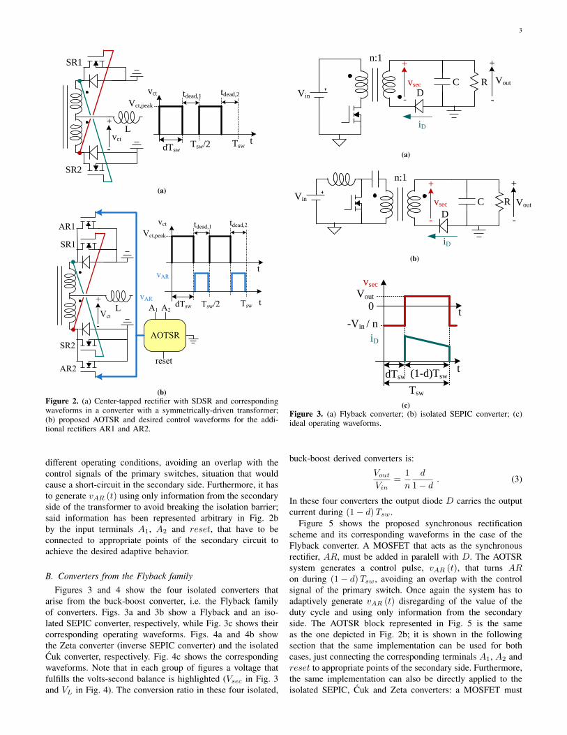
B. Converters from the Flyback family
Figures 3 and 4 show the four isolated converters thatarise from the buck-boost converter, i.e. the Flyback familyof converters. Figs. 3a and 3b show a Flyback and an iso-lated SEPIC converter, respectively, while Fig. 3c shows theircorresponding operating waveforms. Figs. 4a and 4b showthe Zeta converter (inverse SEPIC converter) and the isolatedCuk converter, respectively. Fig. 4c shows the correspondingwaveforms. Note that in each group of figures a voltage thatfulfills the volts-second balance is highlighted (Vsec in Fig. 3and VL in Fig. 4). The conversion ratio in these four isolated,
C RD
vsec
iD
n:1
Vin
Vout
-
+
-
+
(a)
C R
D
vsec
iD
n:1
Vin Vout
-
+
-
+
(b)
vsec
Tsw
0
t
Vout
-Vin / n
iD
t
dTsw (1-d)Tsw
(c)Figure 3. (a) Flyback converter; (b) isolated SEPIC converter; (c)ideal operating waveforms.
buck-boost derived converters is:
VoutVin
=1
n
d
1− d. (3)
In these four converters the output diode D carries the outputcurrent during (1− d)Tsw.
Figure 5 shows the proposed synchronous rectificationscheme and its corresponding waveforms in the case of theFlyback converter. A MOSFET that acts as the synchronousrectifier, AR, must be added in paralell with D. The AOTSRsystem generates a control pulse, vAR (t), that turns ARon during (1− d)Tsw, avoiding an overlap with the controlsignal of the primary switch. Once again the system has toadaptively generate vAR (t) disregarding of the value of theduty cycle and using only information from the secondaryside. The AOTSR block represented in Fig. 5 is the sameas the one depicted in Fig. 2b; it is shown in the followingsection that the same implementation can be used for bothcases, just connecting the corresponding terminals A1, A2 andreset to appropriate points of the secondary side. Furthermore,the same implementation can also be directly applied to theisolated SEPIC, Cuk and Zeta converters: a MOSFET must

4
C RD
vL
iD
n:1
Vin
-+
-
+
Vout
L
(a)
n:1
Vin C RD iD
-
+
Vout
-+vL
(b)
vL
Tsw
0
t
-Vout
Vin / n
iD
t
dTsw (1-d)Tsw
(c)Figure 4. (a) Isolated Zeta converter (inverse SEPIC); (b) isolatedCuk converter; (c) ideal operating waveforms.
C RD
vsec
Tsw
0
t
vsec
Vout
-Vin / n
iAR
t
iAR
dTsw (1-d)Tsw
AOTSR
A1 A2
reset
vARt
vARAR
n:1
-
+
-
+
Vout
Figure 5. Proposed AOTSR system and corresponding waveforms ina Flyback converter.
be placed in paralell with D and activated during (1− d)Tsw.Note that in these four converters the auxiliary synchronousrectifier is ground-referenced.
III. IMPLEMENTATION OF THE ADAPTIVE OFF-TIMESYNCHRONOUS RECTIFICATION
Fig. 6 shows the proposed implementation of the AOTSRsystem. It is comprised of a peak detector (Dpd and Cpd), twocurrent mirrors (one made up of T1 and T2, and the second
made up of T3 and T4) and a comparator. The key idea of thecircuit is to charge Cpd to the peak voltage between A1 andA2 in each switching cycle:
VCpd = max VA1 (t)− VA2 (t)Tsw≥t≥0 . (4)
Within a switching cycle, VCpd is assummed to remain con-stant. Cpd must be selected small enough to avoid any changein the operation of the converter, and at the same time it shouldbe able to maintain its voltage approximately constant duringa switching cycle, taking into account the current demandof the AOTSR circuitry. A capacitance in the range of afew hundreds of nanofarads is suitable for this application.Neglecting voltage drops in the transistor junctions, the currentgenerated by the first current mirror, T1 and T2, is:
IT1 = IT2 =VCpd
R1. (5)
IT1generates a voltage at the positive input of the comparator
equal to:
V+ = R2 ·VCpd
R1=R2
R1VCpd . (6)
Neglecting the voltage drop across Dpd, the current generatedby the second current mirror (T3 and T4) is:
IT3 = IT4 =VA1
Rramp, (7)
VA1 being the voltage at A1. Following Fig. 6, IT4 chargesCramp generating the following voltage waveform at thenegative input of the comparator:
V− (t) =VA1
RrampCrampt . (8)
The time when the voltage ramp V− equals V+ determines thelenght of the control pulse, tVAR. Using (6) and (8):
VA1
RrampCramptVAR =
R2
R1VCpd ⇒
⇒ tVAR = RrampCrampR2
R1
VCpd
VA1. (9)
Therefore, tVAR depends on the values of R1, R2, Cramp andRramp, as long as on the voltage at A1 and on the peak voltagebetween A1 and A2, i.e. the voltage VCpd.
From Figs. 2b and 5, it is apparent that the AOTSRmust ensure that vAR (t) goes to zero during the conductionintervals of the primary side transistors (during [0, dTsw]and [Tsw/2, Tsw/2 + dTsw] in converters with symmetrically-driven transformers and during [0, dTsw] in converters fromthe Flyback family), to avoid overlapping. This is achievedthrough the reset transistor Mreset: assumming that the resetterminal is connected to a voltage that goes high during theconduction intervals of the main transistors, both inputs ofthe comparator will be pulled low during such intervals. Notefrom Fig. 6 that the voltage at the negative input is slightlyhigher than the voltage at the positive input, due to the differentforward voltage drop of each diode: V− is pulled down tothe forward voltage drop of the PN diode Dreset−, which isslightly higher than the forward voltage drop of the Schottkydiode Dreset+, ensuring that vAR (t) is 0 whenever Mreset is

5
R1
R2
T1 T2 T3 T4
Rramp Cramp
-
+
vAR
Mreset
Dreset+
Dreset-
A1
A2
v-
v+
comparator
AOTSR system
Cpd
Dpd
reset
VCpd
+
-
+
-
VA1
Figure 6. Circuit implementation of the AOTSR system.
L
SR1
SR2
AR2
AR1
vAR
+
-
vct
AOTSR
A1 A2
reset
C R
+
-
Vout
Figure 7. Connection of the proposed AOTSR system in a converterwith a symmetrically-driven transformer.
activated. This reset mechanism guarantees that the proposedsystem causes no overlap, even in the presence of suddenchanges of the duty cycle. Several alternatives are possible toavoid DCM operation of the proposed AOTSR; for instance,if the current through the rectifier becomes negative and at thesame time VAR is high, then VAR can be immediately pulledlow. This can be done using very few additional components.
A. Converters with symmetrically-driven transformersFig. 7 shows the proposed system in the case of converters
with symmetrically driven transformers. A1 and A2 must be
connected to the center tap of the transformer and to the outputterminal, respectively. The reset terminal is also connectedto the center tap, thus reseting the AOTSR during the desiredintervals. With the aforementioned connections, VCpd and VA1
are:
VCpd= Vct,peak − Vout (10)VA1 = Vct,peak . (11)
Using (10), (11) and (1), (9) can be written as:
tVAR =R2
R1RrampCramp (1− 2d) . (12)
Now choosing R1, R2, Rramp and Cramp as:
RrampCrampR2
R1= k
Tsw2
, (13)
k being a safety factor to ensure that no short circuits takeplace, (9) can be written as:
tVAR = kTsw2
(1− 2d) . (14)
Comparing (14) with (2), it is apparent that, with the aforemen-tioned selection of the component values described by (13),the duration of the pulse can be made as close to the durationof the dead times as desired; in practice k will be chosen to bearound 0.9 to avoid overlapping and at the same time maximizetVAR. Furthermore, (14) yields the desired adaptive behavior:the higher the duty cycle, the shorter tVAR. Fig. 8 shows theoperating waveforms of the AOTSR for two different valuesof the duty cycle.
B. Converters from the Flyback family
Fig. 9 shows the proposed system in the case of a Flybackconverter. In this case, A1 and A2 must be connected tothe cathode of D and to the output, respectively. The resetterminal is also connected to the cathode of D, again pulling

6
Tsw/2 Tsw
tdead,1 tdead,2
0 t
vct dTsw dTsw
tVAR
vAR
V+V-
tVAR
t
t
(a)
Tsw/2 Tsw
tdead,1 tdead,2
0 t
vct dTsw dTsw
tVAR
vAR
V+V-
tVAR
t
t
(b)Figure 8. Operating waveforms of the AOTSR in a converter with asymmetrically driven transformer: (a) d ≈ 0.25; (b) d ≈ 0.15.
vAR (t) low during the desired intervals. With the aforemen-tioned connections, VCpd and VA1 are:
VCpd=Vinn
(15)
VA1 =Vinn
+ Vout . (16)
Using (15), (16) and (3), (9) can now be written as:
tVAR =R2
R1RrampCramp (1− d) . (17)
Now choosing R1, R2, Rramp and Cramp fulfilling:
R2
R1RrampCramp = kTsw , (18)
k being a safety factor to ensure that no short circuits takeplace, (9) can be written as:
tVAR = kTsw (1− d) . (19)
Once again, it is apparent that, with the aforementionedselection of the component values, the duration of the pulsecan be made as close to the duration of the diode conductiontime as desired; in practice k will be chosen to be around 0.9to avoid possible short circuits and at the same time maximizetVAR. Equation (19) again yields the desired adaptive behavior:the higher the duty cycle, the shorter tVAR. Fig. 10 shows theoperating waveforms of the AOTSR for two different valuesof the duty cycle.
Figure 9 is also applicable to the isolated SEPIC converter,whereas the appropriate connections in the case of the isolatedZeta and Cuk converters are shown in Fig. 11
C RD
vsec
AOTSR
A1A2
reset
vARAR
n:1
-
+
-
+
Vout
Figure 9. Connection of the proposed AOTSR system to a Flybackconverter.
Tsw 2Tsw
(1-d)Tsw
0 t
vsec dTsw dTsw
tVAR
vAR
V+V-
(1-d)Tsw
Vout
-Vin / n
(a)
Tsw 2Tsw
(1-d)Tsw
0 t
vsec dTsw
tVAR
vAR
V+V-
(1-d)TswdTsw
Vout
-Vin / n
tVAR
(b)Figure 10. Operating waveforms of the AOTSR in the Flybackconverter: (a) D ≈ 0.5; (b) D ≈ 0.3.
IV. EXPERIMENTAL RESULTS
Two converters were used to test the proposed system. A100 W Push-Pull converter was used to implement the AOTSRsystem in a converter with a symmetrically-driven transformer;a 50 W Flyback converter was selected to test the system inan isolated buck-boost derived topology. The results obtainedare shown in the following sections.

7
C RD
n:1
AR
AOTSR
A1 A2
reset
vAR
L
(a)
n:1
C RDAR
L
AOTSR
A1 A2
reset
vAR
(b)Figure 11. (a) AOTSR connections for an isolated Zeta converter;(b) AOTSR connections for an isolated Cuk converter.
A. 100 W Push-Pull converter
The main specifications of the Push-Pull converter are:Vin = 18 − 36 V , Vout = 3.3 − 5 V , L = 3.3 µHand C = 120 µF . The transformer has three primary turnsand one secondary turn in each winding, and the switchingfrequency is 115 kHz. IRL1404 MOSFETs are used as themain synchronous rectifiers SR1 and SR2; the same model isused for the auxiliar rectifiers AR1 and AR2. General purpose(but matched) transistors (BC557) are used as T1, T2, T3and T4 in the AOTSR system. A fast response comparator(AD790) is also used: this is a high performance, expensivecomparator, and much cheaper integrated circuits (as theTL3016 used in the following section) could be used. Theauxiliar rectifiers are driven by an additional MOSFET driver,UCC27424, supplied from an unregulated voltage obtainedfrom the transformer; according to the specifications of theconverter, the supply voltage changed from 6 V (Vin = 18 V )to 12 V (Vin = 36 V ). A higher drive voltage can be easilyobtained from one of the secondary windings, whose peakvoltage is equal to 2Vct, therefore providing a voltage rangingfrom 12 V to 24 V; a linear regulator is then required toavoid an excessive gate voltage. Table I summarizes the designof the AOTSR. To account for component tolerances, Rramp
has been replaced with a variable resistance to implement aconservative design (k < 0.8).
Fig. 12 shows the efficiency measured at different operat-ing conditions, with and without the proposed system: it isapparent that the AOTSR noticeably increases the efficiency
Table I. Design parameters of the AOTSR for the Push-Pull converter.Tsw
2k R1 R2 Rramp Cramp
(µs) (kΩ) (kΩ) (kΩ) (nF)
4.35 0.8 5 5 3.9 1
40 50 60 70 80 90 100 11080
82
84
86
88
90
92
Output power (W)
Eff
icie
ncy
(%
)
Vin
= 24 (SDSR)
Vin
= 24 (SDSR+AOTSR)
Vin
= 36 (SDSR)
Vin
= 36 (SDSR+AOTSR)
Output current (A)8 10 12 14 16 18 20 22
(a)
20 40 60 80 100 120
74
76
78
80
82
84
86
88
90
Output power (W)
Eff
icie
ncy
(%
)
Vin
=36 V (SDSR)
Vin
=36 V (SDSR+AOTSR)
Vin
=24 V (SDSR)
Vin
=24 V (SDSR+AOTSR)
Vin
=18 V (SDSR)
Vin
=18 V (SDSR+AOTSR)
6 9 12 15 18 21 24 27 30 33 36
Output current (A)
(b)Figure 12. Measured efficiency with and without the proposedsystem: (a) Vout = 5 V ; (b) Vout = 3.3 V .
regardless of the input and output voltages. The efficiencyincrease achieved is higher for Vin = 36 V , i.e. whenthe conduction time of the auxiliar rectifier is longer. Fig.13 shows several operating waveforms. It can be seen thatthe proposed system presents the expected adaptive behavior,changing tVAR according to (14).
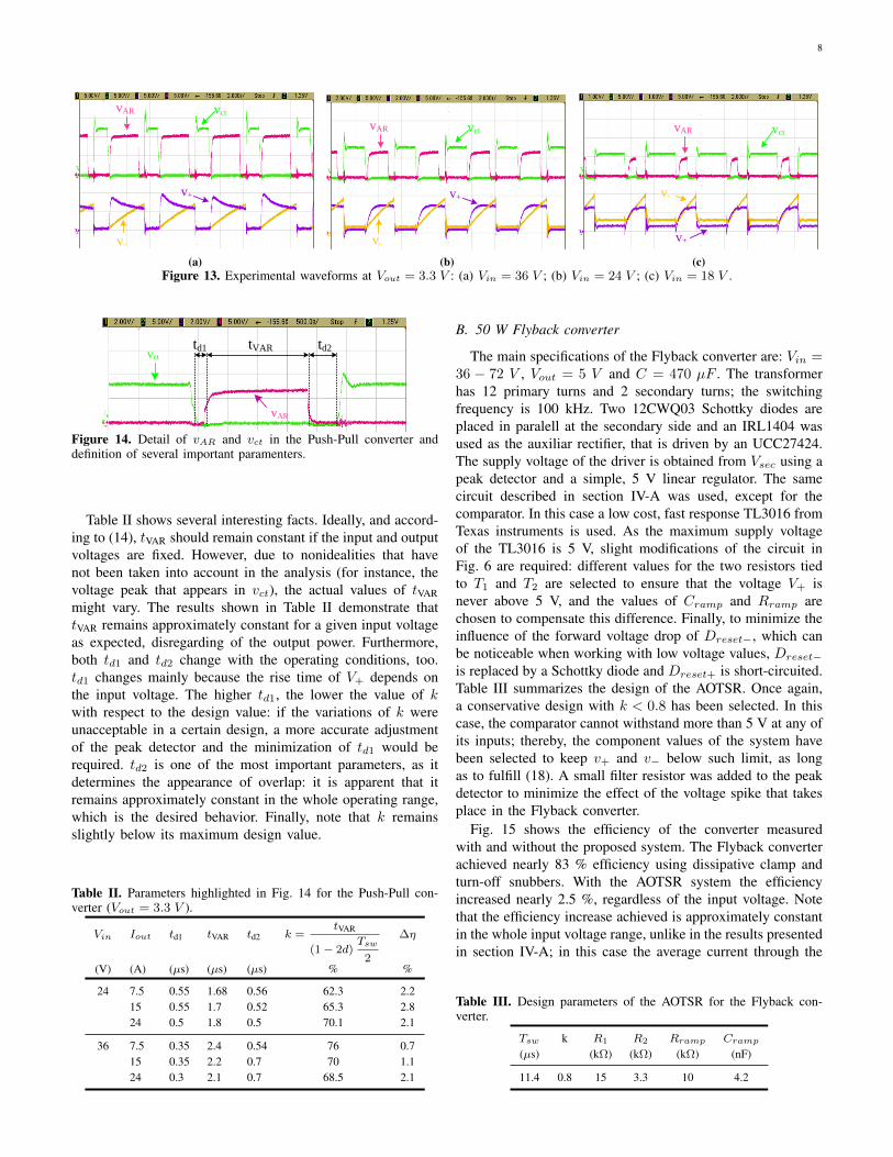
Figure 14 shows a sample operating waveform in detail,and Table II shows the values of the parameters highlightedin Fig. 14 for different operating conditions: td1 and td2 haveto be long enough to guarantee that no overlapping takes place,disregarding of the operating conditions. td1 is determined bythe rising time of V+ and by the delays introduced by the turn-off of Mreset, the comparator and the gate drive circuitry of theauxiliar rectifiers. The rising time of V+ is in turn determinedby R1 and the equivalent capacitance at the positive input ofthe comparator. As overlapping is less likely to take place atthe turn-on of the auxiliar rectifiers, the aforementioned delaysand the rising time of V+ should be minimized to maximizethe efficiency improvement. Interval td2 is determined by thevalue of k. The value of tVAR is also shown in Table II, alongwith its relative lenght with respect to the dead times and theefficiency improvement achieved (∆η).
8
vAR vct
v-
v+
(a)
vAR vct
v-
v+
(b)
vAR vct
v-
v+
(c)Figure 13. Experimental waveforms at Vout = 3.3 V : (a) Vin = 36 V ; (b) Vin = 24 V ; (c) Vin = 18 V .
vAR
vct
td1 td2tVAR
Figure 14. Detail of vAR and vct in the Push-Pull converter anddefinition of several important paramenters.
Table II shows several interesting facts. Ideally, and accord-ing to (14), tVAR should remain constant if the input and outputvoltages are fixed. However, due to nonidealities that havenot been taken into account in the analysis (for instance, thevoltage peak that appears in vct), the actual values of tVARmight vary. The results shown in Table II demonstrate thattVAR remains approximately constant for a given input voltageas expected, disregarding of the output power. Furthermore,both td1 and td2 change with the operating conditions, too.td1 changes mainly because the rise time of V+ depends onthe input voltage. The higher td1, the lower the value of kwith respect to the design value: if the variations of k wereunacceptable in a certain design, a more accurate adjustmentof the peak detector and the minimization of td1 would berequired. td2 is one of the most important parameters, as itdetermines the appearance of overlap: it is apparent that itremains approximately constant in the whole operating range,which is the desired behavior. Finally, note that k remainsslightly below its maximum design value.
Table II. Parameters highlighted in Fig. 14 for the Push-Pull con-verter (Vout = 3.3 V ).
Vin Iout td1 tVAR td2 k =tVAR
(1 − 2d)Tsw
2
∆η
(V) (A) (µs) (µs) (µs) % %
24 7.5 0.55 1.68 0.56 62.3 2.215 0.55 1.7 0.52 65.3 2.824 0.5 1.8 0.5 70.1 2.1
36 7.5 0.35 2.4 0.54 76 0.715 0.35 2.2 0.7 70 1.124 0.3 2.1 0.7 68.5 2.1
B. 50 W Flyback converter
The main specifications of the Flyback converter are: Vin =36 − 72 V , Vout = 5 V and C = 470 µF . The transformerhas 12 primary turns and 2 secondary turns; the switchingfrequency is 100 kHz. Two 12CWQ03 Schottky diodes areplaced in paralell at the secondary side and an IRL1404 wasused as the auxiliar rectifier, that is driven by an UCC27424.The supply voltage of the driver is obtained from Vsec using apeak detector and a simple, 5 V linear regulator. The samecircuit described in section IV-A was used, except for thecomparator. In this case a low cost, fast response TL3016 fromTexas instruments is used. As the maximum supply voltageof the TL3016 is 5 V, slight modifications of the circuit inFig. 6 are required: different values for the two resistors tiedto T1 and T2 are selected to ensure that the voltage V+ isnever above 5 V, and the values of Cramp and Rramp arechosen to compensate this difference. Finally, to minimize theinfluence of the forward voltage drop of Dreset−, which canbe noticeable when working with low voltage values, Dreset−is replaced by a Schottky diode and Dreset+ is short-circuited.Table III summarizes the design of the AOTSR. Once again,a conservative design with k < 0.8 has been selected. In thiscase, the comparator cannot withstand more than 5 V at any ofits inputs; thereby, the component values of the system havebeen selected to keep v+ and v− below such limit, as longas to fulfill (18). A small filter resistor was added to the peakdetector to minimize the effect of the voltage spike that takesplace in the Flyback converter.
Fig. 15 shows the efficiency of the converter measuredwith and without the proposed system. The Flyback converterachieved nearly 83 % efficiency using dissipative clamp andturn-off snubbers. With the AOTSR system the efficiencyincreased nearly 2.5 %, regardless of the input voltage. Notethat the efficiency increase achieved is approximately constantin the whole input voltage range, unlike in the results presentedin section IV-A; in this case the average current through the
Table III. Design parameters of the AOTSR for the Flyback con-verter.
Tsw k R1 R2 Rramp Cramp
(µs) (kΩ) (kΩ) (kΩ) (nF)
11.4 0.8 15 3.3 10 4.2

9
20 25 30 35 40 45 50 5578
79
80
81
82
83
84
85
86
87
Output power (W)
Eff
icie
ncy
(%
)
Vin = 72 V (diode)
Vin = 72 V (AOTSR)
Vin = 48 V (diode)
Vin = 48 V (AOTSR)
Vin = 36 V (diode)
Vin = 36 V (AOTSR)
4 5 6 7 8 9 10 11Output current (A)
Figure 15. Measured efficiency with and without the proposed systemat different operating conditions; the output voltage was Vout = 5 V .
VAR
td1 td2tVAR -Vsec
Figure 16. Detail of vAR and vsec in the Flyback converter anddefinition of several important parameters.
output diode only depends on the output power and doesnot change with the input voltage, causing the efficiencyincrease to remain approximately constant disregarding of theconduction time of the auxiliar rectifier.
Figure 16 shows a sample operating waveform in detail; thesame parameters shown in Table II have been measured in theFlyback converter and are shown in Table IV, and the sameconsiderations stated in Section IV-A over td1 and td2 can beapplied here.
Similar conclusions to those obtained in the previous sectioncan be stated according to the results shown in Table IV. Onceagain, variations of the actual values of tVAR are small enoughto be neglected for constant input and output voltages. td1varies due to the same reasons explained in the case of thePush-Pull converter. td2 remains approximately constant in thewhole operating range, ensuring that no overlap takes place.Finally, k remains slightly below its maximum design value,and changes according to the variations in td1.
V. CONCLUSIONS
A novel adaptive off-time synchronous rectification systemhas been presented in this paper. The system is especiallysuitable for isolated, low output voltage converters, as it usesonly information from the secondary side of the transformer;this facts allows complex and sometimes unreliable pulsetransmission systems required to transfer the control pulsesto the secondary side when synchronous rectification is im-plemented. The proposed adaptive synchronous rectificationsystem is applicable to converters with symmetrically-driven
Table IV. Parameters highlighted in Fig. 14 for the Flyback converter(Vout = 5 V ).
Vin Iout td1 tVAR td2 k =tVAR
(1 − d)Tsw∆η
(V) (A) (µs) (µs) (µs) % %
36 4 1 3.45 1.6 57.5 1.96 1 3.45 1.6 58.2 2.28 1 3.45 1.6 58.2 2.3810 0.9 3.5 1.65 59 2.2
48 4 0.64 4.9 1.5 71.6 2.36 0.6 4.85 1.45 71 2.278 0.56 4.85 1.4 71 2.510 0.52 4.9 1.4 71.6 2.7
72 4 0.35 6.3 1.5 - 3.16 0.3 6.25 1.55 78.3 2.198 0.4 6.1 1.45 76.4 2.1410 0.45 6 1.5 76 2.5
transformers (Half and Full-bridges and Push-Pull) and toconverters from the isolated buck-boost family (Flyback, iso-lated SEPIC, Cuk and ZETA). The proposed system is simple,inexpensive and can easily be implemented in an integratedcircuit. It has been demonstrated that the system is capable ofincreasing up to a 3 % the efficiency of a 100 W Push-Pullconverter with SDSR, and nearly 2.5 % the efficiency of a50 W Flyback converter with Schottky diodes. Furthermore,it can reliably work in a wide range of operating conditionsdue to its adaptive behavior.
REFERENCES
[1] C. Blake, D. Kinzer, P. Wood “Synchronous rectifiers versus Schottkydiodes: A comparison of the losses of a synchronous rectifier versus thelosses of a Schottky diode rectifier”. IEEE Applied Power ElectronicsConference, vol. 1, pp. 17-23, 1994.
[2] J. A. Cobos, J. Uceda, “Low ouput voltage DC/DC conversion”. IndustrialElectronics, Control and Instrumentation Conference (IECON), vol. 3, pp.1676-1681, September 1994.
[3] H. Chiu and L. Lin. “A High-Efficiency Soft-Switched AC/DC ConverterWith Current-Doubler Synchronous Rectification”.IEEE Transactions onIndustrial Electronics, vol. 52, no. 3, pp. 709-718, June 2005.
[4] J. Blanc, “Practical application of MOSFET synchronous rectifiers”.International Telecommunications Energy Conference (INTELEC), pp.495-501, November 1991.
[5] J.A. Cobos, O. Garcıa, J. Sebastian, J. Uceda, “Active clamp PWMforward converter with self driven synchronous rectification”. Telecommu-nications Energy Conference (INTELEC), vol. 2, pp. 200-206, September1993.
[6] M. Jovanovic, M. T. Zhang, F. C. Lee, “Evaluation of Synchronous-Rectification Efficiency Improvement Limits in Forward Converters”.IEEE Transactions on Industrial Electronics, vol. 42, no. 4, pp. 387-395,August 1995.
[7] X. Xie, J. C. Liu, F. Poon and M. H. Pong. “A novel high frequencycurrent-driven synchronous rectifier applicable to most switching topolo-gies”. IEEE Transactions on Power Electronics, vol. 16, no. 5, pp. 635-648, September 2001.
[8] A. Fernandez, J. Sebastian, P. J. Villegas, M. M. Hernando and L. Alvarez.“Low-power Flyback converter with synchronous rectification for asystem with AC power distribution”. IEEE Transactions on IndustrialElectronics, vol. 49, no. 3, pp. 598-606, June 2002.
[9] J. Zhou, M. Xu, J. Sun and F. C. Lee. “A self-driven soft-switchingvoltage regulator for future microprocessors”. IEEE Transactions onPower Electronics, vol. 20, no. 4, pp. 806-814, July 2005.
[10] M. Xu, Y. Ren, J. Zhou and F. C. Lee. “1-MHz self-driven ZVS Full-bridge converter for 48-V Power Pod and DC/DC brick”. IEEE Trans-actions on Power Electronics, vol. 20, no. 5, pp. 997-1006, September2005.

10
v+
vAR -vsec
v-
(a)
v+
vAR
v-
-vsec
(b)
v+
vAR
v-
-vsec
(c)Figure 17. Experimental waveforms at Vout = 5 V . Vt refers to the : (a) Vin = 72 V ; (b) Vin = 48 V ; (c) Vin = 36 V .
[11] Y. Ren, M. Xu, J. Sun and F. C. Lee. “A family of high power densityunregulated bus converters”. IEEE Transactions on Power Electronics,vol. 20, no. 5, pp. 1045-1054, September 2005.
[12] D. Fu, F. C. Lee and M. Xu. “A novel driving scheme for synchronousrectifiers in LLC resonant converters”. IEEE Transactions on PowerElectronics, vol. 24, no. 5, pp. 1321-1329, May 2009.
[13] K. Jin, Y. Sun, M. Xu, D. Sterk and F. C. Lee. “Integrated magneticself-driven ZVS nonisolated Full-Bridge converter”. IEEE Transactionson Industrial Electronics, vol. 57, no. 5, pp. 1615-1623, May 2010.
[14] http://www.power-one.com/resources/products/datasheet/asq24 family v7.pdf.
[15] P. Alou, J. A. Cobos, O. Garcıa, R. Prieto, J. Uceda, “A new drivingscheme for synchronous rectifiers: single winding self-driven synchronousrectification”. IEEE Transactions on Power Electronics, vol. 16, issue 6,pp. 803-811, November 2001.
[16] A. Fernandez, J. Sebastian, M. M. Hernando, P. J. Villegas, J. Garcıa,“New self-driven synchronous rectification system for converters witha symmetrically driven transformer”. IEEE Transactions on IndustryApplications, vol. 41, issue 5, pp. 1307-1315, September-October 2005.
[17] A. Fernandez, D. G. Lamar, M. Rodrıguez, M. M. Hernando, J. Sebastianand M. Arias. “Self-Driven synchronous rectification system with inputvoltage tracking for converters with a symmetrically driven transformer”.IEEE Transactions on Industrial Electronics, vol. 56, no. 5, pp. 1440-1445, May 2009.
[18] J. Lee, J. Kwon, E. Kim, W. Choi, B. Kwon. “Single-stage single-switchPFC Flyback converter using a Synchronous rectifier”. IEEE Transactionson Industrial Electronics, vol. 55, no. 3, pp. 1352-1365, March 2008.
Miguel Rodrıguez (S’06) was born in Gijon, Spain,in 1982. He received the M.S. degree in Telecommu-nication Engineering from the University of Oviedo,Spain, in 2006. Currently he is working towardsthe Ph.D. degree in the Department of Electricaland Electronic Engineering, also at the University ofOviedo, (granted by the Spanish Ministry of Scienceand Innovation under the FPU program).
His research interests include DC / DC conversionand power supply systems for RF amplifiers.
Diego G. Lamar Diego G. Lamar (M05) was bornin Zaragoza, Spain, in 1974. He received the M.Sc.degree, and the Ph.D. degree in Electrical Engineer-ing from the Universidad de Oviedo, Spain, in 2003and 2008, respectively.
In 2003 he became a Research Engineer at theUniversity of Oviedo and since September 2005, hehas been an Assistant Professor. His research inter-ests are switching-mode power supplies, convertermodelling and power-factor-correction converters.
He cooperates regularly with the IEEE and theIEEE–PELS Spanish Chapter.
Manuel Arias Manuel Arias Prez de Azpeitia (s05M’10) was born in Oviedo, Spain, in 1980. Hereceived the M. Sc. degree in electrical engineeringfrom the University of Oviedo, Gijn, Spain in 2005and the Ph. D. degree in the same university in2010.
Since February 2005, he has been a Researcherin the Deparment of Electrical and Electronic Engi-neering, University of Oviedo, developing electronicsystems for UPSs and electronic switching powersupplies. Since February 2007, he has also been an
Assistant Professor of electronics in the same University. His research interestsinclude dc-dc converters, dc-ac converters, UPSs and LED lighting.
Roberto Prieto Roberto Prieto (M99) received theM.Sc. and Ph.D. degree in electronic engineeringfrom the Technical University of Madrid, Spain, in1993 and 1998 respectively. Since 1994, he has beenan Assistant Professor at the Technical University ofMadrid, where he is currently Associate Professor.He has published more than 150 papers in Interna-tional conferences and journals, most of them fromthe IEEE. He is also a co-author of two internationalpatents and a technical advisor for several IEEEconferences and journals. He has been the advisor
on more than 20 masters theses and 5 doctoral theses and has participatedin more than 50 research projects as a research engineer. His main researchinterest is the design and modeling of magnetic components.
Javier Sebastian Javier Sebastin (M87) was bornin Madrid, Spain, in 1958. He received the M.Sc.degree from the Polytechnic University of Madrid,and the Ph.D. degree from the University of Oviedo,Spain, in 1981 and 1985, respectively. He was anAssistant Professor and an Associate Professor atboth the Polytechnic University of Madrid and atthe University of Oviedo, in Spain. Since 1992, hehas been with the University of Oviedo, where heis currently a Professor. His research interests areswitching-mode power supplies, modelling of dc-to-
dc converters, low output voltage dc-to-dc converters and high power factorrectifiers.


