Embed Size (px)
Citation preview
4.6.7. Wide-band LNAs, “noise signal feedback” and “noise cancellation” Another approach to the LNAs different from the conventional amplifiers
tuned to a certain frequency at the output, is to design a wide-band amplifier and to define the operating frequency at the input with a suitable passive band-pass filter or directly using the tuned behavior of the antenna. With this approach it is possible to use a wide-band amplifier for any frequency, certainly in the band of the amplifier, only by changing the input filter or the antenna. Another advantage of this approach is reduced neighboring channel interferance.
From the basic noise theory (4.6.3.1) it is known that the thermal noise generated in a resitor can be characterized with its r.m.s. voltage or current as
These are the r.m.s. values of the noise voltage or the noise current that are randomly varying “noise signals”. Similarly, the r.m.s. channel noise current generated in the inversion channel resistance of a MOS transistor is It can be theoretically shown that the channel resistace for a non velocity saturated transistor is equal to and hence the mean square channel noise current becomes
But it has been experimentally deduced that it is more realistic to write the expression as (4.153) where γ is a parameter1. The numerical value of γ usually varies from 0.5 to 0.8, and it is at the high end of this interval for velocity saturated transistors. It must not be overlooked that the noise voltages and currents of the resistors and transistors in a circuit are processed (amplified, fed-back, mixed, etc.) as other signals in the circuit, until they reach the output circuit. Then their contribution to the total noise power at the output must be calculated and added-on to find the total noise power. The r.m.s. values are necessary at this stage. However, calculating the noise r.m.s values in advance will mask some important effects; such as “noise feedback” that has been known since the early days of electronics2 , and the “noise cancellation” techniques that appeared in several recent publications. This fact will be exemplified on several basic circuits below.
1 A.J. Scholten et al. “Accurate Thermal Noise Model for Deep-Submicron CMOS”, IEDM 1999. 2 For example: H.J. Reich, “ Theory and Applications of Electron Tubes”, p. 201, McGraw-Hill, 1944.
4.4.7.1. The common gate amplifier as a wide-band LNA
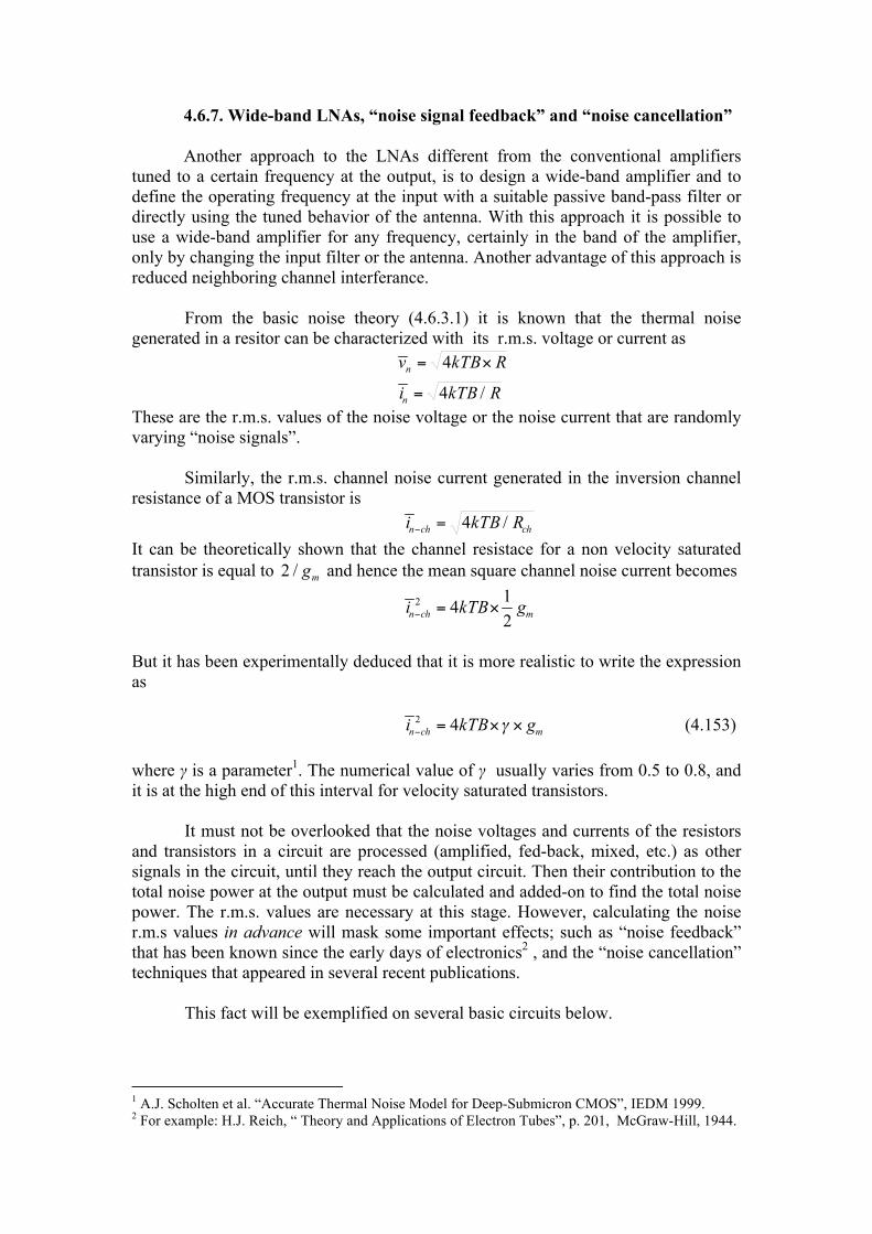
In a common gate amplifier given in Fig.4.59, there are three noisy components; the internal resistance of the input signal source, RA, the MOS transistor and the load resistor, RL. .
Figure 4.59 . The principal circuit diagram of a common gate amplifier
The contributions of these noise components to the output noise are as follows: a) Contribution of RA: The instantaneous value of the noise voltage of the source resistance is transferred to the input of the amplifier as
and then amplified by the transistor with a voltage gain of . Provided that the amplifier can be considered as linear for this signal level, the amplified noise voltage at the output is a replica of the noise voltage at the input and the r.m.s value of this voltage is equal to
(4.154)
and if the input is matched, i.e.
(4.154-a)
Since for a common gate amplifier,
(4.154-b)
Hence the noise power dissipated on the load resistance owing to the noise of the source resistance becomes
(4.155)
b) Contribution of the channel noise: The channel noise current of the
transistor flows through the load resistor RL as well as the internal resistance of the input signal source, RA. The noise current flowing through RA produces a voltage drop vni which provokes a channel noise current equal to
. This “feedback noise component” is in opposite direction with in-ch and
RL
RA
vA
ri
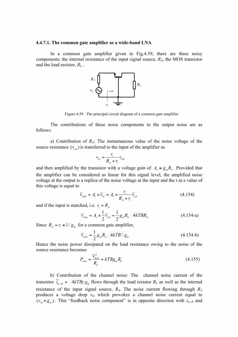
therefore reduces it. This qualitative explanation can be developed with the inclusion of the effect of the internal resistance of the transistor as shown in the equivalent circuit in Fig. 4.60(b) from which the resulting output noise current can be calculated as
, (a) (b) Figure 4.60(a). The channel noise current, (b) the equivalent circuit to calculate the internal feedback effect of this current.
(4.156)
where δ is the noise reduction parameter that approaches to ½ for The r.m.s. value of this noise current
(4.156-a) The contribution of the channel noise on the output power now can be calculated as (4.156-b) c) The contribution of the load resistance noise on the total output noise is simply (4.157)
Now the noise factor of a common gate amplifier can be written as
(4.158)
As an example for RA = 50 ohm, gm = 20 mS, RL = 500 ohm, rds = 1 kohm and
γ = 0.7 the noise factor is F = 1.83 that corresponds to a noise figure of NF = 2.6 dB
RL RA
in-ch
v ni
+
ri
RL RA vgs
in-ch
rds
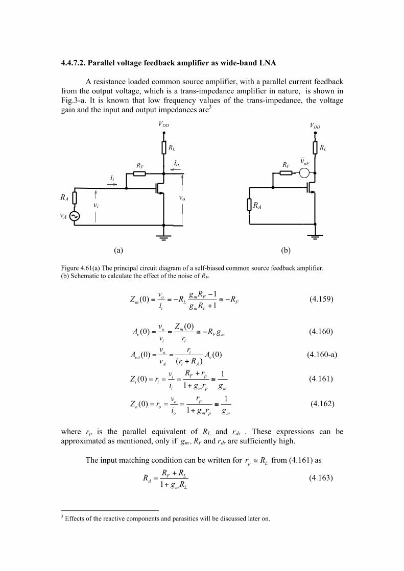
4.4.7.2. Parallel voltage feedback amplifier as wide-band LNA A resistance loaded common source amplifier, with a parallel current feedback from the output voltage, which is a trans-impedance amplifier in nature, is shown in Fig.3-a. It is known that low frequency values of the trans-impedance, the voltage gain and the input and output impedances are3 (a) (b) Figure 4.61(a) The principal circuit diagram of a self-biased common source feedback amplifier. (b) Schematic to calculate the effect of the noise of RF.
(4.159)
(4.160)
(4.160-a)
(4.161)
(4.162)
where rp is the parallel equivalent of RL and rds . These expressions can be approximated as mentioned, only if gm , RF and rds are sufficiently high.
The input matching condition can be written for from (4.161) as
(4.163)
3 Effects of the reactive components and parasitics will be discussed later on.
RF
RL
RA
VDD
RF
RL
VDD
RA
vA
vi
ii
vo
io
and with (4.163) , (4.159) and (4.160) can be arranged as (4.164)
(4.165)
---------------------------------- Problem 4.11. Derive expression (4.164).
---------------------------------- The noisy components in this circuit are the internal resistance of the input
signal source, RA, the MOS transistor, the load resistor, RL. and the feedback resistor, RF.
The contributions of these noise components to the output noise are as follows:
a) The equivalent noise voltage of the signal source internal resistance, is
transferred to the input of the amplifier as
(4.166)
where ri is the input resistance of the amplifier. Provided that the input is matched (i.e. RA = ri , the resulting output noise voltage signal
its RMS value
(4.167)
and the corresponding noise power at the output
Since
(4.168)
b) The output noise power component related to the channel noise current of the transistor is (4.169) c) The noise power of the load resistor RL itself is simply (4.170)
d) The contribution of RF on the output noise is two-fold; owing to the noise of itself and the negative feedback effect over RF.
Noise of RF is represented with a noise voltage source, in Fig. 4.61(b). This
source provokes a noise current along RL , RF and RA:
(4.171)
where .
The contribution of this current on the output noise power can be calculated as
(4.172)
Hence the total noise power dissipating on the load resistor owing to the noisy components of the amplifier becomes
(4.173)
that corresponds to an RMS output noise voltage of (4.174)
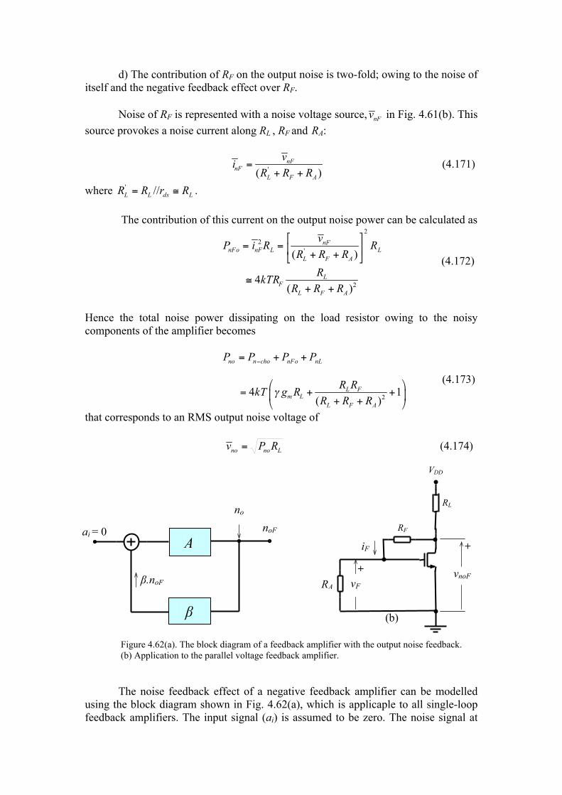
Figure 4.62(a). The block diagram of a feedback amplifier with the output noise feedback. (b) Application to the parallel voltage feedback amplifier. The noise feedback effect of a negative feedback amplifier can be modelled
using the block diagram shown in Fig. 4.62(a), which is applicaple to all single-loop feedback amplifiers. The input signal (ai) is assumed to be zero. The noise signal at
(b) (a)
RF
RL
VDD
RA vnoF
iF
vF
+
+
noF
A
β
β.noF
no
ai = 0
the output node of the amplifier originating from the components of the amplifier is shown as no. The total noise output signal noF is the sum of no and the feed-back noise signal:
that yields
This expression shows that if either β or A is negative (i.e. the feedback is negative) the noise signal at the output node becomes times smaller than the original noise.
For the amplifier shown in Fig. 4.62(b) the voltage feedback factor and the voltage gain are
(4.175)
(4.176)
(4.177)
where δ is the output noise voltage reduction factor owing to the feedback and is always smaller than unity. The corresponding noise power reduction factor is δ2 . Hence the output noise power and the noise factor with feedback become
(4.178)
(4.179)
Note that the noise factor increases with gm, strongly increases with RL and decreases with gain.
Now a design flow for an input matched self biasing parallel voltage feedback amplifier can be defined using (4.164), (4.165) and the D.C. operating conditions of the transistor:
The basic D.C. condition for the circuit is (4.180)

The drain current for a non-velocity saturated transistor
(4.181)
and for a velocity saturated transistor (4.182) Since the amplifier to be designed is a wide-band circuit, a velocity-saturated (small geometry) transistor must be preferred to extend the cut-off frequency. Therefore the design flow must be based on (4.164). These expressions lead to (4.183)
(4.184)
and (4.185)
(4.183) directly gives the value of RF corresponding to any source resistance and gain. (4.184) and (4.185) help to calculate the transconductance and the drain D.C. current corresponding to any anticipated load resistor that determines the -3dB frequency together with the load capacitance and the output node parasitics.
On the other hand, from (4.179) it can be seen that the noise factor increases linearly with gm, quadratically with RL and decreases quadratically with Av . Moreover, the power consumption linearly decreases with the increase of the load resistor. The bandwidth depends on the load resistance and the transistor geometry that affects the corner frequencies of the output as well as the input node. Therefore, there is a trade-off among noise, power consumption and bandwidth.
Example 4.11.
An input matched wide band LNA as shown in Fig. (4.61-a) will be designed.
0.18 micron UMC CMOS technology will be used where L =0.18 µm, VT = 0.3V, Cox = 8.2×10⁻⁷ F/cm2 and VDD = 2V. The internal resistance of the input signal source is RA = 50 ohm and the load capacitance is 100 fF. The required voltage gain from the source is 10 dB ( ), which corresponds to a voltage gain from the input node
of 16 dB ( ). The -3dB frequency and the noise figure at 1 GHz must be higher then 3 GHz and 3 dB, respectively. It will be assumed that the transistor is operating in the velocity saturated mode, that must be checked at the end of the design. The rds of the transistor will be assumed considerably higher than the drain load resistance.
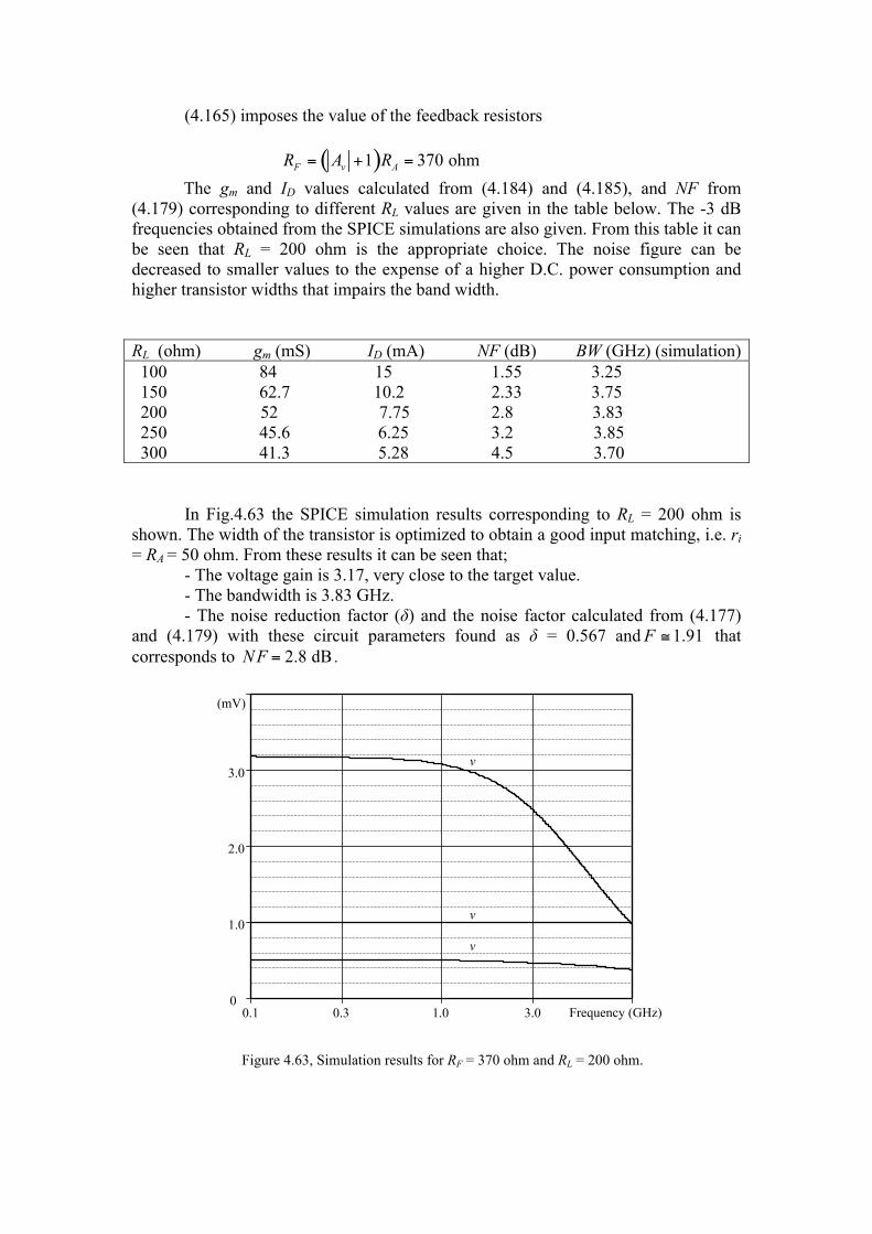
(4.165) imposes the value of the feedback resistors
The gm and ID values calculated from (4.184) and (4.185), and NF from (4.179) corresponding to different RL values are given in the table below. The -3 dB frequencies obtained from the SPICE simulations are also given. From this table it can be seen that RL = 200 ohm is the appropriate choice. The noise figure can be decreased to smaller values to the expense of a higher D.C. power consumption and higher transistor widths that impairs the band width.
RL (ohm) gm (mS) ID (mA) NF (dB) BW (GHz) (simulation) 100 84 15 1.55 3.25 150 62.7 10.2 2.33 3.75 200 52 7.75 2.8 3.83 250 45.6 6.25 3.2 3.85 300 41.3 5.28 4.5 3.70
In Fig.4.63 the SPICE simulation results corresponding to RL = 200 ohm is
shown. The width of the transistor is optimized to obtain a good input matching, i.e. ri = RA = 50 ohm. From these results it can be seen that;
- The voltage gain is 3.17, very close to the target value. - The bandwidth is 3.83 GHz.
- The noise reduction factor (δ) and the noise factor calculated from (4.177) and (4.179) with these circuit parameters found as δ = 0.567 and that corresponds to .
Figure 4.63, Simulation results for RF = 370 ohm and RL = 200 ohm.
Frequency (GHz) 0.1 0.3 1.0 3.0 0
1.0
2.0
3.0
4.0mV
(mV)
vo
vA vi
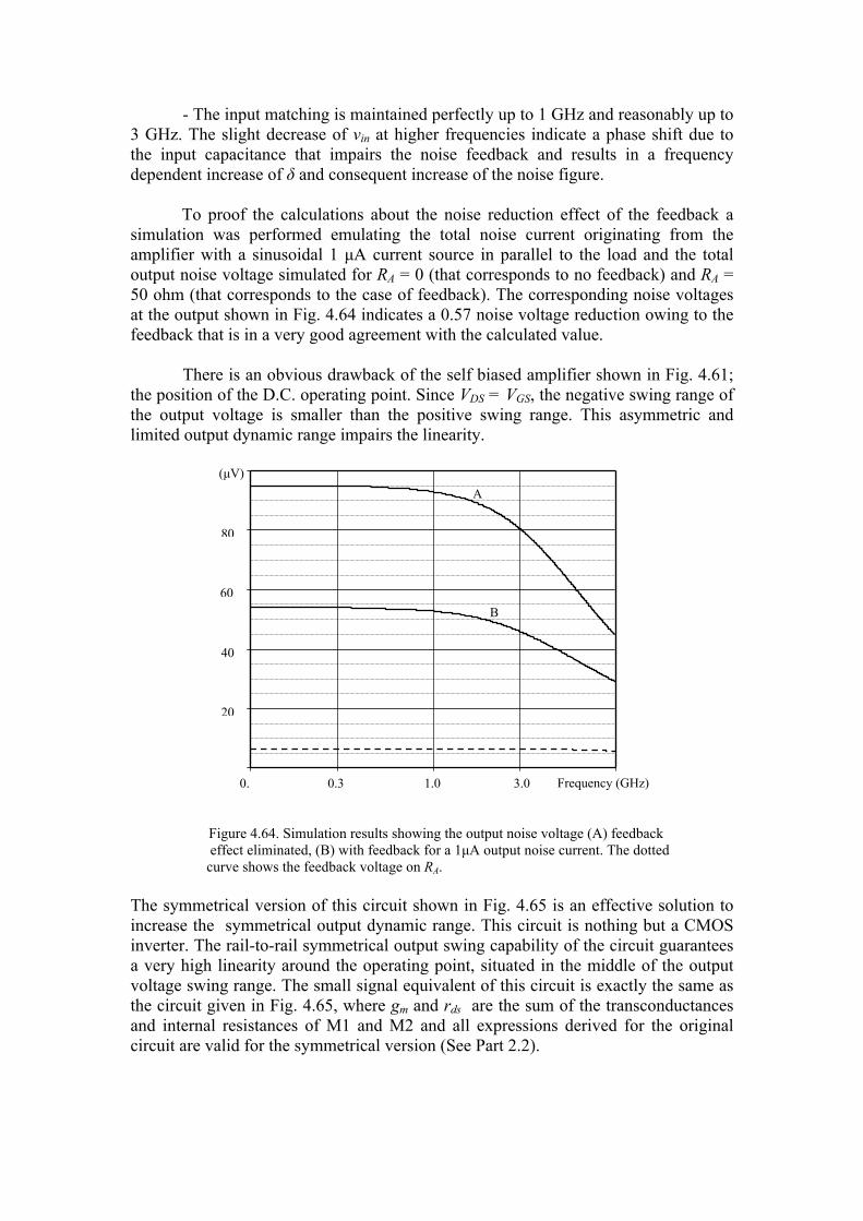
- The input matching is maintained perfectly up to 1 GHz and reasonably up to 3 GHz. The slight decrease of vin at higher frequencies indicate a phase shift due to the input capacitance that impairs the noise feedback and results in a frequency dependent increase of δ and consequent increase of the noise figure. To proof the calculations about the noise reduction effect of the feedback a simulation was performed emulating the total noise current originating from the amplifier with a sinusoidal 1 µA current source in parallel to the load and the total output noise voltage simulated for RA = 0 (that corresponds to no feedback) and RA = 50 ohm (that corresponds to the case of feedback). The corresponding noise voltages at the output shown in Fig. 4.64 indicates a 0.57 noise voltage reduction owing to the feedback that is in a very good agreement with the calculated value.
There is an obvious drawback of the self biased amplifier shown in Fig. 4.61; the position of the D.C. operating point. Since VDS = VGS, the negative swing range of the output voltage is smaller than the positive swing range. This asymmetric and limited output dynamic range impairs the linearity.
Figure 4.64. Simulation results showing the output noise voltage (A) feedback effect eliminated, (B) with feedback for a 1µA output noise current. The dotted curve shows the feedback voltage on RA. The symmetrical version of this circuit shown in Fig. 4.65 is an effective solution to increase the symmetrical output dynamic range. This circuit is nothing but a CMOS inverter. The rail-to-rail symmetrical output swing capability of the circuit guarantees a very high linearity around the operating point, situated in the middle of the output voltage swing range. The small signal equivalent of this circuit is exactly the same as the circuit given in Fig. 4.65, where gm and rds are the sum of the transconductances and internal resistances of M1 and M2 and all expressions derived for the original circuit are valid for the symmetrical version (See Part 2.2).
20
40
60
100uV
Frequency (GHz) 0.1
0.3 1.0 3.0
A
B
80
(µV)
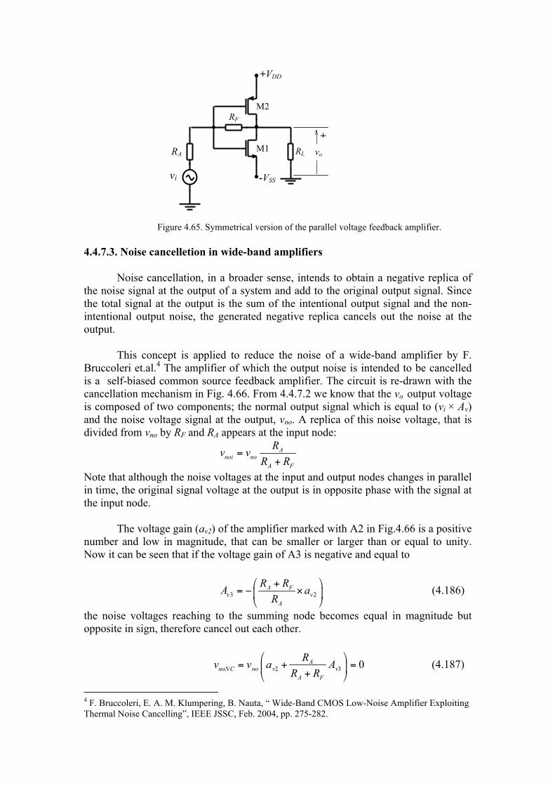
Figure 4.65. Symmetrical version of the parallel voltage feedback amplifier. 4.4.7.3. Noise cancelletion in wide-band amplifiers
Noise cancellation, in a broader sense, intends to obtain a negative replica of the noise signal at the output of a system and add to the original output signal. Since the total signal at the output is the sum of the intentional output signal and the non-intentional output noise, the generated negative replica cancels out the noise at the output.
This concept is applied to reduce the noise of a wide-band amplifier by F.
Bruccoleri et.al.4 The amplifier of which the output noise is intended to be cancelled is a self-biased common source feedback amplifier. The circuit is re-drawn with the cancellation mechanism in Fig. 4.66. From 4.4.7.2 we know that the vo output voltage is composed of two components; the normal output signal which is equal to (vi × Av) and the noise voltage signal at the output, vno. A replica of this noise voltage, that is divided from vno by RF and RA appears at the input node:
Note that although the noise voltages at the input and output nodes changes in parallel in time, the original signal voltage at the output is in opposite phase with the signal at the input node. The voltage gain (av2) of the amplifier marked with A2 in Fig.4.66 is a positive number and low in magnitude, that can be smaller or larger than or equal to unity. Now it can be seen that if the voltage gain of A3 is negative and equal to
(4.186)
the noise voltages reaching to the summing node becomes equal in magnitude but opposite in sign, therefore cancel out each other.
(4.187)
4 F. Bruccoleri, E. A. M. Klumpering, B. Nauta, “ Wide-Band CMOS Low-Noise Amplifier Exploiting Thermal Noise Cancelling”, IEEE JSSC, Feb. 2004, pp. 275-282.
+VDD
M1
M2
RL
RF
vi
RA
-VSS
vo
+
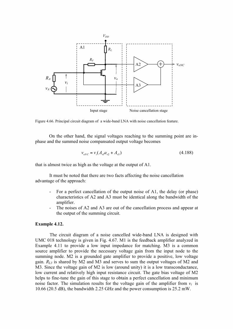
Figure 4.66. Principal circuit diagram of a wide-band LNA with noise cancellation feature. On the other hand, the signal voltages reaching to the summing point are in-phase and the summed noise compansated output voltage becomes (4.188) that is almost twice as high as the voltage at the output of A1. It must be noted that there are two facts affecting the noise cancellation advantage of the approach:
- For a perfect cancellation of the output noise of A1, the delay (or phase) characteristics of A2 and A3 must be identical along the bandwidth of the amplifier.
- The noises of A2 and A3 are out of the cancellation process and appear at the output of the summing circuit.
Example 4.12. The circuit diagram of a noise cancelled wide-band LNA is designed with UMC 018 technology is given in Fig. 4.67. M1 is the feedback amplifier analyzed in Example 4.11 to provide a low input impedance for matching. M3 is a common source amplifier to provide the necessary voltage gain from the input node to the summing node. M2 is a grounded gate amplifier to provide a positive, low voltage gain. RL3 is shared by M2 and M3 and serves to sum the output voltages of M2 and M3. Since the voltage gain of M2 is low (around unity) it is a low transconductance, low current and relatively high input resistance circuit. The gate bias voltage of M2 helps to fine-tune the gain of this stage to obtain a perfect cancellation and minimum noise factor. The simulation results for the voltage gain of the amplifier from vi is 10.66 (20.5 dB), the bandwidth 2.25 GHz and the power consumption is 25.2 mW.
VDD
RF
RL
RA
vA
vi
A2
vo
A3
voNC
A1
Input stage Noise cancellation stage
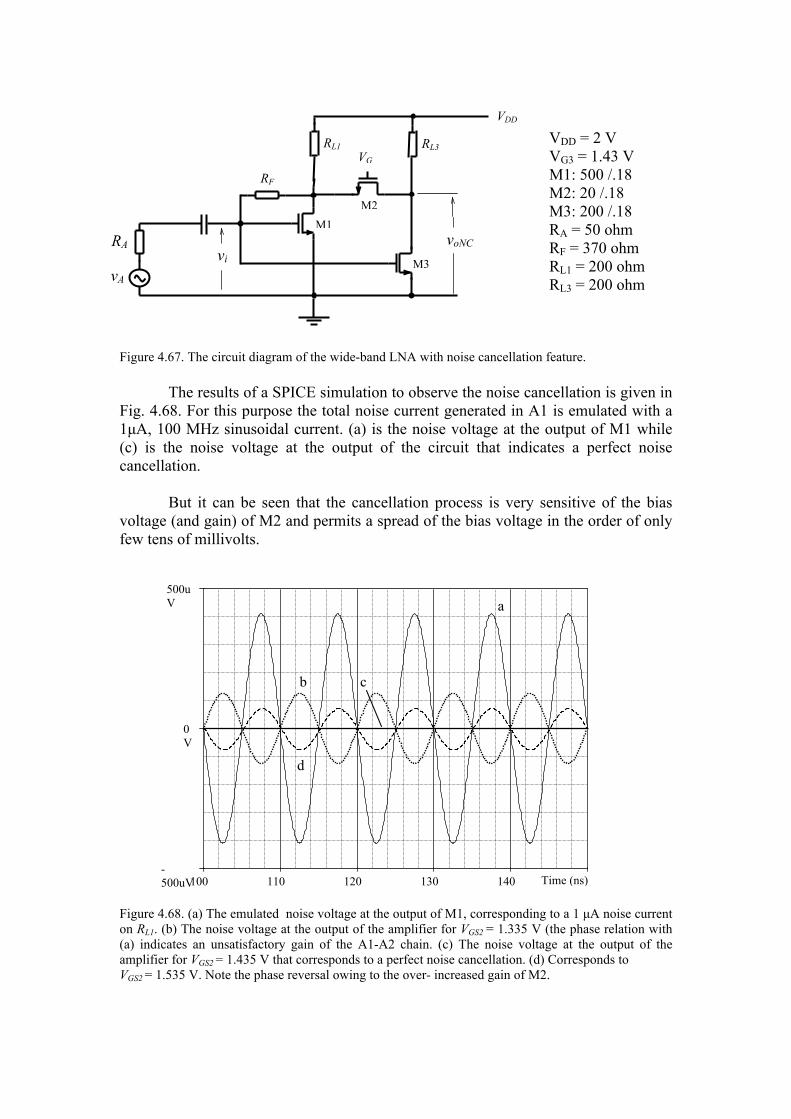
Figure 4.67. The circuit diagram of the wide-band LNA with noise cancellation feature. The results of a SPICE simulation to observe the noise cancellation is given in Fig. 4.68. For this purpose the total noise current generated in A1 is emulated with a 1µA, 100 MHz sinusoidal current. (a) is the noise voltage at the output of M1 while (c) is the noise voltage at the output of the circuit that indicates a perfect noise cancellation. But it can be seen that the cancellation process is very sensitive of the bias voltage (and gain) of M2 and permits a spread of the bias voltage in the order of only few tens of millivolts. Figure 4.68. (a) The emulated noise voltage at the output of M1, corresponding to a 1 µA noise current on RL1. (b) The noise voltage at the output of the amplifier for VGS2 = 1.335 V (the phase relation with (a) indicates an unsatisfactory gain of the A1-A2 chain. (c) The noise voltage at the output of the amplifier for VGS2 = 1.435 V that corresponds to a perfect noise cancellation. (d) Corresponds to VGS2 = 1.535 V. Note the phase reversal owing to the over- increased gain of M2.
VDD
RF
RL1
RA
vA
vi
voNC
M1
RL3
M2
M3
VG
2
VDD = 2 V VG3 = 1.43 V M1: 500 /.18 M2: 20 /.18 M3: 200 /.18 RA = 50 ohm RF = 370 ohm RL1 = 200 ohm RL3 = 200 ohm
Time (ns) 100 110 120 130 140 -500uV
0V
500uV a
b c
d
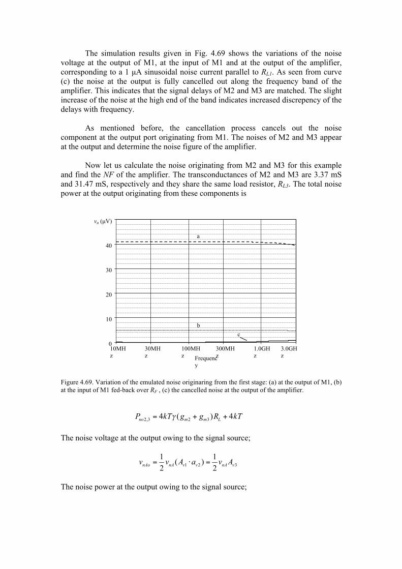
The simulation results given in Fig. 4.69 shows the variations of the noise voltage at the output of M1, at the input of M1 and at the output of the amplifier, corresponding to a 1 µA sinusoidal noise current parallel to RL1. As seen from curve (c) the noise at the output is fully cancelled out along the frequency band of the amplifier. This indicates that the signal delays of M2 and M3 are matched. The slight increase of the noise at the high end of the band indicates increased discrepency of the delays with frequency. As mentioned before, the cancellation process cancels out the noise component at the output port originating from M1. The noises of M2 and M3 appear at the output and determine the noise figure of the amplifier. Now let us calculate the noise originating from M2 and M3 for this example and find the NF of the amplifier. The transconductances of M2 and M3 are 3.37 mS and 31.47 mS, respectively and they share the same load resistor, RL3. The total noise power at the output originating from these components is
Figure 4.69. Variation of the emulated noise originaring from the first stage: (a) at the output of M1, (b) at the input of M1 fed-back over RF , (c) the cancelled noise at the output of the amplifier. The noise voltage at the output owing to the signal source;
The noise power at the output owing to the signal source;
Frequency
10MHz
30MHz
100MHz
300MHz
1.0GHz
3.0GHz
0
10
20
30
40
vn (µV)
a
b c
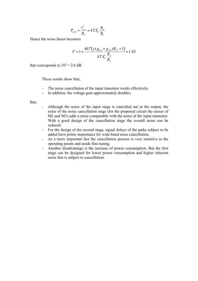
Hence the noise factor becomes
that corresponds to NF = 2.6 dB.
These results show that;
- The noise cancellation of the input transistor works effectively. - In addition, the voltage gain approximately doubles.
But; - Although the noise of the input stage is cancelled out at the output, the
noise of the noise cancellation stage (for the proposed circuit the noises of M2 and M3) adds a noise comparable with the noise of the input transistor. With a good design of the cancellation stage the overall noise can be reduced.
- For the design of the second stage, signal delays of the paths subject to be added have prime importance for wide-band noise cancellation.
- As a more important fact the cancellation process is very sensitive to the operating points and needs fine-tuning.
- Another disadvantage is the increase of power consumption. But the first stage can be designed for lower power consumption and higher inherent noise that is subject to cancellation.


