Embed Size (px)
Citation preview

3D Printed Horn Antenna for UltraWideband Applications
By Vegard Midtbøen
Thesis submitted for the degree of
Master of science in Electronics and computer
science, Microelectronics
60 credits
Department of Informatics
Faculty of mathematics and natural sciences
UNIVERSITY OF OSLO
Spring 2017


3D Printed Horn Antenna for
Ultra Wideband Applications
By Vegard Midtbøen

© 2017 By Vegard Midtbøen
3D Printed Horn Antenna for Ultra Wideband Applications
http://www.duo.uio.no/
Printed: Reprosentralen, University of Oslo
Abstract
This thesis was initiated by the University of Oslo at the Department of Informat-
ics. The field of study regarding snow analysis, characterization and imaging of
snow layers, has been an ongoing study-field at the Department of Geophysics for
some years. The transverse collaboration project, Land-ATmosphere Interactions
in Cold Environment (LATICE) seeks new advanced instruments for characterizing
the impact of climate changes to the snow. In this thesis, 3D printed high gain,
ultra-wideband antennas for snow-penetrating radar applications has been simu-
lated and manufactured.
A custom build stepped ridge horn antenna was found to be best suited regard-
ing large bandwidth and high gain that covers the entire band. Two antennas have
been constructed and characterized for a gain between 10 dBi to 15 dBi covering
the range between 2.3 GHz to 6.1 GHz. The antennas are 3D printed in low cost
polylactic acid (PLA) and coated with conductive copper spray. The measured
half-power beamwidth for the first printed antenna is 26 in the E-plane and 26 in
the H-plane. For the second printed antenna, the half-power beamwidth is 24 in
the E-plane and 28 in the H-plane. Measured peak directivity is 12.6 dBi and 12
dBi, and the front-to-back ratio is 22 dB and 24 dB for the first and second antenna,
respectively. In addition, a new technique for feeding 3D printed waveguide struc-
tures are presented. The work on this feeding technique has been submitted to the
IEEE MTT-S International Microwave Workshop Series on Advanced Materials
and Processes (IMWS-AMP) conference in September 20-22, 2017 (Appendix A).
The antennas have been tested together with the Novelda X2 Ventricorder mod-
ule at the snow lab at the Department of Informatics, and outdoor measurements at
Finse Alpine Research Center, Norway. Promising results has been achieved from
these measurements. The radar is able to detect different layers of pressed wood
with a measured permittivity of 1.89. Results from the outdoor measurements has
been shown in the end of the thesis, but not verified due to limited time.
i

ii

Contents
1 Introduction 1
1.1 Surface Penetrating Radar . . . . . . . . . . . . . . . . . . . . . 1
1.2 History . . . . . . . . . . . . . . . . . . . . . . . . . . . . . . . 3
1.3 Motivation and goals . . . . . . . . . . . . . . . . . . . . . . . . 4
2 Background 7
2.1 Fundamentals of RADAR . . . . . . . . . . . . . . . . . . . . . . 7
2.1.1 Target detection . . . . . . . . . . . . . . . . . . . . . . . 7
2.1.2 Dielectric properties of a material . . . . . . . . . . . . . 8
2.1.3 Resolution . . . . . . . . . . . . . . . . . . . . . . . . . 11
2.1.4 Antennas . . . . . . . . . . . . . . . . . . . . . . . . . . 15
2.2 Using radar for snow imaging . . . . . . . . . . . . . . . . . . . . 18
2.2.1 Snow avalanches . . . . . . . . . . . . . . . . . . . . . . 19
2.2.2 Surface penetrating radars . . . . . . . . . . . . . . . . . 20
2.3 Directional UWB Antennas for snow imaging . . . . . . . . . . . 24
2.3.1 Reflector antennas . . . . . . . . . . . . . . . . . . . . . 24
2.3.2 Microstrip array antennas . . . . . . . . . . . . . . . . . 26
2.3.3 Horn antennas . . . . . . . . . . . . . . . . . . . . . . . 28
2.4 Horn antenna parameters . . . . . . . . . . . . . . . . . . . . . . 31
2.4.1 Waveguide design parameters . . . . . . . . . . . . . . . 31
2.4.2 Feeding techniques for rectangular waveguides . . . . . . 35
2.4.3 Horn design parameters . . . . . . . . . . . . . . . . . . 35
2.4.4 Summary of horn antenna parameters . . . . . . . . . . . 36
2.5 System overview . . . . . . . . . . . . . . . . . . . . . . . . . . 37
2.5.1 Antenna parameters . . . . . . . . . . . . . . . . . . . . 37
2.5.2 Practical usage . . . . . . . . . . . . . . . . . . . . . . . 37
2.5.3 Design specification overview . . . . . . . . . . . . . . . 38
3 Design and analysis 39
3.1 Design method . . . . . . . . . . . . . . . . . . . . . . . . . . . 39
3.2 Design of pyramidal horn antenna . . . . . . . . . . . . . . . . . 40
3.2.1 Designing a waveguide for rectangular horn . . . . . . . . 40
3.2.2 Feeding a rectangular waveguide . . . . . . . . . . . . . . 41
3.2.3 Simulation of rectangular waveguide . . . . . . . . . . . . 42
3.2.4 Design of horn aperture . . . . . . . . . . . . . . . . . . 43
3.2.5 Simulation of rectangular horn antenna . . . . . . . . . . 44
3.2.6 Summary . . . . . . . . . . . . . . . . . . . . . . . . . . 47
iii

CONTENTS iv
3.3 Design of tapered double ridged horn antenna . . . . . . . . . . . 49
3.3.1 Design of ridged waveguide . . . . . . . . . . . . . . . . 49
3.3.2 Feeding the ridged waveguide . . . . . . . . . . . . . . . 49
3.3.3 Simulation of ridged waveguide . . . . . . . . . . . . . . 50
3.3.4 Design of double ridged waveguide for a new cut-off
frequency . . . . . . . . . . . . . . . . . . . . . . . . . . 51
3.3.5 Design of tapered ridged horn aperture . . . . . . . . . . 53
3.3.6 Summary . . . . . . . . . . . . . . . . . . . . . . . . . . 60
3.4 A new method for feeding plastic waveguides . . . . . . . . . . . 62
3.4.1 Microstrip transmission line feed . . . . . . . . . . . . . . 62
3.4.2 Simulation of microstrip transmission line feed . . . . . . 64
3.4.3 Evaluation the microstrip feed . . . . . . . . . . . . . . . 65
3.5 Design of stepped ridge horn antenna . . . . . . . . . . . . . . . 68
3.5.1 Design of stepped ridge waveguide . . . . . . . . . . . . . 68
3.5.2 Simulation of stepped ridge waveguide . . . . . . . . . . 69
3.5.3 Design of stepped ridge horn antenna . . . . . . . . . . . 71
3.5.4 Simulation of stepped ridge horn antenna with microstrip
transmission line feed . . . . . . . . . . . . . . . . . . . . 72
3.5.5 Summary of stepped ridge horn antenna . . . . . . . . . . 73
3.6 3D printed antennas . . . . . . . . . . . . . . . . . . . . . . . . . 74
3.6.1 Challenges by 3D printing antennas . . . . . . . . . . . . 74
3.6.2 3D printed stepped ridge horn antenna . . . . . . . . . . . 74
4 Measurements and results 77
4.1 Introduction . . . . . . . . . . . . . . . . . . . . . . . . . . . . . 77
4.2 Method . . . . . . . . . . . . . . . . . . . . . . . . . . . . . . . 78
4.3 Evaluation of the printed waveguide . . . . . . . . . . . . . . . . 79
4.3.1 Measured results for the first printed waveguide . . . . . . 79
4.3.2 Summary of the printed waveguide with PCB feed . . . . 81
4.4 Printed stepped ridge horn antenna . . . . . . . . . . . . . . . . . 83
4.4.1 Measured reflection coefficient . . . . . . . . . . . . . . . 83
4.4.2 Gain . . . . . . . . . . . . . . . . . . . . . . . . . . . . . 84
4.4.3 Polarization . . . . . . . . . . . . . . . . . . . . . . . . . 86
4.4.4 Efficiency . . . . . . . . . . . . . . . . . . . . . . . . . . 86
4.5 Radar measurements . . . . . . . . . . . . . . . . . . . . . . . . 88
4.5.1 Snow lab measurements . . . . . . . . . . . . . . . . . . 88
4.5.2 Field measurements . . . . . . . . . . . . . . . . . . . . 90
4.6 Summary of all results . . . . . . . . . . . . . . . . . . . . . . . 94
5 Discussion 95
5.1 Issues regarding 3D printing antennas . . . . . . . . . . . . . . . 95
5.1.1 3D printing . . . . . . . . . . . . . . . . . . . . . . . . . 95
5.1.2 Copper coating . . . . . . . . . . . . . . . . . . . . . . . 95
5.2 Interface between PCB and waveguide . . . . . . . . . . . . . . . 97
5.3 Suggestions for further work . . . . . . . . . . . . . . . . . . . . 98
5.3.1 New waveguide design . . . . . . . . . . . . . . . . . . . 98
5.3.2 PCB feed . . . . . . . . . . . . . . . . . . . . . . . . . . 99
5.3.3 One single PCB for a complete radar system . . . . . . . . 99

v CONTENTS
5.4 Alternative radar applications . . . . . . . . . . . . . . . . . . . . 100
6 Conclusion 101
Appendices 109
A Paper 111
B Machine drawings 115

CONTENTS vi

Preface
This thesis was submitted for the degree of Master of Science (M. Sc) at the Uni-
versity of Oslo at the Department of Informatics. The work has been carried out
in the period, January 2016 to May 2017 under the supervision of Professor Tor
Sverre Lande (UiO), Ph. D. Kristian Gjertsen Kjelgård (UiO) and Professor Dag
T. Wisland (UiO/Novelda). The assignment was given by the Department of Infor-
matics, NANO group, as a collaboration project with the Department of Geophysics.
First, I would like to thank my supervisors for excepting me for this interesting
assignment and giving continuous feedback and excellent guidance through the
hole process. Their help has been essential to me for managing this task. Also, a
special thanks goes to Jon Håvard Eriksrød and Mathias Tømmer for good help on
antenna design and radar measurements, as well as a nice field trip to Finse with
Håvard. Thanks to senior engineer Olav Stanly Kyrvestad for making it easy to
order components and other stuff.
I would also like to give a special thanks to my lab-partner Espen Klein Nilsen
for good help, and a lot of off topic discussions. I also would like to thank the rest
of the master students at ELDAT and NANO for two nice years. Lastly, I would like
to thank ROBIN for allowing me to use their 3D printer and Novelda for supporting
with the Ventricoder module.
Oslo, Norway, May 2017
Vegard Midtbøen
vii

CONTENTS viii
Chapter 1
Introduction
1.1 Surface Penetrating Radar
Geophysicists and climatologists has for several years been interested in seeing the
thickness and structural aspects of ice and snow. Snow analysis is important for
several reasons, among them the importance of mapping the potential risk for snow
avalanches. So fare, the most used and reliable method is to dig snow pits and
manually analyses the snow layer structure. This is very time-consuming and not
very efficient if a large area is to be mapped. A faster method is to use snow sticks
to feel the snow-layer by hand. This is done by applying different forces to the stick
in order to penetrate each layer. If much force is needed, it is almost sure that there
exists an ice layer. However, this method is not particularly reliable because some
layers may be difficult to feel. There exists some products on the market that makes
it possible to measure the applied force [1], but is a large area covered by snow is
to be mapped, it will be inefficient to use these methods.
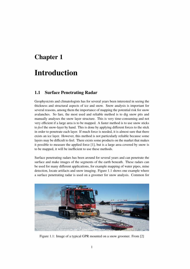
Surface penetrating radars has been around for several years and can penetrate the
surface and make images of the segments of the earth beneath. These radars can
be used for many different applications, for example mapping of water pipes, mine
detection, locate artifacts and snow imaging. Figure 1.1 shows one example where
a surface penetrating radar is used on a groomer for snow analysis. Common for
Figure 1.1: Image of a typical GPR mounted on a snow groomer. From [2]
1

1.1. SURFACE PENETRATING RADAR 2
most of these radar systems, is that they operate in the VHF/UHF band (IEEE
standard 30 MHz-300 MHz/300 MHz-1 GHz [3]). Low frequencies requires large
antenna apertures and for many applications this will be impractical to carry out in
the field.
Lately, a company named Novelda AS has developed a high precision short range
radar (named X2) operating in the C-X band (IEEE standard 4 GHz-12 GHz) [4].
A special version of this radar was created for medical research and is called Ventri-
corder. This model has a lower frequency band which makes it suitable for medical
and snow imaging applications. The Ventricorder operates in the S-C band (IEEE
standard 2 GHz-8 GHz) with a center frequency of 3.9 GHz. The X2 radar can
see through walls with relative high permittivity, which makes it suitable for Snow
Penetrating Radar (SPR) applications [4].
3 CHAPTER 1. INTRODUCTION
1.2 History
Radars has been around for several years, and are often associated with military
usage for airplane and missile detection, or police radar controls. The history of
radar extends all the way back to late 1800 and early 1900, when Heinrich Hertz
(1857 - 1894) first demonstrated reflection of radio waves and Nikola Tesla (1856 -
1943) described a concept for electromagnetic detection and velocity measurements
[5]. The first use of electromagnetic signals for detecting the presence of distant
objects relates back to 1904 and Christian Hülsmeyer (1881-1957). Hülsmeyer
created the first ship collision avoidance system that were able to detect ships up
to a distance of 3 kilometers. This was pioneering work on detection of nearby
ships under foggy weather conditions. However, Hülsmeyers "Telemobiloscope"
was not able to measure distance and target location based on the traditional radar
technology, only the existence of the object [6] [7]. In 1926, Dr. Hülsenbech
introduced the first pulsed radar that were able to determine the structure of buried
features [6] [8]. He discovered that any variations in the dielectrics would reflect
parts of the transmitted signal. In the middle and late 1930s, the United States,
Britain, Germany, France, Russia, Italy and Japan started rapidly the development
of radar systems. In 1936, the US demonstrated the first pulsed radar, and in 1938
they developed the first antiaircraft fire control system, the CCR-268. The same
year, Britain developed their first pulse radar and created the famous Chain Home
surveillance system that was actively used to the end of WW2 [5].
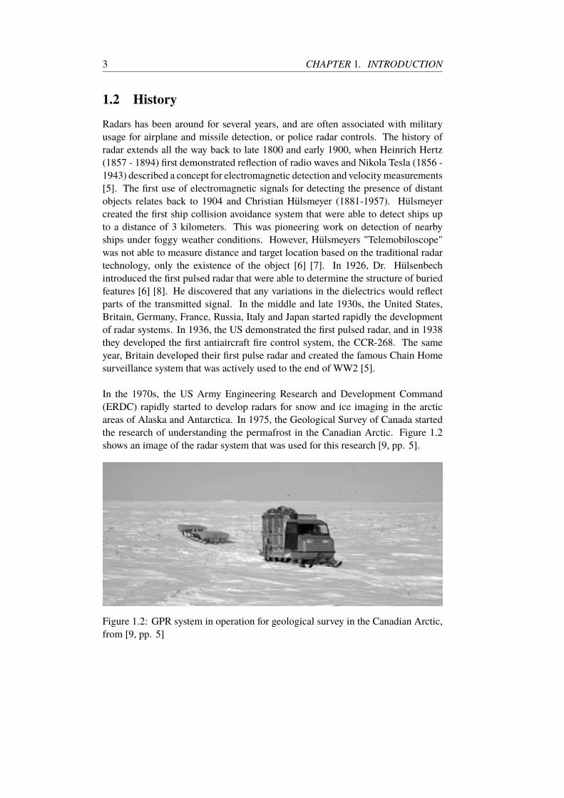
In the 1970s, the US Army Engineering Research and Development Command
(ERDC) rapidly started to develop radars for snow and ice imaging in the arctic
areas of Alaska and Antarctica. In 1975, the Geological Survey of Canada started
the research of understanding the permafrost in the Canadian Arctic. Figure 1.2
shows an image of the radar system that was used for this research [9, pp. 5].
Figure 1.2: GPR system in operation for geological survey in the Canadian Arctic,
from [9, pp. 5]
1.3. MOTIVATION AND GOALS 4
1.3 Motivation and goals
At the University of Oslo there are an on-going transverse collaboration project be-
tween the Department of Geophysics and Department of Informatics called Land-
ATmosphere Interactions in Cold Environments (LATICE). Climate changes im-
pacts the Earth more rapidly, especially in the high latitudes. Therefore, the need of
more highly sophisticated sensors are crucial in order to get a better understanding
of the climate impact of the ice and snow.
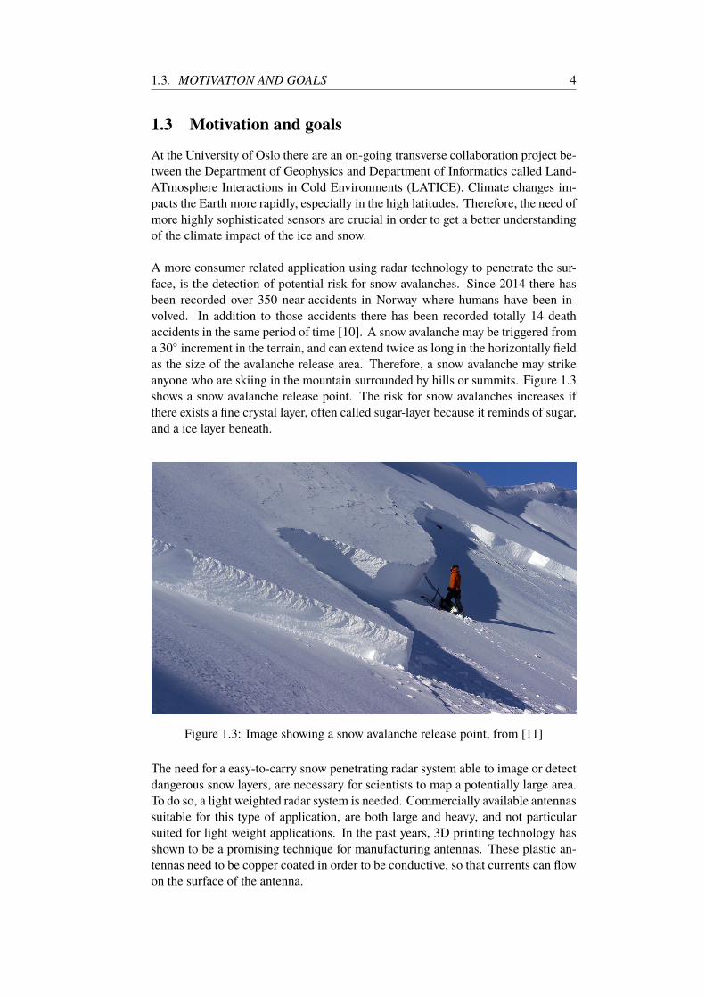
A more consumer related application using radar technology to penetrate the sur-
face, is the detection of potential risk for snow avalanches. Since 2014 there has
been recorded over 350 near-accidents in Norway where humans have been in-
volved. In addition to those accidents there has been recorded totally 14 death
accidents in the same period of time [10]. A snow avalanche may be triggered from
a 30 increment in the terrain, and can extend twice as long in the horizontally field
as the size of the avalanche release area. Therefore, a snow avalanche may strike
anyone who are skiing in the mountain surrounded by hills or summits. Figure 1.3
shows a snow avalanche release point. The risk for snow avalanches increases if
there exists a fine crystal layer, often called sugar-layer because it reminds of sugar,
and a ice layer beneath.
Figure 1.3: Image showing a snow avalanche release point, from [11]
The need for a easy-to-carry snow penetrating radar system able to image or detect
dangerous snow layers, are necessary for scientists to map a potentially large area.
To do so, a light weighted radar system is needed. Commercially available antennas
suitable for this type of application, are both large and heavy, and not particular
suited for light weight applications. In the past years, 3D printing technology has
shown to be a promising technique for manufacturing antennas. These plastic an-
tennas need to be copper coated in order to be conductive, so that currents can flow
on the surface of the antenna.

5 CHAPTER 1. INTRODUCTION
The main goal for this thesis will be to design and develop a light weight 3D printed
antenna, suitable for snow imaging and snow layer detection purposes. This will
require antennas with high gain and large bandwidth in order to get detailed images
of the snow profile.

1.3. MOTIVATION AND GOALS 6
Chapter 2
Background
The purpose of this chapter is to give a brief overview of basic radar concepts with
focus on the dielectric properties, especially for snow. Further, a short introduction
to snow avalanche and snow profiles will be given, followed by a short discussion
of some high gain, ultra-wideband antennas suitable for snow imaging applications.
In the end, parameters for designing a pyramidal horn antenna will be given.
2.1 Fundamentals of RADAR
Radio detection and ranging, or commonly known as RADAR is familiar to most
people. Since the first use of pulsed radars in the early 1900, the development of
many different types of radar systems has rapidly increased. The police traffic radar
is probably common to most people. The principles of radar are much the same as
sound-wave reflection. If one shout in one direction it is often possible to hear the
echo, especially if you are located in the mountains. The radar works in the same
way. An antenna transmit a pulse to a target, either through air or other types of
mediums and the scattered (reflected) signal is received by the same, or a different
antenna depending on the application. Using this concept, radars can be used in a
variety of applications, like imaging, tracking or detection [5, pp. 1-2] [12].
2.1.1 Target detection
In vacuum, electromagnetic waves travels at the speed of light. The total distance
the pulse need to travel for detecting an object, is two times the distance to the
object, or 2R. The traveling time can be found by recording the time between the
transmitted and received pulse. One can therefore express the distance to the object
by the following formula from basic physics [5]
R =c∆t
2(2.1)
where: c = speed of light
∆t = pulse traveling time.
All excising materials have different dielectric properties which will influence the
reflected signal. The dielectric constant is expressed in terms of a real and an
imaginary part. The real part is called the real permittivity which is related to the
7
2.1. FUNDAMENTALS OF RADAR 8
stored energy within the medium. The complex part of the permittivity related
to the dispersion, or losses of energy within the medium. The complex dielectric
constant is given as [13, pp. 37]
ε = ε′ − jε′′ = ε′ − jσ
ωε0
(2.2)
where: ε′ = real part of the permittivity
ε0 = permittivity in vacuum (8.85x10⁻¹²F · m−1)σ = conductivity
ω = frequency.
The velocity of the propagating wave is dependent on the relative permittivity of
the material. Eq. (2.1) assumes that the wave is propagating with a velocity of
speed of light. This is true for vacuum, but for all other materials, this will not be
the case. A more accurate expression for the velocity is expressed as
vr =1
√µε=
1√µ0µrε0εr
(2.3)
where: µ0 = permeability in vacuum (4πx10−7H/m)µr = relative permeability
εr = relative permittivity.
In almost all cases, the relative permeability is equal to one. The expression above
can therefore be simplified to
vr =c
√εr
. (2.4)
Inserting Eq. (2.4) into Eq. (2.1) is necessarily to estimate the distance to the
target. This is especially important for non-air radar applications, like human body
imaging, through wall detection or ground/snow penetrating radar applications
where εr is unequal to one.
2.1.2 Dielectric properties of a material
The dielectric properties of a material describes how the material reacts to
electromagnetic waves. The dielectric constant expressed in Eq. (2.2) consists of
the real permittivity (real part) and a loss factor (imaginary part). The loss tangent
(tanδ) is a ratio between the complex and the real dielectric constant, indicating the
losses in a medium. Mathematically, the loss tangent is expresses as
tanδ =ωε′′ + σ
ωε′. (2.5)
Rewriting Eq. (2.2) by inserting Eq. (2.5), one can express the complex dielectric
constant as
ε = εrε0(1 − jtanδ). (2.6)
For a loss-less materials, the loss factor is equal to zero, which gives a dielectric
constant of [14]
ε = εrε0. (2.7)
9 CHAPTER 2. BACKGROUND
In the real world, such as loss-less materials does not exist. Both the real permittivity
and the loss factor varies depending on the type of material. For SPR applications,
these differences in the dielectric materials is important considerations in order
to determine the different layer structures. This will be discussed more in an
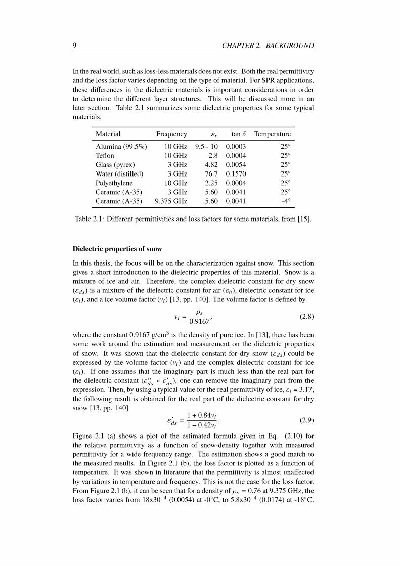
later section. Table 2.1 summarizes some dielectric properties for some typical
materials.
Material Frequency εr tan δ Temperature
Alumina (99.5%) 10 GHz 9.5 - 10 0.0003 25
Teflon 10 GHz 2.8 0.0004 25
Glass (pyrex) 3 GHz 4.82 0.0054 25
Water (distilled) 3 GHz 76.7 0.1570 25
Polyethylene 10 GHz 2.25 0.0004 25
Ceramic (A-35) 3 GHz 5.60 0.0041 25
Ceramic (A-35) 9.375 GHz 5.60 0.0041 -4
Table 2.1: Different permittivities and loss factors for some materials, from [15].
Dielectric properties of snow
In this thesis, the focus will be on the characterization against snow. This section
gives a short introduction to the dielectric properties of this material. Snow is a
mixture of ice and air. Therefore, the complex dielectric constant for dry snow
(εds) is a mixture of the dielectric constant for air (εh), dielectric constant for ice
(εi), and a ice volume factor (vi) [13, pp. 140]. The volume factor is defined by
vi =ρs
0.9167, (2.8)
where the constant 0.9167 g/cm3 is the density of pure ice. In [13], there has been
some work around the estimation and measurement on the dielectric properties
of snow. It was shown that the dielectric constant for dry snow (εds) could be
expressed by the volume factor (vi) and the complex dielectric constant for ice
(εi). If one assumes that the imaginary part is much less than the real part for
the dielectric constant (ε′′ds
« ε′ds
), one can remove the imaginary part from the
expression. Then, by using a typical value for the real permittivity of ice, εi = 3.17,
the following result is obtained for the real part of the dielectric constant for dry
snow [13, pp. 140]
ε′ds =1 + 0.84vi
1 − 0.42vi. (2.9)
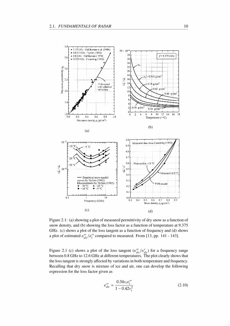
Figure 2.1 (a) shows a plot of the estimated formula given in Eq. (2.10) for
the relative permittivity as a function of snow-density together with measured
permittivity for a wide frequency range. The estimation shows a good match to
the measured results. In Figure 2.1 (b), the loss factor is plotted as a function of
temperature. It was shown in literature that the permittivity is almost unaffected
by variations in temperature and frequency. This is not the case for the loss factor.
From Figure 2.1 (b), it can be seen that for a density of ρs = 0.76 at 9.375 GHz, the
loss factor varies from 18x30−4 (0.0054) at -0C, to 5.8x30−4 (0.0174) at -18C.
2.1. FUNDAMENTALS OF RADAR 10
(a)(b)
(c) (d)
Figure 2.1: (a) showing a plot of measured permittivity of dry snow as a function of
snow density, and (b) showing the loss factor as a function of temperature at 9.375
GHz. (c) shows a plot of the loss tangent as a function of frequency and (d) shows
a plot of estimated ε′′ds/ε′′
icompared to measured. From [13, pp. 141 - 143].
Figure 2.1 (c) shows a plot of the loss tangent (ε′′ds/ε′
ds) for a frequency range
between 0.8 GHz to 12.6 GHz at different temperatures. The plot clearly shows that
the loss tangent is strongly affected by variations in both temperature and frequency.
Recalling that dry snow is mixture of ice and air, one can develop the following
expression for the loss factor given as
ε′′ds =0.34viε
′′i
1 − 0.42v2i
(2.10)
11 CHAPTER 2. BACKGROUND
In Figure 2.1(d), a plot of the loss tangent as a function of snow density is presented
together with measured results at -18 and -0. It can be seen that the estimations
is a good approximation and is close to the measured results.
So far, only dry snow has been discussed. Since wet snow contains of more water,
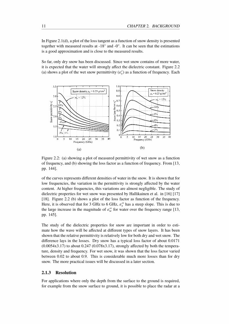
it is expected that the water will strongly affect the dielectric constant. Figure 2.2
(a) shows a plot of the wet snow permittivity (ε′s) as a function of frequency. Each
(a) (b)
Figure 2.2: (a) showing a plot of measured permittivity of wet snow as a function
of frequency, and (b) showing the loss factor as a function of frequency. From [13,
pp. 144].
of the curves represents different densities of water in the snow. It is shown that for
low frequencies, the variation in the permittivity is strongly affected by the water
content. At higher frequencies, this variations are almost negligible. The study of
dielectric properties for wet snow was presented by Hallikainen et al. in [16] [17]
[18]. Figure 2.2 (b) shows a plot of the loss factor as function of the frequency.
Here, it is observed that for 3 GHz to 6 GHz, ε′′s has a steep slope. This is due to
the large increase in the magnitude of ε′′w for water over the frequency range [13,
pp. 145].
The study of the dielectric properties for snow are important in order to esti-
mate how the wave will be affected at different types of snow layers. It has been
shown that the relative permittivity is relatively low for both dry and wet snow. The
difference lays in the losses. Dry snow has a typical loss factor of about 0.0171
(0.0054x3.17) to about 0.247 (0.078x3.17), strongly affected by both the tempera-
ture, density and frequency. For wet snow, it was shown that the loss factor varied
between 0.02 to about 0.9. This is considerable much more losses than for dry
snow. The more practical issues will be discussed in a later section.
2.1.3 Resolution
For applications where only the depth from the surface to the ground is required,
for example from the snow surface to ground, it is possible to place the radar at a
2.1. FUNDAMENTALS OF RADAR 12
specific position and measure the time between the transmitted and received pulse.
However, for most surface penetrating radar applications, it is desirable to see more
information about what is in between the radar and the ground, for example pipe
lines, buried mines, soil layer structure or even snow layer structure, which is the
main focus in this thesis [19]. The radars ability to distinguish between two or
more objects are called resolution. The resolution can be divided into two main
categories; range resolution (downrange) and cross range resolution (often called
azimuth resolution). The range resolution is the ability to detect two or more closely
separated objects in the depth and is directly proportional to the system bandwidth.
The cross range resolution is the ability to detect two or more closely separated
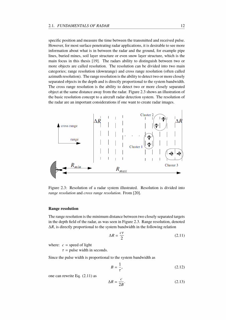
object at the same distance away from the radar. Figure 2.3 shows an illustration of
the basic resolution concept to a aircraft radar detection system. The resolution of
the radar are an important considerations if one want to create radar images.
Figure 2.3: Resolution of a radar system illustrated. Resolution is divided into
range resolution and cross range resolution. From [20].
Range resolution
The range resolution is the minimum distance between two closely separated targets
in the depth field of the radar, as was seen in Figure 2.3. Range resolution, denoted
∆R, is directly proportional to the system bandwidth in the following relation
∆R =cτ
2(2.11)
where: c = speed of light
τ = pulse width in seconds.
Since the pulse width is proportional to the system bandwidth as
B =1
τ, (2.12)
one can rewrite Eq. (2.11) as
∆R =c
2B. (2.13)
13 CHAPTER 2. BACKGROUND
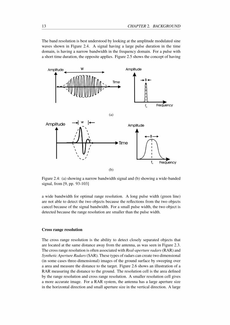
The band resolution is best understood by looking at the amplitude modulated sine
waves shown in Figure 2.4. A signal having a large pulse duration in the time
domain, is having a narrow bandwidth in the frequency domain. For a pulse with
a short time duration, the opposite applies. Figure 2.5 shows the concept of having
(a)
(b)
Figure 2.4: (a) showing a narrow bandwidth signal and (b) showing a wide-banded
signal, from [9, pp. 93-103]
a wide bandwidth for optimal range resolution. A long pulse width (green line)
are not able to detect the two objects because the reflections from the two objects
cancel because of the signal bandwidth. For a small pulse width, the two object is
detected because the range resolution are smaller than the pulse width.
Cross range resolution
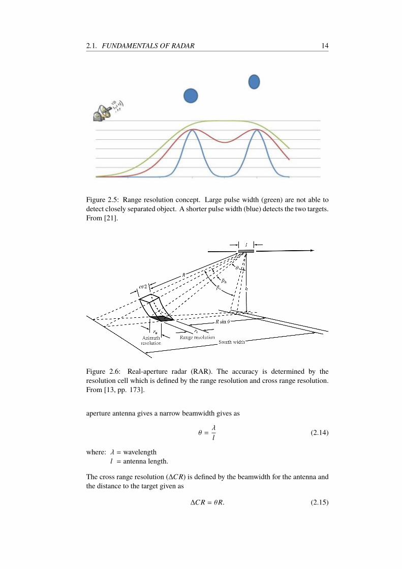
The cross range resolution is the ability to detect closely separated objects that
are located at the same distance away from the antenna, as was seen in Figure 2.3.
The cross range resolution is often associated with Real-aperture radars (RAR) and
Synthetic Aperture Radars (SAR). These types of radars can create two dimensional
(in some cases three-dimensional) images of the ground surface by sweeping over
a area and measure the distance to the target. Figure 2.6 shows an illustration of a
RAR measuring the distance to the ground. The resolution cell is the area defined
by the range resolution and cross range resolution. A smaller resolution cell gives
a more accurate image. For a RAR system, the antenna has a large aperture size
in the horizontal direction and small aperture size in the vertical direction. A large
2.1. FUNDAMENTALS OF RADAR 14
Figure 2.5: Range resolution concept. Large pulse width (green) are not able to
detect closely separated object. A shorter pulse width (blue) detects the two targets.
From [21].
Figure 2.6: Real-aperture radar (RAR). The accuracy is determined by the
resolution cell which is defined by the range resolution and cross range resolution.
From [13, pp. 173].
aperture antenna gives a narrow beamwidth gives as
θ =λ
l(2.14)
where: λ = wavelength
l = antenna length.
The cross range resolution (∆CR) is defined by the beamwidth for the antenna and
the distance to the target given as
∆CR = θR. (2.15)
15 CHAPTER 2. BACKGROUND
Inserting Eq. (2.14) into Eq. (2.15) gives
∆CR =λR
l. (2.16)
The range- and cross range resolution can be used in the radar equation to determine
the total power delivered to the receiving antenna. The total power at a given angle
(θ) is expressed as [13]
〈Prp(θ)〉 =
[
Ptqλ
3G2(θ)cτ2l(4π)3R3sinθ
]
· σ0pq(θ) (2.17)
where: Ptq = power delivered from transmitter
λ = wavelength
G2(θ) = Gain in a direction θ
c = speed of light
τ = pulse width
l = aperture length
R = distance from antenna to target
σ0pq = backscattered cross section per unit area.
2.1.4 Antennas
Antennas are the radar systems “eyes” and “ears’. The Institute of Electrical and
Electronic Engineers (IEEE)’s Standard Definition of Terms for Antennas (IEEE
std. 145-1973) defines an antenna as “a mean for radiating or receiving radio
power”. In practice, the antenna works as a radiating element which acts as a
transducer between an electrical signal in a system and a propagating wave [20].
In many ways, the antenna can be treated as a transmission line between a source
(typically 50Ω) and a load with a given impedance (typically air (377Ω)). The
purpose of the antenna, besides what has been explained, is to focus as much of
the transmitted energy as possible in a decried direction. The field of which the
antenna is able to transmit energy is called the antenna beam. The shape of the
beam is strongly determined by the aperture size. A large antenna aperture results
in a narrow beamwidth. In most radar systems, it is desirable to have a narrow
beamwidth on order to detect closely separated objects [22, pp. 538-539].
A radar antenna is characterized by its gain, radiation pattern, polarization, band-
width and aperture size. In the following sub-sections, each of these terms will be
briefly explained.
Antenna directivity and gain
The directivity of the antenna can be described by the following term [20]
D =maximum radiation intensity
average radiation intensity, (2.18)

2.1. FUNDAMENTALS OF RADAR 16
or expressed by by its solid angles (θ, φ)
D =1
14π
∬
F(θ, φ)dΩ=
4π
ΩA
(2.19)
where: ΩA = beam solid angle.
However, a more approximate expression for the directivity can be made by
assuming that the antenna has one narrow major lobe and very negligible minor
lobes. Eq. (2.19) can thereby be written as
D =4π
Θ1rΘ2r
(2.20)
where: Θ1r = half-power beamwidth in one plane (rad)
Θ2r = half-power beamwidth in a plane at a right angle to the other (rad).
The gain describes how much of the radiated signal that is concentrated in a given
direction. The gain for an antenna is directly related to the directivity. In fact of
one neglects the antenna losses, the gain is equal to the directivity. Therefore, the
gain can be expressed as a function of the directivity times a efficiency constant, or
[23, pp. 19-25]
G = De0 (2.21)
where: D = directivity
e0 = efficiency.
Radiation pattern
The radiation pattern gives a graphical representation of the antenna radiation
properties. This can be represented in several ways; field patter (linear scale),
power pattern in linear scale and power pattern in decibel scale. The most common
is to define the pattern in order of power in dB. The angle of the beam (beamwidth)
is defined by its half-power beam width (HPBW), which is defined by the -3 dB
point from the maximum directivity [23, pp. 3-5].
Polarization
The polarization of the antenna defined as the “property of an electromagnetic wave
describing the time-varying direction and relative magnitude of the electric-field
vector; specifically, the figure traced as a function of time by the extremity of the
vector at a fixed location in space, and the sense in which it is traced, as observed
along the direction of propagation” [23, pp. 27]. The polarization can be either
linear, circular or elliptical. In this thesis, only linear polarized antennas will be
discussed.

17 CHAPTER 2. BACKGROUND
Bandwidth
The bandwidth of an antenna does not have a common definition applying for all
types of antennas. For example, for a wideband antenna the bandwidth is defined
for its upper and lower frequency in the acceptable value of either input impedance,
pattern, beamwidth, polarization, side lobe level, gain, beam direction or, radiation
efficiency. For a narrow band antenna the bandwidth is defines as a percentage of
the upper and lower frequency difference over the center frequency [23, pp. 26].
In this thesis, the bandwidth will be defined by the upper and lower frequency at
which point the reflected signal is 10 %, or -10 dB of the transmitted signal.
Effective aperture
For an effective antenna the gain is approximately equal to the beam pattern. The
efficiency of the aperture is given by the following expression
Ae =P
W(2.22)
where: P = Power delivered to the antenna
W =Wave power density
The effective aperture is defined as; “The effective aperture is the area Ae such that,
if all the power incident on the area was collected and delivered to the load with
no loss, it would account for all the observed power outputs of the actual antenna”
[5, pp.11 - 12]. Knowing the effective aperture, one can express the directivity of
a antenna as
D =4π
λ2Ae (2.23)
where: λ = wavelength
2.2. USING RADAR FOR SNOW IMAGING 18
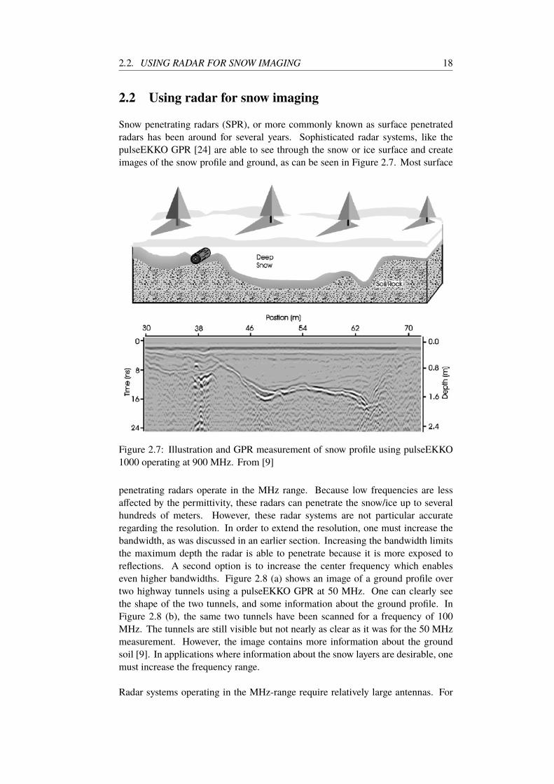
2.2 Using radar for snow imaging
Snow penetrating radars (SPR), or more commonly known as surface penetrated
radars has been around for several years. Sophisticated radar systems, like the
pulseEKKO GPR [24] are able to see through the snow or ice surface and create
images of the snow profile and ground, as can be seen in Figure 2.7. Most surface
Figure 2.7: Illustration and GPR measurement of snow profile using pulseEKKO
1000 operating at 900 MHz. From [9]
penetrating radars operate in the MHz range. Because low frequencies are less
affected by the permittivity, these radars can penetrate the snow/ice up to several
hundreds of meters. However, these radar systems are not particular accurate
regarding the resolution. In order to extend the resolution, one must increase the
bandwidth, as was discussed in an earlier section. Increasing the bandwidth limits
the maximum depth the radar is able to penetrate because it is more exposed to
reflections. A second option is to increase the center frequency which enables
even higher bandwidths. Figure 2.8 (a) shows an image of a ground profile over
two highway tunnels using a pulseEKKO GPR at 50 MHz. One can clearly see
the shape of the two tunnels, and some information about the ground profile. In
Figure 2.8 (b), the same two tunnels have been scanned for a frequency of 100
MHz. The tunnels are still visible but not nearly as clear as it was for the 50 MHz
measurement. However, the image contains more information about the ground
soil [9]. In applications where information about the snow layers are desirable, one
must increase the frequency range.
Radar systems operating in the MHz-range require relatively large antennas. For

19 CHAPTER 2. BACKGROUND
(a)
(b)
Figure 2.8: (a) showing an image scan using pulseEKKO at 50 MHz, and (b) is
showing a scan from the same radar at 100 Mhz. From [9]
remote Geo-Sensing applications, it is desirable to have a radar system that is easy
to carry out in the field. Also, for detection of possible risk of snow avalanche
the need for long depth measurements are not particularly interesting. Instead,
more information about the snow profile is the main goal. In fact, increasing the
frequency and hence the bandwidth is crucial for detecting different layers in the
snow. This will be discussed in the next section.
2.2.1 Snow avalanches
The risk of potential snow avalanche exists in all areas where the mountain or hill
has a 30 slope or more. The avalanche area is often divided into two main zones;
starting zone and deposition zone. The staring zone is the area where the potential
risk of an avalanche can occur. The deposition zone is the area where the avalanche
may strike and can be two times as long as the starting zone [25].
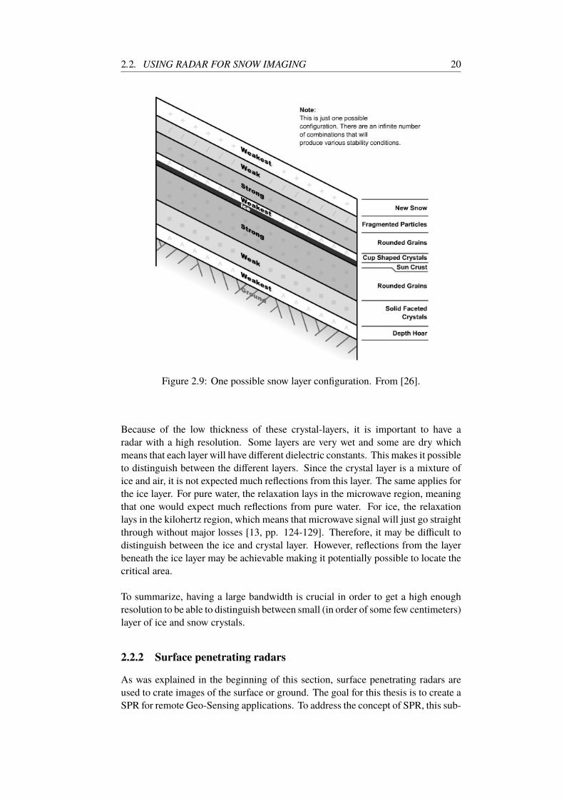
Over time, temperature and wind will change the snow characteristic and cre-
ate different layers in the snow pack. Figure 2.9 shows a typical snow pack with
different layers. In the middle of the figure, it is shown two layers indicated Weakest
and Ice. These two layers are the main reason for an avalanche to happen. The
weakest layer can be as thin as one centimeter and up to some few centimeters thick
and consists of snow crystals formed during cold and windy conditions. The crys-
tals looks like sugar, and is therefore often called sugar-layer. If a crystal-layer lays
on top of a ice layer as seen in the figure, the hole snow pack above the crystal-layer
will eventually start to glide if the slope is steep, or if it gets triggered by a skier or
by weather conditions.
2.2. USING RADAR FOR SNOW IMAGING 20
Figure 2.9: One possible snow layer configuration. From [26].
Because of the low thickness of these crystal-layers, it is important to have a
radar with a high resolution. Some layers are very wet and some are dry which
means that each layer will have different dielectric constants. This makes it possible
to distinguish between the different layers. Since the crystal layer is a mixture of
ice and air, it is not expected much reflections from this layer. The same applies for
the ice layer. For pure water, the relaxation lays in the microwave region, meaning
that one would expect much reflections from pure water. For ice, the relaxation
lays in the kilohertz region, which means that microwave signal will just go straight
through without major losses [13, pp. 124-129]. Therefore, it may be difficult to
distinguish between the ice and crystal layer. However, reflections from the layer
beneath the ice layer may be achievable making it potentially possible to locate the
critical area.
To summarize, having a large bandwidth is crucial in order to get a high enough
resolution to be able to distinguish between small (in order of some few centimeters)
layer of ice and snow crystals.
2.2.2 Surface penetrating radars
As was explained in the beginning of this section, surface penetrating radars are
used to crate images of the surface or ground. The goal for this thesis is to create a
SPR for remote Geo-Sensing applications. To address the concept of SPR, this sub-
21 CHAPTER 2. BACKGROUND
sections starts by explaining the basic concept of GPRs as these two applications
uses the same type of technology.
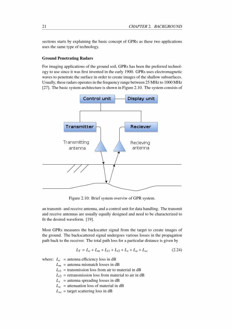
Ground Penetrating Radars
For imaging applications of the ground soil, GPRs has been the preferred technol-
ogy to use since it was first invented in the early 1900. GPRs uses electromagnetic
waves to penetrate the surface in order to create images of the shallow subsurfaces.
Usually, these radars operates in the frequency range between 25 MHz to 1000 MHz
[27]. The basic system architecture is shown in Figure 2.10. The system consists of
Figure 2.10: Brief system overviw of GPR system.
an transmit- and receive antenna, and a control unit for data handling. The transmit
and receive antennas are usually equally designed and need to be characterized to
fit the desired waveform. [19].
Most GPRs measures the backscatter signal from the target to create images of
the ground. The backscattered signal undergoes various losses in the propagation
path back to the receiver. The total path loss for a particular distance is given by
LT = Le + Lm + Lt1 + Lt2 + Ls + La + Lsc (2.24)
where: Le = antenna efficiency loss in dB
Lm = antenna mismatch losses in dB
Lt1 = transmission loss from air to material in dB
Lt2 = retransmission loss from material to air in dB
Ls = antenna spreading losses in dB
La = attenuation loss of material in dB
Lsc = target scattering loss in dB
2.2. USING RADAR FOR SNOW IMAGING 22
To get a accurate prediction of the losses, this calculation has to be performed for
the frequencies of interest. Equations for calculating the different losses can be
found in the literature [19].
Depth measurement using GPR
The dielectric properties of the medium is often unknown. Therefore, for a practical
measurement, the velocity has to be estimated by means of multiple measurements.
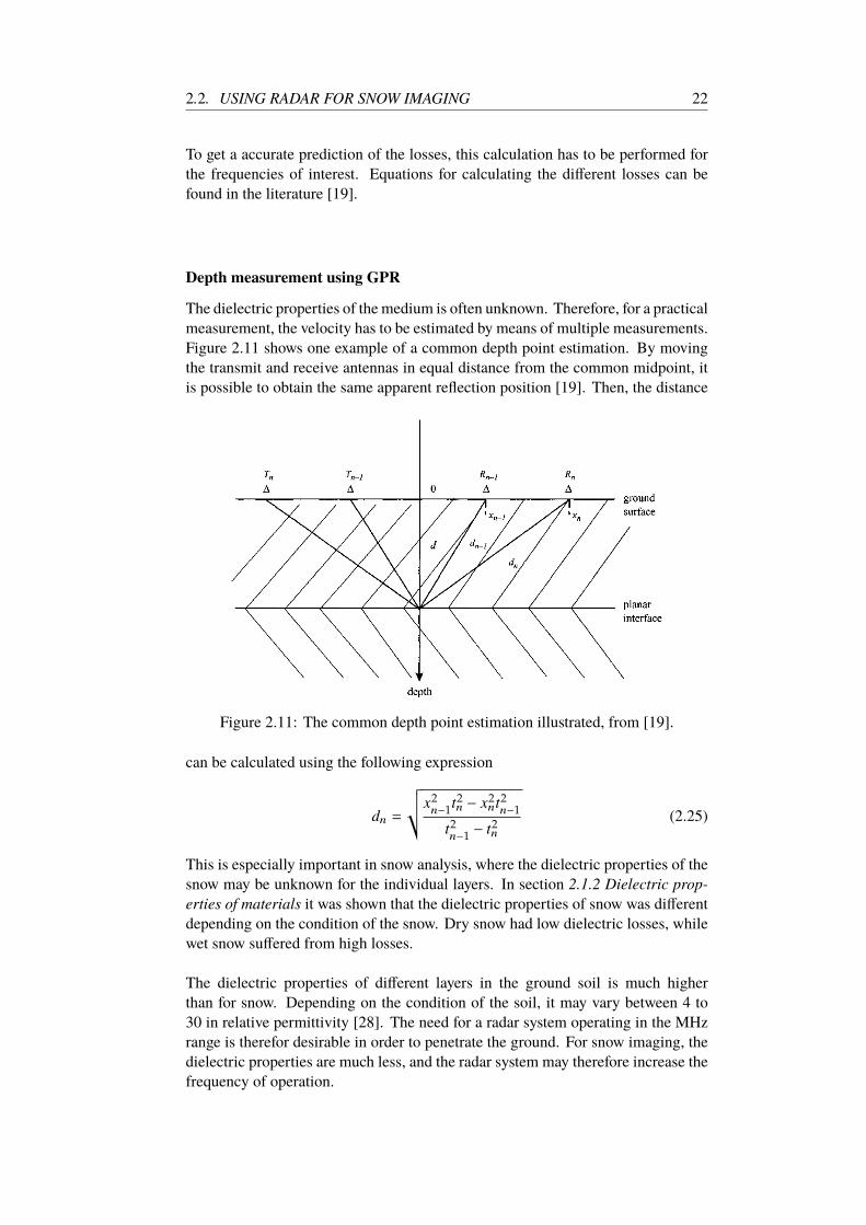
Figure 2.11 shows one example of a common depth point estimation. By moving
the transmit and receive antennas in equal distance from the common midpoint, it
is possible to obtain the same apparent reflection position [19]. Then, the distance
Figure 2.11: The common depth point estimation illustrated, from [19].
can be calculated using the following expression
dn =
√
√
x2n−1
t2n − x2
nt2n−1
t2n−1
− t2n
(2.25)
This is especially important in snow analysis, where the dielectric properties of the
snow may be unknown for the individual layers. In section 2.1.2 Dielectric prop-
erties of materials it was shown that the dielectric properties of snow was different
depending on the condition of the snow. Dry snow had low dielectric losses, while
wet snow suffered from high losses.
The dielectric properties of different layers in the ground soil is much higher
than for snow. Depending on the condition of the soil, it may vary between 4 to
30 in relative permittivity [28]. The need for a radar system operating in the MHz
range is therefor desirable in order to penetrate the ground. For snow imaging, the
dielectric properties are much less, and the radar system may therefore increase the
frequency of operation.
23 CHAPTER 2. BACKGROUND
Snow penetrating radars
SPRs works much in the same way as a GPR. The difference lays in the potential us-
age of the frequency of operation, as was discussed above. Imaging and measuring
depth of glaciers was one of the first applications where SPRs were used. Since the
ice almost has a constant permittivity as a function of temperature (approximately
3.2), it is easy for the electromagnetic waves to penetrate the glacier [29]. Most of
the work related to snow and ice is related to glaciers and not so much regarding
snow profile imaging with respect to snow avalanches.
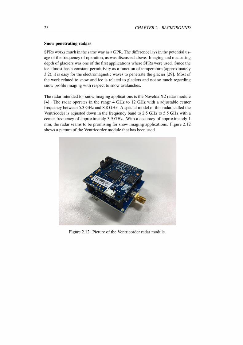
The radar intended for snow imaging applications is the Novelda X2 radar module
[4]. The radar operates in the range 4 GHz to 12 GHz with a adjustable center
frequency between 5.3 GHz and 8.8 GHz. A special model of this radar, called the
Ventricoder is adjusted down in the frequency band to 2.5 GHz to 5.5 GHz with a
center frequency of approximately 3.9 GHz. With a accuracy of approximately 1
mm, the radar seams to be promising for snow imaging applications. Figure 2.12
shows a picture of the Ventricorder module that has been used.
Figure 2.12: Picture of the Ventricorder radar module.
2.3. DIRECTIONAL UWB ANTENNAS FOR SNOW IMAGING 24
2.3 Directional UWB Antennas for snow imaging
As has been discussed in the previous sections, it is desirable to have a large signal
bandwidth in order to get a good resolution for the SPR image. To accomplish this,
the transmit and receive antennas needs to have sufficient bandwidth to meet this
requirement. An antenna having a narrow bandwidth will result in oscillations and
stretching of the propagating signal.
In addition to an antenna having a large bandwidth, it is important to have a
large gain and narrow beamwidth. For snow imaging applications, this is essential
for getting reliable measurements. As the signal is propagating down into the snow,
the receive antenna will pick up reflections from each snow-layer. If the antenna
has a wide beamwidth, the receive antenna will pick up multiple reflections from
multiple layers at the same time. It will therefore be difficult to distinguish between
the different layers. Having a narrow beamwidth (ideally as the beam of a laser),
the receive antenna will see reflections from the different layers at different times.
This makes it easier to distinguish between the different layers.
For remote Geo-Sensing applications like SAR or RAR imaging, it is essential
to have a radar system that is mobile and easy to carry out in the field. A large radar
system would be impractical for many applications, especially avalanche detection
where measuring the mountain side with slopes steeper than 30 is the critical part.
Weight and size is two important considerations that needs to be evaluated along
with the gain and bandwidth requirements.
During the past years, 3D printed antennas has shown to be a promising tech-
nology regarding light weighted antennas [30] [31]. These antennas are printed
in low cost plastic (PLA) and coated with copper spray, or electroplated to make
the surface conductive. In this section, a selection of different high gain, ultra-
wideband (UWB) antennas will be shown, in addition to a discussion of the weight
and size with respect to the intended application.
2.3.1 Reflector antennas
Reflector antennas was first introduced by Heinrich Hertz (1857 - 1894) in 1887.
The reflector antenna, or parabolic antennas are known to most people and are
often used for television signals, wireless LAN, satellite communication and as
radar antennas. These antennas are popular for end to end applications where high
gain is desired [32]. Reflector antennas are categorized into the main classes; planar
reflectors, corner reflectors and parabolic cylinder reflectors are some of them. In
this section, only the parabolic reflector will be examined because of its high gain
and relatively large bandwidth [33].
Parabolic reflector antenna
Parabolic reflector antennas can be designed for very high gain (in the order 30
dBi). The focal length of a reflector antenna determines the dimensions. If the
vertex lies at the origin and the parabola is oriented towards the positive y-axis with
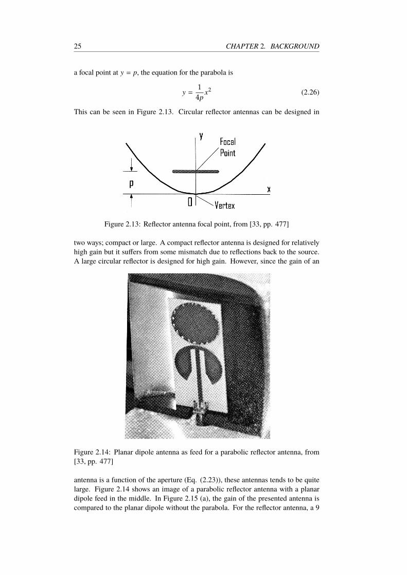
25 CHAPTER 2. BACKGROUND
a focal point at y = p, the equation for the parabola is
y =1
4px2 (2.26)
This can be seen in Figure 2.13. Circular reflector antennas can be designed in
Figure 2.13: Reflector antenna focal point, from [33, pp. 477]
two ways; compact or large. A compact reflector antenna is designed for relatively
high gain but it suffers from some mismatch due to reflections back to the source.
A large circular reflector is designed for high gain. However, since the gain of an
Figure 2.14: Planar dipole antenna as feed for a parabolic reflector antenna, from
[33, pp. 477]
antenna is a function of the aperture (Eq. (2.23)), these antennas tends to be quite
large. Figure 2.14 shows an image of a parabolic reflector antenna with a planar
dipole feed in the middle. In Figure 2.15 (a), the gain of the presented antenna is
compared to the planar dipole without the parabola. For the reflector antenna, a 9
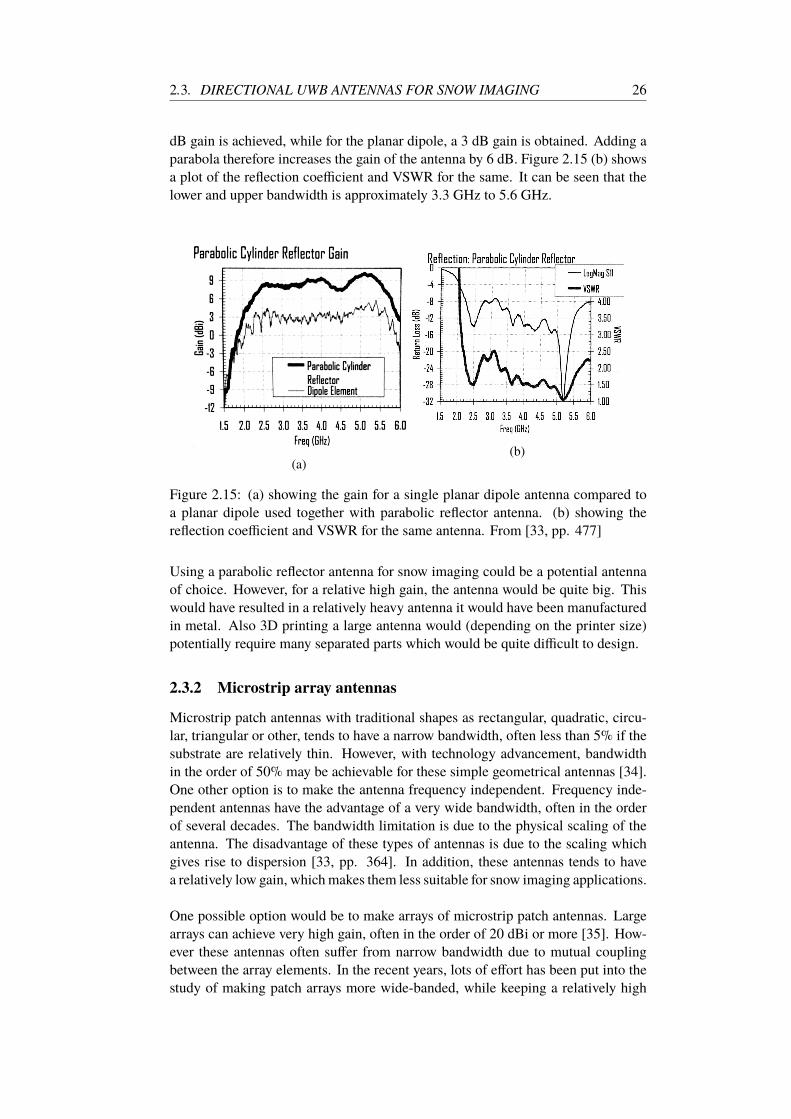
2.3. DIRECTIONAL UWB ANTENNAS FOR SNOW IMAGING 26
dB gain is achieved, while for the planar dipole, a 3 dB gain is obtained. Adding a
parabola therefore increases the gain of the antenna by 6 dB. Figure 2.15 (b) shows
a plot of the reflection coefficient and VSWR for the same. It can be seen that the
lower and upper bandwidth is approximately 3.3 GHz to 5.6 GHz.
(a)(b)
Figure 2.15: (a) showing the gain for a single planar dipole antenna compared to
a planar dipole used together with parabolic reflector antenna. (b) showing the
reflection coefficient and VSWR for the same antenna. From [33, pp. 477]
Using a parabolic reflector antenna for snow imaging could be a potential antenna
of choice. However, for a relative high gain, the antenna would be quite big. This
would have resulted in a relatively heavy antenna it would have been manufactured
in metal. Also 3D printing a large antenna would (depending on the printer size)
potentially require many separated parts which would be quite difficult to design.
2.3.2 Microstrip array antennas
Microstrip patch antennas with traditional shapes as rectangular, quadratic, circu-
lar, triangular or other, tends to have a narrow bandwidth, often less than 5% if the
substrate are relatively thin. However, with technology advancement, bandwidth
in the order of 50% may be achievable for these simple geometrical antennas [34].
One other option is to make the antenna frequency independent. Frequency inde-
pendent antennas have the advantage of a very wide bandwidth, often in the order
of several decades. The bandwidth limitation is due to the physical scaling of the
antenna. The disadvantage of these types of antennas is due to the scaling which
gives rise to dispersion [33, pp. 364]. In addition, these antennas tends to have
a relatively low gain, which makes them less suitable for snow imaging applications.
One possible option would be to make arrays of microstrip patch antennas. Large
arrays can achieve very high gain, often in the order of 20 dBi or more [35]. How-
ever these antennas often suffer from narrow bandwidth due to mutual coupling
between the array elements. In the recent years, lots of effort has been put into the
study of making patch arrays more wide-banded, while keeping a relatively high

27 CHAPTER 2. BACKGROUND
gain. It was observed that if a bandwidth of 10:1 was to be achieved, the maximum
area of the unit cell has to be no longer than 0.05 times the wavelength at the lowest
frequency. If the radiating elements exceeded 0.5 wavelength, grating lobes and
surface waves starts to appear in the frequency band. One type of patch antenna
that offer high gain and wide bandwidth is the current sheet array, which will be
discussed in the next sub-section [36].
Current sheet antenna array
In 1999, Harris Corporation together with Dr. Ben Munk developed the first current
sheet antenna array (CSA) based on a requirement of a 9:1 bandwidth antenna array
targeted for 2 - 18 GHz operation. Harris and Muck discovered that a closely spaced
overlapping dipole array exhibits a wide bandwidth when employed as an frequency
selective surface (FSS) antenna. Due to the overlap capacitance between the ele-
ments, an array of dipoles with a small elements spacing above the ground plane
could achieve a relatively high bandwidth. In order to extend this theory to obtain
a even wider bandwidth, Harris and Munk discovered that by adding a dielectric
layer on top of the dipole arrays, one would obtain an even wider bandwidth. The
results showed that for a VSWR of 2:1, a bandwidth of 7:1 was obtained [36].
Figure 2.16 (a) shows an image of a CSA patented by Munk and Harris [37].
The image shows an early stage of the CSA with a 12-in x 18-in array. The in-
terdigital capacitors shown in Figure 2.16 (b) ensures capacitive coupling between
the elements [37]. In a later development, a 22-in x 22-in dual-polarized array was
(a)
(b)
Figure 2.16: (a) showing the antenna array for a current sheet array (CSA), and (b)
showing the interdigital capacitors. From [37]
created to meet the original requirement for a bandwidth between 2 to 18 GHz.
2.3. DIRECTIONAL UWB ANTENNAS FOR SNOW IMAGING 28
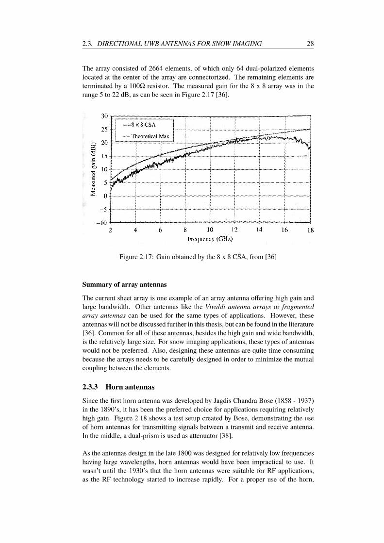
The array consisted of 2664 elements, of which only 64 dual-polarized elements
located at the center of the array are connectorized. The remaining elements are
terminated by a 100Ω resistor. The measured gain for the 8 x 8 array was in the
range 5 to 22 dB, as can be seen in Figure 2.17 [36].
Figure 2.17: Gain obtained by the 8 x 8 CSA, from [36]
Summary of array antennas
The current sheet array is one example of an array antenna offering high gain and
large bandwidth. Other antennas like the Vivaldi antenna arrays or fragmented
array antennas can be used for the same types of applications. However, these
antennas will not be discussed further in this thesis, but can be found in the literature
[36]. Common for all of these antennas, besides the high gain and wide bandwidth,
is the relatively large size. For snow imaging applications, these types of antennas
would not be preferred. Also, designing these antennas are quite time consuming
because the arrays needs to be carefully designed in order to minimize the mutual
coupling between the elements.
2.3.3 Horn antennas
Since the first horn antenna was developed by Jagdis Chandra Bose (1858 - 1937)
in the 1890’s, it has been the preferred choice for applications requiring relatively
high gain. Figure 2.18 shows a test setup created by Bose, demonstrating the use
of horn antennas for transmitting signals between a transmit and receive antenna.
In the middle, a dual-prism is used as attenuator [38].
As the antennas design in the late 1800 was designed for relatively low frequencies
having large wavelengths, horn antennas would have been impractical to use. It
wasn’t until the 1930’s that the horn antennas were suitable for RF applications,
as the RF technology started to increase rapidly. For a proper use of the horn,

29 CHAPTER 2. BACKGROUND
Figure 2.18: The figure is showing a test setup using one of the first invented horn
antennas created by J. C. Bose in the 1890’s. The transmit antenna can be seen to
the left, while the receive antenna is to the right. From [38].
the length of the antenna is almost a wavelength long, resulting in large apertures
which leads to directional antennas with relatively high gains. Lots of research has
been developed for these types of antennas. In 1937, Wilmer L. Barrow (1903 -
1973) and Len Jen Chu (1913 -1973) described the physics of the horn antenna,
and Schelkunoff and Friis has developed excellent equations for horn design calcu-
lations [33] [39].
The horn antenna acts as a flared or tapered transmission line designed to transmit
and receive electromagnetic waves. Besides of having a relatively high gain, these
antennas tend to have a narrow bandwidth. In order to increase the bandwidth,
one can add a tapered ridged waveguide which lowers the cut-off frequency of the
dominant mode, and increase the cut-off frequency for the next dominant mode
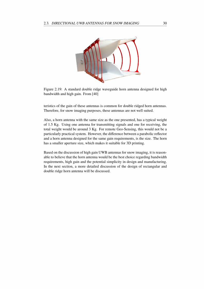
[33]. A good selection of these types of horn antennas exists on the market. Figure
2.19 shows a typical double ridged waveguide horn antenna. The aperture size
is 15.9 cm x 24.2 cm and the length is 27.9 cm. The antenna is designed for a
bandwidth between 750 MHz and 18 GHz. At 750 MHz the gain is about 2.6 dBi,
but at 1 GHz it reaches approximately 7 dBi. Between 3 GHz and up to 8 GHz,
the antenna has a almost linear gain between 10 dBi and 12 dBi. The antenna is
matched with an maximum VSWR of 5:1, but typically in the range 2:1 above 800
MHz [40]. Typical half-power beamwidth (HPBW) are 30-40 in the H-plane, and
45 in the E-plane [33].
For snow imaging purposes, it is desirable to have a almost linear gain over the
entire frequency band. It was shown in Figure 2.15 (a) for the parabolic reflector
that the gain was close to flat over a band between 2.5 GHz to 5.5 GHz. This is
not the case for the double ridge waveguide horn that was described. This charac-
2.3. DIRECTIONAL UWB ANTENNAS FOR SNOW IMAGING 30
Figure 2.19: A standard double ridge waveguide horn antenna designed for high
bandwidth and high gain. From [40]
teristics of the gain of these antennas is common for double ridged horn antennas.
Therefore, for snow imaging purposes, these antennas are not well suited.
Also, a horn antenna with the same size as the one presented, has a typical weight
of 1.5 Kg. Using one antenna for transmitting signals and one for receiving, the
total weight would be around 3 Kg. For remote Geo-Sensing, this would not be a
particularly practical system. However, the difference between a parabolic reflector
and a horn antenna designed for the same gain requirements, is the size. The horn
has a smaller aperture size, which makes it suitable for 3D printing.
Based on the discussion of high gain UWB antennas for snow imaging, it is reason-
able to believe that the horn antenna would be the best choice regarding bandwidth
requirements, high gain and the potential simplicity in design and manufacturing.
In the next section, a more detailed discussion of the design of rectangular and
double ridge horn antenna will be discussed.
31 CHAPTER 2. BACKGROUND
2.4 Horn antenna parameters
A quick history and a example of the performance of the horn antenna was given
in the previous section. The purpose of this section is to give the reader a detailed
discussion of the design procedures and parameters obtained to create a rectangular
horn antenna. A traditional rectangular horn antenna is divided intro three main
parts; feed, waveguide and horn aperture. Each of these parts will be discussed in
this section stating with the waveguide. Then the feeding technique of rectangular
waveguides will be discussed, followed by the design parameters for a rectangular
horn antenna.
2.4.1 Waveguide design parameters
A waveguide is an transmission medium for effectively transmitting electromagnetic
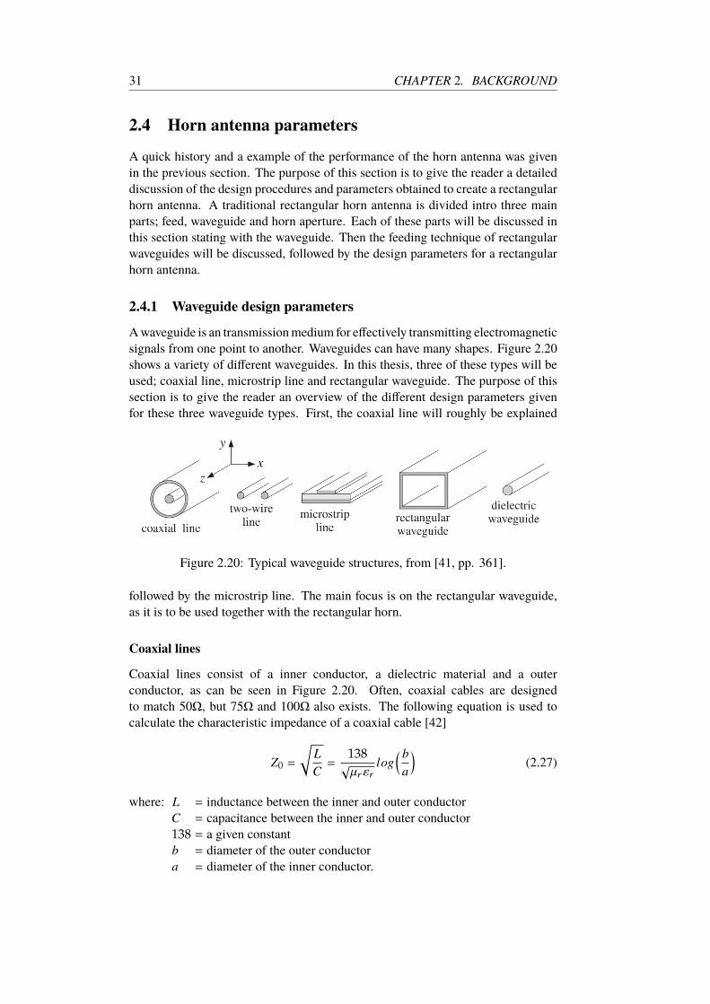
signals from one point to another. Waveguides can have many shapes. Figure 2.20
shows a variety of different waveguides. In this thesis, three of these types will be
used; coaxial line, microstrip line and rectangular waveguide. The purpose of this
section is to give the reader an overview of the different design parameters given
for these three waveguide types. First, the coaxial line will roughly be explained
Figure 2.20: Typical waveguide structures, from [41, pp. 361].
followed by the microstrip line. The main focus is on the rectangular waveguide,
as it is to be used together with the rectangular horn.
Coaxial lines
Coaxial lines consist of a inner conductor, a dielectric material and a outer
conductor, as can be seen in Figure 2.20. Often, coaxial cables are designed
to match 50Ω, but 75Ω and 100Ω also exists. The following equation is used to
calculate the characteristic impedance of a coaxial cable [42]
Z0 =
√
L
C=
138√µrεr
log( b
a
)
(2.27)
where: L = inductance between the inner and outer conductor
C = capacitance between the inner and outer conductor
138 = a given constant
b = diameter of the outer conductor
a = diameter of the inner conductor.
2.4. HORN ANTENNA PARAMETERS 32
Microstrip lines
A PCB transmission line can have many shapes and forms. In this thesis, only
equations for the microstrip transmission line will be given. Other types can be
found in literature [33, pp. 140]. The microstrip line is a single strip-line on one
side of a PCB with a ground plane on the other side, separated by a dielectric.
The equations for the characteristic impedance is a function of the height of the
substrate, width of the trace and the dielectric constant for the substrate, given as
Z0 =120π
√εe f f ·
[
WH+ 1.393 + 2
3ln
(
WH+ 1.444
)] (2.28)
where: εe f f = effective dielectric constant
W = width of the strip line
H = height of the substrate
the effective dielectric constant is given by
εe f f =εr + 1
2+
εr − 1
2
(
1 + 12
(
H
W
)]−1/2
(2.29)
where: εr = relative dielectric constant
Rectangular waveguides
Designing a rectangular waveguide is mainly based on the requirements for the
center- and cutoff frequency for the system. The general equation for the cut-off
frequency are given as
fc =1
2√εµ
√
(m
a
)2
+
(n
b
)2
, (2.30)
where: ε = dielectric constant
µ = permeability constant
a = width of the waveguide
b = height of the waveguide
m, n = integers defining number of half-wavelengths that will fit in a and b
dimensions, respectively.
The integers m, and n is determined by the selection of the propagation mode.
Rectangular waveguides support different propagation modes. These are called the
transverse electric mode and transverse magnetic mode, denoted TEmn and T Mmn.
The index m indicates the number of half-wavelength variations in the width of the
waveguide (a), and the index n is the number of half-wavelength variations in the
height (b). Figure 2.21 (a) shows an image of one single mode propagating in the
rectangular waveguide. For this mode, the electric (green) and magnetic (blue) field
are perpendicular to each other. Figure 2.21 (b) shows two propagating modes. In

33 CHAPTER 2. BACKGROUND
(a) (b)
Figure 2.21: (a) showing one single propagating mode, and (b) showing two
propagating modes. From [43]
this thesis, only modes propagating in the TE10 mode is considered. Therefore, Eq.
(2.30) can be expressed as
fc =1
2a√εµ
. (2.31)
The most common way to express the cut-off wavelength for a waveguide is by the
following expression
λc =2
√
(
ma
)2+
(
nb
)2. (2.32)
Of course, this is just another way to express the relation
λc =c
fc(2.33)
Inside the waveguide there is something called the guided-wavelength. The guided
wavelength is the distance between two equal phases along the waveguide section,
and is expresses by the cut-off frequency and the center frequency in the following
relation.
λg =λ0
√
1 −( fcf
)2, (2.34)
where: λg = wavelength in waveguide
λ0 = wavelength in free space
fc = waveguide cut-off frequency
f = operating frequency.
Using all of this equations, one can calculate the dimensions for the waveguide
based on the cut-off frequency and the center frequency.
2.4. HORN ANTENNA PARAMETERS 34
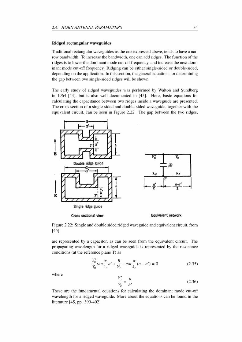
Ridged rectangular waveguides
Traditional rectangular waveguides as the one expressed above, tends to have a nar-
row bandwidth. To increase the bandwidth, one can add ridges. The function of the
ridges is to lower the dominant mode cut-off frequency, and increase the next dom-
inant mode cut-off frequency. Ridging can be either single-sided or double-sided,
depending on the application. In this section, the general equations for determining
the gap between two single-sided ridges will be shown.
The early study of ridged waveguides was performed by Walton and Sundberg
in 1964 [44], but is also well documented in [45]. Here, basic equations for
calculating the capacitance between two ridges inside a waveguide are presented.
The cross section of a single-sided and double-sided waveguide, together with the
equivalent circuit, can be seen in Figure 2.22. The gap between the two ridges,
Figure 2.22: Single and double sided ridged waveguide and equivalent circuit, from
[45].
are represented by a capacitor, as can be seen from the equivalent circuit. The
propagating wavelength for a ridged waveguide is represented by the resonance
conditions (at the reference plane T) as
Y ′0
Y0
tanπ
λca′+
B
Y0
− cotπ
λc(a − a′) = 0 (2.35)
whereY ′
0
Y0
=
b
b′(2.36)
These are the fundamental equations for calculating the dominant mode cut-off
wavelength for a ridged waveguide. More about the equations can be found in the
literature [45, pp. 399-402]

35 CHAPTER 2. BACKGROUND
2.4.2 Feeding techniques for rectangular waveguides
Feeding a rectangular waveguide is traditionally done by probing a coaxial stub a
quarter of a wavelength down into the waveguide. More on this technique and other
is explained in a later chapter.
2.4.3 Horn design parameters
As has been discussed, horn antennas can be designed for a large gain, often
more than 12 dBi. Figure 2.23 shows the typical design parameters for a standard
rectangular horn antenna. The equations for calculating the dimensions of the horn
Figure 2.23: Typical horn shape. (a) showing a 3D model of the horn shape, (b)
shows a cross section of the side and (c) shows the cross section from the top. from
[46, pp. 101].
is based on the desired gain and the size of the waveguide. The following equations
2.4. HORN ANTENNA PARAMETERS 36
is given as [46, pp. 118-119]
Gl = 10GdBi/10 (2.37)
A = 0.096aG0.232l + 0.42λG0.503
l − 0.193b (2.38)
RH = A
√
√
√
1
A+
(
A
3λ
)2
(2.39)
LH = (A− a)
√
√
√(
RH
A
)2
− 1
4(2.40)
DH =
√
√
√
R2H−
(
A
2
)2
(2.41)
B =1
2
[
b+√
b2+ 8LHλ
]
(2.42)
RE =B
2
√
√
√
1 +
(
B
λ
)2
(2.43)
LE = (B − b)
√
√
√(
RB
B
)2
− 1
4(2.44)
DE =
√
√
√
R2E−
(
B
2
)2
. (2.45)
2.4.4 Summary of horn antenna parameters
This section gives a brief overview over the basic design parameters for designing a
rectangular horn antenna and a ridged waveguide. Designing a rectangular horn is
quite straight forward if the center frequency, cut-off frequency and gain is known.
Designing a ridged waveguide is more challenging if the design equations are to
be used. For this particular design, a more methodical design approach would
probably more preferred for time saving.
37 CHAPTER 2. BACKGROUND
2.5 System overview
The main goal in this thesis is to create an ultra-wideband (UWB) 3D printed
antenna suitable for snow imaging purposes. Such a system requires specific
specifications for the bandwidth considering resolution and the performance of the
Novelda radar module. In addition, high gain over the entire bandwidth is desirable
so that the antenna does not receive unwanted backscattered signal from multiple
layers at the same time. Also, requirements for the antenna size is important in
order to get a mobile and robust radar system. However, it is important to notice
that this will only be a prototype and no commercial product. In this section, the
system requirements will be discussed.
2.5.1 Antenna parameters
Gain
To get reliable data from the snow measurements, it is important to have a directive
antenna with a narrow beam. Discussed earlier, a high directivity is needed to
minimize the backscattered signals from unwanted layers. Assuming homogeneous
and equally spaced snow layers, the transmitted waves propagate spherical down
into the snow pack. If the beam is wide, backscattered signals from layers fare out
to the side will hit the antenna at the same time as for example the next layer. This
will make it impossible for the radar system to separate the unwanted and wanted
reflection. Therefore, a very directive antenna is needed to minimize unwanted
reflections. Directionality and gain is the same for a 100% effective antenna.
Therefore, a high gain in the order of 15 dBi to 20 dBi is decried.
Polarization
There are no requirements for the polarization in this thesis. However, as the
selection of the antenna is to be a rectangular horn, it is in general not desired to
have cross polarization. Therefore the antenna should be linear polarized.
Frequency range and bandwidth
The requirements for the bandwidth is more restricted. To radiate the pulse gener-
ated by the Novelda X2 radar, it is desirable to have a bandwidth of approximately
3 GHz in the 2.5 GH to 5.5 GHz. The center frequency is approximately 3.9 GHz,
so designing for a center frequency of 4 GHz will work.
Also, as was discussed in section 2.1.3 Resolution, the downrange resolution is
a function of the bandwidth. In order to get detailed images of the snow profile, a
high bandwidth is needed.
2.5.2 Practical usage
This sub-section is more related to the practical usage of the antennas and the radar
system, discussing the antenna size and practical challenges.

2.5. SYSTEM OVERVIEW 38
Antenna size
The antenna size is not limited by the requirements. However, the antennas should
be designed not to be too big, so that they would be impractical to carry out in the
field. Since the size and the gain is related, horn antennas can be extremely large if
a very high gain is needed. Therefore, it will be important to discuss the trade-offs
of a high gain and large size.
Portable and robust radar system
Taking the radar out in the field requires some additional hardware design for
robustness against the weather. Also the practical usage needs to be considered.
For SAR or RAR imaging, it will be impractical to bring a lab setup out in the field.
Therefore, a suitable portable system needs to be created.
2.5.3 Design specification overview
A summary of the specifications is given below.
• Gain: 15 dBi - 20 dBi
• Bandwidth: 3 GHz
• Frequency band: 2.5 GHz - 5.5 GHz
• Impedance matching level: |S11 | < −10dB
• Polarization: linear polarized
• Antenna size: Suitable for hand-held applications
Chapter 3
Design and analysis
In this chapter, the design steps for a horn antenna will be described in detail based
on the requirements discussed in the previous chapter. Based on the provided
theory, the horn was found to be the best suited antenna for snow imaging purposes.
This is based on the properties for the horn antenna and the physical challenges for
manufacturing the antenna using additive manufacturing techniques (3D printing).
This chapters starts be describing the methods that has been used during the design
process. In the second section, the design steps for creating a standard rectangular
horn antenna based on design equations given in the literature will be discusses. The
next section describes two different design approaches for making the antenna more
wide-banded. In the forth section, a new technique for feeding 3D printed plastic
structures will be examined and the fifth section shows a relatively new design
approach for making a high gain, ultra wide-banded antenna. The last section
explains the design process and possible challenges for 3D printed antennas.
3.1 Design method
All antenna simulations has been performed using Ansys High Frequency Structural
Simulator (HFSS). HFSS is a professional CAD-modeling EM-simulation software
used to simulate the performance of antennas and other RF-parts. The software
is based on Finite Element Method (FEM) which means that the model is meshed
down into smaller structures where each of the structures are solved for Maxwell’s
equations. In the early beginning of the project, EMPro by Keysight was used for
some antenna designs. As for all advanced softwares, EMPro missed some features
that HFSS was more suited for. Therefore, it was decided to use HFSS instead. To
create a 3D printed model of the designed antenna, a specific file formate is needed.
Unfortunately, HFSS does not support this file format. Therefore, the 3D models
have been exported to SolidWorks in order to create the right file formats for 3D
printing.
The 3D printing has been performed at the University of Oslo, Department of
Informatics, mostly at the ROBIN group but also at the NANO group. For the
purpose, Ultimaker 2+/3 Extended has been used for creating the models. The
models has been printed in polylactic acid (PLA), and some models has bin printed
in VeroClear (discussed in Chapter 5).
39
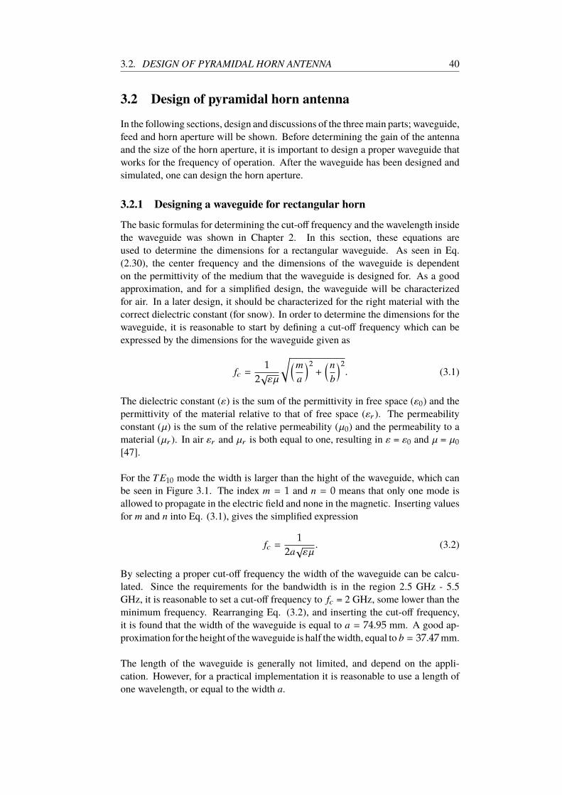
3.2. DESIGN OF PYRAMIDAL HORN ANTENNA 40
3.2 Design of pyramidal horn antenna
In the following sections, design and discussions of the three main parts; waveguide,
feed and horn aperture will be shown. Before determining the gain of the antenna
and the size of the horn aperture, it is important to design a proper waveguide that
works for the frequency of operation. After the waveguide has been designed and
simulated, one can design the horn aperture.
3.2.1 Designing a waveguide for rectangular horn
The basic formulas for determining the cut-off frequency and the wavelength inside
the waveguide was shown in Chapter 2. In this section, these equations are
used to determine the dimensions for a rectangular waveguide. As seen in Eq.
(2.30), the center frequency and the dimensions of the waveguide is dependent
on the permittivity of the medium that the waveguide is designed for. As a good
approximation, and for a simplified design, the waveguide will be characterized
for air. In a later design, it should be characterized for the right material with the
correct dielectric constant (for snow). In order to determine the dimensions for the
waveguide, it is reasonable to start by defining a cut-off frequency which can be
expressed by the dimensions for the waveguide given as
fc =1
2√εµ
√
(m
a
)2
+
(n
b
)2
. (3.1)
The dielectric constant (ε) is the sum of the permittivity in free space (ε0) and the
permittivity of the material relative to that of free space (εr ). The permeability
constant (µ) is the sum of the relative permeability (µ0) and the permeability to a
material (µr ). In air εr and µr is both equal to one, resulting in ε = ε0 and µ = µ0
[47].
For the TE10 mode the width is larger than the hight of the waveguide, which can
be seen in Figure 3.1. The index m = 1 and n = 0 means that only one mode is
allowed to propagate in the electric field and none in the magnetic. Inserting values
for m and n into Eq. (3.1), gives the simplified expression
fc =1
2a√εµ
. (3.2)
By selecting a proper cut-off frequency the width of the waveguide can be calcu-
lated. Since the requirements for the bandwidth is in the region 2.5 GHz - 5.5
GHz, it is reasonable to set a cut-off frequency to fc = 2 GHz, some lower than the
minimum frequency. Rearranging Eq. (3.2), and inserting the cut-off frequency,
it is found that the width of the waveguide is equal to a = 74.95 mm. A good ap-
proximation for the height of the waveguide is half the width, equal to b = 37.47 mm.
The length of the waveguide is generally not limited, and depend on the appli-
cation. However, for a practical implementation it is reasonable to use a length of
one wavelength, or equal to the width a.

41 CHAPTER 3. DESIGN AND ANALYSIS
b
λg/4
λ0/4
(a)
b
a
(b)
Figure 3.1: Standard waveguide feed. (a) cross section of waveguide side and, (b)
cross section of waveguide front.
The cut-off wavelength can be expressed by the formula
λc =2
√
(
ma
)2+
(
nb
)2. (3.3)
Inserting the values into the expression, gives an cut-off wavelength equal to
λc = 150mm.
Recalling the equations for the guided wavelength from Chapter 2
λg =λ0
√
1 −( fcf
)2, (3.4)
and inserting the wavelength in free space (λ0 = 75 mm), the cut-off frequency
(2 GHz) and the center frequency (4 GHz), gives an guided wavelength of
λg = 86.6mm [47].
3.2.2 Feeding a rectangular waveguide
Feeding a waveguide is traditionally accomplished by using a coaxial probe going
through the waveguide wall and into the inside of the waveguide, as can be seen in
Figure 3.1 [48].
The length of the probe and the distance between the probe and the cavity is
normally λ0/4 and λg/4, respectively, where λ0 is the wavelength at 4 GHz and λgis the guided wavelength. Equations for calculating the dimensions for the coaxial
cable has been given in Chapter 2. A handful of softwares and online tools exist
for calculating dimensions of coaxial cables, transmission lines and waveguides. In
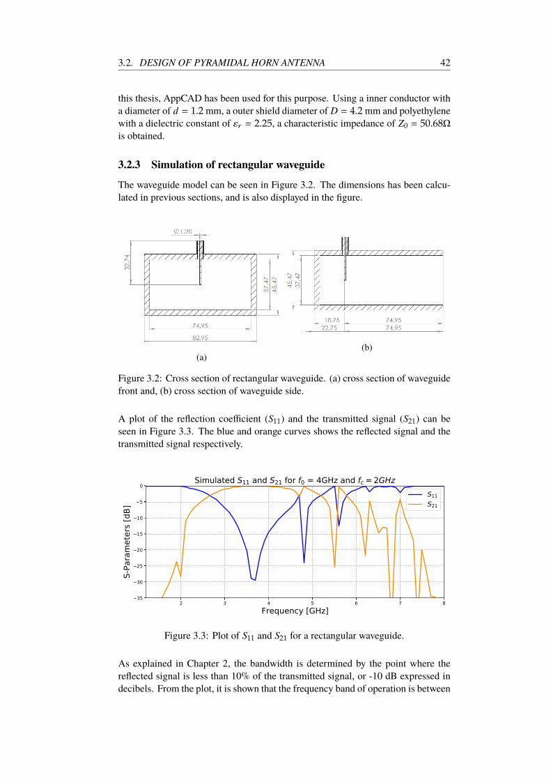
3.2. DESIGN OF PYRAMIDAL HORN ANTENNA 42
this thesis, AppCAD has been used for this purpose. Using a inner conductor with
a diameter of d = 1.2 mm, a outer shield diameter of D = 4.2 mm and polyethylene
with a dielectric constant of εr = 2.25, a characteristic impedance of Z0 = 50.68Ω
is obtained.
3.2.3 Simulation of rectangular waveguide
The waveguide model can be seen in Figure 3.2. The dimensions has been calcu-
lated in previous sections, and is also displayed in the figure.
(a)(b)
Figure 3.2: Cross section of rectangular waveguide. (a) cross section of waveguide
front and, (b) cross section of waveguide side.
A plot of the reflection coefficient (S11) and the transmitted signal (S21) can be
seen in Figure 3.3. The blue and orange curves shows the reflected signal and the
transmitted signal respectively.
2 3 4 5 6 7 8Frequency [GHz]
35
30
25
20
15
10
5
0
S-Pa
ram
eter
s [dB
]
Simulated S11 and S21 for f0 = 4GHz and fc = 2GHzS11S21
Figure 3.3: Plot of S11 and S21 for a rectangular waveguide.
As explained in Chapter 2, the bandwidth is determined by the point where the
reflected signal is less than 10% of the transmitted signal, or -10 dB expressed in
decibels. From the plot, it is shown that the frequency band of operation is between
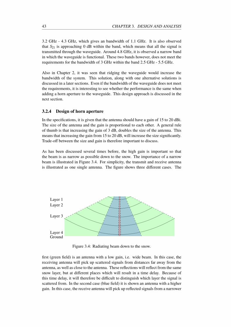
43 CHAPTER 3. DESIGN AND ANALYSIS
3.2 GHz - 4.3 GHz, which gives an bandwidth of 1.1 GHz. It is also observed
that S21 is approaching 0 dB within the band, which means that all the signal is
transmitted through the waveguide. Around 4.8 GHz, it is observed a narrow band
in which the waveguide is functional. These two bands however, does not meet the
requirements for the bandwidth of 3 GHz within the band 2.5 GHz - 5.5 GHz.
Also in Chapter 2, it was seen that ridging the waveguide would increase the
bandwidth of the system. This solution, along with one alternative solutions is
discussed in a later sections. Even if the bandwidth of the waveguide does not meet
the requirements, it is interesting to see whether the performance is the same when
adding a horn aperture to the waveguide. This design approach is discussed in the
next section.
3.2.4 Design of horn aperture
In the specifications, it is given that the antenna should have a gain of 15 to 20 dBi.
The size of the antenna and the gain is proportional to each other. A general rule
of thumb is that increasing the gain of 3 dB, doubles the size of the antenna. This
means that increasing the gain from 15 to 20 dB, will increase the size significantly.
Trade-off between the size and gain is therefore important to discuss.
As has been discussed several times before, the high gain is important so that
the beam is as narrow as possible down to the snow. The importance of a narrow
beam is illustrated in Figure 3.4. For simplicity, the transmit and receive antenna
is illustrated as one single antenna. The figure shows three different cases. The
Layer 1
Layer 2
Layer 3
Layer 4Ground
Figure 3.4: Radiating beam down to the snow.
first (green field) is an antenna with a low gain, i.e. wide beam. In this case, the
receiving antenna will pick up scattered signals from distances far away from the
antenna, as well as close to the antenna. These reflections will reflect from the same
snow layer, but at different places which will result in a time delay. Because of
this time delay, it will therefore be difficult to distinguish which layer the signal is
scattered from. In the second case (blue field) it is shown an antenna with a higher
gain. In this case, the receive antenna will pick up reflected signals from a narrower
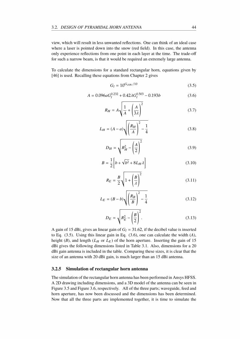
3.2. DESIGN OF PYRAMIDAL HORN ANTENNA 44
view, which will result in less unwanted reflections. One can think of an ideal case
where a laser is pointed down into the snow (red field). In this case, the antenna
only experience reflections from one point in each layer at the time. The trade-off
for such a narrow beam, is that it would be required an extremely large antenna.
To calculate the dimensions for a standard rectangular horn, equations given by
[46] is used. Recalling these equations from Chapter 2 gives
Gl = 10GdBi/10 (3.5)
A = 0.096aG0.232l + 0.42λG0.503
l − 0.193b (3.6)
RH = A
√
√
√
1
A+
(
A
3λ
)2
(3.7)
LH = (A− a)
√
√
√(
RH
A
)2
− 1
4(3.8)
DH =
√
√
√
R2H−
(
A
2
)2
(3.9)
B =1
2
[
b+√
b2+ 8LHλ
]
(3.10)
RE =B
2
√
√
√
1 +
(
B
λ
)2
(3.11)
LE = (B − b)
√
√
√(
RB
B
)2
− 1
4(3.12)
DE =
√
√
√
R2E−
(
B
2
)2
. (3.13)
A gain of 15 dBi, gives an linear gain of Gl = 31.62, if the decibel value is inserted
to Eq. (3.5). Using this linear gain in Eq. (3.6), one can calculate the width (A),
height (B), and length (LH or LE ) of the horn aperture. Inserting the gain of 15
dBi gives the following dimensions listed in Table 3.1. Also, dimensions for a 20
dBi gain antenna is included in the table. Comparing these sizes, it is clear that the
size of an antenna with 20 dBi gain, is much larger than an 15 dBi antenna.
3.2.5 Simulation of rectangular horn antenna
The simulation of the rectangular horn antenna has been performed in Ansys HFSS.
A 2D drawing including dimensions, and a 3D model of the antenna can be seen in
Figure 3.5 and Figure 3.6, respectively. All of the three parts; waveguide, feed and
horn aperture, has now been discussed and the dimensions has been determined.
Now that all the three parts are implemented together, it is time to simulate the
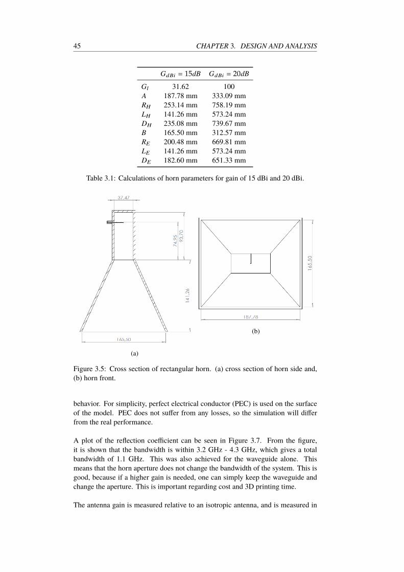
45 CHAPTER 3. DESIGN AND ANALYSIS
GdBi = 15dB GdBi = 20dB
Gl 31.62 100
A 187.78 mm 333.09 mm
RH 253.14 mm 758.19 mm
LH 141.26 mm 573.24 mm
DH 235.08 mm 739.67 mm
B 165.50 mm 312.57 mm
RE 200.48 mm 669.81 mm
LE 141.26 mm 573.24 mm
DE 182.60 mm 651.33 mm
Table 3.1: Calculations of horn parameters for gain of 15 dBi and 20 dBi.
(a)
(b)
Figure 3.5: Cross section of rectangular horn. (a) cross section of horn side and,
(b) horn front.
behavior. For simplicity, perfect electrical conductor (PEC) is used on the surface
of the model. PEC does not suffer from any losses, so the simulation will differ
from the real performance.
A plot of the reflection coefficient can be seen in Figure 3.7. From the figure,
it is shown that the bandwidth is within 3.2 GHz - 4.3 GHz, which gives a total
bandwidth of 1.1 GHz. This was also achieved for the waveguide alone. This
means that the horn aperture does not change the bandwidth of the system. This is
good, because if a higher gain is needed, one can simply keep the waveguide and
change the aperture. This is important regarding cost and 3D printing time.
The antenna gain is measured relative to an isotropic antenna, and is measured in
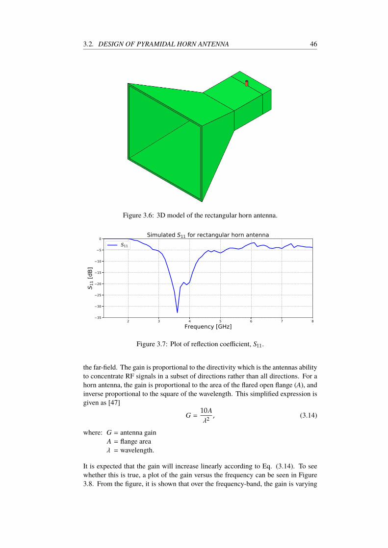
3.2. DESIGN OF PYRAMIDAL HORN ANTENNA 46
Figure 3.6: 3D model of the rectangular horn antenna.
2 3 4 5 6 7 8Frequency [GHz]
35
30
25
20
15
10
5
0
S 11 [
dB]
Simulated S11 for rectangular horn antennaS11
Figure 3.7: Plot of reflection coefficient, S11.
the far-field. The gain is proportional to the directivity which is the antennas ability
to concentrate RF signals in a subset of directions rather than all directions. For a
horn antenna, the gain is proportional to the area of the flared open flange (A), and
inverse proportional to the square of the wavelength. This simplified expression is
given as [47]
G =10A
λ2, (3.14)
where: G = antenna gain
A = flange area
λ = wavelength.
It is expected that the gain will increase linearly according to Eq. (3.14). To see
whether this is true, a plot of the gain versus the frequency can be seen in Figure
3.8. From the figure, it is shown that over the frequency-band, the gain is varying
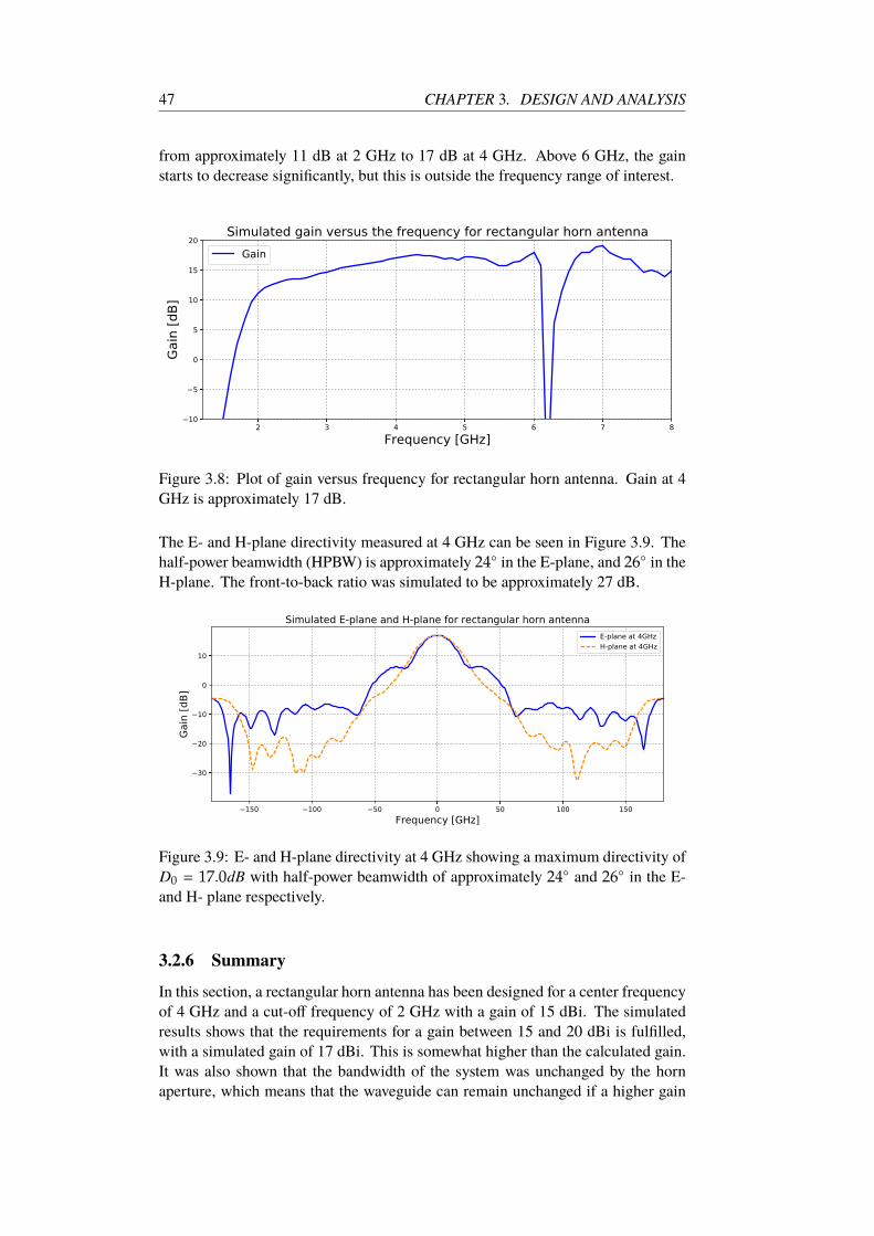
47 CHAPTER 3. DESIGN AND ANALYSIS
from approximately 11 dB at 2 GHz to 17 dB at 4 GHz. Above 6 GHz, the gain
starts to decrease significantly, but this is outside the frequency range of interest.
2 3 4 5 6 7 8Frequency [GHz]
10
5
0
5
10
15
20
Gain
[dB]
Simulated gain versus the frequency for rectangular horn antennaGain
Figure 3.8: Plot of gain versus frequency for rectangular horn antenna. Gain at 4
GHz is approximately 17 dB.
The E- and H-plane directivity measured at 4 GHz can be seen in Figure 3.9. The
half-power beamwidth (HPBW) is approximately 24 in the E-plane, and 26 in the
H-plane. The front-to-back ratio was simulated to be approximately 27 dB.
150 100 50 0 50 100 150Frequency [GHz]
30
20
10
0
10
Gain
[dB]
Simulated E-plane and H-plane for rectangular horn antennaE-plane at 4GHzH-plane at 4GHz
Figure 3.9: E- and H-plane directivity at 4 GHz showing a maximum directivity of
D0 = 17.0dB with half-power beamwidth of approximately 24 and 26 in the E-
and H- plane respectively.
3.2.6 Summary
In this section, a rectangular horn antenna has been designed for a center frequency
of 4 GHz and a cut-off frequency of 2 GHz with a gain of 15 dBi. The simulated
results shows that the requirements for a gain between 15 and 20 dBi is fulfilled,
with a simulated gain of 17 dBi. This is somewhat higher than the calculated gain.
It was also shown that the bandwidth of the system was unchanged by the horn
aperture, which means that the waveguide can remain unchanged if a higher gain

3.2. DESIGN OF PYRAMIDAL HORN ANTENNA 48
is needed. However, the bandwidth does not meet the system requirements of 3
GHz bandwidth between 2.5 GHz to 5.5 GHz. Other techniques needs to be used
in order to get a wider bandwidth. This is discussed in the next section.
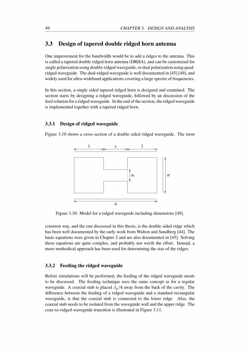
49 CHAPTER 3. DESIGN AND ANALYSIS
3.3 Design of tapered double ridged horn antenna
One improvement for the bandwidth would be to add a ridges to the antenna. This
is called a tapered double ridged horn antenna (DRHA), and can be customized for
single polarization using double-ridged waveguide, or dual polarization using quad-
ridged waveguide. The dual-ridged waveguide is well documented in [45] [49], and
widely used for ultra-wideband applications covering a large specter of frequencies.
In this section, a single sided tapered ridged horn is designed and examined. The
section starts by designing a ridged waveguide, followed by an discussion of the
feed solution for a ridged waveguide. In the end of the section, the ridged waveguide
is implemented together with a tapered ridged horn.
3.3.1 Design of ridged waveguide
Figure 3.10 shows a cross section of a double sided ridged waveguide. The most
b
a
l ls
d
Figure 3.10: Model for a ridged waveguide including dimensions [49].
common way, and the one discussed in this thesis, is the double sided ridge which
has been well documented by the early work from Walton and Sundberg [44]. The
basic equations were given in Chapter 2 and are also documented in [45]. Solving
these equations are quite complex, and probably not worth the effort. Instead, a
more methodical approach has been used for determining the size of the ridges.
3.3.2 Feeding the ridged waveguide
Before simulations will be performed, the feeding of the ridged waveguide needs
to be discussed. The feeding technique uses the same concept as for a regular
waveguide. A coaxial stub is placed λg/4 away from the back of the cavity. The
difference between the feeding of a ridged waveguide and a standard rectangular
waveguide, is that the coaxial stub is connected to the lower ridge. Also, the
coaxial stub needs to be isolated from the waveguide wall and the upper ridge. The
coax-to-ridged-waveguide transition is illustrated in Figure 3.11.

3.3. DESIGN OF TAPERED DOUBLE RIDGED HORN ANTENNA 50
Figure 3.11: Cross section of coax to ridged waveguide transition. Coax stub is
isolated by a dielectric material from the upper ridge, and is connected to the lower
ridge [44].
3.3.3 Simulation of ridged waveguide
The ridged waveguide has the same dimensions as calculated in section 3.2.1 De-
sign of waveguide for rectangular horn. The critical parameters are mainly the gap
and the width of the ridges. Simulations has been carried out in order to optimize
these two parameters.
It was found that a gap equal to 1 mm and a ridge-width equal to 10 mm gave
the best performance. A plot of S11 is shown in Figure 3.12. The new bandwidth
2 3 4 5 6 7 8Frequency [GHz]
45
40
35
30
25
20
15
10
5
0
S 11 [
dB]
Simulated S11 for double ridged waveguideS11
Figure 3.12: Plot of S11 for double ridged waveguide with a gap of 1 mm and a
ridge-width of 10 mm.
for the waveguide is in the region between approximately 700 MHz to 4.9 GHz,
giving a total bandwidth of 4.2 GHz. Comparing this result with the one in Figure
3.3 for the rectangular waveguide, it is clear that by adding ridges increases the
bandwidth. However, this does not meet the system requirements for a bandwidth
between 2.5 GHz and 5.5 GHz. From the figure it is shown that the upper frequency
is almost unchanged, while the lower frequency is shifted down by more than 3
GHz. Therefore, one possible solution for obtaining a bandwidth covering the entire
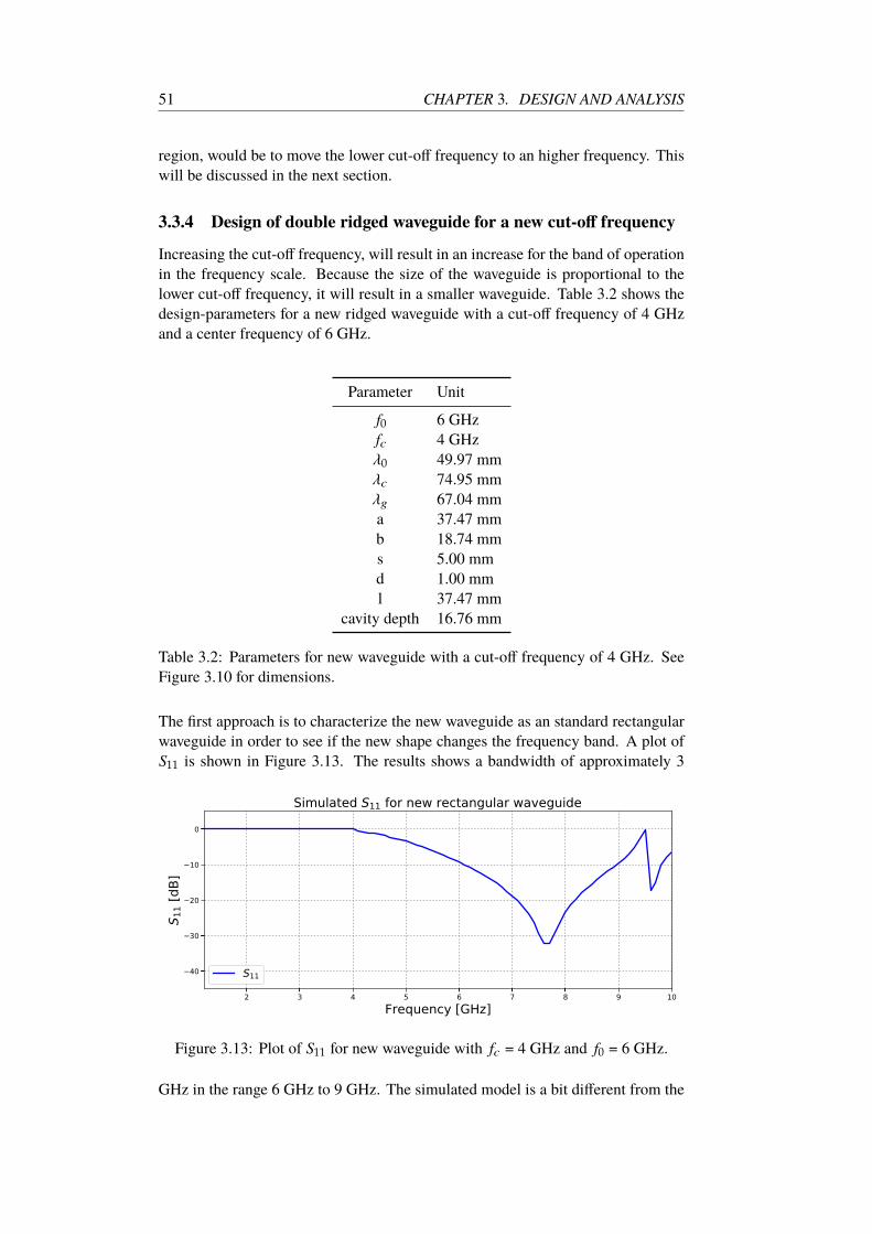
51 CHAPTER 3. DESIGN AND ANALYSIS
region, would be to move the lower cut-off frequency to an higher frequency. This
will be discussed in the next section.
3.3.4 Design of double ridged waveguide for a new cut-off frequency
Increasing the cut-off frequency, will result in an increase for the band of operation
in the frequency scale. Because the size of the waveguide is proportional to the
lower cut-off frequency, it will result in a smaller waveguide. Table 3.2 shows the
design-parameters for a new ridged waveguide with a cut-off frequency of 4 GHz
and a center frequency of 6 GHz.
Parameter Unit
f0 6 GHz
fc 4 GHz
λ0 49.97 mm
λc 74.95 mm
λg 67.04 mm
a 37.47 mm
b 18.74 mm
s 5.00 mm
d 1.00 mm
l 37.47 mm
cavity depth 16.76 mm
Table 3.2: Parameters for new waveguide with a cut-off frequency of 4 GHz. See
Figure 3.10 for dimensions.
The first approach is to characterize the new waveguide as an standard rectangular
waveguide in order to see if the new shape changes the frequency band. A plot of
S11 is shown in Figure 3.13. The results shows a bandwidth of approximately 3
2 3 4 5 6 7 8 9 10Frequency [GHz]
40
30
20
10
0
S 11 [
dB]
Simulated S11 for new rectangular waveguide
S11
Figure 3.13: Plot of S11 for new waveguide with fc = 4 GHz and f0 = 6 GHz.
GHz in the range 6 GHz to 9 GHz. The simulated model is a bit different from the
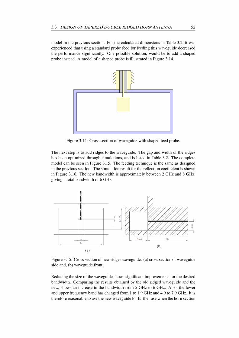
3.3. DESIGN OF TAPERED DOUBLE RIDGED HORN ANTENNA 52
model in the previous section. For the calculated dimensions in Table 3.2, it was
experienced that using a standard probe feed for feeding this waveguide decreased
the performance significantly. One possible solution, would be to add a shaped
probe instead. A model of a shaped probe is illustrated in Figure 3.14.
Figure 3.14: Cross section of waveguide with shaped feed probe.
The next step is to add ridges to the waveguide. The gap and width of the ridges
has been optimized through simulations, and is listed in Table 3.2. The complete
model can be seen in Figure 3.15. The feeding technique is the same as designed
in the previous section. The simulation result for the reflection coefficient is shown
in Figure 3.16. The new bandwidth is approximately between 2 GHz and 8 GHz,
giving a total bandwidth of 6 GHz.
(a)(b)
Figure 3.15: Cross section of new ridges waveguide. (a) cross section of waveguide
side and, (b) waveguide front.
Reducing the size of the waveguide shows significant improvements for the desired
bandwidth. Comparing the results obtained by the old ridged waveguide and the
new, shows an increase in the bandwidth from 5 GHz to 6 GHz. Also, the lower
and upper frequency band has changed from 1 to 1.9 GHz and 4.9 to 7.9 GHz. It is
therefore reasonable to use the new waveguide for further use when the horn section
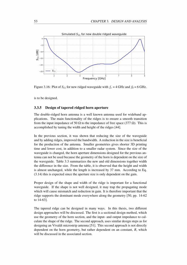
53 CHAPTER 3. DESIGN AND ANALYSIS
2 3 4 5 6 7 8 9Frequency [GHz]
25
20
15
10
5
0S 1
1 [dB
]Simulated S11 for new double ridged waveguide
S11
Figure 3.16: Plot of S11 for new ridged waveguide with fc = 4 GHz and f0 = 6 GHz.
is to be designed.
3.3.5 Design of tapered ridged horn aperture
The double-ridged horn antenna is a well known antenna used for wideband ap-
plications. The main functionality of the ridges is to ensure a smooth transition
from the input impedance of 50 Ω to the impedance of free space (377 Ω). This is
accomplished by tuning the width and height of the ridges [44].
In the previous section, it was shown that reducing the size of the waveguide
and by adding ridges, improved the bandwidth. A reduction in the size is beneficial
for the production of the antenna. Smaller geometries gives shorter 3D printing
time and lower cost, in addition to a smaller radar system. Since the size of the
waveguide is changed, the horn aperture dimensions designed for the previous an-
tenna can not be used because the geometry of the horn is dependent on the size of
the waveguide. Table 3.3 summarizes the new and old dimensions together width
the difference in the size. From the table, it is observed that the height and width
is almost unchanged, while the length is increased by 37 mm. According to Eq.
(3.14) this is expected since the aperture size is only dependent on the gain.
Proper design of the shape and width of the ridge is important for a functional
waveguide. If the shape is not well designed, it may trap the propagating mode
which will cause mismatch and reduction in gain. It is therefore important that the
ridge supports the dominant mode everywhere along the geometry [50, pp. 14-62
to 14-63].
The tapered ridge can be designed in many ways. In this thesis, two different
design approaches will be discussed. The first is a sectional design method, which
use the geometry of the horn section, and the input- and output impedance to cal-
culate the shape of the ridge. The second approach, uses similar design steps as for
designing an Vivaldi microstrip antenna [51]. This second approach is not directly
dependent on the horn geometry, but rather dependent on an constant, R, which
will be discussed in the associated section.
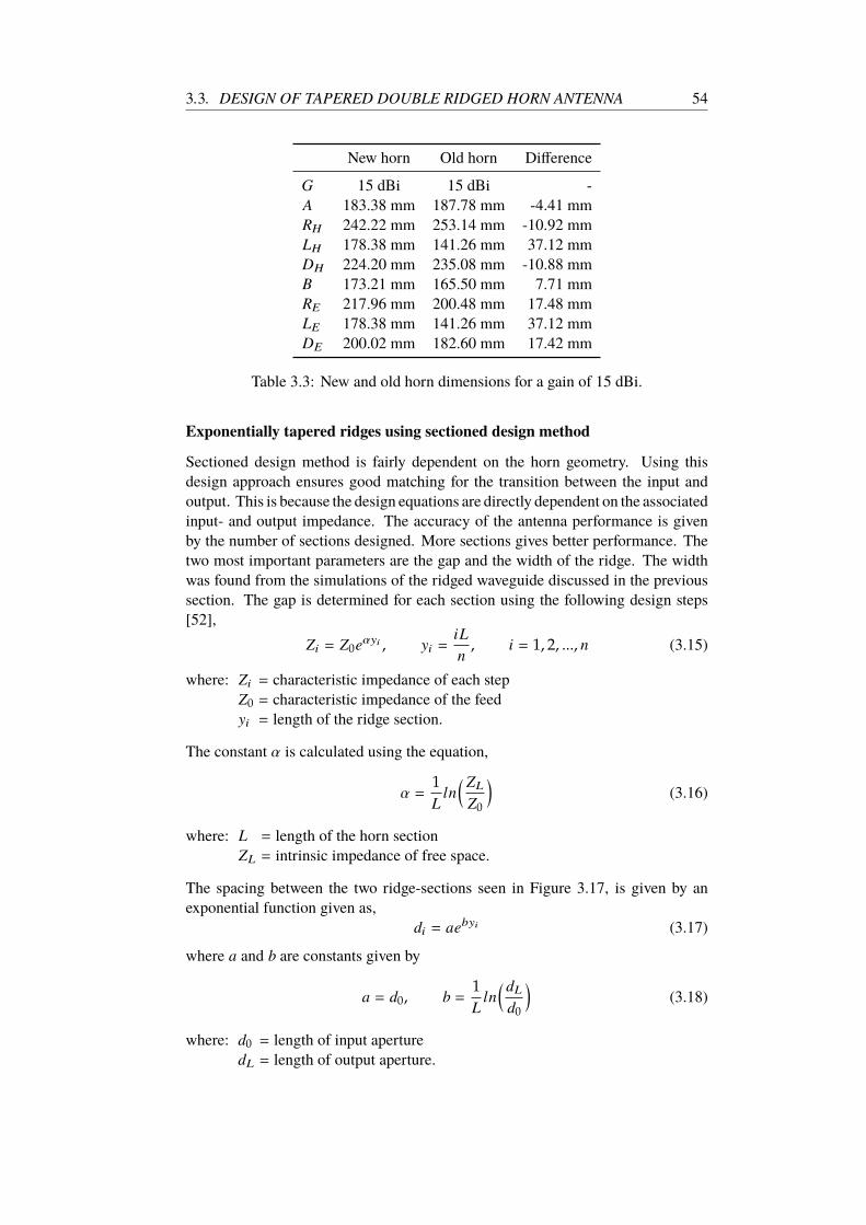
3.3. DESIGN OF TAPERED DOUBLE RIDGED HORN ANTENNA 54
New horn Old horn Difference
G 15 dBi 15 dBi -
A 183.38 mm 187.78 mm -4.41 mm
RH 242.22 mm 253.14 mm -10.92 mm
LH 178.38 mm 141.26 mm 37.12 mm
DH 224.20 mm 235.08 mm -10.88 mm
B 173.21 mm 165.50 mm 7.71 mm
RE 217.96 mm 200.48 mm 17.48 mm
LE 178.38 mm 141.26 mm 37.12 mm
DE 200.02 mm 182.60 mm 17.42 mm
Table 3.3: New and old horn dimensions for a gain of 15 dBi.
Exponentially tapered ridges using sectioned design method
Sectioned design method is fairly dependent on the horn geometry. Using this
design approach ensures good matching for the transition between the input and
output. This is because the design equations are directly dependent on the associated
input- and output impedance. The accuracy of the antenna performance is given
by the number of sections designed. More sections gives better performance. The
two most important parameters are the gap and the width of the ridge. The width
was found from the simulations of the ridged waveguide discussed in the previous
section. The gap is determined for each section using the following design steps
[52],
Zi = Z0eαyi , yi =iL
n, i = 1, 2, ..., n (3.15)
where: Zi = characteristic impedance of each step
Z0 = characteristic impedance of the feed
yi = length of the ridge section.
The constant α is calculated using the equation,
α =1
Lln
( ZL
Z0
)
(3.16)
where: L = length of the horn section
ZL = intrinsic impedance of free space.
The spacing between the two ridge-sections seen in Figure 3.17, is given by an
exponential function given as,
di = aebyi (3.17)
where a and b are constants given by
a = d0, b =1
Lln
( dL
d0
)
(3.18)
where: d0 = length of input aperture
dL = length of output aperture.
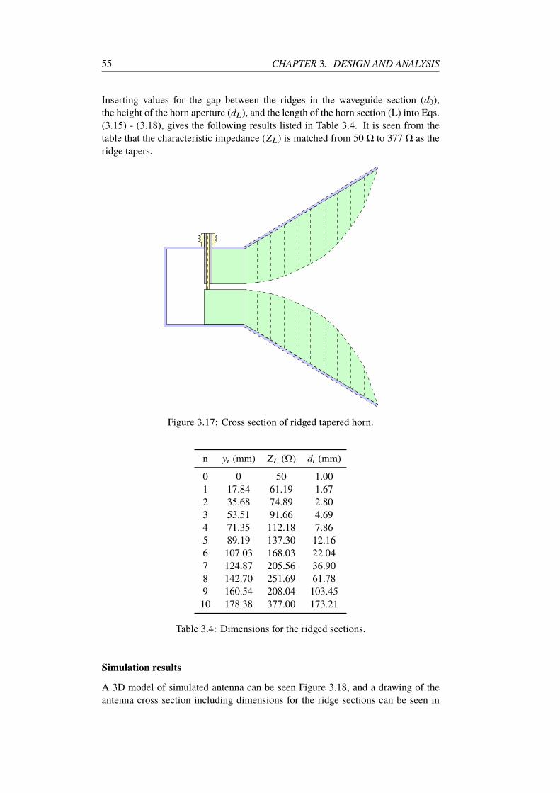
55 CHAPTER 3. DESIGN AND ANALYSIS
Inserting values for the gap between the ridges in the waveguide section (d0),
the height of the horn aperture (dL), and the length of the horn section (L) into Eqs.
(3.15) - (3.18), gives the following results listed in Table 3.4. It is seen from the
table that the characteristic impedance (ZL) is matched from 50 Ω to 377 Ω as the
ridge tapers.
Figure 3.17: Cross section of ridged tapered horn.
n yi (mm) ZL (Ω) di (mm)
0 0 50 1.00
1 17.84 61.19 1.67
2 35.68 74.89 2.80
3 53.51 91.66 4.69
4 71.35 112.18 7.86
5 89.19 137.30 12.16
6 107.03 168.03 22.04
7 124.87 205.56 36.90
8 142.70 251.69 61.78
9 160.54 208.04 103.45
10 178.38 377.00 173.21
Table 3.4: Dimensions for the ridged sections.
Simulation results
A 3D model of simulated antenna can be seen Figure 3.18, and a drawing of the
antenna cross section including dimensions for the ridge sections can be seen in
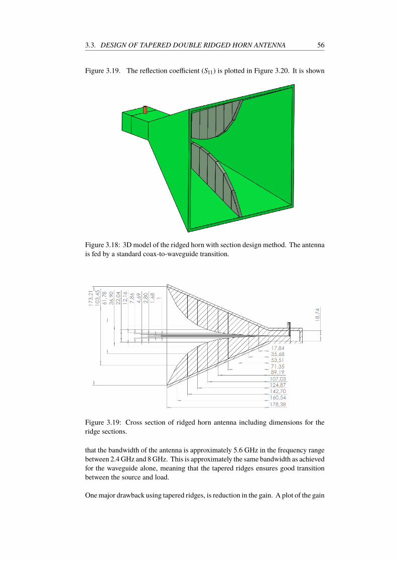
3.3. DESIGN OF TAPERED DOUBLE RIDGED HORN ANTENNA 56
Figure 3.19. The reflection coefficient (S11) is plotted in Figure 3.20. It is shown
Figure 3.18: 3D model of the ridged horn with section design method. The antenna
is fed by a standard coax-to-waveguide transition.
Figure 3.19: Cross section of ridged horn antenna including dimensions for the
ridge sections.
that the bandwidth of the antenna is approximately 5.6 GHz in the frequency range
between 2.4 GHz and 8 GHz. This is approximately the same bandwidth as achieved
for the waveguide alone, meaning that the tapered ridges ensures good transition
between the source and load.
One major drawback using tapered ridges, is reduction in the gain. A plot of the gain
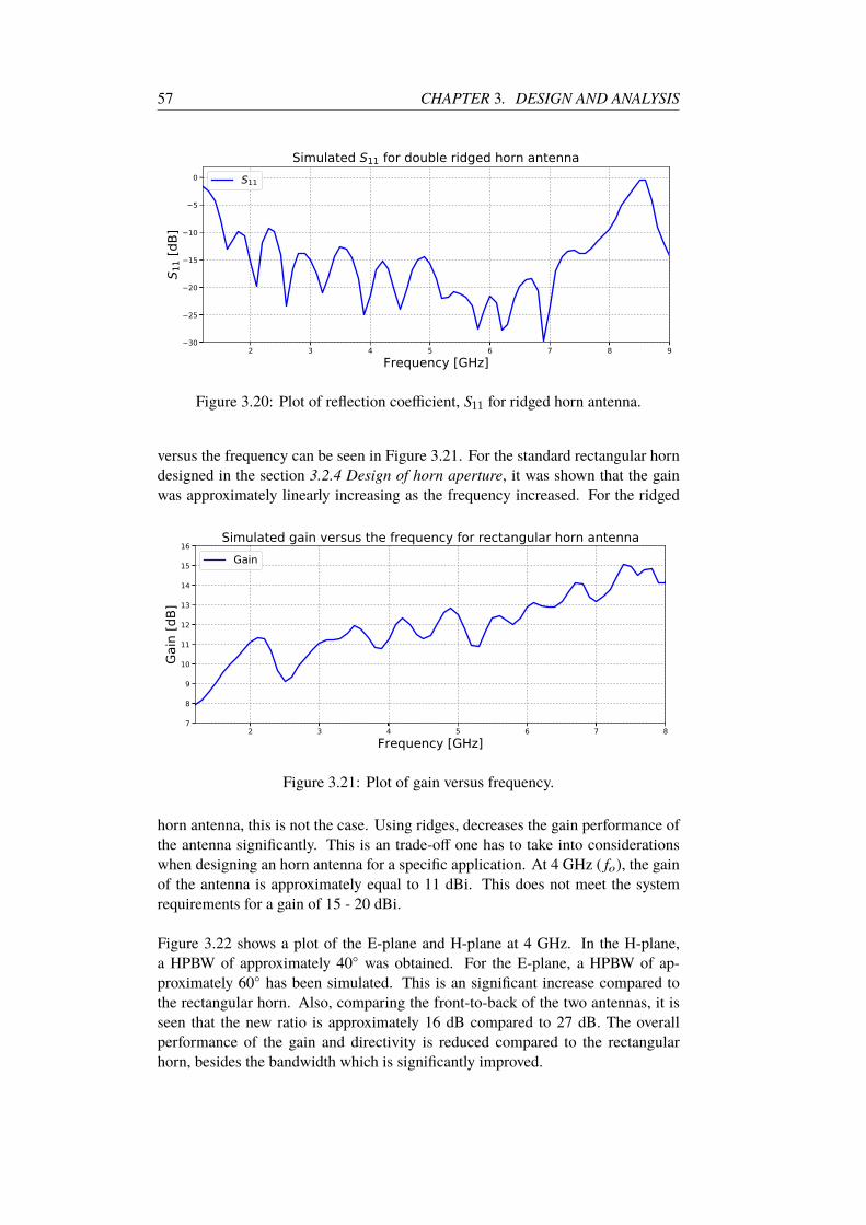
57 CHAPTER 3. DESIGN AND ANALYSIS
2 3 4 5 6 7 8 9Frequency [GHz]
30
25
20
15
10
5
0S 1
1 [dB
]Simulated S11 for double ridged horn antenna
S11
Figure 3.20: Plot of reflection coefficient, S11 for ridged horn antenna.
versus the frequency can be seen in Figure 3.21. For the standard rectangular horn
designed in the section 3.2.4 Design of horn aperture, it was shown that the gain
was approximately linearly increasing as the frequency increased. For the ridged
2 3 4 5 6 7 8Frequency [GHz]
7
8
9
10
11
12
13
14
15
16
Gain
[dB]
Simulated gain versus the frequency for rectangular horn antennaGain
Figure 3.21: Plot of gain versus frequency.
horn antenna, this is not the case. Using ridges, decreases the gain performance of
the antenna significantly. This is an trade-off one has to take into considerations
when designing an horn antenna for a specific application. At 4 GHz ( fo), the gain
of the antenna is approximately equal to 11 dBi. This does not meet the system
requirements for a gain of 15 - 20 dBi.
Figure 3.22 shows a plot of the E-plane and H-plane at 4 GHz. In the H-plane,
a HPBW of approximately 40 was obtained. For the E-plane, a HPBW of ap-
proximately 60 has been simulated. This is an significant increase compared to
the rectangular horn. Also, comparing the front-to-back of the two antennas, it is
seen that the new ratio is approximately 16 dB compared to 27 dB. The overall
performance of the gain and directivity is reduced compared to the rectangular
horn, besides the bandwidth which is significantly improved.
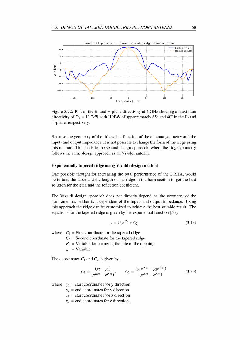
3.3. DESIGN OF TAPERED DOUBLE RIDGED HORN ANTENNA 58
150 100 50 0 50 100 150Frequency [GHz]
20
15
10
5
0
5
10
Gain
[dB]
Simulated E-plane and H-plane for double ridged horn antennaE-plane at 4GHzH-plane at 4GHz
Figure 3.22: Plot of the E- and H-plane directivity at 4 GHz showing a maximum
directivity of D0 = 11.2dB with HPBW of approximately 65 and 40 in the E- and
H-plane, respectively.
Because the geometry of the ridges is a function of the antenna geometry and the
input- and output impedance, it is not possible to change the form of the ridge using
this method. This leads to the second design approach, where the ridge geometry
follows the same design approach as an Vivaldi antenna.
Exponentially tapered ridge using Vivaldi design method
One possible thought for increasing the total performance of the DRHA, would
be to tune the taper and the length of the ridge in the horn section to get the best
solution for the gain and the reflection coefficient.
The Vivaldi design approach does not directly depend on the geometry of the
horn antenna, neither is it dependent of the input- and output impedance. Using
this approach the ridge can be customized to achieve the best suitable result. The
equations for the tapered ridge is given by the exponential function [53],
y = C1eRz +C2 (3.19)
where: C1 = First coordinate for the tapered ridge
C2 = Second coordinate for the tapered ridge
R = Variable for changing the rate of the opening
z = Variable.
The coordinates C1 and C2 is given by,
C1 =(y2 − y1)
(eRz2 − eRz1) , C2 =(y1eRz2 − y2eRz1)(eRz2 − eRz1) (3.20)
where: y1 = start coordinates for y direction
y2 = end coordinates for y direction
z1 = start coordinates for z direction
z2 = end coordinates for z direction.

59 CHAPTER 3. DESIGN AND ANALYSIS
The variable R controls the taper of the ridge, and increasing the R value gives an
steeper ridge. Selecting this parameter properly, is the greatest design challenge for
an properly designed ridge.
Simulation results
A plot of S11 for three different R values, are shown in Figure 3.23. The plot clearly
shows the effect of changing the variable. It is shown that for a R equal to 20 gives
an bandwidth of approximately 3.3 GHz in the range 4.5 GHz to 7.8 GHz, while
for an R equal to 60, the bandwidth is increased to about 5.7 GHz in the range 2.3
GHz to 8 GHz. In this case, the antenna fulfill the requirements for the bandwidth.
2 3 4 5 6 7 8Frequency [GHz]
30
25
20
15
10
5
0
S 11 [
dB]
Simulated S11 for three different values for RR = 60R = 40R = 20
Figure 3.23: Plot of reflection coefficient, S11 for ridged horn antenna with three
different R values.
Having a relatively steep ridge, ensures good bandwidth, but this will affect the gain
of the antenna. A plot of the gain versus frequency for the same values are shown
in Figure 3.26. As can be seen, the gain varies due to the changes in the ridge.
2 3 4 5 6 7 8Frequency [GHz]
6
8
10
12
14
16
18
Gain
[dB]
Simulated gain versus the frequency for three different values of RR = 60R = 40R = 20
Figure 3.24: Plot of gain versus frequency for three different R values.
The best gain is achieved when the bandwidth is poorest. At center-frequency (4

3.3. DESIGN OF TAPERED DOUBLE RIDGED HORN ANTENNA 60
GHz), the gain is about 13 dBi for R equal to 20 and about 8 dBi for R equal
to 60. Reduction in gain is common for double ridged horn antennas as multiple
modes are excited and the beamwidth broadens. This effect has been documented
by [54, pp. 365-372] and Figure 3.25 shows a plot of the gain for a quad-ridged
horn compared to smooth- and corrugated-wall horns.
Figure 3.25: Measured directivity of a circular quad-ridged horn compared to those
of smooth- and corrugated-wall horns. From [54].
Radiation pattern
The simulated radiation pattern for the E- and H-plane for R equal to 60, 40 and 20
at 4 GHz is shown in Figure 3.26. As previously explained, the highest directivity
is achieved when the R-value is lowest. The simulated maximum directivity for
this case, is at D0 = 12.8 dB, with a HPBW equal to 52 in the E-plane and 30
in the H-plane. For the two other R-values, it is observed that the directivity in
zenith is slightly degraded from the maximum directivity. As the R increases,
this degradation becomes greater. For R equal to 40, the maximum directivity is
measured to be D0 = 10.2 dB, with a HPBW equal to 54 in the E-plane, and 30 in
the H-plane. For R equal to 20, the measured maximum directivity is equal to D0
= 8.1 dB, and the HPBW equal to 56 and 30 in the E- and H-plane, respectively.
3.3.6 Summary
In this section, ridges has been added to the waveguide and horn section. It was
shown that the ridge lowered the cut-off frequency of the first dominant mode,
which lead to an reduction in the size of the waveguide. This is beneficial consid-
ering production time and the practical usage. Then, two different design methods
for adding ridges to the horn section was explained and simulated using HFSS. It
was shown that the ridges increased the bandwidth of the antenna compared to the
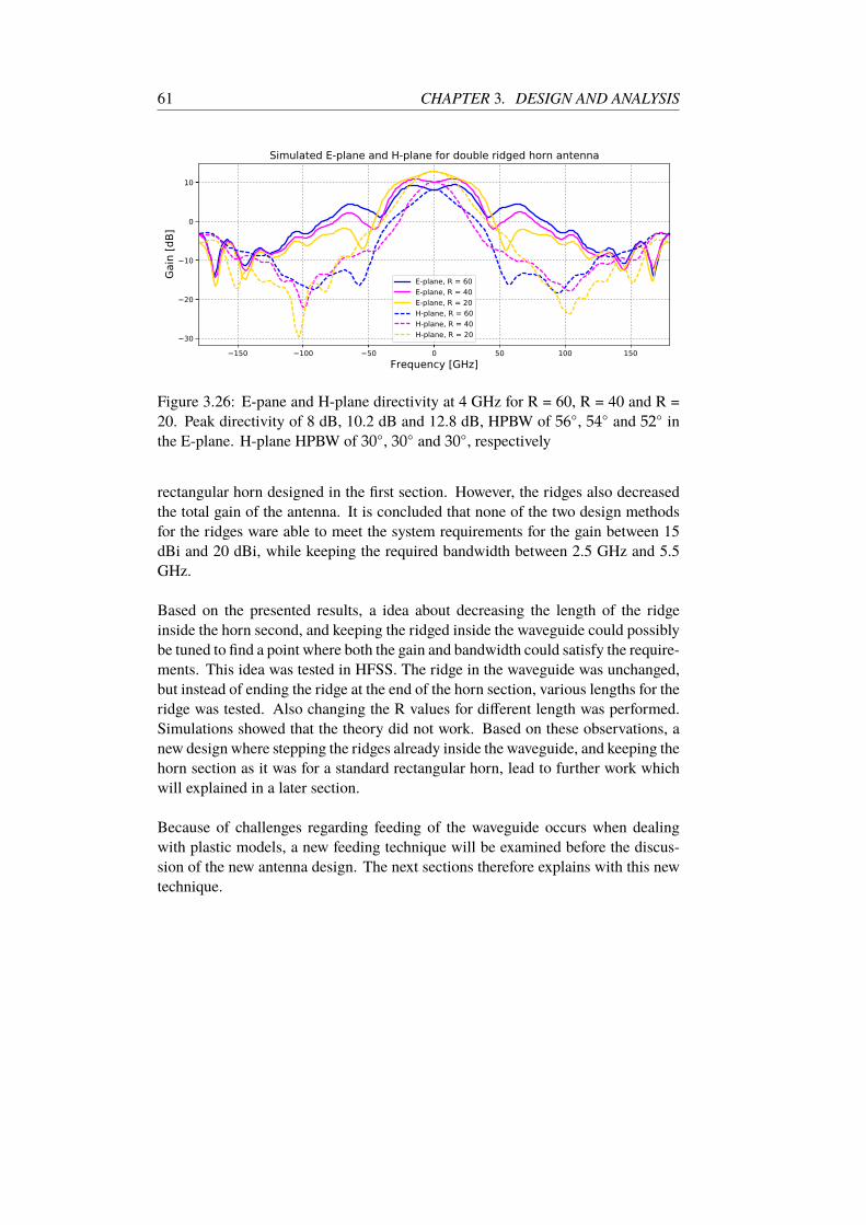
61 CHAPTER 3. DESIGN AND ANALYSIS
150 100 50 0 50 100 150Frequency [GHz]
30
20
10
0
10Ga
in [d
B]Simulated E-plane and H-plane for double ridged horn antenna
E-plane, R = 60E-plane, R = 40E-plane, R = 20H-plane, R = 60H-plane, R = 40H-plane, R = 20
Figure 3.26: E-pane and H-plane directivity at 4 GHz for R = 60, R = 40 and R =
20. Peak directivity of 8 dB, 10.2 dB and 12.8 dB, HPBW of 56, 54 and 52 in
the E-plane. H-plane HPBW of 30, 30 and 30, respectively
rectangular horn designed in the first section. However, the ridges also decreased
the total gain of the antenna. It is concluded that none of the two design methods
for the ridges ware able to meet the system requirements for the gain between 15
dBi and 20 dBi, while keeping the required bandwidth between 2.5 GHz and 5.5
GHz.
Based on the presented results, a idea about decreasing the length of the ridge
inside the horn second, and keeping the ridged inside the waveguide could possibly
be tuned to find a point where both the gain and bandwidth could satisfy the require-
ments. This idea was tested in HFSS. The ridge in the waveguide was unchanged,
but instead of ending the ridge at the end of the horn section, various lengths for the
ridge was tested. Also changing the R values for different length was performed.
Simulations showed that the theory did not work. Based on these observations, a
new design where stepping the ridges already inside the waveguide, and keeping the
horn section as it was for a standard rectangular horn, lead to further work which
will explained in a later section.
Because of challenges regarding feeding of the waveguide occurs when dealing
with plastic models, a new feeding technique will be examined before the discus-
sion of the new antenna design. The next sections therefore explains with this new
technique.
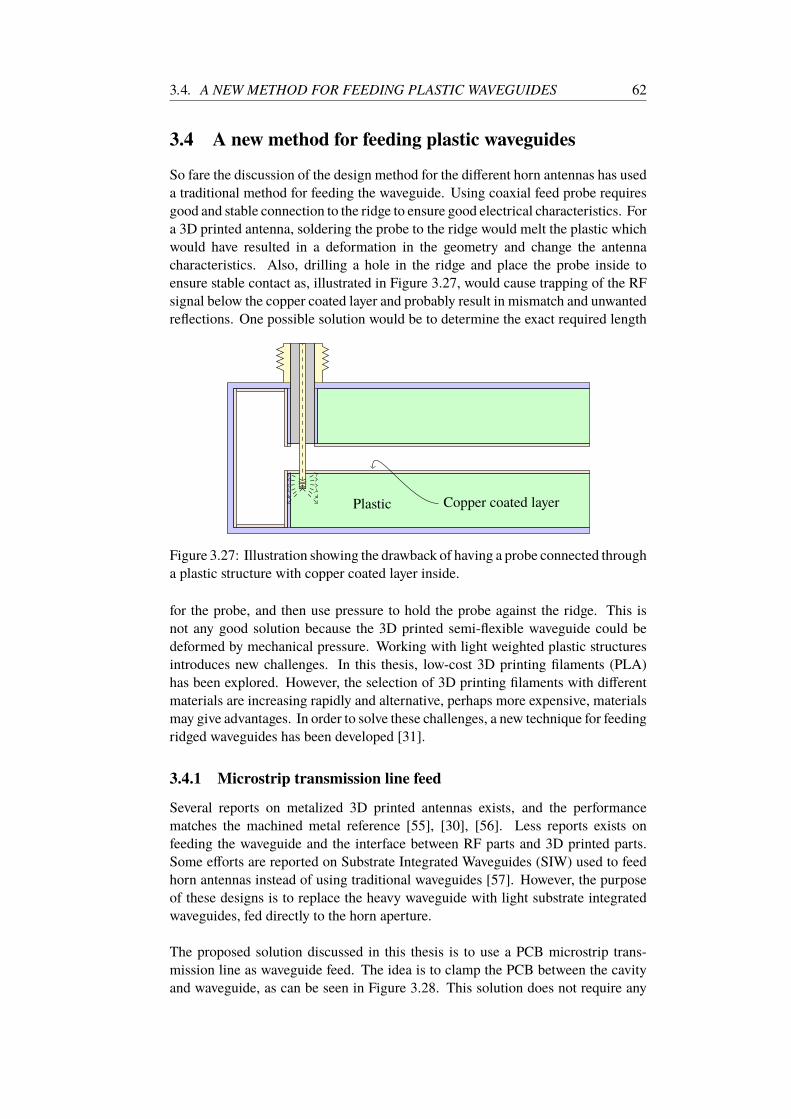
3.4. A NEW METHOD FOR FEEDING PLASTIC WAVEGUIDES 62
3.4 A new method for feeding plastic waveguides
So fare the discussion of the design method for the different horn antennas has used
a traditional method for feeding the waveguide. Using coaxial feed probe requires
good and stable connection to the ridge to ensure good electrical characteristics. For
a 3D printed antenna, soldering the probe to the ridge would melt the plastic which
would have resulted in a deformation in the geometry and change the antenna
characteristics. Also, drilling a hole in the ridge and place the probe inside to
ensure stable contact as, illustrated in Figure 3.27, would cause trapping of the RF
signal below the copper coated layer and probably result in mismatch and unwanted
reflections. One possible solution would be to determine the exact required length
Copper coated layerPlastic
Figure 3.27: Illustration showing the drawback of having a probe connected through
a plastic structure with copper coated layer inside.
for the probe, and then use pressure to hold the probe against the ridge. This is
not any good solution because the 3D printed semi-flexible waveguide could be
deformed by mechanical pressure. Working with light weighted plastic structures
introduces new challenges. In this thesis, low-cost 3D printing filaments (PLA)
has been explored. However, the selection of 3D printing filaments with different
materials are increasing rapidly and alternative, perhaps more expensive, materials
may give advantages. In order to solve these challenges, a new technique for feeding
ridged waveguides has been developed [31].
3.4.1 Microstrip transmission line feed
Several reports on metalized 3D printed antennas exists, and the performance
matches the machined metal reference [55], [30], [56]. Less reports exists on
feeding the waveguide and the interface between RF parts and 3D printed parts.
Some efforts are reported on Substrate Integrated Waveguides (SIW) used to feed
horn antennas instead of using traditional waveguides [57]. However, the purpose
of these designs is to replace the heavy waveguide with light substrate integrated
waveguides, fed directly to the horn aperture.
The proposed solution discussed in this thesis is to use a PCB microstrip trans-
mission line as waveguide feed. The idea is to clamp the PCB between the cavity
and waveguide, as can be seen in Figure 3.28. This solution does not require any
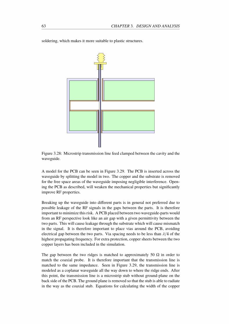
63 CHAPTER 3. DESIGN AND ANALYSIS
soldering, which makes it more suitable to plastic structures.
Figure 3.28: Microstrip transmission line feed clamped between the cavity and the
waveguide.
A model for the PCB can be seen in Figure 3.29. The PCB is inserted across the
waveguide by splitting the model in two. The copper and the substrate is removed
for the free space areas of the waveguide imposing negligible interference. Open-
ing the PCB as described, will weaken the mechanical properties but significantly
improve RF properties.
Breaking up the waveguide into different parts is in general not preferred due to
possible leakage of the RF signals in the gaps between the parts. It is therefore
important to minimize this risk. A PCB placed between two waveguide-parts would
from an RF perspective look like an air gap with a given permittivity between the
two parts. This will cause leakage through the substrate which will cause mismatch
in the signal. It is therefore important to place vias around the PCB, avoiding
electrical gap between the two parts. Via spacing needs to be less than λ/4 of the
highest propagating frequency. For extra protection, copper sheets between the two
copper layers has been included in the simulation.
The gap between the two ridges is matched to approximately 50 Ω in order to
match the coaxial probe. It is therefore important that the transmission line is
matched to the same impedance. Seen in Figure 3.29, the transmission line is
modeled as a coplanar waveguide all the way down to where the ridge ends. After
this point, the transmission line is a microstrip stub without ground-plane on the
back side of the PCB. The ground plane is removed so that the stub is able to radiate
in the way as the coaxial stub. Equations for calculating the width of the copper
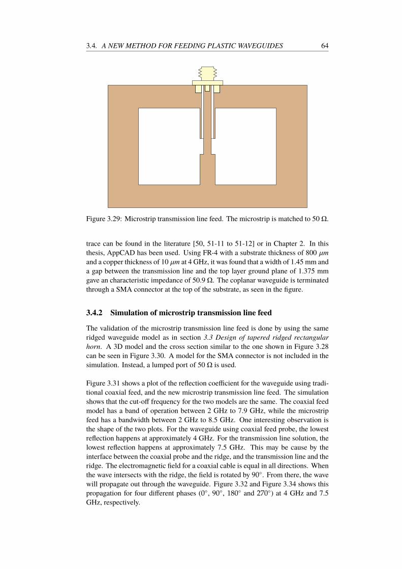
3.4. A NEW METHOD FOR FEEDING PLASTIC WAVEGUIDES 64
Figure 3.29: Microstrip transmission line feed. The microstrip is matched to 50 Ω.
trace can be found in the literature [50, 51-11 to 51-12] or in Chapter 2. In this
thesis, AppCAD has been used. Using FR-4 with a substrate thickness of 800 µm
and a copper thickness of 10 µm at 4 GHz, it was found that a width of 1.45 mm and
a gap between the transmission line and the top layer ground plane of 1.375 mm
gave an characteristic impedance of 50.9 Ω. The coplanar waveguide is terminated
through a SMA connector at the top of the substrate, as seen in the figure.
3.4.2 Simulation of microstrip transmission line feed
The validation of the microstrip transmission line feed is done by using the same
ridged waveguide model as in section 3.3 Design of tapered ridged rectangular
horn. A 3D model and the cross section similar to the one shown in Figure 3.28
can be seen in Figure 3.30. A model for the SMA connector is not included in the
simulation. Instead, a lumped port of 50 Ω is used.
Figure 3.31 shows a plot of the reflection coefficient for the waveguide using tradi-
tional coaxial feed, and the new microstrip transmission line feed. The simulation
shows that the cut-off frequency for the two models are the same. The coaxial feed
model has a band of operation between 2 GHz to 7.9 GHz, while the microstrip
feed has a bandwidth between 2 GHz to 8.5 GHz. One interesting observation is
the shape of the two plots. For the waveguide using coaxial feed probe, the lowest
reflection happens at approximately 4 GHz. For the transmission line solution, the
lowest reflection happens at approximately 7.5 GHz. This may be cause by the
interface between the coaxial probe and the ridge, and the transmission line and the
ridge. The electromagnetic field for a coaxial cable is equal in all directions. When
the wave intersects with the ridge, the field is rotated by 90. From there, the wave
will propagate out through the waveguide. Figure 3.32 and Figure 3.34 shows this
propagation for four different phases (0, 90, 180 and 270) at 4 GHz and 7.5
GHz, respectively.
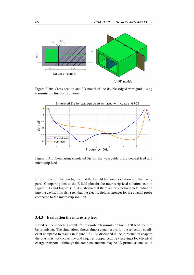
65 CHAPTER 3. DESIGN AND ANALYSIS
(a) Cross section.
(b) 3D model.
Figure 3.30: Cross section and 3D model of the double ridged waveguide using
transmission line feed solution.
2 3 4 5 6 7 8 9Frequency [GHz]
25
20
15
10
5
0
S 11 [
dB]
Simulated S11 for waveguide terminated with coax and PCB
Coaxial feedPCB feed
Figure 3.31: Comparing simulated S11 for the waveguide using coaxial feed and
microstrip feed.
It is observed in the two figures that the E-field has some radiation into the cavity
part. Comparing this to the E-field plot for the microstrip feed solution seen in
Figure 3.33 and Figure 3.35, it is shown that there are no electrical field radiation
into the cavity. It is also seen that the electric field is stronger for the coaxial probe
compared to the microstrip solution.
3.4.3 Evaluation the microstrip feed
Based on the modeling results for microstrip transmission line, PCB feed seem to
be promising. The simulations shows almost equal results for the reflection coeffi-
cient compared to results in Figure 3.31. As discussed in the introduction chapter,
the plastic is not conductive and requires copper coating (spraying) for electrical
charge transport. Although the complete antenna may be 3D printed as one, solid
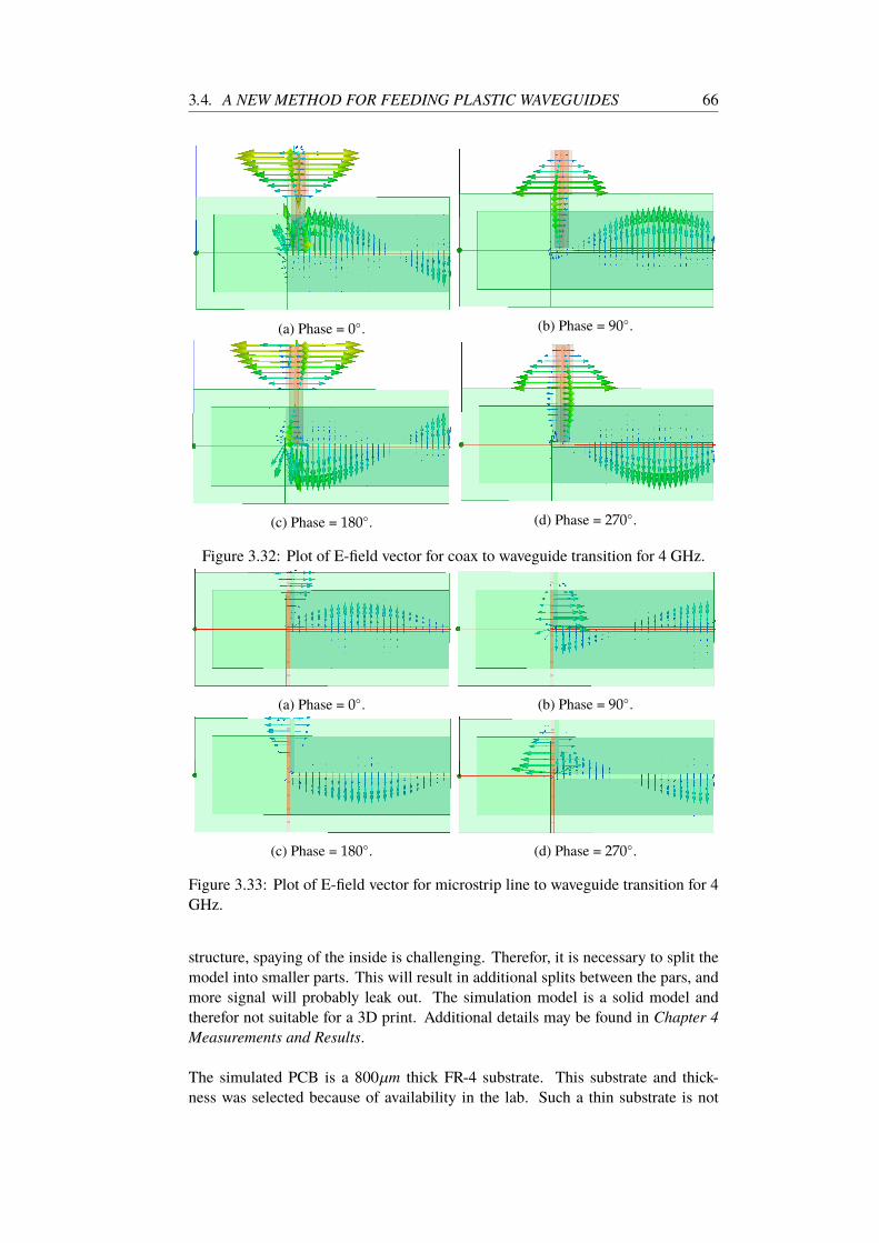
3.4. A NEW METHOD FOR FEEDING PLASTIC WAVEGUIDES 66
(a) Phase = 0. (b) Phase = 90.
(c) Phase = 180. (d) Phase = 270.
Figure 3.32: Plot of E-field vector for coax to waveguide transition for 4 GHz.
(a) Phase = 0. (b) Phase = 90.
(c) Phase = 180. (d) Phase = 270.
Figure 3.33: Plot of E-field vector for microstrip line to waveguide transition for 4
GHz.
structure, spaying of the inside is challenging. Therefor, it is necessary to split the
model into smaller parts. This will result in additional splits between the pars, and
more signal will probably leak out. The simulation model is a solid model and
therefor not suitable for a 3D print. Additional details may be found in Chapter 4
Measurements and Results.
The simulated PCB is a 800µm thick FR-4 substrate. This substrate and thick-
ness was selected because of availability in the lab. Such a thin substrate is not
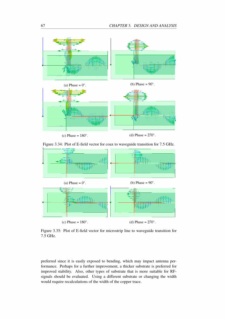
67 CHAPTER 3. DESIGN AND ANALYSIS
(a) Phase = 0. (b) Phase = 90.
(c) Phase = 180. (d) Phase = 270.
Figure 3.34: Plot of E-field vector for coax to waveguide transition for 7.5 GHz.
(a) Phase = 0. (b) Phase = 90.
(c) Phase = 180. (d) Phase = 270.
Figure 3.35: Plot of E-field vector for microstrip line to waveguide transition for
7.5 GHz.
preferred since it is easily exposed to bending, which may impact antenna per-
formance. Perhaps for a further improvement, a thicker substrate is preferred for
improved stability. Also, other types of substrate that is more suitable for RF-
signals should be evaluated. Using a different substrate or changing the width
would require recalculations of the width of the copper trace.
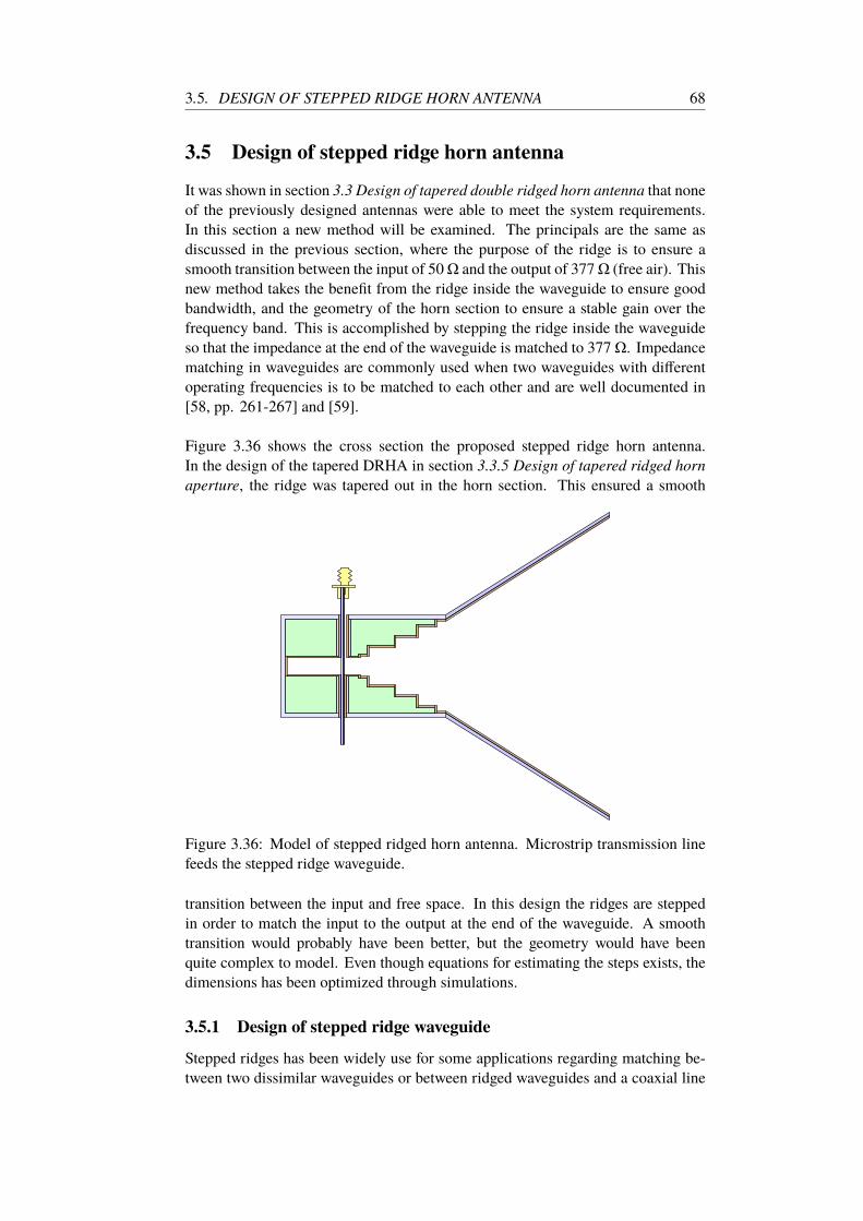
3.5. DESIGN OF STEPPED RIDGE HORN ANTENNA 68
3.5 Design of stepped ridge horn antenna
It was shown in section 3.3 Design of tapered double ridged horn antenna that none
of the previously designed antennas were able to meet the system requirements.
In this section a new method will be examined. The principals are the same as
discussed in the previous section, where the purpose of the ridge is to ensure a
smooth transition between the input of 50Ω and the output of 377Ω (free air). This
new method takes the benefit from the ridge inside the waveguide to ensure good
bandwidth, and the geometry of the horn section to ensure a stable gain over the
frequency band. This is accomplished by stepping the ridge inside the waveguide
so that the impedance at the end of the waveguide is matched to 377 Ω. Impedance
matching in waveguides are commonly used when two waveguides with different
operating frequencies is to be matched to each other and are well documented in
[58, pp. 261-267] and [59].
Figure 3.36 shows the cross section the proposed stepped ridge horn antenna.
In the design of the tapered DRHA in section 3.3.5 Design of tapered ridged horn
aperture, the ridge was tapered out in the horn section. This ensured a smooth
Figure 3.36: Model of stepped ridged horn antenna. Microstrip transmission line
feeds the stepped ridge waveguide.
transition between the input and free space. In this design the ridges are stepped
in order to match the input to the output at the end of the waveguide. A smooth
transition would probably have been better, but the geometry would have been
quite complex to model. Even though equations for estimating the steps exists, the
dimensions has been optimized through simulations.
3.5.1 Design of stepped ridge waveguide
Stepped ridges has been widely use for some applications regarding matching be-
tween two dissimilar waveguides or between ridged waveguides and a coaxial line
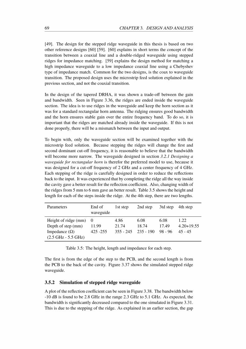
69 CHAPTER 3. DESIGN AND ANALYSIS
[49]. The design for the stepped ridge waveguide in this thesis is based on two
other reference designs [60] [59]. [60] explains in short terms the concept of the
transition between a coaxial line and a double-ridged waveguide using stepped
ridges for impedance matching. [59] explains the design method for matching a
high impedance waveguide to a low impedance coaxial line using a Chebyshev
type of impedance match. Common for the two designs, is the coax to waveguide
transition. The proposed design uses the microstrip feed solution explained in the
previous section, and not the coaxial transition.
In the design of the tapered DRHA, it was shown a trade-off between the gain
and bandwidth. Seen in Figure 3.36, the ridges are ended inside the waveguide
section. The idea is to use ridges in the waveguide and keep the horn section as it
was for a standard rectangular horn antenna. The ridging ensures good bandwidth
and the horn ensures stable gain over the entire frequency band. To do so, it is
important that the ridges are matched already inside the waveguide. If this is not
done properly, there will be a mismatch between the input and output.
To begin with, only the waveguide section will be examined together with the
microstrip feed solution. Because stepping the ridges will change the first and
second dominant cut-off frequency, it is reasonable to believe that the bandwidth
will become more narrow. The waveguide designed in section 3.2.1 Designing a
waveguide for rectangular horn is therefor the preferred model to use, because it
was designed for a cut-off frequency of 2 GHz and a center frequency of 4 GHz.
Each stepping of the ridge is carefully designed in order to reduce the reflections
back to the input. It was experienced that by completing the ridge all the way inside
the cavity gave a better result for the reflection coefficient. Also, changing width of
the ridges from 5 mm to 6 mm gave an better result. Table 3.5 shows the height and
length for each of the steps inside the ridge. At the 4th step, there are two lengths.
Parameters End of 1st step 2nd step 3td step 4th step
waveguide
Height of ridge (mm) 0 4.86 6.08 6.08 1.22
Depth of step (mm) 11.99 21.74 18.74 17.49 4.20+19.55
Impedance (Ω) 425 -255 355 - 245 235 - 190 98 - 96 45 - 45
(2.5 GHz - 5.5 GHz)
Table 3.5: The height, length and impedance for each step.
The first is from the edge of the step to the PCB, and the second length is from
the PCB to the back of the cavity. Figure 3.37 shows the simulated stepped ridge
waveguide.
3.5.2 Simulation of stepped ridge waveguide
A plot of the reflection coefficient can be seen in Figure 3.38. The bandwidth below
-10 dB is found to be 2.8 GHz in the range 2.3 GHz to 5.1 GHz. As expected, the
bandwidth is significantly decreased compared to the one simulated in Figure 3.31.
This is due to the stepping of the ridge. As explained in an earlier section, the gap
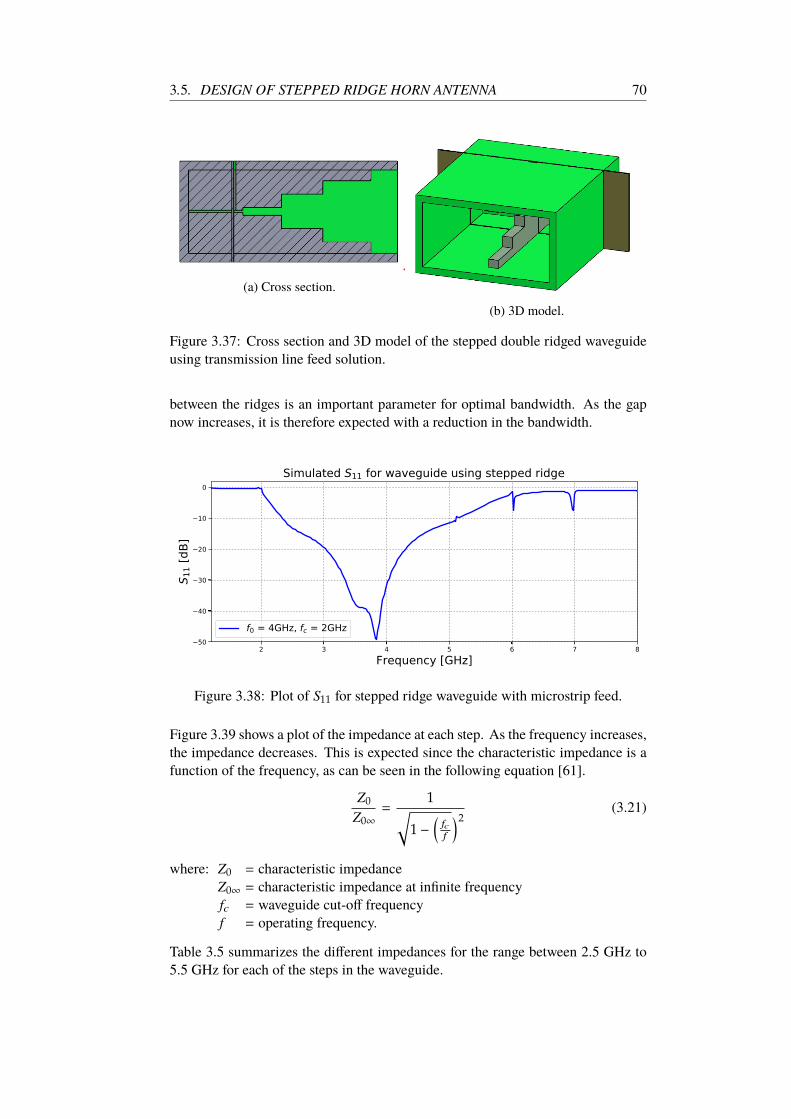
3.5. DESIGN OF STEPPED RIDGE HORN ANTENNA 70
(a) Cross section.
(b) 3D model.
Figure 3.37: Cross section and 3D model of the stepped double ridged waveguide
using transmission line feed solution.
between the ridges is an important parameter for optimal bandwidth. As the gap
now increases, it is therefore expected with a reduction in the bandwidth.
2 3 4 5 6 7 8Frequency [GHz]
50
40
30
20
10
0
S 11 [
dB]
Simulated S11 for waveguide using stepped ridge
f0 = 4GHz, fc = 2GHz
Figure 3.38: Plot of S11 for stepped ridge waveguide with microstrip feed.
Figure 3.39 shows a plot of the impedance at each step. As the frequency increases,
the impedance decreases. This is expected since the characteristic impedance is a
function of the frequency, as can be seen in the following equation [61].
Z0
Z0∞=
1√
1 −(
fcf
)2(3.21)
where: Z0 = characteristic impedance
Z0∞ = characteristic impedance at infinite frequency
fc = waveguide cut-off frequency
f = operating frequency.
Table 3.5 summarizes the different impedances for the range between 2.5 GHz to
5.5 GHz for each of the steps in the waveguide.
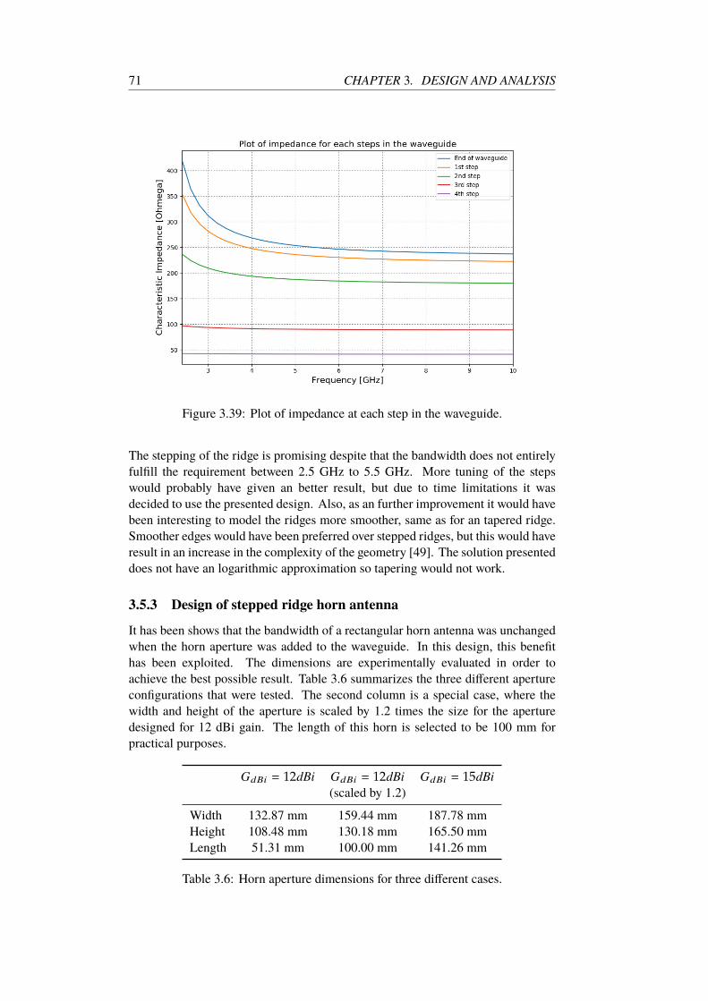
71 CHAPTER 3. DESIGN AND ANALYSIS
Figure 3.39: Plot of impedance at each step in the waveguide.
The stepping of the ridge is promising despite that the bandwidth does not entirely
fulfill the requirement between 2.5 GHz to 5.5 GHz. More tuning of the steps
would probably have given an better result, but due to time limitations it was
decided to use the presented design. Also, as an further improvement it would have
been interesting to model the ridges more smoother, same as for an tapered ridge.
Smoother edges would have been preferred over stepped ridges, but this would have
result in an increase in the complexity of the geometry [49]. The solution presented
does not have an logarithmic approximation so tapering would not work.
3.5.3 Design of stepped ridge horn antenna
It has been shows that the bandwidth of a rectangular horn antenna was unchanged
when the horn aperture was added to the waveguide. In this design, this benefit
has been exploited. The dimensions are experimentally evaluated in order to
achieve the best possible result. Table 3.6 summarizes the three different aperture
configurations that were tested. The second column is a special case, where the
width and height of the aperture is scaled by 1.2 times the size for the aperture
designed for 12 dBi gain. The length of this horn is selected to be 100 mm for
practical purposes.
GdBi = 12dBi GdBi = 12dBi GdBi = 15dBi
(scaled by 1.2)
Width 132.87 mm 159.44 mm 187.78 mm
Height 108.48 mm 130.18 mm 165.50 mm
Length 51.31 mm 100.00 mm 141.26 mm
Table 3.6: Horn aperture dimensions for three different cases.
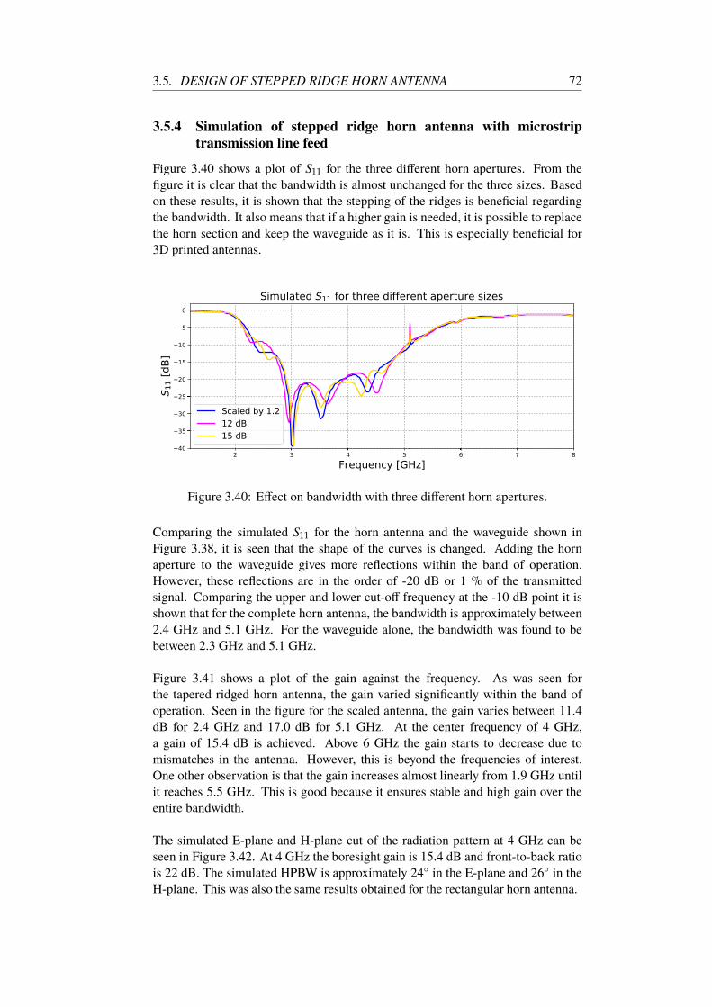
3.5. DESIGN OF STEPPED RIDGE HORN ANTENNA 72
3.5.4 Simulation of stepped ridge horn antenna with microstrip
transmission line feed
Figure 3.40 shows a plot of S11 for the three different horn apertures. From the
figure it is clear that the bandwidth is almost unchanged for the three sizes. Based
on these results, it is shown that the stepping of the ridges is beneficial regarding
the bandwidth. It also means that if a higher gain is needed, it is possible to replace
the horn section and keep the waveguide as it is. This is especially beneficial for
3D printed antennas.
2 3 4 5 6 7 8Frequency [GHz]
40
35
30
25
20
15
10
5
0
S 11 [
dB]
Simulated S11 for three different aperture sizes
Scaled by 1.212 dBi15 dBi
Figure 3.40: Effect on bandwidth with three different horn apertures.
Comparing the simulated S11 for the horn antenna and the waveguide shown in
Figure 3.38, it is seen that the shape of the curves is changed. Adding the horn
aperture to the waveguide gives more reflections within the band of operation.
However, these reflections are in the order of -20 dB or 1 % of the transmitted
signal. Comparing the upper and lower cut-off frequency at the -10 dB point it is
shown that for the complete horn antenna, the bandwidth is approximately between
2.4 GHz and 5.1 GHz. For the waveguide alone, the bandwidth was found to be
between 2.3 GHz and 5.1 GHz.
Figure 3.41 shows a plot of the gain against the frequency. As was seen for
the tapered ridged horn antenna, the gain varied significantly within the band of
operation. Seen in the figure for the scaled antenna, the gain varies between 11.4
dB for 2.4 GHz and 17.0 dB for 5.1 GHz. At the center frequency of 4 GHz,
a gain of 15.4 dB is achieved. Above 6 GHz the gain starts to decrease due to
mismatches in the antenna. However, this is beyond the frequencies of interest.
One other observation is that the gain increases almost linearly from 1.9 GHz until
it reaches 5.5 GHz. This is good because it ensures stable and high gain over the
entire bandwidth.
The simulated E-plane and H-plane cut of the radiation pattern at 4 GHz can be
seen in Figure 3.42. At 4 GHz the boresight gain is 15.4 dB and front-to-back ratio
is 22 dB. The simulated HPBW is approximately 24 in the E-plane and 26 in the
H-plane. This was also the same results obtained for the rectangular horn antenna.

73 CHAPTER 3. DESIGN AND ANALYSIS
2 3 4 5 6 7 8Frequency [GHz]
0.0
2.5
5.0
7.5
10.0
12.5
15.0
17.5
20.0Ga
in [d
B]Simulated gain versus the frequency for three different aperture sizes
Scaled by 1.212 dBi15 dBi
Figure 3.41: Plot of gain versus frequency for three different aperture sizes.
150 100 50 0 50 100 150Frequency [GHz]
30
20
10
0
10
Gain
[dB]
Simulated E-plane and H-plane for stepped ridged horn antennaE-planeH-plane
Figure 3.42: Plot of E- and H-plane directivity at 4 GHz for the stepped ridge horn
antenna with mictrostrip transmission line feed. Peak gain of 15.4 dBi. HPBW of
24 in E-plane and 26 in H-field.
3.5.5 Summary of stepped ridge horn antenna
The stepped ridge horn antenna (SRHA) with the new feed solution looks promis-
ing despite that the requirement for the bandwidth was not entirely fulfilled. As
explained in Chapter 2, the Ventricorder radar module has the ability to switch be-
tween different PG-selections. If the center frequency is set to an lower frequency,
the antennas with the achieved bandwidth will work fine. The problem arises when
the center frequency are shifted to an higher frequency. The achieved bandwidth
of 2.7 GHz in the range 2.4 GHz to 5.1 GHz will therefore work fine for lower
PF-selections.
The new feed solution matches the traditional coaxial probe feed. This is very
beneficial regarding the implementation to the 3D printed horn antenna. In addi-
tion, for a system without RF cables where the radar and antenna feed is assembled
on the same PCB is feasible removing the cost of SMA connectors and RF cables.
3.6. 3D PRINTED ANTENNAS 74
3.6 3D printed antennas
The focus in this thesis is to create a 3D printed horn antenna using low cost
thermoplastic polymers (ABS, PLA). So fare the discussion has been focused
on the design of the horn antenna discussing the performance of different types
of configurations. To meet the requirements for the remote Geo-Sensing, it is
important that the system is light weighted and easy to carry. Fabricated horn
antennas that matches the size of the one designed in the previous section, weights
about 1.6 Kg [62]. For a complete radar system, two of these antennas are needed,
resulting in a total weight of 3.2 Kg, only for the antennas. Also, the price is an
crucial factor. Antennas in the same category, costs about $3,500.00. Both reducing
the weight and cost are two important aspects regarding 3D printed antennas. Some
work has been developed regarding metalized 3D printed plastic antennas, and the
performance matches the machined [30] [31].
3.6.1 Challenges by 3D printing antennas
As was explained in Section 3.4 A new method for feeding plastic waveguides prob-
lems arises regarding the feeding of the plastic waveguide. As a proposal to this
problem, a PCB feed is placed between the cavity and the waveguide. Splitting
the waveguide is not preferred as the RF-signals may leak out in the gaps between
the 3D printed parts. Minimizing this risk is therefore extremely important for
maximum performance.
Another problem that arises, is the metallization of the plastic parts. PLA has
a permittivity of approximately 3.5 [63] which means that if the 3D part is not en-
tirely copper coated, the RF signal will leak out from the uncovered areas. In order
to ensure good copper coating, the model has to be split into several smaller parts.
Regarding the metallization, the copper coating spray will contribute to much more
electrical losses compared to a conventional metal antenna. The resistive losses for
three copper coated layers is 0.011 Ω/sq [64]. This assumes that the entire model
is equally coated. The resistive losses have been simulated in HFSS on the same
antenna model explained in the previous section, to see the difference between PEC
and realistic values for the electrical conductor. The results can be seen in Figure
3.43.
Simulations shows minor differences in the PEC simulated model and the one with
realistic values. However, this assumes that the copper is equally coated over the
entire surface. In addition, the model has been simulated as a solid model covered
with the realistic material, and not specified for any layer thickness.
3.6.2 3D printed stepped ridge horn antenna
To minimize the risk of leakage of the RF-signal, it is crucial that the mechanical
parts of the antenna is designed properly. Figure 3.44 shows a model of the printed
SRHA designed in HFSS (see Appendix B for machine drawings). The horn aper-
ture is split into four parts, one for each of the walls. To assemble the walls, the
parts are screwed together at the outside of the antenna, as can be seen in the
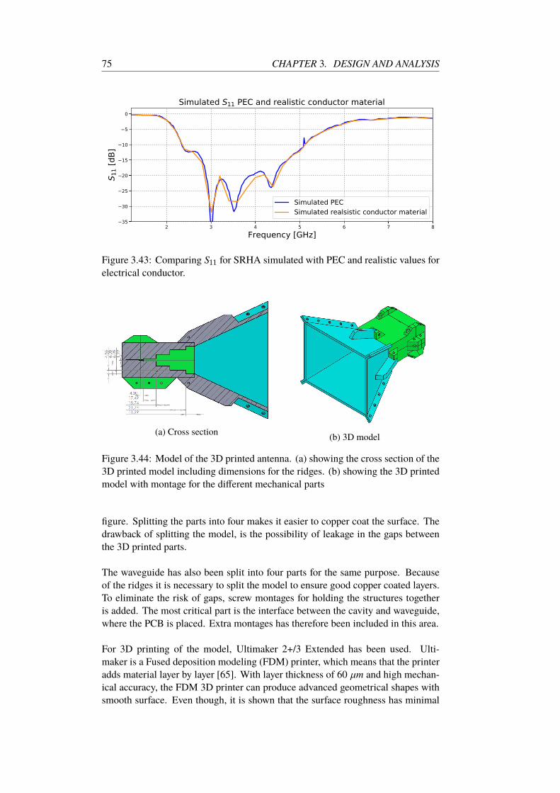
75 CHAPTER 3. DESIGN AND ANALYSIS
2 3 4 5 6 7 8Frequency [GHz]
35
30
25
20
15
10
5
0S 1
1 [dB
]Simulated S11 PEC and realistic conductor material
Simulated PECSimulated realsistic conductor material
Figure 3.43: Comparing S11 for SRHA simulated with PEC and realistic values for
electrical conductor.
(a) Cross section(b) 3D model
Figure 3.44: Model of the 3D printed antenna. (a) showing the cross section of the
3D printed model including dimensions for the ridges. (b) showing the 3D printed
model with montage for the different mechanical parts
figure. Splitting the parts into four makes it easier to copper coat the surface. The
drawback of splitting the model, is the possibility of leakage in the gaps between
the 3D printed parts.
The waveguide has also been split into four parts for the same purpose. Because
of the ridges it is necessary to split the model to ensure good copper coated layers.
To eliminate the risk of gaps, screw montages for holding the structures together
is added. The most critical part is the interface between the cavity and waveguide,
where the PCB is placed. Extra montages has therefore been included in this area.
For 3D printing of the model, Ultimaker 2+/3 Extended has been used. Ulti-
maker is a Fused deposition modeling (FDM) printer, which means that the printer
adds material layer by layer [65]. With layer thickness of 60 µm and high mechan-
ical accuracy, the FDM 3D printer can produce advanced geometrical shapes with
smooth surface. Even though, it is shown that the surface roughness has minimal
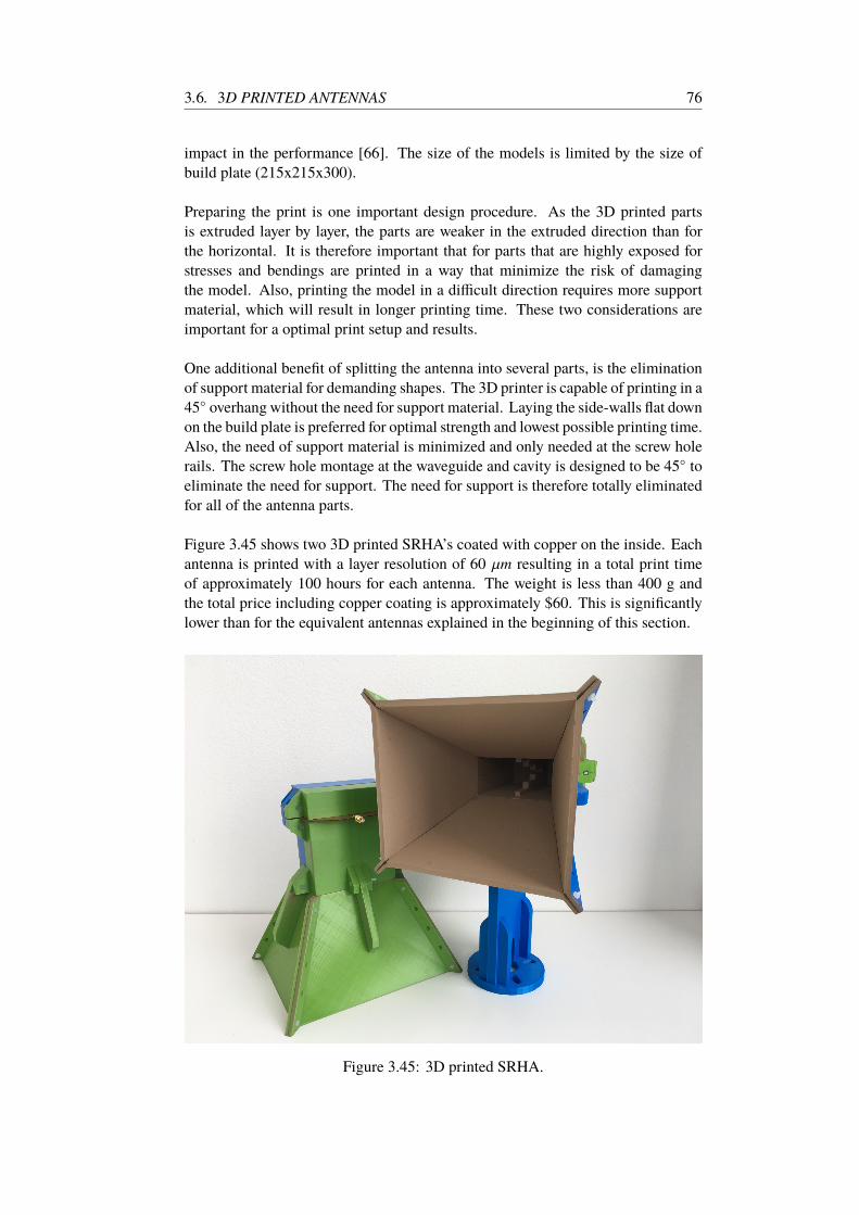
3.6. 3D PRINTED ANTENNAS 76
impact in the performance [66]. The size of the models is limited by the size of
build plate (215x215x300).
Preparing the print is one important design procedure. As the 3D printed parts
is extruded layer by layer, the parts are weaker in the extruded direction than for
the horizontal. It is therefore important that for parts that are highly exposed for
stresses and bendings are printed in a way that minimize the risk of damaging
the model. Also, printing the model in a difficult direction requires more support
material, which will result in longer printing time. These two considerations are
important for a optimal print setup and results.
One additional benefit of splitting the antenna into several parts, is the elimination
of support material for demanding shapes. The 3D printer is capable of printing in a
45 overhang without the need for support material. Laying the side-walls flat down
on the build plate is preferred for optimal strength and lowest possible printing time.
Also, the need of support material is minimized and only needed at the screw hole
rails. The screw hole montage at the waveguide and cavity is designed to be 45 to
eliminate the need for support. The need for support is therefore totally eliminated
for all of the antenna parts.
Figure 3.45 shows two 3D printed SRHA’s coated with copper on the inside. Each
antenna is printed with a layer resolution of 60 µm resulting in a total print time
of approximately 100 hours for each antenna. The weight is less than 400 g and
the total price including copper coating is approximately $60. This is significantly
lower than for the equivalent antennas explained in the beginning of this section.
Figure 3.45: 3D printed SRHA.
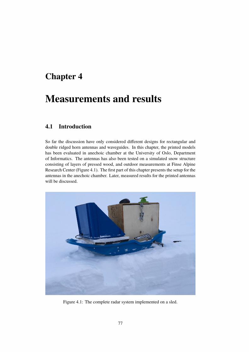
Chapter 4
Measurements and results
4.1 Introduction
So far the discussion have only considered different designs for rectangular and
double ridged horn antennas and waveguides. In this chapter, the printed models
has been evaluated in anechoic chamber at the University of Oslo, Department
of Informatics. The antennas has also been tested on a simulated snow structure
consisting of layers of pressed wood, and outdoor measurements at Finse Alpine
Research Center (Figure 4.1). The first part of this chapter presents the setup for the
antennas in the anechoic chamber. Later, measured results for the printed antennas
will be discussed.
Figure 4.1: The complete radar system implemented on a sled.
77
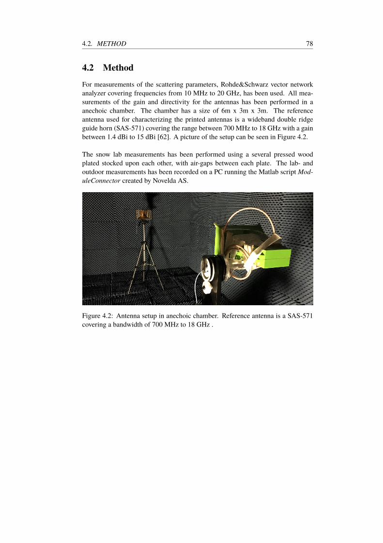
4.2. METHOD 78
4.2 Method
For measurements of the scattering parameters, Rohde&Schwarz vector network
analyzer covering frequencies from 10 MHz to 20 GHz, has been used. All mea-
surements of the gain and directivity for the antennas has been performed in a
anechoic chamber. The chamber has a size of 6m x 3m x 3m. The reference
antenna used for characterizing the printed antennas is a wideband double ridge
guide horn (SAS-571) covering the range between 700 MHz to 18 GHz with a gain
between 1.4 dBi to 15 dBi [62]. A picture of the setup can be seen in Figure 4.2.
The snow lab measurements has been performed using a several pressed wood
plated stocked upon each other, with air-gaps between each plate. The lab- and
outdoor measurements has been recorded on a PC running the Matlab script Mod-
uleConnector created by Novelda AS.
Figure 4.2: Antenna setup in anechoic chamber. Reference antenna is a SAS-571
covering a bandwidth of 700 MHz to 18 GHz .
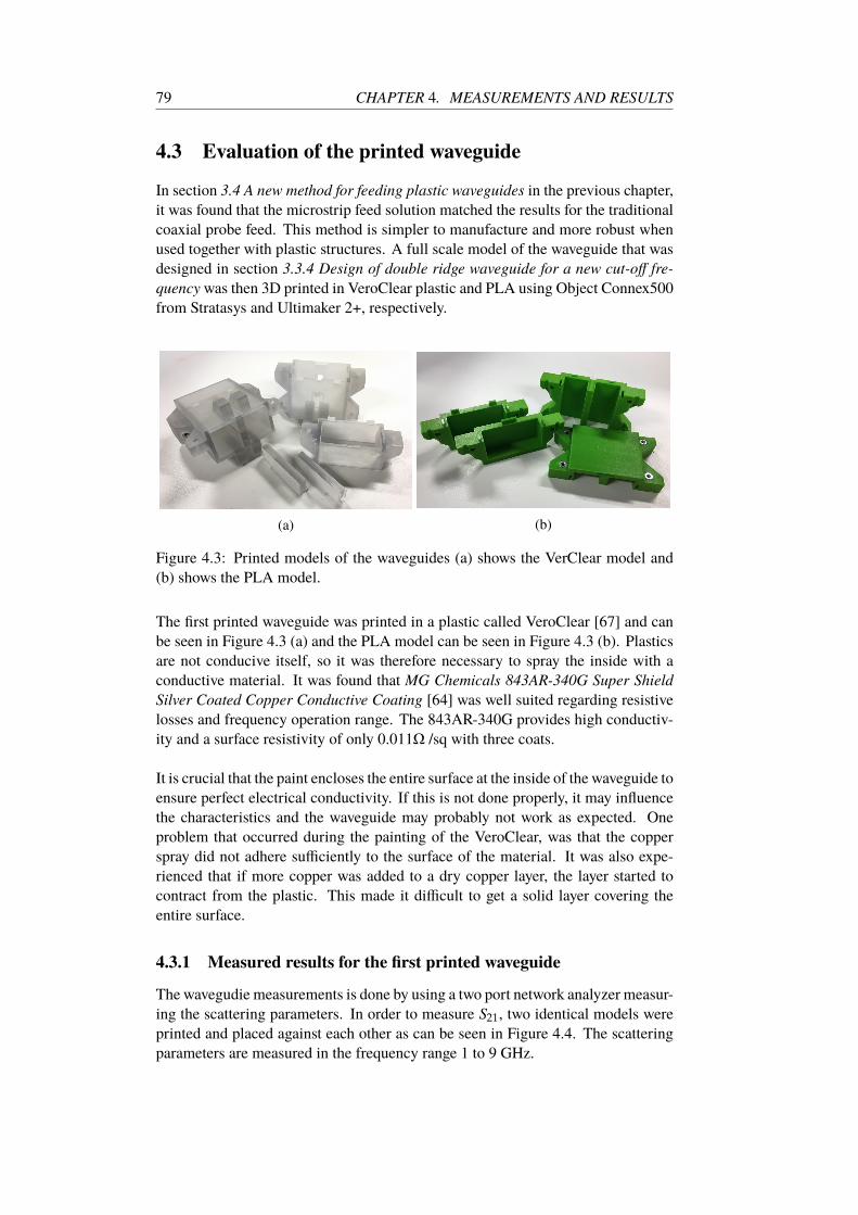
79 CHAPTER 4. MEASUREMENTS AND RESULTS
4.3 Evaluation of the printed waveguide
In section 3.4 A new method for feeding plastic waveguides in the previous chapter,
it was found that the microstrip feed solution matched the results for the traditional
coaxial probe feed. This method is simpler to manufacture and more robust when
used together with plastic structures. A full scale model of the waveguide that was
designed in section 3.3.4 Design of double ridge waveguide for a new cut-off fre-
quency was then 3D printed in VeroClear plastic and PLA using Object Connex500
from Stratasys and Ultimaker 2+, respectively.
(a) (b)
Figure 4.3: Printed models of the waveguides (a) shows the VerClear model and
(b) shows the PLA model.
The first printed waveguide was printed in a plastic called VeroClear [67] and can
be seen in Figure 4.3 (a) and the PLA model can be seen in Figure 4.3 (b). Plastics
are not conducive itself, so it was therefore necessary to spray the inside with a
conductive material. It was found that MG Chemicals 843AR-340G Super Shield
Silver Coated Copper Conductive Coating [64] was well suited regarding resistive
losses and frequency operation range. The 843AR-340G provides high conductiv-
ity and a surface resistivity of only 0.011Ω /sq with three coats.
It is crucial that the paint encloses the entire surface at the inside of the waveguide to
ensure perfect electrical conductivity. If this is not done properly, it may influence
the characteristics and the waveguide may probably not work as expected. One
problem that occurred during the painting of the VeroClear, was that the copper
spray did not adhere sufficiently to the surface of the material. It was also expe-
rienced that if more copper was added to a dry copper layer, the layer started to
contract from the plastic. This made it difficult to get a solid layer covering the
entire surface.
4.3.1 Measured results for the first printed waveguide
The wavegudie measurements is done by using a two port network analyzer measur-
ing the scattering parameters. In order to measure S21, two identical models were
printed and placed against each other as can be seen in Figure 4.4. The scattering
parameters are measured in the frequency range 1 to 9 GHz.
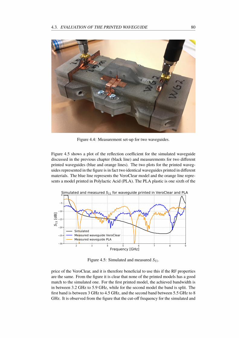
4.3. EVALUATION OF THE PRINTED WAVEGUIDE 80
Figure 4.4: Measurement set-up for two waveguides.
Figure 4.5 shows a plot of the reflection coefficient for the simulated waveguide
discussed in the previous chapter (black line) and measurements for two different
printed waveguides (blue and orange lines). The two plots for the printed waveg-
uides represented in the figure is in fact two identical waveguides printed in different
materials. The blue line represents the VeroClear model and the orange line repre-
sents a model printed in Polylactic Acid (PLA). The PLA plastic is one sixth of the
2 3 4 5 6 7 8 9Frequency [GHz]
30
25
20
15
10
5
0
S 11 [
dB]
Simulated and measured S11 for waveguide printed in VeroClear and PLA
SimulatedMeasured waveguide VeroClearMeasured waveguide PLA
Figure 4.5: Simulated and measured S11.
price of the VeroClear, and it is therefore beneficial to use this if the RF properties
are the same. From the figure it is clear that none of the printed models has a good
match to the simulated one. For the first printed model, the achieved bandwidth is
in between 3.2 GHz to 5.9 GHz, while for the second model the band is split. The
first band is between 3 GHz to 4.5 GHz, and the second band between 5.5 GHz to 8
GHz. It is observed from the figure that the cut-off frequency for the simulated and
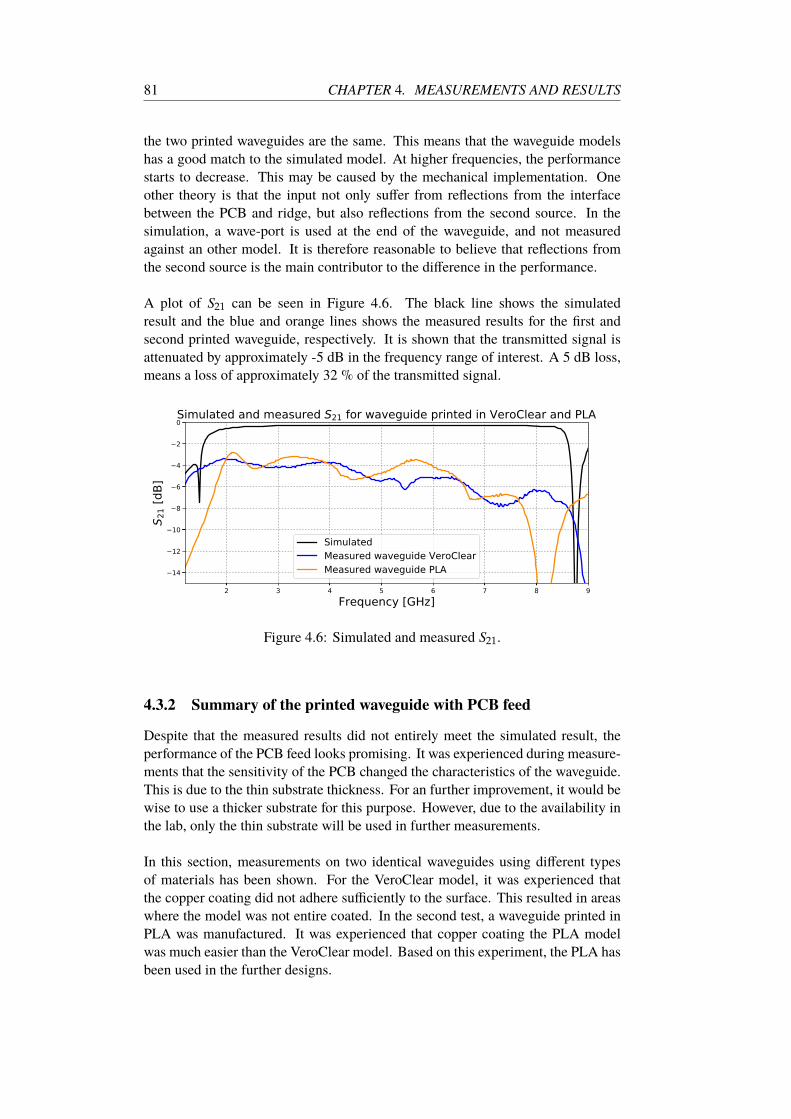
81 CHAPTER 4. MEASUREMENTS AND RESULTS
the two printed waveguides are the same. This means that the waveguide models
has a good match to the simulated model. At higher frequencies, the performance
starts to decrease. This may be caused by the mechanical implementation. One
other theory is that the input not only suffer from reflections from the interface
between the PCB and ridge, but also reflections from the second source. In the
simulation, a wave-port is used at the end of the waveguide, and not measured
against an other model. It is therefore reasonable to believe that reflections from
the second source is the main contributor to the difference in the performance.
A plot of S21 can be seen in Figure 4.6. The black line shows the simulated
result and the blue and orange lines shows the measured results for the first and
second printed waveguide, respectively. It is shown that the transmitted signal is
attenuated by approximately -5 dB in the frequency range of interest. A 5 dB loss,
means a loss of approximately 32 % of the transmitted signal.
2 3 4 5 6 7 8 9Frequency [GHz]
14
12
10
8
6
4
2
0
S 21 [
dB]
Simulated and measured S21 for waveguide printed in VeroClear and PLA
SimulatedMeasured waveguide VeroClearMeasured waveguide PLA
Figure 4.6: Simulated and measured S21.
4.3.2 Summary of the printed waveguide with PCB feed
Despite that the measured results did not entirely meet the simulated result, the
performance of the PCB feed looks promising. It was experienced during measure-
ments that the sensitivity of the PCB changed the characteristics of the waveguide.
This is due to the thin substrate thickness. For an further improvement, it would be
wise to use a thicker substrate for this purpose. However, due to the availability in
the lab, only the thin substrate will be used in further measurements.
In this section, measurements on two identical waveguides using different types
of materials has been shown. For the VeroClear model, it was experienced that
the copper coating did not adhere sufficiently to the surface. This resulted in areas
where the model was not entire coated. In the second test, a waveguide printed in
PLA was manufactured. It was experienced that copper coating the PLA model
was much easier than the VeroClear model. Based on this experiment, the PLA has
been used in the further designs.

4.3. EVALUATION OF THE PRINTED WAVEGUIDE 82
The measurements on the waveguide was carried out in order to test the perfor-
mance of the PCB feed. The models were designed in an early stage of the thesis,
and turned out to not be suited for the complete antenna system. This has been
explained in detail in the previous chapter. In the next section, the performance of
the antenna designed in section 3.5.3 Design of stepped ridge horn antenna will be
examined.
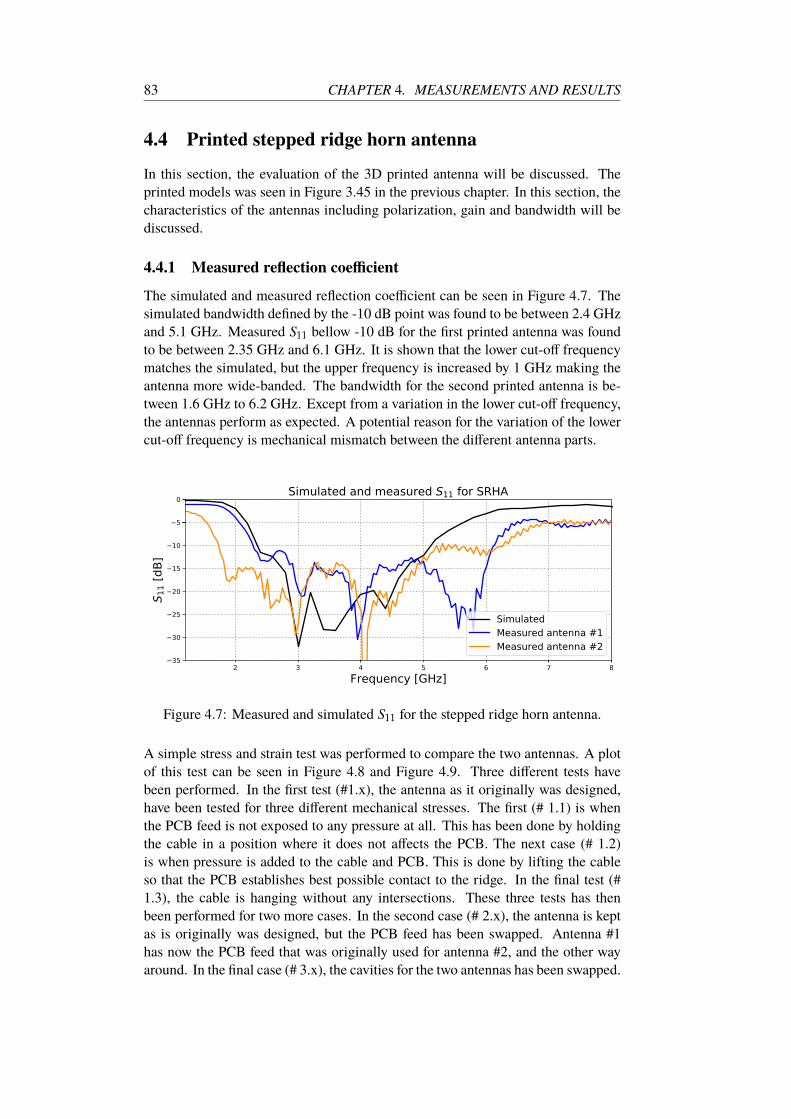
83 CHAPTER 4. MEASUREMENTS AND RESULTS
4.4 Printed stepped ridge horn antenna
In this section, the evaluation of the 3D printed antenna will be discussed. The
printed models was seen in Figure 3.45 in the previous chapter. In this section, the
characteristics of the antennas including polarization, gain and bandwidth will be
discussed.
4.4.1 Measured reflection coefficient
The simulated and measured reflection coefficient can be seen in Figure 4.7. The
simulated bandwidth defined by the -10 dB point was found to be between 2.4 GHz
and 5.1 GHz. Measured S11 bellow -10 dB for the first printed antenna was found
to be between 2.35 GHz and 6.1 GHz. It is shown that the lower cut-off frequency
matches the simulated, but the upper frequency is increased by 1 GHz making the
antenna more wide-banded. The bandwidth for the second printed antenna is be-
tween 1.6 GHz to 6.2 GHz. Except from a variation in the lower cut-off frequency,
the antennas perform as expected. A potential reason for the variation of the lower
cut-off frequency is mechanical mismatch between the different antenna parts.
2 3 4 5 6 7 8Frequency [GHz]
35
30
25
20
15
10
5
0
S 11 [
dB]
Simulated and measured S11 for SRHA
SimulatedMeasured antenna #1Measured antenna #2
Figure 4.7: Measured and simulated S11 for the stepped ridge horn antenna.
A simple stress and strain test was performed to compare the two antennas. A plot
of this test can be seen in Figure 4.8 and Figure 4.9. Three different tests have
been performed. In the first test (#1.x), the antenna as it originally was designed,
have been tested for three different mechanical stresses. The first (# 1.1) is when
the PCB feed is not exposed to any pressure at all. This has been done by holding
the cable in a position where it does not affects the PCB. The next case (# 1.2)
is when pressure is added to the cable and PCB. This is done by lifting the cable
so that the PCB establishes best possible contact to the ridge. In the final test (#
1.3), the cable is hanging without any intersections. These three tests has then
been performed for two more cases. In the second case (# 2.x), the antenna is kept
as is originally was designed, but the PCB feed has been swapped. Antenna #1
has now the PCB feed that was originally used for antenna #2, and the other way
around. In the final case (# 3.x), the cavities for the two antennas has been swapped.
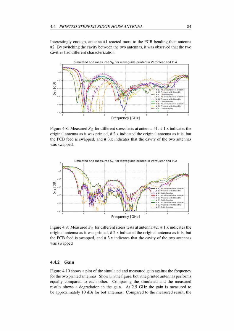
4.4. PRINTED STEPPED RIDGE HORN ANTENNA 84
Interestingly enough, antenna #1 reacted more to the PCB bending than antenna
#2. By switching the cavity between the two antennas, it was observed that the two
cavities had different characterization.
1 2 3 4 5 6 7Frequency [GHz]
30
25
20
15
10
5
0
S 11 [
dB]
Simulated and measured S11 for waveguide printed in VeroClear and PLA
# 1.1 No pressure added to cable# 1.2 Pressure added to cable# 1.3 Cable hanging# 2.1 No pressure added to cable# 2.2 Pressure added to cable# 2.3 Cable hanging# 3.1 No pressure added to cable# 3.2 Pressure added to cable# 3.3 Cable hanging
Figure 4.8: Measured S11 for different stress tests at antenna #1. # 1.x indicates the
original antenna as it was printed, # 2.x indicated the original antenna as it is, but
the PCB feed is swapped, and # 3.x indicates that the cavity of the two antennas
was swapped.
1 2 3 4 5 6 7Frequency [GHz]
30
25
20
15
10
5
0
S 11 [
dB]
Simulated and measured S11 for waveguide printed in VeroClear and PLA
# 1.1 No pressure added to cable# 1.2 Pressure added to cable# 1.3 Cable hanging# 2.1 No pressure added to cable# 2.2 Pressure added to cable# 2.3 Cable hanging# 3.1 No pressure added to cable# 3.2 Pressure added to cable# 3.3 Cable hanging
Figure 4.9: Measured S11 for different stress tests at antenna #2. # 1.x indicates the
original antenna as it was printed, # 2.x indicated the original antenna as it is, but
the PCB feed is swapped, and # 3.x indicates that the cavity of the two antennas
was swapped
4.4.2 Gain
Figure 4.10 shows a plot of the simulated and measured gain against the frequency
for the two printed antennas. Shown in the figure, both the printed antennas performs
equally compared to each other. Comparing the simulated and the measured
results shows a degradation in the gain. At 2.5 GHz the gain is measured to
be approximately 10 dBi for bot antennas. Compared to the measured result, the
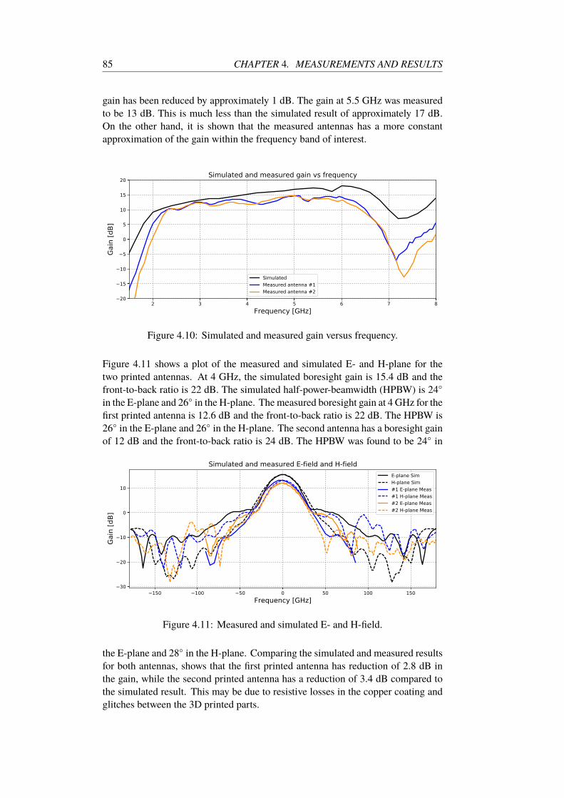
85 CHAPTER 4. MEASUREMENTS AND RESULTS
gain has been reduced by approximately 1 dB. The gain at 5.5 GHz was measured
to be 13 dB. This is much less than the simulated result of approximately 17 dB.
On the other hand, it is shown that the measured antennas has a more constant
approximation of the gain within the frequency band of interest.
2 3 4 5 6 7 8Frequency [GHz]
20
15
10
5
0
5
10
15
20
Gain
[dB]
Simulated and measured gain vs frequency
SimulatedMeasured antenna #1Measured antenna #2
Figure 4.10: Simulated and measured gain versus frequency.
Figure 4.11 shows a plot of the measured and simulated E- and H-plane for the
two printed antennas. At 4 GHz, the simulated boresight gain is 15.4 dB and the
front-to-back ratio is 22 dB. The simulated half-power-beamwidth (HPBW) is 24
in the E-plane and 26 in the H-plane. The measured boresight gain at 4 GHz for the
first printed antenna is 12.6 dB and the front-to-back ratio is 22 dB. The HPBW is
26 in the E-plane and 26 in the H-plane. The second antenna has a boresight gain
of 12 dB and the front-to-back ratio is 24 dB. The HPBW was found to be 24 in
150 100 50 0 50 100 150Frequency [GHz]
30
20
10
0
10
Gain
[dB]
Simulated and measured E-field and H-fieldE-plane SimH-plane Sim#1 E-plane Meas#1 H-plane Meas#2 E-plane Meas#2 H-plane Meas
Figure 4.11: Measured and simulated E- and H-field.
the E-plane and 28 in the H-plane. Comparing the simulated and measured results
for both antennas, shows that the first printed antenna has reduction of 2.8 dB in
the gain, while the second printed antenna has a reduction of 3.4 dB compared to
the simulated result. This may be due to resistive losses in the copper coating and
glitches between the 3D printed parts.
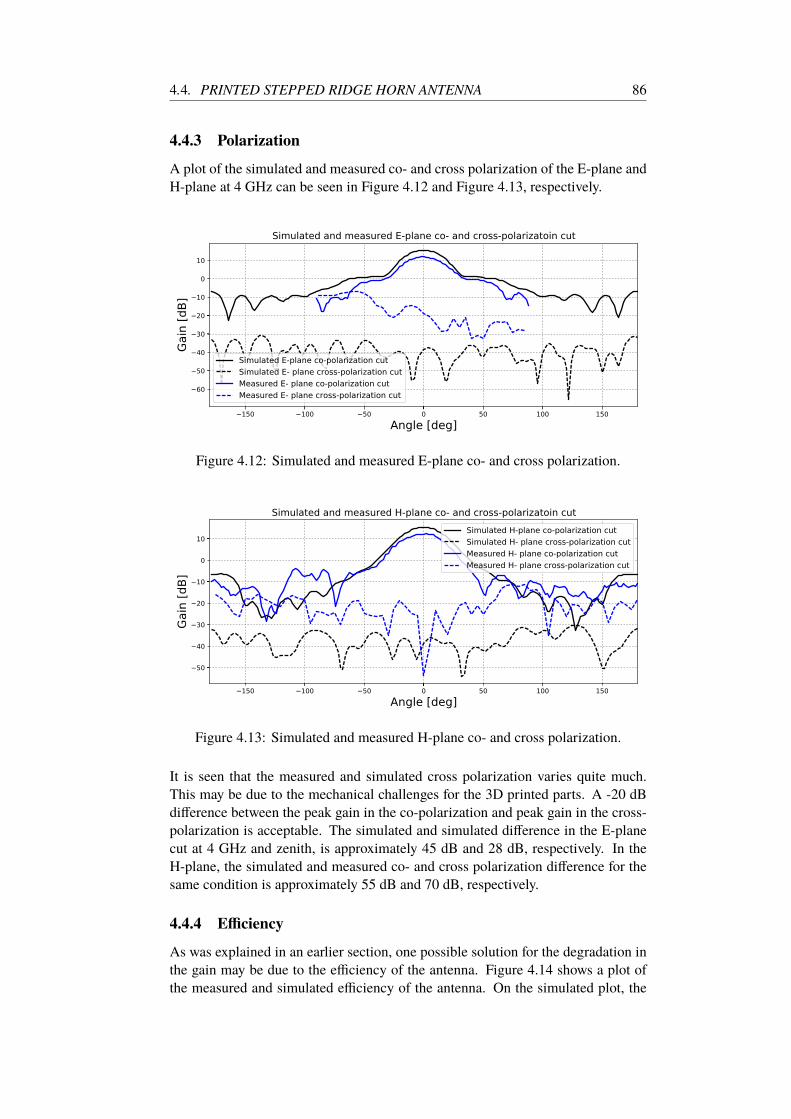
4.4. PRINTED STEPPED RIDGE HORN ANTENNA 86
4.4.3 Polarization
A plot of the simulated and measured co- and cross polarization of the E-plane and
H-plane at 4 GHz can be seen in Figure 4.12 and Figure 4.13, respectively.
150 100 50 0 50 100 150Angle [deg]
60
50
40
30
20
10
0
10
Gain
[dB]
Simulated and measured E-plane co- and cross-polarizatoin cut
Simulated E-plane co-polarization cutSimulated E- plane cross-polarization cutMeasured E- plane co-polarization cutMeasured E- plane cross-polarization cut
Figure 4.12: Simulated and measured E-plane co- and cross polarization.
150 100 50 0 50 100 150Angle [deg]
50
40
30
20
10
0
10
Gain
[dB]
Simulated and measured H-plane co- and cross-polarizatoin cutSimulated H-plane co-polarization cutSimulated H- plane cross-polarization cutMeasured H- plane co-polarization cutMeasured H- plane cross-polarization cut
Figure 4.13: Simulated and measured H-plane co- and cross polarization.
It is seen that the measured and simulated cross polarization varies quite much.
This may be due to the mechanical challenges for the 3D printed parts. A -20 dB
difference between the peak gain in the co-polarization and peak gain in the cross-
polarization is acceptable. The simulated and simulated difference in the E-plane
cut at 4 GHz and zenith, is approximately 45 dB and 28 dB, respectively. In the
H-plane, the simulated and measured co- and cross polarization difference for the
same condition is approximately 55 dB and 70 dB, respectively.
4.4.4 Efficiency
As was explained in an earlier section, one possible solution for the degradation in
the gain may be due to the efficiency of the antenna. Figure 4.14 shows a plot of
the measured and simulated efficiency of the antenna. On the simulated plot, the
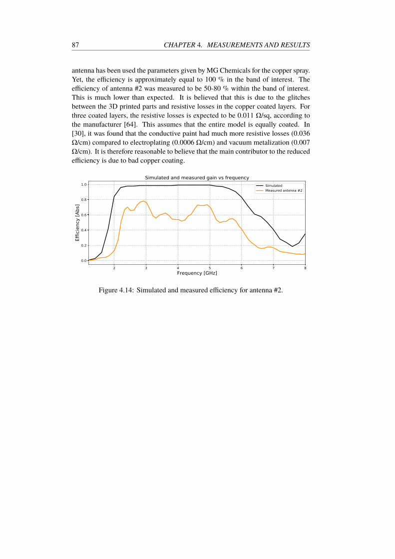
87 CHAPTER 4. MEASUREMENTS AND RESULTS
antenna has been used the parameters given by MG Chemicals for the copper spray.
Yet, the efficiency is approximately equal to 100 % in the band of interest. The
efficiency of antenna #2 was measured to be 50-80 % within the band of interest.
This is much lower than expected. It is believed that this is due to the glitches
between the 3D printed parts and resistive losses in the copper coated layers. For
three coated layers, the resistive losses is expected to be 0.011 Ω/sq, according to
the manufacturer [64]. This assumes that the entire model is equally coated. In
[30], it was found that the conductive paint had much more resistive losses (0.036
Ω/cm) compared to electroplating (0.0006 Ω/cm) and vacuum metalization (0.007
Ω/cm). It is therefore reasonable to believe that the main contributor to the reduced
efficiency is due to bad copper coating.
2 3 4 5 6 7 8Frequency [GHz]
0.0
0.2
0.4
0.6
0.8
1.0
Effic
ienc
y [A
bs]
Simulated and measured gain vs frequencySimulatedMeasured antenna #2
Figure 4.14: Simulated and measured efficiency for antenna #2.
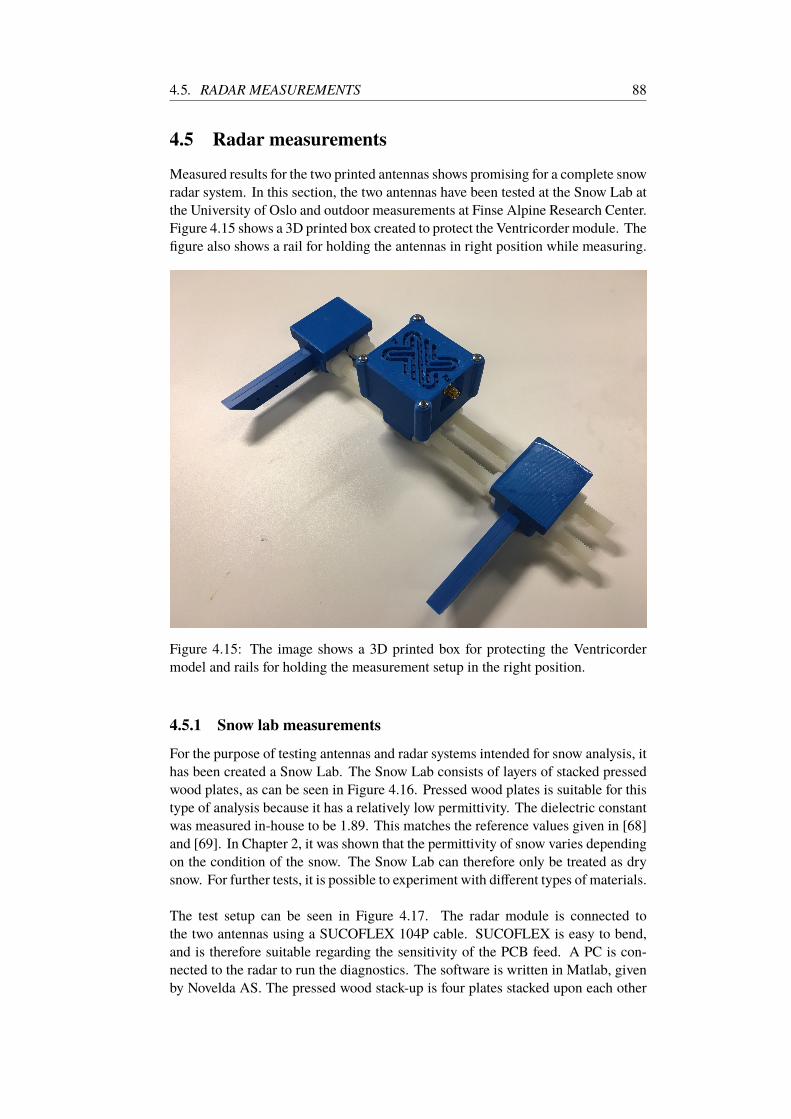
4.5. RADAR MEASUREMENTS 88
4.5 Radar measurements
Measured results for the two printed antennas shows promising for a complete snow
radar system. In this section, the two antennas have been tested at the Snow Lab at
the University of Oslo and outdoor measurements at Finse Alpine Research Center.
Figure 4.15 shows a 3D printed box created to protect the Ventricorder module. The
figure also shows a rail for holding the antennas in right position while measuring.
Figure 4.15: The image shows a 3D printed box for protecting the Ventricorder
model and rails for holding the measurement setup in the right position.
4.5.1 Snow lab measurements
For the purpose of testing antennas and radar systems intended for snow analysis, it
has been created a Snow Lab. The Snow Lab consists of layers of stacked pressed
wood plates, as can be seen in Figure 4.16. Pressed wood plates is suitable for this
type of analysis because it has a relatively low permittivity. The dielectric constant
was measured in-house to be 1.89. This matches the reference values given in [68]
and [69]. In Chapter 2, it was shown that the permittivity of snow varies depending
on the condition of the snow. The Snow Lab can therefore only be treated as dry
snow. For further tests, it is possible to experiment with different types of materials.
The test setup can be seen in Figure 4.17. The radar module is connected to
the two antennas using a SUCOFLEX 104P cable. SUCOFLEX is easy to bend,
and is therefore suitable regarding the sensitivity of the PCB feed. A PC is con-
nected to the radar to run the diagnostics. The software is written in Matlab, given
by Novelda AS. The pressed wood stack-up is four plates stacked upon each other
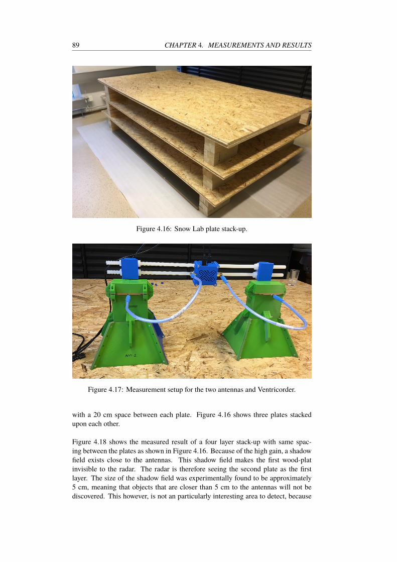
89 CHAPTER 4. MEASUREMENTS AND RESULTS
Figure 4.16: Snow Lab plate stack-up.
Figure 4.17: Measurement setup for the two antennas and Ventricorder.
with a 20 cm space between each plate. Figure 4.16 shows three plates stacked
upon each other.
Figure 4.18 shows the measured result of a four layer stack-up with same spac-
ing between the plates as shown in Figure 4.16. Because of the high gain, a shadow
field exists close to the antennas. This shadow field makes the first wood-plat
invisible to the radar. The radar is therefore seeing the second plate as the first
layer. The size of the shadow field was experimentally found to be approximately
5 cm, meaning that objects that are closer than 5 cm to the antennas will not be
discovered. This however, is not an particularly interesting area to detect, because

4.5. RADAR MEASUREMENTS 90
Figure 4.18: Reflected pulses from five plate stack-up measured in the Snow Lab.
one can simply analyze the top snow layer by hand.
Figure 4.19 shows the same results as was presented in Figure 4.18 plotted in
colors. The plot is placed besides the snow lab, and shows the distance between
each wood layer.
One interesting observation while measuring in the snow lab was that if an object
was placed inside one of the air gaps, the RF signal started to change direction. This
may be a problem in an outdoor measurements where the ground is not uniform
over the entire measuring area. If a rock lays beneath the snow, one may experience
that non of the transmitted signal will return.
4.5.2 Field measurements
The field measurements has been carried out at Finse Alpine Research Center,
Norway in March, 2017. The purpose of the trip was to get outdoor measurements
of the snow using the radar system. To get Real-Aperture Radar (RAR) images a
sled for carrying the radar system was made. The radar sled can be seen in Figure
4.20. A box on the back of the sled was created to protect the system from snow
and water.
Three different tests were planed to be performed in the field. The first test was to

91 CHAPTER 4. MEASUREMENTS AND RESULTS
Figure 4.19: The reflected signal plotted in colors, placed beside the snow lab.
Figure 4.20: Reflected pulses from five plate stack-up measured in the Snow Lab.
send one single pulse down into the snow in order to get reflections from each layer.
This test is some what similar to the test performed in the lab. The second test was
to place the radar at one location and take one measurement for each frequency
selection available for the radar. The third and last test, was to perform a RAR
analysis over a distance of 75 meters with measurement every second meter. Unfor-
tunately during the field measurement, the microcontroller unit on the Ventricorder
module failed. Necessary equipment for re-flashing the Atmel microcontroller was
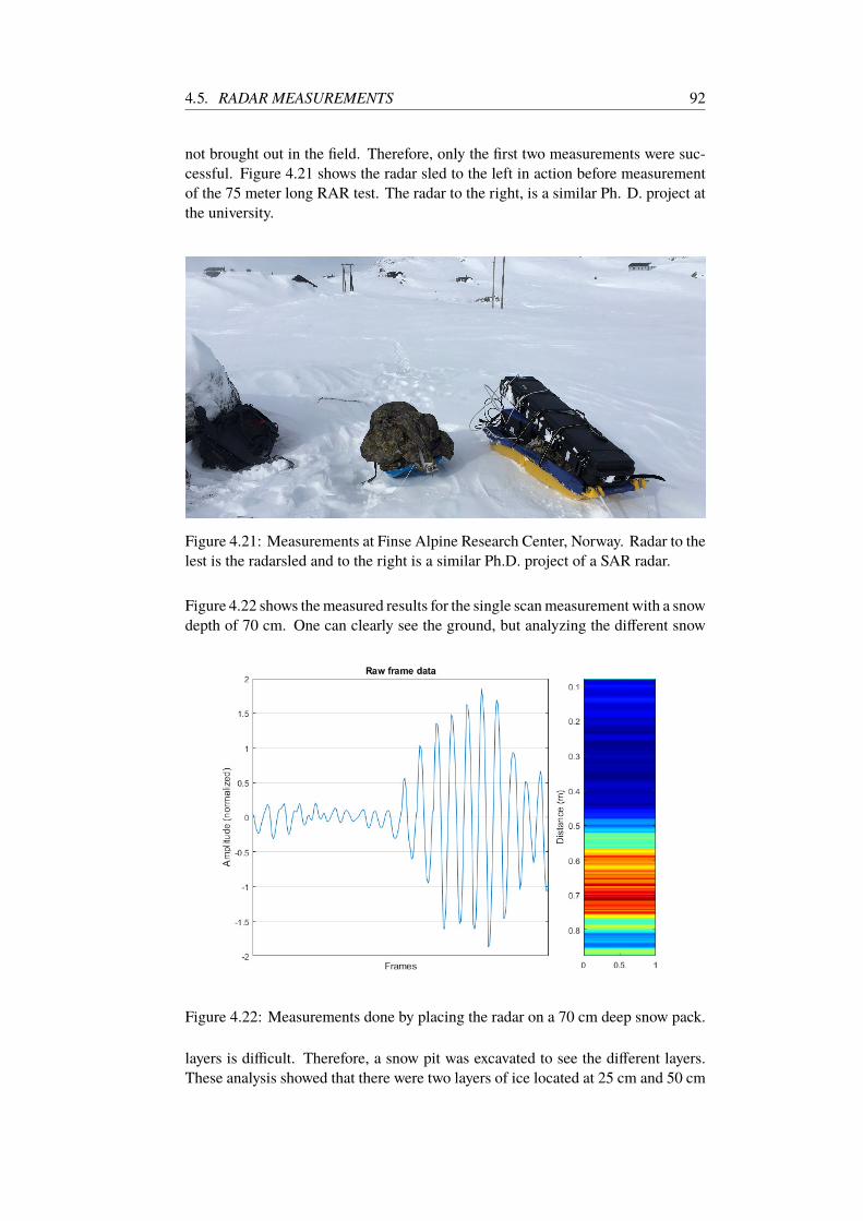
4.5. RADAR MEASUREMENTS 92
not brought out in the field. Therefore, only the first two measurements were suc-
cessful. Figure 4.21 shows the radar sled to the left in action before measurement
of the 75 meter long RAR test. The radar to the right, is a similar Ph. D. project at
the university.
Figure 4.21: Measurements at Finse Alpine Research Center, Norway. Radar to the
lest is the radarsled and to the right is a similar Ph.D. project of a SAR radar.
Figure 4.22 shows the measured results for the single scan measurement with a snow
depth of 70 cm. One can clearly see the ground, but analyzing the different snow
Figure 4.22: Measurements done by placing the radar on a 70 cm deep snow pack.
layers is difficult. Therefore, a snow pit was excavated to see the different layers.
These analysis showed that there were two layers of ice located at 25 cm and 50 cm
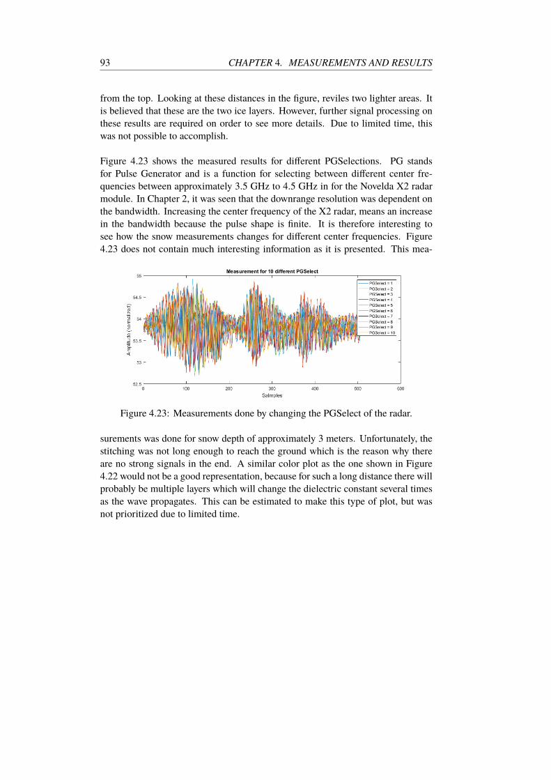
93 CHAPTER 4. MEASUREMENTS AND RESULTS
from the top. Looking at these distances in the figure, reviles two lighter areas. It
is believed that these are the two ice layers. However, further signal processing on
these results are required on order to see more details. Due to limited time, this
was not possible to accomplish.
Figure 4.23 shows the measured results for different PGSelections. PG stands
for Pulse Generator and is a function for selecting between different center fre-
quencies between approximately 3.5 GHz to 4.5 GHz in for the Novelda X2 radar
module. In Chapter 2, it was seen that the downrange resolution was dependent on
the bandwidth. Increasing the center frequency of the X2 radar, means an increase
in the bandwidth because the pulse shape is finite. It is therefore interesting to
see how the snow measurements changes for different center frequencies. Figure
4.23 does not contain much interesting information as it is presented. This mea-
Figure 4.23: Measurements done by changing the PGSelect of the radar.
surements was done for snow depth of approximately 3 meters. Unfortunately, the
stitching was not long enough to reach the ground which is the reason why there
are no strong signals in the end. A similar color plot as the one shown in Figure
4.22 would not be a good representation, because for such a long distance there will
probably be multiple layers which will change the dielectric constant several times
as the wave propagates. This can be estimated to make this type of plot, but was
not prioritized due to limited time.

4.6. SUMMARY OF ALL RESULTS 94
4.6 Summary of all results
In this chapter, the results for the final antennas has been presented. It was seen
in the first section that the printed waveguide did not performer very well. How-
ever, the concept of the PCB feed solution was shown to be promising. One other
interesting observation obtained form the waveguide measurements, was that the
performance between the low cost PLA and the expensive VeroClear was negligible,
in fact it was more difficult to work with the VeroClear model. This is beneficial
regarding simplicity and cost. Instead of using professional 3D printers, one can
simply use a hobby printer.
In the next section, the performance of the 3D printed antennas was shown and
discussed. It was seen that the performance matches the simulated quite good. It is
reasonable to believe that the mismatch is caused by mechanical challenges. More
on this discussion will be presented in the next chapter.
In the last section, lab- and outdoor measurements were presented. In the lab,
the radar system was able to detect each wood layers, which was seen in Figure
4.19. Also, outdoor measurements has been presented, but this data needs further
verification by signal processing.
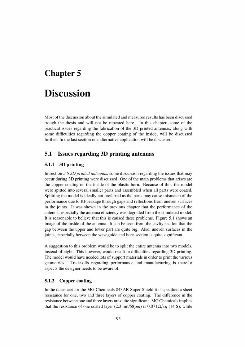
Chapter 5
Discussion
Most of the discussion about the simulated and measured results has been discussed
trough the thesis and will not be repeated here. In this chapter, some of the
practical issues regarding the fabrication of the 3D printed antennas, along with
some difficulties regarding the copper coating of the inside, will be discussed
further. In the last section one alternative application will be discussed.
5.1 Issues regarding 3D printing antennas
5.1.1 3D printing
In section 3.6 3D printed antennas, some discussion regarding the issues that may
occur during 3D printing were discussed. One of the main problems that arises are
the copper coating on the inside of the plastic horn. Because of this, the model
were spitted into several smaller parts and assembled when all parts were coated.
Splitting the model is ideally not preferred as the parts may cause mismatch of the
performance due to RF leakage through gaps and reflections from uneven surfaces
in the joints. It was shown in the previous chapter that the performance of the
antenna, especially the antenna efficiency was degraded from the simulated model.
It is reasonable to believe that this is caused these problems. Figure 5.1 shows an
image of the inside of the antenna. It can be seen from the cavity section that the
gap between the upper and lower part are quite big. Also, uneven surfaces in the
joints, especially between the waveguide and horn section is quite significant.
A suggestion to this problem would be to split the entire antenna into two models,
instead of eight. This however, would result in difficulties regarding 3D printing.
The model would have needed lots of support materials in order to print the various
geometries. Trade-offs regarding performance and manufacturing is therefor
aspects the designer needs to be aware of.
5.1.2 Copper coating
In the datasheet for the MG Chemicals 843AR Super Shield it is specified a sheet
resistance for one, two and three layers of copper coating. The difference in the
resistance between one and three layers are quite significant. MG Chemicals implies
that the resistance of one coated layer (2.3 mil/58µm) is 0.071Ω/sq (14 S), while
95
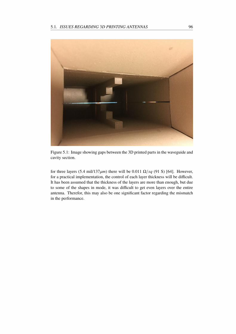
5.1. ISSUES REGARDING 3D PRINTING ANTENNAS 96
Figure 5.1: Image showing gaps between the 3D printed parts in the waveguide and
cavity section.
for three layers (5.4 mil/137µm) there will be 0.011 Ω/sq (91 S) [64]. However,
for a practical implementation, the control of each layer thickness will be difficult.
It has been assumed that the thickness of the layers are more than enough, but due
to some of the shapes in mode, it was difficult to get even layers over the entire
antenna. Therefor, this may also be one significant factor regarding the mismatch
in the performance.
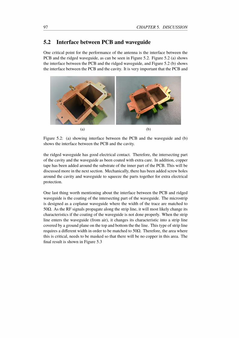
97 CHAPTER 5. DISCUSSION
5.2 Interface between PCB and waveguide
One critical point for the performance of the antenna is the interface between the
PCB and the ridged waveguide, as can be seen in Figure 5.2. Figure 5.2 (a) shows
the interface between the PCB and the ridged waveguide, and Figure 5.2 (b) shows
the interface between the PCB and the cavity. It is very important that the PCB and
(a) (b)
Figure 5.2: (a) showing interface between the PCB and the waveguide and (b)
shows the interface between the PCB and the cavity.
the ridged waveguide has good electrical contact. Therefore, the intersecting part
of the cavity and the waveguide as been coated with extra care. In addition, copper
tape has been added around the substrate of the inner part of the PCB. This will be
discussed more in the next section. Mechanically, there has been added screw holes
around the cavity and waveguide to squeeze the parts together for extra electrical
protection.
One last thing worth mentioning about the interface between the PCB and ridged
waveguide is the coating of the intersecting part of the waveguide. The microstrip
is designed as a coplanar waveguide where the width of the trace are matched to
50Ω. As the RF signals propagate along the strip line, it will most likely change its
characteristics if the coating of the waveguide is not done properly. When the strip
line enters the waveguide (from air), it changes its characteristic into a strip line
covered by a ground plane on the top and bottom the the line. This type of strip line
requires a different width in order to be matched to 50Ω. Therefore, the area where
this is critical, needs to be masked so that there will be no copper in this area. The
final result is shown in Figure 5.3
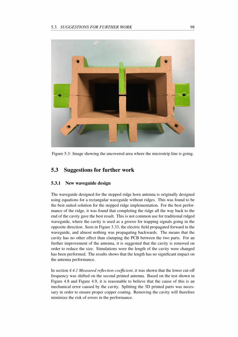
5.3. SUGGESTIONS FOR FURTHER WORK 98
Figure 5.3: Image showing the uncovered area where the microstrip line is going.
5.3 Suggestions for further work
5.3.1 New waveguide design
The waveguide designed for the stepped ridge horn antenna is originally designed
using equations for a rectangular waveguide without ridges. This was found to be
the best suited solution for the stepped ridge implementation. For the best perfor-
mance of the ridge, it was found that completing the ridge all the way back to the
end of the cavity gave the best result. This is not common use for traditional ridged
waveguide, where the cavity is used as a groove for trapping signals going in the
opposite direction. Seen in Figure 3.33, the electric field propagated forward in the
waveguide, and almost nothing was propagating backwards. The means that the
cavity has no other effect than clamping the PCB between the two parts. For an
further improvement of the antenna, it is suggested that the cavity is removed on
order to reduce the size. Simulations were the length of the cavity were changed
has been performed. The results shows that the length has no significant impact on
the antenna performance.
In section 4.4.1 Measured reflection coefficient, it was shown that the lower cut-off
frequency was shifted on the second printed antenna. Based on the test shown in
Figure 4.8 and Figure 4.9, it is reasonable to believe that the cause of this is an
mechanical error caused by the cavity. Splitting the 3D printed parts was neces-
sary in order to ensure proper copper coating. Removing the cavity will therefore
minimize the risk of errors in the performance.
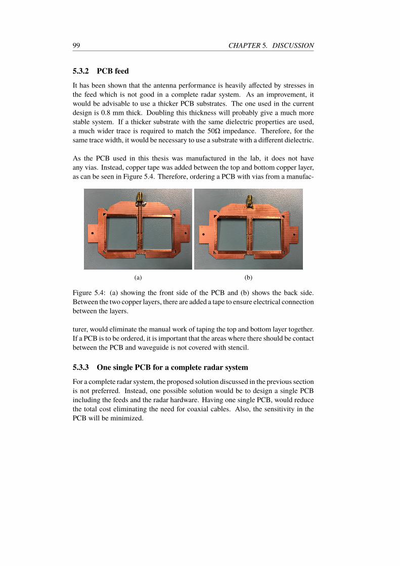
99 CHAPTER 5. DISCUSSION
5.3.2 PCB feed
It has been shown that the antenna performance is heavily affected by stresses in
the feed which is not good in a complete radar system. As an improvement, it
would be advisable to use a thicker PCB substrates. The one used in the current
design is 0.8 mm thick. Doubling this thickness will probably give a much more
stable system. If a thicker substrate with the same dielectric properties are used,
a much wider trace is required to match the 50Ω impedance. Therefore, for the
same trace width, it would be necessary to use a substrate with a different dielectric.
As the PCB used in this thesis was manufactured in the lab, it does not have
any vias. Instead, copper tape was added between the top and bottom copper layer,
as can be seen in Figure 5.4. Therefore, ordering a PCB with vias from a manufac-
(a) (b)
Figure 5.4: (a) showing the front side of the PCB and (b) shows the back side.
Between the two copper layers, there are added a tape to ensure electrical connection
between the layers.
turer, would eliminate the manual work of taping the top and bottom layer together.
If a PCB is to be ordered, it is important that the areas where there should be contact
between the PCB and waveguide is not covered with stencil.
5.3.3 One single PCB for a complete radar system
For a complete radar system, the proposed solution discussed in the previous section
is not preferred. Instead, one possible solution would be to design a single PCB
including the feeds and the radar hardware. Having one single PCB, would reduce
the total cost eliminating the need for coaxial cables. Also, the sensitivity in the
PCB will be minimized.

5.4. ALTERNATIVE RADAR APPLICATIONS 100
5.4 Alternative radar applications
The main application that has been discussed though this thesis, is imaging of the
snow profile to map the potential risk of snow avalanches. One other important
discussion is to use radar for human detection in a snow avalanche. There excises
few products on the marked that are efficient for detecting buried humans. One
solution is the Snow Scan Rescue Radar from Sensors & Software [70], but this
system needs movement from the person in order to be detected. Besides the use of
radar the most efficient technique the avalanche beacon, but this only works if the
affected person have a his or hear own beacon.
Using the presented design on a snow stick, it can easily be carried out on the
avalanche area and create RAR images. After a snow avalanche, the snow will be
hard and compact, so the dielectric properties will probably be equal for the hole
snow pack. Therefore, human detection may be possible.
Chapter 6
Conclusion
This thesis present the design and measurements of two 3D printed stepped ridge
horn antennas, suitable for snow imaging and remote Geo-Sensing applications.
The antennas have been characterized for air due to small changes between air and
dry snow, as have been discussed in Chapter 2. The design specifications were
derived based on the requirements for ultra-wideband, high gain antennas required
for directive beam measurement of the snow. Modeling and simulations has been
performed using Ansys HFSS and the characterization has been performed at the
anechoic chamber at the Department of Informatics, University of Oslo.
The presented design is a stepped ridge horn antenna which has been charac-
terized for large bandwidth in the range 2.4 GHz to 6.1 GHz with a high gain over
the entire area. Measured results shows that the gain varies between 10 dBi and 15
dBi within this antenna bandwidth. At center frequency (4 GHz), the peak gain was
measured to be 12.6 dBi and 12 dBi for antenna #1 and antenna #2, respectively.
The measured half-power beamwidth of antenna #1 is 26 in the E-plane and 26
in the H-plane at 4 GHz. For antenna #2 the measured half-power beamwidth is
24 and 28. Measured front-to-back ratio is 22 dB and 24 dB for antenna #1 and
antenna #2, respectively.
The feeding technique for the 3D printed waveguide is proposed by new PCB
microstrip solution, replacing the traditional coaxial probe feed solution. The per-
formance of the PCB feed matches the probe feed, as was seen in section 3.4 A
new method for feeding plastic waveguide. The work in this feeding technique
has been submitted to the IEEE MTT-S International Microwave Workshop Series
on Advanced Materials and Processes (IMWS-AMP) conference (see Appendix A).
The measured results for the antenna has a relatively good match to the simu-
lated, and it is believed that the mismatch is due to mechanical challenges and
uneven copper coating of the plastic surface. Referring to Figure 4.8 and Figure
4.9, it was seen the cavity of the first printed antenna shifted up the lower cut-
off frequency approximately 800 MHz when it was used together with the second
printed antenna. This is believed to be differences in the two 3D printed models.
In Chapter 5 that gaps between the 3D printed parts was shown to be remarkable.
Also, the same two figures showed that the PCB was highly exposed to mechani-
101

102
cal stress. As a further improvement it has been suggested to use a thicker substrate.
Measurements has been performed together with the Novelda X2 Ventricorder
module at the university Snow Lab. Also, outdoor measurements at Finse Alpine
Research Center has been performed. Based on the measurements, it is believed
that the radar are able to distinguish between different snow layers. However, more
signal processing needs to be performed to verify this.

Bibliography
[1] L. Dawson. (Sep. 2014). Avatech electronic snow profile sensor & data
network, [Online]. Available: https://www.wildsnow.com/14505/avatech-
smartphone-app-probe-sp1/ (visited on 05/10/2017).
[2] N. A. (2010). N.a., [Online]. Available: https: / /www.polartrec.com/files/
members/katey-shirey/images/img5510.jpg (visited on 04/19/2017).
[3] “IEEE Standard Letter Designations for Radar-Frequency Bands”, IEEE Std.
521-2002, pp. 1–10, 2002. doi: 10.1109/IEEESTD.2003.94224.
[4] Novelda AS. (2015). Xethru x2, [Online]. Available: https: / /www.xethru.
com/x2-uwb-radar-chip.html/ (visited on 04/19/2017).
[5] M. A. Richards, Fundamentals of radar signal processing, 2nd ed. USA:
Mc. Graw Hill, 2014.
[6] D. J. Daniels, “Ground penetrating radar”, in, D. J. Daniels, Ed., 2nd
ed. London, UK: The Institution of Electrical Engineers, 2004, ch. 1.
Introduction, pp. 1–11.
[7] Wikipedia. (May 2017). History of radar, [Online]. Available: https:/ / en.
wikipedia.org/wiki/History_of_radar#Christian_H.C3.BClsmeyer (visited on
05/13/2017).
[8] H. C. D. Prospector Inst Fuer Praktisch Geol, “Verfahren zur elektrischen
bodenerforschung (a method for electrical ground exploration)”, German,
Patent DE489434 C, Jan. 1930. [Online]. Available: https:/ /www.google.
com/patents/DE489434C?cl=en.
[9] A. P. Annan, Ground Penetrating Radar Principles, Procedures &
Applications, 1st ed. Mississauga, Canada: Sensors & Software Inc., 2003.
[10] varsom.no. (2017). Snøskredulykker- og hendelser, [Online]. Available: http:
/ / www . varsom . no / ulykker / snoskredulykker - og - hendelser/ (visited on
05/13/2017).
[11] J. Floyer. (Dec. 2016). Backcountry conditions, [Online]. Available: http:
/ / powdercanada . com / 2016 / 12 / backcountry - conditions/ (visited on
05/06/2017).
[12] C. Wolff. (Nov. 1998). Radartutorial.eu, [Online]. Available: http : / / www.
radartutorial.eu/index.en.html (visited on 05/03/2017).
[13] F. T. Ulaby and D. G. Long, Microwave Radar and Radiometric Remote
Sensing. Ann Arbor, MI: The University of Michigan Press, 2014.
[14] S. Y. Huang, Loss tangent, Notes, Feb. 2012.
103

BIBLIOGRAPHY 104
[15] D. R. Kwok, Lossy medium, Lecture slides, Apr. 2015. [Online]. Available:
http://www.engr.sjsu.edu/rkwok/EE142/Lossy_Medium.pdf.
[16] T. M. Hallikainen, F. T. Ulaby, and M. Abdelrazik., “Modeling the dielectric
behavior of wet snow in 4-18 ghz range”, IEEE International Geoscience
and Remote Sensing Symposium, 31 August - 2 September 1983.
[17] T. M. Hallikainen, F. T. Ulaby, M. C. Dobson, and A. El-Rayes., “Dielectric
measurements of soils in the 3 to 37 ghz band between -50 c and 23 c”,
IEEE International Geoscience and Remote Sensing Symposium, 27 - 30
August 1984.
[18] T. M. Hallikainen, F. T. Ulaby, and M. Abdelrazik, “The dielectric properties
of snow in the 3 to 37 ghz range”, IEEE Transactions on Antennas and
Propagation, vol. 34(11), pp. 1329–1340, 1984.
[19] D. J. Daniels, “Ground penetrating radar”, in, D. J. Daniels, Ed., 2nd ed.
London, UK: The Institution of Electrical Engineers, 2004, ch. 2. System
Design, pp. 13–36.
[20] B. R. Mahafza, Radar Systems Analysis and Design Using MATLAB, 1st ed.
Huntsville, AL: Chapman & Hall/CRC, 2000.
[21] 3D Radar. (N.A.). Gpr technology, [Online]. Available: http : / / www. 3d -
radar.com/?page_id=939 (visited on 05/04/2017).
[22] M. I. Skolnik, Introduction to RADAR Systems, 3rd ed. Nagar, New Delhi:
McGraw-Hill, 2001.
[23] C. A. Balanis, “Modern antenna handbook”, in, C. A. Balanis, Ed., 1st ed.
Hoboken, NJ: John Wiley & Sons, 2008, ch. 1. Fundamental Parameters and
Definitions for Antennas, pp. 3–56.
[24] Sensors & Softwares. (). Pulseekko, [Online]. Available: https://www.sensoft.
ca/products/pulseekkopro/overview/ (visited on 05/02/2017).
[25] National Avalanche Center. (N. A.). Starting zone the portion of an avalanche
path where an avalanche releases., [Online]. Available: http : / / www .
fsavalanche.org/starting-zone/ (visited on 05/02/2017).
[26] National Avalanche Center. (N. A.). A snowpack stratum differentiated from
others by weather, metamorphism, or other processes., [Online]. Available:
http://www.fsavalanche.org/layer-snow/ (visited on 05/02/2017).
[27] S. Greffin and T. Pippett, “Ground penetrating radar”, Geophysical and
Remote Sensing Methods for Regolith Exploration (CRCLEME), vol. 144,
pp. 80–89, 2002.
[28] J. Lux. (2000). Soil dielectric properties, [Online]. Available: http://pe2bz.
philpem . me . uk / Comm/ - %5C % 20Antenna / Info - 905 - Misc / soildiel . htm
(visited on 05/05/2017).
[29] S.-. E. Hamran, “Ground penetrating radar”, in, D. J. Daniels, Ed., 2nd ed.
London, UK: The Institution of Electrical Engineers, 2004, ch. 11.4. GPR
sounding of polythermal glaciers, pp. 455–460.
105 BIBLIOGRAPHY
[30] K. V. Hoel, S. Kristoffersen, J. Moen, K. G. Kjelgård, and T. S. Lande,
“Broadband antenna design using different 3d printing technologies and
metallization processes”, 10th European Conference on Antennas and
Propagation (EuCAP), pp. 1–5, 2016.
[31] V. Midtbøen, K. G. Kjelgård, and T. S. Lande, “3d printed horn antenna
with pcb microstrip feed for uwb radar applications”, Progress in IEEE
MTT-S International Microwave Workshop Series on Advanced Materials
and Processes (IMWS-AMP), 2017.
[32] Wikipedia. (Apr. 2017). Parabolic antenna, [Online]. Available: https://en.
wikipedia.org/wiki/Parabolic_antenna (visited on 05/02/2017).
[33] H. Schantz, The Art and Science of Ultrawideband Antenna, 2nd ed.
Norwood, MA: Artech House, 2015.
[34] J. Huang, “Modern antenna handbook”, in, C. A. Balanis, Ed., 1st ed.
Hoboken, NJ: John Wiley & Sons, 2008, ch. 4. Microstrip Antennas:
Analysis, Design, and Applications, pp. 97–156.
[35] A. De, C. K. Chosh, and A. K. Bhattacherjee, “Design and performance
analysis of microstrip patch array antennas with different configurations”,
International Journal of Future Generation Communication and Networking,
vol. 9(3), pp. 97–101, 2016.
[36] W. F. Croswell, T. Durham, M. Jones, D. Schaubert, P. Friederich, and
J. G. Maloney, “Modern antenna handbook”, in, C. A. Balanis, Ed., 1st ed.
Hoboken, NJ: John Wiley & Sons, 2008, ch. 12: Wideband Arrays, pp. 581–
629.
[37] R. C. Tylor, B. A. Munk, and T. E. Durham, “Wideband phased array antenna
and associated methods”, United States, Patent US6512487 B1, Jan. 2003.
[Online]. Available: https://www.google.com/patents/US6512487.
[38] D. T. Emerson. (1998). The work of jagadis chandra bose: 100 years of mm-
wave research, [Online]. Available: https://www.cv.nrao.edu/~demerson/
bose/bose.html (visited on 05/01/2017).
[39] S. A. Schelkunoff and H. T. Friis, Antennas: Theory and Practice, 1st ed.
NY, USA: John Wiley & Sons, Inc, 1952, Appendix VI.
[40] ETS-Lindgren, Emc antennas: Double-ridge waveguide horn, 2014.
[Online]. Available: http : / / www.ets - lindgren .com/ pdf / 3115 .pdf (visited
on 05/01/2017).
[41] S. J. Orfanidis, Electromagnetic Waves and Antennas, 1st ed. Rutgers
University: Sophocles J. Orfanidis, 2016.
[42] K. Blattenberger. (2017). Coaxial cable equations, [Online]. Available: http:
//www.rfcafe.com/references/electrical/coax.htm (visited on 05/07/2017).
[43] K. Blattenberger. (Sep. 2016). Rectangular & circular waveguide: Equations,
fields, & fco calculator, [Online]. Available: https : / / www . rfcafe . com /
references/electrical/waveguide.htm (visited on 09/05/2016).
[44] K. L. Walton and V. C. Sundberg, “Broadband ridged horn design”,
Microwave J., pp. 96–101, 1964.

BIBLIOGRAPHY 106
[45] W. H. Pickering et al., “Waveguide handbook”, in, N. Marcuvitz, Ed., 1th
ed. New York, NY: Dover Publications, 1951, ch. 8. Composite Structures,
pp. 387–413.
[46] C. Granet, G. L. James, and A. R. Forsyth, “Modern antenna handbook”, in,
C. A. Balanis, Ed., 1st ed. Hoboken, NJ: John Wiley & Sons, 2008, ch. 3.
Aperture Antennas: Waveguides and Horns, pp. 157–200.
[47] J. J. Carr and G. W. Hippisley, Practical Antenna Handbook, 5th ed. USA:
McGraw-Hill Companies, 2012, pp. 447–489.
[48] MicrowaveTools.com. (Dec. 2016). Pin-fed pyramidal horn, [Online].
Available: http://www.microwavetools.com/pin-fed-pyramidal-horn/ (visited
on 12/19/2016).
[49] S. Hopfer, “The design of ridged waveguides”, IRE Transactions on
Microwave Theory and Techniques, vol. 3, pp. 20–29, 1955.
[50] T. S. Bird and A. W. Love, “Antenna engineering handbook”, in, J. L. Volakis,
Ed., 4th ed. Upper Saddle River, NJ: McGraw-Hill Education, 2004, ch. 14.
Horn Antennas.
[51] Y. Yang, Y. Wang, and A. E. Fathy, “Design of compact vivaldi antenna
arrays for uwb see through wall applications”, Progress In Electromagnetic
Research (PIER), vol. 82, pp. 401–418, 2008.
[52] F. Karshenas, A. R. Mallahzadeh, and A. Imani, “Modified tem horn
antenna for wideband applications”, International Symposium on Antenna
Technology and Applied Electromagnetics and the Canadian Radio Science
Meeting, pp. 1–5, 2009.
[53] C. Sarkar, “Some parametric studies of vivaldi antenna”, International
Journal of u- and e- Service, Science and Technology, vol. 7, pp. 323–
328, 2014.
[54] T. A. Milligan, Modern Antenna Design, 2nd ed. Hoboken, NJ: John Wiley
& Sons, 2005, pp. 356–372.
[55] B. Majumdar, D. Baer, S. Chakraborty, K. P. Esselle, and M. Heimlich,
“Advantages and limitations of 3d printing a dual-ridged horn antenna”,
Microwave and Optical Technology Letters, vol. 58, pp. 2110–2117, 2016.
[56] J.-C. S. Chieh, B. Dick, S. Loui, and J. D. Rockway, “Development of a ku-
band corrugated conical horn using 3-d print technology”, IEEE Antennas
and Wireless Propagation Letters, vol. 13, pp. 201–204, 2014.
[57] E. Pucci, E. R. Iglesias, J. L. V. Roy, and P.-S. Kildal, “Planar dual-mode horn
array with corporate-feed network in inverted microstrip gap waveguide”,
IEEE Transactions on Antennas and Propagation (SUBMITTED), vol. 62(7),
pp. 3534–3542, 2014.
[58] D. M. Pozar, Microwave Engineering, 4th ed. USA: John Wiley & Sons,
2012, pp. 261–267.
[59] Y. Zhou, E. Li, G.-F. Guo, T. Yang, and L. Liu, “Design of millimeter wave
wideband transition from double-ridge waveguide to coax line”, J Infrared
Milli Terahz Waves, vol. 32, pp. 26–33, 2011.

107 BIBLIOGRAPHY
[60] Antenna Magus. (2012). Coax to dual-ridged rectangular waveguide
transition, [Online]. Available: http://www.antennamagus.com/database/
antennas/antenna_page.php?id=304 (visited on 02/14/2017).
[61] S. B. Cohn, “Properties of ridge wave guide”, Proceedings of the IRE,
vol. 35(8), pp. 783–788, 1947.
[62] A. H. Systems, SAS-571 Double Ridge Guide Horn Antenna. [Online].
Available: http : / / www . ahsystems . com / datasheets / SAS - 571 _ Horn _
Antenna_Datasheet.pdf (visited on 03/08/2017).
[63] E. Huber, M. Mirzaee, J. Bjorgaard, M. Hoyak, S. Noghanian, and I. Chang,
“Dielectric property measurement of pla”, Electro Information Technology
(EIT), 2016 IEEE International Conference on, pp. 0788–0792, 2016.
[64] MG Chemicals, Super shield silver coated copper conductive coating 843ar
technical data sheet, 2017. [Online]. Available: http://www.mgchemicals.
com/downloads/tds/tds-843ar-l.pdf (visited on 03/12/2017).
[65] Wikipedia. (Mar. 2017). Fused deposition modeling, [Online]. Available:
https : / / en . wikipedia . org / wiki / Fused _ deposition _ modeling (visited on
04/20/2017).
[66] C. R. Garcia, R. C. Runpf, H. H. Tsang, and J. H. Barton, “Effects of
extreme surface roughness on 3d printed horn antenna”, Electronics Letters,
vol. 49(12), pp. 1–2, 2013.
[67] Stratasys Ltd, Veroclear (rgd810), 2016. [Online]. Available: https://goo.gl/
pYn40M (visited on 03/12/2017).
[68] C. Thajudeen, A. Hoorfar, and F. Ahmad, “Measured complex permittivity
of walls with different hydration levels and the effect on power estimation
of twri target returns”, Progress In Electromagnetics Research B, vol. 30,
pp. 177–199, 2011.
[69] Clipper Controls. (2017). Dielectric constant values, [Online]. Available:
http : / / www. clippercontrols . com / pages / Dielectric - Constant - Values . html
(visited on 04/26/2017).
[70] Sensors & Software. (N. A.). Snowscan overview, [Online]. Available: https:
//www.sensoft.ca/products/snowscan/overview/ (visited on 05/13/2017).

BIBLIOGRAPHY 108

Appendices
109


Appendix A
Paper
The following paper has been submitted to the “IEEE MTT-S International
Microwave Workshop Series on Advanced Materials and Processes (IMWS-AMP)
conference” Acceptance status is as of this writing not yet known.
111
3D Printed Horn Antenna with PCB Microstrip
Feed for UWB Radar Applications
Vegard Midtbøen, Kristian G. Kjelgard, Tor S. LandeDepartment of Informatics,University of Oslo, Norway
Email: [email protected], kristigk,[email protected]
Abstract—In this paper, a 3D printed Double Ridge HornAntenna (DRHA) for mobile snow cover monitoring is presented.The DRHA is designed for high bandwidth and high gain asrequired for a pulsed radar system. The bandwidth is between2.4 and 5.1 GHz with an in-band gain between 12 to 14 dBi.The antenna parts are fabricated with a standard 3D printerusing light-weighted plastic material (PLA). The surface is coppercoated on the inside adding conductivity. A PCB plate is insertedas feed for 3D printed plastic waveguides replacing traditionalcoaxial probe feed. The antenna has a total weight of less than400g and the total cost is about $60. Both cost and weight issignificantly lower than commercially available DRHAs addingfast and easy prototyping. Low weight, high gain and largebandwidth makes this antenna suitable for mobile systems likesnow cover analysis.
I. INTRODUCTION
In applications where low weight, geometric flexibility
as well as low cost is desired, 3D printed antennas may
offer advantages where machined, metal antenna fall short.
Surprisingly good performance is attainable with easy and
fast prototyping. Typically, in mobile applications like Un-
manned Aerial Vehicles (UAV) light weight antennas are
desired and may even be integrated as an integral mechanical
part of the mobile platform [1]. However, challenges exist
fabricating antennas in plastic materials like proper conductive
coating, mechanical stability and robustness. Still, our initial
experiments are promising although somewhat different design
procedures are required.
In countries with snow covered mountains, snow cover
assessment is important especially for snow avalanche risk
determination. Today fairly manual time-consuming methods
are used like digging a pit in the snow or inserting a pole
in the snow pack and sense the mechanical resistance. Due
to very few real observations risk assessment is both difficult
and inaccurate. In order to increase observation density, better,
faster and more observations are desired. Our project is to
bring forward an electronic ”pole” for snow assessment using
a miniaturized radar system. A mobile radar beam is looking
downwards into the snow pack and continuously measuring
while dragging a radar-sled over the terrain.
Our snow assessment radar sled is built around a single
chip CMOS, UWB radar [2]. For proper radar SAR imaging
resolution, a center frequency of 4 GHz with a signal band-
width of 1.5 GHz is adopted. A key component for proper
operation is antennas adding gain and focus. Aiming for high
gain some sort of horn derivative antenna architecture should
provide desired performance, but commercially available horns
are expensive, heavy and some add significant dispersion
degrading performance.
3D printing technology has made low cost high-quality
mechanical prototyping fast and easy. The consumer/semi-pro
3D printer market is dominated by simple Fused deposition
modelling (FDM) machines using low cost thermoplastic
polymers (ABS, PLA). Various metallization processes of
3D printed microwave components such as electroplating and
spray painting may add conductive surfaces [3], [4]. In [3] an
original antenna in aluminium was compared with a 3D printed
copy using electroplating and metal spray paint. Radiation
pattern and reflection coefficient of the original and 3D printed
antenna matched within the measurement error proving the
feasibility of 3D printed horn antennas. Still further refinement
is required towards the interface between 3D printed parts and
RF source. Traditional coaxial feeds with SMA connector are
expensive, heavy and less compatible with 3D printed parts
requiring soldering or mechanical fixture [5], [6]. In addition,
special considerations are required for robust operation of 3D
printed feed structures.
In this paper, we propose a new DRHA design optimized for
snow radar assement. The antenna is 3D printed and metallized
with conductive spray. A transmission line implemented on a
Printed Circuit Board (PCB) line directly feeding the antenna
ridges.
II. DESIGN
DRHA are often designed for maximum bandwidth by
tapering the ridges from the bottom of the feed to the
horn edge, even extended outside the horn. Conventional
tapering trades very wide bandwidth match for non-linear
gain severely distorting the wideband pulse transmitted. To
widen the bandwidth of un-ridged horns without sacrificing the
gain at lower frequency we designed a new tapering profile.
By stepping the ridge down to the horn surface inside the
waveguide section, the impedance matching is maintained over
the required bandwidth with flat gain. The dimensions of
the desired waveguide is determined from [7]. For a cut-off
frequency of fc = 2 GHz and a center frequency of f0 = 4
GHz, width a = 74.95 mm and hight b = 37.47 mm is required.
The size of each step is shown in Fig. 1.
Raising the impedance from 50 Ω signal to 377 Ω air within
the waveguide will take advantage of the high gain provided by
the horn aperture. The dimensions of the horn aperture can be
112
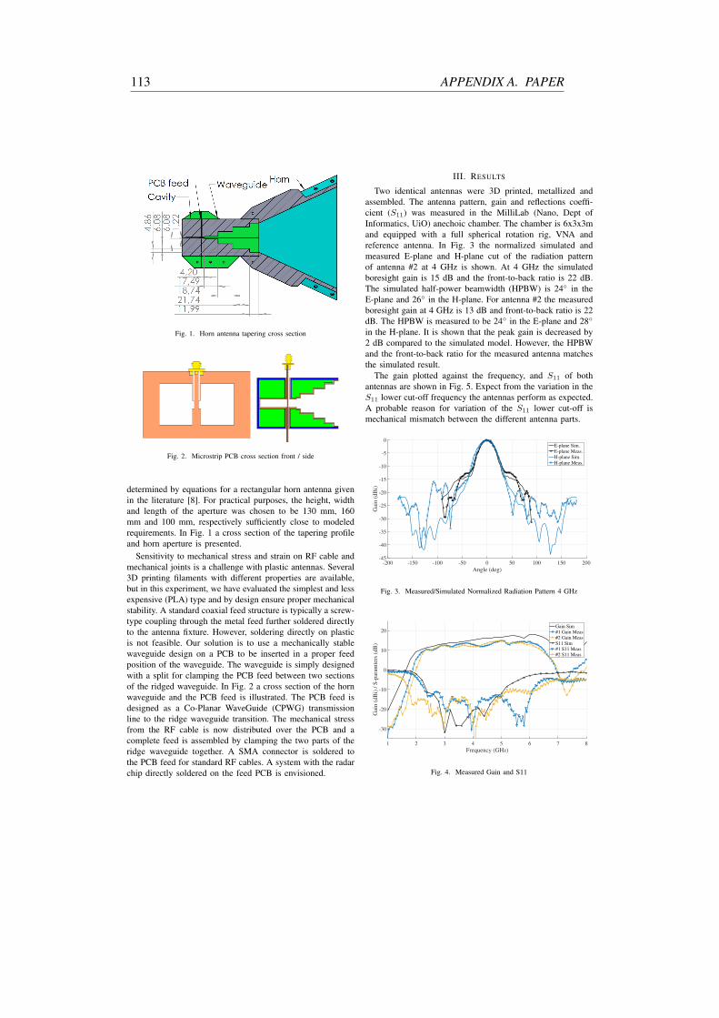
Fig. 1. Horn antenna tapering cross section
Fig. 2. Microstrip PCB cross section front / side
determined by equations for a rectangular horn antenna given
in the literature [8]. For practical purposes, the height, width
and length of the aperture was chosen to be 130 mm, 160
mm and 100 mm, respectively sufficiently close to modeled
requirements. In Fig. 1 a cross section of the tapering profile
and horn aperture is presented.
Sensitivity to mechanical stress and strain on RF cable and
mechanical joints is a challenge with plastic antennas. Several
3D printing filaments with different properties are available,
but in this experiment, we have evaluated the simplest and less
expensive (PLA) type and by design ensure proper mechanical
stability. A standard coaxial feed structure is typically a screw-
type coupling through the metal feed further soldered directly
to the antenna fixture. However, soldering directly on plastic
is not feasible. Our solution is to use a mechanically stable
waveguide design on a PCB to be inserted in a proper feed
position of the waveguide. The waveguide is simply designed
with a split for clamping the PCB feed between two sections
of the ridged waveguide. In Fig. 2 a cross section of the horn
waveguide and the PCB feed is illustrated. The PCB feed is
designed as a Co-Planar WaveGuide (CPWG) transmission
line to the ridge waveguide transition. The mechanical stress
from the RF cable is now distributed over the PCB and a
complete feed is assembled by clamping the two parts of the
ridge waveguide together. A SMA connector is soldered to
the PCB feed for standard RF cables. A system with the radar
chip directly soldered on the feed PCB is envisioned.
III. RESULTS
Two identical antennas were 3D printed, metallized and
assembled. The antenna pattern, gain and reflections coeffi-
cient (S11) was measured in the MilliLab (Nano, Dept of
Informatics, UiO) anechoic chamber. The chamber is 6x3x3m
and equipped with a full spherical rotation rig, VNA and
reference antenna. In Fig. 3 the normalized simulated and
measured E-plane and H-plane cut of the radiation pattern
of antenna #2 at 4 GHz is shown. At 4 GHz the simulated
boresight gain is 15 dB and the front-to-back ratio is 22 dB.
The simulated half-power beamwidth (HPBW) is 24 in the
E-plane and 26 in the H-plane. For antenna #2 the measured
boresight gain at 4 GHz is 13 dB and front-to-back ratio is 22
dB. The HPBW is measured to be 24 in the E-plane and 28
in the H-plane. It is shown that the peak gain is decreased by
2 dB compared to the simulated model. However, the HPBW
and the front-to-back ratio for the measured antenna matches
the simulated result.
The gain plotted against the frequency, and S11 of both
antennas are shown in Fig. 5. Expect from the variation in the
S11 lower cut-off frequency the antennas perform as expected.
A probable reason for variation of the S11 lower cut-off is
mechanical mismatch between the different antenna parts.
-200 -150 -100 -50 0 50 100 150 200
Angle (deg)
-45
-40
-35
-30
-25
-20
-15
-10
-5
0
Gai
n (
dB
i)
E-plane Sim.
E-plane Meas.
H-plane Sim.
H-plane Meas.
Fig. 3. Measured/Simulated Normalized Radiation Pattern 4 GHz
1 2 3 4 5 6 7 8
Frequency (GHz)
-30
-20
-10
0
10
20
Gai
n (
dB
i) /
S-p
aram
ters
(d
B)
Gain Sim
#1 Gain Meas
#2 Gain Meas
S11 Sim
#1 S11 Meas
#2 S11 Meas
Fig. 4. Measured Gain and S11
113 APPENDIX A. PAPER
A simple stress and strain test was performed comparing
two antennas variations. Interestingly enough, antenna #1
reacted more to PCB bending than antenna #2. By switching
the cavity between antennas, we observed that the two cavities
had different characteristics. The cavity for the antenna #1
increased the cut-off frequency for both antennas. These
variations are believed to originate from uneven surface of
mechanical parts and possibly also glitches.
1 2 3 4 5 6 7 8
Frequency (GHz)
0
0.2
0.4
0.6
0.8
1
Eff
icie
ncy
Sim
#2 Meas
Fig. 5. Antenna radiation efficiency
The efficiency of antenna #2 was measured to be 50-80 %.
We believe that this is caused by the glitches between the 3D
printed parts and resistive losses in the copper coated layers.
For three coated layers, the resistive losses is expected to be
0.011 Ω/sq, according to the manufacturer [9]. This assumes
that the entire model has uniformly coating covering (not easy
with manual spaying). In [3], it was found that the conductive
paint had much more resistive loss (0.036 Ω/cm) compared
to electroplating (0.0006 Ω/cm) and vacuum metallization
(0.007 Ω/cm). It is therefore expected that the efficiency
would decrease compared to the simulated model. In order
to reduce the risk of non uniform coating, the antenna has
been split into smaller models. Still uniform manual spraying
is difficult and probably the primary reason for degraded
efficiency.
Fig. 6 and Fig. 7 shows an image of the two 3D printed
horn antennas and a prototype of a snow cover radar inspec-
tion system. The antennas are printed in PLA plastic using
Ulimaker 3 and copper coated with the 843AR Super Shield
[9]. The system was tested at Finse Alpine Research Center,
Norway in March 2017.
Fig. 6. 3D printed horn antennas.
Fig. 7. Radar sled.
IV. CONCLUSION
A new 3D printed DRHA design is presented. A stepped
ridge inside the waveguide portion of the horn enable wide-
band impedance matching while maintaining the gain of the
non-ridged horn. With a measured gain of 12-14 dB from
2.3 to 6 GHz, symmetric radiation pattern and good match
the antenna provide the characteristics required in our snow
radar-sled. To reduce weight and cost of the antenna, Low-cost
3D printing technology combined with simple copper metal
spray is used. Compared to commercial metal antennas, cost
and weight is significantly reduced. A slightly lower efficiency
than expected is measured which is due to surface resistance
and glitches antenna parts. The PCB feed developed for 3D
printing is distributing mechanical stress and simplifying the
RF connection. A system with radar chip and antenna feed on
a single PCB is feasible for further development.
REFERENCES
[1] K. V. Hoel, S. Kristoffersen, J. Moen, G. Holm, and T. S. Lande,“Characterization of a 3d printed wideband waveguide and horn antennastructure embedded in a uav wing,” in 2016 10th European Conference
on Antennas and Propagation (EuCAP), April 2016, pp. 1–4.[2] N. AS, “X2 impulse radar transceiver,” 2014. [Online]. Available:
https://www.xethru.com/x2-uwb-radar-chip.html/[3] K. V. Hoel, S. Kristoffersen, J. Moen, K. G. Kjelgrd, and T. S. Lande,
“Broadband antenna design using different 3d printing technologies andmetallization processes,” in 2016 10th European Conference on Antennas
and Propagation (EuCAP), April 2016, pp. 1–5.[4] E. G. Geterud, P. Bergmark, and J. Yang, “Lightweight waveguide and
antenna components using plating on plastics,” in 2013 7th European
Conference on Antennas and Propagation (EuCAP), April 2013, pp.1812–1815.
[5] A. Prigaud, S. Bila, O. Tantot, N. Delhote, and S. Verdeyme, “3d printingof microwave passive components by different additive manufacturingtechnologies,” in 2016 IEEE MTT-S International Microwave Workshop
Series on Advanced Materials and Processes for RF and THz Applications
(IMWS-AMP), July 2016, pp. 1–4.[6] B. Majumdar, D. Baer, S. Chakraborty, K. P. Esselle, and M. Heimlich, “A
3d printed dual-ridged horn antenna,” in 2016 International Conference
on Electromagnetics in Advanced Applications (ICEAA), Sept 2016, pp.836–839.
[7] J. J. Carr and G. W. Hippisley, Practical Antenna Handbook, 5th ed.USA: McGraw-Hill Companies, 2012, pp. 370–383.
[8] G. L. J. C. Granet and A. R. Forsyth, Modern Antenna Handbook, 1st ed.Hoboken, NJ: John Wiley & Sons, 2008, ch. 3. Aperture Antennas:Waveguides and Horns, pp. 118–119.
[9] M. Chemicals, “Super shield silver coated copper conductivecoating 843ar technical data sheet,” 2017. [Online]. Available:http://www.mgchemicals.com/downloads/tds/tds-843ar-l.pdf
114

Appendix B
Machine drawings
Machine drawings for Stepped Ridge Horn Antenna v4.1.
115
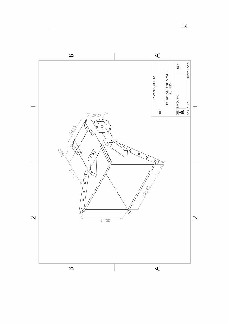
159
,44
5
130,14
74,
15
24,
55
84,
95
47,47 SIZE
TITLE
:
DW
G.
NO
.
ARE
V
SCA
LE: 1
:5HORN
AN
TEN
NA
V4.
1#
2 PR
INT
SHEE
T 1
OF
8
21
AB
AB
12
Univ
ersit
y of
Oslo
116
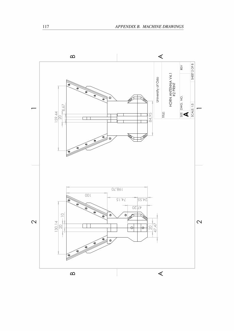
159
,44
84,
95 6
,67
20
130
,14
10
20
100 198,70
74,15 24,55
47,20
20
47,
47
SIZE
TITLE
:
DW
G.
NO
.
ARE
V
SCA
LE: 1
:5HORN
AN
TEN
NA
V4.
1#
2 PR
INT
SHEE
T 2
OF
8
21
AB
AB
12
Univ
ersit
y of
Oslo
117 APPENDIX B. MACHINE DRAWINGS
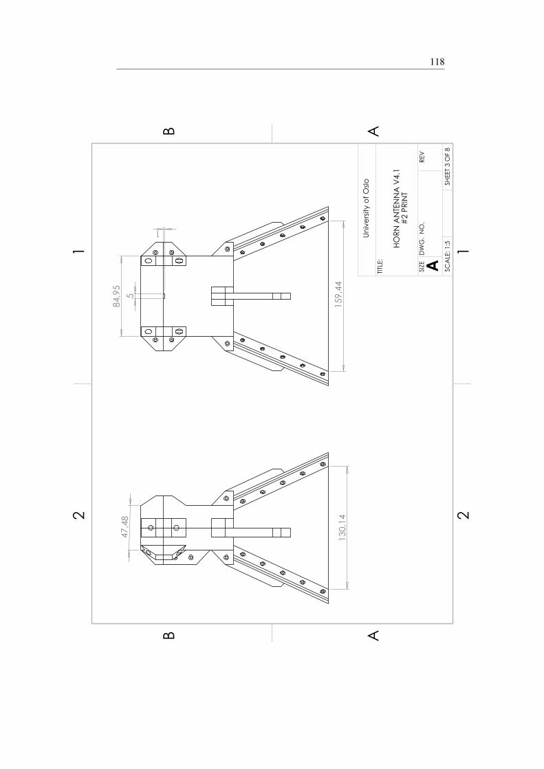
159
,44
84,
95
5
1
130
,14
47,
48
SIZE
TITLE
:
DW
G.
NO
.
ARE
V
SCA
LE: 1
:5HORN
AN
TEN
NA
V4.
1#
2 PR
INT
SHEE
T 3
OF
8
21
AB
AB
12
Univ
ersit
y of
Oslo
118
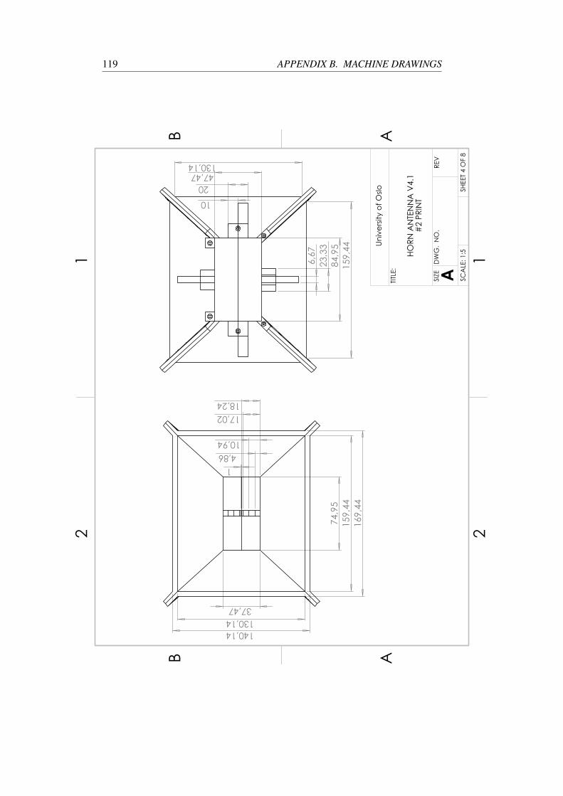
6,6
7 2
3,33
8
4,95
1
59,4
4
130,14 47,47
20 10
130,14
159
,44
74,
95
37,47
169
,44
140,14
18,24 17,02
10,94 4,86 1
SIZE
TITLE
:
DW
G.
NO
.
ARE
V
SCA
LE: 1
:5HORN
AN
TEN
NA
V4.
1#
2 PR
INT
SHEE
T 4
OF
8
21
AB
AB
12
Univ
ersit
y of
Oslo
119 APPENDIX B. MACHINE DRAWINGS

A A
47,
47
37,
47
27,
74
15,
59
3,4
3 1
1 23,75 17,49 18,74 21,74 11,99
74,15 24,55 98,70
130
,14
SEC
TION
A-A
SCA
LE 1
: 2
SIZE
TITLE
:
DW
G.
NO
.
ARE
V
SCA
LE: 1
:5HORN
AN
TEN
NA
V4.
1#
2 PR
INT
SHEE
T 5
OF
8
21
AB
AB
12
Univ
ersit
y of
Oslo
120
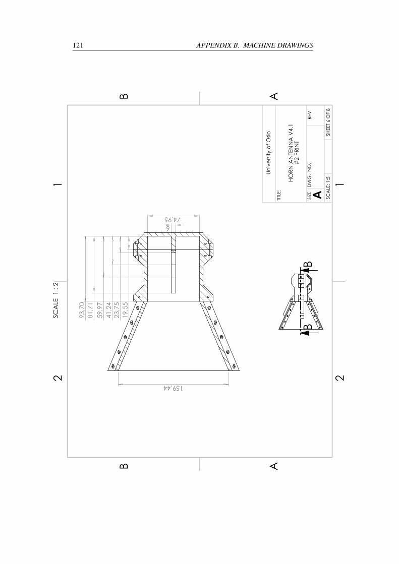
BB
159,44
93,
70
81,
71
19,
55
23,
75
41,
24
59,
97
6 74,95
SEC
TION
B-B
SCA
LE 1
: 2
SIZE
TITLE
:
DW
G.
NO
.
ARE
V
SCA
LE: 1
:5HORN
AN
TEN
NA
V4.
1#
2 PR
INT
SHEE
T 6
OF
8
21
AB
AB
12
Univ
ersit
y of
Oslo
121 APPENDIX B. MACHINE DRAWINGS

D D
11,
99
4,2
0 1
7,49
1
8,74
2
1,74
1,22 6,08 6,08 4,86
SEC
TION
D-D
SCA
LE 1
: 1.5
PCB
feed
Wa
vegu
ide
Ca
vity
Hor
n
SIZE
TITLE
:
DW
G.
NO
.
ARE
V
SCA
LE: 1
:5HORN
AN
TEN
NA
V4.
1#
2 PR
INT
SHEE
T 7
OF
8
21
AB
AB
12
Univ
ersit
y of
Oslo
122
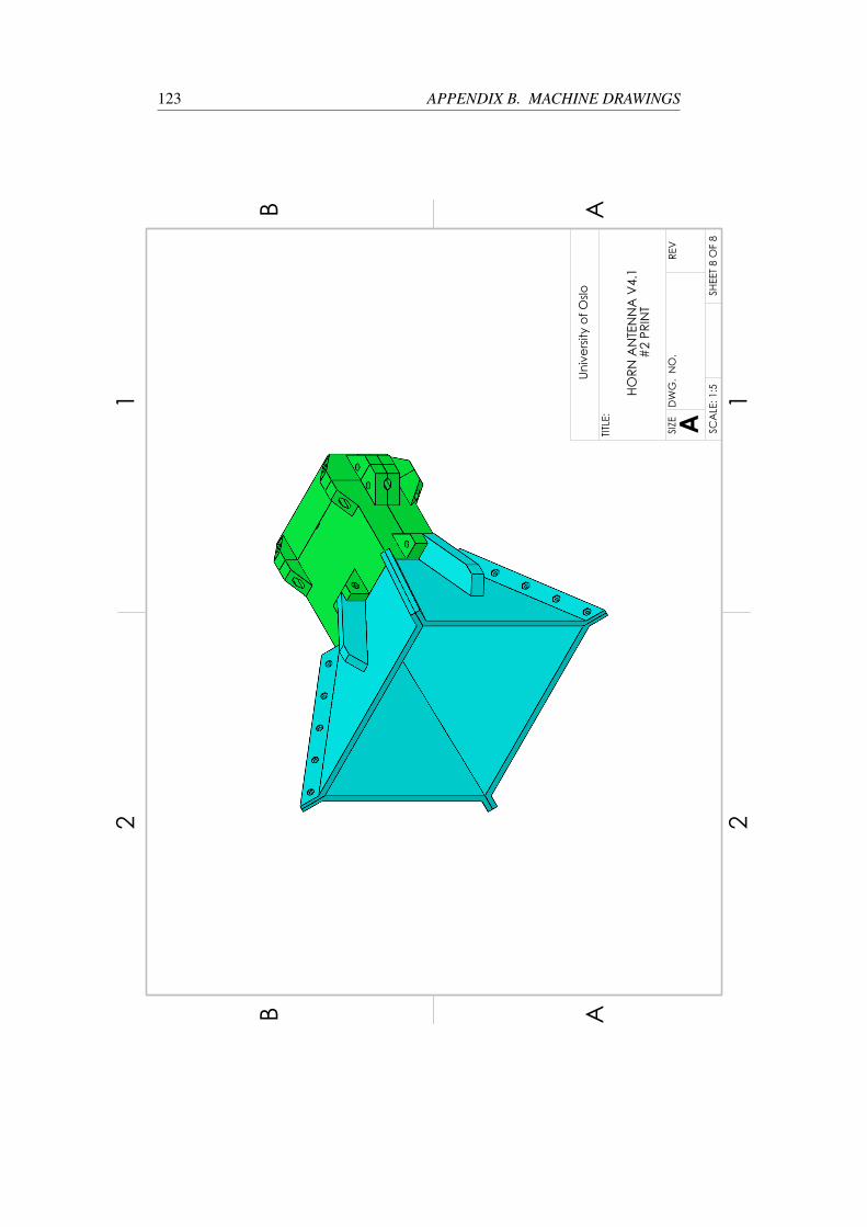
SIZE
TITLE
:
DW
G.
NO
.
ARE
V
SCA
LE: 1
:5HORN
AN
TEN
NA
V4.
1#
2 PR
INT
SHEE
T 8
OF
8
21
AB
AB
12
Univ
ersit
y of
Oslo
123 APPENDIX B. MACHINE DRAWINGS


