Embed Size (px)
Citation preview
APPLICATION OF ULTRA-WIDEBAND TECHNOLOGY TO RFID AND WIRELESS SENSORS
Ángel Ramos Félix
Dipòsit Legal: T 769-2015
ADVERTIMENT. L'accés als continguts d'aquesta tesi doctoral i la seva utilització ha de respectar els drets
de la persona autora. Pot ser utilitzada per a consulta o estudi personal, així com en activitats o materials d'investigació i docència en els termes establerts a l'art. 32 del Text Refós de la Llei de Propietat Intel·lectual (RDL 1/1996). Per altres utilitzacions es requereix l'autorització prèvia i expressa de la persona autora. En qualsevol cas, en la utilització dels seus continguts caldrà indicar de forma clara el nom i cognoms de la persona autora i el títol de la tesi doctoral. No s'autoritza la seva reproducció o altres formes d'explotació efectuades amb finalitats de lucre ni la seva comunicació pública des d'un lloc aliè al servei TDX. Tampoc s'autoritza la presentació del seu contingut en una finestra o marc aliè a TDX (framing). Aquesta reserva de drets afecta tant als continguts de la tesi com als seus resums i índexs. ADVERTENCIA. El acceso a los contenidos de esta tesis doctoral y su utilización debe respetar los
derechos de la persona autora. Puede ser utilizada para consulta o estudio personal, así como en actividades o materiales de investigación y docencia en los términos establecidos en el art. 32 del Texto Refundido de la Ley de Propiedad Intelectual (RDL 1/1996). Para otros usos se requiere la autorización previa y expresa de la persona autora. En cualquier caso, en la utilización de sus contenidos se deberá indicar de forma clara el nombre y apellidos de la persona autora y el título de la tesis doctoral. No se autoriza su reproducción u otras formas de explotación efectuadas con fines lucrativos ni su comunicación pública desde un sitio ajeno al servicio TDR. Tampoco se autoriza la presentación de su contenido en una ventana o marco ajeno a TDR (framing). Esta reserva de derechos afecta tanto al contenido de la tesis como a sus resúmenes e índices. WARNING. Access to the contents of this doctoral thesis and its use must respect the rights of the author. It
can be used for reference or private study, as well as research and learning activities or materials in the terms established by the 32nd article of the Spanish Consolidated Copyright Act (RDL 1/1996). Express and previous authorization of the author is required for any other uses. In any case, when using its content, full name of the author and title of the thesis must be clearly indicated. Reproduction or other forms of for profit use or public communication from outside TDX service is not allowed. Presentation of its content in a window or frame external to TDX (framing) is not authorized either. These rights affect both the content of the thesis and its abstracts and indexes.
Ángel Ramos Félix
APPLICATION OF ULTRA-WIDEBAND TECHNOLOGY TO RFID AND WIRELESS SENSORS
DOCTORAL THESIS
supervised by Dr. David Girbau Sala and Dr. Antonio Lázaro Guillén
Department
of Electronic, Electric and Automatic Control Engineering
Tarragona
2015
UNIVERSITAT ROVIRA I VIRGILI APPLICATION OF ULTRA-WIDEBAND TECHNOLOGY TO RFID AND WIRELESS SENSORS Ángel Ramos Félix DL: T 769-2015

UNIVERSITAT ROVIRA I VIRGILI APPLICATION OF ULTRA-WIDEBAND TECHNOLOGY TO RFID AND WIRELESS SENSORS Ángel Ramos Félix DL: T 769-2015

Escola Tècnica Superior d’Enginyeria Departament d’Enginyeria Electrònica, Elèctrica i Automàtica Avda. Dels Països Catalans, 26 Campus Sescelades 43007 Tarragona Tel. (+0034) 977 55 9610 Fax (+0034) 977 55 9605 We STATE that the present study, entitled “Application of Ultra-Wideband Technology to RFID and Wireless Sensors”, presented by Ángel Ramos Félix for the award of the degree of Doctor, has been carried out under our supervision at the Department of Electronic, Electric and Automatic Control Engineering of this university, and that it fulfills all the requirements to be eligible for the International Doctorate Award.
Tarragona, 28th January 2015
Doctoral Thesis Supervisors
David Girbau Sala Antonio Lázaro Guillén
UNIVERSITAT ROVIRA I VIRGILI APPLICATION OF ULTRA-WIDEBAND TECHNOLOGY TO RFID AND WIRELESS SENSORS Ángel Ramos Félix DL: T 769-2015

UNIVERSITAT ROVIRA I VIRGILI APPLICATION OF ULTRA-WIDEBAND TECHNOLOGY TO RFID AND WIRELESS SENSORS Ángel Ramos Félix DL: T 769-2015
Acknowledgement A lot of people has been, in one way or another, involved in the realization of this Thesis. I would like to thank them all: First of all, my supervisors Dr. Antonio Lázaro and Dr. David Girbau. They have been great advisors even since I started taking their degree classes back in 2008. I am grateful that they offered me the opportunity to work in something I like, with the added luck of being so close to my home town. I have learned a lot from them through all these years, and I hope that I can work with them again in the future. Dr. Ramón Villarino, who has also been very helpful with a lot of laboratory-related issues. Pierrick Clément and Dr. Eduard Llobet, from the DEEEA at URV, and Dr. Apostolos Georgiadis and Dr. Ana Collado, from the CTTC, who I had the pleasure to collaborate with during my Thesis. The people at the LCIS in Valence, France. It has been very fruitful to stay several months working with Prof. Smail Tedjini and Dr. Etienne Perret. I would also like to mention the PhD students Gianfranco and Marco: the talks with them have been very entertaining. The people that have been with me every day at the office. I would like to specially mention the people I have been with most of the time: both Javier Lorenzo and Javier Corea, Oana and Bogdan. All the administrative and technical personnel of the DEEEA (and the URV in general), who have always kindly helped me with paperwork, congress registrations, flights and hotel bookings or ordering components. Last but not least, my family and friends. My parents Ángel and Inés, and my brother, Javier, have been and will be always there.
UNIVERSITAT ROVIRA I VIRGILI APPLICATION OF ULTRA-WIDEBAND TECHNOLOGY TO RFID AND WIRELESS SENSORS Ángel Ramos Félix DL: T 769-2015
This work has been funded by:
- The Spanish Government Projects TEC2008-06758-C02-02 and TEC2011-28357-C02-01
- Universitat Rovira i Virgili grant 2011BRDI-06-08
- AGAUR Grant FI-DGR 2012
UNIVERSITAT ROVIRA I VIRGILI APPLICATION OF ULTRA-WIDEBAND TECHNOLOGY TO RFID AND WIRELESS SENSORS Ángel Ramos Félix DL: T 769-2015
List of Publications Indexed Journals
[J.1] A. Ramos, A. Lazaro, D. Girbau, and R. Villarino, “Time-domain measurement of time-
coded UWB chipless RFID tags,” Progress In Electromagnetics Research, Vol. 116, pp. 313-331, 2011.
[J.2] A. Lazaro, A. Ramos, D. Girbau, and R. Villarino, “Chipless UWB Tag Detection using
Continuous Wavelet Transform,” IEEE Antennas and Wireless Propagation Letters, Vol. 10, pp. 520-523, 2011.
[J.3] D. Girbau, A. Ramos, A. Lazaro, and R. Villarino, “Passive Wireless Temperature
Sensor Based on Time-Coded UWB Chipless RFID Tags,” IEEE Transactions on Microwave Theory and Techniques, Vol. 60, No. 11, pp. 3623-3632, 2012.
[J.4] A. Lazaro, A. Ramos, R. Villarino, and D. Girbau, “Active UWB Reflector for RFID and
Wireless Sensor Networks,” IEEE Transactions on Antennas and Propagation, Vol. 61, No. 9, pp. 4767-4774, 2013.
[J.5] A. Ramos, A. Lazaro, and D. Girbau, “Semi-Passive Time-Domain UWB RFID System,”
IEEE Transactions on Microwave Theory and Techniques, Vol. 61, No. 4, pp. 1700-1708, 2013.
[J.6] A. Lazaro, A. Ramos, R. Villarino, and D. Girbau, “Time-domain UWB RFID tag based
on Reflection Amplifier,” IEEE Antennas and Wireless Propagation Letters, Vol. 12, pp. 520-523, 2013.
[J.7] A. Lazaro, A. Ramos, D. Girbau, and R. Villarino, “A Novel UWB RFID tag using Active
Frequency Selective Surface,” IEEE Transactions on Antennas and Propagation, Vol. 61, No. 3, pp. 1155-1165, 2013.
[J.8] P. Clement, A. Ramos, A. Lazaro, L. Molina-Luna, C. Bittencourt, D. Girbau, and
E. Llobet, “Oxygen plasma treated carbon nanotubes for the wireless monitoring of nitrogen dioxide levels,” Sensors and Actuators B: Chemical, Vol. 208, pp. 444-449, 2015.
[J.9] A. Ramos, P. Clement, A. Lazaro, E. Llobet, and D. Girbau, “Nitrogen Dioxide Wireless
Sensor based on Carbon Nanotubes and UWB RFID Technology,” IEEE Antennas and Wireless Propagation Letters, pp. – (Early Access), 2015.
[J.10] A. Ramos, A. Lazaro, D. Girbau, A. Collado, and A. Georgiadis, “Solar-Powered Wireless Temperature Sensor Based on UWB RFID with Self-Calibration,” IEEE Sensors Journal, 2015. Accepted (Jan. 2015).
International Conferences
[C.1] A. Ramos, D. Girbau, and A. Lazaro, “Influence of materials in time-coded chipless
RFID tags characterized using a low-cost reader,” 42nd
European Microwave Conference, pp. 526-529, Amsterdam (The Netherlands), Nov. 2012.
[C.2] A. Ramos, D. Girbau, A. Lazaro, and S. Rima, “IR-UWB Radar System and Tag Design for Time-coded Chipless RFID,” 6
th European Conference on Antennas and
Propagation, pp. 2491-2494, Prague (Czech Republic), Mar. 2012.
UNIVERSITAT ROVIRA I VIRGILI APPLICATION OF ULTRA-WIDEBAND TECHNOLOGY TO RFID AND WIRELESS SENSORS Ángel Ramos Félix DL: T 769-2015
[C.3] D. Girbau, A. Lazaro, and A. Ramos, “Time-coded chipless RFID tags: Design, characterization and application,” IEEE International Conference on RFID Technology and Applications (RFID-TA 2012), pp. 12-17, Nice (France), Nov. 2012.
[C.4] A. Ramos, D. Girbau, A. Lazaro, and R. Villarino, “Time-coded chipless RFID temperature sensor with self-calibration based on Vivaldi antenna,” IEEE International Microwave Symposium (IMS 2013), pp. 1-4, Seattle (United States of America), Jun. 2013.
[C.5] A. Lazaro, R. Villarino, A. Ramos, and D. Girbau, “Active frequency selective surface for time-domain UWB RFID applications,” 43
rd European Microwave Conference, pp. 136-
139, Nuremberg (Germany), Oct. 2013.
[C.6] A. Ramos, D. Girbau, A. Lazaro, and R. Villarino, “Permittivity sensor using chipless time-coded UWB RFID,” 2014 XXXIth URSI General Assembly and Scientific Symposium (URSI GASS 2014), pp. 1-4, Beijing (China), Aug. 2014.
[C.7] A. Ramos, A. Lazaro, R. Villarino, and D. Girbau, “Time-domain UWB RFID tags for smart floor applications,” IEEE International Conference on RFID Technology and Applications (RFID-TA 2014), pp. 165-169, Tampere (Finland), Sep. 2014.
[C.8] A. Ramos, A. Lazaro, and D. Girbau, “Multi-sensor UWB time-coded RFID tags for smart cities applications,” 44
th European Microwave Conference, pp. 259-262, Rome
(Italy), Oct. 2014. [C.9] A. Ramos, A. Lazaro, R. Villarino, and D. Girbau, “Sensing of thermal thresholds using
UWB RFID passive tags,” IEEE Sensors 2014, pp. 1503-1506, Valencia (Spain), Nov. 2014.
UNIVERSITAT ROVIRA I VIRGILI APPLICATION OF ULTRA-WIDEBAND TECHNOLOGY TO RFID AND WIRELESS SENSORS Ángel Ramos Félix DL: T 769-2015
Index 1. Introduction 1
1.1. RFID: State of the art 1 1.1.1. Introduction to RFID 1 1.1.2. Chipless RFID 4
1.2. Extending RFID capabilities: from identification to sensing 7 1.2.1. Existing technologies for wireless sensors 8 1.2.2. RFID-enabled wireless sensors 9
1.3. Ultra-Wideband technology for RFID applications 10 1.3.1. Introduction to UWB technology 10 1.3.2. UWB-based RFID 11
1.4. Objectives of this Doctoral Thesis 13 1.5. Organization of this document 13 1.6. Bibliography 14
2. Chipless Time-Coded UWB RFID 19
2.1. Introduction 19 2.2. Theory 19 2.3. Reader design 25
2.3.1. Frequency-step approach 25 2.3.2. Impulse-based approach 25 2.3.3. Comparison and conclusions 27
2.4. Signal processing techniques 29 2.4.1. Time-windowing and background subtraction 29 2.4.2. Continuous Wavelet Transform 30
2.5. Design of chipless time-coded UWB RFID tags 34 2.5.1. Design of UWB antennas 34 2.5.2. Integrating delay lines with UWB antennas 38 2.5.3. Circularly polarized UWB RFID tags 42
2.6. Characterization of chipless time-coded UWB tags 44 2.6.1. Time-domain response: distance and resolution 44 2.6.2. Angular behaviour 49 2.6.3. Influence of materials 50 2.6.4. Polarization 56 2.6.5. Flexible substrates: bending 57
2.7. Conclusions 61 2.8. Bibliography 62
3. Chipless Time-Coded UWB Wireless Sensors 67
3.1. Introduction: cost, reliability and hazardous environments 67 3.2. Amplitude-based chipless time-coded UWB sensors 68
3.2.1. Principle of operation 68 3.2.2. Temperature sensor based on chipless time-coded UWB
tags 69
3.2.2.1. Sensor design and characterization 70 3.2.2.2. Results 71
3.2.3. Temperature threshold detectors based on chipless time-coded UWB tags
78
3.2.3.1. Threshold detector using shape memory alloys 79
UNIVERSITAT ROVIRA I VIRGILI APPLICATION OF ULTRA-WIDEBAND TECHNOLOGY TO RFID AND WIRELESS SENSORS Ángel Ramos Félix DL: T 769-2015
3.2.3.2. Threshold detector using a thermal switch 81 3.2.3.3. Detection techniques for threshold detectors 84
3.2.4. Self-calibration and reliability 86 3.3. Delay-based chipless time-coded sensors 92
3.3.1. Principle of operation 92 3.3.2. Permittivity sensor based on chipless time-coded UWB
tags 95
3.3.2.1. Sensor design 95 3.3.2.2. Concrete composition detection 100 3.3.2.3. Results 101
3.4. Conclusions 105 3.5. Bibliography 106
4. Semi-Passive Time-Coded UWB RFID 109
4.1. Introduction 109 4.2. Wake-up system 110
4.2.1. Overview 110 4.2.2. Schottky diode-based detector 111 4.2.3. Reader. Modulation schemes 113 4.2.4. Interferences and coexistence with other systems 114
4.3. Microcontroller-based semi-passive UWB RFID system 115 4.3.1. Introduction: chip-based UWB RFID tags 115 4.3.2. Microcontroller: tag core logic 117 4.3.3. UWB backscatterer design and evaluation 118 4.3.4. Differential coding and detection techniques 121 4.3.5. Communication protocol 123 4.3.6. System scalability, applications and sensor integration 124 4.3.7. Results 125
4.4. Analog semi-passive UWB RFID system 129 4.4.1. Introduction 129 4.4.2. Switch-based UWB Backscatterer 131 4.4.3. PIN diode-based UWB Backscatterer 134 4.4.4. Detector circuit design 136
4.5. Discussion, comparison between systems and conclusions 138 4.6. Bibliography 139
5. Semi-Passive Time-Coded UWB Wireless Sensors 143
5.1. Introduction 143 5.2. Solar-powered temperature sensor based on analog semi-
passive UWB RFID 143
5.2.1. Introduction 143 5.2.2. Sensor design and calibration 144 5.2.3. Solar-cell Integration. Power requirements 146 5.2.4. Results and error study 148
5.3. Nitrogen dioxide gas sensor based on analog semi-passive UWB RFID
153
5.3.1. Introduction 153 5.3.2. Carbon nanotube-based Nitrogen dioxide sensor 154 5.3.3. Wireless sensor design and calibration 157 5.3.4. Results 158
UNIVERSITAT ROVIRA I VIRGILI APPLICATION OF ULTRA-WIDEBAND TECHNOLOGY TO RFID AND WIRELESS SENSORS Ángel Ramos Félix DL: T 769-2015
5.4. Sensor integration in microcontroller-based semi-passive UWB RFID
162
5.4.1. Multi-sensor tag 162 5.4.2. Nitrogen dioxide gas sensor 164
5.5. Comparison between chipless and semi-passive approaches. Conclusions
166
5.6. Bibliography 168
6. Smart Floor Applications using Time-Coded UWB RFID and Ground Penetrating Radar
171
6.1. Introduction 171 6.2. Smart floor design. Alternatives 171 6.3. Results 173
6.3.1. Smart floor based on passive reflectors 173 6.3.2. Smart floor based on chipless time-coded UWB RFID tags 176 6.3.3. Smart floor based on semi-passive time-coded UWB RFID
tags 179
6.4. Conclusion 179 6.5. Bibliography 180
7. Active Time-Coded UWB RFID 181 7.1. Introduction 181 7.2. Active UWB RFID system based on cross-polarization amplifier 181
7.2.1. Introduction 182 7.2.2. Cross-polarization amplifier design 182 7.2.3. UWB and UHF link budget 187 7.2.4. Results 190
7.3. Active UWB RFID system based on reflection amplifier 193 7.3.1. Introduction 193 7.3.2. Reflection amplifier design 194 7.3.3. System link budget 197 7.3.4. Results 198
7.4. Discussion and comparison between systems 199 7.5. Bibliography 201
8. Chipless Frequency-Coded RFID Tag Detection using Short-
Time Fourier Transform 203
8.1. Introduction 203 8.2. Theory 205
8.2.1. Depolarizing frequency-coded chipless RFID 205 8.2.2. Short-time Fourier transform 206
8.3. Quality factor of REP tags 208 8.4. Measurements 211
8.4.1. Measurement setup and tags 211 8.4.2. Using the STFT to detect depolarizing tags 211
8.5. Conclusion 213 8.6. Bibliography 215
9. General Conclusions 217
UNIVERSITAT ROVIRA I VIRGILI APPLICATION OF ULTRA-WIDEBAND TECHNOLOGY TO RFID AND WIRELESS SENSORS Ángel Ramos Félix DL: T 769-2015
UNIVERSITAT ROVIRA I VIRGILI APPLICATION OF ULTRA-WIDEBAND TECHNOLOGY TO RFID AND WIRELESS SENSORS Ángel Ramos Félix DL: T 769-2015

1. Introduction
1
1. Introduction Automatic identification of goods is widely used in industry, logistics, medicine and other fields. The aim is to obtain the identification information (ID) of a good in transit. Giant electronic commerce platforms such as Amazon, Alibaba or eBay are becoming the main choice for buyers worldwide [1.1]. Instead of buying from a small retailer, final customers are directly in contact with a wholesaler or distributor. In this context, an accurate tracking of each good to its final customer is a major concern in a massive growing logistics market. Also, an efficient, automatic organization of the stock in large warehouses (both sellers‟ and logistics companies) is crucial to reduce costs and delivery times. Nowadays, barcode (see Figure 1.1) is the most used automatic identification solution [1.2]. It consists of a reader which optically reads a tag. The tag is created by printing black stripes on a white background. Depending on the number of stripes, width and separation, a unique identification (ID) is generated. In order to code more information in a smaller space, variations such as QR Codes [1.3] have arisen recently. The cost of each barcode tag is extremely cheap because it only requires paper and ink. In addition, barcode readers are also cheap, and even low-cost compact mobile phone cameras can provide high resolution images to read barcodes [1.4]. However, it requires a direct line-of-sight between the reader and the tag. A specific positioning of the object is required in order to orientate the barcode towards the reader, and normally only one tag can be read at a time. Also, the barcode storage capacity is limited, and they cannot be reprogrammed. Another common problem with barcodes is misreadings due to a low resolution printing of the tag, or ink wearing away in harsh environments.
Figure 1.1. Photograph of a barcode system
1.1. RFID: State of the art 1.1.1. Introduction to RFID In order to overcome barcode limitations, Radio Frequency IDentification (RFID) technologies have been developed in the last years [1.5]. RFID systems are used to remotely retreive data from target objects (tags) without the need to have physical contact or line-of-sight, by using magnetic or electromagnetic (EM) waves. With some RFID systems it is also possible to measure several tags at the same time, and rewrite the tag information.
UNIVERSITAT ROVIRA I VIRGILI APPLICATION OF ULTRA-WIDEBAND TECHNOLOGY TO RFID AND WIRELESS SENSORS Ángel Ramos Félix DL: T 769-2015
Application of Ultra-Wideband Technology to RFID and Wireless Sensors
2
Figure 1.2 shows a basic scheme of an RFID system. There are two main families: near-field RFID (Figure 1.2a) and far-field RFID (Figure 1.2b) [1.6]. Near-field RFID is based on the Faraday‟s principle of magnetic induction (magnetic coupling). Both the reader and the tag have coils. The reader powers up the tag‟s transponder chip, which can be rewritten. Near-field RFID based on this inductive communication is used for small distances, typically below λ/(2π) where λ is the wavelength [1.6]. ISO 15693 and 14443 standards set frequencies below 14 MHz, which results in a range of a few centimeters. Near-field RFID is widely used for cards and access control, but not for goods management due to its limited range. Far-field RFID uses electromagnetic waves propagated through antennas both in the reader and the tag. A reader can be monostatic if it only has an antenna which acts for transmission (Tx) and reception (Rx). On the contrary, if the reader has separate Tx and Rx antennas, it is bistatic. The reader sends an EM wave which is captured by the tag‟s antenna at several meters of distance. There are several standards for far-field RFID, with the EPC Gen2 standard, at the UHF (868 MHz in Europe or 915 MHz in the United States) band, being the most used.
Object to be
identifiedTag
Reader
Application
Transponder
Chip
Coil
Coil
Few cm
-a-
Tag
Reader
Application
Antenna(s)
Transponder
or Reflector
Antenna(s)
Object to be
identified
Up to several
meters -b-
Figure 1.2. Scheme of an RFID system, (a) near-field and (b) far-field
Even though barcode is still the de facto standard, RFID is one of the fastest growing sectors of the radio technology. As of 2014, nearly every commercially available smartphone integrates near-field RFID with Near Field Communication Forum‟s (NFC) standards [1.7]. Wal-Mart and Tesco, some of the largest retailers in the United States and the United Kingdom respectively, are adopting RFID [1.6]. Furthermore, wireless identification has developed into an interdisciplinary field. Radio Frequency (RF) technology, semiconductor technology, data protection and crypthography, telecommunications and related areas are joined to develop cheap, secure, reliable, long-range and self-powered RFID tags. Far-field RFID systems can be classified depending on how the tags get the
UNIVERSITAT ROVIRA I VIRGILI APPLICATION OF ULTRA-WIDEBAND TECHNOLOGY TO RFID AND WIRELESS SENSORS Ángel Ramos Félix DL: T 769-2015
1. Introduction
3
necessary energy to respond to the readers. Active tags are the most expensive ones, since they need their own power supply (i.e., batteries) not only to power their own chip but also to generate the radio signal with the response to the reader. Semi-passive tags are less expensive than active ones, since they need batteries, but only to power their own logic circuitry, not a transmitter. The response is achieved by changing the reflected signal from the reader, in a process called backscattering. This means that the batteries can be smaller and have longer life times (usually years). Finally, passive tags are the cheapest ones and have the largest commercial potential for large-scale spreading [1.8-1.9]. Passive tags use the reader‟s RF signal to harvest the necessary power for themselves [1.8]. Specifically, passive UHF EPC tags are the type of RFID tags most widely used for large-scale applications. Depending on the region, there are different frequency bands and maximum allowed powers allocated for RFID applications [1.10]. In Europe, the most used band is at 865.6 – 867.6 MHz, with a maximum transmitted power of 2 W of Effective Radiated Power (ERP), or, equivalently, 3.28 W of Effective Isotropic Radiated Power (EIRP). Similarly, in the United States of America the allowed RFID band is at 902 – 928 MHz, with a maximum transmitted power of 4 W EIRP, or, equivalently, 2.44 W of ERP. As it can be observed, American regulations permit more transmitted power than European ones, allowing for longer read ranges. Most manufacturers provide UHF RFID tags and readers compatible with both European and American bands. Figure 1.3 shows an example of a typical commercial UHF EPC Gen2 reader and tag from Alien Technology. These type of tags have a sensitivity of about -20 dBm [1.11-1.12], and read-ranges between 6 and 10 m depending on the region [1.13]. Some recent research has increased the read range to about 25 m by assisting the tag with a battery (Battery-Assisted Passive tags) [1.14].
-a-
IC (Chip)
-b-
Figure 1.3. (a) Alien ALR-9900 UHF EPC Gen2 RFID reader. (b) Alien ALN9740 UHF RFID tag
There have been also recent developments in Millimeter Wave bands. Millimeter Wave IDentification (MMID) has been presented in [1.15] as a concept of RFID operating at 60 GHz. MMID is not a replacement of RFID, since its read range is much shorter (a few centimeters). MMID, however, permits high data-rate communications (even gigabit). Also, directive antennas at millimeter wave frequencies are very small compared to UHF, permitting the possibility of selecting a tag by pointing towards it. The use of non linear devices for RFID tags has also been studied recently. Tags based on the
UNIVERSITAT ROVIRA I VIRGILI APPLICATION OF ULTRA-WIDEBAND TECHNOLOGY TO RFID AND WIRELESS SENSORS Ángel Ramos Félix DL: T 769-2015

Application of Ultra-Wideband Technology to RFID and Wireless Sensors
4
intermodulation distortion (IMD) of devices have been presented in [1.16] using a diode for localization applications, and in [1.17] using microelectromechanical systems (MEMS). 1.1.2. Chipless RFID A specific type of passive RFID tags are chipless tags. In these tags, instead of storing the ID in a digital IC, it is stored in physical permanent modifications when the tag is fabricated. These modifications change from one tag to another. A notable reduction in costs for passive UHF tags has been achieved recently [1.8] due to the popularization in using RFID technology. However, each UHF tag price is fixed by the chip and by the process of connecting it to the tag antenna. In consequence, using chip-based tags is non-viable for identifying large volumes of paper or plastic documents such as banknotes, postage stamps, tickets or envelopes, since the price of the tag is larger than the document itself [1.9]. UHF RFID technology, also, presents some weaknesses. UHF frequency-band allocation depends on the region, as well as the readers‟ output-signal power, which affects directly to the read range (the more power allowed, the longer the read distance is). UHF tags are affected by multipath propagation [1.18], interference between readers [1.19], and frequency detuning due to different materials used as the tag physical support [1.20]; factors which can lead to smaller read ranges. Also, it is necessary to consider special tags, used when attached to metal surfaces, that increase the total price.
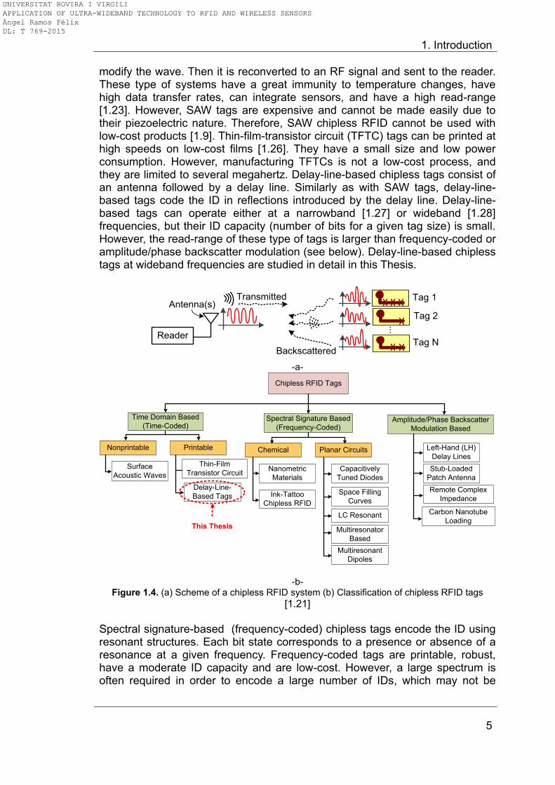
Chipless tags can be a promising low-cost alternative for RFID systems, since they do not need an IC to work [1.21-1.22]. In chipless tags, the ID is stored in physical permanent modifications in a scattering antenna. The modifications are unique for each tag, and change its RF backscattered response, or signature. Figure 1.4a shows a scheme of a chipless RFID system. It is important to note that chipless tags cannot change their information once they have been fabricated, since their physical characteristics are permanent. However, chipless RFID can provide a low-cost alternative, which could increase the capabilities of barcode. Since there does not exist a standard for chipless RFID, there are several types of approaches under active research to achieve chipless RFID tags. Figure 1.4b shows a classification of chipless RFID tags given in [1.21]. One drawback with chipless RFID tags compared with chip-based tags is the small number of possible IDs [1.21-1.22]. However, this drawback is not very important if the chipless tag integrates additional capabilities beyond identification such as sensing.
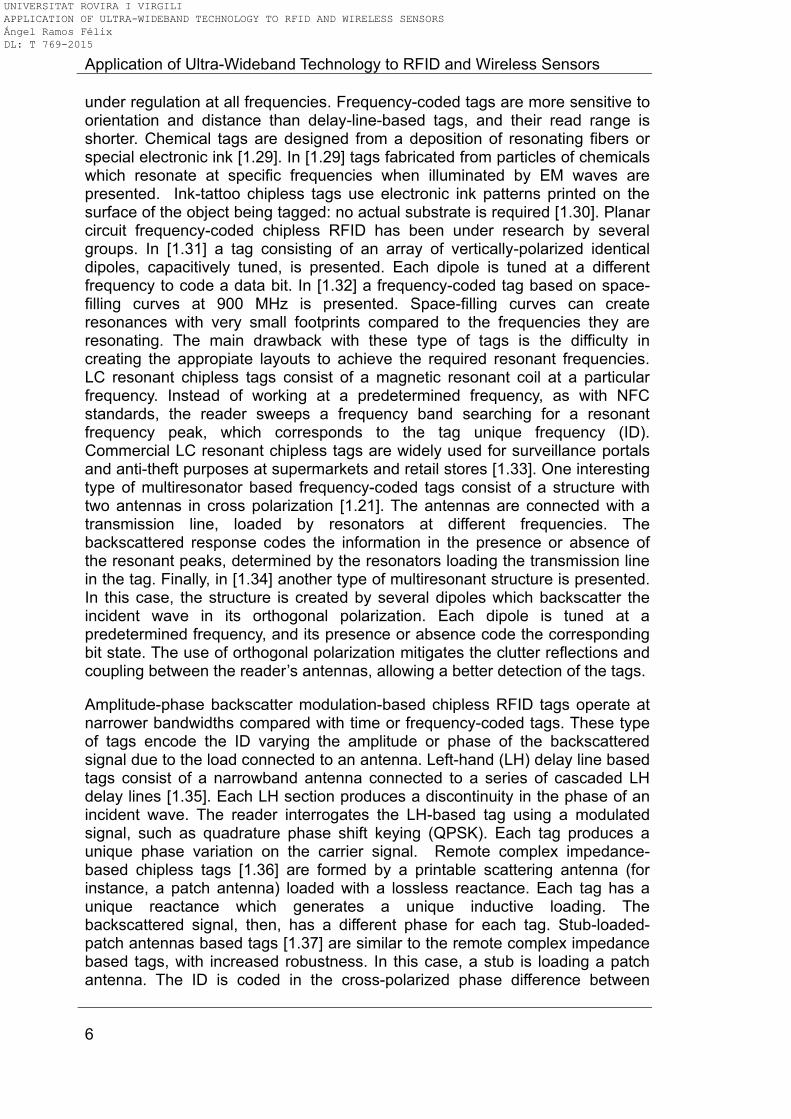
Time-domain based (time-coded) tags encode the ID in the time delay of a reflected peak. Surface Acoustic Wave (SAW) technology offers a nonprintable alternative for chipless RFID [1.23-1.25]. SAW RFID is usually based on passive RFID systems, where the signal from the reader is converted into an acoustical wave. A scheme of a SAW tag is shown in Figure 1.5. The acoustical wave incides a substrate, where multiple reflections in different time instants
UNIVERSITAT ROVIRA I VIRGILI APPLICATION OF ULTRA-WIDEBAND TECHNOLOGY TO RFID AND WIRELESS SENSORS Ángel Ramos Félix DL: T 769-2015
1. Introduction
5
modify the wave. Then it is reconverted to an RF signal and sent to the reader. These type of systems have a great immunity to temperature changes, have high data transfer rates, can integrate sensors, and have a high read-range [1.23]. However, SAW tags are expensive and cannot be made easily due to their piezoelectric nature. Therefore, SAW chipless RFID cannot be used with low-cost products [1.9]. Thin-film-transistor circuit (TFTC) tags can be printed at high speeds on low-cost films [1.26]. They have a small size and low power consumption. However, manufacturing TFTCs is not a low-cost process, and they are limited to several megahertz. Delay-line-based chipless tags consist of an antenna followed by a delay line. Similarly as with SAW tags, delay-line-based tags code the ID in reflections introduced by the delay line. Delay-line-based tags can operate either at a narrowband [1.27] or wideband [1.28] frequencies, but their ID capacity (number of bits for a given tag size) is small. However, the read-range of these type of tags is larger than frequency-coded or amplitude/phase backscatter modulation (see below). Delay-line-based chipless tags at wideband frequencies are studied in detail in this Thesis.
Reader
Antenna(s)Tag 1
Tag 2
...
Tag N
Transmitted
Backscattered
-a-
Chipless RFID Tags
Time Domain Based
(Time-Coded)
Nonprintable
Surface
Acoustic Waves
Printable
Thin-Film
Transistor Circuit
Delay-Line-
Based Tags
Chemical
Nanometric
Materials
Spectral Signature Based
(Frequency-Coded)
Ink-Tattoo
Chipless RFID
Planar Circuits
Capacitively
Tuned Diodes
Space Filling
Curves
LC Resonant
Multiresonator
Based
Multiresonant
Dipoles
Amplitude/Phase Backscatter
Modulation Based
Left-Hand (LH)
Delay Lines
Stub-Loaded
Patch Antenna
Remote Complex
Impedance
Carbon Nanotube
LoadingThis Thesis
-b-
Figure 1.4. (a) Scheme of a chipless RFID system (b) Classification of chipless RFID tags
[1.21]
Spectral signature-based (frequency-coded) chipless tags encode the ID using resonant structures. Each bit state corresponds to a presence or absence of a resonance at a given frequency. Frequency-coded tags are printable, robust, have a moderate ID capacity and are low-cost. However, a large spectrum is often required in order to encode a large number of IDs, which may not be
UNIVERSITAT ROVIRA I VIRGILI APPLICATION OF ULTRA-WIDEBAND TECHNOLOGY TO RFID AND WIRELESS SENSORS Ángel Ramos Félix DL: T 769-2015
Application of Ultra-Wideband Technology to RFID and Wireless Sensors
6
under regulation at all frequencies. Frequency-coded tags are more sensitive to orientation and distance than delay-line-based tags, and their read range is shorter. Chemical tags are designed from a deposition of resonating fibers or special electronic ink [1.29]. In [1.29] tags fabricated from particles of chemicals which resonate at specific frequencies when illuminated by EM waves are presented. Ink-tattoo chipless tags use electronic ink patterns printed on the surface of the object being tagged: no actual substrate is required [1.30]. Planar circuit frequency-coded chipless RFID has been under research by several groups. In [1.31] a tag consisting of an array of vertically-polarized identical dipoles, capacitively tuned, is presented. Each dipole is tuned at a different frequency to code a data bit. In [1.32] a frequency-coded tag based on space-filling curves at 900 MHz is presented. Space-filling curves can create resonances with very small footprints compared to the frequencies they are resonating. The main drawback with these type of tags is the difficulty in creating the appropiate layouts to achieve the required resonant frequencies. LC resonant chipless tags consist of a magnetic resonant coil at a particular frequency. Instead of working at a predetermined frequency, as with NFC standards, the reader sweeps a frequency band searching for a resonant frequency peak, which corresponds to the tag unique frequency (ID). Commercial LC resonant chipless tags are widely used for surveillance portals and anti-theft purposes at supermarkets and retail stores [1.33]. One interesting type of multiresonator based frequency-coded tags consist of a structure with two antennas in cross polarization [1.21]. The antennas are connected with a transmission line, loaded by resonators at different frequencies. The backscattered response codes the information in the presence or absence of the resonant peaks, determined by the resonators loading the transmission line in the tag. Finally, in [1.34] another type of multiresonant structure is presented. In this case, the structure is created by several dipoles which backscatter the incident wave in its orthogonal polarization. Each dipole is tuned at a predetermined frequency, and its presence or absence code the corresponding bit state. The use of orthogonal polarization mitigates the clutter reflections and coupling between the reader‟s antennas, allowing a better detection of the tags.
Amplitude-phase backscatter modulation-based chipless RFID tags operate at narrower bandwidths compared with time or frequency-coded tags. These type of tags encode the ID varying the amplitude or phase of the backscattered signal due to the load connected to an antenna. Left-hand (LH) delay line based tags consist of a narrowband antenna connected to a series of cascaded LH delay lines [1.35]. Each LH section produces a discontinuity in the phase of an incident wave. The reader interrogates the LH-based tag using a modulated signal, such as quadrature phase shift keying (QPSK). Each tag produces a unique phase variation on the carrier signal. Remote complex impedance-based chipless tags [1.36] are formed by a printable scattering antenna (for instance, a patch antenna) loaded with a lossless reactance. Each tag has a unique reactance which generates a unique inductive loading. The backscattered signal, then, has a different phase for each tag. Stub-loaded-patch antennas based tags [1.37] are similar to the remote complex impedance based tags, with increased robustness. In this case, a stub is loading a patch antenna. The ID is coded in the cross-polarized phase difference between
UNIVERSITAT ROVIRA I VIRGILI APPLICATION OF ULTRA-WIDEBAND TECHNOLOGY TO RFID AND WIRELESS SENSORS Ángel Ramos Félix DL: T 769-2015
1. Introduction
7
electric (E) and magnetic (H) planes. Finally, carbon nanotube-loaded chipless tags consist of RFID antennas loaded by carbon nanotubes (CNTs), which modify the scattering signature depending on their state. In [1.38] a conformal UHF RFID antenna is loaded with single-walled CNTs to realize a chipless RFID gas sensor. In summary, chipless RFID is a field of interest in RFID. There does not exist a common standard as in passive UHF RFID. Therefore, chipless RFID is still under active research. There are advantages and disadvantages between each approach, and the final application will decide which approach is chosen. Most of the published work on chipless RFID relies on using high-cost laboratory instruments as readers to demonstrate the feasibility of the proposed tags. However, there is an increasing interest in developing custom readers [1.22], which would reduce costs and enable the adoption of chipless RFID for specific market niches.
Reader
Antenna(s)
Transmitted
Backscattered
Antenna Reflectors
Transducer
Figure 1.5. Scheme of a SAW tag
1.2. Extending RFID capabilities: from identification to sensing There have been a large amount of advances in the miniaturization and cost reduction of advanced sensors [1.39]. A large number of applications can benefit from the information about their environment these sensors can obtain. Smart homes [1.40] or smart cities [1.41] are concepts which have flourished recently. In both cases, one of the main ideas is to crow an area (either houses or cities) with small, self-autonomous and low-cost sensors. These sensors are connected creating so-called sensor networks [1.39]. For large-scale applications, wiring each sensor is not viable. Also, some sensors can be placed in areas difficult to access. Therefore, wireless radio technologies which enable the sensors to be read remotely, creating a sensor node, are desired. The association of these wirelessly readable sensor nodes is called a wireless sensor network (WSN). Apart from smart homes or smart cities, WSNs also have a great potential in a large number of applications such as [1.39]: military target tracking and surveillance, natural disaster relief, biomedical health monitoring, hazardous environment exploration and seismic sensing. Low-power communication technologies are required to achieve years of lifetime for wireless sensors. Careful design on these technologies, based on small data rates (for small amounts of information, only sensor readings) has to be taken into account.
UNIVERSITAT ROVIRA I VIRGILI APPLICATION OF ULTRA-WIDEBAND TECHNOLOGY TO RFID AND WIRELESS SENSORS Ángel Ramos Félix DL: T 769-2015
Application of Ultra-Wideband Technology to RFID and Wireless Sensors
8
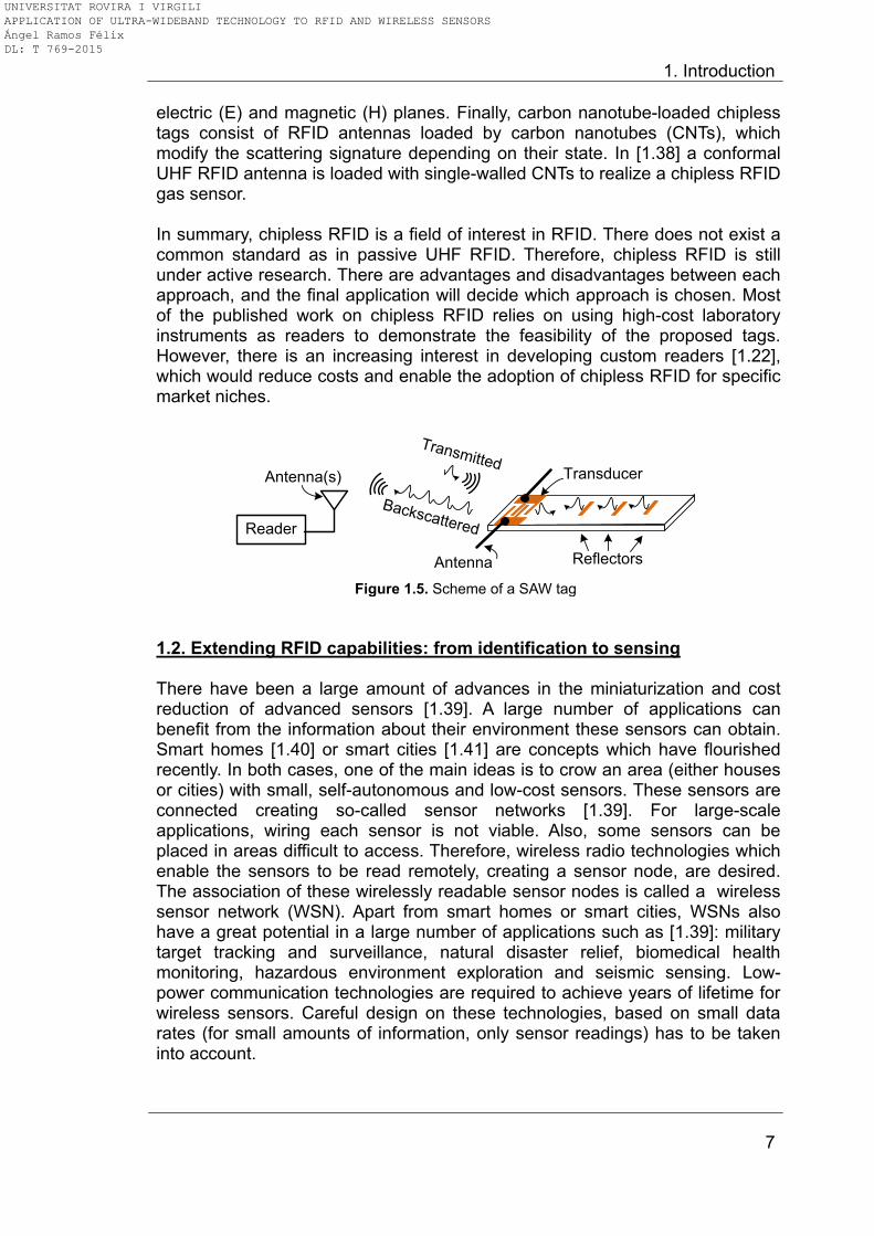
Sensor nodes and readers (or reading points, RP) can be associated in several manners. A direct wireless link between each sensor and RP (see Figure 1.6a, centralized „star‟ topology) is a solution that requires high RF power transmitters if distances are long, with consequent impact on batteries lifetime or the need for power supply each sensor. A second possibility is to link the sensors in what is called a wireless network. In this way, the sensors also act as a bridge for other sensors (see Figure 1.6b, mesh topology). A third solution might be the use of a mobile link between sensors and RP (see Figure 1.6c, mobile topology). This means to take advantage of the mobility of vehicles inside a city to use them to also transport information. For instance (see Figure 1.6d), buses can be good candidates. A bus performs always the same route, and stops periodically and repeatedly in bus stops. If a wireless sensor is installed in a bus stop and the reader at the bus, the sensor can be read every time the bus stops there. The information recorded in each traject can be downloaded at a point (normally another bus stop) which is connected to the data management point. The main advantage of this solution is that low-power consumption wireless sensors can be used, since read ranges are in the order of few meters, enhancing their autonomy.
-a-
-b-
-c-
Temperature
Acceleartion
Pressure
Humidity
Gas
-d-
Figure 1.6. Sensors: green points. Reader point (RP): red point. (a) Centralized topology, (b) Mesh topology, (c) Mobile RP topology, (d) scheme of transmission between the bus and the
bus-station
1.2.1. Existing technologies for wireless sensor networks
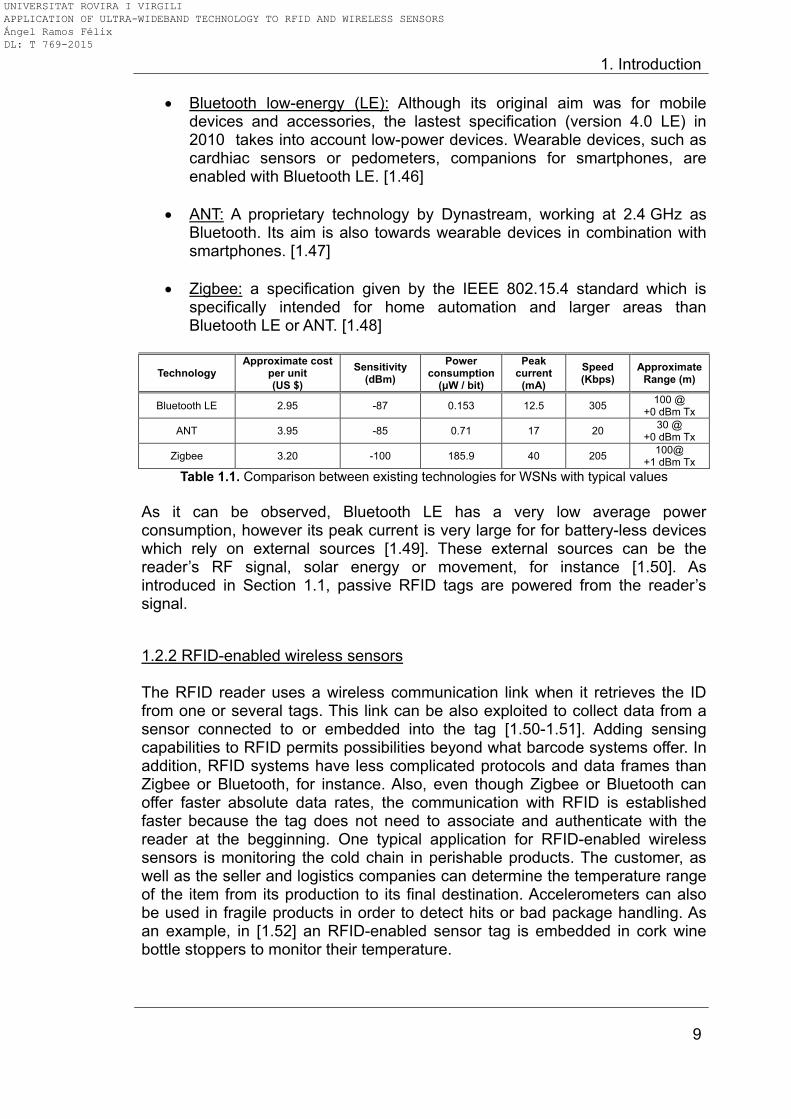
There are several commercial low-power solutions existing in the market for wireless sensor networks [1.42-1.45]. Next, some of the most popular solutions are compared in terms of cost, power consumption, speed and range. Table 1.1 summarizes typical values of these parameters for Bluetooth low-energy, ANT and Zigbee technologies. Other technologies such as WiFi (IEEE 802.11), NFC, or infrared (IrDA) [1.42] were discarded in this comparison because they are not intented for wireless sensor applications. Therefore, either their power consumption is extremely high for miniaturized portable devices (WiFi) or their read range is very short for a wireless sensor (NFC or IrDA).
UNIVERSITAT ROVIRA I VIRGILI APPLICATION OF ULTRA-WIDEBAND TECHNOLOGY TO RFID AND WIRELESS SENSORS Ángel Ramos Félix DL: T 769-2015
1. Introduction
9
Bluetooth low-energy (LE): Although its original aim was for mobile devices and accessories, the lastest specification (version 4.0 LE) in 2010 takes into account low-power devices. Wearable devices, such as cardhiac sensors or pedometers, companions for smartphones, are enabled with Bluetooth LE. [1.46]
ANT: A proprietary technology by Dynastream, working at 2.4 GHz as Bluetooth. Its aim is also towards wearable devices in combination with smartphones. [1.47]
Zigbee: a specification given by the IEEE 802.15.4 standard which is specifically intended for home automation and larger areas than Bluetooth LE or ANT. [1.48]
Technology Approximate cost
per unit (US $)
Sensitivity (dBm)
Power consumption
(μW / bit)
Peak current
(mA)
Speed (Kbps)
Approximate Range (m)
Bluetooth LE 2.95 -87 0.153 12.5 305 100 @
+0 dBm Tx
ANT 3.95 -85 0.71 17 20 30 @
+0 dBm Tx
Zigbee 3.20 -100 185.9 40 205 100@
+1 dBm Tx
Table 1.1. Comparison between existing technologies for WSNs with typical values
As it can be observed, Bluetooth LE has a very low average power consumption, however its peak current is very large for for battery-less devices which rely on external sources [1.49]. These external sources can be the reader‟s RF signal, solar energy or movement, for instance [1.50]. As introduced in Section 1.1, passive RFID tags are powered from the reader‟s signal.
1.2.2 RFID-enabled wireless sensors The RFID reader uses a wireless communication link when it retrieves the ID from one or several tags. This link can be also exploited to collect data from a sensor connected to or embedded into the tag [1.50-1.51]. Adding sensing capabilities to RFID permits possibilities beyond what barcode systems offer. In addition, RFID systems have less complicated protocols and data frames than Zigbee or Bluetooth, for instance. Also, even though Zigbee or Bluetooth can offer faster absolute data rates, the communication with RFID is established faster because the tag does not need to associate and authenticate with the reader at the begginning. One typical application for RFID-enabled wireless sensors is monitoring the cold chain in perishable products. The customer, as well as the seller and logistics companies can determine the temperature range of the item from its production to its final destination. Accelerometers can also be used in fragile products in order to detect hits or bad package handling. As an example, in [1.52] an RFID-enabled sensor tag is embedded in cork wine bottle stoppers to monitor their temperature.
UNIVERSITAT ROVIRA I VIRGILI APPLICATION OF ULTRA-WIDEBAND TECHNOLOGY TO RFID AND WIRELESS SENSORS Ángel Ramos Félix DL: T 769-2015
Application of Ultra-Wideband Technology to RFID and Wireless Sensors
10
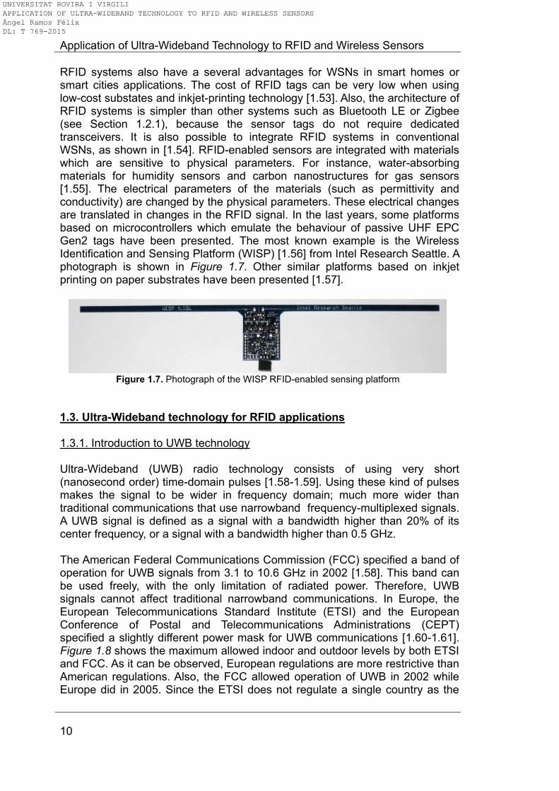
RFID systems also have a several advantages for WSNs in smart homes or smart cities applications. The cost of RFID tags can be very low when using low-cost substates and inkjet-printing technology [1.53]. Also, the architecture of RFID systems is simpler than other systems such as Bluetooth LE or Zigbee (see Section 1.2.1), because the sensor tags do not require dedicated transceivers. It is also possible to integrate RFID systems in conventional WSNs, as shown in [1.54]. RFID-enabled sensors are integrated with materials which are sensitive to physical parameters. For instance, water-absorbing materials for humidity sensors and carbon nanostructures for gas sensors [1.55]. The electrical parameters of the materials (such as permittivity and conductivity) are changed by the physical parameters. These electrical changes are translated in changes in the RFID signal. In the last years, some platforms based on microcontrollers which emulate the behaviour of passive UHF EPC Gen2 tags have been presented. The most known example is the Wireless Identification and Sensing Platform (WISP) [1.56] from Intel Research Seattle. A photograph is shown in Figure 1.7. Other similar platforms based on inkjet printing on paper substrates have been presented [1.57].
Figure 1.7. Photograph of the WISP RFID-enabled sensing platform
1.3. Ultra-Wideband technology for RFID applications 1.3.1. Introduction to UWB technology
Ultra-Wideband (UWB) radio technology consists of using very short (nanosecond order) time-domain pulses [1.58-1.59]. Using these kind of pulses makes the signal to be wider in frequency domain; much more wider than traditional communications that use narrowband frequency-multiplexed signals. A UWB signal is defined as a signal with a bandwidth higher than 20% of its center frequency, or a signal with a bandwidth higher than 0.5 GHz.
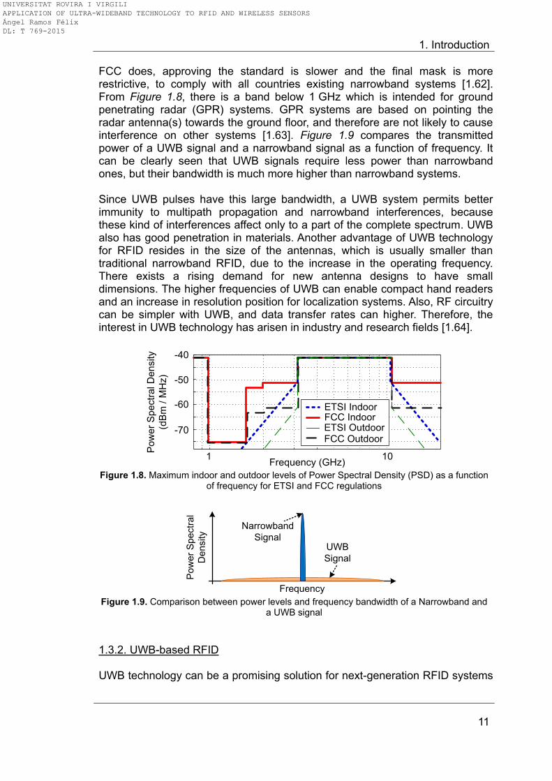
The American Federal Communications Commission (FCC) specified a band of operation for UWB signals from 3.1 to 10.6 GHz in 2002 [1.58]. This band can be used freely, with the only limitation of radiated power. Therefore, UWB signals cannot affect traditional narrowband communications. In Europe, the European Telecommunications Standard Institute (ETSI) and the European Conference of Postal and Telecommunications Administrations (CEPT) specified a slightly different power mask for UWB communications [1.60-1.61]. Figure 1.8 shows the maximum allowed indoor and outdoor levels by both ETSI and FCC. As it can be observed, European regulations are more restrictive than American regulations. Also, the FCC allowed operation of UWB in 2002 while Europe did in 2005. Since the ETSI does not regulate a single country as the
UNIVERSITAT ROVIRA I VIRGILI APPLICATION OF ULTRA-WIDEBAND TECHNOLOGY TO RFID AND WIRELESS SENSORS Ángel Ramos Félix DL: T 769-2015
1. Introduction
11
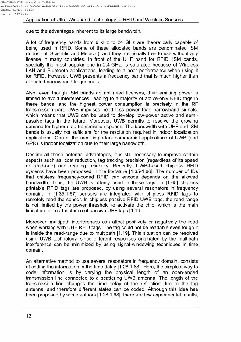
FCC does, approving the standard is slower and the final mask is more restrictive, to comply with all countries existing narrowband systems [1.62]. From Figure 1.8, there is a band below 1 GHz which is intended for ground penetrating radar (GPR) systems. GPR systems are based on pointing the radar antenna(s) towards the ground floor, and therefore are not likely to cause interference on other systems [1.63]. Figure 1.9 compares the transmitted power of a UWB signal and a narrowband signal as a function of frequency. It can be clearly seen that UWB signals require less power than narrowband ones, but their bandwidth is much more higher than narrowband systems.
Since UWB pulses have this large bandwidth, a UWB system permits better immunity to multipath propagation and narrowband interferences, because these kind of interferences affect only to a part of the complete spectrum. UWB also has good penetration in materials. Another advantage of UWB technology for RFID resides in the size of the antennas, which is usually smaller than traditional narrowband RFID, due to the increase in the operating frequency. There exists a rising demand for new antenna designs to have small dimensions. The higher frequencies of UWB can enable compact hand readers and an increase in resolution position for localization systems. Also, RF circuitry can be simpler with UWB, and data transfer rates can higher. Therefore, the interest in UWB technology has arisen in industry and research fields [1.64].
Frequency (GHz)1 10
-40
-50
-60
-70
Po
we
r S
pe
ctr
al D
en
sity
(dB
m /
MH
z)
ETSI IndoorFCC IndoorETSI OutdoorFCC Outdoor
Figure 1.8. Maximum indoor and outdoor levels of Power Spectral Density (PSD) as a function
of frequency for ETSI and FCC regulations
Frequency
Pow
er
Sp
ectr
al
Den
sity
UWB
Signal
Narrowband
Signal
Figure 1.9. Comparison between power levels and frequency bandwidth of a Narrowband and
a UWB signal
1.3.2. UWB-based RFID
UWB technology can be a promising solution for next-generation RFID systems
UNIVERSITAT ROVIRA I VIRGILI APPLICATION OF ULTRA-WIDEBAND TECHNOLOGY TO RFID AND WIRELESS SENSORS Ángel Ramos Félix DL: T 769-2015
Application of Ultra-Wideband Technology to RFID and Wireless Sensors
12
due to the advantages inherent to its large bandwitdh. A lot of frequency bands from 9 kHz to 24 GHz are theoretically capable of being used in RFID. Some of these allocated bands are denominated ISM (Industrial, Scientific and Medical), and they are usually free to use without any license in many countries. In front of the UHF band for RFID, ISM bands, specially the most popular one in 2.4 GHz, is saturated because of Wireless LAN and Bluetooth applications, leading to a poor performance when using it for RFID. However, UWB presents a frequency band that is much higher than allocated narrowband frequencies.
Also, even though ISM bands do not need licenses, their emitting power is limited to avoid interferences, leading to a majority of active-only RFID tags in these bands, and the highest power consumption is precisely in the RF transmission part. UWB impulses need less power than narrowband signals, which means that UWB can be used to develop low-power active and semi-passive tags in the future. Moreover, UWB permits to resolve the growing demand for higher data transmission speeds. The bandwidth with UHF and ISM bands is usually not sufficient for the resolution required in indoor localization applications. One of the most important commercial applications of UWB (and GPR) is indoor localization due to their large bandwidth. Despite all these potential advantages, it is still necessary to improve certain aspects such as: cost reduction, tag tracking precision (regardless of its speed or read-rate) and reading reliability. Recently, UWB-based chipless RFID systems have been proposed in the literature [1.65-1.66]. The number of IDs that chipless frequency-coded RFID can encode depends on the allowed bandwidth. Thus, the UWB is oftenly used in these tags. In [1.65] chipless printable RFID tags are proposed, by using several resonators in frequency domain. In [1.35,1.67] sensors are integrated with chipless RFID tags to remotely read the sensor. In chipless passive RFID UWB tags, the read-range is not limited by the power threshold to activate the chip, which is the main limitation for read-distance of passive UHF tags [1.19].
Moreover, multipath interferences can affect positively or negatively the read when working with UHF RFID tags. The tag could not be readable even tough it is inside the read-range due to multipath [1.19]. This situation can be resolved using UWB technology, since different responses originated by the multipath interference can be minimized by using signal-windowing techniques in time domain. An alternative method to use several resonators in frequency domain, consists of coding the information in the time delay [1.28,1.68]. Here, the simplest way to code information is by varying the physical length of an open-ended transmission line connected to a scattering UWB antenna. The length of the transmission line changes the time delay of the reflection due to the tag antenna, and therefore different states can be coded. Although this idea has been proposed by some authors [1.28,1.68], there are few experimental results,
UNIVERSITAT ROVIRA I VIRGILI APPLICATION OF ULTRA-WIDEBAND TECHNOLOGY TO RFID AND WIRELESS SENSORS Ángel Ramos Félix DL: T 769-2015
1. Introduction
13
which have been obtained by means of high-cost instruments such as vector network analyzers (VNA). Future implementations of commercial readers should be based on low-cost equipments, such as impulse radio (IR) UWB radars. 1.4. Objectives of this Doctoral Thesis There is a lot of research towards creating compact RFID-enabled wireless sensors for the Internet of Things. In addition, some applications also require to localize these sensors in an indoor scenario. Time-domain UWB is an interesting alternative which can be exploited in that direction. In consequence, the objectives of this Doctoral Thesis are to:
Propose a model to understand the operation of RFID based on time-domain UWB technology
Study of the feasibility of chipless RFID based on time-domain UWB technology
Study wireless chipless sensors based on chipless RFID time-domain UWB tags
Design semi-passive and active RFID alternative platforms based on time-domain UWB technology for identification, sensing and indoor localization
Explore some possible applications with the developed chipless, semi-passive and active platforms
1.5. Organization of this document The document is organized as follows:
Chapter 2 describes the chipless time-coded UWB RFID theory, signal processing techniques and reader alternatives. Then, chipless tags are designed and characterized. Read range, resolution (number of bits), influence of angle, polarization and materials is studied. Finally, the effect of bending in flexible tag prototypes is studied when manufactured on flexible substrates.
Chapter 3 uses Chapter 2 foundations and tags to design chipless sensors. Amplitude-based (continuous and threshold temperature) and delay-based (permittivity for concrete composition detection) chipless sensors are proposed.
Chapter 4 presents two semi-passive (analog and digital) wireless
UNIVERSITAT ROVIRA I VIRGILI APPLICATION OF ULTRA-WIDEBAND TECHNOLOGY TO RFID AND WIRELESS SENSORS Ángel Ramos Félix DL: T 769-2015
Application of Ultra-Wideband Technology to RFID and Wireless Sensors
14
sensing platforms based on time-coded UWB RFID.
Chapter 5 integrates temperature and gas sensors in the semi-passive sensing platforms proposed in Chapter 4.
Chapter 6 proposes a smart floor application with the chipless (Chapter 2) and semi-passive (Chapter 4) tags, combined with ground penetrating radar technology.
Chapter 7 presents active long-range platforms based on time-coded UWB RFID, intended for localization applications.
Finally, Chapter 8 is the result of a collaboration work between Universitat Rovira i Virgili in Tarragona, Spain (institution where the Thesis has been carried out) and Grenoble Institute of Technology - LCIS in Valence, France. A signal processing technique is studied in order to detect frequency-coded chipless tags previously developed at LCIS.
1.6. Bibliography
[1.1] W. Loeb, “10 Reasons Why Alibaba Blows Away Amazon And Ebay,” Forbes (Retail),
Nov. 4, 2014.
[1.2] R. C. Palmer, “The Bar Code Book: Fifth Edition - A Comprehensive Guide To Reading, Printing, Specifying, Evaluating, And Using Bar Code and Other Machine-Readable Symbols,” Trafford Publishing, 2007.
[1.3] Denso Wave, “What is a QR Code?,” http://www.qrcode.com/en/about/ Nov. 2014 [Nov.
20, 2014]
[1.4] E. Ohbuchi, H. Hanaizumi, and L. A. Hock, “Barcode readers using the camera device in mobile phones,” 2004 International Conference on Cyberworlds, pp. 260-265, 18-20 Nov. 2004.
[1.5] K. Finkenzeller, “RFID Handbook: Fundamentals and Applications in Contactless Smart
Cards, Radio Frequency Identification and Near-Field Communication”, Wiley 3rd
Ed., 2010.
[1.6] R. Want, “An Introduction to RFID Technology,” IEEE Pervasive Computing, Vol. 5,
No. 1, pp. 25-33, 2006.
[1.7] P. Harrop, R. Das, and G. Holland, "Near Field Communication (NFC) 2014-2024 - Mobile phone and other NFC: market forecasts, technology, players," IDTechEx, 2014.
[1.8] G. D. Vita and G. Iannaccone, “Design criteria for the RF section of UHF and
microwave passive RFID transponders,” IEEE Transactions on Microwave Theory and Tech., Vol. 53, No. 9, pp. 2978-2990, 2005.
[1.9] J. Collins, “Alien cuts tag price,” RFID Journal, April 2004.
[1.10] GS1, "Regulatory status for using RFID in the EPC Gen 2 band (860 to 960 MHz) of the
UHF spectrum," http://www.gs1.org/docs/epcglobal/UHF_Regulations.pdf, Oct. 2014 [Jan. 24, 2014].
UNIVERSITAT ROVIRA I VIRGILI APPLICATION OF ULTRA-WIDEBAND TECHNOLOGY TO RFID AND WIRELESS SENSORS Ángel Ramos Félix DL: T 769-2015
1. Introduction
15
[1.11] Impinj Inc., "Monza R6 RFID Tag Chip," http://www.impinj.com/products/tag-
chips/monza-r6/, 2014 [Nov. 25, 2014].
[1.12] Alien Technology LLC, "Higgs(R) 4 RFID IC," http://www.alientechnology.com/wp-content/uploads/ALC-370-SOT%20Higgs4%20SOT%202014-12-21.pdf, 2014 [Nov. 25, 2014].
[1.13] Extronics, Omni ID, "RFID Tag Comparison Guide," http://www.extronics.com/media/234005/rfid_tag_comparison_broadband_whitepaper.pdf, Aug. 2010 [Jan 12, 2012].
[1.14] Y. C. Zheng, G. Hua, Y. L. Zheng, and W. Hong, "Design of a miniaturized RFID tag antenna with BAP technique," 2014 3rd Asia-Pacific Conference on Antennas and Propagation, pp. 256-258, 2014.
[1.15] P. Pursula, T. Vaha-Heikkila, A. Muller, D. Neculoiu, G. Konstantinidis, A. Oja, and J. Tuovinen, "Millimeter-Wave Identification - A New Short-Range Radio System for Low-Power High Data-Rate Applications," IEEE Transactions on Microwave Theory and Techniques, Vol. 56, No. 10, pp. 2221-2228, 2008.
[1.16] H. C. Gomes and N. B. Carvalho, "The use of intermodulation distortion for the design of passive RFID," Proc. European Microwave Conference 2007, pp. 1656-1659, 2007.
[1.17] V. Viikari and H. Seppa, "RFID MEMS Sensor Concept Based on Intermodulation Distortion," IEEE Sensors Journal, Vol. 9, No. 12, 2009.
[1.18] A. Lazaro, D. Girbau, and R. Villarino, “Effects of interferences in UHF RFID Systems”,
Progress in Electromagnetics Research, PIER, Vol. 98, pp. 435-443, 2009.
[1.19] A. Lazaro, D. Girbau, and D. Salinas, “Radio link budgets for UHF RFID on multipath environments,” IEEE Transactions on Antennas and Propagation, Vol. 57, No. 4, pp. 1241-1251, 2009.
[1.20] J. Lorenzo, D. Girbau, A. Lazaro, and R. Villarino, “Read range reduction in UHF RFID
due to antenna detuning and gain penalty,” Microwave and Optical Technology Letters, Vol. 53, No. 1, pp. 144-148, 2011.
[1.21] S. Preradovic and N. C. Karmakar, “Chipless RFID: Bar Code of the Future,” IEEE
Microwave Magazine, Vol. 11, No. 7, pp. 87-97, 2010.
[1.22] S. Tedjini, N. C. Karmakar, E. Perret, A. Vena, R. Koswatta, and R. E-Azim, “Hold the Chips: Chipless Technology, an Alternative Technique for RFID,” IEEE Microwave Magazine, Vol 14, No. 5, pp. 56-65, 2013.
[1.23] C. S. Hartmann, “A global SAW ID tag with large data capacity,” Proc. IEEE Ultrason.
Symp., Vol. 1, pp. 65–69, Munich, Germany, October 2002.
[1.24] L. Reindl, et al., “Theory and Application of Passive SAW Radio Transponders as Sensors,” IEEE Transactions on Ultrasonics, Ferroelectrics, and Frequency Control, Vol. 45, No. 5, pp. 1281-1292, September 1998.
[1.25] L. Reindl, et al., “Design, Fabrication, and Application of Precise SAW Delay Lines Used
in an FMCW Radar System,” IEEE Transactions on Microwave Theory and Techniques, Vol. 49, No. 4, pp. 787-794, April 2001.
[1.26] R. Das and P. Harrop, “Chipl-ess RFID forecasts, technologies & players 2006-2016,”
IDTech, March 2006.
UNIVERSITAT ROVIRA I VIRGILI APPLICATION OF ULTRA-WIDEBAND TECHNOLOGY TO RFID AND WIRELESS SENSORS Ángel Ramos Félix DL: T 769-2015

Application of Ultra-Wideband Technology to RFID and Wireless Sensors
16
[1.27] S. Shretha, J. Vemagiri, M. Agarwal, and K. Varahramyan, “Transmission line delay-
based radio frequency identification (RFID) tag,” Mirowave and Optical Technology Letters, Vol. 49, No. 8, pp. 1900-1904, 2007.
[1.28] S. Hu, Y. Zhou, C. L. Law, and W. Dou, “Study of a Uniplanar Monopole Antenna for
Passive Chipless UWB-RFID Localization System,” IEEE Transactions on Antennas and Propagation, Vol. 58, No. 2, pp. 271-278, February 2010.
[1.29] J. Collins, “RFID fibers for secure applications,” RFID Journal, 2006.
[1.30] K. C. Jones, “Invisible RFID Ink Safe For Cattle And People, Company Says,”
Information Week, Jan. 10, 2007.
[1.31] I. Jalaly and I. D. Robertson, “RF bar codes using multiple frequency bands,” Proc. IEEE MTT-S Int. Microwave Symp. Dig. 2005, pp. 4-7, Jun 2005.
[1.32] J. McVay, A. Hoorfar, and N. Engheta, “Space-filling curve RFID tags,” 2006 IEEE Radio
and Wireless Symp. Dig., pp. 199-202, Jan. 2006.
[1.33] R. R. Fletcher, "Low-Cost Electromagnetic Tagging: Design and Implementation," Massachusetts Institute of Technology degree of Doctor of Philosophy in Media, Arts and Sciences, Sep. 2002.
[1.34] A. Vena, E. Perret, and S. Tedjini, “A Depolarizing Chipless RFID Tag for Robust
Detection and Its FCC Compliant UWB Reading System,” IEEE Transactions on Microwave Theory and Techniques, Vol. 61, No. 8, pp. 2982-2994, Aug. 2013.
[1.35] M. Schuler, C. Mandel, M. Maasch, A. Giere, and R. Jakoby, “Phase modulation
scheme for chipless RFID- and wireless sensor tags,” Proc. Asia Pacific Microwave Conf. 2009, pp. 229-232, Dec. 2009.
[1.36] S. Mukherjee, “Chipless radio frequency identification by remote measurement of
complex impedance,” Proc. 37th European Microwave Conf., pp. 1007–1010, Oct. 2007.
[1.37] I. Balbin and N. C. Karmakar, “Phase-encoded chipless RFID transponder for large-
scale low-cost applications,” IEEE Microwave and Wireless Components Letters, Vol. 19, No. 8, pp. 509-511, 2009.
[1.38] L. Yang, R. Zhang, D. Staiculescu, C. P. Wong, and M. M. Tentzeris, "A Novel
Conformal RFID-Enabled Module Utilizing Inkjet-Printed Antennas and Carbon Nanotubes for Gas-Detection Applications," IEEE Antennas and Wireless Propagation Letters, Vol. 8, pp. 653-656, 2009.
[1.39] J. Yick, B. Mukherjee, and D. Ghosal, "Wireless sensor network survey," Computer
Networks, Vol. 52, pp. 2292-2330, 2008.
[1.40] S. Helal, W. Mann, H. El-Zabadani, J. King, Y. Kaddoura, and E. Jansen, "The Gator Tech Smart House: A Programmable Pervasive Space," Computer, Vol. 38, No. 3, pp. 50-60, 2005.
[1.41] M. Naphade, G. Banavar, C. Harrison, J. Paraszczak, and R. Morris, "Smarter Cities
and Ther Innovation Challenges," Computer, Vol. 44, No. 6, pp. 32-39, 2011.
[1.42] P. Smith, "Comparing Low-Power Wireless Technologies," Digikey ArticleLibrary - Convergence Promotions LLC, Aug. 8, 2011.
UNIVERSITAT ROVIRA I VIRGILI APPLICATION OF ULTRA-WIDEBAND TECHNOLOGY TO RFID AND WIRELESS SENSORS Ángel Ramos Félix DL: T 769-2015

1. Introduction
17
[1.43] V. C. Gungor and G. P. Hancke, "Industrial Wireless Sensor Networks: Challenges, Design Principles, and Technical Approaches," IEEE Transactions on Industrial Electronics, Vol. 56, No. 10, pp. 4258-4265, 2009.
[1.44] Texas Instruments, "Wireless Connectivity," http://www.ti.com/lit/sg/slab056d/slab056d.pdf 2014 [Jan. 23, 2015].
[1.45] A. Dementyev, S. Hodges, S. Taylor, and J. Smith, "Power consumption analysis of Bluetooth Low Energy, ZigBee and ANT sensor nodes in a cyclic sleep scenario," 2013 IEEE International Wireless Symposium, pp. 1-4, 2013.
[1.46] R. Want, B. Schilit, and D. Laskowski, "Bluetooth LE Finds Its Niche," IEEE Pervasive
Computing, Vol. 12, No. 4, pp. 12-16, 2013.
[1.47] Dynastream Innovations Inc., “This is ANT”, http://www.thisisant.com/, Jan. 2015 [Jan. 23, 2015]
[1.48] A. Wheeler, "Commercial Applications of Wireless Sensor Networks Using Zigbee,"
IEEE Communications Magazine, Vol. 45, No. 4, pp. 70-77, 2007.
[1.49] J. A. Paradiso and T. Starner, “Energy scavenging for mobile and wireless electronics,” IEEE Pervasive Computing, Vol. 4, No. 11, pp. 18-27, 2005.
[1.50] S. Kim, C. Mariotti, F. Alimenti, P. Mezzanotte, A. Georgiadis, A. Collado, L. Roselli, and
M. M. Tentzeris, "No Battery Required: Perpetual RFID-Enabled Wireless Sensors for Cognitive Intelligence Applications," IEEE Microwave Magazine, Vol. 14, No. 5, pp. 66-77, 2013.
[1.51] R. Want, "Enabling Ubiquitous Sensing with RFID," Computer, Vol. 37, No. 4, pp. 84-86,
2004.
[1.52] R. Goncalves, S. Rima, R. Magueta, A. Collado, P. Pinho, N. B. Carvalho, and A. Georgiadis, “RFID tags on cork stoppers for bottle identification,” IEEE MTT-S International Microwave Symposium 2014, pp. 1-4, 2014.
[1.53] S. Molesa, D. R. Redinger, D. C. Huang, and V. Subramanian, “High-quality ink-jet-
printed multilevel interconnects and inductive components on plastic for ultra-low-cost RFID applications,” Proc. MRS 2003, Vol. 769, pp. H8.3, 2003.
[1.54] H. Liu, M. Bolic, A. Nayak, and I. Stojmenovic, “Taxonomy and challenges of the
integration of RFID and wireless sensor networks,” IEEE Network, Vol. 22, No. 6, pp. 26–35, 2008.
[1.55] A. Vena, L. Sydänheimo, M. M. Tentzeris, and L. Ukkonen, “A Novel Inkjet Printed
Carbon Nanotube-Based Chipless RFID Sensor for Gas Detectionk,” Proc. of the 43rd European Microwave Conference, 2013.
[1.56] A. P. Sample, D. J. Yeager, S. P. Powledge, A. V. Mamishev, and J. R. Smith, “Design of
an RFID-Based Battery-Free Programmable Sensing Platform,” IEEE Transactions on Instrumentation and Measurement, Vol. 57, No. 11, pp. 2608-2615, 2008.
[1.57] R. Vykas, V. Lakafosis, A. Rida, N. Chaisilwattana, S. Travis, J. Pan, and M. M.
Tentzeris, “Paper-Based RFID-Enabled Wireless Platforms for Sensing Applications,” IEEE Transactions on Microwave Theory and Techniques, Vol. 57, No. 5, pp. 1370-1382, 2009.
[1.58] FCC Notice of Proposed Rule Making, “Revision of Part 15 of the Commision‟s Rules
Regarding Ultra-wideband Transmission Systems”, ET-Docket 98-153.
UNIVERSITAT ROVIRA I VIRGILI APPLICATION OF ULTRA-WIDEBAND TECHNOLOGY TO RFID AND WIRELESS SENSORS Ángel Ramos Félix DL: T 769-2015
Application of Ultra-Wideband Technology to RFID and Wireless Sensors
18
[1.59] S. Jose, “Design of RF CMOS Power Amplifier for UWB Applications”, Virginia
Polytechnic Institute and State University, 2004.
[1.60] ETSI EN 302 065 V1.1.1 (2008-02), “Electromagnetic compatibility and Radio spectrum Matters (ERM); Ultra WideBand (UWB) technologies for communication purposes; Harmonized EN covering the essential requirements of article 3.2 of the R&TTE Directive,” February 2008.
[1.61] A. W. Astrin, H.-B. Li, and R. Kohno, “Standardization for body area networks”, IEICE
Trans. Commun., Vol. E92-B, No. 2, pp.366-372, Feb. 2009.
[1.62] H. Mazar, "A comparison between European and North American wireless regulations," 2011 Technical Symposium at ITU Telecom World, pp. 182-186, 2011.
[1.63] D. J. Daniels, “Ground penetrating radar”, John Wiley & Sons, Inc., 2005.
[1.64] R. J. Fontana, “Recent system applications of short-pulse ultra-wideband (UWB)
technology,” IEEE Transactions on Microwave Theory and Techniques, Vol. 52, No. 9, pp. 2087–2104, 2004.
[1.65] I. Balbin and N. Karmakar, “Novel Chipless RFID Tag for Conveyor Belt Tracking using
Multi-Resonant Dipole Antenna”, Proceedings of the 39th European Microwave Conference, pp. 1109-1112, 2009.
[1.66] L. Zhang, S. Rodriguez, H. Tenhunen, and L. R. Zheng, “An Innovative Fully Printable
RFID Technology Based on High Speed Time-Domain Reflection”, Conference on High Density Microsystem Design and Packaging and Component Failure Analysis, pp. 166-170, 2006.
[1.67] J. Dowling and M. M. Tentzeris, “"Smart House" and "Smart-Energy" Applications of
Low-Power RFID-based Wireless Sensors”, IEEE Asia Microwave Conference 2009, pp. 2412-2415, 2009.
[1.68] D. Dardari and R. D'Errico, “Passive Ultrawide Bandwidth RFID”, IEEE Global
Telecommunications Conference (GLOBECOM), 1–6, 2008.
UNIVERSITAT ROVIRA I VIRGILI APPLICATION OF ULTRA-WIDEBAND TECHNOLOGY TO RFID AND WIRELESS SENSORS Ángel Ramos Félix DL: T 769-2015
2. Chipless Time-Coded UWB RFID
19
2. Chipless Time-Coded UWB RFID 2.1. Introduction Chipless time-coded UWB RFID could be an alternative for RFID systems. The tag’s ID is coded in the physical length of an open-ended transmission line connected to a scattering UWB antenna. Although this idea has been proposed by some authors [2.1-2.4], there are few experimental results, which have been obtained by means of expensive instruments such as vector network analyzers (VNA). Future implementations of commercial readers should be based on low-cost equipments, such as impulse radio (IR) UWB radars [2.5-2.7]. Due to their large bandwidth, a small signal-to-noise ratio is expected with these systems. Therefore, signal processing techniques should be considered in order to detect the tag in a real scenario with noise. Finally, the realization (integrating a UWB antenna with a long delay) and characterization of chipless time-coded UWB tags should be studied in detail. In this chapter, the following fields are addressed:
Section 2.2 presents the theoretical foundations
Section 2.3 compares two reader approaches
Section 2.4 presents the signal processing techniques used to improve the detection in real scenarios
Section 2.5 studies the design of tags in terms of integration of UWB antennas and delay lines
Section 2.6 characterizes the designed tags in terms of the materials attached, tag-reader angle, polarization and bending
Finally, Section 2.7 draws the conclusions of the chapter 2.2. Theory Passive RFID is based on modulating the radar cross section [2.8] of the tag. Depending on the authors (Green [2.9], Collin [2.10], Hansen [2.11]), there are different formulations for deriving the scattered field at an antenna connected to an arbitrary load, when the antenna is illuminated by a plane wave. However, these authors have shown that this field can be expressed as the sum of two terms (or modes):
A structural mode Esm, which is mainly due to the wave diffraction at the antenna structure (patches, ground plane, edge effects…)
An antenna mode (or tag mode) Eam, which is mainly due to the radiation properties of the antenna. This term depends on the load ZL connected to the antenna
In consequence, the scattered field ES(ZL) at an antenna connected to an
arbitrary load ZL can be obtained from [2.12-2.13], and expressed as:
UNIVERSITAT ROVIRA I VIRGILI APPLICATION OF ULTRA-WIDEBAND TECHNOLOGY TO RFID AND WIRELESS SENSORS Ángel Ramos Félix DL: T 769-2015
Application of Ultra-Wideband Technology to RFID and Wireless Sensors
20
0( ) ( ) ( ) ( )1
S sm am sm LL c L c
L a
E Z E Z E Z E Z E
, (2.1)
where Esm
(Zc) is the structural-mode scattering field and Eam(ZL) = E0ΓL /(1- ΓL Γa)
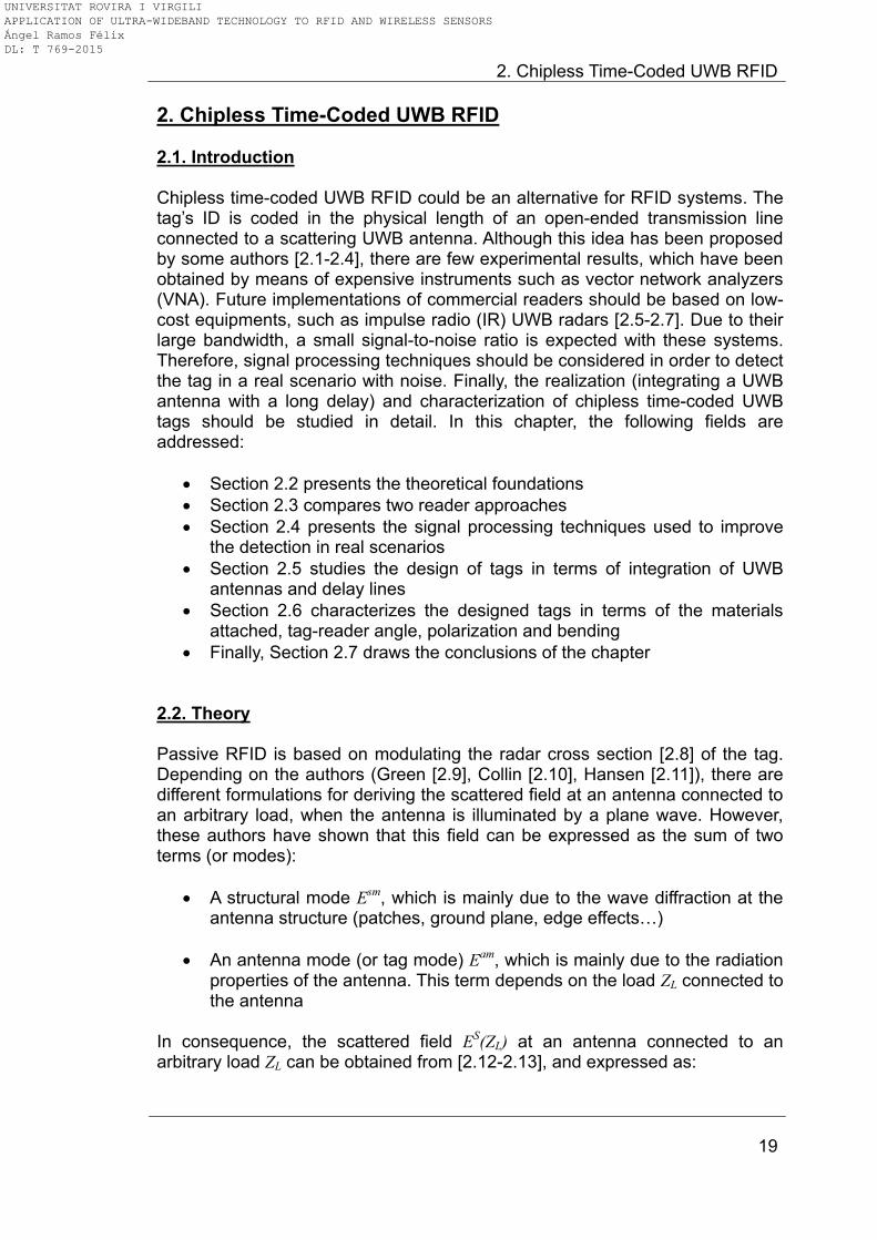
is the antenna-mode (or tag-mode) scattering field. Zc is the normalization impedance, E0 is the scattering field under an unit incident wave and Γa, ΓL are the reflection coefficients of the antenna and the load, respectively. The reflection coefficient ΓL, which multiplies the unit-incident-wave scattering field E0, depends on the circuit connected to the antenna. This circuit not only accounts for the load itself (ZLOAD), but also for the transmission line that connects the antenna and the load. Therefore, the antenna-mode scattering field depends on the load and on the length L of this transmission line. When the circuit connected to the antenna is matched (ΓL = 0) only structural scattering exists. If not, part of the received energy is reradiated, and structural and antenna modes coexist. The full RFID scheme is shown in Figure 2.1a, and a scheme of the structural and tag modes is shown in Figure 2.1b. The transmitter (Tx) illuminates the tag. When the transmitted pulse hits the tag antenna, a portion is backscattered towards the receiver (Rx) and a portion propagates inside the tag. Then, time-coded chipless tags can be considered scattering antennas (antennas terminated with a load impedance) with two scattering modes: the structural mode (first or early-time reflection) and the tag (or antenna) mode (second reflection). Also, coupling from Tx antenna to Rx antenna has to be considered, since both antennas cannot be perfectly isolated from each other in a real-case scenario.
Tag UWB
Antenna
L
L
Transmission
Line
Time
Structural
Mode
Tag
Mode
Time
p(t)
2L/v
Reader
Tx UWB
Antenna
Coupling
Rx UWB
Antenna
Tag
Mode
Structural
Mode
Open
Circuit
LOAD
(Zc)
TAG ID
-a-
Transmission
Line
Antenna
Structural Mode Tag Mode
L
Tag
-b-
Figure 2.1. (a) Time-coded UWB RFID system scheme. (b) Scheme of the structural and tag modes
UNIVERSITAT ROVIRA I VIRGILI APPLICATION OF ULTRA-WIDEBAND TECHNOLOGY TO RFID AND WIRELESS SENSORS Ángel Ramos Félix DL: T 769-2015
2. Chipless Time-Coded UWB RFID
21
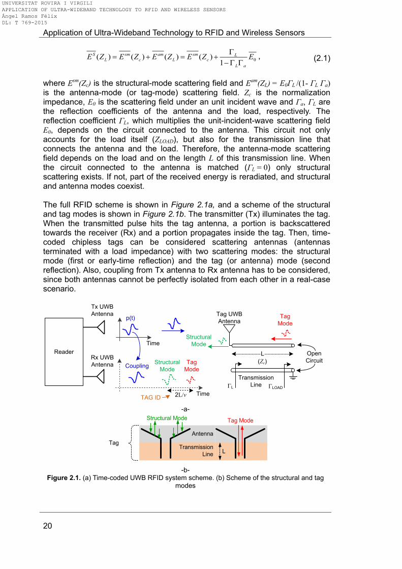
The tag is modelled as an equivalent two-port network (antenna) terminated with a transmission line of length L and characteristic impedance Zc. The line is in turn loaded with an impedance ZLOAD [2.10], as presented in Figure 2.2. The wave ain represents the incoming wave from the reader. The outcoming wave bout is generated due to reflection and is scattered in direction to the reader. Wave cpl represents the coupling from the reader transmitting to receiving antennas. The waves ain and bout are normalized to the free-space impedance (120π Ω). The output of the antenna is normalized to Zc. Thus, S22a in Figure 2.2b represents the reflection coefficient of the antenna, S22a = Γa. The reflection coefficients Γa and ΓL are defined as (2.2) and (2.3) respectively:
a ca
a c
Z Z
Z Z
(2.2)
L cL
L c
Z Z
Z Z
, (2.3)
where Za is the antenna impedance and ZL the load connected to the antenna. The reflection coefficient at the input of the tag Γin can be obtained from the analysis of Figure 2.2b:
11 21 121
Lin a a a
a L
bS S S
a
, (2.4)
which can be expanded in series:
11 21 12 11 21 12
1
1n
in a a a L a L a a a L
n
S S S S S S
. (2.5)
TAGcpl
(Co
up
ling
)
Tx
Rx
ain
bout
-a-
S11a
S22a
S21a
S12a
L
ain
bout
ANTENNA
ZLOAD
(Zc)
L
in
(Open
Circuit)
-b- Figure 2.2. Model for the UWB RFID tag
As observed in (2.5), an approximation has been considered. S11a represents the reflection in the antenna (structural mode), whereas S21a S12a ΓL represents
UNIVERSITAT ROVIRA I VIRGILI APPLICATION OF ULTRA-WIDEBAND TECHNOLOGY TO RFID AND WIRELESS SENSORS Ángel Ramos Félix DL: T 769-2015
Application of Ultra-Wideband Technology to RFID and Wireless Sensors
22
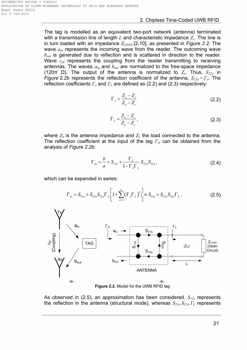
the reflection in the load. Assuming that the RFID reader transmits a pulse p(t) and defining τL = 2L/v as the round-trip propagation delay along the transmission line (v is the propagation velocity in the transmission line), a physical interpretation of (2.5) can be obtained from the bounce diagram shown in Figure 2.3. It is a two-dimensional representation of the transient waves bouncing back and forth on the tag. Zigzagging lines indicate the progress of the wave as a function of position and time. The direction of travel is from bottom to top. The terms within the series in (2.5) represent the multiple reflections of the waves between the load ZLOAD and the antenna, which appear every time delay nτL (for n = 1, 2, 3...). τp is the round-trip time delay between the tag and the reader, and τA is the delay introduced by the antenna itself. For a well-matched antenna only the first term is considered because the others vanish rapidly. Since delay information in this term is the key parameter, the best method to obtain the maximum amplitude is to make ZLOAD = ∞ or ZLOAD = 0
(open-circuit or short-circuit load, respectively), and then, design a line with Zc matched to the antenna input impedance Za. Assuming a low-loss line, the reflection coefficient ΓL is:
22 2 / Lj fj f L v
L LOAD LOADe e , (2.6)
where f is the operating frequency and ΓLOAD is the reflection coefficient of the load connected at the end of the transmission line (e. g., ΓLOAD = 1 when
ZLOAD = ∞). It can also be seen that the phase of ΓL, , directly depends
on the frequency and increases with the length L. This shows that the load reflection coefficient phase, and therefore the scattered tag (antenna) mode field Eam
(ZL) depends on the length of the transmission line. By applying the inverse Fourier transform to (2.5), we can obtain the time-domain backscattered field or, equivalently, the time-domain reflection coefficient between the incoming and outcoming waves:
1
11 12 21( ) ( ) ( )* ( )* 2 *in a a a L A LOADt S t S t S t t , (2.7)
where * denotes the convolution operator. When ΓLOAD is real (i.e. resistive or open/short-circuited loads), (2.7) can be expressed as:
11( ) ( ) 2in a LOAD L At S t g t , (2.8)
where g(t) is defined as the inverse Fourier transform of S12aS21a:
1
12 21 12 21( ) ( ) ( ) ( )* ( )a a a ag t S f S f S t S t . (2.9)
Since the structural mode S11a(t) and g(t) have a finite time duration, the time responses associated to the structural mode and the tag mode g(t-τL) can be separated if the line length L is conveniently designed. The received signal at the reader in frequency domain is then given by:
2 2 /j f L ve
UNIVERSITAT ROVIRA I VIRGILI APPLICATION OF ULTRA-WIDEBAND TECHNOLOGY TO RFID AND WIRELESS SENSORS Ángel Ramos Félix DL: T 769-2015

2. Chipless Time-Coded UWB RFID
23
1 2( ) ( , ) ( ) ( , ) ( )free in freeS f H f r f H f r P f . (2.10)
Time
p(t)
S21a(t)
S21a(t)*p(t-L-A)*LOAD
S12a(t)
S21a(t)*S12a(t)*p(t-L-2A)*LOADS12a(t)
LOAD
...
t=p+A
t=p+2A+2L/v
t=p+2A+4L/v
STRUCTURAL MODE
TAG MODE
1st Reflection
(2L/v)
TAG MODE
2nd Reflection
(4L/v)
Antenna Transmission Line
S21a(t)*S12a(t)*p(t-L-2A)*
LOAD*S22a(t)*LOAD
S11a(t)*p(t)
S22a(t)*S21a(t)*
p(t-L-A)*LOAD*LOAD
t=p
Figure 2.3. Bounce diagram for transient waves scattered at the tag
P(f) is the Fourier transform of the transmitted pulse p(t) (which includes the response of the transmitting antenna), r1 is the distance from the reader’s transmitting antenna to the tag, and r2 is the distance from the tag to the reader’s receiving antenna. Hfree is the transfer function due to free-space propagation:
12 · /1 1
( , ) ( , ) /4 · 4 ·
j f r c
free freeH f r e h t r t r cr r
, (2.11)
where c is propagation velocity in free space (c = 3 · 10
8 m/s), r=r1+r2 and δ(t) is
the Dirac delta function. The term r/c represents the delay from the antenna, and the term 1/r represents the attenuation of a spherical wave. By applying the inverse Fourier transform to (2.10), the signal received at the reader in time domain is given by:
1 2( ) ( )* ( , )* ( , )* ( )in free frees t t h t r h t r p t , (2.12)
which can be expressed as:
UNIVERSITAT ROVIRA I VIRGILI APPLICATION OF ULTRA-WIDEBAND TECHNOLOGY TO RFID AND WIRELESS SENSORS Ángel Ramos Félix DL: T 769-2015
Application of Ultra-Wideband Technology to RFID and Wireless Sensors
24
11
11
( ) ( )* ( ) ( )* ( 2 )
· ( )* ( )* ( ) ( )* ( )* ( 2 ),
p a LOAD p L A
a L LOAD p L A
s t p t S t p t g t
S t p t t g t p t t
(2.13)
where α is the round-trip attenuation factor due to propagation in free space. Both parameters are functions of the tag-reader distance r. In (2.13), S11a(t)*p(t) is the response associated to the structural mode and g(t)*p(t) is the response associated to the tag mode. In the ideal case of an antenna with infinite bandwidth, S11a(t) and g(t) can be approximated by the Dirac delta function, δ(t). Then, time resolution only depends on the type of pulse. However, the finite time duration of structural and tag modes produce an increase of the received pulse duration and some shape distortion, reducing the time resolution. This resolution determines the minimum delay that can be coded and, at the end, the number of data bits available. It will be experimentally studied in Section 2.6.1. For each tag, the ID is coded in the time difference between the structural and tag modes:
.
2 2p p L A L AStr TagID
, (2.14)
where Str. accounts for the structural mode and Tag accounts for the tag mode. Between two tags with different ID (different lengths L), the delay introduced by the antenna 2τA is the same. Therefore, 2τA can be considered as an offset term applicable to all tags.
In real measurements, the tag response is distorted by clutter and cross-coupling between the reader’s antennas. Clutter is defined as those scattering contributions not originated at the object under test (for instance, reflections at the walls or other objects). Then, the signal received at the reader can be expressed as:
'( ) ( ) ( ) ( )c ms t s t s t s t , (2.15)
where sc(t) is coupling contribution and sm(t) is the clutter due to multipath reflections. As seen in Figure 2.3, the waves that finally return to the reader are the ones due to the structural mode and the tag (antenna) modes. The tag modes repeat themselves every time instant nL/v (where n = 2, 4, 6,…). In practice, only the first tag mode, which corresponds to the delay of 2L/v, has enough amplitude to be detected. This means that the multiple tag modes, even though they exist theoretically, do not appear, and only the structural mode and the first tag mode are visible. Nevertheless, when the tag mode is heavily amplified by an active non-chipless tag, these multiple tag modes can be detected, as it will be shown in Chapter 7.
UNIVERSITAT ROVIRA I VIRGILI APPLICATION OF ULTRA-WIDEBAND TECHNOLOGY TO RFID AND WIRELESS SENSORS Ángel Ramos Félix DL: T 769-2015
2. Chipless Time-Coded UWB RFID
25
2.3. Reader design Two techniques are used to measure the tags. These techniques differ in the stimulus signal applied to the transmitting antenna of the reader. Next, both techniques are explained in detail, comparing each other in terms of cost, accuracy and speed. 2.3.1. Frequency-step approach This approach is based on using a Vector Network Analyzer (VNA). In this particular case, it corresponds to an Agilent PNA E8364C [2.14]. The VNA is connected to a control PC with a GPIB bus, and calibrated at the antennas’ reference plane, with 0 dBm of output power and with 1601 points, between 1 and 10 GHz. The reader’s transmitting antenna (Tx) is connected to the VNA port 1. Similarly, the receiving antenna (Rx) is connected to the VNA port 2. The reader’s antennas consist of a Vivaldi antenna (a scaled version of the one in [2.15]), with a good matching over the UWB band. Figure 2.4a shows the measured |S11| parameter. When using a VNA, a sine wave is frequency stepped or continuously swept over the band of interest. The time-domain response is obtained from the inverse Fourier transform of the scattering parameter S21. The step width determines the unambiguous range. Also, attention should be paid to the inverse Fourier transform if the stimulus band is smaller than the antenna bandwidth. In this case, the side lobes in the impulse response are no longer determined by the antenna response but rather by the measurement bandwidth. These side lobes can be suppressed by windowing the data before the transformation, but doing this results in slightly reducing the range resolution (compared with using a rectangular window) [2.16]. In this case, a Hamming window has been chosen. Finally, the inverse Chirp-Z transform has been used as an alternative to the inverse Fourier transform to reduce computational time [2.17]. Figure 2.4b shows a scheme of the experimental setup using a VNA, and Figure 2.4c shows a photograph of the VNA, indicating the ports where the transmitting and receiving antennas are connected. 2.3.2. Impulse-based approach In this approach, a UWB pulse is transmitted by the reader’s transmitting antenna. In order to concentrate the energy of the stimulus in the pass band of the antenna, and therefore the UWB band, monocycles are used rather than pulses. The reflected signal at the tag s(t) can be measured by means of an oscilloscope or a fast sampler. A scheme of the impulse-based approach is shown in Figure 2.5. Three commercial IR-UWB radars from different manufacturers (Geozondas, Novelda and Time Domain) are proposed as readers, and their specifications are depicted in Table 2.1.
UNIVERSITAT ROVIRA I VIRGILI APPLICATION OF ULTRA-WIDEBAND TECHNOLOGY TO RFID AND WIRELESS SENSORS Ángel Ramos Félix DL: T 769-2015
Application of Ultra-Wideband Technology to RFID and Wireless Sensors
26
The radar transmits the pulse using a pulse generator. A fast sampler, which triggers the pulse generator, receives the signal backscattered at the tag. A photograph of each radar is shown in Figure 2.6. In the Geozondas radar the sampler and the pulse generator are two separated blocks and are externally connected by a trigger cable. On the contrary, the Novelda and Time Domain radars have them integrated in the same block. In the case of the Novelda radar, a monolithic integrated circuit includes the pulse generator and the sampler. In the case of the Time Domain radar, the transmitter and receiver are integrated, but the sampler is made by an external Field Programmable Gate Array (FPGA). In order to sample the received signal, the Geozondas radar uses a sampling oscilloscope, the Novelda radar uses a method based on a continuous time binary valued (CTBV) design paradigm [2.18], and the Time Domain radar uses a rake receiver [2.19]. The power consumption of the integrated radars is lower than the discrete one.
0 2 4 6 8 10
-30
-20
-10
0
Frequency (GHz)
|S11
| (d
B)
Top
Bottom
-a-
Inverse
Fourier
Transform
Agilent
E8364C
Network
Analyzer
Tx Antenna
(Port 1)
TAGRx Antenna
(Port 2)
GPIB
UWB
Time
Signal
Control PC
-b-
Tx Antenna
(Port 1)
Rx Antenna
(Port 2)
S21S21
-c-
Figure 2.4. (a) Simulated |S11| of the antennas used in the reader. In the inset, photographs of the antennas. (b) Scheme and (c) photograph of the frequency-step approach
Figure 2.7 shows a comparison of the pulses reflected at a large metal plate using the Vivaldi antennas from Figure 2.4a. Depending on the technique used to generate the pulse [2.20], its shape is different in time domain. Moreover, the antennas introduce a derivative effect which distorts its shape. However, as it can be seen in frequency domain, the NVA6100 and P400 pulses mostly comply with FCC regulations, since they are centered at 4.3 GHz. The pulse from the GZ1120ME-35EV generator is centered at a lower frequency and therefore a part of it falls outside the FCC mask. However, as it will be seen in
UNIVERSITAT ROVIRA I VIRGILI APPLICATION OF ULTRA-WIDEBAND TECHNOLOGY TO RFID AND WIRELESS SENSORS Ángel Ramos Félix DL: T 769-2015
2. Chipless Time-Coded UWB RFID
27
Section 3.2.2, it can be used for certain sensing applications where the sensor performance is limited in frequency.
Radar Resolution (ps/point)
Maximum Required
Power
Number of Points
Time Window
(ns)
Central Freq. (GHz)
Measured Bandwidth*
(GHz)
Samp. Method
Novelda NVA6100 (R640 Dev. Kit)
[2.6] 30 120 mW 512 15.36 4.35 1.5 CTBV
Geozondas GZ6E (Sampler) + GZ1120ME-35EV (Pulse Generator)
[2.5]
25 15.6 W
(1.3 A @ 12 V)
4096 20 3.5 1.9 Sampling Oscillosc.
Time Domain PulsON P400
MRM [2.7]
61 6.90 W 480 29.28 4.3 1.1 Rake
*Approximated, at -3 dB from maximum amplitude (see Figure 2.7b)
Table 2.1. Specifications of the commercial radars proposed for the impulse-based approach
USB / Trig
ge
rTx Antenna
TAG
Rx Antenna
UWB
Time
Signal
Control PC
Ethernet
Radar
Pulse
Generator
Sampler
Figure 2.5. Scheme of the impulse-based approach
2.3.3. Comparison and conclusions The advantages of the step-frequency approach are its excellent drift stability and random noise suppression because of the narrowband receivers, as well as its flexibility in the choice of the stimulus band. It is, however, the most expensive and slowest method. The step-frequency approach also requires more computational power since it needs to apply the inverse Fourier transform each time a measurement is done. Thus, the measurement time of a VNA is several times larger than a IR-UWB radar and its power consumption is also greater than that of a radar. The step-frequency approach is although, a good method to take as reference. The impulse-based approach, specially with integrated radars, provides a potentially low-cost, fast acquisition and portable solution. There are also commercial radar ICs which can be used to build fully custom readers [2.21]. However, the resolution is limited, as well as the stability both in amplitude (offset) and time (jitter). In addition, the large bandwidth of the impulse-based approach reduces the signal-to-noise ratio of the system. Table 2.2 summarizes the main differences between both approaches.
UNIVERSITAT ROVIRA I VIRGILI APPLICATION OF ULTRA-WIDEBAND TECHNOLOGY TO RFID AND WIRELESS SENSORS Ángel Ramos Félix DL: T 769-2015
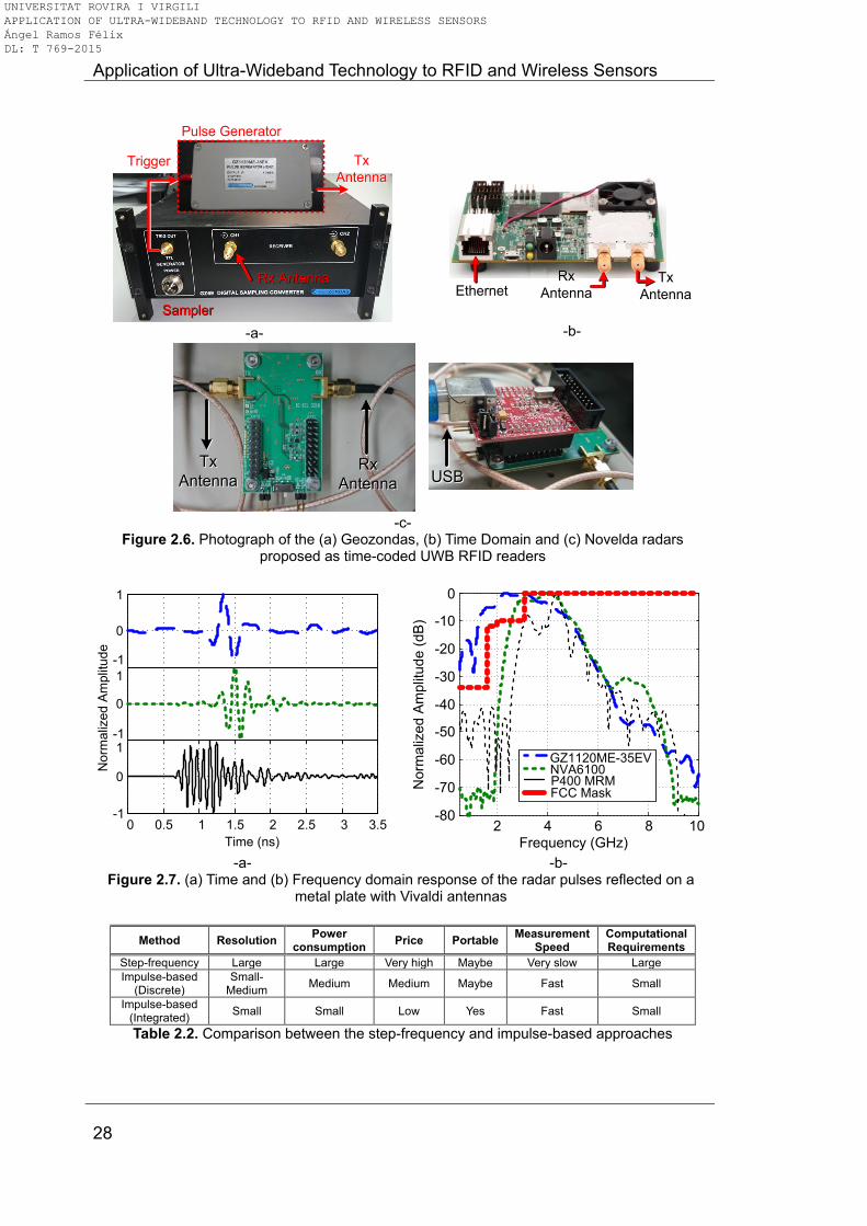
Application of Ultra-Wideband Technology to RFID and Wireless Sensors
28
TriggerTrigger Tx
Antenna
Tx
Antenna
Rx AntennaRx Antenna
Pulse GeneratorPulse Generator
SamplerSampler
-a-
Rx
Antenna
Rx
AntennaTx
Antenna
Tx
AntennaEthernetEthernet
-b-
Tx
Antenna
Tx
AntennaRx
Antenna
Rx
Antenna USBUSB
-c-
Figure 2.6. Photograph of the (a) Geozondas, (b) Time Domain and (c) Novelda radars proposed as time-coded UWB RFID readers
-1
0
1
-1
0
1
0 0.5 1 1.5 2 2.5 3 3.5-1
0
1
Time (ns)
Norm
aliz
ed A
mplit
ude
2 4 6 8 10-80
-70
-60
-50
-40
-30
-20
-10
0
Frequency (GHz)
Norm
aliz
ed A
mplit
ude (
dB
)
GZ1120ME-35EVNVA6100P400 MRMFCC Mask
-a- -b-
Figure 2.7. (a) Time and (b) Frequency domain response of the radar pulses reflected on a metal plate with Vivaldi antennas
Method Resolution Power
consumption Price Portable
Measurement Speed
Computational Requirements
Step-frequency Large Large Very high Maybe Very slow Large
Impulse-based (Discrete)
Small-Medium
Medium Medium Maybe Fast Small
Impulse-based (Integrated)
Small Small Low Yes Fast Small
Table 2.2. Comparison between the step-frequency and impulse-based approaches
UNIVERSITAT ROVIRA I VIRGILI APPLICATION OF ULTRA-WIDEBAND TECHNOLOGY TO RFID AND WIRELESS SENSORS Ángel Ramos Félix DL: T 769-2015
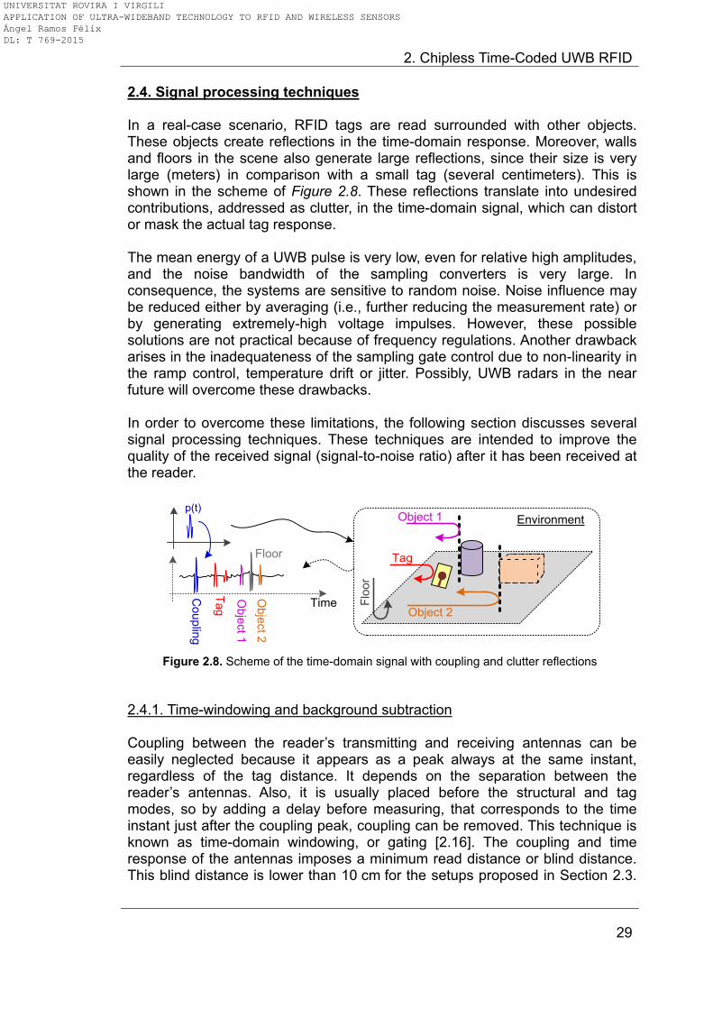
2. Chipless Time-Coded UWB RFID
29
2.4. Signal processing techniques In a real-case scenario, RFID tags are read surrounded with other objects. These objects create reflections in the time-domain response. Moreover, walls and floors in the scene also generate large reflections, since their size is very large (meters) in comparison with a small tag (several centimeters). This is shown in the scheme of Figure 2.8. These reflections translate into undesired contributions, addressed as clutter, in the time-domain signal, which can distort or mask the actual tag response. The mean energy of a UWB pulse is very low, even for relative high amplitudes, and the noise bandwidth of the sampling converters is very large. In consequence, the systems are sensitive to random noise. Noise influence may be reduced either by averaging (i.e., further reducing the measurement rate) or by generating extremely-high voltage impulses. However, these possible solutions are not practical because of frequency regulations. Another drawback arises in the inadequateness of the sampling gate control due to non-linearity in the ramp control, temperature drift or jitter. Possibly, UWB radars in the near future will overcome these drawbacks. In order to overcome these limitations, the following section discusses several signal processing techniques. These techniques are intended to improve the quality of the received signal (signal-to-noise ratio) after it has been received at the reader.
Object 2
Object 1
Time
Co
up
ling
Ob
ject 1
Ob
ject 2
p(t)
Floor
Ta
g
Tag
Flo
or
Environment
Figure 2.8. Scheme of the time-domain signal with coupling and clutter reflections
2.4.1. Time-windowing and background subtraction Coupling between the reader’s transmitting and receiving antennas can be easily neglected because it appears as a peak always at the same instant, regardless of the tag distance. It depends on the separation between the reader’s antennas. Also, it is usually placed before the structural and tag modes, so by adding a delay before measuring, that corresponds to the time instant just after the coupling peak, coupling can be removed. This technique is known as time-domain windowing, or gating [2.16]. The coupling and time response of the antennas imposes a minimum read distance or blind distance. This blind distance is lower than 10 cm for the setups proposed in Section 2.3.
UNIVERSITAT ROVIRA I VIRGILI APPLICATION OF ULTRA-WIDEBAND TECHNOLOGY TO RFID AND WIRELESS SENSORS Ángel Ramos Félix DL: T 769-2015
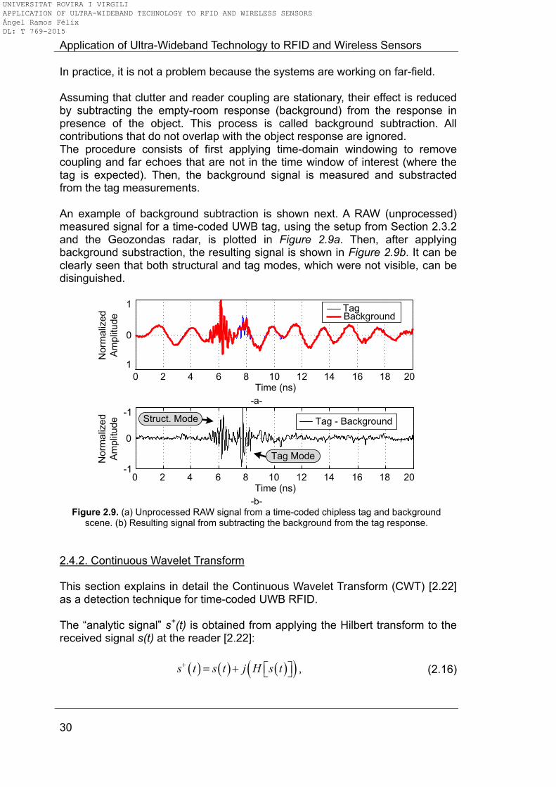
Application of Ultra-Wideband Technology to RFID and Wireless Sensors
30
In practice, it is not a problem because the systems are working on far-field. Assuming that clutter and reader coupling are stationary, their effect is reduced by subtracting the empty-room response (background) from the response in presence of the object. This process is called background subtraction. All contributions that do not overlap with the object response are ignored. The procedure consists of first applying time-domain windowing to remove coupling and far echoes that are not in the time window of interest (where the tag is expected). Then, the background signal is measured and substracted from the tag measurements.
An example of background subtraction is shown next. A RAW (unprocessed) measured signal for a time-coded UWB tag, using the setup from Section 2.3.2 and the Geozondas radar, is plotted in Figure 2.9a. Then, after applying background substraction, the resulting signal is shown in Figure 2.9b. It can be clearly seen that both structural and tag modes, which were not visible, can be disinguished.
0
1
No
rma
lize
d
Am
plit
ud
e
1
0 2 4 6 8 10 12 14 16 18 20Time (ns)
TagBackground
-a-
-1
0 2 4 6 8 10 12 14 16 18 20-1
0
Time (ns)
Struct. Mode
Tag Mode
Tag - Background
Norm
aliz
ed
Am
plit
ude
-b-
Figure 2.9. (a) Unprocessed RAW signal from a time-coded chipless tag and background scene. (b) Resulting signal from subtracting the background from the tag response.
2.4.2. Continuous Wavelet Transform This section explains in detail the Continuous Wavelet Transform (CWT) [2.22] as a detection technique for time-coded UWB RFID. The “analytic signal” s+(t) is obtained from applying the Hilbert transform to the received signal s(t) at the reader [2.22]:
s t s t j H s t , (2.16)
UNIVERSITAT ROVIRA I VIRGILI APPLICATION OF ULTRA-WIDEBAND TECHNOLOGY TO RFID AND WIRELESS SENSORS Ángel Ramos Félix DL: T 769-2015
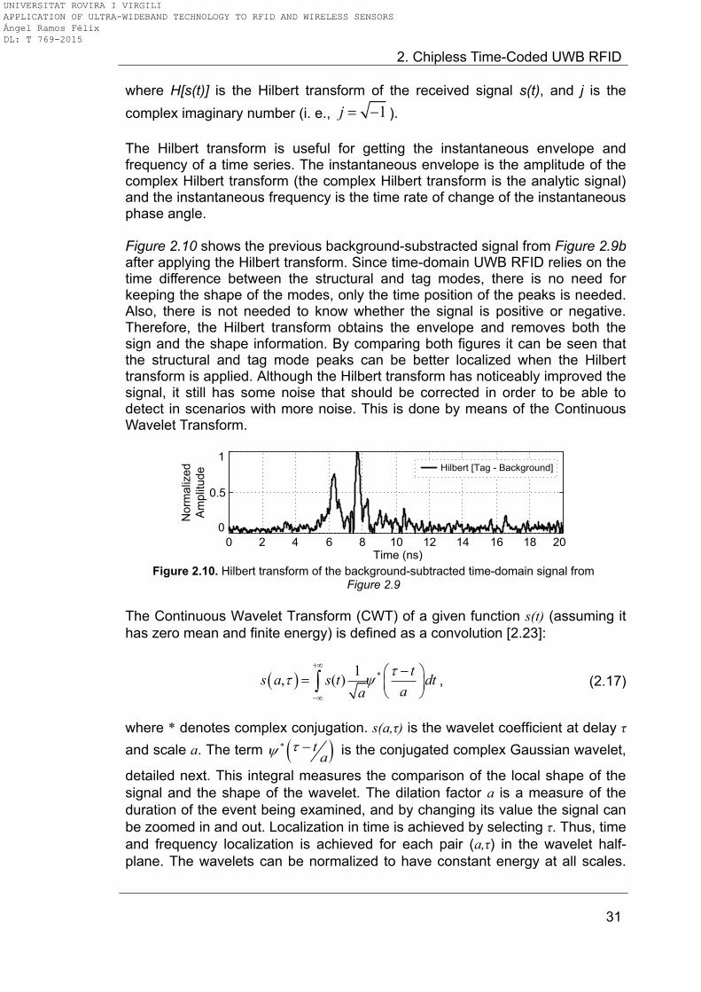
2. Chipless Time-Coded UWB RFID
31
where H[s(t)] is the Hilbert transform of the received signal s(t), and j is the
complex imaginary number (i. e., 1j ).
The Hilbert transform is useful for getting the instantaneous envelope and frequency of a time series. The instantaneous envelope is the amplitude of the complex Hilbert transform (the complex Hilbert transform is the analytic signal) and the instantaneous frequency is the time rate of change of the instantaneous phase angle. Figure 2.10 shows the previous background-substracted signal from Figure 2.9b after applying the Hilbert transform. Since time-domain UWB RFID relies on the time difference between the structural and tag modes, there is no need for keeping the shape of the modes, only the time position of the peaks is needed. Also, there is not needed to know whether the signal is positive or negative. Therefore, the Hilbert transform obtains the envelope and removes both the sign and the shape information. By comparing both figures it can be seen that the structural and tag mode peaks can be better localized when the Hilbert transform is applied. Although the Hilbert transform has noticeably improved the signal, it still has some noise that should be corrected in order to be able to detect in scenarios with more noise. This is done by means of the Continuous Wavelet Transform.
Norm
aliz
ed
Am
plit
ude
0 2 4 6 8 10 12 14 16 18 20Time (ns)
0
0.5
1
Hilbert [Tag - Background]
Figure 2.10. Hilbert transform of the background-subtracted time-domain signal from
Figure 2.9
The Continuous Wavelet Transform (CWT) of a given function s(t) (assuming it
has zero mean and finite energy) is defined as a convolution [2.23]:
*1, ( )
ts a s t dt
aa
, (2.17)
where * denotes complex conjugation. s(a,τ) is the wavelet coefficient at delay τ
and scale a. The term * ta
is the conjugated complex Gaussian wavelet,
detailed next. This integral measures the comparison of the local shape of the
signal and the shape of the wavelet. The dilation factor a is a measure of the
duration of the event being examined, and by changing its value the signal can
be zoomed in and out. Localization in time is achieved by selecting τ. Thus, time
and frequency localization is achieved for each pair (a,τ) in the wavelet half-
plane. The wavelets can be normalized to have constant energy at all scales.
UNIVERSITAT ROVIRA I VIRGILI APPLICATION OF ULTRA-WIDEBAND TECHNOLOGY TO RFID AND WIRELESS SENSORS Ángel Ramos Félix DL: T 769-2015
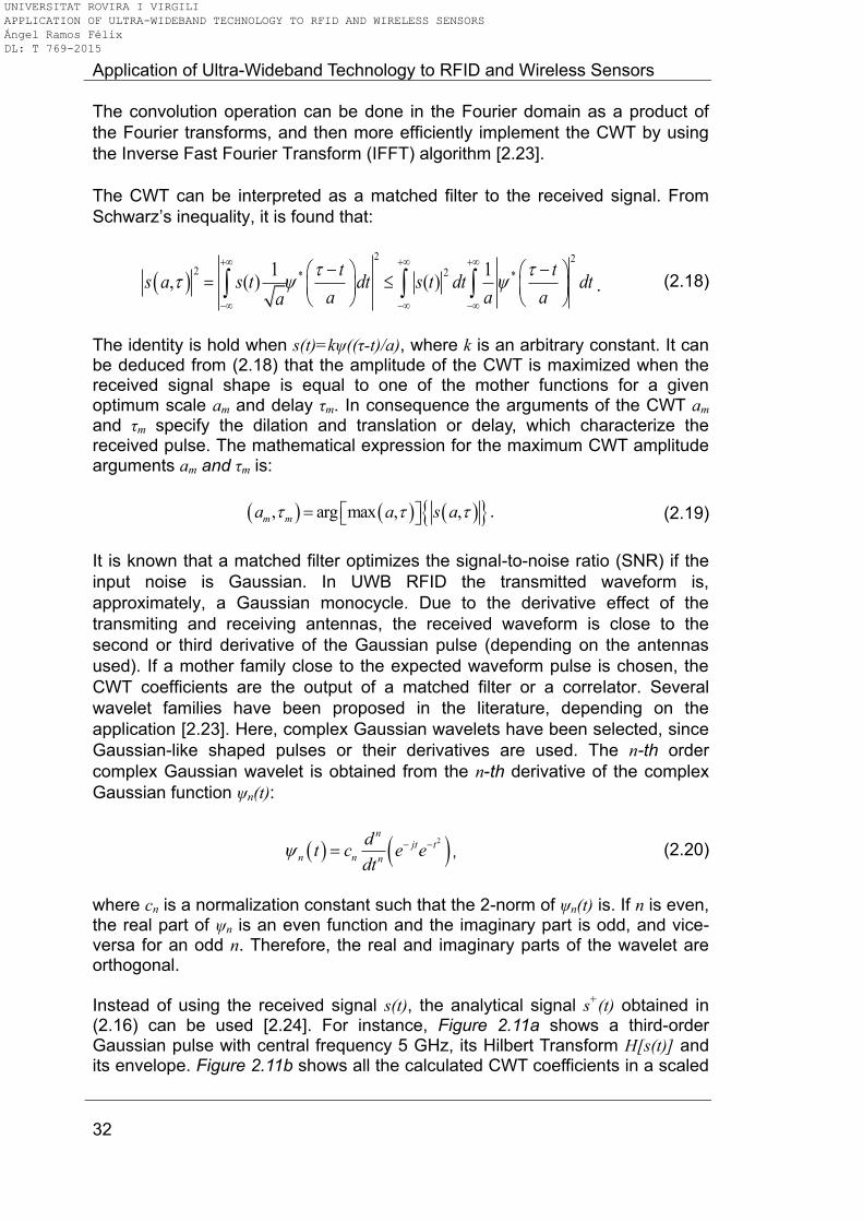
Application of Ultra-Wideband Technology to RFID and Wireless Sensors
32
The convolution operation can be done in the Fourier domain as a product of
the Fourier transforms, and then more efficiently implement the CWT by using
the Inverse Fast Fourier Transform (IFFT) algorithm [2.23].
The CWT can be interpreted as a matched filter to the received signal. From
Schwarz’s inequality, it is found that:
2 22 2* *1 1
, ( ) ( )t t
s a s t dt s t dt dta a aa
. (2.18)
The identity is hold when s(t)=kψ((τ-t)/a), where k is an arbitrary constant. It can be deduced from (2.18) that the amplitude of the CWT is maximized when the received signal shape is equal to one of the mother functions for a given optimum scale am and delay τm. In consequence the arguments of the CWT am and τm specify the dilation and translation or delay, which characterize the received pulse. The mathematical expression for the maximum CWT amplitude arguments am and τm is:
, arg max , ,m ma a s a . (2.19)
It is known that a matched filter optimizes the signal-to-noise ratio (SNR) if the
input noise is Gaussian. In UWB RFID the transmitted waveform is,
approximately, a Gaussian monocycle. Due to the derivative effect of the
transmiting and receiving antennas, the received waveform is close to the
second or third derivative of the Gaussian pulse (depending on the antennas
used). If a mother family close to the expected waveform pulse is chosen, the
CWT coefficients are the output of a matched filter or a correlator. Several
wavelet families have been proposed in the literature, depending on the
application [2.23]. Here, complex Gaussian wavelets have been selected, since
Gaussian-like shaped pulses or their derivatives are used. The n-th order
complex Gaussian wavelet is obtained from the n-th derivative of the complex
Gaussian function ψn(t):
2
njt t
n n n
dt c e e
dt , (2.20)
where cn is a normalization constant such that the 2-norm of ψn(t) is. If n is even, the real part of ψn is an even function and the imaginary part is odd, and vice-versa for an odd n. Therefore, the real and imaginary parts of the wavelet are orthogonal. Instead of using the received signal s(t), the analytical signal s
+(t) obtained in
(2.16) can be used [2.24]. For instance, Figure 2.11a shows a third-order Gaussian pulse with central frequency 5 GHz, its Hilbert Transform H[s(t)] and its envelope. Figure 2.11b shows all the calculated CWT coefficients in a scaled
UNIVERSITAT ROVIRA I VIRGILI APPLICATION OF ULTRA-WIDEBAND TECHNOLOGY TO RFID AND WIRELESS SENSORS Ángel Ramos Félix DL: T 769-2015
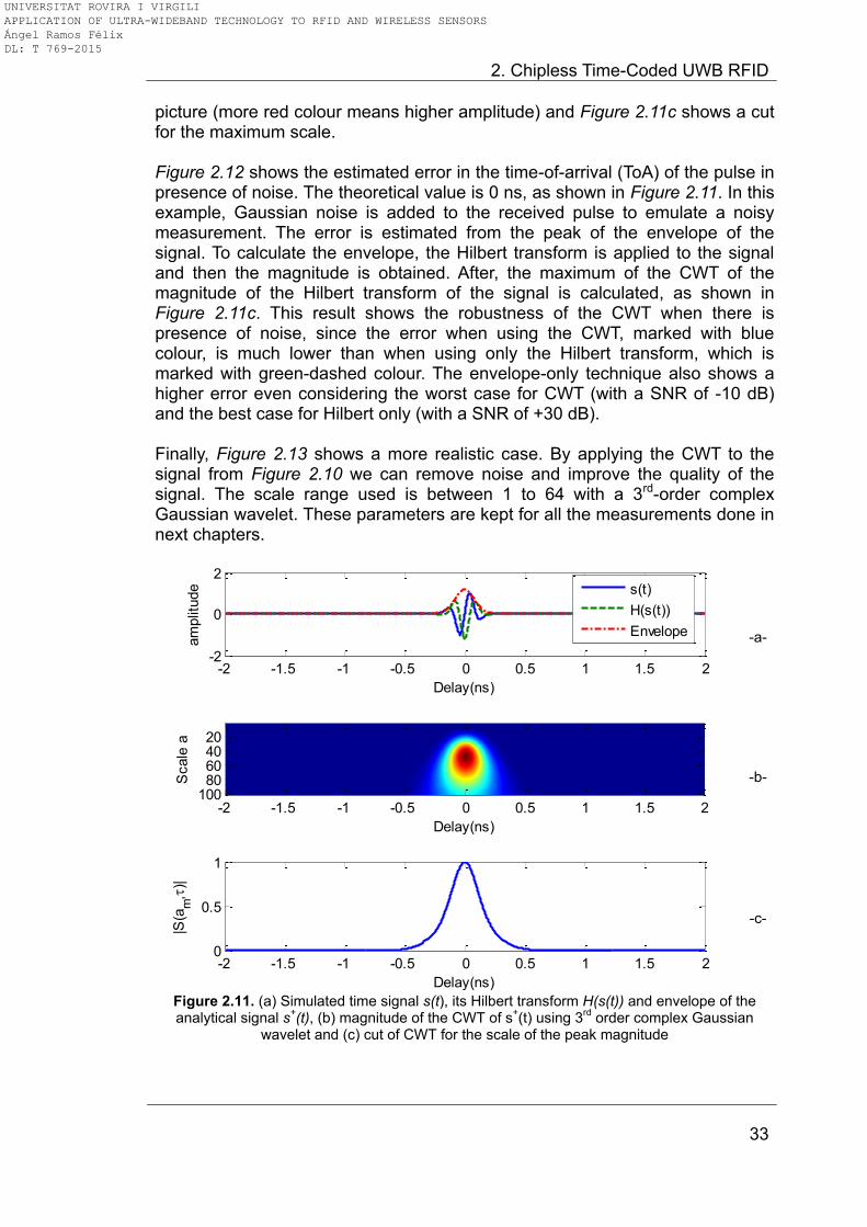
2. Chipless Time-Coded UWB RFID
33
picture (more red colour means higher amplitude) and Figure 2.11c shows a cut for the maximum scale.
Figure 2.12 shows the estimated error in the time-of-arrival (ToA) of the pulse in presence of noise. The theoretical value is 0 ns, as shown in Figure 2.11. In this example, Gaussian noise is added to the received pulse to emulate a noisy measurement. The error is estimated from the peak of the envelope of the signal. To calculate the envelope, the Hilbert transform is applied to the signal and then the magnitude is obtained. After, the maximum of the CWT of the magnitude of the Hilbert transform of the signal is calculated, as shown in Figure 2.11c. This result shows the robustness of the CWT when there is presence of noise, since the error when using the CWT, marked with blue colour, is much lower than when using only the Hilbert transform, which is marked with green-dashed colour. The envelope-only technique also shows a higher error even considering the worst case for CWT (with a SNR of -10 dB) and the best case for Hilbert only (with a SNR of +30 dB). Finally, Figure 2.13 shows a more realistic case. By applying the CWT to the signal from Figure 2.10 we can remove noise and improve the quality of the signal. The scale range used is between 1 to 64 with a 3rd-order complex Gaussian wavelet. These parameters are kept for all the measurements done in next chapters.
-a-
-b-
-c-
Figure 2.11. (a) Simulated time signal s(t), its Hilbert transform H(s(t)) and envelope of the analytical signal s
+(t), (b) magnitude of the CWT of s
+(t) using 3
rd order complex Gaussian
wavelet and (c) cut of CWT for the scale of the peak magnitude
-2 -1.5 -1 -0.5 0 0.5 1 1.5 2-2
0
2
Delay(ns)
am
plit
ude
Delay(ns)
Scale
a
-2 -1.5 -1 -0.5 0 0.5 1 1.5 2
20406080
100
-2 -1.5 -1 -0.5 0 0.5 1 1.5 20
0.5
1
Delay(ns)
|S(a
m,
)|
s(t)
H(s(t))
Envelope
UNIVERSITAT ROVIRA I VIRGILI APPLICATION OF ULTRA-WIDEBAND TECHNOLOGY TO RFID AND WIRELESS SENSORS Ángel Ramos Félix DL: T 769-2015
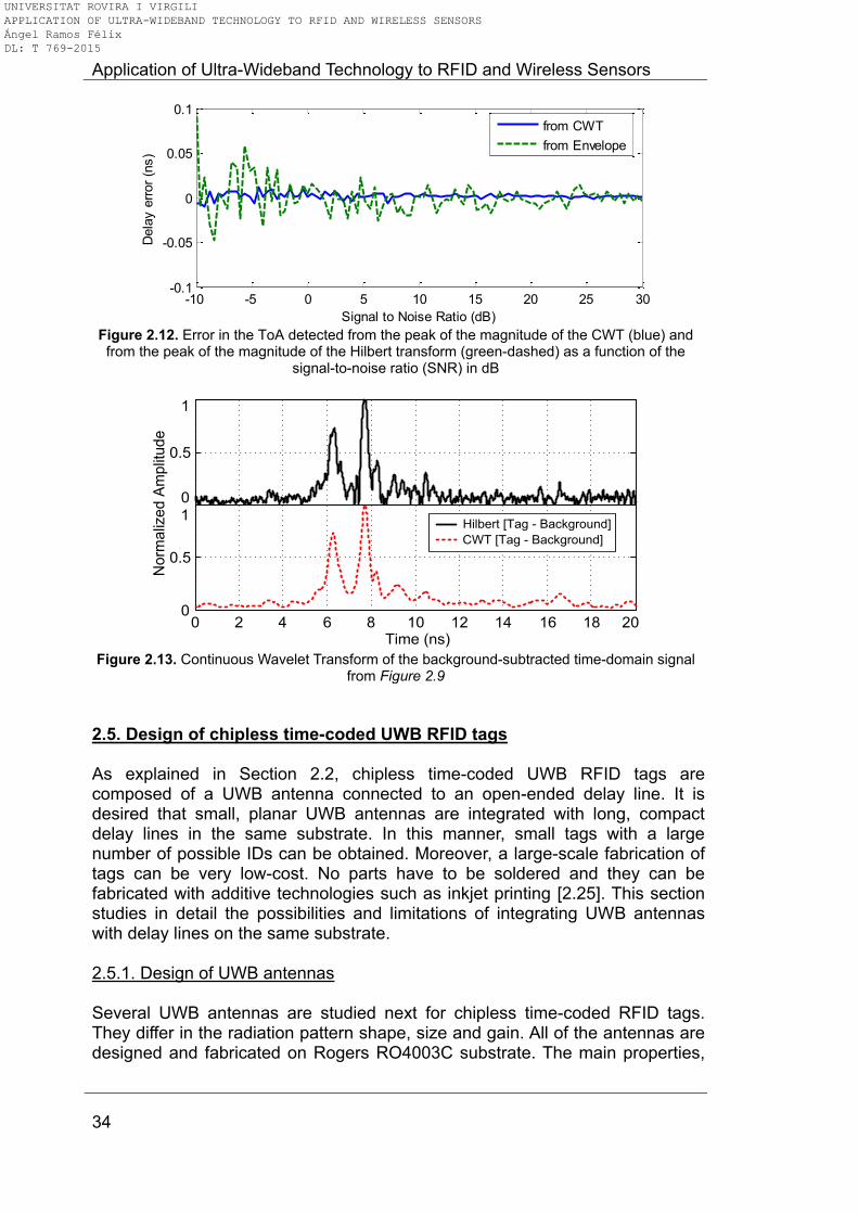
Application of Ultra-Wideband Technology to RFID and Wireless Sensors
34
Figure 2.12. Error in the ToA detected from the peak of the magnitude of the CWT (blue) and from the peak of the magnitude of the Hilbert transform (green-dashed) as a function of the
signal-to-noise ratio (SNR) in dB
No
rma
lize
d A
mp
litu
de
0 2 4 6 8 10 12 14 16 18 20Time (ns)
0
0.5
1
0
0.5
1
Hilbert [Tag - Background]
CWT [Tag - Background]
Figure 2.13. Continuous Wavelet Transform of the background-subtracted time-domain signal
from Figure 2.9
2.5. Design of chipless time-coded UWB RFID tags As explained in Section 2.2, chipless time-coded UWB RFID tags are composed of a UWB antenna connected to an open-ended delay line. It is desired that small, planar UWB antennas are integrated with long, compact delay lines in the same substrate. In this manner, small tags with a large number of possible IDs can be obtained. Moreover, a large-scale fabrication of tags can be very low-cost. No parts have to be soldered and they can be fabricated with additive technologies such as inkjet printing [2.25]. This section studies in detail the possibilities and limitations of integrating UWB antennas with delay lines on the same substrate. 2.5.1. Design of UWB antennas Several UWB antennas are studied next for chipless time-coded RFID tags. They differ in the radiation pattern shape, size and gain. All of the antennas are designed and fabricated on Rogers RO4003C substrate. The main properties,
-10 -5 0 5 10 15 20 25 30-0.1
-0.05
0
0.05
0.1
Signal to Noise Ratio (dB)
Dela
y e
rror
(ns)
from CWT
from Envelope
UNIVERSITAT ROVIRA I VIRGILI APPLICATION OF ULTRA-WIDEBAND TECHNOLOGY TO RFID AND WIRELESS SENSORS Ángel Ramos Félix DL: T 769-2015
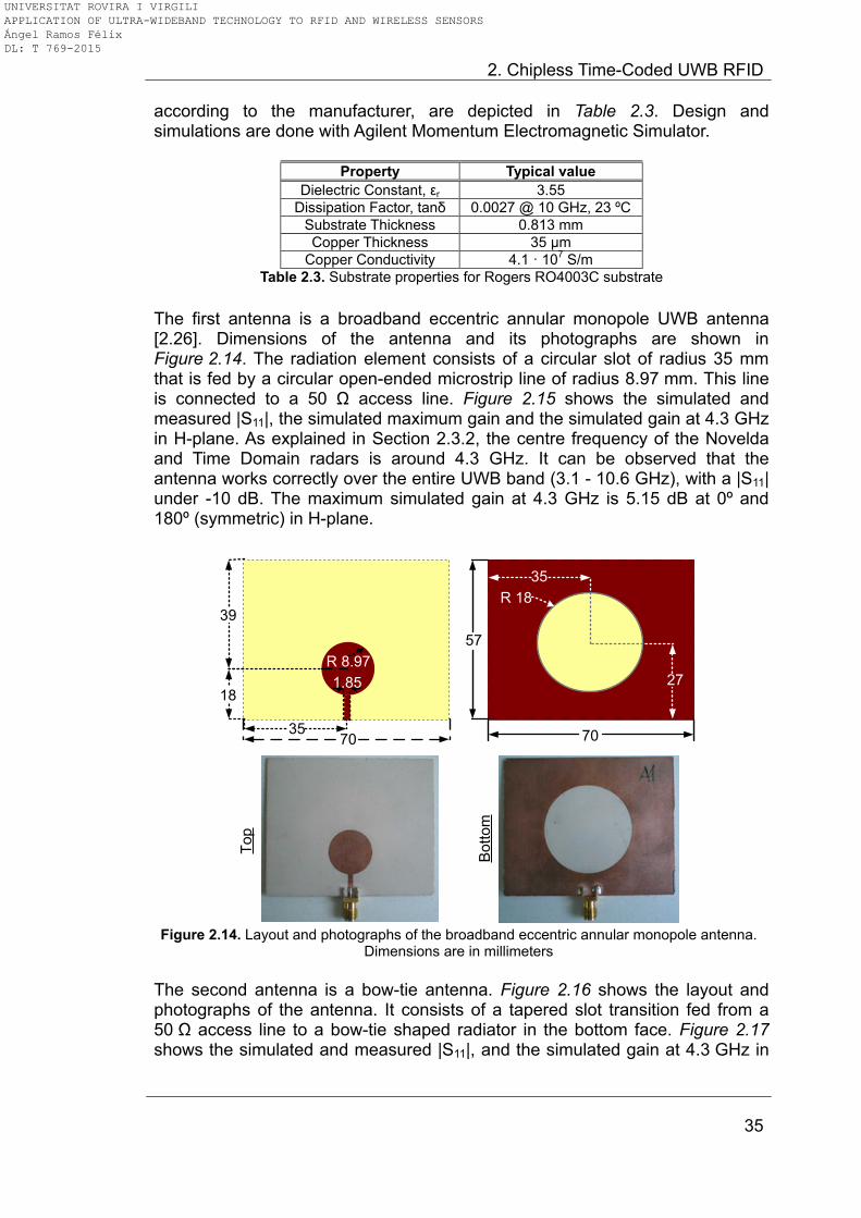
2. Chipless Time-Coded UWB RFID
35
according to the manufacturer, are depicted in Table 2.3. Design and simulations are done with Agilent Momentum Electromagnetic Simulator.
Property Typical value
Dielectric Constant, εr 3.55
Dissipation Factor, tanδ 0.0027 @ 10 GHz, 23 ºC
Substrate Thickness 0.813 mm
Copper Thickness 35 μm
Copper Conductivity 4.1 · 107 S/m
Table 2.3. Substrate properties for Rogers RO4003C substrate
The first antenna is a broadband eccentric annular monopole UWB antenna [2.26]. Dimensions of the antenna and its photographs are shown in Figure 2.14. The radiation element consists of a circular slot of radius 35 mm that is fed by a circular open-ended microstrip line of radius 8.97 mm. This line is connected to a 50 Ω access line. Figure 2.15 shows the simulated and measured |S11|, the simulated maximum gain and the simulated gain at 4.3 GHz in H-plane. As explained in Section 2.3.2, the centre frequency of the Novelda and Time Domain radars is around 4.3 GHz. It can be observed that the antenna works correctly over the entire UWB band (3.1 - 10.6 GHz), with a |S11| under -10 dB. The maximum simulated gain at 4.3 GHz is 5.15 dB at 0º and 180º (symmetric) in H-plane.
7035
39
1.85
R 8.97
27
35
57
70
R 18
18
Top
Bottom
Figure 2.14. Layout and photographs of the broadband eccentric annular monopole antenna.
Dimensions are in millimeters
The second antenna is a bow-tie antenna. Figure 2.16 shows the layout and photographs of the antenna. It consists of a tapered slot transition fed from a 50 Ω access line to a bow-tie shaped radiator in the bottom face. Figure 2.17 shows the simulated and measured |S11|, and the simulated gain at 4.3 GHz in
UNIVERSITAT ROVIRA I VIRGILI APPLICATION OF ULTRA-WIDEBAND TECHNOLOGY TO RFID AND WIRELESS SENSORS Ángel Ramos Félix DL: T 769-2015

Application of Ultra-Wideband Technology to RFID and Wireless Sensors
36
the H-plane. Again, a good agreement is observed, with a maximum gain of 2.97 dB at 0º and 180º (symmetric).
-80
-60
-40-20
010 dB
90o
60o
30o0o
-30 o
-60o
-90o
-120o
-150 o180o
150o
120 o
2 4 6 8 10 12-50
-40
-30
-20
-10
0
10
Frequency (GHz)
|S11
| (d
B)
MeasuredSimulatedSimulated Gain
Angle (Deg)
Gain
(dB
)-a- -b-
Figure 2.15. (a) Simulated and measured |S11|, and simulated maximum gain of the broadband eccentric annular monopole antenna. (b) Simulated gain at 4.3 GHz in H-plane
0.5
1.85
0.5
R 8.1, 90º
R2
6.0
7,
60
º
Top
Bottom
45
.50
22.2
5
353570
Figure 2.16. Layout and photographs of the bow-tie antenna. Dimensions are in millimeters
The third antenna is a dipole antenna. Its layout is shown in the inset of Figure 2.18. It is composed of two ellipses and an access line. As shown in the simulations from Figure 2.18, the antenna is well-matched for frequencies above 1.2 GHz. The maximum gain is achieved at -111º, with 3.12 dB. Finally, the last antenna studied is a Vivaldi antenna. Figure 2.19 shows the layout of the antenna with its dimensions. It consists of a tapered slot transition with an exponential taper radiator on the bottom face. Figure 2.20 shows the simulated |S11| and the simulated gain in H-plane at 4.3 GHz. A good matching for frequencies above 1.5 GHz is observed. In this case, the shape of the radiation pattern is noticeably different from the other antennas, with a maximum radiation lobe at 68º. The maximum gain at this angle is 6.52 dB, which is larger than in the other designs.
UNIVERSITAT ROVIRA I VIRGILI APPLICATION OF ULTRA-WIDEBAND TECHNOLOGY TO RFID AND WIRELESS SENSORS Ángel Ramos Félix DL: T 769-2015
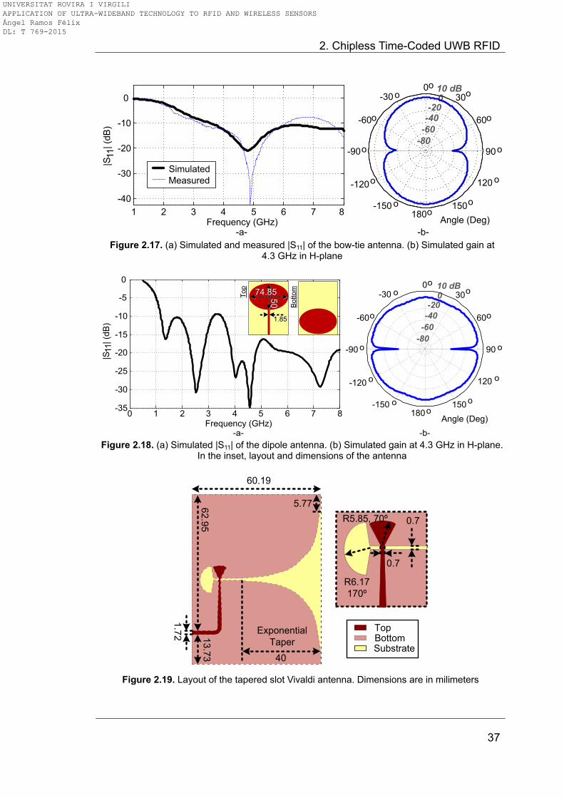
2. Chipless Time-Coded UWB RFID
37
-80
-60
-40-20
010 dB
90o
60o
30o0o
-30 o
-60o
-90o
-120o
-150 o180o
150o
120 o
Angle (Deg)1 2 3 4 5 6 7 8
-40
-30
-20
-10
0
Frequency (GHz)
|S11
| (d
B)
Simulated
Measured
-a- -b- Figure 2.17. (a) Simulated and measured |S11| of the bow-tie antenna. (b) Simulated gain at
4.3 GHz in H-plane
0 1 2 3 4 5 6 7 8-35
-30
-25
-20
-15
-10
-5
0
Frequency (GHz)
|S11
| (d
B)
74.8574.855
05
0
1.851.85
-80
-60
-40
-20010 dB
90 o
60o
30o
0o
-30 o
-60o
-90 o
-120 o
-150 o
180o150 o
120 o
Angle (Deg)
Top
Bottom
-a- -b- Figure 2.18. (a) Simulated |S11| of the dipole antenna. (b) Simulated gain at 4.3 GHz in H-plane.
In the inset, layout and dimensions of the antenna
13.7
362
.95
60.19
1.7
2
40
5.77
R6.17
170º
R5.85, 70º 0.7
0.7
TopBottomSubstrate
Exponential
Taper
Figure 2.19. Layout of the tapered slot Vivaldi antenna. Dimensions are in milimeters
UNIVERSITAT ROVIRA I VIRGILI APPLICATION OF ULTRA-WIDEBAND TECHNOLOGY TO RFID AND WIRELESS SENSORS Ángel Ramos Félix DL: T 769-2015
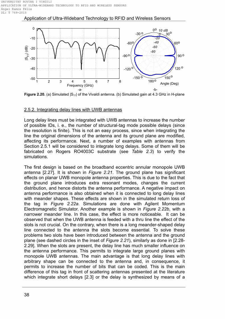
Application of Ultra-Wideband Technology to RFID and Wireless Sensors
38
1 2 3 4 5 6 7 8Frequency (GHz)
-80
-60
-40
-20010 dB
90 o
60o
30o
0o
-30 o
-60o
-90 o
-120 o
-150 o
180o150 o
120 o
Angle (Deg)
-50
-40
-30
-20
-10
0|S
11| (d
B)
-a- -b- Figure 2.20. (a) Simulated |S11| of the Vivaldi antenna. (b) Simulated gain at 4.3 GHz in H-plane
2.5.2. Integrating delay lines with UWB antennas Long delay lines must be integrated with UWB antennas to increase the number of possible IDs, i. e., the number of structural-tag mode possible delays (since the resolution is finite). This is not an easy process, since when integrating the line the original dimensions of the antenna and its ground plane are modified, affecting its performance. Next, a number of examples with antennas from Section 2.5.1 will be considered to integrate long delays. Some of them will be fabricated on Rogers RO4003C substrate (see Table 2.3) to verify the simulations. The first design is based on the broadband eccentric annular monopole UWB antenna [2.27]. It is shown in Figure 2.21. The ground plane has significant effects on planar UWB monopole antenna properties. This is due to the fact that the ground plane introduces extra resonant modes, changes the current distribution, and hence distorts the antenna performance. A negative impact on antenna performance is also obtained when it is connected to long delay lines with meander shapes. These effects are shown in the simulated return loss of the tag in Figure 2.22a. Simulations are done with Agilent Momentum Electromagnetic Simulator. Another example is shown in Figure 2.22b, with a narrower meander line. In this case, the effect is more noticeable. It can be observed that when the UWB antenna is feeded with a thru line the effect of the slots is not crucial. On the contrary, when there is a long meander-shaped delay line connected to the antenna the slots become essential. To solve these problems two slots have been introduced between the antenna and the ground plane (see dashed circles in the inset of Figure 2.21), similarly as done in [2.28-2.29]. When the slots are present, the delay line has much smaller influence on the antenna performance. This permits to integrate large ground planes with monopole UWB antennas. The main advantage is that long delay lines with arbitrary shape can be connected to the antenna and, in consequence, it permits to increase the number of bits that can be coded. This is the main difference of this tag in front of scattering antennas presented at the literature which integrate short delays [2.3] or the delay is synthesized by means of a
UNIVERSITAT ROVIRA I VIRGILI APPLICATION OF ULTRA-WIDEBAND TECHNOLOGY TO RFID AND WIRELESS SENSORS Ángel Ramos Félix DL: T 769-2015
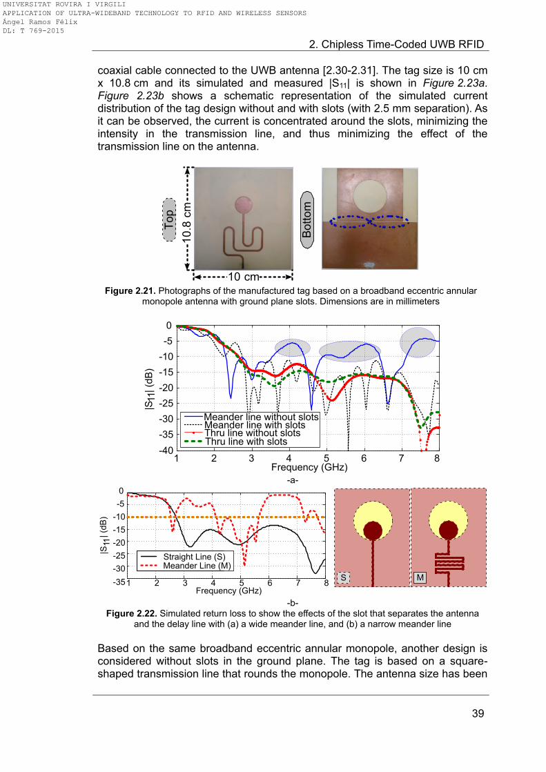
2. Chipless Time-Coded UWB RFID
39
coaxial cable connected to the UWB antenna [2.30-2.31]. The tag size is 10 cm x 10.8 cm and its simulated and measured |S11| is shown in Figure 2.23a. Figure 2.23b shows a schematic representation of the simulated current distribution of the tag design without and with slots (with 2.5 mm separation). As it can be observed, the current is concentrated around the slots, minimizing the intensity in the transmission line, and thus minimizing the effect of the transmission line on the antenna.
10
.8cm
10 cm
Top
Bottom
Figure 2.21. Photographs of the manufactured tag based on a broadband eccentric annular
monopole antenna with ground plane slots. Dimensions are in millimeters
1 2 3 4 5 6 7 8-40
-35
-30
-25
-20
-15
-10
-5
0
Frequency (GHz)
|S11
| (d
B)
Meander line without slotsMeander line with slotsThru line without slotsThru line with slots
-a-
1 2 3 4 5 6 7 8-35
-30
-25
-20
-15
-10
-5
0
Frequency (GHz)
|S11
| (
dB
)
Straight Line (S)Meander Line (M)
S M
-b- Figure 2.22. Simulated return loss to show the effects of the slot that separates the antenna
and the delay line with (a) a wide meander line, and (b) a narrow meander line
Based on the same broadband eccentric annular monopole, another design is considered without slots in the ground plane. The tag is based on a square-shaped transmission line that rounds the monopole. The antenna size has been
UNIVERSITAT ROVIRA I VIRGILI APPLICATION OF ULTRA-WIDEBAND TECHNOLOGY TO RFID AND WIRELESS SENSORS Ángel Ramos Félix DL: T 769-2015
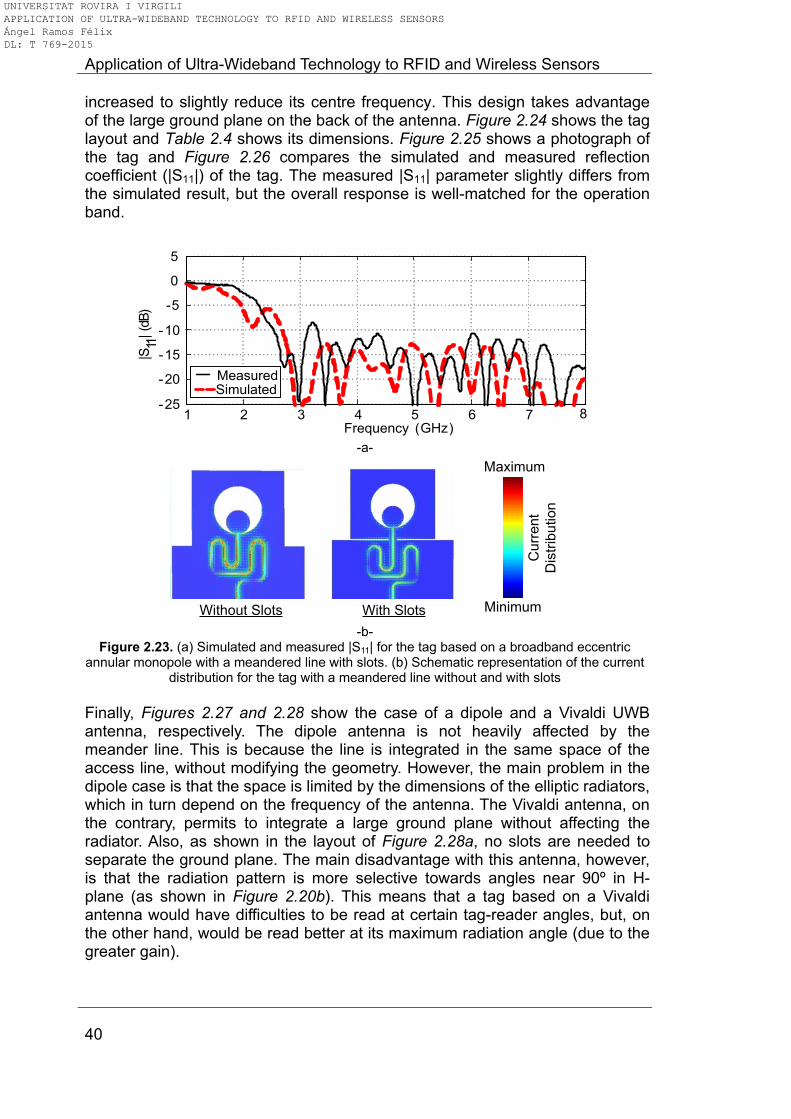
Application of Ultra-Wideband Technology to RFID and Wireless Sensors
40
increased to slightly reduce its centre frequency. This design takes advantage of the large ground plane on the back of the antenna. Figure 2.24 shows the tag layout and Table 2.4 shows its dimensions. Figure 2.25 shows a photograph of the tag and Figure 2.26 compares the simulated and measured reflection coefficient (|S11|) of the tag. The measured |S11| parameter slightly differs from the simulated result, but the overall response is well-matched for the operation band.
1 2 3 4 5 6 7 8-25
-20
-15
-10
-5
0
5
Frequency (GHz)
|S11
(dB
)
MeasuredSimulated
|
-a-
Maximum
Curr
ent
Dis
trib
ution
MinimumWithout Slots With Slots
-b- Figure 2.23. (a) Simulated and measured |S11| for the tag based on a broadband eccentric
annular monopole with a meandered line with slots. (b) Schematic representation of the current distribution for the tag with a meandered line without and with slots
Finally, Figures 2.27 and 2.28 show the case of a dipole and a Vivaldi UWB antenna, respectively. The dipole antenna is not heavily affected by the meander line. This is because the line is integrated in the same space of the access line, without modifying the geometry. However, the main problem in the dipole case is that the space is limited by the dimensions of the elliptic radiators, which in turn depend on the frequency of the antenna. The Vivaldi antenna, on the contrary, permits to integrate a large ground plane without affecting the radiator. Also, as shown in the layout of Figure 2.28a, no slots are needed to separate the ground plane. The main disadvantage with this antenna, however, is that the radiation pattern is more selective towards angles near 90º in H-plane (as shown in Figure 2.20b). This means that a tag based on a Vivaldi antenna would have difficulties to be read at certain tag-reader angles, but, on the other hand, would be read better at its maximum radiation angle (due to the greater gain).
UNIVERSITAT ROVIRA I VIRGILI APPLICATION OF ULTRA-WIDEBAND TECHNOLOGY TO RFID AND WIRELESS SENSORS Ángel Ramos Félix DL: T 769-2015
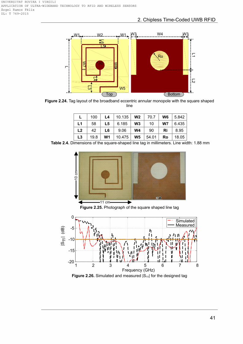
2. Chipless Time-Coded UWB RFID
41
W1 W2 W1 W3 W3W4
Ro
Ri
L1
L2
L
W5
W6
W7
L3
L4
L5
L6
Top Bottom
Figure 2.24. Tag layout of the broadband eccentric annular monopole with the square shaped line
L 100 L4 10.135 W2 70.7 W6 5.842
L1 58 L5 6.185 W3 10 W7 6.435
L2 42 L6 9.06 W4 90 Ri 8.95
L3 19.8 W1 10.475 W5 54.01 Ro 18.05
Table 2.4. Dimensions of the square-shaped line tag in millimeters. Line width: 1.88 mm
Figure 2.25. Photograph of the square shaped line tag
1 2 3 4 5 6 7 8-20
-15
-10
-5
0
Frequency (GHz)
|S11
| (
dB
)
SimulatedMeasured
Figure 2.26. Simulated and measured |S11| for the designed tag
11 cm
10 c
m
UNIVERSITAT ROVIRA I VIRGILI APPLICATION OF ULTRA-WIDEBAND TECHNOLOGY TO RFID AND WIRELESS SENSORS Ángel Ramos Félix DL: T 769-2015
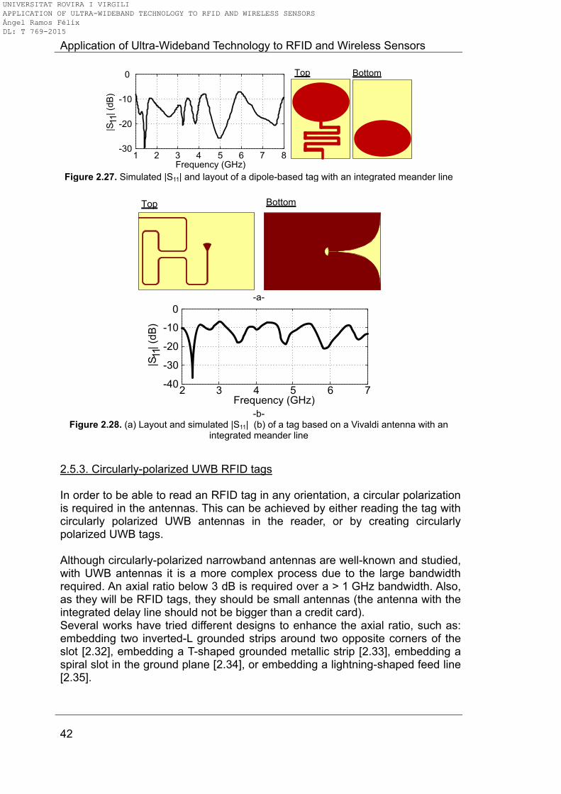
Application of Ultra-Wideband Technology to RFID and Wireless Sensors
42
Top Bottom
1 2 3 4 5 6 7 8-30
-20
-10
0
Frequency (GHz)
|S11
| (d
B)
Figure 2.27. Simulated |S11| and layout of a dipole-based tag with an integrated meander line
Top Bottom
-a-
2 3 4 5 6 7-40
-30
-20
-10
0
Frequency (GHz)
|S11
| (d
B)
-b-
Figure 2.28. (a) Layout and simulated |S11| (b) of a tag based on a Vivaldi antenna with an integrated meander line
2.5.3. Circularly-polarized UWB RFID tags In order to be able to read an RFID tag in any orientation, a circular polarization is required in the antennas. This can be achieved by either reading the tag with circularly polarized UWB antennas in the reader, or by creating circularly polarized UWB tags. Although circularly-polarized narrowband antennas are well-known and studied, with UWB antennas it is a more complex process due to the large bandwidth required. An axial ratio below 3 dB is required over a > 1 GHz bandwidth. Also, as they will be RFID tags, they should be small antennas (the antenna with the integrated delay line should not be bigger than a credit card). Several works have tried different designs to enhance the axial ratio, such as: embedding two inverted-L grounded strips around two opposite corners of the slot [2.32], embedding a T-shaped grounded metallic strip [2.33], embedding a spiral slot in the ground plane [2.34], or embedding a lightning-shaped feed line [2.35].
UNIVERSITAT ROVIRA I VIRGILI APPLICATION OF ULTRA-WIDEBAND TECHNOLOGY TO RFID AND WIRELESS SENSORS Ángel Ramos Félix DL: T 769-2015
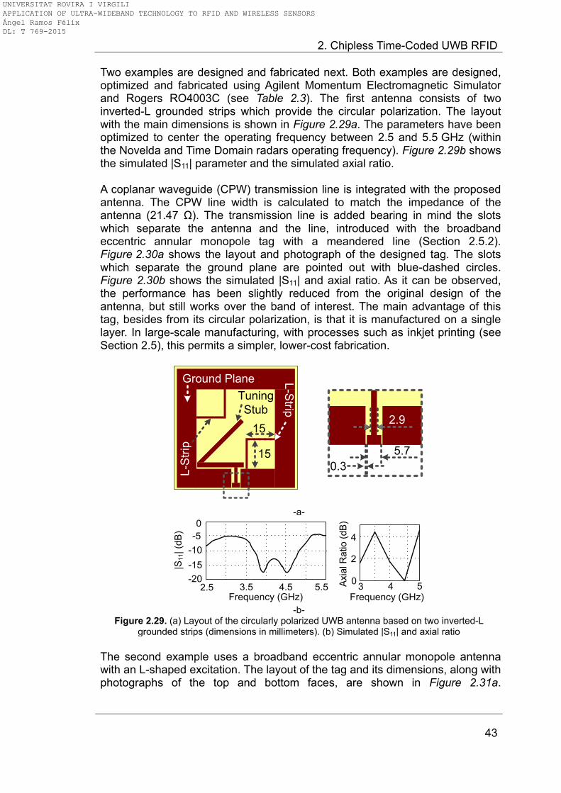
2. Chipless Time-Coded UWB RFID
43
Two examples are designed and fabricated next. Both examples are designed, optimized and fabricated using Agilent Momentum Electromagnetic Simulator and Rogers RO4003C (see Table 2.3). The first antenna consists of two inverted-L grounded strips which provide the circular polarization. The layout with the main dimensions is shown in Figure 2.29a. The parameters have been optimized to center the operating frequency between 2.5 and 5.5 GHz (within the Novelda and Time Domain radars operating frequency). Figure 2.29b shows the simulated |S11| parameter and the simulated axial ratio. A coplanar waveguide (CPW) transmission line is integrated with the proposed antenna. The CPW line width is calculated to match the impedance of the antenna (21.47 Ω). The transmission line is added bearing in mind the slots which separate the antenna and the line, introduced with the broadband eccentric annular monopole tag with a meandered line (Section 2.5.2). Figure 2.30a shows the layout and photograph of the designed tag. The slots which separate the ground plane are pointed out with blue-dashed circles. Figure 2.30b shows the simulated |S11| and axial ratio. As it can be observed, the performance has been slightly reduced from the original design of the antenna, but still works over the band of interest. The main advantage of this tag, besides from its circular polarization, is that it is manufactured on a single layer. In large-scale manufacturing, with processes such as inkjet printing (see Section 2.5), this permits a simpler, lower-cost fabrication.
0.3
2.9
15
15
5.7
Tuning
Stub
Ground Plane
L-S
trip
L-S
trip
-a-
3.5 4.52.5 5.5-20
-10
0
Frequency (GHz)
|S11| (d
B)
-5
-152
Axia
l R
atio (
dB
)
4
03 4 5
Frequency (GHz) -b-
Figure 2.29. (a) Layout of the circularly polarized UWB antenna based on two inverted-L grounded strips (dimensions in millimeters). (b) Simulated |S11| and axial ratio
The second example uses a broadband eccentric annular monopole antenna with an L-shaped excitation. The layout of the tag and its dimensions, along with photographs of the top and bottom faces, are shown in Figure 2.31a.
UNIVERSITAT ROVIRA I VIRGILI APPLICATION OF ULTRA-WIDEBAND TECHNOLOGY TO RFID AND WIRELESS SENSORS Ángel Ramos Félix DL: T 769-2015

Application of Ultra-Wideband Technology to RFID and Wireless Sensors
44
Figure 2.31b shows the simulated |S11| parameter and the simulated axial ratio. As it can be observed, there is a slightly better performance than the previous CPW-fed antenna. However, the tag size in this case (about 182x124 mm) is unpractical. This tag is, therefore, used as a reference tag with circular polarization.
-a-
2
Axia
l R
atio
(d
B)
4
03 4 5
Frequency (GHz)
6
3.5 4.52.5 5.5
-20
-10
Frequency (GHz)
|S1
1| (d
B)
-5
-15
-25
-b-
Figure 2.30. (a) Layout and photograph of the circularly polarized UWB tag based on two inverted-L grounded strips. (b) Simulated |S11| and axial ratio
2.6. Characterization of chipless time-coded UWB tags The designed chipless time-coded UWB tags in Section 2.5 are characterized in time domain. The resolution to code an ID, the influence of the material where the tag is attached to, the tag-reader angle and the polarization are studied. Finally, some tags are realized in a flexible substrate, in order to study the effects of bending. 2.6.1. Time-domain response: distance and resolution Four tags based on the broadband eccentric annular monopole with the meandered line and slots (A, B, C and D) are fabricated. They have identical size with different delay line lengths L (209, 237, 265, and 293 mm, respectively). The delay lines are terminated with an open circuit. Figure 2.32 shows the four prototypes. Figure 2.33a shows the measured tag responses using the step-frequency approach, and Figure 2.33b shows the same responses using the impulse approach (with the Geozondas radar, see Section
UNIVERSITAT ROVIRA I VIRGILI APPLICATION OF ULTRA-WIDEBAND TECHNOLOGY TO RFID AND WIRELESS SENSORS Ángel Ramos Félix DL: T 769-2015
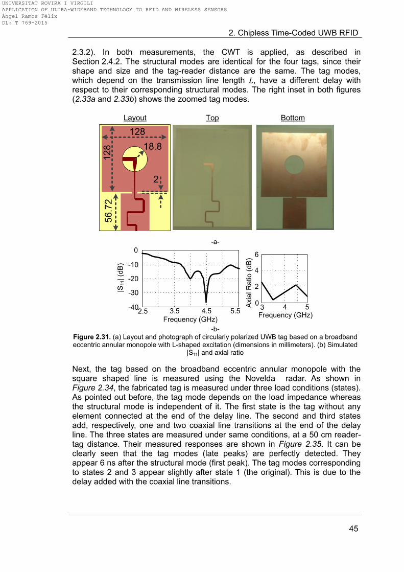
2. Chipless Time-Coded UWB RFID
45
2.3.2). In both measurements, the CWT is applied, as described in Section 2.4.2. The structural modes are identical for the four tags, since their shape and size and the tag-reader distance are the same. The tag modes, which depend on the transmission line length L, have a different delay with respect to their corresponding structural modes. The right inset in both figures (2.33a and 2.33b) shows the zoomed tag modes.
Top BottomLayout
12
8
128
56
.72
2
18.8
-a-
3.5 4.52.5 5.5
-20
-10
Frequency (GHz)
|S1
1| (d
B)
0
-30
-40
2
Axia
l R
atio (
dB
)
4
03 4 5Frequency (GHz)
6
-b-
Figure 2.31. (a) Layout and photograph of circularly polarized UWB tag based on a broadband eccentric annular monopole with L-shaped excitation (dimensions in millimeters). (b) Simulated
|S11| and axial ratio
Next, the tag based on the broadband eccentric annular monopole with the square shaped line is measured using the Novelda radar. As shown in Figure 2.34, the fabricated tag is measured under three load conditions (states). As pointed out before, the tag mode depends on the load impedance whereas the structural mode is independent of it. The first state is the tag without any element connected at the end of the delay line. The second and third states add, respectively, one and two coaxial line transitions at the end of the delay line. The three states are measured under same conditions, at a 50 cm reader-tag distance. Their measured responses are shown in Figure 2.35. It can be clearly seen that the tag modes (late peaks) are perfectly detected. They appear 6 ns after the structural mode (first peak). The tag modes corresponding to states 2 and 3 appear slightly after state 1 (the original). This is due to the delay added with the coaxial line transitions.
UNIVERSITAT ROVIRA I VIRGILI APPLICATION OF ULTRA-WIDEBAND TECHNOLOGY TO RFID AND WIRELESS SENSORS Ángel Ramos Félix DL: T 769-2015

Application of Ultra-Wideband Technology to RFID and Wireless Sensors
46
A B C D
209 mm 237 mm 265 mm 293 mm Figure 2.32. Photographs of the four prototypes (A, B, C and D) of time-coded chipless tags
based on broadband eccentric annular monopoles with a meandered line
0 2 4 6 8 10 12 140
0.2
0.4
0.6
0.8
1
Time (ns)
Norm
aliz
ed A
mplit
ude
6 6.5 7 7.5 8 8.5 90
0.04
0.08
0.12
0.16
0.2
Time (ns)
Norm
aliz
ed A
mplit
ude
ABCD
Tag Modes
Structural Modes
-a-
0 1 2 3 4 5 6 70
0.2
0.4
0.6
0.8
1
Time (ns)
No
rmaliz
ed
Am
plit
ude
4 4.5 5 5.5 60
0.04
0.08
0.12
0.16
Time (ns)
No
rmaliz
ed A
mp
litu
de
ABCD
Tag Modes
Structural
Modes
-b-
Figure 2.33. Processed time-domain measurement of the tags based on broadband eccentric annular monopoles with a meandered line, (a) using the step-frequency approach, and (b)
using the impulse-based approach
Figure 2.36 shows the measured time-domain response for distances from 50 cm to 130 cm, in steps of 10 cm. The early reflections (marked with green arrows) correspond to the structural mode, while the late ones (marked with red arrows in the top right inset) correspond to the tag modes. Due to the free-space propagation attenuation, the structural and tag modes decrease when the distance is increased. Amplitudes are normalized with respect to the 50 cm
UNIVERSITAT ROVIRA I VIRGILI APPLICATION OF ULTRA-WIDEBAND TECHNOLOGY TO RFID AND WIRELESS SENSORS Ángel Ramos Félix DL: T 769-2015
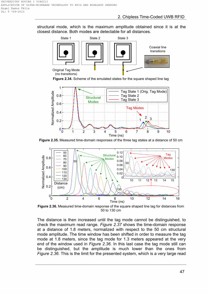
2. Chipless Time-Coded UWB RFID
47
structural mode, which is the maximum amplitude obtained since it is at the closest distance. Both modes are detectable for all distances.
State 1 State 2 State 3
Coaxial line
transitions
Original Tag Mode
(no transitions)
Figure 2.34. Scheme of the emulated states for the square shaped line tag
0 1 2 3 4 5 6 7 8 9 100
0.2
0.4
0.6
0.8
1
Time (ns)
No
rmaliz
ed A
mplit
ude
Tag State 1 (Orig. Tag Mode)
Tag State 2Tag State 3
Structural
Modes
Tag Modes
12 3
Figure 2.35. Measured time-domain responses of the three tag states at a distance of 50 cm
0 2 4 6 8 10 12 14 160
0.2
0.4
0.6
0.8
1
Time (ns)
No
rma
lize
d A
mp
litu
de
5060708090
100110120130 10 11 12 13 14 15
0
0.02
0.04
0.06
0.08
0.10
0.12
Structural
Modes
Tag
Modes
Distance
(cm)
50
130
50
130
Figure 2.36. Measured time-domain response of the square shaped line tag for distances from
50 to 130 cm
The distance is then increased until the tag mode cannot be distinguished, to check the maximum read range. Figure 2.37 shows the time-domain response at a distance of 1.8 meters, normalized with respect to the 50 cm structural mode amplitude. The time window has been shifted in order to measure the tag mode at 1.8 meters, since the tag mode for 1.3 meters appeared at the very end of the window used in Figure 2.36. In this last case the tag mode still can be distinguished, but the amplitude is much lower than the ones from Figure 2.36. This is the limit for the presented system, which is a very large read
UNIVERSITAT ROVIRA I VIRGILI APPLICATION OF ULTRA-WIDEBAND TECHNOLOGY TO RFID AND WIRELESS SENSORS Ángel Ramos Félix DL: T 769-2015

Application of Ultra-Wideband Technology to RFID and Wireless Sensors
48
range for a chipless integrated tag. Previous work [2.30] shows that an emulated tag (using a UWB antenna connected to a coaxial transmission line) can be read up to two meters. However, when measuring a real tag where the delay is integrated into the substrate the response worsens. Moreover, the integrated delay line on Rogers RO4003C has more losses than a coaxial transmission line, reducing the amplitude of the tag mode. Nevertheless, the 1.8 meters distance is much higher than the distances achieved for frequency-coded integrated chipless tags [2.36].
0 2 4 6 8 10 12 14 160
0.05
0.10
0.15
Time (ns)
No
rma
lize
d A
mp
litu
de
Structural
Mode
Tag Mode
(2nd
peak)Last distance where
the detected time
difference matches
50-130 cm cases
Figure 2.37. Measured time-domain response of the square shaped line tag at a distance of
180 cm
In order to measure the resolution experimentally, three tags based on the
broadband eccentric annular monopole with the meandered line and slots, with
a simulated delay difference of 50 ps between them are fabricated. Figure 2.38
shows their measured responses (measured with the step-frequency technique
in Figure 2.38a and with the impulse technique in Figure 2.38b). The right insets
show the zoomed tag modes. Table 2.5 depicts the measured time differences
between structural and tag modes. It can be clearly seen that a 50 ps delay
cannot be distinguished and a 100 ps delay can be distinguished with a
measurement error under 13%. Taking this result into account and since tag
sizes should be as small as possible, it is obvious that a large number of states
are not feasible. It is also important to note that the time resolution is inversely
related to the bandwidth of the system. For a 7.5 GHz bandwidth (from 3.1 to
10.6 GHz), a resolution of about 66 ps is expected. Hence, this demonstrates
that, although long delay lines have been integrated in time-coded chipless
RFID tags, this topology might be more suitable for wireless sensor applications
rather than for traditional item tagging. Frequency-coded tags, on the contrary,
have an ID space much larger [2.36-2.37].
Time Delay (ps)
Theoretical Step-Freq. Approach
Impulse-Based Approach
t1 50 77.76 38.46
t2 50 15.55 73.26
t3 100 93.31 112.7
Table 2.5. Theoretical and measured time delays for three tags with a simulated delay
UNIVERSITAT ROVIRA I VIRGILI APPLICATION OF ULTRA-WIDEBAND TECHNOLOGY TO RFID AND WIRELESS SENSORS Ángel Ramos Félix DL: T 769-2015
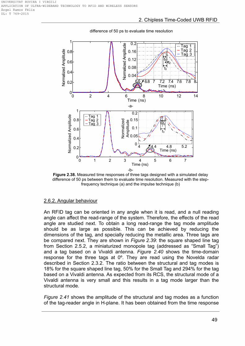
2. Chipless Time-Coded UWB RFID
49
difference of 50 ps to evaluate time resolution
0 2 4 6 8 10 12 140
0.2
0.4
0.6
0.8
1
Time (ns)
Norm
aliz
ed A
mplit
ude
6.6 6.8 7 7.2 7.4 7.6 7.8 8
0.04
0.08
0.12
0.16
0.2
Time (ns)
Norm
aliz
ed A
mplit
ude
t1t2
t3
Tag 1Tag 2Tag 3
-a-
0 1 2 3 4 5 6 70
0.2
0.4
0.6
0.8
1
Time (ns)
No
rma
lize
d A
mp
litu
de
40
0.05
0.1
0.15
0.2
Time (ns)
No
rma
lize
d
Am
plit
ud
e
4.4 4.8 5.2
t3
Tag 1Tag 2Tag 3 t1 2t
-b-
Figure 2.38. Measured time responses of three tags designed with a simulated delay difference of 50 ps between them to evaluate time resolution. Measured with the step-
frequency technique (a) and the impulse technique (b)
2.6.2. Angular behaviour An RFID tag can be oriented in any angle when it is read, and a null reading angle can affect the read-range of the system. Therefore, the effects of the read angle are studied next. To obtain a long read-range the tag mode amplitude should be as large as possible. This can be achieved by reducing the dimensions of the tag, and specially reducing the metallic area. Three tags are be compared next. They are shown in Figure 2.39: the square shaped line tag from Section 2.5.2, a miniaturized monopole tag (addressed as “Small Tag”) and a tag based on a Vivaldi antenna. Figure 2.40 shows the time-domain response for the three tags at 0º. They are read using the Novelda radar described in Section 2.3.2. The ratio between the structural and tag modes is 18% for the square shaped line tag, 50% for the Small Tag and 294% for the tag based on a Vivaldi antenna. As expected from its RCS, the structural mode of a Vivaldi antenna is very small and this results in a tag mode larger than the structural mode. Figure 2.41 shows the amplitude of the structural and tag modes as a function of the tag-reader angle in H-plane. It has been obtained from the time response
UNIVERSITAT ROVIRA I VIRGILI APPLICATION OF ULTRA-WIDEBAND TECHNOLOGY TO RFID AND WIRELESS SENSORS Ángel Ramos Félix DL: T 769-2015
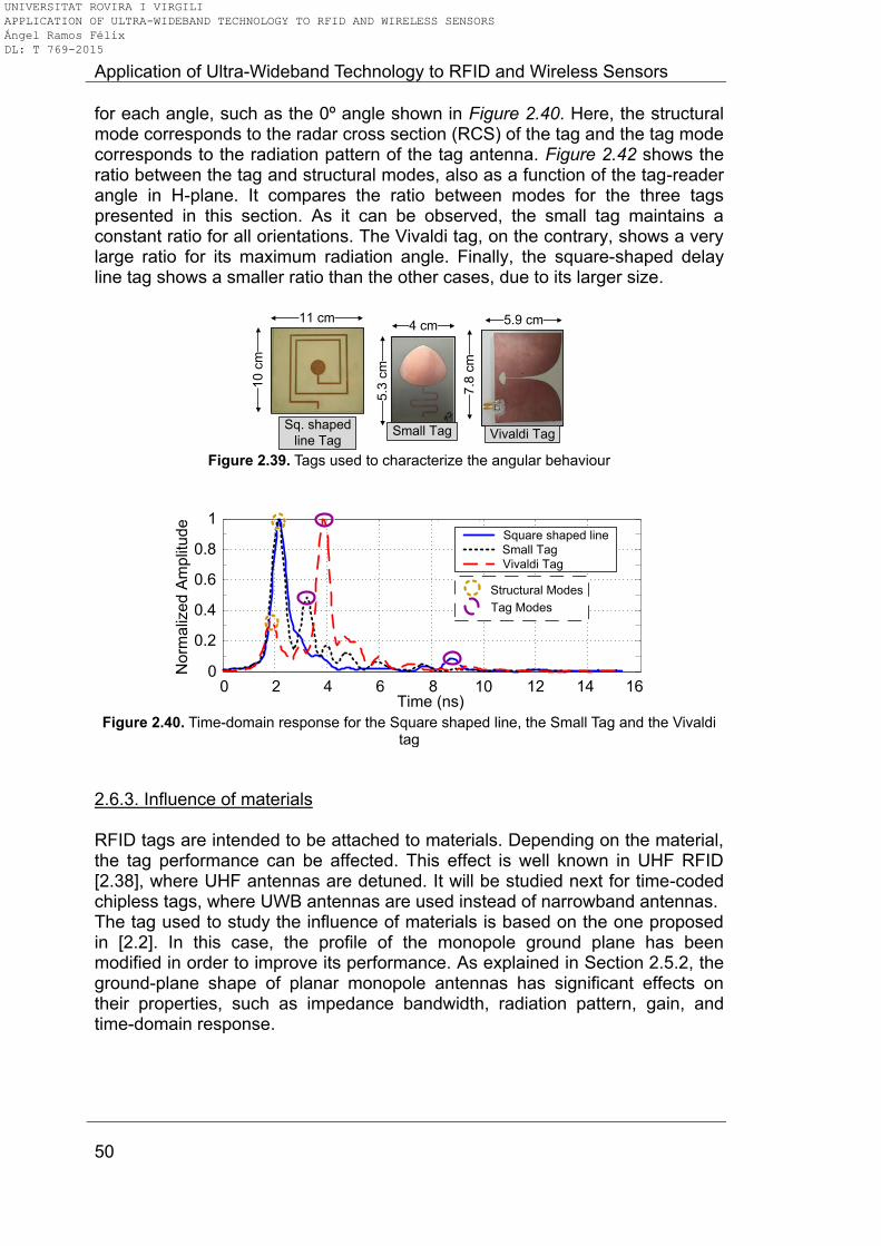
Application of Ultra-Wideband Technology to RFID and Wireless Sensors
50
for each angle, such as the 0º angle shown in Figure 2.40. Here, the structural mode corresponds to the radar cross section (RCS) of the tag and the tag mode corresponds to the radiation pattern of the tag antenna. Figure 2.42 shows the ratio between the tag and structural modes, also as a function of the tag-reader angle in H-plane. It compares the ratio between modes for the three tags presented in this section. As it can be observed, the small tag maintains a constant ratio for all orientations. The Vivaldi tag, on the contrary, shows a very large ratio for its maximum radiation angle. Finally, the square-shaped delay line tag shows a smaller ratio than the other cases, due to its larger size.
Small Tag Vivaldi TagSq. shaped
line Tag
5.3
cm
7.8
cm
5.9 cm4 cm
10 c
m
11 cm
Figure 2.39. Tags used to characterize the angular behaviour
0 2 4 6 8 10 12 14 160
0.2
0.4
0.6
0.8
1
Time (ns)
No
rmaliz
ed A
mplit
ude
Square shaped line
Small Tag
Vivaldi Tag
Structural Modes
Tag Modes
Figure 2.40. Time-domain response for the Square shaped line, the Small Tag and the Vivaldi
tag
2.6.3. Influence of materials RFID tags are intended to be attached to materials. Depending on the material, the tag performance can be affected. This effect is well known in UHF RFID [2.38], where UHF antennas are detuned. It will be studied next for time-coded chipless tags, where UWB antennas are used instead of narrowband antennas. The tag used to study the influence of materials is based on the one proposed in [2.2]. In this case, the profile of the monopole ground plane has been modified in order to improve its performance. As explained in Section 2.5.2, the ground-plane shape of planar monopole antennas has significant effects on their properties, such as impedance bandwidth, radiation pattern, gain, and time-domain response.
UNIVERSITAT ROVIRA I VIRGILI APPLICATION OF ULTRA-WIDEBAND TECHNOLOGY TO RFID AND WIRELESS SENSORS Ángel Ramos Félix DL: T 769-2015
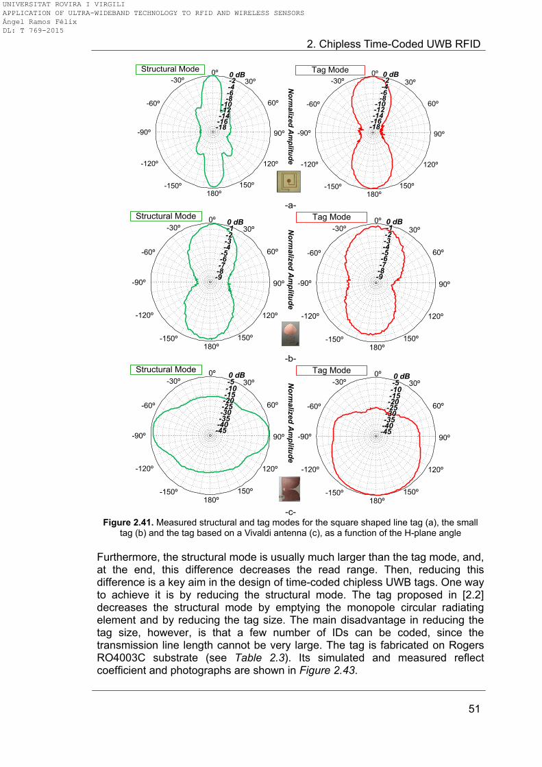
2. Chipless Time-Coded UWB RFID
51
90º
60º
30º
0º-30º
-60º
-90º
-120º
-150º180º
150º
120º
Structural Mode
No
rma
lize
d A
mp
litud
e
-18-18-16-16-14-14-12-12-10-10
-8-8-6-6-4-4-2-20 dB0 dB
90º
60º
30º
0º-30º
-60º
-90º
-120º
-150º180º
150º
120º
Tag Mode
-18-18-16-16-14-14-12-12-10-10
-8-8-6-6-4-4-2-20 dB0 dB
-a-
90º
60º
30º
0º-30º
-60º
-90º
-120º
-150º180º
150º
120º
Structural Mode
No
rma
lize
d A
mp
litud
e
-9-9-8-8-7-7-6-6-5-5-4-4-3-3
0 dB0 dB
90º
60º
30º
0º-30º
-60º
-90º
-120º
-150º180º
150º
120º
Tag Mode
-2-2-1-1
-9-9-8-8-7-7-6-6-5-5-4-4-3-3-2-2-1-10 dB0 dB
-b-
90º
60º
30º
0º-30º
-60º
-90º
-120º
-150º180º
150º
120º
Structural Mode
No
rma
lize
d A
mp
litud
e
-45-45-40-40-35-35-30-30-25-25
-15-15
0 dB0 dB
90º
60º
30º
0º-30º
-60º
-90º
-120º
-150º180º
150º
120º
Tag Mode
-10-10
-20-20
-5-5
-45-45-40-40-35-35-30-30-25-25
-15-15
0 dB0 dB
-10-10
-20-20
-5-5
-c-
Figure 2.41. Measured structural and tag modes for the square shaped line tag (a), the small tag (b) and the tag based on a Vivaldi antenna (c), as a function of the H-plane angle
Furthermore, the structural mode is usually much larger than the tag mode, and, at the end, this difference decreases the read range. Then, reducing this difference is a key aim in the design of time-coded chipless UWB tags. One way to achieve it is by reducing the structural mode. The tag proposed in [2.2] decreases the structural mode by emptying the monopole circular radiating element and by reducing the tag size. The main disadvantage in reducing the tag size, however, is that a few number of IDs can be coded, since the transmission line length cannot be very large. The tag is fabricated on Rogers RO4003C substrate (see Table 2.3). Its simulated and measured reflect coefficient and photographs are shown in Figure 2.43.
UNIVERSITAT ROVIRA I VIRGILI APPLICATION OF ULTRA-WIDEBAND TECHNOLOGY TO RFID AND WIRELESS SENSORS Ángel Ramos Félix DL: T 769-2015
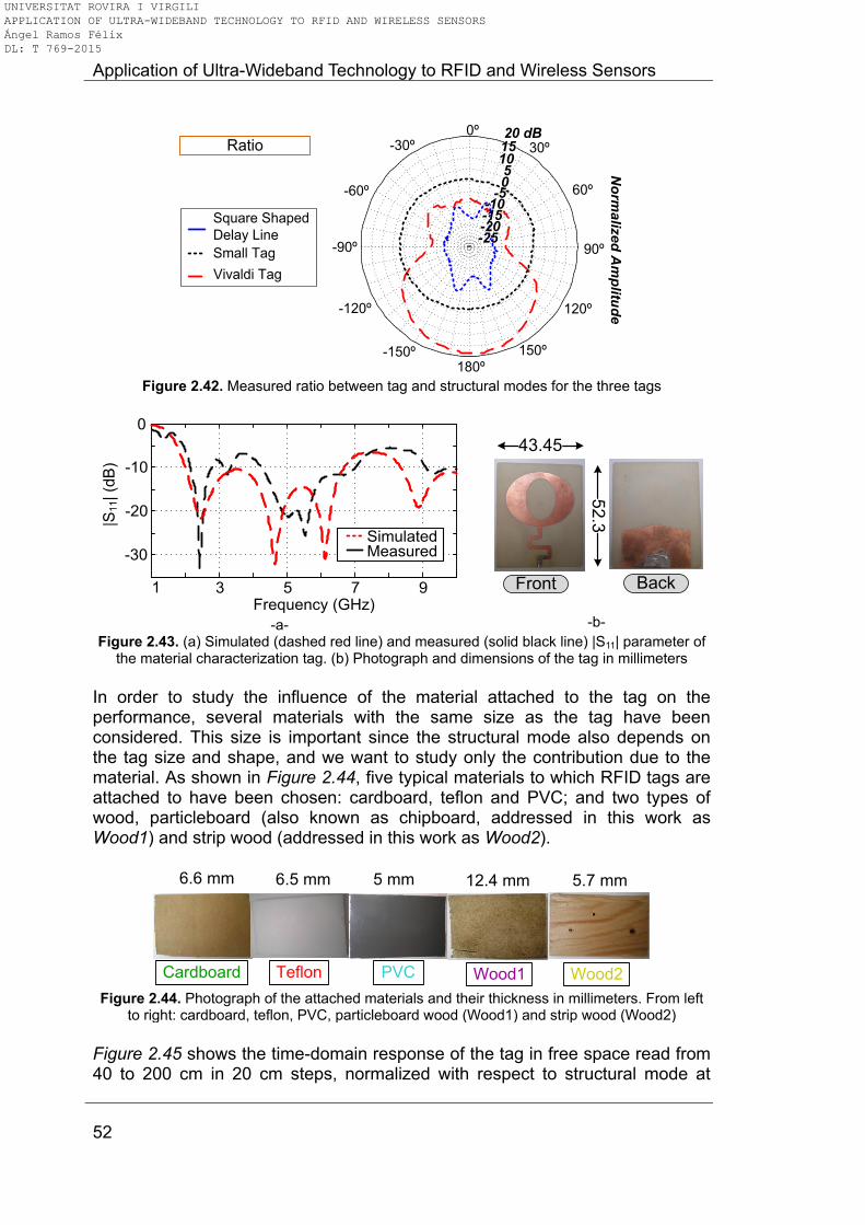
Application of Ultra-Wideband Technology to RFID and Wireless Sensors
52
90º
60º
30º
0º-30º
-60º
-90º
-120º
-150º180º
150º
120º
Ratio
No
rma
lize
d A
mp
litud
e-25-25-20-20-15-15-10-10
55
20 dB20 dB
1010
00
1515
-5-5
Vivaldi Tag
Square Shaped
Delay Line
Small Tag
Figure 2.42. Measured ratio between tag and structural modes for the three tags
1 3 5 7 9
-30
-20
-10
0
Frequency (GHz)
|S11| (d
B)
SimulatedMeasured
-a-
BackFront
52.3
43.45
-b-
Figure 2.43. (a) Simulated (dashed red line) and measured (solid black line) |S11| parameter of the material characterization tag. (b) Photograph and dimensions of the tag in millimeters
In order to study the influence of the material attached to the tag on the performance, several materials with the same size as the tag have been considered. This size is important since the structural mode also depends on the tag size and shape, and we want to study only the contribution due to the material. As shown in Figure 2.44, five typical materials to which RFID tags are attached to have been chosen: cardboard, teflon and PVC; and two types of wood, particleboard (also known as chipboard, addressed in this work as Wood1) and strip wood (addressed in this work as Wood2).
Cardboard Teflon PVC Wood1 Wood2
6.6 mm 6.5 mm 5 mm 12.4 mm 5.7 mm
Figure 2.44. Photograph of the attached materials and their thickness in millimeters. From left
to right: cardboard, teflon, PVC, particleboard wood (Wood1) and strip wood (Wood2)
Figure 2.45 shows the time-domain response of the tag in free space read from 40 to 200 cm in 20 cm steps, normalized with respect to structural mode at
UNIVERSITAT ROVIRA I VIRGILI APPLICATION OF ULTRA-WIDEBAND TECHNOLOGY TO RFID AND WIRELESS SENSORS Ángel Ramos Félix DL: T 769-2015
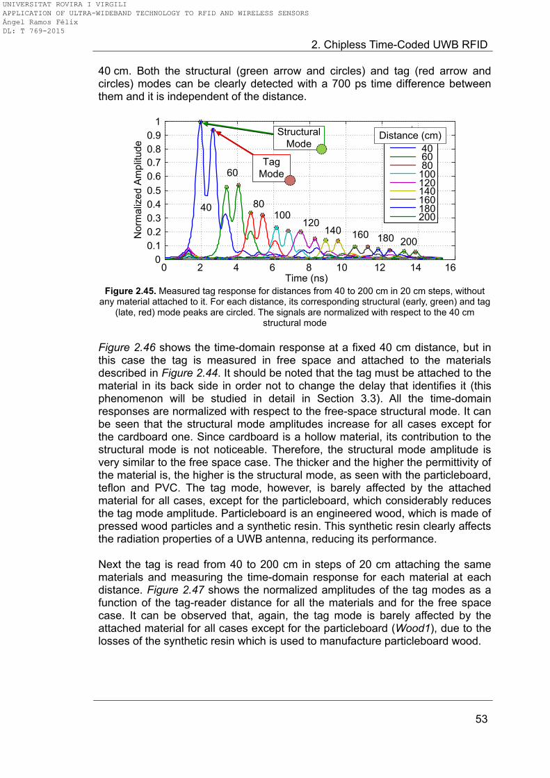
2. Chipless Time-Coded UWB RFID
53
40 cm. Both the structural (green arrow and circles) and tag (red arrow and circles) modes can be clearly detected with a 700 ps time difference between them and it is independent of the distance.
0 2 4 6 8 10 12 14 160
0.1
0.2
0.3
0.4
0.5
0.6
0.7
0.8
0.9
1
Time (ns)
No
rma
lize
d A
mp
litu
de
40 60 80100120140160180200
Distance (cm)Structural
Mode
Tag
Mode
40
60
80100
120140 160 180 200
Figure 2.45. Measured tag response for distances from 40 to 200 cm in 20 cm steps, without
any material attached to it. For each distance, its corresponding structural (early, green) and tag (late, red) mode peaks are circled. The signals are normalized with respect to the 40 cm
structural mode
Figure 2.46 shows the time-domain response at a fixed 40 cm distance, but in this case the tag is measured in free space and attached to the materials described in Figure 2.44. It should be noted that the tag must be attached to the material in its back side in order not to change the delay that identifies it (this phenomenon will be studied in detail in Section 3.3). All the time-domain responses are normalized with respect to the free-space structural mode. It can be seen that the structural mode amplitudes increase for all cases except for the cardboard one. Since cardboard is a hollow material, its contribution to the structural mode is not noticeable. Therefore, the structural mode amplitude is very similar to the free space case. The thicker and the higher the permittivity of the material is, the higher is the structural mode, as seen with the particleboard, teflon and PVC. The tag mode, however, is barely affected by the attached material for all cases, except for the particleboard, which considerably reduces the tag mode amplitude. Particleboard is an engineered wood, which is made of pressed wood particles and a synthetic resin. This synthetic resin clearly affects the radiation properties of a UWB antenna, reducing its performance. Next the tag is read from 40 to 200 cm in steps of 20 cm attaching the same materials and measuring the time-domain response for each material at each distance. Figure 2.47 shows the normalized amplitudes of the tag modes as a function of the tag-reader distance for all the materials and for the free space case. It can be observed that, again, the tag mode is barely affected by the attached material for all cases except for the particleboard (Wood1), due to the losses of the synthetic resin which is used to manufacture particleboard wood.
UNIVERSITAT ROVIRA I VIRGILI APPLICATION OF ULTRA-WIDEBAND TECHNOLOGY TO RFID AND WIRELESS SENSORS Ángel Ramos Félix DL: T 769-2015
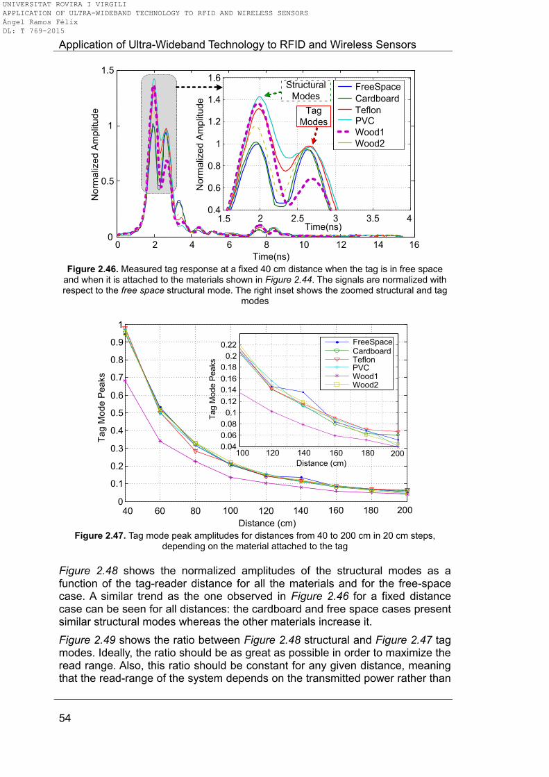
Application of Ultra-Wideband Technology to RFID and Wireless Sensors
54
0 2 4 6 8 10 12 14 160
0.5
1
1.5
Time(ns)
Norm
aliz
ed A
mplit
ude
1.5 2 2.5 3 3.5 40.4
0.6
0.8
1
1.2
1.4
1.6
Time(ns)
Norm
aliz
ed A
mplit
ude
FreeSpace
Cardboard
TeflonPVC
Wood1
Wood2
Structural
Modes
Tag
Modes
Figure 2.46. Measured tag response at a fixed 40 cm distance when the tag is in free space
and when it is attached to the materials shown in Figure 2.44. The signals are normalized with respect to the free space structural mode. The right inset shows the zoomed structural and tag
modes
0
0.1
0.2
0.3
0.4
0.5
0.6
0.7
0.8
0.9
1
Ta
g M
od
e P
ea
ks
40 60 80 100 120 140 160 180 200
Distance (cm)
0.04
0.06
0.08
0.1
0.12
0.14
0.16
0.18
0.2
0.22
Tag M
ode
Peaks
CardboardTeflonPVCWood1Wood2
FreeSpace
100 120 140 160 180 200
Distance (cm)
Figure 2.47. Tag mode peak amplitudes for distances from 40 to 200 cm in 20 cm steps,
depending on the material attached to the tag
Figure 2.48 shows the normalized amplitudes of the structural modes as a function of the tag-reader distance for all the materials and for the free-space case. A similar trend as the one observed in Figure 2.46 for a fixed distance case can be seen for all distances: the cardboard and free space cases present similar structural modes whereas the other materials increase it.
Figure 2.49 shows the ratio between Figure 2.48 structural and Figure 2.47 tag modes. Ideally, the ratio should be as great as possible in order to maximize the read range. Also, this ratio should be constant for any given distance, meaning that the read-range of the system depends on the transmitted power rather than
UNIVERSITAT ROVIRA I VIRGILI APPLICATION OF ULTRA-WIDEBAND TECHNOLOGY TO RFID AND WIRELESS SENSORS Ángel Ramos Félix DL: T 769-2015
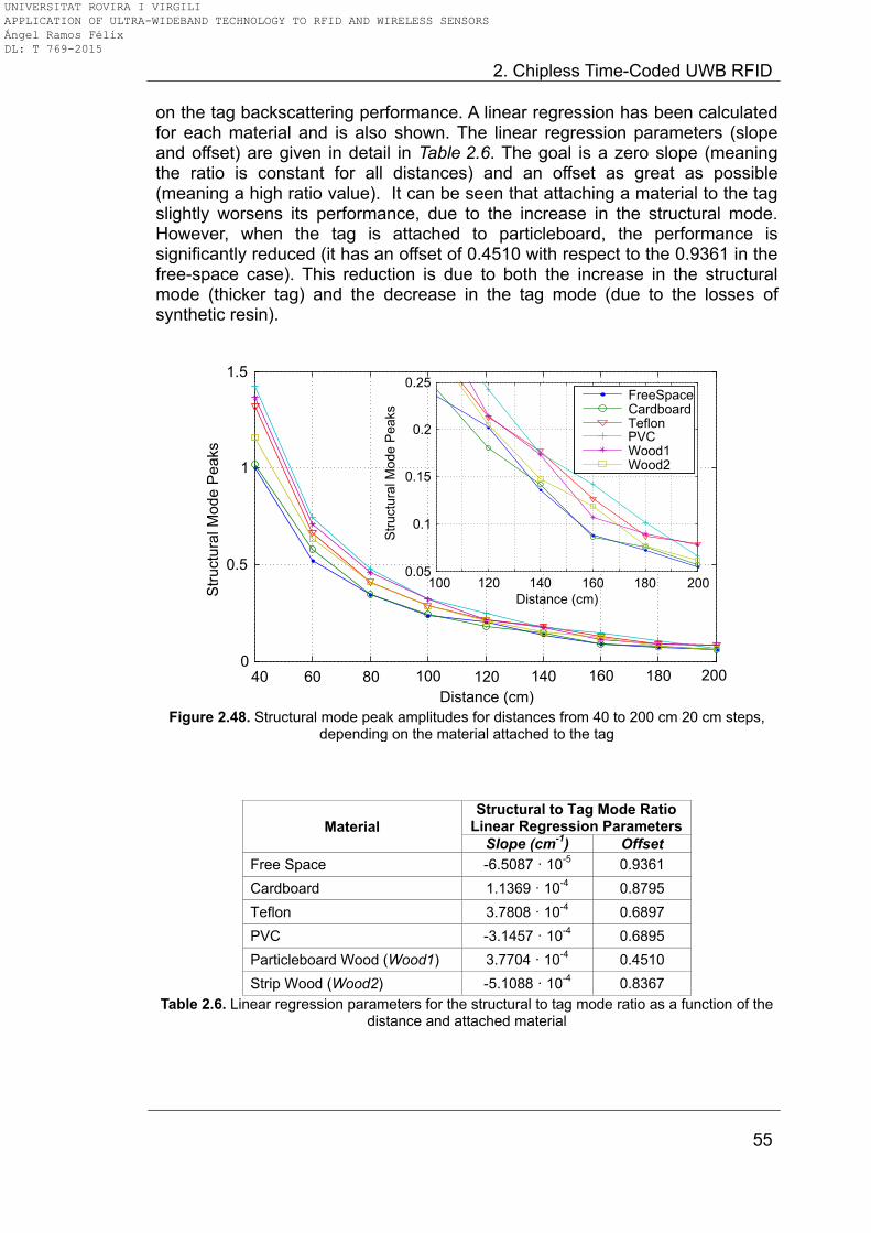
2. Chipless Time-Coded UWB RFID
55
on the tag backscattering performance. A linear regression has been calculated for each material and is also shown. The linear regression parameters (slope and offset) are given in detail in Table 2.6. The goal is a zero slope (meaning the ratio is constant for all distances) and an offset as great as possible (meaning a high ratio value). It can be seen that attaching a material to the tag slightly worsens its performance, due to the increase in the structural mode. However, when the tag is attached to particleboard, the performance is significantly reduced (it has an offset of 0.4510 with respect to the 0.9361 in the free-space case). This reduction is due to both the increase in the structural mode (thicker tag) and the decrease in the tag mode (due to the losses of synthetic resin).
40 60 80 100 120 140 160 180 2000
0.5
1
1.5
Distance (cm)
Str
uctu
ral M
od
e P
ea
ks
100 120 140 160 180 2000.05
0.1
0.15
0.2
0.25
Distance (cm)
Str
uctu
ral M
od
e P
ea
ks
FreeSpaceCardboardTeflonPVCWood1Wood2
Figure 2.48. Structural mode peak amplitudes for distances from 40 to 200 cm 20 cm steps,
depending on the material attached to the tag
Material
Structural to Tag Mode Ratio Linear Regression Parameters
Slope (cm-1
) Offset
Free Space -6.5087 · 10-5
0.9361
Cardboard 1.1369 · 10-4
0.8795
Teflon 3.7808 · 10-4
0.6897
PVC -3.1457 · 10-4
0.6895
Particleboard Wood (Wood1) 3.7704 · 10-4
0.4510
Strip Wood (Wood2) -5.1088 · 10-4
0.8367
Table 2.6. Linear regression parameters for the structural to tag mode ratio as a function of the distance and attached material
UNIVERSITAT ROVIRA I VIRGILI APPLICATION OF ULTRA-WIDEBAND TECHNOLOGY TO RFID AND WIRELESS SENSORS Ángel Ramos Félix DL: T 769-2015

Application of Ultra-Wideband Technology to RFID and Wireless Sensors
56
0.4
0.5
0.6
0.7
0.8
0.9
1
1.1
40 60 80 100 120 140 160 180 200
Distance (cm)
Str
uctu
ral to
Tag M
ode R
atio
CardboardTeflon
PVCWood1Wood2
FreeSpaceLinear
Regression
Figure 2.49. Structural to tag mode ratios for distances from 40 to 200 cm in 20 cm steps,
depending on the material attached to the tag (solid lines). Linear regression for each material (dashed lines)
Figures 2.50 and 2.51 show the structural and tag modes as a function of the tag-reader H-plane angle (φ), normalized with respect to the maximum structural and tag modes in free space, respectively. This is shown for the free space case and the particleboard (Wood1) case. The structural mode in Figure 2.50 can be seen as the radar cross section (RCS) of the tag. It is increased due to the presence of the particleboard, specially in 90º/-90º orientations, where it is very low for the free space case. As a first approximation, the structural mode is similar to a flat plate. Thus, its RCS is
given by 2 24 ( cos( )) /RCS A , where A is the area of the plate and
/ rc f is the wavelength (c is the speed of light in vacuum, f is the
operating frequency and εr is the dielectric permittivity). The wavelength λ decreases when εr increases, and therefore the RCS is larger with the attached material. In addition, the shape of structural mode diagram changes because of the constructive interference between the front and back reflections due to the thickness of the material.
The tag mode in Figure 2.51 can be seen as the radiation pattern of the antenna. In this case, the pattern changes from an omnidirectional pattern to a more directive one.
2.6.4. Polarization The polarization of several tags will be characterized next. A small monopole (Section 2.6.2), a Vivaldi tag (Section 2.5.2) and the circularly-polarized tags (Section 2.5.3) are compared. Figure 2.52a shows a scheme of the measurement: the tags are placed on a rotatory table, oriented towards the
UNIVERSITAT ROVIRA I VIRGILI APPLICATION OF ULTRA-WIDEBAND TECHNOLOGY TO RFID AND WIRELESS SENSORS Ángel Ramos Félix DL: T 769-2015

2. Chipless Time-Coded UWB RFID
57
reader’s antennas on their maximum H-plane angle. Figure 2.52b shows the tag mode as a function of the polarization angle. As it can be observed, the Vivaldi antenna is strongly polarized, and the tag mode cannot be read for cross polarization angles (-90º/90º). The small monopole also shows that for cross-polarization angles (0º/180º) there is a significant reduction in the tag mode amplitude. The tag mode amplitudes of the circularly-polarized tags show a fairly constant behaviour for all polarizations.
-14-12-10-8-6-4-2024 dB
90º
60º
30º
0º-30º
-60º
-90º
-120º
-150º180º
150º
120º
Wood1FreeSpace0 dB
Structural Mode
No
rma
lize
d A
mp
ltiud
e
(to S
truc
t. Mo
de
, Fre
eS
pa
ce
)
Figure 2.50. Structural mode as a function of the tag-reader H-plane angle, depending on the
material used. All amplitudes are normalized with respect to the maximum of the structural mode in free space
90º
60º
30º-30º
-60º
-90º
-120º
-150º
180º
150º
120º
Wood1FreeSpace0 dB
Tag Mode
No
rma
lize
d A
mp
ltiud
e
(to T
ag
Mo
de
, Fre
eS
pa
ce
)
-16-14-12-10
-8-6-4-202 dB0º
Figure 2.51. Tag mode as a function of the tag-reader H-plane angle, depending on the material used. All amplitudes are normalized with respect to the maximum of the tag mode in free space
2.6.5. Flexible substrates: bending One desirable feature with RFID tags is the ability to bend them and still obtain a reliable read. This is interesting when the tag is attached to non-flat surfaces,
UNIVERSITAT ROVIRA I VIRGILI APPLICATION OF ULTRA-WIDEBAND TECHNOLOGY TO RFID AND WIRELESS SENSORS Ángel Ramos Félix DL: T 769-2015
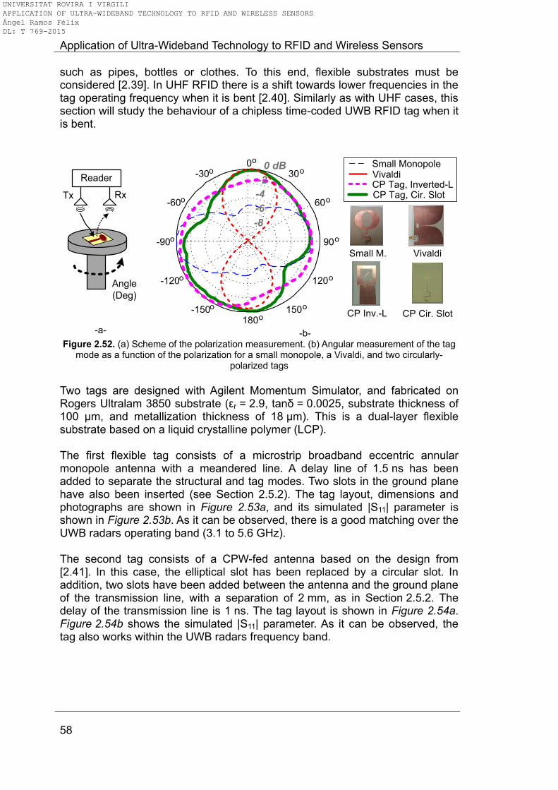
Application of Ultra-Wideband Technology to RFID and Wireless Sensors
58
such as pipes, bottles or clothes. To this end, flexible substrates must be considered [2.39]. In UHF RFID there is a shift towards lower frequencies in the tag operating frequency when it is bent [2.40]. Similarly as with UHF cases, this section will study the behaviour of a chipless time-coded UWB RFID tag when it is bent.
Reader
Tx Rx
Angle
(Deg)
-a-
-8
-4
0 dB
90o
60o
30o0o
-30o
-60o
-90o
-120o
-150o
180o150o
120o
Small MonopoleVivaldiCP Tag, Inverted-L-2
-6
Small M. Vivaldi
CP Inv.-L
CP Tag, Cir. Slot
CP Cir. Slot
-b- Figure 2.52. (a) Scheme of the polarization measurement. (b) Angular measurement of the tag
mode as a function of the polarization for a small monopole, a Vivaldi, and two circularly-polarized tags
Two tags are designed with Agilent Momentum Simulator, and fabricated on Rogers Ultralam 3850 substrate (εr = 2.9, tanδ = 0.0025, substrate thickness of 100 μm, and metallization thickness of 18 μm). This is a dual-layer flexible substrate based on a liquid crystalline polymer (LCP). The first flexible tag consists of a microstrip broadband eccentric annular monopole antenna with a meandered line. A delay line of 1.5 ns has been added to separate the structural and tag modes. Two slots in the ground plane have also been inserted (see Section 2.5.2). The tag layout, dimensions and photographs are shown in Figure 2.53a, and its simulated |S11| parameter is shown in Figure 2.53b. As it can be observed, there is a good matching over the UWB radars operating band (3.1 to 5.6 GHz). The second tag consists of a CPW-fed antenna based on the design from [2.41]. In this case, the elliptical slot has been replaced by a circular slot. In addition, two slots have been added between the antenna and the ground plane of the transmission line, with a separation of 2 mm, as in Section 2.5.2. The delay of the transmission line is 1 ns. The tag layout is shown in Figure 2.54a. Figure 2.54b shows the simulated |S11| parameter. As it can be observed, the tag also works within the UWB radars frequency band.
UNIVERSITAT ROVIRA I VIRGILI APPLICATION OF ULTRA-WIDEBAND TECHNOLOGY TO RFID AND WIRELESS SENSORS Ángel Ramos Félix DL: T 769-2015
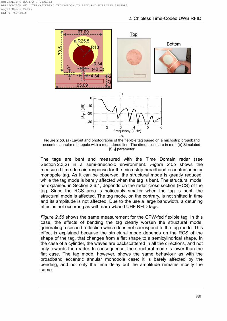
2. Chipless Time-Coded UWB RFID
59
R18
R25.5
70.5
67.09
4.34
0.34
(40 Ω)3
22.7
2
95.09
Top
Bottom
-a-
1 2 3 4 5 6
-30
-20
-10
0
Frequency (GHz)
|S11
| (d
B)
-b-
Figure 2.53. (a) Layout and photographs of the fleixble tag based on a microstrip broadband eccentric annular monopole with a meandered line. The dimensions are in mm. (b) Simulated
|S11| parameter
The tags are bent and measured with the Time Domain radar (see Section 2.3.2) in a semi-anechoic environment. Figure 2.55 shows the measured time-domain response for the microstrip broadband eccentric annular monopole tag. As it can be observed, the structural mode is greatly reduced, while the tag mode is barely affected when the tag is bent. The structural mode, as explained in Section 2.6.1, depends on the radar cross section (RCS) of the tag. Since the RCS area is noticeably smaller when the tag is bent, the structural mode is affected. The tag mode, on the contrary, is not shifted in time and its amplitude is not affected. Due to the use a large bandwidth, a detuning effect is not occurring as with narrowband UHF RFID tags. Figure 2.56 shows the same measurement for the CPW-fed flexible tag. In this case, the effects of bending the tag clearly worsen the structural mode, generating a second reflection which does not correspond to the tag mode. This effect is explained because the structural mode depends on the RCS of the shape of the tag, that changes from a flat shape to a semicylindrical shape. In the case of a cylinder, the waves are backscattered in all the directions, and not only towards the reader. In consequence, the structural mode is lower than the flat case. The tag mode, however, shows the same behaviour as with the broadband eccentric annular monopole case: it is barely affected by the bending, and not only the time delay but the amplitude remains mostly the same.
UNIVERSITAT ROVIRA I VIRGILI APPLICATION OF ULTRA-WIDEBAND TECHNOLOGY TO RFID AND WIRELESS SENSORS Ángel Ramos Félix DL: T 769-2015

Application of Ultra-Wideband Technology to RFID and Wireless Sensors
60
70.7
2
58 27
2.8
5
5
10
58
49.8
9
-a-
1 2 3 4 5 6
-30
-20
-10
0
Frequency (GHz)
|S11
| (d
B)
-b-
Figure 2.54. (a) Layout and photograph of the fleixble tag based on a CPW-fed UWB antenna (dimensions in millimeters). (b) Simulated |S11| parameter
25 26 27 28 29 30 31 32 330
0.2
0.4
0.6
0.8
1
Time (ns)
No
rma
lize
d A
mp
litu
de
Structural
Modes
No bendBend 1Bend 2Bend 3Bend 4
Tag
Modes
1 2 3 4
Figure 2.55. Measured time-domain response of the flexible tag based on a broadband
eccentric annular monopole as a function of the bending on the tag
Finally, a practical example will be studied with the broadband eccentric annular monopole flexible tag, since it has shown a better robustness in terms of structural mode, and a larger structural to tag mode ratio. Figure 2.57 shows the measured time-domain response of the tag placed on top of a plastic (PET) bottle, when the bottle is empty and when it has been filled of water. As expected, the tag mode is greatly affected because of the water (as with many
UNIVERSITAT ROVIRA I VIRGILI APPLICATION OF ULTRA-WIDEBAND TECHNOLOGY TO RFID AND WIRELESS SENSORS Ángel Ramos Félix DL: T 769-2015
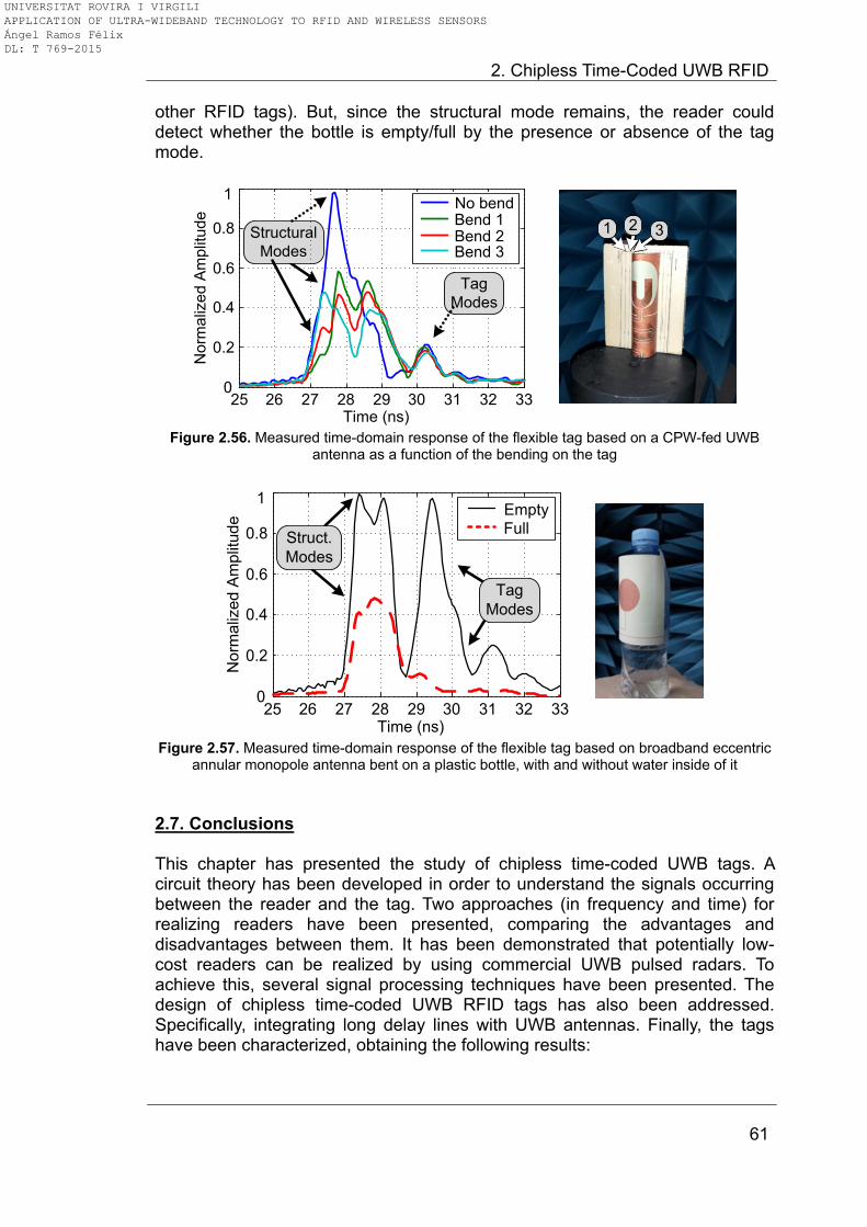
2. Chipless Time-Coded UWB RFID
61
other RFID tags). But, since the structural mode remains, the reader could detect whether the bottle is empty/full by the presence or absence of the tag mode.
25 26 27 28 29 30 31 32 330
0.2
0.4
0.6
0.8
1
Time (ns)
No
rma
lized
Am
plit
ud
e
Structural
Modes
No bendBend 1Bend 2Bend 3
Tag
Modes
1 2 3
Figure 2.56. Measured time-domain response of the flexible tag based on a CPW-fed UWB
antenna as a function of the bending on the tag
25 26 27 28 29 30 31 32 330
0.2
0.4
0.6
0.8
1
Time (ns)
No
rma
lize
d A
mp
litu
de
Struct.
Modes
Tag
Modes
EmptyFull
Figure 2.57. Measured time-domain response of the flexible tag based on broadband eccentric
annular monopole antenna bent on a plastic bottle, with and without water inside of it
2.7. Conclusions This chapter has presented the study of chipless time-coded UWB tags. A circuit theory has been developed in order to understand the signals occurring between the reader and the tag. Two approaches (in frequency and time) for realizing readers have been presented, comparing the advantages and disadvantages between them. It has been demonstrated that potentially low-cost readers can be realized by using commercial UWB pulsed radars. To achieve this, several signal processing techniques have been presented. The design of chipless time-coded UWB RFID tags has also been addressed. Specifically, integrating long delay lines with UWB antennas. Finally, the tags have been characterized, obtaining the following results:
UNIVERSITAT ROVIRA I VIRGILI APPLICATION OF ULTRA-WIDEBAND TECHNOLOGY TO RFID AND WIRELESS SENSORS Ángel Ramos Félix DL: T 769-2015
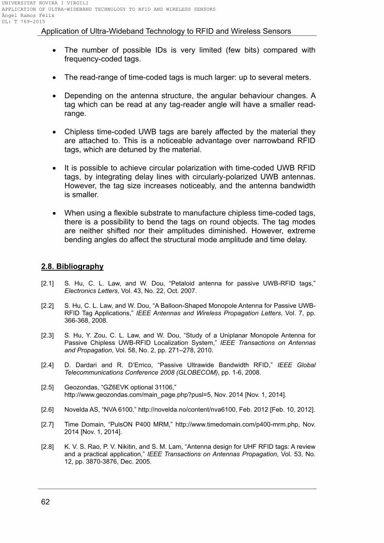
Application of Ultra-Wideband Technology to RFID and Wireless Sensors
62
The number of possible IDs is very limited (few bits) compared with frequency-coded tags.
The read-range of time-coded tags is much larger: up to several meters.
Depending on the antenna structure, the angular behaviour changes. A tag which can be read at any tag-reader angle will have a smaller read-range.
Chipless time-coded UWB tags are barely affected by the material they are attached to. This is a noticeable advantage over narrowband RFID tags, which are detuned by the material.
It is possible to achieve circular polarization with time-coded UWB RFID tags, by integrating delay lines with circularly-polarized UWB antennas. However, the tag size increases noticeably, and the antenna bandwidth is smaller.
When using a flexible substrate to manufacture chipless time-coded tags, there is a possibility to bend the tags on round objects. The tag modes are neither shifted nor their amplitudes diminished. However, extreme bending angles do affect the structural mode amplitude and time delay.
2.8. Bibliography [2.1] S. Hu, C. L. Law, and W. Dou, “Petaloid antenna for passive UWB-RFID tags,”
Electronics Letters, Vol. 43, No. 22, Oct. 2007.
[2.2] S. Hu, C. L. Law, and W. Dou, “A Balloon-Shaped Monopole Antenna for Passive UWB-RFID Tag Applications,” IEEE Antennas and Wireless Propagation Letters, Vol. 7, pp. 366-368, 2008.
[2.3] S. Hu, Y. Zou, C. L. Law, and W. Dou, “Study of a Uniplanar Monopole Antenna for Passive Chipless UWB-RFID Localization System,” IEEE Transactions on Antennas and Propagation, Vol. 58, No. 2, pp. 271–278, 2010.
[2.4] D. Dardari and R. D’Errico, “Passive Ultrawide Bandwidth RFID,” IEEE Global Telecommunications Conference 2008 (GLOBECOM), pp. 1-6, 2008.
[2.5] Geozondas, “GZ6EVK optional 31106,” http://www.geozondas.com/main_page.php?pusl=5, Nov. 2014 [Nov. 1, 2014].
[2.6] Novelda AS, “NVA 6100,” http://novelda.no/content/nva6100, Feb. 2012 [Feb. 10, 2012].
[2.7] Time Domain, “PulsON P400 MRM,” http://www.timedomain.com/p400-mrm.php, Nov. 2014 [Nov. 1, 2014].
[2.8] K. V. S. Rao, P. V. Nikitin, and S. M. Lam, “Antenna design for UHF RFID tags: A review and a practical application,” IEEE Transactions on Antennas Propagation, Vol. 53, No. 12, pp. 3870-3876, Dec. 2005.
UNIVERSITAT ROVIRA I VIRGILI APPLICATION OF ULTRA-WIDEBAND TECHNOLOGY TO RFID AND WIRELESS SENSORS Ángel Ramos Félix DL: T 769-2015
2. Chipless Time-Coded UWB RFID
63
[2.9] R. B. Green, “Relationships between antennas as scatterers and radiators,” IEEE Transactions on Antennas and Propagation, Vol. 14, No. 1, pp. 17-21, Jan. 1966.
[2.10] R.E. Collin and F. J. Zucker, “The receiving antenna,” Antenna Theory: Part 1, McGraw-Hill, New-York, 1969.
[2.11] R. C. Hansen, "Scattering from conjugate-matched antennas," Proceedings of the IEEE, Vol. 77, No. 5, pp. 659–662, May 1989.
[2.12] Y. Liu, D. M. Fu, and S. X. Gong, “A novel model for analyzing the radar cross section of microstrip antenna,” J Electromagn Waves Applic., Vol. 17, pp. 1301-1310, 2003.
[2.13] J. H. Johnson, W. Choi, and R. L. Moore, “Precision experimental characterization of the scattering and radiation properties of antennas,” IEEE Transactions on Antennas and Propagation, Vol. 30, pp. 108–112, 1982.
[2.14] Keysight Technologies, “E8364C PNA Microwave Network Analyzer,” http://www.keysight.com/en/pd-1350015-pn-E8364C/pna-microwave-network-analyzer?&cc=ES&lc=eng, Nov. 2014 [Nov. 1, 2014].
[2.15] A. Lazaro, R. Villarino, and D. Girbau, “Design of tapered slot Vivaldi antenna for UWB breast cancer detection,” Microwave and Optical Technology Letters, Vol. 53, No. 3, pp. 639-643, 2011.
[2.16] Agilent Technologies, "Agilent Time Domain Analysis Using a Network Analyzer", Application Note 1287-12, 2012.
[2.17] U. Meyer-Base, H. Natarajan, E. Castillo, and A. Garcia, "Faster than the FFT: The chirp-z RAG-n Discrete Fast Fourier Transform," Frequenz, Vol. 60, No. 7-8, pp. 147-151, 2006.
[2.18] J. D. Taylor, "Ultrawideband Radar: Applications and Design," CRC Press, 2012.
[2.19] A. Petroff, "A Pratical, High Performance Ultra-Wideband Radar Platform," IEEE Radar Conference 2012, pp. 880-884, 2012.
[2.20] R. J. Fontana, "Recent System Applications of Short-Pulse Ultra-Wideband (UWB) Technology," IEEE Transactions on Microwave Theory and Techniques, Vol. 52, No. 9, pp. 2087-2104, 2004.
[2.21] XeThru by Novelda, “XeThru X2” and “XeThru X1,” https://www.xethru.com/content/technology-0, Jan. 2015. [Jan 4, 2015].
[2.22] K. Pourvoyeur, A. Stelzer, G. Ossberger, T. Buchegger, and M. Pichler, "Wavelet-based impulse reconstruction in UWB-radar," IEEE MTT-S International Microwave Symposium 2003, pp. 603-606, 2003.
[2.23] G. Kaiser, “A friendly guide to wavelets”, Boston: Birkhauser, 1994.
[2.24] A. Lazaro, D. Girbau, and R. Villarino, “Wavelet-based breast tumor localization technique of microwave imaging using UWB,” Progress in Electromagnetic Research - PIER, Vol. 94, pp. 264-280, 2009.
[2.25] G. Shaker, S. Safavi-Naeini, N. Sangary, and M. M. Tentzeris, "Inkjet Printing of Ultrawideband (UWB) Antennas on Paper-Based Substrates," IEEE Antennas and Wireless Propagation Letters, Vol. 10, pp. 111-114, 2011.
UNIVERSITAT ROVIRA I VIRGILI APPLICATION OF ULTRA-WIDEBAND TECHNOLOGY TO RFID AND WIRELESS SENSORS Ángel Ramos Félix DL: T 769-2015
Application of Ultra-Wideband Technology to RFID and Wireless Sensors
64
[2.26] S. Angelopoulos, A. Z. Anastopoulos, D. I. Kaklamani, A. A. Alexandridis, F. Lazarakis, and K. Dangakis, “Circular and elliptical CPW-fed slot and microstrip-fed antennas for ultra wideband applications,” IEEE Antennas and Wireless Propagation Letters, Vol. 5, pp. 294–297, 2006.
[2.27] Y. H. Suh and I. Park, “A broadband eccentric annular slot antenna,” IEEE Antennas and Propagation Society Intl. Symposium, vol. 1, pp. 94-97. 2001.
[2.28] Y. Lu, Y. Huang, H. T. Chatta, and P. Cao, “Reducing Ground-Plane Effects on UWB Monopole Antennas,” IEEE Antennas and Wireless Propagation Letters, vol. 10, pp. 147-150, 2011.
[2.29] Y. Lu, Y. Huang, H. T. Chatta, Y. C. Shen, and S. J. Boyes, “An elliptical UWB monopole antenna with reduced ground plane effects,” International Workshop on Antenna Technology (iWAT), pp. 1-4. 2010.
[2.30] A. Lazaro, A. Ramos, D. Girbau, and R. Villarino, “Chipless UWB RFID Tag Detection Using Continuous Wavelet Transform,” IEEE Antennas and Wireless Propagation Letters, Vol. 10, pp. 520-523, 2011.
[2.31] A. Ramos, A. Lazaro, D. Girbau, and R. Villarino, “Time-domain measurement of time-coded UWB chipless RFID tags,” Progress in Electromagnetics Research, Vol. 116, pp. 313-331, 2011.
[2.32] J. Pourahmadazar, C. Ghobadi, J. Nourinia, N. Felegari, and H. Shirzad, “Broadband CPW-Fed Circularly Polarized Square Slot Antenna With Inverted-L Strips for UWB Applications,” IEEE Antennas and Wireless Propagation Letters, Vol. 10, pp. 369-372, 2011.
[2.33] R. P. Xu, X. D. Huang, and C.H. Cheng, “Broadband Circularly Polarized Wide-Slot Antenna,” Microwave and Optical Technology Letters, Vol. 49, No. 5, pp. 1005-1007, 2007.
[2.34] O. A. Mashaal, S. K. A. Rahim, A. Y. Abdulrahman, M. I. Sabran, M. S. A. Rani, and P. S. Hall, “A Coplanar Waveguide Fed Two Arm Archimedean Spiral Slot Antenna With Improved Bandwidth,” IEEE Transactions on Antennas and Propagation, Vol. 61, No. 2, pp. 939-943, 2013.
[2.35] J-Y. Sze, C-I. G. Hsu, Z-W. Chen, and C-C. Chang, “Broadband CPW-Fed Circularly Polarized Square Slot Antenna With Lightening-Shaped Feedline and Inverted-L Grounded Strips,” IEEE Transactions on Antennas and Propagation, Vol. 58, No. 3, pp. 973-977, 2010.
[2.36] S. Preradovic, I. Balbin, N. C. Karmakar, and G. F. Swiegers, “Multiresonator-Based Chipless RFID System for Low-Cost Item Tracking,” IEEE Transactions on Microwave Theory and Techniques, Vol. 57, No. 5, pp. 1411-1419, 2009.
[2.37] A. Vena, E. Perret, and S. Tedjini, “Chipless RFID Tag Using Hybrid Coding Technique,” IEEE Transactions on Microwave Theory and Techniques, Vol. 59, No. 12, pp. 3356-3364, Dec. 2011.
[2.38] J. Lorenzo, D. Girbau, A. Lazaro, and R. Villarino, “Read range reduction in UHF RFID due to antenna detuning and gain penalty,” Microwave and Optical Technology Letters, Vol. 53, No. 1, pp. 144-148, 2011.
[2.39] A. Rida, L. Yang, R. Vyas, and M. M. Tentzeris, "Conductive Inkjet-Printed Antennas on Flexible Low-Cost Paper-Based Substrates for RFID and WSN Applications," IEEE Antennas and Propagation Magazine, Vol. 51, No. 3, pp. 13-29, 2009.
UNIVERSITAT ROVIRA I VIRGILI APPLICATION OF ULTRA-WIDEBAND TECHNOLOGY TO RFID AND WIRELESS SENSORS Ángel Ramos Félix DL: T 769-2015

2. Chipless Time-Coded UWB RFID
65
[2.40] L. Yang, L. J. Martin, D. Staiculescu, C. P. Wong, and M. M. Tentzeris, "Conformal Magnetic Composite RFID for Wearable RF and Bio-Monitoring Applications," IEEE Transactions on Microwave Theory and Techniques, Vol. 56, No. 12, pp. 3223-3230, 2008.
[2.41] N. Tavassolian, S. Nikolaou, and M. M. Tentzeris, "A Flexible UWB Elliptical Slot Antenna with a Tuning Uneven U-shape Stub on LCP for Microwave Tumor Detection," Asia-Pacific Microwave Conference 2007, pp. 1-4, Dec. 2007.
UNIVERSITAT ROVIRA I VIRGILI APPLICATION OF ULTRA-WIDEBAND TECHNOLOGY TO RFID AND WIRELESS SENSORS Ángel Ramos Félix DL: T 769-2015
Application of Ultra-Wideband Technology to RFID and Wireless Sensors
66
UNIVERSITAT ROVIRA I VIRGILI APPLICATION OF ULTRA-WIDEBAND TECHNOLOGY TO RFID AND WIRELESS SENSORS Ángel Ramos Félix DL: T 769-2015
3. Chipless Time-Coded UWB Wireless Sensors
67
3. Chipless Time-Coded UWB Wireless Sensors 3.1. Introduction: Cost, reliability and hazardous environments Completely-passive battery-free wireless sensors are desirable in remote
sensing applications where long-term environment controlling and monitoring
take place. In addition, since they do not require either wiring or batteries, they
can be used in hazardous environments, such as contaminated areas, under
concrete, in chemical or vacuum process chambers and also in applications
with moving or rotating parts.
Chipless RFID sensor tags could be an interesting alternative for passive
wireless sensing. They consist of integrating a passive sensor into a chipless
tag. The integration of sensors in chipless tags as well as the development of
their reading systems might result into a challenging and unique opportunity in
several applications such as the ones addressed above. For instance, an
identification sensor system platform at 915 MHz for passive chipless RFID
sensor tags is proposed in [3.1] to sense ethylene gas concentration. A wireless
temperature transducer based on micro bimorph cantilevers and split ring
resonators at 30 GHz is presented in [3.2]. Passive wireless pressure
micromachined sensors are proposed in [3.3] and [3.4]. A 13-bit frequency-
coded chipless sensor based on silicone nanowires to detect both temperature
and humidity is presented in [3.5]. Chipless RFID sensor tags where the
identification code generation is realized using SAW devices have also been
addressed in a number of works; three examples of temperature sensors based
on SAW technology are proposed in [3.6-3.8].
This chapter considers chipless time-coded UWB RFID tags for wireless sensing. Two main strategies are studied: amplitude-based and delay-based. These strategies rely, respectively, on changing the tag mode amplitude or time delay depending on a physical parameter. Two sensor examples of each strategy are presented: temperature sensors and permittivity (for concrete composition detection) sensors. The chapter is organized as follows:
Section 3.2 presents amplitude-based chipless time-coded UWB sensors, specifically:
o A temperature sensor using off-the-shelf positive temperature resistors
o Temperature threshold detectors using shape memory alloys and using a thermal switch
o Detection techniques for threshold detectors o Self-calibration techniques for chipless amplitude-based sensors
Section 3.3 presents delay-based chipless time-coded UWB sensors, specifically, a permittivity sensor that enables concrete composition detection
Finally, Section 3.4 draws the conclusions of the chapter
UNIVERSITAT ROVIRA I VIRGILI APPLICATION OF ULTRA-WIDEBAND TECHNOLOGY TO RFID AND WIRELESS SENSORS Ángel Ramos Félix DL: T 769-2015

Application of Ultra-Wideband Technology to RFID and Wireless Sensors
68
3.2. Amplitude-based chipless time-coded sensors 3.2.1. Principle of operation It has been introduced in Section 2.2 that the tag mode amplitude depends on the reflection coefficient connected at the end of the transmission line. Figure 3.1a shows the circuit scheme where the tag mode amplitude is changed as a function of this reflection coefficient. The amplitude variations and the possibility of modulating them by means of a resistive sensor are shown in Figure 3.1b. In this last figure, several surface-mount (SMD, 0603) resistors are soldered at the end of the transmission line (ZLOAD), and the corresponding time-domain signal is obtained. These measurements are done at a sensor-reader distance of 50 cm, with the frequency-step approach (VNA, Section 2.3.1) and the broadband eccentric annular monopole antenna with a meandered-line slot (see Section 2.5.2). One sensor can be identified from the other by using the delay between the structural and tag modes. The structural modes remain identical for all resistors. All the tag modes appear at the same time (the transmission line length L is constant) and their amplitudes depend on the value of the resistor. It can also be observed that the higher the resistance is with respect to the transmission line characteristic impedance (Zc = 50 Ω), the lower is the reflection coefficient variation for a given temperature change. This saturation effect is expected since the tag mode amplitude depends directly on the reflection coefficient ΓLOAD. The resistance value can be obtained from the measured ratio between the structural and tag modes, STRATIO. This ratio is obtained from the peak of the tag mode amplitude normalized with respect to the peak of the structural mode amplitude. Then, a calibration technique similar to time-domain reflectometry (TDR) calibration is performed. The STRATIO for a given load resistance R can be expressed as:
( ) ( )
( ) ( )
RATIO LOAD
RATIO MAX DC MAX
ST R R
ST R R
, (3.1)
where RMAX is an arbitrary known resistance and ΓDC(RMAX) is the ideal (DC) reflection coefficient at RMAX. In order to minimize measurement errors, a value of RMAX that leads to a value of ΓDC close to unity (open circuit case) is chosen. In practice, a known high-value resistor can be used (here RMAX = 680 Ω, as shown in Figure 3.1b). ΓLOAD are the measured reflection coefficients associated to each load resistance (R), ( ) / ( )LOAD c cR Z R Z and are obtained from
(3.1). Using the tag to structural mode ratios, the measurement of the reflection coefficient (and thus the calibration) is theoretically independent from the tag-to-reader distance, as it will be addressed in Section 3.2.2. Expression (3.1) predicts a linear model between STRATIO for a given resistance and its load reflection coefficient. Finally, the estimated resistance is calculated as:
UNIVERSITAT ROVIRA I VIRGILI APPLICATION OF ULTRA-WIDEBAND TECHNOLOGY TO RFID AND WIRELESS SENSORS Ángel Ramos Félix DL: T 769-2015
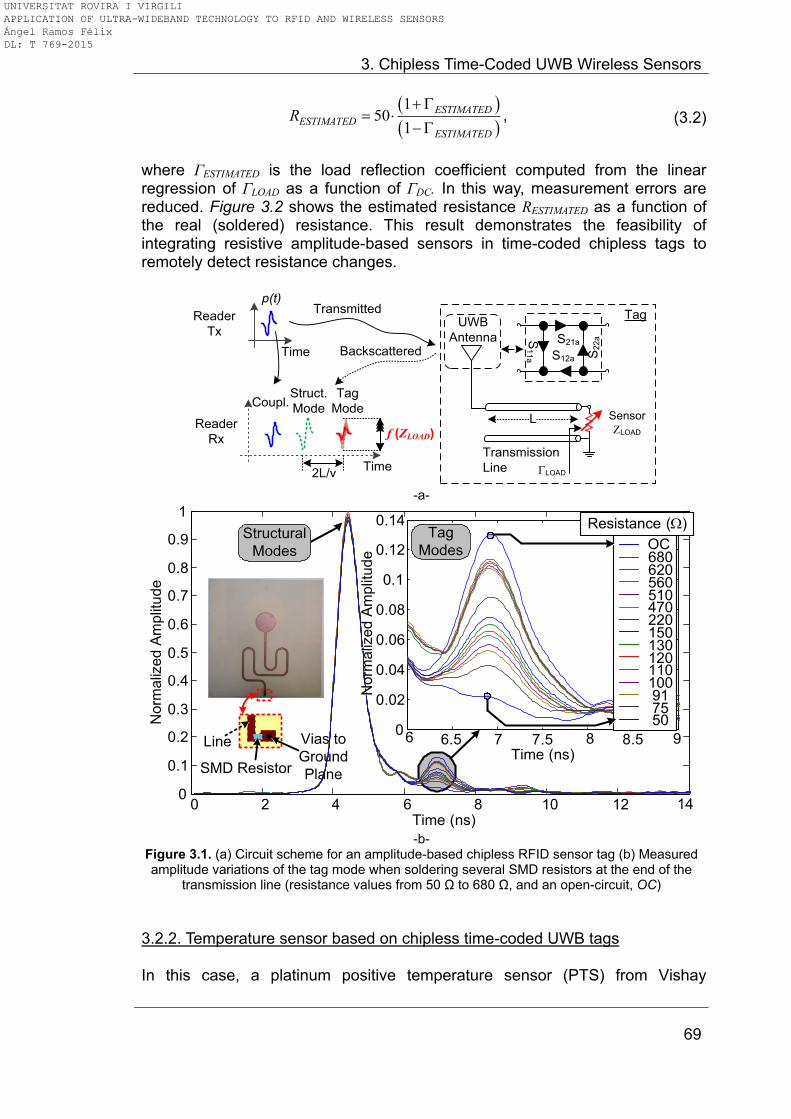
3. Chipless Time-Coded UWB Wireless Sensors
69
150
1
ESTIMATEDESTIMATED
ESTIMATED
R
, (3.2)
where ΓESTIMATED is the load reflection coefficient computed from the linear regression of ΓLOAD as a function of ΓDC. In this way, measurement errors are reduced. Figure 3.2 shows the estimated resistance RESTIMATED as a function of the real (soldered) resistance. This result demonstrates the feasibility of integrating resistive amplitude-based sensors in time-coded chipless tags to remotely detect resistance changes.
Transmission
Line
L
UWB
Antenna
Time
Struct.
Mode
Time
p(t)Transmitted
BackscatteredS21a
S12a S2
2aS
11
a
Tag
ModeCoupl.
Tag
2L/v
f (ZLOAD)
LOAD
Reader
Tx
Reader
Rx
Sensor
ZLOAD
-a-
0 2 4 6 8 10 12 140
0.1
0.2
0.3
0.4
0.5
0.6
0.7
0.8
0.9
1
Time (ns)
Norm
aliz
ed A
mplit
ud
e
6 6.5 7 7.5 8 8.5 90
0.02
0.04
0.06
0.08
0.1
0.12
0.14
Time (ns)
No
rma
lize
d A
mp
litud
eN
orm
aliz
ed
Am
plit
ude
Structural
Modes
Tag
Modes OC680620560510470220150130120110100 91 75 50
Resistance ()
Line
SMD Resistor
Vias to
Ground
Plane
-b-
Figure 3.1. (a) Circuit scheme for an amplitude-based chipless RFID sensor tag (b) Measured amplitude variations of the tag mode when soldering several SMD resistors at the end of the
transmission line (resistance values from 50 Ω to 680 Ω, and an open-circuit, OC)
3.2.2. Temperature sensor based on chipless time-coded UWB tags In this case, a platinum positive temperature sensor (PTS) from Vishay
UNIVERSITAT ROVIRA I VIRGILI APPLICATION OF ULTRA-WIDEBAND TECHNOLOGY TO RFID AND WIRELESS SENSORS Ángel Ramos Félix DL: T 769-2015
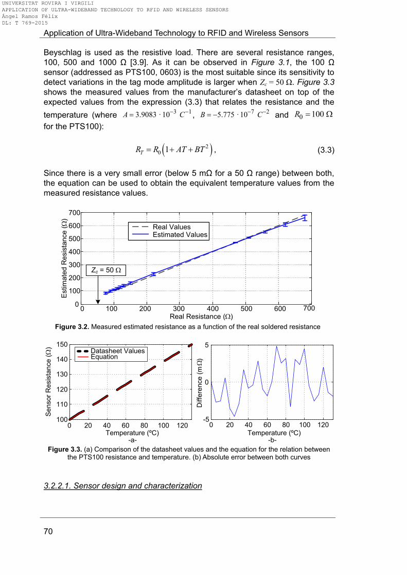
Application of Ultra-Wideband Technology to RFID and Wireless Sensors
70
Beyschlag is used as the resistive load. There are several resistance ranges,
100, 500 and 1000 Ω [3.9]. As it can be observed in Figure 3.1, the 100 Ω
sensor (addressed as PTS100, 0603) is the most suitable since its sensitivity to
detect variations in the tag mode amplitude is larger when Zc = 50 Ω. Figure 3.3
shows the measured values from the manufacturer’s datasheet on top of the
expected values from the expression (3.3) that relates the resistance and the
temperature (where 3 13.9083 · 10 A C ,
7 25.775 · 10 B C and 0 100 R
for the PTS100):
20 1TR R AT BT , (3.3)
Since there is a very small error (below 5 mΩ for a 50 Ω range) between both,
the equation can be used to obtain the equivalent temperature values from the
measured resistance values.
0 100 200 300 400 500 600 7000
100
200
300
400
500
600
700
Real Resistance ()
Estim
ate
d R
esis
tance (
)
Real ValuesEstimated Values
Zc = 50
Figure 3.2. Measured estimated resistance as a function of the real soldered resistance
0 20 40 60 80 100 120100
110
120
130
140
150
Temperature (ºC)
Sen
so
r R
esis
tance (
)
0 20 40 60 80 100 120
-5
0
5
Temperature (ºC)
Diffe
rence (
m
)
Datasheet ValuesEquation
-a- -b- Figure 3.3. (a) Comparison of the datasheet values and the equation for the relation between
the PTS100 resistance and temperature. (b) Absolute error between both curves
3.2.2.1. Sensor design and characterization
UNIVERSITAT ROVIRA I VIRGILI APPLICATION OF ULTRA-WIDEBAND TECHNOLOGY TO RFID AND WIRELESS SENSORS Ángel Ramos Félix DL: T 769-2015
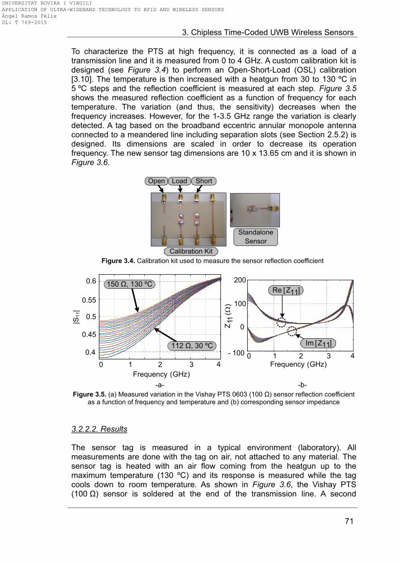
3. Chipless Time-Coded UWB Wireless Sensors
71
To characterize the PTS at high frequency, it is connected as a load of a transmission line and it is measured from 0 to 4 GHz. A custom calibration kit is designed (see Figure 3.4) to perform an Open-Short-Load (OSL) calibration [3.10]. The temperature is then increased with a heatgun from 30 to 130 ºC in 5 ºC steps and the reflection coefficient is measured at each step. Figure 3.5 shows the measured reflection coefficient as a function of frequency for each temperature. The variation (and thus, the sensitivity) decreases when the frequency increases. However, for the 1-3.5 GHz range the variation is clearly detected. A tag based on the broadband eccentric annular monopole antenna connected to a meandered line including separation slots (see Section 2.5.2) is designed. Its dimensions are scaled in order to decrease its operation frequency. The new sensor tag dimensions are 10 x 13.65 cm and it is shown in Figure 3.6.
Calibration Kit
Open Load Short
Standalone
Sensor
Figure 3.4. Calibration kit used to measure the sensor reflection coefficient
150 Ω, 130 ºC
0 1 2 3 4Frequency (GHz)
- 100
0
100
200
Z11
(
)
Im [Z ]
Re [Z11]
112 Ω, 30 ºC 11
0 1 2 3 4
Frequency (GHz)
|S11|
0.4
0.6
0.55
0.5
0.45
-a- -b- Figure 3.5. (a) Measured variation in the Vishay PTS 0603 (100 Ω) sensor reflection coefficient
as a function of frequency and temperature and (b) corresponding sensor impedance
3.2.2.2. Results The sensor tag is measured in a typical environment (laboratory). All measurements are done with the tag on air, not attached to any material. The sensor tag is heated with an air flow coming from the heatgun up to the maximum temperature (130 ºC) and its response is measured while the tag cools down to room temperature. As shown in Figure 3.6, the Vishay PTS (100 Ω) sensor is soldered at the end of the transmission line. A second
UNIVERSITAT ROVIRA I VIRGILI APPLICATION OF ULTRA-WIDEBAND TECHNOLOGY TO RFID AND WIRELESS SENSORS Ángel Ramos Félix DL: T 769-2015
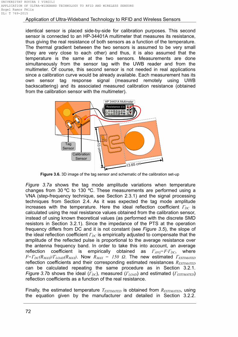
Application of Ultra-Wideband Technology to RFID and Wireless Sensors
72
identical sensor is placed side-by-side for calibration purposes. This second sensor is connected to an HP-34401A multimeter that measures its resistance, thus giving the real resistance of both sensors as a function of the temperature. The thermal gradient between the two sensors is assumed to be very small (they are very close to each other) and thus, it is also assumed that the temperature is the same at the two sensors. Measurements are done simultaneously from the sensor tag with the UWB reader and from the multimeter. Of course, this second sensor is not needed in real applications since a calibration curve would be already available. Each measurement has its own sensor tag response signal (measured remotely using UWB backscattering) and its associated measured calibration resistance (obtained from the calibration sensor with the multimeter).
Figure 3.6. 3D image of the tag sensor and schematic of the calibration set-up
Figure 3.7a shows the tag mode amplitude variations when temperature changes from 30 ºC to 130 ºC. These measurements are performed using a VNA (step-frequency technique, see Section 2.3.1) and the signal processing techniques from Section 2.4. As it was expected the tag mode amplitude increases with the temperature. Here the ideal reflection coefficient ΓDC is calculated using the real resistance values obtained from the calibration sensor, instead of using known theoretical values (as performed with the discrete SMD resistors in Section 3.2.1). Since the impedance of the PTS at the operation frequency differs from DC and it is not constant (see Figure 3.5), the slope of the ideal reflection coefficient ΓDC is empirically adjusted to compensate that the amplitude of the reflected pulse is proportional to the average resistance over the antenna frequency band. In order to take this into account, an average reflection coefficient is empirically obtained as ΓAVG=F·ΓDC, where F=ΓDC(RMAX)/ΓLOAD(RMAX). Now RMAX = 150 Ω. The new estimated ΓESTIMATED reflection coefficients and their corresponding estimated resistances RESTIMATED can be calculated repeating the same procedure as in Section 3.2.1. Figure 3.7b shows the ideal (ΓDC), measured (ΓLOAD) and estimated (ΓESTIMATED) reflection coefficients as a function of the real resistance. Finally, the estimated temperature TESTIMATED is obtained from RESTIMATED, using the equation given by the manufacturer and detailed in Section 3.2.2.
UNIVERSITAT ROVIRA I VIRGILI APPLICATION OF ULTRA-WIDEBAND TECHNOLOGY TO RFID AND WIRELESS SENSORS Ángel Ramos Félix DL: T 769-2015
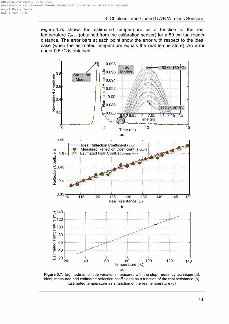
3. Chipless Time-Coded UWB Wireless Sensors
73
Figure 3.7c shows the estimated temperature as a function of the real temperature TREAL (obtained from the calibration sensor) for a 50 cm tag-reader distance. The error bars at each point show the error with respect to the ideal case (when the estimated temperature equals the real temperature). An error under 0.6 ºC is obtained.
0 5 10 150
0.2
0.4
0.6
0.8
1
Time (ns)
Norm
aliz
ed
Am
plit
ud
e
6.9 6.95 7 7.05 7.1 7.15 7.20.086
0.088
0.09
0.092
0.094
0.096
0.098
Time (ns)
No
rma
lize
d A
mp
litud
e
Structural
Modes
Tag
Modes150 , 130 ºC
112 , 30 ºC
-a-
110 115 120 125 130 135 140 145 1500.35
0.4
0.45
0.5
0.55
Real Resistance ()
Refle
ction C
oeffic
ient
Ideal Reflection Coefficient (DC)Measured Reflection Coefficient (LOAD)Estimated Refl. Coeff. (ESTIMATED)
-b-
20 40 60 80 100 120 14020
40
60
80
100
120
140
Temperature (ºC)
Estim
ate
d T
em
pe
ratu
re (
ºC)
-c-
Figure 3.7. Tag mode amplitude variations measured with the step-frequency technique (a). Ideal, measured and estimated reflection coefficients as a function of the real resistance (b).
Estimated temperature as a function of the real temperature (c)
UNIVERSITAT ROVIRA I VIRGILI APPLICATION OF ULTRA-WIDEBAND TECHNOLOGY TO RFID AND WIRELESS SENSORS Ángel Ramos Félix DL: T 769-2015
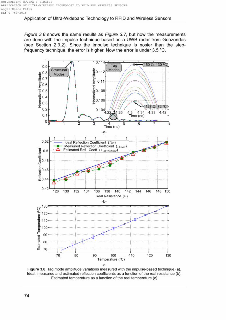
Application of Ultra-Wideband Technology to RFID and Wireless Sensors
74
Figure 3.8 shows the same results as Figure 3.7, but now the measurements are done with the impulse technique based on a UWB radar from Geozondas (see Section 2.3.2). Since the impulse technique is nosier than the step-frequency technique, the error is higher. Now the error is under 3.5 ºC.
0 1 2 3 4 5 6 7 80
0.1
0.2
0.3
0.4
0.5
0.6
0.7
0.8
0.9
1
Time (ns)
Norm
aliz
ed A
mplit
ud
e
4.22 4.26 4.3 4.34 4.38 4.420.104
0.106
0.108
0.11
0.112
0.114
Time (ns)
No
rmaliz
ed A
mp
litu
de
127 , 72 ºC
Structural
Modes
Tag
Modes
150 , 130 ºC
-a-
128 130 132 134 136 138 140 142 144 146 148 1500.42
0.44
0.46
0.48
0.5
0.52
Re
flectio
n C
oe
ffic
ien
t
Real Resistance ()
Ideal Reflection Coefficient (DC)Measured Reflection Coefficient (LOAD)
Estimated Refl . Coeff. ( ESTIMATED)
-b-
70 80 90 100 110 120 130
70
80
90
100
110
120
130
Temperature (ºC)
Estim
ate
d T
em
pe
ratu
re (
ºC)
-c-
Figure 3.8. Tag mode amplitude variations measured with the impulse-based technique (a). Ideal, measured and estimated reflection coefficients as a function of the real resistance (b).
Estimated temperature as a function of the real temperature (c)
UNIVERSITAT ROVIRA I VIRGILI APPLICATION OF ULTRA-WIDEBAND TECHNOLOGY TO RFID AND WIRELESS SENSORS Ángel Ramos Félix DL: T 769-2015
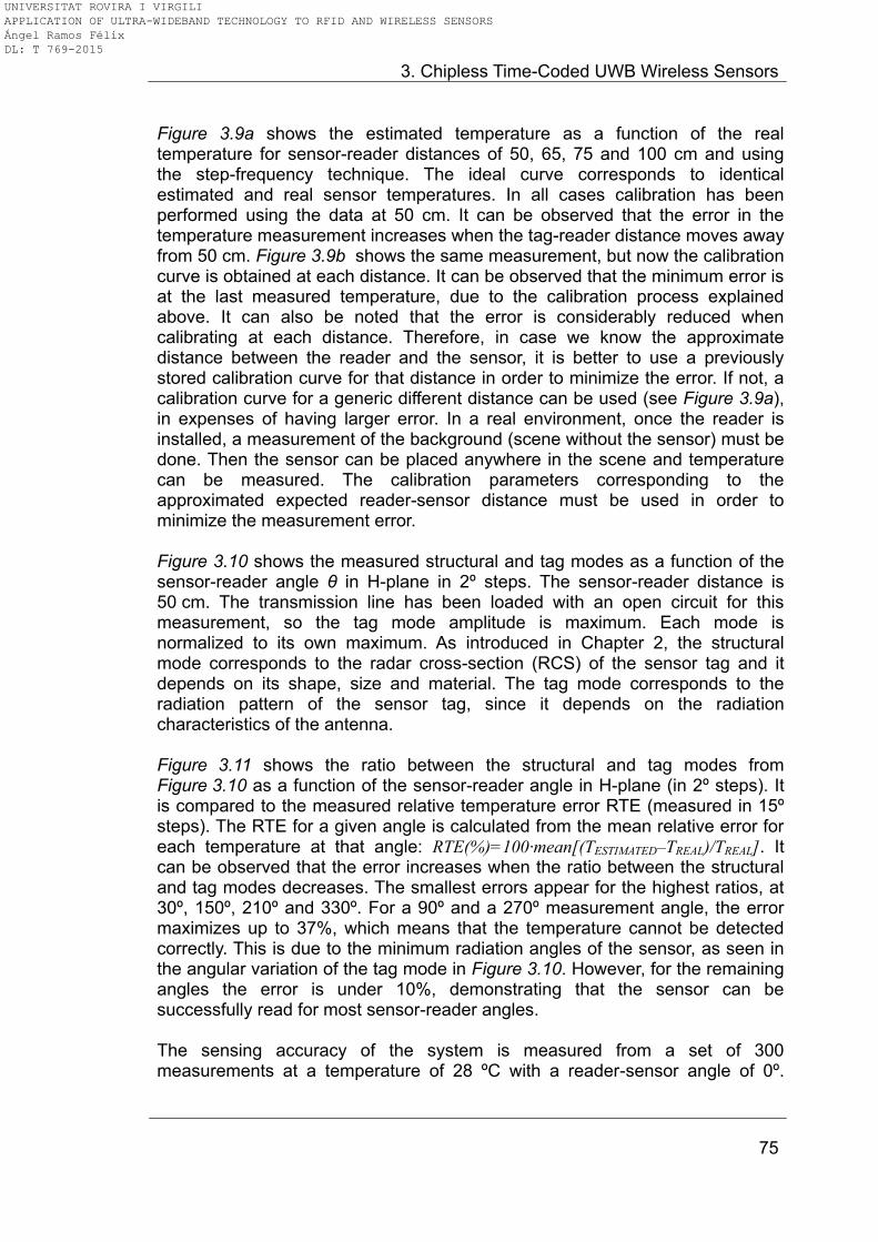
3. Chipless Time-Coded UWB Wireless Sensors
75
Figure 3.9a shows the estimated temperature as a function of the real temperature for sensor-reader distances of 50, 65, 75 and 100 cm and using the step-frequency technique. The ideal curve corresponds to identical estimated and real sensor temperatures. In all cases calibration has been performed using the data at 50 cm. It can be observed that the error in the temperature measurement increases when the tag-reader distance moves away from 50 cm. Figure 3.9b shows the same measurement, but now the calibration curve is obtained at each distance. It can be observed that the minimum error is at the last measured temperature, due to the calibration process explained above. It can also be noted that the error is considerably reduced when calibrating at each distance. Therefore, in case we know the approximate distance between the reader and the sensor, it is better to use a previously stored calibration curve for that distance in order to minimize the error. If not, a calibration curve for a generic different distance can be used (see Figure 3.9a), in expenses of having larger error. In a real environment, once the reader is installed, a measurement of the background (scene without the sensor) must be done. Then the sensor can be placed anywhere in the scene and temperature can be measured. The calibration parameters corresponding to the approximated expected reader-sensor distance must be used in order to minimize the measurement error. Figure 3.10 shows the measured structural and tag modes as a function of the sensor-reader angle θ in H-plane in 2º steps. The sensor-reader distance is 50 cm. The transmission line has been loaded with an open circuit for this measurement, so the tag mode amplitude is maximum. Each mode is normalized to its own maximum. As introduced in Chapter 2, the structural mode corresponds to the radar cross-section (RCS) of the sensor tag and it depends on its shape, size and material. The tag mode corresponds to the radiation pattern of the sensor tag, since it depends on the radiation characteristics of the antenna. Figure 3.11 shows the ratio between the structural and tag modes from Figure 3.10 as a function of the sensor-reader angle in H-plane (in 2º steps). It is compared to the measured relative temperature error RTE (measured in 15º steps). The RTE for a given angle is calculated from the mean relative error for each temperature at that angle: RTE(%)=100·mean[(TESTIMATED–TREAL)/TREAL]. It can be observed that the error increases when the ratio between the structural and tag modes decreases. The smallest errors appear for the highest ratios, at 30º, 150º, 210º and 330º. For a 90º and a 270º measurement angle, the error maximizes up to 37%, which means that the temperature cannot be detected correctly. This is due to the minimum radiation angles of the sensor, as seen in the angular variation of the tag mode in Figure 3.10. However, for the remaining angles the error is under 10%, demonstrating that the sensor can be successfully read for most sensor-reader angles. The sensing accuracy of the system is measured from a set of 300 measurements at a temperature of 28 ºC with a reader-sensor angle of 0º.
UNIVERSITAT ROVIRA I VIRGILI APPLICATION OF ULTRA-WIDEBAND TECHNOLOGY TO RFID AND WIRELESS SENSORS Ángel Ramos Félix DL: T 769-2015
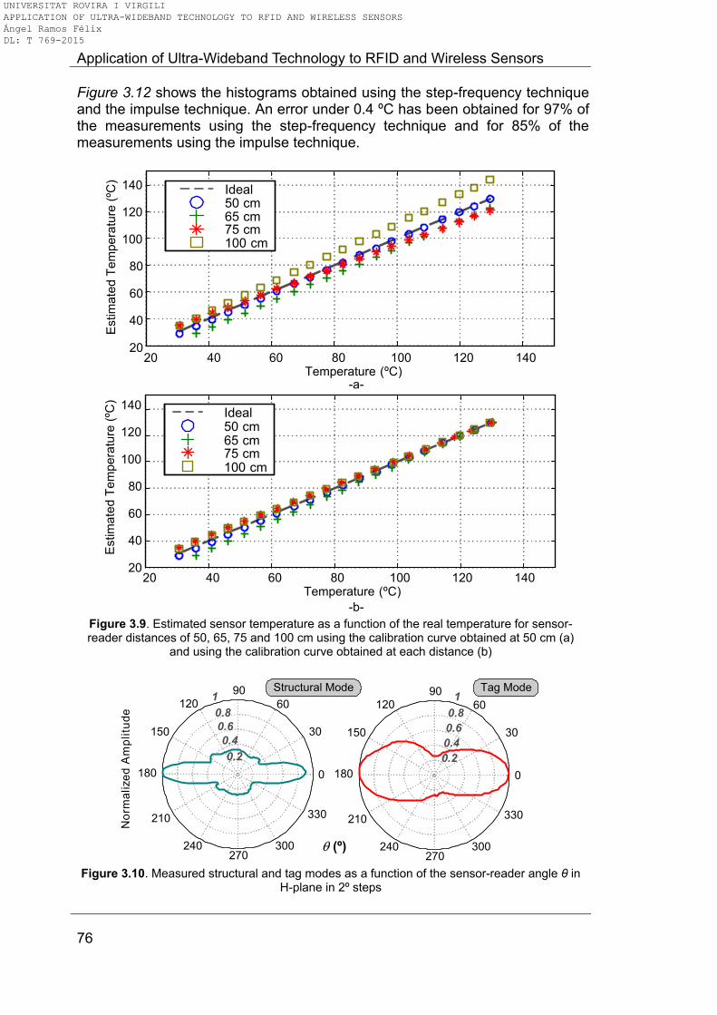
Application of Ultra-Wideband Technology to RFID and Wireless Sensors
76
Figure 3.12 shows the histograms obtained using the step-frequency technique and the impulse technique. An error under 0.4 ºC has been obtained for 97% of the measurements using the step-frequency technique and for 85% of the measurements using the impulse technique.
20 40 60 80 100 120 14020
40
60
80
100
120
140
Temperature (ºC)
Estim
ate
d T
em
pe
ratu
re (
ºC)
Ideal50 cm65 cm75 cm100 cm
Ideal50 cm65 cm75 cm100 cm
20 40 60 80 100 120 14020
40
60
80
100
120
140
Temperature (ºC)
Estim
ate
d T
em
pe
ratu
re (
ºC)
-a-
-b- Figure 3.9. Estimated sensor temperature as a function of the real temperature for sensor-reader distances of 50, 65, 75 and 100 cm using the calibration curve obtained at 50 cm (a)
and using the calibration curve obtained at each distance (b)
0.2
0.4
0.6
0.8
1
30
210
60
240
90
270
120
300
150
330
180 0
0.2
0.4
0.6
0.8
1
30
210
60
240
90
270
120
300
150
330
180 0
(º)
No
rma
lize
d A
mp
litu
de
Structural Mode Tag Mode
Figure 3.10. Measured structural and tag modes as a function of the sensor-reader angle θ in
H-plane in 2º steps
UNIVERSITAT ROVIRA I VIRGILI APPLICATION OF ULTRA-WIDEBAND TECHNOLOGY TO RFID AND WIRELESS SENSORS Ángel Ramos Félix DL: T 769-2015
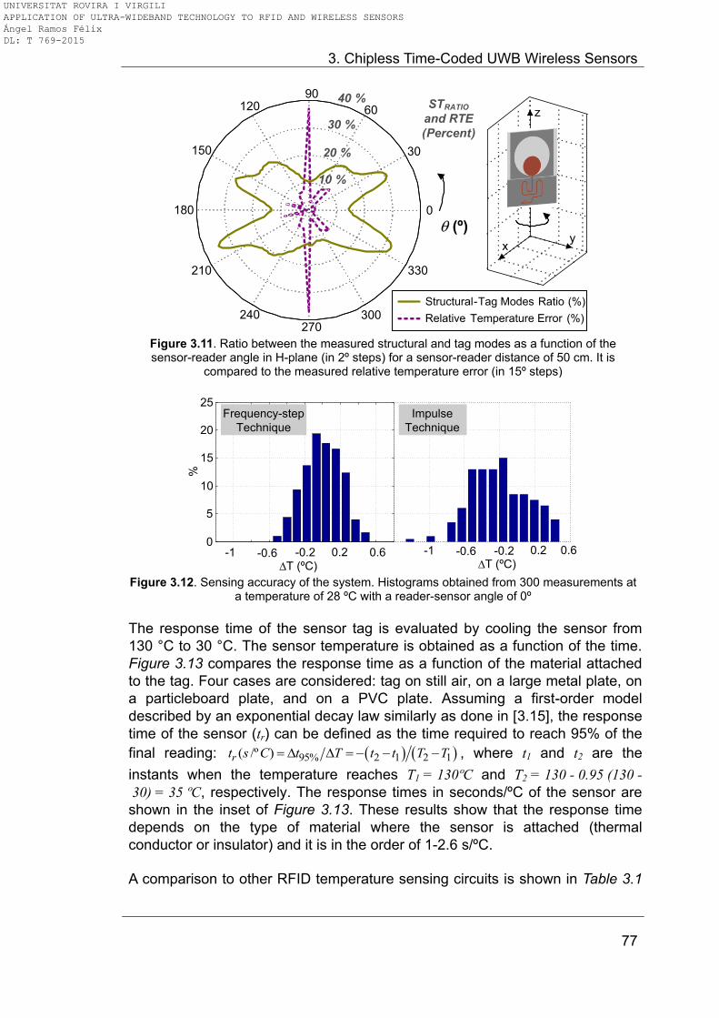
3. Chipless Time-Coded UWB Wireless Sensors
77
10 %
20 %
30 %
40 %
30
210
60
240
90
270
120
300
150
330
180 0
Structural-Tag Modes Ratio (%)
Relative Temperature Error (%)
xy
z
(º)
STRATIO
and RTE
(Percent)
Figure 3.11. Ratio between the measured structural and tag modes as a function of the sensor-reader angle in H-plane (in 2º steps) for a sensor-reader distance of 50 cm. It is
compared to the measured relative temperature error (in 15º steps)
-1 -0.6 -0.2 0.2 0.60
5
10
15
20
25
T (ºC)
%
-1 -0.6 -0.2 0.2 0.6
T (ºC)
Frequency-step
Technique
Impulse
Technique
Figure 3.12. Sensing accuracy of the system. Histograms obtained from 300 measurements at
a temperature of 28 ºC with a reader-sensor angle of 0º
The response time of the sensor tag is evaluated by cooling the sensor from
130 °C to 30 °C. The sensor temperature is obtained as a function of the time.
Figure 3.13 compares the response time as a function of the material attached
to the tag. Four cases are considered: tag on still air, on a large metal plate, on
a particleboard plate, and on a PVC plate. Assuming a first-order model
described by an exponential decay law similarly as done in [3.15], the response
time of the sensor (tr) can be defined as the time required to reach 95% of the
final reading: 95% 2 1 2 1( /º )rt s C t T t t T T , where t1 and t2 are the
instants when the temperature reaches T1 = 130ºC and T2 = 130 - 0.95 (130 -
30) = 35 ºC, respectively. The response times in seconds/ºC of the sensor are
shown in the inset of Figure 3.13. These results show that the response time
depends on the type of material where the sensor is attached (thermal
conductor or insulator) and it is in the order of 1-2.6 s/ºC.
A comparison to other RFID temperature sensing circuits is shown in Table 3.1
UNIVERSITAT ROVIRA I VIRGILI APPLICATION OF ULTRA-WIDEBAND TECHNOLOGY TO RFID AND WIRELESS SENSORS Ángel Ramos Félix DL: T 769-2015
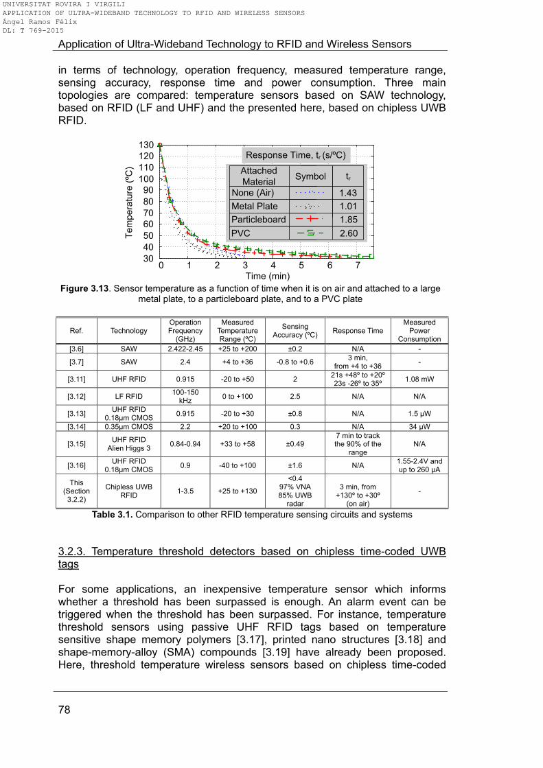
Application of Ultra-Wideband Technology to RFID and Wireless Sensors
78
in terms of technology, operation frequency, measured temperature range, sensing accuracy, response time and power consumption. Three main topologies are compared: temperature sensors based on SAW technology, based on RFID (LF and UHF) and the presented here, based on chipless UWB RFID.
0 1 2 3 4 5 6 730
40
50
60
70
80
90
100
110
120
130
Time (min)
Tem
pera
ture
(ºC
)
Response Time, tr (s/ºC)
Attached
MaterialSymbol tr
None (Air)
Metal Plate
Particleboard
PVC
1.43
1.01
1.85
2.60
Figure 3.13. Sensor temperature as a function of time when it is on air and attached to a large
metal plate, to a particleboard plate, and to a PVC plate
Ref. Technology Operation Frequency
(GHz)
Measured Temperature Range (ºC)
Sensing Accuracy (ºC)
Response Time Measured
Power Consumption
[3.6] SAW 2.422-2.45 +25 to +200 ±0.2 N/A -
[3.7] SAW 2.4 +4 to +36 -0.8 to +0.6 3 min,
from +4 to +36 -
[3.11] UHF RFID 0.915 -20 to +50 2 21s +48º to +20º 23s -26º to 35º
1.08 mW
[3.12] LF RFID 100-150
kHz 0 to +100 2.5 N/A N/A
[3.13] UHF RFID
0.18μm CMOS 0.915 -20 to +30 ±0.8 N/A 1.5 μW
[3.14] 0.35μm CMOS 2.2 +20 to +100 0.3 N/A 34 μW
[3.15] UHF RFID
Alien Higgs 3 0.84-0.94 +33 to +58 ±0.49
7 min to track the 90% of the
range N/A
[3.16] UHF RFID
0.18μm CMOS 0.9 -40 to +100 ±1.6 N/A
1.55-2.4V and up to 260 μA
This (Section
3.2.2)
Chipless UWB RFID
1-3.5 +25 to +130
<0.4 97% VNA 85% UWB
radar
3 min, from
+130º to +30º (on air)
-
Table 3.1. Comparison to other RFID temperature sensing circuits and systems
3.2.3. Temperature threshold detectors based on chipless time-coded UWB tags For some applications, an inexpensive temperature sensor which informs whether a threshold has been surpassed is enough. An alarm event can be triggered when the threshold has been surpassed. For instance, temperature threshold sensors using passive UHF RFID tags based on temperature sensitive shape memory polymers [3.17], printed nano structures [3.18] and shape-memory-alloy (SMA) compounds [3.19] have already been proposed. Here, threshold temperature wireless sensors based on chipless time-coded
UNIVERSITAT ROVIRA I VIRGILI APPLICATION OF ULTRA-WIDEBAND TECHNOLOGY TO RFID AND WIRELESS SENSORS Ángel Ramos Félix DL: T 769-2015
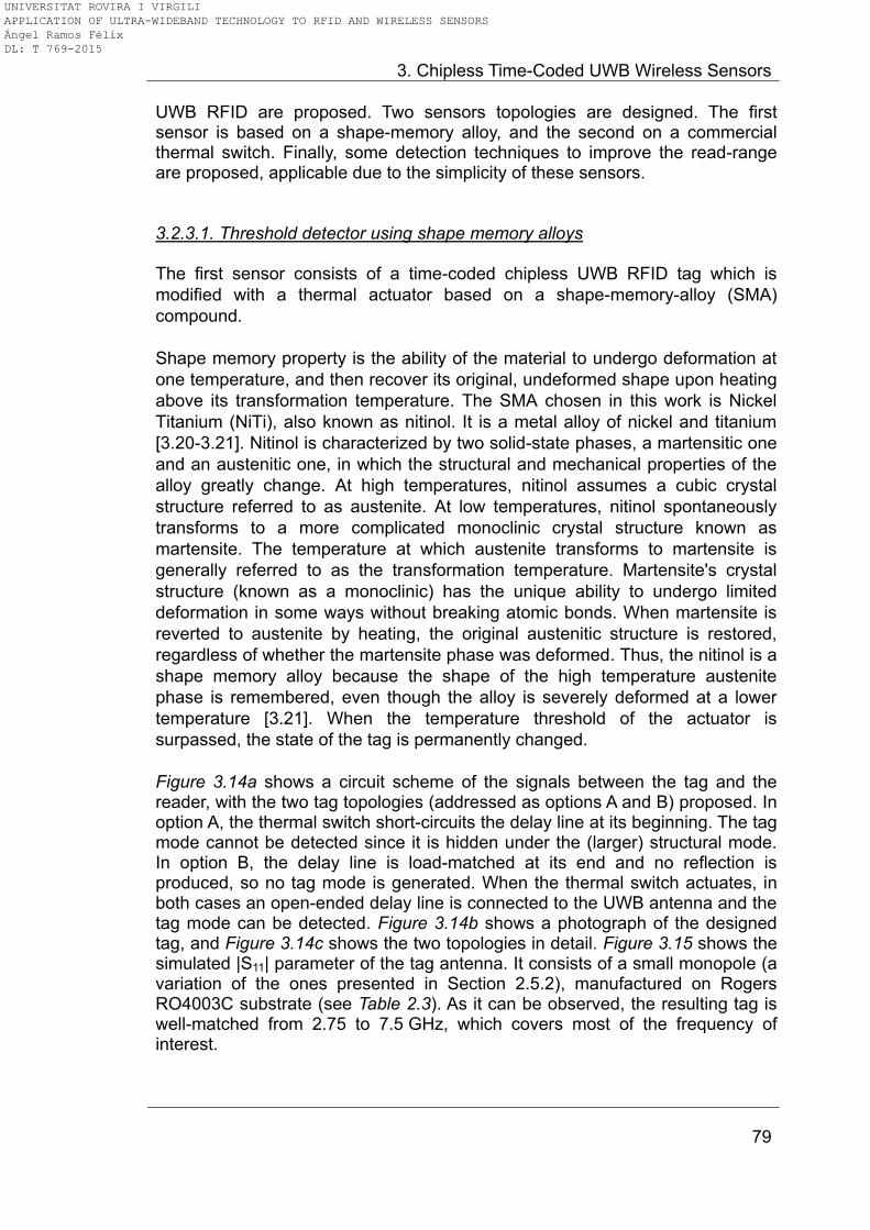
3. Chipless Time-Coded UWB Wireless Sensors
79
UWB RFID are proposed. Two sensors topologies are designed. The first sensor is based on a shape-memory alloy, and the second on a commercial thermal switch. Finally, some detection techniques to improve the read-range are proposed, applicable due to the simplicity of these sensors. 3.2.3.1. Threshold detector using shape memory alloys The first sensor consists of a time-coded chipless UWB RFID tag which is
modified with a thermal actuator based on a shape-memory-alloy (SMA)
compound.
Shape memory property is the ability of the material to undergo deformation at
one temperature, and then recover its original, undeformed shape upon heating
above its transformation temperature. The SMA chosen in this work is Nickel
Titanium (NiTi), also known as nitinol. It is a metal alloy of nickel and titanium
[3.20-3.21]. Nitinol is characterized by two solid-state phases, a martensitic one
and an austenitic one, in which the structural and mechanical properties of the
alloy greatly change. At high temperatures, nitinol assumes a cubic crystal
structure referred to as austenite. At low temperatures, nitinol spontaneously
transforms to a more complicated monoclinic crystal structure known as
martensite. The temperature at which austenite transforms to martensite is
generally referred to as the transformation temperature. Martensite's crystal
structure (known as a monoclinic) has the unique ability to undergo limited
deformation in some ways without breaking atomic bonds. When martensite is
reverted to austenite by heating, the original austenitic structure is restored,
regardless of whether the martensite phase was deformed. Thus, the nitinol is a
shape memory alloy because the shape of the high temperature austenite
phase is remembered, even though the alloy is severely deformed at a lower
temperature [3.21]. When the temperature threshold of the actuator is
surpassed, the state of the tag is permanently changed.
Figure 3.14a shows a circuit scheme of the signals between the tag and the reader, with the two tag topologies (addressed as options A and B) proposed. In option A, the thermal switch short-circuits the delay line at its beginning. The tag mode cannot be detected since it is hidden under the (larger) structural mode. In option B, the delay line is load-matched at its end and no reflection is produced, so no tag mode is generated. When the thermal switch actuates, in both cases an open-ended delay line is connected to the UWB antenna and the tag mode can be detected. Figure 3.14b shows a photograph of the designed tag, and Figure 3.14c shows the two topologies in detail. Figure 3.15 shows the simulated |S11| parameter of the tag antenna. It consists of a small monopole (a variation of the ones presented in Section 2.5.2), manufactured on Rogers RO4003C substrate (see Table 2.3). As it can be observed, the resulting tag is well-matched from 2.75 to 7.5 GHz, which covers most of the frequency of interest.
UNIVERSITAT ROVIRA I VIRGILI APPLICATION OF ULTRA-WIDEBAND TECHNOLOGY TO RFID AND WIRELESS SENSORS Ángel Ramos Félix DL: T 769-2015
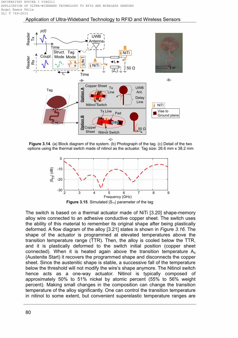
Application of Ultra-Wideband Technology to RFID and Wireless Sensors
80
UWB
Antenna
(Zc)
L
Time
Struct.
Mode
Time
p(t)
τL
Tag
ModeCoupl.
Rea
der
Tx
NiTi50 Ω
A
B
NiT
i
NiTi
Rea
der
Rx
-a-
-b-
Copper SheetTx
Line
50 Ω
Tx Line
Copper
Sheet
Pad
Op
tio
n B
Op
tio
n A
Nitinol Switch
Nitinol Switch
UWB
Ant.
Delay
Line
50 Ω
Vias to
Ground plane
NiTi
Tag
-c-
Figure 3.14. (a) Block diagram of the system. (b) Photograph of the tag. (c) Detail of the two options using the thermal switch made of nitinol as the actuator. Tag size: 26.6 mm x 38.2 mm
2 3 4 5 6 7 8 9-30
-20
-10
0
Frequency (GHz)
|S11
| (d
B)
Figure 3.15. Simulated |S11| parameter of the tag
The switch is based on a thermal actuator made of NiTi [3.20] shape-memory alloy wire connected to an adhesive conductive copper sheet. The switch uses the ability of this material to remember its original shape after being plastically deformed. A flow diagram of the alloy [3.21] states is shown in Figure 3.16. The shape of the actuator is programmed at elevated temperatures above the transition temperature range (TTR). Then, the alloy is cooled below the TTR, and it is plastically deformed to the switch initial position (copper sheet connected). When it is heated again above the transition temperature As (Austenite Start) it recovers the programmed shape and disconnects the copper sheet. Since the austenitic shape is stable, a successive fall of the temperature below the threshold will not modify the wire’s shape anymore. The Nitinol switch hence acts as a one-way actuator. Nitinol is typically composed of approximately 50% to 51% nickel by atomic percent (55% to 56% weight percent). Making small changes in the composition can change the transition temperature of the alloy significantly. One can control the transition temperature in nitinol to some extent, but convenient superelastic temperature ranges are
UNIVERSITAT ROVIRA I VIRGILI APPLICATION OF ULTRA-WIDEBAND TECHNOLOGY TO RFID AND WIRELESS SENSORS Ángel Ramos Félix DL: T 769-2015
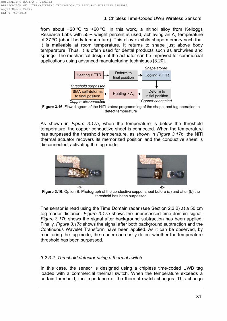
3. Chipless Time-Coded UWB Wireless Sensors
81
from about −20 °C to +60 °C. In this work, a nitinol alloy from Kelloggs Research Labs with 55% weight percent is used, achieving an As temperature of 37 ºC (about body temperature). This alloy exhibits shape memory such that it is malleable at room temperature. It returns to shape just above body temperature. Thus, it is often used for dental products such as archwires and springs. The mechanical design of the actuator can be improved for commercial applications using advanced manufacturing techniques [3.20].
Heating > TTRDeform to
final positionCooling < TTR
Heating > AsSMA self-deforms
to final position
Shape stored
Deform to
initial position
Copper connectedCopper disconnected
Threshold surpassed
Figure 3.16. Flow diagram of the NiTi states: programming of the shape, and tag operation to
detect temperature
As shown in Figure 3.17a, when the temperature is below the threshold temperature, the copper conductive sheet is connected. When the temperature has surpassed the threshold temperature, as shown in Figure 3.17b, the NiTi thermal actuator recovers its memorized position and the conductive sheet is disconnected, activating the tag mode.
-a-
-b-
Figure 3.16. Option B. Photograph of the conductive copper sheet before (a) and after (b) the threshold has been surpassed
The sensor is read using the Time Domain radar (see Section 2.3.2) at a 50 cm tag-reader distance. Figure 3.17a shows the unprocessed time-domain signal. Figure 3.17b shows the signal after background subtraction has been applied. Finally, Figure 3.17c shows the signal after both background subtraction and the Continuous Wavelet Transform have been applied. As it can be observed, by monitoring the tag mode, the reader can easily detect whether the temperature threshold has been surpassed.
3.2.3.2. Threshold detector using a thermal switch
In this case, the sensor is designed using a chipless time-coded UWB tag loaded with a commercial thermal switch. When the temperature exceeds a certain threshold, the impedance of the thermal switch changes. This change
UNIVERSITAT ROVIRA I VIRGILI APPLICATION OF ULTRA-WIDEBAND TECHNOLOGY TO RFID AND WIRELESS SENSORS Ángel Ramos Félix DL: T 769-2015
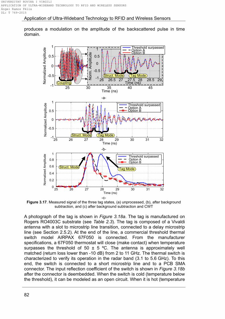
Application of Ultra-Wideband Technology to RFID and Wireless Sensors
82
produces a modulation on the amplitude of the backscattered pulse in time domain.
25 30 35 40 45-1
-0.5
0
0.5
1
Time (ns)
Norm
aliz
ed
Am
plit
ud
e
26 26.5 27 27.5 28 28.5 29-1
-0.5
0
0.5
1
Time (ns)
Norm
. A
mplit
ude
Threshold surpassedOption AOption B
Coupling
Struct. Mode Tag Mode
-a-
25 26 27 28 29 30 31 32-1
-0.5
0
0.5
1
Time (ns)
Norm
aliz
ed A
mplit
ude
Threshold surpassedOption AOption B
Struct. Mode Tag Mode
-b-
25 26 27 28 29 30 31 320
0.2
0.4
0.6
0.8
1
Time (ns)
Norm
aliz
ed A
mplit
ude
Threshold surpassedOption AOption B
Struct. ModeTag Mode
-c-
Figure 3.17. Measured signal of the three tag states, (a) unprocessed, (b), after background subtraction, and (c) after background subtraction and CWT
A photograph of the tag is shown in Figure 3.18a. The tag is manufactured on Rogers RO4003C substrate (see Table 2.3). The tag is composed of a Vivaldi antenna with a slot to microstrip line transition, connected to a delay microstrip line (see Section 2.5.2). At the end of the line, a commercial threshold thermal switch model AIRPAX 67F050 is connected. From the manufacturer specifications, a 67F050 thermostat will close (make contact) when temperature surpasses the threshold of 50 ± 5 ºC. The antenna is approximately well matched (return loss lower than -10 dB) from 2 to 11 GHz. The thermal switch is characterized to verify its operation in the radar band (3.1 to 5.6 GHz). To this end, the switch is connected to a short microstrip line and to a PCB SMA connector. The input reflection coefficient of the switch is shown in Figure 3.18b after the connector is deembedded. When the switch is cold (temperature below the threshold), it can be modeled as an open circuit. When it is hot (temperature
UNIVERSITAT ROVIRA I VIRGILI APPLICATION OF ULTRA-WIDEBAND TECHNOLOGY TO RFID AND WIRELESS SENSORS Ángel Ramos Félix DL: T 769-2015
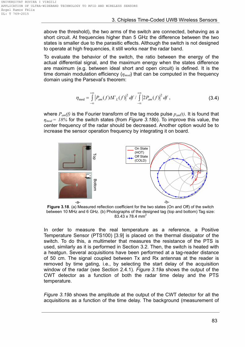
3. Chipless Time-Coded UWB Wireless Sensors
83
above the threshold), the two arms of the switch are connected, behaving as a short circuit. At frequencies higher than 5 GHz the difference between the two states is smaller due to the parasitic effects. Although the switch is not designed to operate at high frequencies, it still works near the radar band.
To evaluate the behavior of the switch, the ratio between the energy of the actual differential signal, and the maximum energy when the states difference are maximum (e.g. between ideal short and open circuit) is defined. It is the time domain modulation efficiency (ηmod) that can be computed in the frequency domain using the Parseval’s theorem:
2 2
mod ( ) ( ) / 2 ( )am L amP f f df P f df
, (3.4)
where Pam(f) is the Fourier transform of the tag mode pulse pam(t). It is found that ηmod = 18% for the switch states (from Figure 3.18b). To improve this value, the center frequency of the radar should be decreased. Another option would be to increase the sensor operation frequency by integrating it on board.
-a-
On State
(HOT)
Off State
(COLD)
-b-
Figure 3.18. (a) Measured reflection coefficient for the two states (On and Off) of the switch between 10 MHz and 6 GHz. (b) Photographs of the designed tag (top and bottom) Tag size:
83.43 x 78.4 mm2
In order to measure the real temperature as a reference, a Positive Temperature Sensor (PTS100) [3.9] is placed on the thermal dissipator of the switch. To do this, a multimeter that measures the resistance of the PTS is used, similarly as it is performed in Section 3.2. Then, the switch is heated with a heatgun. Several acquisitions have been performed at a tag-reader distance of 50 cm. The signal coupled between Tx and Rx antennas at the reader is removed by time gating, i.e., by selecting the start delay of the acquisition window of the radar (see Section 2.4.1). Figure 3.19a shows the output of the CWT detector as a function of both the radar time delay and the PTS temperature.
Figure 3.19b shows the amplitude at the output of the CWT detector for all the acquisitions as a function of the time delay. The background (measurement of
Top
Botto
m
UNIVERSITAT ROVIRA I VIRGILI APPLICATION OF ULTRA-WIDEBAND TECHNOLOGY TO RFID AND WIRELESS SENSORS Ángel Ramos Félix DL: T 769-2015
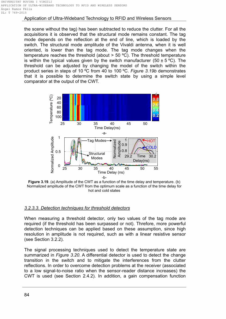
Application of Ultra-Wideband Technology to RFID and Wireless Sensors
84
the scene without the tag) has been subtracted to reduce the clutter. For all the acquisitions it is observed that the structural mode remains constant. The tag mode depends on the reflection at the end of line, which is loaded by the switch. The structural mode amplitude of the Vivaldi antenna, when it is well oriented, is lower than the tag mode. The tag mode changes when the temperature reaches the threshold (about > 50 ºC). The threshold temperature is within the typical values given by the switch manufacturer (50 ± 5 ºC). The threshold can be adjusted by changing the model of the switch within the product series in steps of 10 ºC from 40 to 100 ºC. Figure 3.19b demonstrates that it is possible to determine the switch state by using a simple level comparator at the output of the CWT.
Time Delay(ns)
Tem
pera
ture
(ºC
)
25 30 35 40 45 50
20
40
60
80
100 0.20.20.40.4
0.60.60.80.811
-a-
25 30 35 40 45 50 550
0.5
1
No
rma
lize
d A
mp
litu
de
Time Delay (ns)
29.2 30.2
0.8
0.9
1
No
rma
lize
d
Am
plit
ud
e
Time
Delay(ns)
Tag Modes HOT
COLD
Structural
Modes
-b-
Figure 3.19. (a) Amplitude of the CWT as a function of the time delay and temperature. (b) Normalized amplitude of the CWT from the optimum scale as a function of the time delay for
hot and cold states
3.2.3.3. Detection techniques for threshold detectors When measuring a threshold detector, only two values of the tag mode are required (if the threshold has been surpassed or not). Threfore, more powerful detection techniques can be applied based on these assumption, since high resolution in amplitude is not required, such as with a linear resistive sensor (see Section 3.2.2). The signal processing techniques used to detect the temperature state are summarized in Figure 3.20. A differential detector is used to detect the change transition in the switch and to mitigate the interferences from the clutter reflections. In order to overcome detection problems at the receiver (associated to a low signal-to-noise ratio when the sensor-reader distance increases) the CWT is used (see Section 2.4.2). In addition, a gain compensation function
UNIVERSITAT ROVIRA I VIRGILI APPLICATION OF ULTRA-WIDEBAND TECHNOLOGY TO RFID AND WIRELESS SENSORS Ángel Ramos Félix DL: T 769-2015
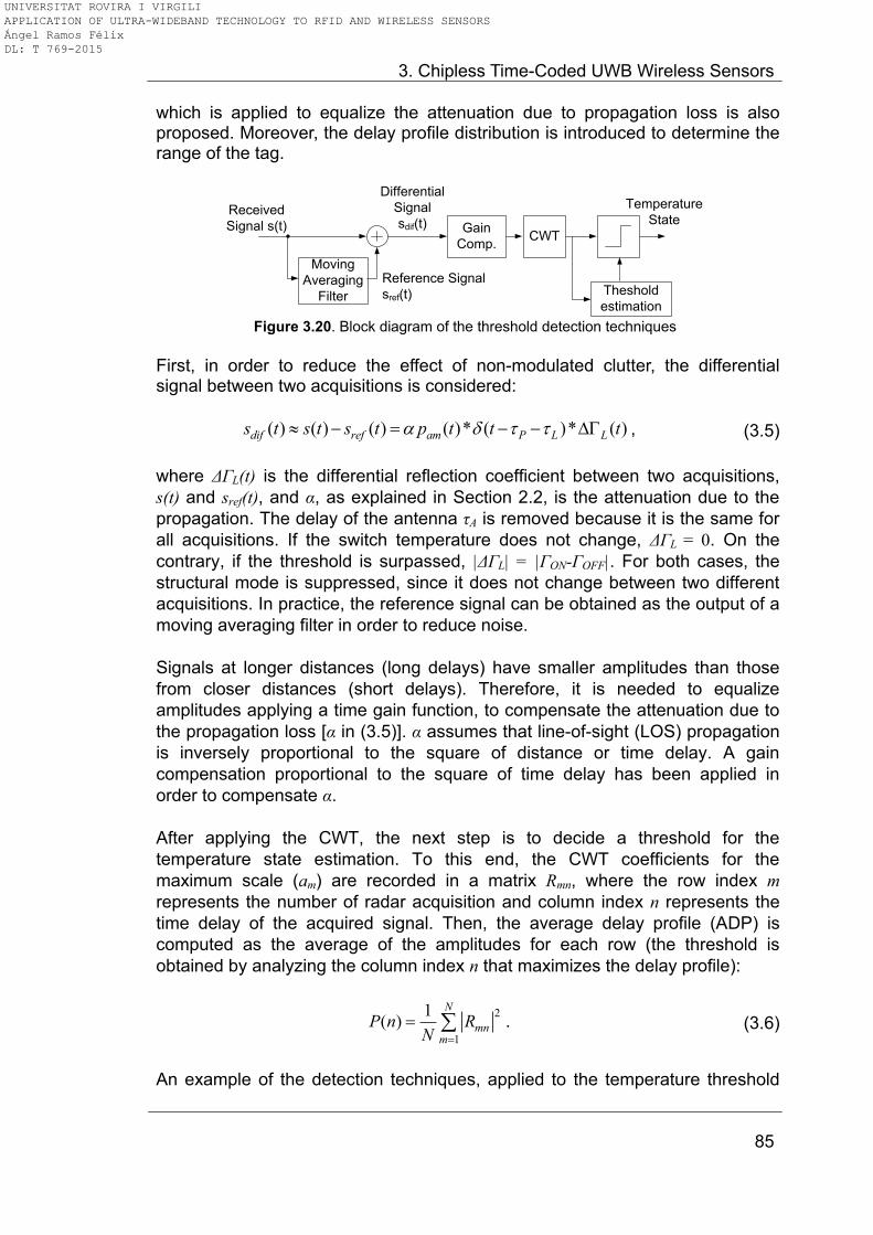
3. Chipless Time-Coded UWB Wireless Sensors
85
which is applied to equalize the attenuation due to propagation loss is also proposed. Moreover, the delay profile distribution is introduced to determine the range of the tag.
Received
Signal s(t)
Moving
Averaging
Filter
Reference Signal
sref(t)
Differential
Signal
sdif(t)CWT
Temperature
StateGain
Comp.
Theshold
estimation
Figure 3.20. Block diagram of the threshold detection techniques
First, in order to reduce the effect of non-modulated clutter, the differential signal between two acquisitions is considered:
( ) ( ) ( ) ( )* ( )* ( )dif ref am P L Ls t s t s t p t t t , (3.5)
where ΔΓL(t) is the differential reflection coefficient between two acquisitions,
s(t) and sref(t), and α, as explained in Section 2.2, is the attenuation due to the
propagation. The delay of the antenna ηA is removed because it is the same for
all acquisitions. If the switch temperature does not change, ΔΓL = 0. On the
contrary, if the threshold is surpassed, |ΔΓL| = |ΓON-ΓOFF|. For both cases, the
structural mode is suppressed, since it does not change between two different
acquisitions. In practice, the reference signal can be obtained as the output of a
moving averaging filter in order to reduce noise.
Signals at longer distances (long delays) have smaller amplitudes than those
from closer distances (short delays). Therefore, it is needed to equalize
amplitudes applying a time gain function, to compensate the attenuation due to
the propagation loss [α in (3.5)]. α assumes that line-of-sight (LOS) propagation
is inversely proportional to the square of distance or time delay. A gain
compensation proportional to the square of time delay has been applied in
order to compensate α.
After applying the CWT, the next step is to decide a threshold for the
temperature state estimation. To this end, the CWT coefficients for the
maximum scale (am) are recorded in a matrix Rmn, where the row index m
represents the number of radar acquisition and column index n represents the
time delay of the acquired signal. Then, the average delay profile (ADP) is
computed as the average of the amplitudes for each row (the threshold is
obtained by analyzing the column index n that maximizes the delay profile):
2
1
1( )
N
mnm
P n RN
. (3.6)
An example of the detection techniques, applied to the temperature threshold
UNIVERSITAT ROVIRA I VIRGILI APPLICATION OF ULTRA-WIDEBAND TECHNOLOGY TO RFID AND WIRELESS SENSORS Ángel Ramos Félix DL: T 769-2015

Application of Ultra-Wideband Technology to RFID and Wireless Sensors
86
detector based on a commercial thermal switch (see Section 3.2.3.2) is shown next. Figure 3.21a shows the maximum of the CWT for different acquisitions at a 5 m tag-reader distance. Figure 3.21b shows the measured signals after the gain compensation has been applied. Finally, undesired clutter is removed using sref(t), avoiding the use of the background subtraction. sref(t) is obtained by averaging the first acquisitions. This is possible because the switch is assumed to be cold when the monitorization starts, before the temperature could exceed the threshold. Then, the differential signal is obtained by subtracting each acquisition from the reference signal. Figure 3.21c shows the differential signal obtained from the gain-compensated signal from Figure 3.21b. The temperature state is obtained by comparing the output of CWT with a threshold value.
Measu
rem
ent N
um
ber -a-
20
60
100
20
60
100
Time Delay (ns)
45 50 55 60 65 70
20
60
100
0.2
0.4
0.6
0.8
-b-
-c-
Figure 3.21. Normalized amplitude of the CWT for the optimum scale before (a) and after (b) applying gain compensation. (c) Normalized amplitude of the CWT of the Differential signal.
The distance between reader and tag is 5 m
Figure 3.22a shows the average delay profile distribution (see Eq. 3.27) of the CWT, obtained from the averaging of all acquisitions for each time delay. The peak corresponds to the maximum variation of the differential signal due to the change in the antenna mode of the sensor. From the time delay of the peak, it is easy to localize the tag distance. A cut of the output of CWT for this time delay is shown in Figure 3.22b. Figure 3.22c shows the complementary distribution function (CDF) of the amplitudes of Figure 3.22b. According to this function, the threshold is fixed to the midpoint between the minimum and the maximum points. The measurements whose amplitude is higher than this threshold value correspond to hot switch states. In addition, the fraction of time when the detector is cold (TCOLD/T) can be obtained from this graphic. 3.2.4. Self-calibration and reliability
There are a number of issues that must be addressed in order to make chipless
sensors competitive in front of other alternative chip-based solutions. Some of
these aspects are the read range, the reliability, the accuracy or the sensor
calibration process.
UNIVERSITAT ROVIRA I VIRGILI APPLICATION OF ULTRA-WIDEBAND TECHNOLOGY TO RFID AND WIRELESS SENSORS Ángel Ramos Félix DL: T 769-2015
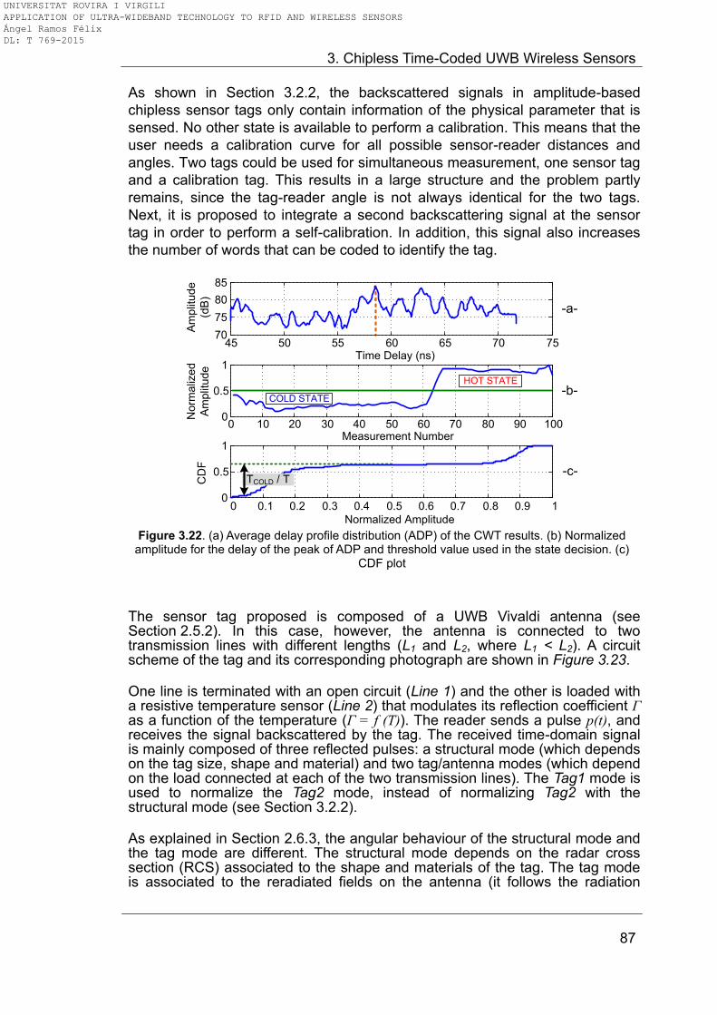
3. Chipless Time-Coded UWB Wireless Sensors
87
As shown in Section 3.2.2, the backscattered signals in amplitude-based
chipless sensor tags only contain information of the physical parameter that is
sensed. No other state is available to perform a calibration. This means that the
user needs a calibration curve for all possible sensor-reader distances and
angles. Two tags could be used for simultaneous measurement, one sensor tag
and a calibration tag. This results in a large structure and the problem partly
remains, since the tag-reader angle is not always identical for the two tags.
Next, it is proposed to integrate a second backscattering signal at the sensor
tag in order to perform a self-calibration. In addition, this signal also increases
the number of words that can be coded to identify the tag.
45 50 55 60 65 70 7570
75
80
85
Time Delay (ns)
Am
plit
ude
(dB
)
0 10 20 30 40 50 60 70 80 90 1000
0.5
1
Measurement Number
Norm
aliz
ed
Am
plit
ude
-b-HOT STATE
COLD STATE
-a-
0 0.1 0.2 0.3 0.4 0.5 0.6 0.7 0.8 0.9 10
0.5
1
Normalized Amplitude
CD
F
-c-TCOLD / T
Figure 3.22. (a) Average delay profile distribution (ADP) of the CWT results. (b) Normalized
amplitude for the delay of the peak of ADP and threshold value used in the state decision. (c) CDF plot
The sensor tag proposed is composed of a UWB Vivaldi antenna (see Section 2.5.2). In this case, however, the antenna is connected to two transmission lines with different lengths (L1 and L2, where L1 < L2). A circuit scheme of the tag and its corresponding photograph are shown in Figure 3.23.
One line is terminated with an open circuit (Line 1) and the other is loaded with a resistive temperature sensor (Line 2) that modulates its reflection coefficient Γ as a function of the temperature (Γ = f (T)). The reader sends a pulse p(t), and receives the signal backscattered by the tag. The received time-domain signal is mainly composed of three reflected pulses: a structural mode (which depends on the tag size, shape and material) and two tag/antenna modes (which depend on the load connected at each of the two transmission lines). The Tag1 mode is used to normalize the Tag2 mode, instead of normalizing Tag2 with the structural mode (see Section 3.2.2).
As explained in Section 2.6.3, the angular behaviour of the structural mode and the tag mode are different. The structural mode depends on the radar cross section (RCS) associated to the shape and materials of the tag. The tag mode is associated to the reradiated fields on the antenna (it follows the radiation
UNIVERSITAT ROVIRA I VIRGILI APPLICATION OF ULTRA-WIDEBAND TECHNOLOGY TO RFID AND WIRELESS SENSORS Ángel Ramos Félix DL: T 769-2015
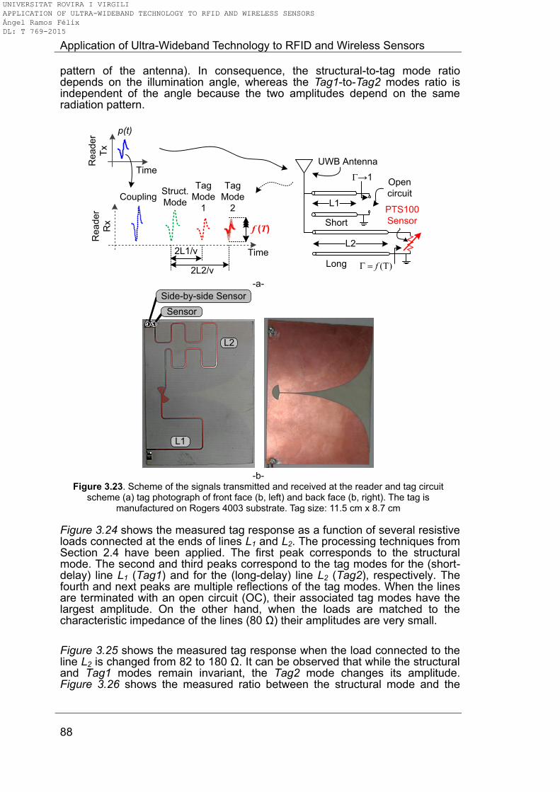
Application of Ultra-Wideband Technology to RFID and Wireless Sensors
88
pattern of the antenna). In consequence, the structural-to-tag mode ratio depends on the illumination angle, whereas the Tag1-to-Tag2 modes ratio is independent of the angle because the two amplitudes depend on the same radiation pattern.
Time
Struct.
Mode
Time
p(t)
Tag
Mode
2
2L1/v
f (T)
Rea
der
Tx
Rea
der
Rx
→1
L1
f T
L2
PTS100
Sensor
Open
circuit
UWB Antenna
Short
Long
Tag
Mode
1
2L2/v
Coupling
-a-
L1
L2
Sensor
Side-by-side Sensor
-b-
Figure 3.23. Scheme of the signals transmitted and received at the reader and tag circuit scheme (a) tag photograph of front face (b, left) and back face (b, right). The tag is
manufactured on Rogers 4003 substrate. Tag size: 11.5 cm x 8.7 cm
Figure 3.24 shows the measured tag response as a function of several resistive loads connected at the ends of lines L1 and L2. The processing techniques from Section 2.4 have been applied. The first peak corresponds to the structural mode. The second and third peaks correspond to the tag modes for the (short-delay) line L1 (Tag1) and for the (long-delay) line L2 (Tag2), respectively. The fourth and next peaks are multiple reflections of the tag modes. When the lines are terminated with an open circuit (OC), their associated tag modes have the largest amplitude. On the other hand, when the loads are matched to the characteristic impedance of the lines (80 Ω) their amplitudes are very small.
Figure 3.25 shows the measured tag response when the load connected to the line L2 is changed from 82 to 180 Ω. It can be observed that while the structural and Tag1 modes remain invariant, the Tag2 mode changes its amplitude. Figure 3.26 shows the measured ratio between the structural mode and the
UNIVERSITAT ROVIRA I VIRGILI APPLICATION OF ULTRA-WIDEBAND TECHNOLOGY TO RFID AND WIRELESS SENSORS Ángel Ramos Félix DL: T 769-2015
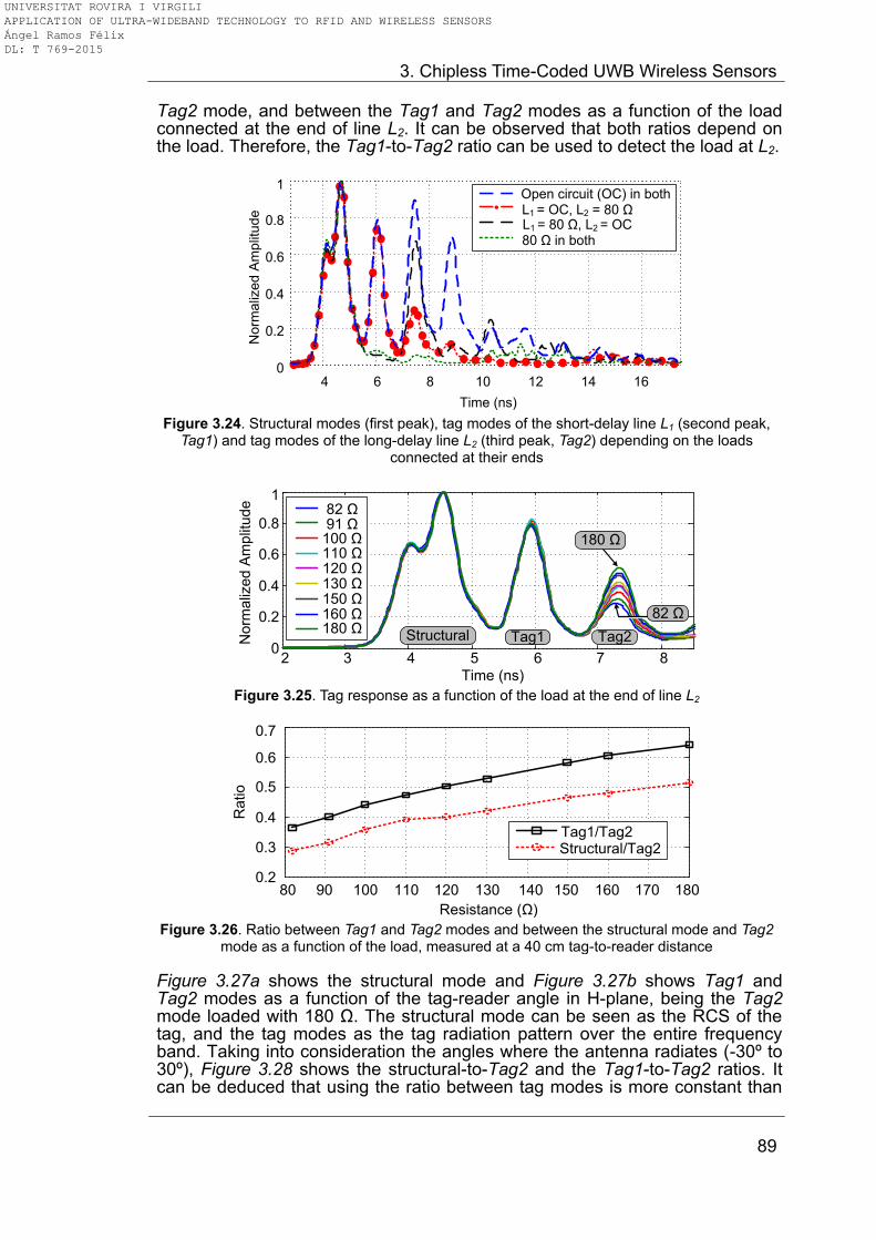
3. Chipless Time-Coded UWB Wireless Sensors
89
Tag2 mode, and between the Tag1 and Tag2 modes as a function of the load connected at the end of line L2. It can be observed that both ratios depend on the load. Therefore, the Tag1-to-Tag2 ratio can be used to detect the load at L2.
4 6 8 10 12 14 160
0.2
0.4
0.6
0.8
1
Time (ns)
Norm
aliz
ed
Am
plit
ud
e
Open circuit (OC) in bothL1 = OC, L2 = 80 ΩL1 = 80 Ω, L2 = OC80 Ω in both
Figure 3.24. Structural modes (first peak), tag modes of the short-delay line L1 (second peak,
Tag1) and tag modes of the long-delay line L2 (third peak, Tag2) depending on the loads connected at their ends
2 3 4 5 6 7 80
0.2
0.4
0.6
0.8
1
Time (ns)
No
rmaliz
ed A
mplit
ude
82 Ω 91 Ω
100 Ω 110 Ω 120 Ω 130 Ω 150 Ω 160 Ω 180 Ω
Structural Tag1 Tag2
180 Ω
82 Ω
Figure 3.25. Tag response as a function of the load at the end of line L2
80 90 100 110 120 130 140 150 160 170 180
Resistance (Ω)
0.2
0.3
0.4
0.5
0.6
0.7
Ra
tio
Tag1/Tag2Structural/Tag2
Figure 3.26. Ratio between Tag1 and Tag2 modes and between the structural mode and Tag2
mode as a function of the load, measured at a 40 cm tag-to-reader distance
Figure 3.27a shows the structural mode and Figure 3.27b shows Tag1 and Tag2 modes as a function of the tag-reader angle in H-plane, being the Tag2 mode loaded with 180 Ω. The structural mode can be seen as the RCS of the tag, and the tag modes as the tag radiation pattern over the entire frequency band. Taking into consideration the angles where the antenna radiates (-30º to 30º), Figure 3.28 shows the structural-to-Tag2 and the Tag1-to-Tag2 ratios. It can be deduced that using the ratio between tag modes is more constant than
UNIVERSITAT ROVIRA I VIRGILI APPLICATION OF ULTRA-WIDEBAND TECHNOLOGY TO RFID AND WIRELESS SENSORS Ángel Ramos Félix DL: T 769-2015
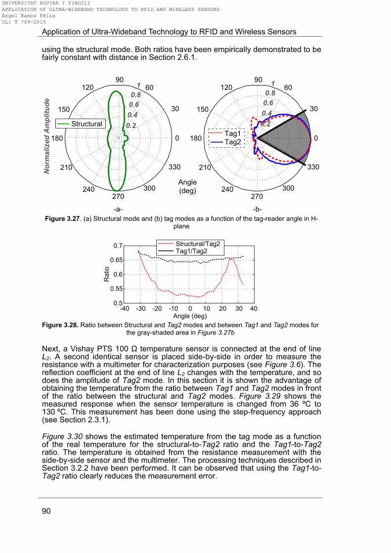
Application of Ultra-Wideband Technology to RFID and Wireless Sensors
90
using the structural mode. Both ratios have been empirically demonstrated to be fairly constant with distance in Section 2.6.1.
30
210
60
240
90
270
120
300
150
330
180 0
Angle
(deg)
0.2
0.4
0.6
0.8
1
Tag1
Tag2
30
210
60
240
90
270
120
300
150
330
180 0
No
rma
lized
Am
plitu
de
0.2
0.4
0.6
0.8
1
Structural
-a- -b-
Figure 3.27. (a) Structural mode and (b) tag modes as a function of the tag-reader angle in H-plane
-40 -30 -20 -10 0 10 20 30 400.5
0.55
0.6
0.65
0.7
Angle (deg)
Ra
tio
Structural/Tag2Tag1/Tag2
Figure 3.28. Ratio between Structural and Tag2 modes and between Tag1 and Tag2 modes for
the gray-shaded area in Figure 3.27b
Next, a Vishay PTS 100 Ω temperature sensor is connected at the end of line L2. A second identical sensor is placed side-by-side in order to measure the resistance with a multimeter for characterization purposes (see Figure 3.6). The reflection coefficient at the end of line L2 changes with the temperature, and so does the amplitude of Tag2 mode. In this section it is shown the advantage of obtaining the temperature from the ratio between Tag1 and Tag2 modes in front of the ratio between the structural and Tag2 modes. Figure 3.29 shows the measured response when the sensor temperature is changed from 36 ºC to 130 ºC. This measurement has been done using the step-frequency approach (see Section 2.3.1). Figure 3.30 shows the estimated temperature from the tag mode as a function of the real temperature for the structural-to-Tag2 ratio and the Tag1-to-Tag2 ratio. The temperature is obtained from the resistance measurement with the side-by-side sensor and the multimeter. The processing techniques described in Section 3.2.2 have been performed. It can be observed that using the Tag1-to-Tag2 ratio clearly reduces the measurement error.
UNIVERSITAT ROVIRA I VIRGILI APPLICATION OF ULTRA-WIDEBAND TECHNOLOGY TO RFID AND WIRELESS SENSORS Ángel Ramos Félix DL: T 769-2015

3. Chipless Time-Coded UWB Wireless Sensors
91
0 5 10 150
0.2
0.4
0.6
0.8
1
Time (ns)
Norm
aliz
ed
Am
plit
ud
e Structural
Tag1
Tag2
7.35 7.4 7.45 7.5 7.55 7.60.38
0.39
0.4
0.41
0.42
Time (ns)
Norm
aliz
ed
Am
plit
ud
e
150 Ω, 130 ºC
114 Ω, 36 ºC
-a- -b- Figure 3.29. (a) Measured tag response as a function of the temperature with the step-
frequency technique at 40 cm and (b) zoomed response of the Tag2 mode
20 40 60 80 100 120 140
Temperature (ºC)
20
40
60
80
100
120
140
160
Estim
ate
d T
em
pe
ratu
re (
ºC)
With Tag1/Tag2 RatioWith Struct./Tag2 Ratio
Figure 3.30. Estimated temperature as a function of the temperature using the ratio between Tag1 and Tag2 modes (solid black line) and using the ratio between the structural and Tag2
modes (dashed red line) measured with the step-frequency technique at 40 cm
Finally, Figure 3.31 shows the same measurement done with the Time Domain radar (Section 2.3.2). An identical behaviour is observed, although the measurement error is larger due to the higher noise of its receiver in front of using a VNA.
20 40 60 80 100 120 140
Temperature (ºC)
20
40
60
80
100
120
140
160
Estim
ate
d T
em
pe
ratu
re (
ºC)
With Tag1/Tag2 RatioWith Struct./Tag2 Ratio
Figure 3.31. Estimated temperature as a function of the temperature using the ratio between Tag1 and Tag2 modes (solid black line) and using the ratio between the structural and Tag2
modes (dashed red line) measured with the impulse technique at 40 cm
UNIVERSITAT ROVIRA I VIRGILI APPLICATION OF ULTRA-WIDEBAND TECHNOLOGY TO RFID AND WIRELESS SENSORS Ángel Ramos Félix DL: T 769-2015
Application of Ultra-Wideband Technology to RFID and Wireless Sensors
92
3.3. Delay-based time-coded chipless sensors Similarly as in Section 3.2, it is possible to sense a physical parameter which changes, in this case, the delay of the tag mode. If a material with a specific permittivity is added on top of the transmission line of a time-coded chipless UWB tag, the permittivity of the medium changes, and therefore the tag mode delay also changes. The main idea is to create a wireless permittivity sensor based on this principle. In this context, a wireless permittivity sensor using chipless frequency-coded UWB RFID is presented in [3.22], detecting dielectric permittivities between 1 and 4.3 at 70 cm of distance. There are several application fields where it is interesting to measure permittivity wirelessly. Capacitive sensors are used for monitoring several maginitudes such as humidity and barometric pressure (this last magnitude depends on the air permittivity). These sensors are based on the variation of the capacitance due to change in the permittivity, as a function of the physical or chemical magnitude. Moreover, variations in the complex dielectric constant can be useful to detect soil composition or variations in civil materials composition, such as the mixture of construction mortars. Aging and long-term evolution of the structure is a major topic in concrete-based buildings [3.23]. Construction aggregate (sand, gravel and rocks) and cement have different permittivities, depending on the percentage of each element. This will be studied in detail in Section 3.3.2.2. 3.3.1. Principle of operation Figure 3.32 shows a scheme of the chipless UWB time-coded permittivity sensor and the signals between the reader and the tag. The permittivity of the medium (transmission line + material added on top) is denoted as εefr. The structural-to-tag mode delay depends on the permittivity of the material. Moreover, the tag mode amplitude depends on the loss of the medium, which, in turn, depends on the loss tangent of the material tanδ2 (the permittivity of the substrate is known). The permittivity of the medium εefr can be calculated using the conformal mapping method proposed in [3.24]. In this case, a two-layer structure is considered, where εr1 is the tag substrate permittivity, εr2 is the material permittivity, w is the transmission line width, h is the substrate thickness and h2-h
is the material thickness. εefr can be expressed as:
2
1
1 1 2
2 1 2 2
1
1efr r r
r
q q q
. (3.7)
If w/h > 1, then the filling factors q1 and q2 are:
UNIVERSITAT ROVIRA I VIRGILI APPLICATION OF ULTRA-WIDEBAND TECHNOLOGY TO RFID AND WIRELESS SENSORS Ángel Ramos Félix DL: T 769-2015

3. Chipless Time-Coded UWB Wireless Sensors
93
1
ln 11
12
ef
ef
wh
qw h
,
(3.8)
2 1
2
cos1 2
1 ln sin12 2
2 2
e
efe e
eef
v
wh v vhq q
vhw h h
h h
, (3.9)
where wef and ve are:
2ln 17.08 0.92
2ef
h ww w
h
(3.10)
22 1
22
eef
hhv arctg
w hh
. (3.11)
If w/h < 1, the filling factors q1 and q2 are:
1
1 1 81 arccos
2 4 2 8
w hq
h w
(3.12)
2
2
0.9 ln arccos 1 14 81
2 ln 8
h wb bh h
qh w
, (3.13)
where b is defined as:
2
2
1
4 1
h hb
h h w h
. (3.14)
Figure 3.33 shows the calculated medium permittivity for the w/h < 1 and the w/h > 1 cases. An εr1 = 3.55 and h = 0.813 mm have been chosen, which correspond to a Rogers RO4003C substrate (see Table 2.3). As it can be observed, for both cases the permittivity remains practically constant for material heights greater than 4 mm. Therefore, in practice the medium permittivity will depend only on εr2. It can also be observed that εefr is more sensitive for the w/h < 1 case. Therefore, the tag should be designed with a ratio w/h < 1.
UNIVERSITAT ROVIRA I VIRGILI APPLICATION OF ULTRA-WIDEBAND TECHNOLOGY TO RFID AND WIRELESS SENSORS Ángel Ramos Félix DL: T 769-2015
Application of Ultra-Wideband Technology to RFID and Wireless Sensors
94
Tr. Line (εr1)
L
Material (εr2, tanδ2)
Med
ium
(εefr )
UWB
Antenna
Time
Struct.
Mode
Time
p(t)Transmitted
Backscattered
S21
S12 S2
2
S1
1
Tag
ModeCoupl.
Reader
Tx
Tagf (εefr)
f (tanδ2,
εefr)
Reader
Rx
Figure 3.32. Scheme of the wireless chipless permittivity sensor and signals between the tag
and the reader
0 2 4 6 8 102.5
3
3.5
4
h2 - h (mm)
efr
w/h < 1
1
2
3
4
5
-a-
0 1 2 3 4 52.85
2.9
2.95
h2 - h (mm)
efr
1 2 3 4 5
r2
w/h > 1
-b-
-c-
Figure 3.33. Calculated εefr for the (a) w/h < 1 case and (b) w/h > 1 case. (c) Detail of the case where w/h < 1 with a continuous sweep. The material height h is swept from 1 to 10 and its
permittivity εr2 from 1 to 5
For the case of interest (w/h < 1), the characteristic impedance Z0 of the multilayer transmission line can be expressed as:
0
60 8ln
efr
hZ
w
, (3.15)
1
2
3
4
5 02
46
810
2
3
4
h2 - h (mm)
r2
efr
UNIVERSITAT ROVIRA I VIRGILI APPLICATION OF ULTRA-WIDEBAND TECHNOLOGY TO RFID AND WIRELESS SENSORS Ángel Ramos Félix DL: T 769-2015

3. Chipless Time-Coded UWB Wireless Sensors
95
and it is plotted in Figure 3.34, for a w = 0.7 mm. It can be observed how the change in the material permittivity mismatches the impedance between the antenna (designed to be an impedance of 83 Ω) and the transmission line attached to the material. Therefore, the tag mode amplitude will depend both on the loss tangent and the permittivity of the material and no change is observed for material heights greater than 4 mm.
0 2 4 6 8 1065
70
75
80
85
h2 - h (mm)
Z 0 (
)
1 2 3 4 5
r2
Matched case
Mismatching between
antenna and line
Figure 3.34. Impedance of the medium (transmission line) as a function of the permittivity and
height of the material added on top of it
3.3.2. Permittivity sensor based on chipless time-coded UWB tags Two tag approaches are designed and simulated for chipless UWB time-coded permittivity sensors, both on Rogers RO4003C substrate (see Table 2.3). Then, the tag with the best performance is used in a real application to detect concrete composition. 3.3.2.1. Sensor design The first permittivity sensor tag consists of the small monopole from Section 2.6.2, but the delay line length L has been increased to increase time resolution. By increasing L there will be a greater change in ΔηL due to the attached material. Five thick slabs of materials are considered, with a thickness of 1 cm, which is much larger than the 4 mm required (see Section 3.3.1). The materials characterized and their respective permittivities are: PTFE (2.2), PC (3.2), PET (3.6), PUR (4) and CARP (5.7). Figure 3.35a shows the layout of the designed tag. The tag size is 34.5 mm x 69 mm. Figure 3.35b shows the simulated |S11| parameter. Finally, Figure 3.35c shows the designed tag with one material attached on top of the transmission line in the simulation environment.
The response of the tag when on contact with the materials is simulated using Ansys HFSS, with a plane wave orientated towards the tag bottom face, and a vacuum box to set a distance of 40 cm. The plane wave is oriented at the back face for simplicity. Otherwise, the contribution of the material would appear before the contribution of the structural mode of the tag.
UNIVERSITAT ROVIRA I VIRGILI APPLICATION OF ULTRA-WIDEBAND TECHNOLOGY TO RFID AND WIRELESS SENSORS Ángel Ramos Félix DL: T 769-2015

Application of Ultra-Wideband Technology to RFID and Wireless Sensors
96
Bottom
Top
-a-
1 3 5 7 9-30
-20
-10
0
Frequency (GHz)
|S11
| (d
B)
-b-
-c-
Figure 3.35. (a) Layout of the tag. (b) Simulated |S11|. (c) Scheme of the simulated tag with attached material
Figure 3.36 shows the time-domain response of the tag before and after applying the CWT technique from Section 2.4.2. As it can be observed, the structural mode remains invariant for all the measurements, while the tag mode delay increases when the permittivity of the material increases.
1 1.5 2 2.5 3 3.5 4-1
-0.5
0
0.5
1
Time (ns)
No
rma
lize
d A
mp
litu
de
0
0.2
0.4
0.6
0.8
1
No
rma
lize
d A
mp
litu
de
1 1.5 2 2.5 3 3.5 4Time (ns)
Structural
Modes
Tag
Modes
Air (1)PTFE (2.2)PC (3.2)PET (3.6)PUR (4)CARP (5.7)
-a- -b- Figure 3.36. Simulated time-domain response of the tag with several materials attached on top of the transmission line. (a) RAW signal. (b) Continuous Wavelet Transform has been applied to
the RAW signal
Figure 3.37a shows the structural to tag mode delay as a function of the permittivity of the material attached to the transmission line. A linear behaviour can be observed. Figure 3.37b shows the delay increase with respect to air (εr2 = 1) case. Again, a linear behaviour is observed, with a delay increase from 100 ps to 350 ps. Finally, Figure 3.38 shows the structural to tag mode ratio as a function of the permittivity of the material. The material reduces the tag mode amplitude. It will be studied in detail next.
UNIVERSITAT ROVIRA I VIRGILI APPLICATION OF ULTRA-WIDEBAND TECHNOLOGY TO RFID AND WIRELESS SENSORS Ángel Ramos Félix DL: T 769-2015
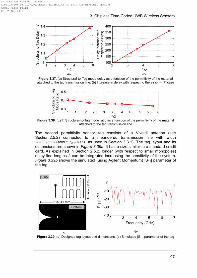
3. Chipless Time-Coded UWB Wireless Sensors
97
2 3 4 5 6 r2
De
lay in
cre
ase
with
respe
ct
to A
ir (
ps)
1 2 3 4 5 61
1.1
1.2
1.3
1.4
r2
Str
uctu
ral to
Ta
g D
ela
y (
ns)
100
150
200
250
300
350
400
-a- -b- Figure 3.37. (a) Structural-to-Tag mode delay as a function of the permittivity of the material
attached to the tag transmission line. (b) Increase in delay with respect to the air (εr2 = 1) case
1 1.5 2 2.5 3 3.5 4 4.5 5 5.5 6
Str
uctu
ral to
Tag
Mode R
atio
0.3
0.4
0.5
r2 Figure 3.38. (Left) Structural-to-Tag mode ratio as a function of the permittivity of the material
attached to the tag transmission line
The second permittivity sensor tag consists of a Vivaldi antenna (see Section 2.5.2) connected to a meandered transmission line with width w = 0.7 mm (about Z0 = 83 Ω, as used in Section 3.3.1). The tag layout and its dimensions are shown in Figure 3.39a. It has a size similar to a standard credit card. As explained in Section 2.5.2, longer (with respect to small monopoles) delay line lengths L can be integrated increasing the sensitivity of the system. Figure 3.39b shows the simulated (using Agilent Momentum) |S11| parameter of the tag.
Top
102.41 mm
57
.87
mm
Bottom
-a-
2 3 4 5 6 7
Frequency (GHz)
-40
-30
-20
-10
0
|S11
| (d
B)
-b-
Figure 3.39. (a) Designed tag layout and dimensions. (b) Simulated |S11| parameter of the tag
UNIVERSITAT ROVIRA I VIRGILI APPLICATION OF ULTRA-WIDEBAND TECHNOLOGY TO RFID AND WIRELESS SENSORS Ángel Ramos Félix DL: T 769-2015
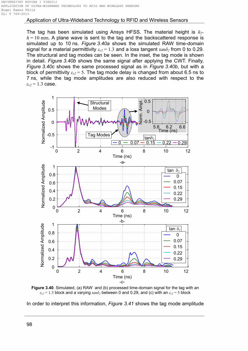
Application of Ultra-Wideband Technology to RFID and Wireless Sensors
98
The tag has been simulated using Ansys HFSS. The material height is h2-
h = 10 mm. A plane wave is sent to the tag and the backscattered response is simulated up to 10 ns. Figure 3.40a shows the simulated RAW time-domain signal for a material permittivity εr2 = 1.3 and a loss tangent tanδ2 from 0 to 0.29. The structural and tag modes can be seen. In the inset, the tag mode is shown in detail. Figure 3.40b shows the same signal after applying the CWT. Finally, Figure 3.40c shows the same processed signal as in Figure 3.40b, but with a block of permittivity εr2 = 5. The tag mode delay is changed from about 6.5 ns to 7 ns, while the tag mode amplitudes are also reduced with respect to the εr2 = 1.3 case.
0 2 4 6 8 10 12-1
-0.5
0
0.5
1
Time (ns)
No
rma
lize
d A
mp
litu
de
Tag Modes
Structural
Modes
0 0.07 0.15 0.22 0.29tan2
5.8 6.2 6.6
-0.5
0
0.5
Time (ns)
No
rm. A
mp
l.
0 2 4 6 8 10 120
0.2
0.4
0.6
0.8
1
Time (ns)
No
rma
lize
d A
mp
litu
de
0
0.07
0.15
0.22
0.29
tan 2
0 2 4 6 8 10 120
0.2
0.4
0.6
0.8
1
Time (ns)
No
rma
lize
d A
mp
litu
de
0
0.07
0.15
0.22
0.29
tan 2
-a-
-b-
-c- Figure 3.40. Simulated, (a) RAW and (b) processed time-domain signal for the tag with an
εr2 = 1.3 block and a varying tanδ2 between 0 and 0.29, and (c) with an εr2 = 5 block
In order to interpret this information, Figure 3.41 shows the tag mode amplitude
UNIVERSITAT ROVIRA I VIRGILI APPLICATION OF ULTRA-WIDEBAND TECHNOLOGY TO RFID AND WIRELESS SENSORS Ángel Ramos Félix DL: T 769-2015
3. Chipless Time-Coded UWB Wireless Sensors
99
as a function of both the material permittivity and the loss tangent. It can be observed that, for εr2 > 3, the tag mode amplitude change mainly depends on the loss tangent of the material.
0 0.05 0.1 0.15 0.2 0.25 0.3 0.35tan
Ta
g M
od
e
Am
plit
ud
e
2
1.3 2 3 4 5r2
0
0.2
0.4
0.6
Figure 3.41. Simulated tag mode amplitude as a function of the material permittivity and loss
tangent
Next, the tag is simulated attaching a 10 mm-thick material with no loss and varying the permittivity, similarly as with the small monopole case. The tag mode delay changes according to the permittivity, while the tag mode amplitude depends on the mismatching between the UWB antenna and the medium with the material. Figure 3.42 shows the simulated, processed time-domain response. The signal is normalized with respect to the absolute maximum, which is the structural mode for εr2 = 1. In this case, the structural mode amplitude varies depending on the permittivity. This is because the Vivaldi antenna has a smaller RCS than a UWB monopole. The absorption due to the material affects the structural mode amplitude. Figure 3.43 shows the amplitude of the tag mode as a function of εr2. The same behaviour as in Figure 3.41 is observed. For permittivities εr2 > 3, the tag mode amplitude does not vary. Finally, the tag mode delay is shown in Figure 3.44 as a function of εr2. As with the small monopole case (see Figure 3.37), a linear behaviour is observed.
0 2 4 6 8 10 120
0.2
0.4
0.6
0.8
1
Time (ns)
No
rma
lize
d
Am
plit
ud
e
r2 = 1r2 = 2r2 = 3r2 = 4r2 = 5
Figure 3.42. Simulated, processed time-domain signal for the tag with a non-lossy material with
permittivities from 1 to 5
1 1.5 2 2.5 3 3.5 4 4.5 50.35
0.4
0.45
0.5
r2
Tag
Mode
Am
plit
ude
Figure 3.43. Tag mode amplitude as a function of εr2, with tanδ2 = 0 (lossless material)
UNIVERSITAT ROVIRA I VIRGILI APPLICATION OF ULTRA-WIDEBAND TECHNOLOGY TO RFID AND WIRELESS SENSORS Ángel Ramos Félix DL: T 769-2015
Application of Ultra-Wideband Technology to RFID and Wireless Sensors
100
1 1.5 2 2.5 3 3.5 4 4.5 55.5
6
6.5
7
7.5
Tag M
ode
De
lay (
ns)
r2 Figure 3.44. Tag mode delay as a function of εr2
3.3.2.2. Concrete composition detection Structural health of concrete-based civil structures is a major concern in today’s society. Detecting the quality of the materials used in civil engineering is necessary to ensure safe structures, such as buildings or bridges [3.25]. Unexpected events such as earthquakes, hurricanes, or simply a material deterioration because of a wrong mixture of compounds, could cause a structure to collapse. During the construction period, samples of the construction compounds are usually inspected. However, long-term non-destructive testing (NDT) of the civil structure is also desired. In this context, several works have been presented recently, with the aim of wirelessly sense these structures. Battery-powered active sensors, using microcontrollers and accelerometers are reviewed in [3.25]. One of the main materials used in this type of structures is concrete. Specifically, a mixture of concrete and dry sand. The permittivity of these two materials has been studied at the microwave frequency range. A passive permittivity sensor which uses UHF RFID at 870 MHz is presented in [3.26]. A UHF RFID sensor is presented to detect the permittivity of lightweight concrete in [3.27]. The dielectric constant of concrete is obtained in [3.28] by measuring the deflection and loss of electromagnetic waves in concrete blocks using a CW radar. In [3.29] the permittivity of concrete is measured between 0 and 20 GHz using a probe and a Network Analyzer. In [3.30] the permittivity of dry sand is measured up to 6 GHz using microwave resonators. A wireless water content sensor based on a 22.5 MHz inductive-capacitive circuit is presented in [3.31]. Next, the Vivaldi-based permittivity sensor tag will be used as a battery-less concrete composition (concrete and sand) sensor. In addition, a method to calibrate the tag is presented to obtain the concrete composition.
Figure 3.45a shows a scheme of the system. The delay line is embedded in concrete, as shown in both the scheme the tag (Figure 3.45b) layers (Figure 3.45c) and photographs (Figure 3.45d). The signal at the reader’s receiving (Rx) antenna in time domain can be approximated as the sum of several peaks (see Section 2.2):
. .( ) ( ) ( ) ( ) ( ) ( ) ( )Coupl Clutter Str Plate Concrete Tags t s t s t s t s t s t s t , (3.16)
where sCoupl. is the coupling from the reader Tx to Rx antenna and sClutter is the
UNIVERSITAT ROVIRA I VIRGILI APPLICATION OF ULTRA-WIDEBAND TECHNOLOGY TO RFID AND WIRELESS SENSORS Ángel Ramos Félix DL: T 769-2015
3. Chipless Time-Coded UWB Wireless Sensors
101
clutter from the scene. Both can be removed by windowing and background
subtraction (see Section 2.4.1). sStr. corresponds to the tag structural mode,
which depends on the tag shape, size and material. A Vivaldi antenna has a
small radar cross-section (RCS) in its optimum radiation pattern H-plane angle.
Therefore, its structural mode is small and difficult to detect. A metal plate is
soldered in the Vivaldi ground plane in perpendicular to the Vivaldi ground
plane, providing a strong reference peak. This plate is separated from the
tapered transition so it does not affect the antenna. sPlate corresponds to the
signal backscattered at the metal plate, sConcrete corresponds to the reflection at
the concrete slab or wall. Finally, sTag corresponds to the tag mode, which
depends on the load of the antenna (here an open-ended delay line). sTag is the
part of p(t) that propagates inside the tag and is reradiated to the reader with
the information of the material where the line is embedded.
The Vivaldi antenna has been chosen because it permits to integrate a long meander delay without having undesired effects, as studied in Section 2.5.2. Also, its gain has shown to be larger than the other studied alternatives, and its boresight is perpendicular to the concrete wall or slab. As shown in Figure 3.45a, the signals corresponding to sStr. and sConcrete are unstable in time, because of changes in angle or distance from one measurement to another, and because of dispersion, respectively. Therefore, sPlate is used as reference, which also denotes the limit where the tag should be embedded in concrete. The delay between sPlate and sTag is addressed as η. η depends on the delay line length L and the propagation speed of the medium v, which, in turn, depends on the effective permittivity of the medium εefr. εefr, in turn, depends on the permittivities of both the substrate (εr1) and the concrete slab (εr2). Finally, the term 2d/c (c = 3 · 108 m/s) accounts for the distance d between the tag and the reader, from which η is independent of.
3.3.2.3. Results In order to obtain the concrete layer permittivity, a relationship between the effective permittivity of the multilayer microstrip and the concrete layer permittivity is needed. The S parameters of a multilayer microstrip transmission line of width w = 0.7 mm on RO4003C (see Table 2.3) have been simulated with Agilent Momentum. The structure follows the scheme of Figure 3.45c, the concrete layer height is h2 - h = 10 mm and εr2 is swept from 1 to 5. A line of length L = 2.5 mm is chosen to minimize the time required for the simulation. The effective permittivity εefr of the multilayer structure is obtained from the expression of S parameters of a transmission line. Then:
11
21
acoshl
Z
Z
, (3.17)
Im l
L
, (3.18)
UNIVERSITAT ROVIRA I VIRGILI APPLICATION OF ULTRA-WIDEBAND TECHNOLOGY TO RFID AND WIRELESS SENSORS Ángel Ramos Félix DL: T 769-2015

Application of Ultra-Wideband Technology to RFID and Wireless Sensors
102
2
2efr
c
f
, (3.19)
where Z11 and Z21 are the simulated Z parameters of the multilayer transmission
line, and f is the frequency. Since the reader is based on the Time Domain
radar (see Section 2.3.2), which is centered at 4.3 GHz, the permittivity εefr at
this frequency is chosen for each simulated εr2 case. Figure 3.46 shows the
resulting curve. A nearly-linear behaviour is obtained, as the one observed in
Figure 3.33c for thicknesses greater than 4 mm.
UWB
Antenna
L
Time
Str
uct. M
od
e
τ
Time
p(t)
S21
S12
S22S11
Tag M
od
e
Co
uplin
g
Tx Ant.
Rx Ant.
Sensor Tag
(Zc , εr1)
Reader
Metal
plate
Concrete embedded
Meta
l p
late
Co
ncre
te laye
r
2d/c
-a-
Top
Bottom
Metal PlateAntenna
(on Air)Embedded
Delay Line (εr1)
Metal
Plate Concrete
(εr2)
-b-
w
εr1
εr2
ε0
h2h
Concrete
RO4003C
Air
-c-
Metal Plate
-d- Figure 3.45. (a) Scheme of the tag-reader system. (b) Scheme of the tag embedded in
concrete. (c) Scheme of the layers in the tag. (d) Photograph of the tag embedded in concrete (left) and cut of the concrete layer (right)
UNIVERSITAT ROVIRA I VIRGILI APPLICATION OF ULTRA-WIDEBAND TECHNOLOGY TO RFID AND WIRELESS SENSORS Ángel Ramos Félix DL: T 769-2015

3. Chipless Time-Coded UWB Wireless Sensors
103
1 1.5 2 2.5 3 3.5 4 4.5 5
3
4
r2
efr
Figure 3.46. Simulated effective permittivity of the multilayer structure
The proposed tag with the concrete block (see Figure 3.45b) has been simulated using Ansys HFSS. A 10 mm thick concrete block is added on top of the tag delay line. The permittivity of this block (εr2) is again swept from 1 to 5, with 20 samples within the range. Figure 3.47 shows the simulated time-domain signal before and after applying the CWT. It is important to note that not all the samples of εr2 are shown for representation convenience. On the contrary as the case simulated in Figure 3.42, in this case the metal plate fixes the time reference, while the tag mode varies depending on εr2.
-1
-0.5
0
0.5
1
No
rma
lize
d A
mp
litu
de
1.001.421.842.262.683.113.533.954.374.79
Permittivity (εr2)
Metal
PlateStructural Modes
Tag Modes
0 1 2 3 4 5 6 7 8 9 100
0.2
0.4
0.6
0.8
1
Time (ns)
1.6 1.8 20
0.5
1
Time (ns)No
rm. A
mp
l.
Tag
Modes
Metal Plate
Figure 3.47. Simulated time-domain signal of the tag for εr2 from 1 to 5. (top) RAW signal.
(bottom) Signal after applying the CWT
Three concrete blocks (A, B and C) are fabricated with an embedded tag. The blocks are composed of a mixture of portland concrete and sand. The compositions are depicted in Table 3.2. The blocks have been dried in still air for four weeks before measuring them. Three sets of 100 measurements have been performed at a 40 cm tag-reader distance. Figure 3.48 shows the measured time-domain response of the blocks after applying the CWT. The background subtraction technique (see Section 2.4.1) is also applied. In the case of concrete walls, the background can be obtained from a tag-free portion of the wall at the same distance. The mean delays between the metal plate
and the tag modes are shown in Table 3.2. The tag mode amplitude is reduced when the tag is embedded in concrete but the peaks and the time difference can still be perfectly detected. The measured delay η can be modeled as:
UNIVERSITAT ROVIRA I VIRGILI APPLICATION OF ULTRA-WIDEBAND TECHNOLOGY TO RFID AND WIRELESS SENSORS Ángel Ramos Félix DL: T 769-2015
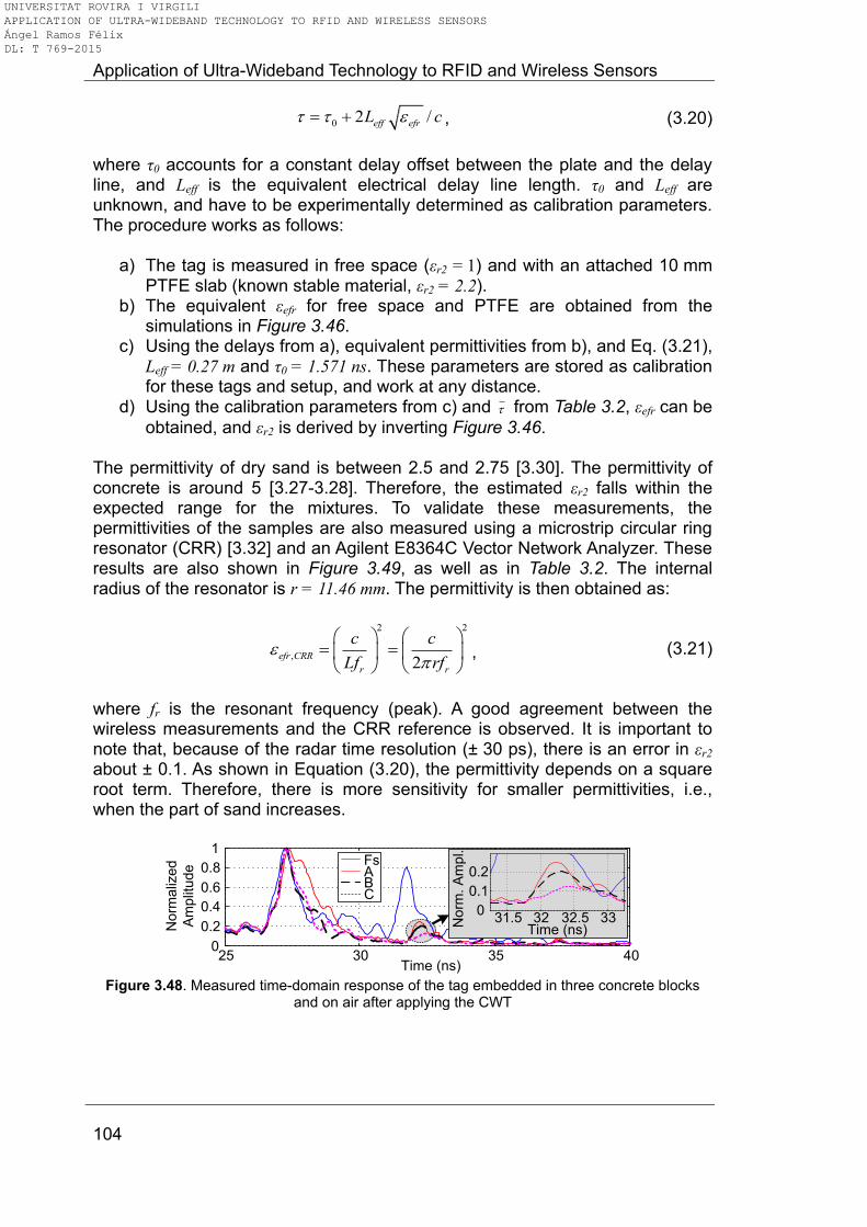
Application of Ultra-Wideband Technology to RFID and Wireless Sensors
104
0 2 /eff efrL c , (3.20)
where η0 accounts for a constant delay offset between the plate and the delay line, and Leff is the equivalent electrical delay line length. η0 and Leff are unknown, and have to be experimentally determined as calibration parameters. The procedure works as follows:
a) The tag is measured in free space (εr2 = 1) and with an attached 10 mm PTFE slab (known stable material, εr2 = 2.2).
b) The equivalent εefr for free space and PTFE are obtained from the simulations in Figure 3.46.
c) Using the delays from a), equivalent permittivities from b), and Eq. (3.21), Leff = 0.27 m and η0 = 1.571 ns. These parameters are stored as calibration for these tags and setup, and work at any distance.
d) Using the calibration parameters from c) and from Table 3.2, εefr can be
obtained, and εr2 is derived by inverting Figure 3.46.
The permittivity of dry sand is between 2.5 and 2.75 [3.30]. The permittivity of concrete is around 5 [3.27-3.28]. Therefore, the estimated εr2 falls within the expected range for the mixtures. To validate these measurements, the permittivities of the samples are also measured using a microstrip circular ring resonator (CRR) [3.32] and an Agilent E8364C Vector Network Analyzer. These results are also shown in Figure 3.49, as well as in Table 3.2. The internal radius of the resonator is r = 11.46 mm. The permittivity is then obtained as:
2 2
,2
efr CRR
r r
c c
Lf rf
, (3.21)
where fr is the resonant frequency (peak). A good agreement between the wireless measurements and the CRR reference is observed. It is important to note that, because of the radar time resolution (± 30 ps), there is an error in εr2 about ± 0.1. As shown in Equation (3.20), the permittivity depends on a square root term. Therefore, there is more sensitivity for smaller permittivities, i.e., when the part of sand increases.
25 30 35 400
0.2
0.4
0.6
0.8
1
Time (ns)
Norm
aliz
ed
Am
plit
ude
31.5 32 32.5 330
0.1
0.2
Time (ns)
Norm
. A
mpl.
FsABC
Figure 3.48. Measured time-domain response of the tag embedded in three concrete blocks
and on air after applying the CWT
UNIVERSITAT ROVIRA I VIRGILI APPLICATION OF ULTRA-WIDEBAND TECHNOLOGY TO RFID AND WIRELESS SENSORS Ángel Ramos Félix DL: T 769-2015
3. Chipless Time-Coded UWB Wireless Sensors
105
Block Number % C % S Delay
(ns) ± ζ Estimated εr2 Ref. εr2 CRR
A 25 75 5.000 3.56 3.51
B 50 50 5.070 3.98 4.07
C 100 0 5.125 4.31 4.24
% C: Percentage of Concrete, % S: Percentage of Sand, ζ = 30 ps
Table 3.2. Concrete blocks composition
1.6 1.8 2 2.2 2.4 2.6 2.8 3-60
-50
-40
-30
-20
Frequency (GHz)
|S21
| (d
B)
Free SpaceABC
r
r = 11.46 mm
Figure 3.49. (Left) Simulated |S21| parameter of a microstrip circular ring resonator with the
samples on top. (Right) Photograph of the circular ring resonator
3.4. Conclusions This chapter has presented the realization of several chipless UWB time-coded sensors. Two main approaches have been studied: amplitude-based sensors and delay-based sensors. The following conclusions have been obtained:
It is possible to realize chipless temperature sensors by using a simple Platinum resistor at the end of a chipless time-coded UWB tag to detect temperature in the 30-130 ºC range
The designed sensor provides the temperature from the tag mode amplitude of the backscattered signals and the tag is identified by the delay of the line connected to the antenna
Reliable measurements up to a distance of 1 meter have been obtained, which is a smaller distance than the 2 m for just identification (see Section 2.6.1)
A characterization of the system as a function of the angle between the reader and the tag sensor has also been done. A good performance for all angles, except for the radiation nulls of the UWB antenna, is demonstrated
Calibration is a major concern to obtain a reliable measurement. With a chipless tag which generates two simultaneous states, it can be achieved. It permits to independize the sensor from the illumination angle
UNIVERSITAT ROVIRA I VIRGILI APPLICATION OF ULTRA-WIDEBAND TECHNOLOGY TO RFID AND WIRELESS SENSORS Ángel Ramos Félix DL: T 769-2015
Application of Ultra-Wideband Technology to RFID and Wireless Sensors
106
within the beamwidth of the tag antenna
If it is only needed to measure whether a threshold has been surpassed, more advanced processing techniques can be applied, increasing the reading distance from 1-2 meters up to 5 meters
Concrete composition detection can also be remotely measured using very inexpensive chipless tags. This is desirable in civil engineering for classification purposes and long-term quality evaluation, where the number of sensors is expected to be very large
3.5. Bibliography [3.1] S. Shrestha, M. Balachandran, M. Agarwal, V. V. Phoha, and K. Varahramyan, “A
Chipless RFID Sensor System for Cyber Centric Monitoring Applications,” IEEE Transactions on Microwave Theory and Techniques, Vol. 57, No. 5, pp. 1303-1309, May 2009.
[3.2] T. T. Thai, J. M. Mehdi, H. Aubert, P. Pons. G. DeJean, M. M. Tentzeris, and R. Plana, “A
novel passive wireless ultrasensitive RF temperature transducer for remote sensing,” IEEE MTT-S Microwave Symposium Digest, pp. 473-476, 2010.
[3.3] M. M. Jatlaoui, F. Chebila, I. Gmati, P. Pons, and H. Aubert, “New electromagnetic
transduction micro-sensor concept for passive wireless pressure monitoring application,” 15th Intl. Conference on Solid-State Sensors, Actuators and Microsystems, Jun. 2009, Colorado, USA.
[3.4] M. A. Fonseca, J. M. English, M. V. Arx, and M. G. Allen, “Wireless micromachined
ceramic pressure sensor for high-temperature applications,” IEEE Journal of Microelectromechanical Systems, Vol. 11, No. 4, pp. 337-343, Aug. 2002.
[3.5] A. Vena, E. Perret, S. Tedjini, D. Kaddour, A. Pottie, and T. Barron, "A Compact
Chipless RFID Tag with Environment Sensing Capability," 2012 IEEE MTT-S International Microwave Symposium Digest (MTT), pp. 1-3, 2012.
[3.6] L. M. Reindl and I. M. Shrena, “Wireless measurement of temperature using surface
acoustic waves sensors,” IEEE Transactions on Ultrasonics, Ferroelectrics and Frequency Control, Vol. 51, No. 11, pp. 1457-1463 Nov. 2004.
[3.7] J. Dowling, M. M. Tentzeris, and N. Becket, “RFID-enabled temperature sensing
devices: A major step forward for energy efficiency in home and industrial applications?,” IEEE MTT-S Intl. Microwave Workshop on Wireless Sensing, Local Positioning, and RFID, pp. 1-4, 2009.
[3.8] K. Along, Z. Chenrui, Z. Luo, L. Xiaozheng, and H. Tao, “SAW RFID enabled multi-
functional sensors for food safety applications,” IEEE Intl. Conference on RFID-Technology and Applications 2010, pp. 200-204, 2010.
[3.9] Vishay Beyschlag “Platinum SMD Flat Chip Temperature Sensor,”
http://www.vishay.com/docs/28762/28762.pdf, Nov. 2014 [Nov. 1, 2014].
[3.10] Agilent Technologies, "De-embedding and Embedding S-Parameter Networks Using a Vector Network Analyzer," Application Note 1364-1, 2004.
UNIVERSITAT ROVIRA I VIRGILI APPLICATION OF ULTRA-WIDEBAND TECHNOLOGY TO RFID AND WIRELESS SENSORS Ángel Ramos Félix DL: T 769-2015
3. Chipless Time-Coded UWB Wireless Sensors
107
[3.11] A. P. Sample, D. J. Yeager, P. S. Powledge, A. V. Mamishev, and J. R. Smith, “Design of an RFID-based battery-free programmable sensing platform,” IEEE Transactions on Instrumentation and Measurement, Vol. 57, No. 11, pp. 2608-2615, Nov. 2008.
[3.12] K. Opasjumruskit, T. Thanthipwan, O. Sathusen, et al., “Self-powered wireless
temperature sensors exploit RFID technology,” IEEE Pervasive Computing, Vol. 5, No. 1, pp. 54-61, Jan. 2006.
[3.13] J. Yin, J. Yi, M. K. Law, et al. “A system-on-chip EPC Gen-2 passive UHF RFID tag with
embedded temperature sensor,” IEEE Journal of Solid-State Circuits, Vol. 45, No. 11, pp. 2404-2420, Nov. 2010.
[3.14] F. Zito, L. Fragomeni, F. Aquilino, and F. G, Della Corte, “Wireless Temperature Sensor
Integrated Circuits with on-chip Antennas,” 15th IEEE Mediterranean Electrotechnical Conference, pp. 1368-1373, 2010.
[3.15] J. Virtanen, L. Ukkonen, T. Björninen, L. Sydänheimo, A. Z. Elsherbeni, “Temperature
Sensor Tag for Passive UHF RFID Systems,” IEEE Sensors and Applications Symposium, pp. 312-317, 2011.
[3.16] W. Che, D. Meng, X. Xang, et al., “A Semi-Passive UHF RFID Tag with On-Chip
Temperature Sensor,” IEEE Custom Integrated Circuits Conference, pp. 1-4, 2010.
[3.17] R. Bhattacharyya, C. Floerkemeier, and S. Sarma, “RFID tag antenna based temperature sensing,” Proc. IEEE International Conference on RFID, pp. 8–15, 2010.
[3.18] J. Gao, J. Siden, and H-K. Nilsson, “Printed Temperature Sensors for Passive RFID
Tags,” Proc. Progress In Electromagnetics Research Symp., Xi’an, China, pp. 845-848, 2010.
[3.19] S. Caizzone, C. Occhiuzzi, and G. Marrocco, “Multi-Chip RFID Antenna Integrating
Shape-Memory Alloys for Detection of Thermal Thresholds,” IEEE Transactions on Antennas and Propagation, Vol. 59, No. 7, pp. 2488-2494, 2011.
[3.20] Y. Fu, H. Du, W. Huang, S. Zhang, and M. Hu, “TiNi-based thin films in MEMS
applications: a review,” Sensors and Actuators A, Vol. 112, pp. 395-408, 2004.
[3.21] W. M. Huang, Z. Ding, C. C. Wang, J. Wei, Y. Zhao, and H. Purnawali, “Shape memory
materials,” Materials Today, Vol. 13, No. 7-8, pp. 54-61, 2010.
[3.22] D. Girbau, A. Lazaro, and R. Villarino, “Passive wireless permittivity sensor based on
frequency-coded chipless RFID tags,” 2012 IEEE MTT-S International Microwave Symposium Digest, pp. 1-3, 2012.
[3.23] Y. Mori and B. R. Ellingwood, “Reliability-based service-life assessment of aging
concrete structures,” Journal of Sctructural Engineering, Vol. 119, No. 5, pp. 1600-1621, 1993.
[3.24] J. Svacina, “A Simple Quasi-Static Determination of Basic Parameters of Multilayer
Microstrip and Coplanar Waveguide,” IEEE Microwave And Guided Wave Letters, Vol. 2, No. 10, pp. 385-387, 1992.
[3.25] J. P. Lynch, “An overview of wireless structural health monitoring for civil structures,”
Phil. Trans. R. Soc. A, Vol. 365, No. 1851, pp. 345-372, 2007.
[3.26] G. Marrocco, L. Mattioni, and C. Calabrese, “Multiport Sensor RFIDs for Wireless Passive Sensing of Objects - Basic Theory and Early Results,” IEEE Transactions on Antennas and Propagation, Vol. 51, No. 1, pp. 31-39, 2003.
UNIVERSITAT ROVIRA I VIRGILI APPLICATION OF ULTRA-WIDEBAND TECHNOLOGY TO RFID AND WIRELESS SENSORS Ángel Ramos Félix DL: T 769-2015
Application of Ultra-Wideband Technology to RFID and Wireless Sensors
108
[3.27] R. Suwalak, C. Phongcharoenpanich, D. Torrungrueng, and M. Krairiksh, “Determination of Dielectric Property of Construction Material Products Using a Novel RFID Sensor,” Progress in Electromagnetics Research, Vol. 130, pp. 601-617, 2014.
[3.28] X. Hui, L. Bangyu, X. Shaobo, and F. Hongzhuan, “The Measurement of Dielectric
Constant of the Concrete Using Single-frequency CW Radar,” First Intl. Conf. On Intelligent Networks and Intelligent Systems, pp. 588-591, 2008.
[3.29] H. C. Rhim and O. Buyukozturk, “Electromagnetic Properties of Concrete at Microwave
Frequency Range,” ACI Materials Journal, Vol. 95, No. 3, pp. 262-271, 1998.
[3.30] C. Matzler, “Microwave Permittivity of Dry Sand,” IEEE Transactions on Geoscience and Remote Sensing, Vol. 36, No. 1, pp. 317-319, Jan. 1998.
[3.31] J. B. Ong, Z. You, J. Mills-Beale, E. L. Tan, B. D. Pereles, and K. G. Ong, "A Wireless,
Passive Embedded Sensor for Real-Time Monitoring of Water Content in Civil Engineering Materials," IEEE Sensors Journal, Vol. 8, No. 12, pp. 2053-2058, 2008.
[3.32] P. A. Bernard and J. M. Gautray, “Measurement of Dielectric Constant Using a
Microstrip Ring Resonator,” IEEE Transactions on Microwave Theory and Techniques, Vol. 39, No. 3, pp. 592-595, 1991.
UNIVERSITAT ROVIRA I VIRGILI APPLICATION OF ULTRA-WIDEBAND TECHNOLOGY TO RFID AND WIRELESS SENSORS Ángel Ramos Félix DL: T 769-2015
4. Semi-Passive Time-Coded UWB RFID
109
4. Semi-Passive Time-Coded UWB RFID 4.1. Introduction There is a growing interest towards compact, autonomous devices which can monitor the environment. Chipless sensors, as shown in Chapter 3, provide a low-cost alternative for certain application fields, where high accuracies are not needed. There are, however, more advanced applications in the Internet of Things (IoT) where high accuracy and reliabilitiy are needed, as well as a large number of sensor IDs [4.1-4.2]. UWB-based RFID can be an enabling technology for the IoT, specifically, in the link between each of the vast number of scattered sensors and the readers. In these applications, more advanced approaches than chipless RFID are needed. For instance, in [4.3] a semi-passive transponder at 2.4 GHz using a commercial microcontroller is presented. In [4.4] a standard Gen2 UHF tag has been integrated with a temperature sensor. In [4.5] a custom approach using UHF and microcontrollers is presented, using paper substrates. This chapter presents a semi-passive time-coded UWB platform for remote identification and sensing. Two approaches are presented:
A digital, microcontroller-based approach, where the tag backscatters binary information.
An analog approach, where the tag changes its state between continuous values in RF.
A general scheme of the proposed semi-passive time-coded UWB RFID systems is shown in Figure 4.1. It comprises a reader and the tags. The reader interrogates the tag using a 2.45 GHz signal and an independent narrowband antenna, which activates the tag circuitry. The 2.4 – 2.5 GHz frequency band belongs to the Industrial, Scientific and Medical (ISM) bands of free domestic use [4.6]. Therefore, the 2.4 - 2.5 GHz ISM frequency is chosen for this link. For longer distances, the UHF RFID frequency bands can be used because higher transmitted power is allowed. The 2.45 GHz signal is modulated in order to prevent false wake-ups due to other communication systems near the tag. Once the tag is woken by the reader, the reader sends a UWB pulse to the tag, which hits the tag and is then backscattered towards the reader. This backscattered answer is modulated by the tag, according to the information that it wants to answer. The main composing parts of the system are:
A wake-up interrogation system to activate the tag. The tag is normally in a low-power (sleep) mode
The core circuitry of the tag. Depending on the approach (analog or digital) it can be:
o A low-power digital microcontroller o Analog circuitry, mainly consisting of operational amplifiers,
passive elements and DC switches
A UWB time-coded backscatterer, which is modulated by the core
UNIVERSITAT ROVIRA I VIRGILI APPLICATION OF ULTRA-WIDEBAND TECHNOLOGY TO RFID AND WIRELESS SENSORS Ángel Ramos Félix DL: T 769-2015
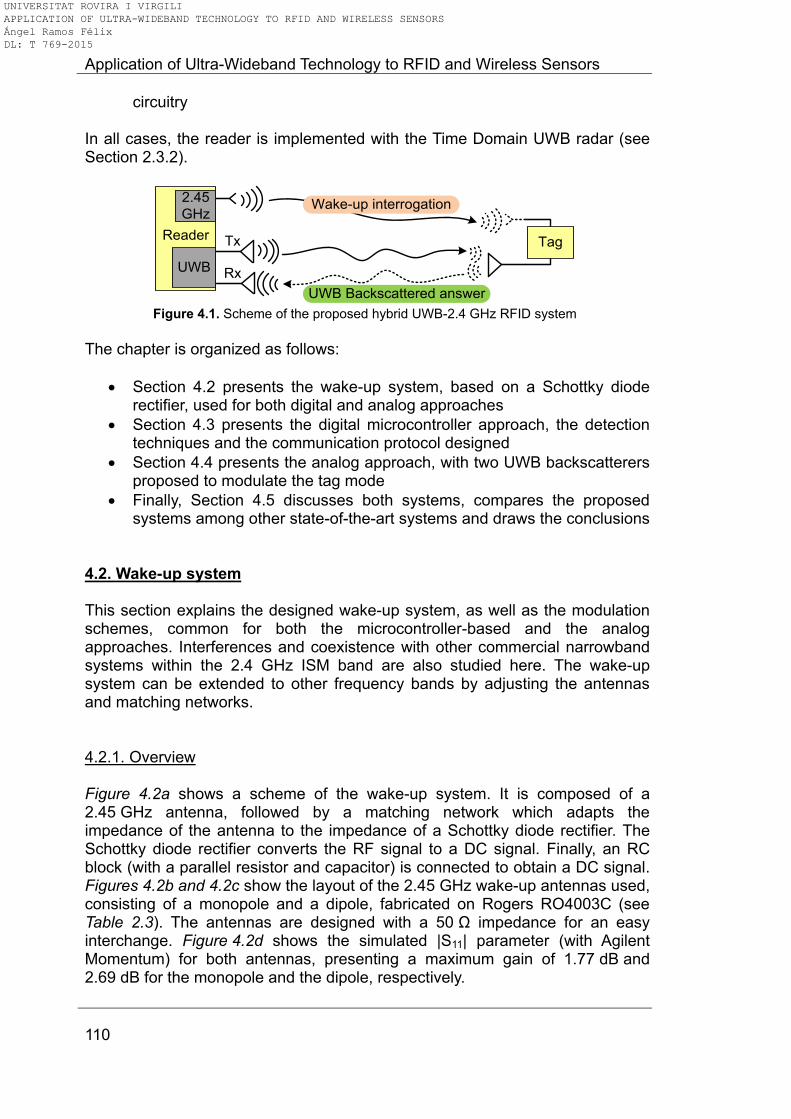
Application of Ultra-Wideband Technology to RFID and Wireless Sensors
110
circuitry In all cases, the reader is implemented with the Time Domain UWB radar (see Section 2.3.2).
Wake-up interrogation2.45
GHz
UWB
UWB Backscattered answer
Reader Tx
Rx
Tag
Figure 4.1. Scheme of the proposed hybrid UWB-2.4 GHz RFID system
The chapter is organized as follows:
Section 4.2 presents the wake-up system, based on a Schottky diode rectifier, used for both digital and analog approaches
Section 4.3 presents the digital microcontroller approach, the detection techniques and the communication protocol designed
Section 4.4 presents the analog approach, with two UWB backscatterers proposed to modulate the tag mode
Finally, Section 4.5 discusses both systems, compares the proposed systems among other state-of-the-art systems and draws the conclusions
4.2. Wake-up system This section explains the designed wake-up system, as well as the modulation schemes, common for both the microcontroller-based and the analog approaches. Interferences and coexistence with other commercial narrowband systems within the 2.4 GHz ISM band are also studied here. The wake-up system can be extended to other frequency bands by adjusting the antennas and matching networks. 4.2.1. Overview Figure 4.2a shows a scheme of the wake-up system. It is composed of a 2.45 GHz antenna, followed by a matching network which adapts the impedance of the antenna to the impedance of a Schottky diode rectifier. The Schottky diode rectifier converts the RF signal to a DC signal. Finally, an RC block (with a parallel resistor and capacitor) is connected to obtain a DC signal. Figures 4.2b and 4.2c show the layout of the 2.45 GHz wake-up antennas used, consisting of a monopole and a dipole, fabricated on Rogers RO4003C (see Table 2.3). The antennas are designed with a 50 Ω impedance for an easy interchange. Figure 4.2d shows the simulated |S11| parameter (with Agilent Momentum) for both antennas, presenting a maximum gain of 1.77 dB and 2.69 dB for the monopole and the dipole, respectively.
UNIVERSITAT ROVIRA I VIRGILI APPLICATION OF ULTRA-WIDEBAND TECHNOLOGY TO RFID AND WIRELESS SENSORS Ángel Ramos Félix DL: T 769-2015
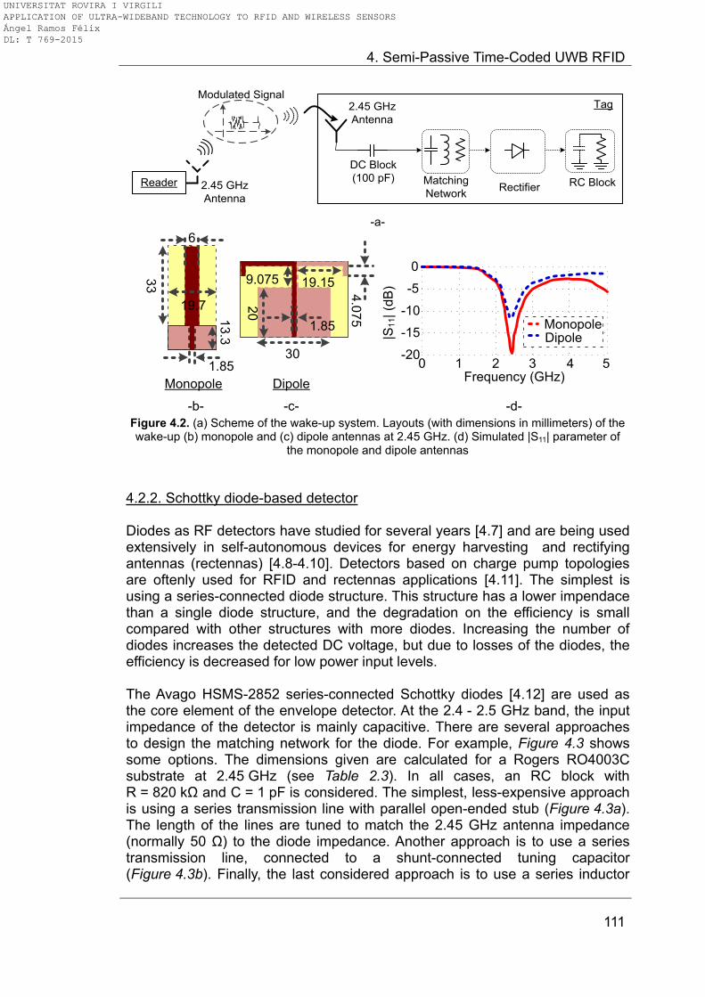
4. Semi-Passive Time-Coded UWB RFID
111
Matching
NetworkRectifier
2.45 GHz
Antenna
RC Block2.45 GHz
Antenna
Reader
Modulated SignalTag
DC Block
(100 pF)
-a-
|S11| (d
B)
0
-5
-10
-15
-200 1 2 3 4 5
Frequency (GHz)1.85
13
.3
33
19.7
6
1.85
20
19.15
30
9.075
4.0
75
MonopoleDipole
Monopole Dipole
-b- -c- -d- Figure 4.2. (a) Scheme of the wake-up system. Layouts (with dimensions in millimeters) of the wake-up (b) monopole and (c) dipole antennas at 2.45 GHz. (d) Simulated |S11| parameter of
the monopole and dipole antennas
4.2.2. Schottky diode-based detector Diodes as RF detectors have studied for several years [4.7] and are being used extensively in self-autonomous devices for energy harvesting and rectifying antennas (rectennas) [4.8-4.10]. Detectors based on charge pump topologies are oftenly used for RFID and rectennas applications [4.11]. The simplest is using a series-connected diode structure. This structure has a lower impendace than a single diode structure, and the degradation on the efficiency is small compared with other structures with more diodes. Increasing the number of diodes increases the detected DC voltage, but due to losses of the diodes, the efficiency is decreased for low power input levels. The Avago HSMS-2852 series-connected Schottky diodes [4.12] are used as the core element of the envelope detector. At the 2.4 - 2.5 GHz band, the input impedance of the detector is mainly capacitive. There are several approaches to design the matching network for the diode. For example, Figure 4.3 shows some options. The dimensions given are calculated for a Rogers RO4003C substrate at 2.45 GHz (see Table 2.3). In all cases, an RC block with R = 820 kΩ and C = 1 pF is considered. The simplest, less-expensive approach is using a series transmission line with parallel open-ended stub (Figure 4.3a). The length of the lines are tuned to match the 2.45 GHz antenna impedance (normally 50 Ω) to the diode impedance. Another approach is to use a series transmission line, connected to a shunt-connected tuning capacitor (Figure 4.3b). Finally, the last considered approach is to use a series inductor
UNIVERSITAT ROVIRA I VIRGILI APPLICATION OF ULTRA-WIDEBAND TECHNOLOGY TO RFID AND WIRELESS SENSORS Ángel Ramos Félix DL: T 769-2015
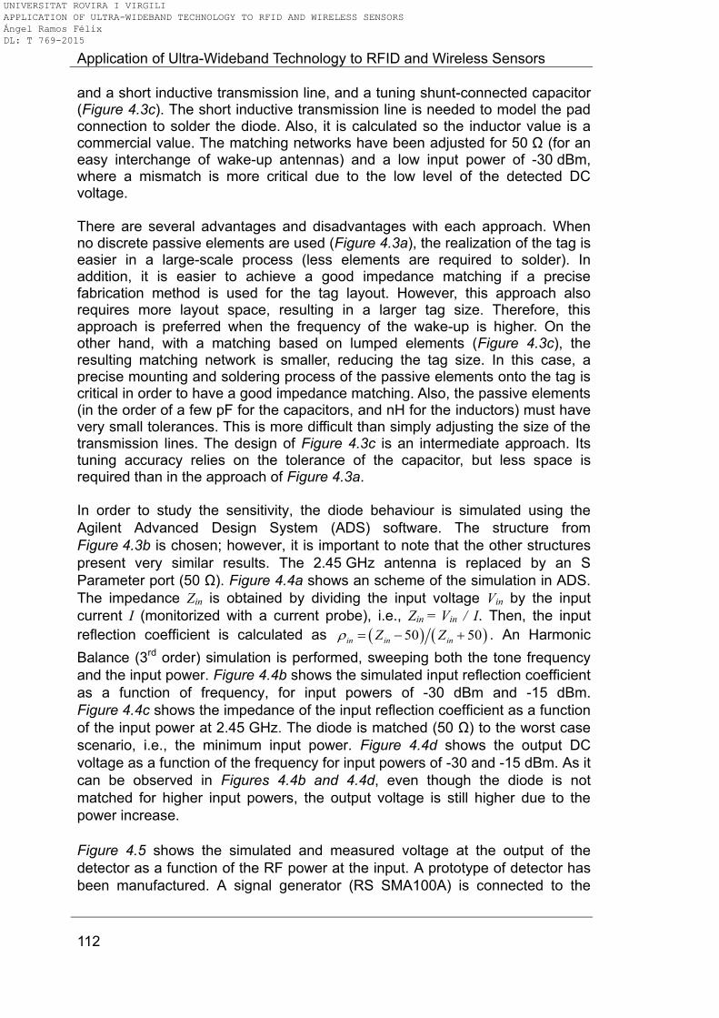
Application of Ultra-Wideband Technology to RFID and Wireless Sensors
112
and a short inductive transmission line, and a tuning shunt-connected capacitor (Figure 4.3c). The short inductive transmission line is needed to model the pad connection to solder the diode. Also, it is calculated so the inductor value is a commercial value. The matching networks have been adjusted for 50 Ω (for an easy interchange of wake-up antennas) and a low input power of -30 dBm, where a mismatch is more critical due to the low level of the detected DC voltage. There are several advantages and disadvantages with each approach. When no discrete passive elements are used (Figure 4.3a), the realization of the tag is easier in a large-scale process (less elements are required to solder). In addition, it is easier to achieve a good impedance matching if a precise fabrication method is used for the tag layout. However, this approach also requires more layout space, resulting in a larger tag size. Therefore, this approach is preferred when the frequency of the wake-up is higher. On the other hand, with a matching based on lumped elements (Figure 4.3c), the resulting matching network is smaller, reducing the tag size. In this case, a precise mounting and soldering process of the passive elements onto the tag is critical in order to have a good impedance matching. Also, the passive elements (in the order of a few pF for the capacitors, and nH for the inductors) must have very small tolerances. This is more difficult than simply adjusting the size of the transmission lines. The design of Figure 4.3c is an intermediate approach. Its tuning accuracy relies on the tolerance of the capacitor, but less space is required than in the approach of Figure 4.3a. In order to study the sensitivity, the diode behaviour is simulated using the
Agilent Advanced Design System (ADS) software. The structure from
Figure 4.3b is chosen; however, it is important to note that the other structures
present very similar results. The 2.45 GHz antenna is replaced by an S
Parameter port (50 Ω). Figure 4.4a shows an scheme of the simulation in ADS.
The impedance Zin is obtained by dividing the input voltage Vin by the input
current I (monitorized with a current probe), i.e., Zin = Vin / I. Then, the input
reflection coefficient is calculated as 50 50in in inZ Z . An Harmonic
Balance (3rd order) simulation is performed, sweeping both the tone frequency
and the input power. Figure 4.4b shows the simulated input reflection coefficient
as a function of frequency, for input powers of -30 dBm and -15 dBm.
Figure 4.4c shows the impedance of the input reflection coefficient as a function
of the input power at 2.45 GHz. The diode is matched (50 Ω) to the worst case
scenario, i.e., the minimum input power. Figure 4.4d shows the output DC
voltage as a function of the frequency for input powers of -30 and -15 dBm. As it
can be observed in Figures 4.4b and 4.4d, even though the diode is not
matched for higher input powers, the output voltage is still higher due to the
power increase.
Figure 4.5 shows the simulated and measured voltage at the output of the
detector as a function of the RF power at the input. A prototype of detector has
been manufactured. A signal generator (RS SMA100A) is connected to the
UNIVERSITAT ROVIRA I VIRGILI APPLICATION OF ULTRA-WIDEBAND TECHNOLOGY TO RFID AND WIRELESS SENSORS Ángel Ramos Félix DL: T 769-2015

4. Semi-Passive Time-Coded UWB RFID
113
input, and a multimeter (Agilent 34410A) is connected to the output in order to
measure voltage. The discrepances at high input power are due to the internal
model used in the simulator, which does not take into account accurately the
breakdown effects in the diode current. The detected voltage is limited by the
diode noise for low input power. Low input powers as small as -65 dBm can be
detected according with the tangential sensitivity reported in the literature for
similar zero bias devices [4.13]. A very good agreement between the simulated
and the measured results can be observed. Theoretically, the reader would be
able to wake-up the tag at a distance of 12.6 m in freespace. This can be
calculated considering an EIRP of +20 dBm output power, a wake-up antenna
of 0 dBi in the tag, and a +3 mV threshold. The 3 mV threshold has been
chosen because it is a typical noise supply level in digital lines.
7 m
m
9.4 mm
1 mm
1 mm
15.7 mm
Microstrip Transmission Line
-a-
2.45 GHz
Antenna
DC Block
(100 pF)
HSMS-
2852
1 p
F
820 k
Ω
2.45 GHz
Antenna
DC Block
(100 pF)
HSMS-
2852
1 p
F
820 k
Ω
13.6
mm
1 mm
Tuning Cap.
(4 pF)
-b-
2.45 GHz
Antenna
DC Block
(100 pF)
HSMS-
2852
1 p
F
820 k
Ω
-c-
3.3 pF
5.6 nH
2.8
mm
0.5 mm
Figure 4.3. Approaches for the matching network. (a) Series transmission line with a parallel
open-ended stub. (b) Series transmission line with shunt-connected tuning capacitor. (c) Series inductor with short inductive transmission line, and shunt-connected tuning capacitor. In red,
elements tuned to achieve a matching at the desired frequency
4.2.3. Reader. Modulation schemes The wake-up part in the reader is realized by means of a voltage controlled oscillator (VCO). Specifically, a 2.45 GHz VCO (Mini-Circuits ROS 2793-119+). This oscillator sends a single-tone through a 2.45 GHz antenna. An On-Off keying (OOK) modulation is obtained by turning on/off the VCO power supply. A Mini-Circuits GAL-84+ medium power amplifier is connected at the output of the VCO. The transmitted power is +20 dBm and a monopole
UNIVERSITAT ROVIRA I VIRGILI APPLICATION OF ULTRA-WIDEBAND TECHNOLOGY TO RFID AND WIRELESS SENSORS Ángel Ramos Félix DL: T 769-2015
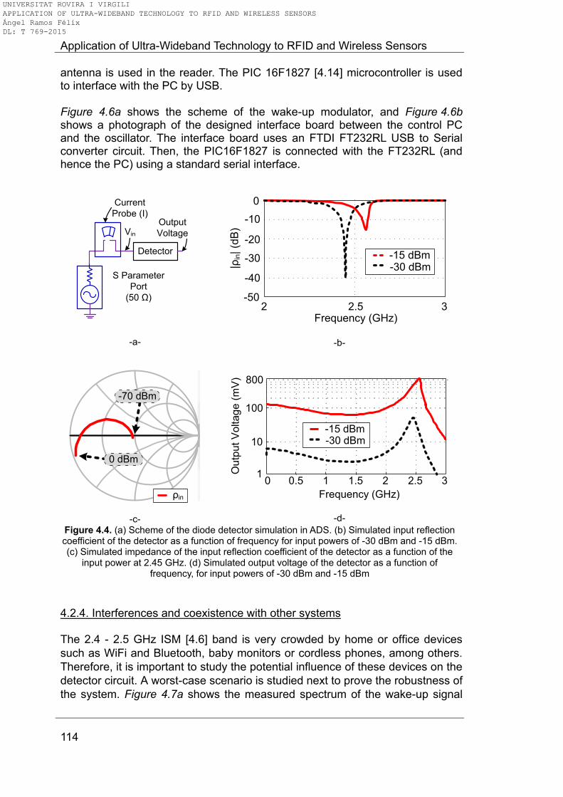
Application of Ultra-Wideband Technology to RFID and Wireless Sensors
114
antenna is used in the reader. The PIC 16F1827 [4.14] microcontroller is used to interface with the PC by USB. Figure 4.6a shows the scheme of the wake-up modulator, and Figure 4.6b shows a photograph of the designed interface board between the control PC and the oscillator. The interface board uses an FTDI FT232RL USB to Serial converter circuit. Then, the PIC16F1827 is connected with the FT232RL (and hence the PC) using a standard serial interface.
S Parameter
Port
(50 Ω)
Current
Probe (I)
Vin
Detector
Output
Voltage
-a-
Frequency (GHz)2 2.5 3
-15 dBm-30 dBm
0
-10
-20
-30
-40
-50
|ρin| (d
B)
-b-
-70 dBm
0 dBm
ρin
-c-
0.5 1 1.5 2 2.50 3
Frequency (GHz)
Outp
ut
Voltag
e (
mV
) 800
100
10
1
-15 dBm-30 dBm
-d-
Figure 4.4. (a) Scheme of the diode detector simulation in ADS. (b) Simulated input reflection coefficient of the detector as a function of frequency for input powers of -30 dBm and -15 dBm. (c) Simulated impedance of the input reflection coefficient of the detector as a function of the
input power at 2.45 GHz. (d) Simulated output voltage of the detector as a function of frequency, for input powers of -30 dBm and -15 dBm
4.2.4. Interferences and coexistence with other systems The 2.4 - 2.5 GHz ISM [4.6] band is very crowded by home or office devices
such as WiFi and Bluetooth, baby monitors or cordless phones, among others.
Therefore, it is important to study the potential influence of these devices on the
detector circuit. A worst-case scenario is studied next to prove the robustness of
the system. Figure 4.7a shows the measured spectrum of the wake-up signal
UNIVERSITAT ROVIRA I VIRGILI APPLICATION OF ULTRA-WIDEBAND TECHNOLOGY TO RFID AND WIRELESS SENSORS Ángel Ramos Félix DL: T 769-2015
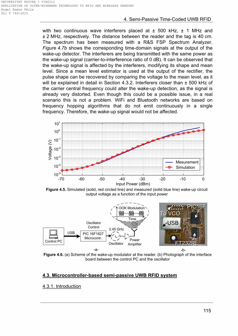
4. Semi-Passive Time-Coded UWB RFID
115
with two continuous wave interferers placed at ± 500 kHz, ± 1 MHz and
± 2 MHz, respectively. The distance between the reader and the tag is 40 cm.
The spectrum has been measured with a R&S FSP Spectrum Analyzer.
Figure 4.7b shows the corresponding time-domain signals at the output of the
wake-up detector. The interferers are being transmitted with the same power as
the wake-up signal (carrier-to-interference ratio of 0 dB). It can be observed that
the wake-up signal is affected by the interferers, modifying its shape and mean
level. Since a mean level estimator is used at the output of the rectifier, the
pulse shape can be recovered by comparing the voltage to the mean level, as it
will be explained in detail in Section 4.3.2. Interferers closer than ± 500 kHz of
the carrier central frequency could alter the wake-up detection, as the signal is
already very distorted. Even though this could be a possible issue, in a real
scenario this is not a problem. WiFi and Bluetooth networks are based on
frequency hopping algorithms that do not emit continuously in a single
frequency. Therefore, the wake-up signal would not be affected.
-70 -60 -50 -40 -30 -20 -10 0
101
Input Power (dBm)
Vo
lta
ge
(V
)
100
10-1
10-2
10-3
10-4
10-5
Mesurement
Simulation
Figure 4.5. Simulated (solid, red circled line) and measured (solid blue line) wake-up circuit
output voltage as a function of the input power
OOK Modulation
Oscillator
USB
TimeOscillator
Control
PIC 16F1827
Microcontr.Power
Amplifier
2.45 GHz
Control PC
-a-
USB
FT232RLFT232RL
PIC16FPIC16F
To VCOTo VCO
-b-
Figure 4.6. (a) Scheme of the wake-up modulator at the reader. (b) Photograph of the interface board between the control PC and the oscillator
4.3. Microcontroller-based semi-passive UWB RFID system 4.3.1. Introduction
UNIVERSITAT ROVIRA I VIRGILI APPLICATION OF ULTRA-WIDEBAND TECHNOLOGY TO RFID AND WIRELESS SENSORS Ángel Ramos Félix DL: T 769-2015
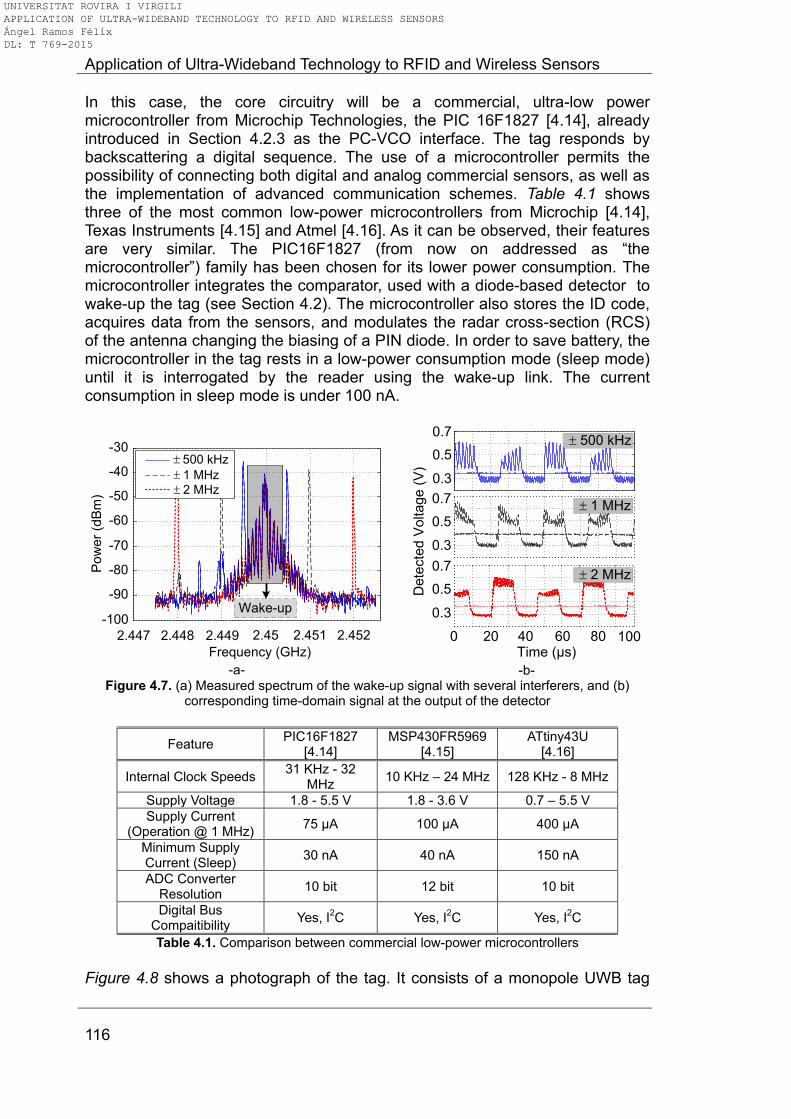
Application of Ultra-Wideband Technology to RFID and Wireless Sensors
116
In this case, the core circuitry will be a commercial, ultra-low power microcontroller from Microchip Technologies, the PIC 16F1827 [4.14], already introduced in Section 4.2.3 as the PC-VCO interface. The tag responds by backscattering a digital sequence. The use of a microcontroller permits the possibility of connecting both digital and analog commercial sensors, as well as the implementation of advanced communication schemes. Table 4.1 shows three of the most common low-power microcontrollers from Microchip [4.14], Texas Instruments [4.15] and Atmel [4.16]. As it can be observed, their features are very similar. The PIC16F1827 (from now on addressed as “the microcontroller”) family has been chosen for its lower power consumption. The microcontroller integrates the comparator, used with a diode-based detector to wake-up the tag (see Section 4.2). The microcontroller also stores the ID code, acquires data from the sensors, and modulates the radar cross-section (RCS) of the antenna changing the biasing of a PIN diode. In order to save battery, the microcontroller in the tag rests in a low-power consumption mode (sleep mode) until it is interrogated by the reader using the wake-up link. The current consumption in sleep mode is under 100 nA.
-100
-90
-80
-70
-60
-50
-40
-30
Pow
er
(dB
m)
2.447 2.448 2.449 2.45 2.451 2.452
Frequency (GHz)
500 kHz
1 MHz 2 MHz
Wake-up
-a-
0.3
0.5
0.7
0Time (μs)
0.3
0.5
0.7
De
tecte
d V
olta
ge
(V
)
0.3
0.5
0.7 2 MHz
1 MHz
500 kHz
20 40 60 80 100
-b-
Figure 4.7. (a) Measured spectrum of the wake-up signal with several interferers, and (b) corresponding time-domain signal at the output of the detector
Feature PIC16F1827
[4.14] MSP430FR5969
[4.15] ATtiny43U
[4.16]
Internal Clock Speeds 31 KHz - 32
MHz 10 KHz – 24 MHz 128 KHz - 8 MHz
Supply Voltage 1.8 - 5.5 V 1.8 - 3.6 V 0.7 – 5.5 V
Supply Current (Operation @ 1 MHz)
75 μA 100 μA 400 μA
Minimum Supply Current (Sleep)
30 nA 40 nA 150 nA
ADC Converter Resolution
10 bit 12 bit 10 bit
Digital Bus Compaitibility
Yes, I2C Yes, I
2C Yes, I
2C
Table 4.1. Comparison between commercial low-power microcontrollers
Figure 4.8 shows a photograph of the tag. It consists of a monopole UWB tag
UNIVERSITAT ROVIRA I VIRGILI APPLICATION OF ULTRA-WIDEBAND TECHNOLOGY TO RFID AND WIRELESS SENSORS Ángel Ramos Félix DL: T 769-2015
4. Semi-Passive Time-Coded UWB RFID
117
(see Section 2.6.2) loaded with a PIN diode, and the 2.45 GHz detector from
Figure 4.3c connected to the 2.45 GHz monopole antenna presented in
Section 4.2.1. Both are connected to the microcontroller, which is powered
using a 3 V Lithium battery. The tag size is 70.93 mm x 50.97 mm and it is
fabricated on a Rogers RO4003C substrate (see Table 2.3).
UWB Backscatterer
PIC
PIN Diode
Program. pins
UWB
Antenna
Delay Line
70.93 mm
Detector2.45 GHz
Antenna
2.45 GHz
Detector
50.9
7 m
m
-a-
2.45 GHz
Antenna
Programming
pins (PIC)
Battery
UWB
Antenna
-b-
Figure 4.8. Photograph of the designed tag, top face (a) and bottom face (b)
4.3.2. Microcontroller: tag core logic To minimize the tag size, the rectifier is realized using the approach of mainly
passive elements (see Section 4.2.2), and its circuit is shown in Figure 4.9a.
The rectifier output is connected to the negative input of the microcontroller
(“Data”) internal comparator, as shown in Figure 4.9b. The threshold voltage for
this comparator is generated by a slicing RC circuit (R = 100 kΩ, C = 3 nF) at
the output of the detector. In this way, the threshold automatically adjusts to the
mean value of the detected signal. The comparator generates an interrupt when
the wake-up signal is greater than the threshold voltage, initiating the
microcontroller program. Using an internal comparator increases the tag battery
lifetime, since it avoids additional circuitry that would increase the current
consumption of the tag during sleep periods.
In order to send information from the reader to the tag using the wake-up signal,
a pulse-width modulation (PWM) scheme is used, as it is also shown in
UNIVERSITAT ROVIRA I VIRGILI APPLICATION OF ULTRA-WIDEBAND TECHNOLOGY TO RFID AND WIRELESS SENSORS Ángel Ramos Félix DL: T 769-2015
Application of Ultra-Wideband Technology to RFID and Wireless Sensors
118
Figure 4.9b. Depending on the high level time of the rectified signal a „0‟ or a „1‟
bit is considered. A 33% of the period at a high level codes a „0‟, and a 66%
codes a „1‟. In this prototype, the period of the PWM signal for each bit is set to
25 μs, meaning a speed of 40 Kbps. This speed is enough for the amount of
information that a RFID reader needs to send (mainly interrogation requests
and configuration commands). The microcontroller program clock frequency has
been set to a reduced value (1 MHz) to minimize the tag power consumption.
One of the main advantages of this topology is that the reader controls the tag
clock using the wake-up link, and there is not a pulse generator in the tag.
Therefore, there is no need for a synchronization method between the reader
and the tag clocks, as it was performed in [4.17].
DC Block
(100 pF)3.3 pF
5.6 nH L = 2.8 mm
W= 0.5 mm
Avago
HSMS-2852
Impedance
Matching
Network
1 pF 820 kΩ
Rectified
signal
To Negative Input
Schottky
Diode
2.45 GHz
2.45 GHz
Antenna
Mean rectified
signal
100 kΩ
3 nF
To Positive Input
-a-
Rectified Wake-up Signal
C1
Comp.
-+
Interrupt
PIC 16F1827
„0‟mV
„1‟
8.33 25
μs16.67 25
mV
To PIN Diode
UWB Backscatterer
DAC
„0‟ (0.7 V)
„1‟ (3.0 V)
μs
Data
Thre
sho
ld
(Mean
)
-b-
Figure 4.9. (a) Scheme of the 2.45 GHz wake-up detector circuit with microcontroller. (b) Scheme of the wake-up signal for „0‟ and „1‟ cases and their detection using the microcontroller
internal comparator
4.3.3. UWB backscatterer design and evaluation The backscatterer is composed of a UWB antenna connected to a delay line of
length L and characteristic impedance Zc. In Section 2.2, a two-port circuit
model is used to explain the time-domain signal scattered by a UWB antenna
connected to a transmission line. Here, the delay line is loaded with a PIN diode
(NXP Semiconductors BAP51-03) [4.18] biased through a 33 kΩ resistor. It is
shown in Figure 4.10a. The bias of the PIN diode is controlled by the
microcontroller, implementing a logical „1‟ when the diode is ON and a logical „0‟
when it is OFF.
UNIVERSITAT ROVIRA I VIRGILI APPLICATION OF ULTRA-WIDEBAND TECHNOLOGY TO RFID AND WIRELESS SENSORS Ángel Ramos Félix DL: T 769-2015
4. Semi-Passive Time-Coded UWB RFID
119
Figure 4.10b shows a scheme of the transmitted (Tx) and received (Rx) signals
at the reader. The transmission line connected to the tag‟s antenna (see
Section 2.2) is now ended with a PIN diode. The microcontroller sends a „0‟ or
„1‟ signal by setting the output voltage to a low (0.7 V, instead of 0 V, will be
explained next) or high (3 V) level respectively. This way, the PIN diode is
biased from an open circuit (ΓLOAD = 1) to a short circuit (ΓLOAD = -1), depending
on the current that flows through it. Therefore, the „0‟ and „1‟ states will have tag
modes with opposite phases.
S1
1a
S2
2a
S21a
S12a
Incoming
wave
IN
UWB
Antenna
L
(Zc)
LOAD
L
PIN Diode
(BAP51-03)
Transmission Line
Bias
Resistor
Outcoming
waveModel
From Tag Chip:
0.7 V („0‟)
3.0 V („1‟)
-a-
UWB
Backscatterer
Time
Time
2L/v
Transmitted
Signal
Coupling
Backscattered
signal
Modulated
Tag Mode
„0‟
„1‟
Structural
Mode
Tag
Tx, p(t)
Rx, s(t)
-b-
Figure 4.10. (a) Model of the modulated backscattering UWB PIN-loaded antenna. (b) Scheme of the transmitted and backscattered UWB signals
In order to study the time-domain response of the BAP51-03 PIN diode, a characterization board has been designed. It is shown in Figure 4.11a. It consists of a microstrip transmission line fabricated on Rogers 4003C substrate. The transmission line is terminated with the PIN diode. Some extra pads are also added to solder a polarization resistor and the power supply wires to polarize the diode. The reflection coefficient is measured between 0.1 and 10 GHz with 1601 points using the Agilent E8364C network analyzer (VNA). In order to calibrate the VNA at the same plane where the PIN diode is soldered, a custom calibration kit (shown also in Figure 4.11a) is used to perform an open-short-load (OSL) calibration [4.19]. A 33 kΩ 0603 surface mount (SMD) resistor is used to bias the diode, actuating as a broadband RF block. An Agilent 34410A multimeter is connected in series with a programmable DC power source for current monitoring. Figure 4.11b shows the diode resistance as a function of the forward current from the diode datasheet. According to the diode
UNIVERSITAT ROVIRA I VIRGILI APPLICATION OF ULTRA-WIDEBAND TECHNOLOGY TO RFID AND WIRELESS SENSORS Ángel Ramos Félix DL: T 769-2015

Application of Ultra-Wideband Technology to RFID and Wireless Sensors
120
datasheet, a current greater than 500 μA would be necessary to achieve a short-circuit state. Figure 4.11c shows the time-domain response (after applying the inverse Fourier transform to the VNA acquired signal) of the calibrated S11 parameter of the diode for several diode forward currents IF. It can be seen that the pulse is inverted (meaning a ±180º change of phase) for forward currents equal or greater than 30 μA. This is due to the change in the reflection coefficient introduced by the diode, from an open circuit to a short circuit. It can be observed that when biasing the diode with just 30 μA the phase change is perfectly detected. Moreover, for forward currents greater than 130 μA the amplitude values start to saturate, since the reflection coefficients are similar. Therefore, it is proved that this diode can be used to change the reflection coefficient of a load at UWB frequencies, and a current of 500 μA is not required.
Open Load Short
Calibration Kit
Characterization
Board
-a-
500 600 700 800 900 1000
3.5
4
4.5
5
5.5
Dio
de R
esis
tance (
Ω)
IF (μA)
-b-
0 0.1 0.2 0.3 0.4 0.5 0.6 0.7 0.8 0.9 1-1
-0.75
-0.5
-0.25
0
0.25
0.5
0.75
1
Time (ns)
No
rma
lize
d A
mp
litu
de
0 30130230330430530630730830930
Diode Forward
Current, IF (μA)IF = 0 μA
IF = 30 μA
IF > 130 μA
-c-
Figure 4.11. (a) Characterization board and custom calibration kit for the PIN diode. (b) Diode resistance as a function of the forward current, according to the manufacturer‟s datasheet. (c) Time-domain response of the S11 parameter of the diode for forward currents from 0 to 930 μA
Using the Time Domain radar, the tag is read at a fixed 50 cm distance for different diode forward currents. The background subtraction technique and the time-windowing technique from Section 2.4.1 are applied to the received signal. Figure 4.12a shows the tag‟s time domain response for PIN diode currents from
UNIVERSITAT ROVIRA I VIRGILI APPLICATION OF ULTRA-WIDEBAND TECHNOLOGY TO RFID AND WIRELESS SENSORS Ángel Ramos Félix DL: T 769-2015
4. Semi-Passive Time-Coded UWB RFID
121
0 to 730 μA. The time delay of the structural modes for all currents remains the same, as expected. The tag modes present an inverted phase when the forward current is greater than 0 μA. There is a small difference between the 30 μA and the > 130 μA states due to the change in the resistance when the forward current increases. For currents greater than 130 μA the difference is not noticeable. A forward current of 70 μA is chosen for the „1‟ state. This is to achieve a compromise between consumption and performance. In all cases from Figure 4.12a it can be seen that the amplitude of the tag mode also changes when biasing the diode. When the diode current increases, the diode resistance decreases. Then, the magnitude of the reflection coefficient increases, resulting in an increase of the tag mode amplitude. Ideally, the maximum would correspond to a short circuit. Figure 4.12b shows the measured tag-to-structural mode ratio for currents from 0 to 70 μA. It corresponds to the tag mode peak amplitude over the structural mode peak amplitude. It can be observed that the maximum amplitude difference for two diode currents is achieved with a forward current of 5 μA for the „0‟ state. Therefore, the „0‟ state is generated by biasing the diode with 0.7 V with the 33 kΩ bias resistor (see Figure 4.9). The state change, therefore, can be detected as an amplitude change rather than as a phase change, permitting the use of the Wavelet processing technique (see Section 2.4.2). It will be addressed in detail in Section 4.3.7. 4.3.4. Differential coding and detection techniques Instead of subtracting the same empty-room background scenario from all signals, an alternate technique is proposed for the digital tag. As explained in Section 2.4.1, the background subtraction eliminates clutter assuming that it does not change in time. In addition, it is assumed that the structural and tag modes have a finite time duration and the delay between the two signals introduced by the delay line is enough to separate them. However, from the previous results in Chapters 2 and 3 a residual interference between the two modes can be observed. In order to reduce this interference, the length of the delay line should be increased, resulting in a large tag size and a reduction of tag mode amplitude due to the transmission line losses. To solve this problem, a differential coding schema has been adopted. For each measured RAW signal si(t), the differential signal di-1(t) is:
1 1( ) ( ) ( )i i id t s t s t , (4.1)
where i = 2,3,...,n (n is the number of bits in a frame) and si-1(t) is the preceeding RAW signal corresponding to the measured previous state. In this manner, the difference between one state and its preceeding one is obtained. From the chipless theoretical expressions in Section 2.2 it can be seen that the structural mode will be cancelled because it does not change with the load or state. Also, the clutter is considerably reduced, assuming that it does not change between one bit and another. For two consecutive identical states, i.e., two „0‟ or two „1‟
UNIVERSITAT ROVIRA I VIRGILI APPLICATION OF ULTRA-WIDEBAND TECHNOLOGY TO RFID AND WIRELESS SENSORS Ángel Ramos Félix DL: T 769-2015
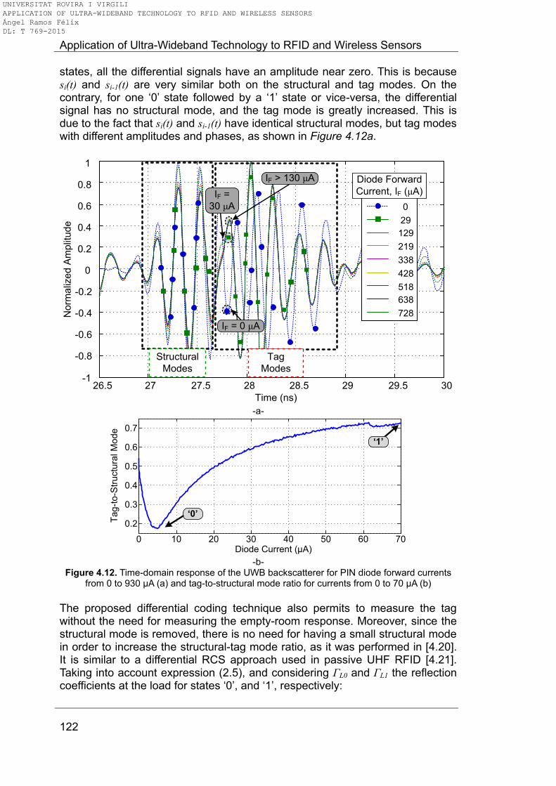
Application of Ultra-Wideband Technology to RFID and Wireless Sensors
122
states, all the differential signals have an amplitude near zero. This is because si(t) and si-1(t) are very similar both on the structural and tag modes. On the contrary, for one „0‟ state followed by a „1‟ state or vice-versa, the differential signal has no structural mode, and the tag mode is greatly increased. This is due to the fact that si(t) and si-1(t) have identical structural modes, but tag modes with different amplitudes and phases, as shown in Figure 4.12a.
-1
-0.8
-0.6
-0.4
-0.2
0
0.2
0.4
0.6
0.8
1
Norm
aliz
ed
Am
plit
ud
e
26.5 27 27.5 28 28.5 29 29.5 30
Time (ns)
0
29
129
219
338
428
518
638
728
Diode Forward
Current, IF (μA)
Structural
Modes
Tag
Modes
IF = 0 μA
IF =
30 μA
IF > 130 μA
-a-
0 10 20 30 40 50 60 70
0.2
0.3
0.4
0.5
0.6
0.7
Diode Current (μA)
Tag-t
o-S
tructu
ral M
od
e
‘0’
‘1’
-b-
Figure 4.12. Time-domain response of the UWB backscatterer for PIN diode forward currents from 0 to 930 μA (a) and tag-to-structural mode ratio for currents from 0 to 70 μA (b)
The proposed differential coding technique also permits to measure the tag without the need for measuring the empty-room response. Moreover, since the structural mode is removed, there is no need for having a small structural mode in order to increase the structural-tag mode ratio, as it was performed in [4.20]. It is similar to a differential RCS approach used in passive UHF RFID [4.21]. Taking into account expression (2.5), and considering ΓL0 and ΓL1 the reflection coefficients at the load for states „0‟, and „1‟, respectively:
UNIVERSITAT ROVIRA I VIRGILI APPLICATION OF ULTRA-WIDEBAND TECHNOLOGY TO RFID AND WIRELESS SENSORS Ángel Ramos Félix DL: T 769-2015

4. Semi-Passive Time-Coded UWB RFID
123
0 11 21 12 0in a a a LS S S , (4.2)
1 11 21 12 1in a a a LS S S , (4.3)
and, the differential reflection coefficient at the input of the tag can be computed as:
0 1 21 12 0 1in in in a a L LS S , (4.4)
where S12a S21a can be interpreted as the tag‟s antenna gain. The differential signal has a tag mode. Therefore, the Continuous Wavelet Transform technique can be applied to improve the signal to noise ratio, as performed in Section 2.4.1. To distinguish whether there is or not a state change, a threshold must be considered to compare with the maximum peak amplitudes. Theoretically, a fixed value of 0.5 should be considered for the threshold. The “non-changed” states have amplitude near 0, and the “changed” states have amplitude near 1. However, in practice, this threshold must be variable. Random noise and propagation can produce differences between two identical bits. For an 8-bit sequence, the CWT of the differential signal is calculated, and then the maximum peaks are obtained. These peaks are classified as “non-changed” or “changed” with a threshold of 0.5. Then, the variable threshold Th is calculated as:
1
2Th NonChg Chg , (4.5)
where NonChg and Chg are the mean values of the “non-changed” and
“changed” states, respectively, for a frame. Figure 4.13 shows a constellation
diagram for the “non-changed” and “changed” states. It can be interpreted as an
amplitude shift keying (ASK) modulation with a variable threshold.
Normalized
Amplitude
Th ChgNonChg
10
Figure 4.13. Constellation diagram for the "changed" and "non-changed" states at the tag after
differential signal
4.3.5. Communication protocol The communication protocol between reader and sensor consists of four main
UNIVERSITAT ROVIRA I VIRGILI APPLICATION OF ULTRA-WIDEBAND TECHNOLOGY TO RFID AND WIRELESS SENSORS Ángel Ramos Félix DL: T 769-2015
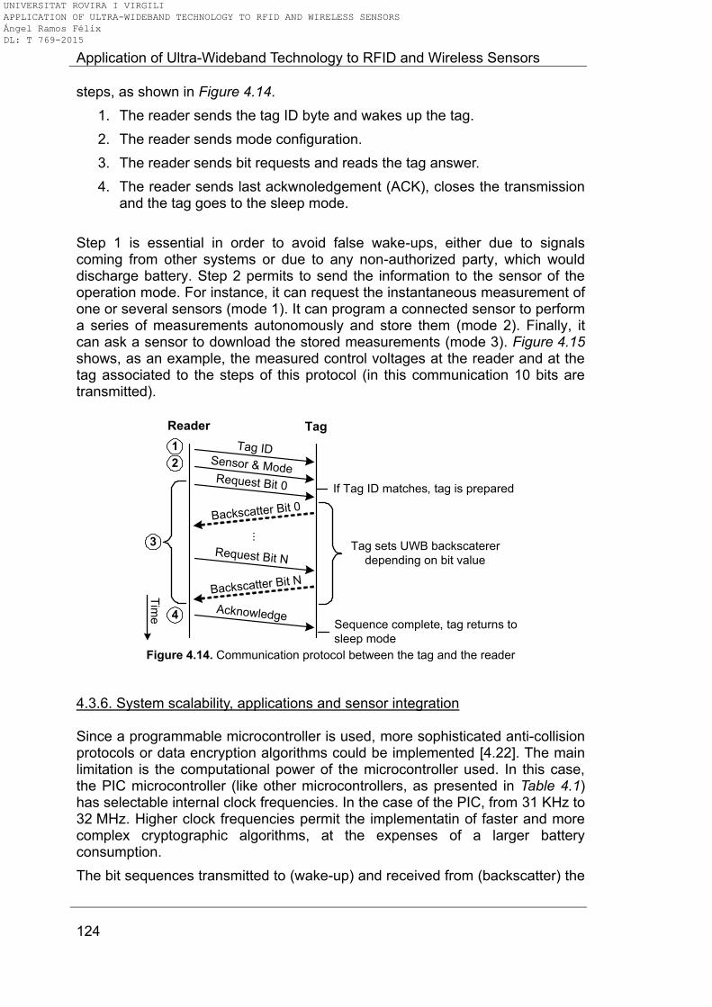
Application of Ultra-Wideband Technology to RFID and Wireless Sensors
124
steps, as shown in Figure 4.14.
1. The reader sends the tag ID byte and wakes up the tag.
2. The reader sends mode configuration.
3. The reader sends bit requests and reads the tag answer.
4. The reader sends last ackwnoledgement (ACK), closes the transmission and the tag goes to the sleep mode.
Step 1 is essential in order to avoid false wake-ups, either due to signals coming from other systems or due to any non-authorized party, which would discharge battery. Step 2 permits to send the information to the sensor of the operation mode. For instance, it can request the instantaneous measurement of one or several sensors (mode 1). It can program a connected sensor to perform a series of measurements autonomously and store them (mode 2). Finally, it can ask a sensor to download the stored measurements (mode 3). Figure 4.15 shows, as an example, the measured control voltages at the reader and at the tag associated to the steps of this protocol (in this communication 10 bits are transmitted).
1
Reader Tag
Tag IDSensor & ModeRequest Bit 0
Backscatter Bit 0
Request Bit N
Backscatter Bit N
...
Acknowledge
If Tag ID matches, tag is prepared
Tag sets UWB backscaterer
depending on bit value
Sequence complete, tag returns to
sleep mode
Tim
e
2
3
4
Figure 4.14. Communication protocol between the tag and the reader
4.3.6. System scalability, applications and sensor integration Since a programmable microcontroller is used, more sophisticated anti-collision protocols or data encryption algorithms could be implemented [4.22]. The main limitation is the computational power of the microcontroller used. In this case, the PIC microcontroller (like other microcontrollers, as presented in Table 4.1) has selectable internal clock frequencies. In the case of the PIC, from 31 KHz to 32 MHz. Higher clock frequencies permit the implementatin of faster and more complex cryptographic algorithms, at the expenses of a larger battery consumption.
The bit sequences transmitted to (wake-up) and received from (backscatter) the
UNIVERSITAT ROVIRA I VIRGILI APPLICATION OF ULTRA-WIDEBAND TECHNOLOGY TO RFID AND WIRELESS SENSORS Ángel Ramos Félix DL: T 769-2015
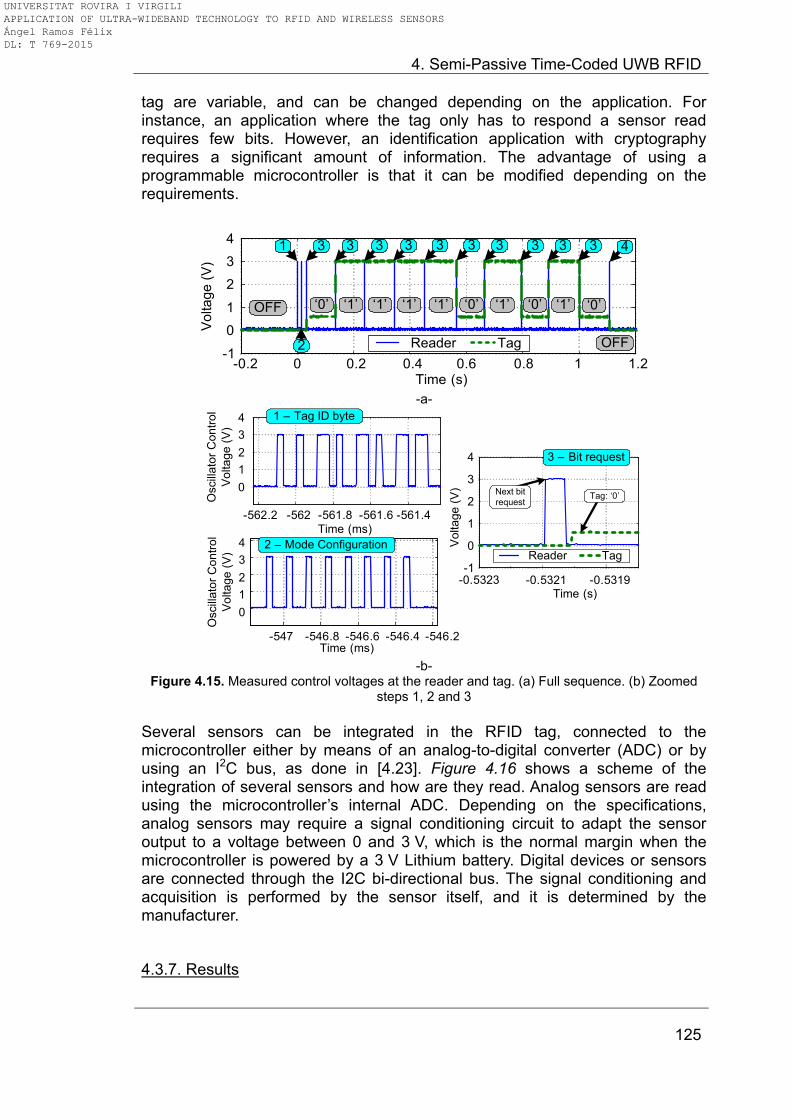
4. Semi-Passive Time-Coded UWB RFID
125
tag are variable, and can be changed depending on the application. For instance, an application where the tag only has to respond a sensor read requires few bits. However, an identification application with cryptography requires a significant amount of information. The advantage of using a programmable microcontroller is that it can be modified depending on the requirements.
-0.2 0 0.2 0.4 0.6 0.8 1 1.2-1
0
1
2
3
4
Time (s)
Vo
lta
ge (
V)
1 3
2
3 3 3 3 3 3 3 3 3 4
„0‟ „1‟ „1‟ „1‟ „1‟ „0‟ „1‟ „1‟„0‟ „0‟
OFF
OFF
Reader Tag
-a-
-562.2 -562 -561.8 -561.6 -561.4
0
1
2
3
4
Time (ms)
Oscill
ato
r C
on
tro
l
Vo
lta
ge (
V)
-547 -546.8 -546.6 -546.4 -546.2Time (ms)
0
1
2
3
4
Oscill
ato
r C
on
tro
l
Volta
ge
(V
)
-0.5323 -0.5321 -0.5319-1
0
1
2
3
4
Time (s)
Volta
ge
(V
)
1 – Tag ID byte
2 – Mode Configuration
3 – Bit request
Next bit
requestTag: „0‟
Reader Tag
-b-
Figure 4.15. Measured control voltages at the reader and tag. (a) Full sequence. (b) Zoomed steps 1, 2 and 3
Several sensors can be integrated in the RFID tag, connected to the microcontroller either by means of an analog-to-digital converter (ADC) or by using an I2C bus, as done in [4.23]. Figure 4.16 shows a scheme of the integration of several sensors and how are they read. Analog sensors are read using the microcontroller‟s internal ADC. Depending on the specifications, analog sensors may require a signal conditioning circuit to adapt the sensor output to a voltage between 0 and 3 V, which is the normal margin when the microcontroller is powered by a 3 V Lithium battery. Digital devices or sensors are connected through the I2C bi-directional bus. The signal conditioning and acquisition is performed by the sensor itself, and it is determined by the manufacturer.
4.3.7. Results
UNIVERSITAT ROVIRA I VIRGILI APPLICATION OF ULTRA-WIDEBAND TECHNOLOGY TO RFID AND WIRELESS SENSORS Ángel Ramos Félix DL: T 769-2015

Application of Ultra-Wideband Technology to RFID and Wireless Sensors
126
To verify the system, the tag sends the sequence “00101011” when the reader interrogates it. The sequence is answered by backscattering: the tag microcontroller biases the PIN diode from 5 to 70 μA. In order to synchronize the tag and the reader, the tag only changes its state (i.e., sends the next bit of the sequence) when the reader sends a wake-up signal, meaning that the reader is ready for the next bit. Figures 4.17a-b show the time-windowed UWB RAW signals for all states obtained with the radar setup at 50 cm. All signals are normalized with respect to the maximum absolute amplitude of all of them. A difference between „0‟ and „1‟ states can be perfectly observed. Figures 4.17c-d show the same signals after applying the background subtraction technique (see Section 2.4). It can be seen that the noise has been reduced, and the difference between „0‟ and „1‟ states is more noticeable.
UWB
Backscatterer
2.45 GHz
Wake -up
Core Logic
PIC 16F 1827
ADCDigital
Device or
Sensor
Conditioning
& Acquisition
I2C
SDA
SCL
Time
+-
Signal
ConditioningAnalog
Sensor 0 V
3 V
Figure 4.16. Integration of sensors in the digital microcontroller-based tag
Since a difference in the signals amplitude between both states is also noticeable, the continuous Wavelet transform is applied to all signals independently. The maximum magnitude cuts of the CWTs are shown in Figure 4.18a. It can be observed that the tag modes for „1‟ states have a greater amplitude than „0‟ states. Finally, Figure 4.18b shows an image of the CWT signals sequence. It can be observed that the states are correctly detected, and the bit sequence can be obtained by the reader. Now, the benefits of the differential signal approach explained in Section 4.3.4 are shown. Figure 4.19 shows the differential signals for the same „00101011‟ sequence. It can be seen that the structural modes are removed by the subtraction of the previous signal for all cases, but the tag modes appear when there is a state change (bit change). Figure 4.20a shows the continuous Wavelet transform of the differential signals
for the same sequence („00101011‟). All signals are normalized with respect to
the absolute maximum of all of them. Since the measurement at 50 cm is very
close to the reader, the dynamic threshold is 0.5016, very close to the
theoretical value of 0.5. Figure 4.20b shows the image sequence of the
differential signals at 50 cm. The state changes occur according to the
sequence the tag is responding.
UNIVERSITAT ROVIRA I VIRGILI APPLICATION OF ULTRA-WIDEBAND TECHNOLOGY TO RFID AND WIRELESS SENSORS Ángel Ramos Félix DL: T 769-2015
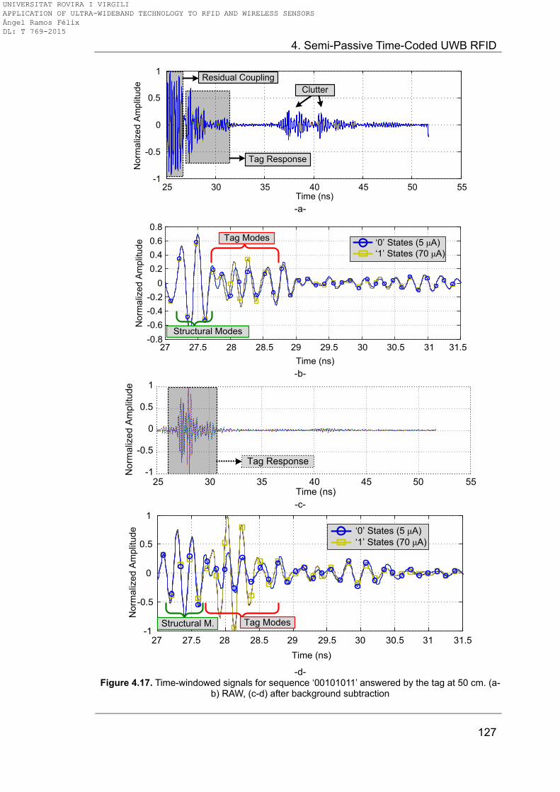
4. Semi-Passive Time-Coded UWB RFID
127
25 30 35 40 45 50 55-1
-0.5
0
0.5
1
Time (ns)
No
rmaliz
ed A
mplit
ude
Residual Coupling
Tag Response
Clutter
-a-
27 27.5 28 28.5 29 29.5 30 30.5 31 31.5-0.8
-0.6
-0.4
-0.2
0
0.2
0.4
0.6
0.8
Time (ns)
No
rma
lize
d A
mp
litu
de „0‟ States (5 μA)
„1‟ States (70 μA)
Structural Modes
Tag Modes
-b-
25 30 35 40 45 50 55-1
-0.5
0
0.5
1
Time (ns)
No
rmaliz
ed A
mplit
ude
Tag Response
-c-
27 27.5 28 28.5 29 29.5 30 30.5 31 31.5-1
-0.5
0
0.5
1
Time (ns)
No
rma
lize
d A
mp
litu
de
Structural M. Tag Modes
„0‟ States (5 μA)
„1‟ States (70 μA)
-d-
Figure 4.17. Time-windowed signals for sequence „00101011‟ answered by the tag at 50 cm. (a-b) RAW, (c-d) after background subtraction
UNIVERSITAT ROVIRA I VIRGILI APPLICATION OF ULTRA-WIDEBAND TECHNOLOGY TO RFID AND WIRELESS SENSORS Ángel Ramos Félix DL: T 769-2015
Application of Ultra-Wideband Technology to RFID and Wireless Sensors
128
0
0.2
No
rmaliz
ed A
mplit
ude
0.4
0.6
0.8
1
25 30 35 40 45 50 55
Time (ns)
26 27 28 29 30 310
0.2
0.4
0.6
0.8
1
Time (ns)
No
rmaliz
ed A
mplit
ude
Structural M. Tag Modes
„0‟ States
„1‟ States
-a-
Tim
e (
ns)
0.10.10.20.20.30.30.40.40.50.50.60.60.70.70.80.80.90.911
00
Bit Number1 2 3 4 5 6 7 8
26
27
28
29
30
31
Structural ModesStructural Modes
Tag Modes Tag Modes
„0‟„0‟ „0‟„0‟ „1‟„1‟ „0‟„0‟ „1‟„1‟ „1‟„1‟ „1‟„1‟„0‟„0‟
-b-
Figure 4.18. (a) Maximum magnitude cuts of the continuous Wavelet transforms of the background-subtracted signals at 50 cm. (b) Image sequence of the CWT maximum magnitude
cuts of the background-subtracted signals at 50 cm
-1
-0.5
0
0.5
1
Time (ns)
No
rmaliz
ed A
mplit
ude
27 27.5 28 28.5 29 29.5 30 30.5 31
Structural
Modes
Tag Modes
No state changeState change*
****
****
**
****** **
****
****
****
**
** **
** **
**
**
****
Figure 4.19. Differential signals for the bit sequence „00101011‟ answered by the tag
Figure 4.21a shows the same sequence read at 8.5 m. The time window has
been shifted in order to detect the tag at distances longer than 50 cm. Now the
UNIVERSITAT ROVIRA I VIRGILI APPLICATION OF ULTRA-WIDEBAND TECHNOLOGY TO RFID AND WIRELESS SENSORS Ángel Ramos Félix DL: T 769-2015
4. Semi-Passive Time-Coded UWB RFID
129
noise is higher, meaning that the amplitude difference between a state change
case and a no state change case is smaller. The dynamic threshold in this case
is 0.5750. Figures 4.21b-c show the image sequence of the differential signals
at 8.5 m. Similarly as in the 50 cm case, the state changes occur according to
the sequence. In this last case, however, the differential tag modes are not
perfectly aligned because of the higher noise at 8.5 m. However, the reader can
still clearly detect whether there is or not a state change.
25 30 35 40 45 50 550
0.2
0.4
0.6
0.8
1
Time (ns)
No
rma
lize
d A
mp
litu
de
**
No state changeState change
* Threshold
(0.5016)
**
**
**
**
** ****
**
-a-
0.10.10.20.20.30.3
0.40.40.50.50.60.60.70.70.80.80.90.911
00
State Transition Number
1 2 3 4 5 6 7
27
28
29
30
31
„0‟
à„0‟
„0‟
à„0‟ „0‟
à„1‟
„0‟
à„1‟ „1‟
à„0‟
„1‟
à„0‟ „0‟
à„1‟
„0‟
à„1‟ „1‟
à„0‟
„1‟
à„0‟ „0‟
à„1‟
„0‟
à„1‟ „1‟
à„1‟
„1‟
à„1‟
-b-
Figure 4.20. (a) Maximum magnitude cuts of the CWT of the differential signals at 50 cm. (b) Image sequence of the CWT maximum magnitude cuts of the differential signals at 50 cm
4.4. Analog semi-passive UWB RFID system 4.4.1. Introduction Here, the core circuitry is composed of simple conditioning circuits. The sensor itself directly modulates the tag‟s RF backscattered response. This response is, instead of a digital sequence, an analog value related with the physical magnitude. The system works as shown in the flow diagram of Figure 4.22a, using the same hybrid 2.45 GHz – UWB system presented in Section 4.1.2. First, the reader measures the background scene with the UWB radar, which consists of
UNIVERSITAT ROVIRA I VIRGILI APPLICATION OF ULTRA-WIDEBAND TECHNOLOGY TO RFID AND WIRELESS SENSORS Ángel Ramos Félix DL: T 769-2015
Application of Ultra-Wideband Technology to RFID and Wireless Sensors
130
the tag being deactivated. Next, the reader sends a 2.45 GHz calibration signal with a “Calibration” state. The tag sets itself to a known calibration state, which is independent of the sensor value. Then, the reader collects the backscattered calibration answer via UWB. After, the reader sends another calibration signal with a “Sensor” state. The tag sets itself to a state which, in this case, depends on the sensor, and the reader collects the backscattered answer via UWB.
50 55 60 65 70 750
0.2
0.4
0.6
0.8
1
Time (ns)
Norm
aliz
ed
Am
plit
ud
e **********
No state changeState change
* Threshold (0.5750)
**
-a-
Tim
e (
ns)
50
55
60
65
70
75
0.20.2
0.40.4
0.60.6
0.80.8
11
00
State Transition Number
1 2 3 4 5 6 7
„0‟
à„0‟
„0‟
à„0‟ „0‟
à„1‟
„0‟
à„1‟ „1‟
à„0‟
„1‟
à„0‟ „0‟
à„1‟
„0‟
à„1‟ „1‟
à„0‟
„1‟
à„0‟ „0‟
à„1‟
„0‟
à„1‟ „1‟
à„1‟
„1‟
à„1‟
-b-
0.50.5
11
00
State Transition Number
Tim
e (
ns)
1 2 3 4 5 6 7
71
73
75
-c-
Figure 4.21. (a) Maximum magnitude cuts of the CWT of the differential signals at 8.5 m. (b) Image sequence of the CWT maximum magnitude cuts of the differential signals at 8.5 m and
(c) zoomed image of the sequence
Similarly as in Section 4.3, the reader uses an On-Off-Keying (OOK) modulation over the 2.45 GHz signal in order to generate the states in the tag. The tag itself integrates a wake-up detector, as explained in Section 4.2. The two calibration signals consist of a “Calibration” state, with a duty cycle of the 30% of the OOK, and a “Sensor” state, with a duty cycle of 70% of the OOK. They are shown in Figure 4.22b. These signals are not interpreted as digital bits by the tag. They
UNIVERSITAT ROVIRA I VIRGILI APPLICATION OF ULTRA-WIDEBAND TECHNOLOGY TO RFID AND WIRELESS SENSORS Ángel Ramos Félix DL: T 769-2015
4. Semi-Passive Time-Coded UWB RFID
131
activate analog circuitry, composed of operational amplifiers and DC switches, as it will be explained in detail in Section 4.4.4.
2. Send
Calibration
4. Send
Sensor
1. Measure Tag
(Background)
3. Measure Tag
(Calibration)5. Measure Tag
(Sensor)
With UWB Radar
With 2.45 GHz modulator
-a-
Oscillator
2.45 GHz
USBPIC 16F1827
Microcontr.Power
Amplifier
Time
70%70%
Time
30%30%CalibrationCalibration SensorSensor
On-Off Keying
Control PC
-b-
Figure 4.22. (a) Flow diagram of one sensor measurement. (b) Scheme of the signals sent from the reader for the analog system
4.4.2. Switch-based UWB backscatterer Figure 4.22 shows a diagram of the sensor tag, based on a UWB backscatterer topology, and the signals sent from (TX) and backscattered to the reader (RX). The tag is based on a UWB antenna connected to a delay line (L1), which is in turn connected to a commercial RFIC single-pole double throw (SPDT) switch from Skyworks (AS186-302LF) [4.24]. The two outputs of the switch are connected to two delay lines, L2 and L3 respectively. For identification purposes, it is desirable for the load to be an open or short circuit in order to maximize the amplitude of the tag mode. The tag identification information (ID) is coded in the time delay between the structural and tag modes, which depends on transmission line length L1. Here, however, transmission line L1 is connected to input J1 of the SPDT switch. Output J2 of the switch is connected to an open-ended delay line of length L2, whereas output J3 is connected to an open-ended delay line of length L3. It is important to note that length L2 ≠ L3. Hence the tag modes associated with positions J2 and J3 of the switch have two different structural-to-tag mode delays, and therefore each can be distinguished from the other.
Switch actuation voltage V1 is controlled by the sensor by means of a conditioning circuit. Hence the switch insertion loss (and therefore the tag mode amplitude) depends on the sensor value. According to the manufacturer, the switch is operated as follows. To connect J1 with J2, the V1 input must be in a high voltage state (3 V) whereas the V2 is in a low voltage state (0 V). Similarly, to connect J1 with J3 V1 = 0 V and V2 = 3 V. Here, instead of operating the switch with 0 V or 3 V, intermediate values of V1 within this range are
UNIVERSITAT ROVIRA I VIRGILI APPLICATION OF ULTRA-WIDEBAND TECHNOLOGY TO RFID AND WIRELESS SENSORS Ángel Ramos Félix DL: T 769-2015
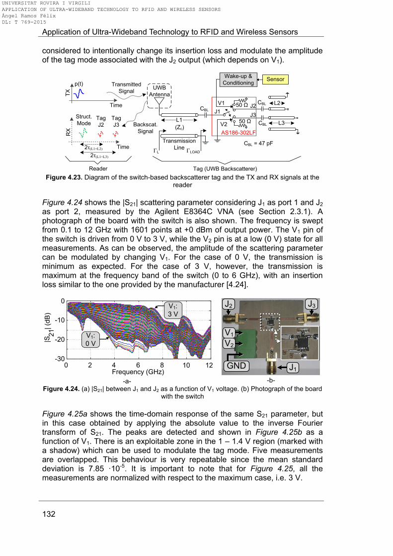
Application of Ultra-Wideband Technology to RFID and Wireless Sensors
132
considered to intentionally change its insertion loss and modulate the amplitude of the tag mode associated with the J2 output (which depends on V1).
UWB
Antenna
L
(Zc)
LOAD
L1
Transmission
LineTime
Struct.
ModeTag
J2
Time
p(t)
2τ(L1+L2)
TX
RX
Transmitted
Signal
Backscat.
Signal
Reader Tag (UWB Backscatterer)
CBL
L2
L3
J2J1
50 ΩV2
AS186-302LF
50 ΩV1
J3
Wake-up &
ConditioningSensor
CBL
CBL
CBL = 47 pF
Tag
J3
2τ(L1+L3)
Figure 4.23. Diagram of the switch-based backscatterer tag and the TX and RX signals at the
reader
Figure 4.24 shows the |S21| scattering parameter considering J1 as port 1 and J2 as port 2, measured by the Agilent E8364C VNA (see Section 2.3.1). A photograph of the board with the switch is also shown. The frequency is swept from 0.1 to 12 GHz with 1601 points at +0 dBm of output power. The V1 pin of the switch is driven from 0 V to 3 V, while the V2 pin is at a low (0 V) state for all measurements. As can be observed, the amplitude of the scattering parameter can be modulated by changing V1. For the case of 0 V, the transmission is minimum as expected. For the case of 3 V, however, the transmission is maximum at the frequency band of the switch (0 to 6 GHz), with an insertion loss similar to the one provided by the manufacturer [4.24].
0 2 4 6 8 10 12-30
-20
-10
0
Frequency (GHz)
|S21| (d
B)
V1:
0 V
V1:
3 V
-a-
J1
J2
V1
V2
GND
J3
-b-
Figure 4.24. (a) |S21| between J1 and J2 as a function of V1 voltage. (b) Photograph of the board with the switch
Figure 4.25a shows the time-domain response of the same S21 parameter, but in this case obtained by applying the absolute value to the inverse Fourier transform of S21. The peaks are detected and shown in Figure 4.25b as a function of V1. There is an exploitable zone in the 1 – 1.4 V region (marked with a shadow) which can be used to modulate the tag mode. Five measurements are overlapped. This behaviour is very repeatable since the mean standard deviation is 7.85 ·10-5. It is important to note that for Figure 4.25, all the measurements are normalized with respect to the maximum case, i.e. 3 V.
UNIVERSITAT ROVIRA I VIRGILI APPLICATION OF ULTRA-WIDEBAND TECHNOLOGY TO RFID AND WIRELESS SENSORS Ángel Ramos Félix DL: T 769-2015
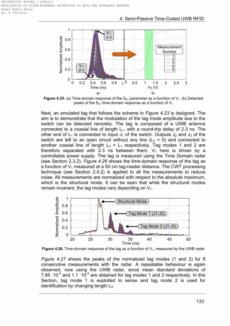
4. Semi-Passive Time-Coded UWB RFID
133
0 0.2 1
0
0.2
0.4
0.6
0.8
1
Time (ns)
No
rma
lize
d A
mp
litu
de
V1:
3 V
V1:
0 V
0 0.5 1 1.5 2 2.5 3V1 (V)
0.4 0.6 0.8
12345
Measurement
Number
-a- -b- Figure 4.25. (a) Time-domain response of the S21 parameter as a function of V1. (b) Detected
peaks of the S21 time-domain response as a function of V1
Next, an emulated tag that follows the scheme in Figure 4.23 is designed. The aim is to demonstrate that the modulation of the tag mode amplitude due to the switch can be detected remotely. The tag is composed of a UWB antenna connected to a coaxial line of length L1, with a round-trip delay of 2.3 ns. The other end of L1 is connected to input J1 of the switch. Outputs J2 and J3 of the switch are left to an open circuit without any line (L2 = 0) and connected to another coaxial line of length L3 = L1 respectively. Tag modes 1 and 2 are therefore separated with 2.3 ns between them. V1 here is driven by a controllable power supply. The tag is measured using the Time Domain radar (see Section 2.3.2). Figure 4.26 shows the time-domain response of the tag as a function of V1 measured at a 50 cm tag-reader distance. The CWT processing technique (see Section 2.4.2) is applied to all the measurements to reduce noise. All measurements are normalized with respect to the absolute maximum, which is the structural mode. It can be seen that while the structural modes remain invariant, the tag modes vary depending on V1.
20 25 30 35 40 45 500
0.2
0.4
0.6
0.8
1
Time (ns)
No
rma
lize
d A
mp
litu
de
Structural Mode
Tag Mode 1 (J1-J2)
Tag Mode 2 (J1-J3)
Figure 4.26. Time-domain response of the tag as a function of V1, measured by the UWB radar
Figure 4.27 shows the peaks of the normalized tag modes (1 and 2) for 8 consecutive measurements with the radar. A repeatable behaviour is again observed, now using the UWB radar, since mean standard deviations of 7.85 ·10-4 and 1.1 ·10-3 are obtained for tag modes 1 and 2 respectively. In this Section, tag mode 1 is exploited to sense and tag mode 2 is used for identification by changing length L3.
UNIVERSITAT ROVIRA I VIRGILI APPLICATION OF ULTRA-WIDEBAND TECHNOLOGY TO RFID AND WIRELESS SENSORS Ángel Ramos Félix DL: T 769-2015
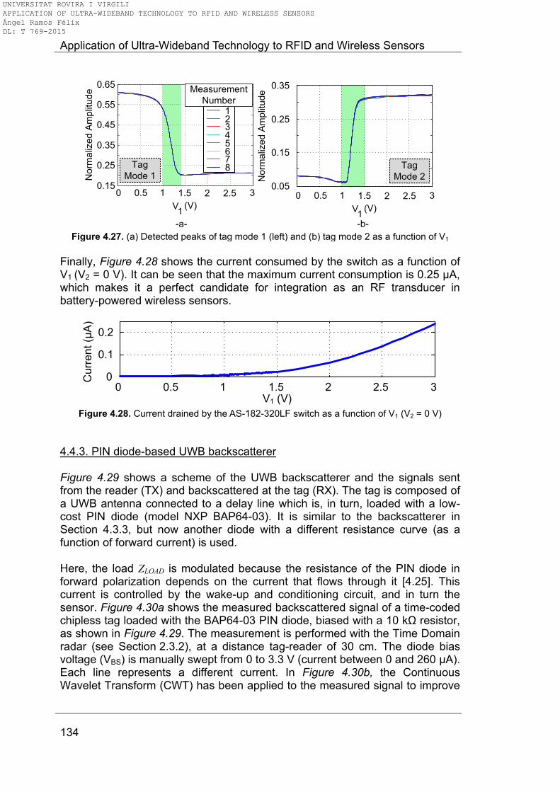
Application of Ultra-Wideband Technology to RFID and Wireless Sensors
134
V1
(V)
0.05
0.15
0.25
0.35
No
rma
lize
d A
mp
litu
de
0 0.5 1 1.5 2 2.5 30.15
0.25
0.35
0.45
0.55
0.65N
orm
aliz
ed
Am
plit
ud
e
12345678
Measurement
Number
V1
(V)
0 0.5 1 1.5 2 2.5 3
Tag
Mode 1Tag
Mode 2
-a- -b- Figure 4.27. (a) Detected peaks of tag mode 1 (left) and (b) tag mode 2 as a function of V1
Finally, Figure 4.28 shows the current consumed by the switch as a function of V1 (V2 = 0 V). It can be seen that the maximum current consumption is 0.25 μA, which makes it a perfect candidate for integration as an RF transducer in battery-powered wireless sensors.
0 0.5 1 1.5 2 2.5 30
0.1
0.2
V1 (V)
Cu
rre
nt (μ
A)
Figure 4.28. Current drained by the AS-182-320LF switch as a function of V1 (V2 = 0 V)
4.4.3. PIN diode-based UWB backscatterer Figure 4.29 shows a scheme of the UWB backscatterer and the signals sent from the reader (TX) and backscattered at the tag (RX). The tag is composed of a UWB antenna connected to a delay line which is, in turn, loaded with a low-cost PIN diode (model NXP BAP64-03). It is similar to the backscatterer in Section 4.3.3, but now another diode with a different resistance curve (as a function of forward current) is used. Here, the load ZLOAD is modulated because the resistance of the PIN diode in forward polarization depends on the current that flows through it [4.25]. This current is controlled by the wake-up and conditioning circuit, and in turn the sensor. Figure 4.30a shows the measured backscattered signal of a time-coded chipless tag loaded with the BAP64-03 PIN diode, biased with a 10 kΩ resistor, as shown in Figure 4.29. The measurement is performed with the Time Domain radar (see Section 2.3.2), at a distance tag-reader of 30 cm. The diode bias voltage (VBS) is manually swept from 0 to 3.3 V (current between 0 and 260 µA). Each line represents a different current. In Figure 4.30b, the Continuous Wavelet Transform (CWT) has been applied to the measured signal to improve
UNIVERSITAT ROVIRA I VIRGILI APPLICATION OF ULTRA-WIDEBAND TECHNOLOGY TO RFID AND WIRELESS SENSORS Ángel Ramos Félix DL: T 769-2015
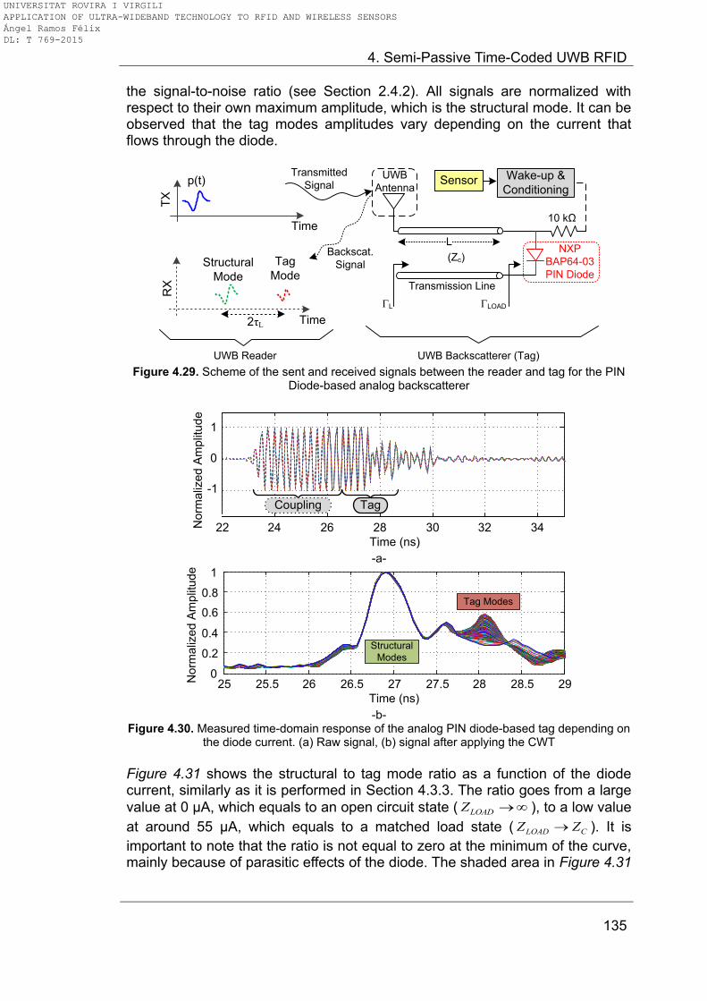
4. Semi-Passive Time-Coded UWB RFID
135
the signal-to-noise ratio (see Section 2.4.2). All signals are normalized with respect to their own maximum amplitude, which is the structural mode. It can be observed that the tag modes amplitudes vary depending on the current that flows through the diode.
10 kΩ
NXP
BAP64-03
PIN Diode
UWB
Antenna
L
(Zc)
LOAD
L
Transmission Line
Time
Structural
Mode
Tag
Mode
Time
p(t)
2τL
TX
RX
Transmitted
Signal
Backscat.
Signal
UWB Reader UWB Backscatterer (Tag)
Wake-up &
ConditioningSensor
Figure 4.29. Scheme of the sent and received signals between the reader and tag for the PIN
Diode-based analog backscatterer
22 24 26 28 30 32 34
-1
0
1
Time (ns)
No
rma
lize
d A
mp
litu
de
Coupling Tag
-a-
0
0.2
0.4
0.6
0.8
1
Norm
aliz
ed
Am
plit
ud
e
25 25.5 26 26.5 27 27.5 28 28.5 29
Time (ns)
Structural
Modes
Tag Modes
-b-
Figure 4.30. Measured time-domain response of the analog PIN diode-based tag depending on the diode current. (a) Raw signal, (b) signal after applying the CWT
Figure 4.31 shows the structural to tag mode ratio as a function of the diode current, similarly as it is performed in Section 4.3.3. The ratio goes from a large
value at 0 μA, which equals to an open circuit state ( LOADZ ), to a low value
at around 55 μA, which equals to a matched load state ( LOAD CZ Z ). It is
important to note that the ratio is not equal to zero at the minimum of the curve, mainly because of parasitic effects of the diode. The shaded area in Figure 4.31
UNIVERSITAT ROVIRA I VIRGILI APPLICATION OF ULTRA-WIDEBAND TECHNOLOGY TO RFID AND WIRELESS SENSORS Ángel Ramos Félix DL: T 769-2015
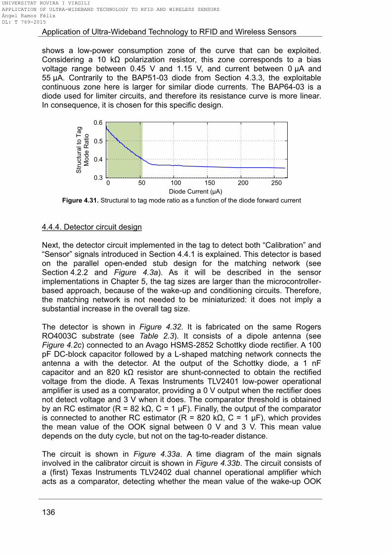
Application of Ultra-Wideband Technology to RFID and Wireless Sensors
136
shows a low-power consumption zone of the curve that can be exploited. Considering a 10 kΩ polarization resistor, this zone corresponds to a bias voltage range between 0.45 V and 1.15 V, and current between 0 μA and 55 μA. Contrarily to the BAP51-03 diode from Section 4.3.3, the exploitable continuous zone here is larger for similar diode currents. The BAP64-03 is a diode used for limiter circuits, and therefore its resistance curve is more linear. In consequence, it is chosen for this specific design.
Diode Current (μA)
0 50 100 150 200 2500.3
0.4
0.5
Str
uctu
ral to
Ta
g
Mo
de
Ra
tio
0.6
Figure 4.31. Structural to tag mode ratio as a function of the diode forward current
4.4.4. Detector circuit design Next, the detector circuit implemented in the tag to detect both “Calibration” and “Sensor” signals introduced in Section 4.4.1 is explained. This detector is based on the parallel open-ended stub design for the matching network (see Section 4.2.2 and Figure 4.3a). As it will be described in the sensor implementations in Chapter 5, the tag sizes are larger than the microcontroller-based approach, because of the wake-up and conditioning circuits. Therefore, the matching network is not needed to be miniaturized: it does not imply a substantial increase in the overall tag size. The detector is shown in Figure 4.32. It is fabricated on the same Rogers RO4003C substrate (see Table 2.3). It consists of a dipole antenna (see Figure 4.2c) connected to an Avago HSMS-2852 Schottky diode rectifier. A 100 pF DC-block capacitor followed by a L-shaped matching network connects the antenna a with the detector. At the output of the Schottky diode, a 1 nF capacitor and an 820 kΩ resistor are shunt-connected to obtain the rectified voltage from the diode. A Texas Instruments TLV2401 low-power operational amplifier is used as a comparator, providing a 0 V output when the rectifier does not detect voltage and 3 V when it does. The comparator threshold is obtained by an RC estimator (R = 82 kΩ, C = 1 μF). Finally, the output of the comparator is connected to another RC estimator (R = 820 kΩ, C = 1 μF), which provides the mean value of the OOK signal between 0 V and 3 V. This mean value depends on the duty cycle, but not on the tag-to-reader distance.
The circuit is shown in Figure 4.33a. A time diagram of the main signals involved in the calibrator circuit is shown in Figure 4.33b. The circuit consists of a (first) Texas Instruments TLV2402 dual channel operational amplifier which acts as a comparator, detecting whether the mean value of the wake-up OOK
UNIVERSITAT ROVIRA I VIRGILI APPLICATION OF ULTRA-WIDEBAND TECHNOLOGY TO RFID AND WIRELESS SENSORS Ángel Ramos Félix DL: T 769-2015
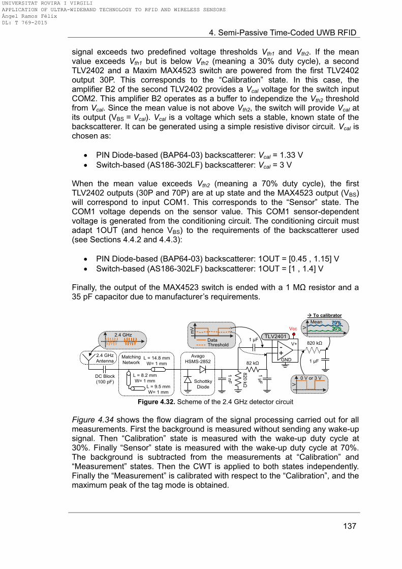
4. Semi-Passive Time-Coded UWB RFID
137
signal exceeds two predefined voltage thresholds Vth1 and Vth2. If the mean value exceeds Vth1 but is below Vth2 (meaning a 30% duty cycle), a second TLV2402 and a Maxim MAX4523 switch are powered from the first TLV2402 output 30P. This corresponds to the “Calibration” state. In this case, the amplifier B2 of the second TLV2402 provides a Vcal voltage for the switch input COM2. This amplifier B2 operates as a buffer to independize the Vth2 threshold from Vcal. Since the mean value is not above Vth2, the switch will provide Vcal at its output (VBS = Vcal). Vcal is a voltage which sets a stable, known state of the backscatterer. It can be generated using a simple resistive divisor circuit. Vcal is chosen as:
PIN Diode-based (BAP64-03) backscatterer: Vcal = 1.33 V
Switch-based (AS186-302LF) backscatterer: Vcal = 3 V When the mean value exceeds Vth2 (meaning a 70% duty cycle), the first TLV2402 outputs (30P and 70P) are at up state and the MAX4523 output (VBS) will correspond to input COM1. This corresponds to the “Sensor” state. The COM1 voltage depends on the sensor value. This COM1 sensor-dependent voltage is generated from the conditioning circuit. The conditioning circuit must adapt 1OUT (and hence VBS) to the requirements of the backscatterer used (see Sections 4.4.2 and 4.4.3):
PIN Diode-based (BAP64-03) backscatterer: 1OUT = [0.45 , 1.15] V
Switch-based (AS186-302LF) backscatterer: 1OUT = [1 , 1.4] V
Finally, the output of the MAX4523 switch is ended with a 1 MΩ resistor and a 35 pF capacitor due to manufacturer‟s requirements.
DC Block
(100 pF)
L = 14.8 mm
W= 1 mm
Avago
HSMS-2852
1 n
F
820
kΩSchottky
Diode
2.4 GHz
2.4 GHz
Antenna
820 kΩ
1 µF
L = 8.2 mm
W= 1 mm
L = 9.5 mm
W= 1 mm
+-
Matching
Network
à To calibrator
30%30%70%70%Mean
82 kΩ
1 µ
F
1 µF
mV V
DataThreshold
V
0 V or 3 V
TLV2401
Vcc
V+
GND
Figure 4.32. Scheme of the 2.4 GHz detector circuit
Figure 4.34 shows the flow diagram of the signal processing carried out for all measurements. First the background is measured without sending any wake-up signal. Then “Calibration” state is measured with the wake-up duty cycle at 30%. Finally “Sensor” state is measured with the wake-up duty cycle at 70%. The background is subtracted from the measurements at “Calibration” and “Measurement” states. Then the CWT is applied to both states independently. Finally the “Measurement” is calibrated with respect to the “Calibration”, and the maximum peak of the tag mode is obtained.
UNIVERSITAT ROVIRA I VIRGILI APPLICATION OF ULTRA-WIDEBAND TECHNOLOGY TO RFID AND WIRELESS SENSORS Ángel Ramos Félix DL: T 769-2015

Application of Ultra-Wideband Technology to RFID and Wireless Sensors
138
Sensor
Vcc
Vth1
Vth2
Mean
30%30%70%70%
NO1
V+
COM1
IN1
NC2COM2
IN2
1 M
Ω
35 p
F
+-
+-
V+
GNDTLV2402
Vcal
MAX4523
V-, GND
A1
A2
+-
+-
V+
GND
TLV2402
B1
B2
à To UWB
Backscatterer
1O
UT
2O
UT
30
P
VBS
70P
Conditoning
Circuit
Vcal
-a-
VBS0 V
Vcal V
3 V
1. UWB Clutter
0 V30P
3 V
0 V
Vcal V0 V
Vcal V0 V
2. Reader sends 30%
3. UWB Cal.
70P
1OUT
2OUT
5. UWB Sensor
Reader OFF
SensorCalibration
4. Reader sends 70%
-b-
Figure 4.33. (a) Scheme of the calibrator circuit. (b) Time diagram of the signals
BackgroundVBS = 0 V
Wake-up Off (0%)
CalibrationVBS = VCal
Wake-up at 30%
MeasurementVBS = 1OUT
Wake-up at 70%
--
Calibrated
Tag ModeRatio ∕
CWT CWT
Peak
Figure 4.34. Flow diagram of the signal processing with the analog semi-passive UWB RFID
system
4.5. Discussion, comparison between systems and conclusions This chapter has presented two sensing platforms for remote identification and sensing based on time-coded UWB RFID:
A digital approach, based on a commercial microcontroller
An analog approach, based on operational amplifiers, DC switches and passive elements
UNIVERSITAT ROVIRA I VIRGILI APPLICATION OF ULTRA-WIDEBAND TECHNOLOGY TO RFID AND WIRELESS SENSORS Ángel Ramos Félix DL: T 769-2015
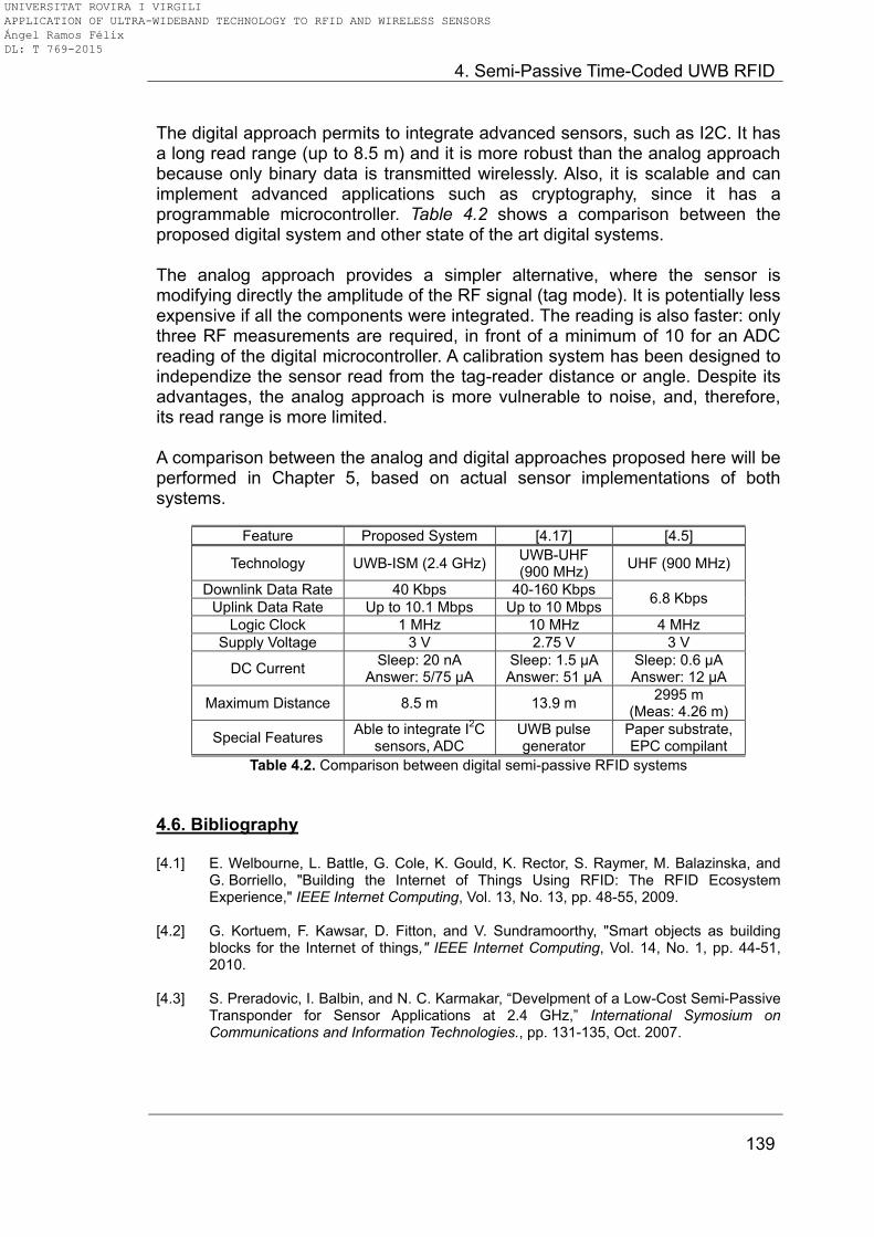
4. Semi-Passive Time-Coded UWB RFID
139
The digital approach permits to integrate advanced sensors, such as I2C. It has a long read range (up to 8.5 m) and it is more robust than the analog approach because only binary data is transmitted wirelessly. Also, it is scalable and can implement advanced applications such as cryptography, since it has a programmable microcontroller. Table 4.2 shows a comparison between the proposed digital system and other state of the art digital systems. The analog approach provides a simpler alternative, where the sensor is modifying directly the amplitude of the RF signal (tag mode). It is potentially less expensive if all the components were integrated. The reading is also faster: only three RF measurements are required, in front of a minimum of 10 for an ADC reading of the digital microcontroller. A calibration system has been designed to independize the sensor read from the tag-reader distance or angle. Despite its advantages, the analog approach is more vulnerable to noise, and, therefore, its read range is more limited. A comparison between the analog and digital approaches proposed here will be performed in Chapter 5, based on actual sensor implementations of both systems.
Feature Proposed System [4.17] [4.5]
Technology UWB-ISM (2.4 GHz) UWB-UHF (900 MHz)
UHF (900 MHz)
Downlink Data Rate 40 Kbps 40-160 Kbps 6.8 Kbps
Uplink Data Rate Up to 10.1 Mbps Up to 10 Mbps
Logic Clock 1 MHz 10 MHz 4 MHz
Supply Voltage 3 V 2.75 V 3 V
DC Current Sleep: 20 nA
Answer: 5/75 μA Sleep: 1.5 μA Answer: 51 μA
Sleep: 0.6 μA Answer: 12 μA
Maximum Distance 8.5 m 13.9 m 2995 m
(Meas: 4.26 m)
Special Features Able to integrate I
2C
sensors, ADC UWB pulse generator
Paper substrate, EPC compilant
Table 4.2. Comparison between digital semi-passive RFID systems
4.6. Bibliography [4.1] E. Welbourne, L. Battle, G. Cole, K. Gould, K. Rector, S. Raymer, M. Balazinska, and
G. Borriello, "Building the Internet of Things Using RFID: The RFID Ecosystem Experience," IEEE Internet Computing, Vol. 13, No. 13, pp. 48-55, 2009.
[4.2] G. Kortuem, F. Kawsar, D. Fitton, and V. Sundramoorthy, "Smart objects as building
blocks for the Internet of things," IEEE Internet Computing, Vol. 14, No. 1, pp. 44-51, 2010.
[4.3] S. Preradovic, I. Balbin, and N. C. Karmakar, “Develpment of a Low-Cost Semi-Passive
Transponder for Sensor Applications at 2.4 GHz,” International Symosium on Communications and Information Technologies., pp. 131-135, Oct. 2007.
UNIVERSITAT ROVIRA I VIRGILI APPLICATION OF ULTRA-WIDEBAND TECHNOLOGY TO RFID AND WIRELESS SENSORS Ángel Ramos Félix DL: T 769-2015
Application of Ultra-Wideband Technology to RFID and Wireless Sensors
140
[4.4] J. Yin, J. Yi, M. K. Law, Y. Ling, M. C. Lee, K. P. Ng, B. Gao, H. C. Luong, A. Bermak, M. Chan, W-H. Ki, C-Y. Tsui, and M. Yuen, "A System-on-Chip EPC Gen-2 Passive UHF RFID Tag With Embedded Temperature Sensor," IEEE Journal of Solid-State Circuits, Vol. 45, No. 11, pp. 2404-2420, Nov. 2010.
[4.5] R. Vykas, V. Lakafosis, A. Rida, N. Chaisilwattana, S. Travis, J. Pan, and
M. M. Tentzeris, “Paper-Based RFID-Enabled Wireless Platforms for Sensing Applications,” IEEE Transactions on Microwave Theory and Techniques, Vol. 57, No. 5, pp. 1370-1382, 2009.
[4.6] M. Loy, R. Karingattil, and L. Williams - Texas Instruments, "Application Report - SWRA048 - ISM-Band and Short Range Device Regulatory Compliance Overview," http://www.ti.com/lit/an/swra048/swra048.pdf, Nov. 2014 [Nov. 1, 2014]
[4.7] A. M. Cowley and H. O. Sorensen, “Quantitative Comparison of Solid-State Microwave Detectors,” IEEE Transactions on Microwave Theory and Techniques, Vol. 14, No. 12, pp. 588-602, 1966.
[4.8] S. Hemour and K. Wu, “Radio-Frequency Rectifier for Electromagnetic Energy Harvesting: Development Path and Future Outlook,” Proceedings of the IEEE, Vol. 102, No. 11, pp. 1667-1691, 2014.
[4.9] H. Jabbar, Y. S. Song, and T. T. Jeong, “RF energy harvesting system and circuits for charging of mobile devices,” IEEE Transactions on Consumer Electronics, Vol. 56, No. 1, pp. 247-253, 2010.
[4.10] A. Georgiadis, G. Andia Vera, and A. Collado, “Rectenna design and optimization using reciprocity theory and harmonic balance analysis for electromagnetic (EM) energy harvesting,” IEEE Antennas and Wireless Propagation Letters, Vol. 9, pp. 444-446, 2010.
[4.11] R. D. Fernandes, A. S. Boaventura, N. B. Carvalho, and J. N. Matos, “Increasing the Range of Wireless Passive Sensor Nodes using Multisines,” 2011 IEEE International Conference on RFID-Technologies and Applications (RFID-TA), pp. 549-553, 2011.
[4.12] Avago Technologies, “HSMS-285x Series Surface Mount Zero Bias Schottky Detector Diodes,” http://www.avagotech.com/docs/AV02-1377EN, Nov. 2014 [Nov. 1, 2014].
[4.13] Hewlett-Packard, "All Schottky Diodes are Zero Bias Detectors," Application Note 988, 1982.
[4.14] Microchip Technology Inc., “PIC 16(L)F1827 8-bit Flash MCU with Nanowatt XLP,” http://www.microchip.com/wwwproducts/Devices.aspx?dDocName=en538963, Nov. 2014 [Nov. 1, 2014].
[4.15] Texas Instruments, "MSP430FR59XX Mixed-Signal Microcontrollers," SLAS704D, Oct. 2012.
[4.16] Atmel, "8-bit AVR Microcontroller with 4K Bytes In-System Programmable Flash and Boost Converter," ATtiny43U, 2012.
[4.17] M. Baghaei-Nejad, D. S. Mendoza, Z. Zou, S. Radiom, G. Gielen, L-R. Zheng, and H. Tenhunen, “A Remote-Powered RFID Tag with 10Mb/s UWB Uplink and -18.5dBm Sensitivity UHF Downlink in 0.18 μm CMOS,” Digest of Technical Papers, ISSCC2009, 2009.
[4.18] NXP Semiconductors, “BAP51-03 General purpose PIN diode,” http://www.nxp.com/documents/data_sheet/BAP51-03.pdf, Feb. 11, 2004 [Mar. 27,
UNIVERSITAT ROVIRA I VIRGILI APPLICATION OF ULTRA-WIDEBAND TECHNOLOGY TO RFID AND WIRELESS SENSORS Ángel Ramos Félix DL: T 769-2015
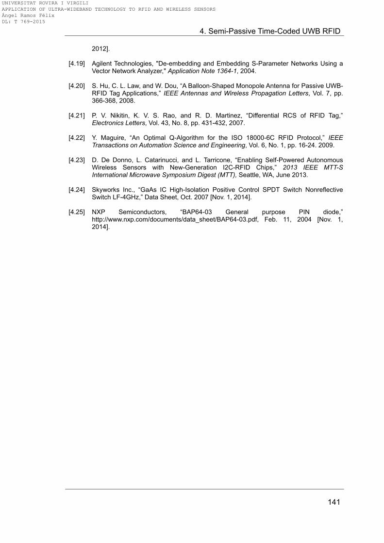
4. Semi-Passive Time-Coded UWB RFID
141
2012].
[4.19] Agilent Technologies, "De-embedding and Embedding S-Parameter Networks Using a Vector Network Analyzer," Application Note 1364-1, 2004.
[4.20] S. Hu, C. L. Law, and W. Dou, “A Balloon-Shaped Monopole Antenna for Passive UWB-RFID Tag Applications,” IEEE Antennas and Wireless Propagation Letters, Vol. 7, pp. 366-368, 2008.
[4.21] P. V. Nikitin, K. V. S. Rao, and R. D. Martinez, “Differential RCS of RFID Tag,” Electronics Letters, Vol. 43, No. 8, pp. 431-432, 2007.
[4.22] Y. Maguire, “An Optimal Q-Algorithm for the ISO 18000-6C RFID Protocol,” IEEE Transactions on Automation Science and Engineering, Vol. 6, No. 1, pp. 16-24. 2009.
[4.23] D. De Donno, L. Catarinucci, and L. Tarricone, “Enabling Self-Powered Autonomous Wireless Sensors with New-Generation I2C-RFID Chips,” 2013 IEEE MTT-S International Microwave Symposium Digest (MTT), Seattle, WA, June 2013.
[4.24] Skyworks Inc., “GaAs IC High-Isolation Positive Control SPDT Switch Nonreflective Switch LF-4GHz,” Data Sheet, Oct. 2007 [Nov. 1, 2014].
[4.25] NXP Semiconductors, “BAP64-03 General purpose PIN diode,” http://www.nxp.com/documents/data_sheet/BAP64-03.pdf, Feb. 11, 2004 [Nov. 1, 2014].
UNIVERSITAT ROVIRA I VIRGILI APPLICATION OF ULTRA-WIDEBAND TECHNOLOGY TO RFID AND WIRELESS SENSORS Ángel Ramos Félix DL: T 769-2015

Application of Ultra-Wideband Technology to RFID and Wireless Sensors
142
UNIVERSITAT ROVIRA I VIRGILI APPLICATION OF ULTRA-WIDEBAND TECHNOLOGY TO RFID AND WIRELESS SENSORS Ángel Ramos Félix DL: T 769-2015
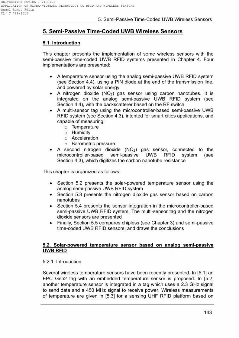
5. Semi-Passive Time-Coded UWB Wireless Sensors
143
5. Semi-Passive Time-Coded UWB Wireless Sensors 5.1. Introduction This chapter presents the implementation of some wireless sensors with the semi-passive time-coded UWB RFID systems presented in Chapter 4. Four implementations are presented:
A temperature sensor using the analog semi-passive UWB RFID system (see Section 4.4), using a PIN diode at the end of the transmission line, and powered by solar energy
A nitrogen dioxide (NO2) gas sensor using carbon nanotubes. It is integrated on the analog semi-passive UWB RFID system (see Section 4.4), with the backscatterer based on the RF switch
A multi-sensor tag using the microcontroller-based semi-passive UWB RFID system (see Section 4.3), intented for smart cities applications, and capable of measuring:
o Temperature o Humidity o Acceleration o Barometric pressure
A second nitrogen dioxide (NO2) gas sensor, connected to the microcontroller-based semi-passive UWB RFID system (see Section 4.3), which digitizes the carbon nanotube resistance
This chapter is organized as follows:
Section 5.2 presents the solar-powered temperature sensor using the analog semi-passive UWB RFID system
Section 5.3 presents the nitrogen dioxide gas sensor based on carbon nanotubes
Section 5.4 presents the sensor integration in the microcontroller-based semi-passive UWB RFID system. The multi-sensor tag and the nitrogen dioxide sensors are presented
Finally, Section 5.5 compares chipless (see Chapter 3) and semi-passive time-coded UWB RFID sensors, and draws the conclusions
5.2. Solar-powered temperature sensor based on analog semi-passive UWB RFID 5.2.1. Introduction Several wireless temperature sensors have been recently presented. In [5.1] an
EPC Gen2 tag with an embedded temperature sensor is proposed. In [5.2]
another temperature sensor is integrated in a tag which uses a 2.3 GHz signal
to send data and a 450 MHz signal to receive power. Wireless measurements
of temperature are given in [5.3] for a sensing UHF RFID platform based on
UNIVERSITAT ROVIRA I VIRGILI APPLICATION OF ULTRA-WIDEBAND TECHNOLOGY TO RFID AND WIRELESS SENSORS Ángel Ramos Félix DL: T 769-2015
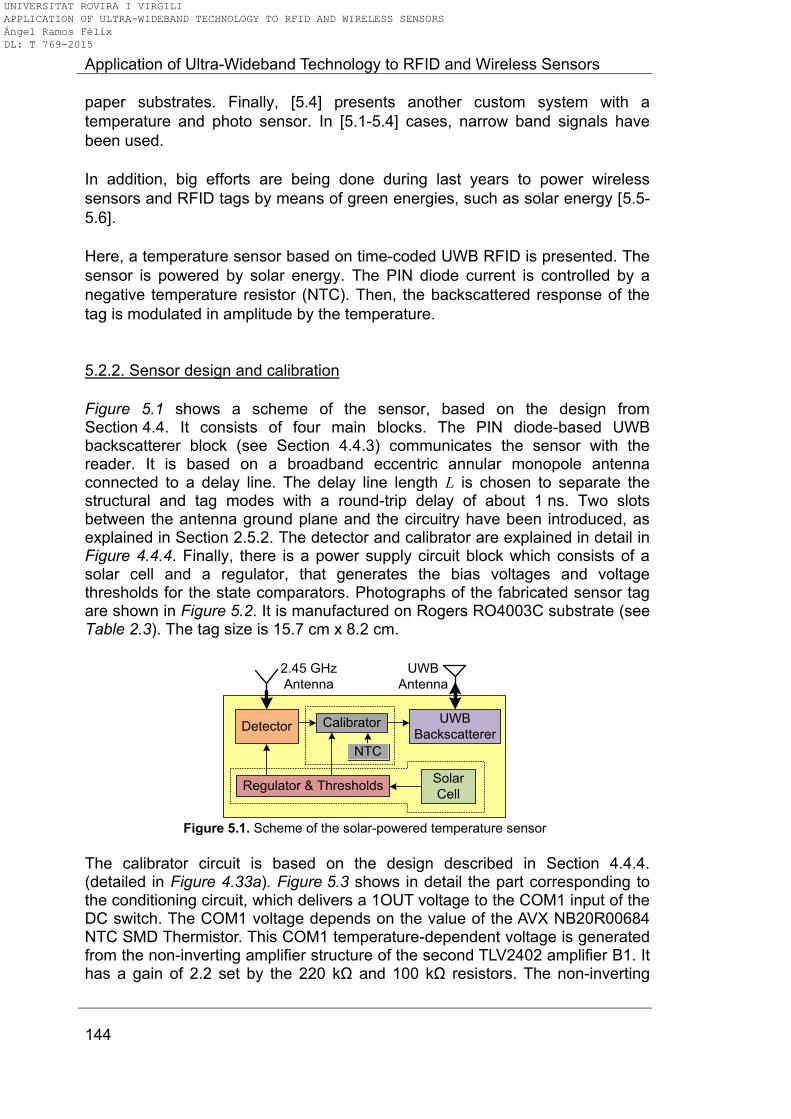
Application of Ultra-Wideband Technology to RFID and Wireless Sensors
144
paper substrates. Finally, [5.4] presents another custom system with a
temperature and photo sensor. In [5.1-5.4] cases, narrow band signals have
been used.
In addition, big efforts are being done during last years to power wireless
sensors and RFID tags by means of green energies, such as solar energy [5.5-
5.6].
Here, a temperature sensor based on time-coded UWB RFID is presented. The
sensor is powered by solar energy. The PIN diode current is controlled by a
negative temperature resistor (NTC). Then, the backscattered response of the
tag is modulated in amplitude by the temperature.
5.2.2. Sensor design and calibration
Figure 5.1 shows a scheme of the sensor, based on the design from Section 4.4. It consists of four main blocks. The PIN diode-based UWB backscatterer block (see Section 4.4.3) communicates the sensor with the reader. It is based on a broadband eccentric annular monopole antenna connected to a delay line. The delay line length L is chosen to separate the structural and tag modes with a round-trip delay of about 1 ns. Two slots between the antenna ground plane and the circuitry have been introduced, as explained in Section 2.5.2. The detector and calibrator are explained in detail in Figure 4.4.4. Finally, there is a power supply circuit block which consists of a solar cell and a regulator, that generates the bias voltages and voltage thresholds for the state comparators. Photographs of the fabricated sensor tag are shown in Figure 5.2. It is manufactured on Rogers RO4003C substrate (see Table 2.3). The tag size is 15.7 cm x 8.2 cm.
Detector Calibrator
Regulator & Thresholds
UWB
Backscatterer
2.45 GHz
Antenna
UWB
Antenna
NTC
Solar
Cell
Figure 5.1. Scheme of the solar-powered temperature sensor
The calibrator circuit is based on the design described in Section 4.4.4. (detailed in Figure 4.33a). Figure 5.3 shows in detail the part corresponding to the conditioning circuit, which delivers a 1OUT voltage to the COM1 input of the DC switch. The COM1 voltage depends on the value of the AVX NB20R00684 NTC SMD Thermistor. This COM1 temperature-dependent voltage is generated from the non-inverting amplifier structure of the second TLV2402 amplifier B1. It has a gain of 2.2 set by the 220 kΩ and 100 kΩ resistors. The non-inverting
UNIVERSITAT ROVIRA I VIRGILI APPLICATION OF ULTRA-WIDEBAND TECHNOLOGY TO RFID AND WIRELESS SENSORS Ángel Ramos Félix DL: T 769-2015
5. Semi-Passive Time-Coded UWB Wireless Sensors
145
input IN1+ is the voltage at the NTC in parallel with a 150 kΩ resistor, minus the voltage drop at the 820 kΩ series resistor. With these values, the output voltage 1OUT is between 0.6 V at 70 ºC (NTC = 420 kΩ) and 1.2 V at 35 ºC (NTC = 98 kΩ). It corresponds to the shaded zone of the PIN-diode backscatterer (see Section 4.4.3).
NTCCalibratorCalibrator
UWB
Backscatterer
UWB
Backscatterer
Regulator &
Threhsolds
Regulator &
Threhsolds
2.45 GHz
Detector
2.45 GHz
Detector
-a-
UWB BackscattererUWB Backscatterer
2.45 GHz
Antenna
2.45 GHz
Antenna
Solar
Cell
Solar
Cell
-b-
Figure 5.2. Fabricated solar-powered temperature sensor, (a) top face and (b) bottom face
1.33 V (~ 32 ºC)
NTC
(680 kΩ)150 kΩ
820 kΩ
100 kΩ 220 kΩ
Vcal
+-
+-
V+
GND
TLV2402
B1
B2
1O
UT
2O
UT
30
P (
3 V
)
Conditioning Circuit
Temp.
V
To COM1
Figure 5.3. Scheme of the signal conditioning circuit for the temperature sensor
UNIVERSITAT ROVIRA I VIRGILI APPLICATION OF ULTRA-WIDEBAND TECHNOLOGY TO RFID AND WIRELESS SENSORS Ángel Ramos Félix DL: T 769-2015

Application of Ultra-Wideband Technology to RFID and Wireless Sensors
146
5.2.3. Solar-cell integration. Power requirements The flexible amorphous silicon Power Film SP3-37 solar cell is selected. The specifications of SP3-37 are an open circuit voltage Voc = 4.1 V and a short circuit current Isc = 28 mA, when illuminated by a light source complying with the standard AM1.5G global solar irradiance spectrum [5.7], T = 25 ºC and 1 sun (= 100 mW/cm2) irradiance. The SP3-37, shown in Figure 5.4, is rectangular with dimensions 64 mm by 37 mm. In Figure 5.4 one can see the positive and negative terminals of the solar cell as well as a number of conductive strips on its top surface. The cell itself is a small solar module consisting of five smaller cells isolated by each of the four intermediate horizontal conductive strips which are electrically connected in series. Each of the individual cells provides an open circuit voltage Voc = 0.82 V and short circuit current Isc = 28 mA, set by the width of the cell. The integration of solar cells with antennas has been originally proposed in [5.8]. The placement of a solar cell on top of a printed antenna does not affect the antenna performance provided that the area of the conductive surface of the antenna where the current density is high, such as near the feed point and the radiating edges, is not covered by the cell [5.8-5.9]. This fact allows to significantly reduce the total area required for the circuitry and solar cells, allowing for a more compact system implementation. The solar cell used to power the sensor is therefore integrated on the UWB antenna ground plane. In order to avoid placing the solar cell near the antenna feed point and due to the presence of the circular disc aperture in the ground plane limiting the available area, it was necessary to cut the original cell along its length into two pieces capable to produce an open circuit voltage Voc = 4.1 V and a short circuit current Isc = 14 mA under 1 sun irradiance. As it is shown in Figure 5.5, it is necessary to further shape the two pieces in order to conform to the ground plane conductive area leading to a non-uniform width which results in a slightly reduced current capability. The current capability of each solar cell piece alone is sufficient to power the sensor circuitry.
Figure 5.5 shows the measured |S11| parameter of the UWB monopole with and without two solar cells. There are two measurements, one with the solar cells placed with a 1 mm gap between the circular slot and the cell and the other with a 2 mm gap. The antenna performance is not affected at all by the cells. Each cell has sufficient current capability to power the sensor tag. As a result only one cell is placed in the final circuit prototype as it can be observed in Figure 5.2b. It should be noted that the negative terminal of the cell is directly soldered on the ground plane conductor while the positive terminal of the cell is connected to the circuit supply using an insulated wire. The output of the solar cell is connected to a Linear Technologies LT1763 (LT1763CS8#PBF) variable voltage regulator. As shown in Figure 5.6, it is
UNIVERSITAT ROVIRA I VIRGILI APPLICATION OF ULTRA-WIDEBAND TECHNOLOGY TO RFID AND WIRELESS SENSORS Ángel Ramos Félix DL: T 769-2015

5. Semi-Passive Time-Coded UWB Wireless Sensors
147
adjusted to provide a 3 V output with two resistors of 500 kΩ and 750 kΩ,
according to the manufacturer: 2 1 21.22 1 / ADJVcc R R I R , where
IADJ = 30 nA typically. The thresholds needed for the detector and calibrator circuits are obtained using a simple resistive circuit.
Figure 5.4. Power Film SP3-37 solar cell
0 2 4 6 8 10 12
0
-5
-10
-15
-20
-25
Without solar cell
With solar cell (gap = 2 mm)
With solar cell (gap = 1 mm)
|S1
1| (d
B)
Frequency (GHz)
gapgap
Figure 5.5. Measured |S11| parameter of the tag antenna without and with the solar cell
IN
LT1763
GND
ADJSHDN
OUTR2
750 kΩ
R1
500 kΩ
470 kΩ1 MΩ 330 kΩ
Vth1Vth2 Vcal
0.55 V1.333 V
VccSolar Cell
Figure 5.6. Scheme of the solar cell connected to the regulator and the resistive values for the
thresholds
The tag needs to work by its own power source (in this case, solar energy). Since the consumption is a major concern in autonomous sensors, a study is carried out here. Table 5.1 shows the current consumption of each element in the tag circuitry. As expected, the most consuming element is the PIN diode,
UNIVERSITAT ROVIRA I VIRGILI APPLICATION OF ULTRA-WIDEBAND TECHNOLOGY TO RFID AND WIRELESS SENSORS Ángel Ramos Félix DL: T 769-2015
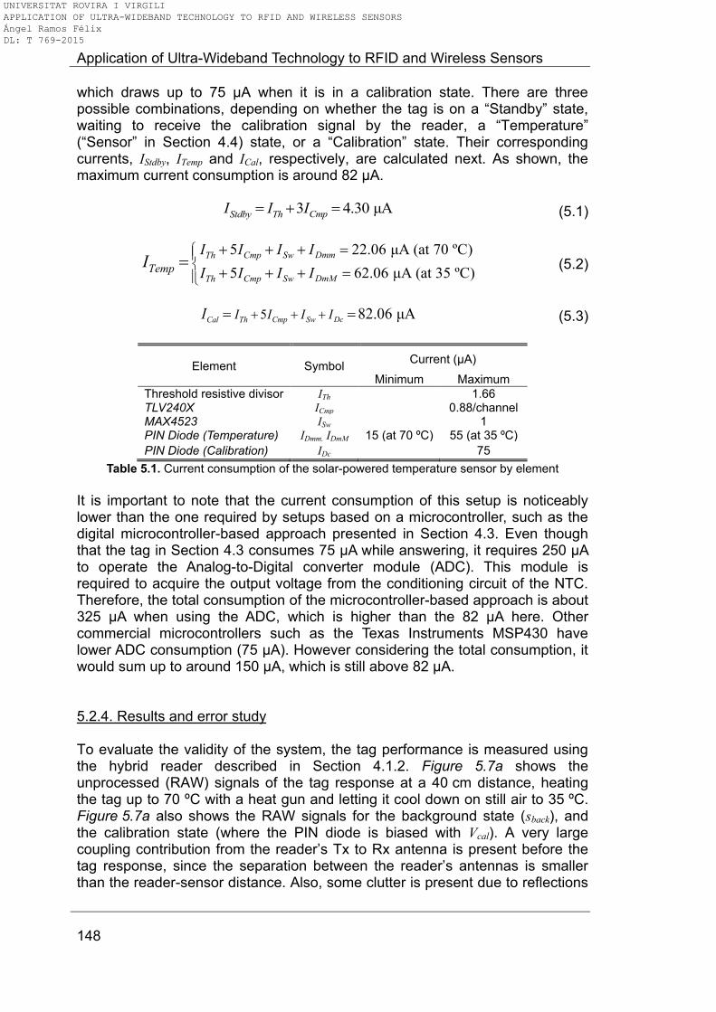
Application of Ultra-Wideband Technology to RFID and Wireless Sensors
148
which draws up to 75 μA when it is in a calibration state. There are three possible combinations, depending on whether the tag is on a “Standby” state, waiting to receive the calibration signal by the reader, a “Temperature” (“Sensor” in Section 4.4) state, or a “Calibration” state. Their corresponding currents, IStdby, ITemp and ICal, respectively, are calculated next. As shown, the maximum current consumption is around 82 μA.
3 4.30 μACmpStdby ThI I I (5.1)
5 22.06 μA (at 70 ºC)
5 62.06 μA (at 35 ºC)
DmmCmp SwTh
DmMCmp SwThTemp
I I I I
I I I II
(5.2)
5 82.06 μADcCmp SwCal ThI I I II (5.3)
Element Symbol Current (μA)
Minimum Maximum
Threshold resistive divisor ITh 1.66 TLV240X ICmp 0.88/channel MAX4523 ISw 1 PIN Diode (Temperature) IDmm, IDmM 15 (at 70 ºC) 55 (at 35 ºC)
PIN Diode (Calibration) IDc 75
Table 5.1. Current consumption of the solar-powered temperature sensor by element
It is important to note that the current consumption of this setup is noticeably lower than the one required by setups based on a microcontroller, such as the digital microcontroller-based approach presented in Section 4.3. Even though that the tag in Section 4.3 consumes 75 μA while answering, it requires 250 μA to operate the Analog-to-Digital converter module (ADC). This module is required to acquire the output voltage from the conditioning circuit of the NTC. Therefore, the total consumption of the microcontroller-based approach is about 325 μA when using the ADC, which is higher than the 82 μA here. Other commercial microcontrollers such as the Texas Instruments MSP430 have lower ADC consumption (75 μA). However considering the total consumption, it would sum up to around 150 μA, which is still above 82 μA. 5.2.4. Results and error study To evaluate the validity of the system, the tag performance is measured using the hybrid reader described in Section 4.1.2. Figure 5.7a shows the unprocessed (RAW) signals of the tag response at a 40 cm distance, heating the tag up to 70 ºC with a heat gun and letting it cool down on still air to 35 ºC. Figure 5.7a also shows the RAW signals for the background state (sback), and the calibration state (where the PIN diode is biased with Vcal). A very large coupling contribution from the reader‟s Tx to Rx antenna is present before the tag response, since the separation between the reader‟s antennas is smaller than the reader-sensor distance. Also, some clutter is present due to reflections
UNIVERSITAT ROVIRA I VIRGILI APPLICATION OF ULTRA-WIDEBAND TECHNOLOGY TO RFID AND WIRELESS SENSORS Ángel Ramos Félix DL: T 769-2015

5. Semi-Passive Time-Coded UWB Wireless Sensors
149
with surrounding objects. Figure 5.7b shows the zoomed area corresponding to the tag response. The structural modes, as shown, remain identical for all the possible temperatures of the tag. On the contrary, the tag modes amplitudes change. The tag mode with the largest amplitude corresponds to the sback state, which corresponds to the tag measurement without any current flowing through the diode, that is without any 2.45 GHz calibration signal sent to the tag. With this background measurement, the clutter and coupling contributions can be diminished without having to measure the empty-room response.
20 25 30 35 40 45 50-1
-0.6
-0.2
0.2
0.6
1
Time (ns)
No
rma
lize
d A
mp
litu
de
Tag
Response
Coupling
Clutter
-a-
-0.4
-0.2
0
0.2
0.4
29 29.5 30 30.5 31 31.5 32Time (ns)
Norm
aliz
ed
Am
plit
ud
e
Structural
Modes Tag Modes
Diode Off
(Background)
-b-
Figure 5.7. (a) Unprocessed time domain signals for the tag response from 35 ºC to 70 ºC. (b) Zoomed tag response
To enhance the tag modes, for each measurement si (which contains the coupling contribution, the structural and tag modes, and clutter) the background sback is subtracted as shown in Figure 5.8. It can be clearly observed that the coupling contribution and clutter have been diminished in front of the tag mode. Since the structural mode is also the same for the background (the tag is always present at the scene), it is also removed. Figure 5.9 shows the background-subtracted signal from Figure 5.7 after applying the CWT. As shown in the inset of Figure 5.9, the amplitude grows when temperature changes from 35 ºC to 70 ºC. All amplitudes are normalized with respect to the calibration state. The calibration to temperature ratio can be defined as the ratio between the amplitude in the calibration state and the amplitude in the temperature measurement state. It can be obtained by detecting the peaks of the tag modes
UNIVERSITAT ROVIRA I VIRGILI APPLICATION OF ULTRA-WIDEBAND TECHNOLOGY TO RFID AND WIRELESS SENSORS Ángel Ramos Félix DL: T 769-2015
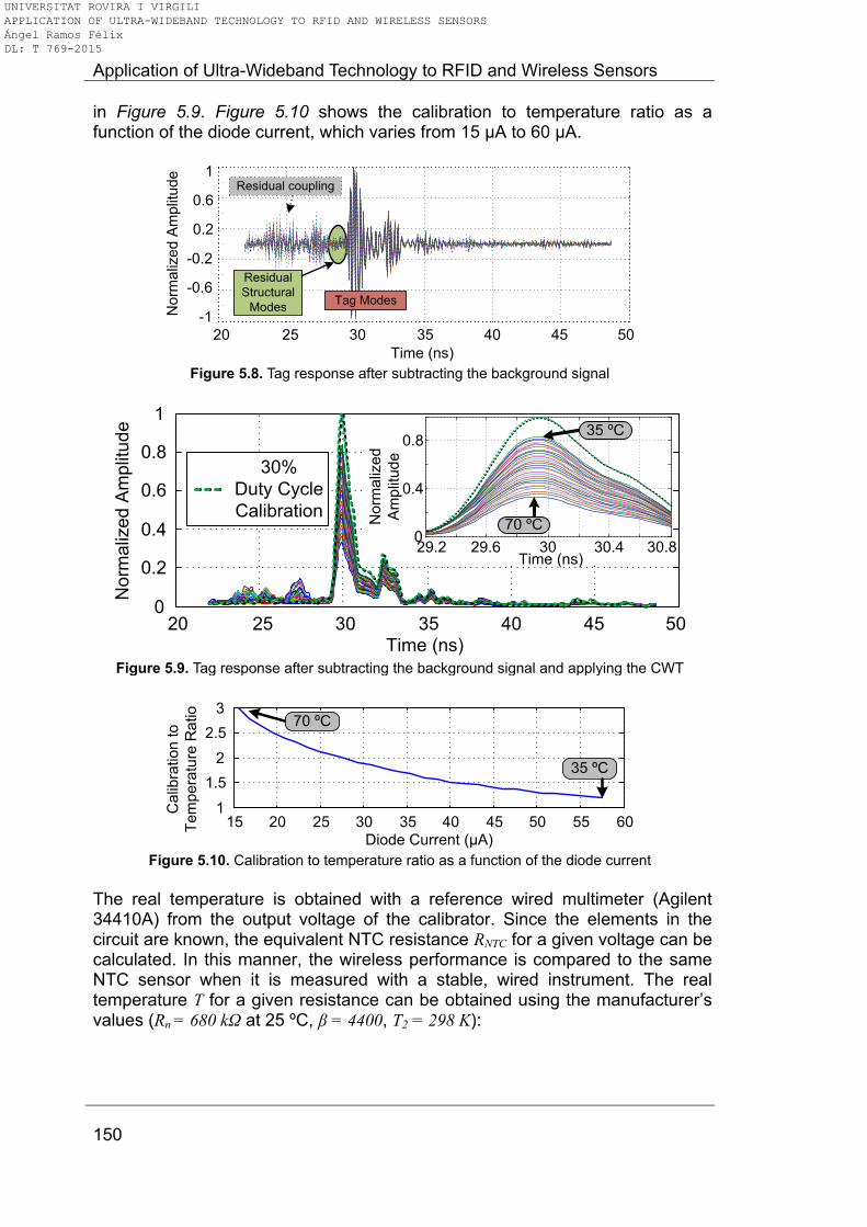
Application of Ultra-Wideband Technology to RFID and Wireless Sensors
150
in Figure 5.9. Figure 5.10 shows the calibration to temperature ratio as a function of the diode current, which varies from 15 μA to 60 μA.
20 25 30 35 40 45 50
-1
-0.6
-0.2
0.2
0.6
1
Time (ns)
No
rma
lize
d A
mp
litu
de
Residual coupling
Tag Modes
Residual
Structural
Modes
Figure 5.8. Tag response after subtracting the background signal
0
0.2
0.4
0.6
0.8
1
20 25 30 35 40 45 50Time (ns)
No
rma
lize
d A
mp
litu
de
29.2 29.6 30 30.4 30.80
0.4
0.8
Time (ns)
No
rma
lize
d
Am
plit
ud
e
30%
Duty Cycle
Calibration
35 ºC
70 ºC
Figure 5.9. Tag response after subtracting the background signal and applying the CWT
15 20 25 30 35 40 45 50 55 601
1.5
2
2.5
3
Diode Current (μA)
Calib
ratio
n to
Tem
pera
ture
Ratio
70 ºC
35 ºC
Figure 5.10. Calibration to temperature ratio as a function of the diode current
The real temperature is obtained with a reference wired multimeter (Agilent 34410A) from the output voltage of the calibrator. Since the elements in the circuit are known, the equivalent NTC resistance RNTC for a given voltage can be calculated. In this manner, the wireless performance is compared to the same NTC sensor when it is measured with a stable, wired instrument. The real temperature T for a given resistance can be obtained using the manufacturer‟s values (Rn = 680 kΩ at 25 ºC, β = 4400, T2 = 298 K):
UNIVERSITAT ROVIRA I VIRGILI APPLICATION OF ULTRA-WIDEBAND TECHNOLOGY TO RFID AND WIRELESS SENSORS Ángel Ramos Félix DL: T 769-2015

5. Semi-Passive Time-Coded UWB Wireless Sensors
151
1
2
ln1
NTC
n
RR
T KT
. (5.4)
Figure 5.11 shows the calibration to temperature ratio for 8 random measurements at distances tag-reader from 40 cm to 150 cm, as a function of the real temperature. The mean ratio for these 8 measurements is also shown. As it can be observed, all the measurements are very similar.
35 40 45 50 55 60 65 70Real Temperature (ºC)
Ca
libra
tio
n to
Te
mp
era
ture
Ra
tio
1
1.5
2
2.5
3
Mean
Figure 5.11. Calibration to temperature ratio as a function of the real temperature for 8 random
measurements from 40 cm to 150 cm
Figure 5.12 shows the real temperature as a function of the mean ratio from Figure 5.11, and a 5th degree polynomial regression. The polynomial regression coefficients are used to obtain the estimated temperature from the ratios. This step is required only once in order to obtain the temperature calibration curve of the sensor.
1 1.2 1.4 1.6 1.8 2 2.2 2.4 2.6 2.8 3
30
40
50
60
70
Mean Calibration to Measurement Ratio
Rea
l T
em
pera
ture
(ºC
)
5th Degree Polynomic Regression
Mean temperature from mean ratio
Figure 5.12. Mean real temperature as a function of the calibration to temperature ratio and
corresponding 5th degree polynomic regression
Finally, Figure 5.13 shows the estimated (measured) temperature as a function of the real temperature for the 8 measurements. The estimated temperature is calculated for each of the 8 measurements using their ratios and the polynomial regression parameters from Figure 5.12. An ideal curve is also shown, where the estimated temperature equals the real temperature. As observed, most of the measurements are very close to the real temperature, validating the functionality of the system, independently of the distance and angle.
UNIVERSITAT ROVIRA I VIRGILI APPLICATION OF ULTRA-WIDEBAND TECHNOLOGY TO RFID AND WIRELESS SENSORS Ángel Ramos Félix DL: T 769-2015
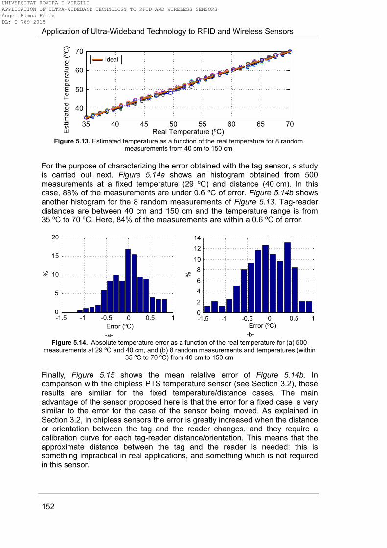
Application of Ultra-Wideband Technology to RFID and Wireless Sensors
152
40
50
60
70
Estim
ate
d T
em
pe
ratu
re (
ºC)
Ideal
35 40 45 50 55 60 65 70Real Temperature (ºC)
Figure 5.13. Estimated temperature as a function of the real temperature for 8 random
measurements from 40 cm to 150 cm
For the purpose of characterizing the error obtained with the tag sensor, a study is carried out next. Figure 5.14a shows an histogram obtained from 500 measurements at a fixed temperature (29 ºC) and distance (40 cm). In this case, 88% of the measurements are under 0.6 ºC of error. Figure 5.14b shows another histogram for the 8 random measurements of Figure 5.13. Tag-reader distances are between 40 cm and 150 cm and the temperature range is from 35 ºC to 70 ºC. Here, 84% of the measurements are within a 0.6 ºC of error.
-1.5 -1 -0.5 0 0.5 10
5
10
15
20
Error (ºC)
%
-a-
-1.5 -1 -0.5 0 0.5 10
2
4
6
8
10
12
14
Error (ºC)
%
-b-
Figure 5.14. Absolute temperature error as a function of the real temperature for (a) 500 measurements at 29 ºC and 40 cm, and (b) 8 random measurements and temperatures (within
35 ºC to 70 ºC) from 40 cm to 150 cm
Finally, Figure 5.15 shows the mean relative error of Figure 5.14b. In comparison with the chipless PTS temperature sensor (see Section 3.2), these results are similar for the fixed temperature/distance cases. The main advantage of the sensor proposed here is that the error for a fixed case is very similar to the error for the case of the sensor being moved. As explained in Section 3.2, in chipless sensors the error is greatly increased when the distance or orientation between the tag and the reader changes, and they require a calibration curve for each tag-reader distance/orientation. This means that the approximate distance between the tag and the reader is needed: this is something impractical in real applications, and something which is not required in this sensor.
UNIVERSITAT ROVIRA I VIRGILI APPLICATION OF ULTRA-WIDEBAND TECHNOLOGY TO RFID AND WIRELESS SENSORS Ángel Ramos Félix DL: T 769-2015
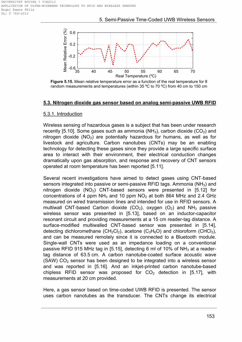
5. Semi-Passive Time-Coded UWB Wireless Sensors
153
-0.2
0.2
0.6
Mean
Rela
tive
Err
or
(%)
-0.635 40 45 50 55 60 65 70
Real Temperature (ºC) Figure 5.15. Mean relative temperature error as a function of the real temperature for 8 random measurements and temperatures (within 35 ºC to 70 ºC) from 40 cm to 150 cm
5.3. Nitrogen dioxide gas sensor based on analog semi-passive UWB RFID 5.3.1. Introduction Wireless sensing of hazardous gases is a subject that has been under research
recently [5.10]. Some gases such as ammonia (NH3), carbon dioxide (CO2) and
nitrogen dioxide (NO2) are potentially hazardous for humans, as well as for
livestock and agriculture. Carbon nanotubes (CNTs) may be an enabling
technology for detecting these gases since they provide a large specific surface
area to interact with their environment, their electrical conduction changes
dramatically upon gas absorption, and response and recovery of CNT sensors
operated at room temperature has been reported [5.11].
Several recent investigations have aimed to detect gases using CNT-based
sensors integrated into passive or semi-passive RFID tags. Ammonia (NH3) and
nitrogen dioxide (NO2) CNT-based sensors were presented in [5.12] for
concentrations of 4 ppm NH3 and 10 ppm NO2 at both 864 MHz and 2.4 GHz
measured on wired transmission lines and intended for use in RFID sensors. A
multiwall CNT-based Carbon dioxide (CO2), oxygen (O2) and NH3 passive
wireless sensor was presented in [5.13], based on an inductor-capacitor
resonant circuit and providing measurements at a 15 cm reader-tag distance. A
surface-modified multiwalled CNT-based sensor was presented in [5.14],
detecting dichloromethane (CH2Cl2), acetone (C3H6O) and chloroform (CHCl3),
and can be measured remotely since it is connected to a Bluetooth module.
Single-wall CNTs were used as an impedance loading on a conventional
passive RFID 915 MHz tag in [5.15], detecting 6 ml of 10% of NH3 at a reader-
tag distance of 63.5 cm. A carbon nanotube-coated surface acoustic wave
(SAW) CO2 sensor has been designed to be integrated into a wireless sensor
and was reported in [5.16]. And an inkjet-printed carbon nanotube-based
chipless RFID sensor was proposed for CO2 detection in [5.17], with
measurements at 20 cm provided.
Here, a gas sensor based on time-coded UWB RFID is presented. The sensor
uses carbon nanotubes as the transducer. The CNTs change its electrical
UNIVERSITAT ROVIRA I VIRGILI APPLICATION OF ULTRA-WIDEBAND TECHNOLOGY TO RFID AND WIRELESS SENSORS Ángel Ramos Félix DL: T 769-2015
Application of Ultra-Wideband Technology to RFID and Wireless Sensors
154
resistance depending on the gas concentration, in this case, nitrogen dioxide
(NO2). The CNTs change the state of the RF backscatterer. The backscatterer
used is the one based on the RF switch from Skyworks, as explained in
Section 4.4.3.
5.3.2. Carbon nanotube-based nitrogen dioxide sensor
The multiwall carbon nanotubes (MWCNT) were obtained from Nanocyl, S.A.
(Belgium). They are synthesized by chemical vapour deposition and have a
purity of over 95%. They measure up to 50 microns in length and their outer
and inner diameters range from 3 to 15 nm and 3 to 7 nm respectively. A
uniform functionalization with oxygen is applied to the carbon nanotubes
provided so as to improve their dispersion and surface reactivity. For this
activation step, the MWCNTs are placed inside a glass vessel, and a magnet,
externally controlled from the plasma chamber, is used to stir the nanotube
powder during the plasma treatment. Inductively coupled plasma at a frequency
of 13.56 MHz is used during the process. Once the MWCNT powder is placed
inside the plasma glow discharge, the treatment is performed at a pressure of
0.1 Torr, using a power of 15 W, and the processing time is adjusted to 2 min. A
controlled flow of oxygen is introduced into the chamber, which gives rise to
functional oxygen species attached to the carbon nanotube sidewalls (i. e.,
oxygenated vacancies consisting of hydroxyl, carbonyl and carboxyl groups)
[5.18]. This functionalization has been found to enhance sensitivity towards NO2
[5.11].
In the second processing step, the functionalized carbon nanotubes are dispersed in an organic vehicle (dimethylformamide), ultrasonically stirred for 20 min at room temperature and then air-brushed onto the sensor substrate while the resistance of the resulting film during deposition is controlled. Controlling film resistance during deposition enables sensors with reproducible baseline values to be obtained [5.19]. Figure 5.16 shows an image of the CNTs after the functionalization. The image is obtained with transmission electron microscopy (TEM). It shows that the morphology of the CNTs is preserved during the functionalization. Figure 5.17a shows the manufactured CNT sensor. It is deposited on Rogers RO4003C substrate (see Table 2.3). It consists of an interdigital copper structure which series-connects input and output. The MWCNT is deposited over this interdigital structure. Figure 5.17b shows the gas chamber that has been designed to house the sensor, while Figure 5.17c shows a detail of the chamber cap with the flow tubes. Figure 5.18 shows the measurement in DC (with an Agilent 34410A digital multimeter) of the CNTs for a 100 ppm of NO2 flow. As it can be observed, an absolute resistance variation of about 70 Ω is obtained.
UNIVERSITAT ROVIRA I VIRGILI APPLICATION OF ULTRA-WIDEBAND TECHNOLOGY TO RFID AND WIRELESS SENSORS Ángel Ramos Félix DL: T 769-2015

5. Semi-Passive Time-Coded UWB Wireless Sensors
155
Figure 5.16. Typical TEM microscopy image recorded on CNTs after the oxygen plasma
functionalisation
CNTs
Flow tubesa b
cFlow tubes
hh
ww
Figure 5.17. Photographs of the substrate with the CNT sensor (a), of the closed gas chamber
with the access flow tubes (b) and of the conduit with the open chamber (c). Size of the chamber: w = 23.5 mm x h = 7.35 mm
0 0.5 1 1.5 2 2.5 30
20
40
60
80
100
Time (h)
Ab
so
lute
Re
sis
tan
ce
Va
ria
tio
n (
Ω)
Air
NO2 Air
100 ppm NO2
Figure 5.18. DC measurement of the CNT absolute resistance variation for a 100 ppm of NO2
flow
Next, the behaviour of the carbon nanotube-based sensor is studied as a
function of frequency. The S-parameters of the carbon nanotubes are
measured in transmission (S21) with an Agilent E8364C VNA. Then, by using
the same calibration kit for the PTS chipless temperature sensor (see
Section 3.2.2.1), the S-parameters are dembedded [5.20], and the resistance of
the nanotubes is obtained.
Figure 5.19 shows the measurement of Figure 5.18 (repeated and connected to the VNA) as a function of frequency. The CNTs are measured for a 100 ppm of NO2 flow for 300 KHz, 2.1748 MHz and 4.0496 MHz. The shame shape as in Figure 5.18 curve is observed for 300 KHz, however the resistance variation
UNIVERSITAT ROVIRA I VIRGILI APPLICATION OF ULTRA-WIDEBAND TECHNOLOGY TO RFID AND WIRELESS SENSORS Ángel Ramos Félix DL: T 769-2015
Application of Ultra-Wideband Technology to RFID and Wireless Sensors
156
has been reduced to less than half of the DC case. If the frequency is increased up to several MHz, the variation decreases to less than 1-2 Ω.
0 0.5 1 1.5 2 2.5 3 3.5 40
10
20
30
40
Time (h)
300 kHz
2.1748 MHz
4.0496 MHz
Ab
so
lute
Re
sis
tan
ce
Va
ria
tio
n (
Ω)
Figure 5.19. CNT absolute resistance variation for a 100 ppm of NO2 flow at 300 KHz,
2.1748 MHz and 4.0496 MHz
Figure 5.20 shows the same absolute resistance variation as a function of frequency and time. As it can be observed, as the frequency increases, the variation decreases even more. A range of about 50 Ω at the 1-3 GHz range is needed for chipless resistive sensors (see Section 3.2). Given this, it is clearly noticeable that the sensor could not be read with a chipless tag as it is. Therefore, it is integrated in a semi-passive tag.
Time (h)
Fre
qu
en
cy (
MH
z)
0.5 1 1.5 2 2.5 3 3.5 4
100
200
300
400
500 0.10.10.20.20.30.30.40.40.50.50.60.60.70.7
Ab
so
lute
Re
sis
tan
ce
Va
ria
tio
n (
Ω)
Figure 5.20. CNT absolute resistance variation for a 100 ppm of NO2 flow at frequencies
between 0 and 550 MHz
Finally, Figure 5.21 shows the evolution of sensor resistance (in DC) as a function of the NO2 concentration. The first part consists of successive response-recovery cycles at increasing concentrations (10, 30, 50, 70 and 100 ppm) of NO2. Each response-recovery cycle consists of 10 minutes of exposure to diluted NO2 followed by 100 minutes recovery in dry air. A moderate baseline drift can be observed. However, the baseline is recovered in full when the duration of the cleaning cycle is increased to 140 minutes or more. Finally, the detection of 10 and 50 ppm of NO2 is also shown. It is important to stress that response and recovery experiments were performed with the sensor always operating at room temperature.
UNIVERSITAT ROVIRA I VIRGILI APPLICATION OF ULTRA-WIDEBAND TECHNOLOGY TO RFID AND WIRELESS SENSORS Ángel Ramos Félix DL: T 769-2015

5. Semi-Passive Time-Coded UWB Wireless Sensors
157
0 2 4 6 8 10 12 14 16 18 201050
1100
1150
1200
Time (h)
Se
nso
r R
esis
tan
ce
(Ω
)
10 ppm
30 ppm50 ppm
70 ppm
100 ppm
10 ppm
50 ppm
Figure 5.21. Response and recovery cycles of a CNT sensor operated at room temperature.
The evolution of sensor resistance for several concentrations of NO2 is shown
5.3.3. Wireless sensor design and calibration The designed sensor is based on the analog semi-passive UWB RFID with a switch-based UWB backscatterer (see Section 4.4.2). The UWB backscatterer uses a Vivaldi antenna, as in Section 2.5.2. Figure 5.22 shows a photograph of the tag. It is fabricated on a Rogers RO4003C substrate (see Table 2.3) and its size is 120 mm x 120 mm. All the parts are labelled. The tag is powered by a 3 V Lithium battery. Following the lines detailed in Section 4.4.2, L2 = 0 mm and the L3 round-trip delay is 850 ps. This separation is enough to detect both tag modes, given the 100 ps time resolution demonstrated in Section 2.6.1. For convenience, bearing in mind the measurements in the gas chamber, the CNT is placed on a separate board and wire-connected to the sensor tag, marked CNT in Figure 5.22a. A reference connector (marked “Ref.” in Figure 5.22a) is used to measure voltage V1 using a multimeter for sensor verification and first-time calibration.
UWB
Antenna
L1L1
Wake-up & Conditioning
2.45 GHz
Antenna
RF Switch
CNT
Ref.
UWB
Antenna
2.45 GHz Antenna
Battery
L3
L3
-a- -b-
Figure 5.22. Photograph of the fabricated tag, (a) top and (b) bottom
The calibrator circuit is based on the design described in Section 4.4.4. Figure 5.23 shows in detail the part corresponding to the conditioning circuit, which delivers a 1OUT voltage to the COM1 input of the DC switch. The COM1 voltage depends on the value of the CNT resistive sensor. This COM1 gas-
UNIVERSITAT ROVIRA I VIRGILI APPLICATION OF ULTRA-WIDEBAND TECHNOLOGY TO RFID AND WIRELESS SENSORS Ángel Ramos Félix DL: T 769-2015
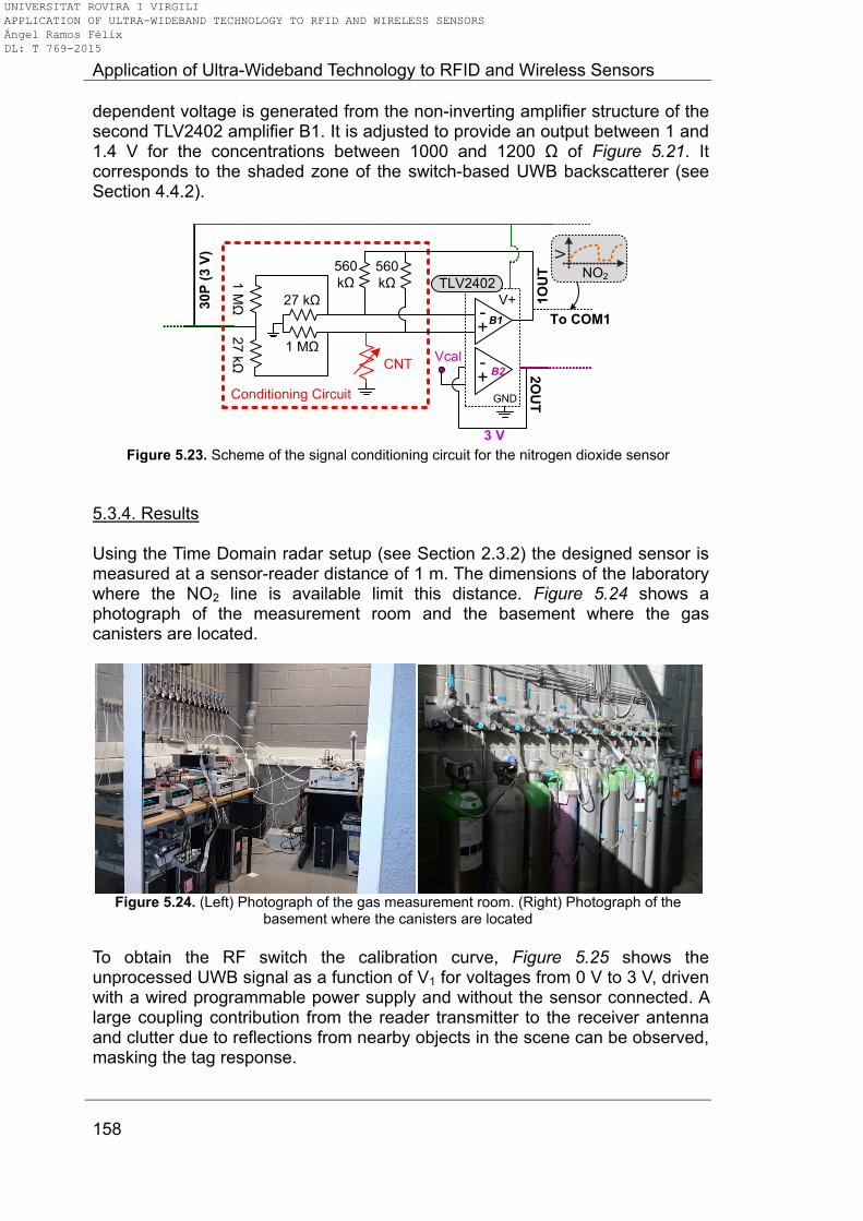
Application of Ultra-Wideband Technology to RFID and Wireless Sensors
158
dependent voltage is generated from the non-inverting amplifier structure of the second TLV2402 amplifier B1. It is adjusted to provide an output between 1 and 1.4 V for the concentrations between 1000 and 1200 Ω of Figure 5.21. It corresponds to the shaded zone of the switch-based UWB backscatterer (see Section 4.4.2).
3 V
Vcal
+-
+-
V+
GND
TLV2402
B1
B2
1O
UT
2O
UT
30P
(3 V
)
Conditioning Circuit
NO2
V
To COM1
560
kΩ
560
kΩ
1 MΩ
27 kΩ
1 M
Ω27 k
Ω CNT
Figure 5.23. Scheme of the signal conditioning circuit for the nitrogen dioxide sensor
5.3.4. Results Using the Time Domain radar setup (see Section 2.3.2) the designed sensor is measured at a sensor-reader distance of 1 m. The dimensions of the laboratory where the NO2 line is available limit this distance. Figure 5.24 shows a photograph of the measurement room and the basement where the gas canisters are located.
Figure 5.24. (Left) Photograph of the gas measurement room. (Right) Photograph of the
basement where the canisters are located
To obtain the RF switch the calibration curve, Figure 5.25 shows the unprocessed UWB signal as a function of V1 for voltages from 0 V to 3 V, driven with a wired programmable power supply and without the sensor connected. A large coupling contribution from the reader transmitter to the receiver antenna and clutter due to reflections from nearby objects in the scene can be observed, masking the tag response.
UNIVERSITAT ROVIRA I VIRGILI APPLICATION OF ULTRA-WIDEBAND TECHNOLOGY TO RFID AND WIRELESS SENSORS Ángel Ramos Félix DL: T 769-2015
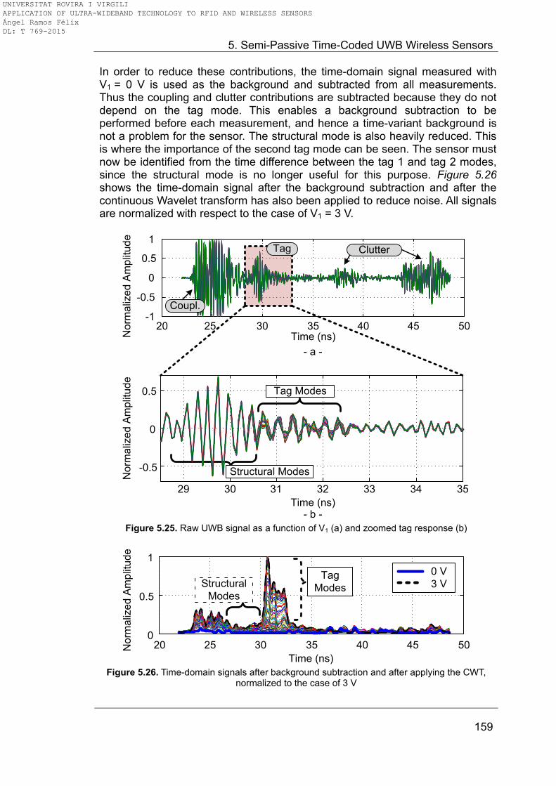
5. Semi-Passive Time-Coded UWB Wireless Sensors
159
In order to reduce these contributions, the time-domain signal measured with V1 = 0 V is used as the background and subtracted from all measurements. Thus the coupling and clutter contributions are subtracted because they do not depend on the tag mode. This enables a background subtraction to be performed before each measurement, and hence a time-variant background is not a problem for the sensor. The structural mode is also heavily reduced. This is where the importance of the second tag mode can be seen. The sensor must now be identified from the time difference between the tag 1 and tag 2 modes, since the structural mode is no longer useful for this purpose. Figure 5.26 shows the time-domain signal after the background subtraction and after the continuous Wavelet transform has also been applied to reduce noise. All signals are normalized with respect to the case of V1 = 3 V.
20 25 30 35 40 45 50-1
-0.5
0
0.5
1
Time (ns)No
rma
lize
d A
mp
litu
de
ClutterTag
Coupl.
29 30 31 32 33 34 35
-0.5
0
0.5
Time (ns)
No
rma
lize
d A
mp
litu
de
Structural Modes
Tag Modes
- a -
- b -
Figure 5.25. Raw UWB signal as a function of V1 (a) and zoomed tag response (b)
20 25 30 35 40 45 50
Time (ns)
0
0.5
1
Norm
aliz
ed
Am
plit
ud
e
0 V
3 VStructural
Modes
Tag
Modes
Figure 5.26. Time-domain signals after background subtraction and after applying the CWT,
normalized to the case of 3 V
UNIVERSITAT ROVIRA I VIRGILI APPLICATION OF ULTRA-WIDEBAND TECHNOLOGY TO RFID AND WIRELESS SENSORS Ángel Ramos Félix DL: T 769-2015
Application of Ultra-Wideband Technology to RFID and Wireless Sensors
160
Figure 5.27 shows the peaks of the tag 1 modes in Figure 5.26 as a function of V1. The peaks are also normalized to V1 = 3 V. An interpolation is calculated for the RF switch operation region using the piecewise cubic Hermite interpolating polynomial. This curve is used and stored as the sensor‟s calibration curve.
Measurement
Interpolation
0 0.5 1 1.5 2 2.5 30
0.5
1
Switch Voltage (V)
Ca
libra
ted
Tag M
od
e
Figure 5.27. Calibrated tag 1 modes as a function of V1. Interpolated calibration curve
Now, the CNT sensor is connected to the tag. Three cycles consisting of 100 ppm of NO2 for 10 min and air for 100 min are injected into the gas chamber. The results are shown in Figure 5.28. Using the calibration curve from Figure 5.27, the estimated voltage at the RF switch (V1) is obtained from the calibrated tag mode in Figure 5.28a and shown in Figure 5.28b. Voltage V1 is also measured as a reference using an Agilent 34410A multimeter. This result is also shown overlapped in Figure 5.28b. A repeatable pattern can be observed, and the wireless measurement is very close to the multimeter reference.
0 1 2 3 4 5 60
0.2
0.4
Time (h)
Calib
rate
d T
ag
Mode
-a-
0 1 2 3 4 5 6Time (h)
0.8
0.9
1
1.1
Estim
ate
d S
witch
Vo
ltage (
V)
Multimeter Ref.
Wireless
Air (100 min)100 ppm NO2 (10 min)
Base line (10 min)
-b-
Figure 5.28. (a) Calibrated tag mode as a function of time for a varying CNT sensor.(b) Estimated switch voltage V1 as a function of time for three measurement cycles of 100 ppm
NO2 compared to measured voltage V1
UNIVERSITAT ROVIRA I VIRGILI APPLICATION OF ULTRA-WIDEBAND TECHNOLOGY TO RFID AND WIRELESS SENSORS Ángel Ramos Félix DL: T 769-2015
5. Semi-Passive Time-Coded UWB Wireless Sensors
161
In order to detect several concentrations of NO2, the measurement profile from Section 5.3.2 (see Figure 5.21) is chosen. The results are shown in Figure 5.29. Figure 5.30 shows the relative error of the wireless measurement with respect to the multimeter reference as a function of time. The mean relative error is 0.34%. To derive the sensitivity of the sensor, Figure 5.31 shows the relative resistance change obtained from the measurements in Figure 5.29. Relative changes of 3.9%, 9.2%, 14%, 16.6%, and 19.9% are obtained for 10, 30, 50, 70 and 100 ppm respectively.
0 2 4 6 8 10 12 14 16 18 200.9
1
1.1
1.2
1.3
Time (h)
Estim
ate
d S
witch
Vo
ltage (
V)
Wireless
Multimeter Reference10 ppm
50 ppm
30 ppm
70 ppm 100 ppm
10 ppm
50 ppm
Figure 5.29. Estimated switch voltage as a function of time for 10, 30, 50, 70 and 100 ppm
concentrations of NO2 compared to the wired reference
0 5 10 15 20-2
-1
0
1
2
Time (h)
Re
lative
Err
or
(%)
Mean: 0.34%
Figure 5.30. Relative error between the wired reference and the wireless measurement
0 2 4 6 8 10 12 14 16 18 200
5
10
15
20
Time (h)
Re
lative
Resis
tance C
hange
(%
)
WirelessMultim. Ref.
10
30
5070 100
10
50
Figure 5.31. Relative resistance change as a function of NO2 concentration
UNIVERSITAT ROVIRA I VIRGILI APPLICATION OF ULTRA-WIDEBAND TECHNOLOGY TO RFID AND WIRELESS SENSORS Ángel Ramos Félix DL: T 769-2015
Application of Ultra-Wideband Technology to RFID and Wireless Sensors
162
5.4. Sensor integration in microcontroller-based semi-passive UWB RFID An alternative for wireless UWB sensors with the digital microcontroller-based approach is shown here. As explained in Section 4.3.6, the digital tag can integrate both analog and digital sensors easily. To this end, two systems are proposed:
A multi-sensor tag which integrates analog DC and digital I2C sensors, for smart cities applications
A nitrogen dioxide (NO2) digital sensor tag
5.4.1. Multi-sensor tag
The block diagram of the multi-sensor tag is shown in Figure 5.32. It consists of a core logic based on the PIC 16F1827, a wake-up circuit to detect the signal coming from the 2.45 GHz modulator, a UWB backscatterer, which performs the communication between the tag and the reader and the sensor module. This module can be divided into two parts, those sensors which are connected directly to the analog-to-digital converters of the PIC and those sensors which are connected to the PIC by means of an I2C interface. The sensors connected to the microcontroller ADC consist of a Texas Instruments TMP20 temperature sensor and a HoneyWell HIH-5031 humidity sensor. The sensors connected to the I2C bus consist of a FreeScale MMA8453QT accelerometer and a MPL115A2T1 barometer. A Microchip 24LC256 non-volatile EEPROM memory is also connected to the I2C bus to store measurements. This is a key feature in those applications where the sensor and the reader are not in continuous connection. It permits to store measurements which are downloaded when the sensor and the reader are under connection.
UWB
Backscatterer
Accelerometer
MMA8453QT
Barometer
MPL115A2T1
EEPROM
24LC256
2.45 GHz
Wake-up
Core Logic
PIC16F1827
ADC
Humidity
HIH-5031
Temperature
TMP20
Long- term storage
I2C
Figure 5.32. Block diagram of the multi-sensor tag
Figure 5.33 shows a vertical cut and photographs of the sensor tag. Its size is
12 cm x 6 cm and it is fabricated on Rogers RO4003C (see Table 2.3). It is
powered using a 3 V Lithium battery. As shown in the vertical cut, the
multisensor module is manufactured on a separate board which is overlaped to
the tag board, as also shown in Figure 5.33.
UNIVERSITAT ROVIRA I VIRGILI APPLICATION OF ULTRA-WIDEBAND TECHNOLOGY TO RFID AND WIRELESS SENSORS Ángel Ramos Félix DL: T 769-2015

5. Semi-Passive Time-Coded UWB Wireless Sensors
163
Wake-up module Core logic UWB backscatterer
multi-sensor module
Front
Back
Temperature
Sensors
Multi-sensor module
Humidity
Sensor
EEPROM
BarometerAccelerometer
Figure 5.33. Vertical cut of the multi-sensor tag and photographs of the front and back faces of
the tag, and of the multi-sensor module board
As an example, the measurement of tempeature with the TMP20 sensor and of acceleration with the MMA8453QT sensor is shown next. Figure 5.34 shows a measurement of the differential signal (see Section 4.3.4) as a function of time. The inset shows the signal prior to applying processing. On top of this, the CWT (see Section 2.4.2) is applied to increase the signal-to-noise ratio.
20 25 30 35 40 45 500
0.2
0.4
0.6
0.8
1
Time (ns)
No
rma
lized
Am
plit
ud
e
20 25 30 35 40 45 50-1
0
1
Time (ns)
No
rm.
Am
pl.
Figure 5.34. Differential signal of a multi-sensor tag read after applying processing. In the
inset, RAW signal before processing
Figure 5.35 shows the signal sequences corresponding to two measurements of temperature at 50 cm. The first measurement (top) is 24.91 ºC, the second 108.79 ºC. Temperature has been also obtained by wired means as a reference to validate the system. The measured values are 24.516 ºC and 107.8474 ºC. The reference of the MMA8453QT accelerometer is read using the FreeScale Sensor Toolbox. The orientation bits from the PL_STATUS register are considered: LAPO and BAFRO. LAPO indicates whether the sensor is in a landscape or portrait orientation. BAFRO indicates if the sensor is in a back or front orientation. The accelerometer functionality is tested by just changing the sensor position. Figure 5.36 shows a photograph of the sensor next to the read for the front, portrait up (LAPO=„00‟, BAFRO=„0‟) orientation.
UNIVERSITAT ROVIRA I VIRGILI APPLICATION OF ULTRA-WIDEBAND TECHNOLOGY TO RFID AND WIRELESS SENSORS Ángel Ramos Félix DL: T 769-2015

Application of Ultra-Wideband Technology to RFID and Wireless Sensors
164
26
28
30
00..22
00..44
00..66
00..88
Differential Signal Bit Number
Tim
e (
ns)
2 4 6 8 10
29
31
24.91 ºC24.91 ºC
108.79 ºC108.79 ºC
Figure 5.35. Differential signal sequence for two temperature measurements
g
Figure 5.36. Accelerometer read for the front, portrait up orientation
5.4.2. Nitrogen dioxide gas sensor Based on the same carbon nanotube gas resistive sensor presented in Section 5.3, an alternative of the same sensor integrated in a digital tag is shown next. Figure 5.37 shows a photograph of the manufactured tag. It uses the same backscatterer and monopole configuration proposed in Section 4.3. Figure 5.38 shows the circuit scheme of the tag with the conditioing circuit to convert the resistance to a voltage drop. The same conditioning circuit presented in Section 5.3.3 is used (with a single TLV2401 operational amplifier). In this case the conditioning circuit output is connected to the PIC‟s analog-to-digital converter (ADC, RA1). The range of operation of this circuit (between 1 and 1.4 V) falls inside the ADC‟s requirements (0 V to 3 V). Moreover, if the sensor resistance baseline drifts, which may happen during a long-time measurement (see Section 5.3.4), the output values still have room to reach one of the boundaries (0 or 3 V). The conditioning circuit is powered from the PIC itself, using a digital output (RA4). This is an advantage, since the sensor only drains power when it is being read by the tag. The sensor is operated at room temperature (i.e., 25 ºC) throughout the whole test procedure. The moisture level is kept constant at 10% relative humidity (R. H.) The test exercise involved 4 CNT sensors (to assess sensor reproducibility) and a measurement period of over 250 h at the end of which, sensors remained fully functional. The baseline resistance of the sensors (@25 ºC and 10% R. H. in air) was about 1400 Ω. Figure 5.39 shows a comparison between the response of a wired measurement (with an Agilent
UNIVERSITAT ROVIRA I VIRGILI APPLICATION OF ULTRA-WIDEBAND TECHNOLOGY TO RFID AND WIRELESS SENSORS Ángel Ramos Félix DL: T 769-2015
5. Semi-Passive Time-Coded UWB Wireless Sensors
165
34410A multimeter in parallel) and a wireless measurement. The wired measurement is obtained only once and is used for comparing the performance of the wireless system. The actual physical parameter that the sensor changes is its electrical resistance (RCNT in Ω). The following conversion factor can be applied to the detected voltage VADC in order to obtain the resistance:
414.07 · 696.88 CNT ADCR V . The margin 1.25 – 1.7 V from Figure 5.39
corresponds to, approximately, 1215 – 1400 Ω. The concentrations of NO2 applied to the sensor in each measurement are marked out.
UW
B B
ackscat.
UW
B B
ackscat.
Wake-upWake-up LogicLogic
CNTCNT
Gas ChamberGas Chamber
Figure 5.37. Photograph of the manufactured digital nitrogen dioxide sensor tag
+-
V+
GND
TLV2401
Conditioning Circuit
NO2
V560
kΩ
560
kΩ
1 MΩ
27 kΩ1
MΩ
27
kΩ CNT
GND
RA4RA1
VCC 3 V
Lithium
Battery
To ADC
PIC16F1827
‘1’
(3
V)
‘1’
(3
V)
Figure 5.38. Scheme of the circuit between the PIC16F1827 and the CNT sensor
Figure 5.40 shows the absolute error between the wired reference and the wireless measurement. The mean error is also shown, with a value of 4.5 mV. Theoretically, the analog-to-digital converter of the tag (a 10-bit resolution ADC embedded in a Microchip PIC16F1827 microcontroller) has a quantization error QErr. of:
10
3 0. 2.93 mV
10242CCV GND
QErr
. (5.5)
The mean error is therefore close to the theoretical limit. The relative error remains mostly below 1%, never exceeds 2% and its mean value is 0.29%. Although some baseline drift can be observed in the response of the sensor to high nitrogen dioxide concentrations (e.g., see the repeated response-recovery
UNIVERSITAT ROVIRA I VIRGILI APPLICATION OF ULTRA-WIDEBAND TECHNOLOGY TO RFID AND WIRELESS SENSORS Ángel Ramos Félix DL: T 769-2015
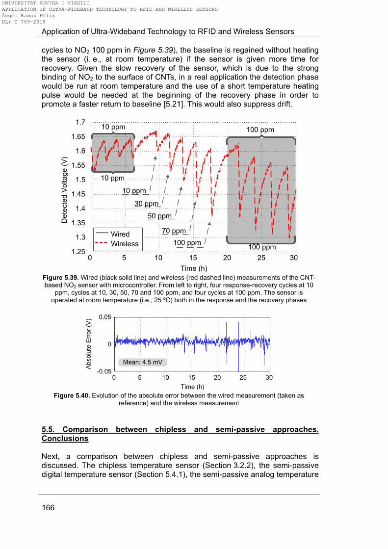
Application of Ultra-Wideband Technology to RFID and Wireless Sensors
166
cycles to NO2 100 ppm in Figure 5.39), the baseline is regained without heating the sensor (i. e., at room temperature) if the sensor is given more time for recovery. Given the slow recovery of the sensor, which is due to the strong binding of NO2 to the surface of CNTs, in a real application the detection phase would be run at room temperature and the use of a short temperature heating pulse would be needed at the beginning of the recovery phase in order to promote a faster return to baseline [5.21]. This would also suppress drift.
0 5 10 15 20 25 301.25
1.3
1.35
1.4
1.45
1.5
1.55
1.6
1.65
1.7
Time (h)
De
tecte
d V
olta
ge
(V
)
10 ppm
30 ppm
50 ppm
70 ppm
100 ppm
10 ppm
10 ppm
Wired
Wireless
100 ppm
100 ppm
Figure 5.39. Wired (black solid line) and wireless (red dashed line) measurements of the CNT-based NO2 sensor with microcontroller. From left to right, four response-recovery cycles at 10
ppm, cycles at 10, 30, 50, 70 and 100 ppm, and four cycles at 100 ppm. The sensor is operated at room temperature (i.e., 25 ºC) both in the response and the recovery phases
0 5 10 15 20 25 30
Time (h)
-0.05
0
0.05
Ab
so
lute
Err
or
(V)
Mean: 4.5 mV
Figure 5.40. Evolution of the absolute error between the wired measurement (taken as
reference) and the wireless measurement
5.5. Comparison between chipless and semi-passive approaches. Conclusions Next, a comparison between chipless and semi-passive approaches is discussed. The chipless temperature sensor (Section 3.2.2), the semi-passive digital temperature sensor (Section 5.4.1), the semi-passive analog temperature
UNIVERSITAT ROVIRA I VIRGILI APPLICATION OF ULTRA-WIDEBAND TECHNOLOGY TO RFID AND WIRELESS SENSORS Ángel Ramos Félix DL: T 769-2015
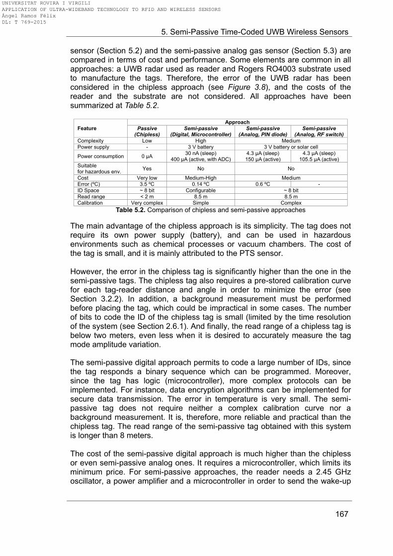
5. Semi-Passive Time-Coded UWB Wireless Sensors
167
sensor (Section 5.2) and the semi-passive analog gas sensor (Section 5.3) are compared in terms of cost and performance. Some elements are common in all approaches: a UWB radar used as reader and Rogers RO4003 substrate used to manufacture the tags. Therefore, the error of the UWB radar has been considered in the chipless approach (see Figure 3.8), and the costs of the reader and the substrate are not considered. All approaches have been summarized at Table 5.2.
Feature Approach
Passive (Chipless)
Semi-passive (Digital, Microcontroller)
Semi-passive (Analog, PIN diode)
Semi-passive (Analog, RF switch)
Complexity Low High Medium
Power supply - 3 V battery 3 V battery or solar cell
Power consumption 0 μA 30 nA (sleep)
400 μA (active, with ADC) 4.3 μA (sleep) 150 μA (active)
4.3 μA (sleep) 105.5 μA (active)
Suitable for hazardous env.
Yes No No
Cost Very low Medium-High Medium
Error (ºC) 3.5 ºC 0.14 ºC 0.6 ºC -
ID Space ~ 8 bit Configurable ~ 8 bit
Read range < 2 m 8.5 m 8.5 m
Calibration Very complex Simple Complex
Table 5.2. Comparison of chipless and semi-passive approaches
The main advantage of the chipless approach is its simplicity. The tag does not require its own power supply (battery), and can be used in hazardous environments such as chemical processes or vacuum chambers. The cost of the tag is small, and it is mainly attributed to the PTS sensor. However, the error in the chipless tag is significantly higher than the one in the semi-passive tags. The chipless tag also requires a pre-stored calibration curve for each tag-reader distance and angle in order to minimize the error (see Section 3.2.2). In addition, a background measurement must be performed before placing the tag, which could be impractical in some cases. The number of bits to code the ID of the chipless tag is small (limited by the time resolution of the system (see Section 2.6.1). And finally, the read range of a chipless tag is below two meters, even less when it is desired to accurately measure the tag mode amplitude variation.
The semi-passive digital approach permits to code a large number of IDs, since the tag responds a binary sequence which can be programmed. Moreover, since the tag has logic (microcontroller), more complex protocols can be implemented. For instance, data encryption algorithms can be implemented for secure data transmission. The error in temperature is very small. The semi-passive tag does not require neither a complex calibration curve nor a background measurement. It is, therefore, more reliable and practical than the chipless tag. The read range of the semi-passive tag obtained with this system is longer than 8 meters. The cost of the semi-passive digital approach is much higher than the chipless or even semi-passive analog ones. It requires a microcontroller, which limits its minimum price. For semi-passive approaches, the reader needs a 2.45 GHz oscillator, a power amplifier and a microcontroller in order to send the wake-up
UNIVERSITAT ROVIRA I VIRGILI APPLICATION OF ULTRA-WIDEBAND TECHNOLOGY TO RFID AND WIRELESS SENSORS Ángel Ramos Félix DL: T 769-2015

Application of Ultra-Wideband Technology to RFID and Wireless Sensors
168
commands. The battery at the tag limits it to be used in hazardous environments. Moreover, there is power consumption due to the elements at the tag. In sleep mode, the only consuming element is the microcontroller, which consumes 30 nA (see Section 4.3). In active mode, however, the microcontroller consumes 75 μA, added to the PIN diode when it is „on‟, which consumes 70 μA, and the TMP20, which accounts for 4 μA, and about 250 μA of the ADC, totalling a 400 μA consumption of the tag. This value, even though it is considerably low for a semi-passive tag given its features, contrasts with the zero value of the chipless approach. The semi-passive analog approaches require less power because no ADC is used. However, the standby current is larger.
In conclusion, depending on the application and its constraints (precision, number of sensors deployed, hazardous environment, distance), it will be more suitable to use one approach or the other.
5.6. Bibliography [5.1] J. Yin, J. Yi, M. K. Law, et al. “A System-on-Chip EPC Gen-2 Passive UHF RFID Tag
With Embedded Temperature Sensor,” IEEE Journal of Solid-State Circuits, Vol. 45, No. 11, pp. 2404-2420, Nov. 2010.
[5.2] F. Kocer and M. P. Flynn, “An RF-powered, wireless CMOS temperature sensor,” IEEE
Sensors Journal, Vol. 6, No. 3, pp. 557-564, 2006. [5.3] R. Vykas, V. Lakafosis, A. Rida, N. Chaisilwattana, S. Travis, J. Pan, and M. M.
Tentzeris, “Paper-Based RFID-Enabled Wireless Platforms for Sensing Applications,” IEEE Transactions on Microwave Theory and Techniques, Vol. 57, No. 5, pp. 1370-1382, 2009.
[5.4] N. Cho, S-J. Song, S. Kim, S. Kim, and H-J. Yoo, "A 5.1-μW UHF RFID tag chip
integrated with sensors for wireless environmental monitoring," Proc. 31st European Solid-State Circuits Conference 2005, pp. 279-282, 2005.
[5.5] S. Kim, A. Georgiadis, A. Collado, and M. M. Tentzeris, “An Inkjet-Printed Solar-
Powered Wireless Beacon on Paper for Identification and Wireless Power Transmission Applications,” IEEE Transactions on Microwave Theory and Techniques, Vol. 60, No. 12, Part. 2, pp. 4178-4186, 2012.
[5.6] A. Georgiadis, A. Collado, S. Kim, L. Hoseon, and M. M. Tentzeris, “UHF solar powered
active oscillator antenna on low cost flexible substrate for wireless identification applications,” 2012 IEEE MTT-S International Microwave Symposium Digest, pp. 1-3, 2012.
[5.7] American Society for Testing and Materials (ASTM) Terrestrial Reference Spectra for
Photovoltaic Performance Evaluation, http://rredc.nrel.gov/solar/spectra/am1.5/
[5.8] M. Tanaka, R. Suzuki, Y. Suzuki, and K. Araki, “Microstrip antenna with solar cells for microsatellites,” Proc. 1994 IEEE International Symposium on Antennas and Propagation (AP-S), Vol. 2, pp. 786-789, June 1994.
[5.9] A. Collado and A. Georgiadis, "Conformal Hybrid Solar and Electromagnetic (EM)
Energy Harvesting Rectenna," IEEE Transactions on Circuits and Systems I: Regular Papers, Vol. 60, No. 8, pp. 2225-2334, 2013.
UNIVERSITAT ROVIRA I VIRGILI APPLICATION OF ULTRA-WIDEBAND TECHNOLOGY TO RFID AND WIRELESS SENSORS Ángel Ramos Félix DL: T 769-2015
5. Semi-Passive Time-Coded UWB Wireless Sensors
169
[5.10] T. T. Thai, L. Yang, G. R. DeJean, and M. M. Tentzeris, “Nanotechnology Enables
Wireless Gas Sensing,” IEEE Microwave Magazine, pp. 84-95, 2011.
[5.11] Z. Zanolli, R. Leghrib, A. Felten, J-J. Pireaux, E. Llobet, and J-C. Charlier, “Gas Sensing with Au-Decorated Carbon Nanotubes,” ACS Nano, 5, Vol. 6, pp. 4529-4599, 2011.
[5.12] V. Lakafosis, Y. Xiaohua, L. Taoran, E. Gebara, W. Yang, and M. M. Tentzeris, “Wireless sensing with smart skins,” Proc. 2011 IEEE Sensors, pp. 623-626, 2011.
[5.13] K. G. Ong, K. Zeng, and C. A. Grimes, “A Wireless, Passive Carbon Nanotube-Based Gas Sensor,” IEEE Sensors Journal, Vol. 2, No. 2, pp. 82-88 2002.
[5.14] J. K. Abraham, B. Philip, A. Witchurch, V. K. Varadan, and C. C. Reddy, “A compact wireless gas sensor using a carbon nanotube/PMMA thin film chemiresistor,” Smart Mater. Struct., Vol. 13, No. 5, pp. 1045–1049, 2004.
[5.15] C. Occhiuzzi, A. Rida, G. Marrocco, and M. M. Tentzeris, "RFID Passive Gas Sensor Integrating Carbon Nanotubes,” IEEE Transactions on Microwave Theory and Techniques, Vol. 59, No. 10, pp. 2674-2684. 2011.
[5.16] S. Sivaramakrishnan, R. Rajamani, C. S. Smith, K. A. McGee, K. R. Mann, and N. Yamashita, “Carbon nanotube-coated surface acoustic wave sensor for carbon dioxide sensing,” Sensors and Actuators B, Vol. 132, pp. 296-304, 2008.
[5.17] A. Vena, L. Sydänheimo, M. M. Tentzeris, and L. Ukkonen, “A Novel Inkjet Printed Carbon Nanotube-Based Chipless RFID Sensor for Gas Detection,” Proc. of the 43rd European Microwave Conference, 2013.
[5.18] R. Ionescu, E.H. Espinosa, E. Sotter, E. Llobet, X. Vilanova, X. Correig, A. Felten, C. Bittencourt, G. Van Lier, J.C. Charlier, and J.J. Pireaux, “Oxygen functionalisation of MWNT and their use as gas sensitive thick-film layers”, Sensors and Actuators B, 113, pp.36-46, 2006.
[5.19] I. Hafaiedh, W. Elleuch, P. Clement, E. Llobet, A. Abdelghani, “Multi-walled carbon nanotubes for volatile organic compound detection”, Sensors and Actuators B: Chemical, Vo. 182, pp. 344-350, June 2013.
[5.20] Agilent Technologies, “De-embedding and Embedding S-Parameter Networks Using a Vector Network Analyzer,” Application Note 1364-1, 2004.
[5.21] R. Leghrib, A. Felten, F. Demoisson, F. Reniers, J-J. Pireaux, and E. Llobet, "Room-temperature, selective detection of benzene at trace levels using plasma-treated metal-decorated multiwalled carbon nanotubes," Carbon, Vol. 48, No. 12, pp. 3477-344, 2010.
UNIVERSITAT ROVIRA I VIRGILI APPLICATION OF ULTRA-WIDEBAND TECHNOLOGY TO RFID AND WIRELESS SENSORS Ángel Ramos Félix DL: T 769-2015

Application of Ultra-Wideband Technology to RFID and Wireless Sensors
170
UNIVERSITAT ROVIRA I VIRGILI APPLICATION OF ULTRA-WIDEBAND TECHNOLOGY TO RFID AND WIRELESS SENSORS Ángel Ramos Félix DL: T 769-2015
6. Smart Floor Applications using Time-Coded UWB RFID and GPR
171
6. Smart Floor Applications using Time-Coded UWB RFID and Ground Penetrating Radar 6.1. Introduction RFID can be used to locate or guide autonomous entities, such as robots or people, within a defined surface. To this end, tags are scattered in a given space and then an RFID reader is placed on the mobile subject in order to identify the position inside that space, based on a previous tag mapping of the environment [6.1-6.6]. This concept is often referred to as smart floor [6.7]. Several RFID approaches have been investigated for this application [6.1-6.8] and low-cost passive tags are preferred [6.7]. For instance, 13.56 MHz tags are used in [6.7-6.8], while UHF passive tags are used in [6.6]. The proposed time-coded UWB RFID systems can be an alternative for smart floors and indoor localization aplplications. Since they are based in time-domain, an easy localization is possible using the delay information. In addition, as explained in Section 2.6.3, time-coded UWB RFID tags are not heavily affected by the material they are attached to. Therefore, they can be embedded in different types of floor. This chapter performs a study on the feasibility of using time-coded UWB RFID tags and its combination with ground penetrating radar (GPR) techniques for indoor mapping, localization and guidance. To this end, three types of tags are considered:
1. Passive reflectors, made of metallic strips 2. Chipless time-coded UWB tags, as the ones developed in Chapter 2 3. Semi-passive time-coded UWB tags (see Section 4.3)
Since the UWB radar used as reader transmits a pulse and the tag responds by backscattering, the time-of-arrival (TOA) can be measured without the need of any synchronization system implemented in the tag. This chapter is organized as follows:
Section 6.2 proposes the alternatives for smart floor design
Section 6.3 presents the obtained results for the passive reflectors, and the chipess and semi-passive time-coded UWB tags
Finally, Section 6.4 draws the conclusions
6.2. Smart floor design. Alternatives
The tag-reader system that has been designed is shown in Figure 6.1a. The reader is based on the bistatic UWB radar Time Domain PulsON P400 MRM (see Section 2.3.2). It is connected to two UWB antennas (Tx and Rx) that illuminate the smart floor, which is shown in Figure 6.1b. The smart floor consists of ceramic tiles with a total size of 1 x 2 meters. It has been
UNIVERSITAT ROVIRA I VIRGILI APPLICATION OF ULTRA-WIDEBAND TECHNOLOGY TO RFID AND WIRELESS SENSORS Ángel Ramos Félix DL: T 769-2015
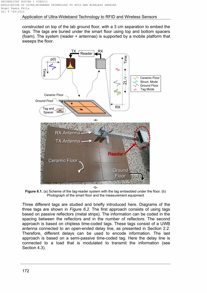
Application of Ultra-Wideband Technology to RFID and Wireless Sensors
172
constructed on top of the lab ground floor, with a 3 cm separation to embed the tags. The tags are buried under the smart floor using top and bottom spacers (foam). The system (reader + antennas) is supported by a mobile platform that sweeps the floor.
Tim
e2
L/v
Tim
e
p(t)
TXReader
RX
Ceramic Floor
Ground Floor
Ceramic FloorGround FloorStruct. Mode
Ceramic Floor
Ground Floor
Tag Mode
Tag and
Spacer
RX
-a-
Ceramic FloorCeramic Floor
Ground
Floor
Ground
Floor
Reader Reader
TX AntennaTX Antenna
RX AntennaRX Antenna
-b-
Figure 6.1. (a) Scheme of the tag-reader system with the tag embedded under the floor. (b) Photograph of the smart floor and the measurement equipment
Three different tags are studied and briefly introduced here. Diagrams of the three tags are shown in Figure 6.2. The first approach consists of using tags based on passive reflectors (metal strips). The information can be coded in the spacing between the reflectors and in the number of reflectors. The second approach is based on chipless time-coded tags. These tags consist of a UWB antenna connected to an open-ended delay line, as presented in Section 2.2. Therefore, different delays can be used to encode information. The last approach is based on a semi-passive time-coded tag. Here the delay line is connected to a load that is modulated to transmit the information (see Section 4.3).
UNIVERSITAT ROVIRA I VIRGILI APPLICATION OF ULTRA-WIDEBAND TECHNOLOGY TO RFID AND WIRELESS SENSORS Ángel Ramos Félix DL: T 769-2015
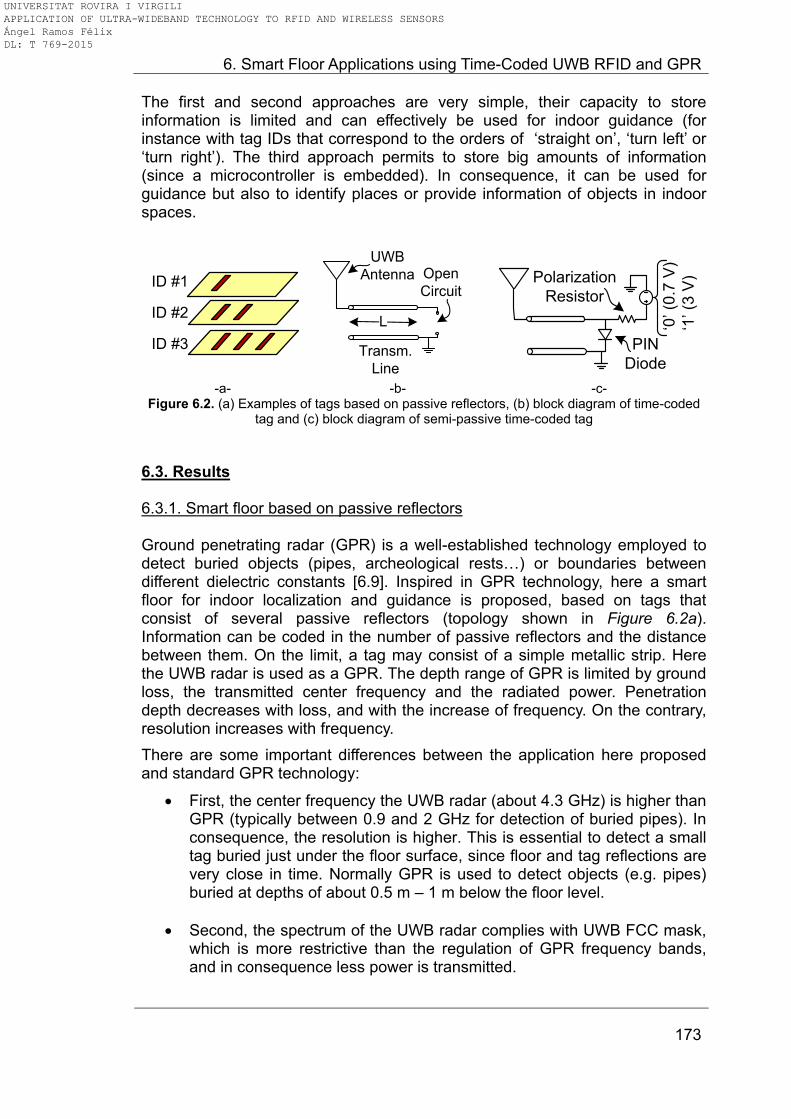
6. Smart Floor Applications using Time-Coded UWB RFID and GPR
173
The first and second approaches are very simple, their capacity to store information is limited and can effectively be used for indoor guidance (for instance with tag IDs that correspond to the orders of „straight on‟, „turn left‟ or „turn right‟). The third approach permits to store big amounts of information (since a microcontroller is embedded). In consequence, it can be used for guidance but also to identify places or provide information of objects in indoor spaces.
ID #1
ID #2
ID #3
L
UWB
Antenna
Transm.
Line
Open
Circuit
Polarization
Resistor
PIN
Diode
„0‟ (0
.7 V
)
„1‟ (3
V)
-a- -b- -c- Figure 6.2. (a) Examples of tags based on passive reflectors, (b) block diagram of time-coded
tag and (c) block diagram of semi-passive time-coded tag
6.3. Results 6.3.1. Smart floor based on passive reflectors Ground penetrating radar (GPR) is a well-established technology employed to detect buried objects (pipes, archeological rests…) or boundaries between different dielectric constants [6.9]. Inspired in GPR technology, here a smart floor for indoor localization and guidance is proposed, based on tags that consist of several passive reflectors (topology shown in Figure 6.2a). Information can be coded in the number of passive reflectors and the distance between them. On the limit, a tag may consist of a simple metallic strip. Here the UWB radar is used as a GPR. The depth range of GPR is limited by ground loss, the transmitted center frequency and the radiated power. Penetration depth decreases with loss, and with the increase of frequency. On the contrary, resolution increases with frequency.
There are some important differences between the application here proposed and standard GPR technology:
First, the center frequency the UWB radar (about 4.3 GHz) is higher than GPR (typically between 0.9 and 2 GHz for detection of buried pipes). In consequence, the resolution is higher. This is essential to detect a small tag buried just under the floor surface, since floor and tag reflections are very close in time. Normally GPR is used to detect objects (e.g. pipes) buried at depths of about 0.5 m – 1 m below the floor level.
Second, the spectrum of the UWB radar complies with UWB FCC mask, which is more restrictive than the regulation of GPR frequency bands, and in consequence less power is transmitted.
UNIVERSITAT ROVIRA I VIRGILI APPLICATION OF ULTRA-WIDEBAND TECHNOLOGY TO RFID AND WIRELESS SENSORS Ángel Ramos Félix DL: T 769-2015
Application of Ultra-Wideband Technology to RFID and Wireless Sensors
174
Third, GPR antennas are generally in close proximity to the surface. The strong reflection on the surface can be deleted using a time-window since, as explained, generally the buried objects are far from the surface. In the proposed application, the tag is very close to the floor and the tag response cannot be easily filtered. In order to avoid the blind distance effect, the antennas are air-launched allowing for filtering the signal coupled between TX and RX antennas.
Fourth, small, portable and low-cost CMOS UWB radars (see Section 2.3.2) are commercially available and suitable for this application, compared with heavy and expensive GPR equipment.
Simulations are obtained using the finite-difference time-domain method (FDTD) [6.10]. The simulated scenario consists of a floor of 1 cm thick ceramic tiles (εr = 6). A perfect electrical conductor (PEC) sheet is buried between the floor and the ground (which are separated 5 cm). The ground is simulated with a dielectric permittivity close to dry sand (εr = 3). A spacer of 1 cm is considered in order to simulate the experimental test bed scenario. The Tx and Rx antennas are separated 10 cm between them, and the radar scans a distance of 1 m. Figure 6.3 shows the raw (unprocessed) data for the cases of two individual PEC sheets 10 and 20 cm wide. Figure 6.4 shows the results after clutter removal by applying background subtraction. Clutter is mainly due to antenna coupling and reflection at the floor surface. It is removed by using the average of the image in cross-range [6.11]. This background subtraction can be done dynamically using a moving averaging filter, as described in [6.11]. After removing clutter, the position of the reflector can be easily obtained. The typical hyperbola shape like in GPR systems can be observed [6.10]. The maximum is located at the center of the reflector. The depth of the reflector can be estimated from the delay at the maximum point and the propagation velocity of the medium from the aperture of the hyperbola. Figure 6.5 shows the simulated raw data for two sheets 10 cm wide separated 30 cm and 50 cm, respectively. Figure 6.6 shows the same simulation after background subtraction. It can be observed that a ghost reflection appears between the two sheets and at a larger delay due to the coupling between the two reflections. The intensity of this ghost reflection is increased when the spacing between the reflectors is reduced.
Concerning measurements, as an example three tag IDs (as shown in Figure 6.2a) are measured by considering one, two or three metallic sheets with different widths (15 / 10 / 20 cm), separated 25 cm. Figure 6.7 shows the measured raw data. It can be observed that the raw data is enough to detect the position and the hyperbolas corresponding to the metal sheets. This is an interesting result since it means that no background subtraction is required for this application and in consequence, inhomogeneities in the floor are supported.
UNIVERSITAT ROVIRA I VIRGILI APPLICATION OF ULTRA-WIDEBAND TECHNOLOGY TO RFID AND WIRELESS SENSORS Ángel Ramos Félix DL: T 769-2015

6. Smart Floor Applications using Time-Coded UWB RFID and GPR
175
Position (cm)
De
lay(n
s)
-50 0 50
0
5
10
-1
-0.5
0
Position (cm)
-50 0 50
-a- -b-
Figure 6.3. Simulated raw data for a single PEC sheet of width (a) 10 cm and (b) 20 cm
Position (cm)
De
lay(n
s)
-50 0 50
0
5
10
-0.5
0
0.5
1
Position (cm)
-50 0 50
-a- -b- Figure 6.4. Simulated data for a single PEC sheet of width (a) 10 cm and (b) 20 cm, after
background subtraction
Position (cm)
-50 0 50
-1
-0.5
0
Position (cm)
De
lay(n
s)
-50 0 50
0
5
10
-a- -b-
Figure 6.5. Simulated raw data for two PEC sheets of width 10 cm, separated (a) 30 cm and (b) 50 cm
UNIVERSITAT ROVIRA I VIRGILI APPLICATION OF ULTRA-WIDEBAND TECHNOLOGY TO RFID AND WIRELESS SENSORS Ángel Ramos Félix DL: T 769-2015

Application of Ultra-Wideband Technology to RFID and Wireless Sensors
176
Position (cm)
De
lay(n
s)
-50 0 50
0
5
10
Position (cm)
-50 0 50
-0.5
0
0.5
1
-a- -b- Figure 6.6. Simulated data for two PEC sheets of width 10 cm, separated 30 cm (a) and 50 cm
(b), after background subtraction.
6.3.2. Smart floor based on chipless time-coded UWB RFID tags It can be observed in Figure 6.1a that a long delay line connected to the UWB
antenna is required to separate the tag mode from the reflections at the ground.
To this end, two tags have been emulated using a UWB antenna and coaxial
delay lines connected to an RF switch. In this manner, the minimum delay
required to separate the tag mode can be studied.
Figure 6.8 shows the two time-coded chipless UWB RFID tags read under the
floor structure. The tag modes are marked with red arrows. Background
subtraction is applied for clutter removal. As it can be observed, depending on
the tag ID (length of the delay line) the tag mode appears at a different time.
Since the tag has a small RCS compared to a metal sheet, it is difficult to detect
the hyperbola shape in this case, and the estimation of the position of the tag is
more inaccurate. However, for identification purposes, the tag can be read. A
combination of this approach with the passive reflectors (see Section 6.3.1),
which could be realized by simply increasing the RCS of the tag adding a metal
strip, would lead to the possibility of a better tag detection (structural mode).
Figure 6.9 shows a cut for the maximum position index for both tags from
Figure 6.8, in this case at 59.34 cm from the beginning of the smart floor. The
difference between the tag mode delays can be clearly observed. In addition,
the peaks corresponding to the ceramic floor, ground floor and structural modes
are also observed.
In order to detect the hyperbola shape with a small tag, additional techniques to
reduce clutter have to be taken into account. For instance, from the
measurement of Figure 6.8, the differential signal between the two tags is
calculated (similarly as in Section 4.3.4) and shown in Figure 6.10. The
hyperbola shape can now be observed at the delays corresponding to the two
tag modes. The structural mode, clutter, and peaks associated to the floor are
greatly reduced.
UNIVERSITAT ROVIRA I VIRGILI APPLICATION OF ULTRA-WIDEBAND TECHNOLOGY TO RFID AND WIRELESS SENSORS Ángel Ramos Félix DL: T 769-2015
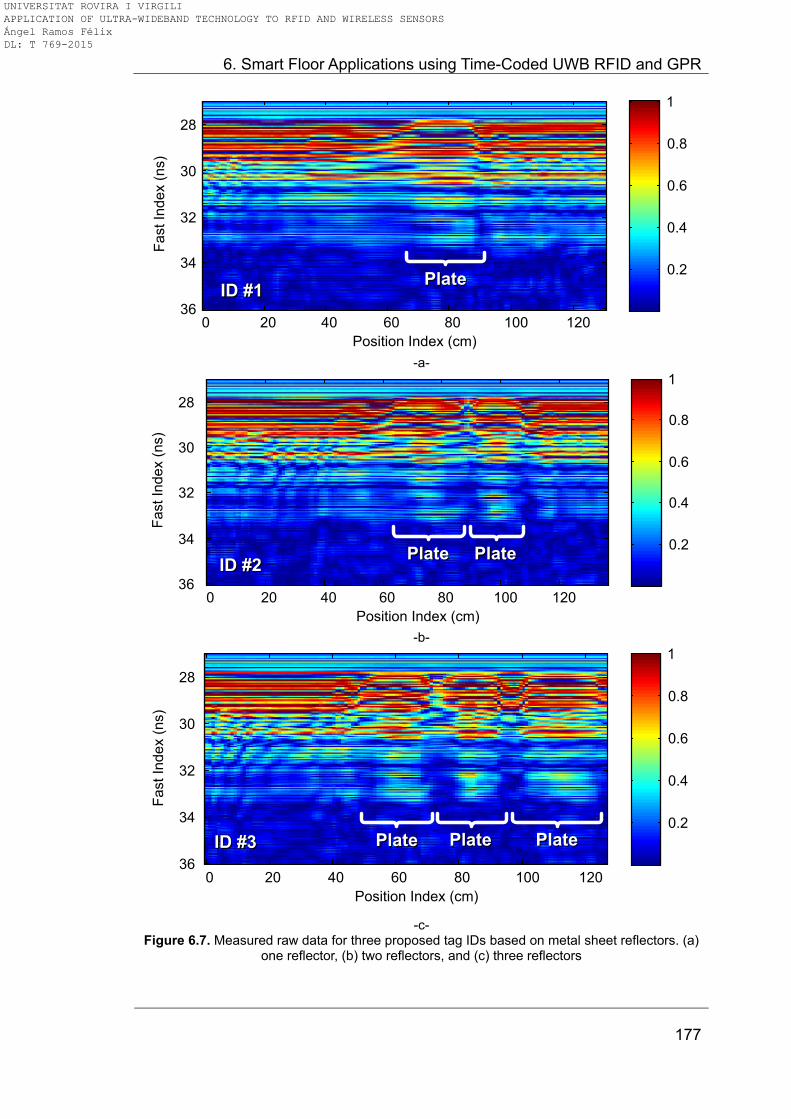
6. Smart Floor Applications using Time-Coded UWB RFID and GPR
177
Position Index (cm)
Fast In
dex (
ns)
0 20 40 60 80 100 120
28
30
32
34
36
0.2
0.4
0.6
0.8
1
PlatePlateID #1ID #1
-a-
Position Index (cm)
Fa
st In
de
x (
ns)
0 20 40 60 80 100 120
28
30
32
34
36
0.2
0.4
0.6
0.8
1
PlatePlateID #2ID #2
PlatePlate
-b-
Position Index (cm)
Fast In
dex (
ns)
0 20 40 60 80 100 120
28
30
32
34
36
0.2
0.4
0.6
0.8
1
PlatePlateID #3ID #3 PlatePlate PlatePlate
-c-
Figure 6.7. Measured raw data for three proposed tag IDs based on metal sheet reflectors. (a) one reflector, (b) two reflectors, and (c) three reflectors
UNIVERSITAT ROVIRA I VIRGILI APPLICATION OF ULTRA-WIDEBAND TECHNOLOGY TO RFID AND WIRELESS SENSORS Ángel Ramos Félix DL: T 769-2015

Application of Ultra-Wideband Technology to RFID and Wireless Sensors
178
Position Index (cm)
Fa
st In
de
x (
ns)
20 40 60 80 100 120 140
28
30
32
34
36
Position Index (cm)
20 40 60 80 100 120 1400
0.2
0.4
0.6
0.8
1Tag 1Tag 1 Tag 2Tag 2
Figure 6.8. Measured chipless UWB tags under the ceramic floor, for two tag IDs
20 25 30 35 40 45 500
0.2
0.4
0.6
0.8
1
Time (ns)
No
rma
lize
d A
mp
litu
de
Delay 1
Delay 2
Noise floor
Ceramic
Floor +
Structural
Mode
Ground
Floor
Tag
Modes
Figure 6.9. Cut at 59.34 cm of the measured chipless UWB tags under the ceramic floor, for
two tag IDs
Position Index (cm)
Fast In
dex (
ns)
20 40 60 80 100 120 140
28
30
32
34
36
0
0.2
0.4
0.6
0.8
1
Figure 6.10. Differential signal between the two chipless tag IDs
UNIVERSITAT ROVIRA I VIRGILI APPLICATION OF ULTRA-WIDEBAND TECHNOLOGY TO RFID AND WIRELESS SENSORS Ángel Ramos Félix DL: T 769-2015
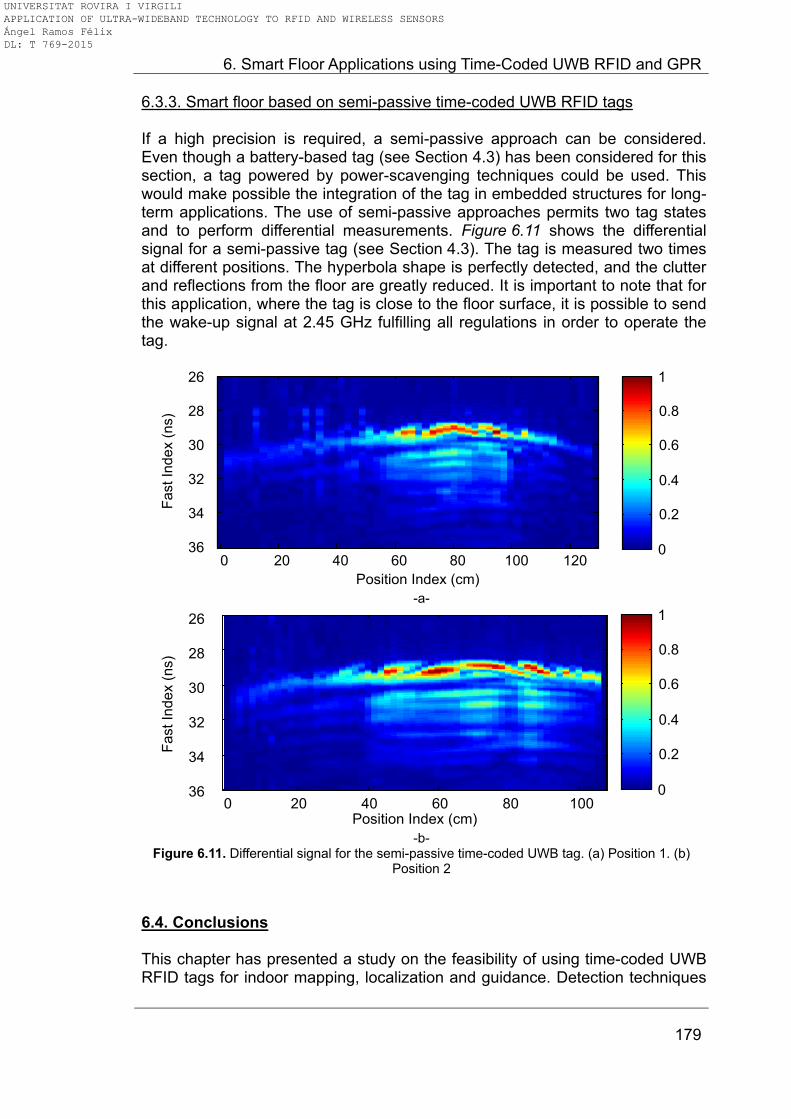
6. Smart Floor Applications using Time-Coded UWB RFID and GPR
179
6.3.3. Smart floor based on semi-passive time-coded UWB RFID tags If a high precision is required, a semi-passive approach can be considered. Even though a battery-based tag (see Section 4.3) has been considered for this section, a tag powered by power-scavenging techniques could be used. This would make possible the integration of the tag in embedded structures for long-term applications. The use of semi-passive approaches permits two tag states and to perform differential measurements. Figure 6.11 shows the differential signal for a semi-passive tag (see Section 4.3). The tag is measured two times at different positions. The hyperbola shape is perfectly detected, and the clutter and reflections from the floor are greatly reduced. It is important to note that for this application, where the tag is close to the floor surface, it is possible to send the wake-up signal at 2.45 GHz fulfilling all regulations in order to operate the tag.
Position Index (cm)
Fast In
dex (
ns)
0 20 40 60 80 100 120
26
28
30
32
34
36 0
0.2
0.4
0.6
0.8
1
-a-
Fast In
dex (
ns)
26
28
30
32
34
36 0
0.2
0.4
0.6
0.8
1
Position Index (cm)
0 20 40 60 80 100
-b-
Figure 6.11. Differential signal for the semi-passive time-coded UWB tag. (a) Position 1. (b) Position 2
6.4. Conclusions This chapter has presented a study on the feasibility of using time-coded UWB RFID tags for indoor mapping, localization and guidance. Detection techniques
UNIVERSITAT ROVIRA I VIRGILI APPLICATION OF ULTRA-WIDEBAND TECHNOLOGY TO RFID AND WIRELESS SENSORS Ángel Ramos Félix DL: T 769-2015
Application of Ultra-Wideband Technology to RFID and Wireless Sensors
180
based on ground penetrating radar (GPR) applications have been used and combined with time-coded UWB RFID tags. Detection of buried tags based on passive reflectors, chipless time-coded RFID and semi-passive time-coded RFID have been presented. The passive reflectors and the chipless time-coded UWB tags provide a low-cost and simple solution for smart floors for tracking and guidance. However, they are less robust to noise and they have a lower precision than semi-passive tags. Semi-passive tags are a more expensive and complex solution, but with a higher reliability and precision and the possibility to store information. 6.5. Bibliography [6.1] S. Han, H. Lim, and J. Lee. “An efficient localization scheme for a differential-driving
mobile robot based on RFID system,” IEEE Transactions on Industrial Electronics, Vol. 54, No. 6, pp. 3362-3369, 2007.
[6.2] M. Wong Siew, E. Tan Chong, and N. Huda bt Nik Zulkifli, “Efficient RFID tag
placement framework for in building navigation system for the blind,” 2010 8th Asia-Pacific Symposium on Information and Telecommunication Technologies (APSITT), 15-18 June 2010.
[6.3] A. R. Jimenez, F. Seco, J. C. Prieto, and J. I. Guevara, "Accurate Pedestrian Indoor
Navigation by Tightly Coupling Foot-Mounted IMU and RFID Measurements," IEEE Transactions on Instrumentation and Measurement, Vol. 61, No. 1, pp. 178-189, 2012.
[6.4] B. Olszewski, S. Fenton, B. Tworek, J. Liang, and K. Yelamarthi, “RFID positioning
robot: An indoor navigation system,” 2013 IEEE International Conference on Electro/Information Technology (EIT), 9-11 May 2013.
[6.5] J. Koch, J. Wettach, E. Bloch, and K. Berns, “Indoor Localisation of Humans, Objects,
and mobile Robots with RFID Infrastructure,” 7th International Conference on Hybrid Intelligent Systems, pp. 271-276, 17-19 Sept. 2007.
[6.6] S. Park and H. Lee, “Self-Recognition of Vehicle Position Using UHF Passive RFID
Tags,” IEEE Trans. on Industrial Electronics, Vol. 60, No. 1, pp.226-234, Jan. 2013.
[6.7] R. Gonalves, J. Reis, E. Santana, N. B. Carvalho, P. Pinho, and L. Roselli, “Smart floor:
Indoor navigation based on RFID,” 2013 IEEE Wireless Power Transfer (WPT), pp. 103-106, 15-16 May 2013.
[6.8] R. Tesoriero, R. Tebar, J. A. Gallud, M. D. Lozano, and V. M. R. Penichet, “Improving
location awareness in indoor spaces using RFID technology”, Expert Systems with Applications, Vol. 37, No. 1, pp. 894-898, 2010.
[6.9] D. J. Daniels, “Ground penetrating radar”, John Wiley & Sons, Inc., 2005.
[6.10] GPR Max, “GprMAX V2.0,” http://www.gprmax.com/, Nov. 2014 [Nov. 7, 2014].
[6.11] A. Lazaro, D. Girbau, and R. Villarino, “Techniques for Clutter Suppression in the Presence of Body Movements during the Detection of Respiratory Activity through UWB Radars,” Sensors 2014, pp. 2595-2618, 2014.
UNIVERSITAT ROVIRA I VIRGILI APPLICATION OF ULTRA-WIDEBAND TECHNOLOGY TO RFID AND WIRELESS SENSORS Ángel Ramos Félix DL: T 769-2015
7. Active Time-Coded UWB RFID
181
7. Active Time-Coded UWB RFID 7.1. Introduction The read range of about 8 meters achieved with the backscatterer semi-passive systems proposed in Chapter 4 might not be enough for long-range RFID-enabled localization applications. It is clearly noticeable that greater distances are required to cover a large indoor/outdoor area. This chapter proposes two active time-coded UWB RFID systems for localization applications. The goal is to increase the radar cross section (RCS) of the tag by providing it with gain. This has already been used in active reflectors proposed as active radar calibrators [7.1]. In the same direction, passive and active Van Atta Arrays have also been proposed for narrow band RFID applications [7.2-7.3]. Here, both proposed systems consist of an amplifier integrated in a time-coded UWB RFID tag which increases the power of the backscattered tag mode:
A system based on an amplifier and a UWB RFID tag in cross polarization
A system based on a reflection amplifier They will be presented and compared in terms of tag size, read range, cost and power consumption. This chapter is organized as follows:
Section 7.2 presents the active system based on amplifier in cross-polarization
Section 7.3 presents the active system based on a reflection amplifier
Finally, Section 7.4 compares both systems in terms of power consumption, bandwidth, read-range and tag size.
7.2. Active UWB RFID system based on cross-polarization amplifier Here, the tag consists of one receiver UWB antenna followed by a UWB amplifier connected through a delay-line to a transmitter UWB antenna. This tag is simpler than other active tags or reflectors [7.4-7.7], because it does not require complex synchronization techniques between the pulse generator included in the tag (here is no pulse generator, only the reader‟s pulse is amplified) and the receiver in the reader [7.7]. Several low-noise integrated amplifiers for UWB have been reported in the literature (a comparison is given in [7.8], Table III) and they can be integrated in the proposed tag. These amplifiers achieve power consumptions between 1.3 mW and 25 mW, depending on the CMOS process, topology and gain. The tag proposed here, therefore, needs no special integrated designs. In this section, a proof of concept prototype using commercial components is presented. In addition, since the read range is a key point in active tags, the link budget is also studied.
UNIVERSITAT ROVIRA I VIRGILI APPLICATION OF ULTRA-WIDEBAND TECHNOLOGY TO RFID AND WIRELESS SENSORS Ángel Ramos Félix DL: T 769-2015
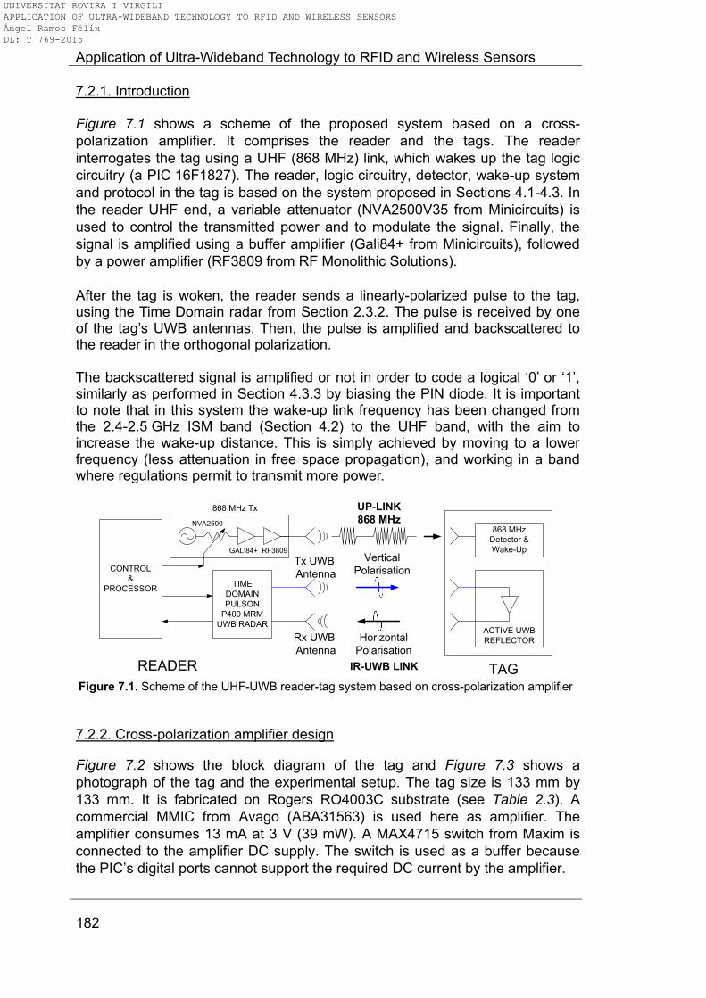
Application of Ultra-Wideband Technology to RFID and Wireless Sensors
182
7.2.1. Introduction Figure 7.1 shows a scheme of the proposed system based on a cross-
polarization amplifier. It comprises the reader and the tags. The reader
interrogates the tag using a UHF (868 MHz) link, which wakes up the tag logic
circuitry (a PIC 16F1827). The reader, logic circuitry, detector, wake-up system
and protocol in the tag is based on the system proposed in Sections 4.1-4.3. In
the reader UHF end, a variable attenuator (NVA2500V35 from Minicircuits) is
used to control the transmitted power and to modulate the signal. Finally, the
signal is amplified using a buffer amplifier (Gali84+ from Minicircuits), followed
by a power amplifier (RF3809 from RF Monolithic Solutions).
After the tag is woken, the reader sends a linearly-polarized pulse to the tag, using the Time Domain radar from Section 2.3.2. The pulse is received by one of the tag‟s UWB antennas. Then, the pulse is amplified and backscattered to the reader in the orthogonal polarization. The backscattered signal is amplified or not in order to code a logical „0‟ or „1‟, similarly as performed in Section 4.3.3 by biasing the PIN diode. It is important to note that in this system the wake-up link frequency has been changed from the 2.4-2.5 GHz ISM band (Section 4.2) to the UHF band, with the aim to increase the wake-up distance. This is simply achieved by moving to a lower frequency (less attenuation in free space propagation), and working in a band where regulations permit to transmit more power.
CONTROL
&
PROCESSORTIME
DOMAIN
PULSON
P400 MRM
UWB RADAR
868 MHz
Detector &
Wake-Up
UP-LINK
868 MHz
ACTIVE UWB
REFLECTOR
Tx UWB
Antenna
Rx UWB
Antenna
Vertical
Polarisation
Horizontal
Polarisation
TAGREADER IR-UWB LINK
868 MHz Tx
GALI84+ RF3809
NVA2500
Figure 7.1. Scheme of the UHF-UWB reader-tag system based on cross-polarization amplifier
7.2.2. Cross-polarization amplifier design
Figure 7.2 shows the block diagram of the tag and Figure 7.3 shows a
photograph of the tag and the experimental setup. The tag size is 133 mm by
133 mm. It is fabricated on Rogers RO4003C substrate (see Table 2.3). A
commercial MMIC from Avago (ABA31563) is used here as amplifier. The
amplifier consumes 13 mA at 3 V (39 mW). A MAX4715 switch from Maxim is
connected to the amplifier DC supply. The switch is used as a buffer because
the PIC‟s digital ports cannot support the required DC current by the amplifier.
UNIVERSITAT ROVIRA I VIRGILI APPLICATION OF ULTRA-WIDEBAND TECHNOLOGY TO RFID AND WIRELESS SENSORS Ángel Ramos Félix DL: T 769-2015
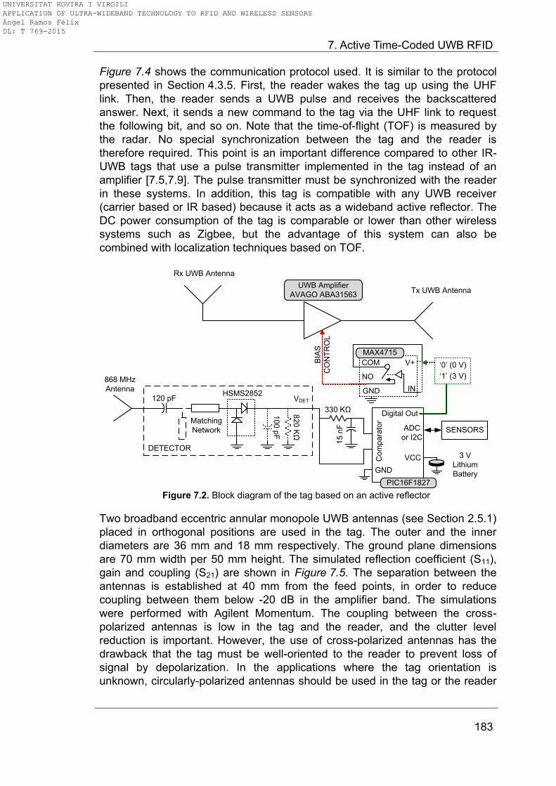
7. Active Time-Coded UWB RFID
183
Figure 7.4 shows the communication protocol used. It is similar to the protocol
presented in Section 4.3.5. First, the reader wakes the tag up using the UHF
link. Then, the reader sends a UWB pulse and receives the backscattered
answer. Next, it sends a new command to the tag via the UHF link to request
the following bit, and so on. Note that the time-of-flight (TOF) is measured by
the radar. No special synchronization between the tag and the reader is
therefore required. This point is an important difference compared to other IR-
UWB tags that use a pulse transmitter implemented in the tag instead of an
amplifier [7.5,7.9]. The pulse transmitter must be synchronized with the reader
in these systems. In addition, this tag is compatible with any UWB receiver
(carrier based or IR based) because it acts as a wideband active reflector. The
DC power consumption of the tag is comparable or lower than other wireless
systems such as Zigbee, but the advantage of this system can also be
combined with localization techniques based on TOF.
Rx UWB Antenna
Tx UWB Antenna
120 pFHSMS2852
868 MHz
Antenna
VDET
SENSORS
BIA
S
CO
NT
RO
L
DETECTOR
Matching
Network
330 KΩ10
0 p
F
82
0 K
Ω
COM
NO
GND
V+
IN
MAX4715
„0‟ (0 V)
„1‟ (3 V)
GND
VCC 3 V
Lithium
BatteryPIC16F1827
UWB Amplifier
AVAGO ABA31563
15
nF
Co
mp
ara
tor
ADC
or I2C
Digital Out
Figure 7.2. Block diagram of the tag based on an active reflector
Two broadband eccentric annular monopole UWB antennas (see Section 2.5.1)
placed in orthogonal positions are used in the tag. The outer and the inner
diameters are 36 mm and 18 mm respectively. The ground plane dimensions
are 70 mm width per 50 mm height. The simulated reflection coefficient (S11),
gain and coupling (S21) are shown in Figure 7.5. The separation between the
antennas is established at 40 mm from the feed points, in order to reduce
coupling between them below -20 dB in the amplifier band. The simulations
were performed with Agilent Momentum. The coupling between the cross-
polarized antennas is low in the tag and the reader, and the clutter level
reduction is important. However, the use of cross-polarized antennas has the
drawback that the tag must be well-oriented to the reader to prevent loss of
signal by depolarization. In the applications where the tag orientation is
unknown, circularly-polarized antennas should be used in the tag or the reader
UNIVERSITAT ROVIRA I VIRGILI APPLICATION OF ULTRA-WIDEBAND TECHNOLOGY TO RFID AND WIRELESS SENSORS Ángel Ramos Félix DL: T 769-2015

Application of Ultra-Wideband Technology to RFID and Wireless Sensors
184
end. Standard circularly-polarized patch antennas such as the ones used in
commercial UHF RFID applications [7.10] can be used for the UHF link.
Circularly-polarized UWB antennas such as the ones presented in Section 2.5.3
could be used in the UWB link.
UWB
Rx Antenna
UWB
Tx Antenna
Matching Network UHF Ant.
HSMS-2852
Diode
PIC
16F1827
Temperature
Sensor
MAX4715
Switch
Program.
pinouts
LC Notch
Filter
ABA31563
Amplifier
-a-
Control PC
Tag
UWB Tx
Antenna
UWB Rx
Antenna
UHF
Antenna
UHF
Generator
UWB Radar
-b-
Figure 7.3. Photograph of the implemented tag (a) and experimental setup (b)
In order to save space, a ceramic antenna (model P/N 0868AT43A0020 from Johanson Technology) was connected to the input of the UHF detector. The antenna has a peak gain of -1 dB in the 868 MHz band. A matching network composed of a 15 nH series inductor and 4.7 pF parallel capacitor was designed to match the antenna in the 865-868 MHz band. Figure 7.6 shows the measured S parameters of the MMIC ABA31563 for the bias point of 3 V, 13 mA. Figure 7.7 shows the open-loop gain computed from the cascade simulation of the amplifier and the antennas coupling. It can be seen that the open-loop gain is up to 20 dB larger around 2 GHz due to the high gain of the amplifier. If necessary, the separation between antennas could be increased to minimize coupling and therefore to avoid oscillation, but the tag
UNIVERSITAT ROVIRA I VIRGILI APPLICATION OF ULTRA-WIDEBAND TECHNOLOGY TO RFID AND WIRELESS SENSORS Ángel Ramos Félix DL: T 769-2015
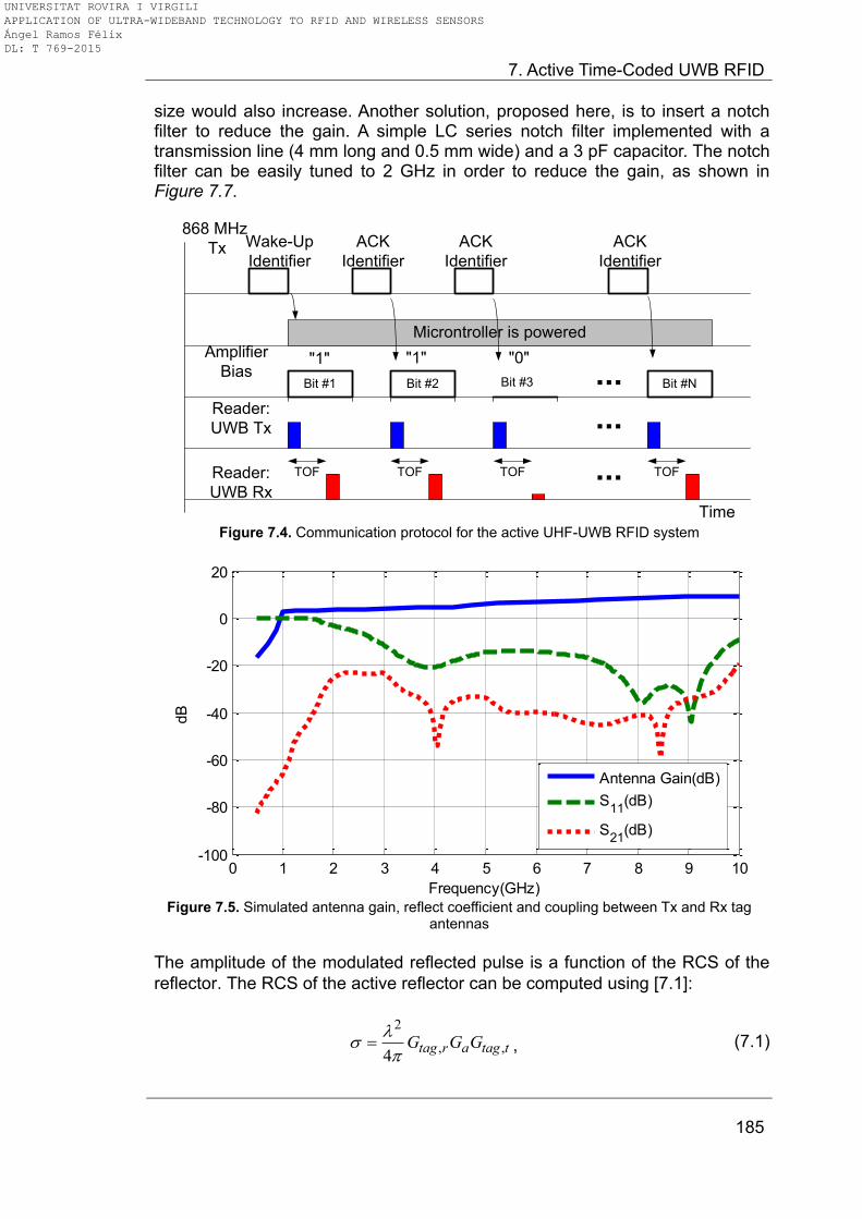
7. Active Time-Coded UWB RFID
185
size would also increase. Another solution, proposed here, is to insert a notch filter to reduce the gain. A simple LC series notch filter implemented with a transmission line (4 mm long and 0.5 mm wide) and a 3 pF capacitor. The notch filter can be easily tuned to 2 GHz in order to reduce the gain, as shown in Figure 7.7.
Wake-Up
Identifier
Microntroller is powered
Bit #1
Amplifier
Bias
Reader:
UWB Tx
868 MHz
Tx
TOF
ACK
Identifier
Bit #2
TOFReader:
UWB Rx
"1" "1"
..."0"
Bit #3 Bit #N
TOF
...
...
ACK
Identifier
ACK
Identifier
TOF
Time Figure 7.4. Communication protocol for the active UHF-UWB RFID system
Figure 7.5. Simulated antenna gain, reflect coefficient and coupling between Tx and Rx tag
antennas
The amplitude of the modulated reflected pulse is a function of the RCS of the
reflector. The RCS of the active reflector can be computed using [7.1]:
2
, ,4
tag r a tag tG G G
, (7.1)
0 1 2 3 4 5 6 7 8 9 10-100
-80
-60
-40
-20
0
20
Frequency(GHz)
dB
Antenna Gain(dB)
S11
(dB)
S21
(dB)
UNIVERSITAT ROVIRA I VIRGILI APPLICATION OF ULTRA-WIDEBAND TECHNOLOGY TO RFID AND WIRELESS SENSORS Ángel Ramos Félix DL: T 769-2015
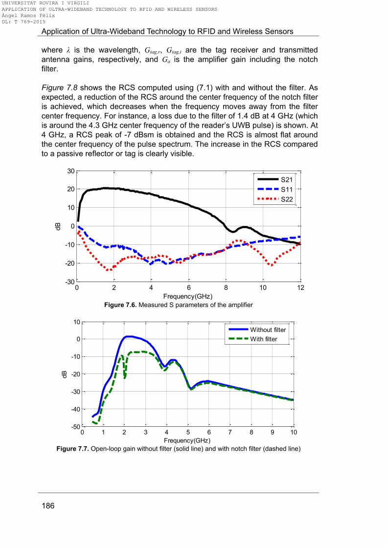
Application of Ultra-Wideband Technology to RFID and Wireless Sensors
186
where λ is the wavelength, Gtag,r, Gtag,t are the tag receiver and transmitted
antenna gains, respectively, and Ga is the amplifier gain including the notch
filter.
Figure 7.8 shows the RCS computed using (7.1) with and without the filter. As
expected, a reduction of the RCS around the center frequency of the notch filter
is achieved, which decreases when the frequency moves away from the filter
center frequency. For instance, a loss due to the filter of 1.4 dB at 4 GHz (which
is around the 4.3 GHz center frequency of the reader‟s UWB pulse) is shown. At
4 GHz, a RCS peak of -7 dBsm is obtained and the RCS is almost flat around
the center frequency of the pulse spectrum. The increase in the RCS compared
to a passive reflector or tag is clearly visible.
Figure 7.6. Measured S parameters of the amplifier
Figure 7.7. Open-loop gain without filter (solid line) and with notch filter (dashed line)
0 2 4 6 8 10 12-30
-20
-10
0
10
20
30
Frequency(GHz)
dB
S21
S11
S22
0 1 2 3 4 5 6 7 8 9 10-50
-40
-30
-20
-10
0
10
Frequency(GHz)
dB
Without filter
With filter
UNIVERSITAT ROVIRA I VIRGILI APPLICATION OF ULTRA-WIDEBAND TECHNOLOGY TO RFID AND WIRELESS SENSORS Ángel Ramos Félix DL: T 769-2015
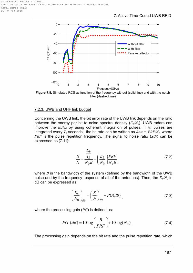
7. Active Time-Coded UWB RFID
187
Figure 7.8. Simulated RCS as function of the frequency without (solid line) and with the notch
filter (dashed line)
7.2.3. UWB and UHF link budget Concerning the UWB link, the bit error rate of the UWB link depends on the ratio between the energy per bit to noise spectral density (Eb/N0). UWB radars can improve the Eb/N0 by using coherent integration of pulses. If Ns pulses are integrated every Tb seconds, the bit rate can be written as Rate = PRF/Ns, where PRF is the pulse repetition frequency. The signal to noise ratio (S/N) can be expressed as [7.11]:
0 0
b
b b
s
E
T ES PRF
N N B N N B
,
(7.2)
where B is the bandwidth of the system (defined by the bandwidth of the UWB pulse and by the frequency response of all of the antennas). Then, the Eb/N0 in dB can be expressed as:
0
( )b
dBdB
E SPG dB
N N
, (7.3)
where the processing gain (PG) is defined as:
( ) 10log 10log( )sB
PG dB NPRF
. (7.4)
The processing gain depends on the bit rate and the pulse repetition rate, which
0 1 2 3 4 5 6 7 8 9 10-120
-100
-80
-60
-40
-20
0
Frequency(GHz)
RC
S(d
Bsm
) Without filter
With filter
Passive reflector
UNIVERSITAT ROVIRA I VIRGILI APPLICATION OF ULTRA-WIDEBAND TECHNOLOGY TO RFID AND WIRELESS SENSORS Ángel Ramos Félix DL: T 769-2015
Application of Ultra-Wideband Technology to RFID and Wireless Sensors
188
are parameters that depend on the target application. The noise spectral density N0 is a function of the noise factor; according to the specification from the radar manufacturer, it is 4.8 dB [7.12]. An F = 5.8 dB has been chosen, adding 1 dB to take into account the cables between the radar and the antennas.
0 0N kT F , (7.5)
and the average receiver power can be obtained from the radar equation:
2
2 2
1
44 4
tt r
PS G G
r r
, (7.6)
where the RCS (σ) of the active reflector is given by (7.1), r is the tag-to-reader distance, Pt is the transmitted power, Gt and Gr are the gains of the Tx and Rx antennas, and λ is the wavelength. Figure 7.9 shows the Eb/N0 calculated with the equations above. For the simulations, an amplifier with a gain of 16 dB, bandwidth B = 1.35 GHz [7.12], two UWB tag antennas with a gain of 5 dB and two UWB reader antennas with a gain of 6 dB were considered. The calculation was performed at the radar center frequency (4.3 GHz, see Section 2.3.2) of the pulse and a 1.35 GHz bandwidth was taken into account. The average equivalent radiated power used is -14.5 dBm (FCC 15b compliant) and the PRF is 10.1 MHz. Assuming a BER limit of 10-3, an Eb/N0 of 6.8 dB is required for Binary Phase Shift Keying (BPSK) demodulation. From this simulation, depending on the number of samples Ns (1, 64, 4096 or 32768 can be used with the P400 radar), read ranges of 3.6 m, 9.5 m, 27.5 m and 45.5 m can be theoretically achieved, respectively. In order to show the worst case, Figure 7.10 shows the Eb/N0 calculated assuming the tag antenna gain equal to 0 dBi. A comparison with the case of a passive tag (Ga = 1) [7.13] is also included. In this case, the active approach indicates a read range of about 25 m compared with 12 m of the passive approach. Concerning the UHF link, Figure 7.11 shows the measured voltage at the output of the detector as a function of the input power. The tangential sensitivity (TSS) is the lowest input power for which the detector will have an 8 dB signal-to-noise ratio at the output of a test video amplifier. A tangential sensitivity value of -57 dBm is typically obtained using zero bias diodes [7.14]. Setting the sensitivity of the wake-up system to -40 dBm (3 mV of detected voltage) would therefore be enough to ensure a good link quality. Figure 7.12 shows the received input power at the detector as a function of the distance. To avoid the uplink limiting the read range, the minimum wake-up distance should be larger than 45.5 m in free space, which is the theoretical simulated limit for the UWB link obtained above. As explained in Section 4.2.2, a detector at the 2.4-2.5 GHz ISM band cannot achieve this distance considering power regulations. The UHF band was chosen for this reason. Using the maximum power transmitted under European (ETSI EN 302 208) and USA (FCC-15) RFID regulations, a theoretical distance longer than 70 m can be obtained in free space. A wake-up antenna gain of -
UNIVERSITAT ROVIRA I VIRGILI APPLICATION OF ULTRA-WIDEBAND TECHNOLOGY TO RFID AND WIRELESS SENSORS Ángel Ramos Félix DL: T 769-2015
7. Active Time-Coded UWB RFID
189
1 dB was considered in the calculations. Since the wake-up distances are much larger than the maximum read range (limited by the UWB link), there is consequently a fading margin to mitigate multipath effects in the UHF channel. The data rate is limited by the low-pass filter at the output of the detector and by the speed of the internal comparator in the microcontroller. In the experiments the data rate used is 1 KHz. However, it can be increased up to 40 KHz (see Section 4.3.2). These speeds are high enough to send small configuration commands if sensors are integrated in this tag.
Figure 7.9. Simulated Eb/N0 as a function of the distance for different integration sampling
numbers (Ns = 1, 64, 4096, and 32768). The limit line for BER = 10-3
(Eb/N0 = 6.8 dB) is also indicated
Figure 7.10. Simulated Eb/N0 as a function of the distance for an active reflector (solid line) and
a passive reflector (dashed line). The tag antenna gain is assumed 0 dBi and the integration sampling number Ns = 32768. The limit line for BER = 10
-3 (Eb/N0 = 6.8 dB) is also indicated
0 5 10 15 20 25 30 35 40 45 50-40
-20
0
20
40
60
80
100
120
Distance(m)
Eb/N
0(d
B)
Ns=1
Ns=64
Ns=4096
Ns=32768
BER=10-3
0 5 10 15 20 25 30 35 40 45 50-50
0
50
100
150
Distance(m)
Eb/N
0(d
B)
Active Ns=32768
Passive Ns=32768
BER=10-3
UNIVERSITAT ROVIRA I VIRGILI APPLICATION OF ULTRA-WIDEBAND TECHNOLOGY TO RFID AND WIRELESS SENSORS Ángel Ramos Félix DL: T 769-2015
Application of Ultra-Wideband Technology to RFID and Wireless Sensors
190
Figure 7.11. Measured detected voltage as a function of the input power at 868 MHz
Figure 7.12. Received power as a function of the tag to reader distance for the uplink
7.2.4. Results Figures 7.13-7.14 show the UWB signal received after background subtraction is applied as a function of the delay for a tag located 1 m and 10 m away from the reader, respectively, in an indoor scenario. A small reflection due to the tag structure is observed when the amplifier is biased OFF (State OFF). In contrast, there is a strong reflection when the amplifier is biased ON (State ON). A small delay is observed between the two states due to the propagation delay through
-70 -60 -50 -40 -30 -20 -10 0 10 2010
-5
10-4
10-3
10-2
10-1
100
101
Input Power (dBm)
Voltage (
V)
0 10 20 30 40 50 60 70 80 90 100-80
-60
-40
-20
0
20
40
Distance(m)
Receiv
ed P
ow
er
(dB
m)
2.45 GHz ISM Band
EU RFID Band
USA RFID Band
Sensitivity
UNIVERSITAT ROVIRA I VIRGILI APPLICATION OF ULTRA-WIDEBAND TECHNOLOGY TO RFID AND WIRELESS SENSORS Ángel Ramos Félix DL: T 769-2015
7. Active Time-Coded UWB RFID
191
the amplifier. Multiple reflections are also observed for the State ON due to feedback coupling between the tag antennas.
Figure 7.13. Normalized received UWB raw signal as a function of time delay for the two
states (amplifier ON and OFF) at a tag-to-reader distance of 1 m
Figures 7.15-7.16 show the normalized magnitude of the CWT (see Section 2.4.2) applied to the received signal at 1 m and 10 m, respectively. In both cases, the received signal in State ON is clearly detectable for both distances. For the State OFF, the tag is not retransmitting the reader‟s pulse. The signal received therefore consists of background and residual clutter. Next, the diferential coding scheme from Section 4.3.4 is applied. Figures 7.17-7.19 show the maximum magnitude of the CWT applied to the received signal after subtracting the received signal for the first bit. An arbitrary bit sequence (0101011) is transmitted which could correspond to a sensor data connected to the microcontroller, or an identifier code. In order to verify the simulations of Section 7.2.3, a measurement in an outdoor environment has been performed at a 45 m tag-reader distance. The result for the same sequence is shown in Figure 7.19. The effect of noise and clutter is clearly visible; however the bit sequence can be demodulated. The time delay of the peak for the ON states depends on the time-of-flight delay between the tag and the reader, added to a small systematic delay between the reader and its own antennas. This small delay due to the reader‟s antennas is known and is always the same for any tag-to-reader distance. This active reflector could thus be combined with time-of-arrival localization techniques by using multiple readers located at different known positions (anchors).
25 30 35 40 45 50 55-1
-0.5
0
0.5
1
Delay(ns)
Raw
sig
nal
State ON
25 30 35 40 45 50 55-1
-0.5
0
0.5
1
Delay(ns)
Raw
sig
nal
State OFF
UNIVERSITAT ROVIRA I VIRGILI APPLICATION OF ULTRA-WIDEBAND TECHNOLOGY TO RFID AND WIRELESS SENSORS Ángel Ramos Félix DL: T 769-2015
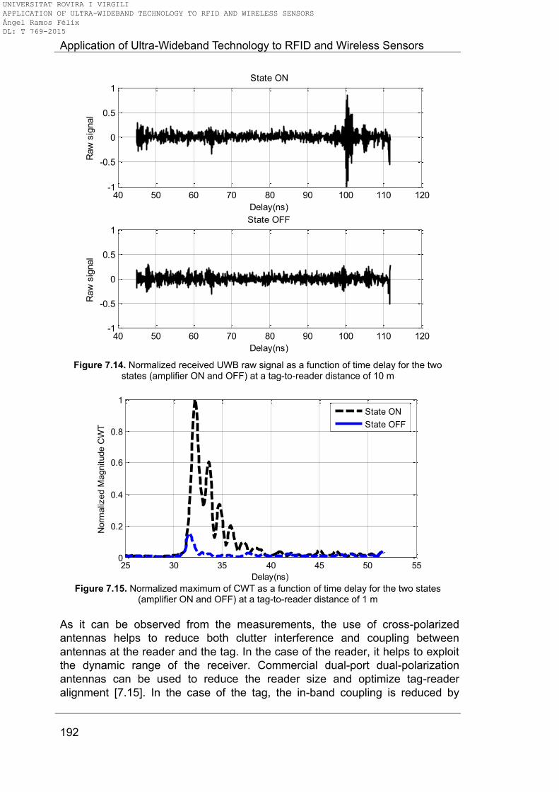
Application of Ultra-Wideband Technology to RFID and Wireless Sensors
192
Figure 7.14. Normalized received UWB raw signal as a function of time delay for the two
states (amplifier ON and OFF) at a tag-to-reader distance of 10 m
Figure 7.15. Normalized maximum of CWT as a function of time delay for the two states
(amplifier ON and OFF) at a tag-to-reader distance of 1 m
As it can be observed from the measurements, the use of cross-polarized
antennas helps to reduce both clutter interference and coupling between
antennas at the reader and the tag. In the case of the reader, it helps to exploit
the dynamic range of the receiver. Commercial dual-port dual-polarization
antennas can be used to reduce the reader size and optimize tag-reader
alignment [7.15]. In the case of the tag, the in-band coupling is reduced by
40 50 60 70 80 90 100 110 120-1
-0.5
0
0.5
1
Delay(ns)
Raw
sig
nal
State ON
40 50 60 70 80 90 100 110 120-1
-0.5
0
0.5
1
Delay(ns)
Raw
sig
nal
State OFF
25 30 35 40 45 50 550
0.2
0.4
0.6
0.8
1
Delay(ns)
Norm
aliz
ed M
agnitude C
WT
State ON
State OFF
UNIVERSITAT ROVIRA I VIRGILI APPLICATION OF ULTRA-WIDEBAND TECHNOLOGY TO RFID AND WIRELESS SENSORS Ángel Ramos Félix DL: T 769-2015
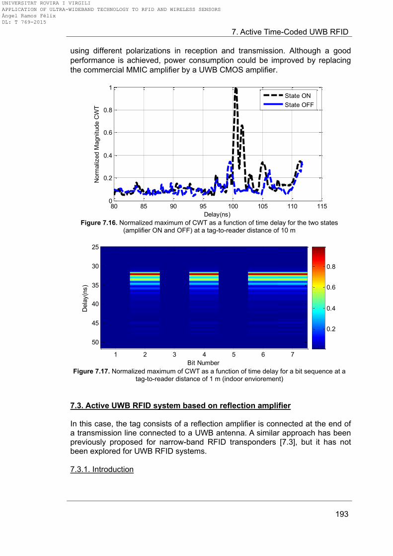
7. Active Time-Coded UWB RFID
193
using different polarizations in reception and transmission. Although a good
performance is achieved, power consumption could be improved by replacing
the commercial MMIC amplifier by a UWB CMOS amplifier.
Figure 7.16. Normalized maximum of CWT as a function of time delay for the two states
(amplifier ON and OFF) at a tag-to-reader distance of 10 m
Figure 7.17. Normalized maximum of CWT as a function of time delay for a bit sequence at a
tag-to-reader distance of 1 m (indoor enviorement)
7.3. Active UWB RFID system based on reflection amplifier In this case, the tag consists of a reflection amplifier is connected at the end of a transmission line connected to a UWB antenna. A similar approach has been previously proposed for narrow-band RFID transponders [7.3], but it has not been explored for UWB RFID systems. 7.3.1. Introduction
80 85 90 95 100 105 110 1150
0.2
0.4
0.6
0.8
1
Delay(ns)
Norm
aliz
ed M
agnitude C
WT
State ON
State OFF
Bit Number
Dela
y(n
s)
Bit sequence: 0 1 0 1 0 1 1
1 2 3 4 5 6 7
25
30
35
40
45
50
0.2
0.4
0.6
0.8
UNIVERSITAT ROVIRA I VIRGILI APPLICATION OF ULTRA-WIDEBAND TECHNOLOGY TO RFID AND WIRELESS SENSORS Ángel Ramos Félix DL: T 769-2015
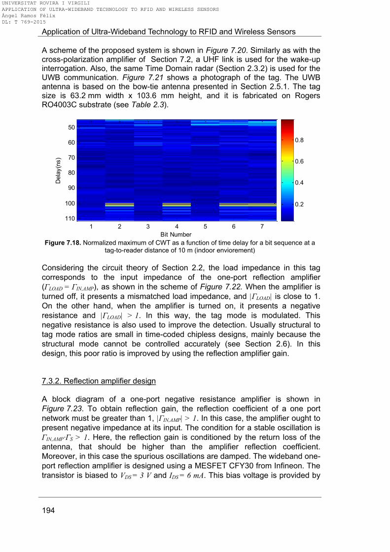
Application of Ultra-Wideband Technology to RFID and Wireless Sensors
194
A scheme of the proposed system is shown in Figure 7.20. Similarly as with the cross-polarization amplifier of Section 7.2, a UHF link is used for the wake-up interrogation. Also, the same Time Domain radar (Section 2.3.2) is used for the UWB communication. Figure 7.21 shows a photograph of the tag. The UWB antenna is based on the bow-tie antenna presented in Section 2.5.1. The tag size is 63.2 mm width x 103.6 mm height, and it is fabricated on Rogers RO4003C substrate (see Table 2.3).
Figure 7.18. Normalized maximum of CWT as a function of time delay for a bit sequence at a
tag-to-reader distance of 10 m (indoor enviorement)
Considering the circuit theory of Section 2.2, the load impedance in this tag
corresponds to the input impedance of the one-port reflection amplifier
(ΓLOAD = ΓIN,AMP), as shown in the scheme of Figure 7.22. When the amplifier is
turned off, it presents a mismatched load impedance, and |ΓLOAD| is close to 1.
On the other hand, when the amplifier is turned on, it presents a negative
resistance and |ΓLOAD| > 1. In this way, the tag mode is modulated. This
negative resistance is also used to improve the detection. Usually structural to
tag mode ratios are small in time-coded chipless designs, mainly because the
structural mode cannot be controlled accurately (see Section 2.6). In this
design, this poor ratio is improved by using the reflection amplifier gain.
7.3.2. Reflection amplifier design A block diagram of a one-port negative resistance amplifier is shown in
Figure 7.23. To obtain reflection gain, the reflection coefficient of a one port
network must be greater than 1, |ΓIN,AMP| > 1. In this case, the amplifier ought to
present negative impedance at its input. The condition for a stable oscillation is
ΓIN,AMP·ΓS > 1. Here, the reflection gain is conditioned by the return loss of the
antenna, that should be higher than the amplifier reflection coefficient.
Moreover, in this case the spurious oscillations are damped. The wideband one-
port reflection amplifier is designed using a MESFET CFY30 from Infineon. The
transistor is biased to VDS = 3 V and IDS = 6 mA. This bias voltage is provided by
Bit Number
Dela
y(n
s)
Bit sequence: 0 1 0 1 0 1 1
1 2 3 4 5 6 7
50
60
70
80
90
100
110
0.2
0.4
0.6
0.8
UNIVERSITAT ROVIRA I VIRGILI APPLICATION OF ULTRA-WIDEBAND TECHNOLOGY TO RFID AND WIRELESS SENSORS Ángel Ramos Félix DL: T 769-2015
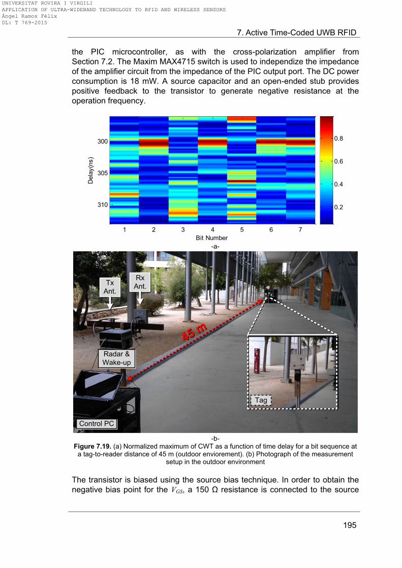
7. Active Time-Coded UWB RFID
195
the PIC microcontroller, as with the cross-polarization amplifier from
Section 7.2. The Maxim MAX4715 switch is used to independize the impedance
of the amplifier circuit from the impedance of the PIC output port. The DC power
consumption is 18 mW. A source capacitor and an open-ended stub provides
positive feedback to the transistor to generate negative resistance at the
operation frequency.
-a-
Tag
45 m45 m
Tx
Ant.
Rx
Ant.
Control PC
Radar &
Wake-up
-b-
Figure 7.19. (a) Normalized maximum of CWT as a function of time delay for a bit sequence at a tag-to-reader distance of 45 m (outdoor enviorement). (b) Photograph of the measurement
setup in the outdoor environment
The transistor is biased using the source bias technique. In order to obtain the
negative bias point for the VGS, a 150 Ω resistance is connected to the source
Bit Number
Dela
y(n
s)
Bit sequence: 0 1 0 1 0 1 1
1 2 3 4 5 6 7
300
305
310 0.2
0.4
0.6
0.8
UNIVERSITAT ROVIRA I VIRGILI APPLICATION OF ULTRA-WIDEBAND TECHNOLOGY TO RFID AND WIRELESS SENSORS Ángel Ramos Félix DL: T 769-2015
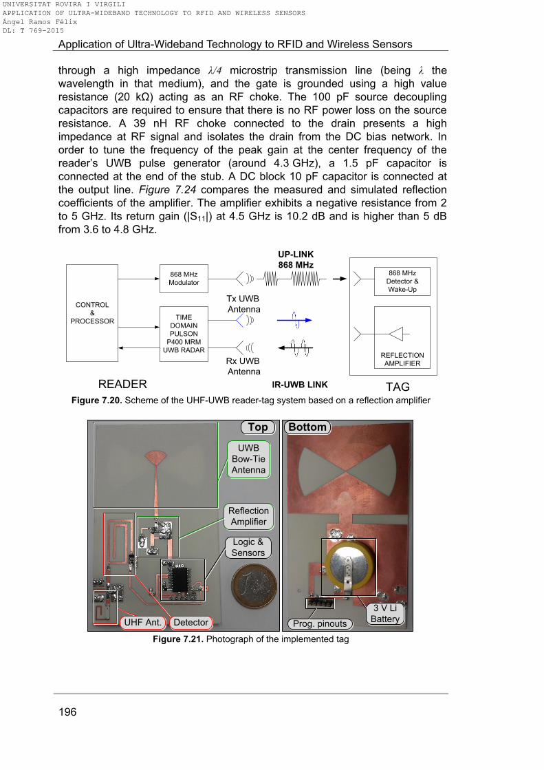
Application of Ultra-Wideband Technology to RFID and Wireless Sensors
196
through a high impedance λ/4 microstrip transmission line (being λ the
wavelength in that medium), and the gate is grounded using a high value
resistance (20 kΩ) acting as an RF choke. The 100 pF source decoupling
capacitors are required to ensure that there is no RF power loss on the source
resistance. A 39 nH RF choke connected to the drain presents a high
impedance at RF signal and isolates the drain from the DC bias network. In
order to tune the frequency of the peak gain at the center frequency of the
reader‟s UWB pulse generator (around 4.3 GHz), a 1.5 pF capacitor is
connected at the end of the stub. A DC block 10 pF capacitor is connected at
the output line. Figure 7.24 compares the measured and simulated reflection
coefficients of the amplifier. The amplifier exhibits a negative resistance from 2
to 5 GHz. Its return gain (|S11|) at 4.5 GHz is 10.2 dB and is higher than 5 dB
from 3.6 to 4.8 GHz.
Figure 7.20. Scheme of the UHF-UWB reader-tag system based on a reflection amplifier
UHF Ant.
UWB
Bow-Tie
Antenna
Logic &
Sensors
Detector
Reflection
Amplifier
3 V Li
BatteryProg. pinouts
Top Bottom
Figure 7.21. Photograph of the implemented tag
CONTROL
&
PROCESSORTIME
DOMAIN
PULSON
P400 MRM
UWB RADAR
868 MHz
Detector &
Wake-Up
UP-LINK
868 MHz
REFLECTION
AMPLIFIER
Tx UWB
Antenna
Rx UWB
Antenna
TAGREADER IR-UWB LINK
868 MHz
Modulator
UNIVERSITAT ROVIRA I VIRGILI APPLICATION OF ULTRA-WIDEBAND TECHNOLOGY TO RFID AND WIRELESS SENSORS Ángel Ramos Félix DL: T 769-2015
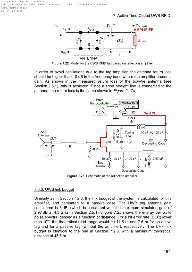
7. Active Time-Coded UWB RFID
197
S1
1a
S2
2a
S21a
S12a
L
ain
bout
ANTENNA
ZLOAD(Zc)
L
IN
AMPLIFIERS IN , AMP
Figure 7.22. Model for the UWB RFID tag based on reflection amplifier
In order to avoid oscillations due to the tag amplifier, the antenna return loss
should be higher than 10 dB in the frequency band where the amplifier presents
gain. As shown in the measured return loss of the bow-tie antenna (see
Section 2.5.1), this is achieved. Since a short straight line is connected to the
antenna, the return loss is the same shown in Figure 2.17a.
10 pF
0.47 pF100 pF150
20 k10 pF
1.5 pFCFY30Decoupling Caps
W=
0.5
mm
L=
8 m
m
W=
0.5
mm
L=
8 m
m
100 pF
100 pF
Decoupling Caps
VD (3 V)VD (3 V)
Tuning
StubOUT
UWB
Antenna
LS
Bias
Resistor
39 nH
COM
NO
GND
V+
IN
MAX4715
„0‟ (0 V)
„1‟ (3 V)
From
Microcontroller
From
Microcontroller
Figure 7.23. Schematic of the reflection amplifier
7.3.3. UWB link budget Similarly as in Section 7.2.3, the link budget of the system is calculated for this
amplifier, and compared to a passive case. The UWB tag antenna gain
considered is 3 dB, (which is consistent with the maximum simulated gain of
2.97 dB at 4.3 GHz in Section 2.5.1). Figure 7.25 shows the energy per bit to
noise spectral density as a function of distance. For a bit error rate (BER) lower
than 10-4, the theoretical read range would be 11.5 m and 7.6 m for an active
tag and for a passive tag (without the amplifier), respectively. The UHF link
budget is identical to the one in Section 7.2.3, with a maximum theoretical
distance of 45.5 m.
UNIVERSITAT ROVIRA I VIRGILI APPLICATION OF ULTRA-WIDEBAND TECHNOLOGY TO RFID AND WIRELESS SENSORS Ángel Ramos Félix DL: T 769-2015
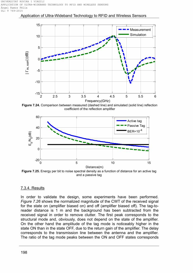
Application of Ultra-Wideband Technology to RFID and Wireless Sensors
198
|
IN,
AM
P| (
dB
)
Figure 7.24. Comparison between measured (dashed line) and simulated (solid line) reflection
coefficient of the reflection amplifier
Figure 7.25. Energy per bit to noise spectral density as a function of distance for an active tag
and a passive tag
7.3.4. Results In order to validate the design, some experiments have been performed. Figure 7.26 shows the normalized magnitude of the CWT of the received signal for the state on (amplifier biased on) and off (amplifier biased off). The tag-to-reader distance is 1 m and the background has been subtracted from the received signal in order to remove clutter. The first peak corresponds to the structural mode and, obviously, does not depend on the state of the amplifier. On the other hand the amplitude of the tag mode is noticeably higher in the state ON than in the state OFF, due to the return gain of the amplifier. The delay corresponds to the transmission line between the antenna and the amplifier. The ratio of the tag mode peaks between the ON and OFF states corresponds
2 2.5 3 3.5 4 4.5 5 5.5 6-15
-10
-5
0
5
10
15
Frequency(GHz)
S11(d
B)
Measurement
Simulation
0 5 10 15-20
0
20
40
60
Distance(m)
Eb/N
0(d
B)
Active tag
Passive Tag
BER=10-4
UNIVERSITAT ROVIRA I VIRGILI APPLICATION OF ULTRA-WIDEBAND TECHNOLOGY TO RFID AND WIRELESS SENSORS Ángel Ramos Félix DL: T 769-2015
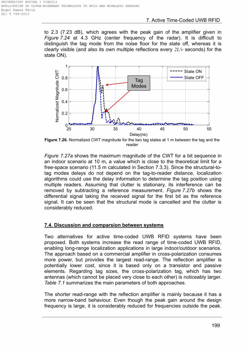
7. Active Time-Coded UWB RFID
199
to 2.3 (7.23 dB), which agrees with the peak gain of the amplifier given in Figure 7.24 at 4.3 GHz (center frequency of the radar). It is difficult to distinguish the tag mode from the noise floor for the state off, whereas it is clearly visible (and also its own multiple reflections every 2L/v seconds) for the state ON).
Figure 7.26. Normalized CWT magnitude for the two tag states at 1 m between the tag and the
reader
Figure 7.27a shows the maximum magnitude of the CWT for a bit sequence in an indoor scenario at 10 m, a value which is close to the theoretical limit for a free-space scenario (11.5 m calculated in Section 7.3.3). Since the structural-to-tag modes delays do not depend on the tag-to-reader distance, localization algorithms could use the delay information to determine the tag position using multiple readers. Assuming that clutter is stationary, its interference can be removed by subtracting a reference measurement. Figure 7.27b shows the differential signal taking the received signal for the first bit as the reference signal. It can be seen that the structural mode is cancelled and the clutter is considerably reduced. 7.4. Discussion and comparsion between systems Two alternatives for active time-coded UWB RFID systems have been proposed. Both systems increase the read range of time-coded UWB RFID, enabling long-range localization applications in large indoor/outdoor scenarios. The approach based on a commercial amplifier in cross-polarization consumes more power, but provides the largest read-range. The reflection amplifier is potentially lower cost, since it is based only on a transistor and passive elements. Regarding tag sizes, the cross-polarization tag, which has two antennas (which cannot be placed very close to each other) is noticeably larger. Table 7.1 summarizes the main parameters of both approaches. The shorter read-range with the reflection amplifier is mainly because it has a more narrow-band behaviour. Even though the peak gain around the design frequency is large, it is considerably reduced for frequencies outside the peak.
25 30 35 40 45 50 550
0.2
0.4
0.6
0.8
1
Delay(ns)
Norm
aliz
ed M
agnitude C
WT State ON
State OFFTag
Modes
UNIVERSITAT ROVIRA I VIRGILI APPLICATION OF ULTRA-WIDEBAND TECHNOLOGY TO RFID AND WIRELESS SENSORS Ángel Ramos Félix DL: T 769-2015
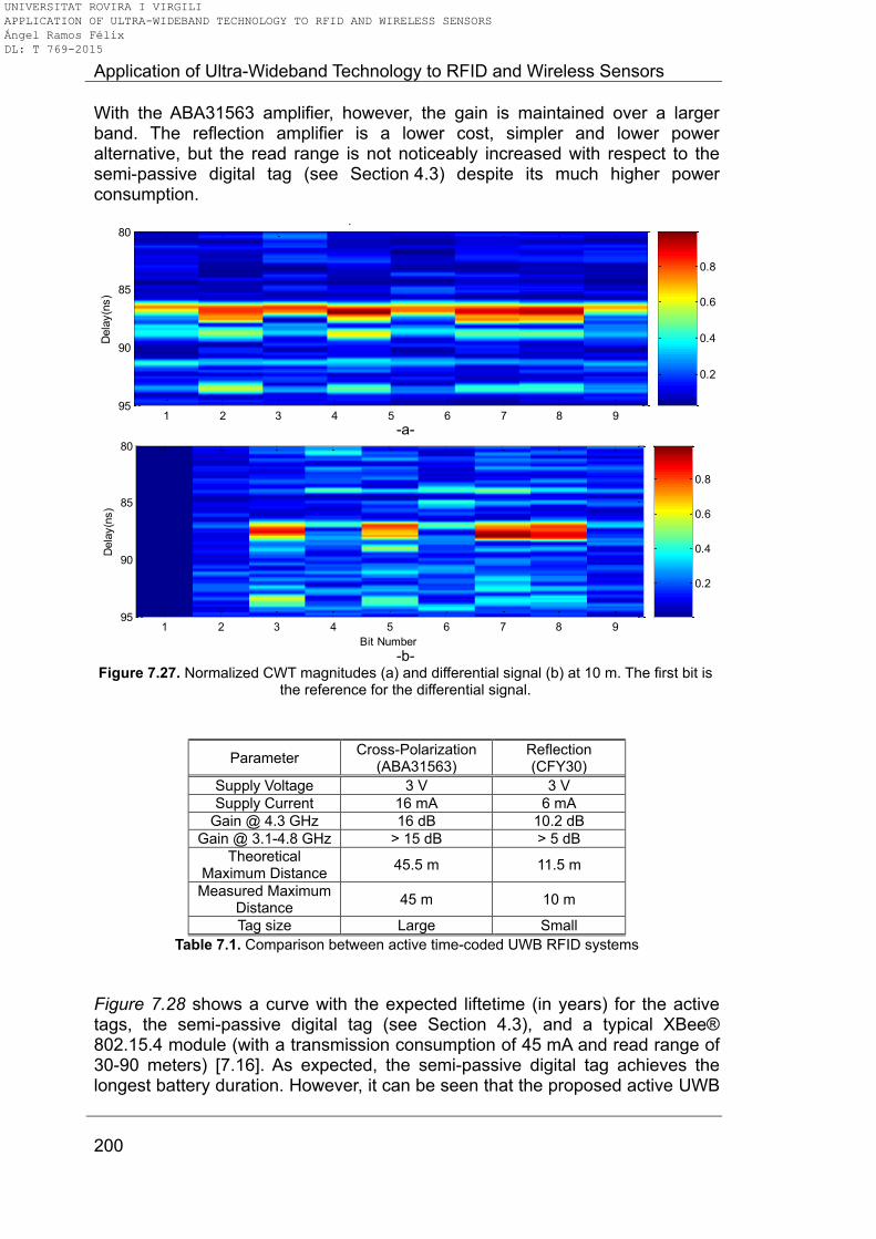
Application of Ultra-Wideband Technology to RFID and Wireless Sensors
200
With the ABA31563 amplifier, however, the gain is maintained over a larger band. The reflection amplifier is a lower cost, simpler and lower power alternative, but the read range is not noticeably increased with respect to the semi-passive digital tag (see Section 4.3) despite its much higher power consumption.
-a-
-b-
Figure 7.27. Normalized CWT magnitudes (a) and differential signal (b) at 10 m. The first bit is the reference for the differential signal.
Parameter Cross-Polarization
(ABA31563) Reflection (CFY30)
Supply Voltage 3 V 3 V
Supply Current 16 mA 6 mA
Gain @ 4.3 GHz 16 dB 10.2 dB
Gain @ 3.1-4.8 GHz > 15 dB > 5 dB
Theoretical Maximum Distance
45.5 m 11.5 m
Measured Maximum Distance
45 m 10 m
Tag size Large Small
Table 7.1. Comparison between active time-coded UWB RFID systems
Figure 7.28 shows a curve with the expected liftetime (in years) for the active tags, the semi-passive digital tag (see Section 4.3), and a typical XBee® 802.15.4 module (with a transmission consumption of 45 mA and read range of 30-90 meters) [7.16]. As expected, the semi-passive digital tag achieves the longest battery duration. However, it can be seen that the proposed active UWB
Dela
y(n
s)
Bit sequence: 0 0 1 0 1 0 1 1
1 2 3 4 5 6 7 8 9
80
85
90
95
0.2
0.4
0.6
0.8
Bit Number
Dela
y(n
s)
1 2 3 4 5 6 7 8 9
80
85
90
95
0.2
0.4
0.6
0.8
Dela
y(n
s)
Bit sequence: 0 0 1 0 1 0 1 1
1 2 3 4 5 6 7 8 9
80
85
90
95
0.2
0.4
0.6
0.8
Bit Number
Dela
y(n
s)
1 2 3 4 5 6 7 8 9
80
85
90
95
0.2
0.4
0.6
0.8
UNIVERSITAT ROVIRA I VIRGILI APPLICATION OF ULTRA-WIDEBAND TECHNOLOGY TO RFID AND WIRELESS SENSORS Ángel Ramos Félix DL: T 769-2015
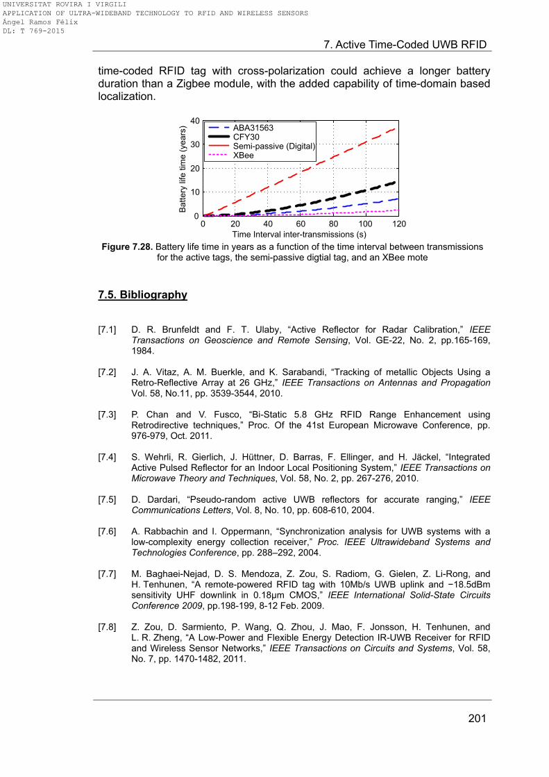
7. Active Time-Coded UWB RFID
201
time-coded RFID tag with cross-polarization could achieve a longer battery duration than a Zigbee module, with the added capability of time-domain based localization.
0 20 40 60 80 100 1200
10
20
30
40
Time Interval inter-transmissions (s)
Ba
tte
ry life
tim
e (
ye
ars
)
ABA31563CFY30Semi-passive (Digital)XBee
Figure 7.28. Battery life time in years as a function of the time interval between transmissions
for the active tags, the semi-passive digtial tag, and an XBee mote
7.5. Bibliography [7.1] D. R. Brunfeldt and F. T. Ulaby, “Active Reflector for Radar Calibration,” IEEE
Transactions on Geoscience and Remote Sensing, Vol. GE-22, No. 2, pp.165-169, 1984.
[7.2] J. A. Vitaz, A. M. Buerkle, and K. Sarabandi, “Tracking of metallic Objects Using a
Retro-Reflective Array at 26 GHz,” IEEE Transactions on Antennas and Propagation Vol. 58, No.11, pp. 3539-3544, 2010.
[7.3] P. Chan and V. Fusco, “Bi-Static 5.8 GHz RFID Range Enhancement using
Retrodirective techniques,” Proc. Of the 41st European Microwave Conference, pp. 976-979, Oct. 2011.
[7.4] S. Wehrli, R. Gierlich, J. Hüttner, D. Barras, F. Ellinger, and H. Jäckel, “Integrated
Active Pulsed Reflector for an Indoor Local Positioning System,” IEEE Transactions on Microwave Theory and Techniques, Vol. 58, No. 2, pp. 267-276, 2010.
[7.5] D. Dardari, “Pseudo-random active UWB reflectors for accurate ranging,” IEEE
Communications Letters, Vol. 8, No. 10, pp. 608-610, 2004.
[7.6] A. Rabbachin and I. Oppermann, “Synchronization analysis for UWB systems with a low-complexity energy collection receiver,” Proc. IEEE Ultrawideband Systems and Technologies Conference, pp. 288–292, 2004.
[7.7] M. Baghaei-Nejad, D. S. Mendoza, Z. Zou, S. Radiom, G. Gielen, Z. Li-Rong, and
H. Tenhunen, “A remote-powered RFID tag with 10Mb/s UWB uplink and −18.5dBm sensitivity UHF downlink in 0.18μm CMOS,” IEEE International Solid-State Circuits Conference 2009, pp.198-199, 8-12 Feb. 2009.
[7.8] Z. Zou, D. Sarmiento, P. Wang, Q. Zhou, J. Mao, F. Jonsson, H. Tenhunen, and
L. R. Zheng, “A Low-Power and Flexible Energy Detection IR-UWB Receiver for RFID and Wireless Sensor Networks,” IEEE Transactions on Circuits and Systems, Vol. 58, No. 7, pp. 1470-1482, 2011.
UNIVERSITAT ROVIRA I VIRGILI APPLICATION OF ULTRA-WIDEBAND TECHNOLOGY TO RFID AND WIRELESS SENSORS Ángel Ramos Félix DL: T 769-2015
Application of Ultra-Wideband Technology to RFID and Wireless Sensors
202
[7.9] S. Krishnan, V. Pillai, and W. Wenjiang, “UWB-IR Active Reflector for High Precision Ranging and Positioning Applications,” 2010 IEEE International Conference on Communication Systems (ICCS), pp.14-18, 2010.
[7.10] Z. N. Chen, X. Qing, and H. L. Chung, “A Universal UHF RFID Reader Antenna”, IEEE
Transactions on Microwave Theory and Techniques, Vol. 57, No. 5, pp.1275-1282, 2009.
[7.11] M. G. Di Benedetto, T. Kaiser, A. F. Molish, I. Oppermann, C. Politano, and D. Porcino, “UWB Communications Systems: A Comprehensive Overview,” Erasip Signal Processing and Communications, ISBN 9775945100.
[7.12] Time Domain, “PulsON P400 MRM,” http://www.timedomain.com/p400-mrm.php, Nov. 2014 [Nov. 1, 2014].
[7.13] R. D‟Errico, et. al., “An UWB-UHF Semi-Passive RFID System for Localization and Tracking Applications”, IEEE 2012 International Conference on RFID Technology and Applications, pp.18-23, 2012.
[7.14] Avago Technologies, “HSMS-285x Series Surface Mount Zero Bias Schottky Detector Diodes,” http://www.avagotech.com/docs/AV02-1377EN, Nov. 2014 [Nov. 1, 2014].
[7.15] Microwave Vision Group - Satimo, "Open Boundary Quad Ridge Horns," Datasheet (QH2000), 2014.
[7.16] Digi International Inc, “XBee® 802.15.4 - Device connectivity using multiport wireless networks,” Specification, 2015.
UNIVERSITAT ROVIRA I VIRGILI APPLICATION OF ULTRA-WIDEBAND TECHNOLOGY TO RFID AND WIRELESS SENSORS Ángel Ramos Félix DL: T 769-2015
8. Chipless Frequency-Coded RFID Tag Detection using STFT
203
8. Chipless Frequency-Coded RFID Tag Detection using Short-Time Fourier Transform
The work explained in this chapter has been developed during a 3-month research period at the Laboratoire de Conception et d’Intégration des Systèmes (LCIS), Valence, France.
This chapter presents a technique based on the short-time Fourier transform to detect depolarizing frequency-coded chipless RFID tags. The detection exploits a temporal separation that allows to obtain the ID with only one measurement. This temporal separation is possible when the tag presents a long-time signature, longer than the backscattering wave corresponding to the surrounding objects. A technique based on the short-time Fourier transform is used to differentiate the useful parts of the signal which contain the tag ID. Up to now, this was done by using a calibration process based on two measurements at least to remove coupling and clutter contribution. With the proposed approach the acquisition of the tag ID is direct, and it is not necessary to have further information such as the measurement the environment without the tag (background). A study on the time duration of several frequency-coded tags is performed, based on simulations and measurements. The study shows that this approach can be used with classical depolarizing chipless tags already proposed in the literature. It is proven that the proposed approach is useful to detect the tag response with a single measurement. 8.1. Introduction In RFID systems, the fact that objects where the tags are attached to can be considered to be unknown, as well as the fact that the environment can change during the reading, are specific features that require huge considerations, notably during the tag design process [8.1]. Chipless tags operating in the frequency domain (also known as frequency-coded) are known to be more efficient in terms of coding capacity [8.2]. Currently, one of main challenges of chipless frequency-coded RFID is the robustness of tag detection in different environments [8.3-8.5]. It is useless to try to increase the quantity of information that a chipless tag can have if the tag ID cannot be read properly in real environments and without complex calibration techniques. As explained in Section 2.4.1, a background subtraction is usually required to detect the ID of the tag, and it is something also necessary in frequency-coded tags [8.2-8.3]. In order to read the tag with only one measurement, specific techniques have to be implemented, aiming to to separate the contribution of the tag from the contribution of the environment. The classical approach in frequency-coded tags [8.3] concerned only the frequency domain signal. As the information is coded in frequency, the calibration process is done on the signal represented in frequency. The main contributors to the signal at the reader (1- the objects that represent the surrounding environment of the tag: object on which the tag is placed, surrounding objects, but also the antennas that are used to perform the measurements, and 2- the chipless tag) are very different, with very different
UNIVERSITAT ROVIRA I VIRGILI APPLICATION OF ULTRA-WIDEBAND TECHNOLOGY TO RFID AND WIRELESS SENSORS Ángel Ramos Félix DL: T 769-2015
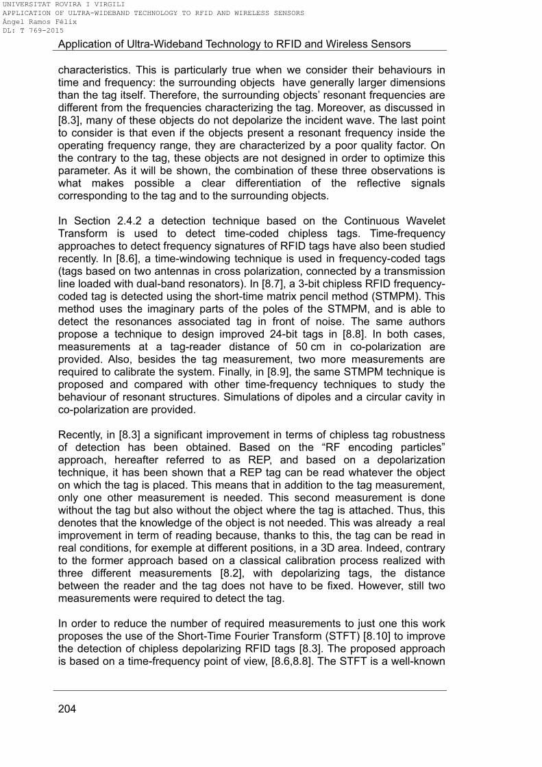
Application of Ultra-Wideband Technology to RFID and Wireless Sensors
204
characteristics. This is particularly true when we consider their behaviours in time and frequency: the surrounding objects have generally larger dimensions than the tag itself. Therefore, the surrounding objects’ resonant frequencies are different from the frequencies characterizing the tag. Moreover, as discussed in [8.3], many of these objects do not depolarize the incident wave. The last point to consider is that even if the objects present a resonant frequency inside the operating frequency range, they are characterized by a poor quality factor. On the contrary to the tag, these objects are not designed in order to optimize this parameter. As it will be shown, the combination of these three observations is what makes possible a clear differentiation of the reflective signals corresponding to the tag and to the surrounding objects.
In Section 2.4.2 a detection technique based on the Continuous Wavelet Transform is used to detect time-coded chipless tags. Time-frequency approaches to detect frequency signatures of RFID tags have also been studied recently. In [8.6], a time-windowing technique is used in frequency-coded tags (tags based on two antennas in cross polarization, connected by a transmission line loaded with dual-band resonators). In [8.7], a 3-bit chipless RFID frequency-coded tag is detected using the short-time matrix pencil method (STMPM). This method uses the imaginary parts of the poles of the STMPM, and is able to detect the resonances associated tag in front of noise. The same authors propose a technique to design improved 24-bit tags in [8.8]. In both cases, measurements at a tag-reader distance of 50 cm in co-polarization are provided. Also, besides the tag measurement, two more measurements are required to calibrate the system. Finally, in [8.9], the same STMPM technique is proposed and compared with other time-frequency techniques to study the behaviour of resonant structures. Simulations of dipoles and a circular cavity in co-polarization are provided. Recently, in [8.3] a significant improvement in terms of chipless tag robustness of detection has been obtained. Based on the “RF encoding particles” approach, hereafter referred to as REP, and based on a depolarization technique, it has been shown that a REP tag can be read whatever the object on which the tag is placed. This means that in addition to the tag measurement, only one other measurement is needed. This second measurement is done without the tag but also without the object where the tag is attached. Thus, this denotes that the knowledge of the object is not needed. This was already a real improvement in term of reading because, thanks to this, the tag can be read in real conditions, for exemple at different positions, in a 3D area. Indeed, contrary to the former approach based on a classical calibration process realized with three different measurements [8.2], with depolarizing tags, the distance between the reader and the tag does not have to be fixed. However, still two measurements were required to detect the tag. In order to reduce the number of required measurements to just one this work proposes the use of the Short-Time Fourier Transform (STFT) [8.10] to improve the detection of chipless depolarizing RFID tags [8.3]. The proposed approach is based on a time-frequency point of view, [8.6,8.8]. The STFT is a well-known
UNIVERSITAT ROVIRA I VIRGILI APPLICATION OF ULTRA-WIDEBAND TECHNOLOGY TO RFID AND WIRELESS SENSORS Ángel Ramos Félix DL: T 769-2015

8. Chipless Frequency-Coded RFID Tag Detection using STFT
205
technique for audio and speech processing. The time duration of the tag backscattering signal is much more important than the one corresponding to the whole tag environment (background). Thanks to this difference, the recovery of the tag ID is possible by taking in consideration the signal in frequency and in time together. By combining the STFT with robust depolarizing tags [8.3], the tag response can be obtained without any calibration measurements. This is possible because frequency domain depolarizing chipless tags are intrinsically resonant structures, designed to have a high quality factor in order to present a high RCS. It is why their quality factor is higher than the one coming from the surrounding objects. So the tags will store energy corresponding to their frequency of resonances, and by suppressing the early-time scattering, tag identification based on the late-time signal part could be possible [8.11]. The discrimination based on this ascertainment will be shown for several chipless resonant tag structures. This chapter is organized as follows:
Section 8.2 revises the theoretical foundations for depolarizing frequency-coded chipless RFID. The STFT theory is also explained, specifically applied to detect depolarizing chipless tags
Section 8.3 studies the quality factor of chipless tags, directly related with the proposed STFT processing technique
Section 8.4 presents measurements of depolarizing chipless tags and proves the usefulness of the STFT for detection
Finally, Section 8.5 draws the conclusions 8.2. Theory 8.2.1. Depolarizing frequency-coded chipless RFID Figure 8.1 shows a scheme of the depolarizing chipless RFID system along with the signals involved. The reader transmits a wideband vertically-polarized signal which hits the tag. The tag horizontally-polarized backscattered signal part is then received at the reader. The ID is coded in the presence or absence of resonances. The tags are composed by REPs, which act as a transmitting/receiving antenna and a filtering circuit. Following the model from [8.3], the signal at the reader can be expressed as:
vh vh vv vh hhM I R C T , (8.1)
where Ivh is the direct coupling from the reader’s transmitting to receiving antenna in cross-polarization, Rvv is the receive path in vertical polarization, Cvh is the tag response in cross-polarization, and Thh is the transmitted path in horizontal polarization. This type of tag and configuration has proven to be robust in front of surrounding objects near the tag [8.3]. The tag ID is obtained
UNIVERSITAT ROVIRA I VIRGILI APPLICATION OF ULTRA-WIDEBAND TECHNOLOGY TO RFID AND WIRELESS SENSORS Ángel Ramos Félix DL: T 769-2015
Application of Ultra-Wideband Technology to RFID and Wireless Sensors
206
by subtracting the measurements of tags Mvh from the empty measurement Ivh. It is important to note that, in such a case, a calibration procedure using a reference object is not necessary to find the ID of the tag. Indeed, even if the coefficients Rvv and Thh are not known (the distortion introduced is low enough so the peaks in frequency who encode the data are still recognizable), the tag ID can be deduced form Rvv Cvh Thh which simply corresponds to Mvh - Ivh. But Ivh is needed, that means that two measurements must be done. Even though the coupling Ivh, is cross-polarized, its power is strong enough (because of the proximity between the reader’s antennas) to prevent any reading. Moreover, as it can be observed in Figure 8.1, objects near the tag, although they do not really depolarize the incoming signal (and should have small amplitude in reception), can distort the tag response. By gating in time-domain the undesired contributions, mainly Ivh, the resonances can be detected in front of these induced perturbations. Figure 8.1b shows a scheme of the signals in detail in time domain. Time constants τI, τC can be associated to the time response (or time duration) of Ivh (t) and RvvCvhThh(t), respectively. If τI << τC, that is, the time response of the tag (and surrounding objects) is much slower than the time response of the coupling contribution, both signals can be separated, and,
therefore, ( ) ( )vh vv vh hhM t R C T t for t >> τI . Therefore, by using the late-time part
of signal, we will see that it is possible with one measurement Mvh, to extract the tag ID.
Object
2
Object 1
Freq.
Transmitted (Thh)
Backscat.
(Rvv)
Cou
plin
g (Iv
h ) Depol. Tag(Cvh)
1 1 0 1 0 1
...
Time
Object 1 Object 2
Rx Ant.V. P
ol.
Tx Ant.
H. Pol.
Reader
Mvh
Ivh
Tag
-a-
Time
Mvh (
t)
τI
τC
Time
Ivh (t)
RvvCvhThh (t)
Time
Envelope
-b-
Figure 8.1. (a) Scheme of the depolarizing chipless RFID system. (b) Scheme of the signals in time domain
8.2.2. Short-Time Fourier Transform
The Short-Time Fourier Transform of a given signal s(t) can be defined as [8.10,8.12]:
UNIVERSITAT ROVIRA I VIRGILI APPLICATION OF ULTRA-WIDEBAND TECHNOLOGY TO RFID AND WIRELESS SENSORS Ángel Ramos Félix DL: T 769-2015
8. Chipless Frequency-Coded RFID Tag Detection using STFT
207
( , ) ( ) ( ) j tS s t w t e dt
, (8.2)
where ω = 2πf is the angular frequency and τ is the time across w(t) is shifted. w(t) is a weighting function or time window, i.e., the impulse response of a lowpass filter. It is desired that w(t) has a finite impulse response (FIR), or duration in time. The STFT can be seen as the Fourier transform of a time weighted signal, where τ is the time where the weighting function w(t) is centered. This transform can also be seen as the output of a complex baseband filter bank. As explained in Section 8.2.1, frequency-coded chipless tags rely on the presence or absence of resonances (peaks) within a wide band. In this case, ω is the center frequency of each bandpass filter and τ is the time when the filter output is sampled. In order to derive the filter bank interpretation, the impulse response of the bandpass filter can be expressed as:
( ) ( ) j th t w t e
. (8.3)
Then, (8.2) can be expressed as:
( )( , ) ( ) ( ) ( ) ( )
( ) ( ) .
j t j j t
j
S w t e s t e s t w t e dt
e h t s t
(8.4)
Therefore, the STFT can be seen as the demodulated (by je ) bandpass
filtered signal from s(t). Since w(t) is lowpass, S(ω,τ) is a lowpass function of τ. Then, for each ω, S can be sampled at a rate determined by twice the lowpass cutoff frequency (fc) of the window w(t) (from Nyquist’s Theorem). The window w(t) plays the most important role in the STFT, since there is a tradeoff between time-limiting and bandwidth-limiting. Concerning frequency-coded tags, a time-limited signal can separate better the coupling and clutter contributions from the actual tag response. However, in this case the frequency peaks of associated to the tag ID are wider and difficult to separate. On the contrary, a bandwidth-limited window can provide sharp tag ID peaks, at the cost of including more unwanted signal contributions inside the window [8.9]. Three typically-used windows are considered to detect the tags: Hamming, Chebyschev and Kaiser [8.13]. Figure 8.2 shows the calculated time-domain response of the three windows considered, along with a rectangular window. For the Chebyschev windows, attenuations of the sidelobes of 30 dB and 100 dB have been considered, while for the Kaiser windows, 3 dB and 100 dB. A Hamming window is chosen as a tradeoff solution to have enough resolution both in time and frequency domain.
Chossing a correct window length is as important as the shape. Figure 8.3 shows a scheme of the time-domain response of a chipless RFID tag. The
UNIVERSITAT ROVIRA I VIRGILI APPLICATION OF ULTRA-WIDEBAND TECHNOLOGY TO RFID AND WIRELESS SENSORS Ángel Ramos Félix DL: T 769-2015

Application of Ultra-Wideband Technology to RFID and Wireless Sensors
208
“Calibrated” signal accounts for the tag response after subtracting the background (empty-room scene). The window w(t) is also shown. As observed, coupling (Ivh, as detailed in Section 8.2.1) and clutter contributions appear. If a very long window is chosen more noise is captured inside the window, reducing the SNR. At the limit, the coupling contribution (which is the main undesired contribution to remove from the real tag’s response) could be inside the window for any τ. Even though it requires more processing time, window overlapping is also used in order to avoid data loss near the window boundaries [8.13]. The window length T will be chosen according to the results from Section 8.3.
0 2 4 6 8 10 120
0.2
0.4
0.6
0.8
1
Time (ns)
No
rma
lize
d A
mp
litu
de
RectangularHamming
Cheb. 30 dB
Cheb. 100 dB
Kais. 3 dB
Kais. 100 dB
Figure 8.2. Calculated time-domain response of several windows w(t)
0 5 10 30-1
-0.5
0
0.5
1
Time (ns)
No
rma
lize
d A
mp
litu
de
Uncal. TagCalibrated Tag
Coupling
ClutterWindow w(t)
T
τ
Figure 8.3. Scheme of the time-domain response for a frequency-coded chipless RFID tag
8.3. Quality factor of REP tags REP-based tags with high quality factors [8.14] are required to apply the STFT, since a long duration in time domain is needed. In order to study this, a single dipole (with no ground plane) in co-polarization is simulated using Ansys HFSS. It is simulated with Rogers RO4003 substrate (see Table 2.3), with an incident plane wave and vacuum box of 40 cm. The dipole width is changed from 1 to 10 mm. The tag is simulated from 1 to 10 GHz. Figure 8.4 shows the time domain response (with inverse Fourier transform) from the probe, up to 1.6 ns. In the bottom inset, the simulated dipole is shown. In the top insets, the signal is shown for two instants. As it can be observed, the early-time response (so-called structural mode), which depends on the tag shape, size and material, is
UNIVERSITAT ROVIRA I VIRGILI APPLICATION OF ULTRA-WIDEBAND TECHNOLOGY TO RFID AND WIRELESS SENSORS Ángel Ramos Félix DL: T 769-2015
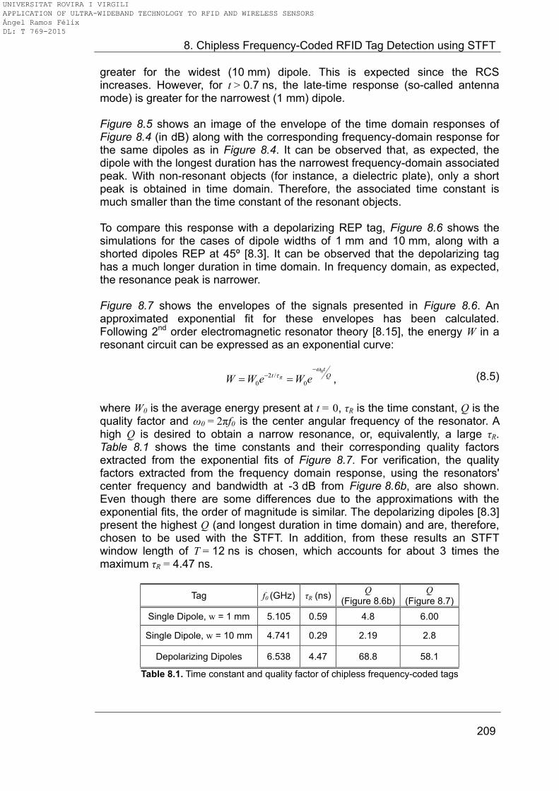
8. Chipless Frequency-Coded RFID Tag Detection using STFT
209
greater for the widest (10 mm) dipole. This is expected since the RCS increases. However, for t > 0.7 ns, the late-time response (so-called antenna mode) is greater for the narrowest (1 mm) dipole. Figure 8.5 shows an image of the envelope of the time domain responses of Figure 8.4 (in dB) along with the corresponding frequency-domain response for the same dipoles as in Figure 8.4. It can be observed that, as expected, the dipole with the longest duration has the narrowest frequency-domain associated peak. With non-resonant objects (for instance, a dielectric plate), only a short peak is obtained in time domain. Therefore, the associated time constant is much smaller than the time constant of the resonant objects. To compare this response with a depolarizing REP tag, Figure 8.6 shows the simulations for the cases of dipole widths of 1 mm and 10 mm, along with a shorted dipoles REP at 45º [8.3]. It can be observed that the depolarizing tag has a much longer duration in time domain. In frequency domain, as expected, the resonance peak is narrower. Figure 8.7 shows the envelopes of the signals presented in Figure 8.6. An approximated exponential fit for these envelopes has been calculated. Following 2nd order electromagnetic resonator theory [8.15], the energy W in a resonant circuit can be expressed as an exponential curve:
02 /
0 0R
tt QW W e W e
, (8.5)
where W0 is the average energy present at t = 0, τR is the time constant, Q is the quality factor and ω0 = 2πf0 is the center angular frequency of the resonator. A high Q is desired to obtain a narrow resonance, or, equivalently, a large τR. Table 8.1 shows the time constants and their corresponding quality factors extracted from the exponential fits of Figure 8.7. For verification, the quality factors extracted from the frequency domain response, using the resonators' center frequency and bandwidth at -3 dB from Figure 8.6b, are also shown. Even though there are some differences due to the approximations with the exponential fits, the order of magnitude is similar. The depolarizing dipoles [8.3] present the highest Q (and longest duration in time domain) and are, therefore, chosen to be used with the STFT. In addition, from these results an STFT window length of T = 12 ns is chosen, which accounts for about 3 times the maximum τR = 4.47 ns.
Tag f0 (GHz) τR (ns) Q
(Figure 8.6b) Q
(Figure 8.7)
Single Dipole, w = 1 mm 5.105 0.59 4.8 6.00
Single Dipole, w = 10 mm 4.741 0.29 2.19 2.8
Depolarizing Dipoles 6.538 4.47 68.8 58.1
Table 8.1. Time constant and quality factor of chipless frequency-coded tags
UNIVERSITAT ROVIRA I VIRGILI APPLICATION OF ULTRA-WIDEBAND TECHNOLOGY TO RFID AND WIRELESS SENSORS Ángel Ramos Félix DL: T 769-2015
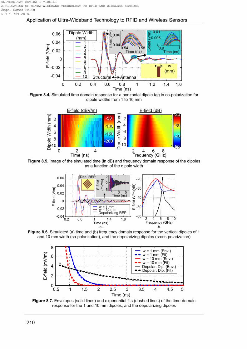
Application of Ultra-Wideband Technology to RFID and Wireless Sensors
210
0.54 0.580.04
0.06
Time (ns)
E-f
ield
(V
/m)
0 0.2 0.4 0.6 0.8 1 1.2 1.4 1.6
-0.04
-0.02
0
0.02
0.04
0.06
Time (ns)
E-f
ield
(V
/m)
0.9 10
0.005
0.01
Time (ns)E-f
ield
(V
/m)
w
(mm)
123456789
10
Dipole Width
(mm)
Structural Antenna
Figure 8.4. Simulated time domain response for a horizontal dipole tag in co-polarization for
dipole widths from 1 to 10 mm
Frequency (GHz)2 4 6 8
Time (ns)
Dip
ole
Wid
th (
mm
)
0 2 4
2
4
6
8
10
E-field (dBV/m)
-200-200
-150-150
-100-100
-50-50
-50-50
-40-40
-30-30
-20-20D
ipole
Wid
th (
mm
)2
4
6
8
10
E-field (dB)
Figure 8.5. Image of the simulated time (in dB) and frequency domain response of the dipoles
as a function of the dipole width
0.2 0.6 1 1.4 1.8-0.04
-0.02
0
0.02
0.04
0.06
Time (ns)
E-f
ield
(V
/m)
1 3 5-5
0
5
Time (ns)
E-f
ield
(mV
/m)
2 4 6 8 10-60
-50
-40
-30
-20
Frequency (GHz)
E-f
ield
(V
/m)(
dB
)
w = 1 mmw = 10 mmDepolarizing REP
Dep. REP
-a- -b- Figure 8.6. Simulated (a) time and (b) frequency domain response for the vertical dipoles of 1
and 10 mm width (co-polarization), and the depolarizing dipoles (cross-polarization)
0.5 1 1.5 2 2.5 3 3.5 4 4.5 50
2
4
6
8
Time (ns)
E-f
ield
(m
V/m
)
w = 1 mm (Env.)w = 1 mm (Fit)w = 10 mm (Env.)w = 10 mm (Fit)Depolar. Dip. (Env.)Depolar. Dip. (Fit)
Figure 8.7. Envelopes (solid lines) and exponential fits (dashed lines) of the time-domain
response for the 1 and 10 mm dipoles, and the depolarizing dipoles
UNIVERSITAT ROVIRA I VIRGILI APPLICATION OF ULTRA-WIDEBAND TECHNOLOGY TO RFID AND WIRELESS SENSORS Ángel Ramos Félix DL: T 769-2015

8. Chipless Frequency-Coded RFID Tag Detection using STFT
211
8.4. Measurements 8.4.1. Measurement setup and tags The reader consists of an Agilent N5224A Vector Network Analyzer (VNA). The frequency is swept from 3 to 10 GHz, with 10001 points. A dual-access dual-polarization Satimo QH2000 antenna [8.16] is connected to the VNA ports 1 and 2, in horizontal and vertical polarization, respectively. This antenna presents gain between 3 – 16 dBi at 2 – 32 GHz, and isolation greater than 30 dB between ports. The tags are measured inside and outside an anechoic chamber. Figure 8.8 shows a photograph of the experimental setup outside the chamber. Figure 8.9 shows the measured |S21| parameter for the tag with shorted 45º dipoles and for the tag with dual-L resonators described in [8.3]. The measurement is performed inside an anechoic chamber at a 30 cm tag-reader distance. As already said, in [8.3], two measurements had to be performed: the measurement S21 with the tag and the S21Back or background (empty-room scene) without the presence of the tag. Then, the tag response was obtained by subtracting S21Back from S21. As it can be observed in Figure 8.9, in normal conditions, if the background is not subtracted, the resonances associated to the tag ID cannot be obtained (even if we observe some variations around the expected frequency of resonances, these variations are too low to be used for detection), even inside an anechoic chamber in optimum conditions.
FoamFoam
Depolarizing TagDepolarizing Tag
P2 R
x
(V. P
ol)
P2 R
x
(V. P
ol)
P1 Tx
(H. Pol)
P1 Tx
(H. Pol)
Rea
der
Ante
nn
a
Rea
der
Ante
nn
a
VNAVNA
Figure 8.8. Photograph of the measurement setup
8.4.2. Using the STFT to detect depolarizing tags Next, the STFT is applied to the uncalibrated signals for the shorted dipoles and the dual-L resonators, under the conditions of Section 8.4.1. Figure 8.10 shows the obtained spectrogram using a Hamming window. The actual frequencies of the resonators are shown on top. It can be seen that for small values of τ (window at early delay) the resonances are blurred with respect to the noise. This occurs because the coupling (Ivh) and the tag structural mode are inside the window. However, when the window is shifted at a later delay, only the antenna mode (associated to the actual resonances in time domain) is captured. At the last values of τ, the window is outside both the structural and antenna mode, and therefore only the first resonances with higher quality
UNIVERSITAT ROVIRA I VIRGILI APPLICATION OF ULTRA-WIDEBAND TECHNOLOGY TO RFID AND WIRELESS SENSORS Ángel Ramos Félix DL: T 769-2015
Application of Ultra-Wideband Technology to RFID and Wireless Sensors
212
factors can be observed.
|S21
| (d
B)
3 4 5 6 7 8 9 10
Frequency (GHz)
-20
-10
0 12 3 4 5 6
-20
-10
0
Norm
aliz
ed Uncalibrated
Background sub.
1 23
4 5 6 7 8 Bit Number
-a-
-b-
Figure 8.9. Measured |S21| for the tags without (solid black line) and with (red dashed line) the background measurement at 30 cm inside an anechoic chamber. (a) Shorted dipoles at 45º.
(b): Dual-L resonators
10
15 20
(ns)
Fre
qu
ency (
GH
z)
|S2
1|
-45-45
-30-30
-15-15
00(d
B)
3
4
5
6
7
3
4
5
6
78.8
0
6.9
8
18
.18
-a-
-b-
Figure 8.10. STFT Spectrogram for the (a) shorted 45º dipoles and (b) dual-L dipoles using a
Hamming window, at 30 cm inside an anechoic chamber. The expected frequency peaks are in dashed black lines
UNIVERSITAT ROVIRA I VIRGILI APPLICATION OF ULTRA-WIDEBAND TECHNOLOGY TO RFID AND WIRELESS SENSORS Ángel Ramos Félix DL: T 769-2015
8. Chipless Frequency-Coded RFID Tag Detection using STFT
213
Figure 8.11a shows a cut at τ = 10 ns of the STFT spectrogram. The reference with background subtraction is also shown. As it can be observed, with a single measurement most of the resonances can be obtained by applying this method. It is important to note that the quality factor of each resonator is different, as it can be observed in the results obtained with background subtraction. As shown in Figure 8.10, there are several resonators which are not detected properly at τ = 10 ns. For instance, the 3rd resonator for the shorted 45º dipoles (top of Figure 8.11a) has a different quality factor from their neighbours, and, therefore, it is not detected properly. Figure 8.11b shows cuts at τ = 6.98, 8.80, 10.72 and
18.18 ns. The expected frequencies (from the background subtracted reference) are also shown. As it can be observed, depending on the value of τ there are resonances that can be recovered: the 3rd resonator of the shorted 45º dipoles and the 5th resonator of the dual-L dipoles. Finally, the shorted 45º dipoles tag is measured in outside the anechoic chamber (in a typical laboratory scenario), at 40 cm, and with an object near its environment (a block of paper). Then, the STFT is applied, and the corresponding spectrogram is shown in Figure 8.12. A cut of the spectrogram, again at τ = 10 ns, is shown in Figure 8.13a. Most of the resonances can be extracted even in a realistic environment with an object near the tag. Following the procedure in Figure 8.11b, Figure 8.13b shows the same STFT cuts at τ = 6.98, 8.80, 10.72 and 18.18 ns. It can be observed that, in a realistic scenario with a near object, due to the high level of noise, it is not possible to recover the 5th and 8th peaks with different τ values. It is clear from the results presented in Figures 8.10 and 8.12 that a specifically designed tag would present even better results. In this case, it is possible to adjust de widths of the higher resonators in order to increase their quality factor. By doing this, the data extraction with a constant value of τ could be done with higher accuracy. Detection based on image processing could also improve significantly the approach. In that case, the data would be obtained not from discrete values of τ but with the entire information contained in the 2D STFT Spectrogram. Last but not least, this approach could also be applied on classical approaches with the calibrated signal (with a background measurement) in complex scenarios. 8.5. Conclusion This chapter has presented a detection technique for frequency-coded chipless
RFID tags, based on the Short-Time Fourier Transform. The technique consists
of filtering in time-domain the tag signal, avoiding coupling and clutter
contributions. A study of the time-domain duration of chipless tags is performed,
proving that depolarizing tags have a long time duration, and hence are good
candidates for this technique. Combining the technique with depolarizing tags,
no calibration (background or empty-room response) is required.
UNIVERSITAT ROVIRA I VIRGILI APPLICATION OF ULTRA-WIDEBAND TECHNOLOGY TO RFID AND WIRELESS SENSORS Ángel Ramos Félix DL: T 769-2015
Application of Ultra-Wideband Technology to RFID and Wireless Sensors
214
3 3.5 4 4.5 5 5.5 6 6.5 7
-40
-30
-20
-10
0
Frequency (GHz)
Norm
aliz
ed |S
21| (d
B)
1 2 3 4 5 6 7 8
-30
-20
-10
0
1 2 3 4
Background sub.STFT at = 10 ns
5 6Bit Number
-a-
3 3.5 4 4.5 5 5.5 6 6.5 7-30
-20
-10
0
Frequency (GHz)
-30
-20
-10
0
No
rma
lize
d |S
21| (d
B)
6.98 8.80 10.72 18.18τ (ns)
-b-
Figure 8.11. (a) Background subtracted reference (red dashed line) and cut at τ = 10 ns of the STFT Spectrogram (solid black line); and (b) cuts at τ = 6.98, 8.80, 10.72, and 18.18 ns of the
STFT Spectrogram for the shorted 45º dipoles and dual-L dipoles at 30 cm inside an anechoic chamber
UNIVERSITAT ROVIRA I VIRGILI APPLICATION OF ULTRA-WIDEBAND TECHNOLOGY TO RFID AND WIRELESS SENSORS Ángel Ramos Félix DL: T 769-2015
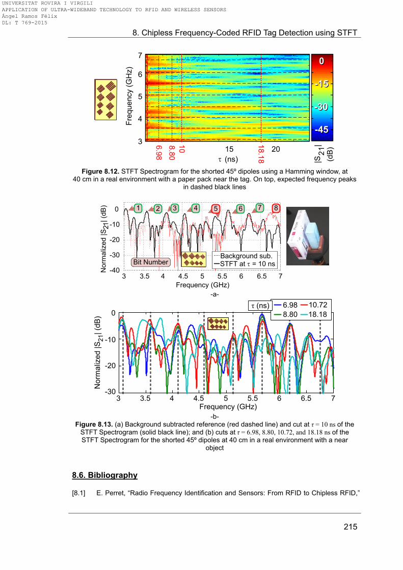
8. Chipless Frequency-Coded RFID Tag Detection using STFT
215
15 20
(ns)
Fre
qu
en
cy (
GH
z)
|S2
1|
-45-45
-30-30
-15-15
00
(dB
)
3
4
5
6
7
108.8
0
6.9
8
18
.18
Figure 8.12. STFT Spectrogram for the shorted 45º dipoles using a Hamming window, at
40 cm in a real environment with a paper pack near the tag. On top, expected frequency peaks in dashed black lines
3 3.5 4 4.5 5 5.5 6 6.5 7-40
-30
-20
-10
0
Frequency (GHz)
No
rma
lize
d |S
21| (d
B)
Bit Number
1 2 3 4 6 7 85
Background sub.STFT at = 10 ns
-a-
3 3.5 4 4.5 5 5.5 6 6.5 7-30
-20
-10
0
Frequency (GHz)
Norm
aliz
ed |S
21| (d
B)
6.98
8.80
10.72
18.18
τ (ns)
-b-
Figure 8.13. (a) Background subtracted reference (red dashed line) and cut at τ = 10 ns of the STFT Spectrogram (solid black line); and (b) cuts at τ = 6.98, 8.80, 10.72, and 18.18 ns of the STFT Spectrogram for the shorted 45º dipoles at 40 cm in a real environment with a near
object
8.6. Bibliography [8.1] E. Perret, “Radio Frequency Identification and Sensors: From RFID to Chipless RFID,”
UNIVERSITAT ROVIRA I VIRGILI APPLICATION OF ULTRA-WIDEBAND TECHNOLOGY TO RFID AND WIRELESS SENSORS Ángel Ramos Félix DL: T 769-2015
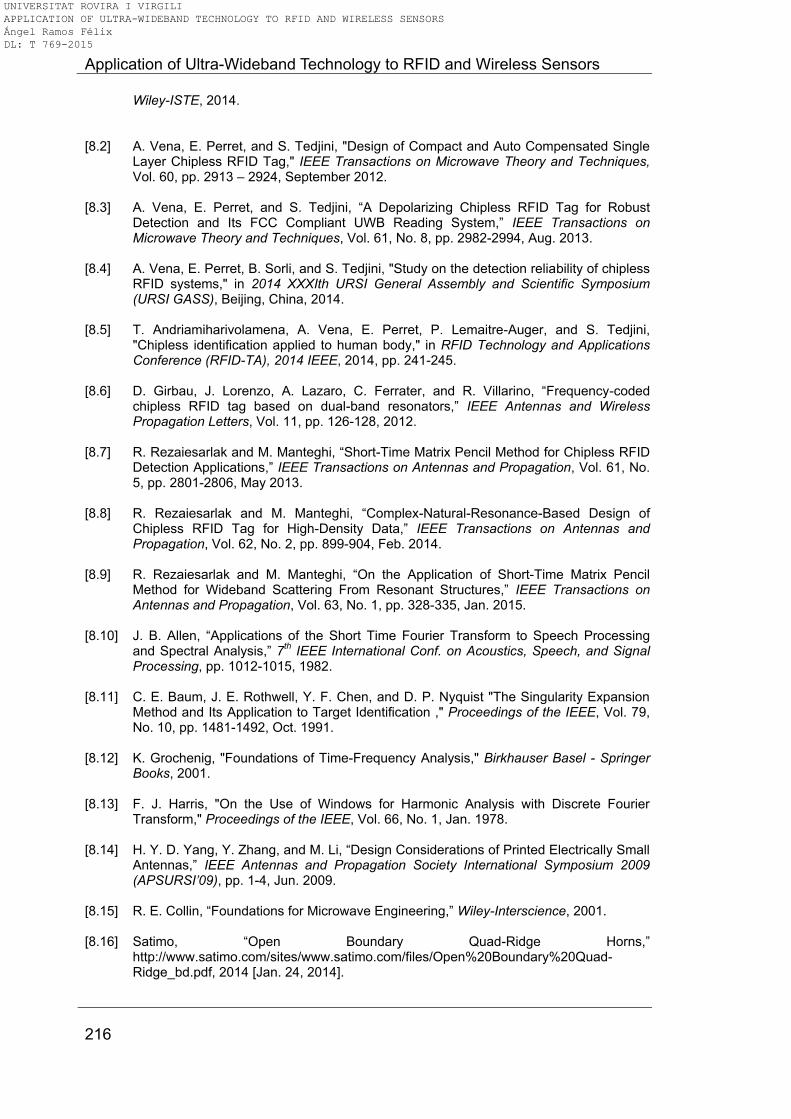
Application of Ultra-Wideband Technology to RFID and Wireless Sensors
216
Wiley-ISTE, 2014.
[8.2] A. Vena, E. Perret, and S. Tedjini, "Design of Compact and Auto Compensated Single
Layer Chipless RFID Tag," IEEE Transactions on Microwave Theory and Techniques, Vol. 60, pp. 2913 – 2924, September 2012.
[8.3] A. Vena, E. Perret, and S. Tedjini, “A Depolarizing Chipless RFID Tag for Robust
Detection and Its FCC Compliant UWB Reading System,” IEEE Transactions on Microwave Theory and Techniques, Vol. 61, No. 8, pp. 2982-2994, Aug. 2013.
[8.4] A. Vena, E. Perret, B. Sorli, and S. Tedjini, "Study on the detection reliability of chipless
RFID systems," in 2014 XXXIth URSI General Assembly and Scientific Symposium (URSI GASS), Beijing, China, 2014.
[8.5] T. Andriamiharivolamena, A. Vena, E. Perret, P. Lemaitre-Auger, and S. Tedjini,
"Chipless identification applied to human body," in RFID Technology and Applications Conference (RFID-TA), 2014 IEEE, 2014, pp. 241-245.
[8.6] D. Girbau, J. Lorenzo, A. Lazaro, C. Ferrater, and R. Villarino, “Frequency-coded
chipless RFID tag based on dual-band resonators,” IEEE Antennas and Wireless Propagation Letters, Vol. 11, pp. 126-128, 2012.
[8.7] R. Rezaiesarlak and M. Manteghi, “Short-Time Matrix Pencil Method for Chipless RFID
Detection Applications,” IEEE Transactions on Antennas and Propagation, Vol. 61, No. 5, pp. 2801-2806, May 2013.
[8.8] R. Rezaiesarlak and M. Manteghi, “Complex-Natural-Resonance-Based Design of
Chipless RFID Tag for High-Density Data,” IEEE Transactions on Antennas and Propagation, Vol. 62, No. 2, pp. 899-904, Feb. 2014.
[8.9] R. Rezaiesarlak and M. Manteghi, “On the Application of Short-Time Matrix Pencil
Method for Wideband Scattering From Resonant Structures,” IEEE Transactions on Antennas and Propagation, Vol. 63, No. 1, pp. 328-335, Jan. 2015.
[8.10] J. B. Allen, “Applications of the Short Time Fourier Transform to Speech Processing
and Spectral Analysis,” 7th IEEE International Conf. on Acoustics, Speech, and Signal
Processing, pp. 1012-1015, 1982.
[8.11] C. E. Baum, J. E. Rothwell, Y. F. Chen, and D. P. Nyquist "The Singularity Expansion Method and Its Application to Target Identification ," Proceedings of the IEEE, Vol. 79, No. 10, pp. 1481-1492, Oct. 1991.
[8.12] K. Grochenig, "Foundations of Time-Frequency Analysis," Birkhauser Basel - Springer
Books, 2001.
[8.13] F. J. Harris, "On the Use of Windows for Harmonic Analysis with Discrete Fourier Transform," Proceedings of the IEEE, Vol. 66, No. 1, Jan. 1978.
[8.14] H. Y. D. Yang, Y. Zhang, and M. Li, “Design Considerations of Printed Electrically Small
Antennas,” IEEE Antennas and Propagation Society International Symposium 2009 (APSURSI’09), pp. 1-4, Jun. 2009.
[8.15] R. E. Collin, “Foundations for Microwave Engineering,” Wiley-Interscience, 2001.
[8.16] Satimo, “Open Boundary Quad-Ridge Horns,”
http://www.satimo.com/sites/www.satimo.com/files/Open%20Boundary%20Quad-Ridge_bd.pdf, 2014 [Jan. 24, 2014].
UNIVERSITAT ROVIRA I VIRGILI APPLICATION OF ULTRA-WIDEBAND TECHNOLOGY TO RFID AND WIRELESS SENSORS Ángel Ramos Félix DL: T 769-2015
9. General Conclusions
217
9. General Conclusions This Doctoral Thesis has studied the application of UWB technology to RFID. Chipless, semi-passive and active time-coded UWB RFID approaches have been proposed. Each approach has shown its advantages or disadvantages over the other approaches in terms of cost, complexity, reliability and read range. Chipless time-coded UWB RFID is very simple, low-cost but more prone to detection errors. Semi-passive time-coded UWB RFID is more complex and requires a power source, but extends the read range of chipless as well as it increases the possible applications and minimizes the detection errors or misreads. Finally, active time-coded UWB RFID has been proposed as a long-range alternative, with a high power consumption compared to semi-passive, but ideal for localization applications. Both commercial and in-development sensors have been integrated with the proposed approaches. Real-case sensor measurements have shown the proposed systems’ feasibility. Finally, a smart floor application combining time-coded UWB RFID and GPR technologies has been proposed. The theory for time-coded UWB RFID, as well as the signal processing techniques (required for optimum detection), have been developed. Also, commercial UWB radars have been proposed as low-cost readers. It has been proven that integrating UWB antennas with delay lines in the same substrate is possible, but it is not a straightforward process and needs a studied structure. It has been shown that time-coded chipless UWB tags, fabricated on flexible substrates, are still readable when they are bent. Circular polarization has been achieved by using circularly-polarized UWB antennas, and therefore solving the problem of tag orientation in E-plane. In addition, it has been shown that materials on the back of UWB chipless tags neither detune nor affect their performance thanks to the tags’ wideband nature. A real scenario indoor read range of about 2 meters has been demonstrated. However, it has been shown that the number of possible IDs in time-coded chipless tags is small when compared to chip-based EPC tags or even frequency-coded chipless tags. Therefore, more advanced sensor applications (where it is not required a large number of IDs) have been studied as the most suitable application. Two approaches have been presented for implementing wireless sensors using chipless time-coded UWB RFID tags. It has been demonstrated that it is possible to use the delay or amplitude of the tag response to sense physical parameters. It has also been shown that self-calibration is possible with specific designs, increasing the reliability of chipless sensors. As examples of low-cost chipless sensor designs, continuous temperature sensors and thermal threshold detectors have been proposed using the amplitude of the tag response. The other option is based on using the delay of the tag response. Using this option, chipless permittivity sensors have been developed. A practical application for concrete composition detection has been shown. It has been proved that it is possible to classify different compositions of concrete, which is a point of interest in civil engineering and long-term monitoring of constructions.
UNIVERSITAT ROVIRA I VIRGILI APPLICATION OF ULTRA-WIDEBAND TECHNOLOGY TO RFID AND WIRELESS SENSORS Ángel Ramos Félix DL: T 769-2015
Application of Ultra-Wideband Technology to RFID and Wireless Sensors
218
Analog and digital semi-passive wireless sensing platforms using time-coded UWB RFID have been proposed. The reader interrogates a tag which is normally in a low-power sleep mode. A narrowband wake-up link has been proposed, enabling the reader to send commands to the tag. When used in crowded frequency bands such as ISM, this link has proven to be able to coexist with them. The digital platform has been achieved by means of a low-power commercial microcontroller as the core logic and a PIN diode as the backscattering element. A digital communication protocol has been designed in order to communicate and synchronize the reader and the tag. The analog platform has been achieved by means of operational amplifiers and DC switches. For the analog platform, two approaches for the backscattering element have been presented: an RF switch and a PIN diode. The RF switch approach is more expensive but its consumption is smaller than the PIN diode approach. The digital platform is scalable, more robust but also consumes more power when reading sensors and is more expensive than the analog platform, which is simpler and potentially cheaper. Overall, both platforms have obtained longer read ranges and more reliable measurements than chipless aproaches. A solar-powered temperature sensor has been proposed using the analog platform based on PIN diode. A nitrogen dioxide gas sensor, based on carbon nanotubes, has been proposed. The carbon nanotubes have been integrated in the platform based on RF switch. Concentrations as low as 10 ppm have been read wirelessly with the proposed system. Finally, several commercial analog and digital (by means of the I2C bus) sensors have been integrated in the digital platform, providing a multi-sensor tag with long-term storage capabilities. A temperature sensor, an accelerometer, a humidity sensor, a barometer and a non-volatile memory have created a tag intended for smart cities applications. The combination of chipless and semi-passive time-coded UWB RFID with ground penetration radar technology has been proposed for smart floor applications. Indoor guidance has shown to be possible with three different approaches: metal strip reflectors, chipless and semi-passive time-coded UWB RFID tags. The less complex and less expensive approach, based on metal strip reflectors, also has shown to be more difficult to be detected in front of chipless or semi-passive approaches. The semi-passive approach has been presented for special cases where advanced sensors were intended to be buried in the ground. Further work should focus in combining these approaches. Active time-coded UWB RFID platforms for long-range applications have been studied. Two approaches have been presented, one based on a reflection amplifier and the other based on an amplifier in cross polarization. The approach based on a reflection amplifier has only slightly increased the read-range with respect to semi-passive time-coded UWB RFID, despite its much larger power consumption. However, the approach based on an amplifier between two UWB antennas in cross polarization, has obtained a very long read range with respect to semi-passive cases. Indoor localization applications can benefit from using the time-domain nature of UWB, where techniques based on the time-of-arrival can be applied.
UNIVERSITAT ROVIRA I VIRGILI APPLICATION OF ULTRA-WIDEBAND TECHNOLOGY TO RFID AND WIRELESS SENSORS Ángel Ramos Félix DL: T 769-2015
9. General Conclusions
219
Finally, a signal processing technique based on the Short-Time Fourier Transform for depolarizing frequency-coded tags has been presented. The coupling between the reader’s antennas and undesired clutter at the tag-reader scene has been reduced with the proposed technique. The relationship between the time duration and the quality factor of the resonators which comprise the depolarizing tags has been studied. Using the proposed technique, most of the frequency signature (ID) of depolarizing tags has been detected with a single measurement, without the need for a background subtraction technique. To commercialize the prototypes developed in this Thesis, some additional work and research lines can be addressed:
Localization methods based on the proposed time-domain tags
Combine passive UHF RFID tags and UWB time-domain tags for localization applications
Design of a fully custom UWB reader which can further reduce costs
Miniaturization of the semi-passive and active prototypes by integrating, when possible, the discrete components in a single chip
UNIVERSITAT ROVIRA I VIRGILI APPLICATION OF ULTRA-WIDEBAND TECHNOLOGY TO RFID AND WIRELESS SENSORS Ángel Ramos Félix DL: T 769-2015

Application of Ultra-Wideband Technology to RFID and Wireless Sensors
220
UNIVERSITAT ROVIRA I VIRGILI APPLICATION OF ULTRA-WIDEBAND TECHNOLOGY TO RFID AND WIRELESS SENSORS Ángel Ramos Félix DL: T 769-2015

List of Acronyms ADC Analog to Digital Converter ADF Average Delay Function ADP Average Delay Profile ADS Advanced Design System (Agilent) AOA Angle Of Arrival As Austentite Start ASK Amplitude Shift Keying BER Bit Error Rate CDF Cumulative Distribution Function
CEPT European Conference of Postal and Telecommunications Administrations
CMOS Complimentary Metal Oxide Semiconductor CNT Carbon NanoTube CO2 Carbon DiOxide CP Circular Polarization CPW CoPlanar Waveguide CRR Circular Ring Resonator CTBV Continuous Time Binary Value CW Continuous Wave CWT Continuous Wavelet Transform Chg State Change DAC Digital to Analog Converter DC Direct Current EIRP Effective Isotropic Radiated Power EM ElectroMagnetic EPC Electronic Product Code E-plane Electric Plane ETSI European Telecommunications Standard Institute FCC Federal Communications Commission FFT Fast Fourier Transform FMCW Frequency Modulated Continuous Wave FPGA Field Programmable Gate Array GPIB General Purpose Instrumentation Bus GPR Ground Penetrating Radar HF High Frequency (2300 – 29999 KHz) HFSS High Frequency Structural Simulator (Ansys) H-plane Magnetic Plane I2C / I2C Inter-Integrated Circuit ID IDentification IFFT Inverse Fast Fourier Transform IMD InterModulation Distortion IoT Internet of Things IR Impulse Radio ISM Industrial, Scientific and Medical ISO International Standard Organization LC Inductor-Capacitor LCP Liquid Crystal Polymer LF Low Frequency (30 – 300 KHz)
UNIVERSITAT ROVIRA I VIRGILI APPLICATION OF ULTRA-WIDEBAND TECHNOLOGY TO RFID AND WIRELESS SENSORS Ángel Ramos Félix DL: T 769-2015
MEMS MicroElectroMechanical Systems MESFET MEtal Semiconductor Field Effect Transistor MMIC Monolythic Microwave Intregated Circuit MMID MilliMeter wave IDentification MWCNT MultiWall Carbon NanoTube NDT Non Destructive Testing NFC Near Field Communication NH3 TriHidrogen Nitride (Ammonia) NiTi Nickel-Titanium NO2 Nitrogen DiOxide NonChg No state Change NTC Negative Temperature Coefficient OC Open Circuit OOK On-Off Keying OSL Open-Short-Load PC PolyCarbonate PCB Printed Circuit Board PEC Perfect Electric Conductor PET PolyEthylene Terephthalate PG Processing Gain PSD Power Spectral Density PTFE PolyTetraFluoroEthylene (or Teflon) PTS Positive Temperature Sensor PUR PolyURethane PVC PolyVinil Chloride PWM Pulse Width Modulation RAW Unprocessed RC Resistor-Capacitor RCS Radar Cross Section REP RF Encoding Particle RF Radio Frequency RFID Radio Frequency IDentification RSSI Received Signal Strength Indicator RTE Relative Temperature Error Rx Receiving, Receiver SAW Surface Acoustic Wave SC Short Circuit SIW Substrate Integrated Waveguide SMA SubMiniature version A / Shape Memory Alloy SMD Surface Mount Device SNR Signal to Noise Ratio SPDT Single-Pole Double-Throw STFT Short Time Fourier Transform STRATIO Structural to Tag mode Ratio SWCNT Single-Wall Carbon NanoTube TEM Transmission Electron Microscopy Th Threshold TOA Time Of Arrival TOF Time Of Flight TSS Tangential Sensitivity
UNIVERSITAT ROVIRA I VIRGILI APPLICATION OF ULTRA-WIDEBAND TECHNOLOGY TO RFID AND WIRELESS SENSORS Ángel Ramos Félix DL: T 769-2015
TTR Transition Temperature Range Tx Transmitting, Transmitter UHF Ultra High Frequency (300 MHz – 3 GHz) USB Universal Serial Bus UWB Ultra-Wideband VCO Voltage Controlled Oscillator VNA Vector Network Analyzer
UNIVERSITAT ROVIRA I VIRGILI APPLICATION OF ULTRA-WIDEBAND TECHNOLOGY TO RFID AND WIRELESS SENSORS Ángel Ramos Félix DL: T 769-2015

UNIVERSITAT ROVIRA I VIRGILI APPLICATION OF ULTRA-WIDEBAND TECHNOLOGY TO RFID AND WIRELESS SENSORS Ángel Ramos Félix DL: T 769-2015


