Embed Size (px)
Citation preview
ßfU 34/6*M-n-i- dh
96CH35877
Conference Record of the
1996 Twenty-Second International Power Modulator Symposium
June 25-27,1996 Boca Raton, Florida
Sponsored by US Army Research Laboratory
US Army Research Office
Air Force Wright Laboratory
Sandia National Laboratories
Naval Surface Warfare Center
The Advisory Group on Electron Devices
. «QcgpRrrod tat ßußüc teioosst t1~JhmA+»A
■ J'^C QUALITY i^bl'üiü-SD .,
in Technical Co-Sponsorship with
IEEE Electron Devices Society
Managed by Palisades Institute for Research Services, Inc.
19970515 161

THIS DOCUMENT IS BEST
QUALITY AVAILABLE. THE
COPY FURNISHED TO DTIC
CONTAINED A SIGNIFICANT
NUMBER OF PAGES WHICH DO
NOT REPRODUCE LEGIBLY.

REPORT DOCUMENTATION PAGE Form Approved
OMB NO. 0704-0188
Public reporting burden for this collection of information is estimated to average 1 hour per response, including the time for reviewing instructions, searching existing data sources gathering and maintaining the data needed, and completing and reviewing the collection of information. Send comment regarding this burden estimates or any other aspect of this collection of information, including suggestions for reducing this burden, to Washington Headquarters Services, Directorate for information Operations and Reports 1215 Jefferson Oavis Highway, Suite 1204, Arlington, VA 22202-4302, and to the Office of Management and Budget, Paperwork Reduction Project (0704-0188), Washington DC 20503
1. AGENCY USE ONLY (Leave blank) 2. REPORT DATE
Mar 97 3. REPORT TYPE AND DATES COVERED
Final lSep 96-31 Dec 96 4. TITLE AND SUBTITLE
Conference Record of the 1996 Twenty-Second International Power Modulator Symposium
6. AUTHOR(S)
Mark Goldfarb (principal investigator)
7. PERFORMING ORGANIZATION NAMES(S) AND ADDRESS(ES)
Palisades Institute for Research Services, Inc Arlington, VA 22202
9. SPONSORING / MONITORING AGENCY NAME(S) AND ADDRESS(ES)
U.S. Army Research Office P.O. Box 12211 Research Triangle Park,, NC 27709-2211
5. FUNDING NUMBERS
DAAH04-96-1-0453
8. PERFORMING ORGANIZATION REPORT NUMBER
10. SPONSORING / MONITORING AGENCY REPORT NUMBER
ARO36104.1-PH-CF
11. SUPPLEMENTARY NOTES
The views, opinions and/or findings contained in this report are those of the author(s) and should not be construed as an official Department of the Army position, policy or decision, unless so designated by other documentation/
12a. DISTRIBUTION / AVAILABILITY STATEMENT
Approved for public release; distribution unlimited.
12 b. DISTRIBUTION CODE
13. ABSTRACT (Maximum 200 words)
NO ABSTRACT FURNISHED
14. SUBJECT TERMS 15. NUMBER IF PAGES
16. PRICE CODE
17. SECURITY CLASSIFICATION OR REPORT
UNCLASSIFIED
18. SECURITY CLASSIFICATION OF THIS PAGE
UNCLASSIFIED
19. SECURITY CLASSIFICATION OF ABSTRACT
UNCLASSIFIED
20. LIMITATION OF ABSTRACT
UL NSN 7540-01-280-5500 Standard Form 298 (Rev. 2-89)
Prescribed by ANSI Std. 239-18 298-102
96CH35877
Conference Record of the
1996 Twenty-Second International Power Modulator Symposium
sponsored by US Army Research Laboratory
US Army Research Office
Air Force Wright Laboratory
Sandia National Laboratories
Naval Surface Warfare Center
The Advisory Group on Electron Devices
in Technical Co-Sponsorship with IEEE Electron Devices Society
Managed by Palisades Institute for Research Services, Inc.
ISSN Number: 1076-8467 Available from IEEE - Customer Service Department TAB Products Department 445 Hoes Lane, P.O. Box 1331 Piscataway, NJ 08855-1331 Phone: 1-800-678-IEEE
Printed in USA Copyright © 1996 by the Institute of Electrical and Electronics Engineers, Inc. 445 Hoes Lane, P.O. Box 1331, Piscataway, NJ 08855-1331

Copyright and Reprint Permission: Abstracting is permitted with credit to the source. Libraries are permitted to photocopy beyond the limits of U.S. copyright law for private use of patrons those articles in this volume that carry a code at the bottom of the first page, provided the per-copy fee indicated in the code is paid through Copyright Clearance Center, 222 Rosewood Drive, IEEE Service Center, 445 Hoes Lane, P.O. Box 1331, Piscataway, NJ 08855-1331. All rights reserved. Copyright© 1996 by the Institute of Electrical and Electronics Engineers, Inc.
IEEE Catalog Number: 96CH35877 ISBN: 0-7803-3076-5 (Softbound) ISBN: 0-7803-3077-3 (Casebound) ISBN: 0-7803-3078-1 (Microfiche) ISSN: 1076-8467
Additional copies of the Conference Record of the 1996 Twenty-Second International Power Modulator Symposium may be ordered from
IEEE - Customer Service Department TAB Products Department
445 Hoes Lane P.O. Box 1331
Piscataway, NJ 08855-1331 USA
Phone: 1-800-678-IEEE (toll-free, USA and Canada only) or (908) 981-0060 Fax: (908)981-9667
E-mail: [email protected] WWW: http://www.ieee.org/bookstore/contconf.html

FOREWORD
The Conference Record of the 1996 Twenty-second International Power Modulator Symposium adds another chapter in the history of the development of pulsed power and power modulator technology. It will provide access to knowledge and information on the current state-of-the-art and future advances in this ever-changing technology for anyone associated with this very exciting career field. My thanks to the Program Chairman, Professor Martin Gundersen, and the Technical Program Committee for the excellent quality and content of the Symposium.
In what has become an integral part of these symposia, a one-day short course was again presented prior to the start of the Symposium, this year by Dr. William Portnoy, entitled "High Power Electronics."
In an attempt to "baseline" the attendees, this Symposium's opening session was devoted to Modulator-Related Technology and User Overviews. This session included talks by F. J. Agee, Air Force Phillips Laboratory on "Current Issues in High-Power Microwaves"; J. J. Ramirez, Sandia National Labs on "The Role of Pulsed-Power R&D Within the National-Science-Based Stockpile Stewardship Program"; R. L. Cassel, Stanford Linear Accelerator Center on "Efficiency and Cost: The New Frontier for High Power Pulsed Klystron Modulators"; M. F. Rose, Space Power Institute on "Space Power Technology"; and M. Gundersen, University of Southern California on "Solid-State Devices: Opportunities for Power Modulators."
The Germeshausen Award, first introduced at the 1990 Symposium, is presented to those individuals making outstanding contributions in the science and technology of power modulators and related pulsed power. The award was named for Kenneth J. Germeshausen and it recognizes his seminal work on hydrogen thyratrons and power modulators. This year the Awards Committee honored two individuals whose careers have been almost synonymous with the advances made in pulsed power technologies and who have been leaders in their own unique ways. The recipients were John Creedon, formerly of the Army Research Laboratory and David Turnquist of Litton. In addition to the Germeshausen Award, individual student awards were presented to Dan L. Borovina, The University of Texas at Dallas and William T. Hodges, Colorado School of Mines.
Poster Sessions again played a major part in the Symposium with twenty-two posters presented and very active participation by attendees in spite of a tight schedule.
This year's Symposium saw a large international participation with a total of twenty-two papers presented by attendees from ten foreign countries. The Symposium continues to become an internationally recognized forum for the exchange of ideas in pulsed power and power modulator technologies.
My sincere thanks are extended to the authors and attendees for contributing to the overall success of the Symposium. In addition, special thanks to the Army Research Lab, Army Research Office, Air Force Wright Laboratory, Air Force Phillips Lab, Sandia National Labs, my own Naval Surface Warfare Center, The Advisory Group on Electron Devices and to Palisades Institute for Research Services, Inc. for their support. Mark Goldfarb, Janice Brooks and William Klein are to be commended for a job well done. And to the staff and management of the Boca Raton Resort and Club ~ great job!
On behalf of the Executive Committee, I invite you to join us for the 1998 Twenty-third International Power Modulator Symposium which will be held on June 22-25, 1998 at the Westin Mission Hills Resort, Dinah Shore and Bob Hope Drive, Rancho Mirage, California.
Lawrence H. Luessen Naval Surface Warfare Center 1996 Symposium Chairman

EXECUTIVE COMMITTEE
L. H. Luessen, Symposium Chairman Naval Surface Warfare Center
M. Gundersen, Program Chairman University of Southern California
S. Schneider, Chairman Emeritus Consultant
M. Goldfarb, Treasurer Palisades Institute for Research Services, Inc.
J. Brooks, Secretary Palisades Institute for Research Services, Inc.
L. Walko, Chairman Designate Air Force Wright Laboratory
M. T. Buttram, Sponsor Sandia National Laboratories
D. Skatrud, Sponsor Army Research Office
J. O'Loughlin Air Force Phillips Laboratory
D. Singh, AGED Liaison Army Research Laboratory
TECHNICAL PROGRAM COMMITTEE
C. Braun Colorado School of Mines
T. Burke Army Research Lab
T. Burkes Consultant
J. Creedon Consultant
R. Dollinger SUNY at Buffalo
A.S. Gilmour, Jr. SUNY at Buffalo
D. Goebel Hughes Research Labs
R.J. Gripshover NSWC
H.C. Grunwald Triton Systems, Inc.
L.L. Hatfield Texas Tech University
R. Hoeberling Los Alamos National Lab
J. Hyman Hughes Aircraft Co.
H. Mehta SPCO
H. Menown EEV
M. Nikolich Defense Group, Inc.
W.C. Nunnally University of Texas at Arlington
G. Peters U.S. Dept. of Energy
M.F. Rose Auburn University
W.J. Sargeant SUNY at Buffalo
C. Scheffler Raytheon Co.
D. Turnquist Litton Systems, Inc.

Table of Contents
1: MODULATOR-RELATED TECHNOLOGY AND USER OVERVIEWS
1.1: Current Issues in High-Power Microwaves F. J. Agee, Phillips Laboratory, Kirtland AFB, NM 1
1.2: The Role of Pulsed-Power Accelerator Technology in Science-Based Stockpile Stewardship Program J. J. Ramirez, Sandia National Laboratories, Albuquerque, NM 5
1.3: Efficiency and Cost: The New Frontier for High-Power Pulsed Klystron Modulators ft L. Cassel, Stanford Linear Accelerator Center, Stanford, CA N/A
1.4: Space Power Technology M. F. Rose, Space Power Institute, Auburn University, AL 9
1.5: Research Issues for New Applications of Power Modulators M. A. Gundersen, University of Southern California, Los Angeles, CA 15
2: SOLID-STATE DEVICES
2.1: Silicon Carbide Power Devices for High-Temperature High-Power-Density Switching Applications T. Burke, K. Xie, J. ft Flemish, H. Singh, T. Podlesak, U. S. Army Research Laboratory, Ft. Monmouth, NJ; J. H. Zhao Rutgers University, Piscataway, NJ 18
2.2: New Superfast Power Closing Switched Dynistors on Delayed lonization V. M. Efanov, A. F Kardo-Sysoev, I. G. Tchashnikov, P. M. Yarin, loffe Physical-Technical Institute, Russian Academy of
Science, St. Petersburg, Russia 22
2.3: Commutation of Stacked Blumlein Pulsers by Avalanche GaAs Switches D. L. Borovina, J. L. Korioth, ft K. Krause, F. Davanloo, C. B. Collins, University of Texas at Dallas, Richardson, TX; F J. Agee, J. H. Hull, Phillips Laboratory, Kirtland AFB, NM; L E.Kingsley U.S. Army CECOM, Ft. Monmouth, NJ 26
2.4: Optically Activated GaAs Switches for Compact Accelerators and Short-Pulse Sensors F. J. Zutavern, G. M. Loubriel, W. D. Helgeson, M. W. O'Malley, M. H. Ruebush, H. P. Hjalmarson, A. G. Baca, Sandia
National Laboratories, Albuquerque, NM 31
2.5: High-Voltage GaAs Rectifiers for High-Frequency High-Power-Density Switching Applications P. Hadizad, J. Ommen, A. Salih, S. Varadarajan, R. Slocomb, E. Robles, M. Wölk, Motorola Power Products Division,
Phoenix, AZ; C. Thero Motorola Phoenix Corporate Research Laboratories, Tempe, AZ 35
2.6: Fast Power Modulator Thyristors V. I. Brylevesky, V. M. Efanov, A. F Kardo-Sysoev, I. G. Tchashnikov, I. A. Smirnova, loffe Physical-Technical Institute,
Russian Academy of Science, St. Petersburg, Russia 39
2.7: A Compact Lightweight 125-mm Thyristor for Pulse-Power Applications T. F. Podlesak, H. Singh, U. S. Army Research Laboratory, Ft. Monmouth, NJ; S. Behr, Vitronics, Inc., Eatontown, NJ; S. Schneider, Consultant, Red Bank, NJ 43
2.8: Withdrawn
2.9: Investigation of Power MOSFET Switching at Cryogenic Temperatures M. Giesselmann, Z. Mahund, S. Carson, Texas Tech University, Lubbock, TX 47
2.10: Power Nanosecond Semiconductor Opening Plasma Switches V. I. Brylevsky V. M. Efanov, A. F Kardo-Sysoev, I. G. Tchashnikov, loffe Physical-Technical Institute, Russian Academy of
Science, St. Petersburg, Russia 51
2.11: Compact Modulator Using Inductive Energy Storage and a Solid-State Opening Switch J. C. Dickens, J. Bridges, M. Kristiansen, Texas Tech University, Lubbock, TX 55
2.12: Experimental Measurements for a Fast 1600-V Thyristor (formerly Poster 6.9) ft F Hoeberling, ft B. Wheeler, K. S. Fenimore, D. J. Baker, Los Alamos National Laboratory, Los Alamos, NM; B. P. O'Meara, Moose Hill Enterprises; C. L. Leavitt, E. W. Malone, Reynolds Industries, Los Angeles, CA N/A
2.13: Early-Time Turn-On Characteristics of a High-Current Thyristor (formerly 6.10) L. D. Roose, G. J. Rohwein, Sandia National Laboratories, Albuquerque, NM 59
2.14: All-Solid-State Exciter for High-Power High-Repetition-Rate Excimer Laser (formerly Poster 6.16) F Endo, K. Okamura, K. Kakizaki, S. Takagi, E. Kaneko, Toshiba Corp., Tokyo, Japan 63
2.15: Solid-State Switch Application for the LHC Extraction Kicker Magnet Pulse Generator (formerly Poster 6.18) L. Ducimetiere, U. Jansson, M. Schlaug, G. Schröder, E. Vossenberg, CERN, Geneva, Switzerland 67
Table of Contents
2.16: A Novel High-Current-Rate SCR for Pulse-Power Applications (formerly Poster 6.22) E. Ramezani, ABB Semiconductors AG, Lenzburg, Switzerland; E. Spahn, G. Bruderer, French-German Research Institute of Saint Louis, Saint Louis, France 71
3: COMMERCIAL APPLICATIONS
3.1: Biofouling Prevention with Pulsed Electric Fields K. H. Schoenbach, Ft. W. Alden III, Old Dominion University, Norfolk, VA; T. J. Fox, Center for Advanced Ship Repair and Maintenance, Norfolk, VA 75
3.2: Effects of Pulse Risetime and Pulse Width on the Destruction of Toluene and NOx in a Coaxial Pulsed Corona Reactor R. A. Roush, R. K. Hutcherson, Naval Surface Warfare Center, Dahlgren, VA; M. W. Ingram, Physics International Co., San Leandro, CA; M. G. Grothaus, SWRI, San Antonio, TX 79
3.3: Life-Cycle Cost Comparison of Laser Modulator Topologies J. J. Nel, P. H. Swart, M. J. Case, Rand Afrikaans University, Auckland Park, South Africa 85
3.4: Cathodic Arc Modulator Systems for Metallic Plasma Ion Implantation W. A. Reass, B. R Wood, Los Alamos National Laboratory, Los Alamos, NM 89
3.5: Progress towards a 20-kV 2-kA Plasma Source Ion-Implantation Modulator for Automotive Production of Diamond Film on Aluminum
W. A. Reass, C. A. Munson, Los Alamos National Laboratory, Los Alamos, NM; G. Malaczynski, A. Elmoursi, General Motors Research Laboratory, Warren, Ml 93
3.6: Development Leading to a 200-kV 20-kA 30-Hz Radar-Like Modulator System for Intense Ion-Beam Processing W. A. Reass, H. Davis, J. Olson, Los Alamos National Laboratory, Los Alamos, NM; D. Coates, H. Schleinitz, DuPont Central Research and Development, Wilmington, DE 97
3.7: Extreme Pulsed Power Using Explosives R. F. Hoeberling, C. M. Fowler, M. V. Fazio, G. A. Erickson, R. M. Sringfield, Los Alamos National Laboratory,
Los Alamos, NM N/A
3.8: An Industrial Application of a Pulse-Power Modulator (formerly Poster 6.14) H. Anamkath, F. Gower, R. Mendonsa, R. Miller, K. Whitman, A. Zante, Titan Beta, Dublin, CA 101
3.9: Withdrawn (formerly Poster 6.15)
4: RF SYSTEMS
4.1: Spectral Analysis and Performance of a 20-kW CW Uplink Transmitter A. Silva, Jet Propulsion Laboratory, Pasadena, CA 104
4.2: Transmitter Requirements for Modern Doppler Weather Radars F. Gekat, F. Idel, Gematronik GmbH, Neuss, Germany; M. Beerwald, G. Blokesch, Puls-Plasmatechnik GmbH, Dortmund, Germany 108
4.3: Experimental Multiple Frequency Injection-Wave Generator J. R. Mayes, W. J. Carey, W. C. Nunnally, University of Texas at Arlington, Arlington, TX 113
4.4: Power Modulator for Broadband Agile-Mirror Radar Utilizing Semiconductor Switching (formerly Poster 6.11) M. C. Myers, R. F. Fernster, J. A. Gregor, J. Mathew, R. A. Meger, D. P. Murphy, R. E. Pechacek, Naval Research
Laboratory, Washington, DC 118
4.5: Prediction of Phase Noise in a TWT-Based Transmitter for a Pulsed Doppler Radar (formerly Poster 6.12) S. Ranade, Y. G. K. Patro, Society for Applied Microwave Electronics Engineering & Research, Powai, India; R. K. Shevgaonkar, Indian Institute of Technology, Powai, India 122
4.6: A Pulsed High-Power High-Voltage Video Load for the ALCOR Transmitter (formerly Poster 6.21) P. Brown, Raytheon Range Systems Engineering, U. S. Army Kwajalein Atoll; C. McCordic, M. Steudel, Raytheon Electronic Systems, Sudbury, MA 125
5: GAS SWITCHES AND INSULATION
5.1: Characteristics of Pseudospark Switches (PSS) for Pulsed-Power Modulators K. Frank, J. Christiansen, S. Dollinger, P. Felsner, A. Görtier, F. Heine, G. Hintz, D. H. H. Hoffman, U. Prucker, A. Schwandner,
University of Erlangen-Nuremberg, Erlangen, Germany 129
5.2: Gas-Discharge Theory for the POLOTRON N. A. Ridge, A. Maitland, University of St. Andrews, St. Andrews, Scotland; D. M. Parkes, DRA, Malvern, England 133
iv
Table of Contents
5.3: Misfiring Protection and Monitoring of the RFX Toroidal Circuit Ignition Crowbar P. Bettini, A. De Lorenzi, Gruppo di Padova di Ricerche sulla Fusione Associazioni EURATOM-ENEA-CNR-Universitä di
Padova, Padova, Italy 137
5.4: Corona Processing of Insulating Oil G. J. Rohwein, Sandia National Laboratories, Albuquerque, NM 141
5.5: The Repetitive Breakdown and Flashover Properties of Solid Dielectric Materials under dc and Pulsed Conditions A. J. McPhee, AMS Electronic Ltd., Torquay, U.K.; S. J. MacGregor, University of Strathclyde, Glasgow, U.K.; J. R. Tidmarsh, Bookhams Technology, Ltd., Chiltern, U.K 145
5.6: Pseudospark Switch Development for the LHC Extraction Kicker Pulse Generator (formerly Poster 6.19) L Ducimetiere, P. Faure, U. Jansson, H. Riege, M. Schlaug, G. Schröder, E. Vossenberg, CERN, Geneva, Switzerland 149
7: ADVANCES IN POWER MODULATORS
7.1: A 100-kV 1-kHz Triggered Pulse Generator S. J. MacGregor, S. M. Turnbull, F. A. Tuem, D. Farish, University of Strathclyde, Glasgow, U.K 153
7.2: A Transportable 500-kV High-Average- Power Modulator with Adjustable Pulse-Length from 100 to 500 ns J. Hammon, S. K. Lam, S. Pomeroy, Physics International Co., San Leandro, CA 157
7.3: Demonstration of a Modular Repetitive-Fired 1/4-MJ PFN J. Hammon, D. Bhasavanich, T. daSilva, C. M. Gilman, K. Nielsen, R. Shaw, Physics International Co., San Leandro, CA ... 161
7.4: High-Gain GaAs Photoconductive Semiconductor Switches for Ground- Penetrating Radar G. M. Loubriel, J. F. Aurand, M. T. Buttram, F J. Zutavern, W. D. Helgeson, M. W. O'Malley, Sandia National Laboratories,
Albuquerque, NM; D. J. Brown, Ktech Corp., Albuquerque, NM 165
7.5: Electrical Noise Cancellation Using High- Temperature Superconductor Modulation J. Dvorak, B. Hodges, C. Braun, Colorado School of Mines, Golden, CO 169
7.6: PFNs Switched with SCRs at 15 kV, 225 J, and 100-Hz Rep-Rate M. Jung, W. Mayerhofer, G. Renz, M. Rieger, E. Zeyfang, Institut für Technische Physik, Stuttgart, Germany 173
7.7: Pulsed-Power Requirements for a High-Power KrF Laser Inertial Confinement Fusion System J. D. Sethian, S. P. Obenschain, Naval Research Laboratory, Washington, DC; M, W. McGeoch, PLEX Corp., Brookline, MA; /. D. Smith, P. A. Corcoran, R. A. Altes, Pulse Sciences, Inc., San Leandro, CA 177
7.8: Stacked Blumlein Pulse Generators (formerly Poster 6.1) F Davanloo, J. L. Korioth, D. L. Borovina, R. K. Krause, C. B. Collins, University of Texas at Dallas, Richardson, TX; F J. Agee, J. H. Hull, Phillips Laboratory, Kirtland AFB, NM; L. E. Kingsley, U.S. Army CECOM, Ft. Monmouth, NJ 181
7.9: Prototype Two-Stage Magnetic Pulse-Compression Modulator for Pulse-Power Applications (formerly Poster 6.2) J. S. Oh, S. S. Park, S. D. Jang, M. H. Cho, I. S. Ko, W. Namkung, Pohang Accelerator Laboratory, POSTECH, Kyungbuk,
Korea; G. H. Jang, Korea Heavy Industries & Construction Co., Ltd., Kyungnam, Korea 186
7.10: Study of Klystron Modulator System Availablity for PLS 2-GeV Electron Linac (formerly Poster 6.3) S. S. Park, J. S. Oh, S. W. Park, M. H. Cho, W. Namkung, Pohang Accelerator Laboratory, POSTECH, Kyungbuk, Korea 190
7.11: The Performance of a Simple PFN Marx Generator (formerly Poster 6.4) S. J. MacGregor, S. M. Turnbull, F. A. Tuema, J. narrower, University of Strathclyde, Glasgow, U.K 194
7.12: Withdrawn (formerly Poster 6.5)
7.13: Development of Enhanced Fault-Tolerance for a 600-kV Impulse Generator (formerly Poster 6.6) J. L Zirnheld, V. G. Foley, R. E, Dollinger, W. J. Sarjeant, SUNYAB, Buffalo, NY 198
7.14: Development of a Low-Pulse-Width Modulator for Airborne Applications (formerly Poster 6.7) S. G. Hangirgekar, M. Y. Joshi, S. R. Ranade, Y. G. K. Patro, Society for Applied Microwave Electronics Engineering &
Research, Mumbai, India 202
8: ACCELERATOR SYSTEMS
8.1: Withdrawn
8.2: Synchronization of Multiple Magnetically Switched Modules to Power Linear Induction Adder Accelerators K. W. Reed, P. D. Kiekel, Sandia National Laboratories, Albuquerque, NM 205
Table of Contents
9: POWER CONDITIONING AND COMPONENTS
9.1: Capacitors: Past, Present, and Future: A Transnational Persepective W. J. Sarjeant, R. E. Dollinger, J. L. Zirnheld, H. Goldberg, SUNYAB, Buffalo, NY 209
9.2: Withdrawn
9.3: High-Power Harmonic-Free ac-to-dc Rectification R. Limpaecher, R. Rodriquez, M. Bush, K. Vinacco, M. Gatewood, DC Transformation, Inc., Beverly, MA 213
9.4: Optimization of Adiabatic Inverter Transformers J. P. O'Loughlin, S. E. Calico, D. L. Loree, U. S. Air Force Phillips Laboratory, Kirtland, AFB, NM 218
9.5: Compact and Efficient Transformerless Power-Conversion System R. Limpaecher, R. Rodriquez, M. Bush, K. Vinacco, M. Gatewood, DC Transformation, Inc., Beverly, MA 222
9.6: A Two-Stage Opening Switch for Inductive Energy Storage Systems A. Pokryvailo, M. Kanter, N. Snaked, Propulsion Physics Laboratory, Soreq NRC, Yavne, Israel 228
9.7: A Fault Control System Using Solid-State Circuit Breakers and High-Temperature Superconducting Fault Current Limiters B. Hodges, J. Dvorak, C. Braun, Colorado School of Mines, Golden, CO 232
9.8: Design and Construction of a Neutral-Point Clamped Inverter (formerly Poster 6.8) M. Giesselmann, B. Crittenden, Texas Tech University, Lubbock, TX 235
9.9: Filament-Heater-Current Modulation for Increased Filament Lifetime (formerly Poster 6.13) J. D. Paul, H. E. Williams, III, Los Alamos National Laboratory, Los Alamos, NM 239
9.10: High-Power CO2 Laser at 100-Hz Rep-Rate (formerly Poster 6.17) M. Jung, W. Mayerhofer, G. Renz, E. Zeyfang, Institut für Techische Physik, Stuttgart, Germany 243
9.11: Six-Pulse Bridge Converter for Rapid Constant Current Charging of Megajoule PFNs (formerly Poster 6.20) G. L. Schofield, N. C. Jaitly, E. Y. Chu, Maxwell Laboratories, Inc., San Diego, CA; R. Elwell, Naval Surface Warfare Center, Annapolis, MD 247
248 Attendees List
P5Q Author Index
VI

CURRENT ISSUES IN HIGH POWER MICROWAVES
FORREST J. AGEE PHILLIPS LABORATORY
3550 ABERDEEN AVE., S.E. KIRTLAND AFB, NM 87117
(505) 846-2824
Abstract
Technology development in the field of high power microwaves is focused principally in three areas, narrowband sources, ultra- wideband sources , and antennas. This paper reviews the status of activity in each area and discusses challenges for power modulators and pulsers that derive from the work presently in progress. Basic research efforts are presently attempting to overcome barriers to further progress in the use of both narrowband and ultra-wideband technologies. Several classes of narrowband tubes are discussed and the course of present basic research efforts that bear upon them is summarized. Success in advancing the art in the areas discussed has the potential for introducing new commercial and military products for applications as diverse as advanced radars, welding, and waste treatment.
High Power Microwaves: Two Fields of Technology
The field of high power microwave technology is now developing along several lines of research. These offer different possible outcomes in terms of possible uses of the technology and in technical terms of the RF environments that will result. These generally are narrowband RF sources and ultra-wideband emitters and their associated antennas. Narrowband sources are designed to provide high power pulses over a relatively narrow range of frequencies, usually a single frequency. These sources have been used in traditional applications including radars, microwave ovens, materials curing, particle accelerators, and similar applications for which a well defined single frequency works well for the application. Ultra-wide band sources by contrast feature fast rising pulse waveforms, typically less than a nanosecond, and short pulse widths of the order of a few nanoseconds. The pulse repetition frequency can vary widely from a single pulse to
tens of kilohertz. These sources have a broad frequency content by virtue of the pulse parameters, and therefore find application in ultra-wideband synthetic aperture radars and other applications for which a broad spectrum of RF energy is useful.
Narrowband High Power Microwaves
Many of the narrowband efforts to date have sought to take advantage of the energy available in pulsed power systems to make powerful relativistic electron beams and to use these to drive microwave tubes. They use a variety of mechanisms to convert the electron beam energy to microwave energy. A number of tubes using this approach have succeeded in producing power in excess of a gigawatt in a variety of tubes (reflex diode, relativistic klystron amplifier, relativistic klystron oscillator, and magnetically insulated line oscillator).1,2,3,4 The common experience of these accomplishments and those of others operating in excess of 200 kW56 is that at very high power operation, three orders of magnitude greater than high power tubes for radars, the microwave production occurs for only short pulses, often much less than the pulse length of the available pulsed power. Typically, the duration is less than 100 ns for power in excess of 1 GW.
This problem is one of intense interest at the present time, and there is a substantial effort underway to achieve a better understanding of the causes of pulse shortening for various types of high power microwave tubes.7 There are many possible causes that can be expected to affect some tube types and not others. It has been variously described as being a problem in a hypothesis rich environment and one without a serial killer.8 For some tubes, the problem could be caused by unwanted plasma generation arising from stray electrons, by output window breakdown, by cathode effects, by breakdown at sharp edges, etc. There is no reason to expect that the same mechanism will dominate all types
U.S. Government work not protected by U.S. copyright
of tubes, although some may have common problems.
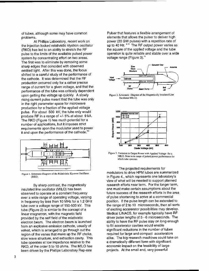
At Phillips Laboratory, recent work on the injection locked relativistic klystron oscillator (RKO) has led to an ability to stretch the RF pulse to the limits of the available pulsed power system by concentrating effort on two areas. The first was to eliminate by removing some sharp edges that coincided with observed emitted light. After this was done, the focus shifted to a careful study of the performance of the cathode. It was determined that the RF production occurred only for a rather precise range of current for a given voltage, and that the performance of the tube was critically dependent upon getting the voltage up quickly. A slowly rising current pulse meant that the tube was only in the right parameter space for microwave production for a fraction of the applied voltage pulse. For about 500 kV, the tube only would produce RF in a range of +/- 5% at about 9 kA. The RKO (Figure 1) has much potential for a number of applications, but it imposes strict requirements upon the modulator used to power it and upon the performance of the cathode.3,9
Figure 1. Schematic Diagram of the Relativistic Klystron Oscillator (RKO).
By sharp contrast, the magnetically insulated line oscillator (MILO) has been observed to operate at a constant frequency over a wide range of operating voltage, varying in frequency by less than 10 MHz for a 1.2 GHz tube over a voltage range of 150-500 kV. This tube (Figure 2) is similar to the concept of a linear magnetron, with the magnetic field provided by the self field of the relativistic electron beam. The electron beam is launched from an explosive emission cathode, usually of velvet, which is arranged to go through out the region of the vanes that make up the RF choke, slow wave structure, and extraction cavity. This tube operates at low impedance relative to the RKO, of the order 5 to 10 ohms. The MILO has been driven by the Phillips Laboratory Rep-rate
Pulser that features a flexible arrangement of elements that allows the pulser to deliver high power (20 GW pulses) with a repetition rate of up to 40 Hz. 9,1° The RF output power varies as the square of the applied voltage and the tube operation is quite reliable and stable over a wide voltage range (Figure 3).11
BdractorGap
Input Voltage
Figure 2. Schematic Diagram of the Magnetically Insulated Line Oscillator MILO).
1200
i 1000
Extractor VIM LO. <CSI) -V-17.14 -*-ia-4a
/ <*■
>ut P
ow
er
3
O
C
) /
/* 3 o ^
//
0 ^ ^
200 300 400 500 Diode Voltage (kV)
Figure 3. Variation in Output Power with Applied Voltage for a MILO. Note wide range of pulsed power performance for which tube operates.
The projected requirements for modulators to drive HPM tubes are summarized in Figure 4., which represents one laboratory's view of what will be needed to support planned research efforts near term. For the longer term, one must make certain assumptions about the future success of the research efforts in the area of pulse shortening to arrive at a commercial position. If the pulse length can be extended to the range of 2 to 10 microseconds, then all sorts of exciting accelerator possibilities may develop. Medical LINACS, for example typically have RF driver pulse lengths of 5 - 6 microseconds. The ability to have the RF pulse stay on long enough to fill accelerator cavities would enable significant reductions in the number of tubes required for large and compact accelerators alike. The big research machines could take on a dramatically different form with significant economic impact on the feasibility of large projects. At the small end, very powerful
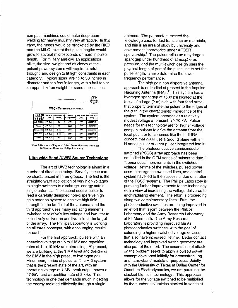
compact machines could make deep beam welding for heavy industry very attractive. In this case, the needs would be bracketed by the RKO and the MILO, except that pulse lengths would grow to several microseconds or more in pulse length. For military and civilian applications alike, the size, weight and efficiency of the pulsed power systems will require careful thought and design to fit tight constraints in each category. Typical sizes are 15 to 30 inches in diameter and ten feet in length, with a half ton or so upper limit on weight for some applications.
WSQN Future Pulser needs
Source Voltage i Impedance (kV) (Ohm)
RaAAcceL 200-500
Pulse Length(ns)
Rep. Rate (Hi)
PulseFonn.1 Req.
Figure 4. Summary of Projected Pulsed Power Modulator Needs for Experiments Planned at Phillips Laboratory.
Ultra-wide Band (UWB) Source Technology
The art of UWB technology is aimed in a number of directions today. Broadly, these can be characterized in three groups. The first is the straightforward application of very high voltages to single switches to discharge energy onto a single antenna. The second uses a pulser to feed a carefully designed non-dispersive high gain antenna system to achieve high field strength in the far field of the antenna, and the third approach uses many radiating elements switched at relatively low voltage and low jitter to collectively deliver an additive field at the target of the array. The Phillips Laboratory is working on all three concepts, with encouraging results for each.12
For the first approach, pulsers with an operating voltage of up to 3 MV and repetition rates of 1 to 10 kHz are interesting. At present, we are building at the 1 MV level and designing for 2 MV in the high pressure hydrogen gas Hindenberg series of pulsers. The H-3 system that is the present state of the art, with an operating voltage of 1 MV, peak output power of 47 GW, and a repetition rate of 2 kHz. This technology is one that demands much in getting the energy radiated efficiently through a single
antenna. The parameters exceed the knowledge base for fast transients on materials, and this is an area of study by university and government laboratories under AFOSR sponsorship.7 The pulser relies on a hydrogen spark gap under hundreds of atmospheres pressure, and the multi-switch design uses the physical length of part of the pulse line to set the pulse length. These determine the lower frequency performance.
The high gain non-dispersive antenna approach is embodied at present in the Impulse Radiating Antenna (IRA)." This system has a hydrogen spark gap at 1500 psi located at the focus of a large (2 m) dish with four feed arms that properly terminate the pulser to the edges of the dish in the characteristic impedance of the system. The system operates at a relatively modest voltage at present, +/- 70 kV. Pulser needs for this technology are for higher voltage compact pulsers to drive the antenna from the focal point, or for schemes like the half-IRA concept that could use a ground plane with an H-series pulser or other pulser integrated into it.
The photoconductive semiconductor switched (PCSS) array approach has been embodied in the GEM series of pulsers to date.12
Tremendous improvements in the switched voltage, lifetime of the switches, pulsed power used to charge the switched lines, and control system have led to the successful demonstration of the PCSS systems. The Phillips Laboratory is pursuing further improvements to the technology with a view of increasing the voltage delivered to each radiating element. The effort is proceeding along two complementary lines. First, the photoconductive switches are being improved in an effort that is joint between the Phillips Laboratory and the Army Research Laboratory at Ft. Monmouth. The Army Research Laboratory is providing improved Ga As photoconductive switches, with the goal of extending to higher switched voltage devices that also have increased lifetime. Better contact technology and improved switch geometry are also part of the effort. The second line of attack on the problem seeks to apply a pulsed power concept developed initially for bremsstrahlung and narrowband modulator purposes. Jointly with the University of Texas at Dallas Center for Quantum Electrodynamics, we are pursuing the stacked blumlein technology . This approach allows for the voltage switched to be multiplied by the number if blumleins stacked in series at
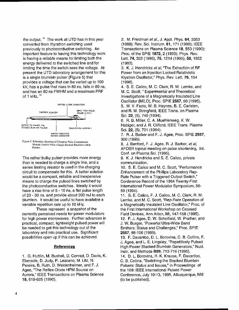
the output.13 The work at UTD has in this year converted from thyratron switching used previously to photoconductive switching. An important feature to having this technology work is having a reliable means for limiting both the energy delivered to the switched line and for limiting the time the switch sees the voltage. At present the UTD laboratory arrangement for this is a single blumlein pulser (Figure 5) that provides a voltage that can be varied up to 100 kV, has a pulse that rises in 80 ns, falls in 80 ns, and has an 80 ns FWHM and a maximum PRF of 1 kHz.14
POTTED OUTER CONDUCTORS
TAPERED BLUMLEIN INPUT FROM PULSE
POWER SUPPLY
OUTPUT TO CHARGE THE
STACKED BLUMLEIN PULSER COMMUTATION ASSEMBLY
KAPT0N SHEATHED CENTER CONDUCTOR
Figure 5. Schematic Drawing of Charging Pulse Compression Module Used to Pulse Charge Stacked Blumlein UWB Pulsers.
The rather bulky pulser provides more energy than is needed to charge a single line, and a series limiting resistor is used in the charging circuit to compensate for this. A better solution would be a compact, reliable and inexpensive means to charge the pulsed lines switched by the photoconductive switches. Ideally it would have a rise time of 5 -10 ns, a flat pulse length of 20 - 30 ns, and provide about 200 mJ to each blumlein. It would be useful to have available a variable repetition rate up to 10 kHz.
These represent a snapshot of the currently perceived needs for power modulators for high power microwaves. Further advances in practical, compact, lightweight pulsed power will be needed to get this technology out of the laboratory and into practical use. Significant possibilities open up if this can be achieved.
References
1. G. Huttlin, M. Bushell, D. Conrad, D. Davis, K. Ebersole, D. Judy, P. Lezcano, M. Litz, N. Pereira, B. Ruth, D. Weidenheimer, and F. J. Agee, "The Reflex-Diode HPM Source on Aurora," IEEE Transactions on Plasma Science 18,618-625(1990).
2. M. Friedman etal., J. Appl. Phys. 64, 3353 (1988); Rev. Sei. Instrum. 61, 171 (1990); IEEE Transactions on Plasma Science 18, 553 (1990); Proc. of the SPIE 1872, 2 (1993); Phys. Rev. Lett. 74, 322 (1995), 75, 1214 (1995), 50, 1922 (1983). 3. K. J. Hendricks et al, "The Extraction of RF Power from an Injection Locked Relativistic Klystron Oscillator," Phys. Rev. Lett. 76,154 (1996). 4. S. E. Calico, M. C. Clark, R. W. Lemke, and M. C. Scott," Experimental and Theoretical Investigations of a Magnetically Insulated Line Oscillator (MILO), Proc. SPIE 2557, 50 (1995). 5. M. V. Fazio, W. B. Haynes, B. E. Carlsten, and R. M. Stringfield, IEEE Trans, on Plasma Sei. 22, (5), 740(1994). 6. R. B. Miller, C. A. Muehlenweg, K. W. Habiger, and J. R. Clifford, IEEE Trans. Plasma Sei. 22, (5), 701 (1994). 7. R. J. Barker and F. J. Agee, Proc. SPIE 2557, 300(1995). 8. J. Benford, F. J. Agee, R. J. Barker, etal, AFOSR topical meeting on pulse shortening, Int. Conf. on Plasma Sei. (1995). 9. K. J. Hendricks and S. E. Calico, private communication. 10. S. E. Calico and M. C. Scott, "Performance Enhancement of the Phillips Laboratory Rep- Rate Pulser with a Triggered Output Switch," Conference Record of the 1994 Twenty-First International Power Modulator Symposium, 56- 59(1994). 11. S. E. Calico, F. J. Calico, M. C. Clark, R. M. Lemke, and M. C. Scott, "Rep-Rate Operation of a Magnetically Insulated Line Oscillator," Proc. of the First International Workshop on Crossed Field Devices, Ann Arbor, Ml, 147-158 (1995). 12. F. J. Agee, D. W. Scholfield, W. Prather, and J. W. Burger, "Powerful Ultra-Wide Band Emitters: Status and Challenges," Proc. SPIE 2557,98-106(1995). 13. F. Davanloo, D. L. Borovina, C. B. Collins, F. J. Agee, and L. E. Lingsley, "Repetitively Pulsed High Power Stacked Blumlein Generators," Nucl. Instr. and Methods B99, 713-716 (1995). 14. D. L. Borovina, R. K. Krause, F. Davanloo, C. B. Collins, "Switching the Stacked Blumlein Pulsers: Status and Issues," in Proceedings of the 10th IEEE International Pulsed Power Conference, July 10-13,1995, Albuquerque, NM (to be published).
The Role of Pulsed Power Accelerator Technology in Science-Based Stockpile Stewardship
Juan J. Ramirez Sandia National Laboratories
Albuquerque, New Mexico, 87185-1178
ABSTRACT
The end of the cold war with the Soviet Union, the rise of nationalism, regionalism, and terrorism, the spread of weapons of mass destruction, and the globalization of national economies represent historical changes that have led to a major restructuring of the nation's nuclear weapon program. Nuclear weapons remain a key element of the nation's strategic deterrent policy although their number in the stockpile is being reduced dramatically. On August 11, 1995, the President announced his decision to seek a zero-yield comprehensive test ban treaty. Prior to his announcement, the President was assured by the Department of Energy Secretary and the directors of the three nuclear weapons laboratories that a robust Science-Based Stockpile Stewardship program could be established to maintain a sufficiently high level of confidence in the safety and reliability of the nation's nuclear stockpile. This paper describes the major pulsed power accelerator initiatives within the national Science-Based Stockpile Stewardship program.
I. INTRODUCTION
The dramatic collapse of the Soviet Union has led to fundamental changes in the geopolitical environment that had been in place since the second world war. No longer do we have two major superpowers confronting each other across the globe; armed with tens of thousands of nuclear weapons targeted on each other. Although nuclear weapons remain a key element of the nation's strategic deterrent policy, their number in the enduring stockpile is being reduced dramatically. Last year, the President committed this nation to pursuing a zero-yield comprehensive test ban treaty (CTBT) to be signed by the end of 1996, and declared that underground nuclear tests (UGTs) would resume only under a "supreme national interest" clause in the treaty. This would only be done if the Department of Energy (DOE) and the Department of Defense (DoD) jointly certify that they lacked confidence in a vital type of weapon in the nuclear stockpile. Maintaining a safe and secure stockpile has been an exceedingly demanding job that in the past relied heavily on underground nuclear testing. Prior to his announcement, the President was assured by the Department of Energy Secretary and the directors of the three nuclear weapons laboratories that a robust Science-Based Stockpile Stewardship (SBSS) program could be established to maintain a sufficiently high level
confidence in the safety and reliability of the stockpile. The approach being taken is to develop a more comprehensive understanding of relevant nuclear science and technology; using an ensemble of advanced laboratory experimental facilities. These facilities, together with the advanced scientific computing initiative, will provide the knowledge-base necessary to certify the safety and reliability of the stockpile.
II. PULSED POWER ACCELERATOR CAPABILITIES
Pulsed Power Accelerator Technology has its origins in the 1950s and 1960s, and over the past decades has matured into a flexible and robust discipline. The major advantage provided by pulsed power is its ability to generate and deliver very high energy and very high power pulses at low cost and high efficiency. The principal applications of pulsed power systems within the DOE Defense Programs include the areas of weapon physics, radiation effects simulation and testing, and inertial confinement fusion (ICF).
The development of pulsed power within the DOE has been driven by the applications to defense programs. An early application was to x-ray radiography of very dense imploding systems [1]. In the late 1960s a number of high power bremmstrahlung sources were built to test the effects of radiation from a nuclear weapon on electronic systems and subsystems. This work was performed at a number of DOE and DoD laboratories, as well as in industry [2]. Success in these areas led to the establishment of the particle beam fusion program in the early 1970s [3]. This program applies the low-cost, high- efficiency promise of pulsed power to the longer-term goals of the national ICF program; i.e., gain with stand- off and Inertial Fusion Energy. The ICF program stimulated the development of modular, high-current, high-voltage, multi-terawatt pulsed power generators which then led to the development of a new generation of radiation effects simulators in the mid 1980s. Saturn [4] and Hermes III [5] were constructed at Sandia as part of an effort to build a more robust radiation effects science and simulation program, and to reduce its dependence on UGTs. The advent of fast pulsed power accelerators also resulted in major advances in intense pulsed x-ray sources using magnetically driven plasma implosions; i.e., z-pinches [6]. These facilities enable high energy plasma implosions driven to completion before instabilities can grow to an amplitude sufficiently large to destroy the quality of the implosion. Saturn can
0-7803-3076-5/96/S5.00 © 1996 IEEE
generate 300-500 kJ pulses of x-rays in this mode. The Particle Beam Fusion Accelerator-ll (PBFA-II) at Sandia is the most powerful pulsed power accelerator today and is being modified to allow z-pinch experiments [7]. The conversion to the z-pinch mode will be completed this summer and should produce four times the x-ray power and energy provided by Saturn. The X-1 is a new initiative that will extend this x-ray source capability by another factor of four. Atlas is a high energy density physics research facility being built at Los Alamos National Laboratory (LANL) [8]. It also utilizes the magnetic forces in a z-pinch to achieve very high pressures in an imploding heavy cylindrical liner. Atlas is different in that it uses pulses several microseconds long to drive the implosion.
As indicated earlier, even prior to the moratorium on underground nuclear testing, the DOE weapons laboratories had already started to move away from heavy reliance on UGTs to maintain a safe and reliable stockpile. Both Los Alamos and Lawrence Livermore National Laboratory (LLNL) utilize pulsed-power-driven x-ray radiographic accelerator facilities to support their SBSS programs. The Dual-Axis Hydrodynamics Radiographic Test (DARHT) is a new facility being built at LANL [9]. The DOE has initiated plans for an advanced radiographic hydrotest facility (AHF) to further improve the capabilities provided by DARHT, PHERMEX and the single-axis FXR accelerator facility [10] at LLNL.
accelerator consists of a 4 MeV injector, plus sixty-four 250 keV post-acceleration stages. The key issue for DARHT is the ability to first generate a very high quality beam at the injector and then to retain the beam quality- -by controlling the growth of various beam instabilities- as it propagates through the sixty-four post acceleration stages. LANL has successfully completed the Integrated Test Stand (ITS) experiment consisting of an injector and four post-acceleration stages [11]. The DARHT design is an upgrade based on the experience acquired from the Advanced Test Accelerator (ATA) and the Experimental Test Accelerator (ETA-II) at LLNL [12]. Results from ITS, together with end-to-end system modeling, indicate that DARHT should achieve the desired beam parameters when extended to the full complement of post-acceleration stages. The DARHT accelerator has been funded by DOE and Congress. Construction of the first arm is ongoing; design of DARHT's second arm, with possible performance upgrade to generate four successive electron beam pulses with ~250ns spacing, will begin in fiscal year 1998.
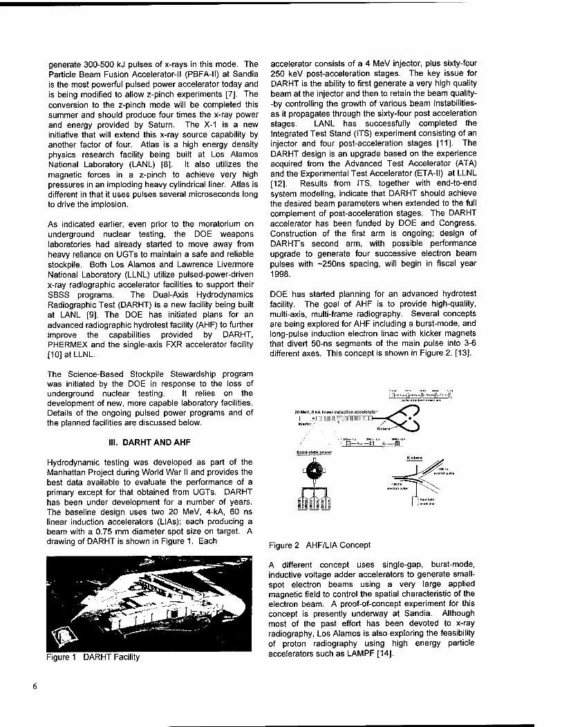
DOE has started planning for an advanced hydrotest facility. The goal of AHF is to provide high-quality, multi-axis, multi-frame radiography. Several concepts are being explored for AHF including a burst-mode, and long-pulse induction electron linac with kicker magnets that divert 50-ns segments of the main pulse into 3-6 different axes. This concept is shown in Figure 2. [13].
The Science-Based Stockpile Stewardship program was initiated by the DOE in response to the loss of underground nuclear testing. It relies on the development of new, more capable laboratory facilities. Details of the ongoing pulsed power programs and of the planned facilities are discussed below.
III. DARHT AND AHF
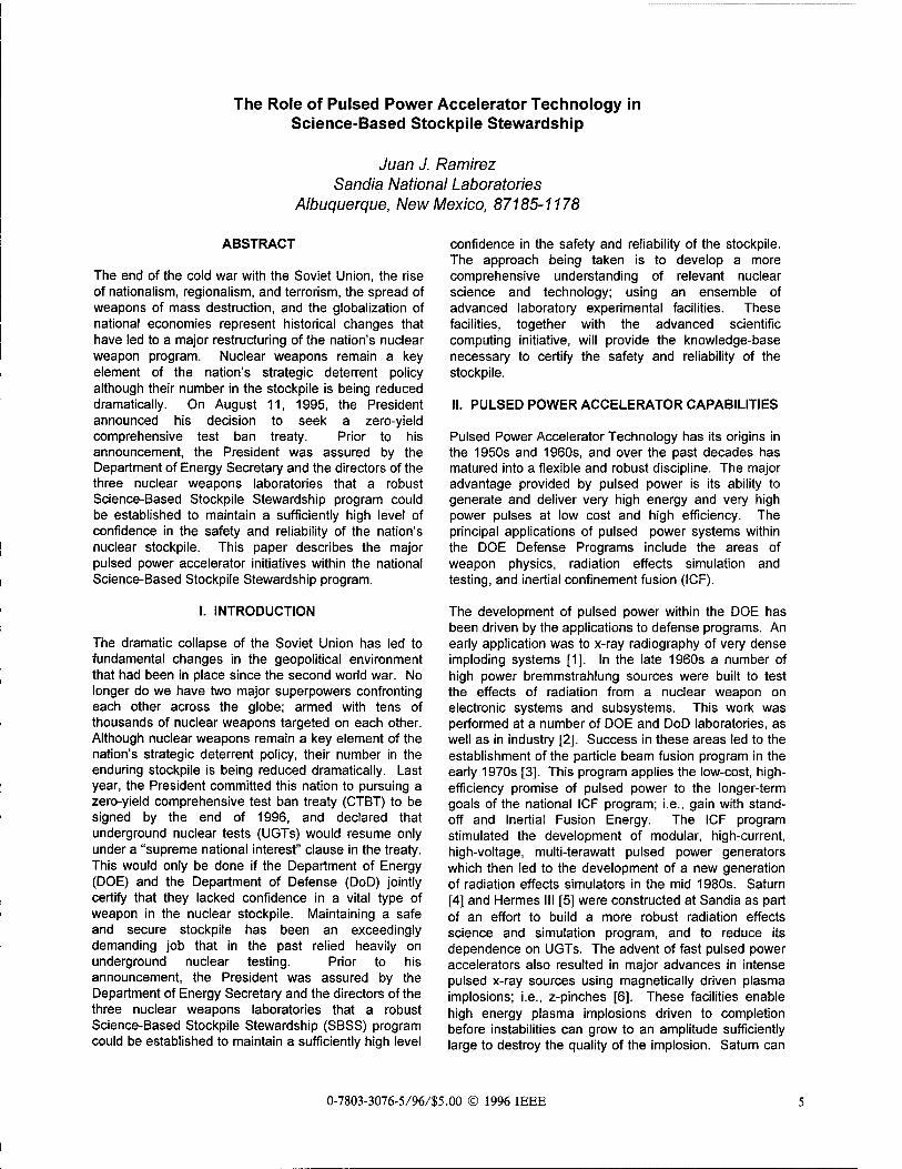
Hydrodynamic testing was developed as part of the Manhattan Project during World War II and provides the best data available to evaluate the performance of a primary except for that obtained from UGTs. DARHT has been under development for a number of years. The baseline design uses two 20 MeV, 4-kA, 60 ns linear induction accelerators (LIAs); each producing a beam with a 0.75 mm diameter spot size on target. A drawing of DARHT is shown in Figure 1. Each
pulw structure w eoeh orm
20 MeV, 6 kA linear induction accelerator
I .wfTnnn]}HrjiniimmL„_. . Injector '. ' /
Kieker
El-*--.fl.. fl_a Solid-state power
Figure 1 DARHT Facility
Figure 2 AHF/LIA Concept
A different concept uses single-gap, burst-mode, inductive voltage adder accelerators to generate small- spot electron beams using a very large applied magnetic field to control the spatial characteristic of the electron beam. A proof-of-concept experiment for this concept is presently underway at Sandia. Although most of the past effort has been devoted to x-ray radiography, Los Alamos is also exploring the feasibility of proton radiography using high energy particle accelerators such as LAMPF [14].
IV. ATLAS and instabilities in relevant geometry may require sources in excess of 20 MJ.
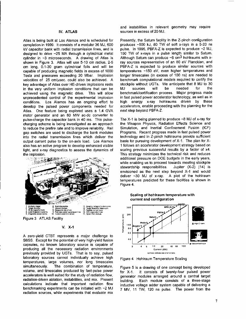
Atlas is being built at Los Alamos and is scheduled for completion in 1999. It consists of a modular 36 MJ, 600 kV capacitor bank with radial transmission lines, and is designed to drive -25 MA through a cylindrical metal cylinder in ~3 microseconds. A drawing of Atlas is shown in Figure 3. Atlas will use 5-10 cm radius, 2-5 cm long, 0.1-30 gram cylindrical foils and will be capable of producing magnetic fields in excess of 1000 Tesla and pressures exceeding 20 Mbar. Implosion velocities of 25 cm/nsec. could also be achieved. A key advantage of Atlas over HE-driven implosions rests in the very uniform implosion conditions that can be achieved using the magnetic drive. This will allow unprecedented control of the experimental implosion conditions. Los Alamos has an ongoing effort to develop the pulsed power components needed for Atlas. One feature being explored uses a 1.4 GVA motor generator and an 80 MW ac-dc converter to pulse-charge the capacitor bank in 40 ms. This pulse- charging scheme is being investigated as an approach to reduce the prefire rate and to improve reliability. Rail gap switches are used to discharge the bank modules into the radial transmission lines which deliver the output current pulse to the on-axis load. Los Alamos also has an active program to develop enhanced visible light, and x-ray diagnostics to assess the dynamics of the implosion.
1 Implosjon target 2- Target chamber 3. 36-MJ capacitor bar* 4. Laser dtegnostic systems 5. Diagnostic screen rooms
6. Axial diagnostics 7. Vacuum pumps 8. Diagnostic line ot site 9. Rat-plate radial transmission line
10. T(ansmission.|ine ballast
11. Imaging radiography darkrooms 12. Target assembly clean room 13. Satelite control room 14. NTS diagnostic trailer 15. Spare Marx module
Figure 3 ATLAS Facility
V. X-1
A zero-yield CTBT represents a major challenge to SBSS. Except for the potential of very high-yield fusion capsules, no known laboratory source is capable of producing all the necessary radiation environments previously provided by UGTs. That is to say, pulsed laboratory sources cannot individually achieve high temperatures, large volumes, nor long timescales simultaneously. The combination of temperature, volume, and timescales produced by fast-pulse power accelerators is well suited for the study of radiation flow, radiation-driven ablation, instabilities, and mix. Present calculations indicate that important radiation flow benchmarking experiments can be initiated with ~2 MJ radiation sources, while experiments that evaluate mix
Presently, the Saturn facility in the Z-pinch configuration produces -500 kJ, 80 TW of soft x-rays in a 5-20 ns pulse. In 1996, PBFA-Z is expected to produce -2 MJ, 150 TW of x-rays in a pulse length similar to Saturn. Although Saturn can produce -6 cm3 hohlraums with x- ray sources representative of an 80 eV Planckian, and PBFA-Z is expected to produce similar sources with temperatures -150 eV, even higher temperatures and longer timescales (in excess of 100 ns) are needed to benchmark computational models required to certify the stockpile without UGTs. We anticipate that 8 MJ to 30 MJ sources will be needed for the benchmark/certification process. Major progress made in fast pulsed power accelerator technology, as well as in high energy x-ray hohlraums driven by these accelerators, enable proceeding with the planning for the next step beyond PBFA-Z.
The X-1 is being planned to produce -8 MJ of x-ray for the Weapon Physics, Radiation Effects Science and Simulation, and Inertial Confinement Fusion (ICF) Programs. Recent progress made in fast pulsed power technology and in Z-pinch hohlraums provide sufficient basis for pursuing development of X-1. The plan for X- 1 follows an accelerator development strategy based on scaling previous successful results by a factor of x4. This strategy minimizes the technical risk and reduces additional pressure on DOE budgets in the early years, while enabling us to proceed towards meeting stockpile stewardship responsibilities. Jupiter (X-2) [14] is envisioned as the next step beyond X-1 and would deliver -30 MJ of x-ray. A plot of the hohlraum temperatures predicted for these facilities is shown in Figure 4.
Scaling of hohlraum temperature with current and configuration
Jupiter
Vaccum hohlnum
2 4 6 10 20 40 60 100
Current (MA)
symbols indicate size ot error bars
Figure 4 Hohlraum Temperature Scaling
Figure 5 is a drawing of one concept being developed for X-1. It consists of twenty-four pulsed power generator modules arranged around a central target building. Each module consists of a three-stage inductive voltage adder system capable of delivering a 7 MV, 11 TW, 120 ns pulse. The power from the
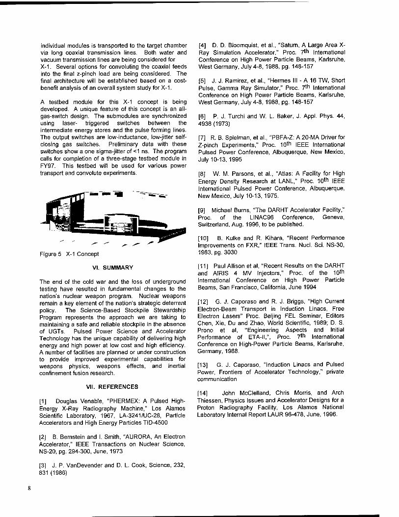
individual modules is transported to the target chamber via long coaxial transmission lines. Both water and vacuum transmission lines are being considered for X-1. Several options for convoluting the coaxial feeds into the final z-pinch load are being considered. The final architecture will be established based on a cost- benefit analysis of an overall system study for X-1.
A testbed module for this X-1 concept is being developed. A unique feature of this concept is an all- gas-switch design. The submodules are synchronized using laser- triggered switches between the intermediate energy stores and the pulse forming lines. The output switches are low-inductance, low-jitter self- closing gas switches. Preliminary data with these switches show a one sigma-jitter of <1 ns. The program calls for completion of a three-stage testbed module in FY97. This testbed will be used for various power transport and convolute experiments.
Figure 5 X-1 Concept
VI. SUMMARY
The end of the cold war and the loss of underground testing have resulted in fundamental changes to the nation's nuclear weapon program. Nuclear weapons remain a key element of the nation's strategic deterrent policy. The Science-Based Stockpile Stewardship Program represents the approach we are taking to maintaining a safe and reliable stockpile in the absence of UGTs. Pulsed Power Science and Accelerator Technology has the unique capability of delivering high energy and high power at low cost and high efficiency. A number of facilities are planned or under construction to provide improved experimental capabilities for weapons physics, weapons effects, and inertial confinement fusion research.
VII. REFERENCES
[1] Douglas Venable, "PHERMEX: A Pulsed High- Energy X-Ray Radiography Machine," Los Alamos Scientific Laboratory, 1967, LA-3241/UC-28, Particle Accelerators and High Energy Particles TID-4500
[2] B. Bernstein and I. Smith, "AURORA, An Electron Accelerator," IEEE Transactions on Nuclear Science, NS-20, pg. 294-300, June, 1973
[3] J. P. VanDevender and D. L. Cook, Science, 232, 831 (1986)
[4] D. D. Bloomquist, et al., "Saturn, A Large Area X- Ray Simulation Accelerator," Proc. 7th International Conference on High Power Particle Beams, Karlsruhe, West Germany, July 4-8, 1988, pg. 148-157
[5] J. J. Ramirez, et al., "Hermes III - A 16 TW, Short Pulse, Gamma Ray Simulator," Proc. 7th International Conference on High Power Particle Beams, Karlsruhe, West Germany, July 4-8, 1988, pg. 148-157
[6] P. J. Turchi and W. 4936(1973)
L. Baker, J. Appl. Phys. 44,
[7] R. B. Spielman, et al., "PBFA-Z: A 20-MA Driver for Z-pinch Experiments," Proc. 10th IEEE International Pulsed Power Conference, Albuquerque, New Mexico, July 10-13, 1995
[8] W. M. Parsons, et al., "Atlas: A Facility for High Energy Density Research at LANL," Proc. 10*n IEEE International Pulsed Power Conference, Albuquerque, New Mexico, July 10-13, 1975.
[9] Michael Burns, "The DARHT Accelerator Facility," Proc. of the LINAC96 Conference, Geneva, Switzerland, Aug. 1996, to be published.
[10] B. Kulke and R. Kihara, "Recent Performance Improvements on FXR," IEEE Trans. Nucl. Sei. NS-30, 1983, pg. 3030
[11] Paul Allison et al, "Recent Results on the DARHT and AIRIS 4 MV Injectors," Proc. of the 10*" International Conference on High Power Particle Beams, San Francisco, California, June 1994
[12] G. J. Caporaso and R. J. Briggs, "High Current Electron-Beam Transport in Induction Linacs, Free Electron Lasers" Proc. Beijing FEL Seminar, Editors Chen, Xie, Du and Zhao, World Scientific, 1989; D. S. Prono et al, "Engineering Aspects and Initial Performance of ETA-II,", Proc. 7th International Conference on High-Power Particle Beams, Karlsruhe, Germany, 1988.
[13] G. J. Caporaso, "Induction Linacs and Pulsed Power, Frontiers of Accelerator Technology," private communication
[14] John McClelland, Chris Morris, and Arch Thiessen, Physics Issues and Accelerator Designs for a Proton Radiography Facility, Los Alamos National Laboratory Internal Report LAUR 96-478, June, 1996.
Space Power Technology
M. Frank Rose
Space Power Institute, 231 Leach Science Center, Auburn University, AL 36849
Abstract
The trends today are toward smaller satellites with increased capability. These two trends place enormous demands on the technology used to power space systems. Typical power sources are nuclear, photovoltaic, and chemical. As the power available on a typical satellite decreases, the use of long pulsed sources becomes more attractive. Technologies such as electrochemical capacitors, pulsed batteries, and flywheels offer the possibility of employing high power subsystems for limited times without undue burden on the spacecraft power train. The state of the art in each of the pulsed storage devices will be discussed and preliminary experiments described which use an electrochemical power source to power a spacecraft propulsion unit such as an arc-jet or Hall effect thruster.
Introduction
Currently, the space shuttle has more electrical power ( - 36 kW) on board than any other US spacecraft. Most satellites currently in orbit are in the few kilowatt range and are solar powered. The exceptions to solar power are the deep space probes which employ radioisotope thermoelectric units to provide power for years independently of position, with respect to the sun.
Since the engineering properties of a high vacuum and space are well documented, it is a legitimate question to ask why there are engineering problems associated with power systems in space. Most satellites are specifically designed for a mission with enough power provided for the mission, and it turns out that power technology is an important constraint on mission time. More capability is desired in spacecraft while-the mass/size of spacecraft are decreasing due to cost of mass to orbit. Usually a smaller spacecraft translates into smaller and more sophisticated technology which is prone to failure. Currently there are several schemes for direct communications which will involve hundreds of smaller satellites in constellations which have power requirements much less than kilowatts but must perform tasks formerly relegated to larger more powerful units.
Electric propulsion is gradually taking the place of gas systems for station keeping. In general, it is difficult to use electric propulsion at power levels less than 500W. This places severe demands on the trend to smaller, less powerful units which might want the
overall efficiency of having electric propulsion on board. Similarly, earth observation and some weather satellites are able to gather and record data at a relatively low power level. The data which can be transmitted to an earth station is determined by the power-bandwidth product. At high power levels, enormous quantities of data can be transmitted in short times. Satellite designers are faced with having to size the power train for the peak demand or resort to pulsed sources for long term storage and short term discharge. Pulsed sources should play a significant role in the trend to smaller, more capable satellites.
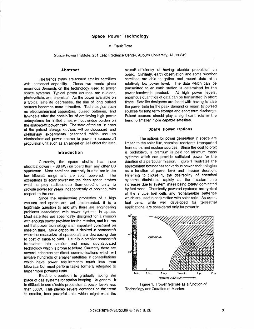
Space Power Options
The options for power generation in space are limited to the solar flux, chemical reactants transported from earth, and nuclear sources. Since the cost to orbit is prohibitive, a premium is paid for minimum mass systems which can provide sufficient power for the duration of a particular mission. Figure 1 illustrates the approximate boundaries for various power technologies as a function of power level and mission duration. Referring to Figure 1, the desirability of chemical systems diminishes rapidly as the mission time increases due to system mass being totally dominated by fuel mass. Chemically powered systems are typical of the shuttle fuel cells and rechargeable batteries which are used in conjunction with solar cells. As such, fuel cells, while well developed for terrestrial applications, are considered only for power in
MISSION DURATION
Figure 1. Power regimes as a function of Technology and Duration of Mission.
0-7803-3076-5/96/S5.00 © 1996 IEEE
transportation systems (shuttle) and specialized short duration missions.
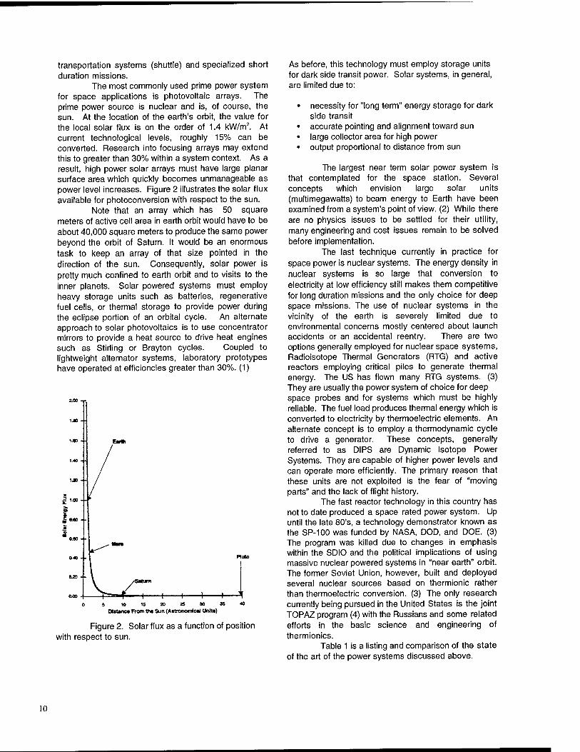
The most commonly used prime power system for space applications is photovoltaic arrays. The prime power source is nuclear and is, of course, the sun. At the location of the earth's orbit, the value for the local solar flux is on the order of 1.4 kW/m2. At current technological levels, roughly 15% can be converted. Research into focusing arrays may extend this to greater than 30% within a system context. As a result, high power solar arrays must have large planar surface area which quickly becomes unmanageable as power level increases. Figure 2 illustrates the solar flux available for photoconversion with respect to the sun.
Note that an array which has 50 square meters of active cell area in earth orbit would have to be about 40,000 square meters to produce the same power beyond the orbit of Saturn. It would be an enormous task to keep an array of that size pointed in the direction of the sun. Consequently, solar power is pretty much confined to earth orbit and to visits to the inner planets. Solar powered systems must employ heavy storage units such as batteries, regenerative fuel cells, or thermal storage to provide power during the eclipse portion of an orbital cycle. An alternate approach to solar photovoltaics is to use concentrator mirrors to provide a heat source to drive heat engines such as Stirling or Brayton cycles. Coupled to lightweight alternator systems, laboratory prototypes have operated at efficiencies greater than 30%. (1)
0 5 » 15 » 2S » 85 «0
Ototenc* From the Sun (Astronomical Units)
Figure 2. Solar flux as a function of position with respect to sun.
As before, this technology must employ storage units for dark side transit power. Solar systems, in general, are limited due to:
• necessity for "long term" energy storage for dark side transit
• accurate pointing and alignment toward sun • large collector area for high power • output proportional to distance from sun
The largest near term solar power system is that contemplated for the space station. Several concepts which envision large solar units (multimegawatts) to beam energy to Earth have been examined from a system's point of view. (2) While there are no physics issues to be settled for their utility, many engineering and cost issues remain to be solved before implementation.
The last technique currently in practice for space power is nuclear systems. The energy density in nuclear systems is so large that conversion to electricity at low efficiency still makes them competitive for long duration missions and the only choice for deep space missions. The use of nuclear systems in the vicinity of the earth is severely limited due to environmental concerns mostly centered about launch accidents or an accidental reentry. There are two options generally employed for nuclear space systems, Radioisotope Thermal Generators (RTG) and active reactors employing critical piles to generate thermal energy. The US has flown many RTG systems. (3) They are usually the power system of choice for deep space probes and for systems which must be highly reliable. The fuel load produces thermal energy which is converted to electricity by thermoelectric elements. An alternate concept is to employ a thermodynamic cycle to drive a generator. These concepts, generally referred to as DIPS are Dynamic Isotope Power Systems. They are capable of higher power levels and can operate more efficiently. The primary reason that these units are not exploited is the fear of "moving parts" and the lack of flight history.
The fast reactor technology in this country has not to date produced a space rated power system. Up until the late 80's, a technology demonstrator known as the SP-100 was funded by NASA, DOD, and DOE. (3) The program was killed due to changes in emphasis within the SDIO and the political implications of using massive nuclear powered systems in "near earth" orbit. The former Soviet Union, however, built and deployed several nuclear sources based on thermionic rather than thermoelectric conversion. (3) The only research currently being pursued in the United States is the joint TOPAZ program (4) with the Russians and some related efforts in the basic science and engineering of thermionics.
Table 1 is a listing and comparison of the state of the art of the power systems discussed above.
10
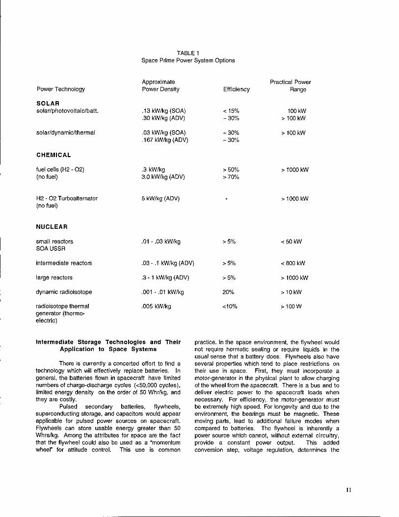
TABLE 1 Space Prime Power System Options
Power Technology Approximate Power Density Efficiency
Practical Power Range
SOLAR solar/photovoltaic/batt. .13kW/kg(S0A)
.30 kW/kg (ADV) <15% ~ 30%
100 kW >100 kW
solar/dynamic/thermal .03 kW/kg (SOA) .167 kW/kg (ADV)
- 30% ~ 30%
>100 kW
CHEMICAL
fuel cells (H2 - 02) (no fuel)
.3 kW/kg 3.0 kW/kg (ADV)
> 50% > 70%
> 1000 kW
H2 - 02 Turboalternator (no fuel)
5 kW/kg (ADV) - > 1000 kW
NUCLEAR
small reactors SOA USSR
.01 - .03 kW/kg >5% <50kW
intermediate reactors .03 - .1 kW/kg (ADV) >5% < 800 kW
large reactors .3 -1 kW/kg (ADV) >5% > 1000 kW
dynamic radioisotope .001 - .01 kW/kg 20% >10kW
radioisotope thermal generator (thermo- electric)
.005 kW/kg <10% >100W
Intermediate Storage Technologies and Their Application to Space Systems
There is currently a concerted effort to find a technology which will effectively replace batteries. In general, the batteries flown in spacecraft have limited numbers of charge-discharge cycles (<50,000 cycles), limited energy density on the order of 50 Whr/kg, and they are costly.
Pulsed secondary batteries, flywheels, superconducting storage, and capacitors would appear applicable for pulsed power sources on spacecraft. Flywheels can store usable energy greater than 50 Whrs/kg. Among the attributes for space are the fact that the flywheel could also be used as a "momentum wheel" for attitude control. This use is common
practice. In the space environment, the flywheel would not require hermatic sealing or require liquids in the usual sense that a battery does. Flywheels also have several properties which tend to place restrictions on their use in space. First, they must incorporate a motor-generator in the physical plant to allow charging of the wheel from the spacecraft. There is a bus and to deliver electric power to the spacecraft loads when necessary. For efficiency, the motor-generator must be extremely high speed. For longevity and due to the environment, the bearings must be magnetic. These moving parts, lead to additional failure modes when compared to batteries. The flywheel is inherently a power source which cannot, without external circuitry, provide a constant power output. This added conversion step, voltage regulation, determines the
11

"depth of discharge" of the wheel while introducing a further loss mechanism associated with the regulator. The regulator adds mass to the spacecraft which otherwise could be used as payload. In spite of these difficulties, flywheels appear promising for replacing batteries in future spacecraft. They do not appear promising as a pulsed source to augment the standard power train for the spacecraft. Reis and Kirk (5) have designed a unit for such an application which would store approximately 65 Whrs/kg when operated between 80,000 and 40,000 rpm. Power density should be in excess of 100 W/kg. At present, this technology is relatively immature.
The need for cryogens effectively eliminates the use of Superconducting Magnetic Energy Storage (SMES) units from application within local spacecraft. For deep space applications, it may be possible to eliminate the need for cryogens since beyond Saturn, the local temperature is less than 20 K and the solar constant as shown in Figure 2 is insufficient to provide surface heating. In that scenario, inductive stores might be applicable.
There are two technologies which might be used to augment the conventional power train for pulsed duty at power levels factors of 2-10 times that available on the power bus. A potential energetic and power dense pulsed battery for space applications is the thin film versions of the classical lead-acid cells which have been in use for a century. Bolder Technologies Corporation, Boulder, Colorado, has constructed cells with specific power levels in excess of 5 kW/kg and 16 kW/liter. The company claims that their unique thin film metal cells have produced batteries with the lowest internal impedance of any known rechargeable battery chemistry. The company claims that the batteries are capable of 300 deep charge-discharge cycles and over 5000 partial charge- discharge cycles. Obviously for space applications, the cycle life would have to be extended by a factor of 100. Hence, except for specialty short duration missions, the ability to use pulsed batteries is limited.
The interface between a conductor and a liquid electrolyte forms a layer capable of storing charge. Other researchers have discovered that pseudocapacitance in ruthenium oxide could also store enormous charge when compared with conventional capacitors. Subsequent research has led to the development of capacitor technology which has high power and energy density. While the energy density is less than most battery technologies, the power density is factors of 10 - 50 greater than that of "conventional" batteries and as good as or better than the pulsed battery above. A combination of prime power in the form of a solar array or solar array-battery and a chemical double layer capacitor form a unique combination of high peak power and average power system for many space and terrestrial applications.
Supercapacitors are "designer" devices which can be custom tailored both electrically and geometrically to a particular task.
Table 2 lists a representative sampling of the technologies funded by many agencies and by private industry for a variety of applications. Two units suitable for large energy storage are available from Panasonic in 1500 F and 470 F units, both rated at 2.3 V. The 470 F unit can be successfully operated at 3.0 V with some decrease in lifetime. Due to the voltage dependence of the double layer thickness, the capacitance at 3.0 V is greater than 500 F with an equivalent series resistance of a few milliohms. Under the operating conditions described above, these units have a maximum energy storage density of 4.6 kJ/kg. These units can function with minimal degradation for 600,000 charge-discharge cycles at a charge voltage 30% over the manufacturer's specification. This is approaching the range of interest for space applications.
Electric Propulsion for Spacecraft
In 1929, Hermann Oberth published his ideas on electric propulsion in his famous book on rocketry and space travel. (6) Electric propulsion is just beginning to be introduced on commercial satellites for station keeping. There are numerous studies showing the benefits for orbit raising and for interplanetary missions. Electric propulsion is accomplished by the acceleration of gases by electrical heating and/or by JXB forces acting on a conducting plasma made up of the gas constituents. The most prominent techniques can be grouped into electrothermal propulsion, electrostatic propulsion and electromagnetic propulsion. For electromagnetic and electrothermal thrusters, it is difficult to obtain stable operation at low power levels. The obvious alternative is to operate a high power thruster in a pulsed mode to achieve the desired average power. In a recent paper, Rose, Hrbud, and Merryman (7) examined two modes for achieving pulsed operation of an arcjet thruster. For a CDL capacitor bank operating through a conventional power conditioning unit, they showed that average power levels of a few hundred watts could be achieved with a CDL power pack with a mass of a few kilograms.
Based upon test data, a power pack providing 500 W average power with peaks on the order of 1.5 kW should be able to operate continuously in this mode for at least a million cycles which would translate to roughly two years. This would be sufficient for slow Lunar and Mars transfer. The "modulator" is very simple and consists of a bank made of segments whose charge voltage is that of the spacecraft bus and a simple Marx switching arrangement to apply higher voltages to the thruster.
12
Table 2 Summary of Electrochemical Capacitor Technology.
Name Construction Performance Status
Electrode Material Electrolyte (kJ/kg)
Resistance
(fi-cm2) (W/kg) Volt. (V)
Cap. (F) State of the Art
NEC Supercap FY
carbon sulfuric acid
1.2 45 — 5 2.2 Spec. Sheet
NEC Supercap FE
carbon sulfuric acid
0.03 1.9 — 5 1.5 Spec. Sheet
Panasonic carbon organic 7.9 7 400 3 500-1500 Lab Tests
Evans/Army carbon Ru02(hydrous) (P)
sulfuric acid
0.7 >25
1 <1 >2000
11 5
0.5 5
Spec. Sheet Lab Cells
Seiko Instruments
polyacene polymer
organic 6.8 12 — 5 2.5 Spec. Sheet
Pinnacle Research Institute
mixed oxides (Ru.Ta) Adv. desiqn (P)
sulfuric acid
18 >10,000 100 0.01 Mfr. Testing
Maxwell/ Auburn
carbon/metal composite
KOH organic
6.8 25.0
0.2 1.5
800 2000
1 3
55 13
Lab Cells
Livermore National Lab
aerogel carbon particulate
KOH 3.6 — — 1 35 Lab Cells
Sandia National Lab
synthetic, activated carbon
aqueous 5.0 0.35 1000 1 3.5 Lab Cells
Los Alamos National Lab
conducting polymeron carbon
organic (solid)
36.0- 72.0
Estimated
Technautics Hypercap
anode-Ag cathode-C (P)
solid RbAg4l5
2.0 ohms 3000 0.6 ""
Mfr. Data
(P) Psuedocapacitance
Hrbud (8) has also used the same technology to power the Hall effect thrusters developed in the former Soviet Union.
Batteries which are used in space technology have power densities between 50 and 200 W/kg. Batteries have limited charge-discharge cycle life. Using the above numbers for power density, a battery capable of providing 1.5 kW needed by a thruster would weigh between 10 and 38 kg. It could also operate at the peak power level continuously. The equivalent weight for a space rated capacitor would be on the order of 2 kg but could provide the needed power for a limited time. It, of course, would need a power train sized to allow 500W average power available for propulsion. The best capacitor technology listed in Table 2 would reduce the capacitor mass even further. Note that there is now a weight reduction for the propulsion power of about a factor of 5 or more over that powered solely by batteries sized for the peak power.
There is considerable research within the R&D community to replace hydraulic systems with electrical driven systems where possible. For electric actuation, the motivating factors are increased reliability, reduced environmental impact, reduction in expensive ground
tests and maintenance, reduced costs, and lighter weight. There are a variety of improved electric components, power processors and high energy density-high power density sources emerging from the R&D laboratories which make electric actuation more competitive.
For many actuation applications, the actuation process is pulsed with high peak power requirements but with relatively modest average power levels. The power pulse needed is on the order of seconds which makes the electrochemical capacitor technologies particularly relevant. The most promising options for the power source is a battery-capacitor hybrid. The battery-capacitor hybrid system uses the battery to supply the average power and the capacitor to meet the peak demands and typically results in a smaller, more efficient system. Merryman and Hall (9) have described the construction of an experimental 270-V, 5.34 F capacitor bank system using off-the-shelf, commercial CDL capacitor technology and the evaluation of its ability to perform electrical actuation typical of that needed for the space shuttle thrust vector control. The battery bank used in these tests consisted of 21 deep- cycle, marine lead-acid batteries configured into a
13
270-V system capable of providing up to 400 A. This power pack was not optimum for either energy density or power density but is adequate to demonstrate the technology. The 50 hp actuator used in their tests is the first generation Thrust Vector Control (TVC) prototype designed at NASA Marshall Space Flight Center(10). The system consists of two 25 hp motors, a gear train, roller screw, and two 27 kW analog controllers. The load bench, used to validate the performance of Thrust Vector Control actuators, is capable of operating at loads up to 100,000 Ibf and rates up to 20 in/sec. The CDL-battery pack was tested for no load, 5, 10, and 15 thousand pounds. The battery capacitor hybrid was capable of performing enough actuations to simulate a launch profile. The real benefits of the capacitor bank can be realized when sizing a complete power source to meet the actuation demands. For a battery only system using siiver-zinc technology, the battery requirements are 270 V with a capacity of 80 A-hrs. This battery would weigh approximately 200 kg. With the capacitor bank in a hybrid combination, the battery requirements are reduced to a capacity of 20 A-hrs and would weigh about 45 kg. A state of the art capacitor power pack would weigh about 39 kg. The total power system weight now becomes approximately 84 kg. The battery/capacitor configuration offers a 59% weight savings over the battery only configuration.
Conclusions
The choice of power technology to be employed for a given space mission is very much a function of orbital parameters, lifetime, reliability and the absolute magnitude of the power level required. In general, long duration missions are more demanding. Pulsed power sources may play a significant role in the design of local as well as deep spacecraft as the need for more capability with less energy increases. There appears to be only one option, supercapacitors, which is versatile enough to be used for a variety of missions. As power levels increase, the relationships between thermal management, and the space power system will present a severe challenge to the spacecraft designer probably forcing the use of non-optimum combinations of technology to produce long life spacecraft. At present, there has not been enough research to clearly define the options or to reduce the existing space science data base to engineering guidelines.
References
(1) Shaltens, R.K. and Boyles, R.V., "Update of the 2 kW Solar Dynamic Ground Test Demonstration Program," Proc. 29th IECEC, AIAA-94-4123-CP, pp. 359-365, 1994.
(2) Nansen, R. H., "Wireless Power Transmission, The Key to Solar Power Satellites," Proc. 30th IECEC, IECEC Paper No. AP-78, ASME 1995, pp. 601-612.
(3) Space Nuclear Power Systems, Vol. I-XI, Orbit Book Company, Inc. Malabar, Florida.
(4) Menshikov, et al., "Advanced Development and Using of Space Nuclear Power Systems as a Part of Transport Power Supply Modules for the General Purpose Spacecraft," Proc. Space Technology and Applications International Forum, American Institute of Physics, pp. 1183-1189, 1996.
(5) Reis, D. M. and Kirk, J. A., "Design and Manufacturing for a Composite Multi-Ring Flywheel," Proc. 27th IECEC, pp. 4.43-4.48, vol. 4,1992.
(6) Oberth, H, "Wege zu Raumfahrt", R. Oldenburg KG, Munich, 1929.
(7) Rose, M.F., Hrbud, I., and Merryman, S.A., "Application of Chemical Double Layer Capacitor Technology to Pulsed Electric Thrusters," 30th AIAA/ASME/SAE/ASEE Joint Propulsion Conference, AIAA-94-3304, June 1994.
(8) Hrbud, I., PhD Thesis, To be published.
(9) Merryman, S.A. and Hall, D.K., "Chemical Double- Layer Capacitor Power Source for Electro-mechanical Thrust Vector Control Actuator," AIAA, Journal of Propulsion and Power, Vol. 12, No. 1, pp. 89-94, Jan.- Feb. 1996.
(10) Weir, Rae Ann and Cowan, John R., "Development and Test of Electromechanical Actuators for Thrust Vector Control," NASA Marshall Space Flight Center, AIAA Paper 93-2458, AIAA/SAE/ASME/ASEE 29th Joint Propulsion Conference and Exhibit, June 1993.
Acknowledgments
This work was supported with internal funds provided by the Space Power Institute.
14

Research Issues for New Applications of Power Modulators
Martin A. Gundersen Departments of Electrical Engineering and Physics
University of Southern California Los Angeles, CA 90089-0484
Abstract
Certain fundamental issues are unresolved in the development of components for the power modulators that are required for new applications. Several of these applications are discussed, and required research and development is reviewed. An example in GaAs is presented. It is argued that underlying research supporting the development of high voltage and high repetition rate components, such as switches and capacitors, is needed.
At present, certain limitations to technology required for high power modulators impact the efficiency and applications of such modulators. Potential applications for power modulators include:
Pollution Control Electron Beams Pulsed Lasers Plasma Processing Food Processing High Energy Physics Accelerators Waste Treatment Shock Waves Sterilization Medical Applications Feed Grain Preservation Bacteria in Agriculture Semiconductor Device Processing Metal Surface Treatment Water Purification Various Plasma Applications Smart Power
For example, the requirements for fast rising repetitive pulses limits the use of solid state switches for some of these applications, such as high power pulsed lasers, short-pulse (=<1 |0.sec) light sources, and linear accelerators requiring short pulses. Thus, for example, thyratrons remain the switch of choice for certain linear accelerators because of rise-rate limitations and efficiency issues in modulators based on solid state switches with step-up transformers. Some underlying research issues for modulator components include:
• What are the real limits for solid state switches? • Gas phase switch issues • High repetition rate capacitors
As an example, at present the high energy physics community is considering ideas for advanced accelerators. Several proposals for linear colliders, requiring advanced power modulators, are under study. Some initial proposals, with power modulator requirements, are summarized below in Table I.
TESLA SBLC JLC VLEPP NLC Number of Modulators 604 2800 3000 140 1970
Avg Power (MW)
54 52 32 22 31
Rep Rate 10 50 180 300 180
Pulse 1300 2.8 0.5 0.5 1.2
((isec)
Switch thyristor thyratron thyratron grid-kly thyratron
Table I: Power requirements for conceptual designs for linear collides as of fall 1995. TESLA = TEV superconducting linear accelerator, DESY, Germany; SBLC = S-band Linear Collider, also DESY; JLC = Japan Linear Collider, KEK; VLEPP = Russian collider (Novosibirsk); NLC = Next Linear Collider, SLAC.
Jr
T AMPLIFIERS
1000 100000
BLOCKING VOLTAGE (Volts)
Figure 1. Applications of switches as function of hold off voltage and conduction current.
Application requirements shown in Figure 1 are plotted as a function of required switch hold off voltage and conduction current. These applications are also affected by certain pulse shape issues, including particularly rise-rates for voltage and current.
0-7803-3076-5/96/S5.00 © 1996 IEEE 15
Component problems include: • Magnetic materials • Capacitors
• Much more work is needed, and • More fundamentals - What's the limit?
• Inductors • Switches • Hold-off vs current
Current rate of rise remains an outstanding issue for solid state switches. Speed will improve with better engineering, but the problem actually requires fundamental attention.
To illustrate this, GaAs is an attractive switch material for several reasons. GaAs electron mobility is high, the material has a large energy gap relative to Si, leading to higher hold-off capability and higher temperature operation, and GaAs has also optoelectronic capability. Thus, GaAs appears to be a very good candidate for high power switching applications. However, GaAs to date has shown certain fundamental limitations for power modulator applications. Specifically, when current densities are above ~50A/cm2, (not a large number for Si), a saturation effect occurs which effectively locks the forward drop to a field >5kV/cm. This affects the device forward drop, because ordinarily a thick insulating blocking region is required for a device with high hold-off voltage. This is illustrated in Figure 2. The on-state behavior is characterized by a forward drop that is close to that expected from the intrinsic transferred-electron effect1, or Gunn-type effect, which must be present in GaAs. The effect causes high forward drop and power dissipation for certain pulsed power switches based in GaAs, and various other direct gap materials.
Several conclusions which are important for pulsed power switching may be drawn. Where scattering is possible to a different conduction band valley with a larger effective mass, there will be a pooling of electrons in a high current, high power device with bulk-like characteristics. Semiconductors that have shown this effect include GaAs, InP, Ge, CdTe, InAs, InSb, ZnSe, and many ternary and quaternary semiconductors. Pulsed power switches2, as distinct from other switches including fast, high voltage switches that transfer small energy, are required to hold off large voltages (>lkV), switch large currents (>lkA), and transfer large pulse energies to a load (greater than several joules). In a typical application, a switch might be used to hold off 25 kV, switch a peak current of about 5-10 kA, and transfer -20 joules to a load such as a laser or klystron. It is often of importance that switches designed for such applications transfer energy efficiently—particularly when high repetition rates are required. For example, a GaAs thyristor with a 100 (xm
base may be expected to have a forward drop > 50V, which will be excessive for high current applications. Similar limitations may be expected for the other materials listed above. Specifically, materials in which the transferred-electron effect can occur will not be good candidates for switching applications where low output impedance is required for the power modulators switch.
■ ■ n—i
r -* *
jfw*S
. 600
. 500
■ 400
. 300 \
■ 200
100
200 400 600
Time (nsec)
Cathode (Au/Ge+Ni contact!
K
n+(1019) emitter lum
p (2.5x10¹⁷) barrier 5nm
semi-insulatinc base 200 um
n (10 17) barrier lum
p+(5xl018) emitter l^m
Anode (Cr+Au contact)
FIGURE 2. Above: Typical profiles of current (the upper curve) and voltage (the lower curve) in a pulse forming line switched with the GaAs opto-thyristor. The device initially conducted ~2.5 A for approximately 350 nsec, then switched to a higher current of ~9 A. In the higher current conduction state, the voltage across the device was high, =100 V. Below: Across section of the GaAs opto- thyristor structure used for this study with a Cr-doped, Bridgman grown, semi-insulating GaAs base layer.
Some new materials are shown in Table II.
MATERIALS FOR RESEARCH AND
DEVELOPMENT BLOCKING VOLTAGE FUSE TIME, OPENING
TIME FORWARD DROP COMMENTS
Silicon Carbld« Potentially high not known, fa at not yat known ilgh tamp (400C), Figure ol naril 80 to 2400 batter than
Diamond ahould b« «xtramaly high
n«/na, fMHlbly fatter
raallzad In »witch rery high temp, Flgura or n«rlt103to108>SI
GaAa davlc.
na/nt linear mod«, axpact low drop
ilgh mobility, high atand- >rt, can Integrated with jptical control
Table II. New materials, with favorable properties, requiring research into high power limitations.
16
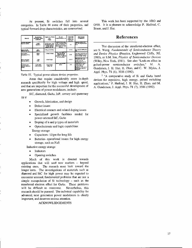
At present, Si switches fall into several categories. In Table HI some of their properties, and typical forward drop characteristics, are summarized.
DEVICE B LOCKING
VOLTAGE, PEAK CURRENT
TURNON/TUBN OFF
TIMES
PULSE CHARACTERISTICS
FORWARD DROP AT 100A/CM* (VOLTS)
ADDITIONAL COMMENTS
ihyriitor(SCfi) 8.5W 80,000 A
10-100 usecr turn oH determined by
circuit, device doeanl turn off
pulM, repetition rat* limited by recovery. Mo*t useful lor high
1.2 lum oH, long recovery llm*
üSässÄ 6kV 4,000 A
5-10|IS/10-1O0M* 1.2-1.5 Can lurn off, difficult to
Field effect irinalator (FET)
Mo* contrail«) ihyrietor(MCT)
-soov 250A
700V 120A
1-IOnsH-IOns UMful lor high
»fficiency. Excellent for fast pulse*
5-10
1.2-1.7
Vary fast, limiled by on ■tal* raaialince, muit •lack lor high voltage
more efficient, with slower turn-off. Developing higher V
n*ulaled git« lipolir translator [IGBT)
1.7kV,600A -1kV,10-50A
<1|ia/ 2-5(1* -20*1« /(i*
-2-5 higher powar, but limilad volltg*. Research underway to lower drop, improve itand-oH.
Table III. Typical power silicon device properties. Areas that require considerably more in-depth
research specifically for high voltage and high speed, and that are important for the successful development of new generations of power modulators, include:
SiC, diamond, GaAs, InP, ternary and quaternary m-v
• Growth, fabrication, and design • Defect issues • Electrical contacts and related doping issues e Specialized growth facilities needed for
power-oriented SiC, GaAs • Doping of n and p types of materials • Optoelectronic and logic capabilities
Energy storage • Capacitors- U/gm for long life • Batteries- operational issues for high energy
storage, such as NaS Inductive energy storage
• Inductors • Opening switches Much of this work is directed towards
applications that will seed new markets - beyond existing ones. The research must look toward the longer term. The investigations of materials such as diamond and SiC for high power may be expected to encounter unusual, fundamental problems that are not a simple extrapolation of Si technology - such as the transferred electron effect for GaAs. These problems will be difficult to overcome. Nevertheless, this research should be pursued. The technical capability for advanced, next generation power modulators is clearly important, and deserves serious attention.
ACKNOWLEDGEMENTS
This work has been supported by the ARO and ONR. It is a pleasure to acknowledge P. Hadizad, C. Braun, and J. Hur.
References
'For discussion of the transferred-electron effect, see S. Wang, Fundamentals of Semiconductor Theory and Device Physics (Prentice, Englewood Cliffs, NJ, 1989), or S.M. Sze, Physics of Semiconductor Devices (Wiley, New York, 1981). See also "Lock-on effect in pulsed-power semiconductor switches," M. A. Gundersen, J. H. Hur, H. Zhao, and C. W. Myles, J. Appl. Phys. 71 (6), 3036 (1992).
2 "A comparative study of Si and GaAs based devices for repetitive, high energy, pulsed switching applications," P. Hadizad, J. H. Hur, H. Zhao, and M. A. Gundersen, J. Appl. Phys. 71 (7), 3586 (1992).
17
Silicon Carbide Power Devices for High Temperature, High Power Density Switching Applications
T. Burke, K. Xie, J. R. Flemish, H. Singh, T. Podlesak U. S. Army Research Laboratory
Fort Monmouth, New Jersey 07703
J. H. Zhao Department of Electrical and Computer Engineering
Rutgers University, P.O. Box 909 Piscataway, New Jersey 08855
Introduction
Silicon Carbide (SiC) has been attracting much attention because of its potential to make high performance power devices with the capability of operating at high temperature. Its avalanche breakdown field is 5 times higher than silicon, its bandgap is approximately three times larger than silicon, and its thermal conductivity is higher than copper, at room temperature.
The wide-bandgap, 2.9 eV for 6H-SiC, allows devices to operate at higher junction temperatures. This capability can be expected to improve cooling efficiency, reduce cooling requirements, improve reliability, and increase current density.
SiC's higher avalanche breakdown field allows higher voltage operation or reduced blocking layer thickness. Devices with thinner blocking layers have lower conduction losses and improved thermal characteristics. The combination of higher thermal conductivity and thinner layers can result in 80x lower die thermal resistance, and a temperature relaxation time 20 times lower than a silicon layer of equal blocking capability. Silicon carbide's higher breakdown field also offers the possibility of extending the fast-switching, lower-loss performance of Schottky rectifiers and MOSFETs to much higher voltages and power levels.
Mature SiC power devices are expected to find use in military systems, utilities, industrial motor drives and actuators, heat pumps, and wherever compact thermal management systems, high operating temperature, or high power density operation is required.
We briefly describe silicon carbide's (SiC) advantages for high power devices, review the state-of the-art in prototype SiC power device performance, and present simulation results and thermal calculations which predict the capability of silicon carbide thyristors in high-power pulse applications. The
simulation also allows a theoretical comparison between high-power silicon carbide thyristors and silicon thyristors in terms of device size, weight and conduction losses. Results suggest that lower voltage devices operated at high current density make best use of silicon carbide's properties and further, that it may be feasible to operate SiC thyristors at current densities above 10 kA/cm2 for millisecond pulsewidths.
We discuss silicon carbide thyristors because MOSFET performance does not, as yet, approach theoretical expectations. Due to conductivity modulation, thyristor-based devices can be expected to have the highest power density at very high power levels. Theoretical evaluations of SiC MOSFETs have been reported*.
Barrier Problems
The most critical and limiting aspect of silicon carbide technology is the material itself. Power devices require low-defect, large-area substrates, and high- quality low-defect uniform epilayers. Although the seeded-sublimation method has been successful in producing large area substrates, up to 2" diameter, the defect level is still too high for commercial production of power devices. The most critical defects are "micropipes" or "micropores". They are "yield- killing" defects which reduce the blocking capability of p-njunctions2.
Cree Research Inc. is a commercial supplier of silicon carbide material. Cree offers a low-micropipe grade of 4H-SiC substrates (1.375 inch diameter) with a specified micropipe defect concentration < 50 cm"2 . To make 1000 A thyristors, micropipe-free areas of at least 1 cm2 are desirable. Cree has identified a number of contributing factors to micropipe formation 3 , and has indicated that there is no apparent theoretical limitation to achieving defect levels below 5/cm2. The lowest defect level reported, averaged over an entire wafer, is 3.5/cm2 . Because of its higher
18 0-7803-3076-5/96/S5.00 © 1996 IEEE
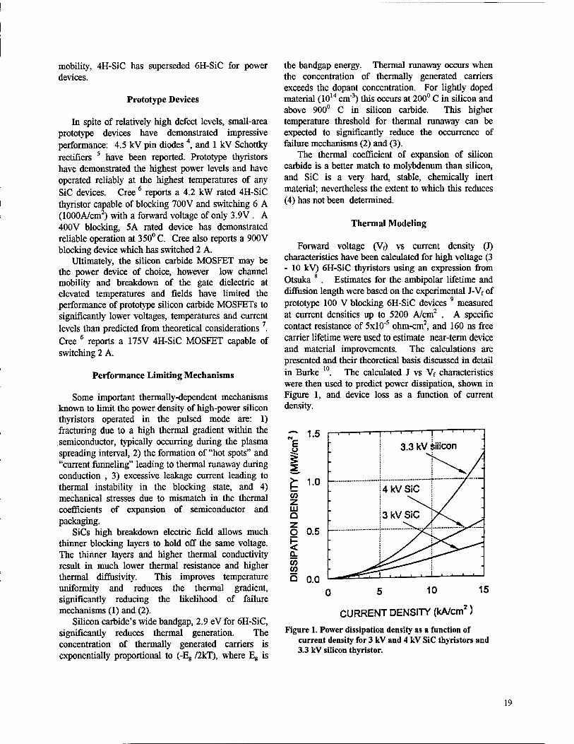
mobility, 4H-SiC has superseded 6H-SiC for power devices.
Prototype Devices
In spite of relatively high defect levels, small-area prototype devices have demonstrated impressive performance: 4.5 kV pin diodes 4, and 1 kV Schottky rectifiers 5 have been reported. Prototype thyristors have demonstrated the highest power levels and have operated reliably at the highest temperatures of any SiC devices. Cree 6 reports a 4.2 kW rated 4H-SiC thyristor capable of blocking 700V and switching 6 A (1000A/cm2) with a forward voltage of only 3.9V . A 400V blocking, 5A rated device has demonstrated reliable operation at 350° C. Cree also reports a 900V blocking device which has switched 2 A.
Ultimately, the silicon carbide MOSFET may be the power device of choice, however low channel mobility and breakdown of the gate dielectric at elevated temperatures and fields have limited the performance of prototype silicon carbide MOSFETs to significantly lower voltages, temperatures and current levels than predicted from theoretical considerations 7. Cree 6 reports a 175V 4H-SiC MOSFET capable of switching 2 A.
Performance Limiting Mechanisms
Some important thermally-dependent mechanisms known to limit the power density of high-power silicon thyristors operated in the pulsed mode are: 1) fracturing due to a high thermal gradient within the semiconductor, typically occurring during the plasma spreading interval, 2) the formation of "hot spots" and "current funneling" leading to thermal runaway during conduction , 3) excessive leakage current leading to thermal instability in the blocking state, and 4) mechanical stresses due to mismatch in the thermal coefficients of expansion of semiconductor and packaging.
SiCs high breakdown electric field allows much thinner blocking layers to hold off the same voltage. The thinner layers and higher thermal conductivity result in much lower thermal resistance and higher thermal diffusivity. This improves temperature uniformity and reduces the thermal gradient, significantly reducing the likelihood of failure mechanisms (1) and (2).
Silicon carbide's wide bandgap, 2.9 eV for 6H-SiC, significantly reduces thermal generation. The concentration of thermally generated carriers is exponentially proportional to (-Eg /2kT), where Eg is
the bandgap energy. Thermal runaway occurs when the concentration of thermally generated carriers exceeds the dopant concentration. For lightly doped material (1014 cm"3) this occurs at 200° C in silicon and above 900° C in silicon carbide. This higher temperature threshold for thermal runaway can be expected to significantly reduce the occurrence of failure mechanisms (2) and (3).
The thermal coefficient of expansion of silicon carbide is a better match to molybdenum than silicon, and SiC is a very hard, stable, chemically inert material; nevertheless the extent to which this reduces (4) has not been determined.
Thermal Modeling
Forward voltage (Vj) vs current density (J) characteristics have been calculated for high voltage (3 - 10 kV) 6H-SiC thyristors using an expression from Otsuka 8 . Estimates for the ambipolar lifetime and diffusion length were based on the experimental J-Vf of prototype 100 V blocking 6H-SiC devices 9 measured at current densities up to 5200 A/cm2 . A specific contact resistance of 5xl0"5 ohm-cm2, and 160 ns free carrier lifetime were used to estimate near-term device and material improvements. The calculations are presented and their theoretical basis discussed in detail in Burke 10. The calculated J vs Vf characteristics were then used to predict power dissipation, shown in Figure 1, and device loss as a function of current density.
'-* 1.5 E u $ 2 >B^
E 1.0 CO z HI a z o U.fa h- < Q. co CO a 0.0
T i i i i
3.3 kV Silicon
0 5 10 15
CURRENT DENSITY (kA/cm2)
Figure 1. Power dissipation density as a function of current density for 3 kV and 4 kV SiC thyristors and 3.3 kV silicon thyristor.
19
The temperature relaxation time of the thin silicon carbide blocking layers (6 us for 4 kV device) is very short, much shorter than that of a comparable silicon device (380 us for a 3.3 kV device). Consequently, steady-state thermal calculations are a reasonable approximation for SiC devices for pulsewidths as short as 100 microseconds. The temperature differential on the SiC die itself can then be estimated from the steady state thermal resistance and the calculated power dissipation density. For a 4kV SiC die operating at 10 kA/cm2 the temperature differential would be 350C. An estimated maximum allowable (transient) junction temperature for SiC of 800° C would then allow a 420° C die-to-ambient temperature differential with which to remove the heat dissipation. A thyristor die operating at 10 kA/cm2 would require a packaging-heat sink with a heat transfer coefficient of 775W/(cm2-°K).
These results indicate the feasibility of operating SiC thyristors at high current densities, perhaps up to 10 kA/cm2, for millisecond pulsewidths. This is approximately four times higher than has been demonstrated by silicon thyristors for millisecond pulsewidths.
The die diameter required to conduct a particular current depends on the allowable current density. Increasing current density by 4 would decrease the required area by 4. The size and weight of the whole device, including packaging, would be reduced by approximately the same factor.
The short (6 \xs) temperature relaxation time for the 4kV silicon carbide thyristor is much less than the expected plasma spreading time for a large thyristor. The plasma spreading time of a large silicon thyristor is on the order of (100 us). Because of its lower mobility, the plasma spreading time of a large silicon carbide thyristor is expected to be longer. This indicates the possibility of significantly removing heat generated during the plasma spreading interval. This would overcome the main limitation to high di/dt operation - fracturing within the semiconductor related to the thermal gradient during the plasma spreading interval. A di/dt improvement of 2.5 times is a reasonable expectation.
Silicon Carbide Benefits and Tradeoffs
Table I shows simulation results comparing a 3.3 kV silicon thyristor and silicon carbide thyristors with different blocking voltages and diameters. Each row of Table 1 shows the area, total volume and total losses for all solid state devices required to make a pulser which can block 20kV and switch 200kA for 3 ms.
All devices in the pulser are the same size and material and have the same blocking voltage and current density ratings. For example, a pulser made using 3.3 kV rated silicon thyristors which can operate at 3kA/cm2
would require a stack of 6 devices to hold off 20 kV and an area of 66.7 cm2 to switch 200kA at a current density of 3kA/cm2. Losses are calculated using the Vf and Power density calculations previously discussed. Percentage losses are calculated based on transfer of approximately 12 MJ to a resistive load by an idealized square 200 kA current pulse 3ms in duration at a voltage of 20kV. Relative loss and relative volume are normalized to the 3.3 kV 66.7 cm2
silicon device, for a clear comparison with silicon. Silicon carbide thyristors with four different ratings
are listed, corresponding to four different regimes of blocking voltage and current density:
Only 2 (high voltage) devices are required for category "C". Unfortunately total loss is highest, and three times that of the silicon device. Similarly only 2 high voltage devices are required for category "B", however losses are still high. Although volume is significantly less than silicon, it is relatively high as well. "A" is a conservative approach, simply matching silicon's current density and blocking voltage capability. However losses are the lowest of all, 23% less than silicon, and total die volume is approximately 1/6 that of silicon. However, the benefit of this lower volume is marginal, because it is due to a thinner die rather than a reduced area.
"D", using low voltage devices operated at high current density, may be the best choice. Losses are only 17% higher than silicon, but devices area is reduced approximately 63%, and the total die volume is about 1/17 . Losses are not particularly critical, but size and weight are. The most important question is whether the devices tolerate the dissipation (losses).
For the high current density low-voltage SiC thyristors; the loss per device is 12.9 kJ. The surface area , 25 cm2 , is approximately 63% less than the silicon devices. However the SiC device is thinner, 58.9 urn, compared with 372 urn for the silicon device. Based on the reduced thickness and higher thermal conductivity of SiC, its thermal resistance is about 14% that of the silicon device, in spite of its smaller area.
Summary
The simulation indicates that by constructing the pulser out of a number of thin lower-voltage rated SiC devices, and operating at a high current density, a size and weight savings of approximately 60% can be obtained at the expense of a 17% increase in losses.
20

Blocking Current No. Voltage Density devices
Table L
Area Loss thickness Total per device (total) Loss %
Volume (Relative) Vol. Loss
kV kA/cm2 cm2 kJ Urn cm3
Silicon 3.3 3.0 6 66.7 11.0 372 0.55% 14.9 1.00 1.00
Silicon Carbide Devices
A 3.3 3.0 6 66.7 8.4 58.9 0.42 % 2.36 0.16 0.77
B 10 3.0 2 66.7 62.6 179 1.04% 2.38 0.16 1.89
C 10 8.0 2 25 101 179 1.69% 0.89 0.06 3.08
D 3.3 8.0 6 25 12.9 58.9 0.64 % 0.88 0.06 1.17
The slightly lower efficiency can most likely be tolerated. More significantly, due to the thinner layers and higher thermal conductivity of the silicon carbide, the thermal resistance of the devices is about 1/7 that of the silicon device. Although the calculated power dissipation density is about 3 times higher, about 172 kJ/cm2, the temperature differential on the die is only 250° C. If the maximum transient junction temperature is 700 C, then up to approximately 420 ° C temperature differential can appear on the case-heat sink to remove the high heat dissipation. A heat transfer coefficient of 410 W/ (cm2 - °K) would be required.
Conclusions
Packaging and cooling requirements, and mismatches in the thermal coefficients of expansion of the silicon carbide and the device packaging, may be the ultimate limitations to high current density operation of SiC thyristors.
Simulation results and thermal analysis indicates that operation at 10 kA/cm2 is feasible with cooling and packaging improvements.
Calculations indicate that by taking advantage of the superior thermal properties of lower voltage SiC devices with thin blocking layers, and operating at 8 kA/cm2, a 60% reduction in device size and weight can be realized at the expense of a 17% increase in losses. Additional calculations show that the temperature
differential on the device die could be as low as 250 ° C, and that removal of the heat dissipation is feasible.
REFERENCES
[1] Bhatnagar, M. and B.J. Baliga, "Comparison of6H-SiC, 3C-SiC, and Si for Power Devices," IEEE Trans, on Electr. Dev., (40), pp. 645, 1993.
[2] Neudeck, P.G., and J. A Powell, "Performance Limiting Micropipe Defects in Silicon Carbide Wafers," IEEE Electron Dev. Lett., 15, pp. 63-65, 1994.
[3] Tsvetkov.V.F. S.T. Allen, H.S. Kong and C.H. Carter, Jr., "Recent Progress in SiC Crystal Growth," Intn'l. Conf. on SiC and Related Material," Kyoto, Japan, Sept. 1995.
[4] Kordina, O., J.P. Bergman, A. Henry, E. Janzen, S. Savage, J. Andre, L.P. Ramberg, U. Lindefelt, W. Hermansson, and K. Bergman, "A 4.5 kV 6H-Silicon Carbides Rectifier,"/4ppA Phys. Lett., (67), p. 1561,1995.
[5] Kimoto, T., T. Urushidani, S. Kobayashi, and H. Matsunami, "High-Voltage (>lkV) SiC Schottky Barrier Diodes with Low On- Resislances," IEEE Electron Dev. Lett., (14), p. 548,1995.
[6] Palmour, J.W.,R. Singh, L. A Lipkin, and D. G. Waltz, "4H- Silicon Carbide High Temperature Power Devices," Trans, of Third Intn'l. High Temperature Electronics Conference, vol. 2, pp. XVI-9, June 9,1996.
[7] B. J. Baliga, "Critical nature of Oxide/Interface quality for SiC Power Devices," Microelectronic Engineering 28, p. 177-184, 1995.
[8] Otsuka, M., Proceedings of the IEEE, vol. 55, #8, p. 1400-1408, Aug. 1967.
[9] Xie, K., J.H. Zhao, J.R. Flemish, T. Burke, W.R Buchwald, G. Lorenzo, and H. Singh, "A high-current and high-temperature 6H- SiC thyristor," IEEE Electron Dev. Lett., vol. 17, no. 3, p. 142- 144, March 1996.
[10] Burke, T., Xie, K, Singh, H., Podlesak, T.,Flemish, J., Carter, J., Schneider, S., Zhao, J., "Silicon Carbide Thyristors for Electric Guns," accepted for pub., IEEE Trans, on Magnetics.
21
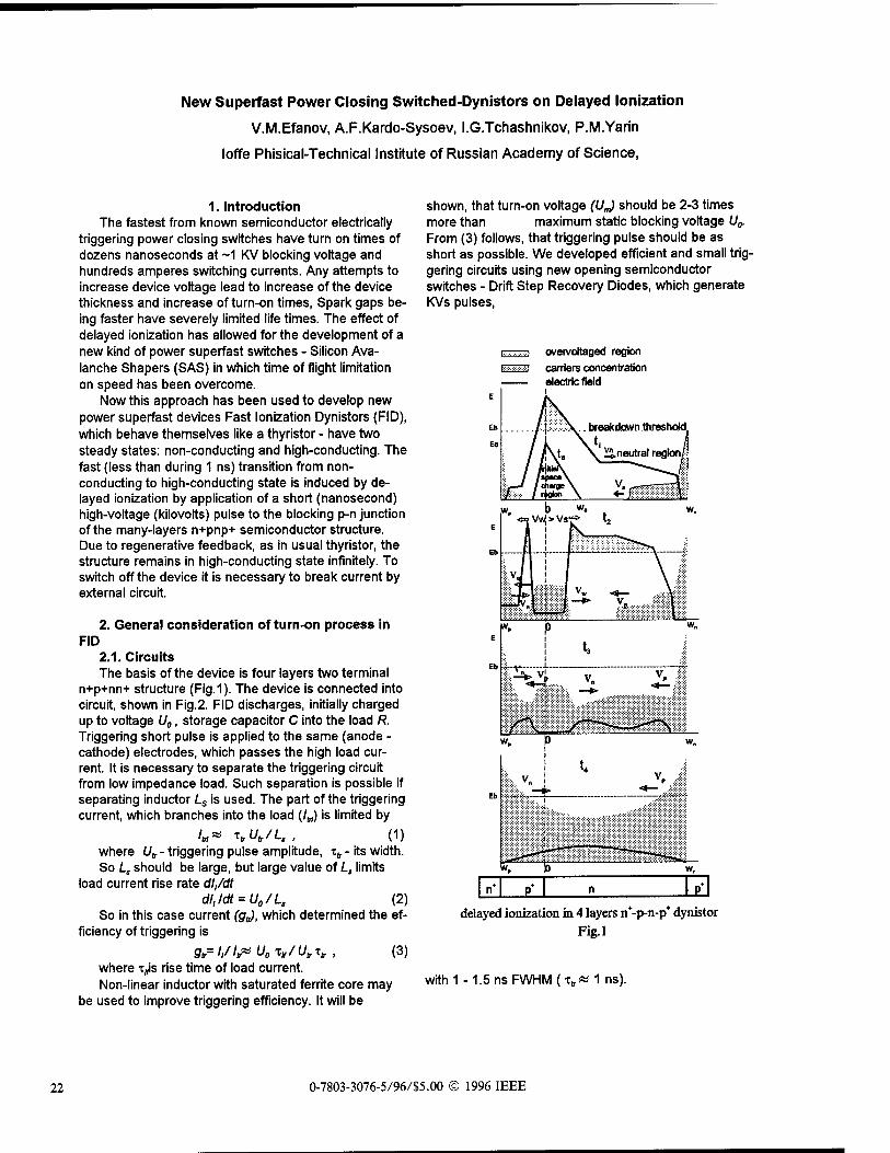
New Superfast Power Closing Switched-Dynistors on Delayed lonization
V.M.Efanov, A.F.Kardo-Sysoev, I.G.Tchashnikov, P.M.Yarin
loffe Phisical-Technical Institute of Russian Academy of Science,
1. Introduction The fastest from known semiconductor electrically
triggering power closing switches have turn on times of dozens nanoseconds at ~1 KV blocking voltage and hundreds amperes switching currents. Any attempts to increase device voltage lead to increase of the device thickness and increase of turn-on times, Spark gaps be- ing faster have severely limited life times. The effect of delayed ionization has allowed for the development of a new kind of power superfast switches - Silicon Ava- lanche Shapers (SAS) in which time of flight limitation on speed has been overcome.
Now this approach has been used to develop new power superfast devices Fast lonization Dynistors (FID), which behave themselves like a thyristor - have two steady states: non-conducting and high-conducting. The fast (less than during 1 ns) transition from non- conducting to high-conducting state is induced by de- layed ionization by application of a short (nanosecond) high-voltage (kilovolts) pulse to the blocking p-n junction of the many-layers n+pnp+ semiconductor structure. Due to regenerative feedback, as in usual thyristor, the structure remains in high-conducting state infinitely. To switch off the device it is necessary to break current by external circuit.
2. General consideration of turn-on process in FID
2.1. Circuits The basis of the device is four layers two terminal
n+p+nn+ structure (Fig.1). The device is connected into circuit, shown in Fig.2. FID discharges, initially charged up to voltage U0, storage capacitor C into the load R. Triggering short pulse is applied to the same (anode - cathode) electrodes, which passes the high load cur- rent. It is necessary to separate the triggering circuit from low impedance load. Such separation is possible if separating inductor Ls is used. The part of the triggering current, which branches into the load (/w) is limited by
/„» x*Ut/L.. (1) where U^ - triggering pulse amplitude, z„ - its width. So Ls should be large, but large value of Lt limits
load current rise rate dl/dt dl,/dt = U0/L, (2)
So in this case current (g„), which determined the ef- ficiency of triggering is
gfl/l,pU0ir/Utxt, (3) where T„is rise time of load current. Non-linear inductor with saturated ferrite core may
be used to improve triggering efficiency. It will be
shown, that turn-on voltage (1/J should be 2-3 times more than maximum static blocking voltage U0. From (3) follows, that triggering pulse should be as short as possible. We developed efficient and small trig- gering circuits using new opening semiconductor switches - Drift Step Recovery Diodes, which generate KVs pulses,
i :m.:.i overvoltaged region
carriers concentration electric field
«a w„
fl ! 1 i J. ' -i
4J> %m
i ti i
w„
;2H- -5. <£..
w. P w„
n* P* n 1 P*
delayed ionization in 4 layers n*-p-n-p* dynistor Fig.l
with 1 - 1.5 ns FWHM (t,» 1 ns).
22 0-7803-3076-5/96/S5.00 © 1996 IEEE
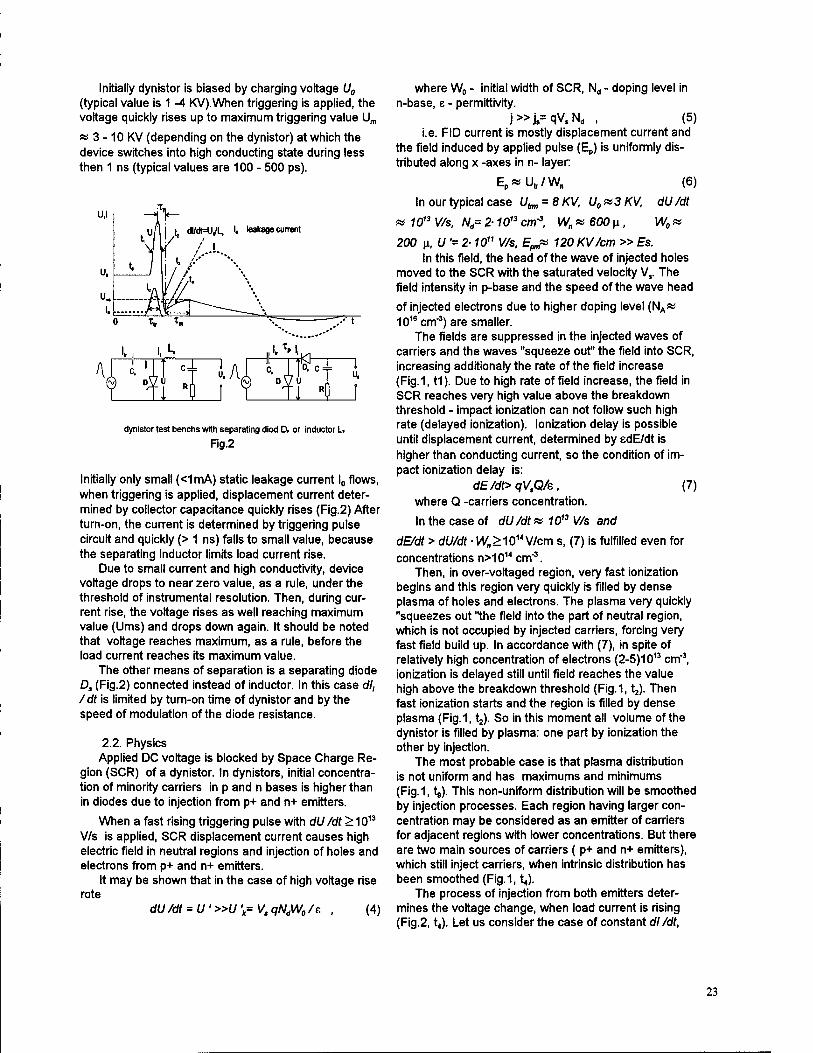
Initially dynistor is biased by charging voltage UB
(typical value is 1 -4 KV).When triggering is applied, the voltage quickly rises up to maximum triggering value Um
« 3 -10 KV (depending on the dynistor) at which the device switches into high conducting state during less then 1 ns (typical values are 100 - 500 ps).
current
t„ Vm
■M. "■> ,I.M Ö- AjrriiPriAraF D\ li
T~l M D V u
dynistor test benchs with separating diod Di or inductor L.
Fig.2
Initially only small (<1mA) static leakage current l„ flows, when triggering is applied, displacement current deter- mined by collector capacitance quickly rises (Fig.2) After turn-on, the current is determined by triggering pulse circuit and quickly (> 1 ns) falls to small value, because the separating inductor limits load current rise.
Due to small current and high conductivity, device voltage drops to near zero value, as a rule, under the threshold of instrumental resolution. Then, during cur- rent rise, the voltage rises as well reaching maximum value (Urns) and drops down again. It should be noted that voltage reaches maximum, as a rule, before the load current reaches its maximum value.
The other means of separation is a separating diode D, (Fig.2) connected instead of inductor. In this case o7, /dt is limited by turn-on time of dynistor and by the speed of modulation of the diode resistance.
2.2. Physics Applied DC voltage is blocked by Space Charge Re-
gion (SCR) of a dynistor. In dynistors, initial concentra- tion of minority carriers in p and n bases is higher than in diodes due to injection from p+ and n+ emitters.
When a fast rising triggering pulse with dU/dt >1013
V/s is applied, SCR displacement current causes high electric field in neutral regions and injection of holes and electrons from p+ and n+ emitters.
It may be shown that in the case of high voltage rise rote
dU/dt = U'»U'k=V,qNJA/0/z , (4)
where W0 - initial width of SCR, Nd - doping level in n-base, e - permittivity.
J»J,= qV,Nd , (5) i.e. FID current is mostly displacement current and
the field induced by applied pulse (Ep) is uniformly dis- tributed along x -axes in n- layer:
E.*Ut/W. (6)
In our typical case U^^BKV, U0&3KV, dU/dt
« 10" V/s, N„= 2-1013 crrf3, W„« 600 u, W0»
200 u, U '= 2-10" V/s, E^ 120 KV/cm » Es. In this field, the head of the wave of injected holes
moved to the SCR with the saturated velocity Vs. The field intensity in p-base and the speed of the wave head
of injected electrons due to higher doping level (NA« 1016cm"3)are smaller.
The fields are suppressed in the injected waves of carriers and the waves "squeeze out"' the field into SCR, increasing additionaly the rate of the field increase (Fig.1, t1). Due to high rate of field increase, the field in SCR reaches very high value above the breakdown threshold - impact ionization can not follow such high rate (delayed ionization). Ionization delay is possible until displacement current, determined by edE/dt is higher than conducting current, so the condition of im- pact ionization delay is:
dE/dt> qV,Q/s, (7) where Q -carriers concentration.
In the case of dU/dt« 1013 V/s and
dE/dt > dU/dt ■ W„>1014 V/cm s, (7) is fulfilled even for concentrations n>1014 cm'3.
Then, in over-voltaged region, very fast ionization begins and this region very quickly is filled by dense plasma of holes and electrons. The plasma very quickly "squeezes out "the field into the part of neutral region, which is not occupied by injected carriers, forcing very fast field build up. In accordance with (7), in spite of relatively high concentration of electrons (2-5)1013 cm'3, ionization is delayed still until field reaches the value high above the breakdown threshold (Fig.1, t2). Then fast ionization starts and the region is filled by dense plasma (Fig.1, t2). So in this moment all volume of the dynistor is filled by plasma: one part by ionization the other by injection.
The most probable case is that plasma distribution is not uniform and has maximums and minimums (Fig.1, t;,). This non-uniform distribution will be smoothed by injection processes. Each region having larger con- centration may be considered as an emitter of carriers for adjacent regions with lower concentrations. But there are two main sources of carriers ( p+ and n+ emitters), which still inject carriers, when intrinsic distribution has been smoothed (Fig.1, t4).
The process of injection from both emitters deter- mines the voltage change, when load current is rising (Fig.2, t4). Let us consider the case of constant dl /dt,
23
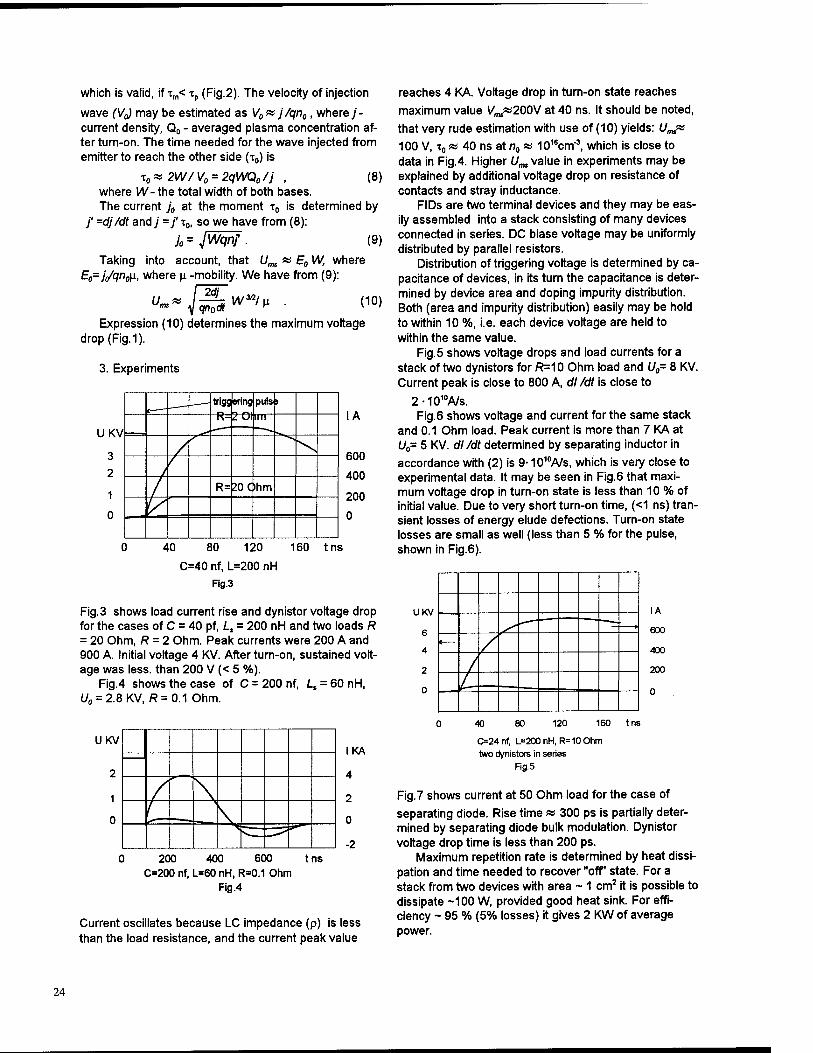
which is valid, if xm< tp (Fig.2). The velocity of injection
wave (Va) may be estimated as V0&j/qn0, where j- current density, Q0 - averaged plasma concentration af- ter turn-on. The time needed for the wave injected from emitter to reach the other side (T0) is
x0*2W/V0 = 2qWQ0/j , (8) where W-
.0*2W/V0 = 2qWQ0/j , the total width of both bases.
/ The current j0 at the moment T0 is determined by dj/dt andy =/T0. SO we nave from (8):
Jo=JWqnf- (9) Taking into account, that Um » E0 W, where
E0=j,/qn0\i, where u. -mobility. We have from (9):
"-«/ 2dj
qn^dt WM/u (10)
Expression (10) determines the maximum voltage drop(Fig.l).
3. Experiments
UKV
3 2
1
0
trigg sring puls > R- 2 Ol IITI
/
/ R= 20 C )hm
1/
600
400
200
0
0 40 80 120 160 tns
C=40 nf, L=200 nH Fig.3
Fig.3 shows load current rise and dynistor voltage drop for the cases of C = 40 pf, Ls = 200 nH and two loads R = 20 Ohm, R = 2 Ohm. Peak currents were 200 A and 900 A. Initial voltage 4 KV. After turn-on, sustained volt- age was less, than 200 V (< 5 %).
Fig.4 shows the case of C = 200 nf, L, = 60 nH, 170 = 2.8 KV.fi = 0.1 Ohm.
IKA UKV
2
1 /
*-—■
0 1
0 200 400 600 tns C=200 nf, L=60 nH, R=0.1 Ohm
Fig.4
Current oscillates because LC impedance (p) is less than the load resistance, and the current peak value
reaches 4 KA. Voltage drop in turn-on state reaches
maximum value v'TO»200V at 40 ns. It should be noted,
that very rude estimation with use of (10) yields: U^
100 V, t0» 40 ns at n0 « 1016cm"3, which is close to data in Fig.4. Higher Um value in experiments may be explained by additional voltage drop on resistance of contacts and stray inductance.
FIDs are two terminal devices and they may be eas- ily assembled into a stack consisting of many devices connected in series. DC biase voltage may be uniformly distributed by parallel resistors.
Distribution of triggering voltage is determined by ca- pacitance of devices, in its turn the capacitance is deter- mined by device area and doping impurity distribution. Both (area and impurity distribution) easily may be hold to within 10 %, i.e. each device voltage are held to within the same value.
Fig. 5 shows voltage drops and load currents for a stack of two dynistors for R=10 Ohm load and U0= 8 KV. Current peak is close to 800 A, dl/dt is close to
2-101°A/s. Fig.6 shows voltage and current for the same stack
and 0.1 Ohm load. Peak current is more than 7 KA at U0= 5 KV. dl/dt determined by separating inductor in
accordance with (2) is 9- 1010A/s, which is very close to experimental data. It may be seen in Fig.6 that maxi- mum voltage drop in turn-on state is less than 10 % of initial value. Due to very short turn-on time, (<1 ns) tran- sient losses of energy elude defections. Turn-on state losses are small as well (less than 5 % for the pulse, shown in Fig.6).
IA
600
400
200
o
0 40 80 120 160 tns
C=24nf, L=200nH,R=10Ohm two dynistors in series
Fig.5
Fig.7 shows current at 50 Ohm load for the case of
separating diode. Rise time » 300 ps is partially deter- mined by separating diode bulk modulation. Dynistor voltage drop time is less than 200 ps.
Maximum repetition rate is determined by heat dissi- pation and time needed to recover "off' state. For a stack from two devices with area ~ 1 cm2 it is possible to dissipate ~100 W, provided good heat sink. For effi- ciency - 95 % (5% losses) it gives 2 KW of average power.
UKV
6
4 t—
2
0
24
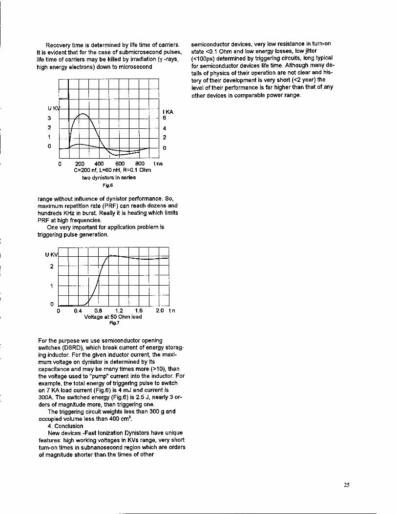
Recovery time is determined by life time of carriers. It is evident that for the case of submicrosecond pulses, life time of carriers may be killed by irradiation (y -rays, high energy electrons) down to microsecond
UK\
3
2
1
0
r
/ -N
/ \
/ \ —-» \
IKA 6
4
2
0
0 200 400 600 800 tns C=200 nf, L=60 nH, R=0.1 Ohm
two dynistors in series Fig.6
range without influence of dynistor performance. So, maximum repetition rate (PRF) can reach dozens and hundreds KHz in burst. Really it is heating which limits PRF at high frequencies.
One very important for application problem is triggering pulse generation.
semiconductor devices, very low resistance in turn-on state <0.1 Ohm and low energy losses, low jitter (<100ps) determined by triggering circuits, long typical for semiconductor devices life time. Although many de- tails of physics of their operation are not clear and his- tory of their development is very short (<2 year) the level of their performance is far higher than that of any other devices in comparable power range.
UKV
2
1
0 0.4 0.8 1.2 1.6
Voltage at 50 Ohm load Fig.7
2.0 tn
For the purpose we use semiconductor opening switches (DSRD), which break current of energy storag- ing inductor. For the given inductor current, the maxi- mum voltage on dynistor is determined by its capacitance and may be many times more (>10), than the voltage used to "pump" current into the inductor. For example, the total energy of triggering pulse to switch on 7 KA load current (Fig.6) is 4 mJ and current is 300A. The switched energy (Fig.6) is 2.5 J, nearly 3 or- ders of magnitude more, than triggering one.
The triggering circuit weights less than 300 g and occupied volume less than 400 cm3.
4. Conclusion New devices -Fast lonization Dynistors have unique
features: high working voltages in KVs range, very short turn-on times in subnanosecond region which are orders of magnitude shorter than the times of other
25
COMMUTATION OF STACKED BLUMLEIN PULSERS BY AVALANCHE GaAs SWITCHES
D.L. Borovina, J.L. Korioth, R.K. Krause, F. Davanloo and C.B. Collins
Canter for Quantum Electronics University of Texas at Dallas
P.O. Box 830688, Richardson, TX 75083-0688
F.J. Agee and J.H. Hull
Phillips Laboratory, PLIWSQ Kirtland AFB, NM 87117-6008
L.E. Kingsley
US. Army CECOM, S&TCD Ft. Monmouth, NJ 07703-5203
Abstract
Stacked Blumlein pulsers have produced high power waveforms with fast risetimes and a wide range of pulse durations and peak values using conventional thyratrons or spark gaps. This paper details our recent efforts to operate these pulsers with GaAs photoconductive switches in the avalanche mode. Adaptation of the design and fast charging schemes have enabled the stacked Blumleins to produce high-power nanosecond pulses with risetimes on the order of 200 - 300 ps. Significant progress is reported toward realiz- ing an intense, pulse power source for Ultra-WideBand HPM devices operating at 100 MW levels of power and kiloHertz repetition rates.
Introduction
The University of Texas at Dallas (UTD) first intro- duced and implemented a new approach for combining the functions of pulse shaping and voltage multiplication using stacked Blumleins. This resulted in the development of pulsers which consisted of several triaxial Blumleins stacked
in series at one end.1^ The lines were charged in parallel and synchronously commuted with a single switch at the other end. This allowed switching to take place at a low charging voltage relative to the pulser output voltage. These pulsers have been extensively characterized by our group and
their versatility has been demonstrated. 1_° Stacked Blum- lein pulsers have produced high-power waveforms with risetimes and repetition rates in the range of 5 - 50 ns and 1 - 200 Hz, respectively, using a conventional thyratron or spark gap. To generate waveforms with sub-nanosecond risetimes at kiloHertz repetition rates, fast switching devices, such as photoconductive switches, offer significant advan- tages.
In avalanche type photoconductive switches, the electron- hole pair produced by one photon is multiplied through an avalanche process, thus, reducing the optical energy required
for the initiation of switch closure. The reliability and performance of such avalanche type semiconductor switches depend on both the charging mechanisms and the operating environment. To realize the capabilities of these switches in stacked Blumlein pulsers, an intermediate module, which might be described as a charging pulse compression (CPC) module, was developed. The design and construction of the CPC were similar to that of single Blumlein pulse genera-
tors developed at UTD.9 The CPC conditioned the output of the pulse charging power supply so that the lines and the photoconductive switch in the final module were subjected to high voltage for less than 100 ns. This supported the use of avalanche photoconductive switches by increasing their lifetime.
Recently, a low profile switching assembly has been developed for the operation of photoconductive switches with
the stacked Blumlein pulsers."' *" The base of the assembly contained two copper electrodes which provided mechanical contact with the GaAs switch. The pressure cover was made from plexiglas and contained a chamber, into which the electrodes fit. To minimize the constriction of current flow to the switch from the pulse forming lines, the connections between the electrodes and the Blumlein were made using thin copper foils. The foils protruded from the base several centimeters to allow ample surface area for contact with the Blumlein and were passed through the cast material before it cured. The foils were joined to the electrodes by soldering them securely before immersion in the cast material. A 2-line version of the stacked Blumleins was then connected
to this universal switch assembly.1" During operation, the CPC was resonantly charged with
a pulse power supply capable of operating in the range of 3 - 75 kV at repetition rates of 1 - 1000 Hz. The output from the CPC device was used to charge the stacked Blumlein pulser in about 80 ns, after which a trigger pulse from the master oscillator Q-switched an Nd:YAG laser, providing
trigger photons in a 40-ns pulse for the GaAs switch. 10
26 0-7803-3076-5/96/S5.00 © 1996 IEEE
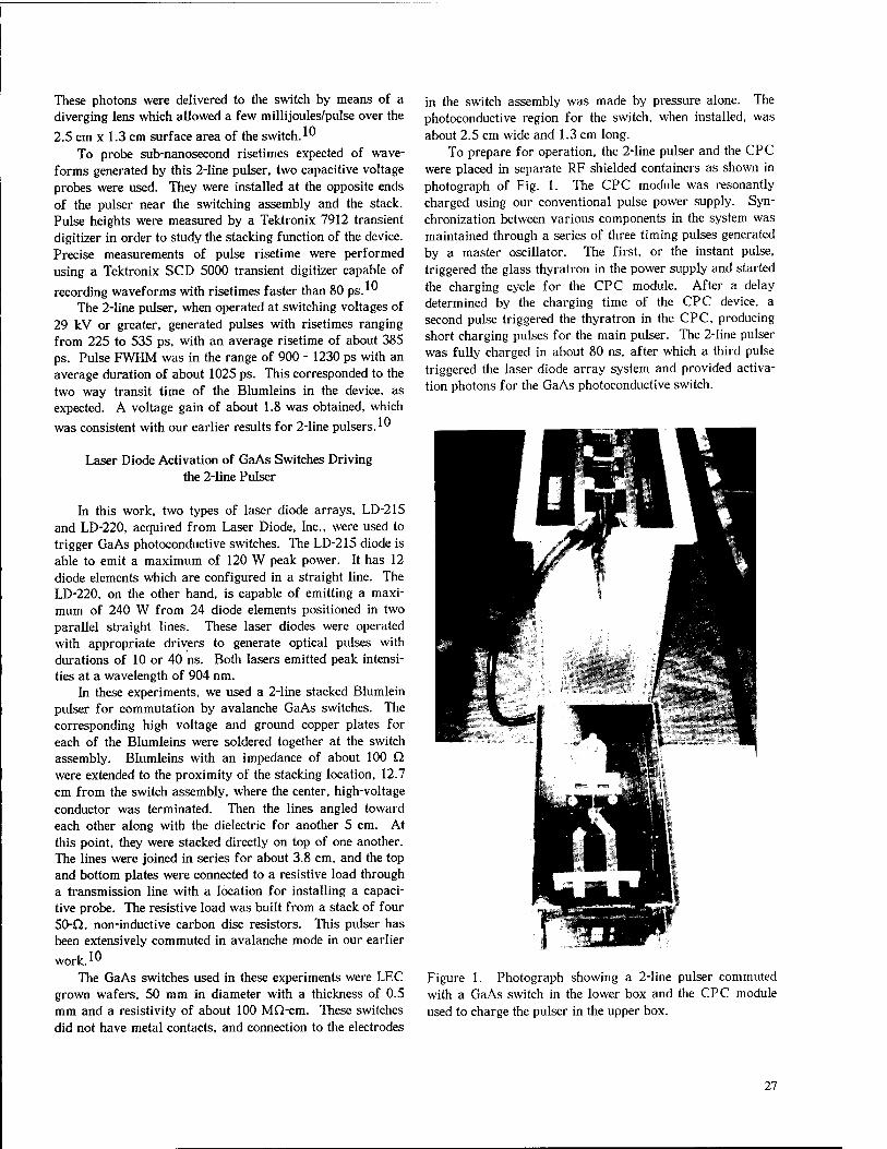
These photons were delivered to the switch by means of a diverging lens which allowed a few millijoules/pulse over the
2.5 cm x 1.3 cm surface area of the switch. 10
To probe sub-nanosecond risetimes expected of wave- forms generated by this 2-line pulser, two capacitive voltage probes were used. They were installed at the opposite ends of the pulser near the switching assembly and the stack. Pulse heights were measured by a Tektronix 7912 transient digitizer in order to study the stacking function of the device. Precise measurements of pulse risetime were performed using a Tektronix SCD 5000 transient digitizer capable of
recording waveforms with risetimes faster than 80 ps. The 2-line pulser, when operated at switching voltages of
29 kV or greater, generated pulses with risetimes ranging from 225 to 535 ps, with an average risetime of about 385 ps. Pulse FWHM was in the range of 900 - 1230 ps with an average duration of about 1025 ps. This corresponded to the two way transit time of the Blumleins in the device, as expected. A voltage gain of about 1.8 was obtained, which
was consistent with our earlier results for 2-line pulsers.10
Laser Diode Activation of GaAs Switches Driving the 2-line Pulser
In this work, two types of laser diode arrays, LD-215 and LD-220, acquired from Laser Diode, Inc., were used to trigger GaAs photoconductive switches. The LD-215 diode is able to emit a maximum of 120 W peak power. It has 12 diode elements which are configured in a straight line. The LD-220, on the other hand, is capable of emitting a maxi- mum of 240 W from 24 diode elements positioned in two parallel straight lines. These laser diodes were operated with appropriate drivers to generate optical pulses with durations of 10 or 40 ns. Both lasers emitted peak intensi- ties at a wavelength of 904 nm.
In these experiments, we used a 2-line stacked Blumlein pulser for commutation by avalanche GaAs switches. The corresponding high voltage and ground copper plates for each of the Blumleins were soldered together at the switch assembly. Blumleins with an impedance of about 100 Q were extended to the proximity of the stacking location, 12.7 cm from the switch assembly, where the center, high-voltage conductor was terminated. Then the lines angled toward each other along with the dielectric for another 5 cm. At this point, they were stacked directly on top of one another. The lines were joined in series for about 3.8 cm, and the top and bottom plates were connected to a resistive load through a transmission line with a location for installing a capaci- tive probe. The resistive load was built from a stack of four 50-Q, non-inductive carbon disc resistors. This pulser has been extensively commuted in avalanche mode in our earlier
work.10
The GaAs switches used in these experiments were LEC grown wafers, 50 mm in diameter with a thickness of 0.5 mm and a resistivity of about 100 MQ-cm. These switches did not have metal contacts, and connection to the electrodes
in the switch assembly was made by pressure alone. The photoconductive region for the switch, when installed, was about 2.5 cm wide and 1.3 cm long.
To prepare for operation, the 2-line pulser and the CPC were placed in separate RF shielded containers as shown in photograph of Fig. 1. The CPC module was resonantly charged using our conventional pulse power supply. Syn- chronization between various components in the system was maintained through a series of three timing pulses generated by a master oscillator. The first, or the instant pulse, triggered the glass thyratron in the power supply and started the charging cycle for the CPC module. After a delay determined by the charging time of the CPC device, a second pulse triggered the thyratron in the CPC, producing short charging pulses for the main pulser. The 2-line pulser was fully charged in about 80 ns, after which a third pulse triggered the laser diode array system and provided activa- tion photons for the GaAs photoconductive switch.
Figure 1. Photograph showing a 2-line pulser commuted with a GaAs switch in the lower box and the CPC module used to charge the pulser in the upper box.
27
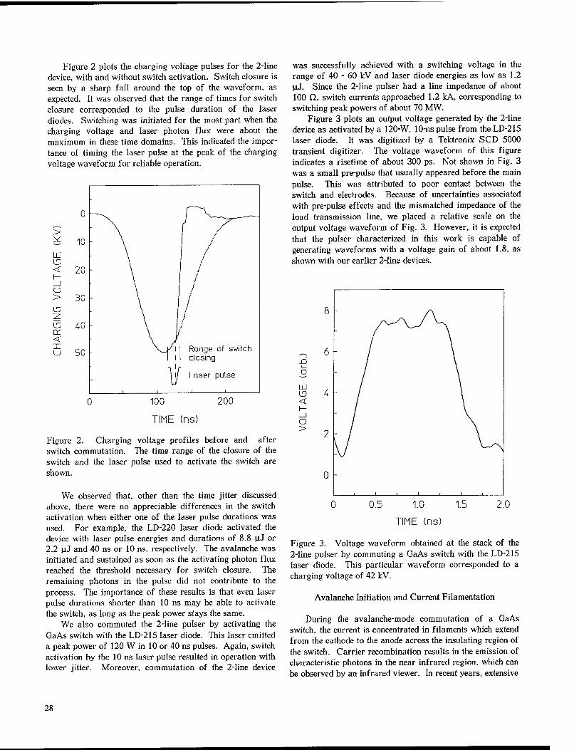
Figure 2 plots the charging voltage pulses for the 2-line device, with and without switch activation. Switch closure is seen by a sharp fall around the top of the waveform, as expected. It was observed that the range of times for switch closure corresponded to the pulse duration of the laser diodes. Switching was initiated for the most part when the charging voltage and laser photon flux were about the maximum in these time domains. This indicated the impor- tance of timing the laser pulse at the peak of the charging voltage waveform for reliable operation.
>
LLl ID < I— _J O > ID 2 ID cr < LJ
0
10 \ / \ /
20 \ f \ ■
\ i 30 \
40
50 N-J-'l I Range of switch I I I closing
11/ Laser pulse
i i i i...
100
TIME (ns)
200
Figure 2. Charging voltage profiles before and after switch commutation. The time range of the closure of the switch and the laser pulse used to activate the switch are shown.
We observed that, other than the time jitter discussed above, there were no appreciable differences in the switch activation when either one of the laser pulse durations was used. For example, the LD-220 laser diode activated the device with laser pulse energies and durations of 8.8 uJ or 2.2 uJ and 40 ns or 10 ns, respectively. The avalanche was initiated and sustained as soon as the activating photon flux reached the threshold necessary for switch closure. The remaining photons in the pulse did not contribute to the process. The importance of these results is that even laser pulse durations shorter than 10 ns may be able to activate the switch, as long as the peak power stays the same.
We also commuted the 2Tine pulser by activating the GaAs switch with the LD-215 laser diode. This laser emitted a peak power of 120 W in 10 or 40 ns pulses. Again, switch activation by the 10 ns laser pulse resulted in operation with lower jitter. Moreover, commutation of the 2-line device
was successfully achieved with a switching voltage in the range of 40 - 60 kV and laser diode energies as low as 1.2 pj. Since the 2-line pulser had a line impedance of about 100 Q, switch currents approached 1.2 kA, corresponding to switching peak powers of about 70 MW.
Figure 3 plots an output voltage generated by the 2-line device as activated by a 120-W, 10-ns pulse from the LD-215 laser diode. It was digitized by a Tektronix SCD 5000 transient digitizer. The voltage waveform of this figure indicates a risetime of about 300 ps. Not shown in Fig. 3 was a small pre-pulse that usually appeared before the main pulse. This was attributed to poor contact between the switch and electrodes. Because of uncertainties associated with pre-pulse effects and the mismatched impedance of the load transmission line, we placed a relative scale on the output voltage waveform of Fig. 3. However, it is expected that the pulser characterized in this work is capable of generating waveforms with a voltage gain of about 1.8, as shown with our earlier 2-line devices.
X) i_ a
UJ ID <
o >
0.5 1.0 1.5
TIME (ns)
Figure 3. Voltage waveform obtained at the stack of the 2Tine pulser by commuting a GaAs switch with the LD-215 laser diode. This particular waveform corresponded to a charging voltage of 42 kV.
Avalanche Initiation and Current Filamentation
During the avalanche-mode commutation of a GaAs switch, the current is concentrated in filaments which extend from the cathode to the anode across the insulating region of the switch. Carrier recombination results in the emission of characteristic photons in the near infrared region, which can be observed by an infrared viewer. In recent years, extensive
28
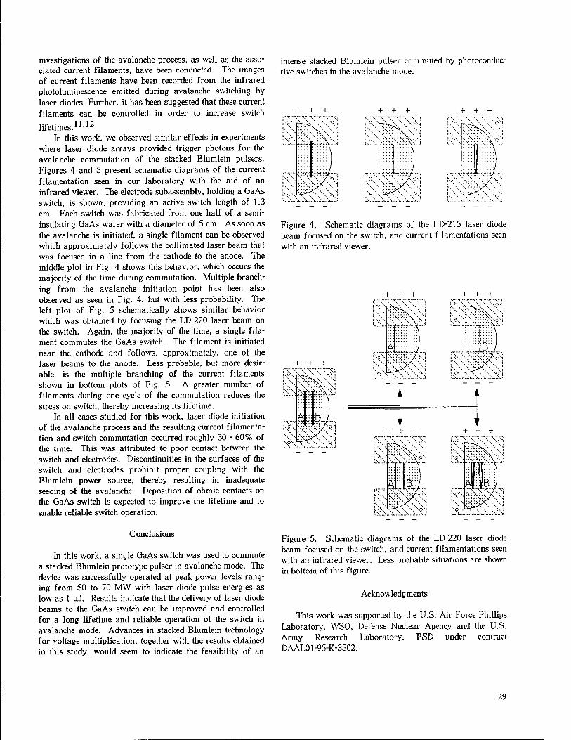
investigations of the avalanche process, as well as the asso- ciated current filaments, have been conducted. The images of current filaments have been recorded from the infrared photoluminescence emitted during avalanche switching by laser diodes. Further, it has been suggested that these current filaments can be controlled in order to increase switch
lifetimes.11-*2
In this work, we observed similar effects in experiments where laser diode arrays provided trigger photons for the avalanche commutation of the stacked Blumlein pulsers. Figures 4 and 5 present schematic diagrams of the current filamentation seen in our laboratory with the aid of an infrared viewer. The electrode subassembly, holding a GaAs switch, is shown, providing an active switch length of 1.3 cm. Each switch was fabricated from one half of a semi- insulating GaAs wafer with a diameter of 5 cm. As soon as the avalanche is initiated, a single filament can be observed which approximately follows the collimated laser beam that was focused in a line from the cathode to the anode. The middle plot in Fig. 4 shows this behavior, which occurs the majority of the time during commutation. Multiple branch- ing from the avalanche initiation point has been also observed as seen in Fig. 4, but with less probability. The left plot of Fig. 5 schematically shows similar behavior which was obtained by focusing the LD-220 laser beam on the switch. Again, the majority of the time, a single fila- ment commutes the GaAs switch. The filament is initiated near the cathode and follows, approximately, one of the laser beams to the anode. Less probable, but more desir- able, is the multiple branching of the current filaments shown in bottom plots of Fig. 5. A greater number of filaments during one cycle of the commutation reduces the stress on switch, thereby increasing its lifetime.
In all cases studied for this work, laser diode initiation of the avalanche process and the resulting current filamenta- tion and switch commutation occurred roughly 30 - 60% of the time. This was attributed to poor contact between the switch and electrodes. Discontinuities in the surfaces of the switch and electrodes prohibit proper coupling with the Blumlein power source, thereby resulting in inadequate seeding of the avalanche. Deposition of ohmic contacts on the GaAs switch is expected to improve the lifetime and to enable reliable switch operation.
intense stacked Blumlein pulser commuted by photoconduc- tive switches in the avalanche mode.
+ + + + +
Figure 4. Schematic diagrams of the LD-215 laser diode beam focused on the switch, and current filamentations seen with an infrared viewer.
+ + +
+ + +
+ + + + + +
>*J:C ;-.':;VI
4- ̂,''*?n/*'
Conclusions
In this work, a single GaAs switch was used to commute a stacked Blumlein prototype pulser in avalanche mode. The device was successfully operated at peak power levels rang- ing from 50 to 70 MW with laser diode pulse energies as low as 1 \sJ. Results indicate that the delivery of laser diode beams to the GaAs switch can be improved and controlled for a long lifetime and reliable operation of the switch in avalanche mode. Advances in stacked Blumlein technology for voltage multiplication, together with the results obtained in this study, would seem to indicate the feasibility of an
Figure 5. Schematic diagrams of the LD-220 laser diode beam focused on the switch, and current filamentations seen with an infrared viewer. Less probable situations are shown in bottom of this figure.
Acknowledgments
This work was supported by the U.S. Air Force Phillips Laboratory, WSQ, Defense Nuclear Agency and the U.S. Army Research Laboratory, PSD under contract DAAL01-95-K-3502.
29
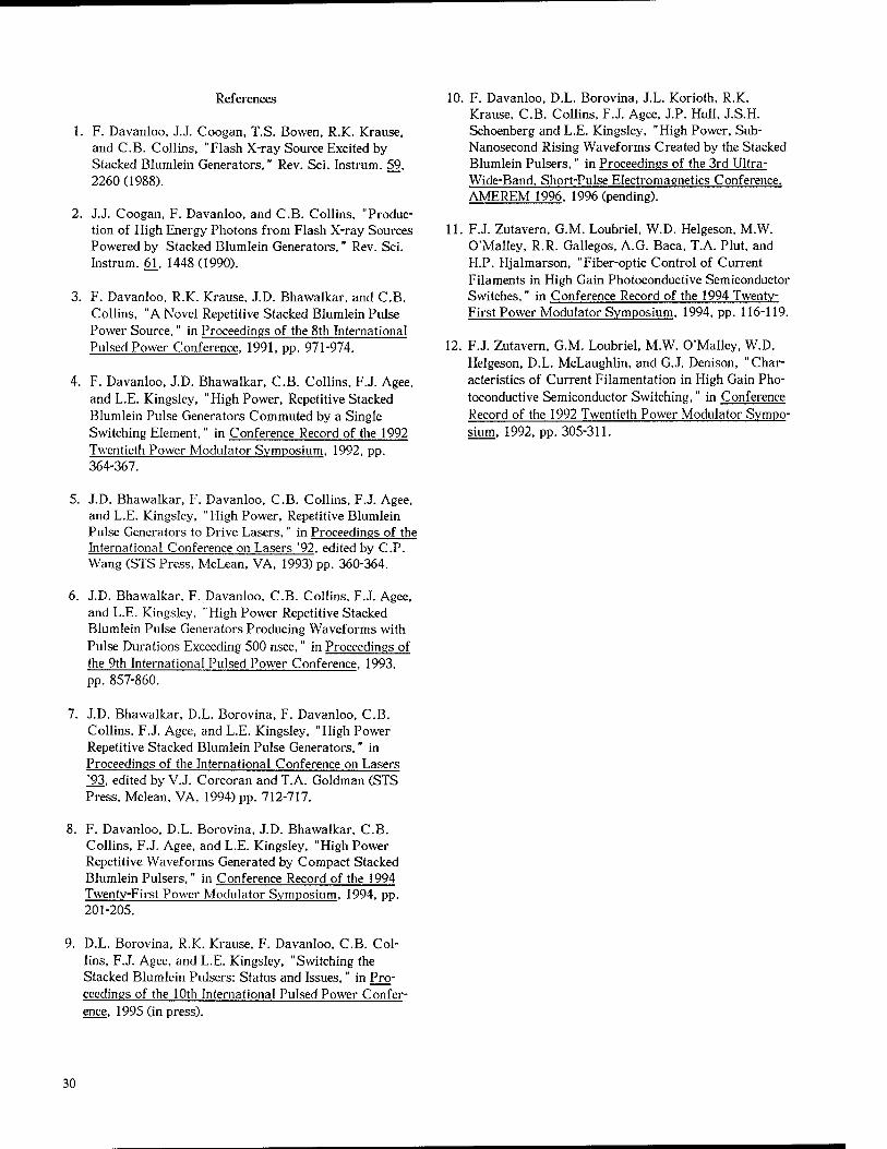
References
1. F. Davanloo, J.J. Coogan, T.S. Bowen, R.K. Krause, and C.B. Collins, "Flash X-ray Source Excited by Stacked Blumlein Generators," Rev. Sei. Instrum. 59, 2260 (1988).
2. J.J. Coogan, F. Davanloo, and C.B. Collins, "Produc- tion of High Energy Photons from Flash X-ray Sources Powered by Stacked Blumlein Generators," Rev. Sei. Instrum. 61, 1448 (1990).
3. F. Davanloo, R.K. Krause, J.D. Bhawalkar, and C.B. Collins, "A Novel Repetitive Stacked Blumlein Pulse Power Source," in Proceedings of the 8th International Pulsed Power Conference, 1991, pp. 971-974.
4. F. Davanloo, J.D. Bhawalkar, C.B. Collins, F.J. Agee, and L.E. Kingsley, "High Power, Repetitive Stacked Blumlein Pulse Generators Commuted by a Single Switching Element," in Conference Record of the 1992 Twentieth Power Modulator Symposium, 1992, pp. 364-367.
5. J.D. Bhawalkar, F. Davanloo, C.B. Collins, F.J. Agee, and L.E. Kingsley, "High Power, Repetitive Blumlein Pulse Generators to Drive Lasers," in Proceedings of the International Conference on Lasers '92, edited by C.P. Wang (STS Press, McLean, VA, 1993) pp. 360-364.
10. F. Davanloo, D.L. Borovina, J.L. Korioth, R.K. Krause, C.B. Collins, F.J. Agee, J.P. Hull, J.S.H. Schoenberg and L.E. Kingsley, "High Power, Sub- Nanosecond Rising Waveforms Created by the Stacked Blumlein Pulsers," in Proceedings of the 3rd Ultra- Wide-Band, Short-Pulse Electromagnetics Conference, AMEREM 1996, 1996 (pending).
11. F.J. Zutavern, G.M. Loubriel, W.D. Helgeson, M.W. O'Malley, R.R. Gallegos, A.G. Baca, T.A. Plut, and H.P. Hjalmarson, "Fiber-optic Control of Current Filaments in High Gain Photoconductive Semiconductor Switches," in Conference Record of the 1994 Twenty- First Power Modulator Symposium, 1994, pp. 116-119.
12. F.J. Zutavern, G.M. Loubriel, M.W. O'Malley, W.D. Helgeson, D.L. McLaughlin, and G.J. Denison, " Char- acteristics of Current Filamentation in High Gain Pho- toconductive Semiconductor Switching," in Conference Record of the 1992 Twentieth Power Modulator Sympo- sium, 1992, pp. 305-311.
6. J.D. Bhawalkar, F. Davanloo, C.B. Collins, F.J. Agee, and L.E. Kingsley, "High Power Repetitive Stacked Blumlein Pulse Generators Producing Waveforms with Pulse Durations Exceeding 500 nsec," in Proceedings of the 9th International Pulsed Power Conference, pp. 857-860.
1993,
7. J.D. Bhawalkar, D.L. Borovina, F. Davanloo, C.B. Collins, F.J. Agee, and L.E. Kingsley, "High Power Repetitive Stacked Blumlein Pulse Generators," in Proceedings of the International Conference on Lasers '93, edited by V.J. Corcoran and T.A. Goldman (STS Press, Mclean, VA, 1994) pp. 712-717.
8. F. Davanloo, D.L. Borovina, J.D. Bhawalkar, C.B. Collins, F.J. Agee, and L.E. Kingsley, "High Power Repetitive Waveforms Generated by Compact Stacked Blumlein Pulsers," in Conference Record of the 1994 Twenty-First Power Modulator Symposium, 1994, pp. 201-205.
9. D.L. Borovina, R.K. Krause, F. Davanloo, C.B. Col- lins, F.J. Agee, and L.E. Kingsley, "Switching the Stacked Blumlein Pulsers: Status and Issues," in Pro- ceedings of the 10th International Pulsed Power Confer- ence, 1995 (in press).
30
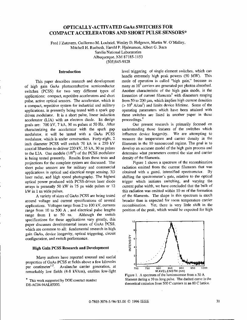
OPTICALLY-ACTIVATED GaAs SWITCHES FOR COMPACT ACCELERATORS AND SHORT PULSE SENSORS*
Fred J Zutavern, Guillermo M. Loubriel, Wesley D. Helgeson, Martin W. O'Malley, Mitchell H. Ruebush, Harold P. Hjalmarson, Albert G. Baca
Sandia National Laboratories Albuquerque, NM 87185-1153
(505)845-9128
Introduction
This paper describes research and development of high gain GaAs photoconductive semiconductor switches (PCSS) for two very different types of applications: compact, repetitive accelerators and short pulse, active optical sensors. The accelerator, which is a compact, repetitive system for industrial and military applications, is presently being tested with a spark gap driven modulator. It is a short pulse, linear induction accelerator (LIA) with an electron diode. Its design goals are: 700 kV, 7 kA, 30 ns pulses at 50 Hz. After characterizing the accelerator with the spark gap modulator, it will be tested with a GaAs PCSS modulator, which is under construction. Forty-eight, 2 inch diameter PCSS will switch 70 kA in a 250 kV coaxial Blumlein to deliver 220 kV, 35 kA, 30 ns pulses to the LIA. One module (1/8*) of the PCSS modulator is being tested presently. Results from these tests and projections for the complete system are discussed. The short pulse sensors are for military and commercial applications in optical and electrical range sensing, 3D laser radar, and high speed photography. The highest optical power produced with PCSS-driven laser diode arrays is presently 50 kW in 75 ps wide pulses or 12 kW in 1 ns wide pulses.
A variety of sizes of GaAs PCSS are being tested around voltage and current specifications of several applications. Voltages range from 2 to 100 kV, currents range from 10 to 500 A , and electrical pulse lengths range from 1 to 50 ns. Although the switch specifications for these applications vary greatly, this paper discusses developmental issues of GaAs PCSS, which are common to all: fundamental research in high gain GaAs, device longevity, optical triggering, circuit configuration, and switch performance.
High Gain PCSS Research and Development
Many authors have reported unusual and useful properties of GaAs PCSS at fields above a few kilovolts per centimeter1,2. Avalanche carrier generation, at remarkably low fields (4-8 kV/cm), enables low-light
level triggering of single element switches, which can handle extremely high peak powers (50 MW). This mode of operation is called "high gain," because as many as 105 carriers are generated per photon absorbed. Another characteristic of the high gain mode, is the formation of current filaments3 with diameters ranging from 50 to 200 urn, which implies high current densities (> 106 A/cm2) and limits device lifetime. Some of the operating parameters which have been attained with these switches are listed in another paper in these proceedings.4
Our present research is primarily focused on understanding those features of the switches which influence device longevity. We are attempting to measure the temperature and carrier density in the filaments in the 10 nanosecond regime. The goal is to develop an accurate model of the high gain process and determine what parameters control the size and carrier density of the filaments.
Figure 1 shows a spectrum of the recombination radiation emitted from the current filaments that was obtained with a gated, intensified spectrometer. By shifting the spectrometer's gate, relative to the optical trigger which initiates switching, and varying the current pulse width, we have concluded that the bulk of this radiation was emitted within 10 ns of the formation of the filaments. The shape in this spectrum is much broader than is expected for room temperature carrier recombination. Yet, there is very little shift in the position of the peak, which would be expected for high
10
8
-—— 1 1 rj 1 1
> t 6 CO z LXJ 1- 4 Z 7 \ 2
0
This work supported by DOE contract number DE-AC04-94AL85000.
700 750 800 850 900 950 1000 WAVELENGTH (nm)
Figure 1. A spectrum of the luminescence from a 30 A filament during a 10 ns long pulse. The dashed curve is the theoretical emission from 500 C carriers in an 80 C lattice.
0-7803-3076-5/96/S5.00 © 1996 IEEE 31
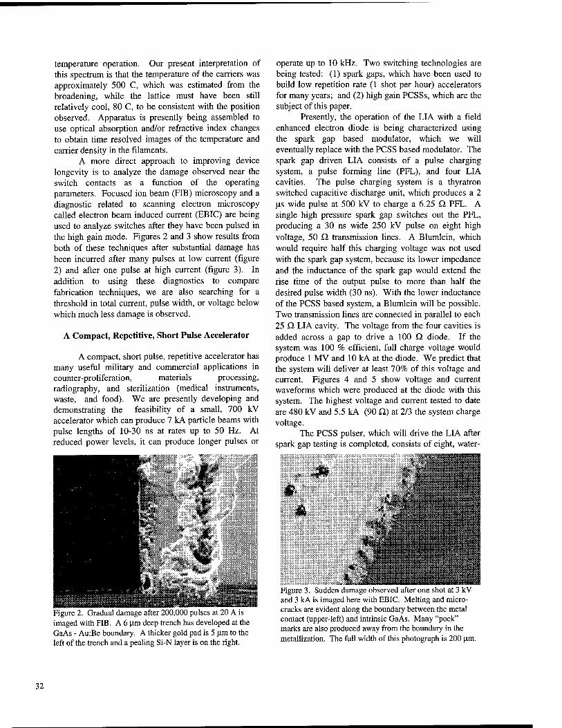
temperature operation. Our present interpretation of this spectrum is that the temperature of the carriers was approximately 500 C, which was estimated from the broadening, while the lattice must have been still relatively cool, 80 C, to be consistent with the position observed. Apparatus is presently being assembled to use optical absorption and/or refractive index changes to obtain time resolved images of the temperature and carrier density in the filaments.
A more direct approach to improving device longevity is to analyze the damage observed near the switch contacts as a function of the operating parameters. Focused ion beam (FIB) microscopy and a diagnostic related to scanning electron microscopy called electron beam induced current (EBIC) are being used to analyze switches after they have been pulsed in the high gain mode. Figures 2 and 3 show results from both of these techniques after substantial damage has been incurred after many pulses at low current (figure 2) and after one pulse at high current (figure 3). In addition to using these diagnostics to compare fabrication techniques, we are also searching for a threshold in total current, pulse width, or voltage below which much less damage is observed.
A Compact, Repetitive, Short Pulse Accelerator
A compact, short pulse, repetitive accelerator has many useful military and commercial applications in counter-proliferation, materials processing, radiography, and sterilization (medical instruments, waste, and food). We are presently developing and demonstrating the feasibility of a small, 700 kV accelerator which can produce 7 kA particle beams with pulse lengths of 10-30 ns at rates up to 50 Hz. At reduced power levels, it can produce longer pulses or
:S'-.",7,SH.
operate up to 10 kHz. Two switching technologies are being tested: (1) spark gaps, which have been used to build low repetition rate (1 shot per hour) accelerators for many years; and (2) high gain PCSSs, which are the subject of this paper.
Presently, the operation of the LIA with a field enhanced electron diode is being characterized using the spark gap based modulator, which we will eventually replace with the PCSS based modulator. The spark gap driven LIA consists of a pulse charging system, a pulse forming line (PFL), and four LIA cavities. The pulse charging system is a thyratron switched capacitive discharge unit, which produces a 2 us wide pulse at 500 kV to charge a 6.25 Q. PFL. A single high pressure spark gap switches out the PFL, producing a 30 ns wide 250 kV pulse on eight high voltage, 50 Q. transmission lines. A Blumlein, which would require half this charging voltage was not used with the spark gap system, because its lower impedance and the inductance of the spark gap would extend the rise time of the output pulse to more than half the desired pulse width (30 ns). With the lower inductance of the PCSS based system, a Blumlein will be possible. Two transmission lines are connected in parallel to each 25 D. LIA cavity. The voltage from the four cavities is added across a gap to drive a 100 £1 diode. If the system was 100 % efficient, full charge voltage would produce 1 MV and 10 kA at the diode. We predict that the system will deliver at least 70% of this voltage and current. Figures 4 and 5 show voltage and current waveforms which were produced at the diode with this system. The highest voltage and current tested to date are 480 kV and 5.5 kA (90 Q.) at 2/3 the system charge voltage.
The PCSS pulser, which will drive the LIA after spark gap testing is completed, consists of eight, water-
'"iiP'G
*
•v v>^ ■ ■'■/■■'.
■. v;i|::|;::|:'
/ «'-jtfc.-V...- ,4;=; 1 \ T'T" ■*■"'■:..''■ Xty-■rP.Wri
:■• . 51* =
¥.'■■■%.-
mi $■■£■ V^^V^V-^ |j|§§§§
...;'•■ ^".! ll||l§
51 ■^iJW? u
■•» " :-f-^r\ ••*•» • ,. .;; >:;-S---'-;.M."-- -:Ü
Figure 2. Gradual damage after 200,000 pulses at 20 A is imaged with FIB. A 6 urn deep trench has developed at the GaAs - Au:Be boundary. A thicker gold pad is 5 urn to the left of the trench and a pealing Si-N layer is on the right.
Figure 3. Sudden damage observed after one shot at 3 kV and 3 kA is imaged here with EBIC. Melting and micro- cracKS are evident aiong uie uounaary ueiween me meiai contact (upper-left) and intrinsic GaAs. Many "pock" marks are also produced away from the boundary in the metallization. The full width of this photograph is 200 urn.
32
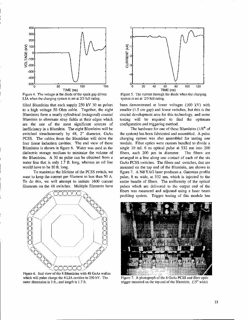
400
50 100 150 TIME (ns)
Figure 4. The voltage at the diode of the spark gap driven LIA when the charging system is set at 2/3 full rating.
filled Blumleins that each supply 250 kV 30 ns pulses to a high voltage 50 Ohm cable. Together, the eight Blumleins form a nearly cylindrical (octagonal) coaxial Blumlein to eliminate stray fields at their edges which are the one of the most significant sources of inefficiency in a Blumlein. The eight Blumleins will be switched simultaneously by 48, 2" diameter, GaAs PCSS. The cables from the Blumleins will drive the four linear induction cavities. The end view of these Blumleins is shown in figure 6. Water was used as the dielectric storage medium to minimize the volume of the Blumleins. A 30 ns pulse can be obtained from a water line that is only 1.7 ft. long, whereas an oil line would have to be 10 ft. long.
To maximize the lifetime of the PCSS switch, we want to keep the current per filament to less than 50 A. To do this, we will attempt to initiate 1600 current filaments on the 48 switches. Multiple filaments have
60 80 TIME (ns)
Figure 5. The current through the diode when the charging system is set at 2/3 full rating.
been demonstrated at lower voltages (100 kV) with smaller (1.5 cm gap) and fewer switches, but this is the crucial development area for this technology, and some testing will be required to find the optimum configuration and triggering method.
The hardware for one of these Blumleins (1/8* of the system) has been fabricated and assembled. A pulse charging system was also assembled for testing one module. Fiber optics were custom bundled to divide a single 10 mJ, 6 ns optical pulse at 532 nm into 200 fibers, each 200 u.m in diameter. The fibers are arranged in a line along one contact of each of the six GaAs PCSS switches. The fibers and switches, that are mounted on the top end of the Blumlein, are shown in figure 7. A Nd:YAG laser produces a Gaussian profile pulse, 8 ns wide, at 532 nm, which is injected to the entire bundle of fibers. The uniformity of the optical pulses which are delivered to the output end of the fibers was measured and adjusted using a laser beam profiling system. Trigger testing of this module has
Figure 6. End view of the 8 Blumleins with 48 GaAs wafers which will pulse charge the 4 LIA cavities to 250 kV. The outer dimension is 3 ft., and length is 1.7 ft.
Figure 7. A photograph of the 6 GaAs PCSS and fiber optic trigger mounted on the top end of the Blumlein. (15" wide)
33
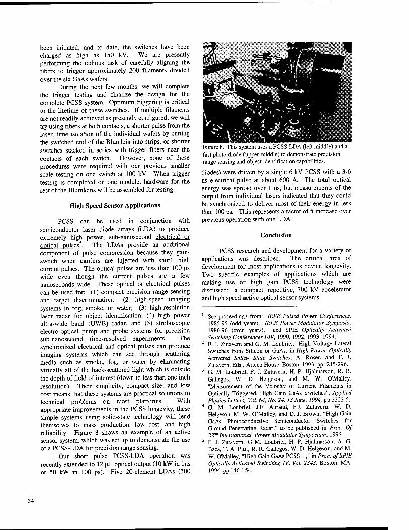
been initiated, and to date, the switches have been charged as high as 150 kV. We are presently performing the tedious task of carefully aligning the fibers to trigger approximately 200 filaments divided over the six GaAs wafers.
During the next few months, we will complete the trigger testing and finalize the design for the complete PCSS system. Optimum triggering is critical to the lifetime of these switches. If multiple filaments are not readily achieved as presently configured, we will try using fibers at both contacts, a shorter pulse from the laser, time isolation of the individual wafers by cutting the switched end of the Blumlein into strips, or shorter switches stacked in series with trigger fibers near the contacts of each switch. However, none of these procedures were required with our previous smaller scale testing on one switch at 100 kV. When trigger testing is completed on one module, hardware for the rest of the Blumleins will be assembled for testing.
High Speed Sensor Applications
PCSS can be used in conjunction with semiconductor laser diode arrays (LDA) to produce extremely high power, sub-nanosecond electrical or optical pulses5. The LDAs provide an additional component of pulse compression because they gain- switch when carriers are injected with short, high current pulses. The optical pulses are less than 100 ps wide even though the current pulses are a few nanoseconds wide. These optical or electrical pulses can be used for: (1) compact precision range sensing and target discrimination; (2) high-speed imaging systems in fog, smoke, or water; (3) high-resolution laser radar for object identification; (4) high power ultra-wide band (UWB) radar, and (5) stroboscopic electro-optical pump and probe systems for precision sub-nanosecond time-resolved experiments. The synchronized electrical and optical pulses can produce imaging systems which can see through scattering media such as smoke, fog, or water by eliminating virtually all of the back-scattered light which is outside the depth of field of interest (down to less than one inch resolution). Their simplicity, compact size, and low cost means that these systems are practical solutions to technical problems on most platforms. With appropriate improvements in the PCSS longevity, these simple systems using solid-state technology will lend themselves to mass production, low cost, and high reliability. Figure 8 shows an example of an active sensor system, which was set up to demonstrate the use of a PCSS-LDA for precision range sensing.
Our short pulse PCSS-LDA operation was recently extended to 12 uJ optical output (10 kW in Ins or 50 kW in 100 ps). Five 20-element LDAs (100
Figure 8. This system uses a PCSS-LDA (left middle) and a fast photo-diode (upper-middle) to demonstrate precision range sensing and object identification capabilities.
diodes) were driven by a single 6 kV PCSS with a 3-6 ns electrical pulse at about 600 A. The total optical energy was spread over 1 ns, but measurements of the output from individual lasers indicated that they could be synchronized to deliver most of their energy in less than 100 ps. This represents a factor of 5 increase over previous operation with one LDA.
Conclusion
PCSS research and development for a variety of applications was described. The critical area of development for most applications is device longevity. Two specific examples of applications which are making use of high gain PCSS technology were discussed: a compact, repetitive, 700 kV accelerator and high speed active optical sensor systems.
1 See proceedings from: IEEE Pulsed Power Conferences, 1985-95 (odd years), IEEE Power Modulator Symposia, 1986-96 (even years), and SPIE Optically Activated Switching Conferences I-IV, 1990, 1992, 1993, 1994.
2 F. J. Zutavern and G. M. Loubriel, "High Voltage Lateral Switches from Silicon or GaAs, in High-Power Optically Activated Solid- State Switches, A. Rosen and F. J. Zutavern, Eds., Artech House, Boston, 1993, pp. 245-296.
3 G. M. Loubriel, F. J. Zutavern, H. P. Hjalmarson, R. R. Gallegos, W. D. Helgeson, and M. W. O'Malley, "Measurement of the Velocity of Current Filaments in Optically Triggered, High Gain GaAs Switches", Applied Physics Utters, Vol. 64, No. 24, 13 June, 1994, pp 3323-5.
4 G. M. Loubriel, J.F. Aurand, F.J. Zutavern, W. D. Helgeson, M. W. O'Malley, and D. J. Brown, "High Gain GaAs Photoconductive Semiconductor Switches for Ground Penetrating Radar," to be published in Proc. Of 22nd International Power Modulator Symposium, 1996.
5 F. J. Zutavern, G M. Loubriel, H. P. Hjalmarson, A. G. Baca, T. A. Plut, R. R. Gallegos, W. D. Helgeson, and M. W. O'Malley, "High Gain GaAs PCSS...," in Proc. of SPIE Optically Activated Switching IV, Vol. 2343, Boston, MA, 1994, pp 146-154.
34
High Voltage GaAs Rectifiers for High Frequency, High Power Density
Switching Applications
P. Hadizad, J. Ommen, A. Salih, S. Varadarajan, R. Slocumb, E. Robles, and M. Wölk Motorola, Power Products Division 5005 E. McDowell Road, MD-Z311
Phoenix, Arizona 85008 (602) 244-6304
&
C. Thero Motorola, Phoenix Corporate Research Laboratories
2100 E. Elliot Road, MD-EL508 Tempe, Arizona 85008
(602) 413-5562
Introduction
High voltage (>500 V), fast recovery silicon p-i-n diodes are currently an integral component of 300-400V DC switched-mode power supplies operating in the frequency range of 80-100 kHz. At these frequencies, the device's switching losses lead to Joule heating, resulting in high average junction temperatures, long reverse recovery times (>100 ns), and device instability. As a result, while the power supply's operating frequency is limited to -100 kHz, complex and costly designs for circumventing the diode's reverse recovery losses and removal of the excess generated heat are to be implemented.
As compared to silicon, if designed for equal values of avalanche breakdown voltage and on-state current density, the larger energy bandgap of GaAs, along with its high electron mobility, result in majority carrier devices (Schottky diodes and field-effect transistors) with significantly (>5 times) lower values of on-resistance. Furthermore, in the case of conductivity modulated devices, based on the larger energy bandgap and the fast recombination lifetime of minority carriers, GaAs devices exhibit extremely low, nearly temperature independent values of reverse recovery stored charge (25 C < T < 175 C). This, along with the higher intrinsic temperature of GaAs, allow for the design of high power density (output power / volume) switched-mode power supplies operating at high switching frequencies (250 - 500 kHz).
The development and reliability studies of high voltage, high efficiency GaAs Merged p-n / Schottky (MPS) rectifiers are herein reported. These devices exhibit extremely low switching losses, along with DC breakdown voltage of
500-1000V, and average rectified forward current of 8-10 A, at on-state voltage of -2 volts. The rated DC avalanche breakdown voltage is >90% of the ideal (theoretical) value. Results on the optimization of the device performance using two dimensional device simulations (TMA MEDICI) and Design of Experiments (DOE) methodology are reviewed. Implementation of these devices in high frequency switching systems are also discussed.
Device Simulation
The GaAs MPS diode structure is shown in Fig. 1. In theory, the ideal avalanche breakdown voltage of a semiconductor junction is determined assuming an abrupt, parallel plate junction with an infinite radius of curvature.1 In our study, two dimensional device simulations were performed on parallel-plate Schottky/ n-type GaAs diodes using TMA MEDICI.2 Based on results obtained, the epitaxial layer dopant concentration and thickness were optimized to achieve ideal breakdown voltage of 500V to 1000V.
In actual power devices, the finite radius of curvature of the voltage blocking junction results in electric field crowding at the junction edge, leading to premature avalanche breakdown. During the course of this work, various junction edge termination structures were investigated, in order to optimize the electric field distribution and achieve nearly ideal values of simulated breakdown voltage.3
The floating ring structure is an edge termination structure which is widely used in the silicon technology for achieving near ideal values of breakdown voltage.4 In this case, the rings are formed via ion implantation and subsequent
0-7803-3076-5/96/55.00 © 1996 IEEE 35
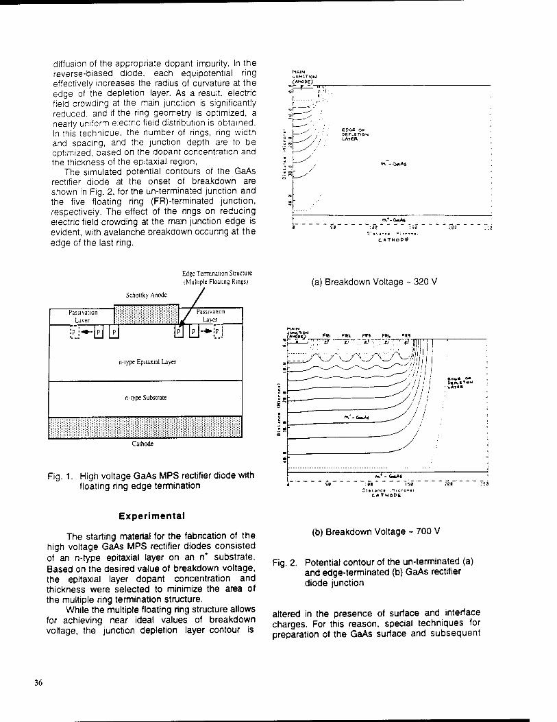
diffusion of the appropriate dopant impurity. In the reverse-biased diode, each equipotential ring effectively increases the radius of curvature at the edge of the depletion layer. As a result, electric field crowding at the main junction is significantly reduced, and if the ring geometry is optimized, a nearly uniform electric field distribution is obtained. In this technique, the number of rings, ring width and spacing, and the junction depth are to be optimized, based on the dopant concentration and the thickness of the epitaxial region,
The simulated potential contours of the GaAs rectifier diode at the onset of breakdown are shown in Fig. 2, for the un-terminated junction and the five floating ring (FR)-terminated junction, respectively. The effect of the rings on reducing electric field crowding at the main junction edge is evident, with avalanche breakdown occuring at the edge of the last ring.
MAIN JUNCTlflM
-f- r l!;l 1 '
' " ,' '
COGfi OP DEPLETION LA7£A
m -0*l<*5
r^/
m+-<~M 59 :ae :sa ;aa
CATHoDS
Edge Termination Structure (Multiple Floating Rings)
Schottky Anode
Passivation Laver
/ Passivation J Layer
£>-[pj [p] [i
n-type Epitaxial Layer
j lil"*ip.i
n-type Substrate
:
Fig
Cathode
1. High voltage GaAs MPS rectifier diode with floating ring edge termination
(a) Breakdown Voltage - 320 V
tXcitT FRi Fin m f*k F«5 la^'i; ;:'*> ;"-v" ■■■t}:,---tJ-yy^m\\i
I»» • <—>l
:lt l5B ]illinci 11c^O«t)
caTMODC
Experimental
The starting material for the fabrication of the high voltage GaAs MPS rectifier diodes consisted of an n-type epitaxial layer on an n+ substrate. Based on the desired value of breakdown voltage, the epitaxial layer dopant concentration and thickness were selected to minimize the area of the multiple ring termination structure.
While the multiple floating ring structure allows for achieving near ideal values of breakdown voltage, the junction depletion layer contour is
(b) Breakdown Voltage - 700 V
Fig. 2. Potential contour of the un-terminated (a) and edge-terminated (b) GaAs rectifier diode junction
altered in the presence of surface and interface charges. For this reason, special techniques for preparation of the GaAs surface and subsequent
36
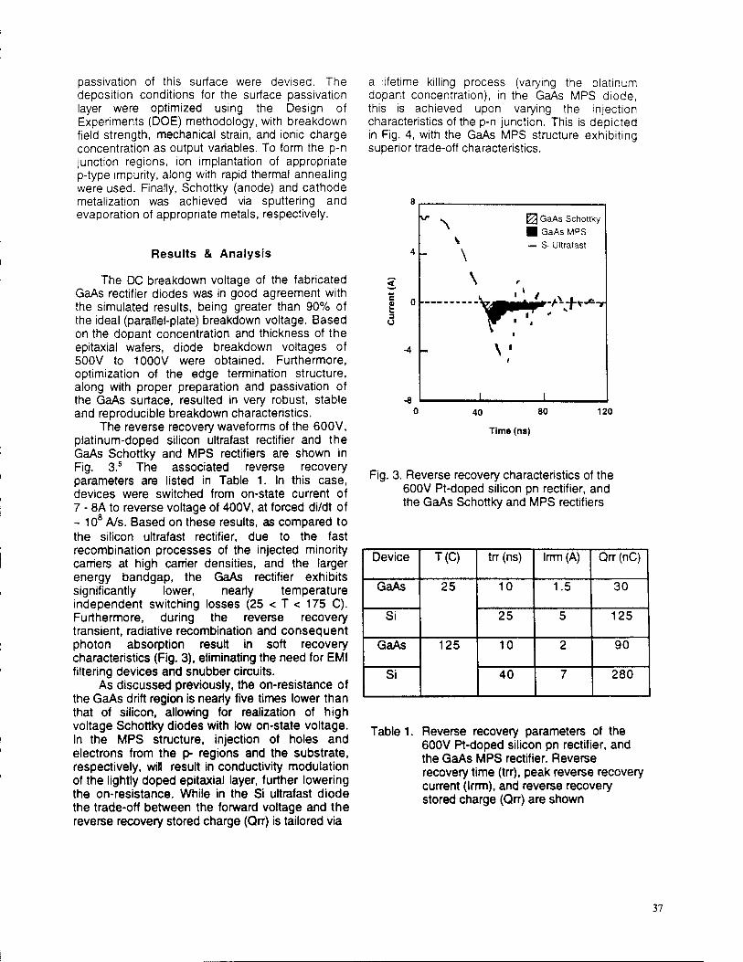
passivation of this surface were devised. The deposition conditions for the surface passivation layer were optimized using the Design of Experiments (DOE) methodology, with breakdown field strength, mechanical strain, and ionic charge concentration as output variables. To form the p-n junction regions, ion implantation of appropriate p-type impurity, along with rapid thermal annealing were used. Finally, Schottky (anode) and cathode metalization was achieved via sputtering and evaporation of appropriate metals, respectively.
Results & Analysis
The DC breakdown voltage of the fabricated GaAs rectifier diodes was in good agreement with the simulated results, being greater than 90% of the ideal (parallel-plate) breakdown voltage. Based on the dopant concentration and thickness of the epitaxial wafers, diode breakdown voltages of 500V to 1000V were obtained. Furthermore, optimization of the edge termination structure, along with proper preparation and passivation of the GaAs surface, resulted in very robust, stable and reproducible breakdown characteristics.
The reverse recovery waveforms of the 600V, platinum-doped silicon ultrafast rectifier and the GaAs Schottky and MPS rectifiers are shown in Fig. 3.5 The associated reverse recovery parameters are listed in Table 1. In this case, devices were switched from on-state current of 7 - 8A to reverse voltage of 400V, at forced di/dt of - 108 A/s. Based on these results, as compared to the silicon ultrafast rectifier, due to the fast recombination processes of the injected minority carriers at high carrier densities, and the larger energy bandgap, the GaAs rectifier exhibits significantly lower, nearly temperature independent switching losses (25 < T < 175 C). Furthermore, during the reverse recovery transient, radiative recombination and consequent photon absorption result in soft recovery characteristics (Fig. 3), eliminating the need for EMI filtering devices and snubber circuits.
As discussed previously, the on-resistance of the GaAs drift region is nearly five times lower than that of silicon, allowing for realization of high voltage Schottky diodes with low on-state voltage. In the MPS structure, injection of holes and electrons from the p- regions and the substrate, respectively, will result in conductivity modulation of the lightly doped epitaxial layer, further lowering the on-resistance. While in the Si ultrafast diode the trade-off between the forward voltage and the reverse recovery stored charge (Qrr) is tailored via
a lifetime killing process (varying the platinum dopant concentration), in the GaAs MPS diode, this is achieved upon varying the injection characteristics of the p-n junction. This is depicted in Fig. 4, with the GaAs MPS structure exhibiting superior trade-off characteristics.
4 _
3 o
\ 0 GaAs Schottky
■ GaAs MPS — Si Ultrafast
\ Ay. ■'''• A\+r^-r
_L 40 80
Time (ns)
120
Fig. 3. Reverse recovery characteristics of the 600V Pt-doped silicon pn rectifier, and the GaAs Schottky and MPS rectifiers
Device T(C) trr (ns) Irrm(A) Qrr (nC)
GaAs 25 10 1.5 30
Si 25 5 125
GaAs 125 10 2 90
Si 40 7 280
Table 1. Reverse recovery parameters of the 600V Pt-doped silicon pn rectifier, and the GaAs MPS rectifier. Reverse recovery time (trr), peak reverse recovery current (Irrm), and reverse recovery stored charge (Qrr) are shown
37
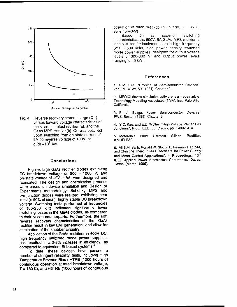
250
200-
150
100
2 2.5
Forward Voltage @ 8A (Volts)
Fig. 4. Reverse recovery stored charge (Qrr) versus forward voltage characteristics of the silicon ultrafast rectifier (a), and the GaAs MPS rectifier (b). Qrr was obtained upon switching from on-state current of 8A to reverse voltage of 400V, at di/dt~108A/s
Conclusions
High voltage GaAs rectifier diodes exhibiting DC breakdown voltage of 500 - 1000 V, and on-state voltage of ~2V at 8A, were designed and fabricated. The design and optimization process were based on device simulation and Design of Experiments methodology. Schottky, MPS, and p-n junction diodes were realized, exhibiting near ideal (> 90% of ideal), highly stable DC breakdown voltage. Switching tests performed at frequecies of 100-250 kHz indicated significantly lower switching losses in the GaAs diodes, as compared to their silicon counterparts. Furthermore, the soft reverse recovery characteristics of the GaAs rectifier result in low EMI generation, and allow for elimination of the snubber circuitry.
Application of the GaAs rectifiers in 400V DC, high frequency switched mode power supplies, has resulted in a 2-5% increase in efficiency, as compared to equivalent Si-based systems.6
To date, these devices have passed a number of stringent reliability tests, including High Temperature Reverse Bias/ HTRB (1000 hours of continuous operation at rated breakdown voltage, T = 150 C), and H3TRB (1000 hours of continuous
operation at rated breakdown voltage, T = 85 C. 85% humidity).
Based on its superior switching characteristics, the 600V, 8A GaAs MPS rectifier is ideally suited for implementation in high frequency (250 - 500 kHz), high power density switched mode power supplies, designed for output voltage levels of 300-600 V, and output power levels ranging to ~5 kW.
References
1. S.M. Sze, "Physics of Semiconductor Devices", 2nd Ed., Wiley, NY (1981), Chapter 2.
2. MEDICI device simulation software is a trademark of Technology Modeling Associates (TMA), Inc., Palo Alto, California.
3. B. J. Baliga, Power Semiconductor Devices, PWS, Boston (1996), Chapter 3.
4. Y.C. Kao, and E.D. Wolley, "High Voltage Planar P-N Junctions", Proc. IEEE, 55, (1967), pp. 1409-1414.
5. Motorola's # MURH860.
600V Ultrafast Silicon Rectifier,
6. Ali S.M. Salih, Ronald W. Slocumb, Peyman Hadizad, and Christine Thero, "GaAs Rectifiers for Power Supply and Motor Control Applications", in Proceedings, 10l
IEEE Applied Power Electronics Conference, Dallas, Texas (March, 1995).
38
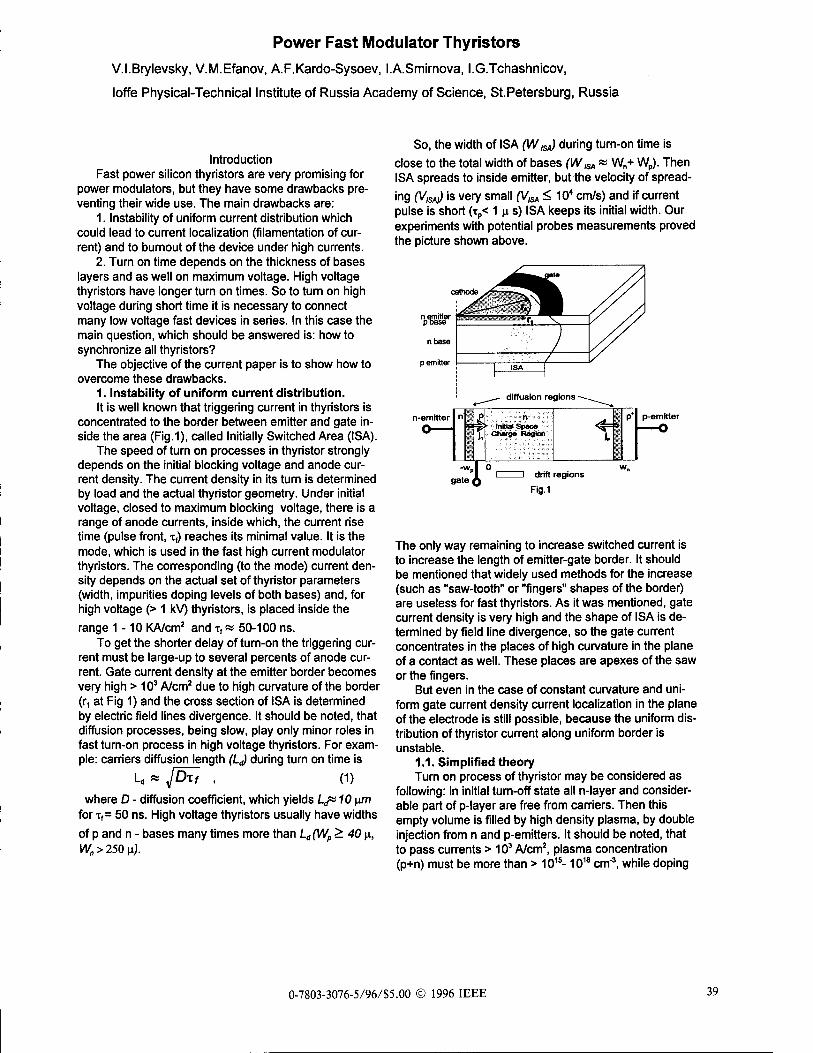
Power Fast Modulator Thyristors
V.I.Brylevsky, V.M.Efanov, A.F.Kardo-Sysoev, I.A.Smirnova, I.G.Tchashnicov,
loffe Physical-Technical Institute of Russia Academy of Science, StPetersburg, Russia
Introduction Fast power silicon thyristors are very promising for
power modulators, but they have some drawbacks pre- venting their wide use. The main drawbacks are:
1. Instability of uniform current distribution which could lead to current localization (filamentation of cur- rent) and to burnout of the device under high currents.
2. Turn on time depends on the thickness of bases layers and as well on maximum voltage. High voltage thyristors have longer turn on times. So to turn on high voltage during short time it is necessary to connect many low voltage fast devices in series. In this case the main question, which should be answered is: how to synchronize all thyristors?
The objective of the current paper is to show how to overcome these drawbacks.
1. Instability of uniform current distribution. It is well known that triggering current in thyristors is
concentrated to the border between emitter and gate in- side the area (Fig.1), called Initially Switched Area (ISA).
The speed of turn on processes in thyristor strongly depends on the initial blocking voltage and anode cur- rent density. The current density in its turn is determined by load and the actual thyristor geometry. Under initial voltage, closed to maximum blocking voltage, there is a range of anode currents, inside which, the current rise time (pulse front, tf) reaches its minimal value. It is the mode, which is used in the fast high current modulator thyristors. The corresponding (to the mode) current den- sity depends on the actual set of thyristor parameters (width, impurities doping levels of both bases) and, for high voltage (> 1 kV) thyristors, is placed inside the range 1-10 KA/cm2 and t,« 50-100 ns.
To get the shorter delay of turn-on the triggering cur- rent must be large-up to several percents of anode cur- rent. Gate current density at the emitter border becomes very high > 103 A/cm2 due to high curvature of the border (r, at Fig 1) and the cross section of ISA is determined by electric field lines divergence. It should be noted, that diffusion processes, being slow, play only minor roles in fast turn-on process in high voltage thyristors. For exam- ple: carriers diffusion length (LJ during turn on time is
Ld * JCfrf , (1)
where D - diffusion coefficient, which yields Lju 10 \im for T,= 50 ns. High voltage thyristors usually have widths of p and n - bases many times more than Ld(Wp > 40 n, Wn>250ii).
So, the width of ISA (WISA) during turn-on time is close to the total width of bases (WISA « W„+ Wp). Then ISA spreads to inside emitter, but the velocity of spread- ing (VISA)) is very small (V,SA < 104 cm/s) and if current pulse is short (tp< 1ns) ISA keeps its initial width. Our experiments with potential probes measurements proved the picture shown above.
diffusion regions -
n-omltter
Iff n
initial Spac» Charge Region
p-emitter
-wpl 0 gate A i i drift regions
Fig.1
The only way remaining to increase switched current is to increase the length of emitter-gate border. It should be mentioned that widely used methods for the increase (such as "saw-tooth" or "fingers" shapes of the border) are useless for fast thyristors. As it was mentioned, gate current density is very high and the shape of ISA is de- termined by field line divergence, so the gate current concentrates in the places of high curvature in the plane of a contact as well. These places are apexes of the saw or the fingers.
But even in the case of constant curvature and uni- form gate current density current localization in the plane of the electrode is still possible, because the uniform dis- tribution of thyristor current along uniform border is unstable.
1.1. Simplified theory Turn on process of thyristor may be considered as
following: in initial turn-off state all n-layer and consider- able part of p-layer are free from carriers. Then this empty volume is filled by high density plasma, by double injection from n and p-emitters. It should be noted, that to pass currents > 103 A/cm2, plasma concentration (p+n) must be more than > 1015-1018 cm3, while doping
0-7803-3076-5/96/S5.00 © 1996 IEEE 39
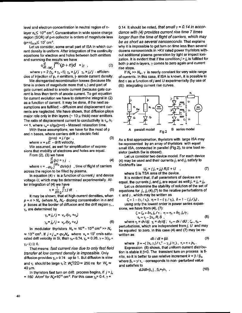
level and electron concentration in neutral region of n-
layer nn< 1014 cm3. Concentration in wide space charge region (SCR) of p-n collector is orders of magnitude less
(p+n)SCR< 107cm-3. Let us consider, some small part of ISA in which cur-
rent density is uniform. After integration of the continuity equations for electron and holes between both emitters and summing the results we have
where y = 2(yp+y„ -1), yp =j/j y„ =j/j - efficien- cies of injection of p, n emitters, j- anode current density.
We disregarded recombination losses (because life time is orders of magnitude more that x, ) and part of gate current added to anode current (because gate cur- rent is less than tenth of anode current. To get equation for current evolution we have to determine integral in (2) as a function of current. It may be done, if the next as- sumptions are fulfilled: - diffusion and displacement cur- rents are neglected. We have shown, that diffusion plays major role only in thin layers (~ 10 JJ. thick) near emitters. The ratio of displacement current to conductivity is xm /x, « 1, where xm= e/qu(p+n) - Maxwell relaxation time.
With these assumptions, we have for the most of p and n bases, where carriers drift in electric field
(p+n) =j/qv , (3) where v = \iE - drift velocity. We assumed, as well for simplification of expres-
sions that mobility of electrons and holes are equal. From (2), (3) we have
flVn (4)
where x = _wp J dx/v(x) , time of flight of carriers across the region to be filled by plasma.
In equation (4) x is a function of current ;' and device voltage U, which may be determined experimentally. Af- ter integration of (4) we have
*-i»0JW • (5) It may be shown, that at high current densities, when
p = n> NA (where N„, NA- doping concentration in n and p bases at the border of diffusion and the drift region yv. yp are determined by
Y„=//;'= v„/(vn*v^
yp=jp/j= Vp/fy+Vn) (6)
In modulator thyristors A/A« 1016- 1015cm"3 » /V„
« 1014cm2. If ;' <;'„= qVsN* where v, = 107cm/s satu- rated drift velocity in Si, than y„= 0.74, yp = 0.26, y = 2(yp +
Yn-0=0. That means: fast current rise due to only fast field
transfer at low current density is impossible. Only diffusion provides y„> 0.74 up to 1. But diffusion is slow
and x, should be large xf > W//2D » 250 ns for Wp« 40 urn.
In thyristors fast turn on drift process begins, if j >js
= 160 A/cm?for A/^IO14 cm3. For this case yp= 0.4, y =
0.14. It should be noted, that small y = 0.14 in accor- dance with (4) provides current rise time 7 times longer than the time of flight of carriers, which may be as short as several nanoseconds. That explains why it is impossible to get turn on time less than several dozens nanoseconds in >KV rated power thyristors with- out additional plasma generation by light or impact ioni- zation. It is evident that if the condition; >js is fulfilled for both p and n-layers, y comes to zero again and current rise stops.
If N, » Nd„ y is nearly constant for very wide range of currents. In this case, if ISA is known, it is possible to find x as a function of ;' and U experimentally (by use of (6)) integrating current rise curves.
A paralell model B series model
As a first approximation, thyristors with large ISA may be represented by an array of thyristors with equal small ISA, connected in parallel (Fig.2), to one load re- sistor (switch Sw is closed).
Let us consider two device model. For each device (4) may be used and their currents;, and;2 satisfy to Kirchhoffs law
U0 = (Ji+J2)R,S + U , (7) where S is TSA area of the device. It is evident that, if all parameters of devices are
equal, the currents;', and;2 are equal as well;', =;2 =;0. Let us determine the stability of solution of the set of
equations for ;',, ;2 (4),(7) to the relative perturbations of x and y, which may be written as
;=l-(x,/x2), TI = l-(y,/y2), 8 = 1-(;',/;,), using only the lowest order in power series expan-
sions, we have from (4), (7): C, = Cß + 8x„;0 /x; T| = T|O + H kh \
x0 = Tj-2xuRlS , (8) wherex, = dx/d;; yy = oV/d;'; xu =(h/dU;Co,T|0-
perturbations, which are independent from;, U and may be equaled to zero. In this case (4) and (7) may be re- written as:
dS/df = ß8 (9) where ß = -(2x0 y;'/x+
2 - yy;7x+), x+= x +/x0. Expression (8) shows, that uniform current distribu-
tion is stable it ß<0. The transient turn on process is fi- nite, so it is better to use relative increment k = ß / ß„, where ß0 = y/ x+ - corresponds to non- perturbed value and satisfies to
dJ/dr=ß0.j, ß0=y/x+ . (10)
40
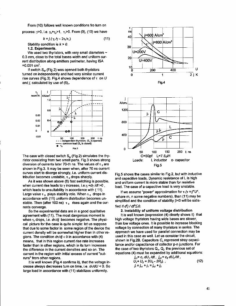
From (10) follows well known conditions fro turn on
process: y>0, i.e. y„+yp>1, T+>0. From (9), (10) we have
fr=y(Y,A-2To/T+)
Stability condition is k > 0.
(11)
1.2. Experiments. We used two thyristors, with very small diameters ~
0.3 mm, close to the total bases width and uniform cur- rent distribution along emitters perimeter, having ISA =0.001 cm2.
If switch Sw (Fig.2) was opened both thyristors turned on independently and had very similar current rise curves (Fig.3). Fig.4 shows dependence of x on U and j, calculated by use of (5),.
1
Fig.4
2 j K
nscmVA
0.03
0.02
0.01
0
-0.01
i KA/cm2
1 2
t *.
._ jl'
1
0.8
f 1 , - — "
jV 1 I \ 1 / •
0.4
\ / II ' u t//7 ' -Ja
Ojj w * 1
oo
50 100 150 200 t ns independent thyristors (S. is opened) common load (S. Is closed) © to
Fln.3
The case with closed switch Sw (Fig.2) simulates the thy- ristor consisting from two small parts. Fig.3 shows strong diversion of currents later 70-th ns. The values of T 0 are shown in Fig.3. It may be seen when, after 70 ns current curves start to diverge strongly, i.e. uniform current dis- tribution becomes unstable, T 0 drops sharply.
As it was shown above (6) fast switching is possible, when current rise leads to y increase, i.e.y, =dy/df >0 , which leads to unsuitability in accordance with (11). Large value T 0 plays stability role. When T 0 drops in accordance with (11) uniform distribution becomes un- stable. Then (after 100 ns) T 0 rises again and the cur- rents converge.
So the experimental data are in a good qualitative agreement with (11). The most dangerous moment is when T0 drops, i.e. (k/dj becomes negative. The physi- cal picture for the case is quite simple: let us suppose that due to some factor in some region of the device the current density will be somewhat higher than in other re- gions. The condition ch/dj < 0 in accordance with (4) means, that in this region current rise rate increases faster than in other regions, which in its turn increases the difference in the current densities and so on. The current in the region with initial excess of current "out- runs" from other regions.
It is well known (Fig.4 confirms it), that the voltage in- crease always decreases turn on time, i.e. dx/dU < 0. So large load in accordance with (11) stabilizes uniformity.
J A/cm
120Ü
800
400
V \ I c
L Y^A
^y* C
50 100 150 200 t ns C=50pf L=7.5nH
Loads: L inductor c- capacitor
Fig.5
Fig.5 shows the cases similar to Fig.2, but with inductive and capacitive loads. Dynamic resistance of L is high and uniform current is more stable than for resistive load. The case of a capacitive load is very unstable.
If we assume "power" approximation for T (X «/"(/•, where m, n some negative numbers), than (11) may be simplified and the condition of stability ß<0 will be satis-
fied if cPj/df<0. 2. Instability of uniform voltage distribution It is well known (expression (4) clearly shows it) that
high voltage thyristors having wide bases are slower, than low voltage ones. It is possible to increase blocking voltage by connection of many thyristors in series. The approach we have used for parallel connection may be used in this case as well. Let us consider the circuit, shown in Fig.2B. Capacitors C„ represent stray capaci- tance and/or capacitance of collector p-n junctions. For the case of two thyristors Q,, Q2 the previous set of equations (4) must be expanded by additional equations:
jc1= c, dU, tdt, jc2 = c2 dU2/dt, U1+U2 = 2U0-2R,jl , (12) Jl=jc1+Jl=jc2+J2
41
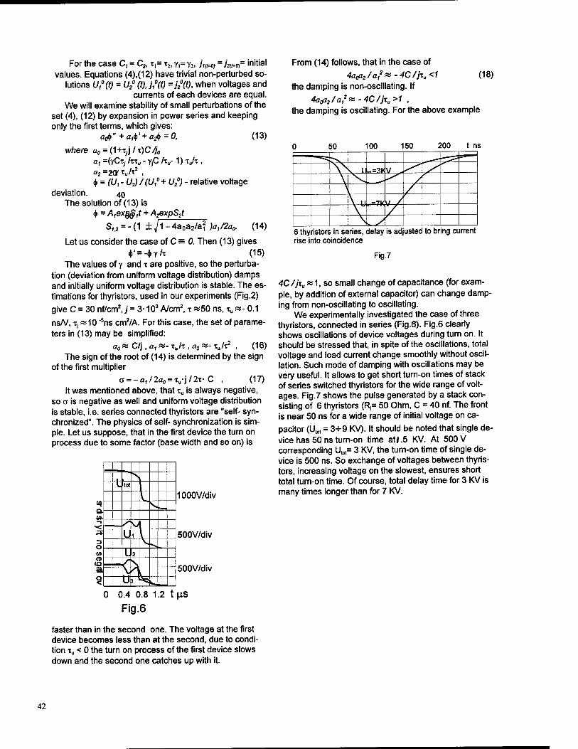
For the case C, = C2, T,= T2, YI= y2, JKM» =h^ar initial values. Equations (4),(12) have trivial non-perturbed so-
lutions Ufft) = U2° (t), U°(t) =h°(t), when voltages and currents of each devices are equal.
We will examine stability of small perturbations of the set (4), (12) by expansion in power series and keeping only the first terms, which gives:
aA"+atf+aA=0, (13)
where a0 = (1 +tyj li)C/jB
a-, =(YCT, /TT„ - YjC hu-1) xjx, a2
=20/T„/T2 , ^ = (Ui- UJ/tU,0* U2°) - relative voltage
deviation. 40 The solution of (13) is
4> = ^,ex§£,f + A2expSjt
Sr2 = -(1 ±^1-4a0a2/a?M/2fl0. (14)
Let us consider the case of C = 0. Then (13) gives f = -4>y/i (15)
The values of y and T are positive, so the perturba- tion (deviation from uniform voltage distribution) damps and initially uniform voltage distribution is stable. The es- timations for thyristors, used in our experiments (Fig.2)
give C = 30 nf/cm2,;' = 3-103 A/cm2, T «50 ns, tu»- 0.1
ns/V, Tj «10 "'ns cm2/A. For this case, the set of parame- ters in (13) may be simplified:
a0 » C/j, a, «- TU/T , a2 »- TU/T2 , (16)
The sign of the root of (14) is determined by the sign of the first multiplier
a = -a,/2a0 = Tu-j/2T-C , (17) It was mentioned above, that TU is always negative,
so a is negative as well and uniform voltage distribution is stable, i.e. series connected thyristors are "self- syn- chronized". The physics of self- synchronization is sim- ple. Let us suppose, that in the first device the turn on process due to some factor (base width and so on) is
1000V/div
="—-> ̂ L licit
_L «I _ ^ —1 —s\ J 3 Ui _L_ 3 >^ CO I2 (l> (Q -c\ V tik V L Ü 05 :^_
500V/div
500V/div
0 0.4 0.8 1.2 t U.S
Fig.6
faster than in the second one. The voltage at the first device becomes less than at the second, due to condi- tion xu < 0 the turn on process of the first device slows down and the second one catches up with it.
From (14) follows, that in the case of
4a0a2/a,2«-4C//ru<-/ (18) the damping is non-oscillating. If
4a0a2/a12&-4C/fzu>1 ,
the damping is oscillating. For the above example
150 200 t ns
6 thyristors in series, delay is adjusted to bring current rise into coincidence
Fig.7
4C//ru «1, so small change of capacitance (for exam- ple, by addition of external capacitor) can change damp- ing from non-oscillating to oscillating.
We experimentally investigated the case of three thyristors, connected in series (Fig.6). Fig.6 clearly shows oscillations of device voltages during turn on. It should be stressed that, in spite of the oscillations, total voltage and load current change smoothly without oscil- lation. Such mode of damping with oscillations may be very useful. It allows to get short turn-on times of stack of series switched thyristors for the wide range of volt- ages. Fig.7 shows the pulse generated by a stack con- sisting of 6 thyristors (R,= 50 Ohm, C = 40 nf. The front is near 50 ns for a wide range of initial voltage on ca-
pacitor (Utot = 3-^9 KV). It should be noted that single de- vice has 50 ns turn-on time atl.5 KV. At 500 V corresponding U,o,= 3 KV, the turn-on time of single de- vice is 500 ns. So exchange of voltages between thyris- tors, increasing voltage on the slowest, ensures short total turn-on time. Of course, total delay time for 3 KV is many times longer than for 7 KV.
42
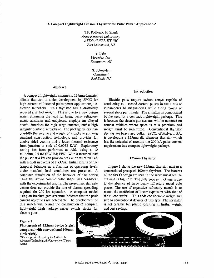
A Compact Lightweight 125 mm Thyristor for Pulse Power Applications*
T.F. Podlesak, H. Singh Army Research Laboratory
ATTN: AMSRL-WT-NH Fort Monmouth, NJ
S. Behr Vitronics, Inc. Eatontown, NJ
S. Schneider Consultant
Red Bank, NJ
Abstract
A compact, lightweight, symmetric 125mm diameter silicon thyristor is under development by SPCO for high current millisecond pulse power applications, i.e. electric launchers. This thyristor has a drastically reduced size and weight. This is due to a new design which eliminates the need for large, heavy refractory metal substrates and endpieces, employs an alloyed anode interface for high surge currents, and a high integrity plastic disk package. The package is less than one-fifth the volume and weight of a package utilizing standard construction technology, and provides for double sided cooling and a lower thermal resistance from junction to sink of 0.0033 K/W. Exploratory testing has been performed at ARL using a 10 milliohm, 0.5 ms (FWHM) PFN. With a matched load the pulser at 4 kV can provide peak currents of 200 kA with a di/dt in excess of 1 kA/us. Initial results on the temporal behavior as a function of operating levels under matched load conditions are presented. A computer simulation of the behavior of the device using the actual current pulse shape was consistent with the experimental results. The present six star gate design does not provide the rate of plasma spreading required for 200 kA operation. A computer model using an involute gate structure indicates that the peak current objectives are achievable. The development of this switch will permit the construction of compact, lightweight high voltage series switch stacks for electric guns.
Figure 1 Photograph of 125mm device (right), compared with conventional 100mm device(left). *Work supported in part by the Institute for Advanced Technology, the University of Texas, Austin
Introduction
Electric guns require switch arrays capable of conducting millisecond current pulses in the 100's of kiloamperes to megamperes while firing bursts of several shots per minute. The situation is complicated by the need for a compact, lightweight package. This is because the electric gun systems will be mounted on combat vehicles where space is at a premium and weight must be minimized. Conventional thyristor designs are heavy and bulky. SPCO, of Malvern, PA, is developing a 125mm die diameter thyristor which has the potential of meeting the 200 kA pulse current requirement in a compact lightweight package.
125mm Thyristor
Figure 1 shows the new 125mm thyristor next to a conventional presspack 100mm thyristor. The features of the SPCO design are seen in the mechanical outline drawing in Figure 2. The difference in thickness is due to the absence of large heavy refractory metal pole pieces. The use of expensive refractory metals is to match the coefficient of linear expansion with that of the silicon wafer. This adds considerable weight and size to conventional devices of this type. The insulator is not ceramic but plastic resulting in further weight and cost savings.
0-7803-3076-5/96/S5.00 © 1996 IEEE 43
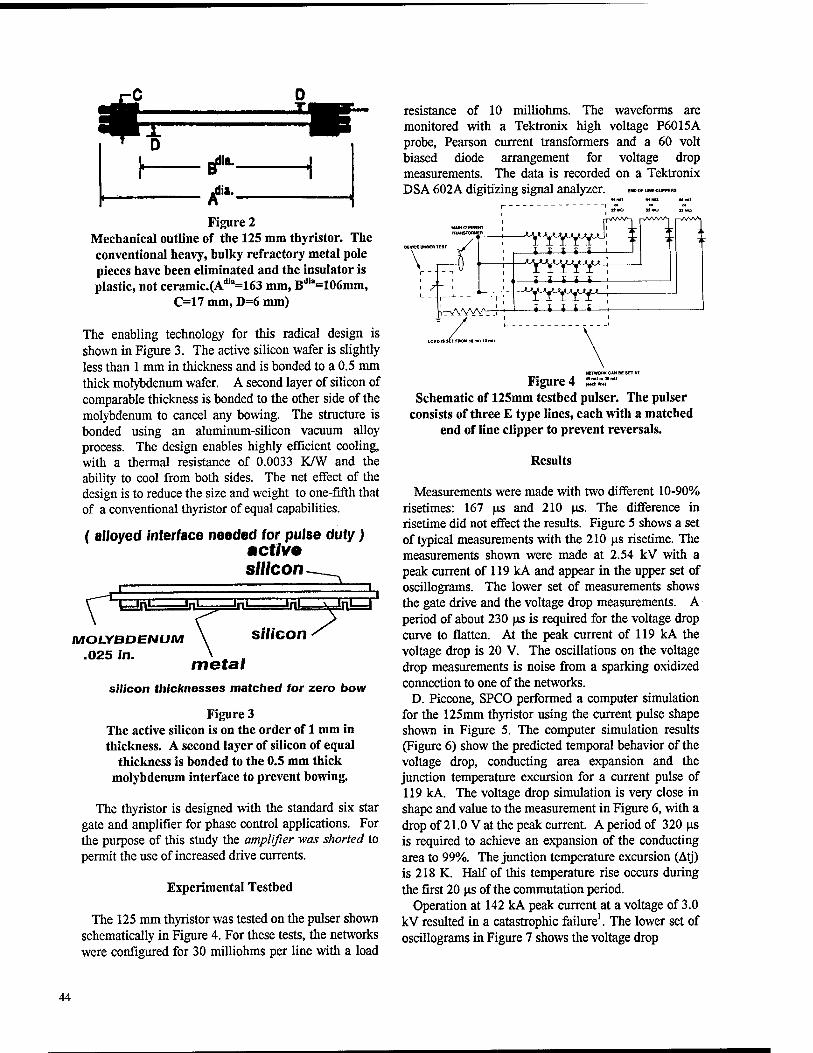
* T D
la.
n.
Figure 2 Mechanical outline of the 125 mm thyristor. The conventional heavy, bulky refractory metal pole pieces have been eliminated and the insulator is plastic, not ceramic.(Adia=163 mm, Bdia=106mm,
C=17 mm, D=6 mm)
The enabling technology for this radical design is shown in Figure 3. The active silicon wafer is slightly less than 1 mm in thickness and is bonded to a 0.5 mm thick molybdenum wafer. A second layer of silicon of comparable thickness is bonded to the other side of the molybdenum to cancel any bowing. The structure is bonded using an aluminum-silicon vacuum alloy process. The design enables highly efficient cooling, with a thermal resistance of 0.0033 K/W and the ability to cool from both sides. The net effect of the design is to reduce the size and weight to one-fifth that of a conventional thyristor of equal capabilities.
( alloyed interface needed for pulse duty J active silicon ^__
r BnE 3KE 3HE 3nE
MOLYBDENUM .025 in.
silicon
5Q~
metal silicon thicknesses matched for zero bow
Figure 3 The active silicon is on the order of 1 mm in thickness. A second layer of silicon of equal
thickness is bonded to the 0.5 mm thick molybdenum interface to prevent bowing.
The thyristor is designed with the standard six star gate and amplifier for phase control applications. For the purpose of this study the amplifier was shorted to permit the use of increased drive currents.
Experimental Testbed
The 125 mm thyristor was tested on the pulser shown schematically in Figure 4. For these tests, the networks were configured for 30 milliohms per line with a load
resistance of 10 milliohms. The waveforms are monitored with a Tektronix high voltage P6015A probe, Pearson current transformers and a 60 volt biased diode arrangement for voltage drop measurements. The data is recorded on a Tektronix DSA 602A digitizing signal analyzer. ENO OF LINE CUPPERS
DEVICE UNDER TI
\
rAW:
t i t t t
—i t t t t
—i i * i i
12 mO 12 mt;
10*0 IS Mt fROM 11 irtfl 10 mi
Figure 4 Schematic of 125mm testbed pulser. The pulser
consists of three £ type lines, each with a matched end of line clipper to prevent reversals.
Results
Measurements were made with two different 10-90% risetimes: 167 us and 210 us. The difference in risetime did not effect the results. Figure 5 shows a set of typical measurements with the 210 JJ.S risetime. The measurements shown were made at 2.54 kV with a peak current of 119 kA and appear in the upper set of oscillograms. The lower set of measurements shows the gate drive and the voltage drop measurements. A period of about 230 us is required for the voltage drop curve to flatten. At the peak current of 119 kA the voltage drop is 20 V. The oscillations on the voltage drop measurements is noise from a sparking oxidized connection to one of the networks.
D. Piccone, SPCO performed a computer simulation for the 125mm thyristor using the current pulse shape shown in Figure 5. The computer simulation results (Figure 6) show the predicted temporal behavior of the voltage drop, conducting area expansion and the junction temperature excursion for a current pulse of 119 kA. The voltage drop simulation is very close in shape and value to the measurement in Figure 6, with a drop of 21.0 V at the peak current. A period of 320 u.s is required to achieve an expansion of the conducting area to 99%. The junction temperature excursion (Atj) is 218 K. Half of this temperature rise occurs during the first 20 pis of the commutation period.
Operation at 142 kA peak current at a voltage of 3.0 kV resulted in a catastrophic failure1. The lower set of oscillograms in Figure 7 shows the voltage drop
44
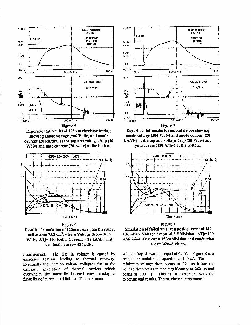
4.5kV
500V /div
!not! trig 'd
LI
2.54 kV
PEAK CURRENT 119 kA
Ii i■iIti i i I i ''» I i ■ i i
100us/div
100JUS/dlv 900U3
Figure 5 Experimental results of 125mm thyristor testing,
showing anode voltage (500 V/div) and anode current (20 kA/div) at the top and voltage drop (10 V/div) and gate current (20 A/div) at the bottom.
delta Tj
Tine (sec)
Figure 6 Results of simulation of 125mm, star gate thyristor,
active area 75.2 cm2, where Voltage drop= 10.5 V/div, ATj= 100 K/div, Current = 35 kA/div and
conduction area= 45%/div.
measurement. The rise in voltage is caused by excessive heating, leading to thermal runaway. Eventually the junction voltage collapses due to the excessive generation of thermal carriers which overwhelm the normally injected ones causing a funneling of current and failure. The maximum
4.5kV —-—i 1 1 —«
3.0 kV
, —r- 1 1
PEAK CURRENT 142 kA
RISETIME 110-90X)
\ 210 us 500V /dlv
I not! trig'd
LI
Rnov ■ ■
-IOOJJS 100us/div
90V
10V /div m
!not! trig'd
LI
-lov -IOOJJS lOOus/div
Figure 7 Experimental results for second device showing anode voltage (500 V/div) and anode current (20
kA/div) at the top and voltage drop (10 V/div) and gate current (20 A/div) at the bottom.
9001J3
t delta Ij
Tine (sec)
Figure 8 Simulation of failed unit at a peak current of 142
kA. where Voltage drop= 10.5 V/division, ATj= 100 K/division, Current = 35 kA/division and conduction
area= 36%/division.
voltage drop shown is clipped at 60 V. Figure 8 is a computer simulation of operation at 145 kA. The minimum voltage drop occurs at 220 us before the voltage drop starts to rise significantly at 260 us and peaks at 390 us. This is in agreement with the experimental results. The maximum temperature
45
Figure 9 Photograph of interior of failed thyristor.
excursion is 363 K. The failed device was opened and photographed (Figure 9). The points where melting occurred during the thermal runaway and the fracture caused by the large temperature excursions are noted. This failure is caused by the slow rate of plasma expansion with the six star gate design.
In prior experiments with 4500 V SPCO2 100mm thyristors with an involute gate design, we achieved peak current capabilities of 150 kA. A computer simulation of the 5000 V 125mm thyristor with an involute gate was performed at a peak current of 200 kA. The conducting emitter area was reduced by theincreased size of the gate from 75.2 cm2 to 66.9 cm2. The results in Figure 10 show a dramatic change in the performance of the thyristor. The rate of area expansion has increased by greater than a factor of three with 100% of the conduction area achieved in 100 us, where before it required 320 us to obtain 99% conduction area at 119 kA with the six star gate configuration.. The total temperature excursion is 169 K at 200 kA compared to 218 K at 119 kA(star gate). The commutation temperature rise of 45 K during the first 20 us is less than one-half of the 110 K rise at 119 kA(star gate).
Conclusions
SPCO has successfully developed a new mechanical design for building a 125mm thyristor which reduces volume and weight to one-fifth of a conventional press pack design. The initial devices were constructed with
de It« Tj
line (sec)
Figure 10 Computer simulation of device performance at 200
kA where Voltage drop= 10.5 V/div, ATj= 100 K/div, Current = 35 kA/div and conduction area=
36%/div.
the six star gate design used for phase control applications. The high current pulse performance of these devices was evaluated in a 0.5 ms pulser. Experimental peak current operation and limitations experimentally determined were in agreement with computer simulations performed at SPCO. The six star gate design provided an inadequate rate of plasma expansion. A computer simulation with an appropriately scaled involute gate design which had been used successfully in a prior investigation on 100mm thyristors showed that reliable 200 kA pulse current is achievable. Further studies will be performed with the new gate design.
Acknowledgment
The authors wish to express their appreciation to Dr. H. Mehta, W. Tobin and D. Piccone of SPCO, Malvern, PA for their significant contributions to this paper.
Reference
1. I. Somos et al., "Power Semiconductors-Empirical Diagrams Expressing Life as a Function of Temperature Excursion", IEEE Transactions on Magnetics, 29, January 1993, Part II, pp. 517-522 2. R Pastore, L. Kingsley, H. Singh, S. Schneider, G. Ayres,"Reverse Blocking Capability of Symmetric SCRs at High Current and High Voltage Reversals," Proceedings of the 10th IEEE Pulsed Power Conference, Albuquerque, NM, July 1995,.
46
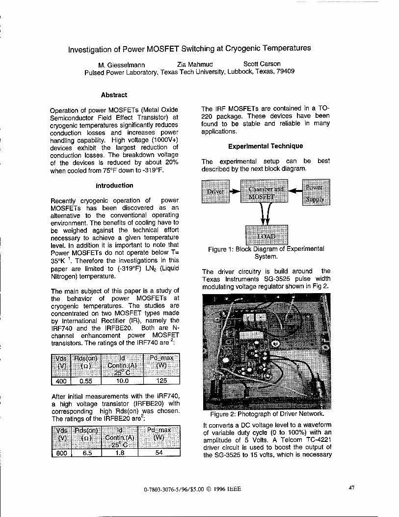
Investigation of Power MOSFET Switching at Cryogenic Temperatures
M. Giesselmann Zia Mahmud Scott Carson Pulsed Power Laboratory, Texas Tech University, Lubbock, Texas, 79409
Abstract
Operation of power MOSFETs (Metal Oxide Semiconductor Field Effect Transistor) at cryogenic temperatures significantly reduces conduction losses and increases power handling capability. High voltage (1000V+) devices exhibit the largest reduction of conduction losses. The breakdown voltage of the devices is reduced by about 20% when cooled from 75°F down to -319°F.
Introduction
Recently cryogenic operation of power MOSFETs has been discovered as an alternative to the conventional operating environment. The benefits of cooling have to be weighed against the technical effort necessary to achieve a given temperature level. In addition it is important to note that Power MOSFETs do not operate below T= 35°K 1. Therefore the investigations in this paper are limited to (-319°F) LN2 (Liquid Nitrogen) temperature.
The main subject of this paper is a study of the behavior of power MOSFETs at cryogenic temperatures. The studies are concentrated on two MOSFET types made by International Rectifier (IR), namely the IRF740 and the IRFBE20. Both are N- channel enhancement power MOSFET transistors. The ratings of the IRF740 are 2:
Vds (V)
Rds(on) (o)
Id Contin.(A)
25° C
Pd max (W)
400 0.55 10.0 125
After initial measurements with the IRF740, a high voltage transistor (IRFBE20) with corresponding high Rds(on) was chosen. The ratings of the IRFBE20 are2:
Vds (V)
Rds(on) (a)
Id Contin.(A)
25° C
Pd max (W)
800 6.5 1.8 54
The IRF MOSFETs are contained in a TO- 220 package. These devices have been found to be stable and reliable in many applications.
Experimental Technique
The experimental setup can be described by the next block diagram.
best
Chamber and MOSFET
2 Power
Supply
LOAD
Figure 1: Block Diagram of Experimental System.
The driver circuitry is build around the Texas Instruments SG-3525 pulse width modulating voltage regulator shown in Fig 2.
Figure 2: Photograph of Driver Network.
It converts a DC voltage level to a waveform of variable duty cycle (0 to 100%) with an amplitude of 5 Volts. A Telcom TC-4221 driver circuit is used to boost the output of the SG-3525 to 15 volts, which is necessary
0-7803-3076-5/96/S5.00 © 1996 IEEE 47
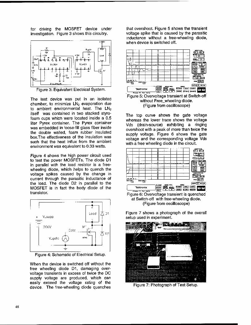
for driving the MOSFET device under investigation. Figure 3 shows this circuitry.
Cbul
Jo. 4-Sv/
, VA- 10V
+ 1SV
ft ft ft 4 ft fi ft ? i CA.3521
Ht < 10k > :
-i TC_4421
i Lood
Figure 3: Equivalent Electrical System.
The test device was put in an isolated chamber, to minimize LN2 evaporation due to ambient environmental heat. The LN2
itself was contained in two stacked styro- foam cups which were located inside a 0.5 liter Pyrex container. The Pyrex container was embedded in loose-fill glass fiber inside the double walled, foam rubber insulated box.The effectiveness of the insulation was such that the heat influx from the ambient environment was equivalent to 0.33 watts.
Figure 4 shows the high power circuit used to test the power MOSFETs. The diode D1 in parallel with the load resistor is a free- wheeling diode, which helps to quench the voltage spikes caused by the change in current through the parasitic inductance of the load. The diode D2 in parallel to the MOSFET is in fact the body diode of the transistor.
Figure 4: Schematic of Electrical Setup.
When the device is switched off without the free wheeling diode D1, damaging over- voltage transients in excess of twice the DC supply voltage are produced, which can easily exceed the voltage rating of the device. The free-wheeling diode quenches
that overshoot. Figure 5 shows the transient voltage spike that is caused by the parasitic inductance without a free-wheeling diode, when device is switched off.
TV III 11 1 ' ;' ' / /^
I \ / i
13.84 u s
WEBTICJI- EO Bra »2233
IBTOBE] | WCQ | |CUBB|
IT] r« lf«1 IBHOMI EISPLJ hooen I
Figure 5: Overvoltage transient at Switch-off without Free_wheeling diode.
(Figure from oscilloscope)
The top curve shows the gate voltage whereas the lower trace shows the voltage Vds (drain-source) exhibiting a ringing overshoot with a peak of more than twice the supply voltage. Figure 6 shows the gate voltage and the corresponding voltage Vds with a free wheeling diode in the circuit.
CiBB —TRieeea—■
f^-H LEVEL
1 1 \ r 1
13.84 U N
HORIZONT M.
ICLE^tl SAUE/ttCI. |ftUTo(_*JB
STORE] | ftCB | ICURSI
ff) [ • II • I I8HOMI Mapil MODEM!
Figure 6: Overvoltage transient is quenched at Switch-off with free-wheeling diode.
(Figure from oscilloscope)
Figure 7 shows a photograph of the overall setup used in experiment.
Figure 7: Photograph of Test Setup.
48
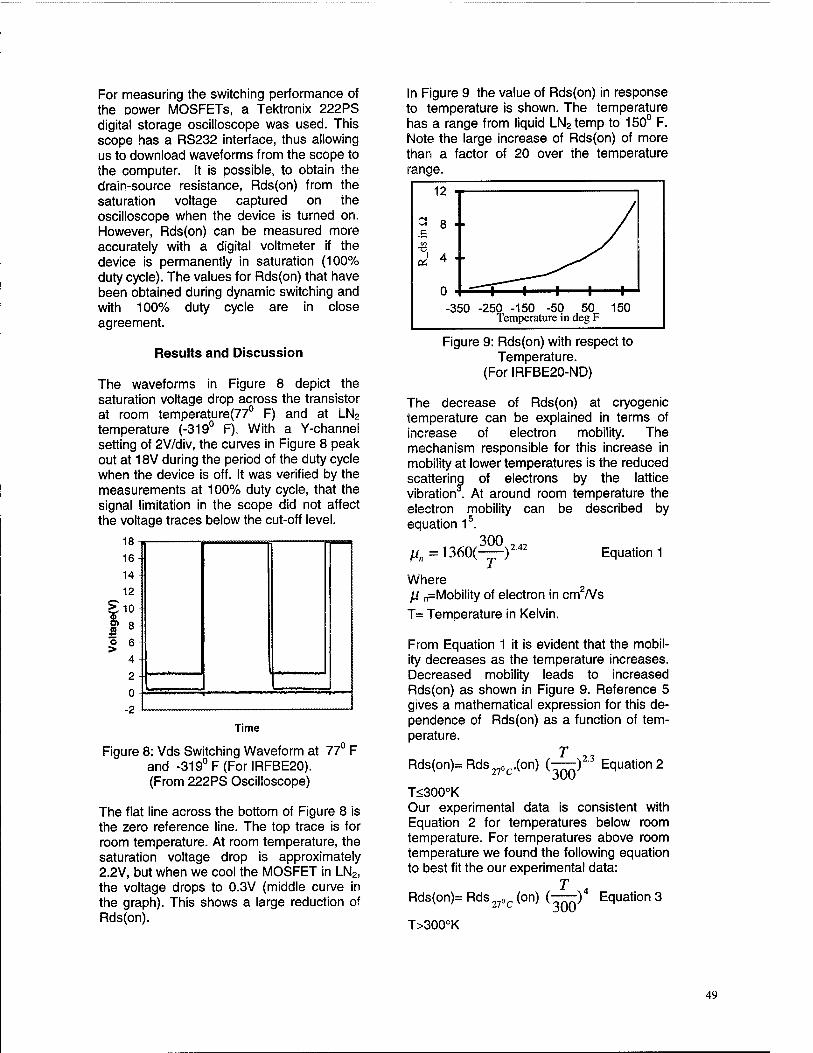
For measuring the switching performance of the power MOSFETs, a Tektronix 222PS digital storage oscilloscope was used. This scope has a RS232 interface, thus allowing us to download waveforms from the scope to the computer. It is possible, to obtain the drain-source resistance, Rds(on) from the saturation voltage captured on the oscilloscope when the device is turned on. However, Rds(on) can be measured more accurately with a digital voltmeter if the device is permanently in saturation (100% duty cycle). The values for Rds(on) that have been obtained during dynamic switching and with 100% duty cycle are in close agreement.
Results and Discussion
The waveforms in Figure 8 depict the saturation voltage drop across the transistor at room temperature(77° F) and at LN2
temperature (-319° F). With a Y-channel setting of 2V/div, the curves in Figure 8 peak out at 18V during the period of the duty cycle when the device is off. It was verified by the measurements at 100% duty cycle, that the signal limitation in the scope did not affect the voltage traces below the cut-off level.
IÖ -
16-
14-
12 -
> 10- o O) Q . ID °
o 6-
4-
2
0 - -9 -
Time
Figure 8: Vds Switching Waveform at 77° F and -319°F(ForlRFBE20). (From 222PS Oscilloscope)
The flat line across the bottom of Figure 8 is the zero reference line. The top trace is for room temperature. At room temperature, the saturation voltage drop is approximately 2.2V, but when we cool the MOSFET in LN2, the voltage drops to 0.3V (middle curve in the graph). This shows a large reduction of Rds(on).
In Figure 9 the value of Rds(on) in response to temperature is shown. The temperature has a range from liquid LN2temp to 150° F. Note the large increase of Rds(on) of more than a factor of 20 over the temperature range.
a a
* ■^ I 4 ■
0 ■ •—r~ —i— —i— —i— —*— -350 -250 -150 -50 50 150
Temperature in deg F
Figure 9: Rds(on) with respect to Temperature.
(For IRFBE20-ND)
The decrease of Rds(on) at cryogenic temperature can be explained in terms of increase of electron mobility. The mechanism responsible for this increase in mobility at lower temperatures is the reduced scattering of electrons by the lattice vibration . At around room temperature the electron mobility can be described by equation 15.
300 fin=l360(-—) 2.42 Equation 1
Where ß n=Mobility of electron in cm2/Vs
T= Temperature in Kelvin.
From Equation 1 it is evident that the mobil- ity decreases as the temperature increases. Decreased mobility leads to increased Rds(on) as shown in Figure 9. Reference 5 gives a mathematical expression for this de- pendence of Rds(on) as a function of tem- perature.
T )2'3 Equation 2 Rds(on)=Rds27„c.(on)(300
T<300°K Our experimental data is consistent with Equation 2 for temperatures below room temperature. For temperatures above room temperature we found the following equation to best fit the our experimental data:
T Rds(on)=Rds270c(on) (TTT)4 Equations
T>300°K
49
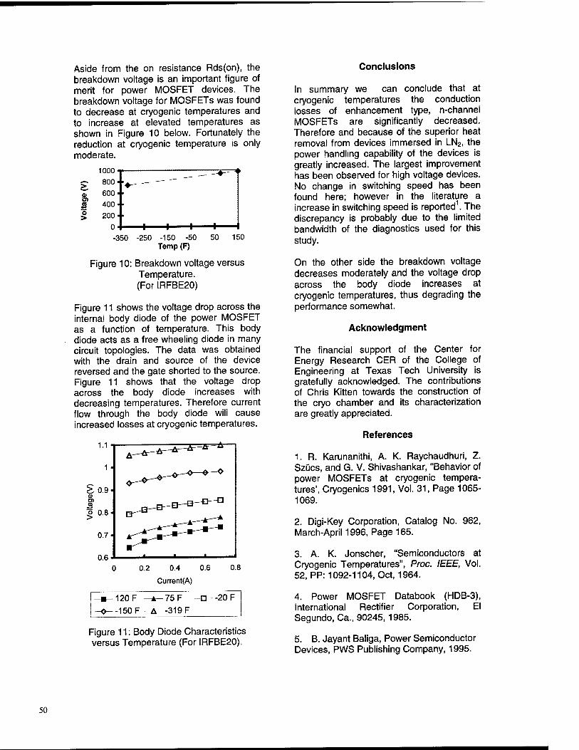
Aside from the on resistance Rds(on), the breakdown voltage is an important figure of merit for power MOSFET devices. The breakdown voltage for MOSFETs was found to decrease at cryogenic temperatures and to increase at elevated temperatures as shown in Figure 10 below. Fortunately the reduction at cryogenic temperature is only moderate.
1000
0) en £ o >
-350 -250 -150 -50 Temp (F)
150
Figure 10: Breakdown voltage versus Temperature. (For IRFBE20)
Figure 11 shows the voltage drop across the internal body diode of the power MOSFET as a function of temperature. This body diode acts as a free wheeling diode in many circuit topologies. The data was obtained with the drain and source of the device reversed and the gate shorted to the source. Figure 11 shows that the voltage drop across the body diode increases with decreasing temperatures. Therefore current flow through the body diode will cause increased losses at cryogenic temperatures.
0.2 0.4 0.6
Current(A)
120 F ^A-75F -Q—20 F
-150 F -A--319F
Figure 11: Body Diode Characteristics versus Temperature (For IRFBE20).
Conclusions
In summary we can conclude that at cryogenic temperatures the conduction losses of enhancement type, n-channel MOSFETs are significantly decreased. Therefore and because of the superior heat removal from devices immersed in LN2, the power handling capability of the devices is greatly increased. The largest improvement has been observed for high voltage devices. No change in switching speed has been found here; however in the literature a increase in switching speed is reported . The discrepancy is probably due to the limited bandwidth of the diagnostics used for this study.
On the other side the breakdown voltage decreases moderately and the voltage drop across the body diode increases at cryogenic temperatures, thus degrading the performance somewhat.
Acknowledgment
The financial support of the Center for Energy Research CER of the College of Engineering at Texas Tech University is gratefully acknowledged. The contributions of Chris Kitten towards the construction of the cryo chamber and its characterization are greatly appreciated.
References
1. R. Karunanithi, A. K. Raychaudhuri, Z. Szücs, and G. V. Shivashankar, "Behavior of power MOSFETs at cryogenic tempera- tures', Cryogenics 1991, Vol. 31, Page 1065- 1069.
2. Digi-Key Corporation, Catalog No. 962, March-April 1996, Page 165.
3. A. K. Jonscher, "Semiconductors at Cryogenic Temperatures", Proc. IEEE, Vol. 52, PP: 1092-1104, Oct, 1964.
4. Power MOSFET Databook (HDB-3), International Rectifier Corporation, El Segundo, Ca., 90245, 1985.
5. B. Jayant Baliga, Power Semiconductor Devices, PWS Publishing Company, 1995.
50
Power Nanosecond Semiconductor Opening Plasma Switches V.I.Brylevsky, V.M.Efanov, A.F.Kardo-Sysyev, I.G.Tchashnicov
loffe Physical - Technical Institute of Russian Academy of Russian Academy of Science, StPetersburg, Russia
Introduction Opening switches (OS) with inductive storage system
are very promising in Pulsed Power applications. The density of energy stored in an inductor is higher than in a capacitor. The pulsed voltage generated during a short time at the load may be many times (dozens) higher than the voltage at which the energy has been stored. In early 80-s a new effect of super fast voltage restoration in high voltage silicon p-n junctions, when the junction current is switched from forward to reverse direction, was discovered. This discovery gave rise to a new generation of solid state plasma opening switches, called Drift Step Recovery Diodes (DSRD) [1]. Being semiconductor de- vices, DSRD have unlimited life time, low jitter. Maximum repetition rate is limited mainly by heat and may be as high as megahertz.
In this work the performance of DSRD and their limits will be considered.
Consideration of general physics
Fig.l
Fast recovery of high voltage p-n junctions
When short forward current pulse (pumping) is ap- plied to p+nn+ structure (Fig.1, Fig.2), the plasma injec- tion process starts. Highly enriched by carriers, diffusion region appears near the p-n junction. The width of the re- gion (Wd) is
»> J2DX+ , (1) where D - diffusion coefficient, x+ - the pumping
pulse length. Part of the injected charge (equal to \np % p +n„),
where n p ,n„ - carriers mobility) is accumulated in a drift wave (Fig.2), which "head" propagates from diffusion re- gion into the n-layer with the velocity (Vf)
Vf=j+/qNd (2)
where /♦ - pumping current density, Nd - n-layer doping.
When the current changes direction into the reverse, the drift wave moves back with the velocity, determined by (2) as well. The drift region is being compressed.
Fig.2 Carriers and field distribution during recovery of high voltage p-n junctions
Near p-n junction in the diffusion region, the region of re- verse concentration gradient appears. When concentra- tion of electrons reaches zero level, neutrality condition can not be sustained longer and space charge region (SCR) arises. The rate of SCR voltage drop increase (dU/dt) is proportional to the velocity of the border of widening SCR (vSCR).
0-7803-3076-5/96/S5.00 © 1996 IEEE 51
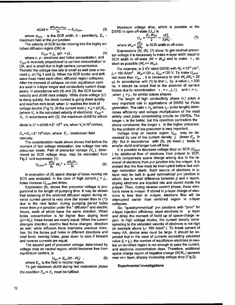
±_. qNdWscrVscr _ ,- dU/df« ^ E"
VSCR . (3)
where wSCR - is the SCR width, 8 - permitivity, Em - maximum field at the p-n junction.
The velocity of SCR border moving into the highly en- riched diffusion region (DR) is •
VSCR^L Q(n +P)> W where n, p - electrons and holes concentration, and
VSCR is inversely proportional to carriers concentration in DR, and is small due to high carriers concentration. Therefor the voltage rise rate is small as well (see a mo- ment f2 on Fig.1 and 2). When the SCR border and drift wave head meet each other, diffusion region collapses. After the moment of collapse, no non- equilibrium carri- ers exist in n-layer longer and conductivity current disap- pears. In accordance with (4) and (3), the SCR border velocity and dU/dt rises sharply. While diode voltage (U) is rising quickly, the diode current is going down quickly and reaches zero level, when U reaches the level of voltage source (Fig.1). At the current level j = js= qV^, (where Vs is the saturated velocity of electrons) VSCR = Vs. In accordance with (3), the maximum dU/dt for silicon
diode is U' = dU/dt&2' 1012 v/s, when Vs»107cm/sec,
£m«£a«2* fOVcm, where £a - breakdown field intensity.
The consideration made above shows that before the moment of fast voltage restoration, low voltage rise rate precursor exists. Part of precursor voltage (Vp ), deter- mined by SCR voltage drop, may be estimated from Fig.2 and expression (1).
qNd ,,. 2 _ q/VdOr-» u, 'pSCR* 26 2e (5)
In evaluation of (5) space charge of holes moving via SCR was excluded. In the case of high current j_ = js, holes increase L/pSCRtwo times.
Expression (5), shows that precursor voltage is pro- portional to the length of pumping time. It may be shown that widening of the enriched diffusion region during re- verse current period is very slow (far slower than in (1)) due to the next factor: during pumping period holes move from p-n junction under the " diffusion" and electric forces, each of which have the same direction. When holes concentration is far higher than doping level (p»Nd), these forces are nearly equal. When the current changes direction, electric field force changes direction as well, while diffusion force maintains previous direc- tion. So the forces pull holes in different directions and total force, moving holes, goes down to zero if forward and reverse currents are equal.
The second part of precursor voltage, determined by voltage drop on neutral region, which becomes free from equilibrium carriers, is
U^KE^W-WJ , (6) where Em is the field in neutral region. To get maximum dU/dt during fast restoration phase
the condition Enu« E, must be fulfilled.
Maximum voltage drop, which is possible at the DSRD in open off-state (Um) is
„.££•.,£.. (7) eEa
2qNd
where Woff= -tf- is SCR width in off-state.
Expressions (5), (6), (7) show: to get minimal precur- sor voltage it is necessary to make n-layer width equal to SCR width in off-state (W = WJ and to make T + as short as possible (Wd<< Woff).
For example, in 2 KV rated DSRD with Nd «1014 cm"3, js= 160 A/cm2, Woff=120 u, 1/^=120 V. To make l/^ not more than Um , it is necessary to limit W„ (Wd < 25 \i). In accordance with (1) to limit T+ by a value T+< 200 ns. It should be noted that in the absence of carriers losses due to recombination x. = T ♦./'+ //. and x .= x+
,when j =y+, for similar pulses shapes. The'length of high conductivity phase (x.) plays a
very important role in applications of DSRD for Pulse generation. The ratio x. /xp (where xp- pulse length) deter- mines efficiency and voltage multiplication of the most widely used pulse compressing circuits on DSRDs. The longer x. is the better, but this condition contradicts the above conclusion: the longer x. is the higher precursor. So the problem of low precursor is very important.
Voltage drop on neutral region U^ may be de- creased by use of low current density j. (lower Em in (6)). But in accordance with (3), (4) lower j. leads to smaller du/dt and longer turn-off time.
It is possible to decrease voltage drop on SCR (UpsCR
) by additional flow of electrons from p-layer to SCR, which compensate space charge arising due to the re- moval of electrons from p-n junction into the n-layer. It is evident that the flow must be interrupted before fast volt- age restoration starts. Such source of electrons in p- layer may be built in quasi symmetrical p-n junction in which, due to small difference between p and n layers, doping electrons are injected into and stored inside the p-layer. Then, during reverse current phase, these elec- trons move to n-layer. If stored in p-layer charge of elec- trons is less than in n-layer, electrons flow will be interrupted earlier than enriched region in n-layer collapses.
So, "quasisymmetrical" p-n junctions with "poor" for n-layer injection efficiency, store electrons in p- layer and delay the moment of build up of space-charge re- gion. In high voltage diodes, the current density corre- sponding to the saturated velocity of electrons is not high (in example above i,~ 160 A/cm2). To break current of many KA, device area must be large. It should be ex- pected that in the case of currents exceeding saturated value (j > j,), the number of equilibrium electrons in neu- tral un-enriched region is not enough to pass the current, and electrons concentration rises. Therefore, additional space charge region of negative charge (SCR„) appears near nn+ layer, sharply increasing voltage drop (Fig.2).
Experimental investigations
52
The pictures considered above were checked experi- mentally. We used well known symmetrical circuit with two arms shown in Fig.3. The p+nn+ structure has thick
I TVOBOVL. JWBWL_
^ S, L' 2iDSRD&^
irr0' ^T"
testing circuit
(-90 n) p+ and n+ layers, made by deep diffusion. Initially, energy storage capacitors C,, C2 are
charged, (the polarity is shown on Fig.3) and switches S, S2 are opened. When the switch S, is closed, capacitor C, discharges via inductor L, and the diode (DSRD). The discharge current is a forward current for DSRD, the re- sistance of DSRD is low and the current (IJ in circuit Ci.S,, L(, DSRD oscillates. Minority carriers lifetime in DSRD is large - tens and more microseconds. The total amount of electron-hole parts, injected ("pumped") in DSRD during the first forward half-period of current oscil- lation is equal to the charge passed through the diode.
When the current changes it's direction (the second half-period) the diode remains in high conducting state due to stored electron-hole pairs. If, at the moment when current /, crosses the zero-level (t =T ♦), the second switch S2 closes, the C2 discharge current (IJ is added to the current of L-,,0-, circuit. The total DSRD's current is doubled. At the moment of the current maximum, the charge extracted during t. period of time from DSRD is equal to one injected during x+ period and DSRD breaks sharply total current. At the moment all energy, initially stored in Cfi C2 capacitors, are accumulated in L„ L2 in- ductors, and their currents reach maximum values. Dur- ing the time of DSRD switch off process, its current is being switched into the load resistor R,. The front of the load current pulse is determined by turn off time of the DSRD, and the decay is - UR, (where L is the total in- ductance of L, and L2 connected in parallel). The peak load voltage U^ - R//,+/J may be many times higher (>10 times) than the initial capacitor voltage U„. Such voltage multiplication is one of the important advantages of circuits based on DSRD. High voltage exists in circuit only a very short time - nanoseconds, therefore high volt- age corona and arc discharge troubles are not so severe
v
1600 i= 220/ tan i= 40Acm: j=45VCIT)
J 20 40 60 80 tns
1600 j=7l OA/c mi
j=1200/> fcmJ
800 j=3l50Acma
0 \
0 20 40 S3 SO fns
voltage restoration on DSRD for t.=200ns
Fig.4
as in the case of DC. Power fast modulator thyristors were used as switches S,, S2.
Impedance and half period time of each arm was changed by the choice of values of L and C. Maximum
c V
20 40 60 100 t
1600 i
800
•1=1 JIKJ/ SB»
>3 >0A/ Ills
0
40 120 200
voltage restoration on DSRD for -t.=800ns
Fig.5
current, limited by voltage rating (1.5 KVfor the thyristors S„ S2 and 2KV for DSRD), was 300 A. We used DSRD with different areas 0.1,1.0 cm2, which allowed us to use current densities from dozens up to 3 000 A/cm2. Tempo- ral resolution was better than 1 ns.
Experimental results (Fig.4) for short pumping T+ = 0.2 us and low current densities/^ <j, are in a good agreement with above estimations that turn-off time (t,) is inversely proportional to break current.
53
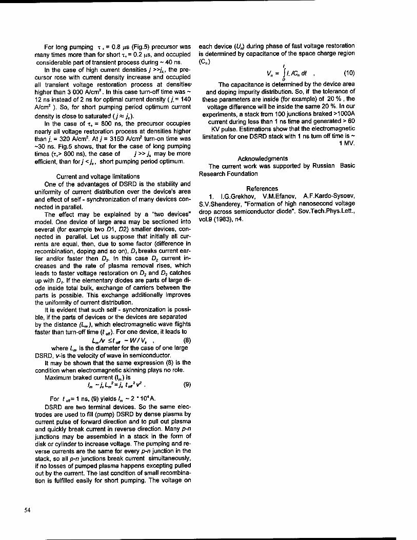
For long pumping x ♦ = 0.8 us (Fig.5) precursor was many times more than for short T+ = 0.2 us, and occupied considerable part of transient process during ~ 40 ns.
In the case of high current densities/ »js, the pre- cursor rose with current density increase and occupied all transient voltage restoration process at densities1
higher than 3 000 A/cm2. In this case turn-off time was ~ 12 ns instead of 2 ns for optimal current density (/.= 140 A/cm2 ). So, for short pumping period optimum current density is close to saturated (/» j,).
In the case of T+ = 800 ns, the precursor occupies nearly all voltage restoration process at densities higher than j. = 320 A/cm2. Aty = 3150 A/cm2 turn-on time was ~30 ns. Fig.5 shows, that for the case of long pumping times (T+> 800 ns), the case of / »j, may be more efficient, than fory <;,, short pumping period optimum.
Current and voltage limitations One of the advantages of DSRD is the stability and
uniformity of current distribution over the device's area and effect of self - synchronization of many devices con- nected in parallel.
The effect may be explained by a "two devices" model. One device of large area may be sectioned into several (for example two D1, D2) smaller devices, con- nected in parallel. Let us suppose that initially all cur- rents are equal, then, due to some factor (difference in recombination, doping and so on), D, breaks current ear- lier and/or faster then D2. In this case D2 current in- creases and the rate of plasma removal rises, which leads to faster voltage restoration on D2 and D2 catches up with D,. If the elementary diodes are parts of large di- ode inside total bulk, exchange of carriers between the parts is possible. This exchange additionally improves the uniformity of current distribution.
It is evident that such self - synchronization is possi- ble, if the parts of devices or the devices are separated by the distance (Lm), which electromagnetic wave flights faster than turn-off time (f off). For one device, it leads to
I^ArSt« -W/V, , (8) where Lm is the diameter for the case of one large
DSRD, v-is the velocity of wave in semiconductor. It may be shown that the same expression (8) is the
condition when electromagnetic skinning plays no role. Maximum braked current (lm) is
/. ~J,Lm2=j, t„W . (9)
For ton- 1 ns, (9) yields /„ - 2 * 104A. DSRD are two terminal devices. So the same elec-
trodes are used to fill (pump) DSRD by dense plasma by current pulse of forward direction and to pull out plasma and quickly break current in reverse direction. Many p-n junctions may be assembled in a stack in the form of disk or cylinder to increase voltage. The pumping and re- verse currents are the same for every p-n junction in the stack, so all p-n junctions break current simultaneously, if no losses of pumped plasma happens excepting pulled out by the current. The last condition of small recombina- tion is fulfilled easily for short pumping. The voltage on
each device (U„) during phase of fast voltage restoration is determined by capacitance of the space charge region (C„) ,
Vn= \i/Cndt , (10) o
The capacitance is determined by the device area and doping impurity distribution. So, if the tolerance of
these parameters are inside (for example) of 20 % , the voltage difference will be inside the same 20 %. In our
experiments, a stack from 100 junctions braked >1000A current during less than 1 ns time and generated > 60 KV pulse. Estimations show that the electromagnetic
limitation for one DSRD stack with 1 ns turn off time is ~ 1 MV.
Acknowledgments The current work was supported by Russian
Research Foundation Basic
References 1. I.G.Grekhov, V.M.Efanov, A.F.Kardo-Sysoev,
S.V.Shenderey, "Formation of high nanosecond voltage drop across semiconductor diode". Sov.Tech.Phys.Lett., vol.9 (1983), n4.
54
Compact Modulator Using Inductive Energy Storage and a Solid State Opening Switch
James C. Dickens, John Bridges and M. Kristiansen Texas Tech University
Pulsed Power Laboratory Department of Electrical Engineering
Lubbock,TX 79409-3102, USA
Abstract
A compact modulator system using inductive energy storage and a diode as an opening switch was investigated. The system was designed around a Russian diode that has characteristics similar to those of a step-recovery diode except that the reverse current density is 10-100 times larger than in U.S. manufactured diodes. The main goal of this investigation was to characterize the Russian diode and develop an understanding of its operation for possible improvement and integration into nanosecond pulse generators. The basic modulator circuit designed uses IGBT's in the forward pumping circuit and is capable of delivering 5 kV at 400 A into the diode. Using this forward pumping circuit, diode voltage and current measurements were made at several input power levels. In addition, data obtained using this test stand was used to produce a computer simulation model of the diode for a more thorough circuit analysis.
Nomenclature
Ic Inductor current.
Vc Capacitor voltage.
Id SOS diode current.
vd SOS diode voltage.
ts SOS diode turn-off time.
tr Reverse pumping time.
tf Forward pumping time.
Introduction
Environmental considerations have made it mandatory to remove various pollutants, such as nitrogen and sulfur oxides (NOX and SOX) from flue gases on fossil fuel power plants. In principle, it is
This work was sponsored by The Texas Tech University Center for Energy Research.
known how to do this (passing the gases through corona discharge regions) but in practice it has been found very difficult to achieve the kind of reliability and energy efficiency that the power industry requires for such systems. A simplified diagram of the removal system is shown in Figure 1. The main problems are the lifetime of the required high voltage repetitive switch (which must be able to operate for over 109
shots) and the electrical efficiency of the overall system.
Pulse input
Outer Conductor
Gas, input
Input
Center Conductor
Corona Discharge Region
Outer Conductor , Stand-offs
Figure 1. Simplified drawing of a SOX and NOX removal system.
Several researchers have found that high ozone production efficiencies (relates closely to the SOX and NOX removal efficiencies) are obtained using short high voltage pulses (pulse length<100 ns and Vp 50- 250 kV) [1,2]. Historically, this type of pulse has been generated by using capacitor or transmission line storage and switched using spark gaps. Recently, a relatively new Russian solid state opening switch technology has been investigate for the production of such pulses. In a pulse generator utilizing this
0-7803-3076-5/96/$5.00 © 1996 IEEE 55
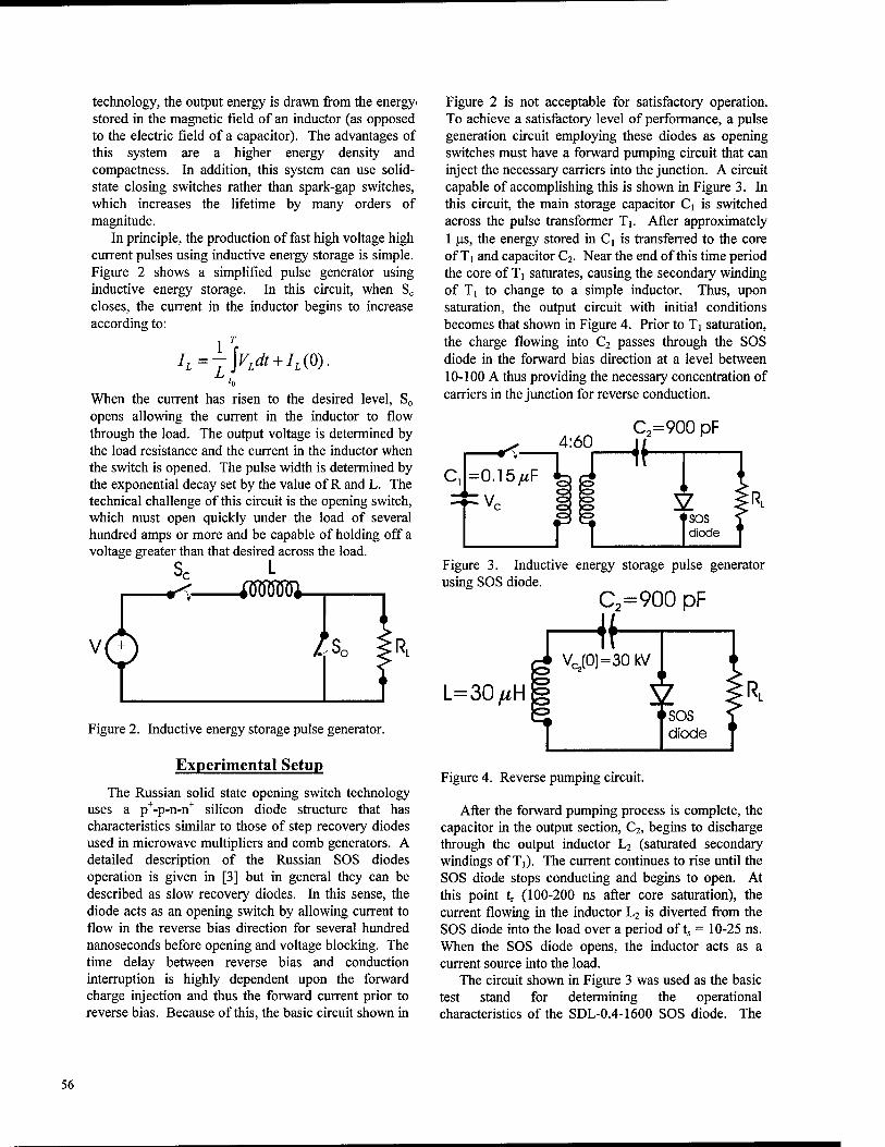
technology, the output energy is drawn from the energy stored in the magnetic field of an inductor (as opposed to the electric field of a capacitor). The advantages of this system are a higher energy density and compactness. In addition, this system can use solid- state closing switches rather than spark-gap switches, which increases the lifetime by many orders of magnitude.
In principle, the production of fast high voltage high current pulses using inductive energy storage is simple. Figure 2 shows a simplified pulse generator using inductive energy storage. In this circuit, when Sc
closes, the current in the inductor begins to increase according to:
T 1 f
+ /L(0)-
When the current has risen to the desired level, S0
opens allowing the current in the inductor to flow through the load. The output voltage is determined by the load resistance and the current in the inductor when the switch is opened. The pulse width is determined by the exponential decay set by the value of R and L. The technical challenge of this circuit is the opening switch, which must open quickly under the load of several hundred amps or more and be capable of holding off a voltage greater than that desired across the load.
L
V 0 A
Figure 2. Inductive energy storage pulse generator.
Experimental Setup
The Russian solid state opening switch technology uses a p+-p-n-n+ silicon diode structure that has characteristics similar to those of step recovery diodes used in microwave multipliers and comb generators. A detailed description of the Russian SOS diodes operation is given in [3] but in general they can be described as slow recovery diodes. In this sense, the diode acts as an opening switch by allowing current to flow in the reverse bias direction for several hundred nanoseconds before opening and voltage blocking. The time delay between reverse bias and conduction interruption is highly dependent upon the forward charge injection and thus the forward current prior to reverse bias. Because of this, the basic circuit shown in
Figure 2 is not acceptable for satisfactory operation. To achieve a satisfactory level of performance, a pulse generation circuit employing these diodes as opening switches must have a forward pumping circuit that can inject the necessary carriers into the junction. A circuit capable of accomplishing this is shown in Figure 3. In this circuit, the main storage capacitor Q is switched across the pulse transformer Ti. After approximately 1 us, the energy stored in Ci is transferred to the core of Ti and capacitor C2. Near the end of this time period the core of Ti saturates, causing the secondary winding of Ti to change to a simple inductor. Thus, upon saturation, the output circuit with initial conditions becomes that shown in Figure 4. Prior to Ti saturation, the charge flowing into C2 passes through the SOS diode in the forward bias direction at a level between 10-100 A thus providing the necessary concentration of carriers in the junction for reverse conduction.
=0,15MF L
4:60 C2=900 pF
Vr
Figure 3. Inductive energy storage pulse generator using SOS diode.
C2=900 pF
tt
L=30/*H
VC2(0)=30kV
s RL SOS diode
Figure 4. Reverse pumping circuit.
After the forward pumping process is complete, the capacitor in the output section, C2, begins to discharge through the output inductor L2 (saturated secondary windings of Tj). The current continues to rise until the SOS diode stops conducting and begins to open. At this point t, (100-200 ns after core saturation), the current flowing in the inductor L2 is diverted from the SOS diode into the load over a period of ts = 10-25 ns. When the SOS diode opens, the inductor acts as a current source into the load.
The circuit shown in Figure 3 was used as the basic test stand for determining the operational characteristics of the SDL-0.4-1600 SOS diode. The
56
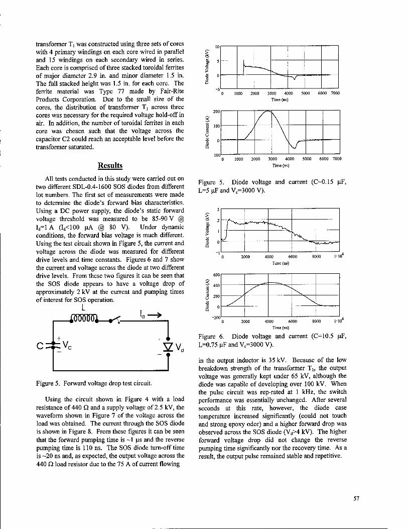
transformer Ti was constructed using three sets of cores with 4 primary windings on each core wired in parallel and 15 windings on each secondary wired in series. Each core is comprised of three stacked toroidal ferrites of major diameter 2.9 in. and minor diameter 1.5 in. The full stacked height was 1.5 in. for each core. The ferrite material was Type 77 made by Fair-Rite Products Corporation. Due to the small size of the cores, the distribution of transformer T] across three cores was necessary for the required voltage hold-off in air. In addition, the number of toroidal ferrites in each core was chosen such that the voltage across the capacitor C2 could reach an acceptable level before the transformer saturated.
Results
All tests conducted in this study were carried out on two different SDL-0.4-1600 SOS diodes from different lot numbers. The first set of measurements were made to determine the diode's forward bias characteristics. Using a DC power supply, the diode's static forward voltage threshold was measured to be 85-90 V @ Id=lA (Id<100 uA @ 80 V). Under dynamic conditions, the forward bias voltage is much different. Using the test circuit shown in Figure 5, the current and voltage across the diode was measured for different drive levels and time constants. Figures 6 and 7 show the current and voltage across the diode at two different drive levels. From these two figures it can be seen that the SOS diode appears to have a voltage drop of approximately 2 kV at the current and pumping times of interest for SOS operation.
Vr
Figure 5. Forward voltage drop test circuit.
Using the circuit shown in Figure 4 with a load resistance of 440 Q and a supply voltage of 2.5 kV, the waveform shown in Figure 7 of the voltage across the load was obtained. The current through the SOS diode is shown in Figure 8. From these figures it can be seen that the forward pumping time is ~1 us and the reverse pumping time is 110 ns. The SOS diode turn-off time is -20 ns and, as expected, the output voltage across the 440 Q load resistor due to the 75 A of current flowing
10
I ao 5
0 1000 2000 3000 4000 5000 6000 7000
Time (ns)
200
<
1 100
u
I o 5
-100 0 1000 2000 3000 4000 5000 6000 7000
Time (ns)
Figure 5. Diode voltage and current (C=0.15 uF, L=5 uF and Vc=3000 V).
? &
3
1
1
0
4000 6000 Time (ns)
1-10
600
4UU
20U
0
0 2000 4000 6000 8000 1'10
Time (ns)
Figure 6. Diode voltage and current (C=10.5 uF, L=0.75 uF and Vc=3000 V).
in the output inductor is 35 kV. Because of the low breakdown strength of the transformer T1; the output voltage was generally kept under 65 kV, although the diode was capable of developing over 100 kV. When the pulse circuit was rep-rated at 1 kHz, the switch performance was essentially unchanged. After several seconds at this rate, however, the diode case temperature increased significantly (could not touch and strong epoxy odor) and a higher forward drop was observed across the SOS diode (Vd>4 kV). The higher forward voltage drop did not change the reverse pumping time significantly nor the recovery time. As a result, the output pulse remained stable and repetitive.
57
10
>
I ~10 >
f O
-20
-30
-40
r "~-v. ■ y
I 500 2000 2500 3000 1000 1500
Time (ns)
Figure 7. Pulser output voltage across a 440 Q resistor (Vcl=2500 V).
2500 3000
5
-100 1000 1500
Time (ns)
Figure 8. SOS diode current (Vc,=2500 V).
Discussion
From Figure 8 it can be seen that the current in the output inductor (secondary winding of Ti after saturation) fails to reach its maximum level before the SOS diode stops conducting. From the circuit parameters, the ■/« wave period of the reverse pumping circuit was calculated to be 250 ns, considerably longer than the 110 ns reverse conduction time of the SOS diode. Because of this, the energy transfer efficiency is less than 40% (based upon the energy stored in Ct to energy delivered to the load). The main reason for the long reverse time period is the large number of turns required on the secondary winding of T|. The use of larger cores would increase the coupling coefficient and reduce the leakage inductance of T\. This in turn would reduce the number of turns required on the secondary while still maintaining the simplicity of the circuit. Due to the large lead time in manufacturing large custom ferrite toroids, tests with the improved transformer design have not been completed. For even better performance at the cost of complexity, intermediate pulse compression stages or additional magnetic switches can be placed in the circuit [4,5].
The main limitation on the use of SOS diodes in repetitive nanosecond pulse generators is their high thermal resistance. All other components in the pulse generation circuit showed little observable heating during the 1 kHz rep-rate test. The SOS diode, however, far exceeded an acceptable temperature rise within 60 sec. Although oil can be used to help reduce the heat rise, better thermal management techniques must be employed in the diode for long duration high rep-rate operation.
References
1. S. Masuda, M. Sato, and T. Seki, "High-Efficiency Ozonizer Using Traveling Wave Pulse Voltage, " IEEE Transactions on Industry Applications, Vol. IA-22 No., 5, September/October, 1986.
2. J. Salge, H. Karner, M. Labrenz, K. Scheibe, and P. Braumann, "Characteristics of Ozonizers Supplied by Fast Rising Voltage," Proceedings of the 6' International Conference On Gas Discharge and their Applications, Edinburgh, Scotland, Sept. 8-11, 1980.
3. G. A. Mesyats, S. N. Rukin, S. K. Lyubutin, et al. "Semiconductor opening switch research at IEP," Proceedings of the 10''' IEEE International Pulsed Power Conference, Albuquerque, NM, 1995.
4. G. A. Mesyats, S. N. Rukin, S. K. Lyubutin, et al. "Megavolt nanosecond 50kW average power all-solid state driver for commercial applications," Proceedings of the 10"' IEEE International Pulsed Power Conference, Albuquerque, NM, 1995.
5. S. N. Rukin, S. K. Lyubutin, V. V. Kostirev, V. A. Telnov, "Repetitive 200 kV nanosecond all-solid-state pulser with a semiconductor opening switch," Proceedings of the I0'h IEEE International Pulsed Power Conference, Albuquerque, NM, 1995.
58
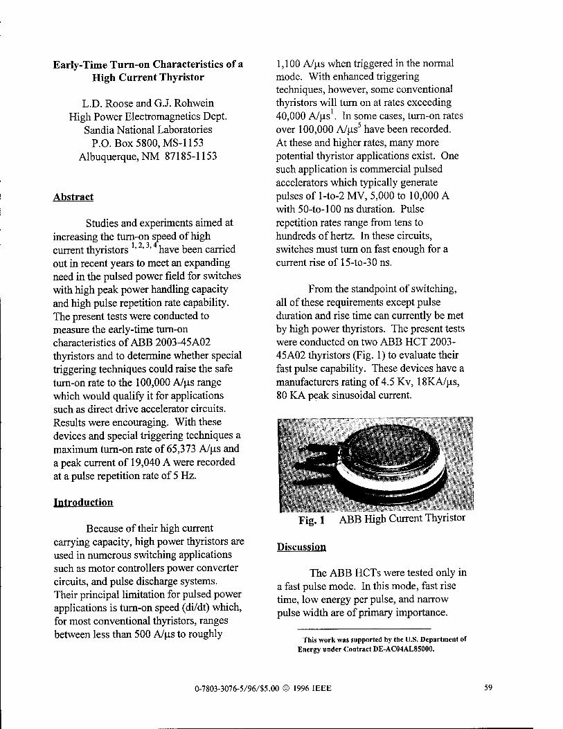
Early-Time Turn-on Characteristics of a High Current Thyristor
L.D. Roose and G.J. Rohwein High Power Electromagnetics Dept.
Sandia National Laboratories P.O. Box 5800, MS-1153
Albuquerque, NM 87185-1153
Abstract
Studies and experiments aimed at increasing the turn-on speed of high current thyristors l'2'3'4 have been carried out in recent years to meet an expanding need in the pulsed power field for switches with high peak power handling capacity and high pulse repetition rate capability. The present tests were conducted to measure the early-time turn-on characteristics of ABB 2003-45 A02 thyristors and to determine whether special triggering techniques could raise the safe turn-on rate to the 100,000 A/us range which would qualify it for applications such as direct drive accelerator circuits. Results were encouraging. With these devices and special triggering techniques a maximum turn-on rate of 65,373 A/us and a peak current of 19,040 A were recorded at a pulse repetition rate of 5 Hz.
Introduction
Because of their high current carrying capacity, high power thyristors are used in numerous switching applications such as motor controllers power converter circuits, and pulse discharge systems. Their principal limitation for pulsed power applications is turn-on speed (di/dt) which, for most conventional thyristors, ranges between less than 500 A/us to roughly
1,100 A/us when triggered in the normal mode. With enhanced triggering techniques, however, some conventional thyristors will turn on at rates exceeding 40,000 A/us1. In some cases, turn-on rates over 100,000 A/us5 have been recorded. At these and higher rates, many more potential thyristor applications exist. One such application is commercial pulsed accelerators which typically generate pulses of l-to-2 MV, 5,000 to 10,000 A with 50-to-100 ns duration. Pulse repetition rates range from tens to hundreds of hertz. In these circuits, switches must turn on fast enough for a current rise of 15-to-30 ns.
From the standpoint of switching, all of these requirements except pulse duration and rise time can currently be met by high power thyristors. The present tests were conducted on two ABB HCT 2003- 45A02 thyristors (Fig. 1) to evaluate their fast pulse capability. These devices have a manufacturers rating of 4.5 Kv, 18KA/us, 80 KA peak sinusoidal current.
:' "■
Fig. 1 ABB High Current Thyristor
Discussion
The ABB HCTs were tested only in a fast pulse mode. In this mode, fast rise time, low energy per pulse, and narrow pulse width are of primary importance.
This work was supported by the U.S. Department of Energy under Contract DE-AC04AL85000.
0-7803-3076-5/96/S5.00 © 1996 IEEE 59
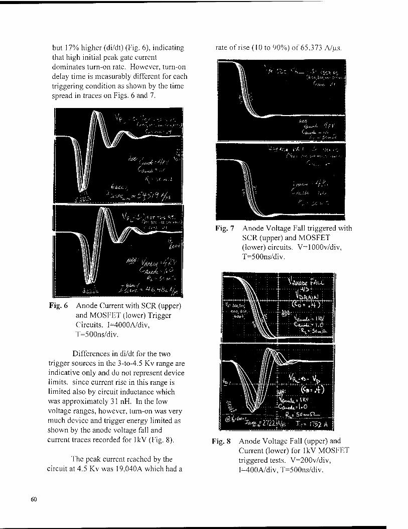
but 17% higher (di/dt) (Fig. 6), indicating that high initial peak gate current dominates turn-on rate. However, turn-on delay time is measurably different for each triggering condition as shown by the time spread in traces on Figs. 6 and 7.
rate of rise (10 to 90%) of 65,373 A/us.
y/}A.c/j£ -y/
Fig. 6 Anode Current with SCR (upper) and MOSFET (lower) Trigger Circuits. I=4000A/div, T=500ns/div.
Differences in di/dt for the two trigger sources in the 3-to-4.5 Kv range are indicative only and do not represent device limits, since current rise in this range is limited also by circuit inductance which was approximately 31 nH. In the low voltage ranges, however, turn-on was very much device and trigger energy limited as shown by the anode voltage fall and current traces recorded for lkV (Fig. 8).
The peak current reached by the circuit at 4.5 Kv was 19,040A which had a
Fig. 7 Anode Voltage Fall triggered with SCR (upper) and MOSFET (lower) circuits. V=1000v/div, T=500ns/div.
ii-T-if^t-i i K&T&JT
;RLv5o.«A-
-:--i-..Rv?'5,,vrilr_
Fig. 8 Anode Voltage Fall (upper) and Current (lower) for lkV MOSFET triggered tests. V=200v/div, I=400A/div, T=500ns/div.
60
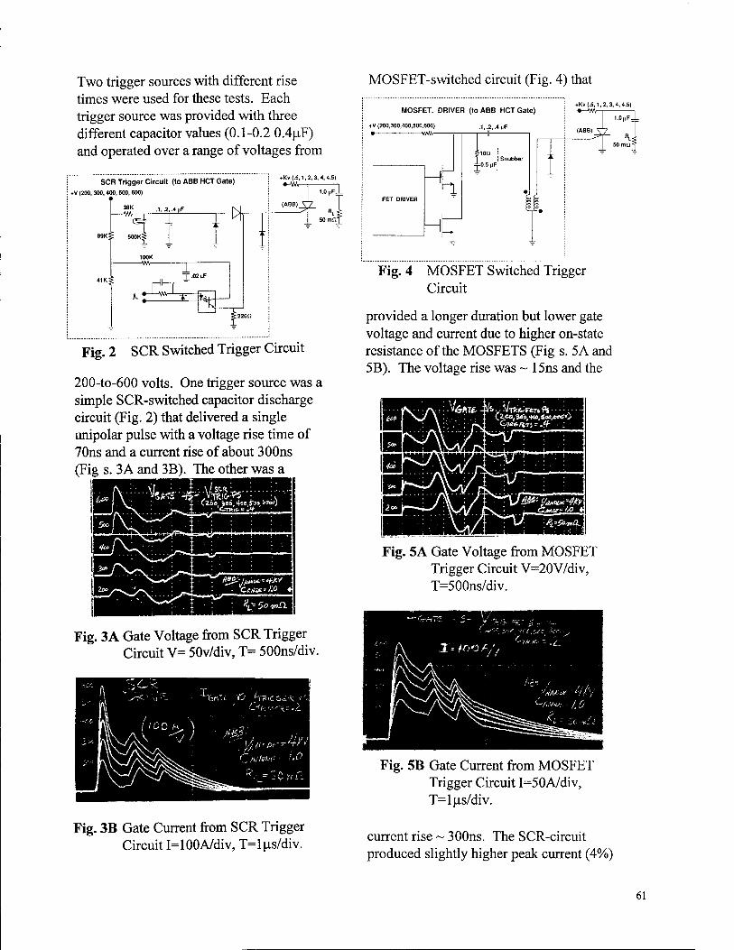
Two trigger sources with different rise times were used for these tests. Each trigger source was provided with three different capacitor values (0.1-0.2 0.4uF) and operated over a range of voltages from
SCR Trigger Circuit (to ABB HCT Gate) i »V (200, 300,400, 500, 600)
+Kv(.5,1,2, 3, 4, 4.5) •-VW—i 1
i—^K , -i-y*
89KS 5O0K? I I ^
100K
«-L-Wr-Ljr
I X-02|lF
fel fc
Fig. 2 SCR Switched Trigger Circuit
200-to-600 volts. One trigger source was a simple SCR-switched capacitor discharge circuit (Fig. 2) that delivered a single unipolar pulse with a voltage rise time of 70ns and a current rise of about 300ns (Fig s. 3A and 3B). The other was a
Fig. 3A Gate Voltage from SCR Trigger Circuit V= 50v/div, T= 500ns/div.
Fig. 3B Gate Current from SCR Trigger Circuit I=100A/div, T=l|is/div.
MOSFET-switched circuit (Fig. 4) that
MOSFET. DRIVER (to ABB HCT Gate)
♦V (200,300,400,500,600) .1, .2, .4 uF • WfA
n £10:
n'
HL
*Kv(.5,1,2, 3, 4, 4.5) »-Wr-r- 1
I.O^FJ
(ABB) vV
50 mQ5
Fig. 4 MOSFET Switched Trigger Circuit
provided a longer duration but lower gate voltage and current due to higher on-state resistance of the MOSFETS (Fig s. 5 A and 5B). The voltage rise was ~ 15ns and the
-.:..'::■ C?.0C|3«'»,«<',*<».««:v
Fig. 5A Gate Voltage from MOSFET Trigger Circuit V=20V/div, T=500ns/div.
Fig. 5B Gate Current from MOSFET Trigger Circuit I=50A/div, T=lus/div.
current rise ~ 300ns. The SCR-circuit produced slightly higher peak current (4%)
61
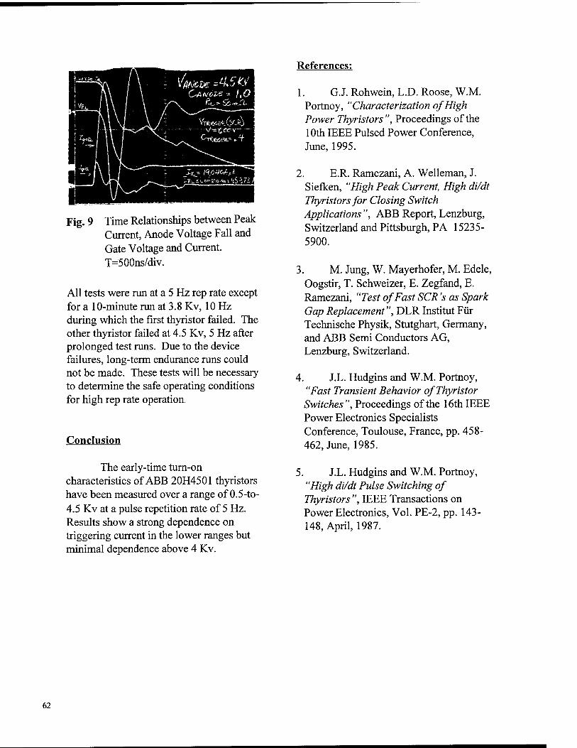
Fig. 9 Time Relationships between Peak Current, Anode Voltage Fall and Gate Voltage and Current. T=500ns/div.
All tests were run at a 5 Hz rep rate except for a 10-minute run at 3.8 Kv, 10 Hz during which the first thyristor failed. The other thyristor failed at 4.5 Kv, 5 Hz after prolonged test runs. Due to the device failures, long-term endurance runs could not be made. These tests will be necessary to determine the safe operating conditions for high rep rate operation.
Conclusion
The early-time turn-on characteristics of ABB 20H4501 thyristors have been measured over a range of 0.5-to- 4.5 Kv at a pulse repetition rate of 5 Hz. Results show a strong dependence on triggering current in the lower ranges but minimal dependence above 4 Kv.
References:
1. G. J. Rohwein, L.D. Roose, W.M. Portnoy, "Characterization of High Power Thyristors", Proceedings of the 10th IEEE Pulsed Power Conference, June, 1995.
2. E.R. Ramezani, A. Welleman, J. Siefken, "High Peak Current, High di/dt Thyristors for Closing Switch Applications ", ABB Report, Lenzburg, Switzerland and Pittsburgh, PA 15235- 5900.
3. M. Jung, W. Mayerhofer, M. Edele, Oogstir, T. Schweizer, E. Zegfand, E. Ramezani, "Test of Fast SCR's as Spark Gap Replacement", DLR Institut Für Technische Physik, Stutghart, Germany, and ABB Semi Conductors AG, Lenzburg, Switzerland.
4. J.L. Hudgins and W.M. Portnoy, "Fast Transient Behavior of Thyristor Switches", Proceedings of the 16th IEEE Power Electronics Specialists Conference, Toulouse, France, pp. 458- 462, June, 1985.
5. J.L. Hudgins and W.M. Portnoy, "High di/dt Pulse Switching of Thyristors ", IEEE Transactions on Power Electronics, Vol. PE-2, pp. 143- 148, April, 1987.
62

All-Solid-State Exciter for High-Power, High-Repetition-Rate Excimer Laser
F.Endo, K. Okamura, K. Kakizaki, S. Takagi, E. Kaneko
TOSHIBA Corporation, 1 Toshiba-cho, Fuchu-shi, Tokyo 183, Japan
Abstract
An all-solid-state exciter has been developed for a high-power, high-repetition-rate XeCl excimer laser. It is composed of a semiconductor switch using MAGTs (MOS Assisted Gate-Triggered Thyristors) and a single-stage Magnetic Pulse Compression circuit (MPC). The semiconductor switch, comprising thirty-two series and two parallel MAGTs, generated a 25 kV - 2 kA - 0.8 u.s pulse, which was compressed to a 200 ns pulse by the MPC.
Continuous operation with an average laser power of 260 W at a repetition rate of 2 kHz was verified by applying the exciter to a XeCl excimer laser. A switch efficiency of 77% was achieved at 2 kHz operation for a switching energy of 11.3 J. Furthermore, 440 mJ - 220 W at 500 Hz was obtained by increasing the switching energy (= 33.8 J) and discharge volume. Experimental results verified that this all-solid-state exciter can replace thyratrons.
Introduction
In designing high-power, high-repetition-rate excimer laser system for industrial applications such as semiconductor and material processing, it is important to minimize their running costs, and especially their maintenance costs. One way of achieving this is to adopt an all-solid-state exciter to provide a long service life. Development of an all-solid-state exciter for such a laser have already been reported.1'1 Its exciter has a complicated scheme, however, because it is composed of two parallel thyristor switches, each with a pulse transformer, and four- stage series Magnetic Pulse Compression circuits (MPCs).
We developed a simple and high-efficiency all-solid- state exciter composed of a semiconductor switch using newly developed devices, MAGTs (MOS Assisted Gate- Triggered Thyristors), and a single-stage MPC.[2I[3]
However, it can drive excimer lasers of only a few tens of watts.
This paper describes the design of an all-solid-state exciter which can drive a XeCl excimer laser of several hundred watts and experimental results of high-power, high- repetition-rate XeCl laser operation using this exciter.
AU-solid-state exciter
Design concept
Exciter requirements are an output voltage of 20kV and a voltage rise time of 200 ns for an efficient pumping of a 2 kHz - 200 W XeCl excimer laser which has a discharge volume of 1 (W) x 2.4 (H) x 70 (L) cm3 and a gas mixture of
Xe/HCl/Ne=2/0.27/278 kPa. Figure 1 shows a schematic diagram of our all-solid-state exciter. The switch generated a 25 kV - 2 kA - 0.8 u.s pulse and the MPC compressed its pulse width into 200 ns. The specifications of the semiconductor switch and the MPC are summarized in Table 1 and Table 2, respectively.
25kV
Semiconductor switch MPC
Fig. 1. Schematic diagram of the all-solid-state exciter.
Table 1 Specifications of the semiconductor switch.
Items spec. Voltage 25 kV Current 2kA
Pulse width 0.8us Repetition rate 2 kHz
Table 2 Specifications of the MPC.
Items spec. Operating voltage 22 kV Time to saturation 0.8ns Compression ratio 4
Semiconductor switch
MAGT: The MAGT, which is a kind of MOS-driven thyristors, was especially designed for high-repetition-rate pulsed power supplies.[4'[5] It provides the advantages of both the high power handling capability of thyristors and the
0-7803-3076-5/96/S5.00 © 1996 IEEE 63
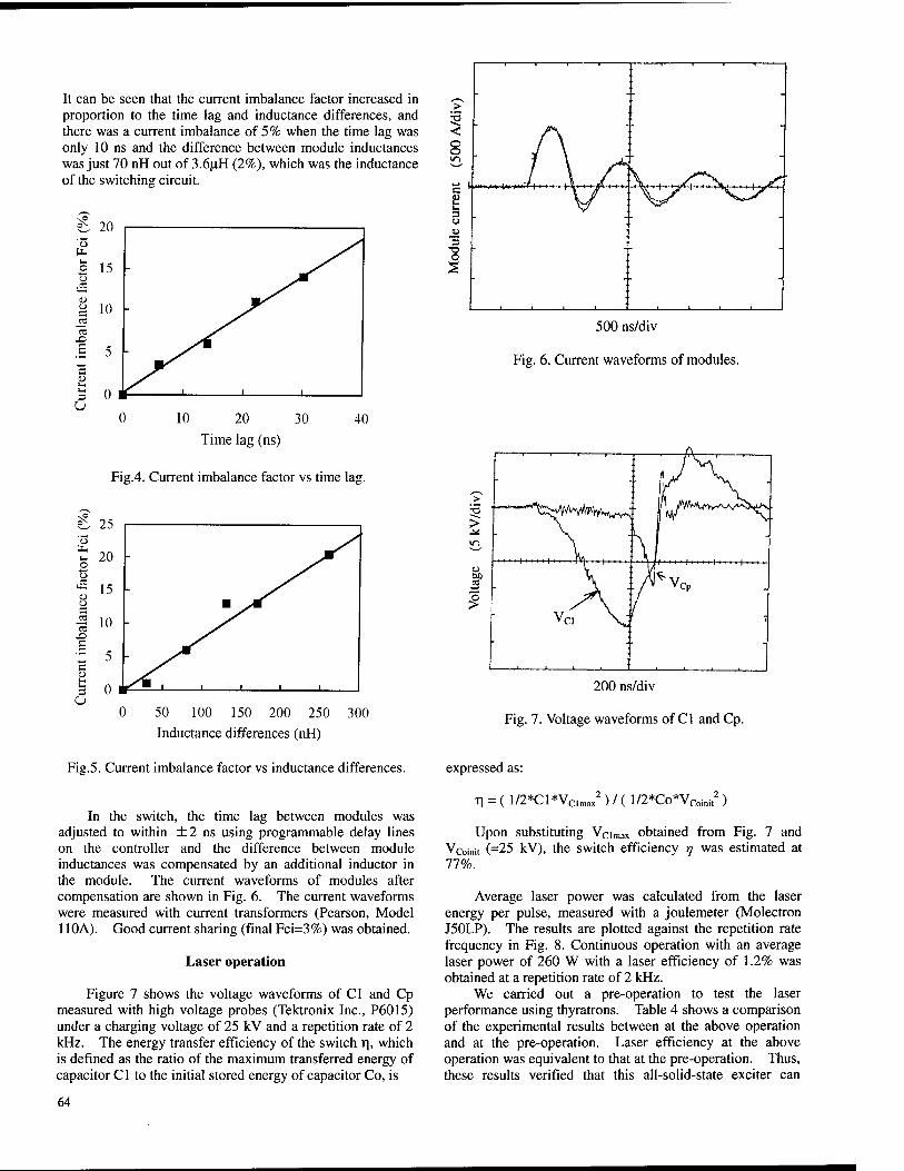
It can be seen that the current imbalance factor increased in proportion to the time lag and inductance differences, and there was a current imbalance of 5% when the time lag was only 10 ns and the difference between module inductances was just 70 nH out of 3.6uH (2%), which was the inductance of the switching circuit.
10 20 30
Time lag (ns)
40
Fig.4. Current imbalance factor vs time lag.
50 100 150 200 250
Inductance differences (nH) 300
Fig.5. Current imbalance factor vs inductance differences.
In the switch, the time lag between modules was adjusted to within +2 ns using programmable delay lines on the controller and the difference between module inductances was compensated by an additional inductor in the module. The current waveforms of modules after compensation are shown in Fig. 6. The current waveforms were measured with current transformers (Pearson, Model 110A). Good current sharing (final Fci=3%) was obtained.
Laser operation
Figure 7 shows the voltage waveforms of Cl and Cp measured with high voltage probes (Tektronix Inc., P6015) under a charging voltage of 25 kV and a repetition rate of 2 kHz. The energy transfer efficiency of the switch T|, which is defined as the ratio of the maximum transferred energy of capacitor Cl to the initial stored energy of capacitor Co, is
500 ns/div
Fig. 6. Current waveforms of modules.
200 ns/div
Fig. 7. Voltage waveforms of Cl and Cp.
expressed as:
Ti = ( l/2*Cl*Vclmax2) / ( l/2*Co*Vc„i„it2)
Upon substituting VCimax obtained from Fig. 7 and Vcoinit (=25 kV), the switch efficiency r/ was estimated at 77%.
Average laser power was calculated from the laser energy per pulse, measured with a joulemeter (Molectron J50LP). The results are plotted against the repetition rate frequency in Fig. 8. Continuous operation with an average laser power of 260 W with a laser efficiency of 1.2% was obtained at a repetition rate of 2 kHz.
We carried out a pre-operation to test the laser performance using thyratrons. Table 4 shows a comparison of the experimental results between at the above operation and at trie pre-operation. Laser efficiency at the above operation was equivalent to that at the pre-operation. Thus, these results verified that this all-solid-state exciter can
64
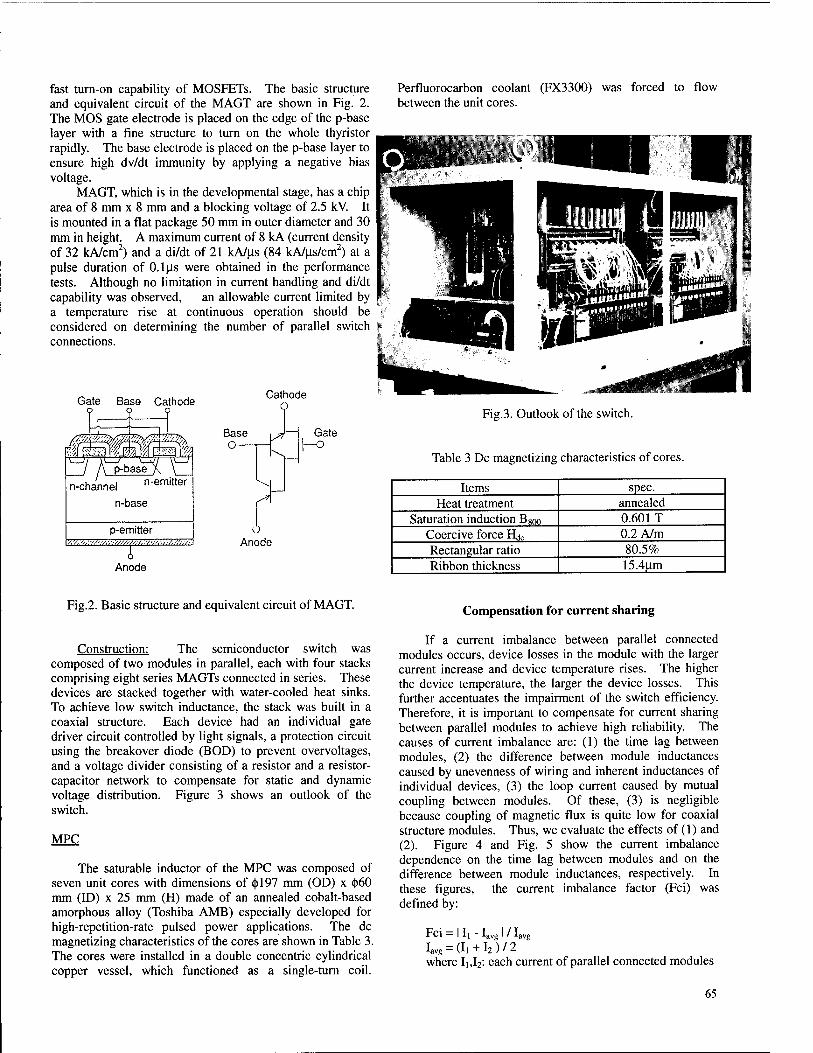
fast turn-on capability of MOSFETs. The basic structure and equivalent circuit of the MAGT are shown in Fig. 2. The MOS gate electrode is placed on the edge of the p-base layer with a fine structure to turn on the whole thyristor rapidly. The base electrode is placed on the p-base layer to ensure high dv/dt immunity by applying a negative bias voltage.
MAGT, which is in the developmental stage, has a chip area of 8 mm x 8 mm and a blocking voltage of 2.5 kV. It is mounted in a flat package 50 mm in outer diameter and 30 mm in height. A maximum current of 8 kA (current density of 32 kA/cm2) and a di/dt of 21 kA/ps (84 kA/ps/cm2) at a pulse duration of 0.1 ps were obtained in the performance tests. Although no limitation in current handling and di/dt capability was observed, an allowable current limited by a temperature rise at continuous operation should be considered on determining the number of parallel switch connections.
Gate Base Cathode o
Cathode o
n-channel n-emitter
n-base
p-emitter
Anode
Base o—
<
>■
Gate l-o
o Anode
Perfluorocarbon coolant between the unit cores.
(FX3300) was forced to flow
Fig.3. Outlook of the switch.
Table 3 Dc magnetizing characteristics of cores.
Items spec. Heat treatment annealed
Saturation induction B8oo 0.601 T Coercive force Hdc 0.2 A/m Rectangular ratio 80.5% Ribbon thickness 15.4pm
Fig.2. Basic structure and equivalent circuit of MAGT. Compensation for current sharing
Construction: The semiconductor switch was composed of two modules in parallel, each with four stacks comprising eight series MAGTs connected in series. These devices are stacked together with water-cooled heat sinks. To achieve low switch inductance, the stack was built in a coaxial structure. Each device had an individual gate driver circuit controlled by light signals, a protection circuit using the breakover diode (BOD) to prevent overvoltages, and a voltage divider consisting of a resistor and a resistor- capacitor network to compensate for static and dynamic voltage distribution. Figure 3 shows an outlook of the switch.
MPC
The saturable inductor of the MPC was composed of seven unit cores with dimensions of <pl97 mm (OD) x <|>60 mm (ID) x 25 mm (H) made of an annealed cobalt-based amorphous alloy (Toshiba AMB) especially developed for high-repetition-rate pulsed power applications. The dc magnetizing characteristics of the cores are shown in Table 3. The cores were installed in a double concentric cylindrical copper vessel, which functioned as a single-turn coil.
If a current imbalance between parallel connected modules occurs, device losses in the module with the larger current increase and device temperature rises. The higher the device temperature, the larger the device losses. This further accentuates the impairment of the switch efficiency. Therefore, it is important to compensate for current sharing between parallel modules to achieve high reliability. The causes of current imbalance are: (1) the time lag between modules, (2) the difference between module inductances caused by unevenness of wiring and inherent inductances of individual devices, (3) the loop current caused by mutual coupling between modules. Of these, (3) is negligible because coupling of magnetic flux is quite low for coaxial structure modules. Thus, we evaluate the effects of (1) and (2). Figure 4 and Fig. 5 show the current imbalance dependence on the time lag between modules and on the difference between module inductances, respectively. In these figures, the current imbalance factor (Fci) was defined by:
Fci I.
■ Iavg I / laVg Hi avg-dl+l2)/2
where Ii,I2: each current of parallel connected modules
65
replace thyratrons.
Table 4 Comparison of the results between at this operation and at the pre-operation at repetition rate of 2 kHz.
Items This operation Pre-operation
Power supply All-solid-state exciter
Two thyratrons
Co/Cl/Cp 36/36/32 nF 32/32/32 nF
Charging voltage 25 kV 19 kV Charging energy 11.3 J 5.8 J
Laser energy 130 mJ 73 mJ Laser efficiency 1.2% 1.3%
We also tried higher laser energy operation (high energy mode). Operating conditions are shown in Table 5 in comparison with the conditions of the former operation (high-rep-rate mode).
Conclusion
An all-solid-state exciter composed of a semiconductor switch using a MAGT (MOS Assisted Gate-Triggered Thyristor), and a single-stage Magnetic Pulse Compression circuit (MPC) was developed for a high-power, high- repetition-rate XeCl excimer laser. By applying this exciter to a 2 kHz - 200 W XeCl excimer laser, an average laser power of 260 W was attained at a repetition rate of 2 kHz. The resulting switch efficiency and laser efficiency were 77% and 1.2%, respectively. Furthermore, 440 mJ - 220 W at 500 Hz was obtained by increasing the switching energy and discharge volume. The experimental results verified that the all-solid-state exciter can replace thyratrons.
This work was conducted as a joint research project with the New Energy and Industrial Technology Development Organization of Japan.
References
Table 5. Operating conditions.
Items High energy mode High-rep-rate mode Repetition rate 500 Hz 2000 Hz
Charging energy 33.8 J 11.3 J Co/Cl/Cp 108/108/108 nF 36/36/32 nF
Discharge volume 1.8wx2.6Hx70'cm3 lwx2.4Hx70Lcm3
Gas mixture of Xe/HCl/Ne
4/0.4/278 kPa 2/0.27/278 kPa
The average laser power is compared with the results of high-rep-rate mode in Fig. 8. An average laser power of 220 W and a laser energy per pulse of 440 mJ were obtained at a repetition rate of 500 Hz. Laser efficiency was 1%. The maximum laser energy per pulse of 510 mJ was obtained on a single shot basis.
[1] H. M. von Bergmann, et al.:" All-solid-state switched, high repetition rate excimer and C02 TEA laser ", CLEO'91,p.244, 1991
[2] F. Endo, et al.:" Development of semiconductor switch for pulsed power utilizing MAGTs ", 9th Pulsed Power Conference, p.650, 1993
[3] T. Teranishi, et al.:" High repetition rate operation of a magnetic pulse compression circuit for excimer laser ", 9* Pulsed Power Conference, p.791 , 1993
[4] T. Shinohe, et al.: " Design criteria for high frequency, ultra high di/dt MAGTs ", IEDM Tech. Dig., p.153, 1991
[5] F. Endo, et al.: " Pulse switching characteristics of MAGTs for pulsed power applications ", Trans. IEEJ, Vol.114, No.5,p.l08, 1994
300
250
200
2 CL>
3
1.8(W)x2.6(H)x70(L)cm3
,Xe/HCl/Ne=4/0.4/278 kPa
l(W)x2.4(H)x70(L)cni Xe/HCl/Ne=2/0.27/278 kPa
0.5 1 1.5 2 Repetition rate (kHz)
2.5
Fig. 8. Average laser power vs repetition rate.
66
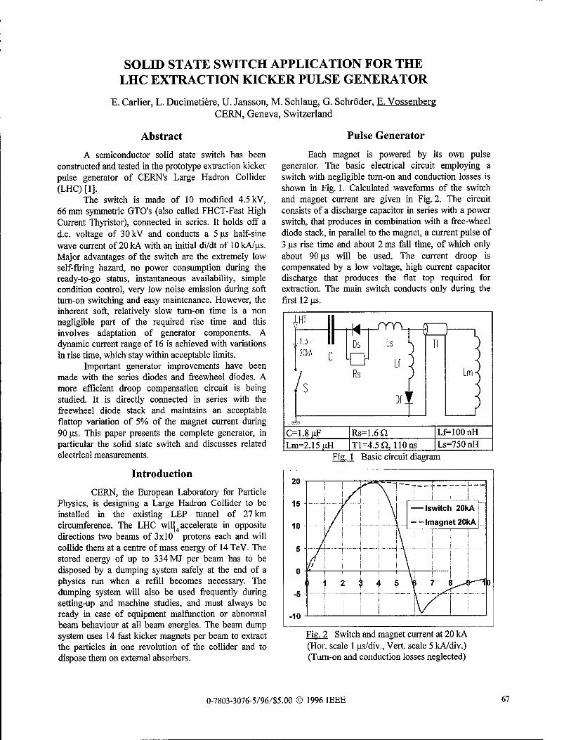
SOLID STATE SWITCH APPLICATION FOR THE LHC EXTRACTION KICKER PULSE GENERATOR
E. Carlier, L. Ducimetiere, U. Jansson, M. Schlaug, G. Schröder, E. Vossenberg CERN, Geneva, Switzerland
Abstract A semiconductor solid state switch has been
constructed and tested in the prototype extraction kicker pulse generator of CERN's Large Hadron Collider (LHC) [1].
The switch is made of 10 modified 4.5 kV, 66 mm symmetric GTO's (also called FHCT-Fast High Current Thyristor), connected in series. It holds off a d.c. voltage of 30 kV and conducts a 5 us half-sine wave current of 20 kA with an initial di/dt of 10 kA/us. Major advantages of the switch are the extremely low self-firing hazard, no power consumption during the ready-to-go status, instantaneous availability, simple condition control, very low noise emission during soft turn-on switching and easy maintenance. However, the inherent soft, relatively slow turn-on time is a non negligible part of the required rise time and this involves adaptation of generator components. A dynamic current range of 16 is achieved with variations in rise time, which stay within acceptable limits.
Important generator improvements have been made with the series diodes and freewheel diodes. A more efficient droop compensation circuit is being studied. It is directly connected in series with the freewheel diode stack and maintains an acceptable flattop variation of 5% of the magnet current during 90 us. This paper presents the complete generator, in particular the solid state switch and discusses related electrical measurements.
Introduction CERN, the European Laboratory for Particle
Physics, is designing a Large Hadron Collider to be installed in the existing LEP tunnel of 27 km circumference. The LHC wil|4 accelerate in opposite directions two beams of 3x10 protons each and will collide them at a centre of mass energy of 14 TeV. The stored energy of up to 334 MJ per beam has to be disposed by a dumping system safely at the end of a physics run when a refill becomes necessary. The dumping system will also be used frequently during setting-up and machine studies, and must always be ready in case of equipment malfunction or abnormal beam behaviour at all beam energies. The beam dump system uses 14 fast kicker magnets per beam to extract the particles in one revolution of the collider and to dispose them on external absorbers.
Pulse Generator
Each magnet is powered by its own pulse generator. The basic electrical circuit employing a switch with negligible turn-on and conduction losses is shown in Fig. 1. Calculated waveforms of the switch and magnet current are given in Fig. 2. The circuit consists of a discharge capacitor in series with a power switch, that produces in combination with a free-wheel diode stack, in parallel to the magnet, a current pulse of 3 us rise time and about 2 ms fall time, of which only about 90 us will be used. The current droop is compensated by a low voltage, high current capacitor discharge that produces the flat top required for extraction. The main switch conducts only during the first 12 us.
C=1.8uF Lm=2.15 nH
Rs=1.6Q T1=4.5Q, 110 ns
LrMOOnH Ls=750nH
Fig. 1 Basic circuit diagram
Fig. 2 Switch and magnet current at 20 kA (Hor. scale 1 us/div., Vert, scale 5 kA/div.) (Turn-on and conduction losses neglected)
O-7803-3076-5/96/S5.OO © 1996 IEEE 67
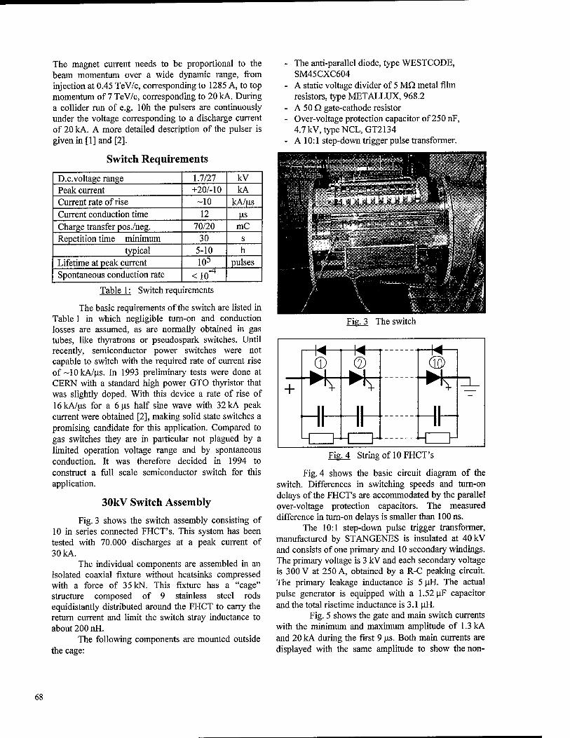
The magnet current needs to be proportional to the beam momentum over a wide dynamic range, from injection at 0.45 TeV/c, corresponding to 1285 A, to top momentum of 7 TeV/c, corresponding to 20 kA. During a collider run of e.g. 10h the pulsers are continuously under the voltage corresponding to a discharge current of 20 kA. A more detailed description of the pulser is given in [1] and [2].
Switch Requirements
D.c.voltage range 1.7/27 kV Peak current +20/-10 kA Current rate of rise -10 kA/us Current conduction time 12 us Charge transfer pos./neg. 70/20 mC Repetition time minimum 30 s
typical 5-10 h Lifetime at peak current 105 pulses Spontaneous conduction rate <i<T
Table 1: Switch requirements
The basic requirements of the switch are listed in Table 1 in which negligible turn-on and conduction losses are assumed, as are normally obtained in gas tubes, like thyratrons or pseudospark switches. Until recently, semiconductor power switches were not capable to switch with the required rate of current rise of -10 kA/us. In 1993 preliminary tests were done at CERN with a standard high power GTO thyristor that was slightly doped. With this device a rate of rise of 16 kA/us for a 6 us half sine wave with 32 kA peak current were obtained [2], making solid state switches a promising candidate for this application. Compared to gas switches they are in particular not plagued by a limited operation voltage range and by spontaneous conduction. It was therefore decided in 1994 to construct a full scale semiconductor switch for this application.
30kV Switch Assembly
Fig. 3 shows the switch assembly consisting of 10 in series connected FHCT's. This system has been tested with 70.000 discharges at a peak current of 30 kA.
The individual components are assembled in an isolated coaxial fixture without heatsinks compressed with a force of 35 kN. This fixture has a "cage" structure composed of 9 stainless steel rods equidistantly distributed around the FHCT to carry the return current and limit the switch stray inductance to about 200 nH.
The following components are mounted outside the cage:
The anti-parallel diode, type WESTCODE, SM45CXC604 A static voltage divider of 5 MQ metal film resistors, type METALLUX, 968.2 A 50 Q gate-cathode resistor Over-voltage protection capacitor of 250 nF, 4.7 kV, type NCL, GT2134 A 10:1 step-down trigger pulse transformer.
Fig. 3 The switch
Fig. 4 String of 10 FHCT's
Fig. 4 shows the basic circuit diagram of the switch. Differences in switching speeds and turn-on delays of the FHCT's are accommodated by the parallel over-voltage protection capacitors. The measured difference in turn-on delays is smaller than 100 ns.
The 10:1 step-down pulse trigger transformer, manufactured by STANGENES is insulated at 40 kV and consists of one primary and 10 secondary windings. The primary voltage is 3 kV and each secondary voltage is 300 V at 250 A, obtained by a R-C peaking circuit. The primary leakage inductance is 5 uH. The actual pulse generator is equipped with a 1.52 uF capacitor and the total risetime inductance is 3.1 uH.
Fig. 5 shows the gate and main switch currents with the minimum and maximum amplitude of 1.3 kA and 20 kA during the first 9 us. Both main currents are displayed with the same amplitude to show the non-
68
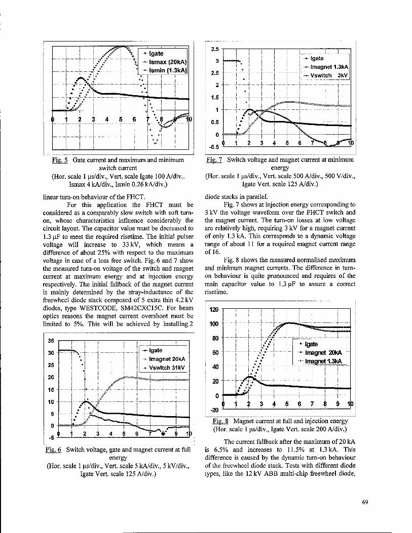
i*&£
— Igate — Ismax (20kA) ^ Ismin (1.3kA)
**&**•
Fig. 5 Gate current and maximum and minimum switch current
(Hör. scale 1 us/div., Vert, scale Igate 100 A/div., Ismax 4 kA/div., Ismin 0.26 kA/div.)
linear turn-on behaviour of the FHCT. For this application the FHCT must be
considered as a comparably slow switch with soft turn- on, whose characteristics influence considerably the circuit layout. The capacitor value must be decreased to 1.3 uF to meet the required risetime. The initial pulser voltage will increase to 33 kV, which means a difference of about 25% with respect to the maximum voltage in case of a loss free switch. Fig. 6 and 7 show the measured turn-on voltage of the switch and magnet current at maximum energy and at injection energy respectively. The initial fallback of the magnet current is mainly determined by the stray-inductance of the freewheel diode stack composed of 5 extra thin 4.2 kV diodes, type WESTCODE, SM42CXC15C. For beam optics reasons the magnet current overshoot must be limited to 5%. This will be achieved by installing 2
Fig. 6 Switch voltage, gate and magnet current at full energy
(Hor. scale 1 us/div., Vert, scale 5 kA/div., 5 kV/div., Igate Vert, scale 125 A/div.)
3.5 -i
3
2.5
2
1.5
1
0.5
0 \
♦
*
i \ \ \ — Igate ^Imagnet 1.3kA — Vswitch 3kV !
*
ECCCO*YJ~~
<^Kj
.JVIC ■ l-gjK
s^ !*•> ♦...
! x
\.
I I k 3 4 5 ( ! y^i^x^i -u.u
Fig. 7 Switch voltage and magnet current at minimum energy
(Hor. scale 1 us/div., Vert, scale 500 A/div., 500 V/div., Igate Vert, scale 125 A/div.)
diode stacks in parallel. Fig. 7 shows at injection energy corresponding to
3 kV the voltage waveform over the FHCT switch and the magnet current. The turn-on losses at low voltage are relatively high, requiring 3 kV for a magnet current of only 1.3 kA. This corresponds to a dynamic voltage range of about 11 for a required magnet current range of 16.
Fig. 8 shows the measured normalised maximum and minimum magnet currents. The difference in turn- on behaviour is quite pronounced and requires of the main capacitor value to 1.3 uF to assure a correct risetime.
120
100
80
60
40
20
0
-20
— Igate — Imagnet 20kA -*- Imagnet 1.3kA
Fig. 8 Magnet current at full and injection energy (Hor. scale 1 us/div., Igate Vert, scale 200 A/div.)
The current fallback after the maximum of 20 kA is 6.5% and increases to 11.5% at 1.3 kA. This difference is caused by the dynamic turn-on behaviour of the freewheel diode stack. Tests with different diode types, like the 12 kV ABB multi-chip freewheel diode,
69
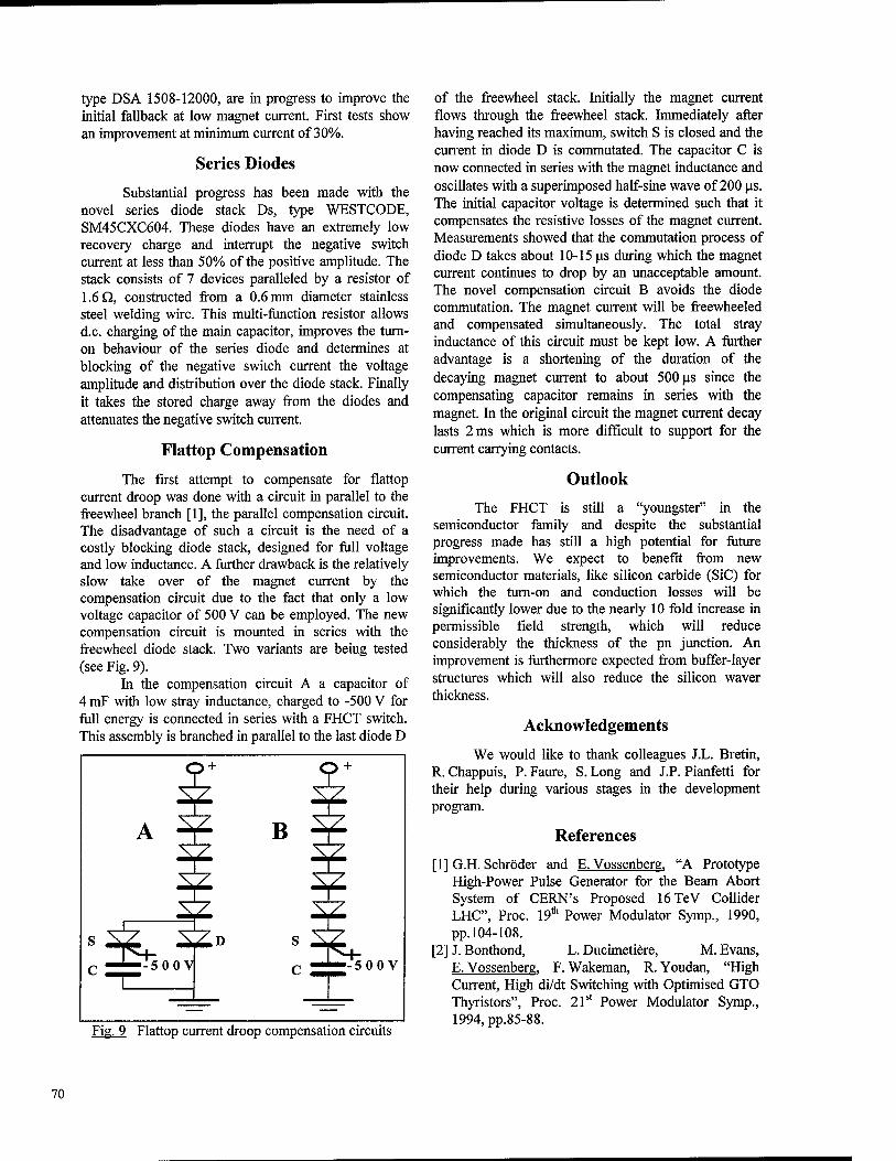
type DSA 1508-12000, are in progress to improve the initial fallback at low magnet current. First tests show an improvement at minimum current of 30%.
Series Diodes
Substantial progress has been made with the novel series diode stack Ds, type WESTCODE, SM45CXC604. These diodes have an extremely low recovery charge and interrupt the negative switch current at less than 50% of the positive amplitude. The stack consists of 7 devices paralleled by a resistor of 1.6 Q, constructed from a 0.6 mm diameter stainless steel welding wire. This multi-function resistor allows d.c. charging of the main capacitor, improves the turn- on behaviour of the series diode and determines at blocking of the negative switch current the voltage amplitude and distribution over the diode stack. Finally it takes the stored charge away from the diodes and attenuates the negative switch current.
Flattop Compensation
The first attempt to compensate for flattop current droop was done with a circuit in parallel to the freewheel branch [1], the parallel compensation circuit. The disadvantage of such a circuit is the need of a costly blocking diode stack, designed for full voltage and low inductance. A further drawback is the relatively slow take over of the magnet current by the compensation circuit due to the fact that only a low voltage capacitor of 500 V can be employed. The new compensation circuit is mounted in series with the freewheel diode stack. Two variants are being tested (see Fig. 9).
In the compensation circuit A a capacitor of 4 mF with low stray inductance, charged to -500 V for full energy is connected in series with a FHCT switch. This assembly is branched in parallel to the last diode D
&
1 1 B
ÄD 500V I* 500V
Fig. 9 Flattop current droop compensation circuits
of the freewheel stack. Initially the magnet current flows through the freewheel stack. Immediately after having reached its maximum, switch S is closed and the current in diode D is commutated. The capacitor C is now connected in series with the magnet inductance and oscillates with a superimposed half-sine wave of 200 (as. The initial capacitor voltage is determined such that it compensates the resistive losses of the magnet current. Measurements showed that the commutation process of diode D takes about 10-15 (as during which the magnet current continues to drop by an unacceptable amount. The novel compensation circuit B avoids the diode commutation. The magnet current will be freewheeled and compensated simultaneously. The total stray inductance of this circuit must be kept low. A further advantage is a shortening of the duration of the decaying magnet current to about 500 |as since the compensating capacitor remains in series with the magnet. In the original circuit the magnet current decay lasts 2 ms which is more difficult to support for the current carrying contacts.
Outlook
The FHCT is still a "youngster" in the semiconductor family and despite the substantial progress made has still a high potential for future improvements. We expect to benefit from new semiconductor materials, like silicon carbide (SiC) for which the turn-on and conduction losses will be significantly lower due to the nearly 10 fold increase in permissible field strength, which will reduce considerably the thickness of the pn junction. An improvement is furthermore expected from buffer-layer structures which will also reduce the silicon waver thickness.
Acknowledgements
We would like to thank colleagues J.L. Bretin, R. Chappuis, P. Faure, S. Long and J.P. Pianfetti for their help during various stages in the development program.
References
[1] G.H. Schröder and E. Vossenberg. "A Prototype High-Power Pulse Generator for the Beam Abort System of CERN's Proposed 16TeV Collider LHC", Proc. 19th Power Modulator Symp., 1990, pp.104-108.
[2] J. Bonthond, L. Ducimetiere, M. Evans, E. Vossenberg. F. Wakeman, R. Youdan, "High Current, High di/dt Switching with Optimised GTO Thyristors", Proc. 21st Power Modulator Symp., 1994, pp.85-88.
70
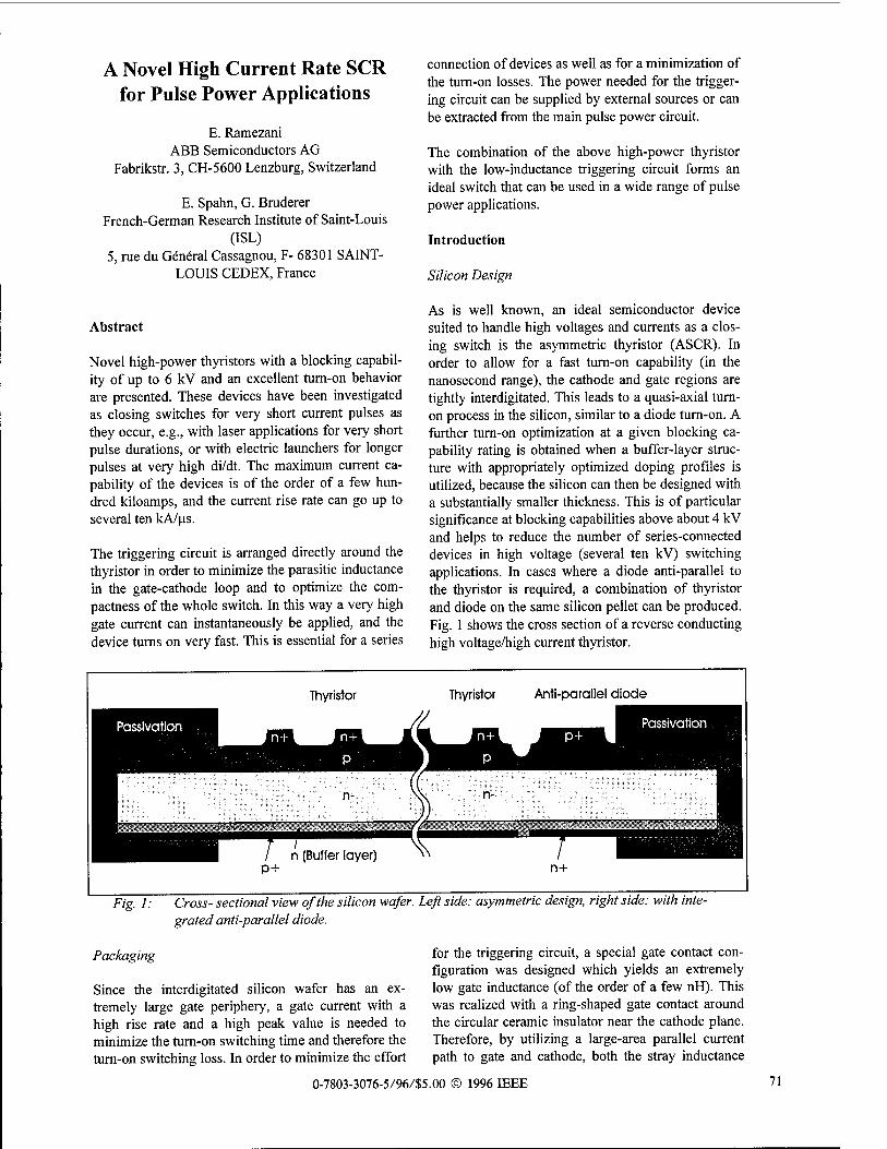
A Novel High Current Rate SCR for Pulse Power Applications
E. Ramezani ABB Semiconductors AG
Fabrikstr. 3, CH-5600 Lenzburg, Switzerland
E. Spahn, G. Bruderer French-German Research Institute of Saint-Louis
(ISL) 5, rue du General Cassagnou, F- 68301 SAINT-
LOUIS CEDEX, France
Abstract
Novel high-power thyristors with a blocking capabil- ity of up to 6 kV and an excellent turn-on behavior are presented. These devices have been investigated as closing switches for very short current pulses as they occur, e.g., with laser applications for very short pulse durations, or with electric launchers for longer pulses at very high di/dt. The maximum current ca- pability of the devices is of the order of a few hun- dred kiloamps, and the current rise rate can go up to several ten kA/us.
The triggering circuit is arranged directly around the thyristor in order to minimize the parasitic inductance in the gate-cathode loop and to optimize the com- pactness of the whole switch. In this way a very high gate current can instantaneously be applied, and the device turns on very fast. This is essential for a series
connection of devices as well as for a minimization of the turn-on losses. The power needed for the trigger- ing circuit can be supplied by external sources or can be extracted from the main pulse power circuit.
The combination of the above high-power thyristor with the low-inductance triggering circuit forms an ideal switch that can be used in a wide range of pulse power applications.
Introduction
Silicon Design
As is well known, an ideal semiconductor device suited to handle high voltages and currents as a clos- ing switch is the asymmetric thyristor (ASCR). In order to allow for a fast turn-on capability (in the nanosecond range), the cathode and gate regions are tightly interdigitated. This leads to a quasi-axial turn- on process in the silicon, similar to a diode turn-on. A further turn-on optimization at a given blocking ca- pability rating is obtained when a buffer-layer struc- ture with appropriately optimized doping profiles is utilized, because the silicon can then be designed with a substantially smaller thickness. This is of particular significance at blocking capabilities above about 4 kV and helps to reduce the number of series-connected devices in high voltage (several ten kV) switching applications. In cases where a diode anti-parallel to the thyristor is required, a combination of thyristor and diode on the same silicon pellet can be produced. Fig. 1 shows the cross section of a reverse conducting high voltage/high current thyristor.
Thyristor Thyristor Anti-parallel diode
Fig. 1:
Packaging
Cross- sectional view of the silicon wafer. Left side: asymmetric design, right side: with inte- grated anti-parallel diode.
Since the interdigitated silicon wafer has an ex- tremely large gate periphery, a gate current with a high rise rate and a high peak value is needed to minimize the turn-on switching time and therefore the turn-on switching loss. In order to minimize the effort
for the triggering circuit, a special gate contact con- figuration was designed which yields an extremely low gate inductance (of the order of a few nH). This was realized with a ring-shaped gate contact around the circular ceramic insulator near the cathode plane. Therefore, by utilizing a large-area parallel current path to gate and cathode, both the stray inductance
0-7803-3076-5/96/S5.00 © 1996 IEEE 71
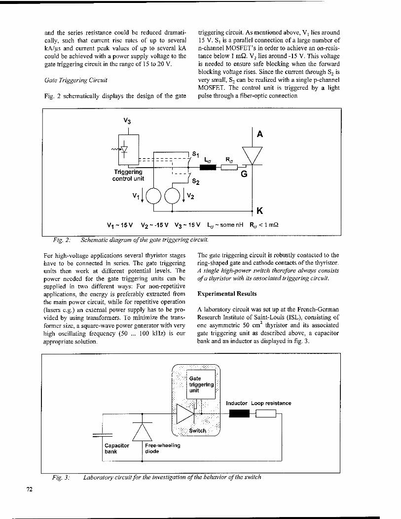
and the series resistance could be reduced dramati- cally, such that current rise rates of up to several kA/us and current peak values of up to several kA could be achieved with a power supply voltage to the gate triggering circuit in the range of 15 to 20 V.
Gate Triggering Circuit
Fig. 2 schematically displays the design of the gate
triggering circuit. As mentioned above, V] lies around 15 V. S[ is a parallel connection of a large number of n-channel MOSFET's in order to achieve an on-resis- tance below 1 mQ. V2 lies around -15 V. This voltage is needed to ensure safe blocking when the forward blocking voltage rises. Since the current through S2 is very small, S2 can be realized with a single p-channel MOSFET. The control unit is triggered by a light pulse through a fiber-optic connection
V3
Triggering control unit
V1
Si
s2
v2
K
V.J-15V V2~-15V V3~15V L^-somenH Ra < 1 mfi
Fig. 2: Schematic diagram of the gate triggering circuit.
For high-voltage applications several thyristor stages have to be connected in series. The gate triggering units then work at different potential levels. The power needed for the gate triggering units can be supplied in two different ways: For non-repetitive applications, the energy is preferably extracted from the main power circuit, while for repetitive operation (lasers e.g.) an external power supply has to be pro- vided by using transformers. To minimize the trans- former size, a square-wave power generator with very high oscillating frequency (50 ... 100 kHz) is our appropriate solution.
The gate triggering circuit is robustly contacted to the ring-shaped gate and cathode contacts of the thyristor. A single high-power switch therefore always consists of a thyristor with its associated triggering circuit.
Experimental Results
A laboratory circuit was set up at the French-German Research Institute of Saint-Louis (ISL), consisting of one asymmetric 50 cm thyristor and its associated gate triggering unit as described above, a capacitor bank and an inductor as displayed in fig. 3.
Gate triggering unit
Inductor Loop resistance
, Switch i
Capacitor bank
Free-wheeling diode
Fig. 3: Laboratory circuit for the investigation of the behavior of the switch
72
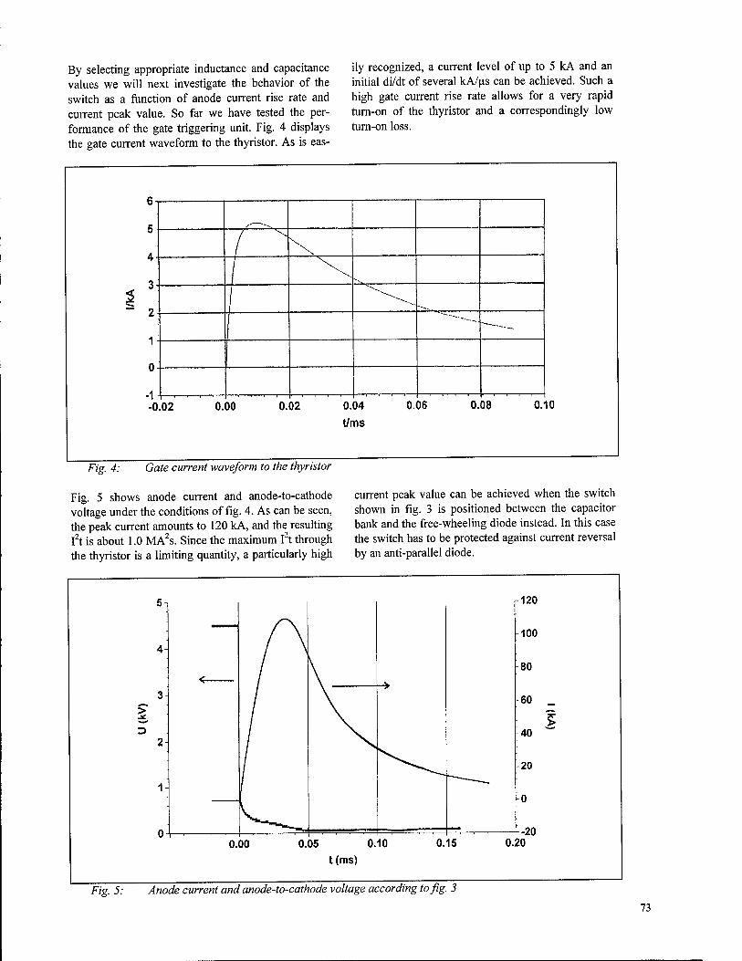
By selecting appropriate inductance and capacitance values we will next investigate the behavior of the switch as a function of anode current rise rate and current peak value. So far we have tested the per- formance of the gate triggering unit. Fig. 4 displays the gate current waveform to the thyristor. As is eas-
ily recognized, a current level of up to 5 kA and an initial di/dt of several kA/us can be achieved. Such a high gate current rise rate allows for a very rapid turn-on of the thyristor and a correspondingly low turn-on loss.
Fig. 4: Gate current waveform to the thyristor
Fig. 5 shows anode current and anode-to-cathode voltage under the conditions of fig. 4. As can be seen, the peak current amounts to 120 kA, and the resulting I2t is about 1.0 MA2s. Since the maximum ft through the thyristor is a limiting quantity, a particularly high
current peak value can be achieved when the switch shown in fig. 3 is positioned between the capacitor bank and the free-wheeling diode instead. In this case the switch has to be protected against current reversal by an anti-parallel diode.
Fig. 5: Anode current and anode-to-cathode voltage according to fig. 3
73
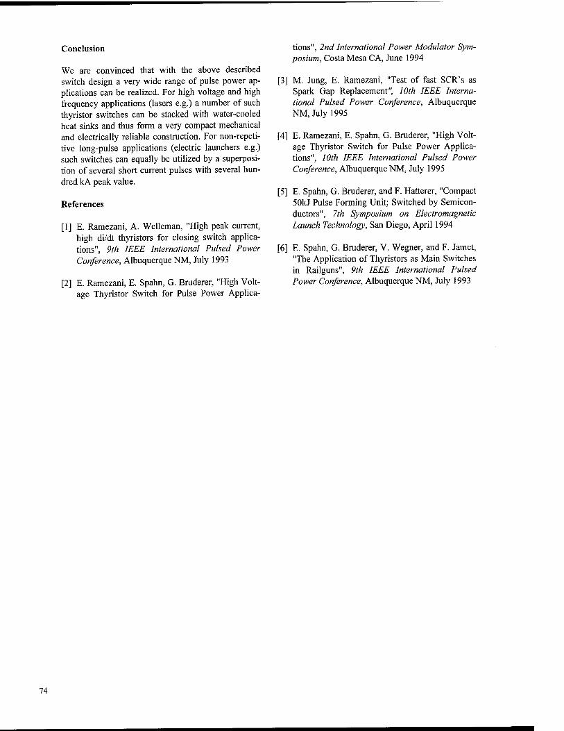
Conclusion
We are convinced that with the above described switch design a very wide range of pulse power ap- plications can be realized. For high voltage and high frequency applications (lasers e.g.) a number of such thyristor switches can be stacked with water-cooled heat sinks and thus form a very compact mechanical and electrically reliable construction. For non-repeti- tive long-pulse applications (electric launchers e.g.) such switches can equally be utilized by a superposi- tion of several short current pulses with several hun- dred kA peak value.
References
[1] E. Ramezani, A. Welleman, "High peak current, high di/dt thyristors for closing switch applica- tions", 9th IEEE International Pulsed Power Conference, Albuquerque NM, July 1993
[2] E. Ramezani, E. Spahn, G. Bruderer, "High Volt- age Thyristor Switch for Pulse Power Applica-
tions", 2nd International Power Modulator Sym- posium, Costa Mesa CA, June 1994
[3] M. Jung, E. Ramezani, "Test of fast SCR's as Spark Gap Replacement", 10th IEEE Interna- tional Pulsed Power Conference, Albuquerque NM, July 1995
[4] E. Ramezani, E. Spahn, G. Bruderer, "High Volt- age Thyristor Switch for Pulse Power Applica- tions", 10th IEEE International Pulsed Power Conference, Albuquerque NM, July 1995
[5] E. Spahn, G. Bruderer, and F. Härterer, "Compact 50kJ Pulse Forming Unit; Switched by Semicon- ductors", 7th Symposium on Electromagnetic Launch Technology, San Diego, April 1994
[6] E. Spahn, G. Bruderer, V. Wegner, and F. Jamet, "The Application of Thyristors as Main Switches in Railguns", 9th IEEE International Pulsed Power Conference, Albuquerque NM, July 1993
74
BIOFOULING PREVENTION WITH PULSED ELECTRIC FIELDS
Karl H. Schoenbach, Raymond W. Aldert III* Physical Electronics Research Institute/ 'Applied Marine Research Laboratory
Old Dominion University, Norfolk, VA 23529 and
Thomas J. Fox Center for Advanced Ship Repair and Maintenance (CASRM), Norfolk, VA 23510
Abstract
Clogging of pipes due to biofouling organisms capable of rapid population growth is a major problem in cooling systems where untreated lake, river or sea water is used. In estuarine and marine ecosystems it is blue mussels and barnacles which cause biofouling problems, in freshwater ecosystems the uncontrolled growth of zebra mussels has significant economic implications. In order to explore the preventive effect of pulsed electric fields on biofoulants, we have, following laboratory studies [1], performed field tests with a pulse power system which was to designed to provide \i$ pulses of up to 40 kV into a low impedance (< 10 Q) load. The system was used to treat water from the Elizabeth River in Norfolk. Two tests, each performed over a period of three weeks with pulsed electric fields of 12 kV/cm, and 6.4 kV/cm, respectively, in the treatment cell have demonstrated the feasibility of the electric field method for biofouling prevention. Whereas strong growth of barnacles, blue mussels and hydrazoans was seen in the control system, the test system was completely free of these biofoulants. The highest efficiency reached so far was 1,400 gallons of treated tidal water per kWh of electrical energy. It is expected that the efficiency can be further increased by optimizing the effect with respect to pulse duration and electric field, and by concentrating on fresh water biofoulants, such as zebra mussels.
Introduction
Biofouling of cooling water systems is caused by the settling of micro-organisms which are floating in the cooling water, e.g. larvae of mussels, on the walls of the pipes. Their growth at the pipe surface impedes the flow of cooling water, and eventually may clog the pipes. Techniques to prevent the growth are use of chemicals or flushing the pipes with hot water. The removal of the biomass requires acoustic shock treatment or mechanical techniques.
Based on experiments on the effect of electric fields on bacteria we have explored the use of an electro technology for the prevention of biofouling: the pulsed electric field technique (PEFT). The water containing biofoulants is exposed to pulsed electric fields before it enters the cooling system. Pulsed electric fields are known to cause lysing of bacteria if the field amplitude exceeds a threshold value. We have, however, mainly concentrated on non lethal effects induced by electric fields below the threshold for lysing. These effects lead only to a temporal inability of the micro-organism to attach to the pipes. This is desirable for two reason: it does not affect the ecological system, and it reduces the energy cost for the prevention of biofouling.
The pulse power system used for field tests is shown schematically in Fig. 1: It consists of a pulse forming network (PFN) arranged in a Blumlein configuration. The PFN is charged by means of a power supply (not shown in this figure) and discharged by means of a thyratron into a treatment cell, consisting of water between two metal electrodes. The value of the electric field in the water which contains the micro- organisms is given as the applied voltage divided by the distance between the electrodes.
Effect of Pulsed Electric Fields on Cells
The application of electric fields to living cells in a suspending medium causes a buildup of electrical charges at the cell membrane, and consequently a change in the voltage across the membrane. For low electric fields this initiates voltage gating, a voltage induced opening of channels in the cell membrane. The flux of ions, such as sodium or potassium ions, through the channels changes the ion concentrations close to the cell membrane. This imbalance in ion concentration is a cause of stress for the micro- organism. At higher electric fields, and correspondingly higher voltages across the cell
0-7803-3076-5/96/S5.00 © 1996 IEEE 75
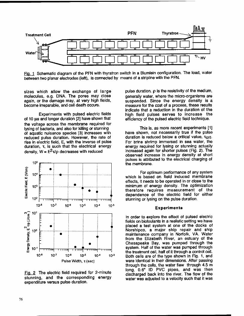
Treatment Cell
\
PFN Thyratron —___^ Ml
3E HE 3L
~±
_J ^ HV
Rq. 1 Schematic diagram of the PFN with thyratron switch in a Blumlein configuration. The load, water between two planar electrodes (left), is connected by means of a stripline with the PFN.
sizes which allow the exchange of large molecules, e.g. DNA. The pores may close again, or the damage may, at very high fields, become irreparable, and cell death occurs.
Experiments with pulsed electric fields of 10 \xs and longer duration [2] have shown that the voltage across the membrane required for lysing of bacteria, and also for killing or stunning of aquatic nuisance species [3] increases with reduced pulse duration. However, the rate of rise in electric field, E, with the inverse of pulse duration, x, is such that the electrical energy density, W = E^/p decreases with reduced
10s
E" .o £ 10"
2 a) il 103 u
102 i i i null I I i null i i 11HIM i i 11HIM—i i i inn
10-8 10-7 10-6 10-5 TCH 10-3
10-8 10-7 10-6 10s 10-4 10-3
Pulse Width, T (sec)
Fig. 2 The electric field required for 2-minute stunning, and the corresponding energy expenditure versus pulse duration.
pulse duration, p is the resistivity of the medium, generally water, where the micro-organisms are suspended. Since the energy density is a measure for the cost of a process, these results indicate that a reduction in the duration of the high field pulses serves to increase the efficiency of the pulsed electric field technique.
This is, as more recent experiments [1] have shown, not necessarily true if the pulse duration is reduced below a critical value, Xcrit- For brine shrimp immersed in sea water, the energy required for lysing or stunning actually increased again for shorter pulses (Fig. 2). The observed increase in energy density at short pulses is attributed to the electrical charging of the membrane.
For optimum performance of any system which is based on field induced membrane effects, it needs to be operated in or close to the minimum of energy density. The optimization therefore requires measurement of the dependence of the electric field for either stunning or lysing on the pulse duration.
Experiments
In order to explore the effect of pulsed electric fields on biofoulants in a realistic setting we have placed a test system at one of the docks of Norshipco, a major ship repair and ship maintenance company in Norfolk, VA. Water from the Elizabeth River, an estuary of the Chesapeake Bay, was pumped through the system. Half of the water was pumped through the treatment cell, half of it through a control cell. Both cells are of the type shown in Fig. 1, and were identical in their dimensions. After passing through the cells, the water flew through 4.5 m long, 0.6" ID PVC pipes, and was then discharged back into the river. The flow of the water was adjusted to a velocity such that it was
76
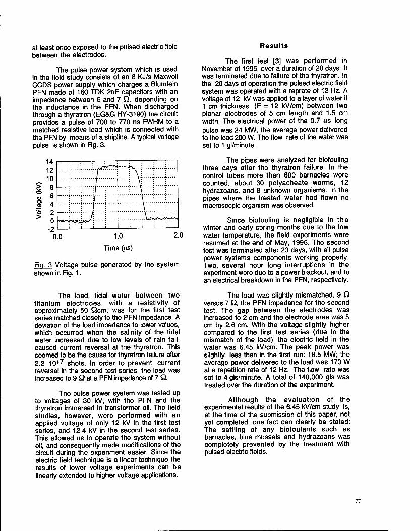
at least once exposed to the pulsed electric field between the electrodes.
The pulse power system which is used in the field study consists of an 8 KJ/s Maxwell CCDS power supply which charges a Blumlein PFN made of 160 TDK 2nF capacitors with an impedance between 6 and 7 Q, depending on the inductance in the PFN. When discharged through a thyratron (EG&G HY-3190) the circuit provides a pulse of 700 to 770 ns FWHM to a matched resistive load which is connected with the PFN by means of a stripline. A typical voltage pulse is shown in Fig. 3.
Time (us)
Fig. 3 Voltage pulse generated by the system shown in Fig. 1.
The load, tidal water between two titanium electrodes, with a resistivity of approximately 50 Qcm, was for the first test series matched closely to the PFN impedance. A deviation of the load impedance to lower values, which occurred when the salinity of the tidal water increased due to low levels of rain fall, caused current reversal at the thyratron. This seemed to be the cause for thyratron failure after 2.2 10+7 shots. In order to prevent current reversal in the second test series, the load was increased to 9 Q at a PFN impedance of 7 Q.
The pulse power system was tested up to voltages of 30 kV, with the PFN and the thyratron immersed in transformer oil. The field studies, however, were performed with an applied voltage of only 12 kV in the first test series, and 12.4 kV in the second test series. This allowed us to operate the system without oil, and consequently made modifications of the circuit during the experiment easier. Since the electric field technique is a linear technique the results of lower voltage experiments can be linearly extended to higher voltage applications.
Results
The first test [3] was performed in November of 1995, over a duration of 20 days. It was terminated due to failure of the thyratron. In the 20 days of operation the pulsed electric field system was operated with a reprate of 12 Hz. A voltage of 12 kV was applied to a layer of water if 1 cm thickness (E = 12 kV/cm) between two planar electrodes of 5 cm length and 1.5 cm width. The electrical power of the 0.7 us long pulse was 24 MW, the average power delivered to the load 200 W. The flow rate of the water was set to 1 gl/minute.
The pipes were analyzed for biofouling three days after the thyratron failure. In the control tubes more than 600 barnacles were counted, about 30 polyacheate worms, 12 hydrazoans, and 8 unknown organisms. In the pipes where the treated water had flown no macroscopic organism was observed.
Since biofouling is negligible in the winter and early spring months due to the low water temperature, the field experiments were resumed at the end of May, 1996. The second test was terminated after 23 days, with all pulse power systems components working properly. Two, several hour long interruptions in the experiment were due to a power blackout, and to an electrical breakdown in the PFN, respectively.
The load was slightly mismatched, 9 Q versus 7 Q, the PFN impedance for the second test. The gap between the electrodes was increased to 2 cm and the electrode area was 5 cm by 2.6 cm. With the voltage slightly higher compared to the first test series (due to the mismatch of the load), the electric field in the water was 6.45 kV/cm. The peak power was slightly less than in the first run: 18.5 MW; the average power delivered to the load was 170 W at a repetition rate of 12 Hz. The flow rate was set to 4 gls/minute. A total of 140,000 gls was treated over the duration of the experiment.
Although the evaluation of the experimental results of the 6.45 kV/cm study is, at the time of the submission of this paper, not yet completed, one fact can clearly be stated: The settling of any biofoulants such as barnacles, blue mussels and hydrazoans was completely prevented by the treatment with pulsed electric fields.
77

Conclusions
A suggested definition for the efficiency of the pulsed electric field method is the volume of successfully treated water per electrical energy unit, e.g. number of gallons of treated water per kWh electrical energy. In other words, efficiency is defined as the inverse of the energy density dissipated in the water. Using the results of the second experiment, where an electrical field of 6.45 kV/cm of 770 ns duration was sufficient to prevent blue mussel, barnacle and hydrazoan biofouling in pipes, the efficiency is at least 1,400 gls/kWh.
If we use this number to determine the electrical power required to treat all the cooling water of a power plant, with an assumed water flow of one million gallons per minute, the value is 42.5 MW. This is definitely out of range for treatment of biofouling. However, there are three reasons that this number can be dramatically reduced:
1. We have, at this particular pulse duration of 770 ns, not yet reached the minimum electric field required to stun biofoulants.
2. It is also very unlikely that we have reached the minimum in the energy-pulse duration curve (see Fig. 2) for stunning of biofoulants.
3. The experiments were so far performed in tidal water, a medium with relatively high conductivity. One of the major threats to cooling systems, however, is a fresh water nuisance species, the zebra mussel. Experimental results with bacteria indicate that the application of the pulse field effect to fresh water, with lower conductivity, leads to an increase in efficiency.
Taking this into account, it should be possible to increase the efficiency for the treatment of fresh water biofoulants by at least two orders of magnitude compared to the present value. This would reduce the power consumption for an electrical filter in a power plant with one million gallons per minute to values on the order of several hundred kW, a reasonable value.
Even if the predicted efficiency cannot be reached, the use of pulsed electric field systems at the present state of development might already be economically feasible for small cooling water systems, which are difficult to clean. The advantages over other techniques used for biofouling prevention such as
its independence from chemicals,
• the fact that it is possible to stun, rather than kill unwanted biofouling species,
• that it does not generate shock waves which could affect the structure of the cooling system, and
• that it can be installed like a filter in front of an existing cooling system, without requiring any changes in the cooling system,
make the pulsed electric field technology (PEFT) a strong contender to existing biofouling prevention methods.
Acknowledgments
This work was supported by the Center for Advanced Ship Repair and Maintenance (CASRM), a Consortium consisting of the Office of Naval Research, Commonwealth of Virginia, City of Norfolk, Old Dominion University and the South Tidewater Association of Ship Repairers.
References
1. K.H. Schoenbach, F.E. Peterkin, S. Beebe, D. Byars, R. Alden, P. Adolphson, and T. Turner, "Effect of Pulsed Electric Fields on Micro-Organisms: Experiments and Applications," Proc. 10th Intern. Pulsed Power Conf., Albuquerque, NM, June 1995.
2. H. Huelsheger, J. Potel, and E.G. Niemann, "Killing of Bacteria with Electric Pulses of High Electric Field Strength," Radiat. Environ. Biophys. 20, 53(1981).
3. J.R. Duncan, M. Rader, S. Levy, I. Alexeff, J.A. Drake, and J. Johnson, "The Use of Pulse Power to Control Zebra Mussels," Proc. Third Intern. Zebra Mussel Conf., Toronto, Ontario, Canada.
4. K.H. Schoenbach, R.W. Alden, and T.J. Fox, "Effect of Pulsed Electric Fields on Aquatic Nuisance Species," to appear in Zebra Mussels and other Aquatic Nuisance Species. Frank D'ltri, ed., Ann Arbor Press, Inc., Chelsea, Ml.
78
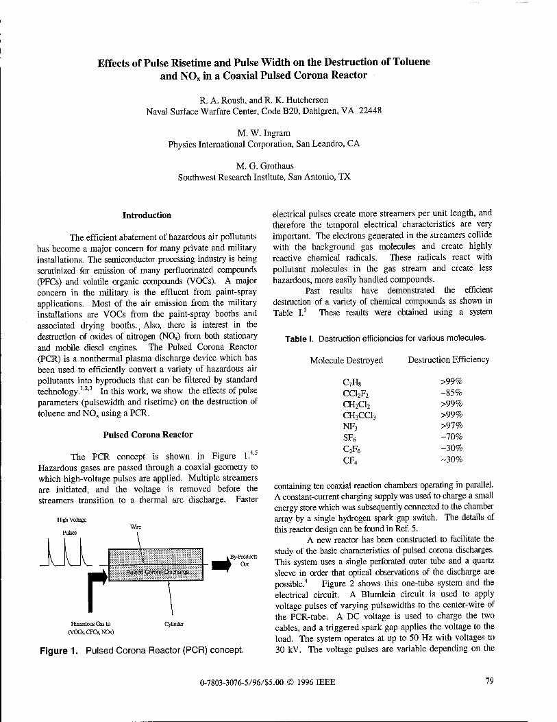
Effects of Pulse Risetime and Pulse Width on the Destruction of Toluene and NOx in a Coaxial Pulsed Corona Reactor
R. A. Roush, and R. K. Hutcherson Naval Surface Warfare Center, Code B20, Dahlgren, VA 22448
M. W. Ingram Physics International Corporation, San Leandro, CA
M. G. Grothaus Southwest Research Institute, San Antonio, TX
Introduction
The efficient abatement of hazardous air pollutants has become a major concern for many private and military installations. The semiconductor processing industry is being scrutinized for emission of many perfluorinated compounds (PFCs) and volatile organic compounds (VOCs). A major concern in the military is the effluent from paint-spray applications. Most of the air emission from the military installations are VOCs from the paint-spray booths and associated drying booths., Also, there is interest in the destruction of oxides of nitrogen (NOx) from both stationary and mobile diesel engines. The Pulsed Corona Reactor (PCR) is a nonthermal plasma discharge device which has been used to efficiently convert a variety of hazardous air pollutants into byproducts that can be filtered by standard technology.1,2,3 In this work, we show the effects of pulse parameters (pulsewidth and risetime) on the destruction of toluene and NOx using a PCR.
Pulsed Corona Reactor
The PCR concept is shown in Figure I.4'5
Hazardous gases are passed through a coaxial geometry to which high-voltage pulses are applied. Multiple streamers are initiated, and the voltage is removed before the streamers transition to a thermal arc discharge. Faster
High Voltage
Pulses Wire
X1L r Pulsed Corona Discharge
^ By-Products Out
Hazardous Gas In
(VOCs, CFCs, NOx)
Cylinder
electrical pulses create more streamers per unit length, and therefore the temporal electrical characteristics are very important. The electrons generated in the streamers collide with the background gas molecules and create highly reactive chemical radicals. These radicals react with pollutant molecules in the gas stream and create less hazardous, more easily handled compounds.
Past results have demonstrated the efficient destruction of a variety of chemical compounds as shown in Table I.5 These results were obtained using a system
Table I. Destruction efficiencies for various molecules.
Molecule Destroyed Destruction Efficiency
C7H8 >99% CC12F2 -85% CH2C12 >99% CH3CCI3 >99%
NF3 >97%
SF6 -70% C2F6 -30% CF4 -30%
Figure 1. Pulsed Corona Reactor (PCR) concept.
containing ten coaxial reaction chambers operating in parallel. A constant-current charging supply was used to charge a small energy store which was subsequently connected to the chamber array by a single hydrogen spark gap switch. The details of this reactor design can be found in Ref. 5.
A new reactor has been constructed to facilitate the study of the basic characteristics of pulsed corona discharges. This system uses a single perforated outer tube and a quartz sleeve in order that optical observations of the discharge are possible.4 Figure 2 shows this one-tube system and the electrical circuit. A Blumlein circuit is used to apply voltage pulses of varying pulsewidths to the center-wire of the PCR-tube. A DC voltage is used to charge the two cables, and a triggered spark gap applies the voltage to the load. The system operates at up to 50 Hz with voltages to 30 kV. The voltage pulses are variable depending on the
0-7803-3076-5/96/S5.00 © 1996 IEEE 79
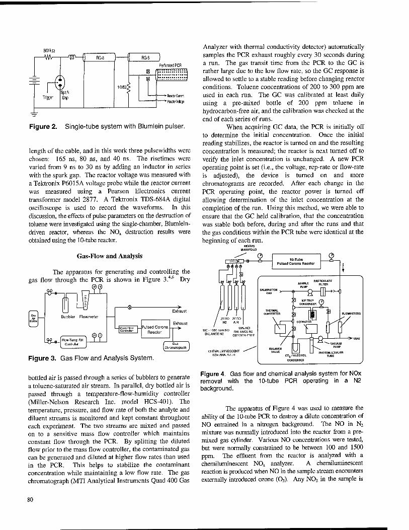
500 kO
i—VW
Figure 2. Single-tube system with Blumlein pulser.
length of the cable, and in this work three pulsewidths were chosen: 165 ns, 80 ns, and 40 ns. The risetimes were varied from 9 ns to 30 ns by adding an inductor in series with the spark gap. The reactor voltage was measured with a Tektronix P6015A voltage probe while the reactor current was measured using a Pearson Electronics current transformer model 2877. A Tektronix TDS-684A digital oscilloscope is used to record the waveforms. In this discussion, the effects of pulse parameters on the destruction of toluene were investigated using the single-chamber, Blumlein- driven reactor, whereas the NOx destruction results were obtained using the 10-tube reactor.
Analyzer with thermal conductivity detector) automatically samples the PCR exhaust roughly every 30 seconds during a run. The gas transit time from the PCR to the GC is rather large due to the low flow rate, so the GC response is allowed to settle to a stable reading before changing reactor conditions. Toluene concentrations of 200 to 300 ppm are used in each run. The GC was calibrated at least daily using a pre-mixed bottle of 200 ppm toluene in hydrocarbon-free air, and the calibration was checked at the end of each series of runs.
When acquiring GC data, the PCR is initially off to determine the initial concentration. Once the initial reading stabilizes, the reactor is turned on and the resulting concentration is measured; the reactor is next turned off to verify the inlet concentration is unchanged. A new PCR operating point is set (i.e., the voltage, rep-rate or flow-rate is adjusted), the device is turned on and more chromatograms are recorded. After each change in the PCR operating point, the reactor power is turned off allowing determination of the inlet concentration at the completion of the run. Using this method, we were able to ensure that the GC held calibration, that the concentration was stable both before, during and after the runs and that the gas conditions within the PCR tube were identical at the beginning of each run.
Gas-Flow and Analysis
The apparatus for generating and controlling the 4,6 gas flow through the PCR is shown in Figure 3. ' Dry
Bubbler Flowmeter
W_a_ Flow-Temp-RH
^ Controller 11
Exhaust
Pulsed Corona Reactor
f Gas l Chromatograph
Figure 3. Gas Flow and Analysis System.
bottled air is passed through a series of bubblers to generate a toluene-saturated air stream. In parallel, dry bottled air is passed through a temperature-flow-humidity controller (Miller-Nelson Research Inc. model HCS-401). The temperature, pressure, and flow rate of both the analyte and diluent streams is monitored and kept constant throughout each experiment. The two streams are mixed and passed on to a sensitive mass flow controller which maintains constant flow through the PCR. By splitting the diluted flow prior to the mass flow controller, the contaminated gas can be generated and diluted at higher flow rates than used in the PCR. This helps to stabilize the contaminant concentration while maintaining a low flow rate. The gas Chromatograph (MTI Analytical Instruments Quad 400 Gas
10-Tube
Pulsed Corona Reactor
100-1000 ppm NO BALANCE N2
CH EMILUMINESCENT NOx ANALYZER
PARTICULATE SAMPLE „(.re,,
FLOWMETERS
C02/ALCOHOL
CONDENSER
l_l PHOTOMULTIPUER TUBE
Figure 4. Gas flow and chemical analysis system for NOx removal with the 10-tube PCR operating in a N2 background.
The apparatus of Figure 4 was used to measure the ability of the 10-tube PCR to destroy a dilute concentration of NO entrained in a nitrogen background. The NO in N2
mixture was normally introduced into the reactor from a pre- mixed gas cylinder. Various NO concentrations were tested, but were normally constrained to be between 100 and 1500 ppm. The effluent from the reactor is analyzed with a chemiluminescent NOx analyzer. A chemiluminescent reaction is produced when NO in the sample stream encounters externally introduced ozone (03). Any N02 in the sample is
80
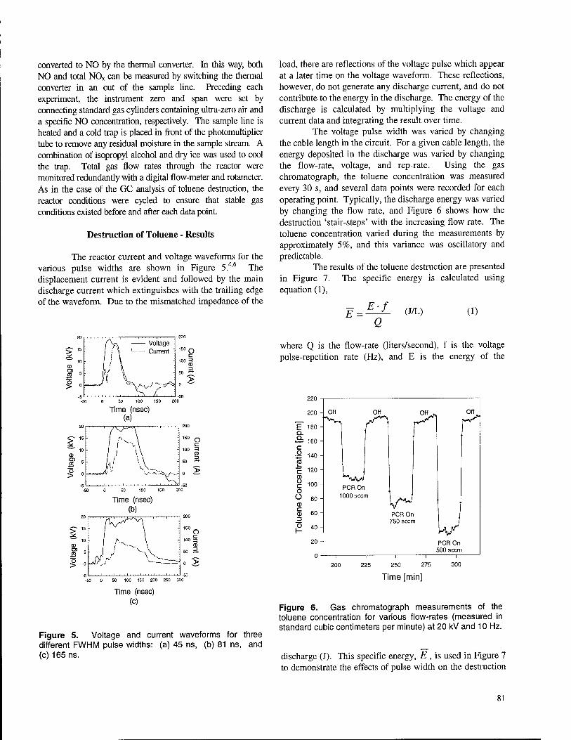
converted to NO by the thermal converter. In this way, both NO and total NOx can be measured by switching the thermal converter in an out of the sample line. Preceding each experiment, the instrument zero and span were set by connecting standard gas cylinders containing ultra-zero air and a specific NO concentration, respectively. The sample line is heated and a cold trap is placed in front of the photomultiplier tube to remove any residual moisture in the sample stream. A combination of isopropyl alcohol and dry ice was used to cool the trap. Total gas flow rates through the reactor were monitored redundantly with a digital flow-meter and rotameter. As in the case of the GC analysis of toluene destruction, the reactor conditions were cycled to ensure that stable gas conditions existed before and after each data point.
Destruction of Toluene - Results
The reactor current and voltage waveforms for the various pulse widths are shown in Figure 5.4,6 The displacement current is evident and followed by the main discharge current which extinguishes with the trailing edge of the waveform. Due to the mismatched impedance of the
50 100 150
Time (nsec) (a)
Time (nsec) (b)
50 100 150 200 250 300
Time (nsec) (c)
Figure 5. Voltage and current waveforms for three different FWHM pulse widths: (a) 45 ns, (b) 81 ns, and (c) 165 ns.
load, there are reflections of the voltage pulse which appear at a later time on the voltage waveform. These reflections, however, do not generate any discharge current, and do not contribute to the energy in the discharge. The energy of the discharge is calculated by multiplying the voltage and current data and integrating the result over time.
The voltage pulse width was varied by changing the cable length in the circuit. For a given cable length, the energy deposited in the discharge was varied by changing the flow-rate, voltage, and rep-rate. Using the gas Chromatograph, the toluene concentration was measured every 30 s, and several data points were recorded for each operating point. Typically, the discharge energy was varied by changing the flow rate, and Figure 6 shows how the destruction 'stair-steps' with the increasing flow rate. The toluene concentration varied during the measurements by approximately 5%, and this variance was oscillatory and predictable.
The results of the toluene destruction are presented in Figure 7. The specific energy is calculated using equation (1),
E = E-f
Q (J/L) (1)
where Q is the flow-rate (liters/second), f is the voltage pulse-repetition rate (Hz), and E is the energy of the
c CD o c o O
CD C 0 _3 O
220
200
180
160
140
120
100
80
60
40
20
0
Off Off
rO rh
PCROn lOOOsccrm
PCROn 750 seem
Off
rl
225 250 300
Time [min]
Figure 6. Gas Chromatograph measurements of the toluene concentration for various flow-rates (measured in standard cubic centimeters per minute) at 20 kV and 10 Hz.
discharge (J). This specific energy, E, is used in Figure 7 to demonstrate the effects of pulse width on the destruction
81
of toluene. The values of ß shown in Figure 7 are calculated assuming an exponential relationship between destruction and specific energy7,
% destroyed = 100(xrXf)/Xi = 100(l-exp(-£7ß)) (2)
where X; is the initial concentration, xf is the final concentration, and ß is the fitting parameter. The ß-value is used as a figure-of-merit for the destruction of different gases.
determined the destruction level, primarily. Further experiments are required with pulse risetimes in the range of 1-10 ns.
100 • • • i \ i > • • i ii ' '
^-—"— —3~ / s"
/ms *•■-" 75 - />X :
/ / ••■" ±
■ /,v 50 _ / / A*
A * •■•' 7 / A
- /A4 ://A
Ise Width FWHM • '5 -
-///* • 45 ns -
¥ ■ 81 ns - A 165 ns .
ni i ' ' i i i i i i i i i i i
100 200 300 400 500 600
Specific Energy [J/L]
700 800
Figure 7. Destruction of toluene (200 ppm) for various pulse widths. The ß-values are 91 J/L (solid line), 158 J/L (dashed line), and 253 J/L (dotted line).
Another important parameter is the pulse risetime. We have changed the risetime of our voltage pulse in order to determine the effect on destruction. An inductor was added to the circuit in order to change the risetime, but it should be noted that changing the cable lengths also changed the risetime. The risetimes for the three pulse widths described above were 9 ns, 15 ns, and 25 ns for the 45 ns, 81 ns, and 165 ns pulse widths respectively. The destruction efficiency was greater for smaller pulse widths which also corresponded to a shorter risetime. Therefore, an inductor was inserted into the circuit such that the pulse risetime was measured to be 30 ns. Using the same cable as that used to produce the 80 ns pulse width, the added inductance caused the pulse to broaden to 115 ns, FWHM.
This longer risetime pulse was used to destroy toluene, and the results demonstrate that the destruction is not strongly dependent on risetimes in the range tested here (10-30 ns). Figure 8 summarizes the results by showing that the ß-value is a strong function of pulse width. As shown, the 115 ns pulse width (longest risetime, 30 ns) gives better destruction efficiency (lower ß) than the shorter risetime, longer pulse. In our experiments, the pulse width
20 40 60 80 100 120 140 160 180
Pulse Width FWHM [ns]
Figure 8. Effects of the pulse width on the ß-value for toluene. The symbols correspond to those in Figure 7, and the black-diamond represents a 115 ns FWHM, 30 ns risetime pulse.
NO Destruction in N2 - Results
The 10-tube prototype reactor was used to determine the effects of pulse width on the destruction efficiency in NOx
waste-streams. The destruction of NO in a N2 background serves as an initial baseline condition for the more complicated chemistries occurring in dry air, moist air, and diesel exhaust flow streams. Rather than being driven by a cable-type pulser with a characteristic pulse width, the 10-tube reactor employs an RC-type discharge where the pulse width is primarily determined by the size of a lumped storage capacitance. Three cases were studied which corresponded to three different values of primary storage capacitance: 2 nF, 1.4 nF, and 700 pF. As discussed previously5, the voltage and current waveforms are the result of both displacement and conduction contributions measured at the input to the reactor. An increase in storage capacitance extends the tail of the waveform as shown in Figure 9 (top). The time integration of the voltage-current product yields the energy per pulse, and using equations (1) and (2), the plot of Figure 10 results. The plot shows the relative destruction of approximately 100 ppm NO vs. specific energy density in Joules/liter. The pulse width is arbitrarily, but consistently, defined for the three capacitance values as the 10-90% risetime in the energy pulse. It is understood that the energy risetime for a square pulse is equal to the voltage pulse width, and therefore a consistent comparison between the results of the Blumlein-driven circuit and 10-tube system can be made. Previously reported results by Penetrante3 are also shown for comparison.
As in the case of the toluene data in the previous section, the efficiency with which NO is removed is strongly
82
dependent on the width of the applied voltage pulse. The smallest capacitance (pulse width) yields the superior beta value.
-25 25
| I I I I | I M I | I I I I | I
50 75 100 125 150
Time (ns)
c S>
Ü
O to 0)
DC I I I " I" ' I I I I . ! I I
50 75 100 125 150
Time (ns)
i " " i " " i " " r ' " r
-25 0 25 50 75 100 125 150
Time (ns)
Figure 9. Voltage, current, and energy waveforms for the three different primary capacitance values in the 10- tube reactor. The pulse width is defined as the 10-90% risetime of the energy waveform.
Conclusions
The data presented here shows that the destruction of both toluene and NO are strong functions of the electrical pulse width. The destruction was quantified by
a c o o
w CD Q
10 20 30 40 50 60
Energy Density (J/L)
Figure 10. Destruction of NO in N2 for various pulse widths. Pulse width is defined as in Figure 9, and associated b-values are also shown.
an exponential curve fit in which the slope of the curve is used as a figure-of-merit. The inverse of the slope was called the ß-value which was shown to vary with pulse width. Our results demonstrate that the ß-value is not constant for different pulse parameters; contrary to that which has been previously suggested.3 It is important to emphasize that a reduction in pulse width causes an increase in destruction efficiency for both toluene and NO. There are several possible reasons for the pulse parameter dependence of destruction efficiency such as the thermalization of the streamer electrons in the discharge which can occur with long pulse widths. Electrons of an energy necessary to mediate the destruction process are created early in the streamer development process so that added thermalization of the channel via long pulse width wastes energy. Also, the destruction of molecules depends heavily on chemical reactions that occur after the discharge extinguishes. Therefore, there are potentially many 'undesired' chemical species formed with longer pulse widths. In all, nonthermal plasma devices such as the PCR and the silent-discharge reactor7 have demonstrated a unique ability to destroy a wide variety of pollutant compounds. However, continued progress in flow-rate capacity, energy consumption, and by-product identification will be necessary to effectively demonstrate industrial viability for the technology. The present work has shown that a distinct advantage in destruction efficiency can be achieved with a PCR-based system which uses very short, fast-rising voltage pulses.
83
References
1. B. M. Penetrante and S. E. Shultheis, eds., Non-Thermal Plasma Techniques for Pollution Control, Berlin: Springer-Verlag, 1993.
2. T. Yamamoto, K. Ramanathan, P.A. Lawless, D. S. Ensor, J. R. Newsome, N. Plaks, and G. H. Ramsey, "Control of Volatile Organic compounds by an AC- Energized Ferroelectric Pellet Reactor and a Pulsed Corona Reactor." IEEE Transactions on Industry Applications. v28, no.3, pp. 528-534, 1992.
3. B. M. Penetrante, M. C. Hsaio, B. T. Merritt, G. E. Vogtlin, and P. H. Wallman, "Comparison of Electrical Discharge Techniques for Nonthermal Plasma Processing of NO in N2," IEEE Transactions on Plasma Science, v23, no. 4, pp. 679-687, 1995.
4. R. K. Hutcherson, R. Roush, and R. Brown, "Chemical Destruction Using a Pulsed Corona Reactor," presented at the 10th International IEEE Pulsed Power Conference, Albuquerque, NM, July, 1995.
5. M. G. Grothaus, R. K. Hutcherson, R. A. Korzekwa, R. Brown, M. W. Ingram, R. A. Roush, S. E. Beck, M. George, R. Pierce, and R. G. Ridgeway, "Gaseous Effluent Treatment Using a Pulsed Corona Discharge," presented at the 10th International IEEE Pulsed Power Conference, Albuquerque, NM, July, 1995.
6. M.W. Ingram, R. A. Roush, and R. K. Hutcherson, "Pulse Shape and the Destruction of Toluene by a Pulsed Corona Reactor," presented at the Second International Symposium on Environmental Applications of Advanced Oxidation Technologies, San Francisco, California, February, 1996.
7. L. A. Rosocha, G. K. Anderson, L. A. Bechtold, J.J. Coogan, H. G. Heck, M. Kang, W. H. McCulla, R. A. Tennant, and P. J. Wantuck, " Treatment of Hazardous Organic Wastes Using Silent Discharge Plasmas," Non- Thermal Plasma Techniques for Pollution Control: Part B, Berlin: Springer-Verlag, 1993, pp. 281-308.
84
LIFE CYCLE COST COMPARISON OF LASER MODULATOR TOPOLOGIES
J. J. Nel, P.H. Swart and M. J. Case Rand Afrikaans University, PO Box 524, Auckland Park, 2006, South Africa
ABSTRACT
The selection of equipment, composition and operating topology for the equipment in a commercial plant can only be optimal if all the elements in the selection process can be quantified. Calculation of life cycle cost (LCC) furnishes a tool to accomplish this by relegating the whole selection process into the financial domain which is, after all, the only relevant basis upon which any commercial enterprise can be evaluated. This paper discusses an automated comprehensive life cycle cost calculation model that is used in a study to establish the optimal laser power modulator topology for a future Molecular Laser Isotope Separation (MLIS) plant for the Atomic Energy Corporation (AEC) of South Africa. The basic operation of the model is discussed in the paper and a number of salient parameters relating to two alternative modulator topologies are discussed to illustrate its operation.
INTRODUCTION
In the past, power modulators were primarily designed with defence- and or other strategic purposes in mind. Under those circumstances, designers were mostly free to pursue their personal preferences of circuit topology. Cost efficiency was seldom considered to be a prime objective. In future, however, new developments will have to be geared towards commercial-industrial applications^ ] in order to achieve economic viability. Power modulators will therefore have to pay their own way in future. A large scale commercial application such as the Molecular Laser Isotope Separation (MLIS) plant envisaged by the AEC is a typical example of the above.
Uranium enrichment with the MLIS[ii ] process is based upon the difference in the absorption spectra of molecules respectively containing U235 and U238 isotopes. UF6 gas molecules, containing U235 atoms, can be selectively excited and therefore separated with tuned lasers.
A commercial plant will employ many lasers, each requiring a suitably rated high-power, high frequency power modulator. The lasers will be organised in time multiplexed laser trains, each consisting of multiple groups or chains of lasers. Each chain will in turn consist of a laser oscillator and a number of laser amplifiers.
LASER MODULATOR OPTIONS
A laser modulator option, in the context of this study, refers to any circuit that is able to charge the peaking capacitor on a laser to the specified energy, voltage and frequency. Regardless of circuit type, the basic subsystems as shown in Figure 1 is always present in any laser modulator. The primary energy conversion system in a laser modulator converts the input supply energy into a suitable form for the pulse charging circuit to utilise. These systems can range from simple diode bridge rectifiers to sophisticated smart converters with PWM voltage control output stages.
1 Power modulator ■
Primary
energy
conversion
_ system
Charging
system
Main
active
switching
element
Electro-
magnetic
pulse _ compressor
Load Energy
source
1 T
Figure 1: Laser modulator subsystems
Pulse charging circuits generate the initial pulses and range from command transfer circuits, consisting of only an inductor and a diode, to PWM current controlled ramp charging circuits.
Apart from the choice that exists between solid state and gas phase switching devices, there are also a multitude of different device options and topologies to choose from including the selection of series- or parallel connections between subsystems and devices. Other design variables such as electromagnetic pulse compressor gain and numbers of stages also contribute to the number of possible permutations.
A modulator option is therefore distinguished by a particular choice of the modulator sub-circuits of which it is constituted. Modulator options may vary from each other by a minor difference in topology or sub-circuit only. On the other hand, two options may represent completely divergent configurations.
SELECTION CRITERIA In any new plant design, the selection of optimal subsystem combinations is invariably hampered by the lack of a quantitative basis upon which the different elements of each alternative can be compared. Selection criteria are often diverse in nature and the allocation of realistic weighting factors usually causes contention. Choices are often "forced" by the qualitative experiences and past traumas of participating choice-makers. The selection of a suitable laser power modulator topology for application in an MLIS plant is no exception to the rule. Issues such as energy efficiency, reliability, capital cost and set ideas on how to optimise certain subsystems all contribute to the diversity of the selection criteria.
In the light of the current drive towards commercialisation, the authors decided to approach the selection process from a different angle. An all-encompassing, single, criterion for the selection and configuration of the constituent equipment in any commercial plant, may be defined as follows:
The optimal option will have the lowest total life cycle cost (LCC), provided that the system performance meets the specified requirements.
Reiche [iii ] furnishes extensive confirmation for the use of LCC as an evaluation criterion, supporting the above definition. With this approach, the properties of each option can be compared quantitatively with that of the others by
0-7803-3076-5/96/S5.00 © 1996 IEEE 85
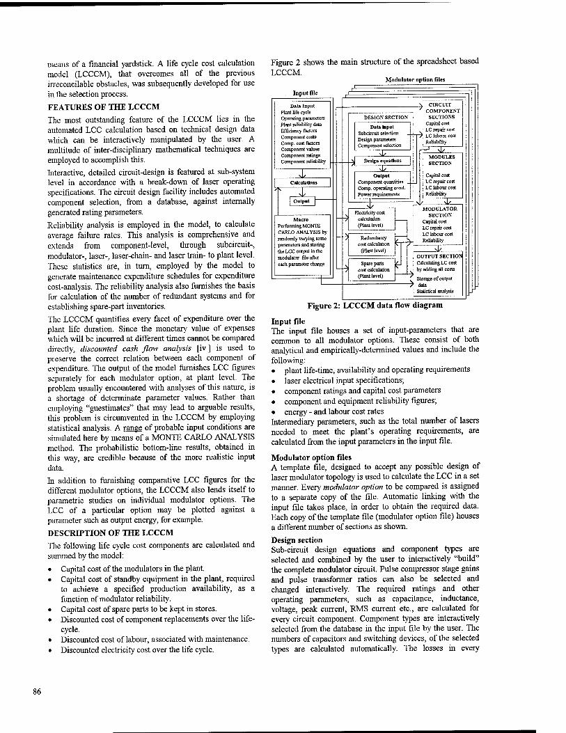
means of a financial yardstick. A life cycle cost calculation model (LCCCM), that overcomes all of the previous irreconcilable obstacles, was subsequently developed for use in the selection process.
FEATURES OF THE LCCCM
The most outstanding feature of the LCCCM lies in the automated LCC calculation based on technical design data which can be interactively manipulated by the user. A multitude of inter-disciplinary mathematical techniques are employed to accomplish this.
Interactive, detailed circuit-design is featured at sub-system level in accordance with a break-down of laser operating specifications. The circuit design facility includes automated component selection, from a database, against internally generated rating parameters.
Reliability analysis is employed in the model, to calculate average failure rates. This analysis is comprehensive and extends from component-level, through subcircuit-, modulator-, laser-, laser-chain- and laser train- to plant level. These statistics are, in turn, employed by the model to generate maintenance expenditure schedules for expenditure cost-analysis. The reliability analysis also furnishes the basis for calculation of the number of redundant systems and for establishing spare-part inventories.
The LCCCM quantifies every facet of expenditure over the plant life duration. Since the monetary value of expenses which will be incurred at different times cannot be compared directly, discounted cash flow analysis [iv] is used to preserve the correct relation between each component of expenditure. The output of the model furnishes LCC figures separately for each modulator option, at plant level. The problem usually encountered with analyses of this nature, is a shortage of determinate parameter values. Rather than employing "guestimates" that may lead to arguable results, this problem is circumvented in the LCCCM by employing statistical analysis. A range of probable input conditions are simulated here by means of a MONTE CARLO ANALYSIS method. The probabilistic bottom-line results, obtained in this way, are credible because of the more realistic input data.
In addition to furnishing comparative LCC figures for the different modulator options, the LCCCM also lends itself to parametric studies on individual modulator options. The LCC of a particular option may be plotted against a parameter such as output energy, for example.
DESCRIPTION OF THE LCCCM
The following life cycle cost components are calculated and summed by the model:
• Capital cost of the modulators in the plant. • Capital cost of standby equipment in the plant, required
to achieve a specified production availability, as a function of modulator reliability.
• Capital cost of spare parts to be kept in stores. • Discounted cost of component replacements over the life-
cycle. • Discounted cost of labour, associated with maintenance. • Discounted electricity cost over the life cycle.
Figure 2 shows the main structure of the spreadsheet based LCCCM.
Modulator option files
Input file
Data Input Plant life cycle Operating parameters Plant reliability data Efficiency factors Component costs Comp. cost factors Component values Component ratings Component reliability
JZ
JZ Output
Macro Performing MONTE CARLO ANALYSIS by randomly varying some parameters and storing the LCC output in the modulator file after each parameter change
DESIGN SECTION
Data input Subcircuit selection Design parameters Component selection
\i Design equations
3Z Output
Component quantities Comp. operating cond. Power requirements
3z Electricity cost
calculation (Plant level)
Redundancy cost calculation
(Plant level) <^
Spare parts cost calculation (Plant level) ft
\; CIRCUIT 7 COMPONENT
SECTIONS Capital cost LC repair cost LC labour cost Reliability
I3Z MODULES SECTION
Capital cost LC repair cost LC labour cost Reliability
3Z MODULATOR
SECTION Capital cost LC repair cost LC labour cost Reliability
3Z OUTPUT SECTION Calculating LC cost by adding all costs
Storage of output data Statistical analysis
Figure 2: LCCCM data flow diagram
Input file The input file houses a set of input-parameters that are common to all modulator options. These consist of both analytical and empirically-determined values and include the following: • plant life-time, availability and operating requirements • laser electrical input specifications; • component ratings and capital cost parameters • component and equipment reliability figures; • energy - and labour cost rates Intermediary parameters, such as the total number of lasers needed to meet the plant's operating requirements, are calculated from the input parameters in the input file.
Modulator option files A template file, designed to accept any possible design of laser modulator topology is used to calculate the LCC in a set manner. Every modulator option to be compared is assigned to a separate copy of the file. Automatic linking with the input file takes place, in order to obtain the required data. Each copy of the template file (modulator option file) houses a different number of sections as shown.
Design section Sub-circuit design equations and component types are selected and combined by the user to interactively "build" the complete modulator circuit. Pulse compressor stage gains and pulse transformer ratios can also be selected and changed interactively. The required ratings and other operating parameters, such as capacitance, inductance, voltage, peak current, RMS current etc., are calculated for every circuit component. Component types are interactively selected from the database in the input file by the user. The numbers of capacitors and switching devices, of the selected types are calculated automatically. The losses in every
86
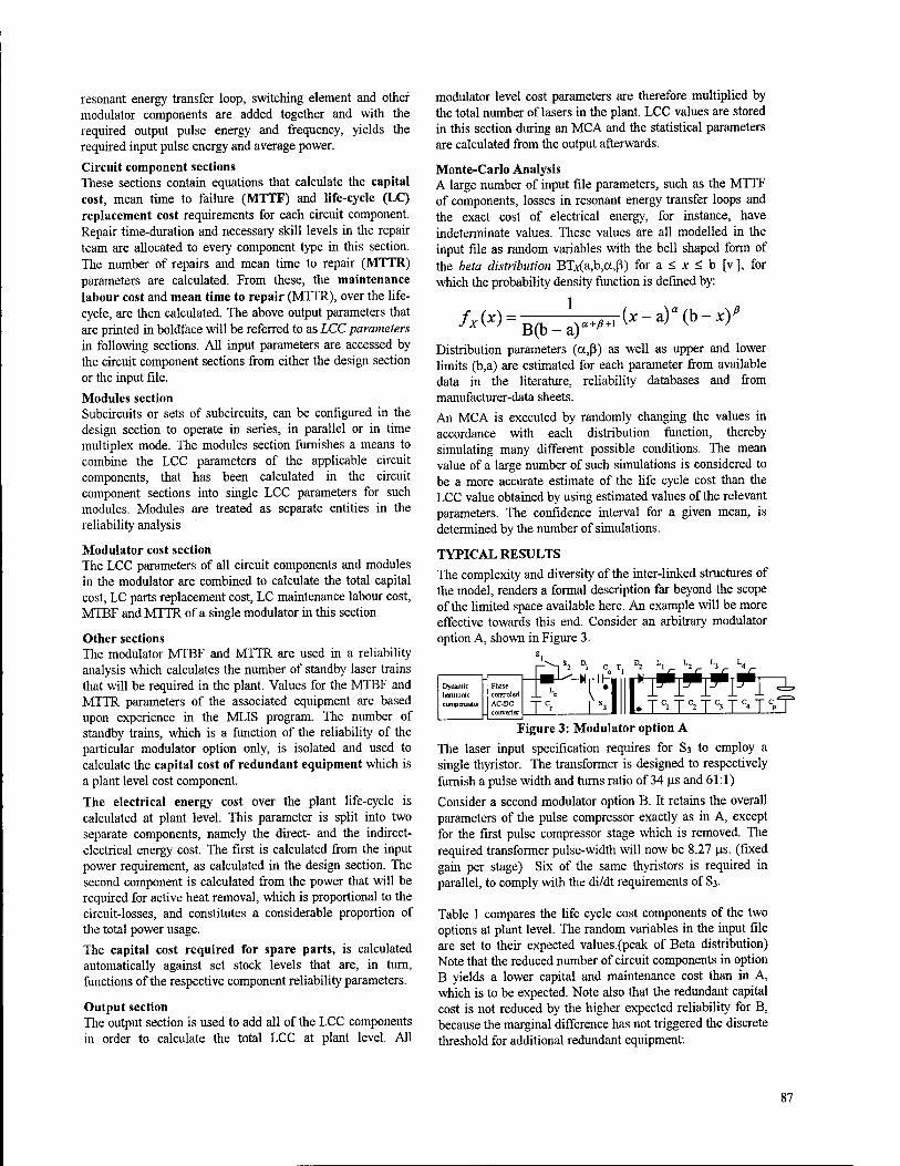
resonant energy transfer loop, switching element and other modulator components are added together and with the required output pulse energy and frequency, yields the required input pulse energy and average power.
Circuit component sections These sections contain equations that calculate the capital cost, mean time to failure (MTTF) and life-cycle (LC) replacement cost requirements for each circuit component. Repair time-duration and necessary skill levels in the repair team are allocated to every component type in this section. The number of repairs and mean time to repair (MTTR) parameters are calculated. From these, the maintenance labour cost and mean time to repair (MTTR), over the life- cycle, are then calculated. The above output parameters that are printed in boldface will be referred to as LCC parameters in following sections. All input parameters are accessed by the circuit component sections from either the design section or the input file.
Modules section Subcircuits or sets of subcircuits, can be configured in the design section to operate in series, in parallel or in time multiplex mode. The modules section furnishes a means to combine the LCC parameters of the applicable circuit components, that has been calculated in the circuit component sections into single LCC parameters for such modules. Modules are treated as separate entities in the reliability analysis
Modulator cost section The LCC parameters of all circuit components and modules in the modulator are combined to calculate the total capital cost, LC parts replacement cost, LC maintenance labour cost, MTBF and MTTR of a single modulator in this section
Other sections The modulator MTBF and MTTR are used in a reliability analysis which calculates the number of standby laser trains that will be required in the plant. Values for the MTBF and MTTR parameters of the associated equipment are based upon experience in the MLIS program. The number of standby trains, which is a function of the reliability of the particular modulator option only, is isolated and used to calculate the capital cost of redundant equipment which is a plant level cost component.
the electrical energy cost over the plant life-cycle is calculated at plant level. This parameter is split into two separate components, namely the direct- and the indirect- electrical energy cost. The first is calculated from the input power requirement, as calculated in the design section. The second component is calculated from the power that will be required for active heat removal, which is proportional to the circuit-losses, and constitutes a considerable proportion of the total power usage.
The capital cost required for spare parts, is calculated automatically against set stock levels that are, in turn, functions of the respective component reliability parameters.
Output section The output section is used to add all of the LCC components in order to calculate the total LCC at plant level. All
modulator level cost parameters are therefore multiplied by the total number of lasers in the plant. LCC values are stored in this section during an MCA and the statistical parameters are calculated from the output afterwards.
Monte-Carlo Analysis A large number of input file parameters, such as the MTTF of components, losses in resonant energy transfer loops and the exact cost of electrical energy, for instance, have indeterminate values. These values are all modelled in the input file as random variables with the bell shaped form of the beta distribution BTx(a,b,a,ß) for a < x < b [v ], for which the probability density function is defined by:
AM=B(b-lr'--(,-')'(l,-T)' Distribution parameters (a,ß) as well as upper and lower limits (b,a) are estimated for each parameter from available data in the literature, reliability databases and from manufacturer-data sheets.
An MCA is executed by randomly changing the values in accordance with each distribution function, thereby simulating many different possible conditions. The mean value of a large number of such simulations is considered to be a more accurate estimate of the life cycle cost than the LCC value obtained by using estimated values of the relevant parameters. The confidence interval for a given mean, is determined by the number of simulations.
TYPICAL RESULTS
The complexity and diversity of the inter-linked structures of the model, renders a formal description far beyond the scope of the limited space available here. An example will be more effective towards this end. Consider an arbitrary modulator option A, shown in Figure 3.
Figure 3: Modulator option A
The laser input specification requires for S3 to employ a single thyristor. The transformer is designed to respectively furnish a pulse width and turns ratio of 34 us and 61:1)
Consider a second modulator option B. It retains the overall parameters of the pulse compressor exactly as in A, except for the first pulse compressor stage which is removed. The required transformer pulse-width will now be 8.27 us. (fixed gain per stage) Six of the same thyristors is required in parallel, to comply with the di/dt requirements of S3.
Table 1 compares the life cycle cost components of the two options at plant level. The random variables in the input file are set to their expected values.(peak of Beta distribution) Note that the reduced number of circuit components in option B yields a lower capital and maintenance cost than in A, which is to be expected. Note also that the redundant capital cost is not reduced by the higher expected reliability for B, because the marginal difference has not triggered the discrete threshold for additional redundant equipment.
87

Option
Costs A B
Capital (active equip) M$ 9.84 8.16
Capital (redundant) MS 2.52 2.52
Capital (Spare parts) MS 0.27 0.24
Parts replacement MS 3.72 3.28
Maintenance labour MS 0.32 0.38
Direct electrical energy MS 6.31 5.88
Indirect electrical energy MS 0.95 0.82
Total LCC MS 24.19 21.28
Table 1: LCC components
The electrical energy cost required for B is lower than that of A due to the higher efficiency that the reduced number of resonant energy transfer loops brings about.
It is important to observe that the capital cost constitutes only a moderate fraction of the total LCC in both cases as shown in a breakdown of the LCC of option A in Figure 4.
multiplexing. • Higher DC input voltages to the charging circuit
generally reduces LCC. • Systems employing ramp- capacitor charging circuits
have lower LCC than those with resonant charging circuits.
Although these rules were established with this model, which is tailored to this specific application, they appear to be generally applicable. Designers are advised, however, to carry out their own analysis of this type for any new commercial application.
VI
200
INDIRECT ELECTRICITY
Life cycle cost [MS]
Figure 5: MCA output of option A
COMPONENT REPLACEMENT
COST 15%
SPARE PART CAPITAL COST
REDUNDANT EQUIPMENT COST
10%
Figure 4: Cost components of option A
Figures 5 and 6 respectively show the frequency distributions of MCA outputs of 500 simulations each for both options.
Option
Parameter A B
Sample std. deviation M$ 3.33 3.03
95% confidence interval MS + 0.29 ±0.27
Sample mean LCC MS 25.75 22.53
Table 2: Statistical output parameters
Table 2 compares the calculated statistical output parameters for A and B. Obviously, B is preferable to A in this instance.
CONCLUSIONS
The LCCCM is currently used to compare various modulator options against each other for the envisaged plant. The following general rules, for decreasing life cycle cost, has been observed to date :
• The use of small sub-circuit modules in stead of higher rated single sub-circuits, to achieve higher peak power values are more expensive to use.
• If the use of sub-circuit modules or multiple components are mandatory, to achieve a given requirement, parallel connection of subsystems or devices are preferred above
zuu -
150 -
100 - 1 50 -
I i i-i'ri li o J 'PIMI'I-H 11 ii 11111111 V© © 00
Life cycle cost [MS]
Figure 6: MCA output of option B
REFERENCES [i ]Levy S, et. al., "COMMERCIAL APPLICATIONS FOR MODULATORS AND PULSE POWER TECHNOLOGY", Conference Record of the 1992 20th Power Modulator Symposium, June 23-25, 1992, Myrtle Beach, South Carolina, p8
[ii JRabinowitz P, Stein A, Kaldor A, Infrared multiphoton dissociation of UFg, Optical Communication, vol. 27,1982
[iii ] Arsenault JE, Roberts JA, Reliability and Maintainability of Electronic Systems, COMPUTER SCIENCE PRESS, Maryland, 1980.
[iv] Horngren CT, Foster G, COST ACCOUNTING, A MANEGERIAL EMPHASIS, 6th edition, Prentice-Hall International, New Jersey, 1987
[vJBenjamin JR, Cornell CA, Probability. Statistics and Decision for Civil Engineers, McGraw-Hill, New York, 1970.
CATHODIC ARC MODULATOR SYSTEMS FOR METALLIC PLASMA ION IMPLANTATION
by W.A. RE ASS and B.P. WOOD
LOS ALAMOS NATIONAL LAB PO BOX 1663, LOS ALAMOS NM 87545
(505) 665-1013
ABSTRACT
This paper describes the electrical design and operation of a cathodic arc modulator system for metallic plasma ion implantation. Depending on the ion implantation process recipe, various repetition rates, pulse widths, and currents are required. In addition, the cathodic arc system may be synchronized with a higher voltage "target" modulator system. The cathodic arc is water cooled and usually uses a self generated axial B-field, by use of a series connected solenoid around the arc anode. Typical arc currents of 800 amperes may be utilized with pulse widths ranging from 20 uS to 4 mS. Typical PRF's may exceed 400 Hz, with overall system power limited by our presently available 10 kW transformer- rectifier. The cathodic arc modulator system consists of a command charged 10 kV trigger generator, a high voltage arc "starter", and a low voltage, high current arc sustain circuit. The arc start and sustain circuits are independently adjustable and utilize a common IGBT device in a "hot-deck" configuration. This paper will provide circuit design and performance information in addition to various process applications.
MODULATOR DESIGN
To synchronize the arc with a target implant modulator, reliable and predictable triggering and arc sustainment are required. The arc voltage will vary as compared to a true vacuum metallic arc (30 to 50 V) due to
magnetic field and possible additional plasma background process gasses. A recipe step may or may not use additional background plasma gases, such as oxygen, to implant metallic oxides (ceramics). Depending on process recipe, various axial field coils may also be used, smaller coils (lower inductance) may be used for short pulse application for metallic interface layer implants. Independently adjustable high- voltage arc start and low-voltage arc sustain circuits are used as shown in Figure 1 for operational flexibility. Figure 2 is a diagrammatic representation of the cathodic arc. The arc sequence is initiated by switching the IGBT hot deck. In a few microseconds, depending on the axial field coil, the anode-cathode arc gap is charged to the arc start voltage (-500 V). The arc is triggered and the discharge limited to -100 amperes by the start circuit swamping resistor. After a few tens of microseconds, the isolating diode is forward biased and the low voltage arc sustain circuit provides the remaining pulse energy. A low resistance in the IGBT hot deck limits the current switched by the arc sustain circuit. A high voltage arc system would trigger reliably, but be inefficient in operation. A low voltage arc system is difficult to trigger reliably and with little jitter. This simple design has proved reliable and flexible with machine operations with typical voltage and current waveforms as shown in Figures 3 and 4. A photo of a filtered carbon cathodic arc for diamond deposition is shown in Figure 5.
0-7803-3076-5/96/S5.00 © 1996 IEEE 89
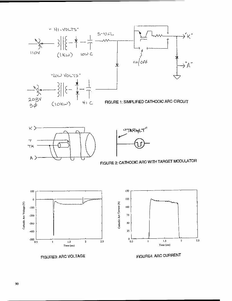
\\o\J
ys.
5^
^ )-)| -VDL.TV
T
5>~>0-O_.
(UuO louJC
"Lou> VoUTS'
ODW) ^'C
L-yAA-
X
*V
->A
X7
FIGURE 1: SIMPLIFIED CATHODIC ARC CIRCUIT
TK
O VJ FIGURE 2: CATHODIC ARC WITH TARGET MODULATOR
>
1UU
0
1 1 1
^——J^ -100 -
-200 • •
-300 ■ ■
-400 • -
0.5 1 1.5 2
Time (ms)
FIGURE3: ARC VOLTAGE
2.5
t u
•s
ÜU
125
100 1 75
50 •
25
. J I 0.5 1.5
Time (ms)
FIGURE4: ARC CURRENT
2.5
90
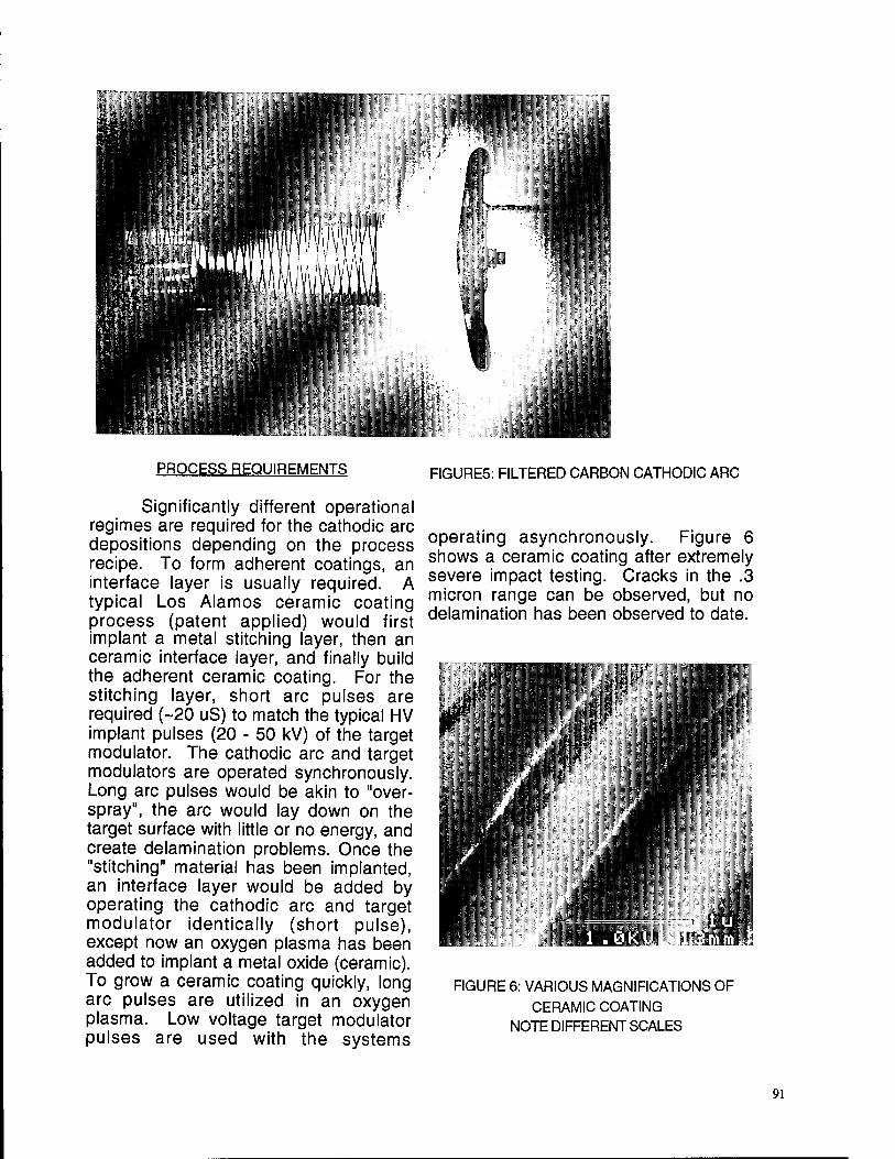
fiH
litt!
Mi I If Hii
W lllill
11-illKi
III 111
rltiwilHiliE IllfltlllPt 1IIJöHKI 1 B'i
PROCESS REQUIREMENTS
Significantly different operational regimes are required for the cathodic arc depositions depending on the process recipe. To form adherent coatings, an interface layer is usually required. A typical Los Alamos ceramic coating process (patent applied) would first implant a metal stitching layer, then an ceramic interface layer, and finally build the adherent ceramic coating. For the stitching layer, short arc pulses are required (-20 uS) to match the typical HV implant pulses (20 - 50 kV) of the target modulator. The cathodic arc and target modulators are operated synchronously. Long arc pulses would be akin to "over- spray", the arc would lay down on the target surface with little or no energy, and create delamination problems. Once the "stitching" material has been implanted, an interface layer would be added by operating the cathodic arc and target modulator identically (short pulse), except now an oxygen plasma has been added to implant a metal oxide (ceramic). To grow a ceramic coating quickly, long arc pulses are utilized in an oxygen plasma. Low voltage target modulator pulses are used with the systems
FIGURE5: FILTERED CARBON CATHODIC ARC
operating asynchronously. Figure 6 shows a ceramic coating after extremely severe impact testing. Cracks in the .3 micron range can be observed, but no delamination has been observed to date.
i 1 1 ■ jBSftt -■■■■ ■: ! :,,,'' > '■• ']: ■ At
Ä ?•;,- '■"'.■'-";ir ::- ifjpi
FIGURE 6: VARIOUS MAGNIFICATIONS OF CERAMIC COATING
NOTE DIFFERENT SCALES
91

i"■*-• ■ * Aravy;„■"■ , ■ Wi'lÄ LM fl45 raroVtwi CW
■n 7"
<IifT2£lXt ET**-.
fen> '"*%, V*MS Wfe?'' 3 41M'1- v;,i r v "'; W'yiL,
;-•; !^>-:W' W
FIGURE 6: VARIOUS MAGNIFICATIONS OF CERAMIC COATING NOTE DIFFERENT SCALES
CONCLUSION
Plasma processing is a modulator intensive technology. Many new applications and recipes are being developed to meet many military, consumer, and industrial applications. Modulator techniques for cathodic arc processing are simple and could be easily assimilated by industry once process recipe and material performances are determined. Los Alamos will continue to work with industrial and military researchers to identify and develop environmentally consious and advanced material process techniques.
92
PROGRESS TOWARDS A 20 KV, 2 KA PLASMA SOURCE ION IMPLANTATION MODULATOR FOR AUTOMOTIVE PRODUCTION OF DIAMOND FILM ON ALUMINUM
by W.A. Reass and C.A. Munson
Los Alamos National Lab P.O. Box 1663, Los Alamos, NM 87545
(505) 665-1013 and
Gerard Malaczynski and Alaa Elmoursi General Motors Research Laboratory
30500 Mound Rd., Warren, Ml 48090 (810) 986-0348
INTRODUCTION This paper provides the process
requirements and the electrical design topology being developed to facilitate large scale production of amorphous diamond films on aluminum. The patented recipe, that includes other surface modification processes, requires various operational voltages, duty cycles, and current load regimes to ensure a high quality film.. It is desirable to utilize a common modulator design for this relatively "low voltage" recipe. Processing may include target part cleaning, ion implantation, plasma deposition, and vacuum chamber cleaning. Modulator performance will have a direct impact on plant size and system economics. Unfortunately, process requirements are in a regime that is not easily achievable by solid state or very efficiently by vacuum tube devices.
To accommodate the various process requirements, we are developing a modulator based on series connected hot decks utilizing high current, high voltage IGBT devices. Although some manufacturers have released 2500 volt devices, we have chosen the 400 ampere, 1700 volt devices, for this first development, because of their superior switching performance. To protect the IGBT's from voltage transients, in addition to the typical (internal) back swing and output freewheel diodes, individual IGBT varistors and snubbers are utilized in combination with an output fault limiting resistor. Power to each hotdeck is provided by a low capacitance isolation transformer with I/O via fiber optics. To ensure appropriate IGBT gate control, a tailored 50 amp driver with a complementary outputs is utilized. To ensure IGBT safety margin and minimize system ringing, a series output resistor limits hard faults two twice the IGBT's continuos rating. The intent is to ensure reliability of the switching system, regardless if the protect system fails.
Adjustments in system voltage are accommodated by phase control of the transformer-rectifier. For vacuum chamber cleaning, polarity reversing switch are required.
A review of the system requirements and design approach will be presented in addition to test results.
SYSTEM CONFIGURATION
To rapidly commercialize this plasma processing procedure, maximum use of utility and commercial equipment will be utilized, as shown in Figure 1. A reverse connected 30 utility transformer will provide the 20 kV for the implant procedure. A phase controller will provide adjustment in process voltage. For low voltage deposition (few kV) a tap changer may be required to maintain a good power factor (not presently included). A flexible system may be configured as shown in Figure 2. A switch box , in combination with internal modulator polarity switches, can be used to clean the process vacuum chamber with it's associated cleaning electrode. A high voltage step-up transformer may also be used for the typical 100 kV nitrogen implant process. Figure 3 shows the simplified block diagram of the IGBT hot deck with polarity reversing switches. This first Los Alamos construction will not use reversing switches, cables will be manually changed to reverse polarity.
IGBT SERIES SWITCH DECKS
Twenty series connected hotdecks are connected as shown in Figure 4. Power to the individual hotdecks is provided by low capacitance windings wound on a common core. To limit and equalize transient and static IGBT voltages, each hot deck has a low inductance RC snubber and varistor. Leakage current is absorbed by an output "pull-down" resistor (not shown on Fig. 4). The pulldown resistor is chosen to limit the plasma inter-pulse voltage to -50 v to prevent sputtering and deposition. Although one may not absolutely require RC snubbers, the author believes they may be beneficial as varistors can have poor time response characteristics (10-100 nS) in the regime
0-7803-3076-5/96/S5.00 © 1996 IEEE 93
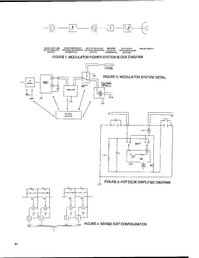
i a—v
—VA—1(-
13.8 kV to 480 V (30) PHASE CONTROLLER 480 V TO 13.8 KV (30) RECTIFIER SOLID STATE INPLANT OBJECT UTILITY LINE INPUT (VOLTAGE ADJUSTMENT) (REVERSE CONNECTED) (AC TO DC) PULSE MODULATOR
(UTILITY) (COMMERCIAL) (UTILITY) (COMMERCIAL) (CUSTOM)
FIGURE 1: MODULATOR POWER SYSTEM BLOCK DIAGRAM
->—c 8Äfe
FIGURE 2: MODULATOR SYSTEM DETAIL
-W—
-AA/\ |fc-
~v/~
Jy -a-
rh FIGURE 3: HOT DECK SIMPLIFIED DIAGRAM
—»fc- —VA—l(r
-w- /
-^Vv
-AAA |£-
-KJ- /
FIGURE 4: SERIES IGBT CONFIGURATION
94
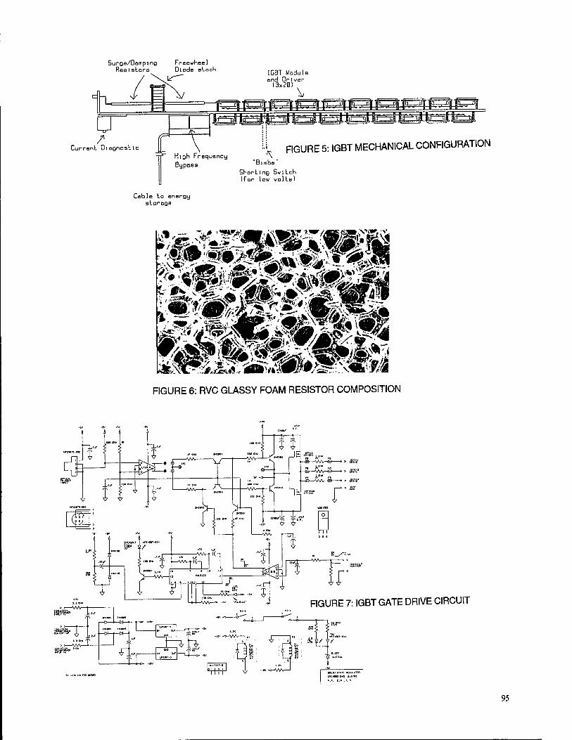
Surge/DamplnQ Freewheel Resistors Diode stock IGBT Module
ond Driver 13x20)
Current Diagnostic
High Frequency Bypass *Blmbn
FIGURE 5: IGBT MECHANICAL CONFIGURATION
Shorting Switch (for low volts)
Coble to energy storage
FIGURE 6: RVC GLASSY FOAM RESISTOR COMPOSITION
FIGURE 7: IGBT GATE DRIVE CIRCUIT
I/1V IN.EM «J1HJ
95
that may cause IGBT's to latch or over-volt. Computer modeling has shown transient loads and inherent differences in device and driver time delays can cause device over-voltage (and failure). All protection methods may be necessary to prevent IGBT device failure. To limit transient voltage and fault current during the frequent plasma arc-downs, output resistance is required to limit varistor excursions and protect the IGBT's. Large diameter varistors have a lower AC impedance and a more effective clamp voltage, but limits in varistor dynamic range are still required. A 20 series stack gives a 34 kV voltage compliance, with each deck having 3 parallel devices, a 1200 ampere continuous rating is obtained. The mechanical configuration will be implemented as shown in Figure 5. The IGBT hot decks form a parallel plate transmission line on each side of the ground return buss.
SNUBBER AND SERIES DAMPING RESISTORS
To help protect each transistor from voltage transients, low inductance snubbers will be used. Additionally, at high rep-rates, high power dissipation is also required (-400W at 2 kHz). We are developing two styles of water cooled IGBT snubber resistor. A new material "Reticulated Vitreous Carbon" (RVC) shows extreme promise. RVC is a glassy carbon available with various porosity, ligament diameter, and density. Resistivity can be chosen to optimize a design. The range of resistivities fall between that of "granular" carbons (as used in glo-bar or disc devices) and metals. Los Alamos has tested these devices to 15 kA/cm2, 850 kA, and 130 J/cc. The resistance is not affected by oil or water and should be capable of "infinite" power dissipation due to "infinite" surface area. The glassy RVC is continuos from end to end and does not suffer from grain boundary problems as typical organic and ceramic carbon resistors. We are also examining the use of stainless steel gauze as a resistor element in the snubber networks. Our only consideration for an output fault limiting resistor at this time are RVC elements. Figure 6 shows the composition of the RVC material.
IGBT GATE DRIVE
Los Alamos has developed and tested a number of IGBT gate drive circuits. The author felt currently available gate drive modules have insufficient drive current for parallel networks of large IGBT devices. Any design must be cognizant of thermally induced timing drift and delay. Saturated switching circuits can be very sensitive with temperature due to storage delay effects. Circuit modeling shows over-voltage conditions (without protection) with differences as little as 25 nS in a series stack. We have also slowed down our 50 amp output gate drive switching speeds, to 120 nS Tr & Tf, to reduce the probability of IGBT latch-up and reduce turn-off transients. We found excessively fast IGBT gate fall times (in excess of IGBT "Ic" fall) can induce latch-up in some manufacturers devices. The gate drive board mounts directly to the IGBT's to minimze wiring inductance and improve reliability. The schematic is shown in Figure 7, and is capable of driving three IGBT's. The fast over-voltage protect will not be utilized "on board ".
CONCLUSION
The system as described is presently being fabricated and will assume operational capabilities in early 1997. Many additional sub- systems such as polarity reversal and chamber cleaning process procedures will then be able to be further evaluated. For the amorphous diamond process to be successful, the automotive industry will require very reliable modulator systems that can be maintained by the average electronics technician. We believe this first effort is capable of meeting these goals.
96
DEVELOPMENT LEADING TO A 200 KV, 20 KA, 30 HERTZ RADAR-LIKE MODULATOR SYSTEM FOR INTENSE ION BEAM PROCESSING
by W. Reass, H. Davis, and J. Olson
Los Alamos National Lab P.O. Box 1663 Los Alamos NM 87545
and D. Coates and H. Schleinitz
DuPont Central Research and Development P.O. Box 80356 Wilmington, DE 19880
INTRODUCTION
This paper presents the electrical system design methodology we are developing for use in the Los Alamos "CHAMP" (Continuous High- Average Power Microsecond Pulser) program. CHAMP is a Magnetically confined Anode Plasma diode (MAP diode) intense ion source. The CHAMP diode ion source requires many synchronous modulator sub-systems slaved to that required by the diode discharge itself (200 kV, 20 kA). At common potential with the pulsed anode, a gas puff modulator and fast gas pre- ionization modulator sub-system are fabricated in a "hotdeck" chassis. Fiber optic cables provide the appropriate fast control and diagnostic I/O. A pair of Hemholtz-like field coils, surrounding the anode-cathode gap, provides an insulating field that prevents electrons from closing the anode- cathode gap. These field coils are also synchronized to the MAP diode and will utilize energy recovery techniques in it's final form. A dedicated fast sequence and monitor system ensure the proper sub-system parameters before the main diode discharge is initiated. The main diode modulator system will utilize 4 parallel type "E" Blumlein lines each switched with a CX1736AX thyratron. This tube is a 4.5" diameter, 70 kV, two gap, hollow anode device. The four parallel networks will drive a 3.33:1 transformer of Los Alamos design. A bifilar wound secondary provides power to the gas modulator system hotdeck. Although the complete system will not be operational for another year, computer modeling suggests we should easily be able to generate 1 uS pulses with a 300 nS rise and fall. The MAP diode is not particularly sensitive to pulse fidelity, which eases network design. A realizable system could use half-sine pulses, but at a sacrifice to peak ion energy distribution.
In addition to overall CHAMP diode system requirements, the design of the pertinent electrical pulse modulator systems will be presented.
MAP DIODE CONFIGURATION
A diagrammatic view of the MAP diode is shown in Figure 1. Key sub-systems include a gas puff valve and modulator, a plasma induction coil and modulator, and an insulation field coil and modulator system. These systems require proper sequential operation to achieve the desired ion beam energy, focus, and fluence. Once these systems have achieved their proper parameters, the ion beam can be initiated by discharging the Blumlein line PFN. Any improper sequence or anomaly, if not properly detected, can lead to high PFN reversals and deleterious thyratron waveforms. The insulating field coils require about 100 uS to reach peak current and are the first system to energize. This field provides long field lines in the anode-cathode gap and prevent electrons from shorting out the gap during the ion beam discharge. The gas puff modulator, operating at the anode pulse potential, initiates a gas puff from a circular plenum that is sealed by a washer (and o-rings). A flat pancake coil behind the washer operates with a 10 uS quarter period to reactively open the plenum. An acceleration nozzle then expands the gas out into the induction coil region. The induction coil modulator performs two functions, first to break down the gas and then to push the plasma out against the insulation field. The proper induction coil current will have the plasma stagnate in the map diode pole faces to await ion beam extraction during the PFN pulse. The main discharge of the induction coil circuit operates with a 1 uS quarter period. The Blumlein line as designed (and modeled) has a rather trapezoidal waveform that will deposit ion energy over a greater range of target depth that is better suited for some material process applications. An engineering advantage of this system is that pulse fidelity is not strongly dependent on pulse transformer leakage inductance. This PFN system will probably never see a well matched load during operation and will necessitate the use of hollow anode thyratrons. The MAP diode should present about a 16 Ohm load around 220 kV. The system block diagram is shown in Figure 2. The induction coil and puff
0-7803-3076-5/96/S5.00 © 1996 IEEE 97
High Vottage
200 - 250 kV 15 0hm 1 |IS
FIGURE 1: VIEW OF "MAP" DIODE
Diode
- CX1736 AX One ot 4 parallel networks 70KV,15kA
1 "iV (AC Power Input)
FIGURE 2: SIMPLIFIED BLOCK DIAGRAM OF CHAMP SYSTEM
I h B-i
Magnet Coll Modulator
'energy recovery
98
^Mauhnw****
*~2
tÄ, FIGURE 3: SIMPLIFIED GAS PUFF MODULATOR no**
5 o laOPF 30hV
+V »-wv "—&■
Hf- 4a I.B OWl
|^WV-|
-JWV-
^V ^ ^ ODP—• •
-€1
-% <y
J3- l/Wifi.dl g
I27Y-2T2533
TRIGGER (J.7.B
3.4.5
T
DP MB
l5-£
CA-i-T .HIV/A
e}—&—
a
-7toaH 3-r
as*
FIGURE 4: SIMPLIFIED INDUCTION COIL MODULATOR
Gate Valve
Pulse Processing
Module &Oil Tank ^^ Sample
y \ Module
Vacuum Pump
13'Long
(8' Wide)
FIGURE 5: CHAMP SYSTEM LAYOUT
99
valve modulators are located in a hot deck and powered by the pulse transformer's bifilar winding. Fast fiber optic I/O ensure proper triggering and operational parameters. The insulating field coil modulator will eventually require energy recovery techniques to minimize coil power dissipation at 30 Hz, about 30 kW without energy recovery. Initial system operation will be at 5 Hz and below. The Blumlein lines are designed with our existing paper capacitors, rated for 100 kV. A significant engineering disadvantage of the Blumlein line is the 100% voltage reversal on the lower PFN capacitors. Mica capacitors may be better suited for this application.
GAS PUFF AND INDUCTION COIL MODULATORS
The gas puff modulator is relatively simple and is shown in Figure 3, a capacitor and SCR discharge circuit. The gas puff valve requires about a 7 kA pulse. Unfortunately at this time, the puff valve has mechanical design limitations above 5 Hz. Another technology may be required for eventual 30 Hz operation. The induction coil driver delivers an 8 MHz waveform superimposed on a 1 uS quarter period waveform. The circuit topology in Figure 4 shows a two loop circuit connected to the coils. When the spark gap is triggered, the load coils ring with the array of 100 pf capacitors. The coil voltage must ring through zero to initiate good gas breakdown. The voltage reversal is facilitated by the saturable reactor holding off the high current (20 kA) discharge from the second loop for a few tens of nS.
SYSTEM LAYOUT
The system layout is shown in Figure 5. The overall CHAMP modulator and process chamber require a small footprint, 8' X 13' X 7' high. The PFN will be in a low inductance configuration, the capacitor bushings down and the inductors near the return plane, at the bottom of the oil tank. The thyratrons will be partially enclosed in re- entrant metal cans extending below the return plane. Low inductance output bus will connect to the pulse transformer. The hotdeck is located above the PFN capacitors. A more optimal design would use the available shorter capacitors to lower the hotdeck assembly. The vacuum and process chambers are placed on roller tracks to permit their separation and maintenance.
CONCLUSION
The push to commercialize the CHAMP system is very strong. Their are many exciting and promising ion beam processes that are being patented for large scale consumer application. To achieve required rep-rates and system reliability, for high process production, iterations in component technologies and sub-system designs will be required. Equipment must also be designed that can be easily maintained or repaired by the manufacturers technicians that won't necessarily be pulse modulator specialists. Los Alamos looks forward to working with equipment manufacturers to help facilitate these important goals.
100
AN INDUSTRIAL APPLICATION OF A PULSED POWER MODULATOR
H. Anamkath, F. Gower, R. Mendonsa, R. Miller, K. Whitham, A. Zante
Titan Beta, 6780 Sierra Court, Dublin, CA 84568
Introduction
Titan Beta has designed and manufactured a 12 MW, 100 kW modulator as part of Titan's 10 MeV, 15 kW Linear Accelerator (Linac) electron beam industrial processing system. These systems are designed to operate at a duty of 7000 hours or greater per year. Two of the three Linac systems produced by Titan Beta are operated by the Titan Corporation. Titan integrates the Linac systems into their turn key medical product sterilization facilities and provides the material handling, shielding and all necessary controls and documentation required to conform to FDA requirements for the sterilization of medical products.
The first Linac system was delivered in July of 1993 to Titan Scan's facility located in Denver, Colorado and is currently operating at its maximum capacity.
The second system began processing medical products at Titan's San Diego, California facility on January 1996 and is now ramping up to full production. The third Linac system was delivered to BSE Mediscan G.M.B.H. located in Kremsmünster, Austria and is being integrated into a medical sterilization facility. The Linac system, is presently undergoing final commissioning and integration.
Modulator History
Titan Beta has manufactured a wide range of high power RF sources for many applications. However, few have been specifically designed
and fabricated to operate reliably in excess of 7000 hours per year. That amounts to operating 24 hours per day for over 290 days per year. Yet this is the typical duty for Titan's industrial E-beam processing facilities for medical products.
June of 1993 marked the installation of Titan Beta's first commercially designed Linac for the exclusive use of the sterilization of new medical products at its contract facility located in Denver Colorado. The modulator was designed for a 10 MeV, 10 kW RF Linac and is operating successfully since the installation.
Titan commissioned a second sterilization facility in San Diego, California that went into production in January of 1996. The facility incorporates Titan Beta Model TB-10/15 RF Linac designed for 10 MeV, 15 kW output. The unit has been operating successfully since it was commissioned and is in the ramp up mode.
A sterilization facility has been built by BSE Mediscan at Kremsmünster, Austria. This facility incorporates a Titan Beta Model TB- 10/15 RF Linac designed for 10 MeV, 15 kW output. At present the Linac is undergoing final test and integration and the facility is scheduled to go on line production in late July 1996.
Modulator Description
The basic modulator design utilizes a type E Pulse Forming Network (PFN) with up to 16
0-7803-3076-5/96/S5.00 © 1996 IEEE 101
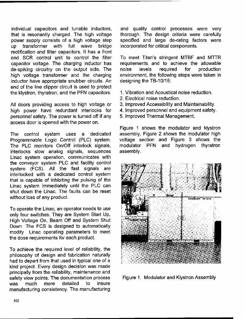
individual capacitors and tunable inductors, that is resonantly charged. The high voltage power supply consists of a high voltage step up transformer with full wave bridge rectification and filter capacitors. It has a front end SCR control unit to control the filter capacitor voltage. The charging inductor has de-spiking circuitry on the output side. The high voltage transformer and the charging inductor have appropriate snubber circuits. An end of the line clipper circuit is used to protect the klystron, thyratron, and the PFN capacitors.
All doors providing access to high voltage or high power have redundant interlocks for personnel safety. The power is turned off if any access door is opened with the power on.
The control system uses a dedicated Programmable Logic Control (PLC) system. The PLC monitors On/Off interlock signals, interlocks slow analog signals, sequences Linac system operation, communicates with the conveyor system PLC and facility control system (FCS). All the fast signals are interlocked with a dedicated control system that is capable of inhibiting the pulsing of the Linac system immediately until the PLC can shut down the Linac. The faults can be reset without loss of any product.
To operate the Linac, an operator needs to use only four switches. They are System Start Up, High Voltage On, Beam Off and System Shut Down. The FCS is designed to automatically modify Linac operating parameters to meet the dose requirements for each product.
To achieve the required level of reliability, the philosophy of design and fabrication naturally had to depart from that used in typical one of a kind project. Every design decision was made principally from the reliability, maintenance and safety view points. The documentation process was much more detailed to insure manufacturing consistency. The manufacturing
and quality control processes were very thorough. The design criteria were carefully specified and large de-rating factors were incorporated for critical components.
To meet Titan's stringent MTBF and MTTR requirements and to achieve the allowable noise levels required for production environment, the following steps were taken in designing the TB-10/15:
1. Vibration and Acoustical noise reduction. 2. Electrical noise reduction. 3. Improved Accessibility and Maintainability. 4. Improved personnel and equipment safety. 5. Improved Thermal Management.
Figure 1 shows the modulator and klystron assembly, Figure 2 shows the modulator high voltage section and Figure 3 shows the modulator PFN and hydrogen thyratron assembly.
Figure 1. Modulator and Klystron Assembly
102
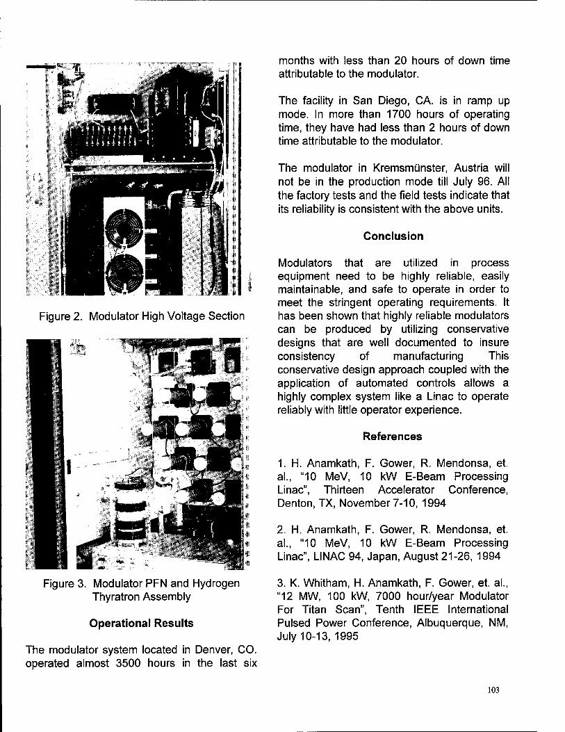
Figure 2. Modulator High Voltage Section
B" 'UM mW
Figure 3. Modulator PFN and Hydrogen Thyratron Assembly
Operational Results
The modulator system located in Denver, CO. operated almost 3500 hours in the last six
months with less than 20 hours of down time attributable to the modulator.
The facility in San Diego, CA. is in ramp up mode. In more than 1700 hours of operating time, they have had less than 2 hours of down time attributable to the modulator.
The modulator in Kremsmünster, Austria will not be in the production mode till July 96. All the factory tests and the field tests indicate that its reliability is consistent with the above units.
Conclusion
Modulators that are utilized in process equipment need to be highly reliable, easily maintainable, and safe to operate in order to meet the stringent operating requirements. It has been shown that highly reliable modulators can be produced by utilizing conservative designs that are well documented to insure consistency of manufacturing This conservative design approach coupled with the application of automated controls allows a highly complex system like a Linac to operate reliably with little operator experience.
References
1. H. Anamkath, F. Gower, R. Mendonsa, et. al., "10 MeV, 10 kW E-Beam Processing Linac", Thirteen Accelerator Conference, Denton, TX, November 7-10, 1994
2. H. Anamkath, F. Gower, R. Mendonsa, et. al., "10 MeV, 10 kW E-Beam Processing Linac", LINAC 94, Japan, August 21-26, 1994
3. K. Whitham, H. Anamkath, F. Gower, et. al., "12 MW, 100 kW, 7000 hour/year Modulator For Titan Scan", Tenth IEEE International Pulsed Power Conference, Albuquerque, NM, July 10-13, 1995
103
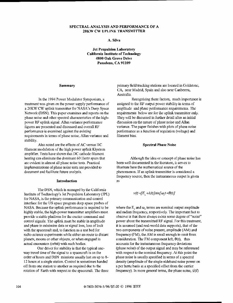
SPECTRAL ANALYSIS AND PERFORMANCE OF A 20KW CW UPLINK TRANSMITTER
A. Silva
Jet Propulsion Laboratory California Institute of Technology
4800 Oak Grove Drive Pasadena, CA 91109
Summary
In the 1994 Power Modulator Symposium, a treatment was given on the power supply performance of a 20KW CW uplink transmitter for NASA's Deep Space Network (DSN). This paper examines and reports on the phase noise and other spectral characteristics of the high- power RF uplink signal. Allan variance performance figures are presented and discussed and overall RF performance is examined against the existing requirements in terms of phase noise, Allan variance and stability.
Also noted are the effects of AC versus DC filament modulation of the high power uplink Klystron amplifier. Tests have shown that DC cathode filament heating can eliminate the dominant 60 Hertz spurs that are evident in almost all phase noise tests. Practical implementations of phase noise tests are provided to document and facilitate future analysis.
Introduction
primary field tracking stations are located in Goldstone, CA, near Madrid, Spain and also near Canberrra, Australia.
Recognizing these factors, much importance is assigned to the RF output power stability in terms of amplitude and phase performance requirements. The requirements below are for the uplink transmitter only. They will be discussed in further detail after an initial discussion on the nature of phase noise and Allan variance. The paper finishes with plots of phase noise performance as a function of regulation (voltage) and filament bias.
Spectral Phase Noise
Although the idea or concept of phase noise has been well documented in the literature, it serves to illustrate here the mathematical source of the phenomenon. If an uplink transmitter is considered a frequency source, then the instantaneous output is given as
The DSN, which is managed by the California Institute of Technology's Jet Propulsion Laboratory (JPL) for NASA, is the primary communication and control interface for the US space program deep space probes of NASA. Because the uplink performance is required to be highly stable, the high-power transmitter amplifiers must provide a stable platform for the exciter command and control signals. The uplink must be stable in amplitude and phase to minimize data or signal loss, loss of lock with the spacecraft and, to function as a test bed for radio-science experiments while either en-route to distant planets, moons or other objects, or when engaged in actual encounters (orbit) with such bodies.
One driver for stability is that the typical one- way travel time of the signal to a spacecraft is on the order of hours and DSN missions usually last on up to 8- 12 hours at a single station. Control is sometimes handed off from one station to another as required due to the rotation of Earth with respect to the spacecraft. The three
v(t)=[E+A(t)]sin[a>t+6(t)]
where the Ec and coc terms are nominal output amplitude and radian frequency, respectively. The important fact to observe is that there always exists some degree of "noise" power about the transmitted RF signal. For this treatment, it is assumed (and real-world data supports), that of the two components of noise present, amplitude (AM) and frequency (FM), the AM is small enough to omit from consideration. The FM component left, 0(t), thus accounts for the instantaneous frequency deviations (phase noise) of the output signal and may be referenced with respect to the nominal frequency. At this point the phase noise is usually specified in terms of a spectral density (amplitude of the single-sideband noise power on a per hertz basis at a specified offset from the carrier frequency). In more general terms, the phase noise, S£(f)
104 0-7803-3076-5/96/S5.00 © 1996 IEEE
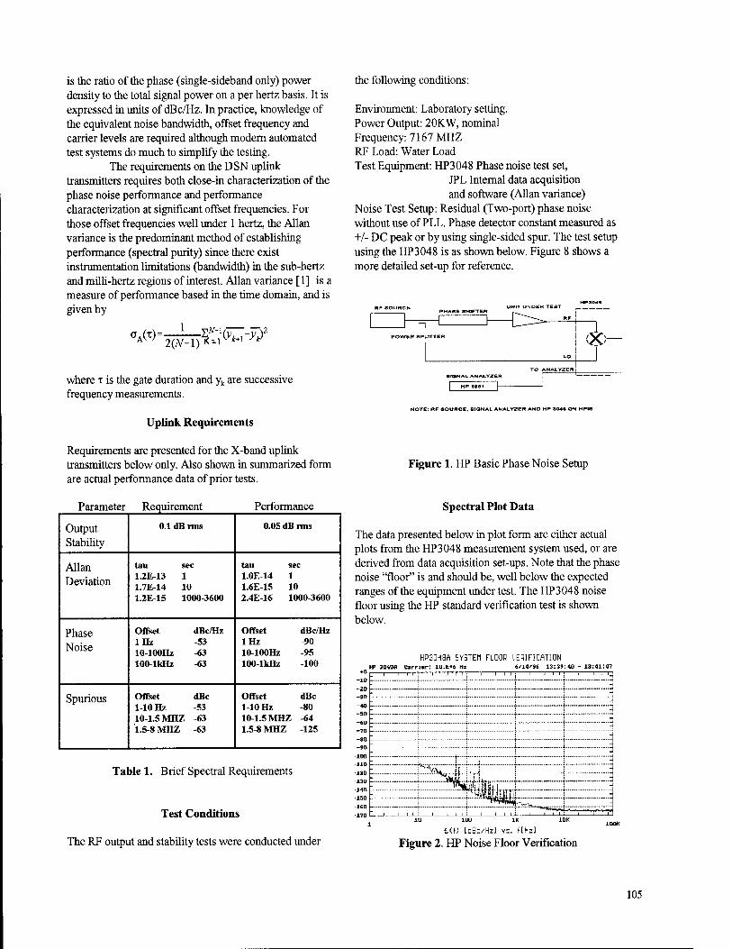
is the ratio of the phase (single-sideband only) power density to the total signal power on a per hertz basis. It is expressed in units of dBc/Hz. In practice, knowledge of the equivalent noise bandwidth, offset frequency and carrier levels are required although modern automated test systems do much to simplify the testing.
The requirements on the DSN uplink transmitters requires both close-in characterization of the phase noise performance and performance characterization at significant offset frequencies. For those offset frequencies well under 1 hertz, the Allan variance is the predominant method of establishing performance (spectral purity) since there exist instrumentation limitations (bandwidth) in the sub-hertz and milli-hertz regions of interest. Allan variance [ 1 ] is a measure of performance based in the time domain, and is given by
°A(T)=2(Fl)K^^)2
where i is the gate duration and yk are successive frequency measurements.
Uplink Requirements
the following conditions:
Environment: Laboratory setting. Power Output: 20KW, nominal Frequency: 7167 MHZ RF Load: Water Load Test Equipment: HP3048 Phase noise test set,
JPL Internal data acquisition and software (Allan variance)
Noise Test Setup: Residual (Two-port) phase noise without use of PLL. Phase detector constant measured as +/- DC peak or by using single-sided spur. The test setup using the HP3048 is as shown below. Figure 8 shows a more detailed set-up for reference.
RFSOURCE PHASE SHIFTER UNIT UNDER TEST
-Dr- POWER SPLITTER
TO ANALYZE R BIQNAL ANALYZER
&
NOTE: RF SOURCE. 6IONAL ANALYZER AND HP S04S ON HPIH
Requirements are presented for the X-band uplink transmitters below only. Also shown in summarized form are actual performance data of prior tests.
Figure 1. HP Basic Phase Noise Setup
Parameter Requirement Performance
Output Stability
0.1 dB rms 0.05 dB rms
Allan Deviation
tau sec 1.2E-13 1 1.7E-14 10 1.2E-15 1000-3600
tau sec 1.0E-14 1 1.6E-15 10 2.4E-16 1000-3600
Phase Noise
Offset dBc/Hz 1Hz -53 10-lOOHz -63 100-lkHz -63
Offset dBc/Hz 1Hz -90 10-lOOHz -95 100-lkHz -100
Spurious Offset dBc 1-10 Hz -53 10-1.5 MHZ -63 1.5-8 MHZ -63
Offset dBc 1-10 Hz -80 10-1.5 MHZ -64 1.5-8 MHZ -125
Table 1. Brief Spectral Requirements
Test Cpnditions
The RF output and stability tests were conducted under
Spectral Plot Data
The data presented below in plot form are either actual plots from the HP3048 measurement system used, or are derived from data acquisition set-ups. Note that the phase noise "floor" is and should be, well below the expected ranges of the equipment under test. The HP3048 noise floor using the HP standard verification test is shown below.
HP304BA SYSTEM FLOOR UEHIRCATI0N Carrisr: 10.E*6 Hz 6/14^96 13:39:40 - 13:41:47
10O 110
■120 130
■140 •150
160
■170
^ta^
Lit) [dBc/Hz] vs. tWzl
Figure 2. HP Noise Floor Verification
105
Note the major spurs at 60 and 120 Hz. These spurs are usually directly attributable to the AC power sources of the measurement system i.e., "instrumentation". The 20KW systems employ two modes of CW operation as described in the last power modulator symposium.. The primary mode is the "regulated" mode and is used for all missions. The active regulator ensures ripple performance better than 0.01% (approximately 1 v rms ripple) was described in the previous symposium. The alternate mode is the "regulator bypass" mode in which the active solid-state regulator is disabled and electrically bypassed. This results in the standard 12-pole rectifier topology with passive C-L (low-side)-C filtering. Ripple performance degrades approximately ten-fold. Additionally, plot data is broken down by AC or DC filament operation. Figure 3 now shows the spectral performance with AC filaments in regulator bypass mode. A 60Hz line is evident at -50.58 dBc/Hz. A couple of spurs of interest are the 30Hz and 420Hz spurs. The 30Hz spurs arises from the nature of the motor-generator set which supplies primary AC to the transformer- rectifier circuit under closed-loop control. Actually, the 30Hz spur is a sub-harmonic of the rotating (1800rpm) 7-pole generator which produces a 3-phase 0-480V 420Hz output. The subharmonic and the fundamental output frequency are related as
regulation loop. This is the case here with separate and independent floating AC filament bias applied at the klystron.
In the next plot, Figure 6, DC filament bias is used and again very real visual confirmation is given that the 60 Hz spur has virtually disappeared. Qualitatively, it is also seen that the harmonics of 60 Hz are somewhat reduced in that the "grass" level in the regulated mode DC filament noise plot is less intense when compared to the AC filament plot. It should be noted that the worst spur is at 420 Hz (-64.02 dBc/Hz) and just meets the - 63dBc/Hz phase noise requirement of Table 1. The uplink transmitters will be incorporating DC filaments as a result.
Allan Variance
Allan variances, o, of Table 1 are computed from a separately JPL generated test set (also used for phase noise) using a JPL generated executable program, (ADA source code), called ALLAN_TV.EXE. This generates an xxxx.pnb and the raw phase data is processed with Allan variance is reported as either sigma a or log o vs. tau, T. The data is processed as:
log(a) =\og((DatalN- \)m)
(mOrpm =30Hz
420/fe
and are always present but may be managed, to some extent, by additional filtering. Figure 4 now presents a similar plot but using DC filament power. It is noted that the 30Hz and 420Hz spurs are only slightly improved (~ 1.5-2 dB). What is important to note is that by simply inspecting at 60Hz, we see that the 60Hz spur evident in the previous plot is now completely removed. No line or hint of spurious activity is observed. This is a significant change for a relatively small change in operating posture (changing from AC to DC filament operation at the klystron cathode). In the next couple of plots, the operating mode is switched to the regulated mode. Figure 5 now shows the spectral plot with AC filament power. Due to regulation, the 30Hz spur is now at -73dBc/Hz, the 420Hz spur is at -62 dBc/Hz and the 60 Hz spur is at -51.42. When compared to the unregulated (AC filament) plot, it is seen that there is substantial (~ 15 dB) improvement at 30 and 420Hz. At 60Hz, however, the improvement is slight (<1 dB) suggesting that the active regulator, while having effect at 30 Hz, 420 Hz and so on, has no real effect at 60 Hz. The implication is, of course, that the 60 Hz source of excitation is outside the
where N is the number of samples at every data point where log (o) is to be computed. The program sets T at log intervals on up to 10000 seconds or higher with available memory. The tabulated data of Table 1 presents results for Allan variance and output stability. As shown, actual performance is better than the stated requirements and additional improvements can be approached through body coolant temperature control [2]. Figure 7 shows a complete wideband plot using the Allan variance data coupled with phase noise data using a JPL phase noise test set. Note the reduction in "grass" intensity; earlier plots show the interference caused by outside machinery (unknown at time of tests). On another note, an interesting exercise, (not done here), would be to compute Allan variance directly from spectral density by use of computer based algorithms [3].
Summary
Phase noise plots presented show differences in spectral performance as a function of power supply output (regulated vs. non-regulated operation) and filament bias. The plots suggest that improved load ripple performance and use of DC filament power reduces the spur content, completely eliminates 60Hz spurs and enhances Allan variance performance (close-in phase noise).
106
X-8AN0 PHASE NOISE! U/AC FILAMENTS (BYPASS MODE) HP 30«A Carrlf-r: 7.1«7E*9 It* 4/27/93 09:34:46 - 09:39:03
.^-Rnim PHASF mil SF U-ni" F f I nllFfJTc. -PFR nnnF ' HP 3048 0 CHI lar: 7.167E»? Hi 6/13/93 10:29:30 - 10:31:47
-100 -110
-120
:! ::::::^*ilfcwv !.IWfc
C<() CdBc/Hz) vs. KHz) £.((> IftHr-'H
Figure 3, PHASE NOISE (AC FIL, BYPASS MODE) Figure 7. "COMPLETE" PHASE NOISE PLOT
»BAND PHASE NOISE U/DC FILAMENTS (BYPASS HOOE) IP 3tHa« Carrlar: 7.167E.9 Hi 4/26/93 12:37:11 - 12:41:56
-«0 -70
-110 -120
-I-; 1 1—r-
^ .•r:. "....I. M J: - t-v
P^ oEvce
-D>
PT TEST POINT
7^
C=! £.'.() (dBc/Hzl vs. KHz)
Figure 4. PHASE NOISE (DC FIL, BYPASS MODE) Figure 8. STABILITY MEASUREMENT SYSTEM
X-BfiNO PHASE NOISE U-'AC FILAMENTS (PEG MODE) t*> 3048ft C*rrl«r: 7.1S7E*9 in 4/27/95 10:23:1B - 10:27:31
-100 -110 -120
b^r^^ !|H«I^
lOO IK 10«
tdl CdBc/Hz] vs. KHz]
Figure 5. PHASE NOISE (AC FIL, REG MODE)
Acknowledgments
The research described in this paper was carried out by the Jet Propulsion Laboratory, California Institute of Technology, under a contract with the National Aeronautics and Space Administration.
X-BAHO PHASE NOISE ll-DC FILAMENTS (REG MODE) If 3048a CMrrimr: 7.1«7E»9 Ifc 4^26/95 12:39:11 - 13:03:33
-100
-110
-120
lOO IK 10K
L'li [d8c/Hz] vs. KHz]
Figure 6. PHASE NOISE (DC FIL, REG MODE)
References
[ 1 ] D. W. Allan "Statistics of atomic frequency standards," Proc. IEEE, vol. 54 no. 2, pp. 221-230, Feb. 1966.
[2] R. M. Perez "Improvements in X-band transmitter phase stability through klystron body temperature regulation," TDA Progress Report 42-109, pp. 114-119, May 15, 1992 [JPL Internal Document]
[3] W. F. Egan "An efficient algorithm to compute Allan variance from spectral density," IEEE Trans. Instr. Meas., vol. 37 no. 2, 240-244, June 1988.
107
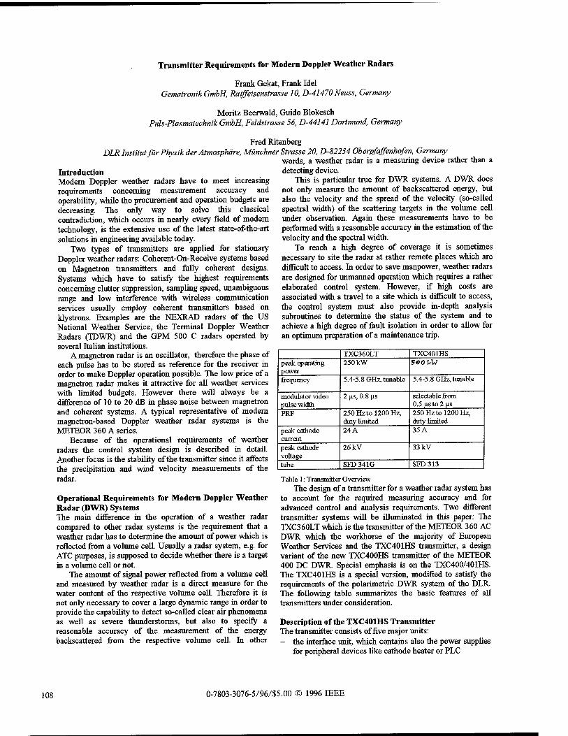
Transmitter Requirements for Modern Doppler Weather Radars
Frank Gekat, Frank Idel Gematronik GmbH, Raiffeisenstrasse 10, D-41470 Neuss, Germany
Moritz Beerwald, Guido Blokesch Puls-Plasmatechnik GmbH, Feldstrasse 56, D-44141 Dortmund, Germany
Fred Ritenberg DLR Institut fiir Physik der Atmosphäre, Münchner Strasse 20, D-82234 Oberpfaffenhofen, Germany
words, a weather radar is a measuring device rather than a
Introduction Modern Doppler weather radars have to meet increasing requirements concerning measurement accuracy and operability, while the procurement and operation budgets are decreasing. The only way to solve this classical contradiction, which occurs in nearly every field of modern technology, is the extensive use of the latest state-of-the-art solutions in engineering available today.
Two types of transmitters are applied for stationary Doppler weather radars: Coherent-On-Receive systems based on Magnetron transmitters and fully coherent designs. Systems which have to satisfy the highest requirements concerning clutter suppression, sampling speed, unambiguous range and low interference with wireless communication services usually employ coherent transmitters based on klystrons. Examples are the NEXRAD radars of the US National Weather Service, the Terminal Doppler Weather Radars (TDWR) and the GPM 500 C radars operated by several Italian institutions.
A magnetron radar is an oscillator, therefore the phase of each pulse has to be stored as reference for the receiver in order to make Doppler operation possible. The low price of a magnetron radar makes it attractive for all weather services with limited budgets. However there will always be a difference of 10 to 20 dB in phase noise between magnetron and coherent systems. A typical representative of modern magnetron-based Doppler weather radar systems is the METEOR 360 A series.
Because of the operational requirements of weather radars the control system design is described in detail. Another focus is the stability of the transmitter since it affects the precipitation and wind velocity measurements of the radar.
Operational Requirements for Modern Doppler Weather Radar (DWR) Systems The main difference in the operation of a weather radar compared to other radar systems is the requirement that a weather radar has to determine the amount of power which is reflected from a volume cell. Usually a radar system, e.g. for ATC purposes, is supposed to decide whether there is a target in a volume cell or not.
The amount of signal power reflected from a volume cell and measured by weather radar is a direct measure for the water content of the respective volume cell. Therefore it is not only necessary to cover a large dynamic range in order to provide the capability to detect so-called clear air phenomena as well as severe thunderstorms, but also to specify a reasonable accuracy of the measurement of the energy backscattered from the respective volume cell. In other
detecting device. This is particular true for DWR systems. A DWR does
not only measure the amount of backscattered energy, but also the velocity and the spread of the velocity (so-called spectral width) of the scattering targets in the volume cell under observation. Again these measurements have to be performed with a reasonable accuracy in the estimation of the velocity and the spectral width.
To reach a high degree of coverage it is sometimes necessary to site the radar at rather remote places which are difficult to access. In order to save manpower, weather radars are designed for unmanned operation which requires a rather elaborated control system. However, if high costs are associated with a travel to a site which is difficult to access, the control system must also provide in-depth analysis subroutines to determine the status of the system and to achieve a high degree of fault isolation in order to allow for an optimum preparation of a maintenance trip.
TXC360LT TXC401HS peak operating power
250 kW SOO\<\J
frequency 5.4-5.8 GHz, tunable 5.4-5.8 GHz, tunable
modulator video pulse width
2 us, 0.8 us selectable from 0.5 usto2 us
PRF 250 Hz to 1200 Hz, duty limited
250Hztol200Hz, duty limited
peak cathode current
24 A 35 A
peak cathode voltage
26 kV 33 kV
tube SED 341G SFD313
Table 1: Transmitter Overview The design of a transmitter for a weather radar system has
to account for the required measuring accuracy and for advanced control and analysis requirements. Two different transmitter systems will be illuminated in this paper: The TXC360LT which is the transmitter of the METEOR 360 AC DWR which the workhorse of the majority of European Weather Services and the TXC401HS transmitter, a design variant of the new TXC400HS transmitter of the METEOR 400 DC DWR. Special emphasis is on the TXC400/401HS. The TXC401HS is a special version, modified to satisfy the requirements of the polarimetric DWR system of the DLR. The following table summarizes the basic features of all transmitters under consideration.
Description of the TXC401HS Transmitter The transmitter consists of five major units: - the interface unit, which contains also the power supplies
for peripheral devices like cathode heater or PLC
108 0-7803-3076-5/96/S5.00 © 1996 IEEE
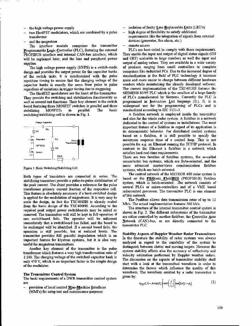
- the high voltage power supply - two HardFET modulators, which are combined by a pulse
transformer - and the magnetron
The interface module comprises the transmitter Programmable Logic Controller (PLC), featuring the external PROFE3US interface and internal CAN-bus interface, which will be explained later, and the bias and peripheral power supplies.
The high voltage power supply (HVPS) is a switch-mode design and provides the output power for the capacitor banks of the switch units. It is synchronized with the pulse repetition timing to ensure that the charging voltage of the capacitor banks is exactly the same from pulse to pulse regardless of variations in trigger timing due to staggering.
The HardFET modulators are the heart of the transmitter. They provide the switching and stabilization functionality as well as several test functions. Their key element is the switch board featuring three MOSFET switches in parallel and three stabilizing MOSFETs in parallel. The basic switching/stabilizing cell is shown in Fig. 1.
Charge Capaettor
Figure 1: Basic Switching/Stabilizing Cell
Both types of transistors are connected in series. The stabilizing transistors provide a pulse-to-pulse stabilization of the peak current. The shunt provides a reference for the pulse transformer primary current fraction of the respective cell. This feature is absolutely necessary if a hard-switched design is applied for the modulation of magnetrons. It is very easy to scale the design, in fact the TXC401HS is already scaled from the basic design of the TXC400HS. According to the required peak output power switchboards may be added or removed. The transmitter will still be kept in full operation if one switchboard fails. The operator will be informed immediately that a switchboard has failed, and the board to be exchanged will be identified. If a second board fails, the operation is still possible, but at reduced levels. The transmitter provides full graceful degradation which is an important feature for klystron systems, but it is also very useful for magnetron transmitters.
Another key element of the transmitter is the pulse transformer which features a very high transformation ratio of 1:100. The charging voltage of the switched capacitor bank is only 450 V, which is an important factor in the simple design of the modulator.
The Transmitter Control System The basic requirements of a DWR transmitter control system are - provision of local control Man-Machine Interfaces
(MMTs) for setup test and maintenance purposes
- isolation of faulty Line Replaceable Units (LRU's) - high degree of flexibility to satisfy additional
requirements like the integration of signals from external devices (generator, fire alarm, etc.)
- remote access PLCs are best-suited to comply with these requirements.
They enable the input and output of digital status signals (ON and OFF) scaleable to large numbers as well the input and output of analog values. They are available in a wide variety of products ranging from small controllers to complete computers like industrial PCs. Due to the increased degree of standardization in the field of PLC technology it becomes more and more easier to change between different hardware vendors while maintaining the already developed software. The current implementation of the TXC401HS features the SIEMENS S5/95 PLC which is the smallest of a large family of PLCs manufactured by Siemens. Currently the PLC is programmed in Instruction List language (IL). IL is in widespread use for the programming of PLCs and is standardized according to EEC 1131-3.
A fieldbus network is employed inside the transmitter and also for the whole radar system. A fieldbus is a network dedicated to the control of systems or installations. The most important feature of a fieldbus in regard of its application is its deterministic behavior. For distributed control systems based on a fieldbus, it is still possible to specify the maximum response time of a control loop. This is not possible for e.g. an Ethernet running the TCP/IP protocol. In contrast to the Ethernet a fieldbus is a network which satisfies hard real-time requirements. There are two families of fieldbus systems, the so-called sensor/actor bus systems, which are Byte-oriented, and the more advanced master/slave communication fieldbus systems, which are batch-oriented.
The control network of the METEOR 400 radar system is based on the PROcess FleldBUS (PROFE3US) fieldbus system, which is batch-oriented.. The network consists of several PLCs or micro-controllers and of a VME based radarcontrol processor. The transmitter PLC is one element of this network.
The Profibus allows data transmission rates of up to 12 Mb/s. The actual implementation features 500 kb/s.
The structure of the internal transmitter control system is shown in Fig. 2. The different subsystems of the transmitter are either controlled by another fieldbus, the Controller Area Network (CAN)-bus, or are directly connected to the transmitter PLC.
Stability Aspects of Doppler Weather Radar Transmitters In the literature the stability of radar systems was always analyzed in regard to the capability of the system to distinguish between clutter and moving targets. However the system stability affects also the accuracy of reflectivity and velocity estimation performed by Doppler weather radars. The discussion on the aspects of transmitter stability shall start with a look at the transmitted waveform in order to determine the factors which influence the quality of this waveform. The waveform emitted by a radar transmitter is given by:
(1) Sj-x(t,i) = Amp{Tj) reel ■fe)
sin(2s7/f + $j\
109
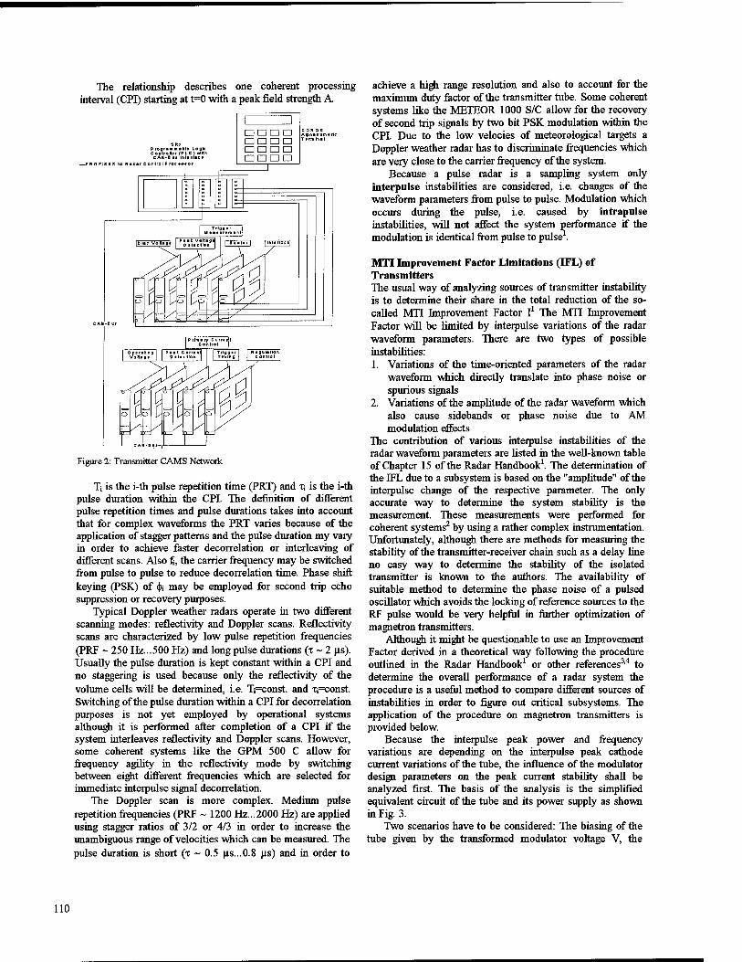
The relationship describes one coherent processing interval (CPI) starting at t=0 with a peak field strength A.
P rogram mable Leg Con troll - •-■ - CAK-B
PROriBUS to Radar Conti
1 1 □ □□a □ □□□ □ □□□ □ □□□
i
Figure 2: Transmitter CAMS Network
Ti is the i-th pulse repetition time (PRT) and n is the i-th pulse duration within the CPI. The definition of different pulse repetition times and pulse durations takes into account that for complex waveforms the PRT varies because of the application of stagger patterns and the pulse duration my vary in order to achieve faster decorrelation or interleaving of different scans. Also % the carrier frequency may be switched from pulse to pulse to reduce decorrelation time. Phase shift keying (PSK) of §i may be employed for second trip echo suppression or recovery purposes.
Typical Doppler weather radars operate in two different scanning modes: reflectivity and Doppler scans. Reflectivity scans are characterized by low pulse repetition frequencies (PRF ~ 250 Hz...500 Hz) and long pulse durations (x ~ 2 us). Usually the pulse duration is kept constant within a CPI and no staggering is used because only the reflectivity of the volume cells will be determined, i.e. Ti=const. and Tj=const. Switching of the pulse duration within a CPI for decorrelation purposes is not yet employed by operational systems although it is performed after completion of a CPI if the system interleaves reflectivity and Doppler scans. However, some coherent systems like the GPM 500 C allow for frequency agility in the reflectivity mode by switching between eight different frequencies which are selected for immediate interpulse signal decorrelation.
The Doppler scan is more complex. Medium pulse repetition frequencies (PRF ~ 1200 Hz...2000 Hz) are applied using stagger ratios of 3/2 or 4/3 in order to increase the unambiguous range of velocities which can be measured. The pulse duration is short (x ~ 0.5 us...0.8 us) and in order to
achieve a high range resolution and also to account for the maximum duty factor of the transmitter tube. Some coherent systems like the METEOR 1000 S/C allow for the recovery of second trip signals by two bit PSK modulation within the CPI. Due to the low velocies of meteorological targets a Doppler weather radar has to discriminate frequencies which are very close to the carrier frequency of the system.
Because a pulse radar is a sampling system only interpulse instabilities are considered, i.e. changes of the waveform parameters from pulse to pulse. Modulation which occurs during the pulse, i.e. caused by intrapulse instabilities, will not affect the system performance if the modulation is identical from pulse to pulse1.
MTI Improvement Factor Limitations (IFL) of Transmitters The usual way of analyzing sources of transmitter instability is to determine their share in the total reduction of the so- called MIT Improvement Factor I1 The MTI Improvement Factor will be limited by interpulse variations of the radar waveform parameters. There are two types of possible instabilities: 1. Variations of the time-oriented parameters of the radar
waveform which directly translate into phase noise or spurious signals
2. Variations of the amplitude of the radar waveform which also cause sidebands or phase noise due to AM modulation effects
The contribution of various interpulse instabilities of the radar waveform parameters are listed in the well-known table of Chapter 15 of the Radar Handbook1. The determination of the IFL due to a subsystem is based on the "amplitude" of the interpulse change of the respective parameter. The only accurate way to determine the system stability is the measurement. These measurements were performed for coherent systems2 by using a rather complex instrumentation. Unfortunately, although there are methods for measuring the stability of the transmitter-receiver chain such as a delay line no easy way to determine the stability of the isolated transmitter is known to the authors. The availability of suitable method to determine the phase noise of a pulsed oscillator which avoids the locking of reference sources to the RF pulse would be very helpful in further optimization of magnetron transmitters.
Although it might be questionable to use an Improvement Factor derived in a theoretical way following the procedure outlined in the Radar Handbook1 or other references3'4 to determine the overall performance of a radar system the procedure is a useful method to compare different sources of instabilities in order to figure out critical subsystems. The application of the procedure on magnetron transmitters is provided below.
Because the interpulse peak power and frequency variations are depending on the interpulse peak cathode current variations of the tube, the influence of the modulator design parameters on the peak current stability shall be analyzed first. The basis of the analysis is the simplified equivalent circuit of the tube and its power supply as shown in Fig. 3.
Two scenarios have to be considered: The biasing of the tube given by the transformed modulator voltage V, the
110

internal static impedance of the modulator Zi and the static load impedance ZL.
^■\
Figure 3: Modulator-Load Equivalent Circuit
The small-signal behavior is determined by the interpulse modulator voltage variation AV, the internal dynamic impedance of the modulator zi and the dynamic load impedance ZL. Thus the peak load current variation AIL is:
(2) A/L = /L AV Zt + ZL
V z, + zL
ZL is calculated from the tube cathode voltage and the peak cathode current in the bias point. If a dequing-stabilized line- type modulator is considered, V is the transformed charging voltage (which is twice epy in the bias point) and Zi is the transformed PFN impedance which is approximately equal to ZL if matching is assumed. For line-type modulators static and dynamic impedance are the same. The following numbers taken from the METEOR 360 AC magnetron transmitter TXC360LT may serve as an example: modulator voltage stability AV/V peak cathode current II
transformed PFN impedance Zi (=ZL)
dynamic load impedance ZL
resulting peak current variation
0.1% 24 A l.i kn 70 Q 45 mA
Table 2: TXC360LT Operating Conditions
The current stability of the TXC401HS transmitter is provided by means of interpulse current stabilization. The numbers are as follows: peak cathode current II 35 A peak cathode current stability Ali/ II 0.1 % resulting peak current variation 35 mA
Table 3: TXC401HS Operating Conditions
Transmitter Frequency It is assumed that the frequency stability of the magnetron is determined solely by the pushing figure PF=Af/AI. By means of the duplexer the tube is decoupled from the waveguide run to the antenna, therefore the pulling figure may be neglected. Frequency changes due to thermal variations could be ignored on the time scale under consideration. Influences of heater current variations will also be neglected because DC heating with low ripple is applied. Thus If is calculated from:
(3) / =10log(l/(^Afr))2
TXC360LT TXC401HS pushing figure PF 100 kHz/A 100 kHz/A frequency variations Af 4.5 kHz 3.5 kHz
pulse duration T 0.8 ns 0.8 us
IFLIt 38.9 dB 41 dB
Table 4: IFL due to Frequency Variations
Care has to be taken in comparing the figures of the table.4 The TXC401HS transmitter is more stable although the
current variation is more than for the TXC360LT, i.e. the difference in IFL will be much more if the TXC400HS is compared to its precessor. Transmitter Phase Shift The interpulse phase shift of a magnetron transmitter is random. Therefore it is necessary to provide a phase reference for each pulse which is accomplished by means of an injection-locked COHO. Thus this instability is subject of a receiver analysis and will not be considered here.
Transmitter Amplitude The amplitude of the emitted field of the magnetron is proportional to the cathode current:
AAIA=AICIIC (5)
The resulting IFL is derived from:
lA=10\og(AlAÄ)2 (6)
The respective numbers for the IFL IA using the values listed above are: TXC360LT: 54.5 dB TXC401HS: 60 dB
Pulse Timing The IFL due to pulse repetition timing jitter is:
/PR7-=10log(w(V2A7-)) (7)
Two components are influencing the trigger jitter of a magnetron transmitter: the trigger jitter of the switch and the oscillation onset jitter of the tube. Typical numbers for the systems considered here are listed in Tab. 5 together with indications for the affected systems.
Trigger Jitter
IFL TXC 36GXT
TXC 401HS
Magnetron 2ns 49 dB X X
Thyratron 2ns 49 dB X
MOSFET < 0.5 ns 61 dB X
Table 5: IFL due to Pulse Timing Jitter
Pulse Width Line-Type designs like the modulator of the TXC360LT are not affected by pulse width jitter because their pulse duration is determined by passive components only. However, pulse width variations have to be considered for hard-switched systems like the TXC401HS.
The respective IFL is:
/T=10log(r/Ar)2 (8)
The numbers for the TXC401HS are: Pulse Width Jitter: < 0.5 ns IFL It: 64 dB
The inverse of the total IFL is equal to the sum of the log arguments i p=101og(i)] provided above:
/rx=10log^1/(zy)] (9)
The resulting IFLs for the transmitters under consideration are listed below: TXC360LT: 38 dB TXC401HS: 40 dB The calculation of the total LFL according to (9) is only valid, if the contributing factors are statistically independent. The is
111
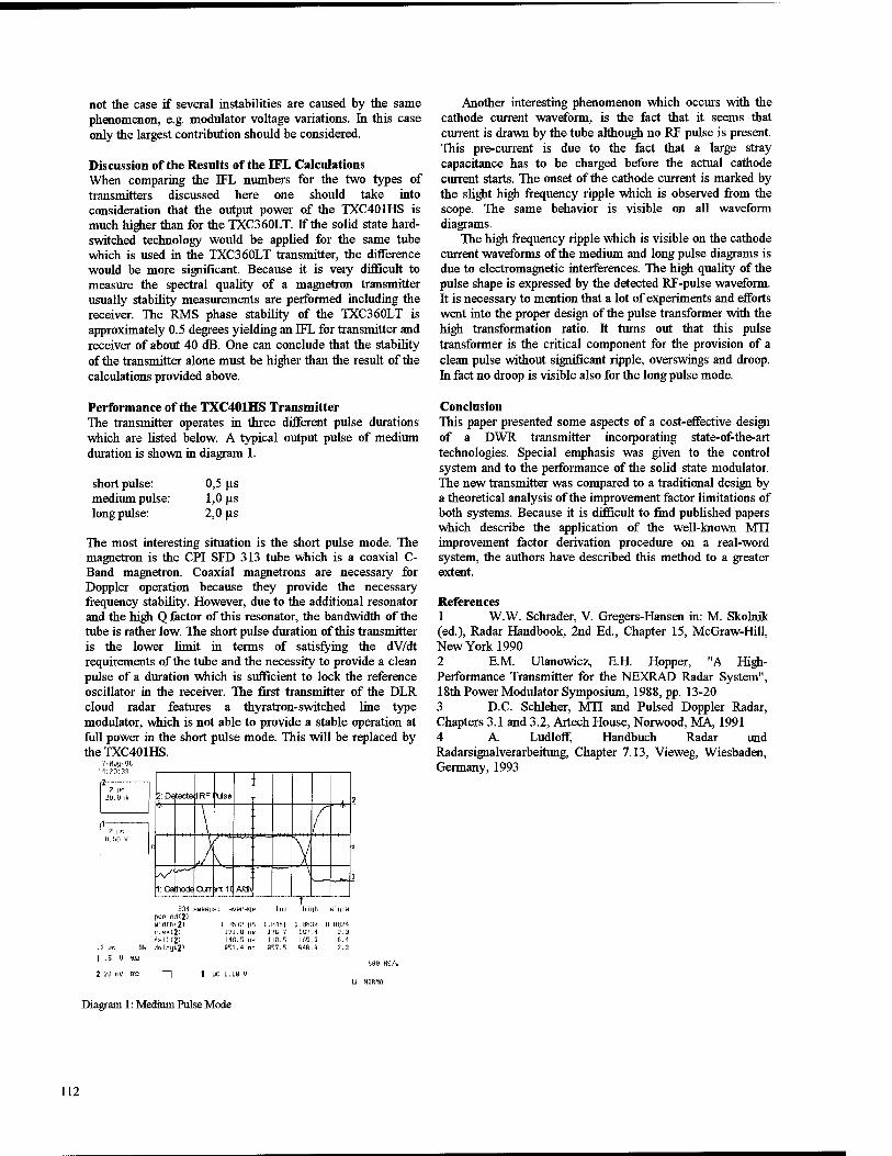
not the case if several instabilities are caused by the same phenomenon, e.g. modulator voltage variations. In this case only the largest contribution should be considered.
Discussion of the Results of the IFL Calculations When comparing the IFL numbers for the two types of transmitters discussed here one should take into consideration that the output power of the TXC401HS is much higher than for the TXC360LT. If the solid state hard- switched technology would be applied for the same tube which is used in the TXC360LT transmitter, the difference would be more significant. Because it is very difficult to measure the spectral quality of a magnetron transmitter usually stability measurements are performed including the receiver. The RMS phase stability of the TXC360LT is approximately 0.5 degrees yielding an IFL for transmitter and receiver of about 40 dB. One can conclude that the stability of the transmitter alone must be higher than the result of the calculations provided above.
Another interesting phenomenon which occurs with the cathode current waveform, is the fact that it seems that current is drawn by the tube although no RF pulse is present. This pre-current is due to the fact that a large stray capacitance has to be charged before the actual cathode current starts. The onset of the cathode current is marked by the slight high frequency ripple which is observed from the scope. The same behavior is visible on all waveform diagrams.
The high frequency ripple which is visible on the cathode current waveforms of the medium and long pulse diagrams is due to electromagnetic interferences. The high quality of the pulse shape is expressed by the detected RF-pulse waveform. It is necessary to mention that a lot of experiments and efforts went into the proper design of the pulse transformer with the high transformation ratio. It turns out that this pulse transformer is the critical component for the provision of a clean pulse without significant ripple, overswings and droop. In fact no droop is visible also for the long pulse mode.
Performance of the TXC401HS Transmitter The transmitter operates in three different pulse durations which are listed below. A typical output pulse of medium duration is shown in diagram 1.
short pulse: medium pulse: long pulse:
0,5 us 1,0 ns 2,0 ns
The most interesting situation is the short pulse mode. The magnetron is the CPI SFD 313 tube which is a coaxial C- Band magnetron. Coaxial magnetrons are necessary for Doppler operation because they provide the necessary frequency stability. However, due to the additional resonator and the high Q factor of this resonator, the bandwidth of the tube is rather low. The short pulse duration of this transmitter is the lower limit in terms of satisfying the dV/dt requirements of the tube and the necessity to provide a clean pulse of a duration which is sufficient to lock the reference oscillator in the receiver. The first transmitter of the DLR cloud radar features a thyratron-switched line type modulator, which is not able to provide a stable operation at full power in the short pulse mode. This will be replaced by theTXC401HS.
Conclusion This paper presented some aspects of a cost-effective design of a DWR transmitter incorporating state-of-the-art technologies. Special emphasis was given to the control system and to the performance of the solid state modulator. The new transmitter was compared to a traditional design by a theoretical analysis of the improvement factor limitations of both systems. Because it is difficult to find published papers which describe the application of the well-known MIT improvement factor derivation procedure on a real-word system, the authors have described this method to a greater extent.
References 1 W.W. Schrader, V. Gregers-Hansen in: M. Skolnik (ed.), Radar Handbook, 2nd Ed., Chapter 15, McGraw-Hill, New York 1990 2 E.M. Ulanowicz, E.H. Hopper, "A High- Performance Transmitter for the NEXRAD Radar System", 18th Power Modulator Symposium, 1988, pp. 13-20 3 D.C. Schleher, MTI and Pulsed Doppler Radar, Chapters 3.1 and 3.2, Artech House, Norwood, MA, 1991 4 A. Ludloff Handbuch Radar und Radarsignalverarbeitung, Chapter 7.13, Vieweg, Wiesbaden, Germany, 1993
Diagram 1: Medium Pulse Mode
112
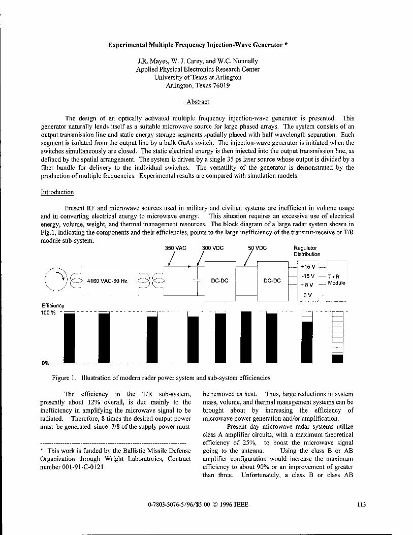
Experimental Multiple Frequency Injection-Wave Generator *
J.R. Mayes, W. J. Carey, and W.C. Nunnally Applied Physical Electronics Research Center
University of Texas at Arlington Arlington, Texas 76019
Abstract
The design of an optically activated multiple frequency injection-wave generator is presented. This generator naturally lends itself as a suitable microwave source for large phased arrays. The system consists of an output transmission line and static energy storage segments spatially placed with half wavelength separation. Each segment is isolated from the output line by a bulk GaAs switch. The injection-wave generator is initiated when the switches simultaneously are closed. The static electrical energy is then injected into the output transmission line, as defined by the spatial arrangement. The system is driven by a single 35 ps laser source whose output is divided by a fiber bundle for delivery to the individual switches. The versatility of the generator is demonstrated by the production of multiple frequencies. Experimental results are compared with simulation models.
Introduction
Present RF and microwave sources used in military and civilian systems are inefficient in volume usage and in converting electrical energy to microwave energy. This situation requires an excessive use of electrical energy, volume, weight, and thermal management resources. The block diagram of a large radar system shown in Fig.l, indicating the components and their efficiencies, points to the large inefficiency of the transmit-receive or T/R module sub-system.
350 VAC 300 VDC 50VDC Regulator / Distribution / .A
4160VAC-60HZ DC-DC DC-DC
+15 V
-15 V + 8V
0V
T/R Module
Efficiency 100%
Figure 1. Illustration of modern radar power system and sub-system efficiencies
The efficiency in the T/R sub-system, presently about 12% overall, is due mainly to the inefficiency in amplifying the microwave signal to be radiated. Therefore, 8 times the desired output power must be generated since 7/8 of the supply power must
* This work is funded by the Ballistic Missile Defense Organization through Wright Laboratories, Contract number 001-9 l-C-0121
be removed as heat. Thus, large reductions in system mass, volume, and thermal management systems can be brought about by increasing the efficiency of microwave power generation and/or amplification.
Present day microwave radar systems utilize class A amplifier circuits, with a maximum theoretical efficiency of 25%, to boost the microwave signal going to the antenna. Using the class B or AB amplifier configuration would increase the maximum efficiency to about 90% or an improvement of greater than three. Unfortunately, a class B or class AB
0-7803-3076-5/96/S5.00 © 1996 IEEE 113
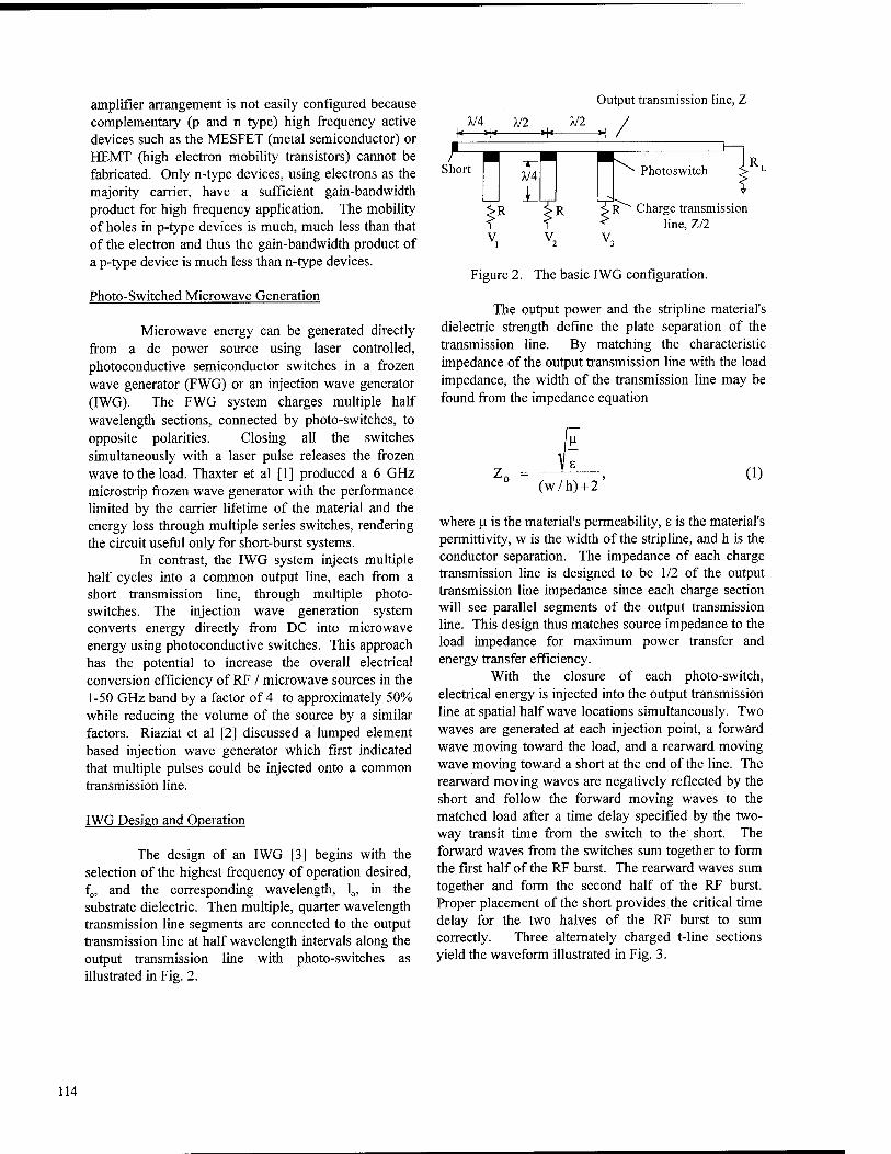
amplifier arrangement is not easily configured because complementary (p and n type) high frequency active devices such as the MESFET (metal semiconductor) or HEMT (high electron mobility transistors) cannot be fabricated. Only n-type devices, using electrons as the majority carrier, have a sufficient gain-bandwidth product for high frequency application. The mobility of holes in p-type devices is much, much less than that of the electron and thus the gain-bandwidth product of a p-type device is much less than n-type devices.
Photo-Switched Microwave Generation
Microwave energy can be generated directly from a dc power source using laser controlled, photoconductive semiconductor switches in a frozen wave generator (FWG) or an injection wave generator (IWG). The FWG system charges multiple half wavelength sections, connected by photo-switches, to opposite polarities. Closing all the switches simultaneously with a laser pulse releases the frozen wave to the load. Thaxter et al [1] produced a 6 GHz microstrip frozen wave generator with the performance limited by the carrier lifetime of the material and the energy loss through multiple series switches, rendering the circuit useful only for short-burst systems.
In contrast, the IWG system injects multiple half cycles into a common output line, each from a short transmission line, through multiple photo- switches. The injection wave generation system converts energy directly from DC into microwave energy using photoconductive switches. This approach has the potential to increase the overall electrical conversion efficiency of RF / microwave sources in the 1-50 GHz band by a factor of 4 to approximately 50% while reducing the volume of the source by a similar factors. Riaziat et al [2] discussed a lumped element based injection wave generator which first indicated that multiple pulses could be injected onto a common transmission line.
IWG Design and Operation
The design of an IWG [3] begins with the selection of the highest frequency of operation desired, f0, and the corresponding wavelength, 10, in the substrate dielectric. Then multiple, quarter wavelength transmission line segments are connected to the output transmission line at half wavelength intervals along the output transmission line with photo-switches as illustrated in Fig. 2.
Output transmission line, Z
A/4 111 m \* <+< H* H
F Short
X74
L TR ?R F V. V,
Photoswitch
Charge transmission line, Z/2
V,
Figure 2. The basic IWG configuration.
The output power and the stripline material's dielectric strength define the plate separation of the transmission line. By matching the characteristic impedance of the output transmission line with the load impedance, the width of the transmission line may be found from the impedance equation
z„ = ';
(w/h) + 2 (1)
where \x is the material's permeability, s is the material's permittivity, w is the width of the stripline, and h is the conductor separation. The impedance of each charge transmission line is designed to be 1/2 of the output transmission line impedance since each charge section will see parallel segments of the output transmission line. This design thus matches source impedance to the load impedance for maximum power transfer and energy transfer efficiency.
With the closure of each photo-switch, electrical energy is injected into the output transmission line at spatial half wave locations simultaneously. Two waves are generated at each injection point, a forward wave moving toward the load, and a rearward moving wave moving toward a short at the end of the line. The rearward moving waves are negatively reflected by the short and follow the forward moving waves to the matched load after a time delay specified by the two- way transit time from the switch to the short. The forward waves from the switches sum together to form the first half of the RF burst. The rearward waves sum together and form the second half of the RF burst. Proper placement of the short provides the critical time delay for the two halves of the RF burst to sum correctly. Three alternately charged t-line sections yield the waveform illustrated in Fig. 3.
114
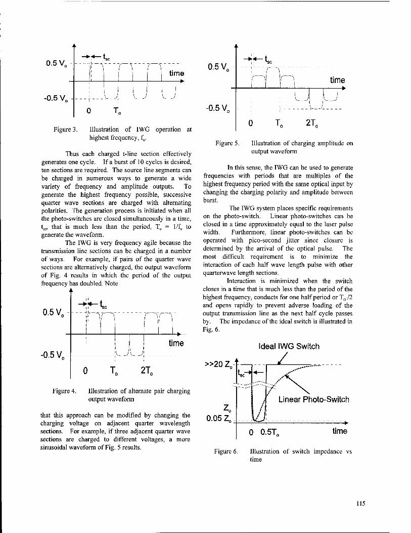
d k
0.5 V0
l
—* 1
tsc ~-r— —
time
0.5 V0-
l l
l \ __u 0 T0
Figure 3. Illustration of IWG highest frequency, f0.
operation at
Thus each charged t-line section effectively generates one cycle. If a burst of 10 cycles is desired, ten sections are required. The source line segments can be charged in numerous ways to generate a wide variety of frequency and amplitude outputs. To generate the highest frequency possible, successive quarter wave sections are charged with alternating polarities. The generation process is initiated when all the photo-switches are closed simultaneously in a time, tsc, that is much less than the period, T0 = l/f0 to generate the waveform.
The IWG is very frequency agile because the transmission line sections can be charged in a number of ways. For example, if pairs of the quarter wave sections are alternatively charged, the output waveform of Fig. 4 results in which the period of the output frequency has doubled. Note
0.5 V,
-0.5 V,
Figure 4. Illustration of alternate pair charging output waveform
that this approach can be modified by changing the charging voltage on adjacent quarter wavelength sections. For example, if three adjacent quarter wave sections are charged to different voltages, a more sinusoidal waveform of Fig. 5 results.
i,
0.5 V0
-*> 1
1
1,
1/
«-U
time
0 5V
1 '11 1 1 \ 11 I 1
i i lV J U.vJ v0 1
0 T0 2T0
Figure 5. Illustration of charging amplitude on output waveform
In this sense, the IWG can be used to generate frequencies with periods that are multiples of the highest frequency period with the same optical input by changing the charging polarity and amplitude between burst.
The IWG system places specific requirements on the photo-switch. Linear photo-switches can be closed in a time approximately equal to the laser pulse width. Furthermore, linear photo-switches can be operated with pico-second jitter since closure is determined by the arrival of the optical pulse. The most difficult requirement is to minimize the interaction of each half wave length pulse with other quarterwave length sections.
Interaction is minimized when the switch closes in a time that is much less than the period of the highest frequency, conducts for one half period or T012 and opens rapidly to prevent adverse loading of the output transmission line as the next half cycle passes by. The impedance of the ideal switch is illustrated in Fig. 6.
»20 Z,
Ideal IWG Switch
Z
0.05 Z,
0 0.5T,
Figure 6. Illustration of switch impedance vs time
115
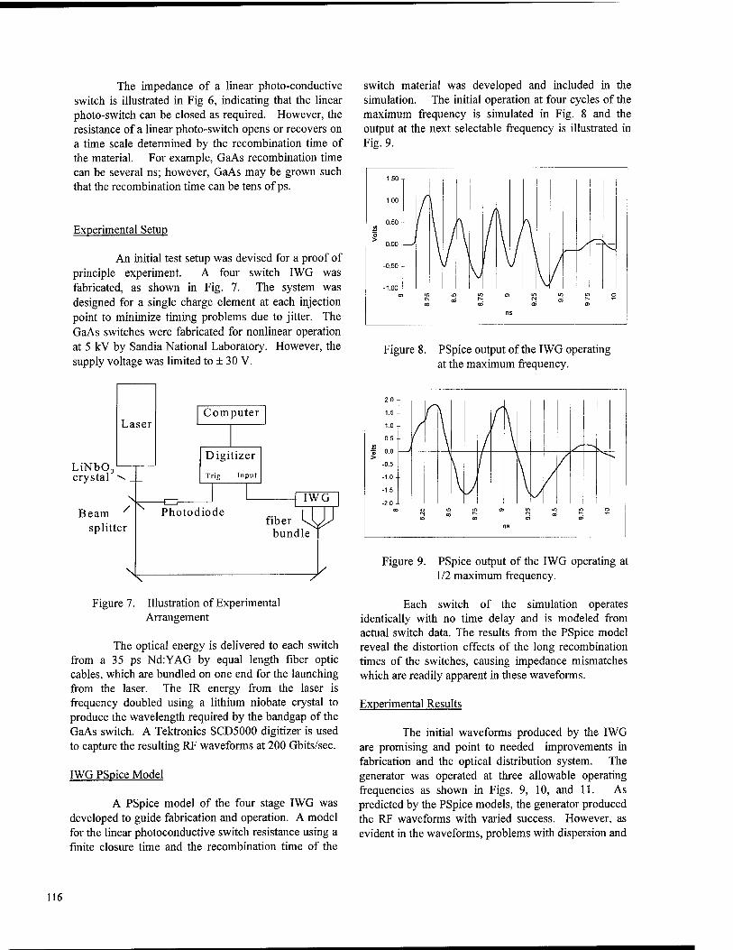
The impedance of a linear photo-conductive switch is illustrated in Fig 6, indicating that the linear photo-switch can be closed as required. However, the resistance of a linear photo-switch opens or recovers on a time scale determined by the recombination time of the material. For example, GaAs recombination time can be several ns; however, GaAs may be grown such that the recombination time can be tens of ps.
Experimental Setup
An initial test setup was devised for a proof of principle experiment. A four switch IWG was fabricated, as shown in Fig. 7. The system was designed for a single charge element at each injection point to minimize timing problems due to jitter. The GaAs switches were fabricated for nonlinear operation at 5 kV by Sandia National Laboratory. However, the supply voltage was limited to + 30 V.
Computer
LiNbOj crystal \__
Beam /
splitter
Digitizer
Trig Input
-CD Photodiode
IWG
fiber bundle SP
Figure 7. Illustration of Experimental Arrangement
The optical energy is delivered to each switch from a 35 ps Nd:YAG by equal length fiber optic cables, which are bundled on one end for the launching from the laser. The IR energy from the laser is frequency doubled using a lithium niobate crystal to produce the wavelength required by the bandgap of the GaAs switch. A Tektronics SCD5000 digitizer is used to capture the resulting RF waveforms at 200 Gbits/sec.
IWG PSpice Model
A PSpice model of the four stage IWG was developed to guide fabrication and operation. A model for the linear photoconductive switch resistance using a finite closure time and the recombination time of the
switch material was developed and included in the simulation. The initial operation at four cycles of the maximum frequency is simulated in Fig. 8 and the output at the next selectable frequency is illustrated in Fig. 9.
Figure 8. PSpice output of the IWG operating at the maximum frequency.
2.0
1.5 -
1.0 -
0.5 - in % 0.0 >
-0.5
-1.0
-1.5
-2.0 CO
I /
f \
X CO r-
DO
/
ns CT>
s/
o
Figure 9. PSpice output of the IWG operating at 1/2 maximum frequency.
Each switch of the simulation operates identically with no time delay and is modeled from actual switch data. The results from the PSpice model reveal the distortion effects of the long recombination times of the switches, causing impedance mismatches which are readily apparent in these waveforms.
Experimental Results
The initial waveforms produced by the IWG are promising and point to needed improvements in fabrication and the optical distribution system. The generator was operated at three allowable operating frequencies as shown in Figs. 9, 10, and 11. As predicted by the PSpice models, the generator produced the RF waveforms with varied success. However, as evident in the waveforms, problems with dispersion and
116
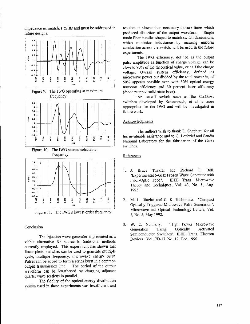
impedance mismatches exists and must be addressed in future designs.
Figure 9. The IWG operating at maximum frequency.
2.5 ,
2
1.5
1
| 0.5
0
-0.5
-1 -
-1.5 a o I-
/
f \ /
*\
s o CO
It
\
C cn
t «a
15
C
\
c
_> /
c : !
Figure 10. The IWG second selectable frequency.
1.2 -,
1
0.8
0.6
« 0.4
> 0.2
)
(
V ">
\
-0.2
-0.4
-0.6 r- oi o r-
(O a r--
o 00
to CM m o cn
IS
c Ul GO cn
co o c
If c
Figure 11. The IWG's lowest order frequency.
resulted in slower than necessary closure times which produced distortion of the output waveform. Single mode fiber bundles shaped to match switch dimensions, which minimize inductance by insuring uniform conduction across the switch, will be used in the future experiments.
The IWG efficiency, defined as the output pulse amplitude as function of charge voltage, can be close to 90% of the theoretical value, or half the charge voltage. Overall system efficiency, defined as microwave power out divided by the total power in, of 50% appears possible even with 50% optical energy transport efficiency and 30 percent laser efficiency (diode pumped solid state laser).
An on-off switch such as the Cu:GaAs switches developed by Schoenbach, et al is more appropriate for the IWG and will be investigated in future work.
Acknowledgments
The authors wish to thank L. Shepherd for all his invaluable assistance and to G. Loubriel and Sandia National Laboratory for the fabrication of the GaAs switches.
References
1. J. Bruce Thaxter and Richard E. Bell. "Experimental 6-GHz Frozen Wave Generator with Fiber-Optic Feed". IEEE Trans. Microwave Theory and Techniques, Vol. 43, No. 8, Aug. 1995.
2. M. L. Riaziat and C. K. Nishimoto. "Compact Optically Triggered Microwave Pulse Generation". Microwave and Optical Technology Letters, Vol. 5, No. 5, May 1992.
Conclusion
The injection wave generator is presented as a viable alternative RF source to traditional methods currently employed. This experiment has shown that linear photo-switches can be used to generate multiple cycle, multiple frequency, microwave energy burst. Pulses can be added to form a series burst in a common output transmission line. The period of the output waveform can be lengthened by charging adjacent quarter wave sections in parallel.
The fidelity of the optical energy distribution system used in these experiments was insufficient and
3. W. C. Nunnally. "High Power Microwave Generation Using Optically Activated Semiconductor Switches". IEEE Trans. Electron Devices. Vol. ED-17, No. 12. Dec. 1990.
117

Power modulator for broadband agile mirror radar utilizing semiconductor switching
M. C. Myers, R. F. Fernsler, J. A. Gregor, J. Mathew, R. A. Meger, D. P. Murphy, and R. E. Pechacek
Plasma Physics Division, Code 6750 Naval Research Laboratory, Washington, D.C. 20375-5346
Power modulators have been designed which can generate fast rising, high voltage pulses up to 10 kV with arbitrary pulse widths at pulse repetition frequencies greater than 5 kHz. The design utilizes series IGBT switching. The modulators drive the NRL Agile Mirror experiment - an electronically steered sheet plasma which can be used to direct a microwave beam for radar and communications applications.
Introduction
A sheet plasma of sufficient density can be used to direct a microwave beam for radar and communications applications.1 Such a "plasma mirror" is generated using high voltage, fast rise time, variable width pulses at high pulse repetition frequencies (PRF). In addition, the plasma mirror must be steerable or agile in both azimuth and altitude. The Agile Mirror Experiment at NRL has produced a planar 60 x 60 cm sheet plasma capable of directing X-band microwaves.2
The present modulator design uses a Crossatron3 as the primary switching element. Although the Crossatron is rugged and reliable, it is also very expensive and the typical voltage drop across the tube approaches 500 Volts. The next generation Agile Mirror requires multiple modulators to drive a cathode array to demonstrate azimuthal agility. Thus, it is desirable and cost effective to consider power semiconductor switching as an alternative. The insulated gate bipolar transistor (IGBT) was chosen for this application due to it's high current capacity and high frequency capability at voltages of 1.2-1.6 kV. Since several kilovolts are needed to generate the sheet plasma, a series connection of IGBTs is required. The
switching design includes careful consideration of voltage sharing in steady state and during the switching transient as well as gate drive circuit and thermal issues.
Agile Mirror Experiment
A plasma distribution presents an interesting way to direct electromagnetic waves. Since the plasma is effectively without inertia, it can in principle be electronically steered to illuminate and receive with great agility (i.e. it can be formed in one location to reflect a radar beam for targeting, turned off for a short duration, and then reformed in another orientation for receiving the radar echo). The distribution also provides broadband and high power handling capability. To reflect incident electromagnetic radiation, a plasma must have a density greater than the critical density nc = mee0CD21 e2. For incident X-band (8.2-12.4 GHz) microwaves, «c=1.2xl0~12 cm"3. The distribution must be reproducible and have a size which is large compared to the longest wavelength used while being flat on a scale length smaller than the shortest wavelength used.
The NRL Agile Mirror is a 60 x 60 cm plasma sheet distribution created in a vacuum chamber at pressures of 100-200 mTorr.
118 U.S. Government work not protected by U.S. copyright
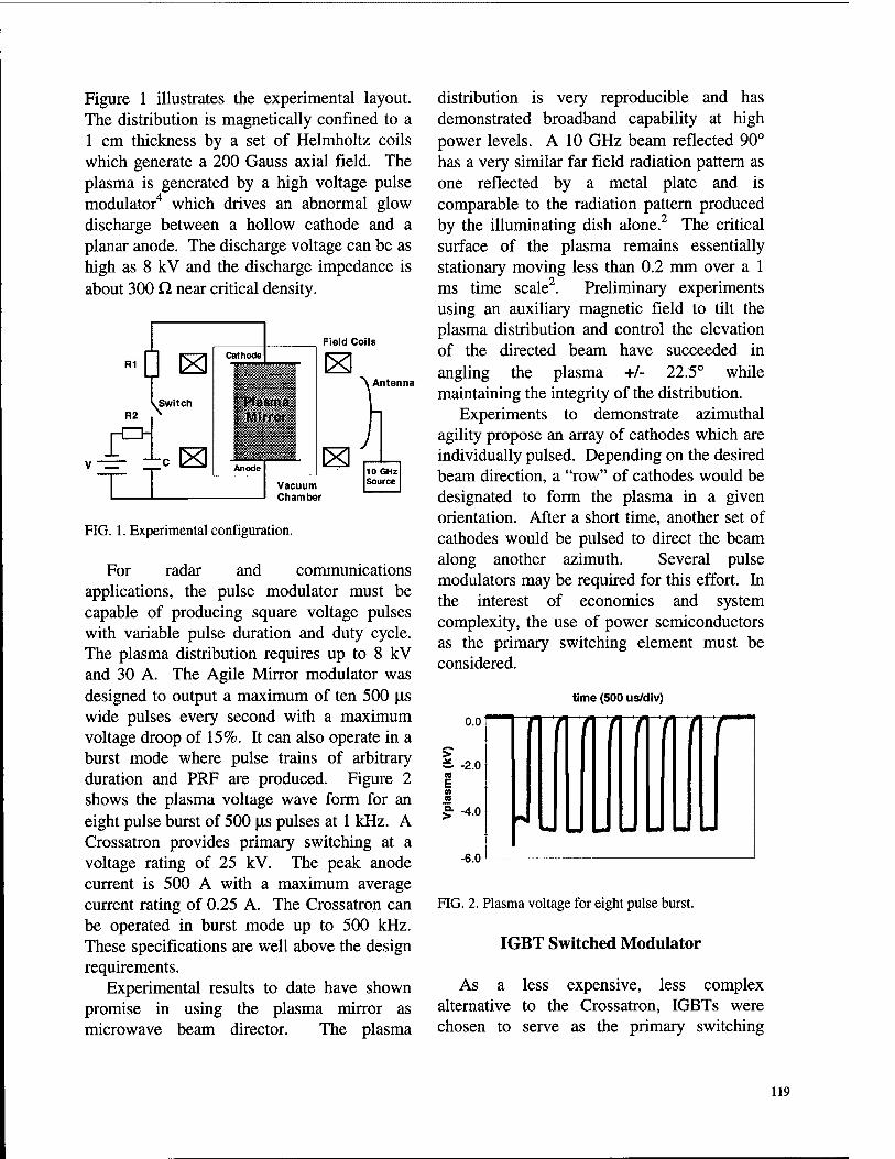
Figure 1 illustrates the experimental layout. The distribution is magnetically confined to a 1 cm thickness by a set of Helmholtz coils which generate a 200 Gauss axial field. The plasma is generated by a high voltage pulse modulator4 which drives an abnormal glow discharge between a hollow cathode and a planar anode. The discharge voltage can be as high as 8 kV and the discharge impedance is about 300 Q near critical density.
R1
.Switch R2 .
4B
Cathode
| Plasma I Mirror i
Field Coils
\ Antenna
h Vacuum Chamber
10 GHz Source
FIG. 1. Experimental configuration.
For radar and communications applications, the pulse modulator must be capable of producing square voltage pulses with variable pulse duration and duty cycle. The plasma distribution requires up to 8 kV and 30 A. The Agile Mirror modulator was designed to output a maximum of ten 500 (is wide pulses every second with a maximum voltage droop of 15%. It can also operate in a burst mode where pulse trains of arbitrary duration and PRF are produced. Figure 2 shows the plasma voltage wave form for an eight pulse burst of 500 \is pulses at 1 kHz. A Crossatron provides primary switching at a voltage rating of 25 kV. The peak anode current is 500 A with a maximum average current rating of 0.25 A. The Crossatron can be operated in burst mode up to 500 kHz. These specifications are well above the design requirements.
Experimental results to date have shown promise in using the plasma mirror as microwave beam director. The plasma
distribution is very reproducible and has demonstrated broadband capability at high power levels. A 10 GHz beam reflected 90° has a very similar far field radiation pattern as one reflected by a metal plate and is comparable to the radiation pattern produced by the illuminating dish alone.2 The critical surface of the plasma remains essentially stationary moving less than 0.2 mm over a 1 ms time scale2. Preliminary experiments using an auxiliary magnetic field to tilt the plasma distribution and control the elevation of the directed beam have succeeded in angling the plasma +/- 22.5° while maintaining the integrity of the distribution.
Experiments to demonstrate azimuthal agility propose an array of cathodes which are individually pulsed. Depending on the desired beam direction, a "row" of cathodes would be designated to form the plasma in a given orientation. After a short time, another set of cathodes would be pulsed to direct the beam along another azimuth. Several pulse modulators may be required for this effort. In the interest of economics and system complexity, the use of power semiconductors as the primary switching element must be considered.
time (500 us/div)
FIG. 2. Plasma voltage for eight pulse burst.
IGBT Switched Modulator
As a less expensive, less complex alternative to the Crossatron, IGBTs were chosen to serve as the primary switching
119
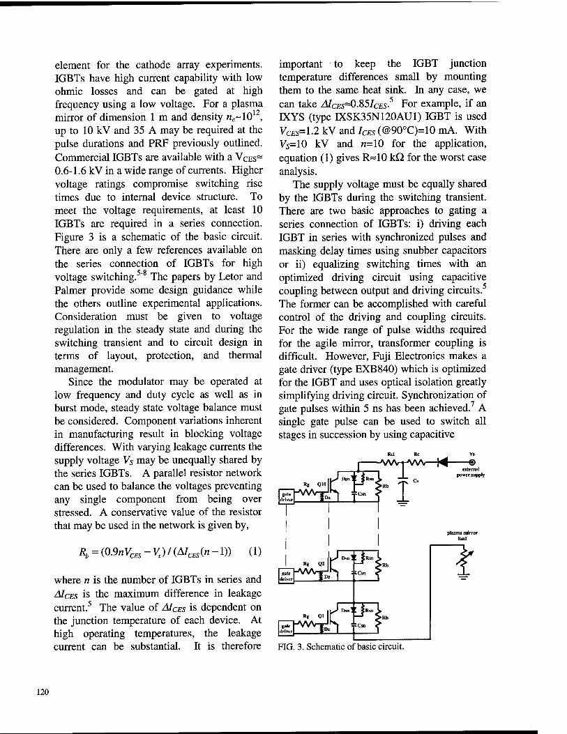
element for the cathode array experiments. IGBTs have high current capability with low ohmic losses and can be gated at high frequency using a low voltage. For a plasma mirror of dimension 1 m and density ne~10 , up to 10 kV and 35 A may be required at the pulse durations and PRF previously outlined. Commercial IGBTs are available with a VCES=
0.6-1.6 kV in a wide range of currents. Higher voltage ratings compromise switching rise times due to internal device structure. To meet the voltage requirements, at least 10 IGBTs are required in a series connection. Figure 3 is a schematic of the basic circuit. There are only a few references available on the series connection of IGBTs for high voltage switching.5"8 The papers by Letor and Palmer provide some design guidance while the others outline experimental applications. Consideration must be given to voltage regulation in the steady state and during the switching transient and to circuit design in terms of layout, protection, and thermal management.
Since the modulator may be operated at low frequency and duty cycle as well as in burst mode, steady state voltage balance must be considered. Component variations inherent in manufacturing result in blocking voltage differences. With varying leakage currents the supply voltage Vs may be unequally shared by the series IGBTs. A parallel resistor network can be used to balance the voltages preventing any single component from being over stressed. A conservative value of the resistor that may be used in the network is given by,
Rb = (0.9nVCES -Vs)l (AICES(n -1)) (1)
where n is the number of IGBTs in series and AICES is the maximum difference in leakage current.5 The value of AICES is dependent on the junction temperature of each device. At high operating temperatures, the leakage current can be substantial. It is therefore
important to keep the IGBT junction temperature differences small by mounting them to the same heat sink. In any case, we can take AICES~0-%5ICES-
5 For example, if an
KYS (type KSK35N120AU1) IGBT is used VCES=1.2 kV and ICES (@90°C)=10 mA. With Vs=10 kV and n=10 for the application, equation (1) gives R~10 kQ for the worst case analysis.
The supply voltage must be equally shared by the IGBTs during the switching transient. There are two basic approaches to gating a series connection of IGBTs: i) driving each IGBT in series with synchronized pulses and masking delay times using snubber capacitors or ii) equalizing switching times with an optimized driving circuit using capacitive coupling between output and driving circuits.5
The former can be accomplished with careful control of the driving and coupling circuits. For the wide range of pulse widths required for the agile mirror, transformer coupling is difficult. However, Fuji Electronics makes a gate driver (type EXB840) which is optimized for the IGBT and uses optical isolation greatly simplifying driving circuit. Synchronization of gate pulses within 5 ns has been achieved.7 A single gate pulse can be used to switch all stages in succession by using capacitive
AAArHWV—K~
Rg Q1° L r^ £Rb T
-© external
power supply
plasma mirror load
I Uftnir 5
liyi Dsnl '. JR R« QJ r -j
driver i°* I
?
FIG. 3. Schematic of basic circuit.
120
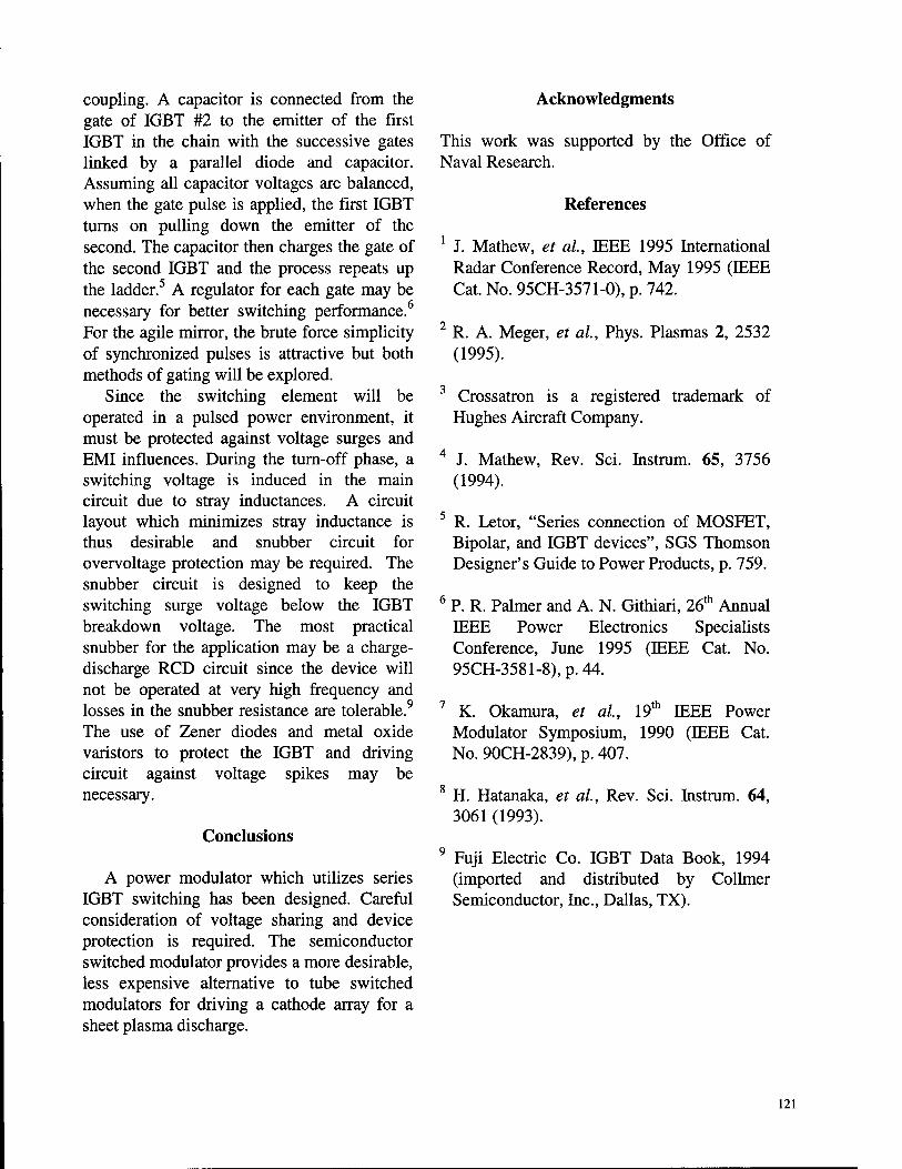
coupling. A capacitor is connected from the gate of IGBT #2 to the emitter of the first IGBT in the chain with the successive gates linked by a parallel diode and capacitor. Assuming all capacitor voltages are balanced, when the gate pulse is applied, the first IGBT turns on pulling down the emitter of the second. The capacitor then charges the gate of the second IGBT and the process repeats up the ladder.5 A regulator for each gate may be necessary for better switching performance.6
For the agile mirror, the brute force simplicity of synchronized pulses is attractive but both methods of gating will be explored.
Since the switching element will be operated in a pulsed power environment, it must be protected against voltage surges and EMI influences. During the turn-off phase, a switching voltage is induced in the main circuit due to stray inductances. A circuit layout which minimizes stray inductance is thus desirable and snubber circuit for overvoltage protection may be required. The snubber circuit is designed to keep the switching surge voltage below the IGBT breakdown voltage. The most practical snubber for the application may be a charge- discharge RCD circuit since the device will not be operated at very high frequency and losses in the snubber resistance are tolerable.9
The use of Zener diodes and metal oxide varistors to protect the IGBT and driving circuit against voltage spikes may be necessary.
Conclusions
A power modulator which utilizes series IGBT switching has been designed. Careful consideration of voltage sharing and device protection is required. The semiconductor switched modulator provides a more desirable, less expensive alternative to tube switched modulators for driving a cathode array for a sheet plasma discharge.
Acknowledgments
This work was supported by the Office of Naval Research.
References
1 J. Mathew, et al, IEEE 1995 International Radar Conference Record, May 1995 (IEEE Cat. No. 95CH-3571-0), p. 742.
2 R. A. Meger, et al, Phys. Plasmas 2, 2532 (1995).
3 Crossatron is a registered trademark of Hughes Aircraft Company.
4 J. Mathew, Rev. Sei. Instrum. 65, 3756 (1994).
5 R. Letor, "Series connection of MOSFET, Bipolar, and IGBT devices", SGS Thomson Designer's Guide to Power Products, p. 759.
6 P. R. Palmer and A. N. Githiari, 26th Annual IEEE Power Electronics Specialists Conference, June 1995 (IEEE Cat. No. 95CH-3581-8),p.44.
7 K. Okamura, et al, 19th IEEE Power Modulator Symposium, 1990 (IEEE Cat. No. 90CH-2839), p. 407.
8 H. Hatanaka, et al, Rev. Sei. Instrum. 64, 3061 (1993).
9 Fuji Electric Co. IGBT Data Book, 1994 (imported and distributed by Collmer Semiconductor, Inc., Dallas, TX).
121
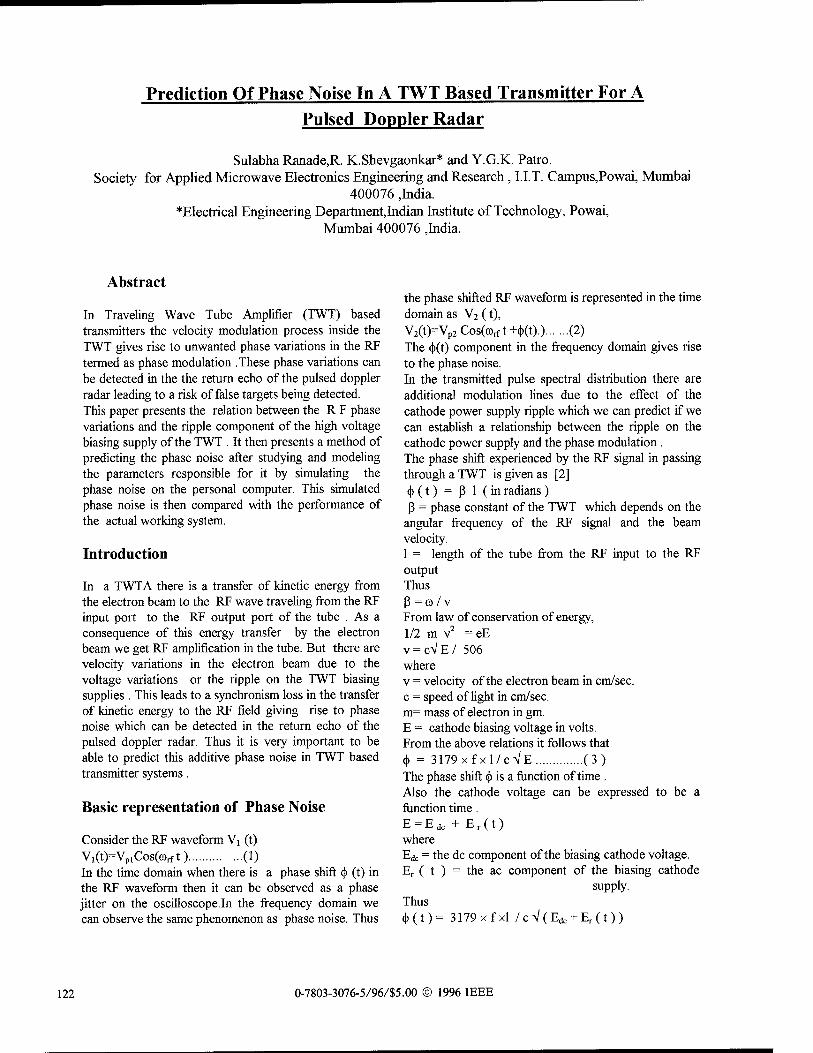
Prediction Of Phase Noise In A TWT Based Transmitter For A Pulsed Doppler Radar
Sulabha Ranade,R. K.Shevgaonkar* and Y.G.K. Patio. Society for Applied Microwave Electronics Engineering and Research, LIT. Campus,Powai, Mumbai
400076 ,India. ♦Electrical Engineering Department,Indian Institute of Technology, Powai,
Mumbai 400076 .India.
Abstract
In Traveling Wave Tube Amplifier (TWT) based transmitters the velocity modulation process inside the TWT gives rise to unwanted phase variations in the RF termed as phase modulation .These phase variations can be detected in the the return echo of the pulsed doppler radar leading to a risk of false targets being detected. This paper presents the relation between the R F phase variations and the ripple component of the high voltage biasing supply of the TWT . It then presents a method of predicting the phase noise after studying and modeling the parameters responsible for it by simulating the phase noise on the personal computer. This simulated phase noise is then compared with the performance of the actual working system.
Introduction
In a TWTA there is a transfer of kinetic energy from the electron beam to the RF wave traveling from the RF input port to the RF output port of the tube . As a consequence of this energy transfer by the electron beam we get RF amplification in the tube. But there are velocity variations in the electron beam due to the voltage variations or the ripple on the TWT biasing supplies . This leads to a synchronism loss in the transfer of kinetic energy to the RF field giving rise to phase noise which can be detected in the return echo of the pulsed doppler radar. Thus it is very important to be able to predict this additive phase noise in TWT based transmitter systems.
Basic representation of Phase Noise
Consider the RF waveform Vi (t) VKtH^CosCmrft) (1) In the time domain when there is a phase shift <J> (t) in the RF waveform then it can be observed as a phase jitter on the oscilloscope.In the frequency domain we can observe the same phenomenon as phase noise. Thus
the phase shifted RF waveform is represented in the time domain as V2 (t), V2(t)=Vp2Cos(arft+<Kt).) (2) The (|)(t) component in the frequency domain gives rise to the phase noise. In the transmitted pulse spectral distribution there are additional modulation lines due to the effect of the cathode power supply ripple which we can predict if we can establish a relationship between the ripple on the cathode power supply and the phase modulation . The phase shift experienced by the RF signal in passing through a TWT is given as [2] <j)(t) = ß 1 (in radians) ß = phase constant of the TWT which depends on the
angular frequency of the RF signal and the beam velocity. 1 = length of the tube from the RF input to the RF output Thus ß = co/v From law of conservation of energy, 1/2 m v2 =eE v = cVE/ 506 where v = velocity of the electron beam in cm/sec. c = speed of light in cm/sec. m= mass of electron in gm. E = cathode biasing voltage in volts. From the above relations it follows that <j) = 3179xfxl/cA/E (3) The phase shift <j> is a function of time . Also the cathode voltage can be expressed to be a function time . E = E dc + E r (t) where Edc = the dc component of the biasing cathode voltage. Er ( t ) = the ac component of the biasing cathode
supply. Thus <()(t)= 3179 xfxl /cV(Edc + Er(t))
122 0-7803-3076-5/96/$5.00 © 1996 IEEE

With appropriate mathematical adjustments <|> (t) = 3179xfxl / c V Edc (l-0.5Er(t)/Edc)
(4) Formulation of the problem
Vi(t).V2(t) = Cos[104 0.00166(Asin ©it+ Asin co2t)] (7)
Implementation of the model
It is now clear that the phase modulation (j)(t) is the root cause of phase noise .Thus we need to model the relationship between the phase modulation (|)(t) and the ac component of the biasing electron beam supply or the cathode supply. If we substitute the derived expression for the phase (p (t) in equation (2) and see V2 (t) in the frequency domain then we could see the modulation lines due to the ripple. The RF signal is in J band and we are analysing the noise in the base band so as to evaluate the signal to interference ratio . So we can bring the carrier to the base band frequency and then take the FFT.We can see the modulation lines on a 512 point FFT . By the analogy of using a mixer as a detector for phase noise measurement in conventional phase noise measurement systems we could multiply the RF signal with the phase shifted RF signal and eliminate the very high frequency components. Multiplying equation 1 and equation 2 and eliminating the high frequency components, V,(t)xV2(t) = Vpl.Vp2Cos(t)(t) LetVpl = Vp2=l Then V!(t)V2(t)=Cos<|>(t) (5) =Cos .[ 3179xfxl / c V Edc (l-.5Er(t)/Edc] Substituting the values of the frequency and length of the tube as given by the tube manufacturers and using c = 3 x 10 10 cm/sec Edc = 30,000V Vi(t).V2(t) = Cos [ 104 -0.00166Er]...( 6 )
Modeling of the ripple
The cathode supply schematic is as shown in figure l.The DC cathode voltage will have two frequency components .The first from the prime power source which is a three phase 400Hz supply and is full wave rectified to give a ripple frequency at 2400Hz.And the second is converter frequency of 125Khz which is full wave rectified to give a ripple frequency of 250Khz. For the present we could consider the capacitive and inductive elements to be only attenuator elements. Consider a simplistic sine wave model for both the ripple components.Then Er(t) is represented as Er(t) = A(sin ©it + sin ro21) with the two ripple frequencies of 2400Hz and 250 Khz. Then
Implementation of the FFT simulation is done using a very user friendly software package called "DSP" used for digital signal processing applications.lt contains blocks which perform various arithmetic , trigonometric as well as FFT functions. The equation (7) is fed into the package with appropriate scaling of frequencies . The figure 2 shows the algorithm of equation (7) with peak to peak ripple of 5 V and figure 3 &4 gives the FFT which represents the phase noise . The results of the actual system are given in figure 5. Figure 5 gives the phase noise of a working TWT based transmitter.
Comparison of the results
The phase noise is represented as the ratio of the single side band power Pssb to the carrier power Pc . For the simulated waveforms Pssb = -58.67 dbc for a ripple of 2400Hz Pc (see fig. 3 )
Pssb = - 57 dbc for a ripple of 250Khz Pc (see fig.4) The phase noise for a working TWT based transmitter with a peak ripple of 5 V is measured as , Pssb= -60dbc/Hz (see fig. 5) Pc
Conclusion
The results of the simulated phase noise show that we can predict the phase noise correctly within a tolerance of 2 to 3 dbc using this simplistic model. We can conclude that modeling of the exact ripple waveform is essential for better prediction .
Acknowledgments
We wish to thank Mr.P.B.Tole and Prof.R.V.S.Sitaram for their continuing support and guidance during the course of our work.My sincere thanks to the entire team of the transmitter project for coordinating to get the requisite results of the TWT based transmitter.
123
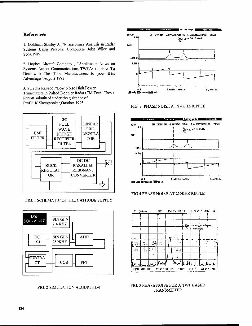
References
1. Goldman Stanley J. /'Phase Noise Analysis in Radar Systems Using Personal Computers."John Wiley and Sons, 1989.
2. Hughes Aircraft Company , "Application Notes on Systems Aspect Communications TWTAs or How To Deal with The Tube Manufacturers to your Best Advantage."August 1982.
3. Sulabha Ranade ,"Low Noise High Power Transmitters in Pulsed Doppler Radars."M.Tech. Thesis Report submitted under the guidance of Prof.R.K.Shevgaonkar, October 1993.
-IBS.8
5.BS8
2 248.3B8 -S.699671B738E*81 i.S7882B2228E»B8 FOLAD Pw - -5C-9 ibc ft
'V A
4=~-
8.8 7.688(10 Hx/Diu H>belp Q>cursoi> gfroxit
6i.443(kj
FIG. 3 PHASE NOISE AT 2.4KHZ RIPPLE
EMI FILTER
3<D FULL
WAVE BRIDGE
RECTIFIER FILTER
LINEAR PRE-
REGULA TOR
BUCK REGULAT
OR
DC-DC PARALLEL RESONANT
CONVERTER
K
^7
2BB 24968.888 -S.8675S49127E«81 2.6i8SB7SS37E»88 KUR
Pist - -5a-Sdbc
y\ v_
Hfrtolp t^cursop lift exit 7.688(h) Hz/»i<i
FIG.4 PHASE NOISE AT 250KHZ RIPPLE
FIG. 1 SCHEMATIC OF THE CATHODE SUPPLY
DSP i SOFTWARE SINGEN
2.4 KHZ
DC 104
G
SINGEN 250KHZ
ADD
SUBTRA r4 CT COS FFT
F" T-BAN» SP: 2kHz/ RL + 0 dBn iOdB/ 3- 1 .... ... |.
1 I 1 ! p_. - **•<( 1 li
1 Mil -Soib /Hx ! ;
: ta":; »'..£-
— i i
! :
•;*& ;- "'i'>. ■■ i'-V ;
■
I \ ' ' i |Uu* *«*•« J/V*-% r*V T J**-r^*<rHj.
• RBW: 300 H z V BW: it 10 Hz SW =: 2 S/ ATT: IOdB
FIG. 2 SIMULATION ALGORITHM FIG. 5 PHASE NOISE FOR A TWT BASED TRANSMITTER
124
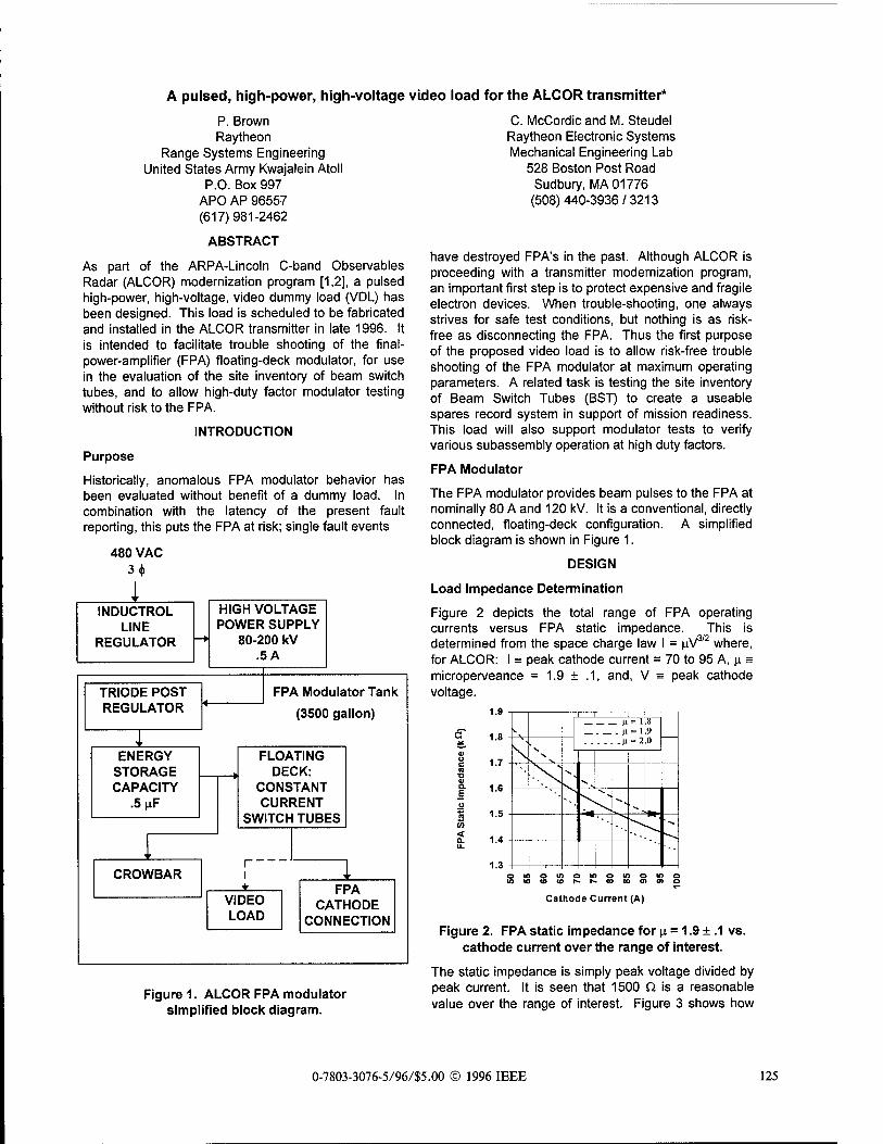
A pulsed, high-power, high-voltage video load for the ALCOR transmitter*
P. Brown Raytheon
Range Systems Engineering United States Army Kwajalein Atoll
P.O. Box 997 APO AP 96557 (617)981-2462
ABSTRACT
As part of the ARPA-Lincoln C-band Observables Radar (ALCOR) modernization program [1,2], a pulsed high-power, high-voltage, video dummy load (VDL) has been designed. This load is scheduled to be fabricated and installed in the ALCOR transmitter in late 1996. It is intended to facilitate trouble shooting of the final- power-amplifier (FPA) floating-deck modulator, for use in the evaluation of the site inventory of beam switch tubes, and to allow high-duty factor modulator testing without risk to the FPA.
INTRODUCTION
Purpose
Historically, anomalous FPA modulator behavior has been evaluated without benefit of a dummy load. In combination with the latency of the present fault reporting, this puts the FPA at risk; single fault events
480 VAC 3 4>
INDUCTROL LINE
REGULATOR
HIGH VOLTAGE POWER SUPPLY
80-200 kV .5 A
TRIODE POST REGULATOR
FPA Modulator Tank
(3500 gallon)
ENERGY STORAGE CAPACITY
.5nF
FLOATING DECK:
CONSTANT CURRENT
SWITCH TUBES
CROWBAR r" i
_*_ VIDEO LOAD
FPA CATHODE
CONNECTION
Figure 1. ALCOR FPA modulator simplified block diagram.
C. McCordic and M. Steudel Raytheon Electronic Systems Mechanical Engineering Lab
528 Boston Post Road Sudbury, MA 01776 (508)440-3936/3213
have destroyed FPA's in the past. Although ALCOR is proceeding with a transmitter modernization program, an important first step is to protect expensive and fragile electron devices. When trouble-shooting, one always strives for safe test conditions, but nothing is as risk- free as disconnecting the FPA. Thus the first purpose of the proposed video load is to allow risk-free trouble shooting of the FPA modulator at maximum operating parameters. A related task is testing the site inventory of Beam Switch Tubes (BST) to create a useable spares record system in support of mission readiness. This load will also support modulator tests to verify various subassembly operation at high duty factors.
FPA Modulator
The FPA modulator provides beam pulses to the FPA at nominally 80 A and 120 kV. It is a conventional, directly connected, floating-deck configuration. A simplified block diagram is shown in Figure 1.
DESIGN
Load Impedance Determination
Figure 2 depicts the total range of FPA currents versus FPA static impedance. determined from the space charge law I for ALCOR: I = peak cathode current = 70 to 95 A, \i = microperveance = 1.9 ± .1, and, V = peak cathode voltage.
operating This is
|iV3/2 where,
\. ji= 1.8 H= 1.9 H = 2.0
s > "-
■v
-.. ■»*
' *» '-■
1 3 -
in ID « w
Cathode Current (A)
Figure 2. FPA static impedance for u = 1.9 + .1 vs. cathode current over the range of interest.
The static impedance is simply peak voltage divided by peak current. It is seen that 1500 Q is a reasonable value over the range of interest. Figure 3 shows how
0-7803-3076-5/96/15.00 © 1996 IEEE 125
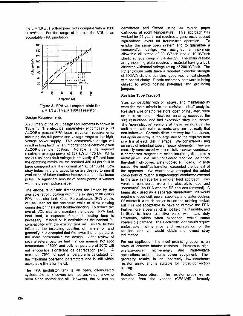
the u = 1.9 ± .1 volt-ampere plots compare with a 1500 Cl resistor. For the range of interest, the VDL is an acceptable FPA simulation.
160
140
120
§ 100
§> 80
o 60
40
20
s,
^ <#i V**
''% s. ?.y
s.t
f r (1=1.8 . .u=1.9 — / H = 2.0
1500 n / 1/ 1 1 I 1 1
Amperes (A)
Figure 3. FPA volt-ampere plots for H = 1.9 + .1 vs. a 1500 Q resistor.
Design Requirements
A summary of the VDL design requirements is shown in Table 1. The electrical parameters encompass all of ALCOR's present FPA beam waveform requirements, including the full power and voltage range of the high- voltage power supply. This conservative design will result in long field life, an important consideration given ALCOR's remote location. Notable is the required maximum average power of 123 kW at 175 kV. While the 200 kV peak fault voltage is not vastly different from the operating maximum, the required 450 kJ per fault is large compared with the nominal of 1 kJ per pulse. Low stray inductance and capacitance are desired to permit evaluation of future risetime improvements in the beam pulse. A significant amount of beam power is wasted with the present pulse shape.
The enclosure outside dimensions are limited by the available retrofit location within the existing 3500 gallon FPA modulator tank. Clear Polycarbonate (PC) plastic will be used for the enclosure walls to allow viewing during design trials and trouble-shooting. To reduce the overall VDL size and maintain the present FPA tank heat load, a separate forced-oil cooling loop is necessary. Mineral oil is desirable as the coolant for compatibility with the existing tank oil. Several factors influence the insulating qualities of mineral oil and generally, it is accepted that the lower the temperature, the more conservative the design. After review of several references, we feel that our nominal hot spot temperature of 50°C and bulk temperature of 30°C will not encourage significant oil degradation [3-5]. A maximum 76°C hot spot temperature is calculated for the maximum operating parameters and is still within acceptable limits for the oil.
The FPA modulator tank is an open, oil-insulated system; the tank covers are not gasketed, allowing room air to contact the oil. However, the oil can be
dehydrated and filtered using 30 micron paper cartridges at room temperature. This approach has worked for 25 years, but requires a generously spaced high-voltage layout for trouble-free operation. To employ the same open system and to guarantee a conservative design, we assigned a maximum allowable oil stress of 20 kV/inch and a 10 kV/inch plastic surface creep in the design. The main resistor array mounting plate requires a material having a bulk dielectric withstand voltage rating of 200 kV/inch. The PC enclosure walls have a reported dielectric strength of 400kV/inch, and combine good mechanical strength with optical clarity. Plastic assembly hardware is being utilized to avoid floating potentials and grounding jumpers.
Resistor Type Tradeoff
Size, compatibility with oil, strays, and maintainability were the main criteria in the resistor tradeoff analysis. Resistive wire or strip resistors, open or insulated, were an attractive option. However, an array exceeded the size restrictions, and had excessive stray inductance. The "non-inductive" versions of these resistors can be fault prone with pulse currents, and are not really that non-inductive. Ceramic disks are very low-inductance, but again an array is too large due to the required heat sink fins at each disk interface. We considered using an array of industrial tubular heater elements. They are coaxially constructed with a resistive center conductor, a compacted magnesium oxide insulating filler, and a metal jacket. We also considered modified use of off- the-shelf high-power, water-cooled RF loads. In both cases, the modification-effort exceeded the benefit of the approach. We would have accepted the added complexity of routing a high-voltage conductor external to the tank in trade for a simpler load approach. Two versions considered were the electrolytic load and "beamstick" (an FPA with the RF sections removed). A beam stick used as a separate stand-alone unit would require a focus coil, power supplies, and water cooling. Of course it is much easier to use the existing socket; but it is not acceptable to have to remove the FPA. Furthermore, a beam stick is not field maintainable, and is likely to have restrictive pulse width and duty limitations, which when exceeded, would cause irreversible damage. The electrolytic load would require undesirable maintenance and recirculation of the solution, and yet would obtain the lowest stray inductance.
For our application, the most promising option is an array of ceramic tubular resistors. Numerous high- average-power, high-energy, and high-voltage applications exist in pulse power equipment. Their geometry results in an inherently low-inductance resistor array, and is suitable for forced-convection cooling.
Resistor Description. The resistor properties as obtained from the vendor (CESIWID, formerly
126
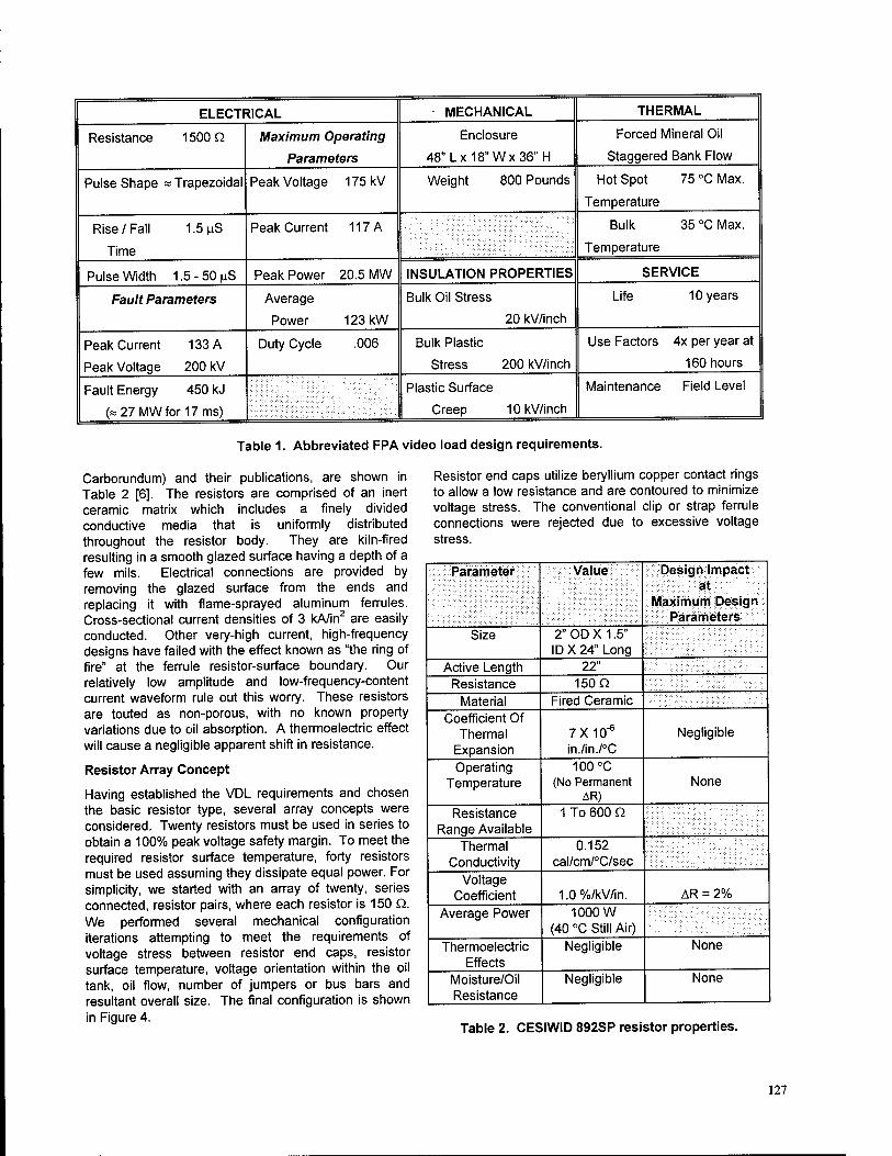
ELECTRICAL MECHANICAL THERMAL
Resistance 1500Q Maximum Operating
Parameters
Enclosure
48"Lx18"Wx36"H
Forced Mineral Oil
Staggered Bank Flow
Pulse Shape « Trapezoidal Peak Voltage 175 kV Weight 800 Pounds Hot Spot 75 °C Max.
Temperature
Rise/Fall 1.5 nS
Time
Peak Current 117A Bulk 35 °C Max.
Temperature
Pulse Width 1.5 - 50 |iS Peak Power 20.5 MW INSULATION PROPERTIES SERVICE
Fault Parameters Average
Power 123 kW
Bulk Oil Stress
20 kV/inch
Life 10 years
Peak Current 133 A
Peak Voltage 200 kV
Duty Cycle .006 Bulk Plastic
Stress 200 kV/inch
Use Factors 4x per year at
160 hours
Fault Energy 450 kJ
(«27MWfor17ms)
Plastic Surface
Creep 10kV/inch
Maintenance Field Level
Table 1. Abbreviated FPA video load design requirements.
Carborundum) and their publications, are shown in Table 2 [6]. The resistors are comprised of an inert ceramic matrix which includes a finely divided conductive media that is uniformly distributed throughout the resistor body. They are kiln-fired resulting in a smooth glazed surface having a depth of a few mils. Electrical connections are provided by removing the glazed surface from the ends and replacing it with flame-sprayed aluminum ferrules. Cross-sectional current densities of 3 kA/in2 are easily conducted. Other very-high current, high-frequency designs have failed with the effect known as "the ring of fire" at the ferrule resistor-surface boundary. Our relatively low amplitude and low-frequency-content current waveform rule out this worry. These resistors are touted as non-porous, with no known property variations due to oil absorption. A thermoelectric effect will cause a negligible apparent shift in resistance.
Resistor Array Concept
Having established the VDL requirements and chosen the basic resistor type, several array concepts were considered. Twenty resistors must be used in series to obtain a 100% peak voltage safety margin. To meet the required resistor surface temperature, forty resistors must be used assuming they dissipate equal power. For simplicity, we started with an array of twenty, series connected, resistor pairs, where each resistor is 150 Q. We performed several mechanical configuration iterations attempting to meet the requirements of voltage stress between resistor end caps, resistor surface temperature, voltage orientation within the oil tank, oil flow, number of jumpers or bus bars and resultant overall size. The final configuration is shown in Figure 4.
Resistor end caps utilize beryllium copper contact rings to allow a low resistance and are contoured to minimize voltage stress. The conventional clip or strap ferrule connections were rejected due to excessive voltage stress.
Parameter Value Design Impact at
Maximum Design Parameters
Size 2" OD X 1.5" ID X 24" Long
Active Length 22" Resistance 150 Q
Material Fired Ceramic Coefficient Of
Thermal Expansion
7X10"6
in./in./°C Negligible
Operating Temperature
100 °C (No Permanent
AR) None
Resistance Range Available
1 To 600 Q
Thermal Conductivity
0.152 cal/cm/°C/sec
Voltage Coefficient 1.0%/kV/in. AR = 2%
Average Power 1000W (40 °C Still Air)
Thermoelectric Effects
Negligible None
Moisture/Oil Resistance
Negligible None
Table 2. CESIWID 892SP resistor properties.
127
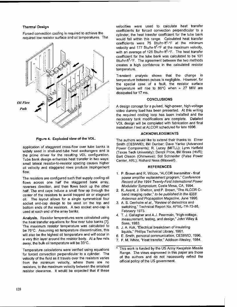
Thermal Design
Forced convection cooling is required to achieve the required low resistor surface and oil temperatures. The
Oil Flow
Path
Figure 4. Exploded view of the VDL.
application of staggered cross-flow over tube banks is widely used in shell-and-tube heat exchangers and is the prime driver for the resulting VDL configuration. Tube bank design enhances heat transfer in two ways: small lateral resistor-to-resistor spacing causes higher oil velocity and staggered rows produce impingement flow.
The resistors are configured such that supply cooling oil flows across one half the staggered bank array, reverses direction, and then flows back up the other half. The end caps induce a small flow up through the center of the resistors to avoid trapped air or stagnant oil. The layout allows for a single symmetrical four socket end-cap design to be used on the top and bottom ends of the resistors. A two socket end-cap is used at each end of the array banks.
Analysis. Resistor temperatures were calculated using the heat transfer equations for flow over tube banks [7]. The maximum resistor temperature was calculated to be 76°C. Assuming no temperature discontinuities, this will also be the highest oil temperature and will occur in a very thin layer around the resistor body. At a few mils away, the bulk oil temperature will be 33°C.
Temperature calculations were verified using equations for forced convection perpendicular to a cylinder. The velocity of the fluid as it travels over the resistors varies from the minimum velocity, where there are no resistors, to the maximum velocity between the smallest resistor clearance. It would be expected that if these
velocities were used to calculate heat transfer coefficients for forced convection perpendicular to a cylinder, the heat transfer coefficient for the tube bank would fall within this range. Calculated heat transfer coefficients were 75 Btu/hr-ft2-°F at the minimum velocity and 177 Btu/hr-ft2-°F at the maximum velocity, with an average of 126 Btu/hr-ft2-°F. The heat transfer coefficient for the tube bank was calculated to be 131 Btu/hr-ft2-°F. The agreement between the two methods creates a high confidence in the calculated resistor temperature.
Transient analysis shows that the change in temperature between pulses is negligible. However, for the special case of a fault, the resistor surface temperature will rise to 86°C when * 27 MW are dissipated for 17 ms.
CONCLUSIONS
A design concept for a pulsed, high-power, high-voltage video dummy load has been presented. At this writing the required cooling loop has been installed and the necessary tank modifications are complete. Detailed VDL design will be completed with fabrication and final installation / test at ALCOR scheduled for late 1996.
ACKNOWLEDGMENTS
The authors would like to extend their thanks to: Elmer Smith (CESIWID); Bill Dunbar; Dave Yanko (Advanced Power Components); R. Lucey (MITLL); Lynn Hatfield (Texas Tech University); Denzil Price, Bill Brass (HVR); Bert Olsson (Ohmweve); Sol Schneider (Pulse Power Center, ARL); Richard Ness (Maxwell).
REFERENCES
1. P. Brown and R. Wilcox, "ALCOR transmitter - final power amplifier replacement program," Conference Record of the 1994 Twenty-First International Power Modulator Symposium, Costa Mesa, CA, 1994.
2. R. Avent, J. Shelton, and P. Brown, "The ALCOR C- band imaging radar," to be published in the IEEE Antennas and Propagation Magazine, June 1996.
3. A. S. Denholm era/., "Review of dielectrics and switching," Technical Report No. AFWL-TR-72-88, February 1973.
4. T. J. Gallagher and A.J. Pearmain, "High-voltage, measurement, testing, and design," John Wiley & Sons, 1983.
5. J. A. Kok, "Electrical breakdown of insulating liquids," Phillips Technical Library, 1961.
6. E. Smith, personal communication, CESIWID, 1996. 7. F. M. White, "Heat transfer," Addison-Wesley, 1984.
* This work is funded by the US Army Kwajalein Missile Range. The views expressed in this paper are those of the authors and do not necessarily reflect the official policy of the US government.
128

Characteristics of Pseudospark Switches for Pulsed Power Modulators
K. Frank, J. Christiansen, S. Döllinger, P. Felsner, A. Görtier, F. Heine, G. Hintz, D.H.H. Hoffmann, U. Prucker, A. Schwandner
University of Erlangen-Nuremberg Physics Department 1, Erwin-Rommel-Str. 1, D-91058 Erlangen, Germany
Abstract
For several years pseudospark switches (PSS) are considered to be an alternative not only to thyratrons or medium-power spark gaps but also to ignitrons. A lifetime of more than 108 discharges with a corresponding total charge transfer of 600 kC was achieved in laser circuits. Electrode erosion is still the main limiting factor to make high power PSS a serious competitor to commercially available switches. One approach to solve this problem is to distribute the total current on several discharge channels with a common hollow cathode. The other one is to look for suitable electrode materials or compounds of them. In order to distribute the discharge homogeneously over more than one single channel synchronous triggering of all channels is indispensable. The trigger method used is a pulsed glow discharge. The characteristics of the trigger discharge as a function of delay and jitter was investigated in combination with actual triggering of all channels. After successful triggering of all channels the corresponding current filaments try to pinch by self-magnetic fields. For long current pulses (i.e. more than 1 or 2 |is for a 80 kA peak current) a single plasma column develops in the symmetry axis of the device. Streak photographs allow to determine pinch time as a function of the peak current, the number of channels, the gap distance and so on. A better understanding of electrode phenomena is essential in order to improve of PSS's to carry high peak currents and simultaneously allow high charge transfer. The critical current density at which electrode erosion dramatically rises is still an unknown parameter.
Introduction like boron carbide or silicon carbide. First experimental results are published in [4].
The pseudospark structure consists of a hollow cathode and hollow anode [1]. The electrodes are cylinders with faces made of refractory metals. The faces of the electrodes have central holes of 3 to 5 mm diameter and are separated by a gap of 3 to 5 mm. These electrodes form an inverted cup structure surrounded by an insulating ceramic tube of a slightly larger diameter. The tube is filled with a gas at low pressure (usually 5 to 80 Pa H2 or D2) and can be triggered by a variety of trigger methods [2]. Electrical breakdown of the gas between the two electrode plates is determined by the product of the gas pressure p and the distance d between the plates. The relation between the (p-d)-product and the breakdown voltage is characterized by PASCHEN'S law. On the basis of the impressive phenomenological properties, a variety of applications [3] developed rapidly. This include, inter alia triggerable high power switches. A new group of high power, low-pressure "thyratron-type" switches has been developed for high frequency and high current pulsed power applications. The current stage of development is summarized in Table 1. By use of pure tungsten electrodes a 600 kC total charge transfer has been demonstrated (by courtesy of Siemens AG Corporate Research, Erlangen). To achieve longer lifetimes there are two options: The first is to share out the total discharge current between several discharge channels by multichannel configuration. The second is to try to diffuse the discharge plasma over a larger electrode surface. This can be achieved by using inserts of semiconductor material
State-of-the-art * these numbers have been achieved for different discharge parameters
medium power
high power high voltage
one gap one channel
one gap one channel
one gap three channel coaxial
one gap three channel radial
three gaps one channel
type sealed off modular o-ring sealed o-ring sealed o-rine sealed anode voltase 32 kV 30 kV 20 kV 20 kV 65 kV anode current 30 kA 120kA 60 kA 240 kA 18kA
reverse current
100%
current rise 8-10" A/s 1.5-10" A/s 2-10" A/s 1.8-10" A/s 7-10'" A/s
charge per pulse
0.015 C 1.8 C 0.1 C 3.4 C 0.05 C
max. pulse length
500 ns 2.5 us lus 10 us < 500 ns
delay 100 - 600 ns < 500 ns 300 ns 500 ns 170 ns jitter 5ns (600 ps*) 40 ns <5 ns 15 ns 30 ns pulse
repetition rate
1.8 kHz 0.3 Hz 0.5 Hz - lifetime 1.2-10*
pulses* 10 pulses* - 2.5-104 pulses -
total charge transfer
220 kC* 27 kC* - 50 kC*
Table 1: Current stage of development of high power pseudospark switches. The tube data lists in the first column ("medium power") correspond to numbers of a PSS constructed according to the rules of modern tube technology. These PSS are commercially available, too. The other PSS types are still in the stage of development. This especially applies for the high voltage device.
0-7803-3076-5/96/S5.00 © 1996 IEEE 129
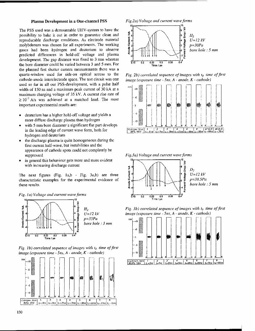
Plasma Development in a One-channel PSS
The PSS used was a demountable UHV-system to have the possibility to bake it out in order to guarantee clean and reproducable discharge conditions. As electrode material molybdenum was chosen for all experiments. The working gases had been hydrogen and deuterium to observe predicted differences in hold-off voltage and plasma development. The gap distance was fixed to 3 mm whereas the bore diameter could be varied between 3 and 5 mm. For the planned fast shutter camera measurements there was a quartz-window used for side-on optical access to the cathode-anode interelectrode space. The test circuit was one used so far in all our PSS-development, with a pulse half width of 150 ns and a maximum peak current of 30 kA at a maximum charging voltage of 35 kV. A current rise rate of > 10" A/s was achieved at a matched load. The most important experimental results are:
• deuterium has a higher hold-off voltage and yields a more diffuse discharge plasma than hydrogen
• with 5 mm bore diameter a significant flat part develops in the leading edge of current wave form, both for hydrogen and deuterium
• the discharge plasma is quite homogeneous during the first current half-wave, but instabilities and the appearance of cathode spots could not completely be suppressed
• in general this behaviour gets more and more evident with increasing discharge current
The next figures (Fig. la,b - Fig. 3a,b) are three characteristic examples for the experimental evidence of these results.
Fig. la) Voltage and current waveforms 12__^- ,12
Fig.2a) Voltage and current waveforms
8 4
?o •a o c < -4
V \ \
X.
1 23 45 57 8
H7 4| U=12kV 0| p=35Pa
'S bore hole : 3 mm
3.15 0.2 0.25 0.3 0.35 0.4 Time / MS
Fig. lb) correlated sequence of images with t0 time of first image (exposure time - 5ns, A - anode, K - cathode)
K Al JK Al « A. IK Al JK Hydrogen. 3mm '• ?■ 3. * 6". 6. ] 7.
35Pä. 13kV latins fo*&rs t.j + 21ns l0*31rts tc + 36ns t0 + 52ns fa + 61ns
H2
U=12kV p=30Pa bore hole : 5 mm
Fig. 2b) correlated sequence of images with t0 time of first image (exposure time - 5ns, A - anode, K - cathode)
K Al K A JK h- JK AL K A! IK Al Hydrogen. 5mm | T ] 2 \ 3 4 S f « T e7 (S.4) eS (5,4)
30P3, WW I fa» 0ns I /<. * 7ns I fe > 19m\ t, + 31ns\ le + 40t>$] f» + 59ns\ to * 69ns\ te* 78ns'
Fig.3a) Voltage and current waveforms
D2
U=12kV p=38.5Pa bore hole : 5 mm
Fig. 3b) correlated sequence of images with t0 time of first image (exposure time - 5ns, A - anode, K - cathode)
I »
Deuterium. 5mm 1 2 3 4 5 6 7 ü \ 38.5Pä. KkV I h -0ns I tttSns I Im-JWris I hfiSns I l.^3Bns I foSSns | !^7Sr.s \ l„+102ns.
130
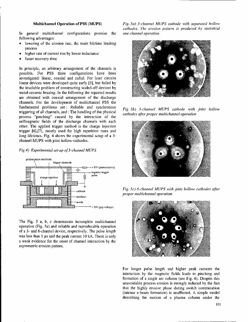
Multichannel Operation of PSS (MUPS)
In general multichannel configurations promise the following advantages: • lowering of the erosion rate, the main lifetime limiting
process • higher rate of current rise by lower inductance • faster recovery time
In principle, an arbitrary arrangement of the channels is possible. For PSS three configurations have been investigated: linear, coaxial and radial. For laser circuits linear devices were developed quite early [5], but failed by the insoluble problem of constructing sealed-off devices by metal-ceramic brazing. In the following the reported results are obtained with coaxial arrangement of the discharge channels. For the development of multichannel PSS the fundamental problems are: Reliable and synchronous triggering of all channels, and : The handling of the physical process "pinching" caused by the interaction of the selfmagnetic fields of the discharge channels with each other. The applied trigger method is the charge injection trigger [6],[7], mostly used for high repetition rates and long lifetimes. Fig. 4 shows the experimental setup of a 3- channel MUPS with joint hollow-cathodes.
Fig.4) Experimental set-up of3-channel MUPS
preionization electrode \ , trigger electrode
KZJ—« + HV (preionization)
■-. negative trigger pulse
- HV (gap voltage)
The Fig. 5 a, b, c demonstrate incomplete multichannel operation (Fig. 5a) and reliable and reproducable operation of a 3- and 6-channel device, respectively. The pulse length was less than 1 us and the peak current 10 kA. There is only a weak evidence for the onset of channel interaction by the asymmetric erosion pattern.
Fig. 5a) 3-channel MUPS cathode with separated hollow cathodes. The erosion pattern is produced by statistical one-channel operation
Fig. 5b) 3-channel MUPS cathode with joint hollow cathodes after proper multichannel operation
Fig. 5c) 6-channel MUPS with joint hollow cathodes after proper multichannel operation
. »*Oj
For longer pulse length and higher peak currents the interaction by the magnetic fields leads to pinching and formation of a single arc column (see Fig. 6). Despite this unavoidable process erosion is strongly reduced by the fact that the highly erosive phase during switch commutation (intense e-beam formation) is unaffected. A simple model describing the motion of a plasma column under the
131
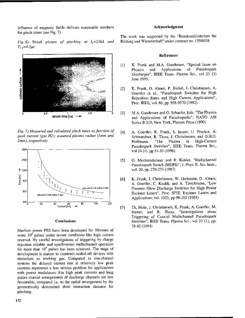
influence of magnetic fields delivers reasonable numbers for pinch times (see Fig. 7).
Fig. 6) Streak picture of pinching at Ip=25kA and Tn2=4.5ps
Acknowledgment
The work was supported by the "Bundesministerium für Bildung und Wissenschaft" under contract no. 13N6038
0.5 1 streak time [tisj
Fig. 7) Measured and calculated pinch times as function of peak current (gas H2); assumed plasma radius (1mm and 2mm), respectively
1800
1500
1200
900
600
300
calculated with radius 2 mm
calculated with radius 1 mm
20 40 60 80 Current [kA] -*-
Conclusions
100 120
Medium power PSS have been developed for lifetimes of some 108 pulses under severe conditions like high current reversal. By careful investigations of triggering by charge injection reliable and synchronous multichannel operation for more than 106 pulses has been achieved. The stage of development is mature to construct sealed-off devices with deuterium as working gas. Compared to one-channel systems the delayed current rise at relatively low peak currents represents a less serious problem for applications with power modulators. For high peak currents and long pulses coaxial arrangements of discharge channels are less favourable, compared i.e. to the radial arrangement by the geometrically determined short interaction distance for pinching.
References
[1] K. Frank and M.A. Gundersen, "Special Issue on Physics and Applications of Pseudospark Discharges", IEEE Trans. Plasma Sei., vol 23 (3) June 1995.
[2] K. Frank, O. Almen, P. Bickel, J. Christiansen, A. Goertler et al., "Pseudospark Switches for High Repetition Rates and High Current Applications", Proc. IEEE, vol. 80, pp. 958-9570 (1992).
[3] M.A. Gundersen and G. Schaefer, Eds. "The Physics and Applications of Pseudosparks", NATO ASI Series B 219, New York, Plenum Press (1990)
[4] A. Goertler, K. Frank, S. Insam, U. Prucker, A. Schwandner, R. Tkotz, J. Christiansen, and D.H.H. Hoffmann, "The Plasma in High-Current Pseudospark Switches", IEEE Trans. Plasma Sei., vol 24 (1), pp 51-53 (1996)
[5] G. Mechtersheimer and R. Köhler, "Multichannel Pseudospark Switch (MUPS)", J. Phys. E. Sei. Instr., vol. 20, pp. 270-273 (1987)
[6] K. Frank, J. Christiansen, W. Hartmann, O. Almen, A. Goertler, C. Kozlik, and A. Tinschmann, "Low Pressure Glow Discharge Switches for High Power Excimer Lasers", Proc. SPIE, Excimer Lasers and Applications, vol. 1023, pp 98-102 (1988)
[7] Th. Mehr, J. Christiansen, K. Frank, A. Goertler, M. Stetter, and R. Tkotz, "Investigations about Triggering of Coaxial Multichannel Pseudospark Switches", IEEE Trans. Plasma Sei., vol 22 (1), pp. 78-82 (1994)
132
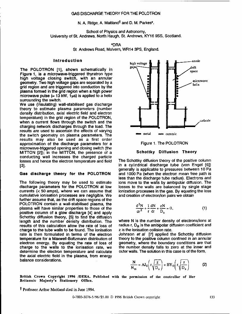
GAS DISCHARGE THEORY FOR THE POLOTRON
N. A. Ridge, A. Maitland* and D. M. Parkes*.
School of Physics and Astronomy, University of St. Andrews, North Haugh, St. Andrews, KY16 9SS, Scotland.
*DRA St Andrews Road, Malvern, WR14 3PS, England.
Introduction
The POLOTRON [1], shown schematically in Figure 1, is a microwave-triggered thyratron type high voltage closing switch, with an annular geometry. Two high voltage gaps are separated by a grid region and are triggered into conduction by the plasma formed in the grid region when a high power microwave pulse (-13 kW, 1 us) is applied to a helix surrounding the switch. We use (insulating) wall-stabilised gas discharge theory to estimate plasma parameters (number density distribution, axial electric field and electron temperature) in the grid region of the POLOTRON, when a current flows through the switch and the charging network discharges through the load. The results are used to ascertain the effects of varying the switch geometry on plasma parameters. The results may also be used as a first order approximation of the discharge parameters for a microwave-triggered opening and closing switch (the MITTON [2]); in the MITTON, the presence of a conducting wall increases the charged particle losses and hence the electron temperature and field [3].
Gas discharge theory for the POLOTRON
The following theory may be used to estimate discharge parameters for the POLOTRON at low currents (< 50 amps), where we can assume that cumulative ionisation processes are negligible. We further assume that, as the drift space regions of the POLOTRON contain a wall-stabilised plasma, the plasma will have similar properties to those of the positive column of a glow discharge [4] and apply Schottky diffusion theory, [5] to find the diffusion length and the number density distribution. The results of this calculation allow the rate of loss of charge to the tube walls to be found. The ionisation rate is then formulated in terms of the electron temperature for a Maxwell-Boltzmann distribution of electron energy. By equating the rate of loss of charge to the walls to the ionisation rate, we determine the electron temperature and calculate the axial electric field in the plasma, from energy balance considerations.
high voltage gaps,
anode
cathode
metal *>*»* ceramic
Figure 1. The POLOTRON
Schottky Diffusion Theory
The Schottky diffusion theory of the positive column in a cylindrical discharge tube (von Engel [6]) generally is applicable to pressures between 10 Pa and 1000 Pa (when the electron mean free path is less than the discharge tube radius). Electrons and ions move to the walls by ambipolar diffusion. The losses to the walls are balanced by single stage ionization processes in the gas. By equating the loss and creation of electron/ion pairs we obtain
d2N dr2
1 dN zN _ + r dr + D " ' (1)
where N is the number density of electrons/ions at radius r, Da is the ambipolar diffusion coefficient and z is the ionisation collision rate. Johnson et al [7] applied the Schottky diffusion theory to the positive column confined in an annular geometry, where the boundary conditions are that the number density falls to zero at the inner and outer walls. The solution in this case is of the form,
^ (2)
British Crown Copyright 1996 /DERA. Published with the permission of the controller of Her Britannic Majesty's Stationery Office.
t Professor Arthur Maitland died in June 1994.
0-7803-3076-5/96/S5.00 © 1996 British Crown copyright 133
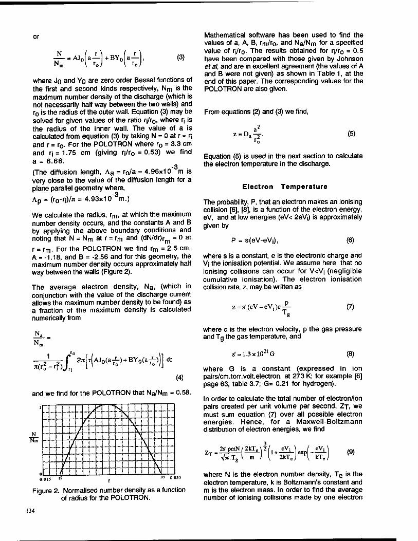
or
N
Nm
AJf a—]+BY0fa T (3)
where Jo and Yo are zero order Bessel functions of the first and second kinds respectively, Nm is the maximum number density of the discharge (which is not necessarily half way between the two walls) and r0 is the radius of the outer wall. Equation (3) may be solved for given values of the ratio n/r0, where n is the radius of the inner wall. The value of a is calculated from equation (3) by taking N = 0 at r = r; and r = r0. For the POLOTRON where r0 = 3.3 cm and n = 1.75 cm (giving rj/r0 = 0.53) we find a = 6.66. (The diffusion length, Aa = »o/a = 4.96x10"3m is very close to the value of the diffusion length for a plane parallel geometry where,
Ap = (r0-n)/jt = 4.93x10" m.)
We calculate the radius, rm, at which the maximum number density occurs, and the constants A and B by applying the above boundary conditions and noting that N = Nm at r = rm and (dN/dr)rm = 0 at r = rm. For the POLOTRON we find rm = 2.5 cm, A = -1.18, and B = -2.56 and for this geometry, the maximum number density occurs approximately half way between the walls (Figure 2).
The average electron density, Na, (which in conjunction with the value of the discharge current allows the maximum number density to be found) as a fraction of the maximum density is calculated numerically from
2k = Nm
1_r%Jr(AJ0(a^) + BY0(a^))] dr n(ro-ri )Jrj L J
(4)
and we find for the POLOTRON that Na/Nm = 0.58.
1
,-~ | T~ : —. j™
N t™
..... .... ....
:
0 0.015 ri ro 0.035
Figure 2. Normalised number density as a function of radius for the POLOTRON.
Mathematical software has been used to find the values of a, A, B, rm/r0, and Na/Nm for a specified value of rj/ro- The results obtained for rj/ro = 0.5 have been compared with those given by Johnson et al, and are in excellent agreement (the values of A and B were not given) as shown in Table 1, at the end of this paper. The corresponding values for the POLOTRON are also given.
From equations (2) and (3) we find,
„2 D »2
'o (5)
Equation (5) is used in the next section to calculate the electron temperature in the discharge.
Electron Temperature
The probability, P, that an electron makes an ionising collision [6], [8], is a function of the electron energy, eV, and at low energies (eV< 2eVj) is approximately given by
P = s(eV-eVj), (6)
where s is a constant, e is the electronic charge and Vj the ionisation potential. We assume here that no ionising collisions can occur for V<Vj (negligible cumulative ionisation). The electron ionisation collision rate, z, may be written as
z = s'(eV-eVi)c-^ (7)
where c is the electron velocity, p the gas pressure and Tg the gas temperature, and
:1.3xl021G (8)
where G is a constant (expressed in ion pairs/cm.torr.volt.electron, at 273 K; for example [6] page 63, table 3.7; G= 0.21 for hydrogen).
In order to calculate the total number of electron/ion pairs created per unit volume per second, Zj, we must sum equation (7) over all possible electron energies. Hence, for a Maxwell-Boltzmann distribution of electron energies, we find
^m^)> eVj 2kT„
exp - eV; kT„ (9)
where N is the electron number density, Te is the electron temperature, k is Boltzmann's constant and m is the electron mass. In order to find the average number of ionising collisions made by one electron
134
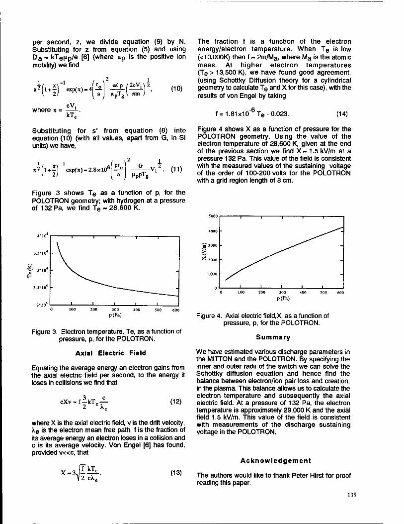
per second, z, we divide equation (9) by N. Substituting for z from equation (5) and using Da - kTenp/e [6] (where \ip is the positive ion mobility) we find
■'K)" «*>-^J vffl1- (10)
eV; where x = kT,
Substituting for s' from equation (8) into equation (10) (with all values, apart from G, in SI units) we have,
12/ n [ a J HppTg V- (11)
Figure 3 shows Te as a function of p, for the POLOTRON geometry; with hydrogen at a pressure of 132 Pa, we find Te - 28,600 K.
Figure 3. Electron temperature, Te, as a function of pressure, p, for the POLOTRON.
Axial Electric Field
Equating the average energy an electron gains from the axial electric field per second, to the energy it loses in collisions we find that,
eXv-f-kT„ — (12)
where X is the axial electric field, v is the drift velocity, \e is the electron mean free path, f is the fraction of its average energy an electron loses in a collision and c is its average velocity. Von Engel [6] has found, provided v«c, that
■4 kTe (13)
The fraction f is a function of the electron energy/electron temperature. When Te is low (<10,000K) then f - 2m/Ma, where Ma is the atomic mass. At higher electron temperatures (Te > 13,500 K), we have found good agreement, (using Schottky Diffusion theory for a cylindrical geometry to calculate Te and X for this case), with the results of von Engel by taking
f = 1.81x10 Te-0.023. (14)
Figure 4 shows X as a function of pressure for the POLOTRON geometry. Using the value of the electron temperature of 28,600 K, given at the end of the previous section we find X - 1.5 kV/m at a pressure 132 Pa. This value of the field is consistent with the measured values of the sustaining voltage of the order of 100-200 volts for the POLOTRON with a grid region length of 8 cm.
4000
T 1 1 "1 1
'S*3000 ^^""^
* 2000 -
1000
a ' I " ' 300
p(Pa)
Figure 4. Axial electric field.X, as a function of pressure, p, for the POLOTRON.
Summary
We have estimated various discharge parameters in the MITTON and the POLOTRON. By specifying the inner and outer radii of the switch we can solve the Schottky diffusion equation and hence find the balance between electron/ion pair loss and creation, in the plasma. This balance allows us to calculate the electron temperature and subsequently the axial electric field. At a pressure of 132 Pa, the electron temperature is approximately 29,000 K and the axial field 1.5 kV/m. This value of the field is consistent with measurements of the discharge sustaining voltage in the POLOTRON.
Acknowledgement
The authors would like to thank Peter Hirst for proof reading this paper.
135
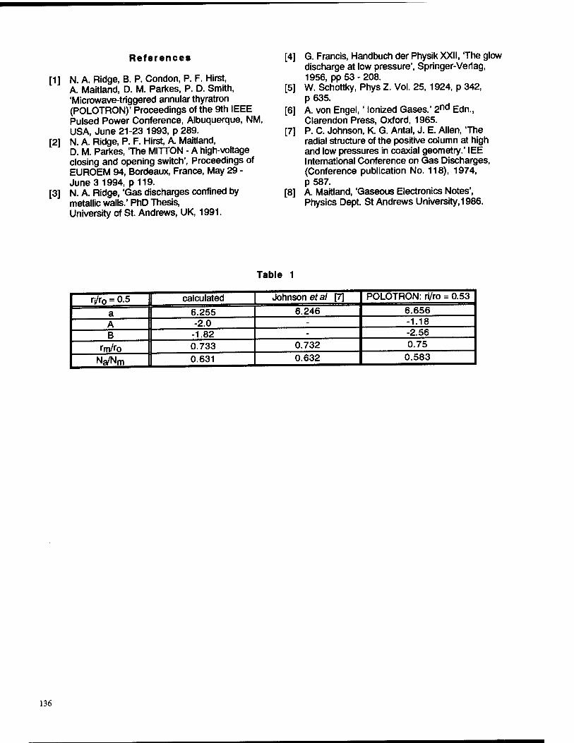
[1]
[2]
[3]
References [4]
N. A. Ridge, B. P. Condon, P. F. Hirst, A. Maitland, D. M. Parkes, P. D. Smith, [5] 'Microwave-triggered annular thyratron (POLOTRON)' Proceedings of the 9th IEEE [6] Pulsed Power Conference, Albuquerque, NM, USA, June 21-23 1993, p 289. [7] N. A. Ridge, P. F. Hirst, A Maitland, D. M. Parkes, The MITTON - A high-voltage closing and opening switch', Proceedings of EUROEM 94, Bordeaux, France, May 29 - June 3 1994, p119. N. A. Ridge, 'Gas discharges confined by [8] metallic walls.' PhD Thesis, University of St. Andrews, UK, 1991.
G. Francis, Handbuch der Physik XXII, 'The glow discharge at low pressure', Springer-Verlag, 1956, pp53-208. W. Schottky, Phys Z. Vol. 25, 1924, p 342, p635. A. von Engel,' Ionized Gases.' 2nd Edn., Clarendon Press, Oxford, 1965. P. C. Johnson, K. G. Antal, J. E. Allen, 'The radial structure of the positive column at high and low pressures in coaxial geometry.' IEE International Conference on Gas Discharges, (Conference publication No. 118), 1974, p587. A. Maitland, 'Gaseous Electronics Notes', Physics Dept. St Andrews University, 1986.
Table 1
rj/r0 = 0.5 calculated Johnson era/ [7] POLOTRON: ri/ro = 0.53
a 6.255 6.246 6.656
A -2.0 - -1.18
B -1.82 - -2.56
imAo 0.733 0.732 0.75
Na/Nm 0.631 0.632 0.583
136
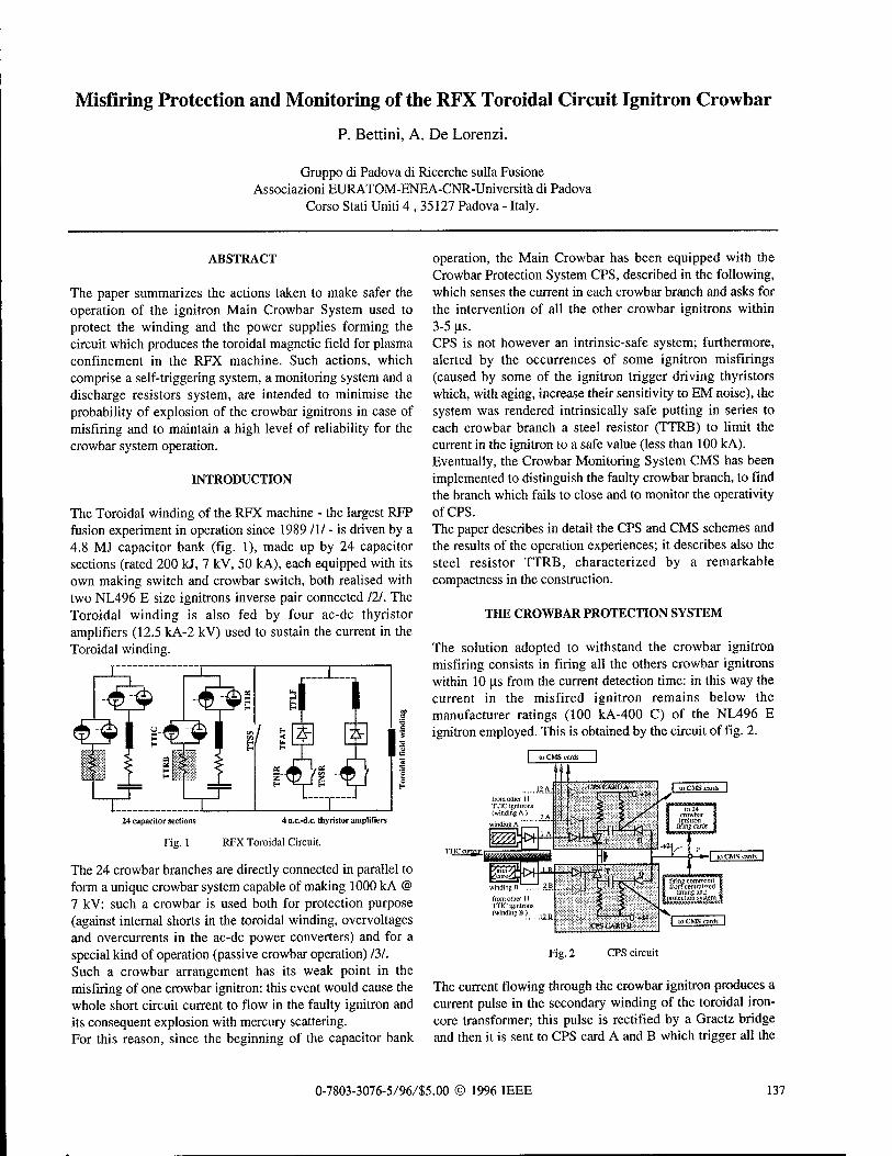
Misfiring Protection and Monitoring of the RFX Toroidal Circuit Ignitron Crowbar
P. Bettini, A. De Lorenzi.
Gruppo di Padova di Ricerche sulla Fusione Associazioni EURATOM-ENEA-CNR-Universitä di Padova
Corso Stati Uniti 4 , 35127 Padova - Italy.
ABSTRACT
The paper summarizes the actions taken to make safer the operation of the ignitron Main Crowbar System used to protect the winding and the power supplies forming the circuit which produces the toroidal magnetic field for plasma confinement in the RFX machine. Such actions, which comprise a self-triggering system, a monitoring system and a discharge resistors system, are intended to minimise the probability of explosion of the crowbar ignitrons in case of misfiring and to maintain a high level of reliability for the crowbar system operation.
INTRODUCTION
The Toroidal winding of the RFX machine - the largest RFP fusion experiment in operation since 1989 III - is driven by a 4.8 MJ capacitor bank (fig. 1), made up by 24 capacitor sections (rated 200 kJ, 7 kV, 50 kA), each equipped with its own making switch and crowbar switch, both realised with two NL496 E size ignitrons inverse pair connected 111. The Toroidal winding is also fed by four ac-dc thyristor amplifiers (12.5 kA-2 kV) used to sustain the current in the Toroidal winding.
24 capacitor sections
Fig. 1
4 a.c.-d.c. thyristor amplifiers
RFX Toroidal Circuit.
The 24 crowbar branches are directly connected in parallel to form a unique crowbar system capable of making 1000 kA @ 7 kV: such a crowbar is used both for protection purpose (against internal shorts in the toroidal winding, overvoltages and overcurrents in the ac-dc power converters) and for a special kind of operation (passive crowbar operation) 131. Such a crowbar arrangement has its weak point in the misfiring of one crowbar ignitron: this event would cause the whole short circuit current to flow in the faulty ignitron and its consequent explosion with mercury scattering. For this reason, since the beginning of the capacitor bank
operation, the Main Crowbar has been equipped with the Crowbar Protection System CPS, described in the following, which senses the current in each crowbar branch and asks for the intervention of all the other crowbar ignitrons within 3-5 us. CPS is not however an intrinsic-safe system; furthermore, alerted by the occurrences of some ignitron misfirings (caused by some of the ignitron trigger driving thyristors which, with aging, increase their sensitivity to EM noise), the system was rendered intrinsically safe putting in series to each crowbar branch a steel resistor (TTRB) to limit the current in the ignitron to a safe value (less than 100 kA). Eventually, the Crowbar Monitoring System CMS has been implemented to distinguish the faulty crowbar branch, to find the branch which fails to close and to monitor the operativity of CPS. The paper describes in detail the CPS and CMS schemes and the results of the operation experiences; it describes also the steel resistor TTRB, characterized by a remarkable compactness in the construction.
THE CROWBAR PROTECTION SYSTEM
The solution adopted to withstand the crowbar ignitron misfiring consists in firing all the others crowbar ignitrons within 10 us from the current detection time: in this way the current in the misfired ignitron remains below the manufacturer ratings (100 kA-400 C) of the NL496 E ignitron employed. This is obtained by the circuit of fig. 2.
(winding B )
Fig. 2 CPS circuit
The current flowing through the crowbar ignitron produces a current pulse in the secondary winding of the toroidal iron- core transformer; this pulse is rectified by a Graetz bridge and then it is sent to CPS card A and B which trigger all the
0-7803-3076-5/96/S5.00 © 1996 IEEE 137
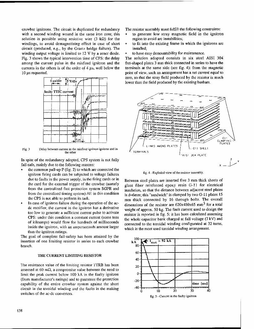
crowbar ignitrons. The circuit is duplicated for redundancy with a second winding wound in the same iron core; this solution is possible using resistive wire (3 k£2) for the windings, to avoid demagnetising effect in case of short circuit (produced, e.g., by the Graetz bridge failure). The winding output voltage is limited to 12 V by a zener diode. Fig. 3 shows the typical intervention time of CPS: the delay among the current pulse in the misfired ignitron and the currents in the others is of the order of 4 us, well below the 10 us requested.
Fig. 3 Delay between current in the misfired ignitron ignitron and in the other
In spite of the redundancy adopted, CPS system is not fully fail-safe, mainly due to the following reasons: • the common pull-up P (fig. 2) to which are connected the
ignitron firing cards can be subjected to voltage failures due to faults in the power supply, in the firing cards or in the card for the external trigger of the crowbar (namely from the centralized fast protection system SGPR and from the centralized timing system) 141: in this condition the CPS is not able to perform its task.
• In case of ignitron failure during the operation of the ac- dc rectifier, the current in the ignitron has a derivative too low to generate a sufficient current pulse to activate CPS: under this condition a constant current (some tens of kiloamps) would flow for hundreds of milliseconds inside the ignitron, with an amperseconds amount larger than the ignitron ratings.
The goal of complete fail-safety has been attained by the insertion of one limiting resistor in series to each crowbar branch.
THE CURRENT LIMITING RESISTOR
The resistance value of the limiting resistor TTRB has been assessed at 60 mQ, a compromise value between the need to limit the peak current below 100 kA in the faulty ignitron (from manufacturer's ratings) and to guarantee the protection capability of the entire crowbar system against the short circuit in the toroidal winding and the faults in the making switches of the ac-dc converters.
The resistor assembly must fulfill the following constraints: • to generate low stray magnetic field in the ignitron
region to avoid arc instabilities; • to fit into the existing frame in which the ignitrons are
installed; • to have easy demountability for maintenance. The solution adopted consists in six steel AISI 304 fret-shaped plates 3 mm thick connected in series to have the terminals at the same side (see fig. 4): from the magnetic point of view, such an arrangement has a net current equal to zero, so that the stray field produced by the resistor is much lower than the field produced by the existing busbars.
G1 1 CLAMPING PLATES
G11 SHEET
AISI 304 PLATE
fig. 4 - Exploded view of the resistor assembly.
Between steel plates are inserted five 3 mm thick sheets of glass fiber reinforced epoxy resin G-ll for electrical insulation, so that the distance between adjacent steel plates is d=6mm; this "sandwich" is clamped by two G-ll plates 15 mm thick connected by 16 through bolts. The overall dimensions of the resistor are 620x480x65 mm^ for a total weight of approx. 50 kg. The fault current used to design the resistor is reported in fig. 5: it has been calculated assuming the whole capacitor bank charged at full voltage (7 kV) and connected to the toroidal winding configurated at 32 turns, which is the most used toroidal winding arrangement.
100- kA
80-
60-
40'
20-
-20-
-40-
:V<IMAx = 92kA
: \
\
\
\
\ ^ y^ ; time [ms]
10 20 30 40
fig. 5 - Current in the faulty ignitron
138
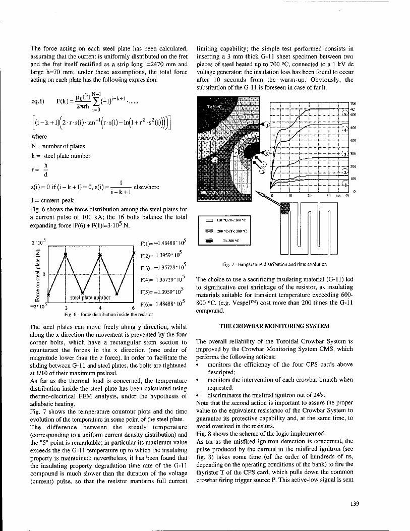
The force acting on each steel plate has been calculated, assuming that the current is uniformly distributed on the fret and the fret itself rectified as a strip long 1=2470 mm and large h=70 mm; under these assumptions, the total force acting on each plate has the following expression:
eq.l) ,, T21 N_1
F(k) = HöLLX(-1)i_k+1' 27trh 1 i=0
(i-k + l/2-r-s(i)-tan_1(r-s(i)-ln(l + r2-s2(i)))
where
N = number of plates
k = steel plate number
h r = —
d
s(i) = 0if(i-k + l) = 0,s(i): elsewhere i-k + 1
I = current peak Fig. 6 shows the force distribution among the steel plates for a current pulse of 100 kA; the 16 bolts balance the total expanding force IF(6)I+IF(1)I=3-105 N.
2'10" F(l)= 1.48488" 105
-2*10
F(2)= 1.3959-10
F(3)=-1.35729-105
F(4)= 1.35729-105
F(5)= -1.3959" 105
F(6)= 1.48488 MO5
Fig. 6 - force distribution inside the resistor
The steel plates can move freely along y direction, whilst along the x direction the movement is prevented by the four corner bolts, which have a rectangular stem section to counteract the forces in the x direction (one order of magnitude lower than the z force). In order to facilitate the sliding between G-l 1 and steel plates, the bolts are tightened at 1/10 of their maximum preload. As far as the thermal load is concerned, the temperature distribution inside the steel plate has been calculated using thermo-electrical FEM analysis, under the hypothesis of adiabatic heating. Fig. 7 shows the temperature countour plots and the time evolution of the temperature in some point of the steel plate. The difference between the steady temperature (corresponding to a uniform current density distribution) and the "5" point is remarkable; in particular its maximum value exceeds the the G-ll temperature up to which the insulating property is maintained; nevertheless, it has been found that the insulating property degradation time rate of the G-ll compound is much slower than the duration of the voltage (current) pulse, so that the resistor mantains full current
limiting capability; the simple test performed consists in inserting a 3 mm thick G-ll sheet specimen between two pieces of steel heated up to 700 °C, connected to a 1 kV dc voltage generator: the insulation loss has been found to occur after 10 seconds from the warm-up. Obviously, the substitution of the G-ll is foreseen in case of fault.
EZ1 150 -C<T< 200 'C
liäiiijj 200 'C<T< 300 -C
mm T>300-C
Fig. 7 - temperature distribution and time evolution
The choice to use a sacrificing insulating material (G-ll) led to significative cost shrinkage of the resistor, as insulating materials suitable for transient temperature exceeding 600- 800 °C. (e.g. Vespel™) cost more than 200 times the G-l 1 compound.
THE CROWBAR MONITORING SYSTEM
The overall reliability of the Toroidal Crowbar System is improved by the Crowbar Monitoring System CMS, which performs the following actions: • monitors the efficiency of the four CPS cards above
descripted; • monitors the intervention of each crowbar branch when
requested; • discriminates the misfired ignitron out of 24's. Note that the second action is important to assure the proper value to the equivalent resistance of the Crowbar System to guarantee its protective capability and, at the same time, to avoid overload in the resistors. Fig. 8 shows the scheme of the logic implemented. As far as the misfired ignitron detection is concerned, the pulse produced by the current in the misfired ignitron (see fig. 3) takes some time (of the order of hundreds of ns, depending on the operating conditions of the bank) to fire the thyristor T of the CPS card, which pulls down the common crowbar firing trigger source P. This active-low signal is sent
139
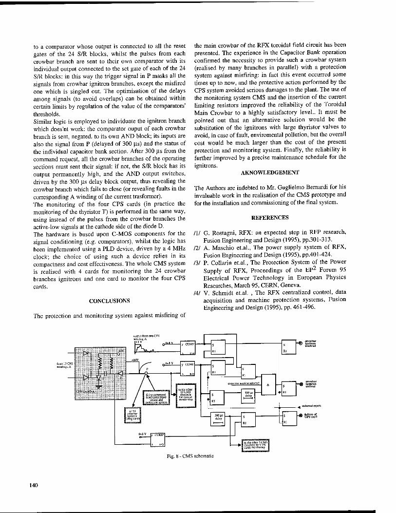
to a comparator whose output is connected to all the reset gates of the 24 S/R blocks, whilst the pulses from each crowbar branch are sent to their own comparator with its individual output connected to the set gate of each of the 24 S/R blocks: in this way the trigger signal in P masks all the signals from crowbar ignitron branches, except the misfired one which is singled out. The optimisation of the delays among signals (to avoid overlaps) can be obtained within certain limits by regulation of the value of the comparators' thresholds. Similar logic is employed to individuate the ignitron branch which does'nt work: the comparator ouput of each crowbar branch is sent, negated, to its own AND block; its inputs are also the signal from P (delayed of 300 jas) and the status of the individual capacitor bank section. After 300 |xs from the command request, all the crowbar branches of the operating sections must sent their signal: if not, the S/R block has its output permanently high, and the AND output switches, driven by the 300 |xs delay block output, thus revealing the crowbar branch which fails to close (or revealing faults in the corresponding A winding of the current trasformer). The monitoring of the four CPS cards (in practice the monitoring of the thyristor T) is performed in the same way, using instead of the pulses from the crowbar branches the active-low signals at the cathode side of the diode D. The hardware is based upon C-MOS components for the signal conditioning (e.g. comparators), whilst the logic has been implemented using a PLD device, driven by a 4 MHz clock; the choice of using such a device relies in its compactness and cost effectiveness. The whole CMS system is realised with 4 cards for monitoring the 24 crowbar branches ignitrons and one card to monitor the four CPS cards.
CONCLUSIONS
The protection and monitoring system against misfiring of
the main crowbar of the RFX toroidal field circuit has been presented. The experience in the Capacitor Bank operation confirmed the necessity to provide such a crowbar system (realised by many branches in parallel) with a protection system against misfiring: in fact this event occurred some times up to now, and the protective action performed by the CPS system avoided serious damages to the plant. The use of the monitoring system CMS and the insertion of the current limiting resistors improved the reliability of the Toroidal Main Crowbar to a highly satisfactory level.. It must be pointed out that an alternative solution would be the substitution of the ignitrons with large thyristor valves to avoid, in case of fault, enviromental pollution, but the overall cost would be much larger than the cost of the present protection and monitoring system. Finally, the reliability is further improved by a precise maintenance schedule for the ignitrons.
AKNOWLEDGEMENT
The Authors are indebted to Mr. Guglielmo Bernardi for his invaluable work in the realisation of the CMS prototype and for the installation and commissioning of the final system.
REFERENCES
III G. Rostagni, RFX: an expected step in RFP research, Fusion Engineering and Design (1995), pp.301-313.
Ill A. Maschio et.al., The power supply system of RFX, Fusion Engineering and Design (1995), pp.401-424.
13/ P. Collarin et.al., The Protection System of the Power Supply of RFX, Proceedings of the EP2 Forum 95 Electrical Power Technology in European Physics Researches, March 95, CERN, Geneva.
IM V. Schmidt et.al. , The RFX centralized control, data acquisition and machine protection systems, Fusion Engineering and Design (1995), pp. 461-496.
from 12 CPS windings A
output from one CPS winding A
y COMP
_S2I
y COMP
x x<\
to the other 23 CMS channels
lor currenl monitoring
E
capacitor section selected
300 ns _ delay _
300 ns delay
^^ crowbar
misfired
crowbar Ignitron unfired
, external resets
lo the other 3 CMS channels tor L'PS cards monitoring
Fig. 8 - CMS schematic
140

Corona Processing of Insulating Oil G.J. Rohwein
Sandia National Laboratories - MS-1153 P.O. Box 5800
Albuquerque, NM 87185-1153
Abstract It is well known that sustained
corona discharge in insulating oil lowers its dielectric strength and simultaneously reduces its corona resistance. Therefore, for operating stresses in the corona regime, activity typically increases with time and, if allowed to continue, eventually leads to breakdown of the oil and failure of the component or system. It is, therefore, common practice to periodically replace oil in devices such as large power transformers and switch gear before breakdown occurs. Sealed components such as capacitors are typically replaced.
Recent experiments have demonstrated that the dielectric properties of corona weakened oil can not only be restored, but actually improved by a simple regeneration process1. These experiments were carried out on high voltage pulse transformer windings which were operated at high rep rates until partial discharges formed. Reprocessing the oil after each operating cycle resulted in successively longer operational periods before partial discharges appeared. In a separate experiment, a process was developed to precondition transformer oil to raise its corona inception voltage before using it to insulate a high voltage component, thus giving it a longer initial service life for a given operating stress or permitting higher stress operation for limited operating times.
This work was supported by the U.S. Department of Energy under Contract DE-AC04AL85000.
Introduction Corona processing of insulating oils
is a complex process of partial ionization and recombination during which gases are formed ' and absorbed by the oil. As the volume of absorbed gases increases, the corona inception voltage (CIV) and dielectric strength characteristically decrease. This reduction of dielectric properties will continue and actually accelerate with continued operation until breakdown occurs. The process of corona- induced dielectric property change occurs in practically all oil-insulated high voltage equipment and represents the "wear-out" mechanism in capacitors and other sealed components where useful life follows well known stress-time relationships. Such sealed components are typically replaced when the end-of-life is near or failure occurs. With large power transformers, oil is usually replaced when the dielectric strength and CIV drop below certain limits. However, long-term experience with high voltage pulsed power systems and recent experimental evidence show that oil- insulated components that have undergone serious dielectric property degradation may be restored to serviceable condition and possibly improved in terms of corona resistance and time-to-failure.
This effect was first observed in megavolt pulse transformers which, when operated in a repetitive pulse mode at stress levels of near 150 kV/cm, would often experience minor internal breakdowns when the total shot count was about 107. These transformers were fixed by evacuation of the
0-7803-3076-5/96/S5.00 © 1996 IEEE 141
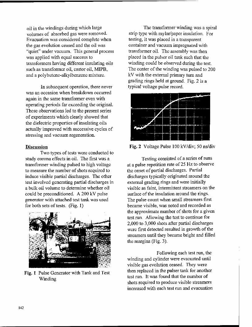
oil in the windings during which large volumes of absorbed gas were removed. Evacuation was considered complete when the gas evolution ceased and the oil was "quiet" under vacuum. This general process was applied with equal success to transformers having different insulating oils such as transformer oil, castor oil, MIPB, and a polybutene-alkylbenzene mixture.
In subsequent operation, there never was an occasion when breakdown occurred again in the same transformer even with operating periods far exceeding the original. These observations led to the present series of experiments which clearly showed that the dielectric properties of insulating oils actually improved with successive cycles of stressing and vacuum regeneration.
Discussion Two types of tests were conducted to
study corona effects in oil. The first was a transformer winding pulsed to high voltage to measure the number of shots required to induce visible partial discharges. The other test involved generating partial discharges in a bulk oil volume to determine whether oil could be preconditioned. A 200 kV pulse generator with attached test tank was used for both sets of tests. (Fig. 1)
The transformer winding was a spiral strip type with mylar/paper insulation. For testing, it was placed in a transparent container and vacuum impregnated with transformer oil. The assembly was then placed in the pulser oil tank such that the winding could be observed during the test. The center of the winding was pulsed to 200 kV with the external primary turn and grading rings held at ground. Fig. 2 is a typical voltage pulse record.
mnmm UMHUHB IHH9HHI MHMI
Fig. 1 Pulse Generator with Tank and Test Winding
Fig. 2 Voltage Pulse 100 kV/div; 50 ns/div
Testing consisted of a series of runs at a pulse repetition rate of 25 Hz to observe the onset of partial discharges. Partial discharges typically originated around the external grading rings and were initially visible as faint, intermittent streamers on the surface of the insulation around the rings. The pulse count when small streamers first became visible, was noted and recorded as the approximate number of shots for a given test run. Allowing the test to continue for 2,000 to 3,000 shots after partial discharges were first detected resulted in growth of the streamers until they became bright and filled the margins (Fig. 3).
Following each test run, the winding and cylinder were evacuated until visible gas evolution ceased. They were then replaced in the pulser tank for another test run. It was found that the number of shots required to produce visible streamers increased with each test run and evacuation
142
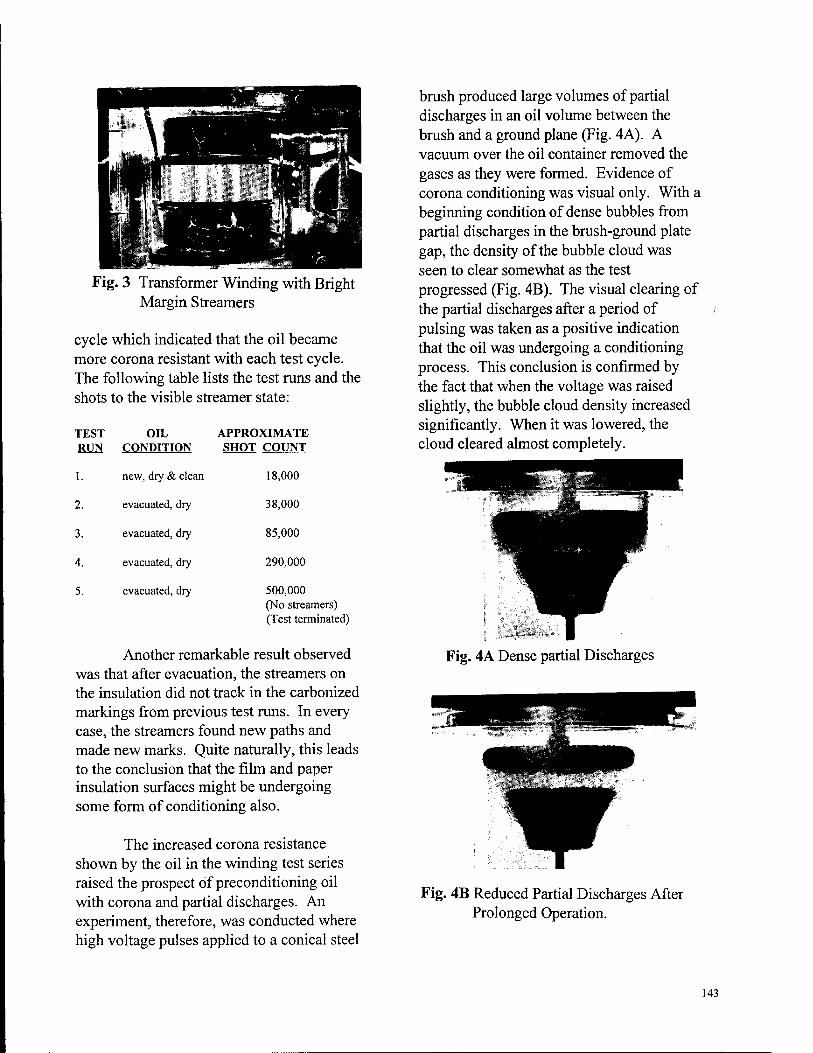
Fig. 3 Transformer Winding with Bright Margin Streamers
cycle which indicated that the oil became more corona resistant with each test cycle. The following table lists the test runs and the shots to the visible streamer state:
TEST OIL APPROXIMATE RUN CONDITION SHOT COUNT
1. new, dry & clean 18,000
2. evacuated, dry 38,000
3. evacuated, dry 85,000
4. evacuated, dry 290,000
5. evacuated, dry 500,000 (No streamers) (Test terminated)
Another remarkable result observed was that after evacuation, the streamers on the insulation did not track in the carbonized markings from previous test runs. In every case, the streamers found new paths and made new marks. Quite naturally, this leads to the conclusion that the film and paper insulation surfaces might be undergoing some form of conditioning also.
The increased corona resistance shown by the oil in the winding test series raised the prospect of preconditioning oil with corona and partial discharges. An experiment, therefore, was conducted where high voltage pulses applied to a conical steel
brush produced large volumes of partial discharges in an oil volume between the brush and a ground plane (Fig. 4A). A vacuum over the oil container removed the gases as they were formed. Evidence of corona conditioning was visual only. With a beginning condition of dense bubbles from partial discharges in the brush-ground plate gap, the density of the bubble cloud was seen to clear somewhat as the test progressed (Fig. 4B). The visual clearing of the partial discharges after a period of pulsing was taken as a positive indication that the oil was undergoing a conditioning process. This conclusion is confirmed by the fact that when the voltage was raised slightly, the bubble cloud density increased significantly. When it was lowered, the cloud cleared almost completely.
Fig. 4A Dense partial Discharges
Fig. 4B Reduced Partial Discharges After Prolonged Operation.
143
Conclusions It has been shown that the corona
resistance of insulating oils can be increased by repetitive cycles of operation or pre- stressing with evacuation. This process can not only extend the life of conventional components, but also permit designing systems and components for higher stress operation. For components such as transformers and capacitors that are assumed to be near the end of life when internal corona activity increases significantly, in- situ reprocessing may restore them to like- new condition. This process has been demonstrated with high voltage pulse transformers but remains to be shown for capacitors. Nevertheless, corona processing of insulating oils presents many prospects for innovative applications.
References 1. G.J. Rohwein, "Method and Apparatus for Regeneration of Oil", DOE Patent application SD-5392, SS-80, 840. 2. F.M. Clark, "Insulating Materials for Design and Engineering Practice ". John Wiley & Sons Inc., 1962. 3. W.T. Shugg, "Handbook of Electrical and Electronic Insulating Materials", Van Nostrard Reinhold Co., New York, 1986.
The prospect of pre-stressing insulating oils before installation in high voltage equipment opens the possibility of producing new generations of high energy density, long life components. Without pre- stressed oil such components would not be possible unless a new generation of oil were developed; a remote and expensive prospect at best.
144
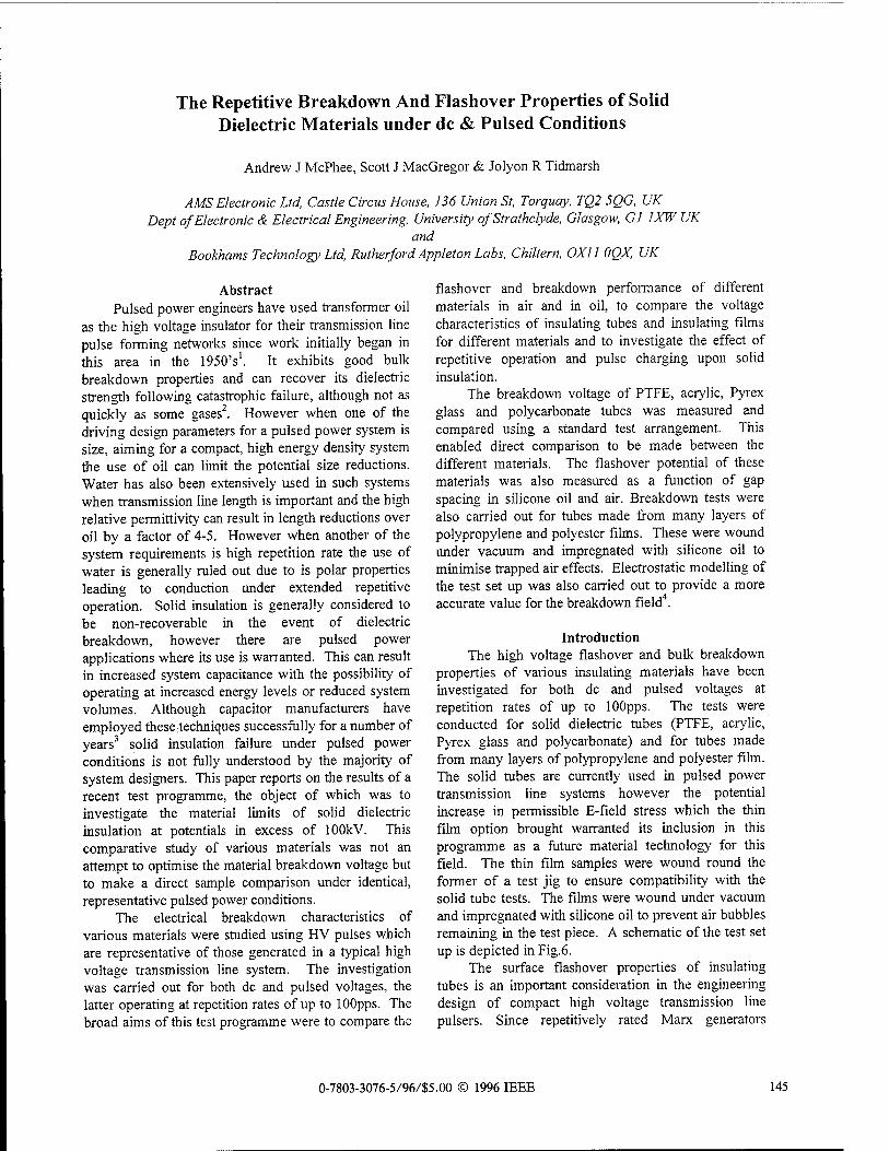
The Repetitive Breakdown And Flashover Properties of Solid Dielectric Materials under dc & Pulsed Conditions
Andrew J McPhee, Scott J MacGregor & Jolyon R Tidmarsh
AMS Electronic Ltd, Castle Circus House, 136 Union St, Torquay, TQ2 5QG, UK Dept of Electronic & Electrical Engineering, University of Strathclyde, Glasgow, Gl 1XW UK
and Bookhams Technology Ltd, Rutherford Appleton Labs, Chiltern, 0X11 OQX, UK
Abstract Pulsed power engineers have used transformer oil
as the high voltage insulator for their transmission line pulse forming networks since work initially began in this area in the 1950's1. It exhibits good bulk breakdown properties and can recover its dielectric strength following catastrophic failure, although not as quickly as some gases2. However when one of the driving design parameters for a pulsed power system is size, aiming for a compact, high energy density system the use of oil can limit the potential size reductions. Water has also been extensively used in such systems when transmission line length is important and the high relative permittivity can result in length reductions over oil by a factor of 4-5. However when another of the system requirements is high repetition rate the use of water is generally ruled out due to is polar properties leading to conduction under extended repetitive operation. Solid insulation is generally considered to be non-recoverable in the event of dielectric breakdown, however there are pulsed power applications where its use is warranted. This can result in increased system capacitance with the possibility of operating at increased energy levels or reduced system volumes. Although capacitor manufacturers have employed these techniques successfully for a number of years3 solid insulation failure under pulsed power conditions is not fully understood by the majority of system designers. This paper reports on the results of a recent test programme, the object of which was to investigate the material limits of solid dielectric insulation at potentials in excess of lOOkV. This comparative study of various materials was not an attempt to optimise the material breakdown voltage but to make a direct sample comparison under identical, representative pulsed power conditions.
The electrical breakdown characteristics of various materials were studied using HV pulses which are representative of those generated in a typical high voltage transmission line system. The investigation was carried out for both dc and pulsed voltages, the latter operating at repetition rates of up to lOOpps. The broad aims of this test programme were to compare the
flashover and breakdown performance of different materials in air and in oil, to compare the voltage characteristics of insulating tubes and insulating films for different materials and to investigate the effect of repetitive operation and pulse charging upon solid insulation.
The breakdown voltage of PTFE, acrylic, Pyrex glass and polycarbonate tubes was measured and compared using a standard test arrangement. This enabled direct comparison to be made between the different materials. The flashover potential of these materials was also measured as a function of gap spacing in silicone oil and air. Breakdown tests were also carried out for tubes made from many layers of polypropylene and polyester films. These were wound under vacuum and impregnated with silicone oil to minimise trapped air effects. Electrostatic modelling of the test set up was also carried out to provide a more accurate value for the breakdown field .
Introduction The high voltage flashover and bulk breakdown
properties of various insulating materials have been investigated for both dc and pulsed voltages at repetition rates of up to lOOpps. The tests were conducted for solid dielectric tubes (PTFE, acrylic, Pyrex glass and polycarbonate) and for tubes made from many layers of polypropylene and polyester film. The solid tubes are currently used in pulsed power transmission line systems however the potential increase in permissible E-field stress which the thin film option brought warranted its inclusion in this programme as a future material technology for this field. The thin film samples were wound round the former of a test jig to ensure compatibility with the solid tube tests. The films were wound under vacuum and impregnated with silicone oil to prevent air bubbles remaining in the test piece. A schematic of the test set up is depicted in Fig.6.
The surface flashover properties of insulating tubes is an important consideration in the engineering design of compact high voltage transmission line pulsers. Since repetitively rated Marx generators
0-7803-3076-5/96/S5.00 © 1996 IEEE 145
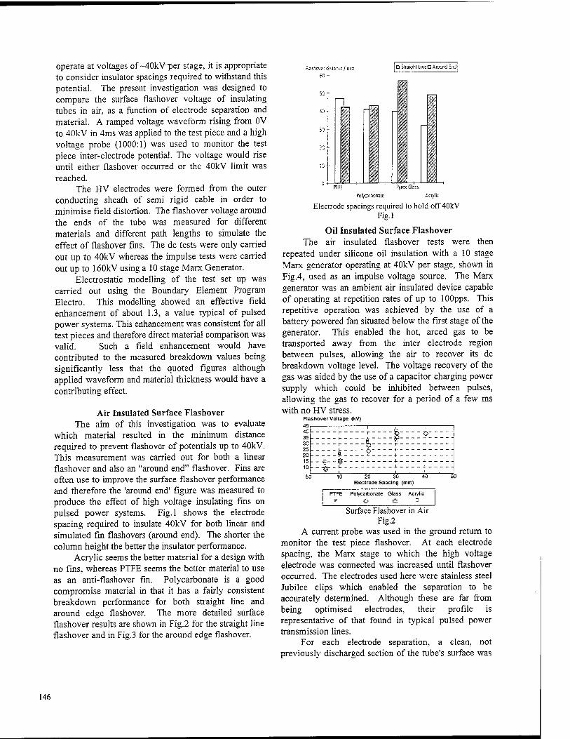
operate at voltages of ~40kV"per stage, it is appropriate to consider insulator spacings required to withstand this potential. The present investigation was designed to compare the surface flashover voltage of insulating tubes in air, as a function of electrode separation and material. A ramped voltage waveform rising from OV to 40kV in 4ms was applied to the test piece and a high voltage probe (1000:1) was used to monitor the test piece inter-electrode potential. The voltage would rise until either flashover occurred or the 40kV limit was reached.
The HV electrodes were formed from the outer conducting sheath of semi rigid cable in order to minimise field distortion. The flashover voltage around the ends of the tube was measured for different materials and different path lengths to simulate the effect of flashover fins. The dc tests were only carried out up to 40kV whereas the impulse tests were carried out up to 160kV using a 10 stage Marx Generator.
Electrostatic modelling of the test set up was carried out using the Boundary Element Program Electro. This modelling showed an effective field enhancement of about 1.3, a value typical of pulsed power systems. This enhancement was consistent for all test pieces and therefore direct material comparison was valid. Such a field enhancement would have contributed to the measured breakdown values being significantly less that the quoted figures although applied waveform and material thickness would have a contributing effect.
Air Insulated Surface Flashover The aim of this investigation was to evaluate
which material resulted in the minimum distance required to prevent flashover of potentials up to 40kV. This measurement was carried out for both a linear flashover and also an "around end" flashover. Fins are often use to improve the surface flashover performance and therefore the 'around end' figure was measured to produce the effect of high voltage insulating fins on pulsed power systems. Fig.l shows the electrode spacing required to insulate 40kV for both linear and simulated fin flashovers (around end). The shorter the column height the better the insulator performance.
Acrylic seems the better material for a design with no fins, whereas PTFE seems the better material to use as an anti-flashover fin. Polycarbonate is a good compromise material in that it has a fairly consistent breakdown performance for both straight line and around edge flashover. The more detailed surface flashover results are shown in Fig.2 for the straight line flashover and in Fig.3 for the around edge flashover.
Flasha-e: distance/mm
SO -T-
D Straight UrtenAround End
" PTFE Pyrex Glass
Polycarbonate Acrylic
Electrode spacings required to hold off 40kV Fig.l
Oil Insulated Surface Flashover The air insulated flashover tests were then
repeated under silicone oil insulation with a 10 stage Marx generator operating at 40kV per stage, shown in Fig.4, used as an impulse voltage source. The Marx generator was an ambient air insulated device capable of operating at repetition rates of up to 1 OOpps. This repetitive operation was achieved by the use of a battery powered fan situated below the first stage of the generator. This enabled the hot, arced gas to be transported away from the inter electrode region between pulses, allowing the air to recover its dc breakdown voltage level. The voltage recovery of the gas was aided by the use of a capacitor charging power supply which could be inhibited between pulses, allowing the gas to recover for a period of a few ms with no HV stress.
Flashover Voltage (kV) 45, , , , . , 40 . . B. j~
20 30 Electrode Spacing {mm)
Polycarbonate Glass
O O Acrylic
Surface Flashover in Air Fig.2
A current probe was used in the ground return to monitor the test piece flashover. At each electrode spacing, the Marx stage to which the high voltage electrode was connected was increased until flashover occurred. The electrodes used here were stainless steel Jubilee clips which enabled the separation to be accurately determined. Although these are far from being optimised electrodes, their profile is representative of that found in typical pulsed power transmission lines.
For each electrode separation, a clean, not previously discharged section of the tube's surface was
146
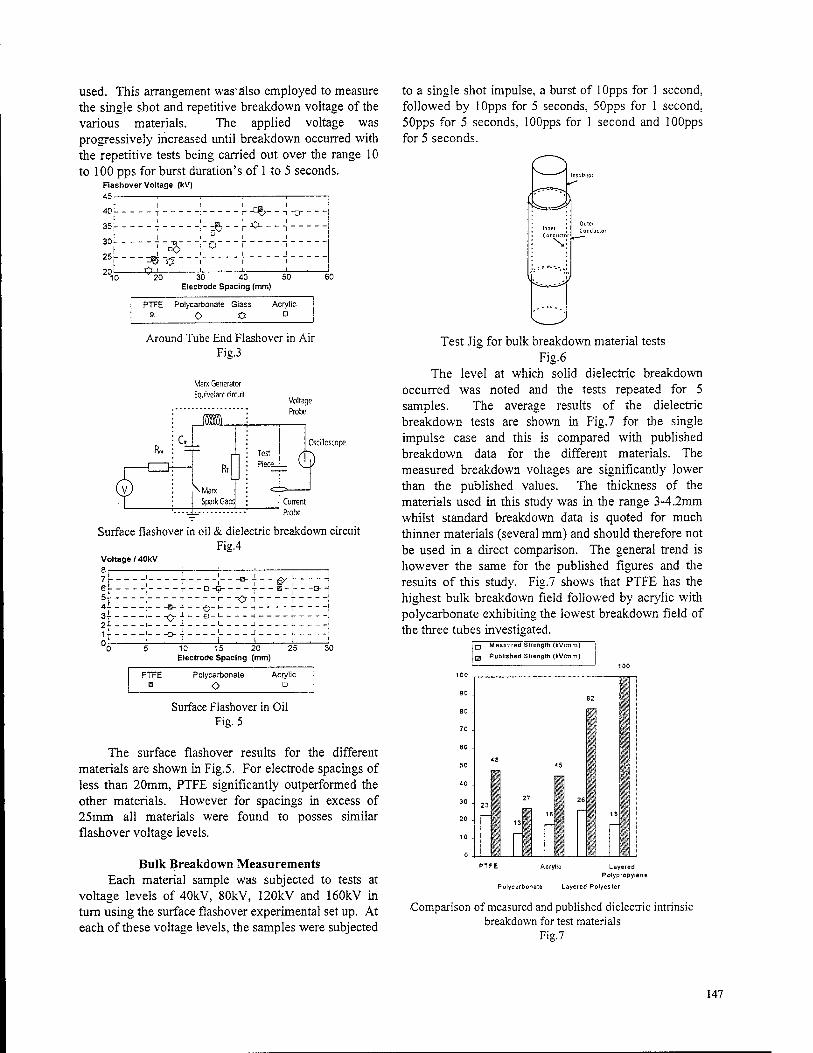
used. This arrangement was'also employed to measure the single shot and repetitive breakdown voltage of the various materials. The applied voltage was progressively increased until breakdown occurred with the repetitive tests being carried out over the range 10 to 100 pps for burst duration's of 1 to 5 seconds.
Flashover Voltage (kV) 45 , , , —
35 r 30 r
4 20^
"Ö"
O i 20 30 40
Electrode Spacing (mm)
Polycarbonate Glass
o o Acrylic.
D
Around Tube End Flashover in Air Fig.3
Surface flashover in oil & dielectric breakdown circuit Fig.4
Voltage / 40kV
5E: 3i- 2f - 1- - 0^
-D -tp- -
Xr{- -O
-o-i- -A — ^_ I .
10 15 20 Electrode Spacing (mm)
25 30
PTFE Polycarbonate
o Acrylic
D
Surface Flashover in Oil Fig. 5
The surface flashover results for the different materials are shown in Fig.5. For electrode spacings of less than 20mm, PTFE significantly outperformed the other materials. However for spacings in excess of 25mm all materials were found to posses similar flashover voltage levels.
Bulk Breakdown Measurements Each material sample was subjected to tests at
voltage levels of 40kV, 80kV, 120kV and 160kV in turn using the surface flashover experimental set up. At each of these voltage levels, the samples were subjected
to a single shot impulse, a burst of lOpps for 1 second, followed by lOpps for 5 seconds, 50pps for 1 second, 50pps for 5 seconds, lOOpps for 1 second and lOOpps for 5 seconds.
Test Jig for bulk breakdown material tests Fig.6
The level at which solid dielectric breakdown occurred was noted and the tests repeated for 5 samples. The average results of the dielectric breakdown tests are shown in Fig.7 for the single impulse case and this is compared with published breakdown data for the different materials. The measured breakdown voltages are significantly lower than the published values. The thickness of the materials used in this study was in the range 3-4.2mm whilst standard breakdown data is quoted for much thinner materials (several mm) and should therefore not be used in a direct comparison. The general trend is however the same for the published figures and the results of this study. Fig.7 shows that PTFE has the highest bulk breakdown field followed by acrylic with polycarbonate exhibiting the lowest breakdown field of the three tubes investigated.
□ Measured strength (kV/mm)
f3 Published Strength (kV/mm)
PTFE Acrylic
Polycarbonate Layered Polyester
Layered Polypropylene
■Comparison of measured and published dielectric intrinsic breakdown for test materials
Fig.7
147
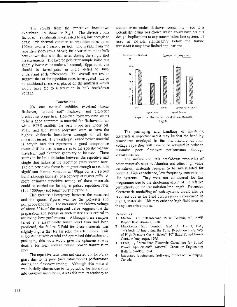
The results from the repetitive breakdown experiment are shown in Fig.8. The dielectric loss factor of the materials investigated being low enough to cause little thermal variation at repetition rates up to lOOpps over a 5 second period. The results from the repetitive study revealed very little variation in the bulk breakdown data with that taken during the single shot measurements. The layered polyester sample failed at a slightly lower value under a 1 second, lOpps burst, this should be investigated in more detail to fully understand such differences. The overall test results suggest that at the repetition rates investigated little or no additional stress was placed on the materials which would have led to a reduction in bulk breakdown voltage.
Conclusions No one material exhibits excellent linear
flashover, "around end" flashover and dielectric breakdown properties. However Polycarbonate seems to be a good compromise material for flashover in air while PTFE exhibits the best properties under oil. PTFE and the layered polyester seem to have the highest dielectric breakdown strength of all the materials tested. The workhorse pulsed power material is acrylic and this represents a good compromise material if the user is unsure as to the specific voltage waveform and electrode geometry to be used. There seems to be little deviation between the repetitive and single shot failure at the repetition rates studied here. The dielectric loss factor is not great enough to result in significant thermal variation at lOOpps for a 5 second burst although this may be a concern at higher prf s. A more stringent repetitive testing of these materials could be carried out for higher pulsed repetition rates (100-1000pps) and longer burst duration's.
The greatest discrepancy between the measured and the quoted figures was for the polyester and polypropylene film. The measured breakdown voltage of about 30% of the expected value suggests that the preparation and storage of such materials is critical to achieving best performance. Although these samples failed at a significantly lower level than had been predicted, the failure E-field for these materials was slightly higher that for the solid dielectric tubes. This suggests that with careful and optimised fabrication and packaging this route would give the optimum energy density for high voltage pulsed power transmission lines.
The repetitive tests were not carried out for Pyrex glass due to its poor (and catastrophic) performance during the flashover testing. Although this material was initially chosen due to its potential for fabrication into complex geometries, it was felt that its tendency to
shatter even under flashover conditions made it a potentially dangerous choice which could have serious design implications to any transmission line system. If used at E-fields significantly below the failure threshold it may have limited applications.
akdo'.vr, Field ikv/mm)
30 T
25 r i
20 I I
I 15
10 -
5
DSingleSliot QRepetitrve j
m p ii
PTFE Acrylic Layered Polypropylene
Polycarbonate Layered Polyester
Repetitive Dielectric Breakdown Results Fig.8
The packaging and handling of insulating materials is important and it may be that the handling procedures employed in the manufacture of high voltage capacitors will have to be adopted in order to minimise poor flashover performance through contamination.
The surface and bulk breakdown properties of other materials such as Alumina and other high value permittivity materials requires to be investigated for potential high capacitance, low frequency transmission line systems. They were not considered for this programme due to the shortening effect of the relative permittivity on the transmission line length. Extensive electrostatic modelling of such systems would also be required due to the field compression experienced in high 8r materials. This may enhance high field stress at the system triple points.
References 1 Martin, J.C., "Nanosecond Pulse Techniques", AWE
Report JCM/704-491, 1970. 2 MacGregor, S.J., Turnbull, S.M. & Tuema, F.A.,
"Methods of Improving the Pulse Repetition Frequency of High Pressure Gas Switches", 10th IEEE Pulsed Power Conf., Albuquerque, 1995.
3 Ennis, J., "Metallized Electrode Capacitors for Pulsed Power Applications", Maxwell Capacitor Engineering Bulletin 94-003, 1994.
4 Integrated Engineering Software, "Electro". Winnipeg, Canada.
148
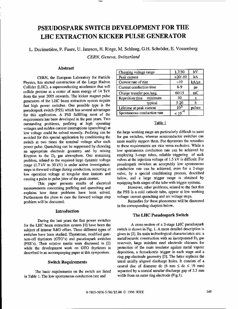
PSEUDOSPARK SWITCH DEVELOPMENT FOR THE LHC EXTRACTION KICKER PULSE GENERATOR
L. Ducimetiere, P. Faure, U. Jansson, H. Riege, M. Schlaug, G.H. Schröder, E. Vossenberg
CERN, Geneva, Switzerland
Abstract
CERN, the European Laboratory for Particle Physics, has started construction of the Large Hadron Collider (LHC), a superconducting accelerator that will collide protons at a center of mass energy of 14 TeV from the year 2005 onwards. The kicker magnet pulse generators of the LHC beam extraction system require fast high power switches. One possible type is the pseudospark switch (PSS) which has several advantages for this application. A PSS fulfilling most of the requirements has been developed in the past years. Two outstanding problems, prefiring at high operating voltages and sudden current interruptions (quenching) at low voltage could be solved recently. Prefiring can be avoided for this special application by conditioning the switch at two times the nominal voltage after each power pulse. Quenching can be suppressed by choosing an appropriate electrode geometry and by mixing Krypton to the D2 gas atmosphere. One remaining problem, related to the required large dynamic voltage range (1.7 kV to 30 kV) is under active investigation: steps in forward voltage during conduction, occurring at low operation voltage at irregular time instants and causing a pulse to pulse jitter of the peak current.
This paper presents results of electrical measurements concerning prefiring and quenching and explains how these problems have been solved. Furthermore the plans to cure the forward voltage step problem will be discussed.
Introduction
During the last years the fast power switches for the LHC beam extraction system [1] have been the subject of intense R&D effort. Three different types of switches have been studied. Thyratrons, modified gate- turn-off thyristors (GTO's) and pseudospark switches (PSS's). Their relative merits were discussed in [2] while the development work on GTO thyristors is described in an accompanying paper at this symposium.
Switch Requirements
The basic requirements on the switch are listed in Table 1. The low spontaneous conduction rate and
Charging voltage range 1.7/30 kV Peak current +20/-10 kA Current rate of rise -10 kA/us Current conduction time 8-9 us
Charge transfer pos./neg. 60/15 mC Repetition time minimum 30 s
typical 5-20 h Lifetime at peak current 103 pulses Spontaneous conduction rate <10"4
Table 1
the large working range are particularly difficult to meet for gas switches, whereas semiconductor switches can more readily support them. For thyratrons the remedies to these requirements are vice versa exclusive. While a low spontaneous conduction rate can be achieved by employing 3-stage tubes, reliable triggering of such valves at the injection voltage of 1.5 kV is difficult. For pseudospark switches an acceptably low spontaneous conduction rate can be achieved, even for a 2-stage valve, by a special conditioning process, described below, and a large trigger range is obtained by equipping both stages of the tube with trigger systems.
However, other problems, related to the fact that the PSS is a cold cathode tube, appear at low working voltage: current quenching and arc voltage steps.
Remedies for these phenomena will be discussed in the corresponding chapters below.
The LHC Pseudospark Switch
A cross-section of a 2-stage LHC pseudospark switch is shown in Fig. 1. A more detailed description is given in [2]. Its main technological characteristics are: a metal/ceramic construction with an incorporated D2 gas reservoir, large stainless steel electrode chicanes for protection of the main insulator against metal vapour deposition, a ferroelectric trigger in each stage and a ring gap electrode geometry [3]. The latter replaces the usual axially aligned discharge holes. It consists of a central disc of diameter dc (6 mm < dc < 19 mm) separated by a coaxial annular discharge gap of 2.5 mm width from an outer ring electrode (Fig.l).
0-7803-3076-5/96/S5.00 © 1996 IEEE 149
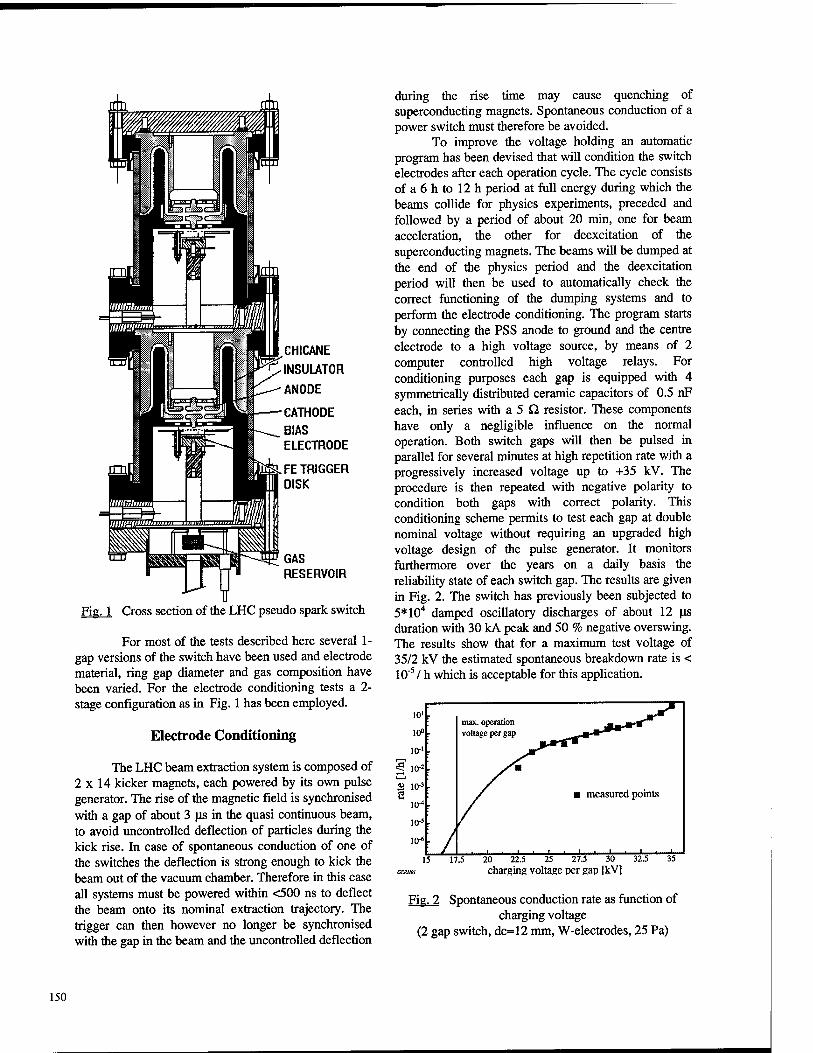
CHICANE
INSULATOR
ANODE
CATHODE
BIAS ELECTRODE
FE TRIGGER DISK
Up GAS RESERVOIR
Fig. 1 Cross section of the LHC pseudo spark switch
For most of the tests described here several 1- gap versions of the switch have been used and electrode material, ring gap diameter and gas composition have been varied. For the electrode conditioning tests a 2- stage configuration as in Fig. 1 has been employed.
Electrode Conditioning
The LHC beam extraction system is composed of 2 x 14 kicker magnets, each powered by its own pulse generator. The rise of the magnetic field is synchronised with a gap of about 3 us in the quasi continuous beam, to avoid uncontrolled deflection of particles during the kick rise. In case of spontaneous conduction of one of the switches the deflection is strong enough to kick the beam out of the vacuum chamber. Therefore in this case all systems must be powered within <500 ns to deflect the beam onto its nominal extraction trajectory. The trigger can then however no longer be synchronised with the gap in the beam and the uncontrolled deflection
during the rise time may cause quenching of superconducting magnets. Spontaneous conduction of a power switch must therefore be avoided.
To improve the voltage holding an automatic program has been devised that will condition the switch electrodes after each operation cycle. The cycle consists of a 6 h to 12 h period at full energy during which the beams collide for physics experiments, preceded and followed by a period of about 20 min, one for beam acceleration, the other for deexcitation of the superconducting magnets. The beams will be dumped at the end of the physics period and the deexcitation period will then be used to automatically check the correct functioning of the dumping systems and to perform the electrode conditioning. The program starts by connecting the PSS anode to ground and the centre electrode to a high voltage source, by means of 2 computer controlled high voltage relays. For conditioning purposes each gap is equipped with 4 symmetrically distributed ceramic capacitors of 0.5 riF each, in series with a 5 £2 resistor. These components have only a negligible influence on the normal operation. Both switch gaps will then be pulsed in parallel for several minutes at high repetition rate with a progressively increased voltage up to +35 kV. The procedure is then repeated with negative polarity to condition both gaps with correct polarity. This conditioning scheme permits to test each gap at double nominal voltage without requiring an upgraded high voltage design of the pulse generator. It monitors furthermore over the years on a daily basis the reliability state of each switch gap. The results are given in Fig. 2. The switch has previously been subjected to 5*104 damped oscillatory discharges of about 12 us duration with 30 kA peak and 50 % negative overswing. The results show that for a maximum test voltage of 35/2 kV the estimated spontaneous breakdown rate is < 10"5/ h which is acceptable for this application.
10'
10° max. operation
voltage per gap
10-'
1"10'2 2 10-' S
10"4
y/m
m measured points
io-5
10-6
17.5 20 22.5 25 27.5 30 32.5
charging voltage per gap [kVl 35
Fig. 2 Spontaneous conduction rate as function of charging voltage
(2 gap switch, dc=12 mm, W-electrodes, 25 Pa)
150
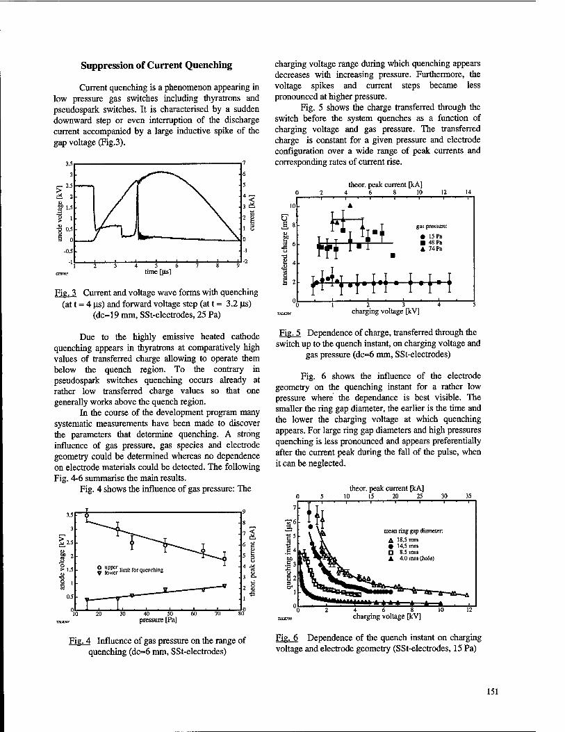
Suppression of Current Quenching
Current quenching is a phenomenon appearing in low pressure gas switches including thyratrons and pseudospark switches. It is characterised by a sudden downward step or even interruption of the discharge current accompanied by a large inductive spike of the gap voltage (Fig.3).
4 5 6 time [(is]
Fig.3 Current and voltage wave forms with quenching (at t = 4 us) and forward voltage step (at t = 3.2 us)
(dc=19 mm, SSt-electrodes, 25 Pa)
Due to the highly emissive heated cathode quenching appears in thyratrons at comparatively high values of transferred charge allowing to operate them below the quench region. To the contrary in pseudospark switches quenching occurs already at rather low transferred charge values so that one generally works above the quench region.
In the course of the development program many systematic measurements have been made to discover the parameters that determine quenching. A strong influence of gas pressure, gas species and electrode geometry could be determined whereas no dependence on electrode materials could be detected. The following Fig. 4-6 summarise the main results.
Fig. 4 shows the influence of gas pressure: The
40 50 pressure [Pa]
Fig. 4 Influence of gas pressure on the range of quenching (dc=6 mm, SSt-electrodes)
charging voltage range during which quenching appears decreases with increasing pressure. Furthermore, the voltage spikes and current steps became less pronounced at higher pressure.
Fig. 5 shows the charge transferred through the switch before the system quenches as a function of charging voltage and gas pressure. The transferred charge is constant for a given pressure and electrode configuration over a wide range of peak currents and corresponding rates of current rise.
theor. peak current [kA] 4 6 8 10 14
U £ 8
I 6
1 2
«71 gas pressure:
• 15 Pa ■ 48 Pa A 74 Pa
T H""
1 2 3 charging voltage [kV]
Fig. 5 Dependence of charge, transferred through the switch up to the quench instant, on charging voltage and
gas pressure (dc=6 mm, SSt-electrodes)
Fig. 6 shows the influence of the electrode geometry on the quenching instant for a rather low pressure where the dependance is best visible. The smaller the ring gap diameter, the earlier is the time and the lower the charging voltage at which quenching appears. For large ring gap diameters and high pressures quenching is less pronounced and appears preferentially after the current peak during the fall of the pulse, when it can be neglected.
theor. peak current [kA] 10 15 20 25 30 35
^6
•5 -
I4
■iri ' 1 ' 1
■ lit
"M***f
mean ring gap diameter A 18.5 mm • 14.5 mm D 8.5 mm A 4.0 mm (hole)
■+-*** * * * ■
charging voltage [kV] 10
Fig. 6 Dependence of the quench instant on charging voltage and electrode geometry (SSt-electrodes, 15 Pa)
151
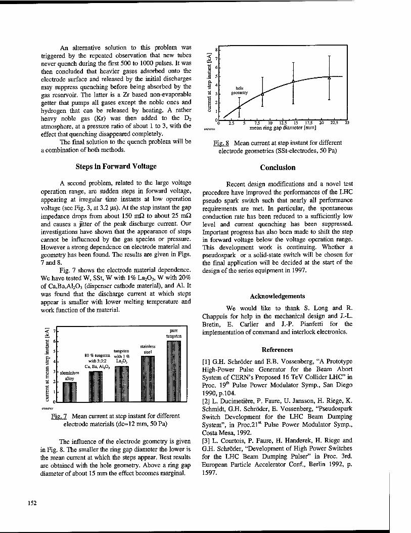
An alternative solution to this problem was triggered by the repeated observation that new tubes never quench during the first 500 to 1000 pulses. It was then concluded that heavier gases adsorbed onto the electrode surface and released by the initial discharges may suppress quenching before being absorbed by the gas reservoir. The latter is a Zr based non-evaporable getter that pumps all gases except the noble ones and hydrogen that can be released by heating. A rather heavy noble gas (Kr) was then added to the D2
atmosphere, at a pressure ratio of about 1 to 3, with the effect that quenching disappeared completely.
The final solution to the quench problem will be a combination of both methods.
Steps in Forward Voltage
2.5 5 7.5 10 12.5 15 17.5 20 mean ring gap diameter [mm]
Fig. 8 Mean current at step instant for different electrode geometries (SSt-electrodes, 50 Pa)
Conclusion
A second problem, related to the large voltage operation range, are sudden steps in forward voltage, appearing at irregular time instants at low operation voltage (see Fig. 3, at 3.2 us). At the step instant the gap impedance drops from about 150 mQ, to about 25 m£2 and causes a jitter of the peak discharge current. Our investigations have shown that the appearance of steps cannot be influenced by the gas species or pressure. However a strong dependence on electrode material and geometry has been found. The results are given in Figs. 7 and 8.
Fig. 7 shows the electrode material dependence. We have tested W, SSt, W with 1% La203, W with 20% of Ca,Ba,Al203 (dispenser cathode material), and Al. It was found that the discharge current at which steps appear is smaller with lower melting temperature and work function of the material.
I1
3 .9 5
P. B 4
r s g ' 3
tungsten 80 % tungsten wio, ] %
with 5:3:2 La203
Ca, Ba, A1203 n II ■ II pure
nrni
Fig. 7 Mean current at step instant for different electrode materials (dc=12 mm, 50 Pa)
The influence of the electrode geometry is given in Fig. 8. The smaller the ring gap diameter the lower is the mean current at which the steps appear. Best results are obtained with the hole geometry. Above a ring gap diameter of about 15 mm the effect becomes marginal.
Recent design modifications and a novel test procedure have improved the performances of the LHC pseudo spark switch such that nearly all performance requirements are met. In particular, the spontaneous conduction rate has been reduced to a sufficiently low level and current quenching has been suppressed. Important progress has also been made to shift the step in forward voltage below the voltage operation range. This development work is continuing. Whether a pseudospark or a solid-state switch will be chosen for the final application will be decided at the start of the design of the series equipment in 1997.
Acknowledgements
We would like to thank S. Long and R. Chappuis for help in the mechanical design and J.-L. Bretin, E. Carlier and J.-P. Pianfetti for the implementation of command and interlock electronics.
References
[1] G.H. Schröder and E.B. Vossenberg, "A Prototype High-Power Pulse Generator for the Beam Abort System of CERN's Proposed 16 TeV Collider LHC" in Proc. 19th Pulse Power Modulator Symp., San Diego 1990, p. 104. [2] L. Ducimetiere, P. Faure, U. Jansson, H. Riege, K. Schmidt, G.H. Schröder, E. Vossenberg, "Pseudospark Switch Development for the LHC Beam Dumping System", in Proc.21sl Pulse Power Modulator Symp., Costa Mesa, 1992. [3] L. Courtois, P. Faure, H. Handerek, H. Riege and G.H. Schröder, "Development of High Power Switches for the LHC Beam Dumping Pulser" in Proc. 3rd. European Particle Accelerator Conf., Berlin 1992, p. 1597.
152
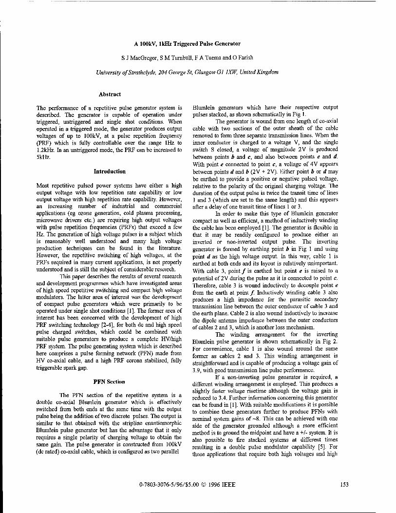
A lOOkV, 1kHz Triggered Pulse Generator
S J MacGregor, S M Turnbull, F A Tuema and O Farish
University of Strathclyde, 204 George St, Glasgow Gl 1XW, United Kingdom
Abstract
The performance of a repetitive pulse generator system is described. The generator is capable of operation under triggered, untriggered and single shot conditions. When operated in a triggered mode, the generator produces output voltages of up to lOOkV, at a pulse repetition frequency (PRF) which is fully controllable over the range 1Hz to 1.2kHz. In an untriggered mode, the PRF can be increased to 5kHz.
Introduction
Most repetitive pulsed power systems have either a high output voltage with low repetition rate capability or low output voltage with high repetition rate capability. However, an increasing number of industrial and commercial applications (eg ozone generation, cold plasma processing, microwave drivers etc.) are requiring high output voltages with pulse repetition frequencies (PRFs) that exceed a few Hz. The generation of high voltage pulses is a subject which is reasonably well understood and many high voltage production techniques can be found in the literature. However, the repetitive switching of high voltages, at the PRFs required in many current applications, is not properly understood and is still the subject of considerable research.
This paper describes the results of several research and development programmes which have investigated areas of high speed repetitive switching and compact high voltage modulators. The latter area of interest was the development of compact pulse generators which were primarily to be operated under single shot conditions [1]. The former area of interest has been concerned with the development of high PRF switching technology [2-4], for both dc and high speed pulse charged switches, which could be combined with suitable pulse generators to produce a complete HV/high PRF system. The pulse generating system which is described here comprises a pulse forming network (PFN) made from HV co-axial cable, and a high PRF corona stabilised, fully triggerable spark gap.
PFN Section
The PFN section of the repetitive system is a double co-axial Blumlein generator which is effectively switched from both ends at the same time with the output pulse being the addition of two discrete pulses. The output is similar to that obtained with the stripline enantiomorphic Blumlein pulse generator but has the advantage that it only requires a single polarity of charging voltage to obtain the same gain. The pulse generator is constructed from lOOkV (dc rated) co-axial cable, which is configured as two parallel
Blumlein generators which have their respective output pulses stacked, as shown schematically in Fig 1.
The generator is wound from one length of co-axial cable with two sections of the outer sheath of the cable removed to form three separate transmission lines. When the inner conductor is charged to a voltage V, and the single switch S closed, a voltage of magnitude 2V is produced between points b and c, and also between points e and d. With point e connected to point c, a voltage of 4V appears between points d and b (2V + 2V). Either point b or d may be earthed to provide a positive or negative pulsed voltage, relative to the polarity of the original charging voltage. The duration of the output pulse is twice the transit time of lines 1 and 3 (which are set to the same length) and this appears after a delay of one transit time of lines 1 or 3.
In order to make this type of Blumlein generator compact as well as efficient, a method of inductively winding the cable has been employed [1]. The generator is flexible in that it may be readily configured to produce either an inverted or non-inverted output pulse. The inverting generator is formed by earthing point A in Fig 1 and using point d as the high voltage output. In this way, cable 1 is earthed at both ends and its layout is relatively unimportant. With cable 3, point / is earthed but point e is raised to a potential of 2V during the pulse as it is connected to point c. Therefore, cable 3 is wound inductively to decouple point e from the earth at point/ Inductively winding cable 3 also produces a high impedance for the parasitic secondary transmission line between the outer conductor of cable 3 and the earth plane. Cable 2 is also wound inductively to increase the dipole antenna impedance between the outer conductors of cables 2 and 3, which is another loss mechanism.
The winding arrangement for the inverting Blumlein pulse generator is shown schematically in Fig 2. For convenience, cable 1 is also wound around the same former as cables 2 and 3. This winding arrangement is straightforward and is capable of producing a voltage gain of 3.9, with good transmission line pulse performance.
If a non-inverting pulse generator is required, a different winding arrangement is employed. This produces a slightly faster voltage risetime although the voltage gain is reduced to 3.4. Further information concerning this generator can be found in [1]. With suitable modifications it is possible to combine these generators further to produce PFNs with nominal system gains of ~8. This can be achieved with one side of the generator grounded although a more efficient method is to ground the midpoint and have a +/- system. It is also possible to fire stacked systems at different times resulting in a double pulse modulator capability [5]. For those applications that require both high voltages and high
0-7803-3076-5/96/S5.00 © 1996 IEEE 153
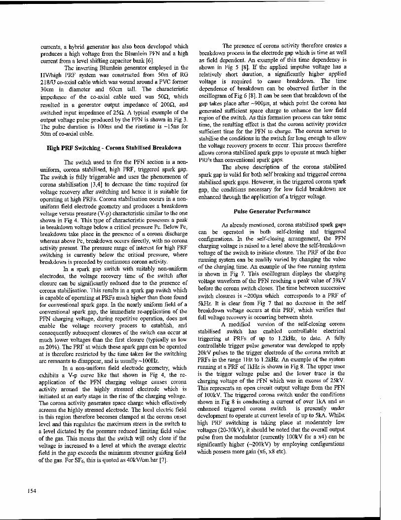
currents, a hybrid generator has also been developed which produces a high voltage from the Blumlein PFN and a high current from a level shifting capacitor bank [6].
The inverting Blumlein generator employed in the HV/high PRF system was constructed from 50m of RG 218/U co-axial cable which was wound around a PVC former 30cm in diameter and 60cm tall. The characteristic impedance of the co-axial cable used was 50Q, which resulted in a generator output impedance of 200Ü, and switched input impedance of 25Q. A typical example of the output voltage pulse produced by the PFN is shown in Fig 3. The pulse duration is 100ns and the risetime is ~15ns for 50m of co-axial cable.
High PRF Switching - Corona Stabilised Breakdown
The switch used to fire the PFN section is a non- uniform, corona stabilised, high PRF, triggered spark gap. The switch is fully triggerable and uses the phenomenon of corona stabilisation [3,4] to decrease the time required for voltage recovery after switching and hence it is suitable for operating at high PRFs. Corona stabilisation occurs in a non- uniform field electrode geometry and produces a breakdown voltage versus pressure (V-p) characteristic similar to the one shown in Fig 4. This type of characteristic possesses a peak in breakdown voltage below a critical pressure Pc. Below Pc, breakdown take place in the presence of a corona discharge whereas above Pc, breakdown occurs directly, with no corona activity present. The pressure range of interest for high PRF switching is currently below the critical pressure, where breakdown is preceded by continuous corona activity.
In a spark gap switch with suitably non-uniform electrodes, the voltage recovery time of the switch after closure can be significantly reduced due to the presence of corona stabilisation. This results in a spark gap switch which is capable of operating at PRFs much higher than those found for conventional spark gaps. In the nearly uniform field of a conventional spark gap, the immediate re-application of the PFN charging voltage, during repetitive operation, does not enable the voltage recovery process to establish, and consequently subsequent closures of the switch can occur at much lower voltages than the first closure (typically as low as 20%). The PRF at which these spark gaps can be operated at is therefore restricted by the time taken for the switching arc remnants to disappear, and is usually -100Hz.
In a non-uniform field electrode geometry, which exhibits a V-p curve like that shown in Fig 4, the re- application of the PFN charging voltage causes corona activity around the highly stressed electrode which is initiated at an early stage in the rise of the charging voltage. The corona activity generates space charge which effectively screens the highly stressed electrode. The local electric field in this region therefore becomes clamped at the corona onset level and this regulates the maximum stress in the switch to a level dictated by the pressure reduced limiting field value of the gas. This means that the switch will only close if the voltage is increased to a level at which the average electric field in the gap exceeds the minimum streamer guiding field of the gas. For SFö, this is quoted as 40kV/cm.bar [7].
The presence of corona activity therefore creates a breakdown process in the electrode gap which is time as well as field dependent. An example of this time dependency is shown in Fig 5 [8]. If the applied impulse voltage has a relatively short duration, a significantly higher applied voltage is required to cause breakdown. The time dependence of breakdown can be observed further in the oscillogram of Fig 6 [8]. It can be seen that breakdown of the gap takes place after ~900ns, at which point the corona has generated sufficient space charge to enhance the low field region of the switch. As this formation process can take some time, the resulting effect is that the corona activity provides sufficient time for the PFN to charge. The corona serves to stabilise the conditions in the switch for long enough to allow the voltage recovery process to occur. This process therefore allows corona stabilised spark gaps to operate at much higher PRFs than conventional spark gaps.
The above description of the corona stabilised spark gap is valid for both self breaking and triggered corona stabilised spark gaps. However, in the triggered corona spark gap, the conditions necessary for low field breakdown are enhanced through the application of a trigger voltage.
Pulse Generator Performance
As already mentioned, corona stabilised spark gaps can be operated in both self-closing and triggered configurations. In the self-closing arrangement, the PFN charging voltage is raised to a level above the self-breakdown voltage of the switch to initiate closure. The PRF of the free running system can be readily varied by changing the value of the charging time. An example of the free running system is shown in Fig 7. This oscillogram displays the charging voltage waveform of the PFN reaching a peak value of 39kV before the corona switch closes. The time between successive switch closures is ~200|as which corresponds to a PRF of 5kHz. It is clear from Fig 7 that no decrease in the self breakdown voltage occurs at this PRF, which verifies that full voltage recovery is occurring between shots.
A modified version of the self-closing corona stabilised switch has enabled controllable electrical triggering at PRFs of up to 1.2kHz, to date. A fully controllable trigger pulse generator was developed to apply 20kV pulses to the trigger electrode of the corona switch at PRFs in the range 1Hz to 1.2kHz. An example of the system running at a PRF of 1kHz is shown in Fig 8. The upper trace is the trigger voltage pulse and the lower trace is the charging voltage of the PFN which was in excess of 25kV. This represents an open circuit output voltage from the PFN of lOOkV. The triggered corona switch under the conditions shown in Fig 8 is conducting a current of over lkA and an enhanced triggered corona switch is presently under development to operate at current levels of up to 5kA. Whilst high PRF switching is taking place at moderately low voltages (20-30kV), it should be noted that the overall output pulse from the modulator (currently lOOkV for a x4) can be significantly higher (~200kV) by employing configurations which possess more gain (x6, x8 etc).
154
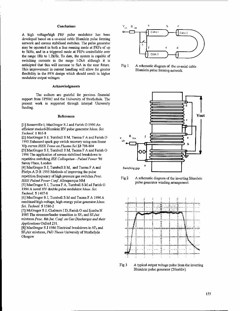
Conclusions
A high voltage/high PRF pulse modulator has been developed based on a co-axial cable Blumlein pulse forming network and corona stabilised switches. The pulse generator may be operated in both a free running mode at PRFs of up to 5kHz, and in a triggered mode at PRFs controllable over the range 1Hz to 1.2kHz. To date, the system is capable of switching currents in the range l-2kA although it is anticipted that this will increase to 5kA in the near future. This improvement in current handling will allow for greater flexibility in the PFN design which should result in higher modulator output voltages.
v,, R, b c
0—E3- ) Cable ' ) f) Cable 2
HEELD—([ Figl A schematic diagram of the co-axial cable
Blumlein pulse forming network.
Acknowledgments
The authors are grateful for previous financial support from EPSRC and the University of Strathclyde. The present work is supported through internal University funding.
References
[1] Somerville I, MacGregor S J and Farish O 1990 An efficient stacked-Blumlein HV pulse generator Meets. Sei. Technol. 1 865-8 [2] MacGregor S J, Tumbull S M, Tuema F A and Farish O 1995 Enhanced spark gap switch recovery using non-linear V/p curves IEEE Trans on Plasma Sei 23 798-804 [3] MacGregor S J, Turnbull S M, Tuema F A and Farish O 1996 The application of corona stabilised breakdown to repetitive switching IEE Colloquium - Pulsed Power '96 Savoy Place, London [4] MacGregor S J, Tumbull S M, and Tuema F A and Phelps ADR 1995 Methods of improving the pulse repetition frequency of high pressure gas switches Proc. IEEE Pulsed Power Conf. Albuquerque NM [5] MacGregor S J, Tuema F A, Turnbull S M ad Farish O 1994 A novel HV double pulse modulator Meas. Sei. Technol. 5 1407-8 [6] MacGregor S J, Tumbull S M and Tuema F A 1994 A combined high-voltage, high-energy pulse generator Meas. Sei. Technol. 5 1580-2 [7] McGregor S J, Chalmers ID, Farish O and Ijumba N 1985 The streamer/leader transition in SFö and SFe/air mixtures Proc. 8th Int. Conf. on Gas Discharges and their Applications Oxford 231. [8] MacGregor S J 1986 Electrical breakdown in SF« and SFö/air mixtures, PhD Thesis University of Strathclyde Glasgow
Vout
Switching gap
Fig 2 A schematic diagram of the inverting Blumlein pulse generator winding arrangement.
Fig 3 A typical output voltage pulse from the inverting Blumlein pulse generator (20ns/div).
155
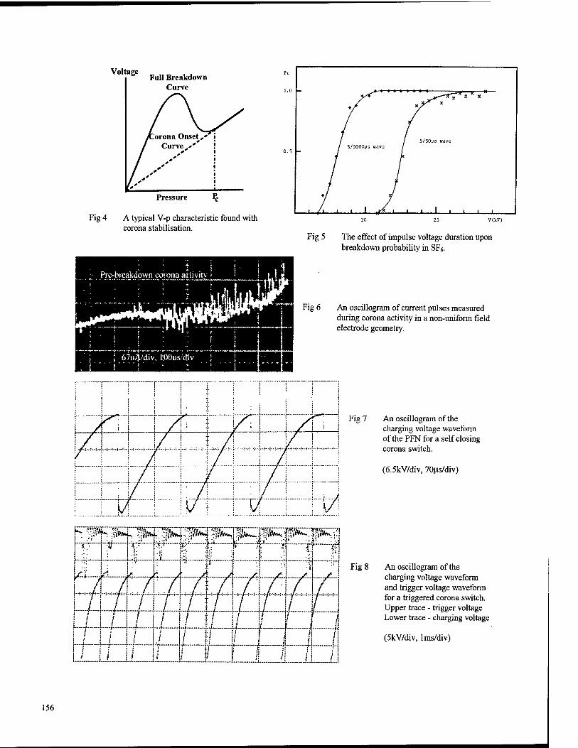
Voltage Full Breakdown
Curve
Pressure
Fig 4 A typical V-p characteristic found with corona stabilisation.
Fig 5 The effect of impulse voltage duration upon breakdown probability in SFö.
Fig 6 An oscillogram of current pulses measured during corona activity in a non-uniform field electrode geometry.
% ! 1 ■
i -i j
! T ;
■
J\ f ! """ ' ; i f \ -[-
.. / • f I \ \ y / \ T f
\ i / f / i
1- J A y
i j
\ \ !/ ; J V t \J\
j Fig 7 An oscillogram of the charging voltage waveform of the PFN for a self closing corona switch.
(6.5kV/div, 70ns/div)
/■-*■
*w
/
~pto<^ ^ifr^. •^V^-/ii!»*H: ^iW,
/
?<■**—. :ä.I...
...y
•A
;;jt*vw. iiii'if*^.
y- ./..
"ifVWi_ 'j
--/- Fig 8 An oscillogram of the
charging voltage waveform and trigger voltage waveform for a triggered corona switch. Upper trace - trigger voltage Lower trace - charging voltage
(5kV/div, lms/div)
156
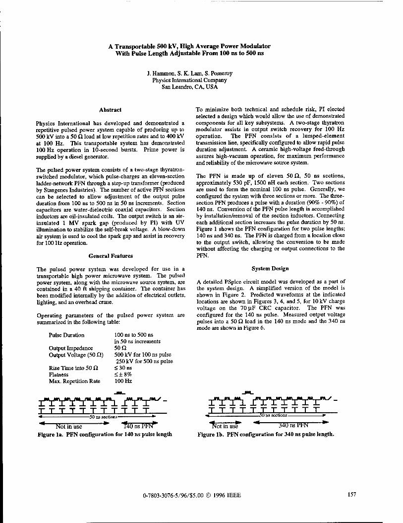
A Transportable 500 kV, High Average Power Modulator With Pulse Length Adjustable From 100 ns to 500 ns
J. Hanunon, S. K. Lam, S. Pomeroy Physics International Company
San Leandro, CA, USA
Abstract
Physics International has developed and demonstrated a repetitive pulsed power system capable of producing up to 500 kV into a 50 Q load at low repetition rates and to 400 kV at 100 Hz. This transportable system has demonstrated 100 Hz operation in 10-second bursts. Prime power is supplied by a diesel generator.
The pulsed power system consists of a two-stage thyratron- switched modulator, which pulse-charges an eleven-section ladder-network PFN through a step-up transformer (produced by Stangenes Industries). The number of active PFN sections can be selected to allow adjustment of the output pulse duration from 100 ns to 500 ns in 50 ns increments. Section capacitors are water-dielectric coaxial capacitors. Section inductors are oil-insulated coils. The output switch is an air- insulated 1 MV spark gap (produced by PI) with UV illumination to stabilize the self-break voltage. A blow-down air system is used to cool the spark gap and assist in recovery for 100 Hz operation.
General Features
The pulsed power system was developed for use in a transportable high power microwave system. The pulsed power system, along with the microwave source system, are contained in a 40 ft shipping container. The container has been modified internally by the addition of electrical outlets, lighting, and an overhead crane.
Operating parameters of the pulsed power system are summarized in the following table:
Pulse Duration
Output Impedance Output Voltage (50 Q)
Rise Time into 50 Q Flatness Max. Repetition Rate
100 ns to 500 ns in 50 ns increments 50 Q 500 kV for 100 ns pulse 250 kV for 500 ns pulse £30ns !£±8% 100 Hz
ifT^fYY^L JTITJ^ TTTTTTTTTTT ^ 50 ns sections
"* Not in use *" "T40 ns PFN*~ Figure la. PFN configuration for 140 ns pulse length
To minimize both technical and schedule risk, PI elected selected a design which would allow the use of demonstrated components for all key subsystems. A two-stage thyratron modulator assists in output switch recovery for 100 Hz operation. The PFN consists of a lumped-element transmission line, specifically configured to allow rapid pulse duration adjustment. A ceramic high-voltage feed-through assures high-vacuum operation, for maximum performance and reliability of the microwave source system.
The PFN is made up of eleven 50 £1, 50 ns sections, approximately 530 pF, 1500 nH each section. Two sections are used to form the nominal 100 ns pulse. Generally, we configured the system with three sections or more. The three- section PFN produces a pulse with a duration (90% - 90%) of 140 ns. Conversion of the PFN pulse length is accomplished by installation/removal of the section inductors. Connecting each additional section increases the pulse duration by 50 ns. Figure 1 shows the PFN configuration for two pulse lengths; 140 ns and 340 ns. The PFN is charged from a location close to the output switch, allowing the conversion to be made without affecting the charging or output connections to the PFN.
System Design
A detailed PSpice circuit model was developed as a part of the system design. A simplified version of the model is shown in Figure 2. Predicted waveforms at the indicated locations are shown in Figures 3, 4, and 5, for 10 kV charge voltage on the 70 uF CRC capacitor. The PFN was configured for the 140 ns pulse. Measured output voltage pulses into a 50 Q load in the 140 ns mode and the 340 ns mode are shown in Figure 6.
_m_
TTTTTTTTTTT 50 ns sections -
"^JÖ <otinu"se ^ 340 ns PFN " Figure lb. PFN configuration for 340 ns pulse length.
0-7803-3076-5/96/S5.00 © 1996 IEEE 157
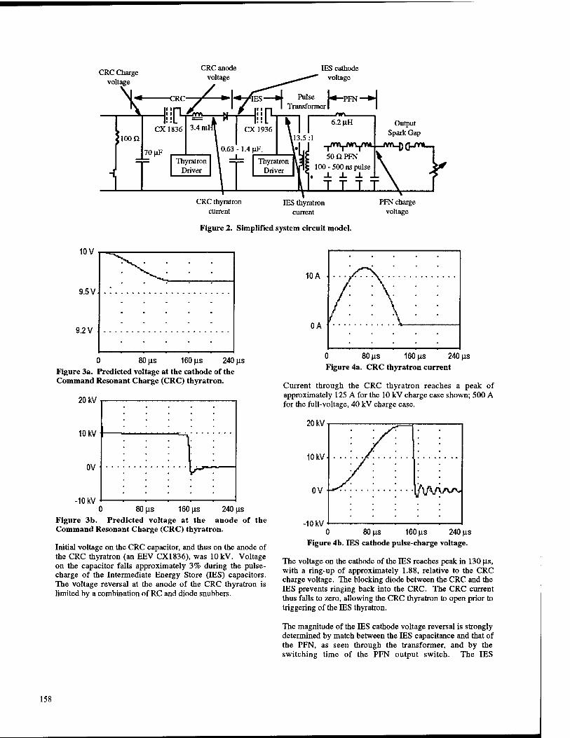
CRC Charge voltage
CRC anode voltage
Pulse Transformer
IES cathode voltage
p—PFN—»■
6.2 uH
50 Q PFN 100 - 500 ns pulse
_L J_ J. _L T T T
Output Spark Gap
CRC thyratron current
IES thyratron current
PFN charge voltage
Figure 2. Simplified system circuit model.
10 V
9.5 V
9.2 V
0 80 ns 160 us 240 ns Figure 3a. Predicted voltage at the cathode of the Command Resonant Charge (CRC) thyratron.
20 kV
10 kV
-10 kV 0 80 (is 160 (is 240 (is
Figure 3b. Predicted voltage at the anode of the Command Resonant Charge (CRC) thyratron.
Initial voltage on the CRC capacitor, and thus on the anode of the CRC thyratron (an EEV CX1836), was 10 kV. Voltage on the capacitor falls approximately 3% during the pulse- charge of the Intermediate Energy Store (IES) capacitors. The voltage reversal at the anode of the CRC thyratron is limited by a combination of RC and diode snubbers.
10 A
0A
0 80 us 160 us 240 us Figure 4a. CRC thyratron current
Current through the CRC thyratron reaches a peak of approximately 125 A for the 10 kV charge case shown; 500 A for the full-voltage, 40 kV charge case.
20 kV
10 kV
: :
/l/\A/w ov
-10kV 0 80 us 160 us 240 us
Figure 4b. IES cathode pulse-charge voltage.
The voltage on the cathode of the IES reaches peak in 130 us, with a ring-up of approximately 1.88, relative to the CRC charge voltage. The blocking diode between the CRC and the IES prevents ringing back into the CRC. The CRC current thus falls to zero, allowing the CRC thyratron to open prior to triggering of the IES thyratron.
The magnitude of the IES cathode voltage reversal is strongly determined by match between the IES capacitance and that of the PFN, as seen through the transformer, and by the switching time of the PFN output switch. The IES
158
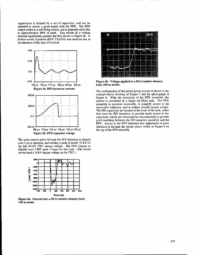
capacitance is formed by a set of capacitors, and can be adjusted to assure a good match with the PFN. The PFN output switch is a self-firing switch, and is generally set to fire at approximately 90% of peak. This results in a voltage reversal significantly greater that that shown in Figure 4b. A hollow-anode thyratron (EEV CX1936) was selected due to its tolerance of this type of reversal.
4kA
2kA
OA
-2kA 150us 160us 170us 180us 190us 200us
Figure 5a. IES thyratron current
400 kV
200 kV
-200 kV 150 us 152 ns 154 us 156 ns 158 us 160 us
Figure 5b. PFN capacitor voltage.
The main current pulse through the IES thyratron is slightly over 5 |is in duration, and reaches a peak of nearly 12 kA for the full 40 kV CRC charge voltage. The PFN charges to slightly over 1 MV peak voltage for this case. (The model shown used a 10 kV charge voltage on the CRC.)
Figure 6b. Voltage applied to a 50 Q. resistive dummy load; 350 ns modes.
The configuration of the pulsed power system is shown in the concept layout drawing of Figure 7 and the photograph of Figure 8. With the exception of the PFN assembly, the system is contained in a single oil-filled tank. The PFN assembly is mounted externally, to simplify access to the removable inductors, and to reduce overall system weight. The IES capacitors are located at the front of the tank, rather than near the IES thyratron, to provide ready access to the capacitors, which are connected (or disconnected) to provide good matching between the IES capacitor assembly and the PFN. Access to the PFN inductors (for adjustment of pulse duration) is through the square plates visible in Figure 8 on the top of the PFN assembly.
£000
lh i
r r^
"8 jj -woo
W r •14000
-<00 -200 100 «00 1000 200 400
Time (ns)
Figure 6a. Current into a 50 Q resistive dummy load; 140 ns mode.
159
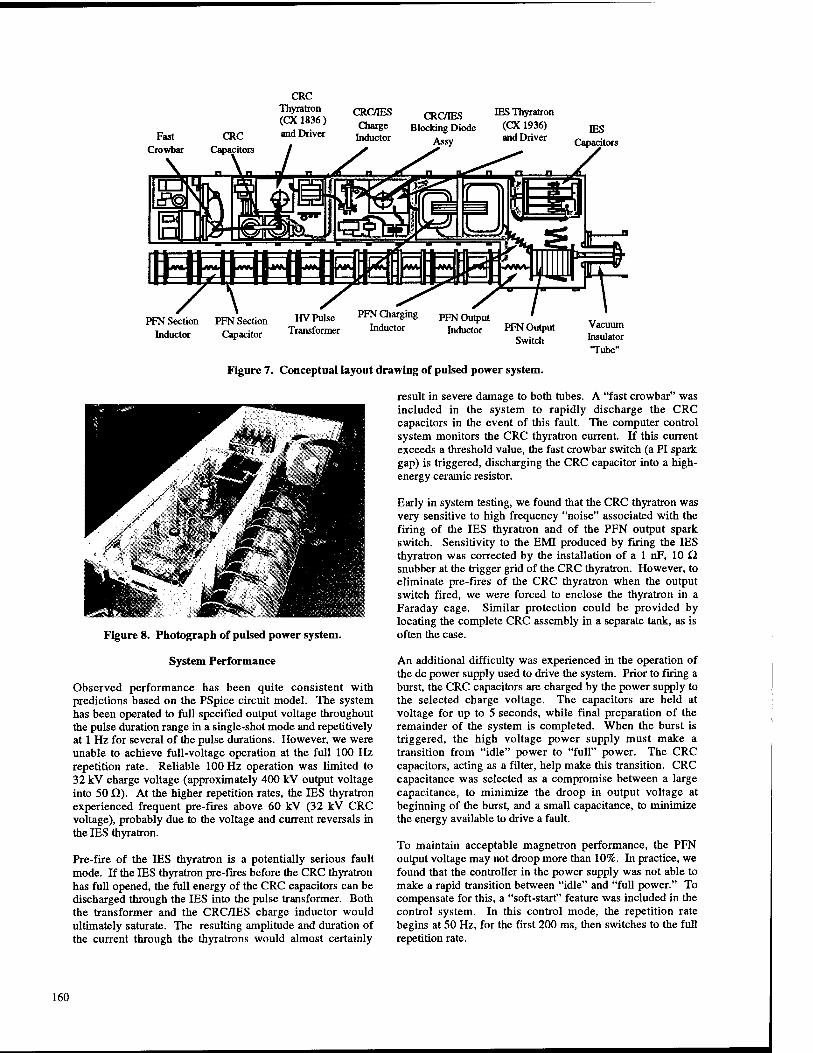
Fast Crowbar
CRC Capacitors
CRC Thyratron (CX1836) and Driver
CRC/EES CRC/mS Charge Blocking Diode
Inductor Assy
IES Thyratron (CX 1936) and Driver
IES Capacitors
PFN Section Inductor
PFN Section Capacitor
HV Pulse Transformer
PFN Charging Inductor
PFN Output Inductor PFN Output
Switch
Vacuum Insulator 'Tube"
Figure 7. Conceptual layout drawing of pulsed power system.
Figure 8. Photograph of pulsed power system.
System Performance
Observed performance has been quite consistent with predictions based on the PSpice circuit model. The system has been operated to full specified output voltage throughout the pulse duration range in a single-shot mode and repetitively at 1 Hz for several of the pulse durations. However, we were unable to achieve full-voltage operation at the full 100 Hz repetition rate. Reliable 100 Hz operation was limited to 32 kV charge voltage (approximately 400 kV output voltage into 50 Q). At the higher repetition rates, the IES thyratron experienced frequent pre-fires above 60 kV (32 kV CRC voltage), probably due to the voltage and current reversals in the IES thyratron.
Pre-fire of the IES thyratron is a potentially serious fault mode. If the IES thyratron pre-fires before the CRC thyratron has full opened, the full energy of the CRC capacitors can be discharged through the IES into the pulse transformer. Both the transformer and the CRC/IES charge inductor would ultimately saturate. The resulting amplitude and duration of the current through the thyratrons would almost certainly
result in severe damage to both tubes. A "fast crowbar" was included in the system to rapidly discharge the CRC capacitors in the event of this fault. The computer control system monitors the CRC thyratron current. If this current exceeds a threshold value, the fast crowbar switch (a PI spark gap) is triggered, discharging the CRC capacitor into a high- energy ceramic resistor.
Early in system testing, we found that the CRC thyratron was very sensitive to high frequency "noise" associated with the firing of the IES thyratron and of the PFN output spark switch. Sensitivity to the EMI produced by firing the IES thyratron was corrected by the installation of a 1 nF, 10 £1 snubber at the trigger grid of the CRC thyratron. However, to eliminate pre-fires of the CRC thyratron when the output switch fired, we were forced to enclose the thyratron in a Faraday cage. Similar protection could be provided by locating the complete CRC assembly in a separate tank, as is often the case.
An additional difficulty was experienced in the operation of the dc power supply used to drive the system. Prior to firing a burst, the CRC capacitors are charged by the power supply to the selected charge voltage. The capacitors are held at voltage for up to 5 seconds, while final preparation of the remainder of the system is completed. When the burst is triggered, the high voltage power supply must make a transition from "idle" power to "full" power. The CRC capacitors, acting as a filter, help make this transition. CRC capacitance was selected as a compromise between a large capacitance, to minimize the droop in output voltage at beginning of the burst, and a small capacitance, to minimize the energy available to drive a fault.
To maintain acceptable magnetron performance, the PFN output voltage may not droop more than 10%. In practice, we found that the controller in the power supply was not able to make a rapid transition between "idle" and "full power." To compensate for this, a "soft-start" feature was included in the control system. In this control mode, the repetition rate begins at 50 Hz, for the first 200 ms, then switches to the full repetition rate.
160
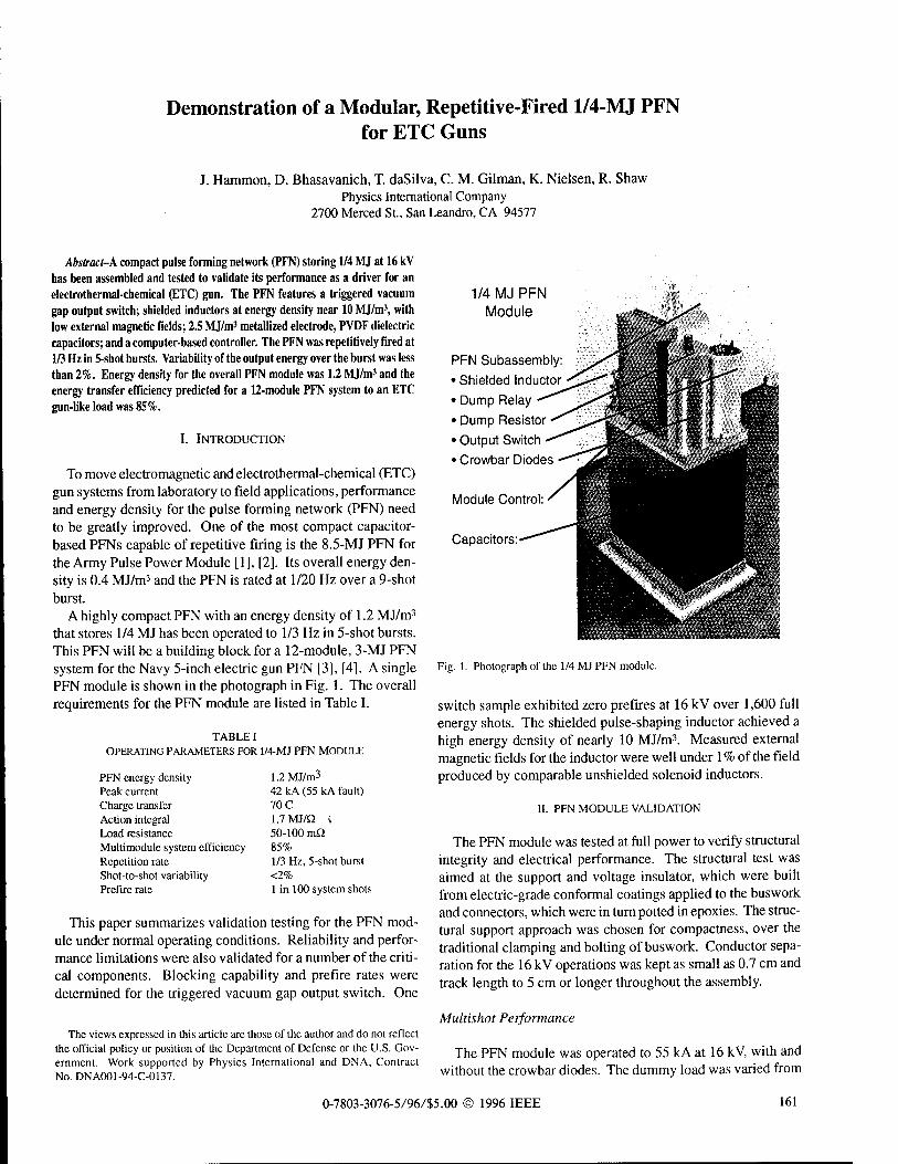
Demonstration of a Modular, Repetitive-Fired 1/4-MJ PFN for ETC Guns
J. Hammon, D. Bhasavanich, T. daSilva, C. M. Gilman, K. Nielsen, R. Shaw Physics International Company
2700 Merced St., San Leandro, CA 94577
Abstract-k compact pulse forming network (PFN) storing 1/4 MJ at 16 kV has been assembled and tested to validate its performance as a driver for an electrothermal-chemical (ETC) gun. The PFN features a triggered vacuum gap output switch; shielded inductors at energy density near 10 MJ/m3, with low external magnetic fields; 2.5 MJ/m3 metallized electrode, PVDF dielectric capacitors; and a computer-based controller. The PFN was repetitively fired at 1/3 Hz in 5-shot bursts. Variability of the output energy over the burst was less than 2%. Energy density for the overall PFN module was 1.2 MJ/m3 and the energy transfer efficiency predicted for a 12-module PFN system to an ETC gun-like load was 85%.
I. INTRODUCTION
To move electromagnetic and electrothermal-chemical (ETC) gun systems from laboratory to field applications, performance and energy density for the pulse forming network (PFN) need to be greatly improved. One of the most compact capacitor- based PFNs capable of repetitive firing is the 8.5-MJ PFN for the Army Pulse Power Module [1 ], [2]. Its overall energy den- sity is 0.4 MJ/m3 and the PFN is rated at 1/20 Hz over a 9-shot burst.
A highly compact PFN with an energy density of 1.2 MJ/m3
that stores 1/4 MJ has been operated to 1/3 Hz in 5-shot bursts. This PFN will be a building block for a 12-module, 3-MJ PFN system for the Navy 5-inch electric gun PFN [3], [4]. A single PFN module is shown in the photograph in Fig. 1. The overall requirements for the PFN module are listed in Table I.
TABLE I OPERATING PARAMETERS FOR 1/4-MJ PFN MODULE
PFN energy density Peak current Charge transfer Action integral Load resistance Multimodule system efficiency Repetition rale Shot-to-shot variability Prcfirc rale
1.2MJ/m3 42 kA (55 kA fault) 70 C 1.7MM2 < 50-100 mQ 85% 1/3 Hz, 5-shot burst <2% 1 in 100 system shots
This paper summarizes validation testing for the PFN mod- ule under normal operating conditions. Reliability and perfor- mance limitations were also validated for a number of the criti- cal components. Blocking capability and prefire rates were determined for the triggered vacuum gap output switch. One
The views expressed in this article arc those of the author and do not reflect the official policy or position of the Department of Defense or the U.S. Gov- ernment. Work supported by Physics International and DNA, Contract No. DNA001-94-C-0137.
1/4 MJ PFN Module
PFN Subassembly:
• Shielded Inductor
• Dump Relay
• Dump Resistor
• Output Switch
• Crowbar Diodes
Module Control
Capacitors:
Fig. 1. Photograph of the 1/4 MJ PFN module.
switch sample exhibited zero prefires at 16 kV over 1,600 full energy shots. The shielded pulse-shaping inductor achieved a high energy density of nearly 10 MJ/m3. Measured external magnetic fields for the inductor were well under 1% of the field produced by comparable unshielded solenoid inductors.
II. PFN MODULE VALIDATION
The PFN module was tested at full power to verify structural integrity and electrical performance. The structural test was aimed at the support and voltage insulator, which were built from electric-grade conformal coatings applied to the buswork and connectors, which were in turn potted in epoxies. The struc- tural support approach was chosen for compactness, over the traditional clamping and bolting of buswork. Conductor sepa- ration for the 16 kV operations was kept as small as 0.7 cm and track length to 5 cm or longer throughout the assembly.
Multishot Performance
The PFN module was operated to 55 kA at 16 kV, with and without the crowbar diodes. The dummy load was varied from
0-7803-3076-5/96/S5.00 © 1996 IEEE 161
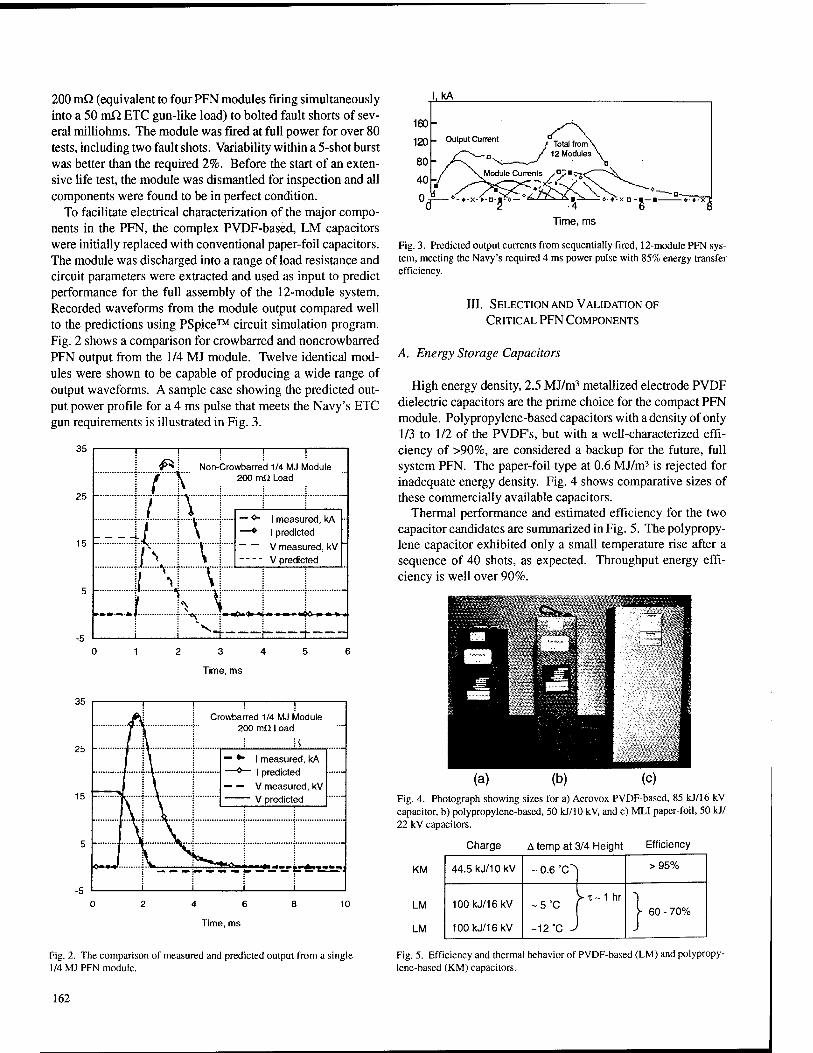
200 mQ (equivalent to four PFN modules firing simultaneously into a 50 m£2 ETC gun-like load) to bolted fault shorts of sev- eral milliohms. The module was fired at full power for over 80 tests, including two fault shots. Variability within a 5-shot burst was better than the required 2%. Before the start of an exten- sive life test, the module was dismantled for inspection and all components were found to be in perfect condition.
To facilitate electrical characterization of the major compo- nents in the PFN, the complex PVDF-based, LM capacitors were initially replaced with conventional paper-foil capacitors. The module was discharged into a range of load resistance and circuit parameters were extracted and used as input to predict performance for the full assembly of the 12-module system. Recorded waveforms from the module output compared well to the predictions using PSpice™ circuit simulation program. Fig. 2 shows a comparison for crowbarred and noncrowbarred PFN output from the 1/4 MJ module. Twelve identical mod- ules were shown to be capable of producing a wide range of output waveforms. A sample case showing the predicted out- put power profile for a 4 ms pulse that meets the Navy's ETC gun requirements is illustrated in Fig. 3.
I, kA
35
25
15
rffi Non-Crowbarred 1/4 MJ Module
200 mO Load
:::ii::n
J
■ *■ I measured, kA -* I predicted
— V measured, kV — V predicted
_l_ it: -Jzi
Time, ms
"! ! ! ! Crowbarred 1/4 MJ Module
200 m!! Load
— *" I measured, kA I predicted
— — V measured, kV V predicted
Time, ms
Fig. 3. Predicted output currents from sequentially fired, 12-modulc PFN sys- tem, meeting the Navy's required 4 ms power pulse with 85% energy transfer efficiency.
HI. SELECTION AND VALIDATION OF
CRITICAL PFN COMPONENTS
A. Energy Storage Capacitors
High energy density, 2.5 MJ/m3 metallized electrode PVDF dielectric capacitors are the prime choice for the compact PFN module. Polypropylene-based capacitors with a density of only 1/3 to 1/2 of the PVDF's, but with a well-characterized effi- ciency of >90%, are considered a backup for the future, full system PFN. The paper-foil type at 0.6 MJ/m3 is rejected for inadequate energy density. Fig. 4 shows comparative sizes of these commercially available capacitors.
Thermal performance and estimated efficiency for the two capacitor candidates are summarized in Fig. 5. The polypropy- lene capacitor exhibited only a small temperature rise after a sequence of 40 shots, as expected. Throughput energy effi- ciency is well over 90%.
Fig. 4. Photograph showing sizes for a) Acrovox PVDF-based, 85 kJ/16 kV capacitor, b) polypropylene-based, 50 kJ/10 kV, and c) MLI paper-foil, 50 kJ/ 22 kV capacitors.
KM
Charge A temp at 3/4 Height Efficiency
44.5kJ/10kV - 0.6 'C > 95%
100kJ/16kV
100kJ/16kV
~5°C
-12 °C -
> T - 1 hr > 60-70%
Fig. 2. The comparison of measured and predicted output from a single 1/4 MJ PFN module.
LM
LM
Fig. 5. Efficiency and thermal behavior of PVDF-based (LM) and polypropy- lcnc-bascd (KM) capacitors.
162
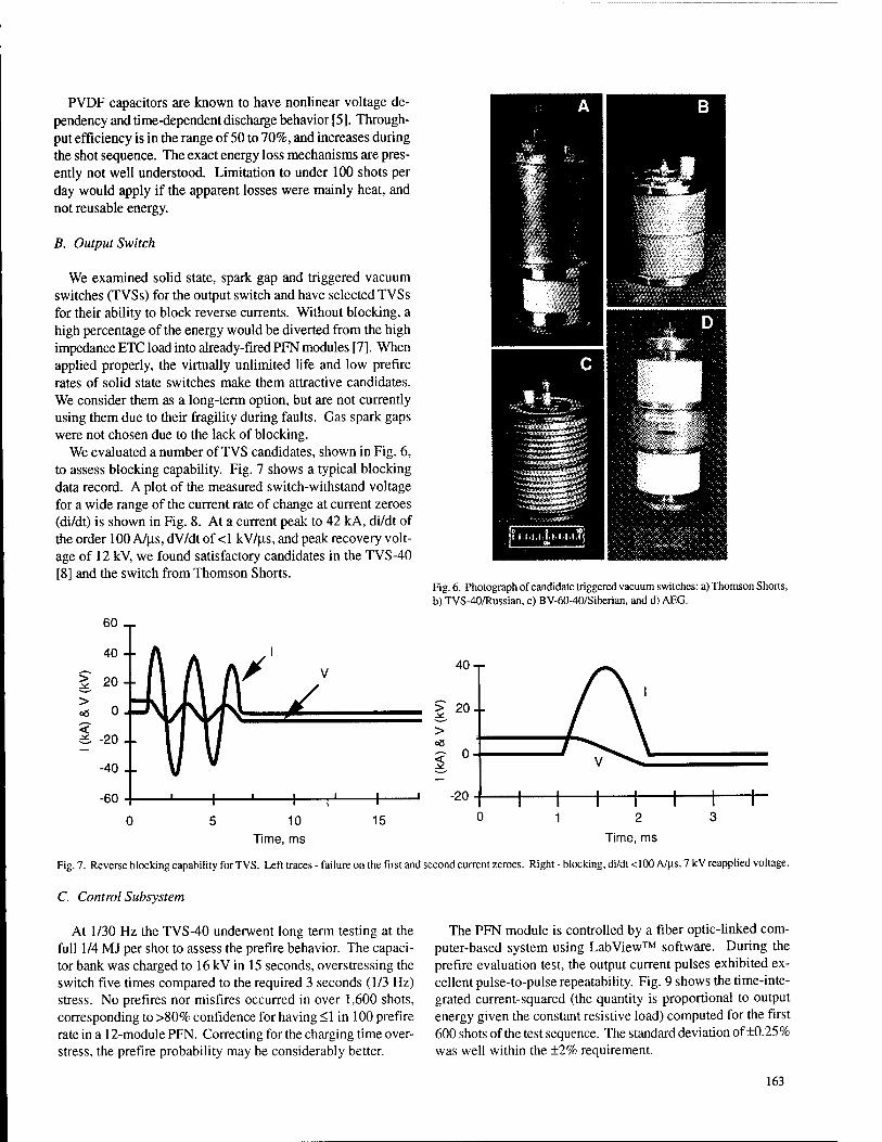
PVDF capacitors are known to have nonlinear voltage de- pendency and time-dependent discharge behavior [5]. Through- put efficiency is in the range of 50 to 70%, and increases during the shot sequence. The exact energy loss mechanisms are pres- ently not well understood. Limitation to under 100 shots per day would apply if the apparent losses were mainly heat, and not reusable energy.
B. Output Switch
We examined solid state, spark gap and triggered vacuum switches (TVSs) for the output switch and have selected TVSs for their ability to block reverse currents. Without blocking, a high percentage of the energy would be diverted from the high impedance ETC load into already-fired PFN modules [7]. When applied properly, the virtually unlimited life and low prefire rates of solid state switches make them attractive candidates. We consider them as a long-term option, but are not currently using them due to their fragility during faults. Gas spark gaps were not chosen due to the lack of blocking.
We evaluated a number of TVS candidates, shown in Fig. 6, to assess blocking capability. Fig. 7 shows a typical blocking data record. A plot of the measured switch-withstand voltage for a wide range of the current rate of change at current zeroes (di/dt) is shown in Fig. 8. At a current peak to 42 kA, di/dt of the order 100 A/|is, dV/dt of <1 kV/(J.s, and peak recovery volt- age of 12 kV, we found satisfactory candidates in the TVS-40 [8] and the switch from Thomson Shorts.
Fig. 6. Photograph of candidate triggered vacuum switches: a) Thomson Shorts, b) TVS-40/Russian, c) BV-60-40/Siberian, and d) AEG.
40 ■
% 20 -
«a 0 . d\l/Myf4 JL- "k -20 .
-40 -
-60 - , 1 , 1 j 1 ,
10 Time, ms
15
40 T-
Fig. 7. Reverse blocking capability for TVS. Left traces - failure on the first and second current zeroes. Right - blocking, di/dt <100 A/us, 7 kV reapplied voltage.
C. Control Subsystem
At 1/30 Hz the TVS-40 underwent long term testing at the full 1/4 MJ per shot to assess the prefire behavior. The capaci- tor bank was charged to 16 kV in 15 seconds, overstressing the switch five times compared to the required 3 seconds (1/3 Hz) stress. No prefires nor misfires occurred in over 1,600 shots, corresponding to >80% confidence for having <1 in 100 prefire rate in a 12-module PFN. Correcting for the charging time over- stress, the prefire probability may be considerably better.
The PFN module is controlled by a fiber optic-linked com- puter-based system using LabView™ software. During the prefire evaluation test, the output current pulses exhibited ex- cellent pulse-to-pulse repeatability. Fig. 9 shows the time-inte- grated current-squared (the quantity is proportional to output energy given the constant resistive load) computed for the first 600 shots of the test sequence. The standard deviation of ±0.25% was well within the ±2% requirement.
163
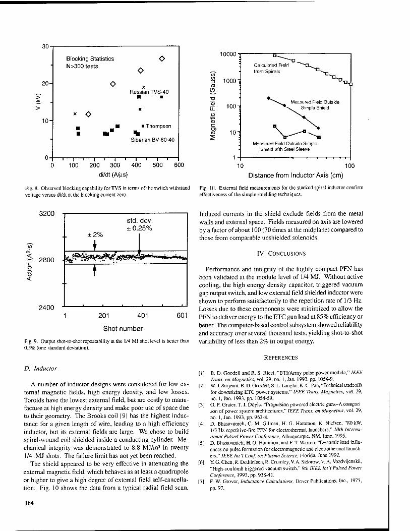
ou-
Blocking Statistics N>300 tests
O O
20- o X Russian TVS-40 ■
10- ■ m
■
■ Thompson ■
Siberian BV-60-40
U-] ■ I > I i i i 1 i 1 i 100 200 300 400
di/dt (A/us)
500 600
to
O
CD c CO
UUUU":
1000]
Calculated Field ^"""O from Spirals ^s_
^1 1001
^^\^ Measured Field Outside ^^. Simple Shield
101 \^^
1 -
Measured Field Outside Simple Shield with Steel Sleeve
1 1 1 1 1—i—i—i—
10 100
Distance from Inductor Axis (cm)
Fig. 8. Observed blocking capability for TVS in terms of the switch withstand Fig. 10. External field measurements for the stacked spiral inductor confirm voltage versus di/dt at the blocking current zero. effectiveness of the simple shielding techniques.
3200
< c o o <
2800
2400 201 401
Shot number
601
Fig. 9. Output shot-to-shot repeatability at the 1/4 MJ shot level is better than 0.5% (one standard deviation).
D. Inductor
A number of inductor designs were considered for low ex- ternal magnetic fields, high energy density, and low losses. Toroids have the lowest external field, but are costly to manu- facture at high energy density and make poor use of space due to their geometry. The Brooks coil [9] has the highest induc- tance for a given length of wire, leading to a high efficiency inductor, but its external fields are large. We chose to build spiral-wound coil shielded inside a conducting cylinder. Me- chanical integrity was demonstrated to 8.8 MJ/m3 in twenty 1/4 MJ shots. The failure limit has not yet been reached.
The shield appeared to be very effective in attenuating the external magnetic field, which behaves as at least a quadrupole or higher to give a high degree of external field self-cancella- tion. Fig. 10 shows the data from a typical radial field scan.
Induced currents in the shield exclude fields from the metal walls and external space. Fields measured on axis are lowered by a factor of about 100 (70 times at the midplane) compared to those from comparable unshielded solenoids.
IV. CONCLUSIONS
Performance and integrity of the highly compact PFN has been validated at the module level of 1/4 MJ. Without active cooling, the high energy density capacitor, triggered vacuum gap output switch, and low external field shielded inductor were shown to perform satisfactorily to the repetition rate of 1/3 Hz. Losses due to these components were minimized to allow the PFN to deliver energy to the ETC gun load at 85% efficiency or better. The computer-based control subsystem showed reliability and accuracy over several thousand tests, yielding shot-to-shot variability of less than 2% in output energy.
REFERENCES
[1] B. D. Goodcll and R. S. Ricci, "BTI/Army pulse power module," IEEE Trans, on Magnetics, vol. 29, no. 1, Jan. 1993, pp. 1054-9.
[2] W. J. Sarjeant, B. D. Goodcll, S. L. Langlic, K. C. Pan, "Technical tradeoffs for downsizing ETC power systems," IEEE Trans. Magnetics, vol. 29, no. l.Jan. 1993, pp. 1054-59.
[3] G. F. Grater, T. J. Doyle, "Propulsion powered electric guns-A compari- son of power system architectures," IEEE Trans, on Magnetics, vol. 29, no. l,Jan. 1993, pp. 963-8.
[4] D. Bhasavanich, C. M. Gilman, H. G. Hammon, K. Nielsen, "80 kW, 1/3 Hz rcpclitivc-firc PFN for electrothermal launchers," 10th Interna- tional Pulsed Power Conference, Albuquerque, NM, June, 1995.
[5] D. Bhasavanich, H. G. Hammon, and F. T. Warren, "Dynamic load influ- ences on pulse formation for electromagnetic and electrothermal launch- ers," IEEE Int 7 Conf. on Plasma Science, Florida, June 1992.
[6] Y. G. Chen, R. Dcthlcfscn, R. Crumley, V. A. Sidorow, V. A. Vozdvijcnskii, "High-coulomb triggered vacuum switch," 9th IEEE Int'I Pulsed Power Conference, 1993, pp. 938-41.
[7] F. W. Grovcr, Inductance Calculations, Dover Publications, Inc., 1973, pp. 97.
164
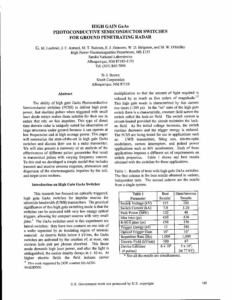
HIGH GAIN GaAs PHOTOCONDUCTIVE SEMICONDUCTOR SWITCHES
FOR GROUND PENETRATING RADAR
G. M. Loubriel, J. F. Aurand, M. T. Buttram, F. J. Zutavern, W. D. Helgeson, and M. W. O'Malley High Power Electromagnetics Department, MS 1153
Sandia National Laboratories Albuquerque, NM 87185-1153
Tel. (505) 845-7096
D. J. Brown Ktech Corporation
Albuquerque, NM 87110
Abstract
The ability of high gain GaAs Photoconductive Semiconductor switches (PCSS) to deliver high peak power, fast risetime pulses when triggered with small laser diode arrays makes them suitable for their use in radars that rely on fast impulses. This type of direct time domain radar is uniquely suited for observation of large structures under ground because it can operate at low frequencies and at high average power. This paper will summarize the state-of-the-art in high gain GaAs switches and discuss their use in a radar transmitter. We will also present a summary of an analysis of the effectiveness of different pulser geometries that result in transmitted pulses with varying frequency content. To this end we developed a simple model that includes transmit and receive antenna response, attenuation and dispersion of the electromagnetic impulses by the soil, and target cross sections.
Introduction on High Gain GaAs Switches
This research has focused on optically triggered, high gain GaAs switches for impulse sources for ultrawide bandwidth (UWB) transmitters. The practical significance of this high gain switching mode is that the switches can be activated with very low energy optical triggers, allowing for compact sources with very small jitter.1 The GaAs switches used in this experiment are lateral switches: they have two contacts on one side of a wafer separated by an insulating region of intrinsic material. At electric fields below 4 kV/cm, the GaAs switches are activated by the creation of, at most, one electron hole pair per photon absorbed. This linear mode demands high laser power, and after the light is extinguished, the carrier density decays in 1- 10 ns. At higher electric fields the field induces carrier
* This work supported by DOE contract DE-AC04- 94AL85000.
multiplication so that the amount of light required is reduced by as much as five orders of magnitude. ' This high gain mode is characterized by fast current rise times (-200 ps). In the "on" state of the high gain switch there is a characteristic, constant field across the switch called the lock-on field. The switch current is circuit-limited provided the circuit maintains the lock- on field. As the initial voltage increases, the switch risetime decreases and the trigger energy is reduced. The PCSS are being tested for use in applications such as: UWB transmitters, firing sets, electro-optic modulators, current interrupters, and pulsed power applications such as MV accelerators. Each of these applications imposes a different set of requirements on switch properties. Table 1 shows our best results obtained with the switches for these applications.
Table 1. Results of tests with high gain GaAs switches. The first column is the best results obtained in various, independent tests. The second column are the results from a single system.
Table I Parameter
Best Results*
Simultaneous Results
Switch Voltage (kV) 155 100 Switch Current (kA) 7.0 1.26 Peak Power (MW) 120 48 Rise time (ps) 430 430 R-M-S jitter (ps) 150 150 Trigger Energy (nJ) 13 180
Optical Trigger Gain 105 105
Repetition Rate (Hz) 1,000 1,000 Electric Field (kV/cm) 100 67 Device Lifetime (# pulses)
6xl06 5 x 10⁴, (at 77 kV)
* Not all the results are simultaneous.
U.S. Government work not protected by U.S. copyright 165
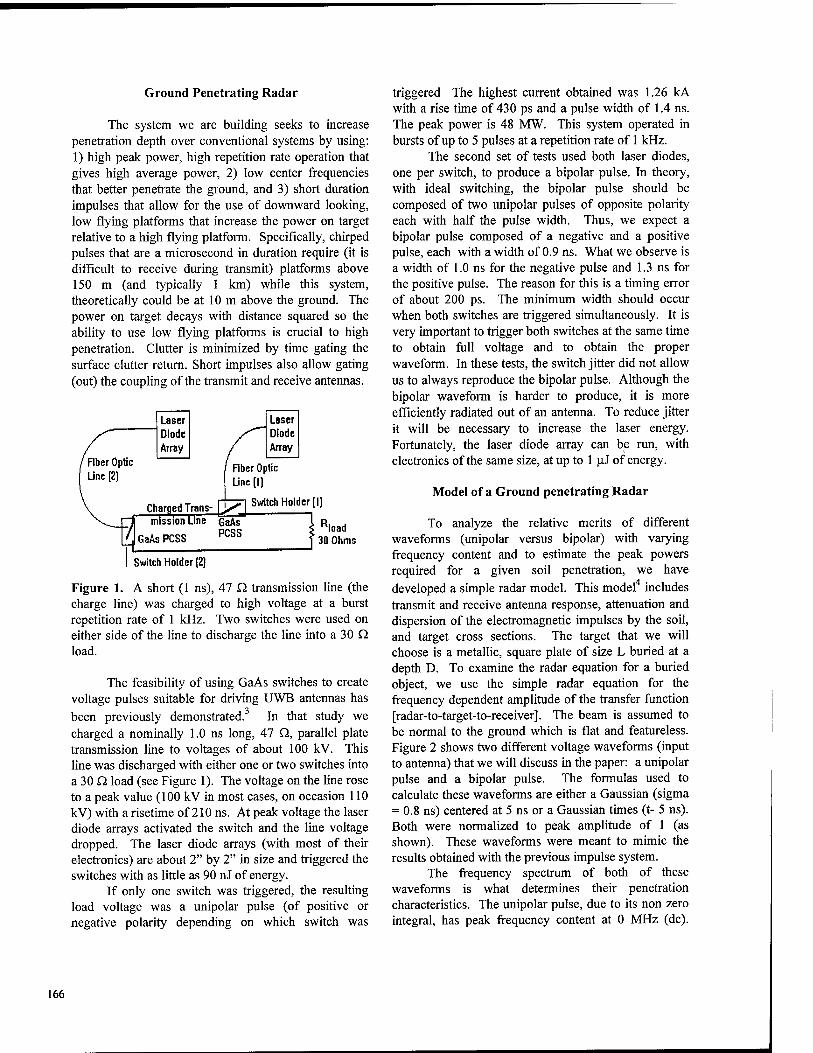
Ground Penetrating Radar
The system we are building seeks to increase penetration depth over conventional systems by using: 1) high peak power, high repetition rate operation that gives high average power, 2) low center frequencies that better penetrate the ground, and 3) short duration impulses that allow for the use of downward looking, low flying platforms that increase the power on target relative to a high flying platform. Specifically, chirped pulses that are a microsecond in duration require (it is difficult to receive during transmit) platforms above 150 m (and typically 1 km) while this system, theoretically could be at 10 m above the ground. The power on target decays with distance squared so the ability to use low flying platforms is crucial to high penetration. Clutter is minimized by time gating the surface clutter return. Short impulses also allow gating (out) the coupling of the transmit and receive antennas.
Charged Trans- _T mission Line
', GaAs PCSS
Fiber Optic Line (I)
Switch Holder (I]
GaAs PCSS } "load
30 Ohms
I Switch Holder [2)
Figure 1. A short (1 ns), 47 Q transmission line (the charge line) was charged to high voltage at a burst repetition rate of 1 kHz. Two switches were used on either side of the line to discharge the line into a 30 Q load.
The feasibility of using GaAs switches to create voltage pulses suitable for driving UWB antennas has been previously demonstrated. In that study we charged a nominally 1.0 ns long, 47 Q, parallel plate transmission line to voltages of about 100 kV. This line was discharged with either one or two switches into a 30 Q load (see Figure 1). The voltage on the line rose to a peak value (100 kV in most cases, on occasion 110 kV) with a risetime of 210 ns. At peak voltage the laser diode arrays activated the switch and the line voltage dropped. The laser diode arrays (with most of their electronics) are about 2" by 2" in size and triggered the switches with as little as 90 nJ of energy.
If only one switch was triggered, the resulting load voltage was a unipolar pulse (of positive or negative polarity depending on which switch was
triggered The highest current obtained was 1.26 kA with a rise time of 430 ps and a pulse width of 1.4 ns. The peak power is 48 MW. This system operated in bursts of up to 5 pulses at a repetition rate of 1 kHz.
The second set of tests used both laser diodes, one per switch, to produce a bipolar pulse. In theory, with ideal switching, the bipolar pulse should be composed of two unipolar pulses of opposite polarity each with half the pulse width. Thus, we expect a bipolar pulse composed of a negative and a positive pulse, each with a width of 0.9 ns. What we observe is a width of 1.0 ns for the negative pulse and 1.3 ns for the positive pulse. The reason for this is a timing error of about 200 ps. The minimum width should occur when both switches are triggered simultaneously. It is very important to trigger both switches at the same time to obtain full voltage and to obtain the proper waveform. In these tests, the switch jitter did not allow us to always reproduce the bipolar pulse. Although the bipolar waveform is harder to produce, it is more efficiently radiated out of an antenna. To reduce jitter it will be necessary to increase the laser energy. Fortunately, the laser diode array can be run, with electronics of the same size, at up to 1 uJ of energy.
Model of a Ground penetrating Radar
To analyze the relative merits of different waveforms (unipolar versus bipolar) with varying frequency content and to estimate the peak powers required for a given soil penetration, we have developed a simple radar model. This model includes transmit and receive antenna response, attenuation and dispersion of the electromagnetic impulses by the soil, and target cross sections. The target that we will choose is a metallic, square plate of size L buried at a depth D. To examine the radar equation for a buried object, we use the simple radar equation for the frequency dependent amplitude of the transfer function [radar-to-target-to-receiver]. The beam is assumed to be normal to the ground which is flat and featureless. Figure 2 shows two different voltage waveforms (input to antenna) that we will discuss in the paper: a unipolar pulse and a bipolar pulse. The formulas used to calculate these waveforms are either a Gaussian (sigma = 0.8 ns) centered at 5 ns or a Gaussian times (t- 5 ns). Both were normalized to peak amplitude of 1 (as shown). These waveforms were meant to mimic the results obtained with the previous impulse system.
The frequency spectrum of both of these waveforms is what determines their penetration characteristics. The unipolar pulse, due to its non zero integral, has peak frequency content at 0 MHz (dc).
166
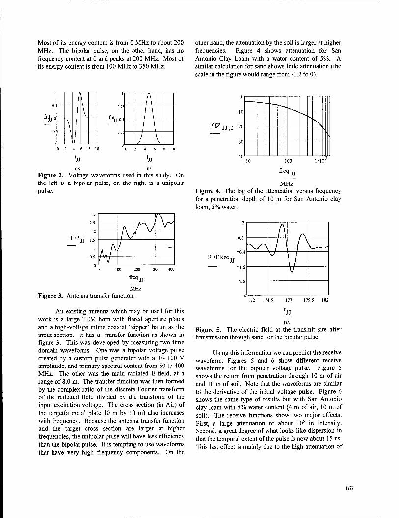
Most of its energy content is from 0 MHz to about 200 MHz. The bipolar pulse, on the other hand, has no frequency content at 0 and peaks at 200 MHz. Most of its energy content is from 100 MHz to 350 MHz.
■ other hand, the attenuation by the soil is larger at higher frequencies. Figure 4 shows attenuation for San Antonio Clay Loam with a water content of 5%. A similar calculation for sand shows little attenuation (the scale in the figure would range from -1.2 to 0).
0.;
feJjo
\
i
0.7!
02'.
0
A V l\
\ \
-■
\ V 0 2 4 6
UJJ 1j ns ns
Figure 2. Voltage waveforms used in this study. On the left is a bipolar pulse, on the right is a unipolar pulse.
3
'\ *• V*
|TFPTT| ,, JJ !-5
0 100 200
freq 300
JJ MHz
Figure 3. Antenna transfer function.
An existing antenna which may be used for this work is a large TEM horn with flared aperture plates and a high-voltage inline coaxial 'zipper' balun as the input section. It has a transfer function as shown in figure 3. This was developed by measuring two time domain waveforms. One was a bipolar voltage pulse created by a custom pulse generator with a +/- 100 V amplitude, and primary spectral content from 50 to 400 MHz. The other was the main radiated E-field, at a range of 8.0 m. The transfer function was then formed by the complex ratio of the discrete Fourier transform of the radiated field divided by the transform of the input excitation voltage. The cross section (in Air) of the target(a metal plate 10 m by 10 m) also increases with frequency. Because the antenna transfer function and the target cross section are larger at higher frequencies, the unipolar pulse will have less efficiency than the bipolar pulse. It is tempting to use waveforms that have very high frequency components. On the
loga
-io
JJ.3-20
-30
-40 , ,„3 10 100
freq
1-10
JJ
MHz Figure 4. The log of the attenuation versus frequency for a penetration depth of 10 m for San Antonio clay loam, 5% water.
REERec
Figure 5. The electric field at the transmit site after transmission through sand for the bipolar pulse.
Using this information we can predict the receive waveform. Figures 5 and 6 show different receive waveforms for the bipolar voltage pulse. Figure 5 shows the return from penetration through 10 m of air and 10 m of soil. Note that the waveforms are similar to* the derivative of the initial voltage pulse. Figure 6 shows the same type of results but with San Antonio clay loam with 5% water content (4 m of air, 10 m of soil). The receive functions show two major effects. First, a large attenuation of about 105 in intensity. Second, a great degree of what looks like dispersion in that the temporal extent of the pulse is now about 15 ns. This last effect is mainly due to the high attenuation of
167
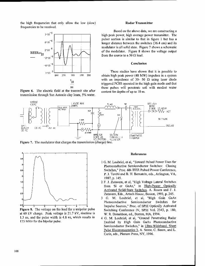
the high frequencies that only allow the low (slow) frequencies to be received.
1-10
6-10
REERei 2-10
:CTJ -2-10
-6-10
-1M0 -5
160 170 180 190 200
ns Figure 6. The electric field at the transmit site after transmission through San Antonio clay loam, 5% water.
Radar Transmitter
Based on the above data, we are constructing a high peak power, high average power transmitter. The pulser section is similar to that in figure 1 but has a longer distance between the switches (36.4 cm) and its modulator is all solid state. Figure 7 shows a schematic of the modulator. Figure 8 shows the voltage output from the source to a 50 Q load.
Conclusion
These studies have shown that it is possible to obtain high peak power (48 MW) impulses in a system with an impedance of 30- 50 Q using laser diode triggered PCSS operated in the high gain mode and that these pulses will penetrate soil with modest water content for depths of up to 10 m.
WALL OUTLET 110 AC 110 AC
(120 KV> DIGDE STACK 1.5 KDHM
OmMAAr HGT
707 AC GROUND
<-mw AMMETER SILICON STANGENESS (USED AS CONTROLLED rlrnnMER VOLTMETER) RECTIFIER
Figure 7. The modulator that charges the transmission (charge) line.
"0 1 2 3 4 5
Figure 8. The voltage on the load for a unipolar pulse at 60 kV charge. Peak voltage is 21.7 kV, risetime is 1.3 ns, and the pulse width is 4.8 ns, which results in 175 MHz for the bipolar pulse.
References
1 G. M. Loubriel, et al, "Toward Pulsed Power Uses for Photoconductive Semiconductor Switches: Closing Switches," Proc. 6th IEEE Pulsed Power Conference, P. J. Turchi and B. H. Bernstein, eds., Arlington, VA, 1987, p. 145.
2 F. J. Zutavera, et al, "High Voltage Lateral Switches from Si or GaAs," in High-Power Optically Activated Solid-State Switches, A. Rosen and F. J. Zutavern, Eds., Artech House, Boston, 1993, p. 245.
3 G. M. Loubriel, et al, "High Gain GaAs Photoconductive Semiconductor Switches for Impulse Sources," Proc. of SPIE Optically Activated Switching Conference IV, SPIE Vol. 2343, p. 180, W. R. Donaldson, ed., Boston, MA, 1994.
4 G. M. Loubriel, et al, "Ground Penetrating Radar Enabled by High Gain GaAs Photoconductive Semiconductor Switches," in Ultra-Wideband, Short Pulse Electromagnetics 3, A. Stone, C. Baum, and L. Carin, eds., Plenum Press, NY, 1996.
168
Electrical Noise Cancellation Using High Temperature Superconductor Modulation
J. Dvorak, W. Hodges, C. Braun Division of Engineering, Colorado School of Mines, Golden Colorado 80401
Abstract
A hybrid fault current limiter and active noise cancellation system is being developed at the Colorado School of Mines for use in high voltage DC power systems with very high SNR requirements, such as those found in radar systems. This system uses a re- sistive superconducting fault current limiter (FCL) and electrically isolated solenoid to produce a variable re- sistance across a length of bulk high Tc superconduct- ing YBCO filament. This paper describes the process of material testing of the YBCO filaments, modeling, and modulator prototype development. Results from the material testing and modeling are also presented.
Introduction
Fault current limiters are one new application of high Tc superconducting materials.[l,2,3] The most common configuration is a variable inductance ap- proach for utility AC systems. A fault current causes a transition from superconducting to normal that drasti- cally raises the inductance of a faulted circuit and lim- its the short circuit current. [4,5] However, these AC inductive FCL are not applicable to DC systems.
The work described here uses a resistive current limiting to minimize short circuit currents. A tube- based radar system would be one example of a DC system that would benefit from such a system. Inclu- sion of a superconducting FCL would protect the radar tube from complete failure if an arc developed. Given this FCL, it is a natural step to consider actively modulating the FCL for noise cancellation at the load.
Requirements for radar system, such as mV ripple from a lOkV DC power supply, pose serious engineer- ing difficulties. These systems typically use a low-side switching power supply that is transformed to high voltage, rectified and filtered. A combination of a higher ripple/low cost DC power supply along with a modulated FCL may lead to superior overall system. Using the periodic nature of the noise signal, the FCL can be modulated to actively cancel the last bit of un- wanted signal components (mVs) as well as serving as a fault protection unit.
Current
Figure 1. The resistance of the superconductor fila- ment depends upon both the current in the filament
and the external magnetic field.
Material Testing Apparatus The system being developed is based on a high
temperature YBCO superconductor produced by Illi- nois Superconductor Corporation (ISC). The filaments are produced in a ceramic extrusion process, and measure 0.76 mm diameter by 190 mm length. The room temperature resistance of a filament is 2.0 Q. At cryogenic temperatures, the resistance of the supercon- ductor is a function of temperature, current density, external magnetic field and other physical parameters. The relationship between current density, magnetic field, and resistance, is critical for this modulator.
The ceramic fibers developed are made from bulk, sintered YBCO ceramic[6] and are very different from the thin film superconductors. These filaments show a characteristic resistance similar to the graph shown in Figure 1. At zero current, the superconductor would have negligible electrical losses. At high magnetic fields, the resistance of the filament would saturate. In-between there is a linear region which is used to produce controlled modulation.
A testing apparatus was developed for measuring the resistance of the sample while varying the current through the fiber and the current in a coil around the superconductor (see Figure 2). From the measured cur- rents, the current density and external magnetic field could be calculated. The coils used were made by turning magnet wire on a form and then mounting to a circuit board with the power and sensing connections.
0-7803-3076-5/96/S5.00 © 1996 IEEE 169
GPBMmfa«
Figure 2. Measurement System Diagram for determining proprieties of YBCO material
A program was written in Visual Basic to control the test equipment and automate the data collection. Data was graphed in real time, as well as exported to Microsoft Excel for further analysis. Results of this experiment are discussed later.
Numerical Modeling
In order to better understand the operation and potential problems with this modulation scheme, we have developed a numerical model of the modulation system as shown in Figure 3. Here we see a voltage source with an induce noise signal. This is fed into the HTSC modulator and the load. The field coil control- ler monitors the voltage on the load and compensates for any deviations from the desired voltage by adjusting the current into the field coil. This field coil current produces a magnetic field that alters the resistance of the superconductor which changes the voltage on the load. A graph of the operation is shown on Figure 6.
Voltage Source, Volts
DC Source + Periodic Ripple Voltage
¥W^r r™~\ Load +
HTSC Modulator
Field Current,, x^*
Mux
Mux
a Source and
Load voltages
Load voltage, V
HTSC Field Coil Controller
Figure 4. A Simulink/Matlab simulation block diagram for the HTSC Modulator system. Inside each of the
major blocks is a detailed sub-module.
Modulator Apparatus
Based on the numerical model described above, a modulator apparatus was developed to conduct the experimentation. The setup uses the same dewar and material, however, different control and measurement hardware was necessary to satisfy the time based characteristics of the noise and cancellation signal.
A comparison of the measurement system and noise cancellation systems (Figures 2 and 4) show the similar core equipment, however, rather than utiliz- ing high accuracy DC equipment, the control system uses a data acquisition card and arbitrary waveform generator (AWG) to interact with the superconductor.
An adaptive, rule based pattern matching feed- back control algorithm is being considered to control the coil current based on the noise measured on a
Figure 3. Control System Diagram for the HTSC Active Noise Modulator.
resistive load. This error signal is matched to various patterns stored in the computers memory. This allows the computer to determine the mode of operation of a power supply and, based on previous measurements, deliver a control signal to cancel the noise.
The control signal is output to the AWG which is ;ed to produce a high-speed, synchronous cancellation gnal. From the AWG this signal goes into a current nplifier and then to the field coil wrapped around the iperconductor filament. Thus the cancellation signal ives the magnetic field of the field coil and modu- tes the resistance of the HTSC fiber.
Currently, the system utilizes an external clock to ■nch the noise production and data collection. Even- ally, intelligence could be developed in the control ructure to allow unsynchronized operation of the
noise cancellation system.
170
Material testing results Initial superconducting samples have been tested
with varied results. Some of the samples have exhibited some of the features expected from Figure 1. However, due to thermal and power supply limitations, we have not been able to fully saturate the resistance of a sam- ple.
As shown in Figure 5, the resistance of the super- conducting fiber dramatically changes as a function of external magnetic field modulation. However, anoma- lies in the data, perhaps caused by a heating effect, have created an additional ripple variation in the re- sistance This sharp transition may be a result of a tran- sition between point and plane boiling in the liquid nitrogen bath.
Volt:
5.5
5
4.5
Figure 5. Sample 2-1 resistance as a function of self and field coil currents.
The maximum modulation in the filament's resis- tance was from 0.05Q to 0.20C1 while carrying 5 amps. This would be sufficient to cancel up to 0.75 volts of noise.
Modeling results Shown on Figure 6 is the input voltage DC source
+ AC ripple. A 60Hz sinusoid source is used to repre- sent the noise of a switching power supply. This is also the way the first set of experiments will show that active cancellation is feasible. With only a simple control strategy the overall ripple was reduced by over a factor of 100 going from 0.4 Vpp to under 4 mVpp.
3.5
DC Source + AC ripple (0.4 Vpp)
%^ßi^mj h Load voltage, after noise
cancellation (4 mVpp)
0.1 0 0.02 0.04 0.06 0.08 Time (seconds)
Figure 6. Simulation results of the HTSC Modulator. The top trace is the DC source + AC ripple. The lower
trace is the voltage at the load after the modulator.
Experimental results
Figure 7. The experimental setup monitoring and control systems are above the computer and LN2 dewar
holding the HTSC fiber.
We plan to start with a low frequency demonstra- tor, due to the limitations in data acquisition and con- trol. Then as our predictive algorithms and fast control systems are developed, we will be able to scale up to frequencies in the range of switching power supplies.
171
At this time, further work is necessary in the char- acterization of the superconducting filaments. In addi- tion to accurate measurement of their DC resistance values, the inductance of the samples must also be measured to determine the operational frequency limit. The coil geometry must be optimized to produce the highest field while producing the smallest amount of Joule heating. In addition, the thermal limits of opera- tion for the system must be determined.
Conclusions High temperature, bulk-sintered superconducting
fibers are suitable for use as a resistive fault current limiter for DC applications. In addition, the resistance of these same fibers can be externally modulated. One application of this effect is to create a noise cancella- tion modulator. This allows a magnetically isolated modulation of the high voltage side of a DC power supply at the same time as providing a fault current limiter.
We have developed an experimental apparatus to characterize the resistance of these fibers. This data has been used in our simulations to demonstrate the feasibility of noise cancellation. The next step is to finish the experimental setup for the HTSC Modulator and gather data.
Acknowledgments This work is supported by Illinois Superconductor
Corporation and the National Science Foundation
1 Thurles, E., "Towards the Superconducting Fault Current Limiter." IEEE Trans, on Power Deliv- ery. Vol. 6 No. 2: Apr 1991. 801.
2 Slade, P. "The Utility Requirements for a Distri- bution Fault Current Limiter" IEEE Trans, on Power Delivery. Vol 7 No 2 Apr 1992 507.
3 Acero, J. "Current Limiter Based on Melt Proc- essed YBCO Bulk Superconductors." IEEE Trans, on Applied Superconductivity. Vol 5 No 2 June 1995. 1071.
4 Hara, T. "Superconducting Fault Current Lim- iter Development." IEEE Trans, on Magnetics. Vol 27 No 2 Mar 1991. 2345.
5 Fleishman, L. "Design Considerations for an In- ductive High Tc Superconducting Fault Current Lim- iter." IEEE Trans, on Applied Superconductivity. Vol 3 No 1. Mar 1993. 570.
6 Hodge, James D. " A Self-Restoring Fault Cur- rent Limiter Utilizing High Temperature Supercon- ductor Components." Illinois Superconductor Corporation. SBIR Phase II Proposal. Jan 1992.
172
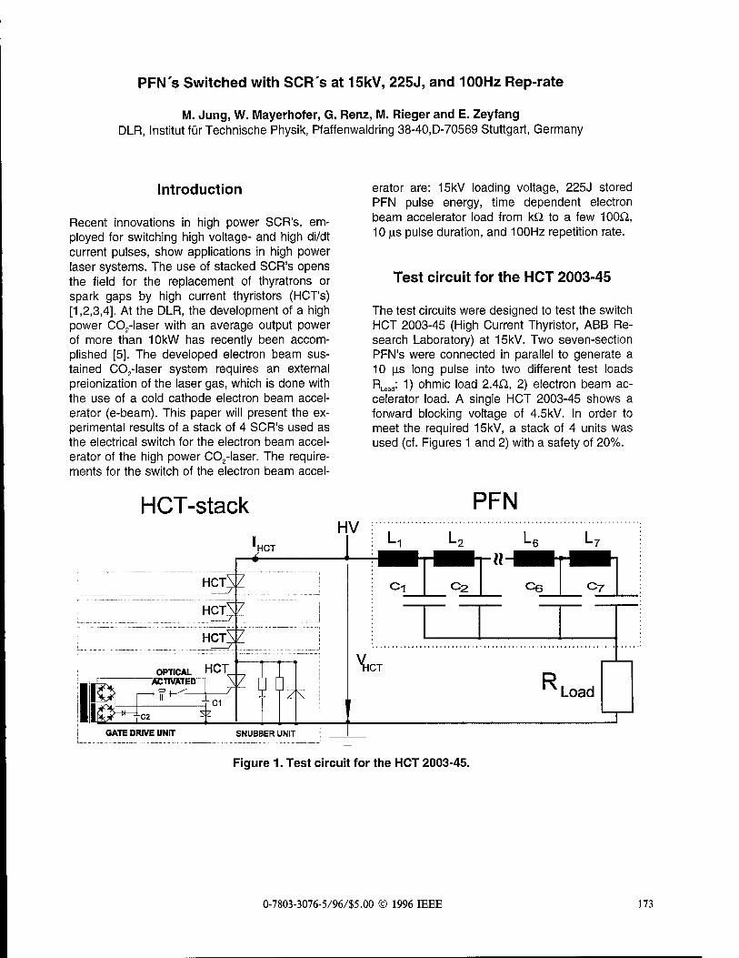
PFN's Switched with SCR's at 15kV, 225 J, and 100Hz Rep-rate
M. Jung, W. Mayerhofer, G. Renz, M. Rieger and E. Zeyfang DLR, Institut für Technische Physik, Pfaffenwaldring 38-40,D-70569 Stuttgart, Germany
Introduction
Recent innovations in high power SCR's, em- ployed for switching high voltage- and high di/dt current pulses, show applications in high power laser systems. The use of stacked SCR's opens the field for the replacement of thyratrons or spark gaps by high current thyristors (HCT's) [1,2,3,4]. At the DLR, the development of a high power C02-laser with an average output power of more than 10kW has recently been accom- plished [5]. The developed electron beam sus- tained C02-laser system requires an external preionization of the laser gas, which is done with the use of a cold cathode electron beam accel- erator (e-beam). This paper will present the ex- perimental results of a stack of 4 SCR's used as the electrical switch for the electron beam accel- erator of the high power C02-laser. The require- ments for the switch of the electron beam accel-
HCT-stack HV
"HCT
HCTV
HCTV
HCT^Z
erator are: 15kV loading voltage, 225J stored PFN pulse energy, time dependent electron beam accelerator load from k£2 to a few 100Q, 10 u.s pulse duration, and 100Hz repetition rate.
Test circuit for the HCT 2003-45
The test circuits were designed to test the switch HCT 2003-45 (High Current Thyristor, ABB Re- search Laboratory) at 15kV. Two seven-section PFN's were connected in parallel to generate a 10 u.s long pulse into two different test loads RLoad: 1) ohmic load 2AD., 2) electron beam ac- celerator load. A single HCT 2003-45 shows a forward blocking voltage of 4.5kV. In order to meet the required 15kV, a stack of 4 units was used (cf. Figures 1 and 2) with a safety of 20%.
PFN
; c-,
v HCT
R Load
GATE DRIVE UNIT SNUBBER UNIT
Figure 1. Test circuit for the HCT 2003-45.
0-7803-3076-5/96/55.00 © 1996 IEEE 173
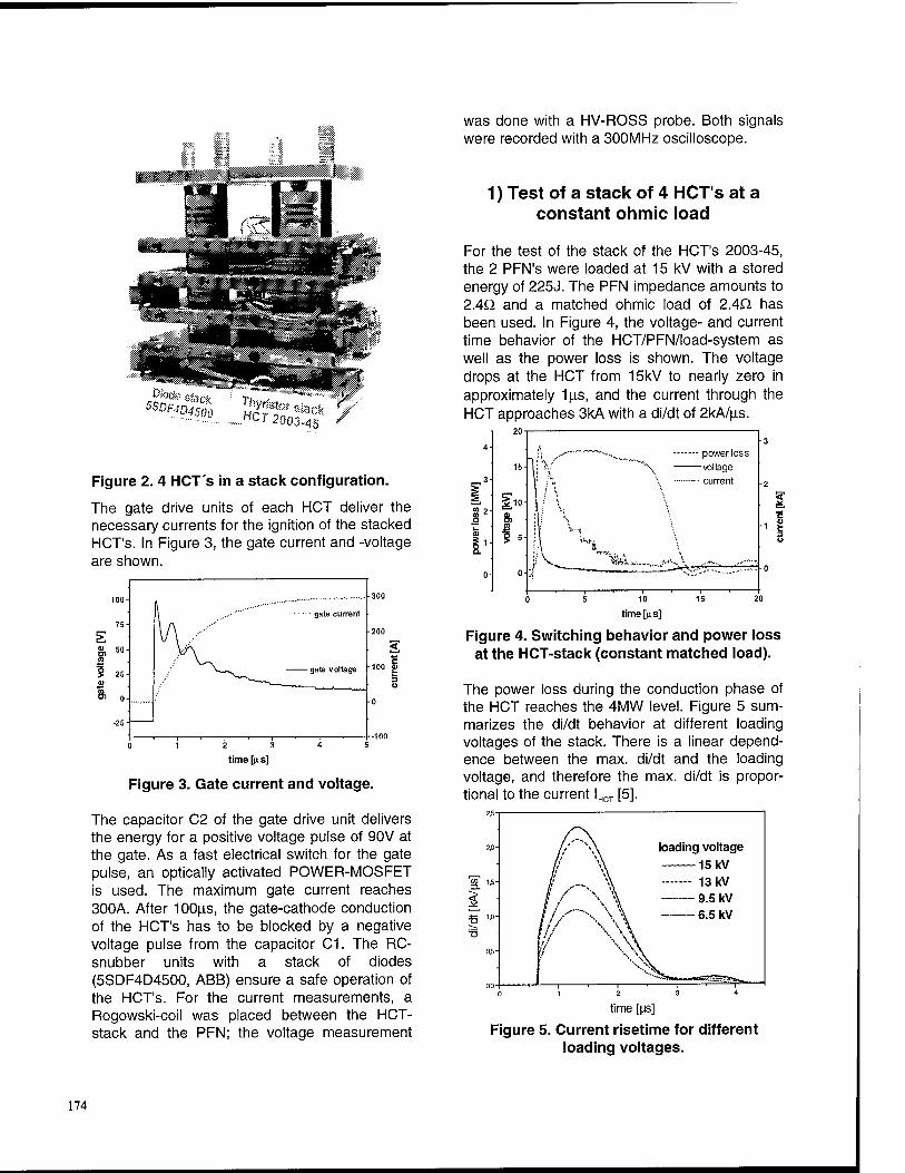
was done with a HV-ROSS probe. Both signals were recorded with a 300MHz oscilloscope.
Figure 2. 4 HCT's in a stack configuration.
The gate drive units of each HCT deliver the necessary currents for the ignition of the stacked HCT's. In Figure 3, the gate current and -voltage are shown.
100-
75- \ A
s \J\ /" & 50- CO
% 25- V^v. gate voltage "
0) ^—, _.. o> o-
■
1 1 1 1 1 1 1 1 1
100 0)
3
time [n s]
Figure 3. Gate current and voltage.
The capacitor C2 of the gate drive unit delivers the energy for a positive voltage pulse of 90V at the gate. As a fast electrical switch for the gate pulse, an optically activated POWER-MOSFET is used. The maximum gate current reaches 300A. After 100u.s, the gate-cathode conduction of the HCT's has to be blocked by a negative voltage pulse from the capacitor C1. The RC- snubber units with a stack of diodes (5SDF4D4500, ABB) ensure a safe operation of the HCT's. For the current measurements, a Rogowski-coil was placed between the HCT- stack and the PFN; the voltage measurement
1) Test of a stack of 4 HCT's at a constant ohmic load
For the test of the stack of the HCT's 2003-45, the 2 PFN's were loaded at 15 kV with a stored energy of 225J. The PFN impedance amounts to 2AQ. and a matched ohmic load of 2AQ. has been used. In Figure 4, the voltage- and current time behavior of the HCT/PFN/load-system as well as the power loss is shown. The voltage drops at the HCT from 15kV to nearly zero in approximately 1ns, and the current through the HCT approaches 3kA with a di/dt of 2kA/^s.
- power loss -voltage • current
WÄ..V,-..,.
time [(is]
Figure 4. Switching behavior and power loss at the HCT-stack (constant matched load).
The power loss during the conduction phase of the HCT reaches the 4MW level. Figure 5 sum- marizes the di/dt behavior at different loading voltages of the stack. There is a linear depend- ence between the max. di/dt and the loading voltage, and therefore the max. di/dt is propor- tional to the current
time [\s]
Figure 5. Current risetime for different loading voltages.
174
In Figure 6, 2 pulses out of a sequence of 100 shots are shown.
£i.
-#-
r\
voltage — current
r\
^J, v
K~M*r, F "7^-o ■#-
shot#
Figure 6. Switching behavior in repetitively pulsed operation, 1st and 10th shots in a
burst of 100 shots at 100Hz.
The current pulses through the HCT-stack of max. 3kA show a good reproducibility from shot to shot. In contrast to an earlier work [5], the max. current has been reduced from 7 to 3kA due to the matched higher ohmic load of 2AQ.. This shows that the HCT-stack is not operated at the max. rating of the HCT.
2) Test of a stack of 4 HCT's at an electron beam accelerator load
The electron beam accelerator system consists of a power supply unit (30kV, 120kJ/s), the HCT stack, a modulator (PFN max. 30kV, 7.5kA, 10kA/us, lOps, 1kJ/shot) and the load.
A parallel and a series resistance of Rp = 100Q and Rs = 0.6Q. is installed. The pulse transformer has a ratio of 1:10 (cf. Fig. 7). Between the transformer and the e-beam, there is an HV- connection cable (100pF/m). The voltage at the e-beam cathode can be varied between 100 and 230kV at the peak. The e-beam window dimen- sion is 20 x 200 cm2, and the electron beam current density ranges between 10 and 100 mA/cm2. The voltage and current wave forms measured at the HCT-stack as well as the power loss is displayed in Fig. 8.
5
4-
E w1 2 (A O >- 1 a> 3 o o
14-
12 . ■' '._ voltage
10- current 8-
6- I
I
'■.- ■.
4- J V
2-
0- tM:
1e
- 0
10 15
time [us]
20
Figure 8. Switching behavior and power loss at the HCT-stack (e-beam-load).
Since the e-beam load shows a strong time de- pendent resistance ranging from 1.5kfi to approximately 0.3k£2, the current exhibits a strong time dependence as well. Figure 9 shows a close-up of the conduction phase of the HCT- stack. Compared to the pure ohmic load case, the power loss falls off in a much shorter time (500ns).
:10 T T I°iri e-beam modulator MRP II
HV
c '! f t % c10
ie so
4 main discharge modulators
I Figure 9. Close-up of the HCT-stack current and di/dt-curve for an e-beam load.
Figure 7. Electrical concept of the laser sy- stem.
175
In Figure 10, a sequence of 8 pulses out of a burst of 100 pulses is shown. The upper curves display the HCT current and voltage and the lower curves show the current and voltage at the secondary side of the pulse transformer. The e- beam accelerator has been run at 100Hz with the 10kW C02-laser in operation. In a future work it is planed to increase the number of HCTs to reach a switching voltage of 30kV.
r—, 16
5 Ü X
CD CO CO
■I-*
o >
10
^ta_ if**"1 k*-
*■
l^""" ir*- r- r-
2 J 4 97 98 99 100 shot#
Summary
A stack of 4 High Current Thyristors (HCT 2003- 45, ABB) has been tested as an HV-switch at a constant ohmic and a dynamic (electron beam accelerator) load. The loading voltage of the PFN's was 15kV with a stored energy of 225J per pulse. The electron beam accelerator (200kV) together with the 10kW-CO2-laser was operated at 100Hz. The stack of high current thyristors operated reliably during the test phase.
References
[1] M. Jung, W. Mayerhofer, M. Edele, O. Gstir, Th. Schweizer, E. Zeyfang, and E. Rame- zani, 'Test of fast SCR's as spark gap replace- ment', 10th IEEE Pulsed Power Conf., Albu- querque (1995).
[2] L.E. Kingsley, R. Pastore, H. Singh, G. Ayres, R. Burdalski, and J. F. Agee, 'Solid-state power switches for HPM modulators', 10th IEEE Pulsed Power Conf., Albuquerque (1995).
[3] G.J. Rohwein, L.D. Roose, and W.M. Portnoy, 'Characterization of high power thyri- stors', 10th IEEE Pulsed Power Conf., Albu- querque, NM (1995).
[4] K.F. McDonald, 'Evaluation of solid state switches for a space based laser modulator', 9th IEEE Pulsed Power Conf., p.503, Albuquer- que,NM(1993).
[5] M. Jung, W. Mayerhofer, G. Renz, and E. Zeyfang, 'High power C02-laser at 100Hz rep- rate', 22nd Power Modulator Symposium Conf., Boca Raton, FL(1996).
Figure 10. Current and voltage pulses at the HCT-stack for the e-beam load (8 out of 100 pulses in a burst, 100Hz rep-rate).
176
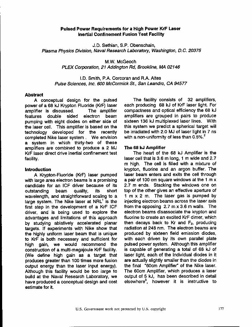
Pulsed Power Requirements for a High Power KrF Laser Inertial Confinement Fusion Test Facility
J.D. Sethian, S.P. Obenschain, Plasma Physics Division, Naval Research Laboratory, Washington, D.C. 20375
M.W. McGeoch PLEX Corporation, 21 Addington Rd, Brookline, MA 02146
I.D. Smith, P.A. Corcoran and R.A. Altes Pulse Sciences, Inc. 600 McCormick St., San Leandro, CA 94577
Abstract A conceptual design for the pulsed
power of a 68 kJ Krypton Fluoride (KrF) laser amplifier is discussed. The amplifier features double sided electron beam pumping with eight diodes on either side of the laser cell. This amplifier is based on the technology developed for the recently completed Nike laser system . We envision a system in which thirty-two of these amplifiers are combined to produce a 2 MJ KrF laser direct drive inertial confinement test facility.
Introduction A Krypton-Fluoride (KrF) laser pumped
with large area electron beams is a promising candidate for an ICF driver because of its outstanding beam quality, its short wavelength, and straightforward scaling to a large system. The Nike laser at NRL1 is the first step in the development of a KrF ICF driver, and is being used to explore the advantages and limitations of this approach by studying ablatively accelerated planar targets. If experiments with Nike show that the highly uniform laser beam that is unique to KrF is both necessary and sufficient for high gain, we would recommend the construction of a multi-megajoule KrF facility. (We define high gain as a target that produces greater than 100 times more fusion output energy than the laser input energy). Although this facility would be too large to build at the Naval Research Laboratory, we have produced a conceptual design and cost estimate for it.
The facility consists of 32 amplifiers, each producing 68 kJ of KrF laser light. For compactness and optical efficiency the 68 kJ amplifiers are grouped in pairs to produce sixteen 136 kJ multiplexed laser lines. With this system we predict a spherical target will be irradiated with 2.0 MJ of laser light in 7 ns with a non-uniformity of less than 0.5%.2
The 68 kJ Amplifier The heart of the 68 kJ Amplifier is the
laser cell that is 3.6 m long, 1 m wide and 2.7 m high. The cell is filled with a mixture of krypton, fluorine and an argon buffer. The laser beam enters and exits the cell through a pair of 100 cm square windows at the 1 m x 2.7 m ends. Stacking the windows one on top of the other gives an effective aperture of 1 m x 2 m. The laser gas is pumped by injecting electron beams across the laser axis from the opposing 2.7 m x 3.6 m walls. The electron beams disassociate the krypton and fluorine to create an excited KrF dimer, which then decays back to Kr and F2, producing radiation at 248 nm. The electron beams are produced by sixteen field emission diodes, with each driven by its own parallel plate pulsed power system. Although this amplifier is capable of generating a total of 68 kJ of laser light, each of the individual diodes in it are actually slightly smaller than the diodes in the final "60cm Amplifier" of the Nike laser. The 60cm Amplifier, which produces a laser output of 5 kJ, has been described in detail elsewhere3, however it is instructive to
U.S. Government work not protected by U.S. copyright 177
compare the parameters of the two systems. This is done in the table below:
the same view for the Nike 60cm Amplifier is shown in the upper portion of the drawing:
60cm Amplifier Nike
(existing)
68 kJ amplifier HIGH GAIN FACILITY (concept}
E-Beam 700 kV, 500 kA 800 kV, 330 kA
Pulse duration (flat top) 240nsec 250 nsec
PFL stored energy/diode 90 kJ 83 kJ
Cathode area 200cmx60cm 100 cm x 48 cm
Cathode current density 42 A/cm2 68 A/cm2
Diodes per amplifier 2 16
Total specific pump power 350 kW/cm3 800 kW/cm3
In most cases the parameters of the 68 kJ amplifier are within 10-20% of that of the Nike 60cm Amplifier. The major difference is the higher specific pump power which is due to both the higher diode power per unit area and an assumed higher energy transmission from cathode into the gas. We achieve the latter by incorporating a new laser cell pressure foil structure based on the "suspension bridge" design conceived and partially tested at Los Alamos4. Even though the pump power is higher it is within the parameters that have been achieved in other systems, some of which have operated at over 1 MW/cm3. (In fact, the smaller 20cm Amplifier of the Nike laser has operated as high as 550 kW/cm3.)
Figure 1 shows the view of the 68 kJ Amplifier from inside the cell, looking into the e-beam diodes on one side. For comparison,
NIKE 60cm AMPLIFIER CATHODE IS 60x200 cm
Circles denote cathode feeds
HIGH GAIN FACILITY 66 kJ AMPLIFIER
CATHODES: 48x100 cm
VIEW WTO E-8EAMO00ES
Figure 1: View inside the laser cell, looking into the electron beam diodes for both the proposed 68 kJ amplifier and the existing Nike 60cm amplifier. The diodes along one wall of the cell are shown. An equal number of diodes line the opposite wall.
Figure 2 shows the top view of the cell, as looking down upon the e-beam diodes. It is in this view that the most unique aspect of this 68 kJ amplifier can be seen: the amplifier is of a "segmented" design, meaning that there are portions of the laser cell that are unpumped (i.e. "missed" by the electron beam). At first glance it was thought that such a design would be severely compromised since the unpumped fluorine, which is a UV absorber, would attenuate so much of the light produced in the pumped regions that the amplifier efficiency would be seriously reduced. However, after carrying out calculations with an experimentally tested KrF amplifier model6, it was determined that this is not the case as the reduction in Amplified Stimulated Emission from the segmentation compensates for the absorption. In addition to laser considerations, such a design allows significant simplification in the pulsed power: 1) the electron beams can be guided in the standard fashion with a simple parallel magnetic field; 2) because the diodes can now be surrounded with return current planes on all four sides, the self field is reduced, the guide field can be relatively low, and the diode closure is reduced; and finally 3), the
178

return current planes reduce the system inductance and hence relax the requirements on the pulsed power.
GUIDE MAGNET
CATHODE
INSULATOR/SWITCH
Figure 2: Top view of the 68 kJ amplifier showing the diodes, insulator/switch assemblies and the guide magnet. Note the "unpumped" regions.
The end view of the laser cell, looking along the path of the laser beam, is shown in Figure 3. This view clearly shows the two 100 cm x 100 cm optical windows that make up the effective optical aperture of 100 cm x 200 cm. Note that comparing Figures 2 and 3 shows the cell is pumped by sixteen separate electron beam diodes.
1.00tm PEAKS*
INSULATOR /SWTCH ASSEMBLIES
waviNrouaR*BH*E
10Ocm x 100 an WINDOWS
TRIGGER LASER OPTICS PATH
Figure 3: End view of the laser cell.
One of the features of this design is that each diode is connected to its own pulse line through two monolithic vacuum insulator sections that contain both the SF6 -insulated switch and the insulating gas around the cathode stalk. The details of this are shown below in Figure 4. The plastic insulator body
is fabricated by casting and/or machining a single piece onto which split metal grading rings are pressed. This arrangement is considerably less expensive than the conventional one in which the switch is located in a separate housing and the insulators and grading rings are individual components that are stacked and held together by external tie rods. This design also substantially decreases the inductance.
Figure 4: Top view of the integrated switch/insulator stack section. There are two of these per cathode.
Although mechanically unconventional, potential plots both before and after switching show that the insulator is graded quite uniformly and the average field is well below the threshold for breakdown.
Each pair of switches (and hence each diode) is fed by a water dielectric rectangular cross section pulse forming line (PFL) of depth 1 m (to correspond the cathode dimension), width 55 cm, and length 5 m (corresponding to a pulse duration of 300 nsec and a flat top duration of 250 nsec). The PFLs are charged to 1.64 MV in 1.8 us by a Marx bank. One Marx charges four PFLs. Each Marx has eleven stages, with two 3.0 u.F capacitors per stage and each stage charged to ± 90 kV.
We have simulated the pulsed power behavior of this amplifier, assuming the anode cathode gap has an initial value of 5.5
179
cm and a closure velocity of 2.3 cm/nsec. Best results are obtained if we assume the diode is driven by a 130 nsec, 1.28 Q pulseline followed with a 20 ns long 1 Q peaker section at the output end of Figure 3. This is very similar to the successful arrangement of the Nike 60 cm Amplifier.3
We found that if the output switches are fired at near peak charge on the waterline, the diode voltage ramps down and the current ramps up by about 6%, averaging 790 kV and 690 kA, respectively, throughout the top part of the pulse. The power to the diode remains almost constant at 54.5 TW ± 2 %. This is more than adequate to meet the laser uniformity requirements.
As said at the outset, we have designed and estimated the cost of an entire 2 MJ laser facility. As part of that effort, we determined that the cost to develop the pulsed power for the 68 kJ amplifier comes out to $20 M for the first unit, where we have allowed a 25% contingency. The cost reduces to about $ 7.1 M in a quantity of 32 for the 2 MJ laser facility. Part of the savings is in the "learning" applied when building a large number of units, and part is due to the fact that a lot of the amplifier subsystems (i.e. gas handling, gas recovery, control systems) would be shared with other components of the facility. The entire cost of the 2 MJ laser facility, including target chamber, all support services, and a 25% contingency, has been estimated to be $950 M. These numbers were obtained with the same algorithms used in costing previous LMF designs7, the NIF8, and other large pulsed power systems,9 as well as experience in building the Nike laser.
The first step in building the 2 MJ facility would be to construct a 68 kJ module. We believe that this represents the major risk in the development of the 2 MJ facility. Taken individually, none of the parameters of the 68 kJ amplifier represent a significant extension of the Nike 60cm Amplifier, but as a whole the amplifier represents a factor of ten increase in laser output energy. After
developing the pulsed power for the 68 kJ system, the next step would be to develop it into a laser amplifier. This would involve adding a front end, driver amplifier, and multiplexing/ demultiplexing optics. If these tests were successful, we would be confident that we could design the entire facility.
* Work supported by U.S. Department of Energy
1. S.P. Obenschain, S.E. Bodner, D. Colombant, K. Gerber, R.H. Lehmberg, E.A. McLean, A. N. Mostovych, M.S. Pronko, C.J. Pawley, A.J. Schmitt, J.D. Sethian, V. Serlin, J.A. Stamper, C.A Sullivan, J.P. Dahlburg, J.H. Gardner, Y. Chan, A.V. Deniz, J. Hardgrove, T. Lehecka, and M. Klapisch, "The Nike Krf Laser Facility; Performance And Initial Target Experiments," Physics of Plasmas, 3, 2098 (1996).
2. M.W. McGeoch, P.A. Corcoran, R.G. Altes, I.D. Smith, S.E. Bodner, R.H. Lehmberg, S.P. Obenschain and J.D. Sethian, "Conceptual Design Of A 2 MJ KrF Laser Fusion Facility", to be published.
3. J.D. Sethian, C.J. Pawley, S.P. Obenschain, K.A. Gerber, and V. Serlin, T. Lehecka, W. D. Webster, I.D. Smith, P.A. Corcoran and R.A Altes, "The Nike Electron Beam-Pumped KrF Amplifiers," Presented at the Tenth IEEE Pulsed Power Conference, held in Albuquerque, NM July 10-13, 1995.
4. G. York, "An Advanced Electron Beam Hibachi- Design And Performance," Proceedings 4* International Workshop on KrF Laser Technology, Annapolis MD, (1994).
5. C. J. Pawley, "Measurements of Electron Beam Pumping and Gain" ibid. ref. 4.
6. M. W. McGeoch, "A Simplified KrF Kinetics Model", ibid. ref. 4. Also, M.W. McGeoch, "Time Dependent Amplifier with Kinetics and ASE", ibid. ref. 4.
7. "Laboratory Microfusion Capability Cost Study" Bechtel Corporation (U.S. Department of Energy, August 1991).
8. "Manufacturing Readiness Plan for the National Ignition Facility" Lawrence Livermore National Laboratory Report NIF-LLNL-94-204 (April 1994).
9. D.B. Harris, J.A. Sullivan, N.A Kurnit, E.A. Rose and J.M. McLeod, "KrF Laser-Driven Laboratory Microfusion Facility", Report LA-UR-91-2915, Los Alamos National Laboratory, Dec. 1991.
180
STACKED BLUMLEIN PULSE GENERATORS
F. Davanloo, J.L. Korioth, D.L. Borovina, R.K. Krause and C.B. Collins
Center for Quantum Electronics University of Texas at Dallas
P.O. Box 830688, Richardson, TX 75083-0688
F.J. Agee, and J.H. Hull
U.S. Air Force Phillips Laboratory, WSQ Kirtland AFB, NM 87117-6008
L.E. Kingsley
US. Army CECOM, S&TCD Ft. Monmouth, NJ 07703-5203
Abstract
Extensive characterization of the stacked Blumlein pulsers has been performed over the past few years. Results indicate that these devices are capable of producing high- power waveforms with risetimes and repetition rates in the range of 0.2 - 50 ns and 1 - 300 Hz, respectively, using a conventional thyratron, spark gap, or photoconductive switch. This paper reviews the progress made to date in the development of these novel pulsers. It is shown that, with slight design modifications, they can produce waveforms with fast risetimes and a wide range of pulse durations and peak values. An analysis of the behavior of the stacked Blumlein pulsers is given and the results of performance tests are discussed.
Stacked Blumlein Pulsers
To fulfill the demand for pulse power sources producing several hundred kV pulses at moderately high repetition rates, the University of Texas at Dallas first introduced and implemented a new approach using stacked Blumleins which combined the functions of pulse shaping and voltage multi-
plication. 1 This yielded the development of pulsers which consisted of several triaxial Blumleins stacked in series at one end. The lines were charged in parallel and synchro- nously commutated with a single switch at the other end. This allowed switching to take place at a low charging voltage relative to the pulser output voltage. These pulsers have been extensively characterized by our group, and their
versatility has been demonstrated.*"" Pulser behavior and the characteristics of the generated
waveforms have been determined by examining the results arising from changes made to the three major device com- ponents: (1) the commutation subassembly, (2) the pulse- forming Blumleins, and (3) the pulse-stacking module. The Basic organization is shown schematically in Fig. 1. The Blumlein subassembly was studied by considering two
charging plate lengths.^-^ Configuration A terminated each charging plate midway between the switching assembly and the stacking module, while configuration B extended these plates completely to the stacking subassembly. The former design reduced the charge stored on the plates, thereby decreasing the stress on the switch. The voltage gain associ- ated with this layout was lower than that of configuration B, which was able to more efficiently reduce the effects of parasitic modes. Arrangement B also produced waveforms of longer pulse duration, indicating that pulse width could be adjusted by varying the length of the charging line, as expected.
Elongation of the entire Blumlein from 17 to 48.2 m in configuration B increased the pulse duration with no loss in voltage gain. The principal achievement in these experi- ments was the stacking of long Blumleins which produced
high-power pulses with durations as wide as 600 ns.0,',v
Further, tests were performed to determine the losses in the lines by comparing the current through the commutation device in the short-circuit mode of operation with the current launched into each line prior to their stacking. It was observed that the peak current in the switch was about the same as the number of lines multiplied by the current in each line. It was, therefore, concluded that the current pulses were properly launched through the switching element into
each line.^
Compact Configurations and Energy Densities
Innovations in device packaging were also considered based on the successful operation of a large-scale prototype and the increased demand for compact, light-weight, pulse power sources. Experiments were performed using a pulser comprised of two 48.2-m, 50-Q, Blumleins occupying 1.92
m^. The fact that the individual components only had a
volume of 0.34 m^ indicated that it was possible to signifi-
cantly reduce the volume of this device." First, the vertical
0-7803-3076-5/96/S5.00 © 1996 IEEE 181
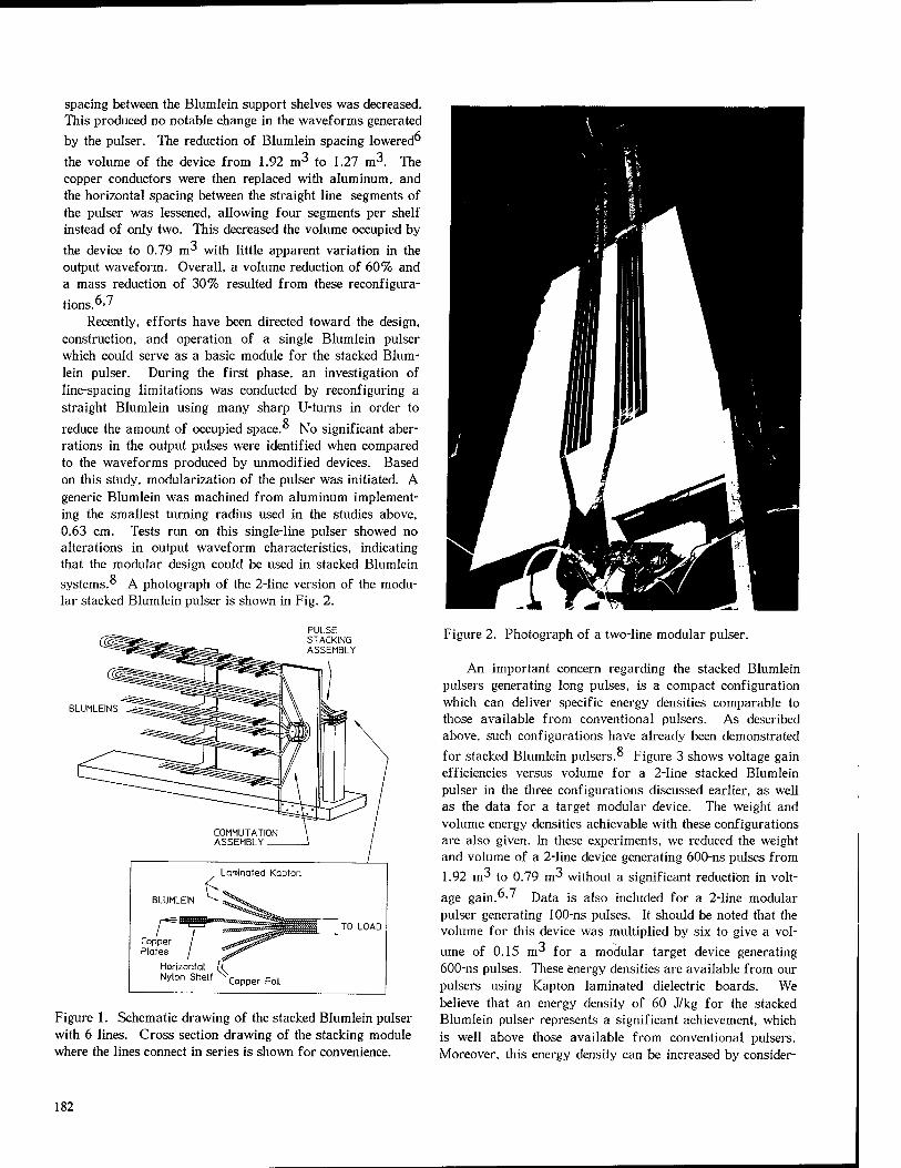
spacing between the Blumlein support shelves was decreased. This produced no notable change in the waveforms generated
by the pulser. The reduction of Blumlein spacing lowered"
the volume of the device from 1.92 m^ to 1.27 m^. The copper conductors were then replaced with aluminum, and the horizontal spacing between the straight line segments of the pulser was lessened, allowing four segments per shelf instead of only two. This decreased the volume occupied by
the device to 0.79 m^ with little apparent variation in the output waveform. Overall, a volume reduction of 60% and a mass reduction of 30% resulted from these reconfigura-
tions.6-7
Recently, efforts have been directed toward the design, construction, and operation of a single Blumlein pulser which could serve as a basic module for the stacked Blum- lein pulser. During the first phase, an investigation of line-spacing limitations was conducted by reconfiguring a straight Blumlein using many sharp U-turns in order to
reduce the amount of occupied space. No significant aber- rations in the output pulses were identified when compared to the waveforms produced by unmodified devices. Based on this study, modularization of the pulser was initiated. A generic Blumlein was machined from aluminum implement- ing the smallest turning radius used in the studies above, 0.63 cm. Tests run on this single-line pulser showed no alterations in output waveform characteristics, indicating that the modular design could be used in stacked Blumlein
systems." A photograph of the 2-line version of the modu- lar stacked Blumlein pulser is shown in Fig. 2.
BLUMLEINS
TO LOAD
Horizontal AT Nylon Shelf ^>Copper Foi[
Figure 1. Schematic drawing of the stacked Blumlein pulser with 6 lines. Cross section drawing of the stacking module where the lines connect in series is shown for convenience.
Figure 2. Photograph of a two-line modular pulser.
An important concern regarding the stacked Blumlein pulsers generating long pulses, is a compact configuration which can deliver specific energy densities comparable to those available from conventional pulsers. As described above, such configurations have already been demonstrated
for stacked Blumlein pulsers." Figure 3 shows voltage gain efficiencies versus volume for a 2-line stacked Blumlein pulser in the three configurations discussed earlier, as well as the data for a target modular device. The weight and volume energy densities achievable with these configurations are also given. In these experiments, we reduced the weight and volume of a 2-line device generating 600-ns pulses from
1.92 m^ to 0.79 m^ without a significant reduction in volt-
age gain."'' Data is also included for a 2-line modular pulser generating 100-ns pulses. It should be noted that the volume for this device was multiplied by six to give a vol-
ume of 0.15 m-^ for a modular target device generating 600-ns pulses. These energy densities are available from our pulsers using Kapton laminated dielectric boards. We believe that an energy density of 60 J/kg for the stacked Blumlein pulser represents a significant achievement, which is well above those available from conventional pulsers. Moreover, this energy density can be increased by consider-
182
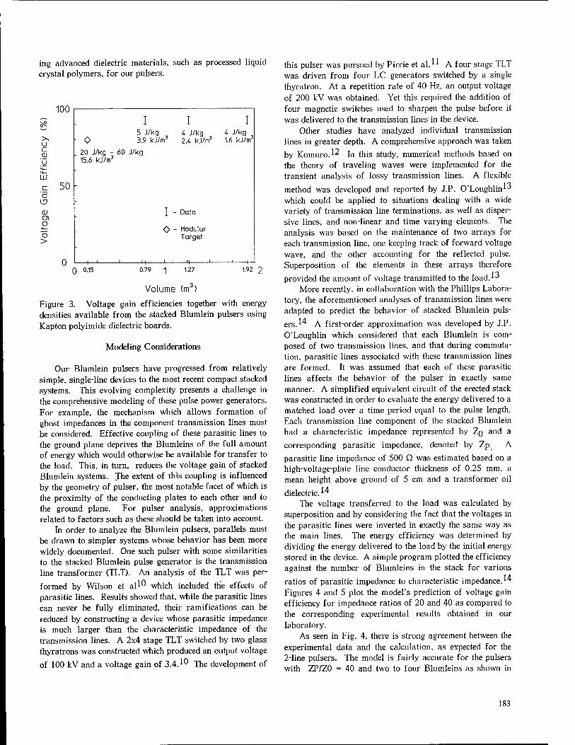
ing advanced dielectric materials, such as processed liquid crystal polymers, for our pulsers.
100
u c QJ
'u M—
ijj c 'a ID
ai en a
"o >
50 -
I I I 5 J/kg
■ O 3.9 kJ/m3 4 J/kg 2.4 kJ/nT
4 J/kg 1.6 kJ/m3
20 J/kg - 60 J/kg 15.6 kJ/m3
I - - Data
o- - Modular Target
,_. 1 H L_ H 1— ' 1—
0 °-15 0.79 1 1.27 1.92 2
Volume (m3)
Figure 3. Voltage gain efficiencies together with energy densities available from the stacked Blumlein pulsers using Kapton polyimide dielectric boards.
Modeling Considerations
Our Blumlein pulsers have progressed from relatively simple, single-line devices to the most recent compact stacked systems. This evolving complexity presents a challenge in the comprehensive modeling of these pulse power generators. For example, the mechanism which allows formation of ghost impedances in the component transmission lines must be considered. Effective coupling of these parasitic lines to the ground plane deprives the Blumleins of the full amount of energy which would otherwise be available for transfer to the load. This, in turn, reduces the voltage gain of stacked Blumlein systems. The extent of this coupling is influenced by the geometry of pulser, the most notable facet of which is the proximity of the conducting plates to each other and to the ground plane. For pulser analysis, approximations related to factors such as these should be taken into account.
In order to analyze the Blumlein pulsers, parallels must be drawn to simpler systems whose behavior has been more widely documented. One such pulser with some similarities to the stacked Blumlein pulse generator is the transmission line transformer (TLT). An analysis of the TLT was per-
formed by Wilson et al1" which included the effects of parasitic lines. Results showed that, while the parasitic lines can never be fully eliminated, their ramifications can be reduced by constructing a device whose parasitic impedance is much larger than the characteristic impedance of the transmission lines. A 2x4 stage TLT switched by two glass thyratrons was constructed which produced an output voltage
of 100 kV and a voltage gain of 3.4.1" -r^e development of
this pulser was pursued by Pirrie et al. A four stage TLT was driven from four LC generators switched by a single thyratron. At a repetition rate of 40 Hz, an output voltage of 200 kV was obtained. Yet this required the addition of four magnetic switches used to sharpen the pulse before it was delivered to the transmission lines in the device.
Other studies have analyzed individual transmission lines in greater depth. A comprehensive approach was taken
by Komuro.12 In this study, numerical methods based on the theory of traveling waves were implemented for the transient analysis of lossy transmission lines. A flexible
method was developed and reported by J.P. O'Loughlin13
which could be applied to situations dealing with a wide variety of transmission line terminations, as well as disper- sive lines, and non-linear and time varying elements. The analysis was based on the maintenance of two arrays for each transmission line, one keeping track of forward voltage wave, and the other accounting for the reflected pulse. Superposition of the elements in these arrays therefore
provided the amount of voltage transmitted to the load.13
More recently, in collaboration with the Phillips Labora- tory, the aforementioned analyses of transmission lines were adapted to predict the behavior of stacked Blumlein puls-
ers. 14 A first-order approximation was developed by J.P. O'Loughlin which considered that each Blumlein is com- posed of two transmission lines, and that during commuta- tion, parasitic lines associated with these transmission lines are formed. It was assumed that each of these parasitic lines affects the behavior of the pulser in exactly same manner. A simplified equivalent circuit of the erected stack was constructed in order to evaluate the energy delivered to a matched load over a time period equal to the pulse length. Each transmission line component of the stacked Blumlein had a characteristic impedance represented by ZQ and a
corresponding parasitic impedance, denoted by Zp A
parasitic line impedance of 500 Q was estimated based on a high-voltage-plate line conductor thickness of 0.25 mm, a mean height above ground of 5 cm and a transformer oil
dielectric. 1* The voltage transferred to the load was calculated by
superposition and by considering the fact that the voltages in the parasitic lines were inverted in exactly the same way as the main lines. The energy efficiency was determined by dividing the energy delivered to the load by the initial energy stored in the device. A simple program plotted the efficiency against the number of Blumleins in the stack for various
ratios of parasitic impedance to characteristic impedance.14
Figures 4 and 5 plot the model's prediction of voltage gain efficiency for impedance ratios of 20 and 40 as compared to the corresponding experimental results obtained in our laboratory.
As seen in Fig. 4, there is strong agreement between the experimental data and the calculation, as expected for the 2-line pulsers. The model is fairly accurate for the pulsers with ZP/Z0 = 40 and two to four Blumleins as shown in
183
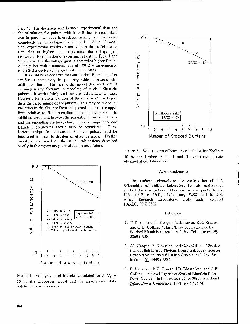
Fig. 4. The deviation seen between experimental data and the calculation for pulsers with 6 or 8 lines is most likely due to parasitic mode interactions arising from increased complexity in the configuration of the Blumleins. In addi- tion, experimental results do not support the model predic- tion that at higher load impedances the voltage gain decreases. Examination of experimental data in Figs. 4 and 5 indicates that the voltage gain is somewhat higher for the 2-line pulser with a matched load of 100 Q when compared to the 2-line device with a matched load of 50 Q.
It should be emphasized that our stacked Blumlein pulser exhibits a complexity in geometry which increases with additional lines. The first order model described here is certainly a step forward in modeling of stacked Blumlein pulsers. It works fairly well for a small number of lines. However, for a higher number of lines, the model underpre- dicts the performance of the pulsers. This may be due to the variation in the distance from the ground plane of the upper lines relative to the assumption made in the model. In addition, cross talk between the parasitic modes, switch type and corresponding risetime, charging source impedance and Blumlein geometries should also be considered. These factors, unique to the stacked Blumlein pulser, must be integrated in order to develop an effective model. Further investigations based on the initial calculations described briefly in this report are planned for the near future.
100
U c cy
LU
C 'a ID
QJ Dl
_D
~o >
10
Experimental
ZP/ZO - 20
o - 2-line B. 9.2 m
A - 2-line B. 17 m
»- 2-line B, 32.6 m
D - 2-line B. 48.2 m
+ - 2-line B. 48.2 m volume reduced o - 2-line B. photoconductively switched
123-456789 10
Number of Stacked Blumleins
Figure 4. Voltage gain efficiencies calculated for Zp/ZQ =
20 by the first-order model and the experimental data obtained at our laboratory.
100
u c gj "u
ÜJ
c D
ID
QJ Ol D
O >
10
ZP/ZO = 40
o - Experimental ZP/ZO - 40
123456789 10
Number of Stacked Blumleins
Figure 5. Voltage gain efficiencies calculated for Zp/Zg =
40 by the first-order model and the experimental data obtained at our laboratory.
Acknowledgments
The authors acknowledge the contribution of J.P. O'Loughlin of Phillips Laboratory for his analyses of stacked Blumlein pulsers. This work was supported by the U.S. Air Force Phillips Laboratory, WSQ, and the U.S. Army Research Laboratory, PSD under contract DAAL01-95-K-3502.
References
1. F. Davanloo, J.J. Coogan, T.S. Bowen, R.K. Krause, and C.B. Collins, "Flash X-ray Source Excited by Stacked Blumlein Generators," Rev. Sei. Instrum. 59, 2260 (1988).
2. J.J. Coogan, F. Davanloo, and C.B. Collins, "Produc- tion of High Energy Photons from Flash X-ray Sources Powered by Stacked Blumlein Generators," Rev. Sei. Instrum. 61, 1448 (1990).
3. F. Davanloo, R.K. Krause, J.D. Bhawalkar, and C.B. Collins, "A Novel Repetitive Stacked Blumlein Pulse Power Source," in Proceedings of the 8th International Pulsed Power Conference, 1991, pp. 971-974.
184
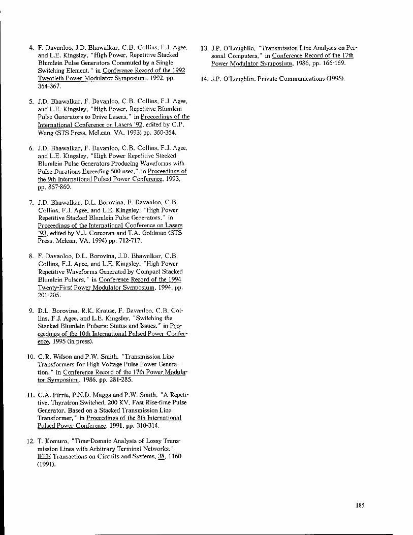
4. F. Davanloo, J.D. Bhawalkar, C.B. Collins, F.J. Agee, and L.E. Kingsley, "High Power, Repetitive Stacked Blumlein Pulse Generators Commuted by a Single Switching Element," in Conference Record of the 1992 Twentieth Power Modulator Symposium, 1992, pp. 364-367.
13. J.P. O'Loughlin, "Transmission Line Analysis on Per- sonal Computers," in Conference Record of the 17th Power Modulator Symposium, 1986, pp. 166-169.
14. J.P. O'Loughlin, Private Communications (1995).
5. J.D. Bhawalkar, F. Davanloo, C.B. Collins, F.J. Agee, and L.E. Kingsley, "High Power, Repetitive Blumlein Pulse Generators to Drive Lasers," in Proceedings of the International Conference on Lasers '92, edited by C.P. Wang (STS Press, McLean, VA, 1993) pp. 360-364.
6. J.D. Bhawalkar, F. Davanloo, C.B. Collins, F.J. Agee, and L.E. Kingsley, "High Power Repetitive Stacked Blumlein Pulse Generators Producing Waveforms with Pulse Durations Exceeding 500 nsec," in Proceedings of the 9th International Pulsed Power Conference, 1993, pp. 857-860.
7. J.D. Bhawalkar, D.L. Borovina, F. Davanloo, C.B. Collins, F.J. Agee, and L.E. Kingsley, "High Power Repetitive Stacked Blumlein Pulse Generators," in Proceedings of the International Conference on Lasers '93, edited by V.J. Corcoran and T.A. Goldman (STS Press, Mclean, VA, 1994) pp. 712-717.
8. F. Davanloo, D.L. Borovina, J.D. Bhawalkar, C.B. Collins, F.J. Agee, and L.E. Kingsley, "High Power Repetitive Waveforms Generated by Compact Stacked Blumlein Pulsers," in Conference Record of the 1994 Twenty-First Power Modulator Symposium, 201-205.
1994, pp.
9. D.L. Borovina, R.K. Krause, F. Davanloo, C.B. Col- lins, F.J. Agee, and L.E. Kingsley, "Switching the Stacked Blumlein Pulsers: Status and Issues," in Pro- ceedings of the 10th International Pulsed Power Confer- ence, 1995 (in press).
10. C.R. Wilson and P.W. Smith, "Transmission Line Transformers for High Voltage Pulse Power Genera- tion, " in Conference Record of the 17th Power Modula- tor Symposium, 1986, pp. 281-285.
11. C.A. Pirrie, P.N.D. Maggs and P.W. Smith, "A Repeti- tive, Thyratron Switched, 200 KV, Fast Rise-time Pulse Generator, Based on a Stacked Transmission Line Transformer," in Proceedings of the 8th International Pulsed Power Conference, 1991, pp. 310-314.
12. T. Komuro, "Time-Domain Analysis of Lossy Trans- mission Lines with Arbitrary Terminal Networks," IEEE Transactions on Circuits and Systems, 38, 1160 (1991).
185
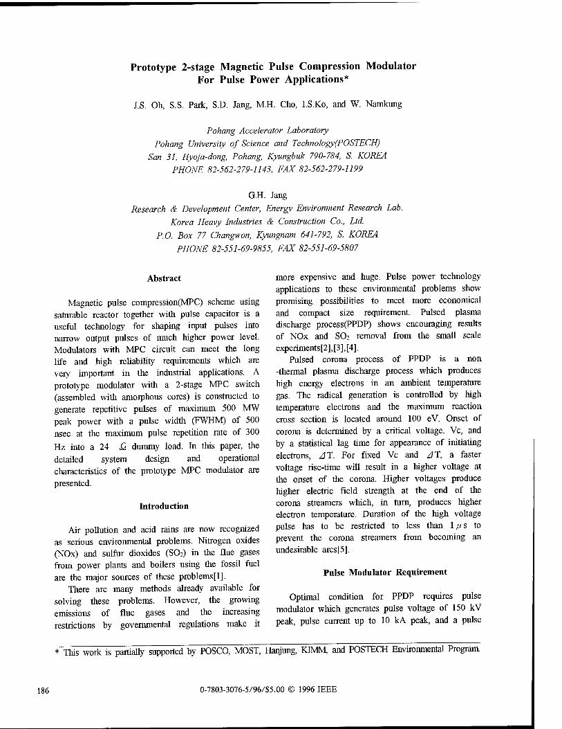
Prototype 2-stage Magnetic Pulse Compression Modulator For Pulse Power Applications*
J.S. Oh, S.S. Park, S.D. Jang, M.H. Cho, I.S.Ko, and W. Namkung
Pohang Accelerator Laboratory
Pohang University of Science and Technology(POSTECH)
San 31, Hyoja-dong, Pohang, Kyungbuk 790-784, S. KOREA
PHONE 82-562-279-1143, FAX 82-562-279-1199
G.H. Jang
Research & Development Center, Energy Environment Research Lab.
Korea Heavy Industries & Construction Co., Ltd.
P.O. Box 77 Changwon, Kyungnam 641-792, S. KOREA
PHONE 82-551-69-9855, FAX 82-551-69-5807
Abstract
Magnetic pulse compression(MPC) scheme using saturable reactor together with pulse capacitor is a useful technology for shaping input pulses into narrow output pulses of much higher power level. Modulators with MPC circuit can meet the long life and high reliability requirements which are very important in the industrial applications. A prototype modulator with a 2-stage MPC switch (assembled with amorphous cores) is constructed to generate repetitive pulses of maximum 500 MW peak power with a pulse width (FWHM) of 500 nsec at the maximum pulse repetition rate of 300
Hz into a 24 Q. dummy load. In this paper, the detailed system design and operational characteristics of the prototype MPC modulator are presented.
Introduction
Air pollution and acid rains are now recognized as serious environmental problems. Nitrogen oxides (NOx) and sulfur dioxides (S02) in the flue gases from power plants and boilers using the fossil fuel are the major sources of these problems[l].
There are many methods already available for solving these problems. However, the growing emissions of flue gases and the increasing restrictions by governmental regulations make it
more expensive and huge. Pulse power technology applications to these environmental problems show promising possibilities to meet more economical and compact size requirement. Pulsed plasma discharge process(PPDP) shows encouraging results of NOx and SO2 removal from the small scale experiments[2],[3],[4].
Pulsed corona process of PPDP is a non -thermal plasma discharge process which produces high energy electrons in an ambient temperature gas. The radical generation is controlled by high temperature electrons and the maximum reaction cross section is located around 100 eV. Onset of corona is determined by a critical voltage, Vc, and by a statistical lag time for appearance of initiating electrons, zJT. For fixed Vc and JT, a faster voltage rise-time will result in a higher voltage at the onset of the corona. Higher voltages produce higher electric field strength at the end of the corona streamers which, in turn, produces higher electron temperature. Duration of the high voltage pulse has to be restricted to less than 1 ß s to prevent the corona streamers from becoming an undesirable arcs[5].
Pulse Modulator Requirement
Optimal condition for PPDP requires pulse modulator which generates pulse voltage of 150 kV peak, pulse current up to 10 kA peak, and a pulse
* This work is partially supported by POSCO, MOST, Hanjung, KIMM, and POSTECH Environmental Program
186 0-7803-3076-5/96/S5.00 © 1996 IEEE
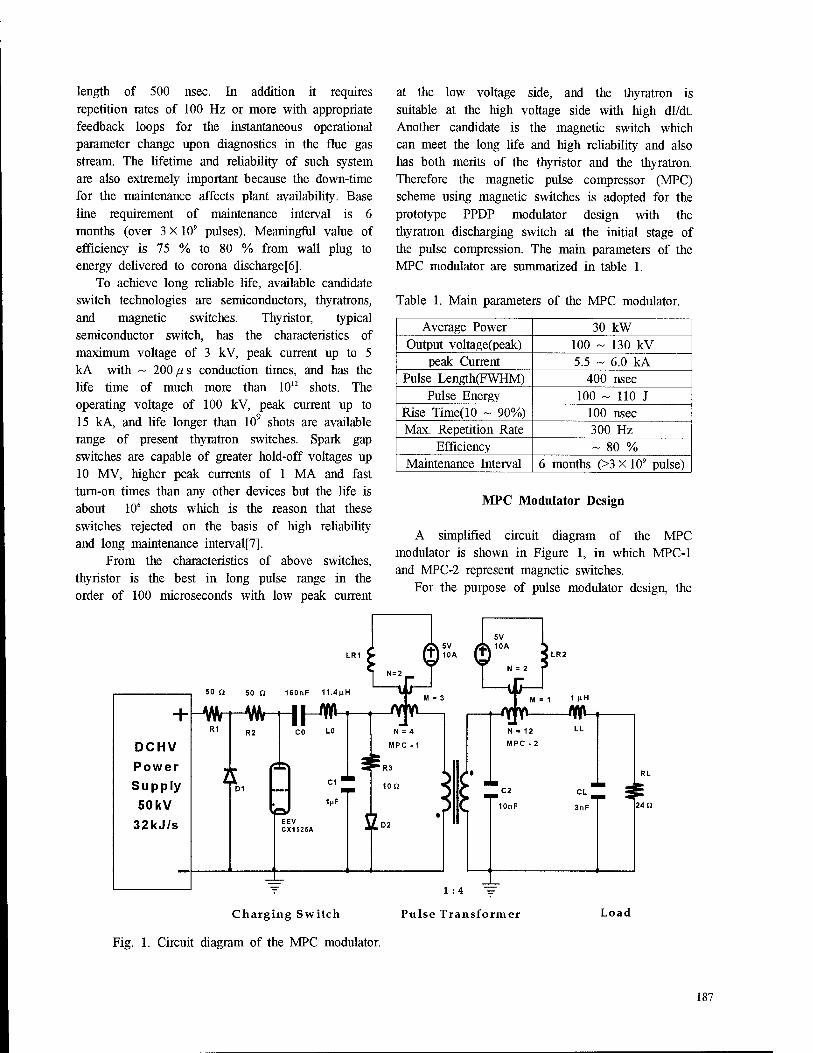
length of 500 nsec. In addition it requires repetition rates of 100 Hz or more with appropriate feedback loops for the instantaneous operational parameter change upon diagnostics in the flue gas stream. The lifetime and reliability of such system are also extremely important because the down-time for the maintenance affects plant availability. Base line requirement of maintenance interval is 6 months (over 3 X10⁹ pulses). Meaningful value of efficiency is 75 % to 80 % from wall plug to energy delivered to corona discharge [6].
To achieve long reliable life, available candidate switch technologies are semiconductors, thyratrons, and magnetic switches. Thyristor, typical semiconductor switch, has the characteristics of maximum voltage of 3 kV, peak current up to 5 kA with ~ 200/us conduction times, and has the life time of much more than 1012 shots. The operating voltage of 100 kV, peak current up to 15 kA, and life longer than 109 shots are available range of present thyratron switches. Spark gap switches are capable of greater hold-off voltages up 10 MV, higher peak currents of 1 MA and fast turn-on times than any other devices but the life is about 106 shots which is the reason that these switches rejected on the basis of high reliability and long maintenance interval[7].
From the characteristics of above switches, thyristor is the best in long pulse range in the order of 100 microseconds with low peak current
at the low voltage side, and the thyratron is suitable at the high voltage side with high dl/dt. Another candidate is the magnetic switch which can meet the long life and high reliability and also has both merits of the thyristor and the thyratron. Therefore the magnetic pulse compressor (MPC) scheme using magnetic switches is adopted for the prototype PPDP modulator design with the thyratron discharging switch at the initial stage of the pulse compression. The main parameters of the MPC modulator are summarized in table 1.
Table 1. Main parameters of the MPC modulator.
Average Power 30 kW Output voltage(peak) 100 ~ 130 kV
peak Current 5.5 ~ 6.0 kA Pulse Length(FWHM) 400 nsec
Pulse Energy 100 ~ 110 J Rise Time(10 ~ 90%) 100 nsec Max. Repetition Rate 300 Hz
Efficiency ~ 80 % Maintenance Interval 6 months (>3 X 10' pulse)
MPC Modulator Design
A simplified circuit diagram of the MPC modulator is shown in Figure 1, in which MPC-1 and MPC-2 represent magnetic switches.
For the purpose of pulse modulator design, the
Charging Switch
Fig. 1. Circuit diagram of the MPC modulator.
1:4 "^
Pulse Transformer Load
187
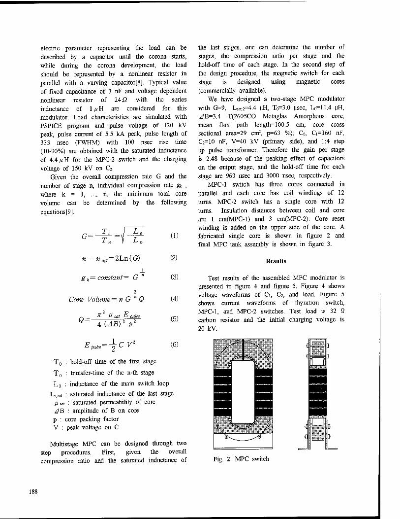
electric parameter representing the load can be described by a capacitor until the corona starts, while during the corona development, the load should be represented by a nonlinear resistor in parallel with a varying capacitor[8]. Typical value of fixed capacitance of 3 nF and voltage dependent nonlinear resistor of 24 Q with the series inductance of 1/^H are considered for this modulator. Load characteristics are simulated with PSPICE program and pulse voltage of 120 kV peak, pulse current of 5.5 kA peak, pulse length of 333 nsec (FWHM) with 100 nsec rise time (10-90%) are obtained with the saturated inductance of 4.4 ^H for the MPC-2 switch and the charging voltage of 150 kV on C2.
Given the overall compression rate G and the number of stage n, individual compression rate gk , where k = 1, ..., n, the minimum total core volume can be determined by the following equations [9].
Tf. T -*■ *
L, L
n- = noPt=2Ln(G)
g k= constant = G
_2
Core Volume= n G " Q
K ß sat ^ pulse Q-- 4 {AB)1 p'
E puke' \cv*
(1)
(2)
(3)
(4)
(5)
(6)
To Tn
L0
-Lr^sat
ß sat
AB
hold-off time of the first stage
transfer-time of the n-th stage
inductance of the main switch loop
saturated inductance of the last stage saturated permeability of core amplitude of B on core
p : core packing factor V : peak voltage on C
Multistage MPC can be designed through two step procedures. First, given the overall compression ratio and the saturated inductance of
the last stages, one can determine the number of stages, the compression ratio per stage and the hold-off time of each stage. In the second step of the design procedure, the magnetic switch for each stage is designed using magnetic cores (commercially available).
We have designed a two-stage MPC modulator with G=9, LSat,2=4.4 uH, T0=3.0 Lisec, Lo=11.4 |iH, JB=3.4 T(2605CO Metaglas Amorphous core, mean flux path length=100.5 cm, core cross sectional area=29 cm2, p=63 %), Co, G=160 nF, C2=10 nF, V=40 kV (primary side), and 1:4 step up pulse transformer. Therefore the gain per stage is 2.48 because of the peaking effect of capacitors on the output stage, and the hold-off time for each stage are 963 nsec and 3000 nsec, respectively.
MPC-1 switch has three cores connected in parallel and each core has coil windings of 12 turns. MPC-2 switch has a single core with 12 turns. Insulation distances between coil and core are 1 cm(MPC-l) and 3 cm(MPC-2). Core reset winding is added on the upper side of the core. A fabricated single core is shown in figure 2 and final MPC tank assembly is shown in figure 3.
Results
Test results of the assembled MPC modulator is presented in figure 4 and figure 5. Figure 4 shows voltage waveforms of G, Ci, and load. Figure 5 shows current waveforms of thyratron switch, MPC-1, and MPC-2 switches. Test load is 32 Q carbon resistor and the initial charging voltage is 20 kV.
i )
) Q
i
C
i i
>
> l*Ä*:?;:l
Fig. 2. MPC switch
188
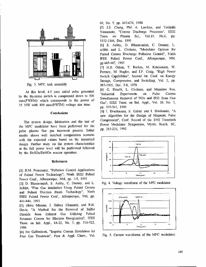
Fig. 3. MPC tank assembly
At this level, 4.5 |isec initial pulse generated by the thyratron switch is compressed down to 500 nsec(FWHM) which corresponds to the power of 35 MW with 100 nsec(FWTM) voltage rise time.
Conclusions
The system design, fabrication and the test of the MPC modulator have been performed for the pulse plasma flue gas treatment process. Initial results shows well matched compression scenario with the expected values based on the numerical design. Further study on the system characteristics at the full power level will be performed followed by the DeSOx/DeNOx reactor operation.
References
[1] B.M. Penetrante, "Pollution Control Applications of Pulsed Power Technology", Ninth IEEE Pulsed Power Conf, Albuquerque, NM, pp. 1-5, 1993 [2] D. Bhasavanish, S. Ashby, C. Deeney, and L. Schritt, "Flue Gas Irradiation Using Pulsed Corona and Pulsed Electron Beam Technology", Ninth IEEE Pulsed Power Conf., Albuquerque, NM, pp. 441-444, 1993 [3] Akira Mizuno, J. Sidney Clements, and R.H. Davis, "A Method for the Removal of Sulfur Dioxide from Exhaust Gas Utilizing Pulsed Streamer Corona for Electron Energization", IEEE Trans, on Ind. Appl., IA-22, No. 3, pp. 516-522, 1986 [4] Ivo Gallimberti, "Impulse Corona Simulation for Flue Gas Treatment", Pure & Appl. Chem., Vol.
60, No. 5, pp. 663-674, 1988 [5] J.S. Chang, Phil A. Lawless, and Toshiaki Yamamoto, "Corona Discharge Processes", IEEE Trans, on Plasma Sei., Vol.19, No.6, pp. 1152-1166, Dec. 1991 [6] S. Ashby, D. Bhasavanish, C. Deeney, L. schlitt and L. Civitano, "Modulator Options for Pulsed Corona Discharge Pollution Control", Ninth IEEE Pulsed Power Conf., Albuquerque, NM, pp.445-447, 1993 [7] H.B. Odom, T. Burkes, M. Kristiansen, W. Portnoy, M. Hagler, and J.P. Craig, "High Power Switch Capabilities", Second Int. Conf. on Energy Storage, Compression, and Switching, Vol. 2, pp. 987-1005, Dec. 5-8, 1978 [8] G. Dinelli, L. Civitano, and Massimo Rea, "Industrial Experiments on Pulse Corona Simultaneous Removal of NOx and S02 from Flue Gas", IEEE Trans, on Ind. Appl., Vol. 26, No. 3, pp. 535-541, 1990 [9] I. Druckmann, S. Gabay and I. Similanski, "A new Algorithm for the Design of Magnetic Pulse Compressors", Conf. Record of the 1992 Twentieth Power Modulator Symposium, Myrtle Beach, SC, pp. 213-216, 1992
B0
60
5 40
I 0 20 >
0
-2 0
V(C-2)
V(C-l) / A V(Lo«d)
5 10 Time(|isec)
15 20
Fig. 4. Voltage waveforms of the MPC modulator.
I(Thyrairon) I(M PC-2)
iJ Vl(MPC-l)
Fig. 5. Current waveforms of the MPC modulator.
189
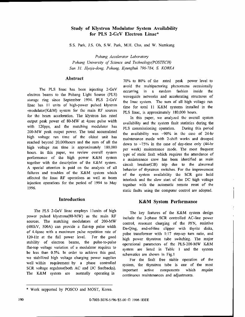
Study of Klystron Modulator System Availability for PLS 2-GeV Electron Linac*
S.S. Park, J.S. Oh, S.W. Park, M.H. Cho, and W. Namkung
Pohang Accelerator Laboratory
Pohang University of Science and Technology (POSTECH)
San 31, Hyoja-dong, Pohang, Kyungbuk 790-784, S. KOREA
Abstract
The PLS linac has been injecting 2-GeV electron beams to the Pohang Light Source (PLS) storage ring since September 1994. PLS 2-GeV linac has 11 units of high-power pulsed klystron -modulator(K&M) system for the main RF sources for the beam acceleration. The klystron has rated output peak power of 80-MW at 4|isec pulse width with 120pps, and the matching modulator has 200-MW peak output power. The total accumulated high voltage run time of the oldest unit has reached beyond 20,000hours and the sum of all the high voltage run time is approximately 180,000 hours. In this paper, we review overall system performance of the high power K&M system together with the description of the K&M system. A special attention is paid on the analysis of all failures and troubles of the K&M system which affected the linac RF operations as well as beam injection operations for the period of 1994 to May 1996.
Introduction
The PLS 2-GeV linac employs llunits of high power pulsed klystrons(80-MW) as the main RF sources. The matching modulators of 200-MW (400kV, 500A) can provide a flat-top pulse width of 4.4|tsec with a maximum pulse repetition rate of 120-Hz at the full power level. For the good stability of electron beams, the pulse-to-pulse flat-top voltage variation of a modulator requires to be less than 0.5%. In order to achieve this goal, we stabilized high voltage charging power supplies well within requirement by a phase controlled SCR voltage regulator(both AC and DC feedbacks). The K&M system are normally operating in
70% to 80% of the rated peak power level to avoid the multipactoring phenomena occasionally occurring in a random fashion inside the waveguide networks and accelerating structures of the linac system. The sum of all high voltage run time for total 11 K&M systems installed in the PLS linac, is approximately 180,000 hours.
In this paper, we analyzed the overall system availability and the system fault statistics during the PLS commissioning operation. During this period the availability was -90% in the case of 24-hr maintenance mode with 2-shift works and drooped down to -75% in the case of day-time only (44-hr per week) maintenance mode. The most frequent type of static fault which requires the attendance of a maintenance crew has been identified as main circuit breaker(CB) trip due to the abnormal behavior of thyratron switches. For the improvement of the system availability the SCR gate hold interlock and the slow start of the DC high voltage together with the automatic remote reset of the
static faults using the computer control are adopted.
K&M System Performance
The key features of the K&M system design include the 3-phase SCR controlled AC-line power control, resonant charging of the PFN, resistive De-Qing, end-of-line clipper with thyrite disks, pulse transformer with 1:17 step-up turn ratio, and high power thyratron tube switching. The major operational parameters of the PLS-200-MW K&M system are listed in Table 1 and the system schematics are shown in Fig.l
For the fault free stable operation of the system, the thyratron tube is one of the most important active components which require continuous maintenances and adjustments.
* Work supported by POSCO and MOST, Korea.
190 0-7803-3076-5/96/S5.00 © 1996 IEEE
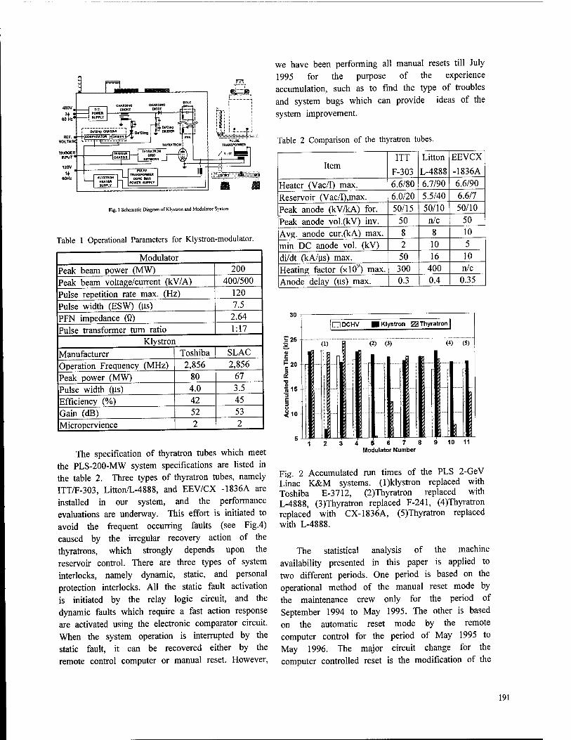
Fig. 1 Schematic Diagram of Klystron and Modulator System
Table 1 Operational Parameters for Klystron -modulator.
Modulator Peak beam power (MW) 200
Peak beam voltage/current (kV/A) 400/500
Pulse repetition rate max. (Hz) 120
Pulse width (ESW) (us) 7.5
PFN impedance (fi) 2.64
Pulse transformer turn ratio 1:17 Klystron
Manufacturer Toshiba SLAC
Operation Frequency (MHz) 2,856 2,856
Peak power (MW) 80 67
Pulse width ((is) 4.0 3.5
Efficiency (%) 42 45
Gain (dB) 52 53
Micropervience 2 2
The specification of thyratron tubes which meet the PLS-200-MW system specifications are listed in the table 2. Three types of thyratron tubes, namely ITT/F-303, Litton/L-4888, and EEV/CX -1836A are installed in our system, and the performance evaluations are underway. This effort is initiated to avoid the frequent occurring faults (see Fig.4) caused by the irregular recovery action of the thyratrons, which strongly depends upon the reservoir control. There are three types of system interlocks, namely dynamic, static, and personal protection interlocks. All the static fault activation is initiated by the relay logic circuit, and the dynamic faults which require a fast action response are activated using the electronic comparator circuit. When the system operation is interrupted by the static fault, it can be recovered either by the remote control computer or manual reset. However,
we have been performing all manual resets till July 1995 for the purpose of the experience accumulation, such as to find the type of troubles and system bugs which can provide ideas of the system improvement.
Table 2 Comparison of the thyratron tubes.
Item ITT
F-303
Litton
L-4888
EEVCX
-1836A
Heater (Vac/I) max. 6.6/80 6.7/90 6.6/90
Reservoir (Vac/I),max. 6.0/20 5.5/40 6.6/7
Peak anode (kV/kA) for. 50/15 50/10 50/10
Peak anode vol.(kV) inv. 50 n/c 50
Avg. anode cur.(kA) max. 8 8 10
min DC anode vol. (kV) 2 10 5
di/dt (kA/|is) max. 50 16 10
Heating factor (xl0y) max. 300 400 n/c
Anode delay (us) max. 0.3 0.4 0.35
30 ICZIDCHV M Klystron M Thyratron |
4 5 6 7 8 Modulator Number
Fig. 2 Accumulated run times of the PLS 2-GeV Linac K&M systems, (l)klysrron replaced with Toshiba E-3712, (2)Thyratron replaced with L-4888, (3)Thyratron replaced F-241, (4)Thyratron replaced with CX-1836A, (5)Thyratron replaced with L-4888.
The statistical analysis of the machine availability presented in this paper is applied to two different periods. One period is based on the operational method of the manual reset mode by the maintenance crew only for the period of September 1994 to May 1995. The other is based on the automatic reset mode by the remote computer control for the period of May 1995 to May 1996. The major circuit change for the computer controlled reset is the modification of the
191

CB trip interlock to activate SCR gate hold and the soft start of the DC high voltage.
System Availability Statistics
Since the completion of the PLS 2-GeV linac installation in December 1993, all the K&M systems have been in operation continuously except scheduled short-term shut downs. Fig. 2 shows the total accumulated times of klystron and thyratron heater operation, and the high voltage run. The sum of the high voltage run time of each modulator has reached over 180,000 hours, and the experience accumulated so far provides the valuable infor -mation for the systems stable operation.
Fig. 3 shows the monthly failure and down time statistics for the period of September 1994 to May 1995 (manual reset) and the period of May 1995 to May 1996 (auto reset).
50 [ Manual Reset Mode ) j f Automatic Reset Mode ]
16
14
9 11 1 3 1995
5 7 9 11 1 3 Month 1996
Fig. 3 Monthly failure and down time statistics of klystron-modulator system.
Machine availability analysis has been performed based on the data using the techniques described in detail in reference [3]. Fig.4 is the monthly availability and MTBF(mean time between failure) statistics of klystron-modulator system. The table 3 is the summary of the average fault analysis data. The MTBF calculated by dividing the sum of the accumulated modulator run time with the total fault count(MTBF=N*TO/FC). The MTTR (mean time to repair is equal to the total down time divided by total fault counts, MTTR=TD/FC).
120
110
100
[ 90
j 80
! 70
60
50
40
f Manual Reset Mode ] | [ Automatic Reset Mode ]
■m—
■
Availability
MTBF
—PT"*""-
■ ■
■
— W
■ N ■
- m ■
1 |. . ll.ll IIUBMHIII
10 > o
8 uT CO I-
6 2
9 111 3579 11 1 35 1995 Month 1996
Fig. 4 Monthly availability and MTBF statistics of klystron-modulator.
One can see in the table 3, approximately 76% of the machine availability (A=l-MTTR*FC/TO) has been improved to approximately 96% by applying auto reset mode operation with the simple CB trip modification, which is also shown in th'e Fig 3 & 4. It indicates most of the system troubles are not so serious, and in many cases they are easily recoverable.
Table 3 Fault analysis of klystron-modulator system for
PLS.
Item 94.9-95.5 95.5-96.5
Number of modulators, N 11 11 Spare no. of modulators 0 0 Operation time (hr)*1 , TO 6000 7560 Total failure counts, FC 226 115 Total down time (hr) 1468 344 MTBF(hr) 26.5 65.7 MTTR(hr/failure count) 6.5 2.988 System availability, A 0.76 0.96
1) Operation time for the statistical analysis.
Fig. 5 shows the total systems static fault count data collected during the period of September 1994 to May 1995. Fig. 6 is the total system static fault count data collected for the period of Jun 1995 to May 1996. From fig. 5 & 6 one can see the significant decrease in CB trip count by the CB trip modification and the apparent increase in klystron troubles as the accumulated run time increases.
192
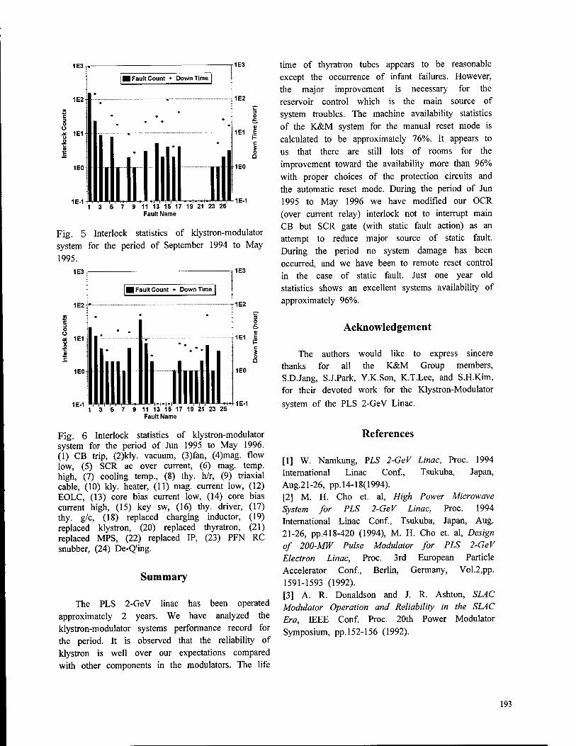
1E3
1E2
o ü
1E1
1E0
1E-1
I Fault Count • Down Time |
I 3 5 7
,|.|.|.|.l"l"i
1E3
1E2
1E1
o Q
9 11 13 15 17 19 21 23 25 Fault Name
1E0
1E-1
Fig. 5 Interlock statistics of klystron-modulator system for the period of September 1994 to May
1995. 1E3
1E2
u
8 1E1
1E<H
1E-1
| Fault Count • Down Time
1E3
1E2
1E1
i &
13 5 7 9 11 13 15 17 19 21 23 25 Fault Name
1E0
1E-1
Fig. 6 Interlock statistics of klystron-modulator system for the period of Jun 1995 to May 1996. (1) CB trip, (2)kly. vacuum, (3)fan, (4)mag. flow low, (5) SCR ac over current, (6) mag. temp, high, (7) cooling temp., (8) thy. h/r, (9) triaxial cable, (10) kly. heater, (11) mag. current low, (12) EOLC, (13) core bias current low, (14) core bias current high, (15) key sw, (16) thy. driver, (17) thy. g/c, (18) replaced charging inductor, (19) replaced klystron, (20) replaced thyratron, (21) replaced MPS, (22) replaced IP, (23) PFN RC snubber, (24) De-Q'ing.
Summary
The PLS 2-GeV linac has been operated approximately 2 years. We have analyzed the klystron-modulator systems performance record for the period. It is observed that the reliability of klystron is well over our expectations compared with other components in the modulators. The life
time of thyratron tubes appears to be reasonable except the occurrence of infant failures. However, the major improvement is necessary for the reservoir control which is the main source of system troubles. The machine availability statistics of the K&M system for the manual reset mode is calculated to be approximately 76%. It appears to us that there are still lots of rooms for the improvement toward the availability more than 96% with proper choices of the protection circuits and the automatic reset mode. During the period of Jun 1995 to May 1996 we have modified our OCR (over current relay) interlock not to interrupt main CB but SCR gate (with static fault action) as an attempt to reduce major source of static fault. During the period no system damage has been occurred, and we have been to remote reset control in the case of static fault. Just one year old statistics shows an excellent systems availability of approximately 96%.
Acknowledgement
The authors would like to express sincere thanks for all the K&M Group members, S.D.Jang, S.J.Park, Y.K.Son, K.T.Lee, and S.H.Kim, for their devoted work for the Klystron-Modulator
system of the PLS 2-GeV Linac.
References
[1] W. Namkung, PIS 2-GeV Linac, Proc. 1994 International Linac Conf., Tsukuba, Japan, Aug.21-26, pp. 14-18(1994). [2] M. H. Cho et. al, High Power Microwave System for PLS 2-GeV Linac, Proc. 1994 International Linac Conf, Tsukuba, Japan, Aug. 21-26, pp.418-420 (1994), M. H. Cho et. al, Design of 200-MW Pulse Modulator for PLS 2-GeV Electron Linac, Proc. 3rd European Particle Accelerator Conf., Berlin, Germany, Vol.2,pp. 1591-1593 (1992). [3] A. R. Donaldson and J. R. Ashton, SLAC Modulator Operation and Reliability in the SLAC Era, IEEE Conf. Proc. 20th Power Modulator Symposium, pp. 152-156 (1992).
193
The Performance of a Simple PFN Marx Generator
S J MacGregor, S M Turnbull, F A Tuema and J Harrower
Dept of Electronic and Electrical Engineering, University ofStrathclyde 204 George Street, Glasgow Gl 1XW, United Kingdom
Abstract
The performance of a 5-stage pulse forming network (PFN) Marx generator is described. Each stage of the generator was constructed from HV co-axial cable instead of discrete inductors and HV capacitors. The output voltage pulse from the generator is rectangular in profile, with a risetime of ~30ns and a duration of -100ns. The maximum output voltage is 200kV and the output impedance is 125Q. Due to the relatively small amount of energy stored in the device (~10J), it may be operated at pulse repetition frequencies of -100Hz.
Introduction
Conventional high voltage Marx generators are usually physically large devices and therefore have a significant level of self inductance. When this inductance is combined with the inductance of the output feed, the resulting risetime of the output pulse can be relatively slow (>50ns) unless peaking circuits are employed. The conventional Marx design produces an output pulse profile which is double exponential in nature. This makes it difficult to match the generator output pulse to a particular load, which in turn makes it difficult to transfer all of the energy stored in the generator to the load during one pulse.
In order to address the problems of matching, energy transfer efficiency and risetime, some Marx generators have been constructed using PFNs. Each stage of this type of Marx generator is comprised of a lumped element PFN instead of a discrete HV capacitor. The output pulse profile from a PFN Marx generator is rectangular and the output impedance is well defined. This enables accurate matching of the source and load which can result in high energy transfer efficiency to the load. However, the use of lumped element PFNs usually results in a large device due to the number of components used to construct the generator. This can also lead to problems of reliability and high construction and maintenance costs.
The PFN Marx generator described in this paper was
constructed using commercially available HV co-axial cable as the PFN elements rather than lumped element transmission lines. The versatility and availability of co-axial cable means that PFN Marx generators constructed in this way are straightforward to assemble, relatively compact and comparatively inexpensive. They are suitable for low to moderate energy applications (10-100J), including x-ray and (i- wave source power supplies, trigger generators and general HV load testing. The pulse repetition frequency at which they can operate is dependent upon the voltage recovery time of the stage switches, and the limits of the primary power supply.
Experimental
The particular PFN Marx generator evaluated here is comprised of 5 PFN stages although this can be altered to suit specific requirements. Each stage is constructed from a single length of co-axial cable which is wound in a dual pulse forming line arrangement. This minimises losses caused by open circuit end effects and also halves the impedance of each stage to 25£2, this being half the characteristic impedance of the co-axial cable. As there are five stages in the PFN Marx generator, the total output impedance is 125£X
There is 25m of co-axial cable used in each stage, 12.5m per pulse forming line, and these are wound as shown in Fig 1. The co-axial cable is clamped between two acrylic disc spacers which are 500mm in diameter, and the cable ends are located at the centre point for electrical connection to the spark gap column. Each stage of the generator is 40mm high and the stage spacing was set to 40mm.
The five stages of the generator are mounted on nylon screwed rod with the switch enclosure, which houses the five spark gaps, mounted in the centre, as shown in Fig 2. The design of the switch enclosure (or spark gap column) is such that the individual spark gaps within the column irradiate subsequent spark gaps upon closing. This self-irradiation of the spark gaps
194 0-7803-3076-5/96/55.00 © 1996 IEEE
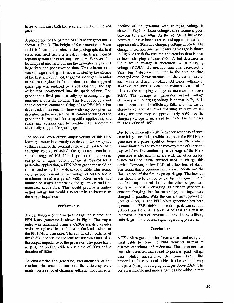
helps to minimise both the generator erection time and jitter.
A photograph of the assembled PFN Marx generator is shown in Fig 3. The height of the generator is 60cm and it is 50cm in diameter. In this photograph, the first stage was fired using a trigatron which was housed separately from the other stage switches. However, this technique of electrically firing the generator results in a large jitter and poor erection time. This is because the second stage spark gap is not irradiated by the closure of the first self contained, triggered spark gap. In order to reduce the jitter in the erection time, the triggered spark gap was replaced by a self closing spark gap which was incorporated into the spark column. The generator is fired pneumatically by releasing the gas pressure within the column. This technique does not enable precise command firing of the PFN Marx but does result in an erection time with very low jitter, as described in the next section. If command firing of the generator is required for a specific application, the spark gap column can be modified to incorporate electrically triggerable spark gaps.
The nominal open circuit output voltage of this PFN Marx generator is currently restricted to 200kV by the voltage rating of the co-axial cable which is 40kV. At a charging voltage of 40kV, the generator contains a stored energy of 10J. If a larger amount of stored energy or a higher output voltage is required for a particular application, a PFN Marx generator could be constructed using lOOkV dc co-axial cable. This would yield an open circuit output voltage of 500kV and a maximum stored energy of ~60J. Alternatively, the number of stages comprising the generator could be increased above five. This would provide a higher output voltage but would also result in an increase in the output impedance.
Performance
An oscillogram of the output voltage pulse from the PFN Marx generator is shown in Fig 4. The output pulse was measured using a CuS04 resistive divider which was placed in parallel with the load resistor of the PFN Marx generator. The combined impedance of the Q1SO4 divider and the load resistor was matched to the output impedance of the generator. The pulse has a rectangular profile, with a rise time of 30ns and a duration of 100ns.
To characterise the generator, measurements of the risetime, the erection time and the efficiency were made over a range of charging voltages. The change in
risetime of the generator with charging voltage is shown in Fig 5. At lower voltages, the risetime is poor, between 40ns and 60ns. As the voltage is increased, however, the risetime decreases and appears to settle at approximately 30ns at a charging voltage of 35kV. The change in erection time with charging voltage is shown in Fig 6. As with the risetime, the erection time is poor at lower charging voltages (>60ns), but decreases as the charging voltage is increased. At a charging voltage of 35kV, the erection time has decreased to 38ns. Fig 7 displays the jitter in the erection time averaged over 12 measurements of the erection time at each value of charging voltage. At lower voltages of 10-15kV, the jitter is ~3ns, and reduces to a level of ~lns as the charging voltage is increased to above 30kV. The change in generator output voltage efficiency with charging voltage is shown in Fig 8. It can be seen that the efficiency falls with increasing charging voltage. At lower charging voltages of 10- 20kV, the efficiency is approximately 90%. As the charging voltage is increased to 35kV, the efficiency falls to a value of-85%.
Due to the inherently high frequency response of most co-axial systems, it is possible to operate the PFN Marx generator at a pulse repetition frequency (PRF) which is only limited by the voltage recovery time of the spark gap switches. Conventionally, each stage of the Marx generator is charged in series with the other stages, which was the initial method used to charge this device. However, at low PRFs of a few tens of Hz, it was found that a common failure mechanism was the "locking on" of the first stage spark gap. The lock-on was thought to be caused by the fast charging time of the first stage, in relation to the other stages, that occurs with resistive charging. In order to generate a constant charging time for each stage, the stages were charged in parallel. With the current arrangement of parallel charging, the PFN Marx generator has been operated at a PRF 160Hz in a sealed spark gap column without gas flow. It is anticipated that this will be improved to PRFs of several hundred Hz by utilising suitable gas mixtures and higher operating pressures.
Conclusions
A PFN Marx generator has been constructed using co- axial cable to form the PFN elements instead of discrete capacitors and inductors. The generator has been characterised and found to possess good voltage gain whilst maintaining the transmission line properties of the co-axial cable. It also exhibits very low jitter (~lns) at charging voltages above 20kV. The design is flexible and more stages can be added, either
195
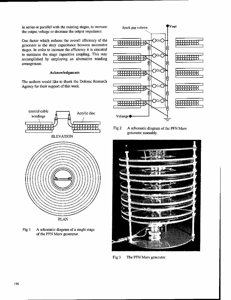
in series or parallel with the existing stages, to increase the output voltage or decrease the output impedance.
One factor which reduces the overall efficiency of the generator is the stray capacitance between successive stages. In order to increase the efficiency it is essential to minimise the stage capacitive coupling. This may accomplished by employing an alternative winding arrangement.
Acknowledgments
The authors would like to thank the Defense Research Agency for their support of this work.
Spark gap column
coaxial cable windings
Acrylic disc
ELEVATION
PLAN
Fig 1 A schematic diagram of a single stage of the PFN Marx generator.
Vout
\mmm
Vcharge#
Fig 2 A schematic diagram of the PFN Marx generator assembly.
Fig 3 The PFN Marx generator.
196
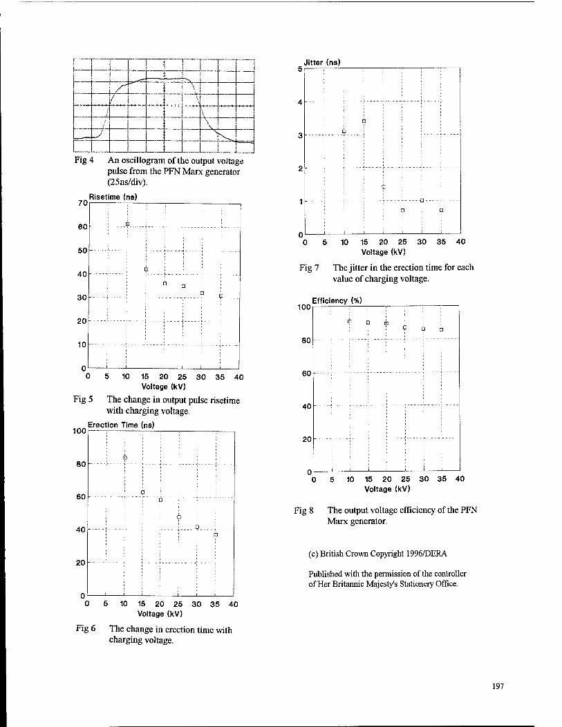
ÜX -n
/ \ \
Jitter (ns)
Fig 4 An oscillogram of the output voltage pulse from the PFN Marx generator (25ns/div).
Risetime (ns) 70
60
50
40
30
20
10
0 5 10 15 20 25 30 35 40 Voltage (kV)
Fig 5 The change in output pulse risetime with charging voltage.
Erection Time (ns) 100
80
60
_ m | :
° B _ | | | D $
40
20
[ ]
( 3
B ', I
p
B
□
' i i i i
0 5 10 15 20 25 30 35 40 Voltage (kV)
Fig 6 The change in erection time with charging voltage.
0 5 10 15 20 25 30 35 40 Voltage (kV)
Fig 7 The jitter in the erection time for each value of charging voltage.
100 Efficiency (%)
c 9 D B
1 i
80
60
40
20
0 5 10 15 20 25 30 35 40 Voltage (kV)
Fig 8 The output voltage efficiency of the PFN Marx generator.
(c) British Crown Copyright 1996/DERA
Published with the permission of the controller of Her Britannic Majesty's Stationery Office.
197
DEVELOPMENT OF ENHANCED FAULT-TOLERANCE FOR A 600 kV IMPULSE GENERATOR
by
J. L. Zirnheld*, V. G. Foley III, R. E. Dollinger and W. J. Sarjeant Bonner Hall - Room 312
High Power Electronics Institute State University of New York at Buffalo
P.O. Box 601900 - (716) 645-2422 ext 1216 Buffalo, NY 14260-1900
ABSTRACT
A Marx Bank is a voltage multiplication system, utilized for generation of high voltage impulses. The present system under study is a six stage Marx, of low impedance design for AC and DC transmission line surge testing. Six 100 kV, 0.5 pF capacitors (arranged in six stages) are charged in parallel, and discharged in series to produce a single shot "lightning-like" 5. to 1000. microsecond duration impulse waveform with peak voltage of 600 kV, along with 15 kJ of energy. Resistor elements in the Marx, used for charging and voltage equalization, were being destroyed when the 600 kV, Impulse Generator was discharged into a faulted load, particularly after a sequence of repetitive firings that ended in load breakdown. These front and tail pulse shaping resistors each consisted of four units in parallel Sometimes only one element of the four in parallel would "disappear," particularly if the Marx did not fully erect
A new type of a bulk ceramic tube resistor was developed through industrial participation, to eliminate resistor breakdown. There have been no further instances of resistor damage using the bulk ceramics. The methods and results of inductance determination of these units will be presented
Through a diagnostic sequence of experiments, it was determined that each OEM resistor consisted of two wire wound coils that were concentrically counter-wound, supposedly to attain a low inductance. In fact, the inductance varied from tens to hundreds of microhenries for the same resistance unit value. The volume of wire was quite small and Hie resultant energy inertia was insufficient for 15 kJ operation. The OEM said they would sell replacement sets of elements that would have an
inductance less than 1 pH, which was a specification of theirs, and 2.5 kJ energy absorption capability. Upon arrival, all were 10 pH,far to high to be of use. Therefore, HVR Advanced Power Components developed, for this application, a very low inductance high energy bulk ceramic tube resistor with a resistance rating of either 50. Ohms or 100. Ohms.
INTRODUCTION
High voltage generators are used in routine impulse or "surge" testing laboratories to confirm the efficiency and reliability of the insulation behavior under different conditions encountered by transformers, capacitors, cables, etc. High transient voltages can be produced by using several circuits of different sizes and shapes. The amplitude of the high voltage, is always related to the operating voltage while its shape is greatly influenced by the impedances and switching conditions of such circuits. Since a Marx Bank circuit can be used to generate high voltage, it may be used to simulate lightning strikes or switching surges [1]. Lightning strikes and switching surges can cause insulation breakdown. In order to perform reliable impulse testing it was necessary to have a robust, operational high voltage generator or Marx Bank.
During the firing of the Marx Bank into a short circuited load, too much energy was being put through the front and tail resistors. Calculations were performed consisting of various combinations of resistors while assuming two conditions, either the properly erected marxed case where all six stages are marxed, or a misfired case where one stage does not marx. The maximum amount of allowable energy through each individual element (or resistor) was determined [2]. For the Marx Bank located at the High
198 0-7803-3076-5/96/S5.00 © 1996 IEEE
Power Electronics Institute, it was determined that 50. Ohms and 100. Ohms resistors rated at 2.5 kJ with low inductance should be purchased. The energy of 2.5 kJ was chosen assuming worst case conditions. If the Marx Bank misfired into a short circuited load, energy across each front resistor was calculated to be 1.6 kJ. [2] With each resistor being rated at 2.5 kJ, this means that provided the bank is not fired more than once per minute or so the resistors should be able to handle a misfired condition. For the purpose of the study, low inductance is defined to be less than 1 .uH. Testing for the inductance of resistors is not trivial.
Table 3 is constructed from measurements taken using the test fixture shown in figure 1. It is a true coax configuration (where 4 is the zero inductance for coax) simulated by two wires on an outside path with the test sample as the return path. Since figure 1 is a schematic only, we note that the path consists of stripped 12 gauge wire. For ease of connection to the test sample, all connections are made with solder clip leads. Rather than crimp connections to the clip leds, they are soldered to get better low inductance connections.
Measurement Techniques
To measure the inductance, four separate techniques were determined to be appropriate because of the combination of a relatively large resistance (100. Ohm) with relatively low inductance (<3. microhenries). [4]
TABLE 1
Test Techniques
* Series Resonant * Capacitive Discharge * 100 kHz Bridge * 1,000 kHz Bridge
With the test techniques it is possible to use a capacitive discharge circuit. For our values of L's, C's and R's, it is necessary to look at the ringing and the over-damped cases [3]. Or one can use a digibridge at 100. kHz or 1,000. kHz, provided that the signal frequency is resonant.
TABLE 2
Figure 1. True Coax simulated by two wire down resistor (test sample) back
measure = Lloop +L««h(eW,erL^rLI)
Test Loads
* A 100. Ohm fixed carbon resistor in series with a 1. microhenries inductor
* A 100. Ohm fixed carbon resistor in series with a 10. microhenries inductor
* The 100. Ohm fixed carbon resistor only * A 1. microhenries inductor only * A 10. microhenries inductor only
In Table 3 is a representative sample of data collected. It should be noted that the 1. uH loop test was preformed twice, after manipulation of the fixture, sample and leads to show repeatability of results. With no test sample in the test fixture, the measured inductance value shown is the inductance of the clip leads and the two wire #12 gauge path [Figure 1]. Adding a tube of copper 1.25 cm in diameter and approximately 25. cm long to the test fixture shows no significant change in the inductance measured. This clearly shows the inductance shown is contained in the clip leads and #12 gauge return path. The test fixture itself [Figure 1] does not contribute significantly to the inductance of the sample being measured. The test
199
fixture should have a calculated inductance based on equation I [5].
-7 L =2x10 * In (D/a) * length, eq. I.
For the accuracies involved the theoretical value of the loop inductance is 4.6 x 10"7- The best ^^ can be said
for the accuracies involved in these measurements is that an inductance of 1. uH can easily be displayed. Therefore, one can assume that you could see 1/10 uH of inductance if it was there.
It should be noted that the OEM did provide one resistor of low inductance (i. e., less than one 1. uH). When counter wound correctly the resistors from the OEM are indeed of low inductance. Although, measurements were taken on all of the bulk ceramic resistors, only the worst case is presented. The HVR 100. ohm bulk ceramic element has an inductance of 1.26 uH. As shown from the earlier tests, most of the inductance comes from the test fixture. Therefore, for the accuracies involved the actual inductance of the HVR resistor can only be approximated to be less than 0.5 microhenries.
TABLE 3
Measurements taken from RLC digibridge frequency = 100. kHz
Description
1. uH loop 1. uH loop test fixture (no sample) copper tube 1.25 cm diameter 25 cm long bulk ceramic resistor 2 W, 100. Ohms carbon resistor Carbon resistor in series w/1 uH loop OEM 150 Ohm OEM 75 Ohm OEM 1,000. Ohm HVR 100 Ohm
LfuH) R fOhms)
1.69 18. 60. 1.64 18. 60. 0.85 11. 46. 0.88 11. 50. 0.85 0.006 97.05 0.72 0.004 103.18 1.71 0.01 103.22 2.64 0.01 152.19 2.41 0.02 75.56 0.9 0.0006 1,009.7 1.26 0.0076 97.05
Depending on the frequency of the measurements taken, the inductance will vary from test sample to test sample. This has to do with the skin effect [6]. Skin effect is a result of the magnetic flux lines that circle part but not all of the conductor. At high frequencies, the current in a conductor is not uniformly distributed over the cross sectional area of the conductor but tends to be concentrated near the surface. With a round wire the current density is a maximum at the surface of the conductor and the least at the center of the conductor.
At higher frequencies the inductance of the test sample will decrease slightly. This is because the redistribution of the current in the conductor always makes the flux linkages, and hence the inductance, less than the inductance for a conductor with uniform current distribution. Table 4 shows an illustration of this. As frequency increases the inductance varies slightly while the resistance remains unchanged. That is why all measurements of Table 3 were at a frequency of 100. kHz so that skin effect would not have a significant effect in the inductance measurements.
200
TABLE 4
Skin Effect
Frequency L(uH) R ("Ohms")
l.kHz 0.85 0.00408 10. kHz 0.83 0.00497 100. KHZ 0.80 0.00805
4. W. J Sarjeant and R. Dollinger, High Power Electronics, TAB Books, Blue Ridge Summit, PA.
5. R. Dollinger, Class Notes ECE 482/582, State University of New York at Buffalo, New York.
6. F. Terman, Radio Engineers' Handbook, McGraw- Hill Book Company, New York, 1943.
CONCLUSIONS
As the tables show, the resistors specified for this application are clearly within specs. Furthermore, this new type of bulk ceramic tube resistor is now a product line. To determine with precision the actual inductance of the HVR bulk ceramic tube resistors more test will need to be performed. For the application it was important that the elements be of low inductance so as not to add significantly to the total inductance of the Marx circuit. Full voltage Marx tests performed to date do not show any resistor damage.
* James Clerk Maxwell Olin Doctoral Fellow
ACKNOWLEDGMENT
The authors wish to extend their appreciation to HVR Advanced Power Components for their technical assistance and for permission to use this information. Ongoing partial support from BMDO/ONR Grant N00014-93-1-0483. is also greatly appreciated.
REFERENCES
1. Julio A Vasquez Medrano, "Non-Destructive Examination of An Impulse Generator during Swift Energy Transients," Masters of Engineering, SUNY/AB, June 1991.
2. J. Zirnheld, "The Deleterious Effects of Respective Misfiring of An Impulse Generator used to Test Samples that Fault Often; Particularly with OEM Mis-Matched Inductance of Marx's Resistors," Masters of Science, SUNY/AB, Not yet published.
3. R. Dollinger, Private Communication of Thought, State University of New York at Buffalo, New York.
201
DEVELOPMENT OF LOW PULSE WIDTH MODULATOR FOR AHtBORNE APPLICATIONS
S. G. HANGIRGEKAR, M. Y. JOSHI, S. R. RANADE & Y. G. K. PATRO.
Society for Applied Microwave Electronics Engineering & Research, IIT Campus, Powai, Mumbai - 400 076. INDIA.
Abstract Modulator plays crucial role in any pulsed grid
tube based system. The design of the modulator becomes very crucial when it is employed for airborne applications. This paper describe the design of the low pulse width (approximately 300 ns) floating deck modulator. As this power supply and modulator was to float at high voltage around 40 KV, this development has also involved the selection of insulating material within the restricted weight and volume for airborne applications. To achieve high electrical insulation special potting techniques were used.
Introduction A grid supply and modulator is developed as a
part of air borne TWT amplifier. It consists of three submodules, which when integrated together configures the total modulator. The over all schematic of the power supply and modulator is as shown in Fig. 1.
1>l
r u -V
PWM
U Dc-TflD,L COKJV£gT£g
3 r
FLOfl-TIWa DECK
POWER
SDPPLY
-t-V(Mt)
-Y(MHj)
rVüg MODULAR
CIRCUIT
TTL
T>2-
FI6.1. OVER ALU SCHEMA-TIC FOR. POWER
SUPPLT *. MODULA-Töl?-
The modulator accepts a TTL input apart from D.C. 250 V. The DC to DC converter generates a square wave at 125 Khz with pulse height 250 V (PK-PK) . This is applied to a traasformer of power supply which in turn develops three D. C. voltages. The modulator card is energized by three D.C. voltages along with TTL pulse; the output pulse from this can be applied to the grid of TWT. The adjustment for the pulse width is done using monoshot multivibrator which is a part of modulator card. This modulator needs to be floated on cathode supply which is of the order of -40 KV before it is integrated with TWT. In the absence of TTL pulse the
TWT is in cutoff mode as it is biased to -V (BIAS). Use of Switch Mode Power Supply (SMPS) for the generation various bias leads to smaller values of energy storage capacitors which effectively reduces volume and weight of power supply and modulator. Each of the submodules are separately discussed ahead.
D.C. to D. C. Converter To generate various power supplies the SMPS
is used. This power supply consists of DC to DC converter followed by transformer which develops the three D.C. voltages. The DC to DC converter is as shown in Fig. 2.
H-V Ml
V(iw;
PULSE
W16Ttf
MODULATOR ~rr F8 Ffi
DftlvER
CIRCUIT ] P
M3
P
-v P|$.2- &-C- To Ü C- COWvEKT£R
The D.C. voltage V (IN) is first applied to a buck regulator which consists of MOSFET Ml and Pulse Width Modulator UC 1525. This section of the circuit convert the D.C.input to a pulsating A.C. with pulse amplitude equal to the applied input D.C. voltage. More over the setting of the name plate grid pulse amplitude is also done at this stage of converter. This is done by obtaining the feed back from the primary of transformer which is rectified and filtered before it is applied to the PWM chip.
The out put of this buck regulator is then given to half bridge which consists of MOSFET Ml, M2 and capacitors Cl, C2. In this half bridge configuration the power transformer is connected across the terminals P, P in Fig.2 with one side connected to floating voltage created by Cl, C2 and having the value V (IN)/ 2. The other end is connected to common point of two
202 0-7803-3076-5/96/S5.00 © 1996 IEEE
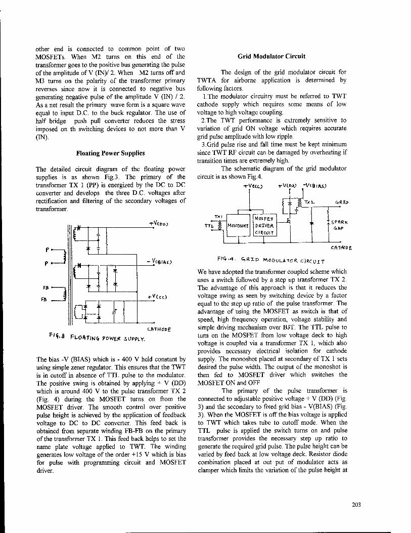
other end is connected to common point of two MOSFETs. When M2 turns on this end of the transformer goes to the positive bus generating the pulse of the amplitude of V (IN)/ 2. When M2 turns off and M3 turns on the polarity of the transformer primary reverses since now it is connected to negative bus generating negative pulse of the amplitude V (IN) / 2. As a net result the primary wave form is a square wave equal to input D.C. to the buck regulator. The use of half bridge push pull converter reduces the stress imposed on th switching devices to not more than V (IN).
Floating Power Supplies
The detailed circuit diagram of the floating power supplies is as shown Fig. 3. The primary of the transformer TX 1 (PP) is energized by the DC to DC converter and develops the three D.C. voltages after rectification and filtering of the secondary voltages of transformer.
FB . 3
t-Vct. t>>
CD ^8IAO
+-VCcc)
CA-THODE
'M FLOATING PC-WE* soppLy.
The bias -V (BIAS) which is - 400 V held constant by using simple zener regulator. This ensures that the TWT is in cutoff in absence of TTL pulse to the modulator. The positive swing is obtained by applying + V (DD) which is around 400 V to the pulse transformer TX 2 (Fig. 4) during the MOSFET turns on from the MOSFET driver. The smooth control over positive pulse height is achieved by the application of feedback voltage to DC to DC converter. This feed back is obtained from separate winding FB-FB on the primary of the transformer TX 1. This feed back helps to set the name plate voltage applied to TWT. The winding generates low voltage of the order +15 V which is bias for pulse with programming circuit and MOSFET driver.
Grid Modulator Circuit
The design of the grid modulator circuit for TWTA for airborne application is determined by following factors.
l.The modulator circuitry must be referred to TWT cathode supply which requires some means of low voltage to high voltage coupling.
2.The TWT performance is extremely sensitive to variation of grid ON voltage which requires accurate grid pulse amplitude with low ripple.
3.Grid pulse rise and fall time must be kept minimum since TWT RF circuit can be damaged by overheating if transition times are extremely high.
The schematic diagram of the grid modulator circuit is as shown Fig. 4.
TTL
cAtridHE.
FKi-4. C,R.XD MODULATOR. CIRCUIT
We have adopted the transformer coupled scheme which uses a switch followed by a step up transformer TX 2. The advantage of this approach is that it reduces the voltage swing as seen by switching device by a factor equal to the step up ratio of the pulse transformer. The advantage of using the MOSFET as switch is that of speed, high frequency operation, voltage stability and simple driving mechanism over BJT. The TTL pulse to turn on the MOSFET from low voltage deck to high voltage is coupled via a transformer TX 1, which also provides necessary electrical isolation for cathode supply. The monoshot placed at secondary of TX 1 sets desired the pulse width. The output of the monoshot is then fed to MOSFET driver which switches the MOSFET ON and OFF.
The primary of the pulse transformer is connected to adjustable positive voltage + V (DD) (Fig. 3) and the secondary to fixed grid bias - V(BIAS) (Fig. 3). When the MOSFET is off the bias voltage is applied to TWT which takes tube to cutoff mode. When the TTL pulse is applied the switch turns on and pulse transformer provides the necessary step up ratio to generate the required grid pulse. The pulse height can be varied by feed back at low voltage deck. Resistor diode combination placed at out put of modulator acts as clamper which limits the variation of the pulse height at
203
various PRF. The spark gap connected between the cathode and grid terminals does not allow the grid pulse to rise beyond predetermined value.
High Voltage Engineering Of Power Supply And Modulator
The power supply and modulator discussed above have to be housed in the least possible volume as well as reduction in weight was given enough consideration while fabrication of the modulator as this was developed for airborne application. Out of three submodules only DC to DC converter is placed on the low voltage deck. For the proto model floating power supplies were housed in a polypropylene box with dimension 12 cm x 20 cm x 10 cm. Apart from the power supply and modulator the same enclosure is used to accommodate the filament supply also. As this modulator box is to be floated on the cathode supply of order of-30 KV the selection of insulating material was very critical. Inclusion of filament supply has raised the problem of heat generated by diodes used for the development of filament voltage.
Ideally the use of transformer oil or fluorocarbon like FC-40 could have solved the problem of insulation as well as the heat sinking for the filament supply. Since this power supply and modulator is to be used for air borne application and ease of handling, the idea of liquid insulating material was abandoned. Hence the only option was to use solid potting compound. We have attempted to cast the modulator in a Dow Corning compound SYLGARD -184 which has electrical insulating strength of 550 V/mil but has relatively poor thermal conductivity 3.5 x 10"4cal /cm2/°C/cm. This has led us to the thermal breakdown inside the modulator box. Attempts were made to increase the thermal conductivity by adding mica powder to SYLGARD-184 during potting. Even this has not helped for thermal problem but it has added the weight to modulator box.
Ultimately the material which has given the best results were achieved by the use of Polybutadine material CB-1190 by M/S John C. Dolph. which has electrical strength same as that of SYLGARD -184 but the thermal conductivity of the order of 12.2x10" 4cal/cm2/°C/cm. This potting compound is available as 2 part compound which needs to be mixed in proper proportion before it is used for casting. During mixing there is every possibility of having air pockets inside the mixture due to gases generated because of exothermic reaction. These were eliminated by keeping this mixture under vacuum of the order of 10"5 torr. The best results were obtained when material is mixed and evacuated to
get rid of air pockets, then cast the module again under vacuum of the same order. Then the casted module is allowed to settle for 24 hours at room temperature. The settling time can be accelerated by baking the casted module at elevated temperature around50°C. This also ensures the removal of any moisture contents inside the box.
Test Results
Following are the resultsof the Power Supply and Modulator which was developed at our laboratory. The test was carried out on the capacitive load of 50 pF.
Grid Bias (Constant) - 400 V. Grid Pulse Height (Adj.) 500 to700 V Pulse Width 300 nS. Rise Time 22 nS. Fall Time 38 nS. Droop : 3%
Acknowledgments
Authors wish to thank Mr. P.B. Tole for continuos encouragement during the development of this Power Supply and Modulator. Also we would like to mention the contribution of Mr. Sen Mathews, Mr. T.N.Phadake and Mrs. K. M. Lobo for the realization of this design.
References
I. 'Low Noise High Power TWT Based Transmitter', Y.G.K.Patro, Sulabha Ranade, Sen Mathews, Shrikanth H, Sanjay M., Power Modulator Symposium 1992, June 23-25, South Carolina, PP 77-78.
2 'High Frequency Power Supplies Theory and Design',Chapter 3, George C. Chrysis,Published by Mc GrawHill.
3 'Switch Mode Power Supplies Hand Book',Part II, Chapter 12,Keith Billings,Published by Mc Graw Hill.
204
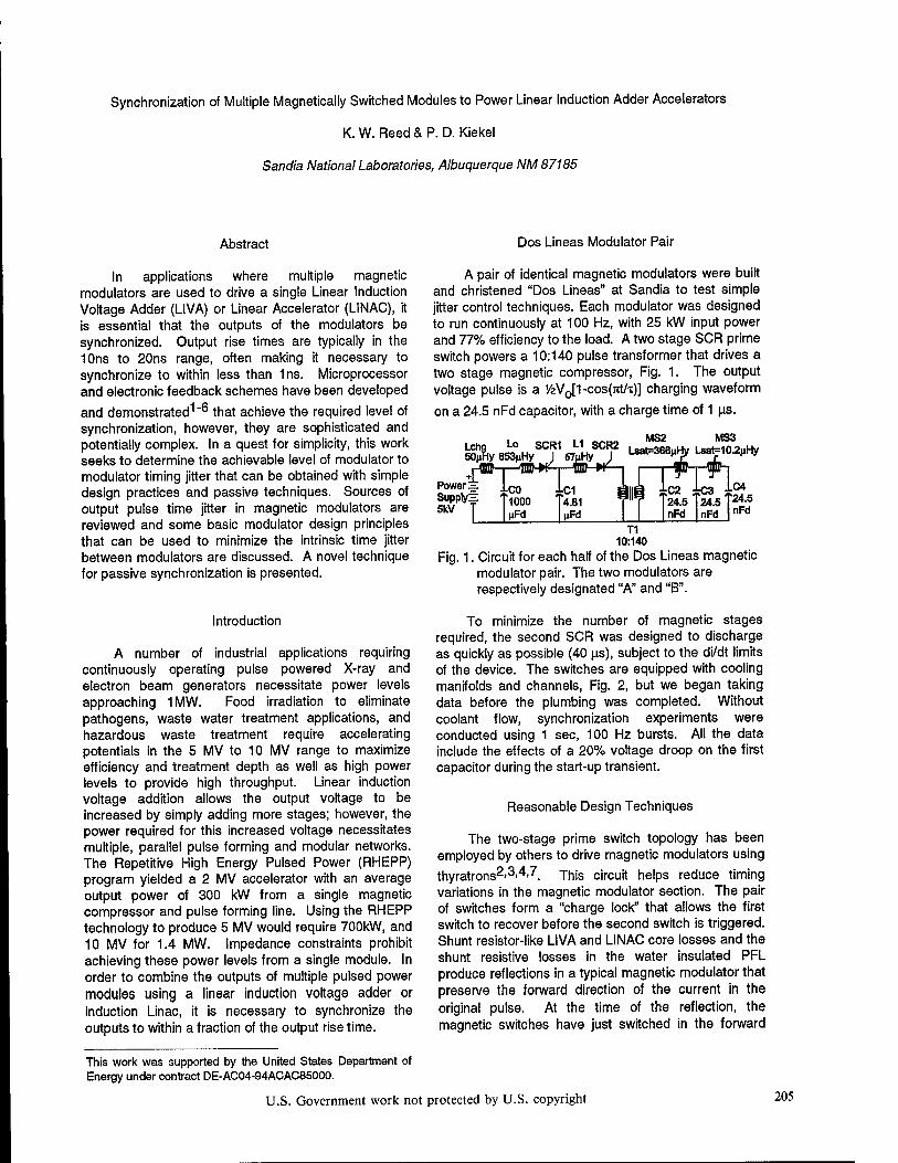
Synchronization of Multiple Magnetically Switched Modules to Power Linear Induction Adder Accelerators
K. W. Reed & P. D. Kiekel
Sandia National Laboratories, Albuquerque NM 87185
Abstract
In applications where multiple magnetic modulators are used to drive a single Linear Induction Voltage Adder (LIVA) or Linear Accelerator (LINAC), it is essential that the outputs of the modulators be synchronized. Output rise times are typically in the 10ns to 20ns range, often making it necessary to synchronize to within less than 1ns. Microprocessor and electronic feedback schemes have been developed
and demonstrated^ "^ that achieve the required level of synchronization, however, they are sophisticated and potentially complex. In a quest for simplicity, this work seeks to determine the achievable level of modulator to modulator timing jitter that can be obtained with simple design practices and passive techniques. Sources of output pulse time jitter in magnetic modulators are reviewed and some basic modulator design principles that can be used to minimize the intrinsic time jitter between modulators are discussed. A novel technique for passive synchronization is presented.
Introduction
A number of industrial applications requiring continuously operating pulse powered X-ray and electron beam generators necessitate power levels approaching 1MW. Food irradiation to eliminate pathogens, waste water treatment applications, and hazardous waste treatment require accelerating potentials in the 5 MV to 10 MV range to maximize efficiency and treatment depth as well as high power levels to provide high throughput. Linear induction voltage addition allows the output voltage to be increased by simply adding more stages; however, the power required for this increased voltage necessitates multiple, parallel pulse forming and modular networks. The Repetitive High Energy Pulsed Power (RHEPP) program yielded a 2 MV accelerator with an average output power of 300 kW from a single magnetic compressor and pulse forming line. Using the RHEPP technology to produce 5 MV would require 700kW, and 10 MV for 1.4 MW. Impedance constraints prohibit achieving these power levels from a single module. In order to combine the outputs of multiple pulsed power modules using a linear induction voltage adder or induction Linac, it is necessary to synchronize the outputs to within a fraction of the output rise time.
Dos Lineas Modulator Pair
A pair of identical magnetic modulators were built and christened "Dos Lineas" at Sandia to test simple jitter control techniques. Each modulator was designed to run continuously at 100 Hz, with 25 kW input power and 77% efficiency to the load. A two stage SCR prime switch powers a 10:140 pulse transformer that drives a two stage magnetic compressor, Fig. 1. The output voltage pulse is a 1/2V0[1 -cos(irt/i)] charging waveform
on a 24.5 nFd capacitor, with a charge time of 1 us.
■ - nnnJ i A *.*•***#>. MS2 MS3
Fig. 1. Circuit for each half of the Dos Lineas magnetic modulator pair. The two modulators are respectively designated "A" and "B".
To minimize the number of magnetic stages required, the second SCR was designed to discharge as quickly as possible (40 us), subject to the di/dt limits of the device. The switches are equipped with cooling manifolds and channels, Fig. 2, but we began taking data before the plumbing was completed. Without coolant flow, synchronization experiments were conducted using 1 sec, 100 Hz bursts. All the data include the effects of a 20% voltage droop on the first capacitor during the start-up transient.
Reasonable Design Techniques
The two-stage prime switch topology has been employed by others to drive magnetic modulators using
thyratrons2'3'4'7. This circuit helps reduce timing variations in the magnetic modulator section. The pair of switches form a "charge lock" that allows the first switch to recover before the second switch is triggered. Shunt resistor-like LIVA and LINAC core losses and the shunt resistive losses in the water insulated PFL produce reflections in a typical magnetic modulator that preserve the forward direction of the current in the original pulse. At the time of the reflection, the magnetic switches have just switched in the forward
This work was supported by the United States Department of Energy under contract DE-AC04-94ACAC85000.
U.S. Government work not protected by U.S. copyright 205
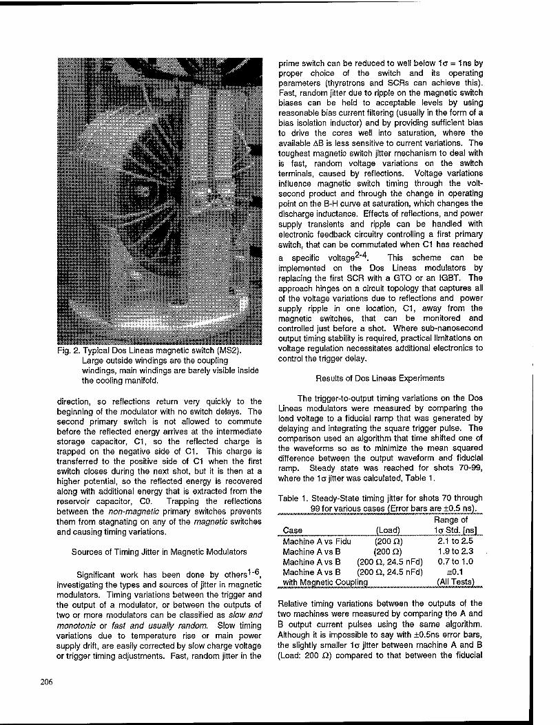
Fig. 2. Typical Dos Lineas magnetic switch (MS2). Large outside windings are the coupling windings, main windings are barely visible inside the cooling manifold.
direction, so reflections return very quickly to the beginning of the modulator with no switch delays. The second primary switch is not allowed to commute before the reflected energy arrives at the intermediate storage capacitor, C1, so the reflected charge is trapped on the negative side of C1. This charge is transferred to the positive side of C1 when the first switch closes during the next shot, but it is then at a higher potential, so the reflected energy is recovered along with additional energy that is extracted from the reservoir capacitor, CO. Trapping the reflections between the non-magnetic primary switches prevents them from stagnating on any of the magnetic switches and causing timing variations.
Sources of Timing Jitter in Magnetic Modulators
Significant work has been done by others1"6, investigating the types and sources of jitter in magnetic modulators. Timing variations between the trigger and the output of a modulator, or between the outputs of two or more modulators can be classified as slow and monotonic or fast and usually random. Slow timing variations due to temperature rise or main power supply drift, are easily corrected by slow charge voltage or trigger timing adjustments. Fast, random jitter in the
prime switch can be reduced to well below 1a = 1ns by proper choice of the switch and its operating parameters (thyratrons and SCRs can achieve this). Fast, random jitter due to ripple on the magnetic switch biases can be held to acceptable levels by using reasonable bias current filtering (usually in the form of a bias isolation inductor) and by providing sufficient bias to drive the cores well into saturation, where the available AB is less sensitive to current variations. The toughest magnetic switch jitter mechanism to deal with is fast, random voltage variations on the switch terminals, caused by reflections. Voltage variations influence magnetic switch timing through the volt- second product and through the change in operating point on the B-H curve at saturation, which changes the discharge inductance. Effects of reflections, and power supply transients and ripple can be handled with electronic feedback circuitry controlling a first primary switch, that can be commutated when C1 has reached
a specific voltage2"4. This scheme can be implemented on the Dos Lineas modulators by replacing the first SCR with a GTO or an IGBT. The approach hinges on a circuit topology that captures all of the voltage variations due to reflections and power supply ripple in one location, C1, away from the magnetic switches, that can be monitored and controlled just before a shot. Where sub-nanosecond output timing stability is required, practical limitations on voltage regulation necessitates additional electronics to control the trigger delay.
Results of Dos Lineas Experiments
The trigger-to-output timing variations on the Dos Lineas modulators were measured by comparing the load voltage to a fiducial ramp that was generated by delaying and integrating the square trigger pulse. The comparison used an algorithm that time shifted one of the waveforms so as to minimize the mean squared difference between the output waveform and fiducial ramp. Steady state was reached for shots 70-99, where the 1 a jitter was calculated, Table 1.
Table 1. Steady-State timing jitter for shots 70 through 99 for various cases (Error bars are ±0.5 ns)
Range of Case (Load) 1aStd.j[ns] ..(Loacj), Machine A vs Fidu (200 Q) 2.1 to 2.5 Machine A vs B (200 Q) 1.9 to 2.3 Machine A vs B (200 O, 24.5 nFd) 0.7 to 1.0 Machine A vs B (200 Q, 24.5 nFd) =0A with Magnetic Coupling (All Tests)
Relative timing variations between the outputs of the two machines were measured by comparing the A and B output current pulses using the same algorithm. Although it is impossible to say with ±0.5ns error bars, the slightly smaller 1a jitter between machine A and B (Load: 200 Q) compared to that between the fiducial
206
and machine A, may indicate that voltage ripple effects on the common reservoir capacitor, CO, tend to cancel when the outputs are compared to one another. A better matched load (200Q, 24.5 nFd) reduced the reflections and yielded even lower output jitter. In any case, the 1a steady state time jitter seems to be remarkably small for a pair of modulators that have no jitter compensation circuits and are running from an unregulated power supply. This performance is attributed to ample, well filtered magnetic switch biases and the reflection trapping primary switch topology. The only likely source of time variation in the outputs of the machines is voltage variations on C1. These voltage variations are due to a combination of power supply ripple, start-up transients and the captured load reflection. The voltage was measured on C1 just before the second SCR switched and then converted to the output time change that it would cause using,
■[tsw-(tfB)sin(msv/t)]n
At0Ut=AvCl£-
shown in Fig. 3. The initial advancement in the output time corresponds to an increase in the charge voltage on C1 at the onset of repetitive operation, due to energy recovery. The voltage on C1 increases most between the first and second shots and then continues to increase more slowly as the higher input charge causes a proportionate increase in the reflection. The voltage and hence the output timing advance falls off as the voltage drop in the wires between CO and the charging power supply begin to dominate.
n VCi [1 - cos(7rtsw/T)]n
SWITCH WINDINGS - Fig. 4. The Magnetic Coupling Technique
lsw
= compression stage index = time to peak = time to switch
Atout = output time shift
VQ-| = voltage on C1
AVQ-| = change in VQ-) causing output time shift.
yielding a scale factor of At0Ut/AVc1=2.6 ns/volt. The
time jitter calculated from the voltage ripple on C1 from two different burst runs was 1a = 1.6ns & 2.0ns compared to the measured time jitter of 1a = 2.1ns & 2.1ns. Furthermore, the decay time constant of 2.6xVC1 matched the time constant of the output delay exactly. This indicates that to within our ability to measure, the output time variations are due to voltage variations on C1. If there are other jitter components such as trigger jitter in the SCRs, they are very small.
A typical plot of the timing variation between the output of one of the modulators and the fiducial is
TIM
E S
HIF
T C
OM
PA
RE
D T
O F
IDU
[nse
c]
8
8
8
S
8
S
-750-
-760- a flrf
/ '
, / -780-
-790
/ r / u 70 80 90 100
I I
3 20 40 60 80 100
SHOT NUMBER
Fig. 3. Output timing variation on machine A relative to the fiducial. Inset is detail of shots 70 to 100.
Synchronization by Magnetic Coupling
A simple, passive, maintenance free technique for synchronizing independent magnetic switches and modulators has been developed. Two similar magnetic switches can be made to switch together by applying equal windings to both and then interconnecting them symmetrically, Fig. 4. No current flows in the coupling winding if the switches charge together and switch together. If one switch starts to charge before the other, the transformer action of the coupling winding causes the other switch to begin to charge as well. This tends to equalize the charge voltage on corresponding stages of both modulators. If then for any reason at all one switches before the other, the coupling winding acts as a shorted secondary on the slow switch and forces it into a low inductance or switched state. Ten-turn coupling windings were installed between machines A and B on corresponding switches of both magnetic compression stages. The output timing offset between the Dos Lineas modulators is compared with and without magnetic coupling in Fig. 5. The start-up timing transient without magnetic coupling is mainly due to the voltage transient on CO varying the output timing via the constant volt- second product. There is a small residual start-up transient with magnetic coupling that is believed to be caused by modulation of the saturated inductance's in the output switches due to the variation in the operating point. The varying inductance's change the widths of the output current pulses that we are comparing resulting in the timing offset. Since minimizing the RMS difference yields the time shift that centers the current pulses on each other, a relative width change on pulses that are forced to start at the same time by
207
0-
-100-
■jr -200 ■ i !| -300- CO UJ 2 F -400-
-500-
fWwHOWWOUnoooo.1.»
MAGNETIC .< X
COUPLING |NO COUPLING|
f ■--~-~~ \ -70.0 -
-71.0-
-720-
-73.0 -
\ JfA $ A \\ V
50 70 90 -600 J
( ) 20 40 60 80 100
SHOT NUMBER
Fig. 5. Effect of magnetic coupling on transient and on random jitter between Dos Lineas outputs. Inset shows expanded view of shots 50-100. (Uncoupled data was shifted up in inset)
the magnetic coupling, causes an apparent time shift to result from our algorithm.
In addition to comparing transients and jitter with and without coupling, two additional tests were conducted to evaluate magnetic coupling effectiveness. First, trigger offsets were introduced between the two machines of ±1us and second a 6.5% difference in charge voltage was introduced at the inputs of the two machines. As indicated in Table 1, in all of these tests the measured time shifts between the outputs with coupling were identical to the baseline results, with coupling, in Fig. 5.
With magnetic coupling, we found that in all of our tests the timing on the A output is locked to 70 ns before the B output. This fixed time shift is due to the round-trip propagation delay in the coupling circuit. This was determined by calculations for a helical transmission line with the ground housing far from the helical winding, yielding an approximate round-trip
delay of 62 ns for the coupling winding**. The saturated inductance of the first magnetic switch on the A side is slightly less than that on the B side. Since these switches are coupled, they switch together and the A side always reaches the volt-second product of the A output switch first. Thus, regardless of whether machine A is triggered before or after B, the A output always leads the B output by the fixed geometrical delay in the coupling winding between the output switches ~ give or take the apparent delay caused by modulation of the saturated inductance's in the output switches. On different days, our operating point varied enough to make this time shift between machine A and B vary by a total spread of 3.5 ns across all of our data.
When there is an imbalance between the two machines, the first stage to be affected by the imbalance transmits a small current (15 A in the first coupling network for a 1 us trigger offset) through the coupling network to the next down stream stage. If the next stage is magnetically coupled this current has no effect and it is shunted through that stages coupling
network, and so on. To test the effect on the timing of an uncoupled switch being driven by the modulator, we uncoupled the second magnetic switch pair (its hold-off time is 6.7 LIS), leaving the first pair coupled and introduced a trigger offset between the machines that ranged from -100ns to 100ns. In response to the foot, the timing variation at the output of the uncoupled switch ranged from -4ns to 4ns. This timing represents 0.06% of the hold-off time of the uncoupled switch, to which it is proportional. In an actual application, the first switch that might be difficult to couple would be a closed geometry switch with a hold-off time of about 1us. Thus, the ±100 ns trigger offset would result in ±0.6ns output timing variation. PSPICE simulations indicate that this offset can be greatly reduced by increasing the bias on the uncoupled switch to compensate for the volt-seconds applied by the foot.
Conclusions
The Dos Lineas modulator pair has been used to demonstrate that it is possible to build a pair of magnetic modulators that have less than 1a = 1 ns steady-state timing jitter between their outputs, with no special jitter compensation provisions. Attainable jitter is a function of the load. If start-up transients are an issue, they can be compensated using voltage regulation as shown by others or magnetic coupling. Magnetic coupling shows promise as a simple maintenance-free way to control all types of machine- to-machine jitter in magnetic switches and modulators.
References
1. R. N. Hitchcock, "Variable Magnetic Switch Design and Control in Repetitive Systems", 1992 20"" Power Modulator Symp., CH3180-7/92/0000-0201, pp. 201-204.
2. M. A. Newton, et al., "Design and Testing of the 5kHz, 3MW Thyratron Modulators for ETA II", 1988 IS"1 Power Modulator Symp., pp. 71-74.
3. M. A. Newton & J. A. Watson, 'Timing and Voltage Control of Magnetic Modulators on ETA II", 7th
IEEE Intl. Pulsed Power Conf., 1989, pp.175-177. 4. J. A. Watson, et al., "Precision Voltage Regulation
on the 5kHz, 3.125 MW ETA-II Pulsed Power System", 8'" IEEE Intl. Pulsed Power Conf., 1991, pp. 221-223.
5. M. A. Newton, et.al., "The Power Conditioning System for the Advanced Test Accelerator", 1982 Fifteenth Power Modulator Symp., pp. 333-337.
6. E. G. Cook, et al., "High Average Power Magnetic Modulator for Copper Lasers", 8'" IEEE Intl. Pulsed Power Conf., 1991, pp.537-542.
7. S. Ashby, et al., "CLIA-A Compact Linear Induction Accelerator System", 8'" IEEE Intl. Pulsed Power Conf., 1991, pp. 940-942.
8. Reference Data for Radio Engineers, Howard W. Sams & Co., Inc., 6,h Addition, 1981, pp. 24-27.
208
Capacitors - Past, Present, and Future: A Trans-National Perspective
W. J. Sarjeant SUNY/AB, Buffalo, NY
R.E. Dollinger SUNY/AB, Buffalo, NY
J. Zirnheld SUNY/AB, Buffalo, NY
F.W. MacDougall Aerovox, Inc.
New Bedford, MA
and H. Goldberg SUNY/AB, Buffalo, NY
Abstract — Over the last decade, significant increases in capacitor reliability have been achieved through a combination of advanced manufacturing techniques, new materials, and diagnostic methodologies to provide requisite life-cycle reliability for high energy pulse applications. Recent innovations in analysis of aging, including dimensional analysis, are introduced for predicting component performance and fault tolerance.
Introduction
As the military and commercial requirements for compact electrical power systems grow substantially over the next decade, development of high power/energy density capacitor technology is a major enabling technology component element. For microsecond to fractional-second electrical energy storage, discharge, filtering and power conditioning, capacitor technology is unequalled in flexibility and adaptability to meet a broad range of requirements in the future. "
Today, high-energy pulsed power conditioning has been achieved for pulse durations from 0.05 out to over 1,000 microseconds, at voltages from megavolt levels for microseconds, down to subkilovolt levels at the longer pulse durations.3"5'9'10'12'19'20 Voltage levels have been determined by the nature of the load. Developing innovative new capacitor and related insulation systems operating at near ultimate voltage withstands (> lOx to 15x today's operational levels), would enable the achievement of lightweight systems needed in the future. " Repetition rates could be up to sub-Megahertz, necessitating integrated development of capacitor technology with that of negligible-loss switching topologies and voltage multiplication transformers.1"
Description of the Technology
A capacitor generally consists of conducting plates or foils separated by thin layers of an insulating medium, with the plates on the opposite sides charged by a voltage source; the resultant electrical energy of this charged system is stored in the polarized insulating medium. Capacitors permit electrical energy to be stored over a long charging time and then released as required over very short (submicroseconds to multimilliseconds) periods, under controlled conditions. ' Such energy discharge operation, as with filtering duty, requires device technology of very high efficiency per unit volume/mass to minimize thermal management constraints upon the system designer . ' ' ' Particular attention must be given to the life and reliability necessitated
by the system requirements, with the main classes of capacitors being •11 t I A- -r ui 1 7,8,11,14,15 illustrated in Table 1.
Table 1
Main Classes of Capacitor Applications
* Low and high frequency filtering in ac + dc systems * AC resonant-charging power supplies * Switched-mode power supplies * Energy discharge * High frequency bypass
Most systems are projected to be divided by voltage/average power/run-time considerations as shown in Table ' "' ' '
Scalability of Capacitor Technology
Capacitors for AC ripple filtering in DC systems, passive energy storage and power transfer, are unequalled in their flexibility of geometry, permitting rapid design optimization for man-portable, vehicular, and large mobile or fixed ground installations for voltages from sub-kilovolts to megavolts, allowing rapid turn-around time and modular field maintenance.7"19 For future users of advanced power sources, the compact systems needed would be enabled with capacitor energy and power densities ten (lOx) to one hundred (lOOx) times those available today.1"15'19 This is potentially feasible, and, should be conjoined with the possibility of developing advanced capacitor technologies that could well yield capacitors whose performance degraded gracefully, hence, no longer being a single point of failure within a power conditioning system.7'8'13'1 '21 Indeed, even during normal life and under adverse environments, such a technology would always result in graceful and predictable reduction in performance so that total system operation could be retained at reduced performance levels.7'14'/2
Table 3 projects near term and future performance of state-of-the-art capacitor technology and shows selected examples of several classes of advanced capacitors that R&D could turn into future practical, highly compact systems.1"19 These advanced systems all have the potential for elevating the energy (kJ/kg) and power (kW/kg) densities by a factor of 10 to 100 times. Costs for these advanced units is projected to be comparable to current technology, in production volumes. 7,13,14,19
0-7803-3076-5/96/S5.00 © 1996 IEEE 209
The observed evolutionary advance rate for capacitor technology is about a factor of 2x per decade in any performance factor well away from natural limits (e.g., such as power density).2'3'7'19 This rate is projected then to meet the requirements that the capacitor volume no longer be a substantial portion of the total volume of the power source system, to meet such power and energy capacitor energy densities between the years of 2065 and 2075 of the next century. ,8 On the
other hand, the current advance rate in supported R&D for high-energy pulse-discharge capacitor technology for high energy capacitor systems projects to eighteen (18x) times per decade, which when applied to the other types of capacitors needed in next generation power systems, projects to meeting these far-term requirements by the end of this
3 6 7 11 13 15 19-22 decade, provided the necessary R&D is set in place. ••••••
Table 2.
Capacitor Applications and Operating Conditions
Power
kW (average)
Voltage
kV (peak)
Run-Time
seconds
<1
1-10
10-1000
>100
<50
<100
<500
>100
>1000
>10
>100
>100
Application
* Electronic Counter-Measures * LADAR * Communications * Microcomputers
* LADAR * RADAR * Computers
* High Power Microwaves * RADAR * Power Quality * Distributed Power Systems
* Directed Energy Weapons * Anti-Mine * VAR Stabilization * Power Factor control * Industrial processing
Competitiveness Advantages of Higher Power Density Capacitor Technology
A major factor in designing the next generation of advanced power conditioning systems and switched-mode power supplies is the selection of available high power density components for use therein. 7,14,15,18,19 observations over recent years have shown that a technically highly demanding area is the application of capacitors for switched-mode power supplies and switching regulators, mainly in the areas of DC input and output filtering, as well as resonant elements internal to the power conditioning system.2'8'11'14 Only with adequate data on compact (at least 5 to 10 times higher power density) capacitors, performing at the higher frequencies of interest (» 100 kHz) can cost-effective designs of such power systems be practical for both the international market place, as well as for domestic use.7'14'15'21'22 Ceramics presently appear to be one intrinsically high- temperature, and hence long-lived, technology available that has a very large potential for advancement, particularly with the recent advent of new materials and the Multilayer Ceramic Capacitor (MLC) demonstrated production capacitance and voltage scalability (»100 ^F>500WVDC).n'21'22
The development of new solid and liquid materials, in conjunction with advanced methods of manufacturing technology, is feasible with tools emerging from present successful technology programs. "' What will be required is a tightly integrated material/component set of development programs tailored to areas of need for the main classes of capacitor technology.7'19'20 The advancement of capacitor technology to date has been successful only because of the preeminent role that the capacitor developers in industry have directly taken in this integration of materials development into the practical realization of advanced capacitors.7'19 The Power Source developers of the future may well desire to support a systems-responsive technology base development program in each of the major capacitor technology areas, resulting in demonstration subscale hardware that will operate at the power and energy densities needed, being no smaller than tenth-scale in unit capacitance.4"9 The projected increase in power density of ceramic capacitors for use in Switched-Mode Power Supplies is widely discussed.'2'8-13-15 Achieving the power density of between 10 and 20 MVAR per cubic meter would mean that the capacitor volume fraction in such systems is reduced from the 30% to 50% of today, to negligible proportions (5%). ' "
210
Completing such a program would reduce the capacitor volume/mass-fraction in envisaged systems sufficiently (i.e., by more than a ten-fold reduction in capacitor volume fraction in advanced
power systems) so that constraints from this technology on system feasibility would be removed.4"9'19'21
Table 3
Performance of State-Of-The-Art And Advanced Capacitor Systems
Capacitor kJ/kg kW/kg Rep-Rate Main Issues System Now/Future Now/Future Hz
Polymer Film: 0.4/20 5/20 k > 100 * New Polymer Films * Impregnants * Foils and Conductors *>200°C * » 1 kJ/unit * Voltage Reversal * Pulse Duration * Repetition Rate
Ceramic: 0.01/5 10/10 k >100k * Ceramic Formulations * Electrodes *>200°C * 1 kJ/unit * Voltage Scaling * Fusing
Electrolytic: 0.2/2 2/10,000 > 100 * Electrolytes * Separators *>200°C * 1 KJ/unit * Gassing * Hermetic Sealing * Voltage Reversal * Pulse Repetition Rate
Mica: 0.005/0.05
The Future
5/50 k >lMHz
+
* Electrodes *>300°C * 1 kJ/unit * Voltage Scaling/ Reversal * Materials * Impregnants
CAPACITOR TECHNOLOG HIQH ENERGY STORAGE TYPE
Achieved ■ Projected
Fig. 4 shows the timeline of increasing energy density in energy discharge capacitors, starting from the early 1960's.18"23 Metallized technology capacitors from U.S. industry have been in the field for several years, at energy densities of 0.5 -1.5 KJ/Kg.
Projections of energy densities beyond these levels will only be as accurate as fundamental research in dielectrics moves into the arena where energy density is indeed one of the material parameters investigated.
Summary
The very difficult technical challenges described in the introduction to this report, in the view of the committee, can be accomplished or at least approached if a five-year research and development program were to be established at a few major Universities and Government Laboratories, with appropriate industrial guidance and participation. The major business issues are listed just following Fig. 1.
10'
??? Nature's Limit ???
10'
U
10» ,<* f
10'' si'
it-
>-
New Metallized
Technology -r ,
1970 19S0 1990 2000 2010 2020
Fig. 1. Shows the timeline of increasing energy density in energy discharge capacitors, starting from the early 1960's.
211
The major business issues are as follows:
1. At some point, the capacitor business must make a profit and profit must provide a competitive return on investment.
2. Major suppliers to U.S. capacitor industry elements are off- shore, and we therefore must convince U.S. materials corporations to invest in appropriate domestic based film manufacturing facilities.
3. OEMs who use (i.e., buy) capacitors are very rapidly moving to the Far East, China, India, Malaysia, Korea, and Indonesia. Capacitor plants that serve these countries due to low cost, short lead times, etc., must also be located in the Far East.
As is evident, a number of issues appear, but no root problem, and no solution. R&D can be accomplished, but it may not generate a growing capacitor business in the U.S.
In sum, the next market penetration opportunities in the capacitor areas will be little different from those in the advance computer arena - that is to say some market fraction will be dominated by technological superiority, balanced by the rest overcome through market dominance via low cost production.
Acknowledgment
The authors wish to extend their appreciation to their colleagues at Aerovox, students at the High Power Electronics Institute of the State University of New York at Buffalo, and members of the technical staff of the Lawrence Livermore National Laboratory, for their technical assistance and to the organizations for permission to use this information in>this capacitor technology advances report. Ongoing technical discussions with D. Duston of BMDO, C. Le Gressus of the Centre d'Etudes de Bruyeres-Le-Chateland and G. Blaise of the Universite Paris-Sud, Laboratoire de Physique des Solides, are most appreciated.
References
1. "R&D Subcommittee Report on Capacitors - 1995, "Power Sources Manufacturers Association, 14 Ridgedale Ave., Suite 125, Cedar Knolls, N.J. 07928, tel. 201-538-9170.
2. Power Electronics Conference, Long Beach Convention Center, Long Beach , California, February 13-16, 1990.
3. "Briefing to the Defensive Technologies Study Team on Space Power Technology," by W.J. Sarjeant, Institute for Defense Analysis, Washington, DC, June 15, 1989 (unpublished).
4. W.J Sarjeant and R.E. Dollinger, High Power Electronics, TAB Professional and Reference Books, Inc., New York, May, 1989.
5. I. Vitkovitsky,/%/2 Power Switching, VanNostrand/Reinhold Inc., New York, March, 1988.
6. SDI-SLKT/AF Space Power Architecture Studies and summaries by the Independent Evaluation Group, especially D. Furgal, "Power Conditioning for Multimegawatt Space Power Systems," SNL, June, 1989.
7. "Advanced Power Sources for Space Missions," NAS-NRC (EEB) Committee on Advanced Spaced Based High Power Technologies Report #ADVPOW, National Academy Press, May, 1989.
8. "Mobile Electric Power Technologies for the Army of the Future - Engines, Power Sources and Electrical Aspects," NAS-NRC (EEB) Committee on Mobile Electric Power Plant Technologies Energy Engineering Board, Commission on Engineering and Technical Systems Report, June, 1988.
9. T.R. Burkes and W.J. Sarjeant, "Discussion Paper on SDI Power and Power Conditioning Components," unpublished study paper for the NAS-NRC (EEB) Committee on Advanced Space Based High Power Technologies, August 31, 1987.
10. T.R. Burkes, "A Critical Analysis and Assessment of High Power Switches," Naval Surface Weapons Center Report NP30/78, September, 1978.
11. Olean Advanced Products, Technical Catalogue # 10875OAP, 1989.
12. J. Ennis, "High Energy Capacitor Development," Symposium presented at the High Power Electronics Institute of the State University of New York at Buffalo, November, 1986.
13. G.R. Love, "Energy Storage in Ceramic Dielectrics," Sprague Technical Paper TP87-4, American Ceramic Society Spring Meeting, Pittsburgh, PA, April, 1987.
14. "Selection and Application of Capacitors," J.D. Moynihan, Editor-in-Chief, Second Edition, Components Technology Institute Report, 1987. Available from CTI, 904 Bob Wallace Avenue, Suite 117, Huntsville, AL 35801, tel. 205-536-1304
15. "Capacitors for Switching Regulator Filters," Electrocube Technical Bulletin No. 13, 1987.
16. J.J. Svec, "Capacitors from 0.01 Ounce to 50 Pounds," Ceramic Industry, August, 1979, pp. 32-34.
17. "Development of an 1100 °F Capacitor," NASA reports NASA-CR-1213 (1968) and NASA-CR-1799 (1971).
18. W.J. Sarjeant, "Capacitor Fundamentals," Proceedings of the 1989 IEEE Electrical Insulation Conference," Chicago Hyatt O'Hare, Chicago, III, September 24-28, 1989, pp. 1-51.
19. "The Department of Defense Critical Technologies Plan," for the Committee on Armed Services, United States Congress, Marchl5, 1992.
20. J.R. Laghari and W.J. Sarjeant, "Energy Storage Pulsed Power Capacitor Technology," Proceedings of the IEEE Power Sources Symposium, Cherry Hill, N.J., June 25-28, 1990.
21. "Ad Hoc Workshop On Power Conversion Technology in the Year 2000," Organized by R.S. Freund, Report Prepared by D. Staffiere, Sponsored by the IEEE Power Electronics Society and the Power Sources Manufacturer's Association, May, 1994.
22. E. Motto and Ml Gebbia, "Snubber Capacitor Size and Characteristics Affect High Power IGBT Module Performance," Power Conversion and Intelligent Motion, June, 1994, pp. 10-18.
23. D. W. Larson, F. W. MacDougall, X. H. Yang, and P. E. Hardy, "The impact of high energy density capacitors with metallized electrodes in large capacitor banks for nuclear fusion applications," Proceedings of the 9th IEEE Pulsed Power Conference, Albuquerque, NM, June 22-25, 1993.
212
High Power Harmonic-Free AC to DC Rectification
R. Limpaecher, R. Rodriguez, M. Bush, K. Vinacco & M. Gatewood D.C. Transformation, Inc.
181 Elliott Street Beverly, MA 01915
Abstract - The Sequential Discharge Rectification (SDR) [1][2][3][4] system is a regulated high power AC to DC converter, producing a DC output with no VAR and harmonics generation. The technology is based on the property of resonance circuits, thereby permitting the use of soft switching and self commutating low dl/dt solid states devices. The switching characteristics permit the utilization of less expensive thyristors available in high voltage, high current and high power ratings.
The new circuit topology allows the energy extraction from any phase to be proportional to the square of the instantaneous line voltage. The energy extraction, performed at constant intervals, will load the AC line to the desired power level over the entire AC cycle. Since the load which the SDR technique imposes on the multiple phase inputs is equivalent to a resistive load, it produces no VAR and harmonic distortions that must be filtered out. The rectification approach of this invention includes about the same number of components as a conventional bridge rectification approach. The low dl/dt permits the utilization of high voltage high power thyristors for megawatt power applications. Test data will be presented for a 144 kW AC to DC demonstration system producing a dual low ripple DC output of ± 260 VDC. The output can be regulated, its fault current protected, with a turn-on and turnoff of about 2-3 msec and complies with the harmonic requirements imposed by the IEEE 519-1992 and EC 555-2 specifications.
L INTRODUCTION This paper describes a new circuit topology that
permits efficient harmonic-free rectification, at near unity power factor.
Due to the proliferation of nonlinear industrial and consumer loads, industry standards have been formulated to limit harmonics in power systems and to encourage the development of electrical loads that generate no harmonics. Two such standards are the EC 555-2 and the IEEE 519-1992. These standards have been revised to establish new recommended limits on the level of harmonics that users can inject into the electrical grid. With the SDR technology, industrial and consumer equipment would meet and exceed these new specifications without the use of additional filtering equipment.
In an effort to evaluate and test the SDR technology, a demonstration circuit was designed and tested at a power level in excess of 100 kW, in a + 260 VDC dual power supply configuration. The electrical schematic for the demonstration circuit is shown in Figure 1. This figure will be used as an introduction to the SDR circuit theory and operation of the demonstration experiment.
**t-
Figure 1. SDR Schematic Diagram
Input power to the circuit is derived from six single phase, 50 kVA step-down power transformers. The six transformers, with an input phase voltage of 580 VAC are wired together so that their secondary windings form two separate 'Y' connections. The two Y's are connected such that they are 180 degrees out of phase, to yield the six input phases, 60 degrees apart, with a line voltage of 380 VAC, as shown in Figure 2.
PHASE ANQLE IP T >BD° fl£P TO 12CP tar TO 18tP 18tPTO240° 24tP TO 300° 300° TO 300°
POSITIVE CHARGE SCR« PI1. Pli.PlB PI1.PI2.PI« PI1 PI2.PI3 PI2. PI3.PH PI3 PH.PI5 PH.PiS.P«
NEGATIVE CHARGE B Cft. PIZ-2. PI3-3, P13-3, PM-4, P15-5
PM-4, PI5-5. pte-e
PI1-1.PI5-5. pie-e
PM-1.PI2-2, Plfl-8
PI1-1.PI2-2. PI3-3
'- T~"\ .. ! / " ',/ ... T\
1 V7 1 \ V3 | \
1 ; \ \ ! ) \
vs ! / V8
! / • M
V « 1\ *» i \
POSIT fVE DI8CHARQE
.,- Po3 Po2 Pol
Po3 Pol Po2
Pol | Pol Po3 Po2 Po2 i Po3
Po2 Po1 Po3
1 Po2 Po3
1 Po1
Po3 ! Po3 Po2 Po1 Po1 i Po2
Po3 Po2
| Po2 1 Po3
Po2 ' Po2 Pol Po3 Po3 i Po1
DISCHARGE SEQUENCE Pod
Po4 Po5
PoB ' Po5 Po5 , Pofl
Po5 P04
I Po5 1 PoB
P04
poe i Poe
P04 ] P05
Po« PoB PoS
I PM ] Po5
PoS 1 Po5 Pod ' PoB PoS Po4
Figure 2. Input Phase Voltages & Firing Sequences
0-7803-3076-5/96/S5.00 © 1996 IEEE 213
The control system for the SDR demonstration experiment consists of three main elements. The programmable logic controller (PLC), as depicted in Figure 3, is responsible for facility operations. Slow speed tasks such as high voltage contactor actuation, water circulation pump control, and safety interlock monitoring are delegated to the PLC. An embedded microprocessor (ADSP 21020) interfaces with a graphical user interface (GUI), analog and digital I/O, and a microcontroller (Motorola 68332). The analog module collects data for display on the GUI or for process control. The digital module is used to communicate control and status information with the experiment under test. The microcontroller supplies synchronized pulse trains to the SCR trigger system. Each of the SCRs is triggered individually from a signal transmitted from the 68332. These signals are fiber optically coupled to the respective trigger boards. Control of the timing parameters between these signals IS passed through the GUI to the 21020 and into the 68332.
Through the analog input module, the embedded microprocessor continually monitors the input and output conditions and regulates the pulse repetition rate of the SCRs to compensate for variations in the load.
Figure 3. Rectification Control System
The health of the system under test is continuously monitored by the embedded microprocessor through the digital I/O module. Current waveforms from critical locations in the circuit, are transmitted through fiber optic cables from self-powered current transformers (CTs). The control system scans for a fault condition every 10 microseconds, which gives the system the ability to interrupt operations within that time frame. Given the appropriate control algorithm and topology, the PCS devices can perform a variety of functions such as controlling the flow of power, high speed circuit breaking, motor starting, harmonic filtering or VAR compensation.
In a three phase system, all three phase voltages are defined by
VA(t) = Vosin(cot) (la)
Vß(t) = Vo sm(cot -—n)
Vc(t) = Vo sm(cot -—n)
(lb)
(lc)
We can show that by charging a capacitor C through an inductor L, through a switch such as an SCR the capacitor voltage will be approximately two times the input voltage.
Vc*(t) = 2VA(t) (2) This yields an energy extraction from the input
phase of,
E(t) = 2C(VA(t))2 (3)
Therefore, if one capacitor per phase is charged simultaneously, the energy of the three capacitors would be defined by,
EA(t) = 2CVo2 sin2 (cot)
Es(t) = 2CVo2 sin2 (cot -~n)
Ec(t) = 2CVo2 sin2 (cot -\n)
(4a)
(4b)
(4c)
and the total energy of all three capacitors is given by,
ET = 3CVo2 (5) As indicated by Equation 5, the total energy drawn
off the three phases is constant and is independent of line frequency or phase of the AC system. Furthermore, if this process is repeated at a frequency f; where / is larger than a, and, averaging the input, the total power extraction is constant and given by,
Vo2
PT = 3CWO2
R (6)
As this shows, we can control the power flow directly by controlling the frequency,/ Equation 5 can be expressed with respect to each of the three input phases as follows;
PA(t) = 2CfVo' sin2 (cot)
PB(t) = 2CJV<? sin2(6tf - |;r)
Pc(t) = ICfVo1 sin2(cot -\n)
(7a)
(7b)
(7c)
As indicated by Equations 7a, 7b and 7c, the power extracted from each phase is proportional to the square of the instantaneous phase voltage and is
214
identical to the power of a resistive load having a resistance of
R(f) l
2Cf (8)
Also, it follows that the charge drawn from the input line is proportional to two times the instantaneous line voltage times the capacitance and if we average that over the interpulse period, we find that the current drawn from all three phases is defined by
Zi(0 = 2Cyrosin(fi#) (9a)
h(t) = 2C/Fosin(6rf -~n)
4 Ic(t) = 2CfVonn(<Bt --n)
(9b)
(9c)
After reviewing Equations 9a, 9b, and 9c, we can determine that the input current drawn from each phase is in phase with the input phase voltage as defined by Equations la, lb, and lc. Therefore, the energy extraction through this circuit does not produce harmonics or reactive power.
Repetitive power extraction, as described in the text above, can only be accomplished if the energy stored in the capacitors can be completely extracted into the DC bus. If the resonant discharge mode is to be used, it is necessary to start with a capacitor voltage that is a minimum of two times the DC bus voltage, in order to completely discharge the capacitor. It follows that if the voltage is exactly twice the output voltage, the current will reach zero at the same time as the voltage. But, if the capacitor voltage is lower than this value, the capacitor cannot be fully discharged, and therefore cannot be appropriately recharged on the next charge cycle. This implies that if the capacitor voltage is higher, the current will still be flowing when the capacitor voltage reaches zero. In this condition, the capacitor will charge to a negative value, which can be prevented by installing a free wheeling diode. This will allow the transfer of the output filter inductor energy to the load and prevent the recharging of the capacitor.
In a three phase system, one or two of the capacitors will be charged to voltages that are higher than the minimum voltage requirement, described beforehand. The new DCT rectification process uses this premise or excess charge voltage to aid in the energy extraction of those capacitors that fall short of the critical voltage. We call that the Sequential Discharge Process.
Once the capacitors are charged, we proceed to discharge the capacitors sequentially and in decreasing order of capacitor voltage. One mode of operation, is to turn on the SCR corresponding to the capacitor with
the second highest voltage, at the time that the voltage on the first capacitor reaches zero. This will force commutate the first SCR. It follows that the second capacitor will start its discharge with an initial current condition, as defined by the first capacitor discharge. Then, as soon as the second capacitor voltage reaches zero, the SCR on the capacitor with the lowest voltage is turned on, terminating the second capacitor discharge. Finally, as the voltage on the third capacitor reaches zero, the free wheeling diode stops the third capacitor from recharging. At which point the next charging cycle can start.
As configured, the sequential discharge rectification circuit permits a maximum DC output voltage of approximately 68% (61% with minimum input filtering) of the input line rms voltage and can be regulated to any lower voltage by controlling the frequency, f, as given by Equation 10.
2CfVo2
V, DC RL
(10)
where RL is the load resistance. If a six phase input voltage is not available, the
SDR circuit can be configured to operate directly off a three phase grid with or without a neutral and have a grounded DC output. In that configuration, an inversion cycle would be required between the charge and sequential discharge cycles. One may return to a two cycle operation, by using a sequential discharge configuration that useS a standard six thyristor bridge topology. However, the drawback of this configuration requires an isolated input or a floating DC output. A benefit of this configuration is the ability to regulate the DC output over a range of -1.22 to +1.22 of the input RMS voltage.
EL SDR CIRCUIT TOPOLOGY The AC to DC dual output sequential discharge
rectification circuit that is being used to demonstrate the technology is depicted in Figure 1. This circuit is capable of operating from a six phase input 380 VAC source and produce the positive and negative output voltage of 260 VDC, in excess of 100 kW.
In a three phase system, each of the input SCRs would require a parallel SCR connector in the opposite direction. This would allow the capacitors to be charged during both half cycles since the voltage on the capacitors needs to be of the same polarity as the output. During the half cycle where the voltage is opposite to that of the output, the capacitor voltage needs to be inverted. To accomplish this a series inductor/SCR assembly must be incorporated in parallel with the capacitor.
The input AC power source was configured so that six input phases were available. The reason for this is
215
self evident from Figure 2. At any given point in the AC cycle, there are three phases that are positive and three that are negative. This simple arrangement allows us to generate dual outputs without restrictions.
Since the operation of both the positive and negative sides of the system is identical, we shall concentrate on the operation of the positive side.
As shown in Figure 2, the AC cycle is divided into 12 sectors, each 30° wide. In each sector, the appropriate input SCRs are triggered. For example, in sector 1, the positive input SCRs to be triggered are Pii, Pi5 and Pi6. The sector and trigger sequence information is burned into the tables within the programmable logic devices in the trigger chassis. A zero-crossing detector circuit was designed in order to synchronize the table with phase 1. This enables the system to trigger the correct SCRs in the appropriate sequence.
The capacitors Ci, C2, and C3 are charged through the input inductor to approximately twice the instantaneous voltages of phases 1, 5 and 6, respectively. Each charge current is a half sine waveform with a period defined by
tc = 7T\L\C\ With the component values shown in Figure 1, the
input SCRs will yield a charge period of 250 |isec. Current and voltage waveforms for capacitors d, C2, and C3 are shown in Figure 4.
Figure 4. Current and Voltage Waveforms for Capacitors Cl, C2 & C3
At the end of the charge period, the input SCRs will self-commute, at which point the output SCR corresponding to the capacitor C3 and output SCR P03 is triggered. This is the start of the sequential discharge process. Thus, when the voltage on capacitor C3 reaches zero, the next output SCR in the sequence is triggered, Po2 in this case. This effectively back biases Po3 and forces its commutation. But current through
the SCR was not zero, so when Po2 turns on, the current through output inductor Lout does not start from zero, but from the current value of the proceeding discharge. This initial condition helps to extract the energy from the capacitor, if its charge value was below the critical value. This process is repeated when the voltage on C2 reaches zero and the last output SCR, P01 in this sequence, is triggered, back biasing SCR Po2. The free-wheeling diode allows for the complete extraction of the energy stored in capacitor Ci. The sequential discharge voltages and currents are shown in Figure 5.
Figure 5. Sequential Discharge Voltage & Current Waveforms
By controlling the timing between sequential discharge output SCRs, we can control whether any voltage is recharged on the capacitors or not. This condition becomes the initial condition for the next cycle. The polarity and magnitude of the recharge voltage enables us to reduce or increase the power throughput, without increasing the pulse repetition rate.
Figure 6 shows the positive and negative output voltages. It is clear that response of the output voltages is under 5 msec.
Figure 6. Positive & Negative Ouput Voltages
216
m. SDR EXPERIMENTAL RESULTS Operation of the SDR system over the past few
months has yielded a large amount of data. These experimental results were carefully examined and compared against the computer simulations. The results matched the simulations within acceptable tolerances, thus validating the simulation codes written in "C", as well as the circuit theory of operation.
Figures 7 and 8 show the output voltages, as well as their respective rise and fall times. Since the control system continually monitors the system, turn-off in the event of a fault is achieved in 10 ysec.
23-0ct-95 16:31:29
(*:2-
|fl:2- 2 «s
188 \l
1
1 I
flff ̂ YW "rfft Wtf Wtf
\ \ \
PoaHlv« Output Voltag«
Output VoKig« Rlsttlmi
Output VoKig» FalKIm«
1 2 1 DC S,
a i v Dc & 3 2 V DC Ü,
4 1 v DC i,
199 KS/s
G STOPPED
Figure 7. Positive Output Voltage Waveforms
23-0ct-95 19:31:27
|:1 2 Its
IBB V
|t:4 2 «s
199 V
5B ns
199 V
1 '
\ V /j ^ ,IW Art/"* WvW >AV^ i^W\
■ /
ivK*n L^*V LHJVM* ^VV»V l^*W ^
Nagallv« Output VoKag*
Output VoHag* Filltliiw
Output VoNto* Rlattlm*
1 2 V DC i,
2 1 V DC i. 199 KS/s
3 2 V DC Ü, _r ~ Ext DC 599 nV 1«
Q 1 V DC & D STOPPED
Figure 8. Negative Output Voltage Waveforms
Figure 9 shows the transformer primary voltage and current. As can be seen, the current is sinusoidal and continuous. As shown, the harmonic content is calculated to be less than 1%. A phase shift between the voltage and current waveforms is due to the large input filter sections available for this test. These filter sections are to be modified in the near future.
Theoretical analysis has determined that a power factor close to unity is achievable.
Primary Lkia VoNaga
Primary Lin» Currant
Figure 9. Transformer Primary Line Current & Voltage
IV. CONCLUSION It is our belief that as charges for harmonic and VAR become the predominant factor on electrical bills in the future, the SDR system will play an important role in dealing with these issues. In addition, IEC555-2 and IEEE519-1992 will force a reduction of the harmonic level produced by new equipment.
REFERENCES [1] Compact and Efficient Transformerless Power Conversion
System. Rudolf Limpaecher, Topsfield, MA, USA Patent Number: 5,270,913, Dec. 14, 1993
[2] Compact and Efficient Transformerless Power Conversion System, Rudolf Limpaecher, Topsfield, MA International Publication Number: WO 93/20610, Oct. 14,
[3] Compact and Efficient Transformerless Power Conversion System, Rudolf Limpaecher, Topsfield, MA U.SA Patent Number: 5,357,419, Dec. Oct. 18, 1994
[4] Sequential Discharge Rectification. Rudolf Limpaecher, Topsfield, MA U.S.A Patent Number: Patent Pending
1993
217
Optimization of Adiabatic Inverter Transformers
James P. O'Loughlin, Steve E. Calico, Diana L. Loree U.S. Air Force Phillips Laboratory
PL/WS, HERTF Kirtland AFB, NM 87117-5776
Introduction A major weight component in switching type power inverters is the power transformer. The design method presented in this paper provides for a reduction in the transformer weight, for intermittent duty units, which is at least an order of magnitude lighter than conventional transformer designs. In the special applications of significance to the Air Force, [i.e., very high power ( 10's to 1000's of kW) , very weight sensitive, limited time missions ( 5 to 120 Seconds)], the weight of the power conditioning inverter transformer all but disappears. The transformer weight is minimized by optimizing the geometric configuration and in addition by designing the transformer for adiabatic operation and a maximum temperature rise over the mission time consistent with reliable operation. The burst times considered are up to about 75 seconds. The reliable maximum operating temperature is based on using high temperature materials and assuming that the number of operational life cycles for the application is on the order of a few hundred. This suggests a maximum temperature rise of about 200 degrees (C). Thermal end of life is determined by insulation failure. The failure for class C (or H) materials is based on 2500 hours of continuos operation at 180 degrees C. The estimated life at 250 degrees is about 20 hours of continuos operation. Based on these operating parameters and the known transformer core material characteristics it is shown that truly remarkable transformer specific power ratings on the order of one(l) MW/kg (at 5 to 10 second bursts) are feasible at nominal voltage ratings up to 5 kV. Specific powers are shown in Fig. 1 and have been verified from a point design.
Core Material Several core materials were considered including: ferrite, nickel alloys, metallic-glass, Vanadium Alloy (Supermendur) and grain-oriented silicon steel. The core loss of metal tape or laminations
can be estimated by the Steinmetz equation01 of the form:
(1) W = aif BTL6+a2f
2BT2
Where: W = core loss in Watts / kg f = frequency in Hertz BT = flux density in Tesla a1 ,a2 = constants depending on material
The constants at ,a2 are given in Table I for 0.001, 0.002 and 0.004 (inch) grain oriented silicon steel core material^1. Other material characteristics can be obtained from manufactures data.
10000
1000
I 100
10
5 Sec
*-- 75 S ec
i 10 90 250 490
Power in kW
810
Fig.l Specific Power for Run Times of 5,10,20,
30,50 and 75 Seconds; Temp Rise 150 °C; Core .002 GO Steel (jb, 1.5 Tesla
Table I
GO Steel Gauge ai a2
.OOl(inches) 1.328e-2 7.617e-7
.002(inches) 2.243e-2 2.444e-6
.004(inches) 2.283e-2 1.257e-5
218 U.S. Government work not protected by U.S. copyright

Silicon steel is the most practical choice for economic and fabrication reasons. In special cases other materials may be advantageous. Ferrites are commonly used in inverter transformers however they are not suitable for high temperature rise adiabatic designs considered here because of low Curie temperatures (~ 130- 150 °C) and the fact that the saturation flux density is relatively low and falls considerably with even a modest rise in temperature.
The heat capacity of the core steel is 448 J/kg/°C or a core loss of 448 Watts/kg/°C/sec. If the temperature rate of rise in °C/sec is T° then the core loss, W, can be replaced in equation (1), yielding:
(2) 448 T° = a1fBT1"6 + a2f BT
2 Watts/kg
This equation can be solved for the frequency f (BT,T°)as:
(3) f = -„T
+ [(a1/a2)2BT° -Br^ai/paa)
/4 ■ 448T" BT 2]m
Equations (3) tells us the frequency which will cause the core material to rise at a rate of T° when the flux density is BT.
The function of the core is to support an applied voltage on the primary and provide an induced voltage in the secondary. A figure of merit of this function can be expressed in terms of volts per turn per unit of core area as:
V/T = 4.469 BT f volts per turn (4) per square meter
The maximum utilization of the material occurs when the maximum V/T is achieved. It can be shown that the maximum utilization occurs when the maximum flux density is used. For silicon steel the practical limit is taken as 1.5 Tesla; however, operation to 1.75 Tesla is feasible. With BT set to 1.5 Tesla in equation (3) the optimum frequency is plotted in Fig. 2 as a function of the rate of temperature rise T° for .001, .002 and .004 mil silicon steel core material. The optimum utilization of the core material is independent of the core geometry and the utilization of the winding material and geometry. However, the optimized over-all transformer is a combination of all of these considerations.
.001
3.002
& mm -004
T- CM ■* CO <D CM T- CO
Rate of Temp Rise, T deg C / Sec
Fig.2 Optimum Frequency
vs Rate of Temp Rise
.001, .002 and .004 mil Steel, B=1.S Tesla
Winding Material The most practical conductor material for the transformer coil is copper with a high temperature insulation. Materials such as Teflon, glass, certain polyesters, and others are suitable for limited life operation up to 250 °C.
Imposing adiabatic conditions, the current density is determined by the operating time and the temperature rise. For a temperature rise of T' °C. The current density as a function of time t is given by:
(5) J = [ ( a * 8 * T')/( t * p *(1 + a* T'))]A0.5
where: J = current density in A/cm2
a = Heat Capacity, J/g = 0.385 (Cu) 8 = specific gravity, 8.96 g/cc (Cu) t = time of adiabatic operation p = resistivity ohm-cm, 1.724e-6 (Cu) a = Temp Coef of Resistance, .00393 (Cu)
T' = Temperature Rise over the period t
(5a) J= 1414 [T'/(t * (1 + .00393 T')]A0.5 A/cm2 for Copper
The temperature considerations for the winding are different from those of the core because of the dependence of the resistivity of copper on temperature. For the core it was possible to take a constant rate of temperature rise. Not so for the winding because the rate of rise is itself a function of the temperature therefore the total temperature rise over the period t is used when dealing with the winding. One should also be aware that at inverter frequencies skin effect can be a factor.
219
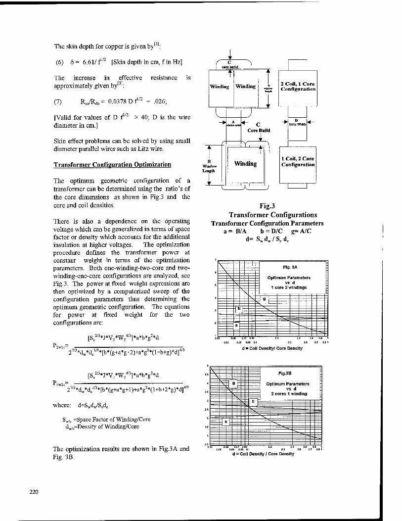
The skin depth for copper is given by' [3].
(6) 5= 6.61/f" [Skin depth in cm, fin Hz]
The increase in effective resistance is approximately given by :
(7) ■1/2
RJRäo = 0.0378 Df" + .026;
All [Valid for values of D f > 40; D is the wire diameter in cm.]
Skin effect problems can be solved by using small diameter parallel wires such as Litz wire.
Transformer Configuration Optimization
The optimum geometric configuration of a transformer can be determined using the ratio's of the core dimensions as shown in Fig. 3 and the
core and coil densities.
There is also a dependence on the operating voltage which can be generalized in terms of space factor or density which accounts for the additional insulation at higher voltages. The optimization procedure defines the transformer power at constant weight in terms of the optimization parameters. Both one-winding-two-core and two- winding-one-core configurations are analyzed, see Fig.3. The power at fixed weight expressions are then optimized by a computerized sweep of the configuration parameters thus determining the optimum geometric configuration. The equations for power at fixed weight for the two configurations are:
[S,273* J*VT*WT4/3] *a*b*g2*d
Mwl f~
r core build
t a.
Winding "Winding B wtadaw
2 Coil, 1 Core Configuration
V
I ) ->
Build
4
A wMewwMtl *- <
Core
D Strip Width ■*-
f Y, . \ a.
B Window Length
1 Winding
1 Coil, 2 Core Configuration
\ A J
Fig.3 Transformer Configurations
Transformer Configuration Parameters a = B/A b = D/C g= A/C
d= Sw dw / Sc dc JW "ff ' ^c "c
Fig. 3A
Optimum Parameters vs d
1 core 2 windings
9 ^_L_ A h L V 1 D r ^
V
2 a ^
0. 3 0.
0. 4
36
0.
0.
6
7
0.
0.
8
9
0 1
0 2
0
0
3
4
0
0
6
6
0
0
7
8
03 1
27/3*dw*dc1/3*[b*(g+a*g+2)+a*g2*(l+b+g)*d]4/3 d = Coil Density/ Core Density
[SCM*J*VT*WT
4/3] *a*b*g2*d *lw9rT"
27/3*dw*dc1/3*[b*(g+a*g+l)+a*g2*(l+b+2*g)*d]4/3
where: d=Swdw/Scdc
Sw/c =Space Factor of Winding/Core d^^Density of Winding/Core
The optimization results are shown in Fig. 3 A and Fig. 3B.
:
Optimum Parameters vs d
2 cores 1 winding
- 9
3 b t
1
d a b
0. 3 0.
0. A
£ 0.
0.C 6
7 0.
0. 8
9 0 1
0 2 0
0 z
4 0
0 s
6 0
0 7
8 1 0.9 1
d = Coil Density / Core Density
220
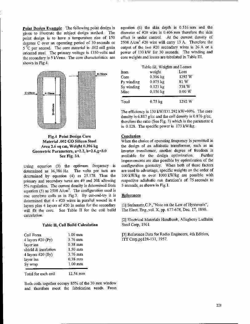
Point Design Example The following point design is given to illustrate the subject design method. The point design is to have a temperature rise of 150 degrees C over an operating period of 30 seconds or 5 °C per second. The core material is .002 mil grain oriented steel. The primary voltage is 1350 volts and the secondary is 5 kVrms. The core characteristics are shown in Fig.4.
4mm k '
gjjxl
C=10mm A=30mitt
111 E mm a
II
it. ■.
llillll w
D=26mm
equation (6) the skin depth is 0.516 mm and the diameter of #20 wire is 0.406 mm therefore the skin effect is under control. At the current density of 2508 A/cm2 #20 wire will carry 13 A. Therefore the output of the two #20 secondary wires is 26 A or a power of 130 kW for 30 seconds. The winding and core weights and losses are tabulated in Table III.
Table III, Weights and Losses Item weight Loss Core 0.396 kg 1292 W Py winding 0.075 kg 81 W Sy winding 0.123 kg 338 W Misc 0.156 kg 0.00 W
Total 0.75 kg 1292 W
The efficiency is 130 kW/131.292 kW=99%. The core density is 6.817 g/cc and the coil density is 0.876 g/cc, therefore the ratio (See Fig. 3) which is the parameter d is 0.128. The specific power is 173 kW/kg.
Fig.4 Point Design Core Material .002 GO Silicon Steel
Area 2.6 sq cm, Weight 0.396 kg Geometric Parameters, a=2.2, b=2.6,g=3.0
See Fig. 3A
Using equation (3) the optimum frequency is determined as 16,386 Hz. The volts per turn are determined by equation (4) as 25.178. Thus the primary and secondary turns are 49 and 208 allowing 5% regulation. The current density is determined from equation (5) as 2508 A/cm2. The configuration used is one core/two coils as in Fig.3. By cut-and-try it is determined that 4 - #20 wires in parallel wound in 4 layers plus 4 layers of #20 in series for the secondary will fit the core. See Table II for the coil build calculation.
Table n, Coil Build Calculation
Coil Form 1.00 mm 4 layers #20 (Py) 3.76 mm layer ins 0.38 mm shield & insulation 1.50 mm 4 layers #20 (Sy) 3.76 mm layer ins 0.38 mm Sy wrap 1.00 mm
Total for each coil 12.54 mm
Conclusion When the choice of operating frequency is permitted in the design of an adiabatic transformer, such as an inverter transformer, another degree of freedom is available for the design optimization. Further improvements are also possible by optimization of the configuration geometry. When both of these factors are used to advantage, specific weights on the order of lOOkW/kg to over 1000 kW/kg are possible with respective adiabatic run duration's of 75 seconds to 5 seconds, as shown in Fig.l.
References
[1] Steinmetz,C.P.,"Note on the Law of Hysteresis", The Elect. Eng.,vol. X, pp. 677-678, Dec. 17, 1890.
[2] Electrical Materials Handbook, Allegheny Ludlulm Steel Corp, 1961.
[3] Reference Data for Radio Engineers, 4th Edition, ITT Corp,ppl28-131, 1957.
Both coils together occupy 85% of the 30 mm window and therefore meet the fabrication needs. From
221
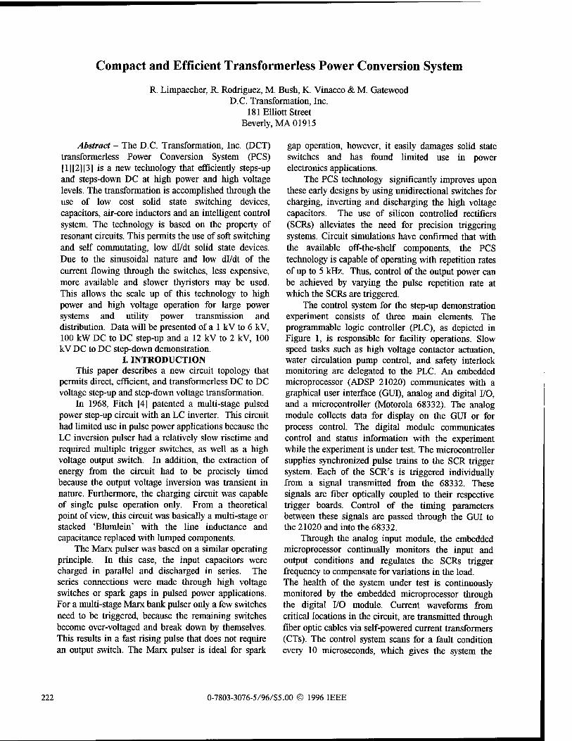
Compact and Efficient Transformerless Power Conversion System
R. Limpaecher, R. Rodriguez, M. Bush, K. Vinacco & M. Gatewood D.C. Transformation, Inc.
181 Elliott Street Beverly, MA 01915
Abstract - The D.C. Transformation, Inc. (DCT) transformerless Power Conversion System (PCS) [1][2][3] is a new technology that efficiently steps-up and steps-down DC at high power and high voltage levels. The transformation is accomplished through the use of low cost solid state switching devices, capacitors, air-core inductors and an intelligent control system. The technology is based on the property of resonant circuits. This permits the use of soft switching and self commutating, low dl/dt solid state devices. Due to the sinusoidal nature and low dl/dt of the current flowing through the switches, less expensive, more available and slower thyristors may be used. This allows the scale up of this technology to high power and high voltage operation for large power systems and utility power transmission and distribution. Data will be presented of a 1 kV to 6 kV, 100 kW DC to DC step-up and a 12 kV to 2 kV, 100 kV DC to DC step-down demonstration.
L INTRODUCTION This paper describes a new circuit topology that
permits direct, efficient, and transformerless DC to DC voltage step-up and step-down voltage transformation.
In 1968, Fitch [4] patented a multi-stage pulsed power step-up circuit with an LC inverter. This circuit had limited use in pulse power applications because the LC inversion pulser had a relatively slow risetime and required multiple trigger switches, as well as a high voltage output switch. In addition, the extraction of energy from the circuit had to be precisely timed because the output voltage inversion was transient in nature. Furthermore, the charging circuit was capable of single pulse operation only. From a theoretical point of view, this circuit was basically a multi-stage or stacked 'Blumlein' with the line inductance and capacitance replaced with lumped components.
The Marx pulser was based on a similar operating principle. In this case, the input capacitors were charged in parallel and discharged in series. The series connections were made through high voltage switches or spark gaps in pulsed power applications. For a multi-stage Marx bank pulser only a few switches need to be triggered, because the remaining switches become over-voltaged and break down by themselves. This results in a fast rising pulse that does not require an output switch. The Marx pulser is ideal for spark
gap operation, however, it easily damages solid state switches and has found limited use in power electronics applications.
The PCS technology significantly improves upon these early designs by using unidirectional switches for charging, inverting and discharging the high voltage capacitors. The use of silicon controlled rectifiers (SCRs) alleviates the need for precision triggering systems. Circuit simulations have confirmed that with the available off-the-shelf components, the PCS technology is capable of operating with repetition rates of up to 5 kHz. Thus, control of the output power can be achieved by varying the pulse repetition rate at which the SCRs are triggered.
The control system for the step-up demonstration experiment consists of three main elements. The programmable logic controller (PLC), as depicted in Figure 1, is responsible for facility operations. Slow speed tasks such as high voltage contactor actuation, water circulation pump control, and safety interlock monitoring are delegated to the PLC. An embedded microprocessor (ADSP 21020) communicates with a graphical user interface (GUI), analog and digital I/O, and a microcontroller (Motorola 68332). The analog module collects data for display on the GUI or for process control. The digital module communicates control and status information with the experiment while the experiment is under test. The microcontroller supplies synchronized pulse trains to the SCR trigger system. Each of the SCR's is triggered individually from a signal transmitted from the 68332. These signals are fiber optically coupled to their respective trigger boards. Control of the timing parameters between these signals are passed through the GUI to the 21020 and into the 68332.
Through the analog input module, the embedded microprocessor continually monitors the input and output conditions and regulates the SCRs trigger frequency to compensate for variations in the load. The health of the system under test is continuously monitored by the embedded microprocessor through the digital I/O module. Current waveforms from critical locations in the circuit, are transmitted through fiber optic cables via self-powered current transformers (CTs). The control system scans for a fault condition every 10 microseconds, which gives the system the
222 0-7803-3076-5/96/S5.00 © 1996 IEEE
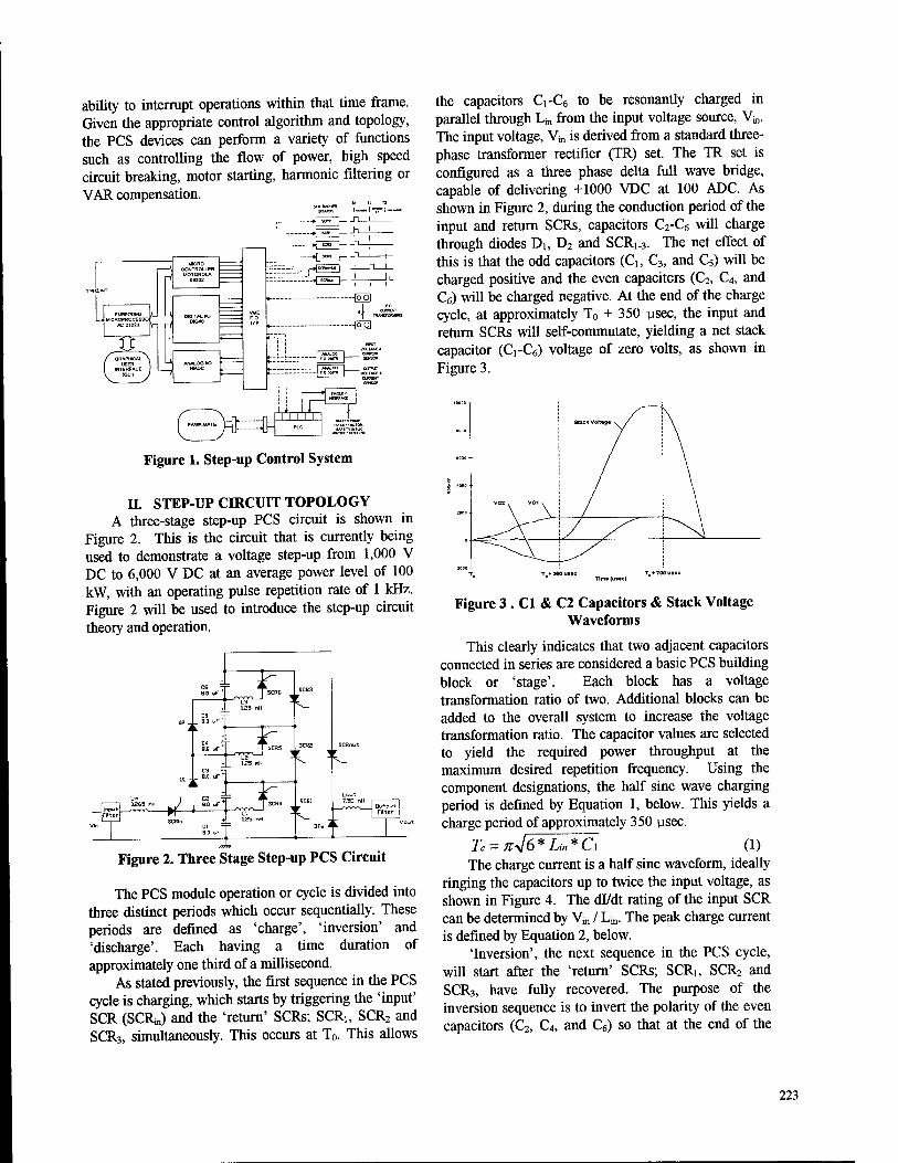
ability to interrupt operations within that time frame. Given the appropriate control algorithm and topology, the PCS devices can perform a variety of functions such as controlling the flow of power, high speed circuit breaking, motor starting, harmonic filtering or VAR compensation.
Figure 1. Step-up Control System
IL STEP-UP CIRCUIT TOPOLOGY A three-stage step-up PCS circuit is shown in
Figure 2. This is the circuit that is currently being used to demonstrate a voltage step-up from 1,000 V DC to 6,000 V DC at an average power level of 100 kW, with an operating pulse repetition rate of 1 kHz. Figure 2 will be used to introduce the step-up circuit theory and operation.
^~
SCR6 _,, i-vvv-i—I 5L
* TSCR5 J
^
^
Figure 2. Three Stage Step-up PCS Circuit
The PCS module operation or cycle is divided into three distinct periods which occur sequentially. These periods are defined as 'charge', 'inversion' and 'discharge'. Each having a time duration of approximately one third of a millisecond.
As stated previously, the first sequence in the PCS cycle is charging, which starts by triggering the 'input' SCR (SCR») and the 'return' SCRs; SCR, SCR2 and SCR3, simultaneously. This occurs at T0. This allows
the capacitors Ci-C6 to be resonantly charged in parallel through L^ from the input voltage source, Vj„. The input voltage, Vj„ is derived from a standard three- phase transformer rectifier (TR) set. The TR set is configured as a three phase delta full wave bridge, capable of delivering +1000 VDC at 100 ADC. As shown in Figure 2, during the conduction period of the input and return SCRs, capacitors C2-C6 will charge through diodes Di, D2 and SCRi_3. The net effect of this is that the odd capacitors (Ci, C3, and C5) will be charged positive and the even capacitors (Q>, C4, and C6) will be charged negative. At the end of the charge cycle, at approximately T0 + 350 usec, the input and return SCRs will self-commutate, yielding a net stack capacitor (Ci-C6) voltage of zero volts, as shown in Figure 3.
VC2 . VC1 .
Stack VoRaga * /
\ \ / y^ rM
T T.+ 3MUMC T. + 7 OOusac
Figure 3 . Cl & C2 Capacitors & Stack Voltage Waveforms
This clearly indicates that two adjacent capacitors connected in series are considered a basic PCS building block or 'stage'. Each block has a voltage transformation ratio of two. Additional blocks can be added to the overall system to increase the voltage transformation ratio. The capacitor values are selected to yield the required power throughput at the maximum desired repetition frequency. Using the component designations, the half sine wave charging period is defined by Equation 1, below. This yields a charge period of approximately 350 usec.
Tc = W6*Z»*Ci (1) The charge current is a half sine waveform, ideally
ringing the capacitors up to twice the input voltage, as shown in Figure 4. The dl/dt rating of the input SCR can be determined by Vjn / U,. The peak charge current is defined by Equation 2, below.
'Inversion', the next sequence in the PCS cycle, will start after the 'return' SCRs; SCR, SCR2 and SCR3, have fully recovered. The purpose of the inversion sequence is to invert the polarity of the even capacitors (C2, C4, and C6) so that at the end of the
223
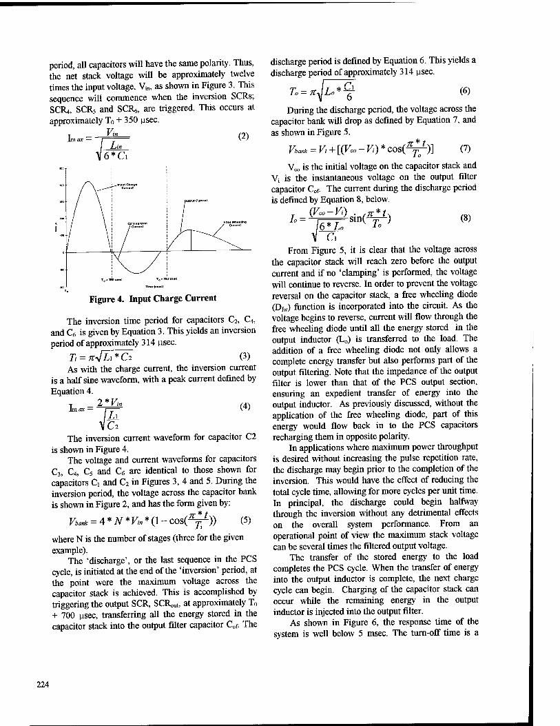
period, all capacitors will have the same polarity. Thus, the net stack voltage will be approximately twelve times the input voltage, V™ as shown in Figure 3. This sequence will commence when the inversion SCRs; SCR4, SCR5 and SCRs, are triggered. This occurs at approximately T0 + 350 ysec.
ViH— (2) liaax —
I 6*G
Figure 4. Input Charge Current
The inversion time period for capacitors C2, C4, and C6 is given by Equation 3. This yields an inversion period of approximately 314 ysec.
Ti = 7vjL\*Ci (3) As with the charge current, the inversion current
is a half sine waveform, with a peak current defined by Equation 4.
2* Vin lm<ax — (4)
The inversion current waveform for capacitor C2 is shown in Figure 4.
The voltage and current waveforms for capacitors C3, C4, C5 and C6 are identical to those shown for capacitors C, and C2 in Figures 3, 4 and 5. During the inversion period, the voltage across the capacitor bank is shown in Figure 2, and has the form given by:
7T*t^ Vbank = 4*N*Vin*(l- cos(^)) (5)
where N is the number of stages (three for the given example).
The 'discharge', or the last sequence in the PCS cycle, is initiated at the end of the 'inversion' period, at the point were the maximum voltage across the capacitor stack is achieved. This is accomplished by triggering the output SCR SCRout, at approximately T0
+ 700 usec, transferring all the energy stored in the capacitor stack into the output filter capacitor Cof. The
discharge period is defined by Equation 6. This yields a discharge period of approximately 314 usec.
To = 7cJi * C\ ' 6 (6)
During the discharge period, the voltage across the capacitor bank will drop as defined by Equation 7, and as shown in Figure 5.
Vbank = Vi+ [(Vco ~ Vi) * COSC^)] (7)
Vco is the initial voltage on the capacitor stack and Vi is the instantaneous voltage on the output filter capacitor Cof. The current during the discharge period is defined by Equation 8, below.
■ *t
") (8) /o=(fePsin(^ 1 6±U
Cx
To
From Figure 5, it is clear that the voltage across the capacitor stack will reach zero before the output current and if no 'clamping' is performed, the voltage will continue to reverse. In order to prevent the voltage reversal on the capacitor stack, a free wheeling diode (Dfw) function is incorporated into the circuit. As the voltage begins to reverse, current will flow through the free wheeling diode until all the energy stored in the output inductor (L0) is transferred to the load. The addition of a free wheeling diode not only allows a complete energy transfer but also performs part of the output filtering. Note that the impedance of the output filter is lower than that of the PCS output section, ensuring an expedient transfer of energy into the output inductor. As previously discussed, without the application of the free wheeling diode, part of this energy would flow back in to the PCS capacitors recharging them in opposite polarity.
In applications where maximum power throughput is desired without increasing the pulse repetition rate, the discharge may begin prior to the completion of the inversion. This would have the effect of reducing the total cycle time, allowing for more cycles per unit time. In principal, the discharge could begin halfway through the inversion without any detrimental effects on the overall system performance. From an operational point of view the maximum stack voltage can be several times the filtered output voltage.
The transfer of the stored energy to the load completes the PCS cycle. When the transfer of energy into the output inductor is complete, the next charge cycle can begin. Charging of the capacitor stack can occur while the remaining energy in the output inductor is injected into the output filter.
As shown in Figure 6, the response time of the system is well below 5 msec. The turn-off time is a
224
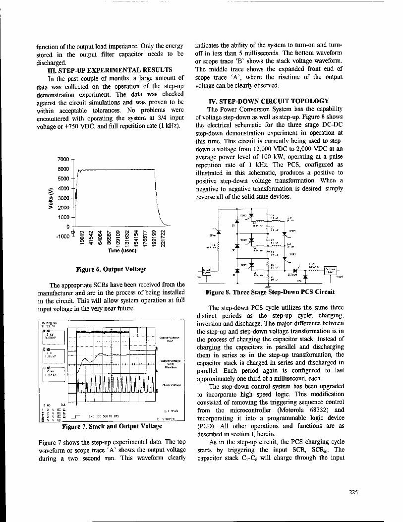
function of the output load impedance. Only the energy stored in the output filter capacitor needs to be discharged.
m. STEP-UP EXPERIMENTAL RESULTS In the past couple of months, a large amount of
data was collected on the operation of the step-up demonstration experiment. The data was checked against the circuit simulations and was proven to be within acceptable tolerances. No problems were encountered with operating the system at 3/4 input voltage or +750 VDC, and full repetition rate (1 kHz).
7000 T
6000
5000
-- 4000
« 3000
> 2000
1000
0
-1000
|W~
m (N Ti- r- O) (M ■*
■sr en m o C) m o in 9 (O S (O
■*
f- O)
(D r- . to g> n in s u
Time (usec)
Figure 6. Output Voltage
The appropriate SCRs have been received from the manufacturer and are in the process of being installed in the circuit. This will allow system operation at full input voltage in the very near future.
15-M3LJ-96 11:31:57
(»:H2 2 NS
3.08KV
I&H3- .? s i. ee w
I. M KV
; t
c
11 ll 11 ll1 1ft ftl II II Ift II I] III w [l II \\ lit If.
Oulput Voltage Vout
Rlsetjme
DC S, DC li, DC jh Ext DC 500PlV 1MJI
2.b MS/S
D STOPPED
Figure 7. Stack and Output Voltage
Figure 7 shows the step-up experimental data. The top waveform or scope trace 'A' shows the output voltage during a two second run. This waveform clearly
indicates the ability of the system to turn-on and turn- off in less than 5 milliseconds. The bottom waveform or scope trace 'B' shows the stack voltage waveform. The middle trace shows the expanded front end of scope trace 'A', where the risetime of the output voltage can be clearly observed.
IV. STEP-DOWN CIRCUIT TOPOLOGY The Power Conversion System has the capability
of voltage step-down as well as step-up. Figure 8 shows the electrical schematic for the three stage DC-DC step-down demonstration experiment in operation at this time. This circuit is currently being used to step- down a voltage from 12,000 VDC to 2,000 VDC at an average power level of 100 kW, operating at a pulse repetition rate of 1 kHz. The PCS, configured as illustrated in this schematic, produces a positive to positive step-down voltage transformation. When a negative to negative transformation is desired, simply reverse all of the solid state devices.
Figure 8. Three Stage Step-Down PCS Circuit
The step-down PCS cycle utilizes the same three distinct periods as the step-up cycle; charging, inversion and discharge. The major difference between the step-up and step-down voltage transformation is in the process of charging the capacitor stack. Instead of charging the capacitors in parallel and discharging them in series as in the step-up transformation, the capacitor stack is charged in series and discharged in parallel. Each period again is configured to last approximately one third of a millisecond, each.
The step-down control system has been upgraded to incorporate high speed logic. This modification consisted of removing the triggering sequence control from the microcontroller (Motorola 68332) and incorporating it into a programmable logic device (PLD). All other operations and functions are as described in section I, herein.
As in the step-up circuit, the PCS charging cycle starts by triggering the input SCR, SCRin. The capacitor stack Ci-C6 will charge through the input
225
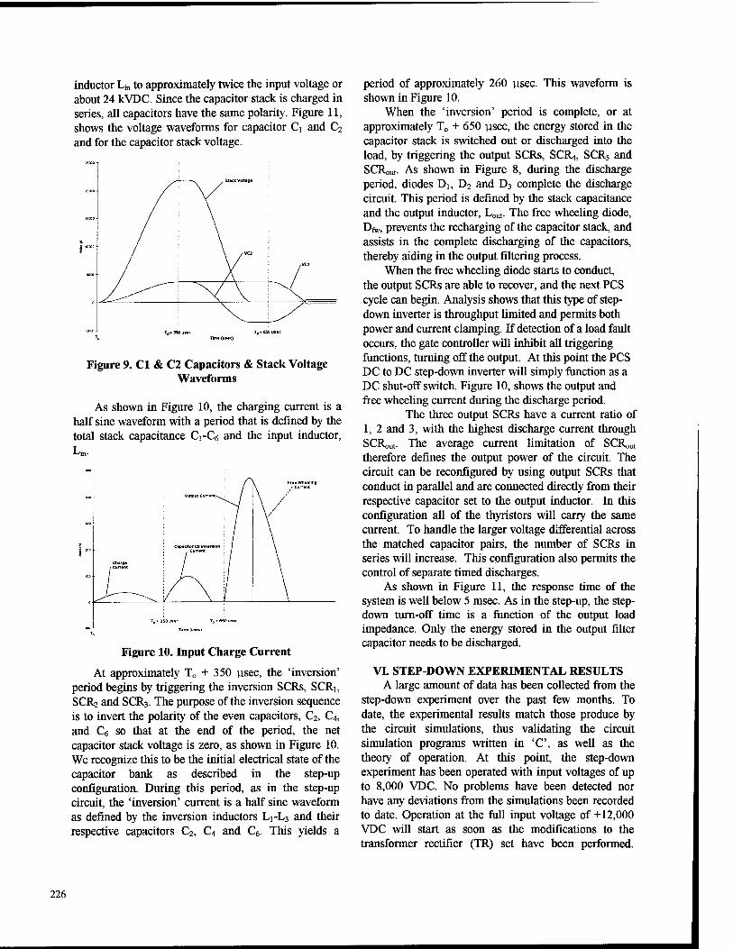
inductor Lh, to approximately twice the input voltage or about 24 kVDC. Since the capacitor stack is charged in series, all capacitors have the same polarity. Figure 11, shows the voltage waveforms for capacitor d and C2
and for the capacitor stack voltage.
Figure 9. Cl & C2 Capacitors & Stack Voltage Waveforms
As shown in Figure 10, the charging current is a half sine waveform with a period that is defined by the total stack capacitance Ci-C6 and the input inductor,
Ft«* Wheeling
Figure 10. Input Charge Current
At approximately TD + 350 ysec, the 'inversion' period begins by triggering the inversion SCRs, SCRi, SCR2 and SCR3. The purpose of the inversion sequence is to invert the polarity of the even capacitors, C2, C4, and C6 so that at the end of the period, the net capacitor stack voltage is zero, as shown in Figure 10. We recognize this to be the initial electrical state of the capacitor bank as described in the step-up configuration. During this period, as in the step-up circuit, the 'inversion' current is a half sine waveform as defined by the inversion inductors L1-L3 and their respective capacitors C2, C4 and C6. This yields a
period of approximately 260 usec. This waveform is shown in Figure 10.
When the 'inversion' period is complete, or at approximately T0 + 650 ysec, the energy stored in the capacitor stack is switched out or discharged into the load, by triggering the output SCRs, SCR,, SCR5 and SCRout. As shown in Figure 8, during the discharge period, diodes D], D2 and D3 complete the discharge circuit. This period is defined by the stack capacitance and the output inductor, Lout. The free wheeling diode, Dfw, prevents the recharging of the capacitor stack, and assists in the complete discharging of the capacitors, thereby aiding in the output filtering process.
When the free wheeling diode starts to conduct, the output SCRs are able to recover, and the next PCS cycle can begin. Analysis shows that this type of step- down inverter is throughput limited and permits both power and current clamping. If detection of a load fault occurs, the gate controller will inhibit all triggering functions, turning off the output. At this point the PCS DC to DC step-down inverter will simply function as a DC shut-off switch. Figure 10, shows the output and free wheeling current during the discharge period.
The three output SCRs have a current ratio of 1, 2 and 3, with the highest discharge current through SCRout. The average current limitation of SCRoUt
therefore defines the output power of the circuit. The circuit can be reconfigured by using output SCRs that conduct in parallel and are connected directly from their respective capacitor set to the output inductor. In this configuration all of the thyristors will carry the same current. To handle the larger voltage differential across the matched capacitor pairs, the number of SCRs in series will increase. This configuration also permits the control of separate timed discharges.
As shown in Figure 11, the response time of the system is well below 5 msec. As in the step-up, the step- down turn-off time is a function of the output load impedance. Only the energy stored in the output filter capacitor needs to be discharged.
VL STEP-DOWN EXPERIMENTAL RESULTS A large amount of data has been collected from the
step-down experiment over the past few months. To date, the experimental results match those produce by the circuit simulations, thus validating the circuit simulation programs written in 'C, as well as the theory of operation. At this point, the step-down experiment has been operated with input voltages of up to 8,000 VDC. No problems have been detected nor have any deviations from the simulations been recorded to date. Operation at the full input voltage of +12,000 VDC will start as soon as the modifications to the transformer rectifier (TR) set have been performed.
226
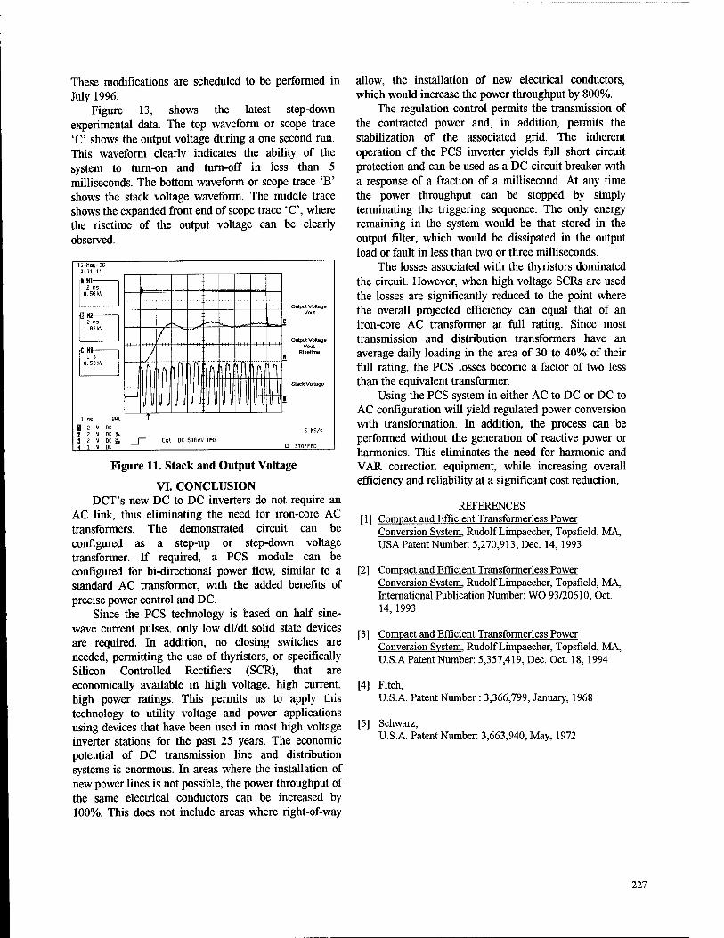
These modifications are scheduled to be performed in My 1996.
Figure 13, shows the latest step-down experimental data. The top waveform or scope trace 'C shows the output voltage during a one second run. This waveform clearly indicates the ability of the system to turn-on and turn-off in less than 5 milliseconds. The bottom waveform or scope trace 'B' shows the stack voltage waveform. The middle trace shows the expanded front end of scope trace 'C, where the risetime of the output voltage can be clearly observed.
Output Voltage Vout.
Rise Üme
Stack Voltage
Figure 11. Stack and Output Voltage
VI. CONCLUSION DCT's new DC to DC inverters do not require an
AC link, thus eliminating the need for iron-core AC transformers. The demonstrated circuit can be configured as a step-up or step-down voltage transformer. If required, a PCS module can be configured for bi-directional power flow, similar to a standard AC transformer, with the added benefits of precise power control and DC.
Since the PCS technology is based on half sine- wave current pulses, only low dl/dt solid state devices are required. In addition, no closing switches are needed, permitting the use of thyristors, or specifically Silicon Controlled Rectifiers (SCR), that are economically available in high voltage, high current, high power ratings. This permits us to apply this technology to utility voltage and power applications using devices that have been used in most high voltage inverter stations for the past 25 years. The economic potential of DC transmission line and distribution systems is enormous. In areas where the installation of new power lines is not possible, the power throughput of the same electrical conductors can be increased by 100%. This does not include areas where right-of-way
allow, the installation of new electrical conductors, which would increase the power throughput by 800%.
The regulation control permits the transmission of the contracted power and, in addition, permits the stabilization of the associated grid. The inherent operation of the PCS inverter yields full short circuit protection and can be used as a DC circuit breaker with a response of a fraction of a millisecond. At any time the power throughput can be stopped by simply terminating the triggering sequence. The only energy remaining in the system would be that stored in the output filter, which would be dissipated in the output load or fault in less than two or three milliseconds.
The losses associated with the thyristors dominated the circuit. However, when high voltage SCRs are used the losses are significantly reduced to the point where the overall projected efficiency can equal that of an iron-core AC transformer at full rating. Since most transmission and distribution transformers have an average daily loading in the area of 30 to 40% of their full rating, the PCS losses become a factor of two less than the equivalent transformer.
Using the PCS system in either AC to DC or DC to AC configuration will yield regulated power conversion with transformation. In addition, the process can be performed without the generation of reactive power or harmonics. This eliminates the need for harmonic and VAR correction equipment, while increasing overall efficiency and reliability at a significant cost reduction.
REFERENCES [1] Compact and Efficient Transformerless Power
Conversion System. Rudolf Limpaecher, Topsfield, MA, USA Patent Number: 5,270,913, Dec. 14, 1993
[2] Compact and Efficient Transformerless Power Conversion System, Rudolf Limpaecher, Topsfield, MA, International Publication Number: WO 93/20610, Oct. 14, 1993
[3] Compact and Efficient Transformerless Power Conversion System. Rudolf Limpaecher, Topsfield, MA, USA Patent Number: 5,357,419, Dec. Oct. 18, 1994
[4] Fitch, U.S.A. Patent Number : 3,366,799, January, 1968
[5] Schwarz, U.S.A. Patent Number: 3,663,940, May, 1972
227
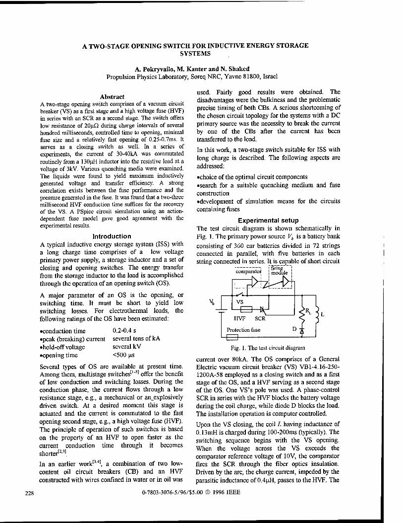
A TWO-STAGE OPENING SWITCH FOR INDUCTIVE ENERGY STORAGE SYSTEMS
A. Pokryvailo, M. Kanter and N. Snaked Propulsion Physics Laboratory, Soreq NRC, Yavne 81800, Israel
Abstract A two-stage opening switch comprises of a vacuum circuit breaker (VS) as a first stage and a high voltage fuse (HVF) in series with an SCR as a second stage. The switch offers low resistance of 20uQ during charge intervals of several hundred milliseconds, controlled time to opening, minimal fuse size and a relatively fast opening of 0.25-0.7ms. It serves as a closing switch as well. In a series of experiments, the current of 30-40kA was commutated routinely from a 130uH inductor into the resistive load at a voltage of 3kV. Various quenching media were examined. The liquids were found to yield maximum inductively generated voltage and transfer efficiency. A strong correlation exists between the fuse performance and the pressure generated in the fuse. It was found that a two-three millisecond HVF conduction time suffices for the recovery of the VS. A PSpice circuit simulation using an action- dependent fuse model gave good agreement with the experimental results.
Introduction A typical inductive energy storage system (ISS) with a long charge time comprises of a low voltage primary power supply, a storage inductor and a set of closing and opening switches. The energy transfer from the storage inductor to the load is accomplished through the operation of an opening switch (OS).
A major parameter of an OS is the opening, or switching time. It must be short to yield low switching losses. For electrothermal loads, the following ratings of the OS have been estimated:
•conduction time •peak (breaking) current •hold-off voltage •opening time
0.2-0.4 s several tens of kA several kV <500 ias
Several types of OS are available at present time. Among them, multistage switches11"31 offer the benefit of low conduction and switching losses. During the conduction phase, the current flows through a low resistance stage, e.g., a mechanical or an_explosively driven switch. At a desired moment this stage is actuated and the current is commutated to the fast opening second stage, e.g., a high voltage fuse (HVF). The principle of operation of such switches is based on the property of an HVF to open faster as the current conduction time through it becomes shorter'2'31.
In an earlier work13'41, a combination of two low- content oil circuit breakers (CB) and an HVF constructed with wires confined in water or in oil was
used. Fairly good results were obtained. The disadvantages were the bulkiness and the problematic precise timing of both CBs. A serious shortcoming of the chosen circuit topology for the systems with a DC primary source was the necessity to break the current by one of the CBs after the current has been transferred to the load.
In this work, a two-stage switch suitable for ISS with long charge is described. The following aspects are addressed:
•choice of the optimal circuit components •search for a suitable quenching medium and fuse construction •development of simulation means for the circuits containing fuses
Experimental setup The test circuit diagram is shown schematically in Fig. 1. The primary power source Vb is a battery bank consisting of 360 car batteries divided in 72 strings connected in parallel, with five batteries in each string connected in series. It is capable of short circuit
i comparator! ! module
Protection fuse
Fig. 1. The test circuit diagram
current over 80kA. The OS comprises of a General Electric vacuum circuit breaker (VS) VB1-4.16-250- 1200A-58 employed as a closing switch and as a first stage of the OS, and a HVF serving as a second stage of the OS. One VS's pole was used. A phase-control SCR in series with the HVF blocks the battery voltage during the coil charge, while diode D blocks the load. The installation operation is computer controlled.
Upon the VS closing, the coil L having inductance of 0.13mH is charged during 100-200ms (typically). The switching sequence begins with the VS opening. When the voltage across the VS exceeds the comparator reference voltage of 10V, the comparator fires the SCR through the fiber optics insulation. Driven by the arc, the charge current, impeded by the parasitic inductance of 0.4(iH, passes to the HVF. The
228 0-7803-3076-5/96/S5.00 © 1996 IEEE

HVF conduction lasts typically 2-3 milliseconds to enable the recovery of the VS dielectric strength. Upon the HVF blowing, the opening sequence is accomplished by the current transfer to a resistive load. The coil, diagnostic means and the data evaluation methods are described in[5].
The choice of the circuit components and topology was guided by the following considerations:
1. The vacuum insulation recovers after the current interruption much faster than any other kind of insulation.
2. The voltage across short vacuum arcs is not less than 15 V. Therefore, if the voltage across the VS contacts is lower, the arc will be extinct. This voltage is
V^=Vf+Vscr (1) where Vf- is the voltage across the fuse and Vscr -the voltage drop on the SCR. The latter is not more than 5V for large commercial SCR's. Thus, if Vf is less than 8-9V, the arc extinction is guaranteed. This imposes a strict limitation on the HVF initial resistance and certainly is a shortcoming in comparison to CB's of other types, having typically a much higher arc voltage. 3. Using the SCR as a closing switch allows for precise timing. Thus the fuse conduction time can be decreased to a possible minimum along with an OS mass and size reduction.
4. The VS in the chosen topology serves both as a CS and an OS.
HVF construction One of the hermetic fuse housings is shown in Fig. 2. It comprises of a glass fiber reinforced epoxy
5-
Fig. 2. Fuse housing
cylinder 1 placed between steel flanges 2. A number of copper fuse links, or strips, 3 having equally spaced slots are placed between flanges 2 and contact brass boards 4. The construction is tightened by screws (not shown). A pressure transducer 5, model 118A of PCB Piezotronics, is incorporated into the board 4 through an insulating insert. To ensure the safe operation, a rupture disk 6 is installed in the other board. It opens when the pressure exceeds
300bar. An elastic rubber shock absorber of 20- 40cm3 is placed inside the housing. The volume of the latter is 200cm3. O-ring seals enable the use of liquid quenching media.
Similar smaller housings, with a volume of 20- 50cm3 and a shock absorber of 5-20cm3 were also employed. The small size allowed for higher pressure of 700bar. In these housings, besides strips, a number of copper wires with a cross-section of 1.5mm2, 30mm long were used. The HVF initial resistance was sufficiently small, satisfying thus Eq. 1 to ensure the arc extinction.
Experimental results About 90 experiments, with a wide variety of the parameters were performed. The charge time varied from 35ms to 230ms, which corresponded to the breaking current of 9-40kA. However, the HVF conduction time was pinned to about 2-3ms to ensure the VS recovery, although is had been found that 0.5ms also suffices for this purpose. The strip parameters were varied as well. Several quenching mediums were tried, including silica and magnesia powders, solid fillings (paraffin, silicon compounds) and liquid fillings. Among them, a 95% distilled water+5% glycerol solution (DWG), silicon oil and transformer oil were found to yield a better performance. The test results for several typical experiments are summarized in table 1. For convenience, the list of symbols is provided below.
Nomenclature
lbr - breaking current
^sw ' switching time
T - HVF conduction time C
Vswm - HVF peak voltage
Pm - peak fuse pressure Em - peak inductively generated field in HVF NM - not measured
Table 1. Test results
No hr 7c T V swm Pm housing
kA ms ms kV bar kV/cm
l*s 30 2.4 0.5 2.3 NM 12 small
2"s 37.3 5 1.1 2.4 250 3.0 large
3*s 30.5 3 0.6 2.3 200 5.8 large 4*s 38 3.5 0.7 2.9 NM 3.6 large c*w 9 3 0.35 3.5 450 1 small
6iw 28.3 2 0.25 2.5 NM 0.8 small
■oil, ■ DWG solution, s - strips, w - wires
The wave forms obtained in experiment No. 3 are shown in Fig. 3-4. It is seen that after the contacts' opening, the arc drives the current to the HVF. Since the arc voltage is about 20V, it must be in a diffuse mode[6]. Such arcs do not damage the contacts considerably. The HVF conducts the full charge current for 2.2ms and blows out, transferring the
229
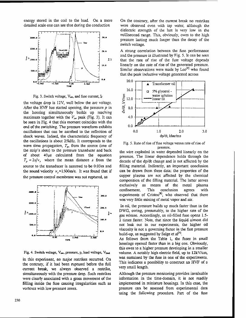
energy stored in the coil to the load. On a more detailed scale one can see that during the conduction
Fig. 3. Switch voltage, V„,, and fuse current, If
the voltage drop is 12V, well below the arc voltage. After the HVF has started opening, the pressure p in the housing simultaneously builds up reaching maximum together with the V„ peak (Fig. 3). It can be seen in Fig. 4 that this moment coincides with the end of the switching. The pressure waveform exhibits oscillations that can be ascribed to the reflection of shock waves. Indeed, the characteristic frequency of the oscillations is about 25kHz. It corresponds to the wave time propagation, Tp, from the source (one of the strip's slots) to the pressure transducer and back of about 40us calculated from the equation T = 2s/vs where the mean distance s from the
source to the transducer is assumed to be 0.03m and the sound velocity vJ=1500m/s. It was found that if
the pressure control membrane was not ruptured, as
Fig. 4. Switch voltage, V„, pressure, p, load voltage, Vio«d
in this experiment, no major restrikes occurred. On the contrary, if it had been ruptured before the full current break, we always observed a restrike, simultaneously with the pressure drop. Such restrikes were clearly associated with a gross movement of the filling inside the fuse causing irregularities such as vortexes with low pressure zones.
On the contrary, after the current break no restrikes were observed even with tap water, although the dielectric strength of the last is very low in the millisecond range. This, obviously, owes to the high pressure lasting much longer than the decay of the switch voltage.
A strong correlation between the fuse performance and the pressure is illustrated by Fig. 5. It can be seen that the rate of rise of the fuse voltage depends linearly on the rate of rise of the generated pressure. Similar observations were made by Lee191 who found that the peak inductive voltage generated across
20.0
16.0
12.0
5 8.0 >
4.0
0.0
A Transformer oil
-A. □ 5% glycerol - water solution
linear fit .s /
j/k.
0.0 1.0 2.0 dp/dt, kbar/ms
3.0
Fig. 5. Rate of rise of fuse voltage versus rate of rise of pressure,
the wire exploded in water depended linearly on the pressure. The linear dependence holds through the decade of the dp/dt change and is not affected by the filling material. Indirectly, an important conclusion can be drawn from these data: the properties of the copper plasma are not affected by the chemical composition of the filling material. The latter serves exclusively as means of the metal plasma confinement. This conclusion agrees with experiments of Cristou18', who observed that there was very little mixing of metal vapor and air.
In oil, the pressure builds up much faster than in the DWG, owing, presumably, to the higher rate of the gas release. Accordingly, an oil-filled fuse opens 1.5- 2 times faster. Note, that since the liquid almost did not leak out in our experiments, the higher oil viscosity is not a governing factor in the fast pressure build-up, as suggested by Salge et al[4!. As follows from the Table 1, the fuses in small housings opened faster than in a big one. Obviously, this owes to a higher pressure developing in a smaller volume. A notably high electric field, up to 12kV/cm, was sustained by the fuse in one of the experiments. This indicates a possibility to construct an UVF of a very small length.
Although the pressure monitoring provides invaluable information in the time-domain, it is not readily implemented in miniature housings. In this case, the pressure can be assessed from experimental data using the following procedure. Part of the fuse
230
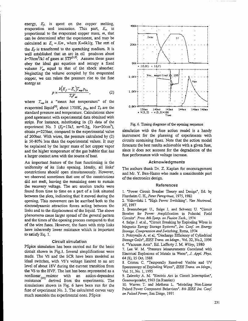
energy, Ej, is spent on the copper melting, evaporation and ionization. This part, £„ is proportional to the evaporated copper mass, m, that can be determined after the experiment, and may be calculated as Ec = Km, where K»6kJ/g. The rest of
the Ef is transferred to the quenching medium. It is well established that an arc in oil produces about Jfc=70cm3/kJ of gases at STP11,91. Assume these gases obey the ideal gas equation and occupy a fixed volume Vsa equal to that of the shock absorber. Neglecting the volume occupied by the evaporated copper, we can relate the pressure rise to the fuse energy as
k{Ef-Ec)T«yP<>a T0V„
(2)
where T is a "mean hot temperature" of the
evaporated liquid[9), about 1700K, poa and T0 are the standard pressure and temperature. Calculations show good agreement with experimental data obtained with strips. For instance, substituting in (2) data of the experiment No. 3 (£^=13kJ, m=0.2g, Vsa=20cm3), obtain p=223bar, compared to the experimental value of 200bar. With wires, the pressure calculated by (2) is 50-80% less than the experimental values. It may be explained by the larger mass of hot copper vapor and the higher temperature of the gas bubble that has a larger contact area with the source of heat.
An important feature of the fuse functioning is the uniformity of its links opening. Ideally, all links' constrictions should open simultaneously. However, we observed sometimes that one of the constrictions did not melt, leaving the remaining ones to sustain the recovery voltage. The arc erosion tracks were found from time to time on a part of a link situated between the slots, indicating that it moved during the opening. This movement can be ascribed both to the electrodynamic attraction forces acting between the links and to the displacement of the liquid. The above phenomena cause larger spread of the general pattern and the times of the opening process compared to that of the wire fuses. However, the fuses with strip links have inherently lower resistance which is important to satisfy Eq. 1.
Circuit simulation PSpice simulation has been carried out for the basic circuit shown in Fig.l. Several simplifications were made. The VS and the SCR have been modeled as ideal switches, with VS's voltage limited to an arc level of about 18V during the current transition from the VS to the HVF. The last has been represented as a nonlinear resistor with an action-dependent resistance derived from the experiments. The simulations shown in Fig. 6 have been run for the fuse of experiment No. 3. The calculated curves very much resemble the experimental ones. PSpice
40KA + h 1— -
20KA
OKflH ^
2.0KV+ •
1.0KV +
O.OKV-fS 13S015 HOms 142ms
• V(3,5) • v(3,S)«100 Time
144ms 146ns 146ms
Fig. 6. Timing diagrams of the opening sequence
simulation with the fuse action model is a handy instrument for the planning of experiments with circuits containing fuses. Note that the action model forecasts the best results achievable with a given fuse, since it does not account for the degradation of the fuse performance with voltage increase.
Acknowledgments
The authors thank Dr. Z. Kaplan for encouragement and Mr. Y. Ben-Hamo who made a considerable part of the electronics design.
References
1. "Power Circuit Breaker Theory and Design", Ed by Flurcheim C. H., Peter Peregrinus, 1975,1982 2. Vitkovitski I. "High Power Switching". Van Nostrand, NY, 1987 3. Braunsberger U., Salge J. and Schwarz U. "Circuit Breaker for Power Amplification in Poloidal Field Circuits". Proc. 8th Symp. on Fusion Tech., 1974 4. Salge J. etaL, "Circuit Breaking by Exploding Wires in Magnetic Energy Storage Systems", Int. Conf. on Energy Storage, Compression and Switching, Roma, 1974 5. Pokryvailo A. et al, "Discharge Efficiency of Cylindrical Storage Coils", IEEE Trans, on Magn., Vol. 32, No.2,1996 6. "Vacuum Arcs". Ed. Lafferry J. M. Wiley, 1980 7. Lee W. M. "Pressure Measurements Correlated with Electrical Explosions of Metals in Water", J. Appl. Phys. 64(8), 15 0ct 1988 8. Cristou C. 'Temporally Resolved Visible and UV Spectroscopy of Exploding Wires", IEEE Trans, on Magn., Vol. 31, No. 1,1995 9. Zalessky A. M. "Electric Arc in Circuit Interruption", Gosenergoizdat, 1963 (in Russian) 10. Warren T. and Matheus L. "Modeling Non-Linear Pulsed Power Component Behaviors". 8th IEEE Int. Conf. on Pulsed Power, San Diego, 1991
231
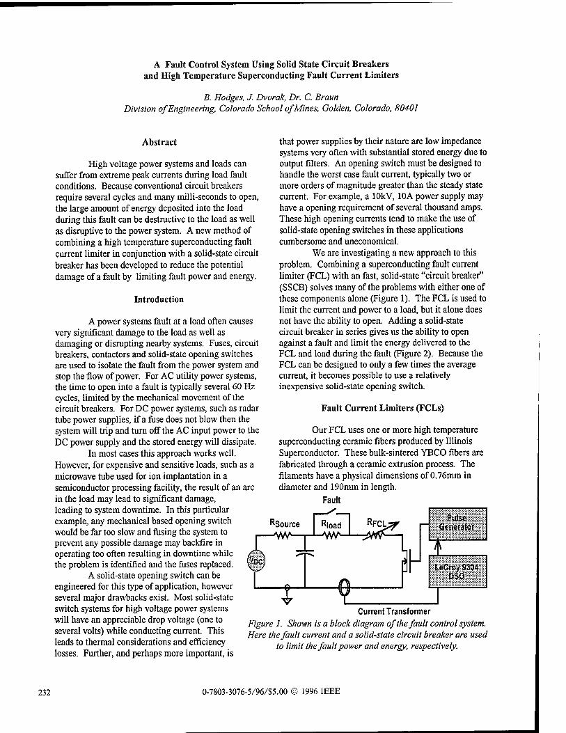
A Fault Control System Using Solid State Circuit Breakers and High Temperature Superconducting Fault Current Limiters
B. Hodges, J. Dvorak, Dr. C. Braun Division of Engineering, Colorado School of Mines, Golden, Colorado, 80401
Abstract
High voltage power systems and loads can suffer from extreme peak currents during load fault conditions. Because conventional circuit breakers require several cycles and many milli-seconds to open, the large amount of energy deposited into the load during this fault can be destructive to the load as well as disruptive to the power system. A new method of combining a high temperature superconducting fault current limiter in conjunction with a solid-state circuit breaker has been developed to reduce the potential damage of a fault by limiting fault power and energy.
Introduction
A power systems fault at a load often causes very significant damage to the load as well as damaging or disrupting nearby systems. Fuses, circuit breakers, contactors and solid-state opening switches are used to isolate the fault from the power system and stop the flow of power. For AC utility power systems, the time to open into a fault is typically several 60 Hz cycles, limited by the mechanical movement of the circuit breakers. For DC power systems, such as radar tube power supplies, if a fuse does not blow then the system will trip and turn off the AC input power to the DC power supply and the stored energy will dissipate.
In most cases this approach works well. However, for expensive and sensitive loads, such as a microwave tube used for ion implantation in a semiconductor processing facility, the result of an arc in the load may lead to significant damage, leading to system downtime. In this particular example, any mechanical based opening switch would be far too slow and fusing the system to prevent any possible damage may backfire in operating too often resulting in downtime while the problem is identified and the fuses replaced.
A solid-state opening switch can be engineered for this type of application, however several major drawbacks exist. Most solid-state switch systems for high voltage power systems will have an appreciable drop voltage (one to several volts) while conducting current. This leads to thermal considerations and efficiency losses. Further, and perhaps more important, is
that power supplies by their nature are low impedance systems very often with substantial stored energy due to output filters. An opening switch must be designed to handle the worst case fault current, typically two or more orders of magnitude greater than the steady state current. For example, a lOkV, 10A power supply may have a opening requirement of several thousand amps. These high opening currents tend to make the use of solid-state opening switches in these applications cumbersome and uneconomical.
We are investigating a new approach to this problem. Combining a superconducting fault current limiter (FCL) with an fast, solid-state "circuit breaker" (SSCB) solves many of the problems with either one of these components alone (Figure 1). The FCL is used to limit the current and power to a load, but it alone does not have the ability to open. Adding a solid-state circuit breaker in series gives us the ability to open against a fault and limit the energy delivered to the FCL and load during the fault (Figure 2). Because the FCL can be designed to only a few times the average current, it becomes possible to use a relatively inexpensive solid-state opening switch.
Fault Current Limiters (FCLs)
Our FCL uses one or more high temperature superconducting ceramic fibers produced by Illinois Superconductor. These bulk-sintered YBCO fibers are fabricated through a ceramic extrusion process. The filaments have a physical dimensions of 0.76mm in diameter and 190mm in length.
Fault
Pulse Generator
LeCroy 9304 D$0
Current Transformer Figure 1. Shown is a block diagram of the fault control system. Here the fault current and a solid-state circuit breaker are used
to limit the fault power and energy, respectively.
232 0-7803-3076-5/96/S5.00 © 1996 IEEE
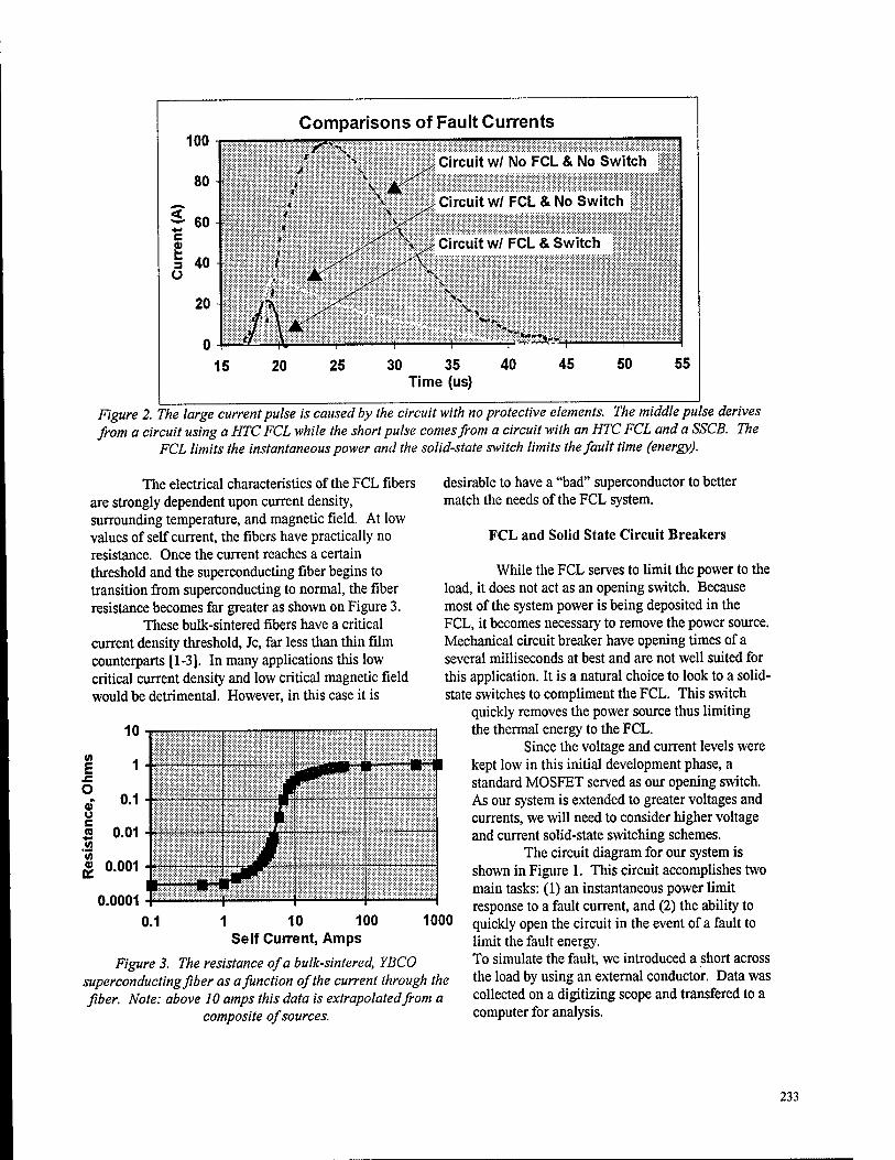
100-I
80
§60 c 8» 3 40 ü
20
0 1
Comparisons of Fault Currents
5
/~-v * "*> , Circuit w/ No FCL & No Switch
* \ /^ ■ ■ i \*r
- ' t \ s Circuit w/ FCL & No Switch
%.. ■ • >>r * • / \x Circuit w/ FCL & Switch
5 20 25 30 35 40 45 50 5 Time (us)
Figure 2. The large current pulse is caused by the circuit with no protective elements. The middle pulse derives from a circuit using a HTC FCL while the short pulse comes from a circuit with an HTC FCL and a SSCB. The
FCL limits the instantaneous power and the solid-state switch limits the fault time (energy).
The electrical characteristics of the FCL fibers are strongly dependent upon current density, surrounding temperature, and magnetic field. At low values of self current, the fibers have practically no resistance. Once the current reaches a certain threshold and the superconducting fiber begins to transition from superconducting to normal, the fiber resistance becomes far greater as shown on Figure 3.
These bulk-sintered fibers have a critical current density threshold, Jc, far less than thin film counterparts [1-3]. In many applications this low critical current density and low critical magnetic field would be detrimental. However, in this case it is
tfl E
10
0.1 -1 01 u J 0.01 in
0.001
0.0001
i flW '
I J !!=^ r
0.1 1 10 100 1000 Self Current, Amps
Figure 3. The resistance of a bulk-sintered, YBCO superconducting fiber as a function of the current through the fiber. Note: above 10 amps this data is extrapolated from a
composite of sources.
desirable to have a "bad" superconductor to better match the needs of the FCL system.
FCL and Solid State Circuit Breakers
While the FCL serves to limit the power to the load, it does not act as an opening switch. Because most of the system power is being deposited in the FCL, it becomes necessary to remove the power source. Mechanical circuit breaker have opening times of a several milliseconds at best and are not well suited for this application. It is a natural choice to look to a solid- state switches to compliment the FCL. This switch
quickly removes the power source thus limiting the thermal energy to the FCL.
Since the voltage and current levels were kept low in this initial development phase, a standard MOSFET served as our opening switch. As our system is extended to greater voltages and currents, we will need to consider higher voltage and current solid-state switching schemes.
The circuit diagram for our system is shown in Figure 1. This circuit accomplishes two main tasks: (1) an instantaneous power limit response to a fault current, and (2) the ability to quickly open the circuit in the event of a fault to limit the fault energy. To simulate the fault, we introduced a short across the load by using an external conductor. Data was collected on a digitizing scope and transfered to a computer for analysis.
233
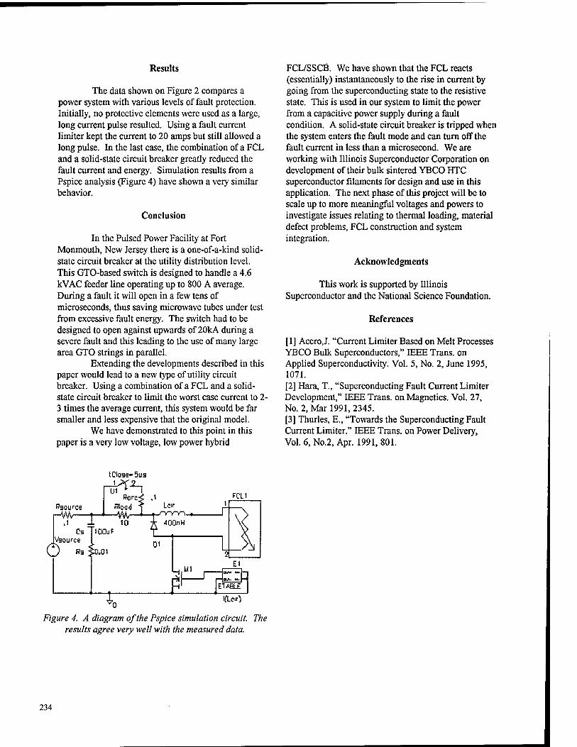
Results
The data shown on Figure 2 compares a power system with various levels of fault protection. Initially, no protective elements were used as a large, long current pulse resulted. Using a fault current limiter kept the current to 20 amps but still allowed a long pulse. In the last case, the combination of a FCL and a solid-state circuit breaker greatly reduced the fault current and energy. Simulation results from a Pspice analysis (Figure 4) have shown a very similar behavior.
Conclusion
In the Pulsed Power Facility at Fort Monmouth, New Jersey there is a one-of-a-kind solid- state circuit breaker at the utility distribution level. This GTO-based switch is designed to handle a 4.6 kVAC feeder line operating up to 800 A average. During a fault it will open in a few tens of microseconds, thus saving microwave tubes under test from excessive fault energy. The switch had to be designed to open against upwards of 20kA during a severe fault and this leading to the use of many large area GTO strings in parallel.
Extending the developments described in this paper would lead to a new type of utility circuit breaker. Using a combination of a FCL and a solid- state circuit breaker to limit the worst case current to 2- 3 times the average current, this system would be far smaller and less expensive that the original model.
We have demonstrated to this point in this paper is a very low voltage, low power hybrid
FCL/SSCB. We have shown that the FCL reacts (essentially) instantaneously to the rise in current by going from the superconducting state to the resistive state. This is used in our system to limit the power from a capacitive power supply during a fault condition. A solid-state circuit breaker is tripped when the system enters the fault mode and can turn off the fault current in less than a microsecond. We are working with Illinois Superconductor Corporation on development of their bulk sintered YBCO HTC superconductor filaments for design and use in this application. The next phase of this project will be to scale up to more meaningful voltages and powers to investigate issues relating to thermal loading, material defect problems, FCL construction and system integration.
Acknowledgments
This work is supported by Illinois Superconductor and the National Science Foundation.
References
[1] Acero,J. "Current Limiter Based on Melt Processes YBCO Bulk Superconductors," IEEE Trans, on Applied Superconductivity. Vol. 5, No. 2, June 1995, 1071. [2] Hara, T., "Superconducting Fault Current Limiter Development," IEEE Trans, on Magnetics. Vol. 27, No. 2, Mar 1991, 2345. [3] Thurles, E., "Towards the Superconducting Fault Current Limiter." IEEE Trans, on Power Delivery, Vol. 6, No.2, Apr. 1991, 801.
(Close-5u 3
Rsource HM 1—*■
1 J. Cs T'OOuF
Source
Bgrc< .1 Blöfld T Lcir
10
FCU
Figure 4. A diagram of the Pspice simulation circuit. The results agree very well with the measured data.
234
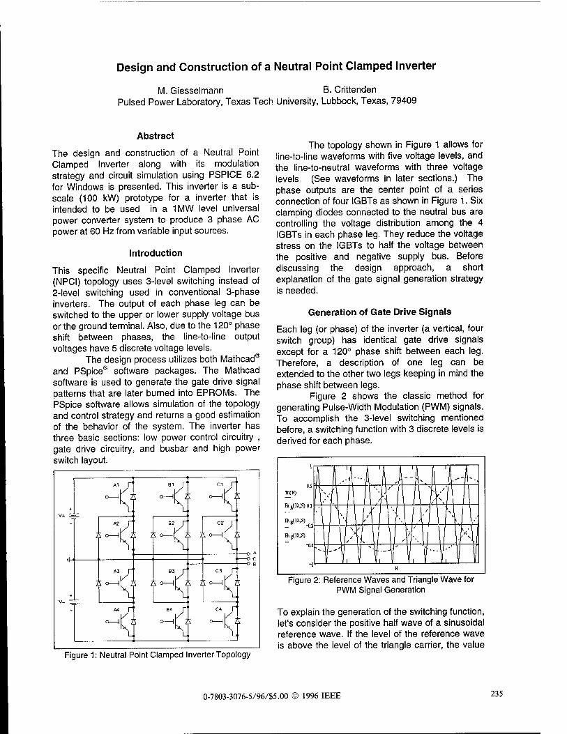
Design and Construction of a Neutral Point Clamped Inverter
M. Giesselmann B. Crittenden Pulsed Power Laboratory, Texas Tech University, Lubbock, Texas, 79409
Abstract
The design and construction of a Neutral Point Clamped Inverter along with its modulation strategy and circuit simulation using PSPICE 6.2 for Windows is presented. This inverter is a sub- scale (100 kW) prototype for a inverter that is intended to be used in a 1MW level universal power converter system to produce 3 phase AC power at 60 Hz from variable input sources.
Introduction
This specific Neutral Point Clamped Inverter (NPCI) topology uses 3-level switching instead of 2-level switching used in conventional 3-phase inverters. The output of each phase leg can be switched to the upper or lower supply voltage bus or the ground terminal. Also, due to the 120° phase shift between phases, the line-to-line output voltages have 5 discrete voltage levels.
The design process utilizes both Mathcad® and PSpice® software packages. The Mathcad software is used to generate the gate drive signal patterns that are later burned into EPROMs. The PSpice software allows simulation of the topology and control strategy and returns a good estimation of the behavior of the system. The inverter has three basic sections: low power control circuitry , gate drive circuitry, and busbar and high power switch layout.
<r< 4--
A2 r
C B2
ci n
c2 r
5 o—1[ $ $ o—1[ s L
B3 r
T T °—'N.
<
<
M r"
L
-O * -O C
c3 r
u B4 r" C4 f
o—iT i °—ir $
The topology shown in Figure 1 allows for line-to-line waveforms with five voltage levels, and the line-to-neutral waveforms with three voltage levels. (See waveforms in later sections.) The phase outputs are the center point of a series connection of four IGBTs as shown in Figure 1. Six clamping diodes connected to the neutral bus are controlling the voltage distribution among the 4 IGBTs in each phase leg. They reduce the voltage stress on the IGBTs to half the voltage between the positive and negative supply bus. Before discussing the design approach, a short explanation of the gate signal generation strategy is needed.
Generation of Gate Drive Signals
Each leg (or phase) of the inverter (a vertical, four switch group) has identical gate drive signals except for a 120° phase shift between each leg. Therefore, a description of one leg can be extended to the other two legs keeping in mind the phase shift between legs.
Figure 2 shows the classic method for generating Pulse-Width Modulation (PWM) signals. To accomplish the 3-level switching mentioned before, a switching function with 3 discrete levels is derived for each phase.
Figure 1: Neutral Point Clamped Inverter Topology
Figure 2: Reference Waves and Triangle Wave for PWM Signal Generation
To explain the generation of the switching function, let's consider the positive half wave of a sinusoidal reference wave. If the level of the reference wave is above the level of the triangle carrier, the value
0-7803-3076-5/96/$5.00 © 1996 IEEE 235
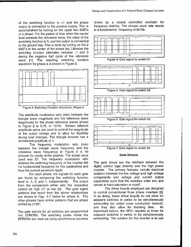
Design and Construction of a Neutral Point Clamped Inverter
of the switching function is +1 and the phase output is connected to the positive supply. This is accomplished by turning on the upper two IGBTs in a phase. For the period of time when the carrier level exceeds the reference wave, the value of the switching function is 0, and the output is connected to the ground bus. This is done by turning on the 2 IGBTs in the center of the phase leg. Likewise the switching function alternates between -1 and 0 during the negative half cycle of the reference wave [1]. The resulting switching function waveform for phase a is shown in Figure 3.
1.1
0J5
0
-0.55
1 1 1 1
1 1 1 1 H
Figure 3: Switching Function Waveform, Phase A
The amplitude modulation ratio (ratio between the triangle wave magnitude and the reference wave magnitude) for the phase reference waves shown in Figure 2 is 0.75, or 12/16. Sixteen different amplitude ratios are used to control the magnitude of the output voltage and to allow for flexibility during load changes. The triangle function has a normalized amplitude of 1.
The frequency modulation ratio (ratio between the triangle wave frequency and the reference wave frequency) in Figure 2 is 10 (chosen for clarity of the graphs). The actual value used was 27. The frequency modulation ratio dictates the switching frequency of the inverter (60 Hz fundamental frequency for this application) and thus the current waveform ripple.
For each phase, the signals for each gate are found by comparing the switching function level to -1, 0, and 1, independently. The output from the comparison either sets the respective control bit high (1) or low (0). The gate signal patterns that result from the above relationships are shown in Figs. 4-7 below for phase A. The other phases have similar patterns that are phase shifted by ±120°.
The gate signals for all switches are programmed into EPROMs. The switching codes inside the EPROMs are read out using synchronous counters
driven by a crystal controlled oscillator for frequency stability. The chosen clock rate results in a fundamental frequency of 60 Hz.
Figure 4: Gate signal for switch A1
Figure 5: Gate signal for switch A2
Figure 6: Gate signal for switch A3
Figure 7: Gate signal for switch A4
Gate Drivers
The gate drives are the interface between the digital control logic circuitry and the high power inverter. The primary features include electrical isolation between the low voltage and high voltage components and voltage and current output capabilities such that the switches enter into and remain in hard saturation or cutoff.
The driver boards employed are designed to control conventional three phase inverters [2]. In so doing, these driver boards do not allow for adjacent switches in series to be simultaneously conducting (so called cross conduction lockout), and they also allow for blanking time. As mentioned before, the NPCI requires at times for adjacent switches in series to be simultaneously conducting. The solution for this inverter is to use
236
Design and Construction of a Neutral Point Clamped Inverter
two driver boards with each board controlling two rows of switches. One board controls rows one and three (IGBTs A1, B1, C1, A3, B3, C3 in Fig.1), and the other board controls rows two and four (IGBTs A2, B2, C2, A4, B4, C4 in Fig. 1).
Switches, Diodes, and Busbar
Figure 1 shows the switch configuration along with the clamping diodes. Since the system constructed is of a prototype nature, the constraints on the devices need to be such that scaling laws can be developed for the actual system. Voltage and current ratings along with general switching performance (i.e. maximum) are the central concerns.
Due to the high switching speeds of the IGBTs, the connections between the switches and diodes need to have the lowest possible inductance. A layered busbar for connecting the devices provides the low inductance connections [3]. The dielectric material used as insulation between the layers of the busbar needs to have a breakdown voltage dictated by the bus voltages.
Description of Constructed System
Gate Drive Circuitry
The information in the EPROMs is delivered to the driver boards via simple digital circuitry. As mentioned above, a stable clock signal is generated from a higher frequency oscillator that has been reduced to the appropriate frequency by way of decade/binary counters. The clock signal drives a set of binary counters whose outputs are the address signals for the EPROMs. The two EPROMs use the same addressing hardware, but the outputs of the EPROMs go to the respective gate drive boards.
Driver Boards
The driver boards are Semikron SKHI60 models shown in Figure 8. The boards provide complete electrical isolation between the switches and the digital controller. The isolation voltage of the drivers is 2500 volts. The boards require 15 volt logic inputs so the outputs of the EPROMs are sent through level shifters to achieve the required input voltage. The driver boards also have other useful features. The boards monitor the collector- emitter saturation voltage during the on-time of each device in order to sense over-current conditions. The previously mentioned cross
conduction lockout feature can continue to be used as well as the blanking time feature. The driver boards are compatible with both metal-oxide- semiconductor FETs (MOSFET) and insulated gate bipolar transistors (IGBT).
JwwtTt': rjr.j*ihrj{A Vv»' '>''ir"\.ft
■^•JMWiil
§»e
.«MÄivürt WSW*»
Figure 8: Picture of a Semikron Driver board
Switches. Diodes, and Busbar
For the prototype, 600 V, 165 A IGBTs from International Rectifier were used for the switches, and the clamping diodes were 800 V, 45 A devices. The busbar was constructed from 0.040 inch thick aluminum with the dielectric being 0.030 inch thick plastic (Polyethylene). A cross section of the layout is shown in Figure 9. Figure 10 shows a photograph of the complete high power inverter assembly.
i/W/M/W//M/////////)/>MM//WWMWMM/'//'//)/////m////)/777777777T,
W/M^M/mMMM/M///MMm/mW/W/W////////MWW///MW,
\/i)w///wwwrm777T\ yi/wiwiiwim/nmm viwiimii/Mmimiimir-,_.,, ,H ,,,,,,,,\<- PtoseMput
f- +BusLfl)^f
*" Irwd Lwrr
k- -lus Layer
<- Ho* Uytr II
f Bo* Layer 12
mmMMMMmMMZMZMSSMMMEMMMMMM iiiiiiiiiwiiiii/imiMHiwiiiiiiiiiiiiiiiiitiiiiiiiiiiiiuiiiiiimimmmm,
W/////////////////////M mm iiiiiiinmiiiiiih wiMiiiiiiiiiwwirm wiii/iiiiiiiiiiiiiirm
KIT
tocUe
IGBI
wwiiiiiiwwiiunm. ü M3ZMMMZM n w
MT
Module
Figure 9: Layout of busbar
Figure 10: Switches, diodes, and busbar
237
Design and Construction of a Neutral Point Clamped Inverter
Output Waveforms and Results
Figures 11-14 show waveforms that were obtained from the NPCI system using a Tektronix PS222 digital storage oscilloscope. The data was then converted to a format suitable for the PSpice Post- Processor "Probe". During the tests, the inverter was driving a 1hp, 3-phase induction motor.
Figure 11: Gate drive signal, switch C1
2.00-
/J *~'i-rS '*f \
Oft- ^•H
-2.0A+- 0s
1(11) 10ns
Tine
1 20ns
Figure 12: Motor current, phase A
200U-
ou
"■r^iv,^ ,x
li . | ; I
iJ ULL
I i li III! T
-2O0U+- 0s
U(1) 10ns
Tine
1 20ns
Figure 14: Line-to-neutral voltage
Conclusions
A prototype of a neutral point clamped inverter has been build and successfully tested. This topology in combination with a suitable mechanical layout of the bus bar and professional driver boards seems a promising candidate for a high power inverter for a universal power converter.
References
1. S. Fukuda, K. Suzuki and Y. Iwaji, "Harmonic Evaluation of an NPC PWM Inverter Employing the Harmonic Distortion Determining Factor", Proceedings of the IEEE IAS Annual Meeting, October 1995, page 2417..2421.
2. SKHI 60 Data Sheet, Semikron Inc., 11 Executive Drive, P.O. Box 66, Hudson, NH 03051.
3. S. Upchurch, "Bus Bars Improve Power Module Interconnections", Power Conversion & Intelligent Motion, April 1995, p.18..25.
Acknowledgment
Acknowledgment: This work was sponsored by BMDO, Innovation Science & Technology. The contract was managed at USAF Wright Laboratory, Wright-Patterson AFB, Ohio.
Figure 13: Line-to-line voltage
238
FILAMENT HEATER CURRENT MODULATION FOR INCREASED FILAMENT LIFETIME
J. D. Paul, H. E. Williams, III Los Alamos National Laboratory, Los Alamos, NM 87545
Abstract
A circuit to eliminate 100 ampere heater currents from filaments during the arc pulse was developed. The magnetic field due to the 100 ampere current tends to hold electrons to the filament, decreasing the arc current. By eliminating this magnetic field, the arc should be more efficient, allowing the filaments to run at a lower average heater current. This should extend the filament lifetime. The circuit development and preliminary filament results are discussed.
Introduction
The surface conversion H-minus ion source employs two 60 mil tungsten filaments which are approximately 17 centimeters in length. These filaments are heated to approximately 2800 degrees centigrade by 95-100 amperes of DC heater current. The arc is struck at a 120 hertz rate, for 800 microseconds and is generally run at 30 amperes peak current. Although sputtering is considered a contributing factor in the demise of the filament, evaporation is of greater concern. If the peak arc current can be maintained with less average heater current, the filament evaporation rate for
this arc current will diminish. In the vacuum of an ion source, we expect the filaments to retain much of their heat throughout a 1 millisecond (12% duty) loss of heater current.
Modulator
As shown in figure 1, the modulator is configured as a difference amplifier comprised of power MOSFET devices so as to minimize the effect of large pulsed output currents oh the power supply regulation. The heater current through each of the filaments is controlled by a seperate difference amplifier to allow for balancing of the currents. The amplifiers are operated as closed-loop constant- current sources which can switch the current path from the filament
filament
Figure 1. Filament Modulator Layout
0-7803-3076-5/96/S5.00 © 1996 IEEE 239
Several problems were encountered during the development of the system. The first of these was cooling. The filaments operate at approximately 10 volts and 100 amperes which requires 1000 watts of power. The constant current source requires a minimum of 2.5- 3.0 volts to ensure proper operation. At 100 amperes, this circuit must dissipate 300 watts. The filament transistor handles about 100 watts. During the period in which the heater current is pulsed off, the other transistor is required to absorb the 1000 watts that the filament uses. The total average power dissipation is approximately 500 watts per amplifier so our modulator chassis had to be capable of dissipating 1000 watts without a significant temperature increase.
Since the chassis was intended for use in the H-minus Dome 80kV Equipment Rack, it had to be rack-mountable and as small as possible. Therefore, cooling requirements were of considerable importance. Another difficulty was the tendancy of electronic amplifiers to oscillate when switching large currents. Component selection and circuit layout were paramount to the stability of the system. Finally, we needed to protect the system from the high energy spikes which frequent the ground plane when the 80kV column in the Dome sparks to ground. The stored energy in one of these spikes can be upwards of 50 joules, more than sufficient to destroy most unprotected electronic components. Judicious selection and placement of assorted transzorbs and MOV's (metal-oxide Varistors) was required for operation in a high voltage environment. Nevertheless,
susceptibility to spark damage remains a problem.
Filament Modulator
Operation of the Filament Modulator is timed to ensure that the DC heater current is approximately zero and stable prior to the striking of the arc. The relative timing of the "Dump" gate, triggering the shunting of the heater current from the filament to the other transistor, and the "Source" gate, triggering the arc are shown in figure 2. The Dump gate begins approximately 100 microseconds prior to the Source gate to allow the filament to settle prior to applying the 200 volt arc pulse to the connection in figure 1. The Dump gate is 1000 microseconds long to extend approximately 100 microseconds beyond the falling edge of the arc pulse. This is to minimize sputtering of the filament and oscillations in the drive circuits. To maintain the necessary filament temperature for electron emission, we had to maintain a certain average heater current.
Dump Gate
lOOOus
Source Gate
800us
Figure 2. Relative Gate Timing
Therefore, the average heater currents were used to compare the "modulated" filaments with the "unmodulated" filaments. The standard by which we
240
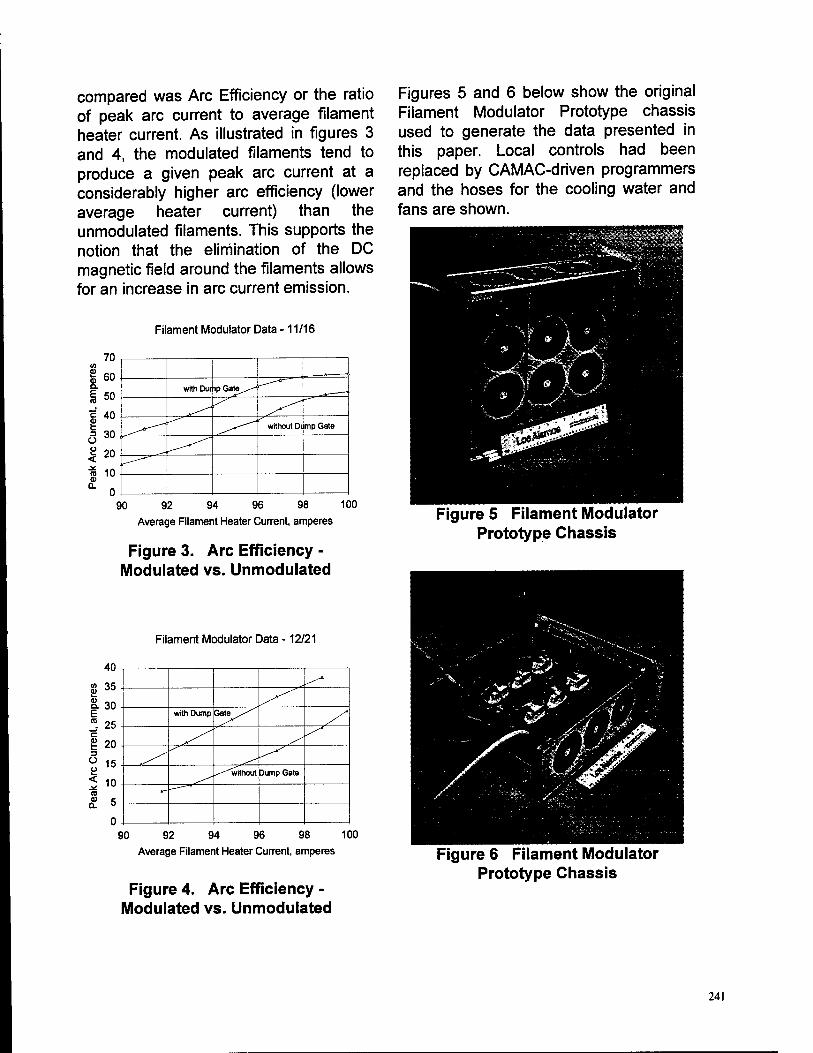
compared was Arc Efficiency or the ratio of peak arc current to average filament heater current. As illustrated in figures 3 and 4, the modulated filaments tend to produce a given peak arc current at a considerably higher arc efficiency (lower average heater current) than the unmodulated filaments. This supports the notion that the elimination of the DC magnetic field around the filaments allows for an increase in arc current emission.
Figures 5 and 6 below show the original Filament Modulator Prototype chassis used to generate the data presented in this paper. Local controls had been replaced by CAMAC-driven programmers and the hoses for the cooling water and fans are shown.
Filament Modulator Data -11/16
0) Q.
70
60
50
40
30
20
10
ft 1
withDui lpGate^--' ^ .
^^ without Di mpGate
-^
90 92 94 96 98 100
Average Filament Heater Current, amperes
Figure 3. Arc Efficiency - Modulated vs. Unmodulated
Filament Modulator Data -12/21
Figure 5 Filament Modulator Prototype Chassis
c g o Ü
(0 a a.
35
30
25 with Dump Gats/'' /
20
15
10 -
5 -
0 -
^^without Dump Gate
90 92 94 96 98 100
Average Filament Heater Current, amperes
Figure 4. Arc Efficiency - Modulated vs. Unmodulated
Figure 6 Filament Modulator Prototype Chassis
241

Conclusions
A compact, high current modulator prototype for the investigation into filament heater current effects has been designed and built. Preliminary test results show an increase in Arc Efficiency with a decrease in filament heater current during the arc pulse. Although the contributions of tungsten sputtering and arc current heating in the filament have not been addressed here, we may conclude that further studies could lead to a considerable improvement in filament lifetime.
Acknowledgements
The authors would like to thank Andrew Browman and Rob York for their assistance in the design and development of the modulator and Wade Potter for his expertise in the fabrication of the electronic and mechanical systems.
242

High Power C02-Laser at 100Hz Rep-rate
M. Jung, W. Mayerhofer, G. Renz and E. Zeyfang DLR, Institut für Technische Physik, Pfaffenwaldring 38-40,D-70569 Stuttgart, Germany
Introduction
The pulsed power issues in power conditioning for high power C02-lasers are related to the peak pulse voltage at the laser cavity, the pulse dura- tion, and the repetition frequency. For an electron beam sustained C02-laser system with an aver- age output power of more than 15kW, the pulse voltage at the modulator approaches the 50kV level with a pulse duration ranging from a few to a couple of ten microseconds or more. Electron beam sustained laser systems require an external preionization of the laser gas in order to reduce the load impedance of the laser cavity before the main discharge is initiated [1]. For short pulses, ranging from a few to ten microseconds, the cold-cathode type of electron beam accelerator (e-beam) is a suitable preionization scheme.
Table 1. Electrical concept of the laser system.
power supply modulator e-beam
100kJ/s 10» 10kJ/s parallel
30 kV
1 kJ/shot 30kV, 7.5kA
10kA/us main discharge
20 220 kJ/s
11 kJ/s parallel 50 kV
4 «500J/shot 50kV, 2kA
2kA/us
Furthermore, the power conditioning for repetitive pulsing at 100Hz requires a high precision of the interpulse period for the charging process and the charge control. With the advent of economical and reliable solid state components and the conversion from 60Hz to about 50kHz via high frequency in- verter circuits at the power supply system, a high reliability as well as a significant weight and vol- ume reduction has been achieved. This paper will present the design of the power conditioning equipment and the experimental verification of a repetitively pulsed high power C02-laser with an output power of more than 15kW, a pulse duration of 10 |xs, a pulse repetition rate of up to 100Hz, and a pulse train of 1000 shots.
Power conditioning of the laser system
The electrical design of the laser system divides the pulsed power parts of the e-beam and the main discharge C02-laser into three major sub- systems: the power supplies, the modulators (Pulse Forming Networks: PFNs), and the load (cf. Table 1). The efficiency of the C02-laser, defined by the ratio of the laser pulse output power to the electrical input power into the laser cavity, is com- monly known to be approximately 10%. A laser pulse energy of typically 150J and a repetition frequency of 100Hz requires a minimal electrical stored energy in the PFNs of 1.5kJ per pulse and a charging rate of 150kJ/s.
The power supply of the main discharge is divided into 20 parallel units (constant current moduls, Maxwell Laboratories) each having 11kJ/s at a loading voltage of 50kV. The voltage regulation of the power supply units is better than +/-0.05% [2]. At a repetition rate of 100Hz (10ms), the interpulse period for the charging process can take up to 8ms. The remaining 2ms are required for the charge control and the recovery of the spark gaps.The power supplies feed 4 modulators (PFNs) with an individual impedance of 12.5 Q (10 elements: L = 3u.H, C = .15uF, 10u.s duration, cf. Fig. 1), and a stored energy of 500J per pulse and per PFN [3].
4 PFNs each
12.5 fi
4 load - sections
4-10-20ft
As an electrical switch, a self-triggered air spark gap (Beverly III and Associates) with a super-sonic gas flow [4] is used for each individual PFN. At a loading voltage of 50kV, a current of 2kA, with a di/dt of 2kA/|is, is supplied from each PFN to the C02-laser gas load.
0-7803-3076-5/96/S5.00 © 1996 IEEE 243
4 main discharge modulators —\)
I Figure 1. Electrical circuits of the laser system.
The power supply system for the e-beam accelera- tor is divided into 10 parallel units, each having 10kJ/s. The loading voltage of max. 30kV can be regulated better than +/-0.05%. These power sup- ply units feed 2 PFNs with an impedance of 4.8 Q. (7 elements: L - 6 u.H, C = .3 pF, 10 us duration) at a stored energy of 1kJ per pulse.
2 PFNs each 4.8 ß
load primary 2.8 - 8 Ü,
The electrical switch of the e-beam is a triggered spark gap with a super-sonic air flow. The voltage of max. 30kV and the current of 7.5kA is then transformed with a pulse transformer (ratio 1:10, Stangeness) up to 200kV in the peak.
8i
0 2 4 6 8 10 12 14 16 18 20
time [us]
Figure 2. Impedance at the exit of the e-beam PFN
In Fig. 2 the impedance at the exit of the e-beam PFN is shown and Fig. 3 gives the secondary im-
pedance at the transformer. The impedance of the cold-cathode e-beam accelerator reaches a mini- mum of 2.8 Q. until the closure time ends the elec- tron extraction from the graphite plasma.The tem- poral behavior of the impedances is determined by the impedance of the e-beam PFNs, the parallel resistor Rp = 16 Q. (fluid resistor), the series resis- tor Rs = 0.6 Q. (low inductance resistor), and the e- beam load. The primary impedance stays relatively constant during the PFNs discharge time.The sec- ondary impedance rises in the first 2u.s to 1.5k£2 due to the cable impedance of approximately 200pF (AA 7583) between the transformer and the e-beam load; then the impedance falls off to nearly 0.3 k£2, which is determined by the series resistor FL
0 2 4 6 8 10 12 14 16 18 20
time [ps]
Figure 3. Impedance at the secondary side of the 1:10 transformer.
Volume specific power
The power supplies and the voltage reversal pro- tection unit for the e-beam accelerator take up 26kW/m3 of electrical volume specific power. The subsequent modulators (2 PFNs) amount to 45 kW/m3, including the gas switch and the trans- former. Due to the higher loading voltage of the main discharge system (max. 50kV), the power supplies and the voltage reversal protection unit occupy 40kW/m3. The modulators (4 PFNs), in- cluding the 4 gas switches, reach 100kW/m3 of volume specific power. The laser gas circulating system, including the discharge chamber and the electron beam accelerator vacuum unit, lead to a specific laser power of 2kW/m3. Since the devel- oped laser system is a prototype, the specifica- tions for the volume specific power have not yet been optimized. Reducing the overall volume of
244
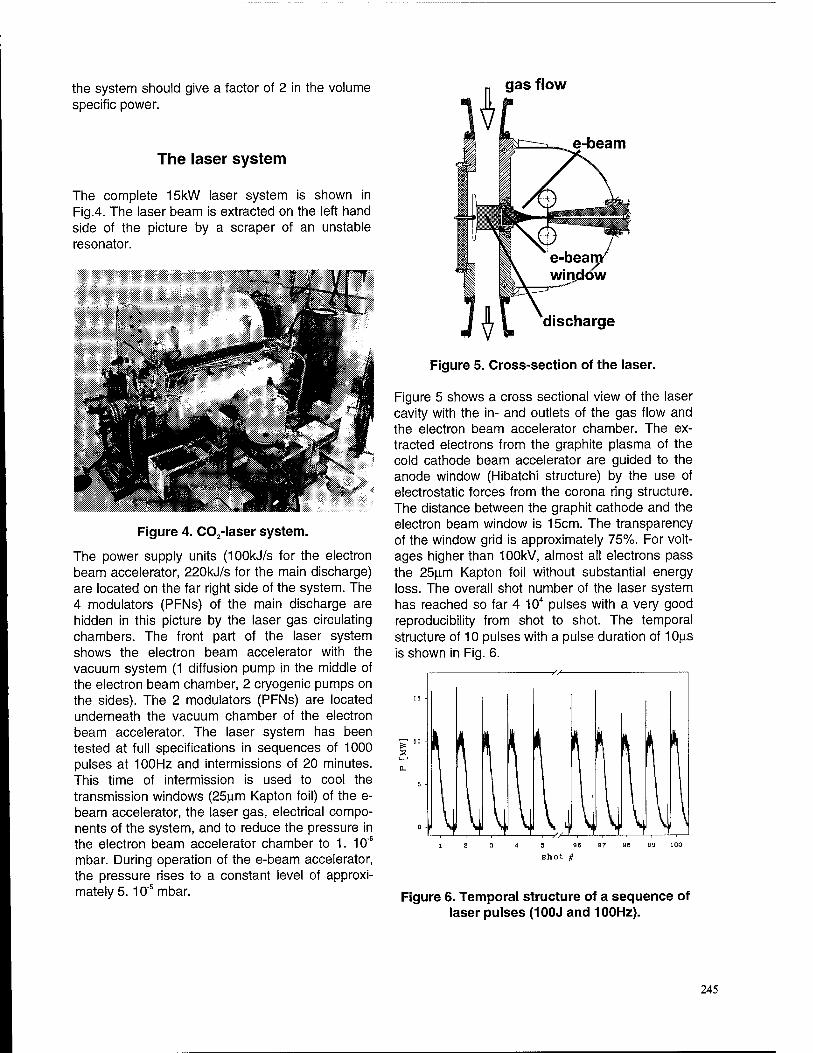
the system should give a factor of 2 in the volume specific power.
The laser system
The complete 15kW laser system is shown in Fig.4. The laser beam is extracted on the left hand side of the picture by a scraper of an unstable resonator.
gas flow
Figure 4. C02-laser system.
The power supply units (100kJ/s for the electron beam accelerator, 220kJ/s for the main discharge) are located on the far right side of the system. The 4 modulators (PFNs) of the main discharge are hidden in this picture by the laser gas circulating chambers. The front part of the laser system shows the electron beam accelerator with the vacuum system (1 diffusion pump in the middle of the electron beam chamber, 2 cryogenic pumps on the sides). The 2 modulators (PFNs) are located underneath the vacuum chamber of the electron beam accelerator. The laser system has been tested at full specifications in sequences of 1000 pulses at 100Hz and intermissions of 20 minutes. This time of intermission is used to cool the transmission windows (25u.m Kapton foil) of the e- beam accelerator, the laser gas, electrical compo- nents of the system, and to reduce the pressure in the electron beam accelerator chamber to 1. 10'6
mbar. During operation of the e-beam accelerator, the pressure rises to a constant level of approxi- mately 5.10"5 mbar.
e-beam
discharge
Figure 5. Cross-section of the laser.
Figure 5 shows a cross sectional view of the laser cavity with the in- and outlets of the gas flow and the electron beam accelerator chamber. The ex- tracted electrons from the graphite plasma of the cold cathode beam accelerator are guided to the anode window (Hibatchi structure) by the use of electrostatic forces from the corona ring structure. The distance between the graphit cathode and the electron beam window is 15cm. The transparency of the window grid is approximately 75%. For volt- ages higher than 100kV, almost all electrons pass the 25|j.m Kapton foil without substantial energy loss. The overall shot number of the laser system has reached so far 4 104 pulses with a very good reproducibility from shot to shot. The temporal structure of 10 pulses with a pulse duration of 10(j.s is shown in Fig. 6.
Figure 6. Temporal structure of a sequence of laser pulses (100J and 100Hz).
245
Synchronization of multiple modulators
In the charging sequence, the 4 modulators of the main discharge are loaded to max. 50kV. At an operating pressure of 0.5atm in the laser chamber and an interelectrode separation of 12cm, the self- breakdown voltage between the electrodes is ap- proximately 20kV. When using a voltage divider (cf. Fig. 1, CD1 = CD2 = 2nF), the voltage between the main discharge electrodes is kept below the self-breakdown limit until the electrons from the electron beam accelerator are drifting into the laser cavity. The impedance of the laser gas is then reduced and the full loading voltage appears be- tween the spark gap electrodes and initiates the breakdown in the switch.
I
I
§.
8 10 12 14 16 18 20
time [jis]
Figure 7. Voltage and current behavior of the electrical circuits.
This internal synchronization of multiple modula- tors shows a time jitter better than 100ns. The only trigger signal used in the system is the trigger pulse for the ignition of the electron beam accel- erator switch. In case of a misfunction of the e- beam accelerator, the energy of the main dis- charge is not transfered to the laser gas load since the discharge is non-selfsustained. This internal synchronization scheme is very cost effective and
very reliable in operation. In the upper part of Fig. 7, the voltage and current of the electron beam accelerator measured at the secondary output of the pulse transformer is shown. The middle part of this figure displays the loading voltage (40kV) of the PFNs recorded at the high voltage side of one of the gas switches. The lower part of the figure shows the voltage measured at the high voltage electrode of the main laser discharge, and the current into one of the 4 laser discharge elec- trodes. The voltage at the laser discharge elec- trode is kept at 16kV until the plasma impedance of the laser gas is reduced by the penetrating electrons. The voltage then drops to nearly zero until the spark gap switch makes the conduction to the high loading voltage of the PFNs.
Summary
The reliable operation of low cost spark gaps as modulator switches for 3kJ energy transfer per pulse at 100Hz and 1000 shots has been made possible by the use of high regulation capacitor power supplies in combination with the internal synchronization technique of the 4 main modula- tors.
References
[1] W.L. Bohn, 'High Power Gas Laser Re- search in Germany', in: Gas lasers- recent devel- opments and future prospects, NATO ASI Series, 3. High Technology- Vol.10, Klüver Academic Pub- lisher (1996).
[2] E. Strickland, F. Cathell, K. Harris, D. Bi- lak, and J. Jichetti, 'High regulation, capacitor charging power supplies', Maxwell Laboratories Inc., San Diego, Ca., presented at the 1995 SPIE Conference in San Jose, Ca., USA.
[3] M. Jung, W. Mayerhofer, Th. Schweizer, and E. Zeyfang, 'Spark gap switched PFN's op- erating at 100Hz for a multi kW pulsed C02 laser, IEEE Pulsed Power Conf., Albuquerque, (1995).
[4] R.E. Beverly III and R.N. Campbell, 'Transverse-flow 50-kV trigatron switch for 100-pps burst-mode operation', Review of. Scientific Intru- ments, Vol. 67, p. 1593(1996).
246
SIX PULSE BRIDGE CONVERTER FOR RAPID CONSTANT CURRENT CHARGING OF MEGAJOULE PFNS
G. L. SCHOFIELD, N. C. JAITLY AND E. Y. CHU MAXWELL LABORATORIES
SAN DIEGO, CA
AND
R. ELWELL NAVAL SURFACE WARFARE CENTER
ANNAPOLIS, MD
Recently, a 4.8 MW, transformerless, three phase, 60 Hz, ac to dc, SCR controlled, converter was designed, fabricated and successfully tested at Maxwell Laboratories, Inc. for use in the Navy ETC Gun Technology program. It can provide a maximum of 20 kV output into either a capacitive or resistive load. Power to the converter input will be provided by a dedicated 13.8 KV, three phase 60 Hz, synchronous generator. With a 4 MVA generator, this combination is capable of charging a 4 MJ bank to 15 kV in 2 seconds. The converter incorporates two 17.5 mH, 300 A, air core current limiting inductors, one in series with each output connection. These inductors' support the voltage difference between the converter's instantaneous output and the PFN voltage while limiting output current and maintaining efficiency. A freewheeling diode is connected across the output between the bridge and current limiting inductors and directs the inductors' stored energy into the PFN during periods of discontinuous conduction or during fast turn off of the bridge. A compensated negative feedback loop controls the delay angle of the SCR trigger pulses to produce stable, constant current charging and voltage limiting to the PFN load. A leg of the SCR full wave three phase bridge consists of 5 series SCRs, each with a PIV rating of 6500 V. A specially designed low leakage transformer was mounted near each leg of the bridge to provide simultaneous triggering of the seriesed SCRs and high voltage isolation for the gate pulse firing board. The operator interface consisted of 66 MHz 486 running Lab VIEW® 3.0 Connections between the computer controller and the converter were exclusively by the optical fiber.
One unique aspect of the converter design is the feedback loop compensation required to produce stable bridge converter operation into the series combination of current limiting inductance and PFN capacitance. Another challenging aspect of the design was the use of seriesed SCRs for the direct control and rectification of 13.8 kV three phase lines with no intervening power transformers. Our solutions to these design problems are discussed, and pertinent test data are presented demonstrating the success of the design. This converter will be used to support the development of on-ship dc power conversion equipment for Navy pulsed power applications.
0-7803-3076-5/96/S5.00 © 1996 IEEE 247

LIST OF ATTENDEES
Forrest Agee Phillips Laboratory 3550 Aberdeen Ave PL/WSQ Kirtland Afb, NM 87117-5776 (505) 846-2824
Sean Ahern Maxwell Laboratories, Inc. 2501 Yale SE, Suite 300 P.O. Box 9350 Albuquerque, NM 87199 (505)846-9073
Harish Anamkath Titan Beta 6780-R Sierra Court Dublin, CA 94568 (510)828-0555
Steven Babcock Sandia National Laboratories P.O. Box 5800 MS-1153 Albuquerque, NM 87185-1153 (505) 844-3437
David Baggest Electrical Engineer General Atomics PO Box 85608 San Diego, CA 92186-9784 (619)455-4152
David Barrett QM Technologies 3701 Hawkins St NE Albuquerque, NM 87109 (505)342-2851
Leon Bartelson Fermilab P.O. Box 500, M/S 308 Batavia,IL 60510 (708) 840-4065
George Bees ALE/EMI 241 Boston Post Road Marlborough, MA 01752 (508) 480-8966
Paolo Bettini Instituto Gas Ionizzati - CNR Associazioni EURATOM-ENEA-CNR Unv Padova Corso Stati Uniti 4 Padova, 35127 Italy 39 49 8295000
Dan Borovina Univ. of Texas at Dallas Ctr for Quantum Elect. 2601 N. Floyd Rd,NB 11 Richardson, TX 75080 (214)883-2863
Ken Bourkland Fermilab POB 500 M/S 308 Batavia,IL 60510 (708) 840-3813
Christopher Braun Colorado School of Mines Division of Engineering Golden, CO 80401
Paul Brown Range Systems Engrg, Raytheon KREMS, Roi-Namur P.O. Box 997 APO, AP 96557
Malcolm Buttram Sandia National Laboratories HPE Dept. P.O. Box 5800, MS 1153 Albuquerque, NM 87185-1153 (505)845-7117
248

LIST OF ATTENDEES
William Carey Univ. of Texas at Arlington Applied Physical Elect Rsch Ctr P.O. Box 19380 Arlington, TX 76019-0380 (817)272-5109
Richard Cassel Standford Linear Accel. Ctr 2575 Sand Hill Rd M/S 49 Menlo Park, CA 94025
Daniel Chatroux CEADTE/SLC/SDL P.B. 111 Pierrelatte, Cedex 26702 France 75-50-75-63
Cassio Conceicao ETM Electromatic, Inc. 35451 Dumbarton Ct. Newark, CA 94650 (510)797-1106
Alexander Cours Argonne National Laboratory APS-ASD-RF Bldg 401 Room C3249 9700 South Cass Avenue Argonne, IL 60439 (708) 252-4550
Carl Crager Litton Systems, Inc. Electron Devices Division 1035 Westminster Drive Williamsport, PA 17701 (717) 326-3561
Charles Crist Sandia National Laboratories P.O. Box 5800 MS-1153 Albuquerque, NM 87185-1153 (505) 844-7148
Farzin Davanloo Univ. of Texas at Dallas Center for Quantum Electronics 2601 N. Floyd Rd.,NB 11 Richardson, TX 75080 (214) 883-2267
James Dickens Texas Tech University 1914 49th Street Pulsed Poser Laboratory Lubbock,TX 79408-3102 (806) 742-1254
William Dunbar Consultant 1065 149th PISE Bellevue, WA 98007 (206) 746-1274
Vladimir Efanov Ioffe PTI of Russian Academy of Science Politechnicheskaja 26 St Peterburg, 194021 Russia 78122479957
Harald Eizenhofer Dornier Medizintechnik Postfach 11 28 Germering, D-82101 Germany
Fumihiko Endo Toshiba Corp 1 Toshiba- cho, Fuchu-shi Tokyo, 183 Japan 81423332557
G. Andrew Erickson Los Alamos National Lab. PO Box 1663 M/SH851 Los Alamos, NM 87545 (505) 665-3567
249

LIST OF ATTENDEES
Klaus Frank University of Erlangen Erwin-Rommel-Str. 1 Erlangen, D 91058 Germany 9131-857147
Marcel Gaudreau Diversified Technologies Inc. 35 Wiggins Ave Bedford, MA 01730 (617)275-9444
Frank Gekat Gemarronik GmbH Raiffeisenstrasse 10 Neuss, D-41470 Germany
Michael Giesselmann Texas Tech University MS 3102 Dept. of Elect. Eng. Lubbock,TX 79409-3102 (802) 742-3462
William Glodzik FTVR Advanced Power Components 1576 Sweet Home Road Suite 210 Amherst, NY 14228 (716)639-1603
Dan Goebel Hughes Telecommunications & Space Co. Electron Dynamics Division 3100 W. Lomita Blvd., TO/230/1010 Torrance, CA 90509 (310)517-5127
Michael Grothaus Southwest Research Institute 6220 Culebra Road P.O. Drawer 28510 San Antonio, TX 78228-0510 (210) 522-6676
Henry Grunwald Triton Electronic Technology Division 3100 Charlotte Avenue Easton, PA 18042 (610)252-7331
Martin Gundersen Univ. of Southern California Dept. of E.E.E. University Park Los Angeles, CA 90089-0484
Peyman Hadizad Motorola, Inc. 5005 E McDowell Road Z-311 Phoenix, AZ 85008 (602) 244-6304
Jud Hammon Physics International 2700 Merced Street 7400a San Leandro,CA 94577 (510)577-7118
Shirikant Hangirgekar SAMEER LIT. Campus Powai Mumbai, 400076 India 091 022 578 3227
Lynn Hatfield Texas Technical University Pulsed Power Laboratory Physics Dept, MS-1051 Lubbock,TX 79409-1051 (806) 742-1250
Stuart Hesselson Marketing Manager EEV, Inc. 4 Westchester Plaza Elmsford, NY 10523 (914)592-6050
250

LIST OF ATTENDEES
Bill Hodges Colorado School of Mines Division of Engineering Golden, CO 80401
Robert Hoeberling Los Alamos National Laboratory Box 1663 MSH851 Los Alamos, NM 87544 (505) 667-9722
Dale Hollis Reynolds Industries, Inc. 5005 McConnell Avenue Los Angeles, CA 90066 (310)823-5491
Douglas Horan Argonne National Laboratory APS-ASD-RF Bldg 401 Room C3270 9700 South Cass Avenue Lemont, IL 60439 (708) 252-7565
Jon Hull USAF 8640 Horacio Place NE Albuquerque, NM 87111 (505)296-9215
Frank Idel Gematronik GmbH Raiffeisenstrasse 10 Neuss, D 41470 Germany 49-2137-782-217
Ray Jaitly Maxwell Laboratories 9244 Balboa Avenue San Diego, CA 92123 (619) 576-7714
David Jordan UK Defense Research Agency Weapons Systems Sector Bldg. R14 Farnborough, Hants GU14 6TD UK 44(0)1252-392011
Markus Jung DLR Institut Fur Technische Pysik Pfaffenwaldring 38-40 Stuttgart, D-70569 Germany 49-711-6862-646
Alexei Kardo-Sysoev Ioffe PTI of Russian Academy of Science Politechnicheskaja 26 StPeterburg, 194021 Russia (819)247-9996
Kenneth Karsten Triton Electron Technology Division 3100 Charlotte Ave. Easton, PA 18042 (610)252-7331
Brian Kerr DRA Malvern St. Andrews Road L215 Malvern, Worcs WR14 3PS England 01684 894949
John Kinross-Wright Los Alamos National Lab AOT-9,MSH851 Los Alamos, NM 87545 (505)665-1181
Johnelle Korioth University of Texas At Dallas Center for Quantum Electronics 2601 N. Floyd Rd,NB 11 Richardson, TX 75080 (214) 883-2863
251

LIST OF ATTENDEES
Richard Korzekwa Los Alamos National Laboratory P.O. Box 1663 E-252 Los Alamos, NM 87545 (505) 665-8422
Rudolph Limpaecher DC Transformation, Inc. 181 Elliott Street Suite 711 Beverly, MA 01915 (508)921-5505
Diana Loree USAF Phillips Laboratory 3550 Aberdeen Ave., SE Kirtland AFB, NM 87117-5776 (505) 846-5496
Guillermo Loubriel Sandia National Laboratories P.O. Box 5800 MS 1153 Albuquerque, NM 87185-1153 (505)845-7096
Lawrwence Luessen Naval Surface Warfare Center Directed Energy Branch CodeF12 Dahlgren, VA 22448
Scott Macgregor University of Strathclyde Dept Electronic & Electrical Engrng 204 George Street Glasgow, Gl 1XW Scotland 44-141-552-4400
Edgar Malone Reynolds Industries Inc 366 Silva Place Nipomo, CA 93444 (805) 929-3677
Michael Marks EG&G Inc. 35 Congress Street MS01 Salem, MA 01970 (508) 745-3209
John Marous ABB High Power Semiconductors 575 Epsilon Dr Pittsburgh, PA 15238-2838 (415)967-5858
Jaques Maury CEA DTF/SLC B.P. Ill Pierrelatte, Cedex 26702 France 75-50-43-24
Jon Mayes University of Texas At Arlington Applied Physical Elect. Res. Ctr. P.O. Box 19380 Arlington, TX 76012-0380 (817)272-5111
Andrew McPhee AMS Electronic Ltd Castle Circus House 136 Union Street Torquay, Devon TQ2 5QG UK 44 1454 417771
Hugh Menown EEVLtd. 106 Waterhouse Lane Chelmsford, Essex CM12QU U.K. 44 1245 493493
Klaus Metzmacher CERN European Org for Nuclear Res Geneva 23, 1211 Switzerland 010-41-22-7674426
252

LIST OF ATTENDEES
Jian-Lin Mi Brookhaven National Lab AGS Dept. 911 B Upton, NY 11973-5000 (516)344-4619
Gary Miscikowski Maxwell Laboratories, Inc. 4949 Green Craig Lane San Diego, CA 92123 (619)576-7545
Stuart Moran Naval Surface Warfare Center 17320 Dahlgren Road Bldg. 424t Code B20 Dahlgren, VA 22448-5100
Matthew Myers Naval Research Laboratory 4555 Overlook Ave, SE Code 6751 Washington, DC 20375-5346 (202) 767-7530
John Naff Physics International 2700 Merced St, PO Box 5010 San Leandro, CA 94577-0599 (510)577-7276
J.Nel AEC of South Africa Po Box 582 Pretoria, 0001 South Africa
Richard Ness CYMER Laser Technologies 16275 Technology Dr San Diego, CA 92127 (619)487-2442
Johann Nett French-German Research Institute 5 Rue Du General Cassagnou Saint-Louis, F 68301 France 33-8969-5067
William Nunnally APERC Univ of Texas at Arlington P.O. Box 19380 Arlington, TX 76012-0380 (817)272-5110
R. Nylander Varian Oncology Systems 611 Hansen Way, M/S C077 Palo Alto, CA 94303-1028 (415) 424-6898
James O'Loughlin USAF Phillips Lab PL/WST 3550 Aberdeen Ave., SE Blgd 66071 Kirtland AFB, NM 87117-5776 (505) 846-5496
Jong-Seok Oh PAL/POSTECH San 31 Hyoja-dong, Nam-ku, Pohang Kyungbuk, 790-784 Korea 82-562-279-1145
Soung-Soo Park PAL/POSTECH San 31 Hyoja-dong, Nam-ku, Pohang Kyungbuk, 790-784 Korea 82-562-279-1145
Mark Parsons Los Alamos National Lab PO Box 1663 MS E548 Los Alamos, NM 87545 (505) 667-7872
253

LIST OF ATTENDEES
Ronald Pate Sandia National Laboratories P.O. Box 5800 Dept. 9512, MS-1153 Albuquerque, NM 87185-1153 (505) 844-3043
Jerome Paul Los Alamos National Laboratory PO Box 1663 MS P947 Los Alamos, NM 87545 (505) 667-5477
Mark Pease Raytheon RES 50 Apple Drive M/S T2SF1 Tewksbury, MA 01876 (508)858-1408
Colin Pirrie EEV Ltd. 106 Waterhouse Lane Chelmsford, Essex, CM12QUU.K. 44 1245 453644
Thomas Podlesak Army Research Laboratory Atta: AMSRL-WT-NH Fort Monmouth, NJ 07703-5601 (908) 427-2888
Alexander Pokryvailo SoreqNRC Yavne, 81800 Israel 972(8)9434490
William Portaoy Texas Tech University Dept. of Electrical Engineering Lubbock, TX 79409 (806) 742-3532
John Power Los Alamos National Lab POB 1663 M/S H808 Los Alamos, NM 87545
Lu Pullia Ontario Hydro Technologies 800 Kipling Avenue KT110 Etobiooke, Ont. Canada (416) 207-5466
Darren Qunell Fermilab P.O. Box 500 Kirk & Wilson Road, MS 308 Batavia,IL 60510 (708) 840-3530
Esie Ramezani ABB Semiconductors AG Fabrikstr 3 Lenzburg, CH5600 Switzerland 4162 8886 370
Sulabha Ranade SAMEER I.I.T. Campus Powai Mumbai, Muharashtra 400076 India 091 022 578 3227
Juan Ramirez Member Tech Staff Sandia National Laboratories Dept. 9310 MS 1178 Albuquerque, NM 87185-1178 (505) 845-7052
William Reass Los Alamos National Lab Box 1663 MS-E526 Los Alamos, NM 87544 (505) 665-1013
254

LIST OF ATTENDEES
Kim Reed Sandia National Laboratories P.O. Box 5800 MS 1152 Albuquerque, NM 87185-1152 (505)845-7109
Günther Renz DLR, Institut Fur Technische Physik Pfaffenwaldring 38-40 Stuttgart, D-70569 Germany 49-711-6862-249
Natalie Ridge University of St. Andrews North Haugh School of Physics and Astronomy St Andrews, FIFE KY10 2RE Scotland
Larry Rinehart Sandia National Laboratories P.O. Box 5800 MS-1153 Albuquerque, NM 87185-1153 (505)845-3104
Rigoberto Rodriguez DC Transformation, Inc. 181 Elliott Street Suite 711 Beverly, MA 01915 (508) 921-5505
Gerald Rohwein Sandia National Laboratories P.O. Box 5800 MS 1153 Albuquerque, NM 87111 -1153 (505) 845-7350
Lars Roose Sandia National Laboratories P.O. Box 5800 MS 1153 Albuquerque, NM 87185-1153 (505) 845-7359
Chris Rose Los Alamos National Lab P.O. Box 1663 H808 Los Alamos, NM 87545
Frank Rose Director Space Power Institute 231 Leach Center Auburn University, AL 36849-5320 (334) 844-5894
Randy Roush Naval Surface Warfare Center 17320 Dahlgren B20 Dahlgren, VA 22448 (540)653-8026
Neil Rubado EG&G 35 Congress Street Salem, MA 01970 (508) 745-3200
Kenneth Rust Los Alamos National Laboratory PO Box 1663 M/SH838 Los Alamos, NM 87545 (505) 665-2606
W. Sarjeant University At Buffalo - SUNY/AB Bonner Hall -Rm 312 PO Box 601900 Buffalo, NY 14260-1900
George Schaller Ceramic Magnetics, Inc. 16 Law Drive Fairfield,NJ 07004 (201) 227-4222
255

LIST OF ATTENDEES
Sol Schneider Consultant 100 Arrowwood Court Red Bank, NJ 07701 (908) 741-7429
Karl Schoenbach Old Dominion University Dept of E.C.E. Physical Electronics Rsch Inst. Norfolk, VA 23529-0246 (804)683-4625
George Schofield Maxwell Laboratories, Inc. 9244 Balboa Avenue San Diego, CA 92123 (619) 576-7890
Gerhard Schroder CERN SL Division Geneva 23, 1211 Switzerland 41-22-767-4825
Dan Schweickart Wright Laboratory POOS- 2 Bldg. 450 Wright-Patterson AFB, OH 45433 (513)255-9189
Stephen Shpock Litton Systems, Inc. Electron Devices Division 1035 Westminster Drive Williamsport, PA 17701 (717)326-3561
John Sethian Plasma Physics Division Naval Research Laboratory 4555 Overlook Avenue Code 6730 Washington, DC 20375 (202) 767-2705
Anton Shulski Richardson Electronics, Ltd. 40W267 Keslinger Road LaFox.IL 60147 (708) 208-2300
Robert Sikora Westcode Semiconductors 3245 Hyde Park Dr. Clearwater, FL 34621 (813)787-4612
Arnold Silva Member Technical Staff NASA-JPL 4800 Oak Grove Drive Pasadena, CA 91109 (818)354-7390
Dave Singh US Army Research Lab ARL-WTD AMSRL-WT-NH Ft. Monmouth, NJ 07703 (908)532-0271
Israel Smilanski NRCN PO Box 9001 Beer-Sheva, Israel 972-7-567606
Ian Smith Titan/Pulse Sciences Inc. 600 McCormick Street San Leandro, CA 94577
Paul Smith Oxford University Engineering Science Parks Road Oxford, OX1 3PJ England 011865273039
256
LIST OF ATTENDEES
Emil Spahn French-German Research Institute 5 Rue Du General Cassagnou Saint Louis Cedex, F 68301 France 33-8969-5197
Alexander Stewart Army Research Labs 2800 Powder Mill Rd AMSRL-WT-NH Adelphi, MD 20783 (301)396-3240
Steve Turnbull University of Strathclyde Dept Electronic & Electrical Engineering 204 George St Glasgow, G11XWUK 44 141 552 4400 x2376
Lawrence Turner US Army 220 7th Street, NE Charlottesville, VA 22901 (804)980-7899
David Turnquist Litton Systems, Inc. Electron Devices Division 1035 Westminster Drive Williamsport, PA 17701 (717)326-3561
Andrew Tydeman British Aerospace Dynamics P.O. Box 5, Filton MS: FPC 500 Briston, Avon BS12 7QW UK 44-117-9316929
Mario Vescovi INFN-LNF Via E.Fermi No. 13 Frascati, 00044 Italy 39-6-94032256
Eugene Vossenberg Cern SL Division Geneva 23, 1211 Switzerland 41-22-767-4811
Lawrence Walko WL/POOX-2 WRDC/POOX-3 Wright-Patterson AFB, OH 45433
F. Thomas Warren Physics International Co 2700 Merced St P.O. Box 5010 San Leandro, CA 94577-0599 (510)577-7251
Ju Wang APS360 Argonne National Laboratory 9700 S. Cass Avenue ASD/401-C3244 Argonne, IL 60439 (708) 252-4340
Clifford Weatherup EEV Ltd. 106 Waterhouse Lane Section 9 Chehnsford, Essex CM12QU U.K. 44 1245 453491
Richard Wheeler Los Alamos National Laboratory PO Box 1663 Los Alamos, NM 87545
Harry Williams Los Alamo National Laboratory AOT-2, H-838 Los Alamos, NM 87545 (505) 667-3834
257

LIST OF ATTENDEES
Jon Williams Electronic Measurements Inc. 405 Essex Road Neptune, NJ 07701 (908) 922-9300
Michael Wilson Lawrence Livermore Labs POB 808 L153 Livermore, CA 94550 (510)424-4011
David Yanko HVR Advanced Power Components 3380 Sheridan Drive Suite 410 Amherst, NY 14226 (716)639-1603
Chris Young Unison Industries 7575 Baymeadows Way Jacksonville, FL 32256 (904) 739-4289
Robert Zeto Army Research Laboratory AMSRL-PS-DA Physical Sciences Directorate Ft Monmouth,NJ 07703 (908) 427-4872
Jennifer Zirnheld SUNY At Buffalo 312 Bonner Hall Box 601900 Amherst, NY 14260-1900 (716)645-2422
Fred Zutavern Sandia National Laboratories P.O. Box 5800 MS 1153 Albuquerque, NM 87185-1153 (505)845-9128
258

Author Index
A Agee, F.J 1,26, 181 Altes, R.A 177 Anamkath, H 101 Aurand, J.F. 165
B
Baca, A.G 31 Beerwald, M 108 Behr, S 43 Bettini, P. 137 Bhasavanich, D 161 Blokesch, G 108 Borovina, D.L 26, 181 Braun, C 169,232 Bridges, J 55 Brown, D.J 165 Brown, P. 125 Bruderer, G 71 Brylevesky, V.I 39, 51 Burke, T. 18 Bush, M 213,222 Buttram, M.T. 165
C Calico, S.E 218 Carey, W.J 113 Carson, S 47 Case, M.J 85 Cho, M.H 186, 190 Christiansen, J 129 Chu, E.Y. 247 Coates, D 97 Collins, C.B 26, 181 Corcoran, PA 177 Crittenden, B 235
D
daSilva, T. 161 Davanloo, F. 26, 181 Davis, H 97 Dickens, J.C 55 Dollinger, R.E 198,209 Dollinger, S 129 Ducimetiere, L 67, 149 Dvorak, J 169,232
E Efanov, V.M 22, 39, 51 Elmoursi, A 93 Elwell, R 247
Endo, F. 63
F
Farish, D 153 Faure, P. 149 Felsner, P. 129 Fernsler, R.F. 118 Flemish, J.R 18 Foley, V.G 198 Fox, T.J 75 Frank, K 129
G
Gatewood, M 213,222 Gekat, F. 108 Giesselmann, M 47, 235 Gilman, CM 161 Goldberg, H 209 Görtier, A 129 Gower, F. 101 Gregor, J.A 118 Grothaus, M.G 79 Gundersen, M.A 15
H
Hadizad, P. 35 Hammon, J 157, 161 Hangirgekar, S.G 202 Harrower, J 194 Heine, F. 129 Helgeson, W.D 31,165 Hintz, G 129 Hjalmarson, H.P. 31 Hodges, B 169,232 Hoffman, D.H.H 129 Hull, J.H 26,181 Hutcherson, R.K 79
I
Idel, F. 108 III, R.W.AIden 75 Ingram, M.W 79
J
Jaitly, N.C 247 Jang, G.H 186 Jang, S.D 186 Jansson, U 67,149 Joshi, M.Y. 202 Jung, M 173,243
K Kakizaki, K 63 Kaneko, E 63 Kanter, M 228 Kardo-Sysoev, A.F. . 22, 39, 51 Kiekel, PD 205 Kingsley, LE 26, 181 Ko, I.S 186 Korioth, J.L 26, 181 Krause, R.K 26, 181 Kristiansen, M 55
L
Lam, S.K 157 Limpaecher, R 213,222 Loree, D.L 218 Lorenzi, A.De 137 Loubriel, G.M 31, 165
M MacGregor, S.J. 145,153,194 Mahund, Z 47 Maitland, A 133 Malaczynski, G. .. 93 Mathew, J 118 Mayerhofer, W. .. 173,243 Mayes, J.R 113 McCordic, C 125 McGeoch, M.W. .. 177 McPhee, A.J 145 Meger, R.A 118 Mendonsa, R. 101 Miller, R 101 Munson, C.A. 93 Murphy, D.P. 118 Myers, M.C 118
N
Namkung, W 186, 190 Nel, J.J 85 Nielsen, K 161 Nunnally, W.C 113
O O'Loughlin, J.P 218 O'Malley, M.W 31, 165 Obenschain, S.P 177 Oh, J.S 186, 190 Okamura, K 63 Olson, J 97 Ommen, J 35
259

Author Index
P
Park, S.S 186, 190 Park, S.W 190 Parkes, D.M 133 Patro, Y.G.K 122, 202 Paul, J.D 239 Pechacek, R.E 118 Podlesak, T.F. 18,43 Pokryvailo, A 228 Pomeroy, S 157 Prucker, U 129
R
Ramezani, E 71 Ramirez, J.J 5 Ranade, S.R 122, 202 Reass, W.A 89, 93, 97 Reed, K.W 205 Renz, G 173,243 Ridge, N.A 133 Riege, H 149 Rieger, M 173 Robles, E 35 Rodriquez, R 213, 222 Rohwein, G.J 59, 141 Roose, L.D 59 Rose, M.F. 9 Roush, R.A 79 Ruebush, M.H 31
S
Salih, A 35 Sarjeant, W.J 198,209 Schlaug, M 67,149 Schleinitz, H 97 Schneider, S 43 Schoenbach, K.H 75 Schofield, G.L 247 Schröder, G 67, 149 Schwandner, A 129 Sethian, J.D 177 Shaked, N 228 Shaw, R 161 Shevgaonkar, R.K 122 Silva, A 104 Singh, H 18,43 Slocomb, R 35 Smirnova, I .A 39 Smith, I.D 177 Spahn, E 71 Steudel, M 125 Swart, P.H 85
T
Takagi, S 63 Tchashnikov, I.G. ... 22, 39, 51 There-, C 35 Tidmarsh, J.R 145 Tuem, F.A 153
Tuema, F.A. 194 Turnbull, S.M 153, 194
V
Varadarajan, S 35 Vinacco, K 213, 222 Vossenberg, E 67, 149
W
Whitman, K 101 Williams, III, H.E 239 Wölk, M 35 Wood, B.P. 89
X
Xie, K 18
Y
Yarin, P.M 22
Z
Zante, A 101 Zeyfang, E 173,243 Zhao, J.H 18 Zirnheld, J.L 198,209 Zutavern, F.J 31, 165
260


