Embed Size (px)
Citation preview
193 nm Photo-Resist Shrinkage after Electron Beam Exposure
Bo SUa, Guy Eytan', and Andrew Romano'aprocess Diagnostics and Control Group, Applied Materials, Inc.
bElectronic Materials Business Unit, Clariant Corp.
ABSTRACT
In addition to stability and collapse issues facing 1 93 nm resists, a new concern is rising regarding line width decrease whenexposed to an electron beam (e-beam) during CD measurements using scanning electron microscope (SEM). Such aninteraction between the measurement system and sample materials poses a great challenge in process development for 193urn lithography which is believed to be next lithography node. This paper reports the investigation results of 193 nm resistline width slimming under e-beam. We have observed vertical, as well as lateral 1 93 nm resist shrinkage under e-beamexposure using VeraSEM 3D's unique sidewall imaging technology. We have observed different CD changing behaviors forlines and spaces, as expected. Repeated SEM CD measurements on a space magnify the CD changing effect due to 3-5 timesmore resist exposed to the e-beam than a line. Hence, the influence of other competing effects from line edge roughness,carbonization etc. are reduced. By measuring a space or an edge width at a tilted view, the severity of resist shrinkage ofdifferent resist types can be compared directly with a high level of confidence.
INTRODUCTION
Critical issues, such as stability and collapse encountered in 193 nm resist development may delay the deployment of 193 nmlithography even though 1 93 nm scanners are commercially available. Recently, another issue associated with 1 93 nm resistshas been discovered: resist lines shrink when exposed to an electron beam (e-beam) [1-3]. Such a strong interaction betweena metrology tool and a sample poses a great challenge in 193 nm resist CD metrology. Repeated CD measurements by a CD-SEM on a 193 nm resist line are highly undesirable when CD changes are induced during SEM CD measurements. Thisstudy aims to understand the shrinkage phenomenon, not to provide a solution. However, based on the fmding of the study,we will suggest a few general rules on how to reduce the interaction effect between CD-SEM and 1 93 nm resist features to bemeasured.
Resist shrinkage has been observed even in 248 nm resists in the early development phase when exposed to UV light {4].Modified resist formulations helped to overcome these problems. Whole wafer electron beam flooding has also beeninvestigated to improve 248 nm resist stability [5]. The study has clearly demonstrated that both physical and opticalproperties of the resist studied were altered through certain degrees of e-beam exposure. By continuous improvements of 248urn resist formulations, however, it was proven that such a stabilization technique was unnecessary in IC production.
Since 193 nm resist is still in its development phase, there is no clear advantage exhibited by one resist formulation to theothers. Thus, we choose to investigate three 193 nm resists with three different formulations. We have observed vertical, aswell as lateral 193 nm resist shrinkage under e-beam exposure. We have observed different CD changing behaviors for linesand spaces, as expected. Repeated CD measurements on a space magnify the CD changing effect due to 3-5 times more resistexposed to the e-beam than a line. Hence, the influence of other competing effects from line edge roughness, carbonizationetc. are reduced. By measuring a space or an edge width at a tilted view, the severity of e-beam induced resist shrinkage ofdifferent resist types can be compared directly with high level of confidence.
EXPERIMENTS
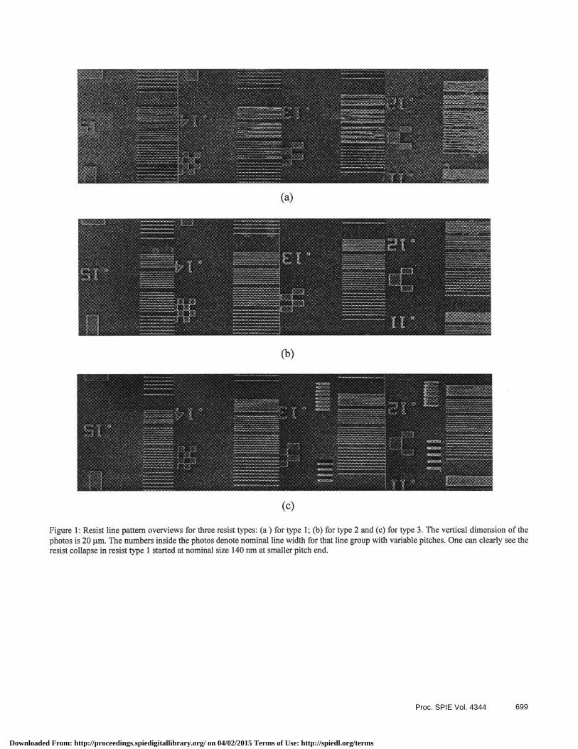
Three different 193 nm resists (resist type I, II and III) from Clariant Corporation were used in this study. Bare silicon waferswere coated with about 450 nm thick resists on top of an organic BARC (Bottom Anti-Reflection Coating) layer. The waferswere exposed using 0.6 NA and 0.7 sigma at a desirable exposure dose for each resist type. Their general behavior is shownin Figure 1 . The lines start to collapse at nominal size 140 nm for resist type I at small pitch end. No resist collapse wasobserved in the other two resist types even down to a nominal size of 120 nm. However, these two types of resists have aslower photospeed (33% more exposure dose is needed to process them). As seen in the inset of Figure 1 (c), the nested linesat a 120 nm nominal size are not fully resolved. In addition, the resist type I exhibits a better profile at 150 nm nominal thanother two resist types (see Figure 2).
Metrology, Inspection, and Process Control for Microlithography XV, Neal T. Sullivan, Editor,Proceedings of SPIE Vol. 4344 (2001) © 2001 SPIE · 0277-786X/01/$15.00 695
Downloaded From: http://proceedings.spiedigitallibrary.org/ on 04/02/2015 Terms of Use: http://spiedl.org/terms
Applied Materials' VeraSEM 3D was used. VeraSEM 3D has an advanced charging control mechanism and is capable ofelectronically tilting the beam up to 5 degrees. Such a capability has proven useful in this study, since it offers the flexibilityto expose only one sidewall of a resist feature to e-beam (see Figure 3).
Both 193 nm resist lines and spaces were measured repeatedly using 500 eV e-beam landing energy and 10 pA beam current,unless otherwise specified. Multiple parameters, e.g., the edge width [6] (single secondary electron peak width), as well asthe top and bottom readings of lines/spaces, can be collected using a unique measurement algorithm. VeraSEM 3D is capableof collecting up to 4 parameters during a single measurement without adding extra time for gathering multiple parameter.
RESULTS AND DISCUSSIONS
1 . Observation of resist shrinkage: the physical resist shrinkage is observable after severe e-beam exposure (continuouse—beam scan for a couple of minutes). Figure 2 shows resist shrinkage for lines and spaces caused by e-beam exposure.By scanning a small area using a tilted beam, we exposed only the top resist side and one sidewall (depending on beamtilting direction) of a line/space, as shown in Figure 3 . This resulted in the resist lines twisting towards the sidewallexposed to e-beam (the twist is more pronounced in the resist type III than in the other two). Such a twist can easily beexplained by vertical shrinkage of one sidewall, while no shrinkage happens to the other side. Thus, by tilting the beam,we not only observed lateral shrinkage, but also vertical shrinkage.
2. Line width shrink versus space growth: Figure 4 shows the comparison of line slimming and space widening of resisttype I as a function of SEM measurement number. The line width shrinks quickly for the first 5repeated measurementsand it then levels off and stays more or less the same after 10 repeated measurements. However, the repeatedmeasurements of a space width show a quick change at the beginning as in a line, then display a near linear trendafterwards (also see Figure 6 b). When measuring a space, more than 5 times more resist is exposed to the e-beam whencompared to a line measurement (for the measurement window width used and the line and space sizes measured in thispaper, also see Figure 2). Thus, for space width measurements, it takes much more e-beam exposure to saturate the resistshrinkage.
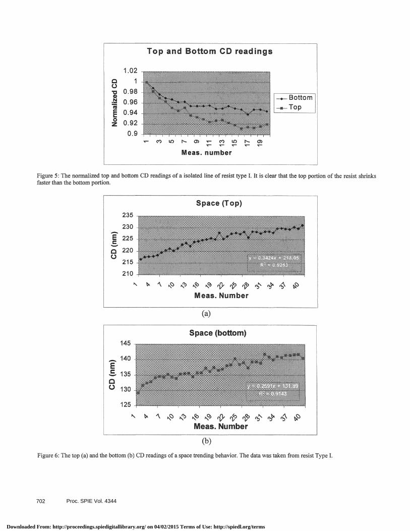
Figure 5 shows the normalized top and bottom CD readings as a function of SEM measurement number. It shows thatthe top portion has a faster shrinking rate than the bottom portion. From Figure 3, one would expect such behavior sincethe top portion of a line/space receives more e-beam exposure than the bottom portion. The SEM measurement of aspace width shows the similar behavior. Figure 6 shows the trending behavior of repeated SEM measurements of boththe top (a) and the bottom (b) CD readings of a space with linear fit. R-square number more than 0.9 shows good lineartrending behavior. The trending slope for the top CD reading is 0.34 nm per measurement, while the trending slope forthe bottom CD reading is 0.26 nm per measurement. Again, it shows that the top of a space opens up faster than thebottom.
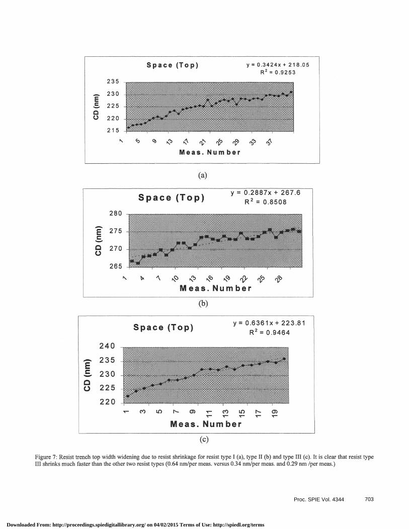
Figure 7 shows a space top width trend for three resist types. The trending slopes indicate the shrinking rate of theresists. It is clear that the resist type III shrinks much faster than the other two resist types (0.64 nm per measurementversus 0.34 and 0.29 nm per measurement), consistent with physical observations in Figure 2. Since thebottom space width trending is subject to an additional variation (sidewall slope angle), the direct comparison ofthe bottom space trending is not as meaningful, if sidewall angles are unknown. To take into account of sidewall angleinfluence, we examine edge width of a space at a tilted view.
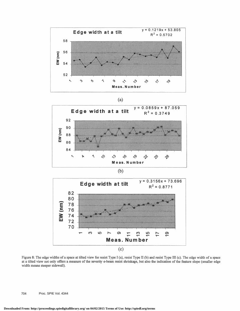
Edge width can be easily measured at a tilted view. Figure 8 shows the repeated SEM measurement results of the edgewidths of spaces for three types of resists. The edge width of a space increases as resist shrinks. The increase of the edgewidth as a function of measurement number is more or less linear. There are two opposite trends influencing an edgewidth of a space at a tilted view: one is a decreasing trend due to resist height shrinkage; while another is an increasingtrend due to the top shrinking faster than the bottom of a space. For a small tilted beam angle (about 5degrees in thisstudy), the resist height shrinkage is independent of space sidewall angle in the first order. However, the shrinking rate ofthe top and bottom space widths depends strongly on space sidewall angles. Sloped sidewalls reduce the edge widthincreasing trend at a tilted view. The edge width for resist type I starts at about 54nm. Using 450 nm resist height andlinear slope approximation, one can estimate the sidewall angle is about 88°. Similarly, one can estimate the spacesidewall angles for resist type II and III as 84° and 86°, respectively. By comparing the edge width trending slope, it isclear that the resist type III shrinks much faster than the other two resist types (0.32 nm/meas. versus 0.12 and 0.09
+ Thee-beam dose is on the order of 0.1 Coulomb/cm2.
Proc. SPIE Vol. 4344696
Downloaded From: http://proceedings.spiedigitallibrary.org/ on 04/02/2015 Terms of Use: http://spiedl.org/terms
nm/meas.). Such a conclusion is consistent with space top measurements. By examining the SEM images in Figure 2,one can reach the same conclusion. Since edge width measurements at a tilted view take into account vertical shrinkage,as well as lateral shrinkage, it could be used as another good indicator for resist shrinkage rate.
The edge width of a line at a tilted view is much more complicated than a space. For a line, there is one more factorthathas to be considered, i.e., the pulling force by one sidewall shrinking at tilted view as seen in Figure 2. Such a forcetwists a line under e-beam irradiation towards the e-beam direction and the system sees less edge width as themeasurements progress. Thus, the trending behavior of an edge width of a line with a tilted view is not as meaningful, ifthe line twist effect under e-beam is unknown.
3. Line edge roughness: There are indications that e-beam induced shrinkage increases line/space edge roughness,especially at the boundary between the resist and BARC as shown in Figure 9. One can see the pronounced spikes in thebottom edge after e-beam exposure. The interaction between the resist shrinkage and the adhesion force at interface maybe the cause of increased line roughness, since the top edge stays smooth. Figure 10 shows the measured line edgeroughness as a function of measurement number. The overall upward trend of line roughness as the measurementprogresses is visible. In addition, on top of the overall upward trending, there are additional up and down peaks. Suchbehavior may suggest that resist shrinkage at the interface of resist and BARC is not continuous, but rather in smallskipping steps. The shrinking force has to overcome adhesion forces at the interface for the resist to move.
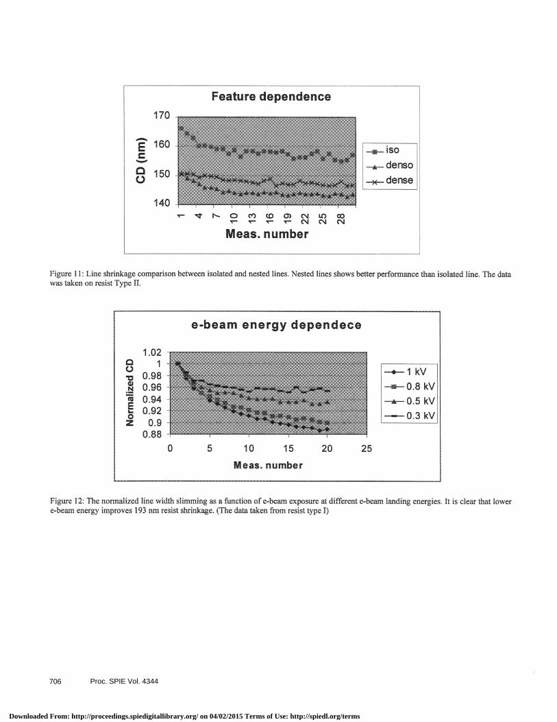
4. Pitch dependence: It appears that the nested lines exhibit a different CD decreasing trend as resists shrink under the e-beam as compared to an isolated line. Figure 1 1 shows CD changes as a function of measurement number for the nestedlines, isolated line and semi-nested lines. The nested lines show a slower rate of CD change as the measurementprogresses, especially at the beginning of the measurements. The data was taken from resist Type II. The other two typesof resists exhibit similar trends between nested and isolated lines. The reason, we believe, is because of the differentsidewall angles between nested and isolated lines. In general, for given lithography conditions, isolated lines have asloped sidewall compared to that of nested lines. Sloped sidewall will increase the e-beam exposed resist volume asshown in Figure 3.
RESIST SHRINKAGE MODEL
Based on the above fmdings, a simple model describing the shrinkage of 1 93 nm resists when irradiated by an electron beamcan be constructed. The cause could be polymer cross-linking or other chemical reactions. We do not quite understand thecause behind the resist shrinkage, but we can still call it cross-linking for the sake of discussion. At low e-beam dose, only asmall percentage of available polymers undergo cross-linking. As the e-beam dose increases as repeated SEM measurementsprogress, polymers undergo cross-linking, until all the available polymers that could be cross linked have undergone cross-linking. The shrink starts within the e-beam penetration depth*. There are two mechanisms that keep the shrinkageprogressing. First, as repeated measurements continue, the increased e-beam dose induces more polymer cross-link within e-beam penetration depth until, it depletes the available cross-links. Second, as the resist shrinks, the e-beam can reach a littlebit deeper into the underlying resist, which will induce more resist shrinkage, until the resist becomes denser (e-beam has lesspenetration depth in dense materials) and prevents the process from going further. The shrinkage will eventually slow down,then stop after enough e-beam exposure.
Let denote AV as the resist volume lost due to e-beam induced resist shrinkage, thenAV = a*Ve(d, D, 0)
where a is a resist dependent number, Ve is the resist volume exposed to e-beam. Ve depends on electron penetration depth(d), the electron exposure dose (D) and the angle (0) that e-beam strikes a sidewall. A tilted beam increases such angle, thus itincreases the shrinking effect through the increased sidewall penetration depth.
Figure 12 shows that lower beam energy improves resist line width shrinkage during SEM CD measurements. For thisparticular resist (resist type I), 20 consecutive SEM CD measurements induces about 5% line width reduction at 300 eV,while at lkeV, such reduction increases to about 11%.
Based on this model, we can make following recommendations to reduce e-beam induced resist shrinkage for a given 193 nmresist:1. Use lower energy electrons to reduce the interaction volume by reducing the e-beam penetration depth.
*The electron beam penetration depth is on the order of 100 nm for photo-resist at 500 eV.
Proc. SPIE Vol. 4344 697
Downloaded From: http://proceedings.spiedigitallibrary.org/ on 04/02/2015 Terms of Use: http://spiedl.org/terms
2. Use lower beam currents and less exposure time to reduce the e-beam dose.3 . Use off-site auto SEM focusing (using a nearby feature to do SEM auto-focus to avoid charging at the site to be
measured—less e-beam dose).4. Improve the resist line profile (near vertical).
Certainly, improving 193 nm resist formulations to minimize e-beam induced shrinkage may prove to be more effective, interms of time to solution and costs.
CONCLUSIONS
We have observed vertical, as well as lateral 193 nm resist shrinkage under e-beam exposure using VeraSEM 3D's uniquesidewall imaging technology. We have characterized different CD changing behaviors for lines, spaces and edge widths.Repeated CD measurements on a space enhance the e-beam induced resist shrinkage effect, due to having more resist volumeexposed to the e-beam during SEM CD measurements. Hence, the resist shrinkage rates of different resists can be directlycompared by measuring their space top widths. The edge widths of spaces at a tilted view offers an indication of both theseverity ofresist shrinkage ofdifferent resist types and the influence ofsidewall slope.
We have also identified critical parameters affecting resist shrinkage in SEM CD measurements. The experimental datashows that the 1 93 urn resists shrinkage is dependent on materials (resist formulation), electron beam energy (throughpenetration), electron dose and feature sidewall angle. A simple physical model describing 193 nm resist shrinkage usingabove parameters is proposed.
REFERENCES
1 . M. Neisser, et al, "Mechanism Studies of Scanning Electron Microscope Measurement Effects on 193 nm Photoresistsand The development of Improved Line Width Measurement Methods", Proc. Interface2000, pp 53 (2000).
2. L. Pain, et al, "Study of 193 nm Resist Behavior under SEM Inspection: How to Reduce Line-width shrinkage Effect?",Proc. Interface2000, pp 233 (2000).
3. B. Su and A. Romana, "Study on 193 nm Photoresist Shrinkage after Electron Beam Exposure", Proc. Interface2000, pp249 (2000).
4. N. R. Bantu, et a!, "Low Shrinkage DUV resist", Proc. Interface'98, pp 229 (1998).5. M. F. Ross, et a!, "Characterization of Electron Beam Stabilization of Deep UV resist", Proc. Interface'97, pp 119
(1997).6. B. Su, et a!, "Sidewall Angle Measurements Using CD-SEM", Proc. Advanced Semiconductor Manufacturing
Conference (ASMC), pp 259-261, (1998).
Proc. SPIE Vol. 4344698
Downloaded From: http://proceedings.spiedigitallibrary.org/ on 04/02/2015 Terms of Use: http://spiedl.org/terms
(a)
(c)
Figure 1: Resist line pnttern overviews for three resist types: (a ) for type I; (b) for type 2 and (c) for type 3. The vertical dimension of thephotos is 20 m. The numbers inside the photos denote nominal line width for that line group with variable pitches. One can clearly see theresist collapse in resist type I started at nominal size 140 rim at smaller pitch end.
(b)
Proc. SPIE Vol. 4344 699
Downloaded From: http://proceedings.spiedigitallibrary.org/ on 04/02/2015 Terms of Use: http://spiedl.org/terms

Figure 2: The lines (the left side photos) become smaller and the spaces (the right side photos) become larger after severe ebeam exposureat a tilted angle (5 degrees). All six photos are taken at a tilted angle at 2 mFOV,
Type I resist
Type II resist
Type III resist
Proc. SPIE Vol. 4344700
Downloaded From: http://proceedings.spiedigitallibrary.org/ on 04/02/2015 Terms of Use: http://spiedl.org/terms

Figure 3: illustrations of the differences between a top down scan and a tilted scan for a line and a space. Note the penetration depthincrease at a sidewall due to beam tilt,
Figure 4: Line slimming and space widening due to resist shrinkage under e-beam exposure. The line width stays more or less the sameafter 10 measurements, while the space width keeps widening even after 30 measurements. (resist type 1)
(a) (c)
(b) (d)
Line shrinkage and space widening
I 50
145
140C
135
U 130125
120
—.—Line
-*— Space
o c c, tc%
Meas. number
Proc. SPIE Vol. 4344 701
Downloaded From: http://proceedings.spiedigitallibrary.org/ on 04/02/2015 Terms of Use: http://spiedl.org/terms
Top and Bottom CD readings
Figure 5: The normalized top and bottom CD readings of a isolated line of resist type I. It is clear that the top portion of the resist shrinksfaster than the bottom portion.
(a)
(b)
Figure 6: The top (a) and the bottom (b) CD readings ofa space trending behavior. The data was taken from resist Type I.
1.02I00
wN
E0z
0.98
0.960.940.92
om0.9 c ' i 0 LO 0)-
Meas. number
Space (Top)235
230
225
22040215 4
210
Meas. Number
Space (bottom)I 45
140EC
0 130
I 25
\Meas. Number
Proc. SPIE Vol. 4344702
Downloaded From: http://proceedings.spiedigitallibrary.org/ on 04/02/2015 Terms of Use: http://spiedl.org/terms
(a)
(b)
(c)
Figure 7: Resist trench top width widening due to resist shrinkage for resist type I (a), type II (b) and type III (c). It is clear that resist typeIII shrinks much faster than the other two resist types (064 nm/per meas. versus 0.34 nm/per meas. and 0.29 am /per meas.)
Space (Top) y — Oi4z4x + 218.05R1 0.9L53
235
230 . . .E'B- 225 • . .. . > .
00 220 . ' , ' '., . . , ..
215p\ D b r (tD qb e 4'
Meas. Num ber
Space (Top)280
y = O.2887x + 267.6R2 0.8508
I 275 HC
§' 270
265 -\
Meas. Number
Space (Top)
240I
y= 0.6361x+ 223.81R2 0.9464
U 225220
t . .. . . . , . ? . . _ .. . . ,_ . . .. . — ..
r LU
I -r r tO LU F Or r r rMeas Number
Proc. SPIE Vol. 4344 703
Downloaded From: http://proceedings.spiedigitallibrary.org/ on 04/02/2015 Terms of Use: http://spiedl.org/terms
(a)
(b)
(c)
Figure 8: The edge widths of a space at tilted view for resist Type I (a), resist Type II (b) and resist Type III (c). The edge width of a spaceat a tilted view not only offers a measure of the severity ebeam resist shrinkage, but also the indication of the feature slope (smaller edgewidth means steeper sidewall).
Edge width at a tilt58
56EC
w
y = O1219x + 53.805R2 0.5702
54 452
\ 1 % \\Meas. Number
t
Edge width at a tilt92 -
90
88
y = 0.0859x + 87.059R2 03749
EC
w 86
84 -N k $ .
Meas. Number
Edge width at tilt828078I
C
y= O.3156x+ 73.696R2 0.8771
76
w7472
.
70 r N r tOr r rMeas. Number
Nr
Proc. SPIE Vol. 4344704
Downloaded From: http://proceedings.spiedigitallibrary.org/ on 04/02/2015 Terms of Use: http://spiedl.org/terms
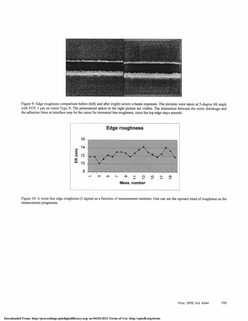
Figure 9: Edge roughness comparison before (left) and after (right) severe e-beam exposure. The pictures were taken at 5-degree tilt anglewith FOV 1 jun on resist Type II. The pronounced spikes in the right picture are visible. The interaction between the resist shrinkage andthe adhesion force at interface may be the cause for increased line roughness, since the top edge stays smooth.
Figure 10: A resist line edge roughness (3 sigma) as a function ofmeasurement numbers. One can see the upward trend ofroughness as themeasurement progresses.
Edge roughness
L() N. C) — C') LC) N- C)
Meas, number
Proc. SPIE Vol. 4344 705
Downloaded From: http://proceedings.spiedigitallibrary.org/ on 04/02/2015 Terms of Use: http://spiedl.org/terms
Feature dependence
Figure 1 1 : Line shrinkage comparison between isolated and nested lines. Nested lines shows better performance than isolated line. The datawas taken on resist Type II.
0.940.920.9
Figure 12: The nomialized line width slimming as a function ofe-beam exposure at different e-beam landing energies. It is clear that lowere-beam energy improves 193 mu resist shrinkage. (The data taken from resist Wpe I)
I 70
? 160C
C 150aI 40
—A— denso
r F 0 0 O'J 00r r r r N 1 iMeas. number
ebeam energy dependece
1.02C I "C)V 0.980)Nc •
E0z • . ."-..
0 5 10 15 20 25
Meas number
0.88
Proc. SPIE Vol. 4344706
Downloaded From: http://proceedings.spiedigitallibrary.org/ on 04/02/2015 Terms of Use: http://spiedl.org/terms


![Page 34 of 193 (Objection [India]](https://img.dokumen.tips/doc/110x75/6331c2555696ca447302e632/page-34-of-193-objection-india.jpg)


