Embed Size (px)
Citation preview
11 Concurrent Code: Practice
This chapter is a continuation of chapter 10. Both deal with purely concurrent (i.e., without pro cess) VHDL code, which is appropriate for implementing only combinational cir cuits. While the previous chapter was dedicated to more conceptual aspects (nevertheless with practical examples included), the pre sent chapter is dedicated entirely to practice with con-current code, including additional design examples and a list of select exercises.
The list of all enumerated examples and exercises in this edition of the book is in appen-dix M.
11.1 Additional Design Examples Using Concurrent Code
The following design examples using purely concurrent code are presented in this chapter:
Example 11.1. Vectors absolute difference calculator
Example 11.2. Programmable combinational delay line (structural)
Example 11.3. Sine calculator with integers and ROM- type memory
Example 11.1. Vectors absolute difference calculatorThis example deals with a cir cuit that must calculate, in parallel and with minimum time complexity, the accumulated absolute difference abs_diff = Σ|ak − bk| between vectors a and b, where each vector contains M = 8 ele ments, the ele ments being N- bit signed integers (con-trary to M, the pa ram e ter N is generic). Since this is an arithmetic cir cuit (sign matters), the suggestions presented in section 10.7 will be taken into consideration.
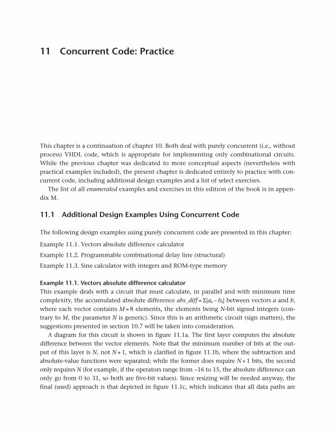
A diagram for this cir cuit is shown in figure 11.1a. The first layer computes the absolute difference between the vector ele ments. Note that the minimum number of bits at the out-put of this layer is N, not N + 1, which is clarified in figure 11.1b, where the subtraction and absolute- value functions were separated; while the former does require N + 1 bits, the second only requires N (for example, if the operators range from −16 to 15, the absolute difference can only go from 0 to 31, so both are five- bit values). Since resizing will be needed anyway, the final (used) approach is that depicted in figure 11.1c, which indicates that all data paths are
266 Chapter 11
resized to N + 3 bits (not N + 4). The remaining layers implement an adder array. Because mini-mum time complexity is required, the tree- type structure (figure 1.15b) was chosen, so the time complexity is O(L + 1), where L = ⎡log2M⎤ (=3 for M = 8) is the number of layers in the adder tree.
This is an arithmetic cir cuit that employs integers, so according to section 10.7, the right “arithmetic” type is unsigned or signed. In fact, both are needed in this example: signed for the first layer ( because the vector ele ments can be negative) and unsigned after the absolute- value function. We must next check the constraints on the involved operators for these specific data types; table 9.4 shows that the “+” and “−” operators require the result to have the same number of bits as the largest operand, while the abs operator requires the output to have the size of the input. So now we fi nally have all information needed to develop a corresponding VHDL code.
A solution for this prob lem is presented next. Because an array of signed values is needed (to represent the vectors) at the cir cuit ports, and this kind of type is not available among the predefined types, it must be created in a package (the construction of packages is described in chapter 14), shown in the first code below. The package is called user_defined_type_pkg and the user- defined type is called signed_array, its individual ele ments being of type signed. Note that this package is listed in line 4 of the second code.
The design code is called abs_difference_calculator (line 6). The entity declaration (lines 6–12) starts with N being declared as a generic pa ram e ter (according with section 5.8.3, a better name would be NUM_BITS or WIDTH, for example; name N was kept just to match figure 11.1). Next come the cir cuit ports, where a and b are of type signed_array and the output is of type unsigned (with N + 3 bits).
The architecture body (lines 14–29), containing only purely concurrent code (no pro cesses), has its statement region divided in two parts. The first (lines 20–22) implements the first layer of figure 11.1a, using the resize function (section 7.9.3) followed by subtraction, then the abs operator, and fi nally conversion to unsigned using type cast (section 7.10.2). The second part (lines 25–28) implements the adder array; because M is neither generic nor large, the tree was constructed explic itly (proper use of parentheses suffice to obtain the tree- type structure).
Figure 11.1Accumulated absolute difference calculator of example 11.1.
Concurrent Code: Practice 267
For fully generic trees, the use of sequential (instead of concurrent) code leads to simpler solutions, as illustrated in chapter 13 (example 13.1).
1 ------------------------------------------------------------------ 2 library ieee; 3 use ieee.numeric_std.all; 4 package user_defined_type_pkg is 5 type signed_array is array (natu ral range <>) of signed; 6 end package; 7 ------------------------------------------------------------------
1 -------------------------------------------------------------------------------------- 2 library ieee; 3 use ieee.numeric_std.all; 4 use work . user _ defined _ type _ pkg . all; 5 6 entity abs_difference_calculator is 7 generic ( 8 N: natu ral := 7); --number of bits in input ele ments 9 port ( 10 a, b: in signed_array(0 to 7)(N-1 downto 0); 11 abs_difference: out unsigned(N+2 downto 0)); 12 end entity; 13 14 architecture tree_type_nongeneric of abs_difference_calculator is 15 type unsigned_array is array (natu ral range <>) of unsigned; 16 signal abs_diff_vector: unsigned_array(0 to 7)(N+2 downto 0); 17 begin 18 19 --Absolute-differences calculator: 20 gen_diff_vec: for i in 0 to 7 generate 21 abs_diff_vector(i) <= unsigned(abs(resize(a(i), N+3) - resize(b(i), N+3))); 22 end generate; 23 24 --Adder array: 25 abs_difference <= ((abs_diff_vector(0) + abs_diff_vector(1)) + 26 (abs_diff_vector(2) + abs_diff_vector(3))) + 27 ((abs_diff_vector(4) + abs_diff_vector(5)) + 28 (abs_diff_vector(6) + abs_diff_vector(7))); 29 end architecture; 30 --------------------------------------------------------------------------------------
268 Chapter 11
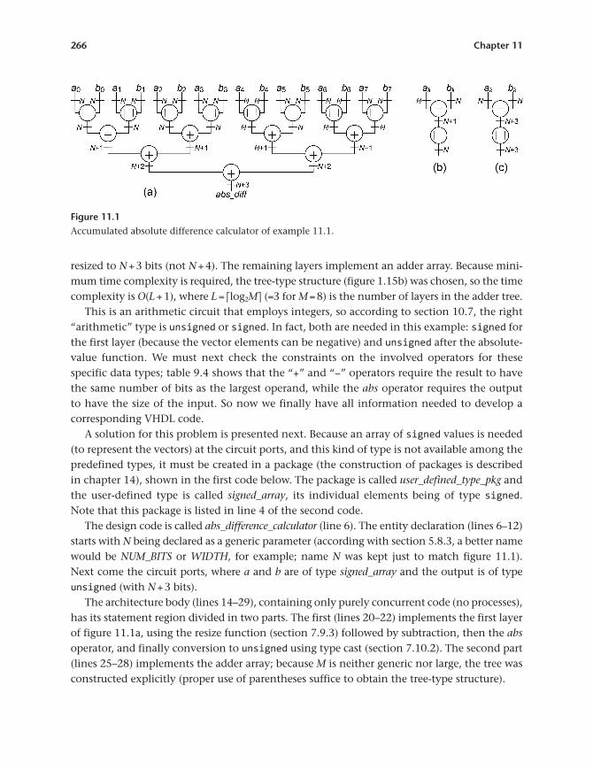
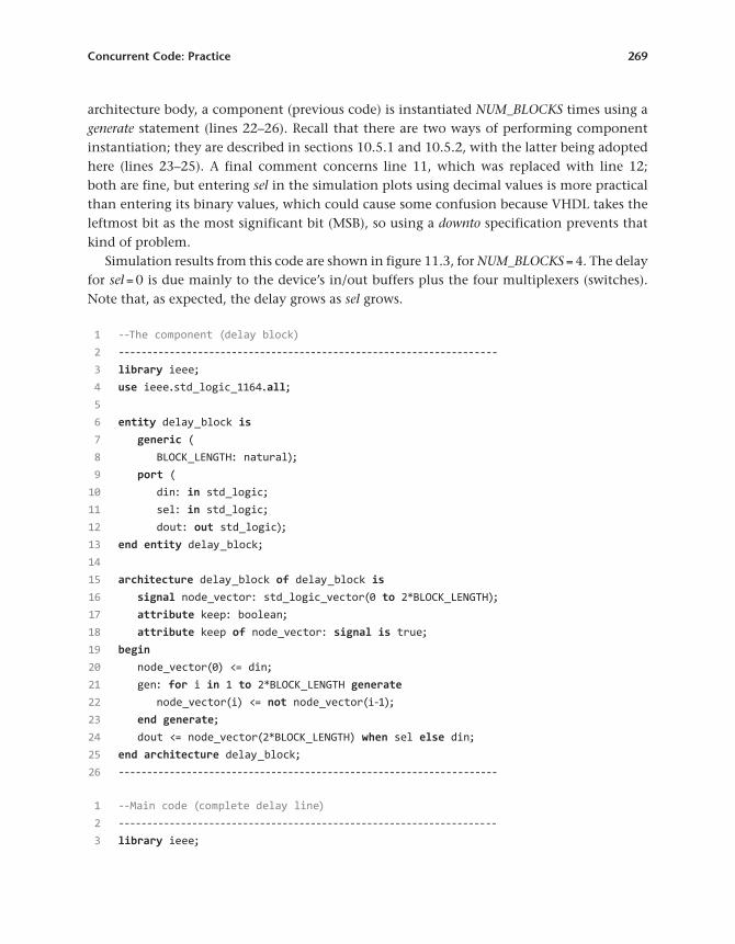
Example 11.2. Programmable combinational delay line (structural)Tapped delay lines, described in section 2.6.9, are sequential cir cuits. The delay line treated here is their combinational counterpart (no clock involved). This kind of cir cuit is used, for example, in the construction of digital delay locked loop (DLL) cir cuits. This example offers a great opportunity for practicing with structural code (code that employs component instan-tiation) with complex structure ( because the size of the cir cuit is generic and the sizes of its building blocks are not constant).
Figure 11.2a shows the cir cuit ports, where din is the (single- bit) signal to be delayed, sel is a control signal that selects the amount of delay, and dout is the delayed version of din. As shown in figure 11.2b, the size of each block is a power of two and the total number of blocks is M, hence producing a delay line that can operate with any number of delay units between 0 and 2M − 1 (a delay unit is a pair of inverters, as indicated in block 1).
Note: In ASICs, the switches of figure 11.2b are usually built with transmission gates (seen in figure 1.1), which exhibit very small propagation delay. If synthesized in an FPGA, the switches will likely be implemented as multiplexers (figure 11.2c), thus with non- negligible propagation delay (illustrated in the timing simulation ahead).
A solution for this prob lem is presented below using a structural approach. The first code is for a single block (called delay_block, line 6). It has a generic size (called BLOCK_LENGTH, line 8), whose value does not need to be specified here because that will be done during instantiation by the generic map association. All ports (lines 10–12) employ a standard- logic type. In the declarative part of the architecture body (lines 16–18), a signal called node_vec-tor is created to represent the internal nodes, to which the keep attribute (section 9.5.3) is applied subsequently. Fi nally, in the statements part of the architecture body (lines 20–24), a generate statement (lines 21–23) is used to build a delay block with a total of BLOCK_LENGTH pairs of inverters. Note that the switch (mux) is implemented by a when statement (line 24).
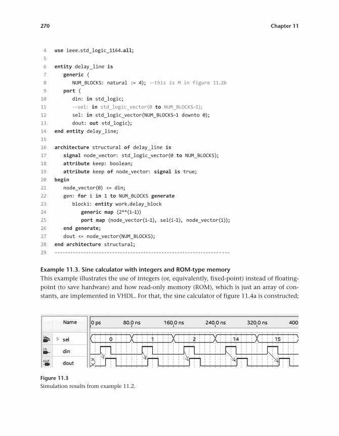
The main code is called delay line (line 6 of the second code below). Note that M (called NUM_BLOCKS in the code, line 8) is a generic pa ram e ter and all ports (lines 10–13) employ again standard- logic types. In the declarative part of the architecture (lines 17–19), a signal is again created to represent the internal cir cuit nodes, to which the keep attribute is applied subsequently. Note that employing signal names already used in the previous code is fine because the codes are interpreted in de pen dently. In the statements part (lines 21–27) of the
Figure 11.2Programmable combinational delay line of example 11.2.
Concurrent Code: Practice 269
architecture body, a component (previous code) is instantiated NUM_BLOCKS times using a generate statement (lines 22–26). Recall that there are two ways of performing component instantiation; they are described in sections 10.5.1 and 10.5.2, with the latter being adopted here (lines 23–25). A final comment concerns line 11, which was replaced with line 12; both are fine, but entering sel in the simulation plots using decimal values is more practical than entering its binary values, which could cause some confusion because VHDL takes the leftmost bit as the most significant bit (MSB), so using a downto specification prevents that kind of prob lem.
Simulation results from this code are shown in figure 11.3, for NUM_BLOCKS = 4. The delay for sel = 0 is due mainly to the device’s in/out buffers plus the four multiplexers (switches). Note that, as expected, the delay grows as sel grows.
1 --The component (delay block) 2 ------------------------------------------------------------------- 3 library ieee; 4 use ieee.std_logic_1164.all; 5 6 entity delay_block is 7 generic ( 8 BLOCK_LENGTH: natu ral); 9 port ( 10 din: in std_logic; 11 sel: in std_logic; 12 dout: out std_logic); 13 end entity delay_block; 14 15 architecture delay_block of delay_block is 16 signal node_vector: std_logic_vector(0 to 2*BLOCK_LENGTH); 17 attribute keep: boolean; 18 attribute keep of node_vector: signal is true; 19 begin 20 node_vector(0) <= din; 21 gen: for i in 1 to 2*BLOCK_LENGTH generate 22 node_vector(i) <= not node_vector(i-1); 23 end generate; 24 dout <= node_vector(2*BLOCK_LENGTH) when sel else din; 25 end architecture delay_block; 26 -------------------------------------------------------------------
1 --Main code (complete delay line) 2 ------------------------------------------------------------------- 3 library ieee;
270 Chapter 11
4 use ieee.std_logic_1164.all; 5 6 entity delay_line is 7 generic ( 8 NUM_BLOCKS: natu ral := 4); --this is M in figure 11.2b 9 port ( 10 din: in std_logic; 11 --sel: in std_logic_vector(0 to NUM_BLOCKS-1); 12 sel: in std_logic_vector(NUM_BLOCKS-1 downto 0); 13 dout: out std_logic); 14 end entity delay_line; 15 16 architecture structural of delay_line is 17 signal node_vector: std_logic_vector(0 to NUM_BLOCKS); 18 attribute keep: boolean; 19 attribute keep of node_vector: signal is true; 20 begin 21 node_vector(0) <= din; 22 gen: for i in 1 to NUM_BLOCKS generate 23 blocki: entity work.delay_block 24 generic map (2**(i-1)) 25 port map (node_vector(i-1), sel(i-1), node_vector(i)); 26 end generate; 27 dout <= node_vector(NUM_BLOCKS); 28 end architecture structural; 29 -------------------------------------------------------------------
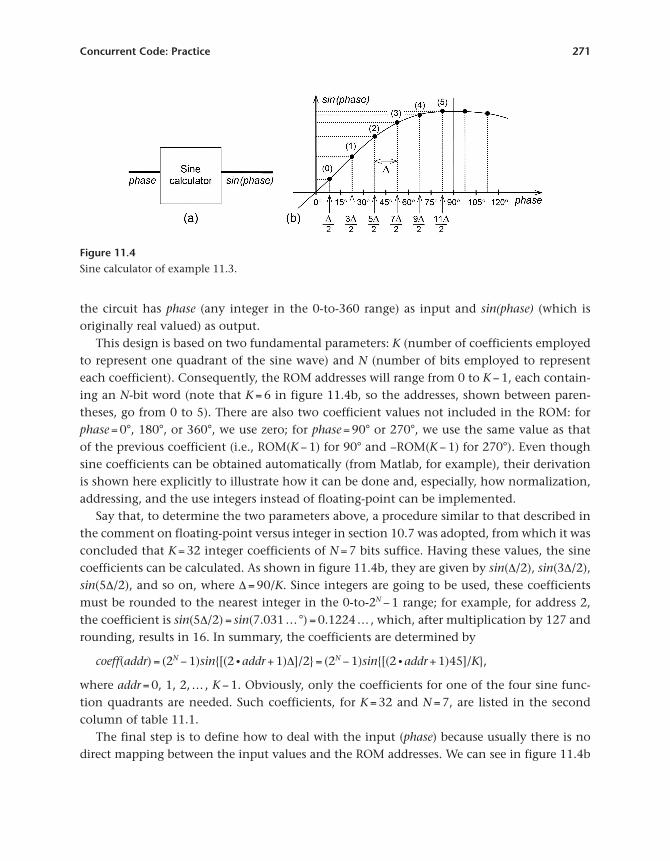
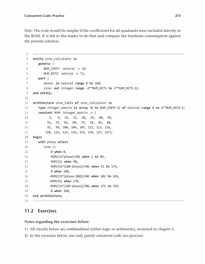
Example 11.3. Sine calculator with integers and ROM- type memoryThis example illustrates the use of integers (or, equivalently, fixed-point) instead of floating-point (to save hardware) and how read- only memory (ROM), which is just an array of con-stants, are implemented in VHDL. For that, the sine calculator of figure 11.4a is constructed;
Figure 11.3Simulation results from example 11.2.
Concurrent Code: Practice 271
the cir cuit has phase (any integer in the 0- to-360 range) as input and sin(phase) (which is originally real valued) as output.
This design is based on two fundamental par ameters: K (number of coefficients employed to represent one quadrant of the sine wave) and N (number of bits employed to represent each coefficient). Consequently, the ROM addresses will range from 0 to K − 1, each contain-ing an N- bit word (note that K = 6 in figure 11.4b, so the addresses, shown between paren-theses, go from 0 to 5). There are also two coefficient values not included in the ROM: for phase = 0°, 180°, or 360°, we use zero; for phase = 90° or 270°, we use the same value as that of the previous coefficient (i.e., ROM(K − 1) for 90° and −ROM(K − 1) for 270°). Even though sine coefficients can be obtained automatically (from Matlab, for example), their derivation is shown here explic itly to illustrate how it can be done and, especially, how normalization, addressing, and the use integers instead of floating-point can be implemented.
Say that, to determine the two par ameters above, a procedure similar to that described in the comment on floating-point versus integer in section 10.7 was adopted, from which it was concluded that K = 32 integer coefficients of N = 7 bits suffice. Having these values, the sine coefficients can be calculated. As shown in figure 11.4b, they are given by sin(Δ/2), sin(3Δ/2), sin(5Δ/2), and so on, where Δ = 90/K. Since integers are going to be used, these coefficients must be rounded to the nearest integer in the 0- to-2N − 1 range; for example, for address 2, the coefficient is sin(5Δ/2) = sin(7.031 … °) = 0.1224 … , which, after multiplication by 127 and rounding, results in 16. In summary, the coefficients are determined by
coeff(addr) = (2N − 1)sin{[(2 addr + 1)Δ]/2} = (2N − 1)sin{[(2 addr + 1)45]/K},
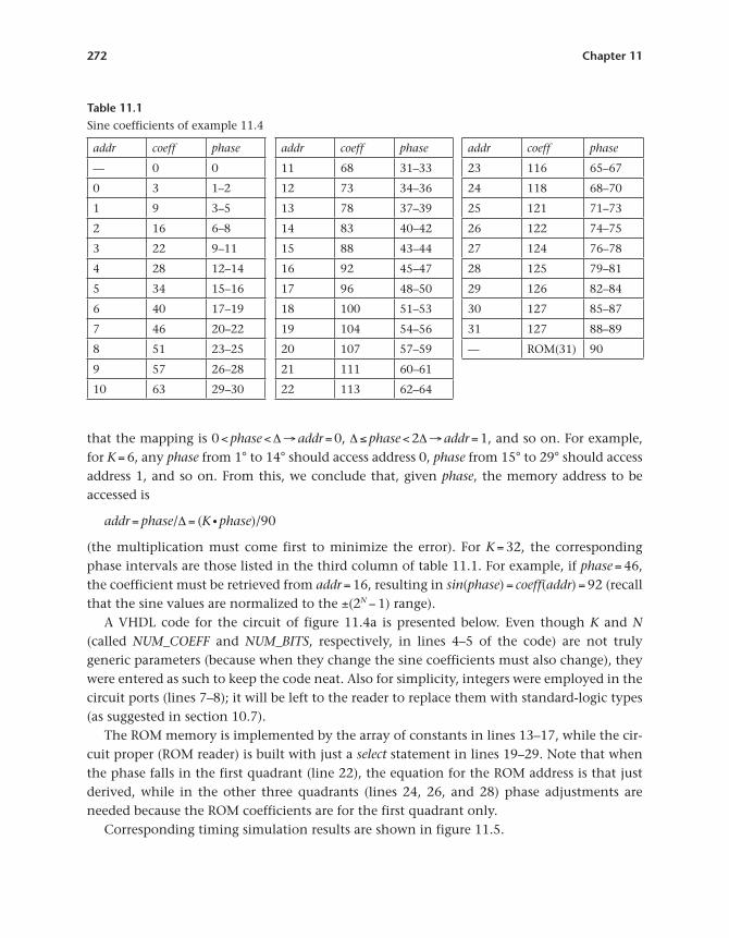
where addr = 0, 1, 2, … , K − 1. Obviously, only the coefficients for one of the four sine func-tion quadrants are needed. Such coefficients, for K = 32 and N = 7, are listed in the second column of table 11.1.
The final step is to define how to deal with the input (phase) because usually there is no direct mapping between the input values and the ROM addresses. We can see in figure 11.4b
Figure 11.4Sine calculator of example 11.3.
272 Chapter 11
that the mapping is 0 < phase < Δ → addr = 0, Δ ≤ phase < 2Δ → addr = 1, and so on. For example, for K = 6, any phase from 1° to 14° should access address 0, phase from 15° to 29° should access address 1, and so on. From this, we conclude that, given phase, the memory address to be accessed is
addr = phase/Δ = (K phase)/90
(the multiplication must come first to minimize the error). For K = 32, the corresponding phase intervals are those listed in the third column of table 11.1. For example, if phase = 46, the coefficient must be retrieved from addr = 16, resulting in sin(phase) = coeff(addr) = 92 (recall that the sine values are normalized to the ±(2N − 1) range).
A VHDL code for the cir cuit of figure 11.4a is presented below. Even though K and N (called NUM_COEFF and NUM_BITS, respectively, in lines 4–5 of the code) are not truly generic par ameters ( because when they change the sine coefficients must also change), they were entered as such to keep the code neat. Also for simplicity, integers were employed in the cir cuit ports (lines 7–8); it will be left to the reader to replace them with standard- logic types (as suggested in section 10.7).
The ROM memory is implemented by the array of constants in lines 13–17, while the cir-cuit proper (ROM reader) is built with just a select statement in lines 19–29. Note that when the phase falls in the first quadrant (line 22), the equation for the ROM address is that just derived, while in the other three quadrants (lines 24, 26, and 28) phase adjustments are needed because the ROM coefficients are for the first quadrant only.
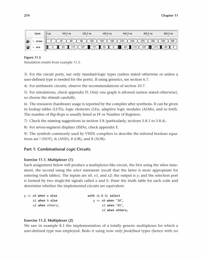
Corresponding timing simulation results are shown in figure 11.5.
Table 11.1Sine coefficients of example 11.4
addr coeff phase addr coeff phase addr coeff phase
— 0 0 11 68 31–33 23 116 65–67
0 3 1–2 12 73 34–36 24 118 68–70
1 9 3–5 13 78 37–39 25 121 71–73
2 16 6–8 14 83 40–42 26 122 74–75
3 22 9–11 15 88 43–44 27 124 76–78
4 28 12–14 16 92 45–47 28 125 79–81
5 34 15–16 17 96 48–50 29 126 82–84
6 40 17–19 18 100 51–53 30 127 85–87
7 46 20–22 19 104 54–56 31 127 88–89
8 51 23–25 20 107 57–59 — ROM(31) 90
9 57 26–28 21 111 60–61
10 63 29–30 22 113 62–64
Concurrent Code: Practice 273
1 ------------------------------------------------------------------------------------------------ 2 entity sine_calculator is 3 generic ( 4 NUM_COEFF: natu ral := 32; 5 NUM_BITS: natu ral := 7); 6 port ( 7 phase: in natu ral range 0 to 360; 8 sine: out integer range -2**NUM_BITS to 2**NUM_BITS-1); 9 end entity; 10 11 architecture sine_table of sine_calculator is 12 type integer_matrix is array (0 to NUM_COEFF-1) of natu ral range 0 to 2**NUM_BITS-1; 13 constant ROM: integer_matrix := ( 14 3, 9, 16, 22, 28, 34, 40, 46, 15 51, 57, 63, 68, 73, 78, 83, 88, 16 92, 96, 100, 104, 107, 111, 113, 116, 17 118, 121, 122, 124, 125, 126, 127, 127); 18 begin 19 with phase select 20 sine <= 21 0 when 0, 22 ROM((32*phase)/90) when 1 to 89, 23 ROM(31) when 90, 24 ROM((32*(180-phase))/90) when 91 to 179, 25 0 when 180, 26 -ROM((32*(phase-180))/90) when 181 to 269, 27 -ROM(31) when 270, 28 -ROM((32*(360-phase))/90) when 271 to 359, 29 0 when 360; 30 end architecture; 31 ------------------------------------------------------------------------------------------------
11.2 Exercises
Notes regarding the exercises below:
1) All cir cuits below are combinational ( either logic or arithmetic), reviewed in chapter 1.
2) In the exercises below, use only purely concurrent code (no pro cess).
Note: The code would be simpler if the coefficients for all quadrants were included directly in the ROM. It is left to the reader to do that and compare the hardware consumption against the present solution.
274 Chapter 11
3) For the cir cuit ports, use only standard- logic types ( unless stated other wise or unless a user- defined type is needed for the ports). If using generics, see section 6.7.
4) For arithmetic cir cuits, observe the recommendations of section 10.7.
5) For simulations, check appendix D. Only one graph is allowed ( unless stated other wise), so choose the stimuli carefully.
6) The resources (hardware) usage is reported by the compiler after synthesis. It can be given in lookup tables (LUTs), logic ele ments (LEs), adaptive logic modules (ALMs), and so forth. The number of flip- flops is usually listed as FF or Number of Registers.
7) Check the naming suggestions in section 5.8 (particularly, sections 5.8.1 to 5.8.4).
8) For seven- segment displays (SSDs), check appendix E.
9) The symbols commonly used by VHDL compilers to describe the inferred boolean equa-tions are ! (NOT), & (AND), # (OR), and $ (XOR).
Part 1: Combinational Logic Cir cuits
Exercise 11.1. Multiplexer (1)Each assignment below will produce a multiplexer- like cir cuit, the first using the when state-ment, the second using the select statement (recall that the latter is more appropriate for entering truth tables). The inputs are x0, x1, and x2; the output is y; and the se lection port is formed by two single- bit signals called a and b. Draw the truth table for each code and determine whether the implemented cir cuits are equivalent.
y <= x0 when a else with (a & b) select x1 when b else y <= x0 when "10", x2 when others; x1 when "01", x2 when others;
Exercise 11.2. Multiplexer (2)We saw in example 8.1 the implementation of a totally generic multiplexer for which a user- defined type was employed. Redo it using now only predefined types (hence with no
Figure 11.5Simulation results from example 11.3.
Concurrent Code: Practice 275
need for a user- defined package). More specifically, use only standard- logic types for the cir cuit ports. Enter NUM_INPUTS and NUM_BITS as generic constants. (Hint: Sections 7.6.6 and 7.10.3.)
Exercise 11.3. Address decoderAddress decoders were reviewed in section 1.4.2.
a) Why are they said to be combinational?
b) Write a VHDL code that implements the cir cuit of figure 1.4. Enter the number of bits at the input (call it NUM_BITS) as a generic pa ram e ter. Observe notes 2 and 3 above. (Hint: Section 7.10.3.)
c) Show simulation results, for NUM_BITS = 3. Observe note 5 above.
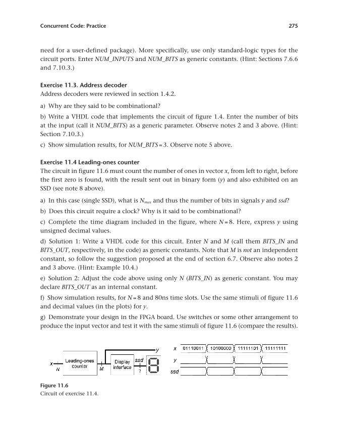
Exercise 11.4 Leading- ones counterThe cir cuit in figure 11.6 must count the number of ones in vector x, from left to right, before the first zero is found, with the result sent out in binary form (y) and also exhibited on an SSD (see note 8 above).
a) In this case (single SSD), what is Nmax and thus the number of bits in signals y and ssd?
b) Does this circuit require a clock? Why is it said to be combinational?
c) Complete the time diagram included in the figure, where N = 8. Here, express y using unsigned decimal values.
d) Solution 1: Write a VHDL code for this cir cuit. Enter N and M (call them BITS_IN and BITS_OUT, respectively, in the code) as generic constants. Note that M is not an in de pen dent constant, so follow the suggestion proposed at the end of section 6.7. Observe also notes 2 and 3 above. (Hint: Example 10.4.)
e) Solution 2: Adjust the code above using only N (BITS_IN) as generic constant. You may declare BITS_OUT as an internal constant.
f) Show simulation results, for N = 8 and 80ns time slots. Use the same stimuli of figure 11.6 and decimal values (in the plots) for y.
g) Demonstrate your design in the FPGA board. Use switches or some other arrangement to produce the input vector and test it with the same stimuli of figure 11.6 (compare the results).
Figure 11.6Cir cuit of exercise 11.4.
276 Chapter 11
Exercise 11.5. Largest cluster of onesAssume now that the cir cuit of figure 11.6 must inform the size of the largest group of con-secutive ones instead of informing the number of leading ones; for example, if the input is x = "0011010111100", the output has to be y = 4. Solve all parts (a to g) of exercise 11.4 for this new circuit.
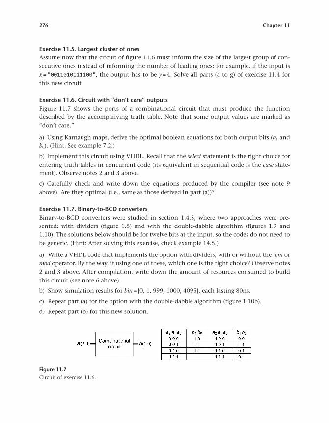
Exercise 11.6. Cir cuit with “ don’t care” outputsFigure 11.7 shows the ports of a combinational cir cuit that must produce the function described by the accompanying truth table. Note that some output values are marked as “ don’t care.”
a) Using Karnaugh maps, derive the optimal boolean equations for both output bits (b1 and b0). (Hint: See example 7.2.)
b) Implement this cir cuit using VHDL. Recall that the select statement is the right choice for entering truth tables in concurrent code (its equivalent in sequential code is the case state-ment). Observe notes 2 and 3 above.
c) Carefully check and write down the equations produced by the compiler (see note 9 above). Are they optimal (i.e., same as those derived in part (a))?
Exercise 11.7. Binary- to- BCD convertersBinary- to- BCD converters were studied in section 1.4.5, where two approaches were pre-sented: with dividers (figure 1.8) and with the double- dabble algorithm (figures 1.9 and 1.10). The solutions below should be for twelve bits at the input, so the codes do not need to be generic. (Hint: After solving this exercise, check example 14.5.)
a) Write a VHDL code that implements the option with dividers, with or without the rem or mod operator. By the way, if using one of these, which one is the right choice? Observe notes 2 and 3 above. After compilation, write down the amount of resources consumed to build this cir cuit (see note 6 above).
b) Show simulation results for bin = {0, 1, 999, 1000, 4095}, each lasting 80ns.
c) Repeat part (a) for the option with the double- dabble algorithm (figure 1.10b).
d) Repeat part (b) for this new solution.
Figure 11.7Cir cuit of exercise 11.6.
Concurrent Code: Practice 277
e) Compare the resources usage of the two solutions above.
f) Demonstrate your design from part (c) in the FPGA board. Explain how you are going to produce the input signal.
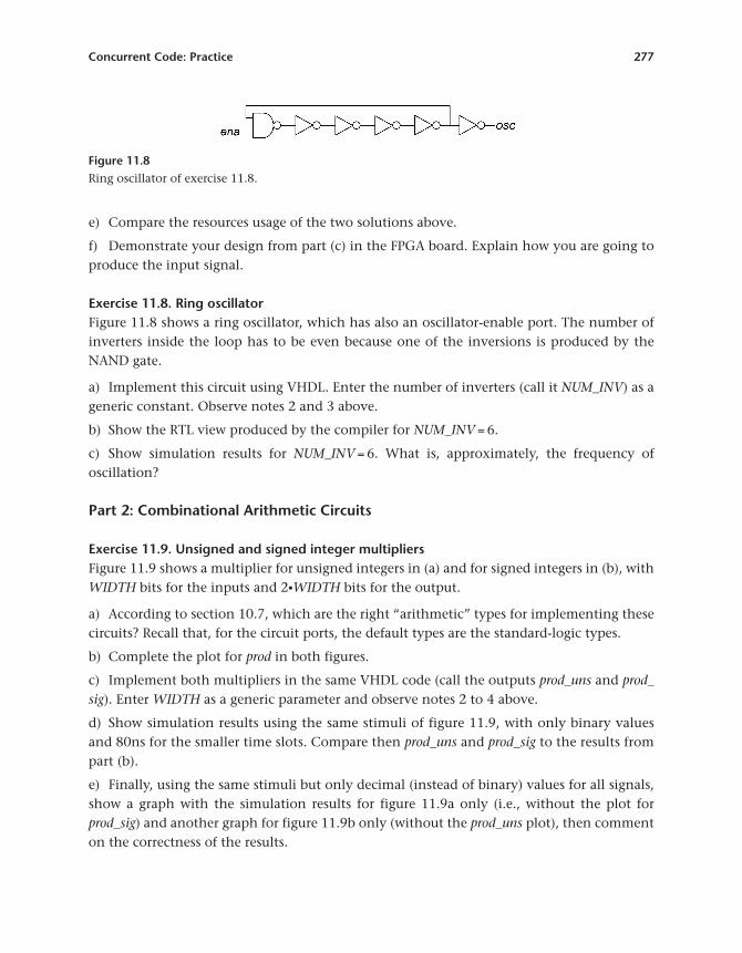
Exercise 11.8. Ring oscillatorFigure 11.8 shows a ring oscillator, which has also an oscillator- enable port. The number of inverters inside the loop has to be even because one of the inversions is produced by the NAND gate.
a) Implement this cir cuit using VHDL. Enter the number of inverters (call it NUM_INV) as a generic constant. Observe notes 2 and 3 above.
b) Show the RTL view produced by the compiler for NUM_INV = 6.
c) Show simulation results for NUM_INV = 6. What is, approximately, the frequency of oscillation?
Part 2: Combinational Arithmetic Cir cuits
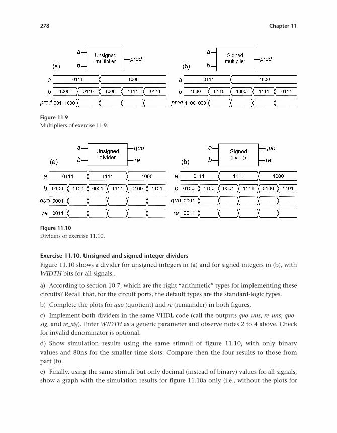
Exercise 11.9. Unsigned and signed integer multipliersFigure 11.9 shows a multiplier for unsigned integers in (a) and for signed integers in (b), with WIDTH bits for the inputs and 2WIDTH bits for the output.
a) According to section 10.7, which are the right “arithmetic” types for implementing these cir cuits? Recall that, for the cir cuit ports, the default types are the standard- logic types.
b) Complete the plot for prod in both figures.
c) Implement both multipliers in the same VHDL code (call the outputs prod_uns and prod_sig). Enter WIDTH as a generic pa ram e ter and observe notes 2 to 4 above.
d) Show simulation results using the same stimuli of figure 11.9, with only binary values and 80ns for the smaller time slots. Compare then prod_uns and prod_sig to the results from part (b).
e) Fi nally, using the same stimuli but only decimal (instead of binary) values for all signals, show a graph with the simulation results for figure 11.9a only (i.e., without the plot for prod_sig) and another graph for figure 11.9b only (without the prod_uns plot), then comment on the correctness of the results.
Figure 11.8Ring oscillator of exercise 11.8.
278 Chapter 11
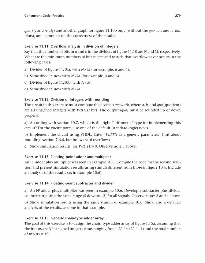
Exercise 11.10. Unsigned and signed integer dividersFigure 11.10 shows a divider for unsigned integers in (a) and for signed integers in (b), with WIDTH bits for all signals..
a) According to section 10.7, which are the right “arithmetic” types for implementing these cir cuits? Recall that, for the cir cuit ports, the default types are the standard- logic types.
b) Complete the plots for quo (quotient) and re (remainder) in both figures.
c) Implement both dividers in the same VHDL code (call the outputs quo_uns, re_uns, quo_sig, and re_sig). Enter WIDTH as a generic pa ram e ter and observe notes 2 to 4 above. Check for invalid denominator is optional.
d) Show simulation results using the same stimuli of figure 11.10, with only binary values and 80ns for the smaller time slots. Compare then the four results to those from part (b).
e) Fi nally, using the same stimuli but only decimal (instead of binary) values for all signals, show a graph with the simulation results for figure 11.10a only (i.e., without the plots for
Figure 11.9Multipliers of exercise 11.9.
Figure 11.10Dividers of exercise 11.10.
Concurrent Code: Practice 279
quo_sig and re_sig) and another graph for figure 11.10b only (without the quo_uns and re_uns plots), and comment on the correctness of the results.
Exercise 11.11. Overflow analy sis in division of integersSay that the number of bits in a and b in the dividers of figure 11.10 are N and M, respectively. What are the minimum numbers of bits in quo and re such that overflow never occurs in the following cases:
a) Divider of figure 11.10a, with N > M (for example, 6 and 4).
b) Same divider, now with N < M (for example, 4 and 6).
c) Divider of figure 11.10b, with N > M.
d) Same divider, now with N < M.
Exercise 11.12. Division of integers with roundingThe cir cuit in this exercise must compute the division quo = a/b, where a, b, and quo (quotient) are all unsigned integers with WIDTH bits. The output (quo) must be rounded up or down properly.
a) According with section 10.7, which is the right “arithmetic” type for implementing this cir cuit? For the cir cuit ports, use one of the default (standard- logic) types.
b) Implement the cir cuit using VHDL. Enter WIDTH as a generic pa ram e ter. (Hint about rounding: section 7.6.6, but be aware of overflow.)
c) Show simulation results, for WIDTH = 8. Observe note 5 above.
Exercise 11.13. Floating- point adder and multiplierAn FP adder plus multiplier was seen in example 10.6. Compile the code for the second solu-tion and pre sent simulation results using stimuli dif fer ent from those in figure 10.4. Include an analy sis of the results (as in example 10.6).
Exercise 11.14. Floating- point subtracter and divider
a) An FP adder plus multiplier was seen in example 10.6. Develop a subtracter plus divider counterpart, using the same range (5 downto −3) for all signals. Observe notes 3 and 4 above.
b) Show simulation results using the same stimuli of example 10.6. Show also a detailed analy sis of the results, as done in that example.
Exercise 11.15. Generic chain- type adder arrayThe goal of this exercise is to design the chain- type adder array of figure 1.15a, assuming that the inputs are N- bit signed integers (thus ranging from −2N −1 to 2N −1 − 1) and the total number of inputs is M.
280 Chapter 11
a) Implement this cir cuit using VHDL. The code must be truly generic (i.e., with M and N, but nothing else, in the generic list). Use the type signed (and/or a user- defined type based on it) for both the cir cuit ports and the internal computations.
b) Show the register transfer level (RTL) view produced by the compiler, for M = 8 and N = 4. Does it resemble figure 1.15a?
c) Pre sent simulation results, for M = 5 and N = 4, with 80ns test intervals.
Exercise 11.16. Generic tree- type adder arrayThis exercise is a more advanced version of exercise 11.15 because here the tree- type structure (figure 1.15b) must be constructed. Additionally, solving this prob lem with concurrent code is more difficult than with sequential code (see example 13.1).
a) Implement it using VHDL. The code must be truly generic (i.e., with M and N, but noth-ing else, in the generic list). Use the type signed (and/or a user- defined type based on it) for both the cir cuit ports and the internal computations.
b) Show the RTL view produced by the compiler for M = 8 and N = 4. Does it resemble figure 1.15b?
c) Pre sent simulation results for M = 5 and N = 4, with 80ns test intervals.
Exercise 11.17. Multiple detectorThe cir cuit in this exercise must detect whether a signal a is a multiple of a signal b, both being non- negative integers. The outputs should be two flags; the first is called is_multiple, asserted when a is a multiple of b, and the second, invalid_input, asserted when any input is zero.
a) Draw this cir cuit’s top- level diagram (just a box with the cir cuit ports, as in figure 11.10a).
b) Is this cir cuit combinational or sequential? Why?
c) Implement it using VHDL. Enter the number of bits (WIDTH) in a and b as a generic pa ram e ter, and observe notes 2 to 4 above.
d) Show simulation results, for WIDTH = 5. See note 5 above.
Exercise 11.18. Square- root calculatorThe square root of a number can be calculated using a combinational or sequential cir cuit. The former (treated here) is faster and prob ably consumes less power, while the latter (treated in example 13.4) requires less hardware. The purpose of this exercise is to calculate y = ⎣√x⎦, where x is the input and y is the output (both of type natu ral).
a) Choose/study a combinational square root extraction algorithm to solve this prob lem (for example, one of the versions of the nonrestoring square root algorithm). Briefly explain its operation.
Concurrent Code: Practice 281
b) Implement it using VHDL. Enter the number of bits (NUM_BITS) in x as a generic pa ram e ter.
c) Check the amount of hardware used by the compiler to build your solution (see note 6 above) and compare it to that in example 13.4.
d) Show simulation results for NUM_BITS = 8.
Part 3: With Component Instantiation (Structural Code)This will be seen in chapter 13 (exercises 13.39 to 13.44).


