Embed Size (px)
Citation preview
670 Journal of Power Electronics, Vol. 15, No. 3, pp. 670-684, May 2015
http://dx.doi.org/10.6113/JPE.2015.15.3.670 ISSN(Print): 1598-2092 / ISSN(Online): 2093-4718
JPE 15-3-10
A Novel Quadrant Search Based Mitigation Technique for DC Voltage Fluctuations in Multilevel
Inverters
Johnson Anitha Roseline†, Subramanian Vijayenthiran*, Rajini V*, and Senthil Kumaran Mahadevan*
†*Department of Electrical and Electronics Engineering, SSN College of Engineering, Chennai, India
Abstract
The hybrid cascaded multilevel inverter (HCMLI) is a popular converter topology that is being increasingly used in high
power medium voltage drives. The intricacy of the control technique for a HCMLI increases with the number of levels and due to fluctuating dc voltages. This paper presents a novel offline quadrant search based space vector modulation technique to synthesize a sinusoidal output from a dispersed pattern of voltage vectors due to different voltages in the auxiliary unit. Such an investigation has never been reported in the literature and it is being attempted for the first time. The method suggested distributes the voltage vectors for a reduced total harmonic distortion at minimal computation. In addition, the proposed algorithm determines the maximum modulation index in the linear modulation range in order to synthesize a sinusoidal output for both normal and abnormal vector patterns. It is better suited for a wide range of practical applications. It is particularly well suited for renewable source fed inverters which utilize large capacitor banks to maintain the dc link, which are prone to such slow fluctuations. The proposed quadrant search space vector modulation technique is simulated using MATLAB/SIMULINK and implemented using a Nexys-2 Spartan-3E FPGA for a developed prototype. Key words: Fluctuating DC voltages, Hybrid cascaded MLI, Quadrant search, Space vector modulation
I. INTRODUCTION Multilevel inverters (MLI) have emerged as a solution to
construct medium and high power converters using low power semiconductor devices [1]-[3] with an increase in the quality of the output AC voltage [4]. This breed of inverters has a wide range of applications in energy conversion, transportation, mining, petrochemicals, etc. They are also employed as active power filters and static compensators in power systems. In recent years researchers have developed different MLI topologies. All of the topologies are either revisions or hybridizations of three basic topologies [5] viz. Diode Clamped (DC), Flying Capacitor (FC) and Cascaded H Bridge (CHB). Among these basic topologies, the FC and CHB are referred to as multi cell converters, since they are built using many smaller converters called power cells. Due to the increased
redundancies and modularity of the CHB topology, it is more attractive since it can enable fault tolerant operation and increase the output levels by only adjusting the DC voltage ratios between the power cells. The major issue with the CHB MLI is that it requires large number of isolated DC sources [6]-[8].
A three phase CHB MLI can be realized using various structures. Type 1, Cascading CHBs to construct a single phase MLI and connecting three such single phase inverters in the phase shifting mode [9]. Type 2, By having a six pulse inverter as a central inverter unit and cascading a single phase CHB as an auxiliary unit with each phase [10]. Considering the number of realizable levels that can be achieved for a particular component count, the three phase inverters of type 2 seem to be superior since the output of six pulse inverter itself has five levels. Since number of required switches and DC voltage sources is lower for the six pulse inverter, it can be used as a high voltage cell in an asymmetric MLI to minimize the switching losses. The quality of the output voltage depends on the number of levels. Therefore, a larger number of levels in the output voltage can be achieved
Manuscript received Aug. 28, 2014; accepted Jan. 24, 2015 Recommended for publication by Associate Editor Trillion Q Zheng.
†Corresponding Author: [email protected] Tel: +91-044-27469700, Ext: 522, SSN College of Engineering
*Department of Electrical and Electronics Engineering, SSN College of Engineering, India
© 2015 KIPE
A Novel Quadrant Search Based Mitigation Technique for … 671
by setting the DC source voltage ratio to 3:1, which is called the maximal distension [11], [12]. For all of the integer voltage ratios up to the maximal distension, the voltage vectors are distributed over a hexagonal pattern. If the voltage ratio is a non-integer or exceeds the maximal distension, the voltage vector pattern becomes patched [13], and if the DC source voltages in the auxiliary units are unequal, the vector pattern becomes clustered.
There are studies on the control of MLIs for such unevenly distributed vector patterns obtained by setting different voltages between the main and auxiliary cells [14]. Based on the switching frequencies, low frequency approaches such as selective harmonic elimination [15]-[21]; nearest vector and nearest level methods; and high frequency methods such as Sinusoidal PWM (SPWM), sub harmonic PWM (SHPWM), space vector pulse width modulation (SVPWM), and carrier based PWM were developed for harmonic reduction. In SPWM and SHPWM control algorithms, the power cells in each phase have to be dealt individually. SVPWM is generally preferred since it deals with all of the three phases and power cells together. Several SVPWM control methods have been proposed for MLIs with equal DC voltage sources [22]-[26]. A dual SVM control strategy [23] has been proposed for asymmetric MLIs with a voltage ratio of the maximal distension for which the voltage vectors are uniformly distributed. For abnormally distributed voltage vectors due to non-integer voltage ratios and voltage ratios greater than the maximal distension the modulation can be achieved by using suitably selected non-integer ratios or by locating an equilateral triangle out of the unordered vectors [22]-[24]. In [27], [28], an offset voltage injection technique was studied to balance the output voltage of a multilevel cascaded inverter. However, the use of an integrator in the compensation method reduces the dynamic characteristics in drive applications. A multilevel multiphase feed forward space vector modulation technique was proposed to compensate the voltage imbalance in [29].
This paper makes two significant contributions. Primarily, the proposed novel algorithm can be applied to multilevel inverters irrespective of or their topology or level. Secondly, the proposed algorithm has the ability to produce a sinusoidal output irrespective of the distention ratio. The main objective of the proposed control algorithm is to provide a generalized solution for multilevel inverters when powered by isolated DC sources such as capacitors, fuel cells, and solar panels, which are easily exposed to voltage variations depending on their system dynamics.
This paper presents a generalized quadrant search based SVPWM algorithm considering three phase cascaded MLIs of type 2 powered by isolated DC voltage sources for both auxiliary and central units which results in dispersed vector patterns. Section II describes the topology of the HCMLI considered for this work. It also describes the switching states and vector patterns. In Section III, the algorithm is discussed in
detail. The performance of the algorithm is validated by simulation and experimental results which are discussed in Section IV. Section V concludes this paper.
II. POWER CIRCUIT CONFIGURATION AND ANALYSIS OF VOLTAGE VECTORS
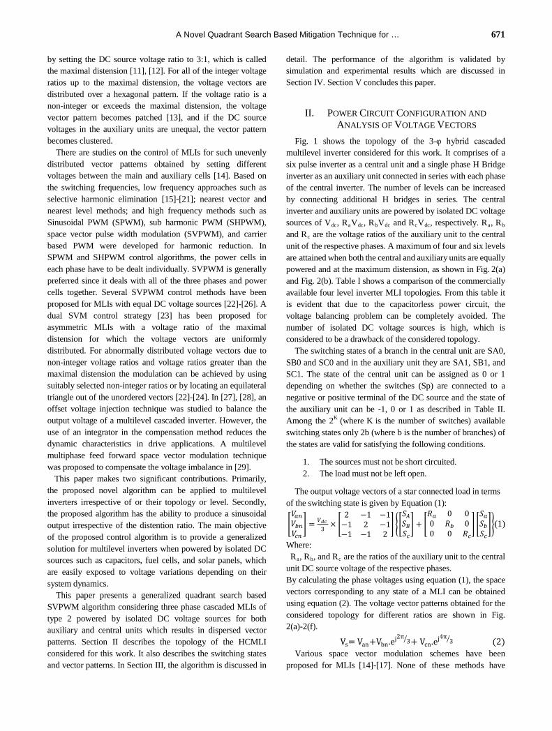
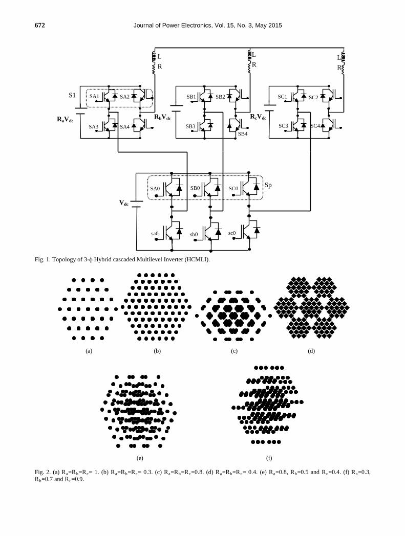
Fig. 1 shows the topology of the 3-φ hybrid cascaded multilevel inverter considered for this work. It comprises of a six pulse inverter as a central unit and a single phase H Bridge inverter as an auxiliary unit connected in series with each phase of the central inverter. The number of levels can be increased by connecting additional H bridges in series. The central inverter and auxiliary units are powered by isolated DC voltage sources of Vdc, RaVdc, RbVdc and RcVdc, respectively. Ra, Rb and Rc are the voltage ratios of the auxiliary unit to the central unit of the respective phases. A maximum of four and six levels are attained when both the central and auxiliary units are equally powered and at the maximum distension, as shown in Fig. 2(a) and Fig. 2(b). Table I shows a comparison of the commercially available four level inverter MLI topologies. From this table it is evident that due to the capacitorless power circuit, the voltage balancing problem can be completely avoided. The number of isolated DC voltage sources is high, which is considered to be a drawback of the considered topology.
The switching states of a branch in the central unit are SA0, SB0 and SC0 and in the auxiliary unit they are SA1, SB1, and SC1. The state of the central unit can be assigned as 0 or 1 depending on whether the switches (Sp) are connected to a negative or positive terminal of the DC source and the state of the auxiliary unit can be -1, 0 or 1 as described in Table II. Among the 2K (where K is the number of switches) available switching states only 2b (where b is the number of branches) of the states are valid for satisfying the following conditions.
1. The sources must not be short circuited. 2. The load must not be left open.
The output voltage vectors of a star connected load in terms of the switching state is given by Equation (1):
�𝑉𝑎𝑛𝑉𝑏𝑛𝑉𝑐𝑛
� = 𝑉𝑑𝑐
3× �
2 −1 −1−1 2 −1−1 −1 2
� ��𝑆𝐴𝑆𝐵𝑆𝑐� + �
𝑅𝑎 0 00 𝑅𝑏 00 0 𝑅𝑐
� �𝑆𝑎𝑆𝑏𝑆𝑐��(1)
Where: Ra, Rb, and Rc are the ratios of the auxiliary unit to the central unit DC source voltage of the respective phases. By calculating the phase voltages using equation (1), the space vectors corresponding to any state of a MLI can be obtained using equation (2). The voltage vector patterns obtained for the considered topology for different ratios are shown in Fig. 2(a)-2(f).
Vs= Van+Vbn.ej2π 3� + Vcn.ej4π 3� (2) Various space vector modulation schemes have been
proposed for MLIs [14]-[17]. None of these methods have
672 Journal of Power Electronics, Vol. 15, No. 3, May 2015
(a) (b) (c) (d)
(e) (f)
Fig. 2. (a) Ra=Rb=Rc= 1. (b) Ra=Rb=Rc= 0.3. (c) Ra=Rb=Rc=0.8. (d) Ra=Rb=Rc= 0.4. (e) Ra=0.8, Rb=0.5 and Rc=0.4. (f) Ra=0.3, Rb=0.7 and Rc=0.9.
SA1 SA2
SA3 SA4
SB1 SB2
SB3 SB4
SC1 SC2
SC3 SC4
SA0 SB0 SC0
sa0 sb0 sc0
Vdc
RaVdc RbVdc RcVdc
L R
L R
L R
Sp
S1
Fig. 1. Topology of 3-ɸ Hybrid cascaded Multilevel Inverter (HCMLI).
A Novel Quadrant Search Based Mitigation Technique for … 673
TABLE I COMPARISON OF THE COMMERCIALLY AVAILABLE FOUR LEVEL MULTILEVEL TOPOLOGIES
TABLE II
SWITCHING STATES OF THE INVERTER UNITS Central Unit Auxiliary Unit
Switch Sp State
Switch S1 State SA1 SA2
ON 1 OFF OFF 0 OFF ON 1
OFF 0 ON OFF -1 ON ON 0
addressed the issue of different voltage sources (Ra ≠ Rb ≠ Rc) in the auxiliary cells. Fig. 2(e) and Fig. 2(f) portray the vector pattern for unequal voltage ratios (Ra ≠ Rb ≠ Rc) in the auxiliary units.
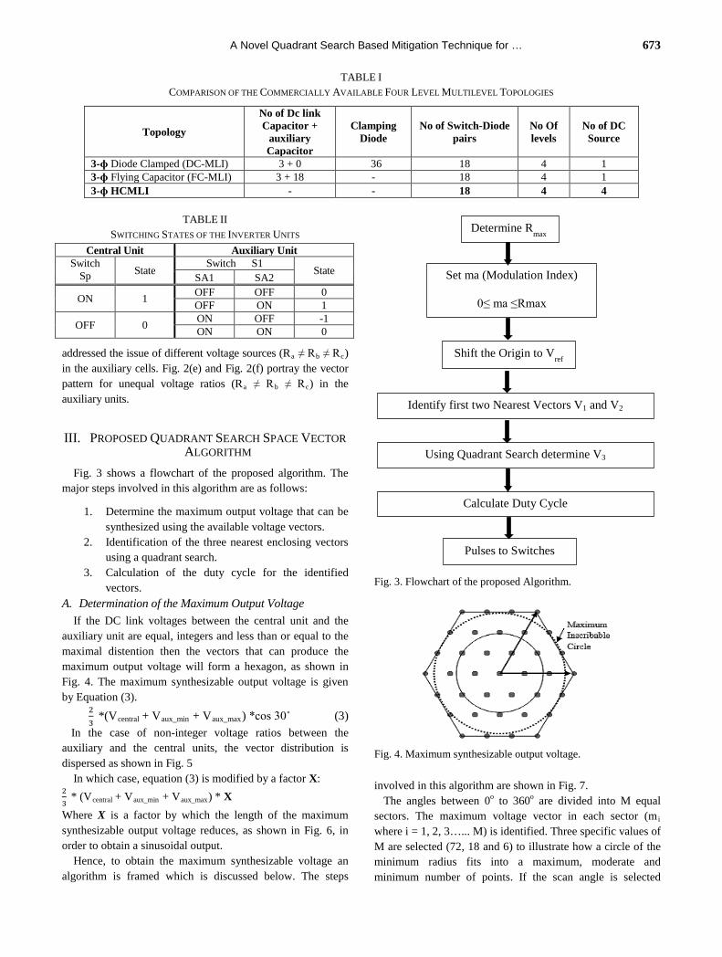
III. PROPOSED QUADRANT SEARCH SPACE VECTOR ALGORITHM
Fig. 3 shows a flowchart of the proposed algorithm. The major steps involved in this algorithm are as follows:
1. Determine the maximum output voltage that can be synthesized using the available voltage vectors.
2. Identification of the three nearest enclosing vectors using a quadrant search.
3. Calculation of the duty cycle for the identified vectors.
A. Determination of the Maximum Output Voltage If the DC link voltages between the central unit and the
auxiliary unit are equal, integers and less than or equal to the maximal distention then the vectors that can produce the maximum output voltage will form a hexagon, as shown in Fig. 4. The maximum synthesizable output voltage is given by Equation (3).
23 *(Vcentral + Vaux_min + Vaux_max) *cos 30˚ (3)
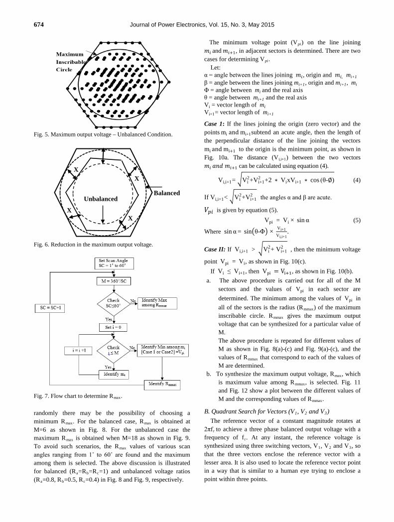
In the case of non-integer voltage ratios between the auxiliary and the central units, the vector distribution is dispersed as shown in Fig. 5
In which case, equation (3) is modified by a factor X: 23 * (Vcentral + Vaux_min + Vaux_max) * X
Where X is a factor by which the length of the maximum synthesizable output voltage reduces, as shown in Fig. 6, in order to obtain a sinusoidal output.
Hence, to obtain the maximum synthesizable voltage an algorithm is framed which is discussed below. The steps
Fig. 3. Flowchart of the proposed Algorithm.
Fig. 4. Maximum synthesizable output voltage.
involved in this algorithm are shown in Fig. 7. The angles between 0o to 360o are divided into M equal
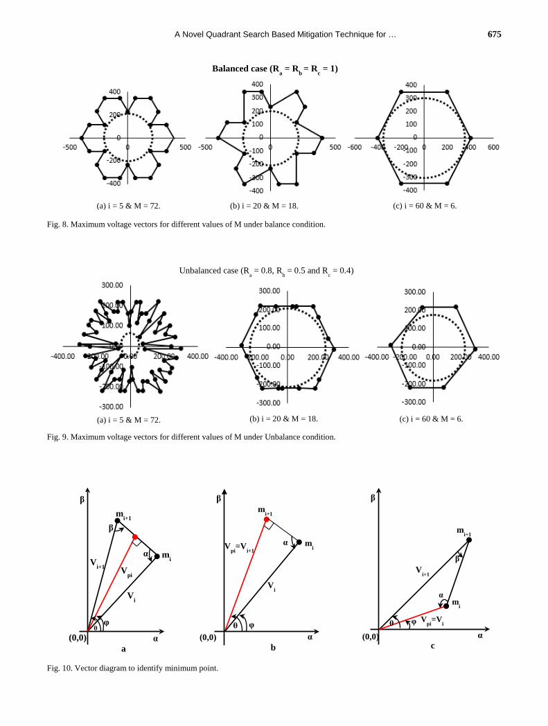
sectors. The maximum voltage vector in each sector (mi where i = 1, 2, 3…... M) is identified. Three specific values of M are selected (72, 18 and 6) to illustrate how a circle of the minimum radius fits into a maximum, moderate and minimum number of points. If the scan angle is selected
Topology
No of Dc link Capacitor +
auxiliary Capacitor
Clamping Diode
No of Switch-Diode pairs
No Of levels
No of DC Source
3-ɸ Diode Clamped (DC-MLI) 3 + 0 36 18 4 1 3-ɸ Flying Capacitor (FC-MLI) 3 + 18 - 18 4 1 3-ɸ HCMLI - - 18 4 4
Determine Rmax
Set ma (Modulation Index)
0≤ ma ≤Rmax
Shift the Origin to Vref
Identify first two Nearest Vectors V1 and V2
Using Quadrant Search determine V3
Calculate Duty Cycle
Pulses to Switches
674 Journal of Power Electronics, Vol. 15, No. 3, May 2015
Fig. 5. Maximum output voltage – Unbalanced Condition.
Fig. 6. Reduction in the maximum output voltage.
Fig. 7. Flow chart to determine Rmax. randomly there may be the possibility of choosing a minimum Rmax. For the balanced case, Rmax is obtained at M=6 as shown in Fig. 8. For the unbalanced case the maximum Rmax is obtained when M=18 as shown in Fig. 9. To avoid such scenarios, the Rmax values of various scan angles ranging from 1˚ to 60˚ are found and the maximum among them is selected. The above discussion is illustrated for balanced (Ra=Rb=Rc=1) and unbalanced voltage ratios (Ra=0.8, Rb=0.5, Rc=0.4) in Fig. 8 and Fig. 9, respectively.
The minimum voltage point (Vpi) on the line joining 𝑚𝑖 and 𝑚𝑖+1, in adjacent sectors is determined. There are two cases for determining Vpi.
Let: α = angle between the lines joining 𝑚𝑖, origin and 𝑚𝑖, mi+1 β = angle between the lines joining mi+1, origin and mi+1, mi Φ = angle between mi and the real axis θ = angle between mi+1 and the real axis Vi = vector length of mi Vi+1= vector length of mi+1
Case 1: If the lines joining the origin (zero vector) and the points mi and mi+1subtend an acute angle, then the length of the perpendicular distance of the line joining the vectors mi and mi+1 to the origin is the minimum point, as shown in Fig. 10a. The distance (Vi,i+1) between the two vectors 𝑚𝑖 𝑎𝑛𝑑 𝑚𝑖+1 can be calculated using equation (4).
Vi,i+1= �Vi2+Vi+1
2 +2 ∗ ViхVi+1 ∗ cos (θ-∅) (4)
If Vi,i+1< �Vi2+Vi+1
2 the angles α and β are acute.
𝑉𝑝𝑖 is given by equation (5). Vpi = Vi × sin α (5)
Where sin α = sin�θ-Φ� × Vi+1Vi,i+1
.
Case II: If Vi,i+1 > �Vi2+ Vi+1
2 , then the minimum voltage
point Vpi = Vi, as shown in Fig. 10(c). If Vi ≤ Vi+1, then Vpi = Vi+1, as shown in Fig. 10(b).
a. The above procedure is carried out for all of the M sectors and the values of Vpi in each sector are determined. The minimum among the values of Vpi in all of the sectors is the radius (Rmmax) of the maximum inscribable circle. Rmmax gives the maximum output voltage that can be synthesized for a particular value of M. The above procedure is repeated for different values of M as shown in Fig. 8(a)-(c) and Fig. 9(a)-(c), and the values of Rmmax that correspond to each of the values of M are determined.
b. To synthesize the maximum output voltage, Rmax, which is maximum value among Rmmax, is selected. Fig. 11 and Fig. 12 show a plot between the different values of M and the corresponding values of Rmmax.
B. Quadrant Search for Vectors (V1, V2 and V3) The reference vector of a constant magnitude rotates at
2πf r to achieve a three phase balanced output voltage with a frequency of fr. At any instant, the reference voltage is synthesized using three switching vectors, V1, V2 and V3, so that the three vectors enclose the reference vector with a lesser area. It is also used to locate the reference vector point in a way that is similar to a human eye trying to enclose a point within three points.
X
X X
X
Balanced Unbalanced
A Novel Quadrant Search Based Mitigation Technique for … 675
Fig. 8. Maximum voltage vectors for different values of M under balance condition.
Fig. 9. Maximum voltage vectors for different values of M under Unbalance condition.
Fig. 10. Vector diagram to identify minimum point.
(a) i = 5 & M = 72. (b) i = 20 & M = 18. (c) i = 60 & M = 6.
Balanced case (Ra = Rb = Rc = 1)
M vs Rmax
Unbalanced case (Ra = 0.8, R
b = 0.5 and R
c = 0.4)
(a) i = 5 & M = 72. (b) i = 20 & M = 18. (c) i = 60 & M = 6.
mi+1
mi
θ φ
Vpi=Vi+1
Vi
α
(0,0) α
β
(0,0)
α
φ θ
Vi
Vpi Vi+1
β mi+1
mi
(0,0)
β
α a b c
θ φ
α
β Vi+1
Vpi=Vi
mi+1
mi
β
α
676 Journal of Power Electronics, Vol. 15, No. 3, May 2015
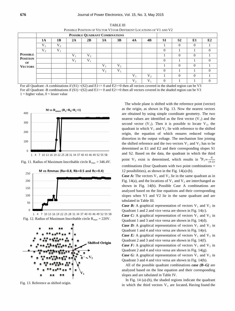
TABLE III POSSIBLE POSITION OF VECTOR V3 FOR DIFFERENT LOCATIONS OF V1 AND V2
POSSIBLE QUADRANT COMBINATIONS
POSSIBLE POSITION
OF VECTORS
1A 1B 2A 2B 3A 3B 4A 4B S1 S2 E1 E2 V1 V2 1 0 0 1 V2 V1 0 1 1 0
V1 V2 1 0 0 1 V2 V1 0 1 1 0 V1 V2 1 0 0 1 V2 V1 0 1 1 0 V1 V2 1 0 0 1 V2 V1 0 1 1 0
For all Quadrant -A combinations if (S1) >(S2) and E1<= 0 and E2>=0 then all vectors covered in the shaded region can be V3 For all Quadrant -B combinations if (S1) <(S2) and E1>= 0 and E2<=0 then all vectors covered in the shaded region can be V3 1 = higher value, 0 = lesser value
Fig. 11. Radius of Maximum Inscribable circle Rmax = 346.4V.
Fig. 12. Radius of Maximum Inscribable circle Rmax = 220V.
Fig. 13. Reference as shifted origin.
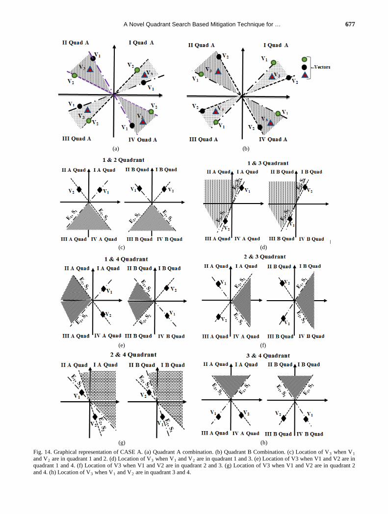
The whole plane is shifted with the reference point (vector) as the origin, as shown in Fig. 13. Now the nearest vectors are obtained by using simple coordinate geometry. The two nearest values are identified as the first vector (V1) and the second vector (V2). Then it is possible to locate V3, the quadrant in which V1 and V2 lie with reference to the shifted origin, the equation of which ensures reduced voltage distortion in the output voltage. The mechanism line joining the shifted reference and the two vectors V1 and V2 has to be determined as E1 and E2 and their corresponding slopes S1 and S2. Based on the data, the quadrant in which the third point V3 exist is determined, which results in 4P2= 4!
(4-2)!
combinations (four Quadrants with two point combinations = 12 possibilities), as shown in the Fig. 14(a)-(h). Case A: The vectors V1 and V2 lie in the same quadrant as in Fig. 14(a), and the locations of V1 and V2 are interchanged as shown in Fig. 14(b). Possible Case A combinations are analyzed based on the line equations and their corresponding slopes when V1 and V2 lie in the same quadrant and are tabulated in Table III. Case B: A graphical representation of vectors V1 and V2 in Quadrant 1 and 2 and vice versa are shown in Fig. 14(c). Case C: A graphical representation of vectors V1 and V2 in Quadrant 1 and 3 and vice versa are shown in Fig. 14(d). Case D: A graphical representation of vectors V1 and V2 in Quadrant 1 and 4 and vice versa are shown in Fig. 14(e). Case E: A graphical representation of vectors V1 and V2 in Quadrant 2 and 3 and vice versa are shown in Fig. 14(f). Case F: A graphical representation of vectors V1 and V2 in Quadrant 2 and 4 and vice versa are shown in Fig. 14(g). Case G: A graphical representation of vectors V1 and V2 in Quadrant 3 and 4 and vice versa are shown in Fig. 14(h).
All of the possible quadrant combinations case (B–G) are analyzed based on the line equation and their corresponding slopes and are tabulated in Table IV.
In Fig. 14 (a)-(h), the shaded regions indicate the quadrant in which the third vectors V3 are located. Having found the
0
100
200
300
400
1 4 7 10 13 16 19 22 25 28 31 34 37 40 43 46 49 52 55 58
M vs Rmmax (Ra=Rb=Rc=1)
0
50
100
150
200
250
1 4 7 10 13 16 19 22 25 28 31 34 37 40 43 46 49 52 55 58
M vs Rmmax (Ra=0.8, Rb=0.5 and Rc=0.4)
A Novel Quadrant Search Based Mitigation Technique for … 677
(a) (b)
(c) (d)
(e) (f)
(g) (h)
Fig. 14. Graphical representation of CASE A. (a) Quadrant A combination. (b) Quadrant B Combination. (c) Location of V3 when V1 and V2 are in quadrant 1 and 2. (d) Location of V3 when V1 and V2 are in quadrant 1 and 3. (e) Location of V3 when V1 and V2 are in quadrant 1 and 4. (f) Location of V3 when V1 and V2 are in quadrant 2 and 3. (g) Location of V3 when V1 and V2 are in quadrant 2 and 4. (h) Location of V3 when V1 and V2 are in quadrant 3 and 4.
678 Journal of Power Electronics, Vol. 15, No. 3, May 2015
TABLE IV POSSIBLE POSITION OF VECTOR V3 FOR DIFFERENT LOCATIONS OF V1 AND V2
POSSIBLE QUADRANT COMBINATIONS
POSSIBLE LOCATION
OF VECTORS
1A 1B 2A 2B 3A 3B 4A 4B S1 S2 E1 E2 V1 V2 1 0 1 0
V2 V1 0 1 0 1 V1 V2 1 0 1 0
V2 V1 0 1 0 1 V1 V2 1 0 0 1
V2 V1 0 1 1 0 V1 V2 1 0 0 1 V2 V1 0 1 1 0 V1 V2 1 0 1 0 V2 V1 0 1 0 1 V1 V2 1 0 1 0 V2 V1 0 1 0 1
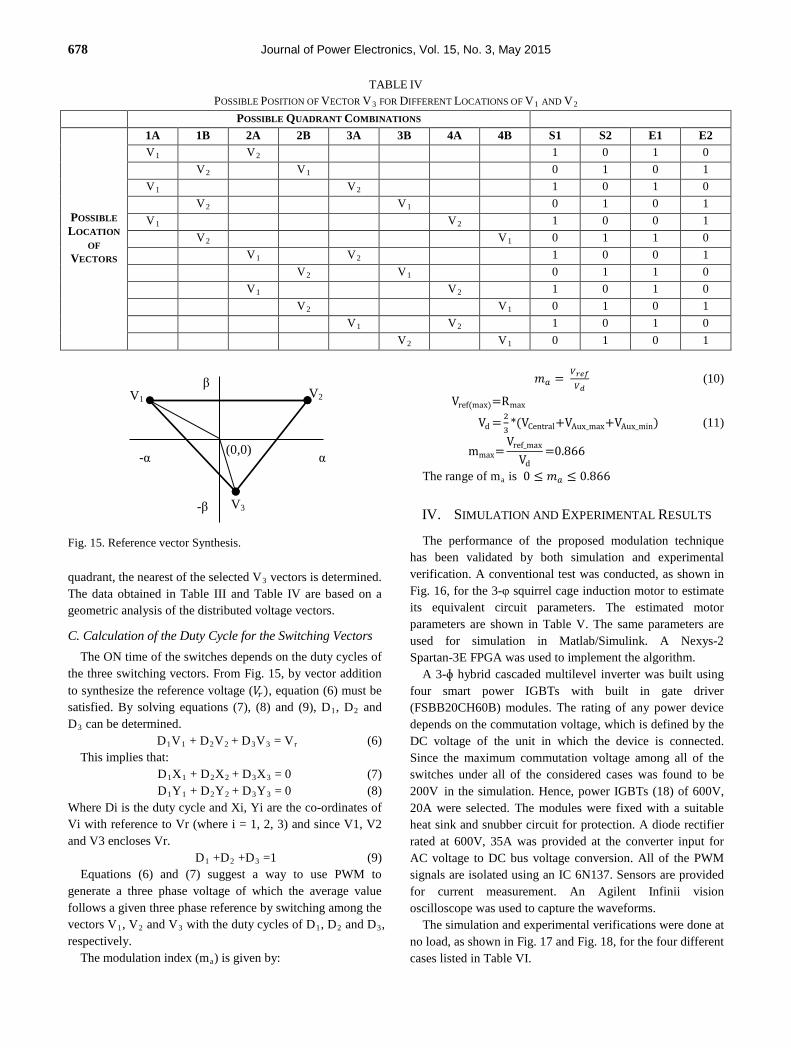
Fig. 15. Reference vector Synthesis. quadrant, the nearest of the selected V3 vectors is determined. The data obtained in Table III and Table IV are based on a geometric analysis of the distributed voltage vectors.
C. Calculation of the Duty Cycle for the Switching Vectors
The ON time of the switches depends on the duty cycles of the three switching vectors. From Fig. 15, by vector addition to synthesize the reference voltage (𝑉𝑟), equation (6) must be satisfied. By solving equations (7), (8) and (9), D1, D2 and D3 can be determined.
D1V1 + D2V2 + D3V3 = Vr (6) This implies that:
D1X1 + D2X2 + D3X3 = 0 (7) D1Y1 + D2Y2 + D3Y3 = 0 (8)
Where Di is the duty cycle and Xi, Yi are the co-ordinates of Vi with reference to Vr (where i = 1, 2, 3) and since V1, V2 and V3 encloses Vr.
D1 +D2 +D3 =1 (9) Equations (6) and (7) suggest a way to use PWM to
generate a three phase voltage of which the average value follows a given three phase reference by switching among the vectors V1, V2 and V3 with the duty cycles of D1, D2 and D3, respectively.
The modulation index (ma) is given by:
𝑚𝑎 = 𝑉𝑟𝑒𝑓𝑉𝑑
(10)
Vref(max)=Rmax
Vd =23
*(VCentral+VAux_max+VAux_min) (11)
mmax=Vref_max
Vd=0.866
The range of ma is 0 ≤ 𝑚𝑎 ≤ 0.866
IV. SIMULATION AND EXPERIMENTAL RESULTS
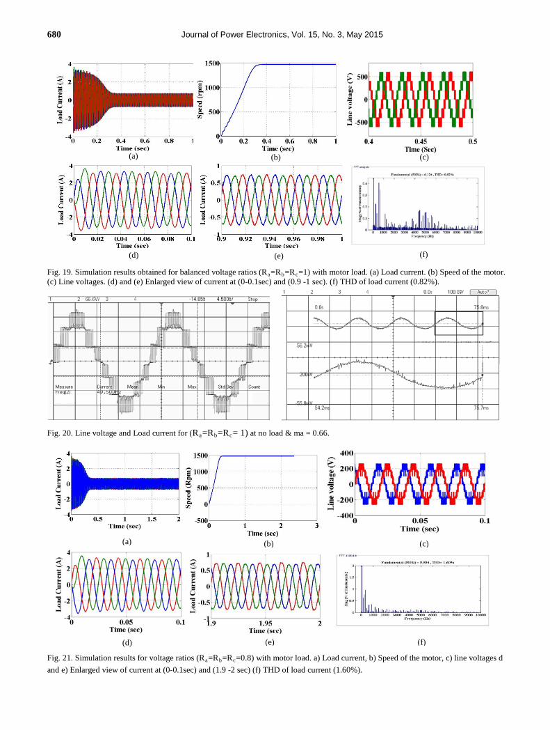
The performance of the proposed modulation technique has been validated by both simulation and experimental verification. A conventional test was conducted, as shown in Fig. 16, for the 3-φ squirrel cage induction motor to estimate its equivalent circuit parameters. The estimated motor parameters are shown in Table V. The same parameters are used for simulation in Matlab/Simulink. A Nexys-2 Spartan-3E FPGA was used to implement the algorithm.
A 3-ɸ hybrid cascaded multilevel inverter was built using four smart power IGBTs with built in gate driver (FSBB20CH60B) modules. The rating of any power device depends on the commutation voltage, which is defined by the DC voltage of the unit in which the device is connected. Since the maximum commutation voltage among all of the switches under all of the considered cases was found to be 200V in the simulation. Hence, power IGBTs (18) of 600V, 20A were selected. The modules were fixed with a suitable heat sink and snubber circuit for protection. A diode rectifier rated at 600V, 35A was provided at the converter input for AC voltage to DC bus voltage conversion. All of the PWM signals are isolated using an IC 6N137. Sensors are provided for current measurement. An Agilent Infinii vision oscilloscope was used to capture the waveforms.
The simulation and experimental verifications were done at no load, as shown in Fig. 17 and Fig. 18, for the four different cases listed in Table VI.
(0,0)
V3
α
β
-α
-β
V1 V2
A Novel Quadrant Search Based Mitigation Technique for … 679
TABLE V MOTOR SPECIFICATIONS
Rated Power 0.37kw (0.5Hp) Rated Voltage 415 (rms) Rated Current 1.2A (star) No of Pole Pairs 2 Rated torque 2.54 Nm Rated speed 1500 rpm Frequency 50Hz Duty S1 Stator Resistance (Rs) 32.71Ω Stator Inductance (LIs) 0.1035H Rotor Resistance (Rr’) 20.47 Ω Rotor Inductance (LIr’) 0.1028H Mutual Inductance (Lm) 1.1H
TABLE VI SIMULATION PARAMETERS
Value
3φ Induction Motor (Star) Refer Table. 5 Central Cell DC Voltage 200 V
Output Voltage frequency 50 Hz
Switching frequency 5 kHz
Auxiliary cell DC Voltage Source Case I – Balanced Condition Ra=Rb=Rc =1
Case II-Above Maximum distention
Ra=Rb=Rc=0.8
Case III - Unequal Voltage ratio Ra=0.8, Rb=0.5 and Rc=0.4
Case IV- Unequal Voltage ratio Ra = 0.3, Rb = 0.7and Rc=0.9
Fig. 16. Conventional test to estimate the motor parameters. Case I-Balanced Condition (Ra = Rb = Rc = 1) Simulation and experimental verifications were carried out by setting Vdc=200V, RaVdc=RbVdc=RcVdc =200V and operating the machine at no load. Rmax for this case was found to be 346.6V. At a modulation index of ma = 0.66, VL (peak) = 578V,
Fig. 17. Simulation of the Algorithm by MATLAB/Simulink.
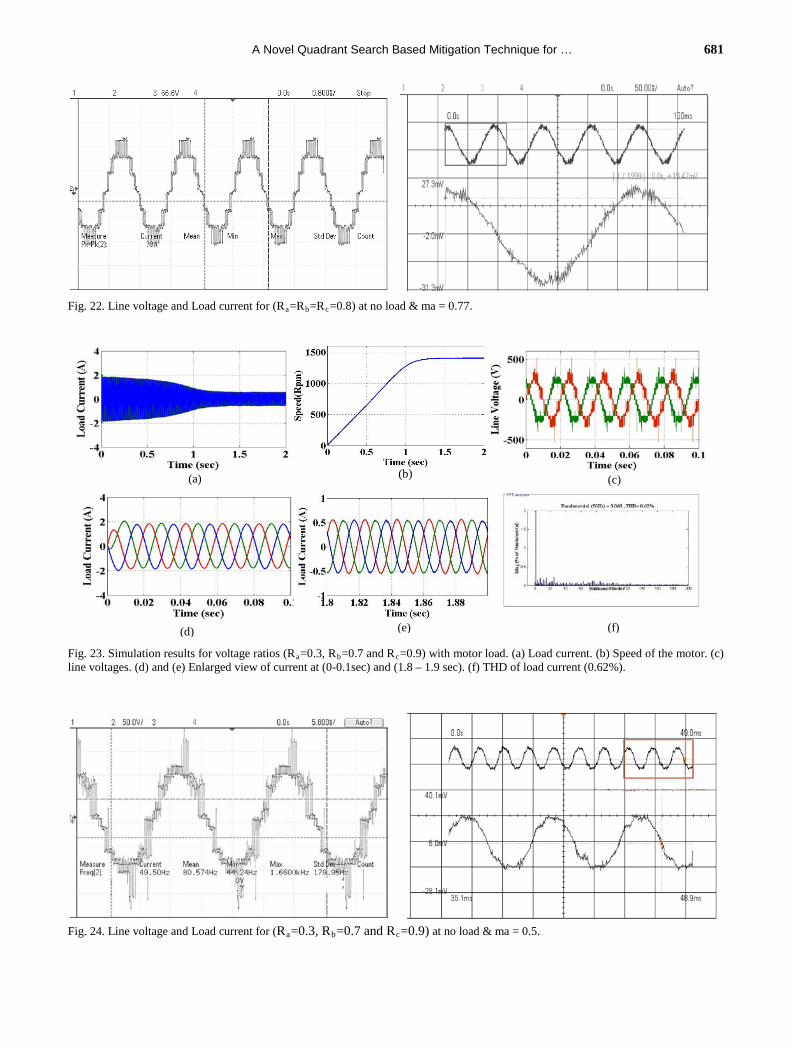
Fig. 18. Experimental setup for verification of the Algorithm. VL (rms) = 408V. In addition, IL (peak) = 0.714A, IL (rms) = 0.505A and speed of the motor was 1473 rpm. As shown in Fig. 19 and Fig. 20 similar results were obtained in both the simulation and the experiment. The THD of the load current was found to be 0.82%.
Case II-Above the Maximum distention (Ra = Rb = Rc = 0.8) Voltages of VDC = 200V, RAVDC=RbVDC=RCVDC=160V were applied for both the simulation and experimental setups and the machine was operated at no load. The Rmax for this case was found to be 300.5V. At a modulation index of ma = 0.77, VL (peak) = 266.9V, VL (rms) = 188.7V. In addition, IL (peak) = 0.72A, IL (rms) = 0.51A and speed of the motor was 1473 rpm. From Fig. 21 and Fig. 22 it is evident that similar results were obtained from both the simulation and the experiment. The THD of the load current was 1.60%.
Case III- Unbalance ratios Ra = 0.3, Rb = 0.7 and Rc = 0.9
680 Journal of Power Electronics, Vol. 15, No. 3, May 2015
Fig. 19. Simulation results obtained for balanced voltage ratios (Ra=Rb=Rc=1) with motor load. (a) Load current. (b) Speed of the motor. (c) Line voltages. (d) and (e) Enlarged view of current at (0-0.1sec) and (0.9 -1 sec). (f) THD of load current (0.82%).
Fig. 20. Line voltage and Load current for (Ra=Rb=Rc= 1) at no load & ma = 0.66.
Fig. 21. Simulation results for voltage ratios (Ra=Rb=Rc=0.8) with motor load. a) Load current, b) Speed of the motor, c) line voltages d and e) Enlarged view of current at (0-0.1sec) and (1.9 -2 sec) (f) THD of load current (1.60%).
(a) (b) (c)
(d) (e) (f)
(e)
(a) (b) (c)
(d) (f)
A Novel Quadrant Search Based Mitigation Technique for … 681
Fig. 22. Line voltage and Load current for (Ra=Rb=Rc=0.8) at no load & ma = 0.77.
Fig. 23. Simulation results for voltage ratios (Ra=0.3, Rb=0.7 and Rc=0.9) with motor load. (a) Load current. (b) Speed of the motor. (c) line voltages. (d) and (e) Enlarged view of current at (0-0.1sec) and (1.8 – 1.9 sec). (f) THD of load current (0.62%).
Fig. 24. Line voltage and Load current for (Ra=0.3, Rb=0.7 and Rc=0.9) at no load & ma = 0.5.
(e) (d)
(a) (b) (c)
(f)
682 Journal of Power Electronics, Vol. 15, No. 3, May 2015
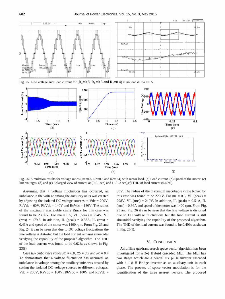
Fig. 25. Line voltage and Load current for (Ra=0.8, Rb=0.5 and Rc=0.4) at no load & ma = 0.5.
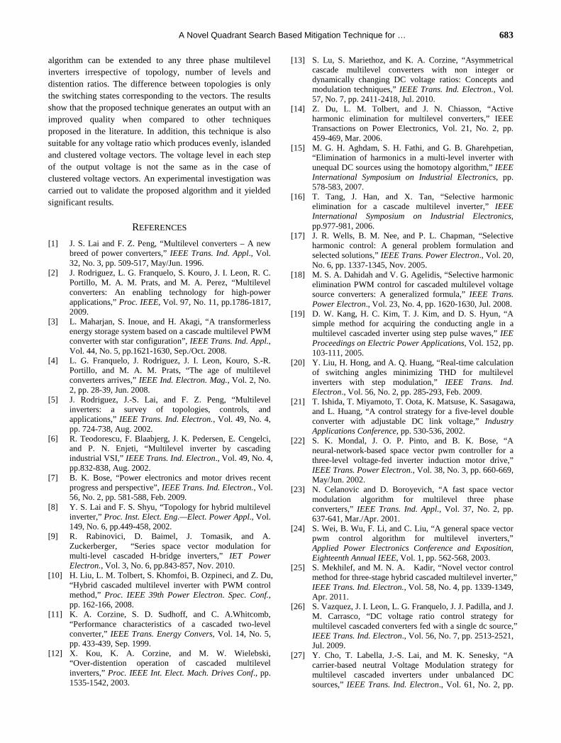
Fig. 26. Simulation results for voltage ratios (Ra=0.8, Rb=0.5 and Rc=0.4) with motor load. (a) Load current. (b) Speed of the motor. (c) line voltages. (d) and (e) Enlarged view of current at (0-0.1sec) and (1.9 -2 sec),(f) THD of load current (0.49%).
Assuming that a voltage fluctuation has occurred, an unbalance in the voltage among the auxiliary units was created by adjusting the isolated DC voltage sources to Vdc = 200V, RaVdc = 60V, RbVdc = 140V and RcVdc = 180V. The radius of the maximum inscribable circle Rmax for this case was found to be 230.6V. For ma = 0.5, VL (peak) = 254V, VL (rms) = 179.6. In addition, IL (peak) = 0.58A, IL (rms) = 0.41A and speed of the motor was 1400 rpm. From Fig. 23 and Fig. 24 it can be seen that due to DC voltage fluctuations the line voltage is distorted but the load current remains sinusoidal verifying the capability of the proposed algorithm. The THD of the load current was found to be 0.62% as shown in Fig. 23(f).
Case III- Unbalance ratios Ra = 0.8, Rb = 0.5 and Rc = 0.4 To demonstrate that a voltage fluctuation has occurred, an unbalance in voltage among the auxiliary units was created by setting the isolated DC voltage sources to different voltages, Vdc = 200V, RaVdc = 160V, RbVdc = 100V and RcVdc =
80V. The radius of the maximum inscribable circle Rmax for this case was found to be 220.V. For ma = 0.5, VL (peak) = 298V, VL (rms) = 210V. In addition, IL (peak) = 0.51A, IL (rms) = 0.36A and speed of the motor was 1400 rpm. From Fig. 25 and Fig. 26 it can be seen that the line voltage is distorted due to DC voltage fluctuations but the load current is still sinusoidal verifying the capability of the proposed algorithm. The THD of the load current was found to be 0.49% as shown in Fig. 26(f).
V. CONCLUSION An offline quadrant search space vector algorithm has been
investigated for a 3-ɸ Hybrid cascaded MLI. The MLI has two stages which are a central six pulse inverter cascaded with a 1-ɸ H Bridge inverter as an auxiliary unit in each phase. The process of space vector modulation is for the identification of the three nearest vectors. The proposed
(a) (b) (c)
(e) (d) (f)
A Novel Quadrant Search Based Mitigation Technique for … 683
algorithm can be extended to any three phase multilevel inverters irrespective of topology, number of levels and distention ratios. The difference between topologies is only the switching states corresponding to the vectors. The results show that the proposed technique generates an output with an improved quality when compared to other techniques proposed in the literature. In addition, this technique is also suitable for any voltage ratio which produces evenly, islanded and clustered voltage vectors. The voltage level in each step of the output voltage is not the same as in the case of clustered voltage vectors. An experimental investigation was carried out to validate the proposed algorithm and it yielded significant results.
REFERENCES [1] J. S. Lai and F. Z. Peng, “Multilevel converters – A new
breed of power converters,” IEEE Trans. Ind. Appl., Vol. 32, No. 3, pp. 509-517, May/Jun. 1996.
[2] J. Rodriguez, L. G. Franquelo, S. Kouro, J. I. Leon, R. C. Portillo, M. A. M. Prats, and M. A. Perez, “Multilevel converters: An enabling technology for high-power applications,” Proc. IEEE, Vol. 97, No. 11, pp.1786-1817, 2009.
[3] L. Maharjan, S. Inoue, and H. Akagi, “A transformerless energy storage system based on a cascade multilevel PWM converter with star configuration”, IEEE Trans. Ind. Appl., Vol. 44, No. 5, pp.1621-1630, Sep./Oct. 2008.
[4] L. G. Franquelo, J. Rodriguez, J. I. Leon, Kouro, S.-R. Portillo, and M. A. M. Prats, “The age of multilevel converters arrives,” IEEE Ind. Electron. Mag., Vol. 2, No. 2, pp. 28-39, Jun. 2008.
[5] J. Rodriguez, J.-S. Lai, and F. Z. Peng, “Multilevel inverters: a survey of topologies, controls, and applications,” IEEE Trans. Ind. Electron., Vol. 49, No. 4, pp. 724-738, Aug. 2002.
[6] R. Teodorescu, F. Blaabjerg, J. K. Pedersen, E. Cengelci, and P. N. Enjeti, “Multilevel inverter by cascading industrial VSI,” IEEE Trans. Ind. Electron., Vol. 49, No. 4, pp.832-838, Aug. 2002.
[7] B. K. Bose, “Power electronics and motor drives recent progress and perspective”, IEEE Trans. Ind. Electron., Vol. 56, No. 2, pp. 581-588, Feb. 2009.
[8] Y. S. Lai and F. S. Shyu, “Topology for hybrid multilevel inverter,” Proc. Inst. Elect. Eng.—Elect. Power Appl., Vol. 149, No. 6, pp.449-458, 2002.
[9] R. Rabinovici, D. Baimel, J. Tomasik, and A. Zuckerberger, “Series space vector modulation for multi-level cascaded H-bridge inverters,” IET Power Electron., Vol. 3, No. 6, pp.843-857, Nov. 2010.
[10] H. Liu, L. M. Tolbert, S. Khomfoi, B. Ozpineci, and Z. Du, “Hybrid cascaded multilevel inverter with PWM control method,” Proc. IEEE 39th Power Electron. Spec. Conf., pp. 162-166, 2008.
[11] K. A. Corzine, S. D. Sudhoff, and C. A.Whitcomb, “Performance characteristics of a cascaded two-level converter,” IEEE Trans. Energy Convers, Vol. 14, No. 5, pp. 433-439, Sep. 1999.
[12] X. Kou, K. A. Corzine, and M. W. Wielebski, “Over-distention operation of cascaded multilevel inverters,” Proc. IEEE Int. Elect. Mach. Drives Conf., pp. 1535-1542, 2003.
[13] S. Lu, S. Mariethoz, and K. A. Corzine, “Asymmetrical cascade multilevel converters with non integer or dynamically changing DC voltage ratios: Concepts and modulation techniques,” IEEE Trans. Ind. Electron., Vol. 57, No. 7, pp. 2411-2418, Jul. 2010.
[14] Z. Du, L. M. Tolbert, and J. N. Chiasson, “Active harmonic elimination for multilevel converters,” IEEE Transactions on Power Electronics, Vol. 21, No. 2, pp. 459-469, Mar. 2006.
[15] M. G. H. Aghdam, S. H. Fathi, and G. B. Gharehpetian, “Elimination of harmonics in a multi-level inverter with unequal DC sources using the homotopy algorithm,” IEEE International Symposium on Industrial Electronics, pp. 578-583, 2007.
[16] T. Tang, J. Han, and X. Tan, “Selective harmonic elimination for a cascade multilevel inverter,” IEEE International Symposium on Industrial Electronics, pp.977-981, 2006.
[17] J. R. Wells, B. M. Nee, and P. L. Chapman, “Selective harmonic control: A general problem formulation and selected solutions,” IEEE Trans. Power Electron., Vol. 20, No. 6, pp. 1337-1345, Nov. 2005.
[18] M. S. A. Dahidah and V. G. Agelidis, “Selective harmonic elimination PWM control for cascaded multilevel voltage source converters: A generalized formula,” IEEE Trans. Power Electron., Vol. 23, No. 4, pp. 1620-1630, Jul. 2008.
[19] D. W. Kang, H. C. Kim, T. J. Kim, and D. S. Hyun, “A simple method for acquiring the conducting angle in a multilevel cascaded inverter using step pulse waves,” IEE Proceedings on Electric Power Applications, Vol. 152, pp. 103-111, 2005.
[20] Y. Liu, H. Hong, and A. Q. Huang, “Real-time calculation of switching angles minimizing THD for multilevel inverters with step modulation,” IEEE Trans. Ind. Electron., Vol. 56, No. 2, pp. 285-293, Feb. 2009.
[21] T. Ishida, T. Miyamoto, T. Oota, K. Matsuse, K. Sasagawa, and L. Huang, “A control strategy for a five-level double converter with adjustable DC link voltage,” Industry Applications Conference, pp. 530-536, 2002.
[22] S. K. Mondal, J. O. P. Pinto, and B. K. Bose, “A neural-network-based space vector pwm controller for a three-level voltage-fed inverter induction motor drive,” IEEE Trans. Power Electron., Vol. 38, No. 3, pp. 660-669, May/Jun. 2002.
[23] N. Celanovic and D. Boroyevich, “A fast space vector modulation algorithm for multilevel three phase converters,” IEEE Trans. Ind. Appl., Vol. 37, No. 2, pp. 637-641, Mar./Apr. 2001.
[24] S. Wei, B. Wu, F. Li, and C. Liu, “A general space vector pwm control algorithm for multilevel inverters,” Applied Power Electronics Conference and Exposition, Eighteenth Annual IEEE, Vol. 1, pp. 562-568, 2003.
[25] S. Mekhilef, and M. N. A. Kadir, “Novel vector control method for three-stage hybrid cascaded multilevel inverter,” IEEE Trans. Ind. Electron., Vol. 58, No. 4, pp. 1339-1349, Apr. 2011.
[26] S. Vazquez, J. I. Leon, L. G. Franquelo, J. J. Padilla, and J. M. Carrasco, “DC voltage ratio control strategy for multilevel cascaded converters fed with a single dc source,” IEEE Trans. Ind. Electron., Vol. 56, No. 7, pp. 2513-2521, Jul. 2009.
[27] Y. Cho, T. Labella, J.-S. Lai, and M. K. Senesky, “A carrier-based neutral Voltage Modulation strategy for multilevel cascaded inverters under unbalanced DC sources,” IEEE Trans. Ind. Electron., Vol. 61, No. 2, pp.
684 Journal of Power Electronics, Vol. 15, No. 3, May 2015
625-636, Feb. 2014. [28] Y. M. Park, H. S. Ryu, H. W. Lee, M. G. Jung, and S. H.
Lee, “ Design of a cascaded h-bridge multilevel inverter based on power electronics building blocks and control for high performance,” Journal of Power Electronics, Vol. 10, No. 3, pp. 262-269, May 2010.
[29] F. Carnielutti, H. Pinheiro, and C. Rech, “Generalized Carrier-based modulation strategy for cascaded multilevel converters operating under fault conditions,” IEEE Trans. Ind. Electron., Vol. 59, No. 2, pp. 679-689, Feb. 2012.
Johnson Anitha Roseline received her Bachelor degree in 2002 from the University of Madras, Chennai, India, in 2002. She received and Master degree in 2006 from Anna University. She is presently working as an Assistant Professor in the Department of Electrical and Electronics Engineering at the SSN College of Engineering, Chennai, India.
She has 12 years of academic experience. Her current research interests include power electronics and control.
Subramanian Vijayenthiran received his Bachelor degrees in Electrical and Electronics Engineering from Anna University, Chennai, India, in 2013. He is presently working as Research Assistant in the Department of Electrical and Electronics Engineering at the SSN College of Engineering, Chennai, India. His current
research interest include robotics and power electronics.
Rajini V received her B.E. and M.E. degrees from Annamalai University, Chidambaram, India, and her Ph.D. degree from Anna University, Chennai, India. She is presently a Professor at the SSN College of Engineering, Chennai, India. She has 22 years of academic experience. Her current research interests include power electronics and high voltage
engineering.
Senthil Kumaran Mahadevan received his Bachelor and Master degrees in Electrical and Electronics Engineering from the University of Madras, Chennai, India, in 1999 and 2001, respectively, and his Ph.D. degree from Anna University, Chennai, India, in 2013. He is presently working as an Assistant Professor in the Department of
Electrical and Electronics Engineering at the SSN College of Engineering, Chennai, India. His current research interests include electric drives, control and signal processing,