Embed Size (px)
Citation preview

Hardik Patel-3146504
Embedded System DesignSVE, NIT Kurukshetra
SPINTRONICS….. a new era in electronics

OUTLINE :
• Need ??
• Magnetics and Storage
• Evolution
• GMR
• Hard Disk Drive
• MTJ
• MRAM
• Race Track Memory
• Logical Comparison
• Conclusion
• NEED OF SPINTRONICS ???
Failures of MOORE’s Law….
Law states that “ Transistor counts doubles Every 18 to 24 months”
so because of high packing density increasing we are facing to many problems.
some of the major problems are….
1) SCORCHING HEAT generation making the circuit inoperable
2) QUANTOM EFFECT comes in to play at nanoscale dimension
So, the size of the transistor and other component can’t be reduced further.
As a result other quantum mechanics property of electron ‘SPIN’ is taken in
to consideration. i.e nothing but….
“SPIN + ELECTRONICS = SPINTRONICS”
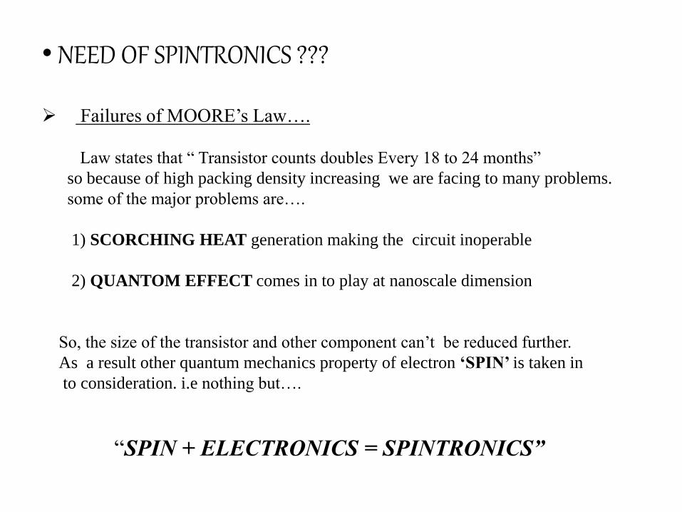
•MAGNETIcs & Storage

• EVOLUTION
CURRENT IN A METALIC CONDUCTOR
In a non magnetic conductor , electron scatters the same amount regardless of spin as a current flow.
How much they scatters determines the resistance of device.
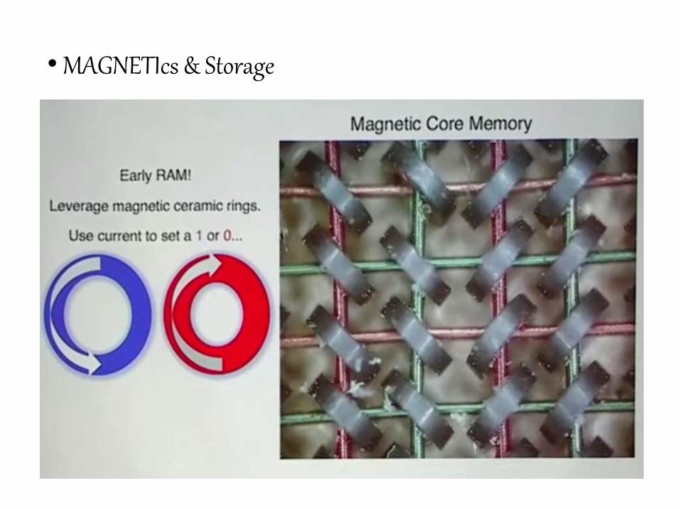
CURRENT IN A FERROMAGNETIC CONDUCTOR
In a ferromagnetic conductor , however , electrons scatters differently depending onwhether they are spin up or spin down.
In this Case , spin up electrons are scatters strongly while the spin down electrons arescattered only weakly.
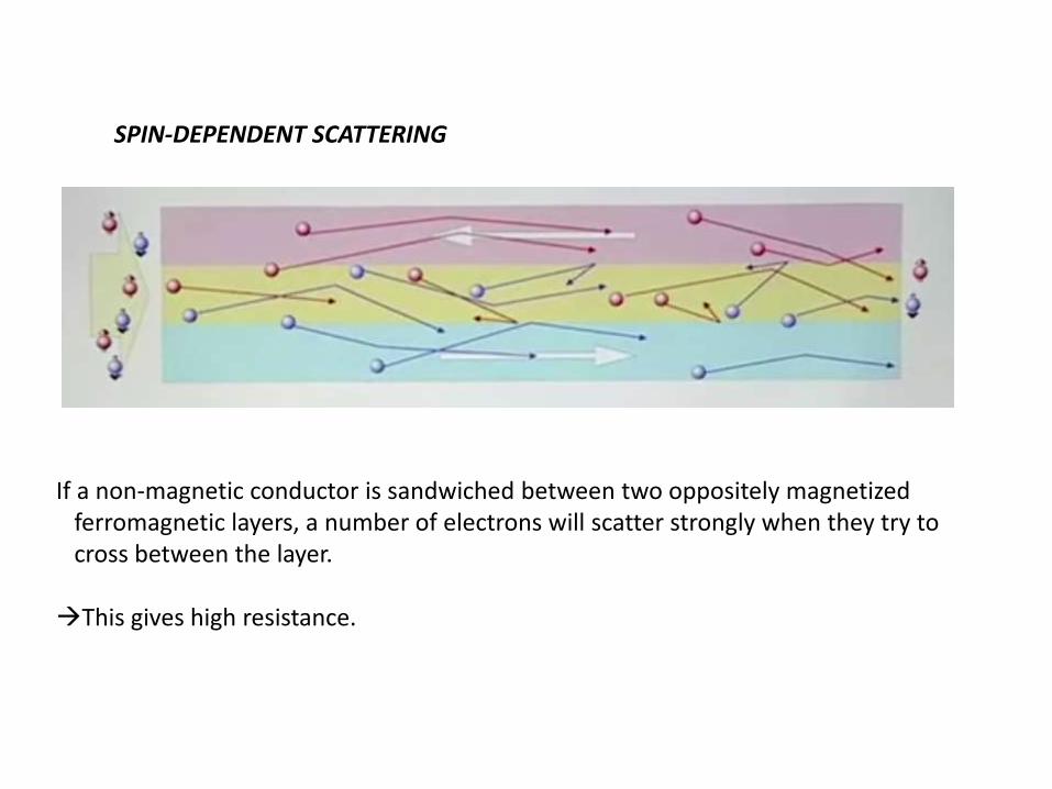
SPIN-DEPENDENT SCATTERING
If a non-magnetic conductor is sandwiched between two oppositely magnetized ferromagnetic layers, a number of electrons will scatter strongly when they try to cross between the layer.
This gives high resistance.
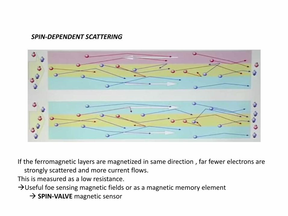
SPIN-DEPENDENT SCATTERING
If the ferromagnetic layers are magnetized in same direction , far fewer electrons are strongly scattered and more current flows.
This is measured as a low resistance.Useful foe sensing magnetic fields or as a magnetic memory element
SPIN-VALVE magnetic sensor
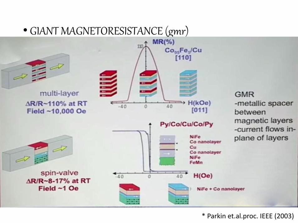
• GIANT MAGNETORESISTANCE (gmr)
* Parkin et.al.proc. IEEE (2003)
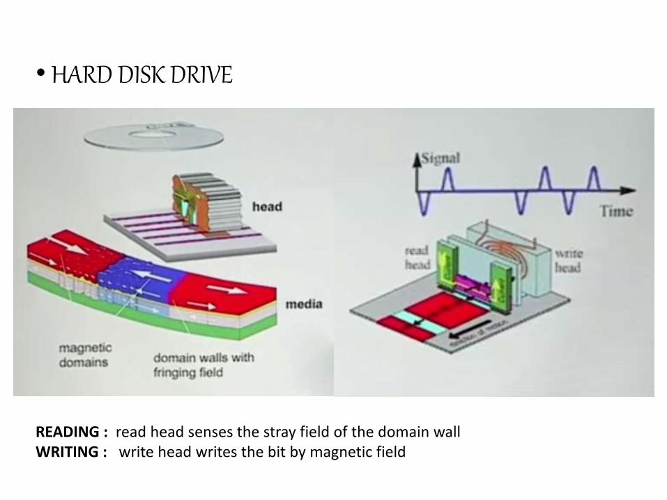
• HARD DISK DRIVE
READING : read head senses the stray field of the domain wallWRITING : write head writes the bit by magnetic field
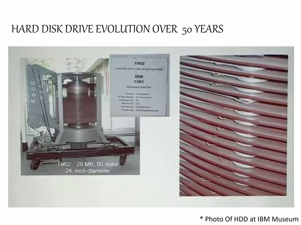
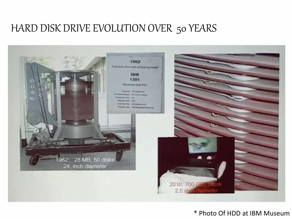
HARD DISK DRIVE EVOLUTION OVER 50 YEARS
* Photo Of HDD at IBM Museum
HARD DISK DRIVE EVOLUTION OVER 50 YEARS
* Photo Of HDD at IBM Museum
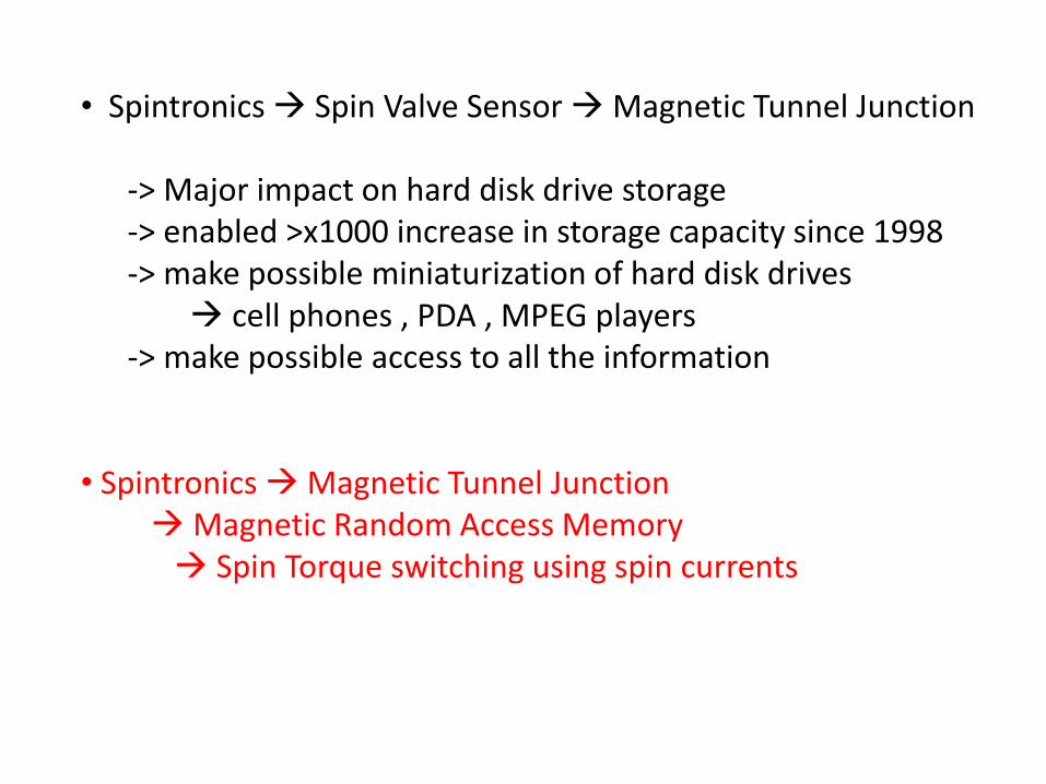
• Spintronics Spin Valve Sensor Magnetic Tunnel Junction
-> Major impact on hard disk drive storage-> enabled >x1000 increase in storage capacity since 1998 -> make possible miniaturization of hard disk drives
cell phones , PDA , MPEG players-> make possible access to all the information
• SpintronicsMagnetic Tunnel JunctionMagnetic Random Access Memory Spin Torque switching using spin currents
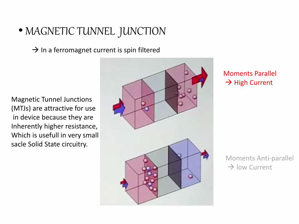
•MAGNETIC TUNNEL JUNCTION
In a ferromagnet current is spin filtered
Magnetic Tunnel Junctions(MTJs) are attractive for usein device because they are
Inherently higher resistance,Which is usefull in very smallsacle Solid State circuitry.
Moments Parallel High Current
Moments Anti-parallel low Current
USEFULL MAGNETIC TUNNEL JUNCTIONS (MTJ) !
- Magnetron or ion beam Sputtered at ambienttemp. on amorphous SiO2
- Artificial antiferromagnetic reference layerneeded!

•MTj electron micrograph
By sandwiching amorphous structure between ferromagnetic layer we canget this type of observation through electron microscope.
*Parkin ,US Patent filed (2003)*Published Nature Materials (2004)
•MTj electron micrograph
By sandwiching amorphous structure between ferromagnetic layer we canget this type of observation through electron microscope.
*Parkin ,US Patent filed (2003)*Published Nature Materials (2004)
•MAGNETORESISTIVE MATERIAL EVOLUTION
Huge room temp. TMR values in MTJs useful for memories and sensing application.[Parkin et al. nature mater.(2004)] ~220% in 2001-2002:400-800% today
*MgO tunnel barriers and method of formation , S.S.P. Parkin, filed August 22,2003
• IBM LABORATORY MANUFACTURING
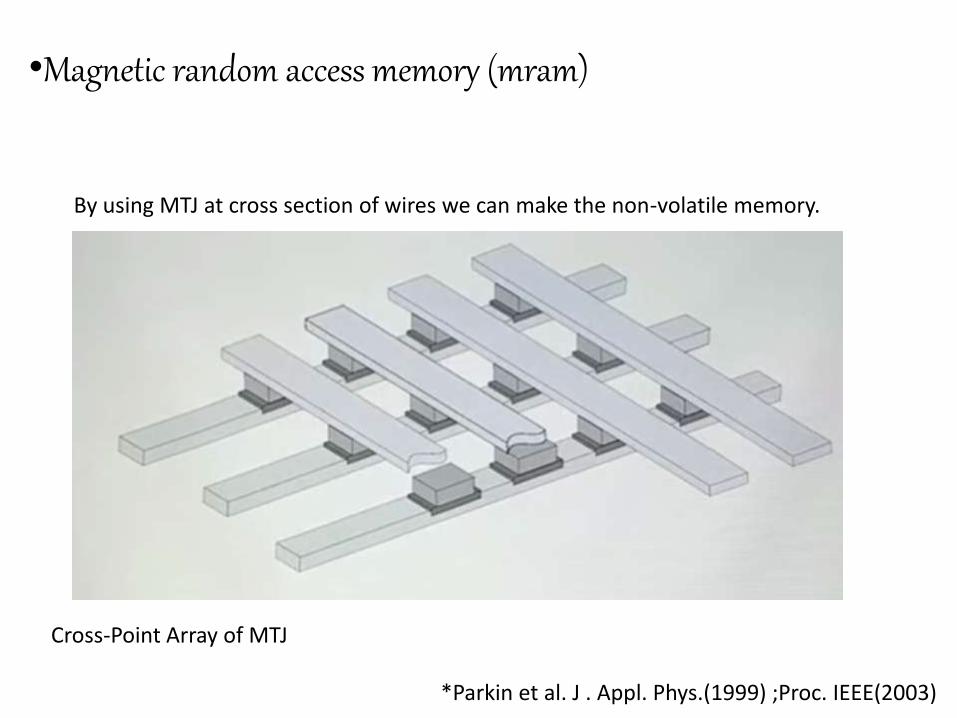
•Magnetic random access memory (mram)
By using MTJ at cross section of wires we can make the non-volatile memory.
Cross-Point Array of MTJ
*Parkin et al. J . Appl. Phys.(1999) ;Proc. IEEE(2003)

Cross-Point Array of MTJ
*Parkin et al. J . Appl. Phys.(1999) ;Proc. IEEE(2003)
•MRAM READING
Cross-Point Array of MTJ
*Parkin et al. J . Appl. Phys.(1999) ;Proc. IEEE(2003)
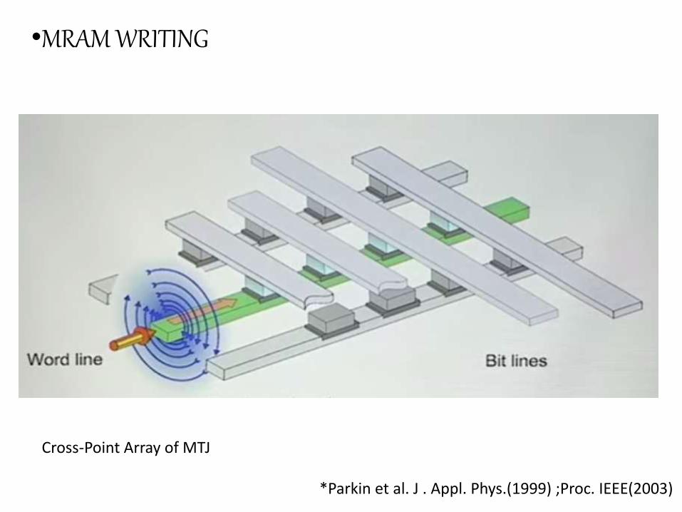
•MRAM WRITING
Cross-Point Array of MTJ
*Parkin et al. J . Appl. Phys.(1999) ;Proc. IEEE(2003)
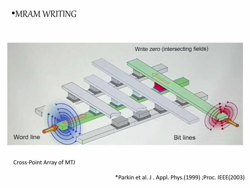
•MRAM WRITING
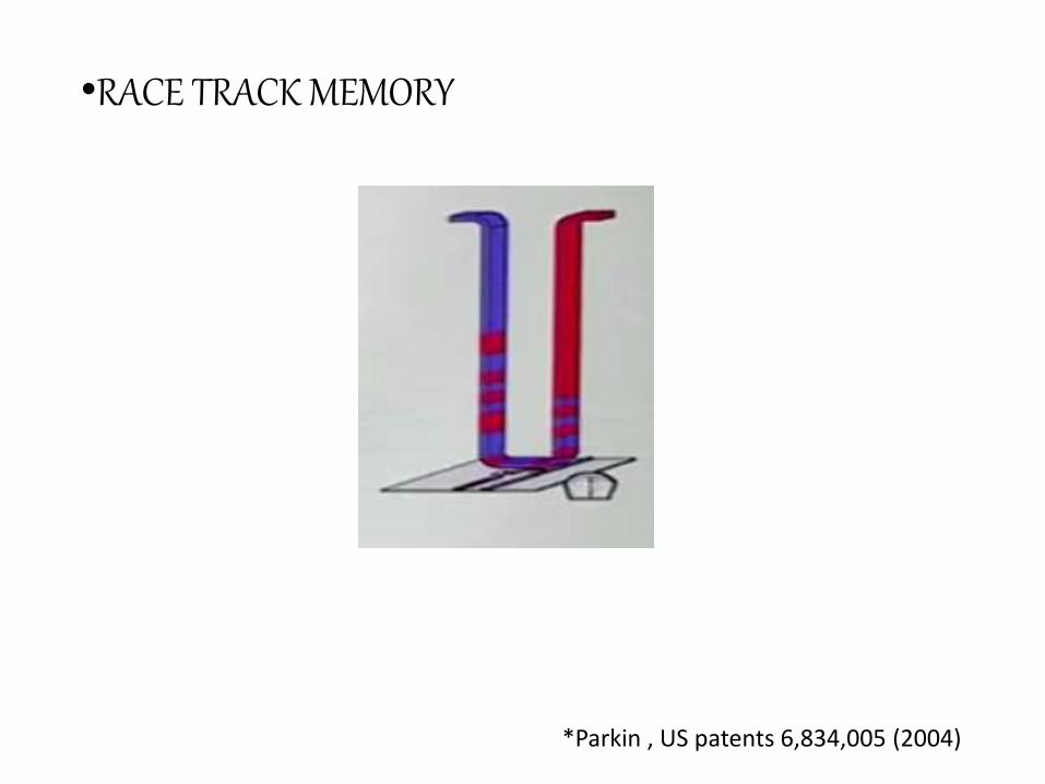
•RACE TRACK MEMORY
*Parkin , US patents 6,834,005 (2004)
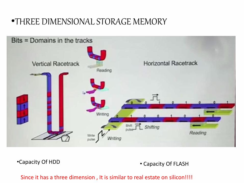
•THREE DIMENSIONAL STORAGE MEMORY
•Capacity Of HDD • Capacity Of FLASH
Since it has a three dimension , It is similar to real estate on silicon!!!!
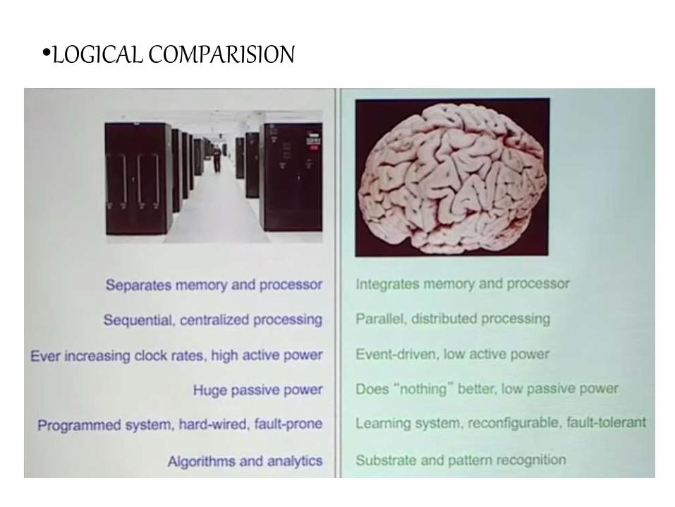
•LOGICAL COMPARISION
• ADVANTAGES
• Non Volatile
•Doesn’t require specific materials
•Speed
•Cost
• Advantage of Both electronics and Magnetics
• COnClUSION :
As said in the starting itself that it is a new era in electronics . That we can concludeFrom its advantages also.
By using all electronic and magnetic properties of charge this field open the door for many new invention and possibilities in future.

•REFERENCES

THANK YOU!!!


![Spintronics [EDocFind.com]](https://img.dokumen.tips/doc/110x75/577d2e0b1a28ab4e1eaea99b/spintronics-edocfindcom.jpg)