Embed Size (px)
Citation preview

Mon-Ren Chene, S2C Chairman and CTODecember 2010
Rapid SoC PrototypingShortens Time-to-Market

Getting to Market Early Can Be the Difference Between Success and Failure
• Design complexity is increasing• Market pressures are increasing
– Shorter product life cycles– World-wide competition
• The success of a project depends on:– The SoC having the right functionality– First pass silicon success
• Early prototyping– Validate SoC functionality– Create high performance software development platforms

SoC Software is the Fastest Growing Development Costs
SoC SoftwareSoC Software
Architecture, Design and Verification
Architecture, Design and Verification
Implementation & ManufacturingImplementation & Manufacturing
SoC Development Costs have Soared from $20 Million at 90nm to Over $100 Million at 32 nm
SoC Development Costs have Soared from $20 Million at 90nm to Over $100 Million at 32 nm
Source: IBSSource: IBS

SoC Prototyping Benefits
• Hardware Design– Early system validation
– Test in actual system
– Start chip design with proven system
• Software Development– Early software design
– Validate software in target system
– Fast software verification cycles
SoC Prototyping Gets You to Market Ahead of Your Competition!
SoC Prototyping Gets You to Market Ahead of Your Competition!

S2C is Focused on Rapid SoC Prototyping
New Vertical SoC Design Market Segmentation
“System Prototyping” is now the KEY!
We focus Here

S2C History
Transwitch IP Partner
1st Generation ProductIP Porter
2nd GenerationTAI Logic Module
2003 2004 2005 2006 2007 2008 2009 2010 2003 2004 2005 2006 2007 2008 2009 2010
Tensilica IP Partner
CAST IP Partner
3rd GenerationV5 TAI Logic Module
Northwest IP Partner
Founded in Silicon Valley
IPextreme IP Partner
Ittiam IP Partner
Established R&D Center in Shanghai
4th GenerationS4/V6 TAI Logic Module
Host 3rd SoCIP Conference
Host 2nd SoCIP
Conference
Host 1st SoCIPConference
CosmicIP Partner
Allegro IP Partner

Prototyping Tools Silicon IP
Prototyping HardwareIP Porter
Xilinx V4 TAI Logic ModuleXilinx V5 TAI Logic ModuleXilinx V6 TAI Logic ModuleAltera S4 TAI Logic Module
Digital IPProcessors
CommunicationsMultimedia
Memory ControllerEncryption Wireless
Peripherals
On-Line MediaIndustry Trends and News
IP and SoC technologySoC design resources
Prototyping SoftwareTAI Player ProTAI Compiler
TAI SimX
Analog IPAD/DA, PLL
PHY etc
Partner ProgramPrototype-Ready IP Partnership
Standardized Prototyping Platform Prototype Ready IP Effective Ecosystem
SoCIP Portal
S2C’s Main Business Units
EventsSoCIP annual conference
Series of Road show

Comprehensive SoC Prototyping Solutions
1) FPGA Prototyping Hardware TAI Logic Module
2) FPGA Prototyping Software TAI Player Pro
3) Prototype Ready IP TAI IP Library

S2C’s 4th Generation High Performance and Reliability Hardware
• Power Management– Up to 50A current for FPGA core– Up to 10W power for FPGA I/O– FPGA current, voltage and temperature monitor and protect– Dynamically adjust current and voltage safety threshold
• Noise Shielding– Isolated power modules– 50 Ohm impedance match for each single ended FPGA I/O– 100 Ohm impedance match for each pair of LVDS FPGA I/O
• High-Speed PCB Simulation – Performed by the leading PCB design house, Japan Circuit,
in Japan

Flexible I/O Voltage
• Dedicated I/O – Individually adjustable to 1.2V, 1.8V, 2.5V or 3.0V for each
connector
– Other voltage settings can also be adjusted via changing resistors
• Shared I/O– Adjustable to 2.5V or 3.0V
Adjustable I/O Voltage Switch

Advanced Clock Management
• 20 user clocks from– 2 oscillator sockets
– 3 pairs of differential SMB clock inputs
– 3 programmable clock source (1~195MHz)
– 12 feedback clocks from any user FPGA
– 12 clock sources from TAI Pod connector
F1 F2
LM Controller
Spartan
2 OSC Sockets
3 SMB Inputs
3 Programmable Clocks
20
12 Feedbacks
Feedback I/O connector to/from other boards

Stackable Architecture
240 Dedicated I/O
240 Dedicated I/O
454 (382 for 530)Shared Nets & I/O
TAI LM 1
240 Dedicated I/O
240 Dedicated I/O
TAI LM 2
240 Dedicated I/O
240 Dedicated I/O
TAI LM 3
F1 F2
F1 F2
F1 F2
176 (120 for 530)Shared I/O
176 (120 for 530)Shared I/O
176 (120 for 530)Shared I/O
176 (120 for 530)Shared I/O

Expandable Through Mother Board
F1 F2416
(360 for 530) Dedicated I/O
User Defined
TAI LM 1
F1 F2
TAI LM 2
Mother Board
416(360 for 530) Dedicated I/O
416(360 for 530) Dedicated I/O
416(360 for 530) Dedicated I/O

• Up to 16.4 million ASIC gates on one board
• Up to 60 million bits of FPGA internal memories
• One on-board DDR2 SO-DIMM socket
• One on-board DDR3 SO-DIMM socket
Easily stackable to accommodate even larger designs!
Dual Stratix-4 TAI Logic Module
Prototyping Hardware – Stratix-4 TAI Logic Module

Stratix-4 TAI Logic Module Products
Dual SingleA SingleB
Dual4S820
Dual4S530
Single 4S820A
Single 4S530A
Single 4S820B
Single 4S530B
Logic Capacity (ASIC Gates)
16.4M 10.6M 8.2M 5.3M 8.2M 5.3M
FPGA Memory 66Mbits 54Mbits 35Mbits 27Mbits 35Mbits 27Mbits
On-Board Memory
2GByte DDR3
2GByte DDR2
2GByte DDR3
2GByte DDR2
2GByte DDR3
2GByte DDR3
2GByte DDR2
2GByte DDR2
External User IO
1286 1102 870 742 870 742
Inter-FPGA Nets
454 382 N/A N/A N/A N/A
User Clocks 20 20 20 20 20 20

• Up to 15.2 million ASIC gates on one board
• Up to 50 million bits of FPGA internal memories
• One on-board DDR2 SO-DIMM socket
• One on-board DDR3 SO-DIMM socket
Easily stackable to accommodate even larger designs!
Dual Virtex 6 TAI Logic Module
Prototyping Hardware – Virtex 6 TAI Logic Module

S2C Virtex-6 TAI LM Products
Dual SingleA SingleB
Dual6V760
Dual6V550
Single 6V760A
Single 6V550A
Single 6V760B
Single 6V550B
Logic Capacity (ASIC Gates)
15.2M 11M 7.6M 5.5M 7.6M 5.5M
FPGA Memory
50Mbits 44Mbits 25Mbits 22Mbits 25Mbits 22Mbits
On-Board Memory
2GByte DDR3
2GByte DDR2
2GByte DDR3
2GByte DDR2
2GByte DDR3
2GByte DDR3
2GByte DDR2
2GByte DDR2
External User IO
1260 1260 900 900 900 900
Inter-FPGA Nets
540 540 N/A N/A N/A N/A
User Clocks 16 16 16 16 16 16

S2C TAI Logic Modules
TAI Logic Modules
Single Dual Quad Comments
Altera
Stratix 4 820E ✔ Dec. 2010
Stratix 4 530E ✔ Dec 2010
Stratix 4 820E ✔ ✔
Stratix 4 530E ✔ ✔
Xilinx
Virtex 6-760 ✔ ✔
Virtex 6-550 ✔ ✔
Virtex 5-330 ✔ ✔
Virtex 5-220 ✔
Virtex 5-110 ✔
SingleSingle
DualDual
StackedStacked

Mictor InterfaceProcessorPeripheral
DVI Input Interface
TAI LM Expansion with Daughter Cards
TAI LM Expansion with Mother Board
9MB SRAM 2 Channel 128MB DDR
DVI OutputInterface
Gigabit Ethernet PHY Interface
PCIe 1-Lane PHY Interface
TV Decoder TV Encoder
GPIO Interface
Audio Interface
MS/SD/XD Interface
Multifunctional Memory
Plug-and-Play TAI LM Accessories Modules

Compilation/Partition USB Download/Control
Pin Assignment
Self Test
Clock ManagementDebug
TAI Player Pro – Prototype Automation Software

Prototype Ready™ IP – Pre-Engineered for Your Success
• Prototype Ready IP– Develop & test reference
design on TAI LM– Plug & Play in Prototyping
System
Accelerating SoC design!!!

Prototype Ready™ IP
• Complexity ranges from 2 IP blocks to entire hardware platforms• Enables SoC design to focus on system design• Altera Stratix 4 based DDR2/3 Prototype Ready IP
– Includes DDR2 SDRAM operating at 533Mbps and DDR3 SDRAM operating at 800Mbps.
– Utilizes Altera Stratix series external memory interface resources
• CAST H.264/PCIe Prototype Ready IP• Northwest Logic DDR2/DDR3 Prototype Ready IP• Tensilica CPU/DSP• More Prototype IP and platforms to be announce in 2011
Pre-Engineered for Your Success!Pre-Engineered for Your Success!

IP Partners

S2C Customers

SoCIP Platform – SoC Design Technology Portal
• Complete IP offering from SoCIP partners with focus on Prototype Ready IP
• Your source of SoC Design and IP news and products www.socip.org
• Meet IP and SoC design experts at SoCIP conferences & Road Shows
• Contact S2C for sponsorship opportunities
Register your email at [email protected] to get free SoCIP newsletter

SoCIP Conferences
2010 Gold Sponsors: 2010 Gold Sponsors:
2010 Silver Sponsors: 2010 Silver Sponsors:
3 Years of Success!!!SoCIP 2008 ~2010
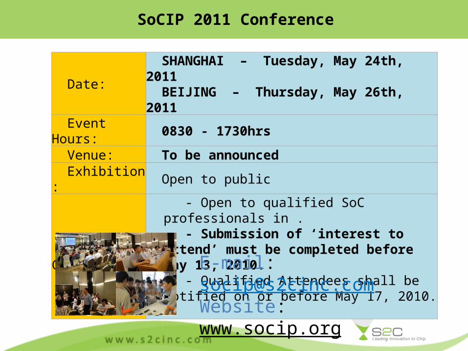
Date: SHANGHAI – Tuesday, May 24th, 2011 BEIJING – Thursday, May 26th, 2011
Event Hours: 0830 - 1730hrs Venue: To be announced Exhibition: Open to public
Conference:
- Open to qualified SoC professionals in . - Submission of ‘interest to attend’ must be completed
before May 13, 2010. - Qualified Attendees shall be notified on or before May
17, 2010.
SoCIP 2011 Conference
E-mail: [email protected]: www.socip.org

Summary
Prototyping Tools
Standardized Prototyping
Platform
Silicon IP
Prototype Ready IPEffective
Ecosystem
SoCIP Portal

Thank You
USA
1754 Technology Drive
Suite 206, San Jose, CA 95110, USA
Tel: +1 408 213 8818
Fax: +1 408 213 8821
北京 北京市海淀区大钟寺东路太阳园 3 号楼1403 室邮编: 100086
电话: +86 -10 -8212 2630
传真: +86 -10 -8212 2030
上海 上海浦东南路 855 号世界广场 15J
邮编: 200120
电话 : : +86 -21 -6887 9287
传真: +86 -21 -6887 9289
深圳 深圳市福田区商报路 7 号天健公寓 803
邮编: 518034
电话: +86 -755 -2676 6711
传真: +86 -755 -2676 6711
Contact: [email protected]