Embed Size (px)
Citation preview

144
C H A P T E R
5
T H E C M O S I N V E R T E R
Quantification of integrity, performance, and energy metrics of an inverterOptimization of an inverter design
5.1 Introduction
5.2 The Static CMOS Inverter — An Intuitive Perspective
5.3 Evaluating the Robustness of the CMOS Inverter: The Static Behavior
5.3.1 Switching Threshold
5.3.2 Noise Margins
5.3.3 Robustness Revisited
5.4 Performance of CMOS Inverter: The Dynamic Behavior
5.4.1 Computing the Capacitances
5.4.2 Propagation Delay: First-Order Analysis
5.4.3 Propagation Delay Revisited
5.5 Power, Energy, and Energy-Delay
5.5.1 Dynamic Power Consumption
5.5.2 Static Consumption
5.5.3 Putting It All Together
5.5.4 Analyzing Power Consumption Using SPICE
5.6 Perspective: Technology Scaling and its Impact on the Inverter Metrics
chapter5.fm Page 144 Monday, September 6, 1999 11:41 AM

Section 5.1 Introduction 145
5.1 Introduction
The inverter is truly the nucleus of all digital designs. Once its operation and properties areclearly understood, designing more intricate structures such as NAND gates, adders, mul-tipliers, and microprocessors is greatly simplified. The electrical behavior of these com-plex circuits can be almost completely derived by extrapolating the results obtained forinverters. The analysis of inverters can be extended to explain the behavior of more com-plex gates such as NAND, NOR, or XOR, which in turn form the building blocks for mod-ules such as multipliers and processors.
In this chapter, we focus on one single incarnation of the inverter gate, being thestatic CMOS inverter — or the CMOS inverter, in short. This is certainly the most popularat present, and therefore deserves our special attention. We analyze the gate with respectto the different design metrics that were outlined in Chapter 1:
• cost, expressed by the complexity and area
• integrity and robustness, expressed by the static (or steady-state) behavior
• performance, determined by the dynamic (or transient) response
• energy efficiency, set by the energy and power consumption
From this analysis arises a model of the gate that will help us to identify the parame-ters of the gate and to choose their values so that the resulting design meets desired speci-fications. While each of these parameters can be easily quantified for a given technology,we also discuss how they are affected by scaling of the technology.
While this Chapter focuses uniquely on the CMOS inverter, we will see in the fol-lowing Chapter that the same methodology also applies to other gate topologies.
5.2 The Static CMOS Inverter — An Intuitive Perspective
Figure 5.1 shows the circuit diagram of a static CMOS inverter. Its operation is readilyunderstood with the aid of the simple switch model of the MOS transistor, introduced inChapter 3 (Figure 3.25): the transistor is nothing more than a switch with an infinite off-resistance (for |VGS| < |VT|), and a finite on-resistance (for |VGS| > |VT|). This leads to the
VDD
Vin Vout
CL
Figure 5.1 Static CMOS inverter. VDD stands for the supply voltage.
chapter5.fm Page 145 Monday, September 6, 1999 11:41 AM

146 THE CMOS INVERTER Chapter 5
following interpretation of the inverter. When Vin is high and equal to VDD, the NMOStransistor is on, while the PMOS is off. This yields the equivalent circuit of Figure 5.2a. Adirect path exists between Vout and the ground node, resulting in a steady-state value of 0V. On the other hand, when the input voltage is low (0 V), NMOS and PMOS transistorsare off and on, respectively. The equivalent circuit of Figure 5.2b shows that a path existsbetween VDD and Vout, yielding a high output voltage. The gate clearly functions as aninverter.
A number of other important properties of static CMOS can be derived from this switch-level view:
• The high and low output levels equal VDD and GND, respectively; in other words,the voltage swing is equal to the supply voltage. This results in high noise margins.
• The logic levels are not dependent upon the relative device sizes, so that the transis-tors can be minimum size. Gates with this property are called ratioless. This is incontrast with ratioed logic, where logic levels are determined by the relative dimen-sions of the composing transistors.
• In steady state, there always exists a path with finite resistance between the outputand either VDD or GND. A well-designed CMOS inverter, therefore, has a low out-put impedance, which makes it less sensitive to noise and disturbances. Typical val-ues of the output resistance are in kΩ range.
• The input resistance of the CMOS inverter is extremely high, as the gate of an MOStransistor is a virtually perfect insulator and draws no dc input current. Since theinput node of the inverter only connects to transistor gates, the steady-state inputcurrent is nearly zero. A single inverter can theoretically drive an infinite number ofgates (or have an infinite fan-out) and still be functionally operational; however,increasing the fan-out also increases the propagation delay, as will become clearbelow. So, although fan-out does not have any effect on the steady-state behavior, itdegrades the transient response.
Figure 5.2 Switch models of CMOS inverter.
VDD VDD
VoutVout
Vin = VDD Vin = 0
Rn
Rp
(a) Model for high input (b) Model for low input
chapter5.fm Page 146 Monday, September 6, 1999 11:41 AM

Section 5.2 The Static CMOS Inverter — An Intuitive Perspective 147
• No direct path exists between the supply and ground rails under steady-state operat-ing conditions (this is, when the input and outputs remain constant). The absence ofcurrent flow (ignoring leakage currents) means that the gate does not consume anystatic power.
SIDELINE: The above observation, while seemingly obvious, is of crucial importance,and is one of the primary reasons CMOS is the digital technology of choice at present. Thesituation was very different in the 1970s and early 1980s. All early microprocessors, suchas the Intel 4004, were implemented in a pure NMOS technology. The lack of comple-mentary devices (such as the NMOS and PMOS transistor) in such a technology makesthe realization of inverters with zero static power non-trivial. The resulting static powerconsumption puts a firm upper bound on the number of gates that can be integrated on asingle die; hence the forced move to CMOS in the 1980s, when scaling of the technologyallowed for higher integration densities.
The nature and the form of the voltage-transfer characteristic (VTC) can be graphi-cally deduced by superimposing the current characteristics of the NMOS and the PMOSdevices. Such a graphical construction is traditionally called a load-line plot. It requiresthat the I-V curves of the NMOS and PMOS devices are transformed onto a common coor-dinate set. We have selected the input voltage Vin, the output voltage Vout and the NMOSdrain current IDN as the variables of choice. The PMOS I-V relations can be translated intothis variable space by the following relations (the subscripts n and p denote the NMOSand PMOS devices, respectively):
(5.1)
The load-line curves of the PMOS device are obtained by a mirroring around the x-axis and a horizontal shift over VDD. This procedure is outlined in Figure 5.3, where thesubsequent steps to adjust the original PMOS I-V curves to the common coordinate set Vin,Vout and IDn are illustrated.
IDSp IDSn–=
VGSn Vin VGSp; Vin VDD–= =
VDSn Vout VDSp; Vout VDD–= =
VDSp
IDp
VGSp = –2.5
VGSp = –1VDSp
IDnVin = 0
Vin = 1.5
Vout
IDnVin = 0
Vin = 1.5
Vin = VDD + VGSpIDn = –IDp
Vout = VDD + VDSp
Figure 5.3 Transforming PMOS I-V characteristic to a common coordinate set (assuming VDD = 2.5 V).
chapter5.fm Page 147 Monday, September 6, 1999 11:41 AM

148 THE CMOS INVERTER Chapter 5
The resulting load lines are plotted in Figure 5.4. For a dc operating points to bevalid, the currents through the NMOS and PMOS devices must be equal. Graphically, thismeans that the dc points must be located at the intersection of corresponding load lines. Anumber of those points (for Vin = 0, 0.5, 1, 1.5, 2, and 2.5 V) are marked on the graph. Ascan be observed, all operating points are located either at the high or low output levels.The VTC of the inverter hence exhibits a very narrow transition zone. This results fromthe high gain during the switching transient, when both NMOS and PMOS are simulta-neously on, and in saturation. In that operation region, a small change in the input voltageresults in a large output variation. All these observations translate into the VTC of Figure5.5.
Before going into the analytical details of the operation of the CMOS inverter, aqualitative analysis of the transient behavior of the gate is appropriate as well. Thisresponse is dominated mainly by the output capacitance of the gate, CL, which is com-
Figure 5.4 Load curves for NMOS and PMOS transistors of the static CMOS inverter (VDD = 2.5 V). The dotsrepresent the dc operation points for various input voltages.
IDn
Vout
Vin = 2.5
Vin = 2
Vin = 1.5
Vin = 0
Vin = 0.5
Vin = 1
NMOS
Vin = 0
Vin = 0.5
Vin = 1Vin = 1.5
Vin = 2
Vin = 2.5
Vin = 1Vin = 1.5
PMOS
Vout
Vin0.5 1 1.5 2 2.5
0.5
11.
52
2.5
Figure 5.5 VTC of static CMOS inverter, derived from Figure 5.4 (VDD = 2.5 V). For each operation region, the modes of the transistors are annotated — off, res(istive), or sat(urated).
NMOS resPMOS off
NMOS satPMOS sat
NMOS offPMOS res
NMOS satPMOS res
NMOS resPMOS sat
chapter5.fm Page 148 Monday, September 6, 1999 11:41 AM

Section 5.3 Evaluating the Robustness of the CMOS Inverter: The Static Behavior 149
posed of the drain diffusion capacitances of the NMOS and PMOS transistors, the capaci-tance of the connecting wires, and the input capacitance of the fan-out gates. Assumingtemporarily that the transistors switch instantaneously, we can get an approximate idea ofthe transient response by using the simplified switch model again (Figure 5.6). Let us con-sider the low-to-high transition first (Figure 5.6a). The gate response time is simply deter-mined by the time it takes to charge the capacitor CL through the resistor Rp. In Example4.5, we learned that the propagation delay of such a network is proportional to the its time-constant RpCL. Hence, a fast gate is built either by keeping the output capacitancesmall or by decreasing the on-resistance of the transistor. The latter is achieved byincreasing the W/L ratio of the device. Similar considerations are valid for the high-to-lowtransition (Figure 5.6b), which is dominated by the RnCL time-constant. The reader shouldbe aware that the on-resistance of the NMOS and PMOS transistor is not constant, but is anonlinear function of the voltage across the transistor. This complicates the exact determi-nation of the propagation delay. An in-depth analysis of how to analyze and optimize theperformance of the static CMOS inverter is offered in Section 5.4.
5.3 Evaluating the Robustness of the CMOS Inverter: The Static Behavior
In the qualitative discussion above, the overall shape of the voltage-transfer characteristicof the static CMOS inverter was derived, as were the values of VOH and VOL (VDD andGND, respectively). It remains to determine the precise values of VM, VIH, and VIL as wellas the noise margins.
5.3.1 Switching Threshold
The switching threshold, VM, is defined as the point where Vin = Vout. Its value can beobtained graphically from the intersection of the VTC with the line given by Vin = Vout(see Figure 5.5). In this region, both PMOS and NMOS are always saturated, since VDS =VGS. An analytical expression for VM is obtained by equating the currents through the tran-
VDDVDD
Vout
Vin = VDDVin = 0
Rp
Rn
Vout
CLCL
(a) Low-to-high (b) High-to-low
Figure 5.6 Switch model of dynamic behavior of static CMOS inverter.
chapter5.fm Page 149 Monday, September 6, 1999 11:41 AM

150 THE CMOS INVERTER Chapter 5
sistors. We solve the case where the supply voltage is high so that the devices can beassumed to be velocity-saturated (or VDSAT < VM - VT). We furthermore ignore the channel-length modulation effects.
(5.2)
Solving for VM yields
(5.3)
assuming identical oxide thicknesses for PMOS and NMOS transistors. For large valuesof VDD (compared to threshold and saturation voltages), Eq. (5.3) can be simplified:
(5.4)
Eq. (5.4) states that the switching threshold is set by the ratio r, which compares the rela-tive driving strengths of the PMOS and NMOS transistors. It is generally considered to bedesirable for VM to be located around the middle of the available voltage swing (or atVDD/2), since this results in comparable values for the low and high noise margins. Thisrequires r to be approximately 1, which is equivalent to sizing the PMOS device so that(W/L)p = (W/L)n × (VDSATnk′n )/(VDSATnk′p ). To move VM upwards, a larger value of r isrequired, which means making the PMOS wider. Increasing the strength of the NMOS, onthe other hand, moves the switching threshold closer to GND.
From Eq. (5.2), we can derive the required ratio of PMOS versus NMOS transistorsizes such that the switching threshold is set to a desired value VM. When using thisexpression, please make sure that the assumption that both devices are velocity-saturatedstill holds for the chosen operation point.
(5.5)
Problem 5.1 Inverter switching threshold for long-channel devices, or low supply-volt-ages.
The above expressions were derived under the assumption that the transistors are velocity-saturated. When the PMOS and NMOS are long-channel devices, or when the supply volt-age is low, velocity saturation does not occur (VM-VT < VDSAT). Under these circumstances,Eq. (5.6) holds for VM. Derive.
(5.6)
knVDSATn VM VTn–VDSATn
2-----------------–
kpVDSATp VM VDD VTp––VDSATp
2-----------------–
+ 0=
VM
VTnVDSATn
2-----------------+
r VDD V+ TpVDSATp
2-----------------+
+
1 r+----------------------------------------------------------------------------------------------------- with r
kpVDSATp
knVDSATn----------------------
υsatpWp
υsatnWn-------------------= ==
VMrVDD
1 r+------------≈
W L⁄( )p
W L⁄( )n-------------------
k′nVDSATn VM VTn– VDSATn 2⁄–( )k′pVDSATp VDD V– M VTp VDSATp 2⁄+ +( )---------------------------------------------------------------------------------------------------=
VMVTn r VDD V+ Tp( )+
1 r+----------------------------------------------- with = r
kp–kn
--------=
chapter5.fm Page 150 Monday, September 6, 1999 11:41 AM

Section 5.3 Evaluating the Robustness of the CMOS Inverter: The Static Behavior 151
When designing static CMOS circuits, it is advisable to balance the driving strengths of thetransistors by making the PMOS section wider than the NMOS section, if one wants to maxi-mize the noise margins and obtain symmetrical characteristics. The required ratio is given byEq. (5.5).
Example 5.1 Switching threshold of CMOS inverter
We derive the sizes of PMOS and NMOS transistors such that the switching threshold of aCMOS inverter, implemented in our generic 0.25 µm CMOS process, is located in the middlebetween the supply rails. We use the process parameters presented in Example 3.7, andassume a supply voltage of 2.5 V. The minimum size device has a width/length ratio of 1.5.With the aid of Eq. (5.5), we find
Figure 5.7 plots the values of switching threshold as a function of the PMOS/NMOSratio, as obtained by circuit simulation. The simulated PMOS/NMOS ratio of 3.4 for a 1.25 Vswitching threshold confirms the value predicted by Eq. (5.5).
An analysis of the curve of Figure 5.7 produces some interesting observations:
1. VM is relatively insensitive to variations in the device ratio. This means that smallvariations of the ratio (e.g., making it 3 or 2.5) do not disturb the transfer character-istic that much. It is therefore an accepted practice in industrial designs to set thewidth of the PMOS transistor to values smaller than those required for exact sym-metry. For the above example, setting the ratio to 3, 2.5, and 2 yields switchingthresholds of 1.22 V, 1.18 V, and 1.13 V, respectively.
Design Technique — Maximizing the noise margins
W L⁄( )p
W L⁄( )n------------------- 115 10 6–×
30 10 6–×------------------------- 0.63
1.0---------- 1.25 0.43 0.63 2⁄––( )
1.25 0.4 1.0 2⁄––( )-------------------------------------------------------×× 3.5= =
Figure 5.7 Simulated inverter switching threshold versus PMOS/NMOS ratio (0.25 µm CMOS, VDD = 2.5 V)
100
101
0.8
0.9
1
1.1
1.2
1.3
1.4
1.5
1.6
1.7
1.8
VM
(V)
Wp/W
n
chapter5.fm Page 151 Monday, September 6, 1999 11:41 AM

152 THE CMOS INVERTER Chapter 5
2. The effect of changing the Wp/Wn ratio is to shift the transient region of the VTC.Increasing the width of the PMOS or the NMOS moves VM towards VDD or GNDrespectively. This property can be very useful, as asymmetrical transfer characteris-tics are actually desirable in some designs. This is demonstrated by the example ofFigure 5.8. The incoming signal Vin has a very noisy zero value. Passing this signalthrough a symmetrical inverter would lead to erroneous values (Figure 5.8a). Thiscan be addressed by raising the threshold of the inverter, which results in a correctresponse (Figure 5.8b). Further in the text, we will see other circuit instances whereinverters with asymetrical switching thresholds are desirable.Changing the switching threshold by a considerable amount is however not easy,especially when the ratio of supply voltage to transistor threshold is relatively small(2.5/0.4 = 6 for our particular example). To move the threshold to 1.5 V requires atransistor ratio of 11, and further increases are prohibitively expensive. Observe thatFigure 5.7 is plotted in a semilog format.
5.3.2 Noise Margins
By definition, VIH and VIL are the operational points of the inverter where . In
the terminology of the analog circuit designer, these are the points where the gain g of theamplifier, formed by the inverter, is equal to − 1. While it is indeed possible to derive ana-lytical expressions for VIH and VIL, these tend to be unwieldy and provide little insight inwhat parameters are instrumental in setting the noise margins.
A simpler approach is to use a piecewise linear approximation for the VTC, asshown in Figure 5.9. The transition region is approximated by a straight line, the gain ofwhich equals the gain g at the switching threshold VM. The crossover with the VOH and theVOL lines is used to define VIH and VIL points. The error introduced is small and well
Figure 5.8 Changing the inverter threshold can improve the circuit reliability.
Vin
t
t t
Vin Vout
VoutVout
Vmb
Vma
(a) Response of standard inverter
b) Response of inverter with modified threshold
V inddVout 1–=
chapter5.fm Page 152 Monday, September 6, 1999 11:41 AM
Section 5.3 Evaluating the Robustness of the CMOS Inverter: The Static Behavior 153
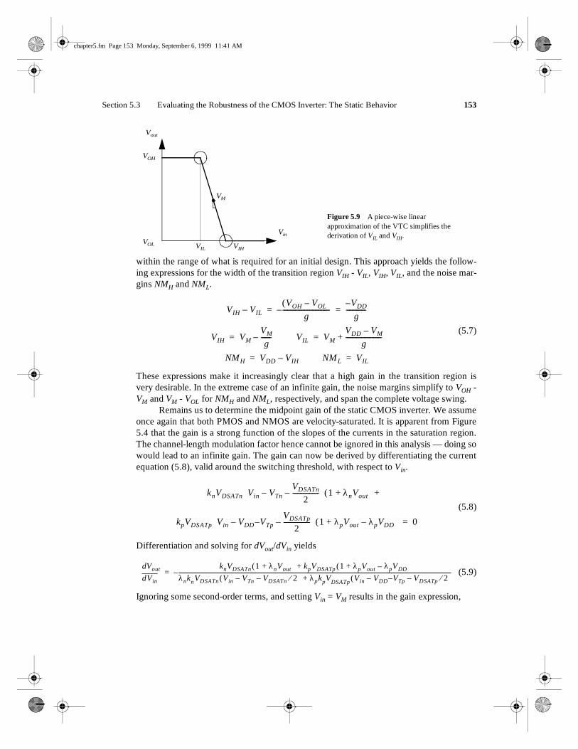
within the range of what is required for an initial design. This approach yields the follow-ing expressions for the width of the transition region VIH - VIL, VIH, VIL, and the noise mar-gins NMH and NML.
(5.7)
These expressions make it increasingly clear that a high gain in the transition region isvery desirable. In the extreme case of an infinite gain, the noise margins simplify to VOH -VM and VM - VOL for NMH and NML, respectively, and span the complete voltage swing.
Remains us to determine the midpoint gain of the static CMOS inverter. We assumeonce again that both PMOS and NMOS are velocity-saturated. It is apparent from Figure5.4 that the gain is a strong function of the slopes of the currents in the saturation region.The channel-length modulation factor hence cannot be ignored in this analysis — doing sowould lead to an infinite gain. The gain can now be derived by differentiating the currentequation (5.8), valid around the switching threshold, with respect to Vin.
(5.8)
Differentiation and solving for dVout/dVin yields
(5.9)
Ignoring some second-order terms, and setting Vin = VM results in the gain expression,
VOH
VOL
Vin
Vout
VM
VIL VIH
Figure 5.9 A piece-wise linear approximation of the VTC simplifies the derivation of VIL and VIH.
VIH VIL–VOH VOL–( )
g------------------------------–
VDD–g
-------------= =
VIH VMVM
g-------–= VIL VM
VDD VM–g
-----------------------+=
NMH VDD VIH–= NM L VIL=
knVDSATn Vin VTn–VDSATn
2-----------------–
1 λnVout+( )+
kpVDSATp Vin VDD VTp––VDSATp
2-----------------–
1 λpVout λpVDD–+( ) 0=
VinddVout knVDSATn 1 λnVout+( ) kpVDSATp 1 λpVout λpVDD–+( )+
λnknVDSATn Vin VTn– VDSATn 2⁄–( ) λpkpVDSATp V in VDD VTp–– VDSATp 2⁄–( )+------------------------------------------------------------------------------------------------------------------------------------------------------------------------------------------------–=
chapter5.fm Page 153 Monday, September 6, 1999 11:41 AM

154 THE CMOS INVERTER Chapter 5
(5.10)
with ID(VM) the current flowing through the inverter for Vin = VM. The gain is almostpurely determined by technology parameters, especially the channel length modulation. Itcan only in a minor way be influenced by the designer through the choice of supply andswitching threshold voltages.
Example 5.2 Voltage transfer characteristic and noise margins of CMOS Inverter
Assume an inverter in the generic 0.25 µm CMOS technology designed with a PMOS/NMOSratio of 3.4 and with the NMOS transistor minimum size (W = 0.375 µm, L = 0.25 µm, W/L =1.5). We first compute the gain at VM (= 1.25 V),
This yields the following values for VIL, VIH, NML, NMH:
VIL = 1.2 V, VIH = 1.3 V, NML = NMH = 1.2.
Figure 5.10 plots the simulated VTC of the inverter, as well as its derivative, the gain. A closeto ideal characteristic is obtained. The actual values of VIL and VIH are 1.03 V and 1.45 V,respectively, which leads to noise margins of 1.03 V and 1.05 V. These values are lower thanthose predicted for two reasons:
• Eq. (5.10) overestimates the gain. As observed in Figure 5.10b, the maximum gain (atVM) equals only 17. This reduced gain would yield values for VIL and VIH of 1.17 V, and 1.33V, respectively.
• The most important deviation is due to the piecewise linear approximation of theVTC, which is optimistic with respect to the actual noise margins.
The obtained expressions are however perfectly useful as first-order estimations aswell as means of identifying the relevant parameters and their impact.
To conclude this example, we also extracted from simulations the output resistance ofthe inverter in the low- and high-output states. Low values of 2.4 kΩ and 3.3 kΩ wereobserved, respectively. The output resistance is a good measure of the sensitivity of the gatein respect to noise induced at the output, and is preferably as low as possible.
SIDELINE: Surprisingly (or not so surprisingly), the static CMOS inverter can also beused as an analog amplifier, as it has a fairly high gain in its transition region. This regionis very narrow however, as is apparent in the graph of Figure 5.10b. It also receives poormarks on other amplifier properties such as supply noise rejection. Yet, this observationcan be used to demonstrate one of the major differences between analog and digitaldesign. Where the analog designer would bias the amplifier in the middle of the transientregion, so that a maximum linearity is obtained, the digital designer will operate the
g 1ID VM( )-----------------–
knVDSATn kpVDSATp+λn λp–
---------------------------------------------------=
1 r+VM VTn– VDSATn 2⁄–( ) λn λp–( )
-------------------------------------------------------------------------------≈
ID VM( ) 1.5 115 10 6–×× 0.63 1.25 0.43– 0.63 2⁄–( ) 1 0.06 1.25×+( )××× 59 10 6–× A= =
g 159 10 6–×---------------------- 1.5 115× 10 6–× 0.63× 1.5 3.4 30×× 10 6–× 1.0×+
0.06 0.1+-------------------------------------------------------------------------------------------------------------------------------– 27.5 (Eq. 5.10)–= =
chapter5.fm Page 154 Monday, September 6, 1999 11:41 AM

Section 5.3 Evaluating the Robustness of the CMOS Inverter: The Static Behavior 155
device in the regions of extreme nonlinearity, resulting in well-defined and well-separatedhigh and low signals.
Problem 5.2 Inverter noise margins for long-channel devices
Derive expressions for the gain and noise margins assuming that PMOS and NMOS arelong-channel devices (or that the supply voltage is low), so that velocity saturation doesnot occur.
5.3.3 Robustness Revisited
Device Variations
While we design a gate for nominal operation conditions and typical device parameters,we should always be aware that the actual operating temperature might very over a largerange, and that the device parameters after fabrication probably will deviate from the nom-inal values we used in our design optimization process. Fortunately, the dc-characteristicsof the static CMOS inverter turn out to be rather insensitive to these variations, and thegate remains functional over a wide range of operating conditions. This already becameapparent in Figure 5.7, which shows that variations in the device sizes have only a minorimpact on the switching threshold of the inverter. To further confirm the assumed robust-ness of the gate, we have re-simulated the voltage transfer characteristic by replacing thenominal devices by their worst- or best-case incarnations. Two corner-cases are plotted inFigure 5.11: a better-than-expected NMOS combined with an inferior PMOS, and theopposite scenario. Comparing the resulting curves with the nominal response shows thatthe variations mostly cause a shift in the switching threshold, but that the operation of the
0 0.5 1 1.5 2 2.50
0.5
1
1.5
2
2.5
Vin (V)
Vou
t(V)
0 0.5 1 1.5 2 2.5-18
-16
-14
-12
-10
-8
-6
-4
-2
0
Vin
(V)
gain
Figure 5.10 Simulated Voltage Transfer Characteristic (a) and voltage gain (b) of CMOS inverter (0.25 µm CMOS, VDD= 2.5 V).
(a) (b)
chapter5.fm Page 155 Monday, September 6, 1999 11:41 AM

156 THE CMOS INVERTER Chapter 5
gate is by no means affected. This robust behavior that ensures functionality of the gateover a wide range of conditions has contributed in a big way to the popularity of the staticCMOS gate.
Scaling the Supply Voltage
In Chapter 3, we observed that continuing technology scaling forces the supply voltages toreduce at rates similar to the device dimensions. At the same time, device threshold volt-ages are virtually kept constant. The reader probably wonders about the impact of thistrend on the integrity parameters of the CMOS inverter. Do inverters keep on workingwhen the voltages are scaled and are there potential limits to the supply scaling?
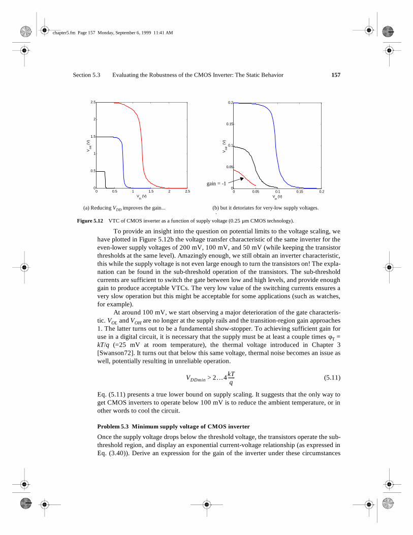
A first hint on what might happen was offered in Eq. (5.10), which indicates that thegain of the inverter in the transition region actually increases with a reduction of the sup-ply voltage! Note that for a fixed transistor ratio r, VM is approximately proportional toVDD. Plotting the (normalized) VTC for different supply voltages not only confirms thisconjecture, but even shows that the inverter is well and alive for supply voltages close tothe threshold voltage of the composing transistors (Figure 5.12a). At a voltage of 0.5 V —which is just 100 mV above the threshold of the transistors — the width of the transitionregion measures only 10% of the supply voltage (for a maximum gain of 35), while it wid-ens to 17% for 2.5 V. So, given this improvement in dc characteristics, why do we notchoose to operate all our digital circuits at these low supply voltages? Three importantarguments come to mind:
• In the following sections, we will learn that reducing the supply voltage indiscrimi-nately has a positive impact on the energy dissipation, but is absolutely detrimentalto the performance on the gate.
• The dc-characteristic becomes increasingly sensitive to variations in the deviceparameters such as the transistor threshold, once supply voltages and intrinsic volt-ages become comparable.
• Scaling the supply voltage means reducing the signal swing. While this typicallyhelps to reduce the internal noise in the system (such as caused by crosstalk), itmakes the design more sensitive to external noise sources that do not scale.
0 0.5 1 1.5 2 2.50
0.5
1
1.5
2
2.5
Vin
(V)
Vou
t(V)
Figure 5.11 Impact of device variations on static CMOS inverter VTC. The “good” device has a smaller oxide thickness (- 3nm), a smaller length (-25 nm), a higher width (+30 nm), and a smaller threshold (-60 mV). The opposite is true for the “bad” transistor.
Good NMOS Bad PMOS
Good PMOS Bad NMOS
Nominal
chapter5.fm Page 156 Monday, September 6, 1999 11:41 AM
Section 5.3 Evaluating the Robustness of the CMOS Inverter: The Static Behavior 157
To provide an insight into the question on potential limits to the voltage scaling, wehave plotted in Figure 5.12b the voltage transfer characteristic of the same inverter for theeven-lower supply voltages of 200 mV, 100 mV, and 50 mV (while keeping the transistorthresholds at the same level). Amazingly enough, we still obtain an inverter characteristic,this while the supply voltage is not even large enough to turn the transistors on! The expla-nation can be found in the sub-threshold operation of the transistors. The sub-thresholdcurrents are sufficient to switch the gate between low and high levels, and provide enoughgain to produce acceptable VTCs. The very low value of the switching currents ensures avery slow operation but this might be acceptable for some applications (such as watches,for example).
At around 100 mV, we start observing a major deterioration of the gate characteris-tic. VOL and VOH are no longer at the supply rails and the transition-region gain approaches1. The latter turns out to be a fundamental show-stopper. To achieving sufficient gain foruse in a digital circuit, it is necessary that the supply must be at least a couple times φΤ =kT/q (=25 mV at room temperature), the thermal voltage introduced in Chapter 3[Swanson72]. It turns out that below this same voltage, thermal noise becomes an issue aswell, potentially resulting in unreliable operation.
(5.11)
Eq. (5.11) presents a true lower bound on supply scaling. It suggests that the only way toget CMOS inverters to operate below 100 mV is to reduce the ambient temperature, or inother words to cool the circuit.
Problem 5.3 Minimum supply voltage of CMOS inverter
Once the supply voltage drops below the threshold voltage, the transistors operate the sub-threshold region, and display an exponential current-voltage relationship (as expressed inEq. (3.40)). Derive an expression for the gain of the inverter under these circumstances
0 0.05 0.1 0.15 0.20
0.05
0.1
0.15
0.2
Vin (V)
Vou
t (V)
Figure 5.12 VTC of CMOS inverter as a function of supply voltage (0.25 µm CMOS technology).
(a) Reducing VDD improves the gain...
0 0.5 1 1.5 2 2.50
0.5
1
1.5
2
2.5
Vin (V)
Vou
t(V)
. (b) but it detoriates for very-low supply voltages.
gain = -1
VDDmin 2… 4kTq
------>
chapter5.fm Page 157 Monday, September 6, 1999 11:41 AM

158 THE CMOS INVERTER Chapter 5
(assume symmetrical NMOS and PMOS transistors, and a maximum gain at VM = VDD/2).The resulting expression demonstrates that the minimum voltage is a function of the slopefactor n of the transistor.
(5.12)
According to this expression, the gain drops to -1 at VDD = 48 mV (for n = 1.5 and φT = 25mV).
5.4 Performance of CMOS Inverter: The Dynamic Behavior
The qualitative analysis presented earlier concluded that the propagation delay of theCMOS inverter is determined by the time it takes to charge and discharge the load capaci-tor CL through the PMOS and NMOS transistors, respectively. This observation suggeststhat getting CL as small as possible is crucial to the realization of high-performanceCMOS circuits. It is hence worthwhile to first study the major components of the loadcapacitance before embarking onto an in-depth analysis of the propagation delay of thegate. In addition to this detailed analysis, the section also presents a summary of tech-niques that a designer might use to optimize the performance of the inverter.
5.4.1 Computing the Capacitances
Manual analysis of MOS circuits where each capacitor is considered individually is virtu-ally impossible and is exacerbated by the many nonlinear capacitances in the MOS tran-sistor model. To make the analysis tractable, we assume that all capacitances are lumpedtogether into one single capacitor CL, located between Vout and GND. Be aware that this isa considerable simplification of the actual situation, even in the case of a simple inverter.
g 1n---
eVDD 2φT⁄
1–( )–=
VDD VDD
VinVout
M1
M2
M3
M4Cdb2
Cdb1
Cgd12
Cw
Cg4
Cg3
Figure 5.13 Parasitic capacitances, influencing the transient behavior of the cascaded inverter pair.
Vout2
chapter5.fm Page 158 Monday, September 6, 1999 11:41 AM

Section 5.4 Performance of CMOS Inverter: The Dynamic Behavior 159
Figure 5.13 shows the schematic of a cascaded inverter pair. It includes all thecapacitances influencing the transient response of node Vout. It is initially assumed that theinput Vin is driven by an ideal voltage source with zero rise and fall times. Accountingonly for capacitances connected to the output node, CL breaks down into the followingcomponents.
Gate-Drain Capacitance Cgd12
M1 and M2 are either in cut-off or in the saturation mode during the first half (up to 50%point) of the output transient. Under these circumstances, the only contributions to Cgd12are the overlap capacitances of both M1 and M2. The channel capacitance of the MOStransistors does not play a role here, as it is located either completely between gate andbulk (cut-off) or gate and source (saturation) (see Chapter 3).
The lumped capacitor model now requires that this floating gate-drain capacitor bereplaced by a capacitance-to-ground. This is accomplished by taking the so-called Millereffect into account. During a low-high or high-low transition, the terminals of the gate-drain capacitor are moving in opposite directions (Figure 5.14). The voltage change overthe floating capacitor is hence twice the actual output voltage swing. To present an identi-cal load to the output node, the capacitance-to-ground must have a value that is twice aslarge as the floating capacitance.
We use the following equation for the gate-drain capacitors: Cgd = 2 CGD0W (withCGD0 the overlap capacitance per unit width as used in the SPICE model). For an in-depthdiscussion of the Miller effect, please refer to textbooks such as Sedra and Smith([Sedra87], p. 57).1
Diffusion Capacitances Cdb1 and Cdb2
The capacitance between drain and bulk is due to the reverse-biased pn-junction. Such acapacitor is, unfortunately, quite nonlinear and depends heavily on the applied voltage.We argued in Chapter 3 that the best approach towards simplifying the analysis is toreplace the nonlinear capacitor by a linear one with the same change in charge for the volt-age range of interest. A multiplication factor Keq is introduced to relate the linearizedcapacitor to the value of the junction capacitance under zero-bias conditions.
1 The Miller effect discussed in this context is a simplified version of the general analog case. In a digitalinverter, the large scale gain between input and output always equals -1.
Vin
M1
Cgd1Vout
∆V
∆V
Vin
M1
Vout ∆V
∆V
2Cgd1
Figure 5.14 The Miller effect— A capacitor experiencing identical but opposite voltage swings at bothits terminals can be replaced by a capacitor to ground, whose value is two times the original value.
chapter5.fm Page 159 Monday, September 6, 1999 11:41 AM

160 THE CMOS INVERTER Chapter 5
(5.13)
with Cj0 the junction capacitance per unit area under zero-bias conditions. An expressionfor Keq was derived in Eq. (3.11) and is repeated here for convenience
(5.14)
with φ0 the built-in junction potential and m the grading coefficient of the junction.Observe that the junction voltage is defined to be negative for reverse-biased junctions.
Example 5.3 Keq for a 2.5 V CMOS Inverter
Consider the inverter of Figure 5.13 designed in the generic 0.25 µm CMOS technology. Therelevant capacitance parameters for this process were summarized in Table 3.5.
Let us first analyze the NMOS transistor (Cdb1 in Figure 5.13). The propagation delayis defined by the time between the 50% transitions of the input and the output. For the CMOSinverter, this is the time-instance where Vout reaches 1.25 V, as the output voltage swing goesfrom rail to rail or equals 2.5 V. We, therefore, linearize the junction capacitance over theinterval 2.5 V, 1.25 V for the high-to-low transition, and 0, 1.25 V for the low-to-hightransition.
During the high-to-low transition at the output, Vout initially equals 2.5 V. Because thebulk of the NMOS device is connected to GND, this translates into a reverse voltage of 2.5 Vover the drain junction or Vhigh = − 2.5 V. At the 50% point, Vout = 1.25 V or Vlow = − 1.25 V.Evaluating Eq. (5.14) for the bottom plate and sidewall components of the diffusion capaci-tance yields
Bottom plate: Keq (m = 0.5, φ0 = 0.9) = 0.57,Sidewall: Keqsw (m = 0.44, φ0 = 0.9) = 0.61
During the low-to-high transition, Vlow and Vhigh equal 0 V and − 1.25 V, respectively,resulting in higher values for Keq,
Bottom plate: Keq (m = 0.5, φ0 = 0.9) = 0.79,Sidewall: Keqsw (m = 0.44, φ0 = 0.9) = 0.81
The PMOS transistor displays a reverse behavior, as its substrate is connected to 2.5 V.Hence, for the high-to-low transition (Vlow = 0, Vhigh = − 1.25 V),
Bottom plate: Keq (m = 0.48, φ0 = 0.9) = 0.79,Sidewall: Keqsw (m = 0.32, φ0 = 0.9) = 0.86
and for the low-to-high transition (Vlow = − 1.25 V, Vhigh = − 2.5 V)
Bottom plate: Keq (m = 0.48, φ0 = 0.9) = 0.59,Sidewall: Keqsw (m = 0.32, φ0 = 0.9) = 0.7
Using this approach, the junction capacitance can be replaced by a linear componentand treated as any other device capacitance. The result of the linearization is a minor dis-tortion of the voltage waveforms. The logic delays are not significantly influenced by thissimplification.
Ceq KeqC j0=
Keqφ0
m–Vhigh Vlow–( ) 1 m–( )
---------------------------------------------------- φ0 Vhigh–( )1 m– φ0 Vlow–( )1 m––[ ]=
chapter5.fm Page 160 Monday, September 6, 1999 11:41 AM

Section 5.4 Performance of CMOS Inverter: The Dynamic Behavior 161
Wiring Capacitance Cw
The capacitance due to the wiring depends upon the length and width of the connectingwires, and is a function of the distance of the fanout from the driving gate and the numberof fanout gates. As argued in Chapter 4, this component is growing in importance with thescaling of the technology.
Gate Capacitance of Fanout Cg3 and Cg4
We assume that the fanout capacitance equals the total gate capacitance of the loadinggates M3 and M4. Hence,
(5.15)
This expression simplifies the actual situation in two ways:
• It assumes that all components of the gate capacitance are connected between Voutand GND (or VDD), and ignores the Miller effect on the gate-drain capacitances. Thishas a relatively minor effect on the accuracy, since we can safely assume that theconnecting gate does not switch before the 50% point is reached, and Vout2, there-fore, remains constant in the interval of interest.
• A second approximation is that the channel capacitance of the connecting gate isconstant over the interval of interest. This is not exactly the case as we discovered inChapter 3. The total channel capacitance is a function of the operation mode of thedevice, and varies from approximately 1/3 of WLCox (cut-off) over 2/3 WLCox (satu-ration) to the full WLCox (linear). During the first half of the transient, it may beassumed that one of the load devices is always in linear mode, while the other tran-sistor evolves from the off-mode to saturation. Ignoring the capacitance variationresults in a pessimistic estimation with an error of approximately 10%, which isacceptable for a first order analysis.
Example 5.4 Capacitances of a 0.25 µm CMOS Inverter
A minimum-size, symmetrical CMOS inverter has been designed in the 0.25 µm CMOS tech-nology. The layout is shown in Figure 5.15. The supply voltage VDD is set to 2.5 V. From thelayout, we derive the transistor sizes, diffusion areas, and perimeters. This data is summarizedin Table 5.1. As an example, we will derive the drain area and perimeter for the NMOS tran-sistor. The drain area is formed by the metal-diffusion contact, which has an area of 4 × 4 λ2,and the rectangle between contact and gate, which has an area of 3 × 1 λ2. This results in atotal area of 19 λ2, or 0.30 µm2 (as λ = 0.125 µm). The perimeter of the drain area is ratherinvolved and consists of the following components (going counterclockwise): 5 + 4 + 4 + 1 +1 = 15 λ or PD = 15 × 0.125 = 1.875 µm. Notice that the gate side of the drain perimeter is notincluded, as this is not considered a part of the side-wall. The drain area and perimeter of thePMOS transistor are derived similarly (the rectangular shape makes the exercise considerablysimpler): AD = 5 × 9 λ2 = 45 λ2, or 0.7 µm2; PD = 5 + 9 + 5 = 19 λ, or 2.375 µm.
Cfanout Cgate NMOS( ) Cgate PMOS( )+=
CGSOn CGDOn WnLnCox+ +( ) CGSOp CGDOp WpLpCox+ +( )+=
chapter5.fm Page 161 Monday, September 6, 1999 11:41 AM

162 THE CMOS INVERTER Chapter 5
This physical information can be combined with the approximations derived above tocome up with an estimation of CL. The capacitor parameters for our generic process weresummarized in Table 3.5, and repeated here for convenience:
Overlap capacitance: CGD0(NMOS) = 0.31 fF/µm; CGDO(PMOS) = 0.27 fF/µmBottom junction capacitance: CJ(NMOS) = 2 fF/µm2; CJ(PMOS) = 1.9 fF/µm2
Side-wall junction capacitance: CJSW(NMOS) = 0.28 fF/µm; CJSW(PMOS) = 0.22 fF/µmGate capacitance: Cox(NMOS) = Cox(PMOS) = 6 fF/µm2
Finally, we should also consider the capacitance contributed by the wire, connectingthe gates and implemented in metal 1 and polysilicon. A layout extraction program typically
Table 5.1 Inverter transistor data.
W/L AD (µm2) PD (µm) AS (µm2) PS (µm)
NMOS 0.375/0.25 0.3 (19 λ2) 1.875 (15λ) 0.3 (19 λ2) 1.875 (15λ)
PMOS 1.125/0.25 0.7 (45 λ2) 2.375 (19λ) 0.7 (45 λ2) 2.375 (19λ)
Figure 5.15 Layout of two chained, minimum-size inverters using SCMOS Design Rules (see alsoColor-plate 6).
Polysilicon
InOut
Metal 1
VDD
GND
0.25 µm = 2λ
PMOS
NMOS
(9λ/2λ)
(3λ/2λ)
chapter5.fm Page 162 Monday, September 6, 1999 11:41 AM

Section 5.4 Performance of CMOS Inverter: The Dynamic Behavior 163
will deliver us precise values for this parasitic capacitance. Inspection of the layout helps usto form a first-order estimate and yields that the metal-1 and polsyilicon areas of the wire, thatare not over active diffusion, equal 42 λ2 and 72 λ2, respectively. With the aid of the intercon-nect parameters of Table 4.2, we find the wire capacitance — observe that we ignore thefringing capacitance in this simple exercise. Due to the short length of the wire, this contribu-tion is ignorable compared to the other parasitics.
Cwire = 42/82 µm2 × 30 aF/µm2 + 72/82 µm2 × 88 aF/µm2 = 0.12 fF
Bringing all the components together results in Table 5.2. We use the values of Keqderived in Example 5.3 for the computation of the diffusion capacitances. Notice that the loadcapacitance is almost evenly split between its two major components: the intrinsic capaci-tance, composed of diffusion and overlap capacitances, and the extrinsic load capacitance,contributed by wire and connecting gate.
5.4.2 Propagation Delay: First-Order Analysis
One way to compute the propagation delay of the inverter is to integrate the capacitor(dis)charge current. This results in the expression of Eq. (5.16).
(5.16)
with i the (dis)charging current, v the voltage over the capacitor, and v1 and v2 the initialand final voltage. An exact computation of this equation is untractable, as both CL(v) andi(v) are nonlinear functions of v. We rather fall back to the simplified switch-model of theinverter introduced in Figure 5.6 to derive a reasonable approximation of the propagationdelay adequate for manual analysis. The voltage-dependencies of the on-resistance and theload capacitor are addressed by replacing both by a constant linear element with a valueaveraged over the interval of interest. The preceding section derived precisely this value
Table 5.2 Components of CL (for high-to-low and low-to-high transitions).
Capacitor Expression Value (fF) (H→ L) Value (fF) (L→ H)
Cgd1 2 CGD0n Wn 0.23 0.23
Cgd2 2 CGD0p Wp 0.61 0.61
Cdb1 Keqn ADn CJ + Keqswn PDn CJSW 0.66 0.90
Cdb2 Keqp ADp CJ + Keqswp PDp CJSW) 1.5 1.15
Cg3 (CGD0n+CGSOn) Wn + Cox Wn Ln 0.76 0.76
Cg4 (CGD0p+CGSOp) Wp + Cox Wp Lp 2.28 2.28
Cw From Extraction 0.12 0.12
CL ∑ 6.1 6.0
tpCL v( )i v( )-------------- vd
v1
v2
∫=
chapter5.fm Page 163 Monday, September 6, 1999 11:41 AM

164 THE CMOS INVERTER Chapter 5
for the load capacitance. An expression for the average on-resistance of the MOS transis-tor was already derived in Example 3.8, and is repeated here for convenience.
(5.17)
Deriving the propagation delay of the resulting circuit is now straightforward, and isnothing more than the analysis of a first-order linear RC-network, identical to the exerciseof Example 4.5. There, we learned that the propagation delay of such a network for a volt-age step at the input is proportional to the time-constant of the network, formed by pull-down resistor and load capacitance. Hence,
(5.18)
Similarly, we can obtain the propagation delay for the low-to-high transition,
(5.19)
with Reqp the equivalent on-resistance of the PMOS transistor over the interval of interest.This analysis assumes that the equivalent load-capacitance is identical for both the high-to-low and low-to-high transitions. This has been shown to be approximately the case inthe example of the previous section. The overall propagation delay of the inverter isdefined as the average of the two values, or
(5.20)
Very often, it is desirable for a gate to have identical propagation delays for both risingand falling inputs. This condition can be achieved by making the on-resistance of theNMOS and PMOS approximately equal. Remember that this condition is identical to therequirement for a symmetrical VTC.
Example 5.5 Propagation Delay of a 0.25 µm CMOS Inverter
To derive the propagation delays of the CMOS inverter of Figure 5.15, we make use of Eq.(5.18) and Eq. (5.19). The load capacitance CL was already computed in Example 5.4, whilethe equivalent on-resistances of the transistors for the generic 0.25 µm CMOS process werederived in Table 3.3. For a supply voltage of 2.5 V, the normalized on-resistances of NMOSand PMOS transistors equal 13 kΩ and 31 kΩ , respectively. From the layout, we determinethe (W/L) ratioes of the transistors to be 1.5 for the NMOS , and 4.5 for the PMOS. Weassume that the difference between drawn and effective dimensions is small enough to beignorable. This leads to the following values for the delays:
Req1
VDD 2⁄----------------- VIDSAT 1 λV+( )----------------------------------- Vd
VDD 2⁄
VDD
∫ 34---
VDD
IDSAT------------- 1 7
9---λVDD–
≈=
with IDSAT k'WL----- VDD VT–( )VDSAT
VDSAT2
2--------------–
=
tpHL ln 2( )ReqnCL 0.69ReqnCL= =
tpLH 0.69ReqpCL=
tptpHL tpLH+
2-------------------------- 0.69CL
Reqn Reqp+2
--------------------------- = =
chapter5.fm Page 164 Monday, September 6, 1999 11:41 AM

Section 5.4 Performance of CMOS Inverter: The Dynamic Behavior 165
The accuracy of this analysis is checked by performing a SPICE transient simulationon the circuit schematic, extracted from the layout of Figure 5.15. The computed transientresponse of the circuit is plotted in Figure 5.16, and determines the propagation delays to be39.9 psec and 31.7 for the HL and LH transitions, respectively. The manual results are goodconsidering the many simplifications made during their derivation. Notice especially theovershoots on the simulated output signals . These are caused by the gate-drain capacitancesof the inverter transistors, which couple the steep voltage step at the input node directly to theoutput before the transistors can even start to react to the changes at the input. These over-shoots clearly have a negative impact on the performance of the gate, and explain why thesimulated delays are larger than the estimations.
WARNING: This example might give the impression that manual analysis always leadsto close approximations of the actual response. This is not necessarily the case. Largedeviations can often be observed between first- and higher-order models. The purpose ofthe manual analysis is to get a basic insight in the behavior of the circuit and to determinethe dominant parameters. A detailed simulation is indispensable when quantitative data isrequired. Consider the example above a stroke of good luck.
tpHL 0.69 13kΩ1.5
-------------- × 6.1fF× 36 psec= =
tpLH 0.69 31kΩ4.5
-------------- × 6.0fF× 29 psec= =
and
tp36 29+
2------------------
32.5 psec= =
0 0.5 1 1.5 2 2.5
x 10-10
-0.5
0
0.5
1
1.5
2
2.5
3
t (sec)
Vou
t(V)
Figure 5.16 Simulated transientresponse of the inverter of Figure5.15.
VinVout
tpHL tpLH
chapter5.fm Page 165 Monday, September 6, 1999 11:41 AM

166 THE CMOS INVERTER Chapter 5
The obvious question a designer asks herself at this point is how she can manipulateand/or optimize the delay of a gate. To provide an answer to this question, it is necessaryto make the parameters governing the delay explicit by expanding Req in the delay equa-tion. Combining Eq. (5.18) and Eq. (5.17), and assuming for the time being that the chan-nel-length modulation factor λ is ignorable, yields the following expression for tpHL (asimilar analysis holds for tpLH)
(5.21)
In the majority of designs, the supply voltage is chosen high enough so that VDD >> VTn +VDSATn/2. Under these conditions, the delay becomes virtually independent of the supplyvoltage (Eq. (5.22)). Observe that this is a first-order approximation, and that increasingthe supply voltage yields an observable, albeit small, improvement in performance due toa non-zero channel-length modulation factor.
(5.22)
This analysis is confirmed in Figure 5.17, which plots the propagation delay of theinverter as a function of the supply voltage. It comes as no surprise that this curve is virtu-ally identical in shape to the one of Figure 3.27, which charts the equivalent on-resistanceof the MOS transistor as a function of VDD. While the delay is relative insensitive to sup-ply variations for higher values of VDD, a sharp increase can be observed starting around
≈2VT. This operation region should clearly be avoided if achieving high performance is apremier design goal.
From the above, we deduce that the propagation delay of a gate can be minimized in the fol-lowing ways:
Design Techniques
tpHL 0.6934---
CLVDD
IDSATn----------------- 0.52
CLVDD
W L⁄( )nk′nVDSATn VDD VTn– VDSATn 2⁄–( )--------------------------------------------------------------------------------------------------------= =
tpHL 0.52CL
W L⁄( )nk′nVDSATn--------------------------------------------≈
Figure 5.17 Propagation delay of CMOS inverter as a function of supply voltage ( normalized with respect to the delay at 2.5 V). The dots indicate the delay values predicted by Eq. (5.21). Observe that this equation is only valid when the devices are velocity-saturated. Hence, the deviation at low supply voltages.
0.8 1 1.2 1.4 1.6 1.8 2 2.2 2.41
1.5
2
2.5
3
3.5
4
4.5
5
5.5
VDD
(V)
t p(nor
mal
ized
)
chapter5.fm Page 166 Monday, September 6, 1999 11:41 AM

Section 5.4 Performance of CMOS Inverter: The Dynamic Behavior 167
• Reduce CL. Remember that three major factors contribute to the load capacitance: theinternal diffusion capacitance of the gate itself, the interconnect capacitance, and the fan-out. Careful layout helps to reduce the diffusion and interconnect capacitances. Gooddesign practice requires keeping the drain diffusion areas as small as possible.
• Increase the W/L ratio of the transistors. This is the most powerful and effective perfor-mance optimization tool in the hands of the designer. Proceed however with cautionwhen applying this approach. Increasing the transistor size also raises the diffusioncapacitance and hence CL. In fact, once the intrinsic capacitance (i.e. the diffusion capac-itance) starts to dominate the extrinsic load formed by wiring and fanout, increasing thegate size does not longer help in reducing the delay, and only makes the gate larger inarea. This effect is called “self-loading”. In addition, wide transistors have a larger gatecapacitance, which increases the fan-out factor of the driving gate and adversely affectsits speed.
• Increase VDD. As illustrated in Figure 5.17, the delay of a gate can be modulated bymodifying the supply voltage. This flexibility allows the designer to trade-off energy dis-sipation for performance, as we will see in a later section. However, increasing the sup-ply voltage above a certain level yields only very minimal improvement and henceshould be avoided. Also, reliability concerns (oxide breakdown, hot-electron effects)enforce firm upper-bounds on the supply voltage in deep sub-micron processes.
Example 5.6 Device sizing for performance
Let us explore the performance improvement that can be obtained by device sizing in thedesign of Example 5.5. We assume the wire and fanout capacitance to be unaffected by theresizing. An insight in the potential improvement can be obtained by partitioning the loadcapacitance into an intrinsic (diffusion and miller) and an extrinsic (wiring and fanout) com-ponent, or
(5.23)
with α the ratio between extrinsic and intrinsic capacitance. Widening both NMOS andPMOS of the driving inverter with a factor S reduces their equivalent resistance by an identi-cal factor, but also raises the intrinsic capacitance of the gate by approximately the same ratio.The propagation delay of the redesigned gate can be estimated
(5.24)
with tp0 the intrinsic delay of the gate (this is, no extrinsic load, or α = 0). Making S infini-tially large yields the maximum obtainable performance gain, equal to 1/(1+α). Yet, any siz-ing factor S that is sufficiently larger than α will produce similar results at a substantial gainin silicon area.
For the example in question, we find from Table 5.2 that α ≈ 1.05 (Cint = 3.0 fF, Cext =3.15 fF). This would predict a maximum performance gain of 2.05. A scaling factor of 10allows us to get within 10% of this optimal performance, while larger device sizes only yieldignorable performance gains.
CL Cint Cext+ Cint 1 α+( )= =
tp 0.69 S α+( )CintReqn Reqp+
2S---------------------------
1 αS---+
tp0= =
chapter5.fm Page 167 Monday, September 6, 1999 11:41 AM

168 THE CMOS INVERTER Chapter 5
This is confirmed by simulation results, which predict a maximum obtainable perfor-
mance improvement of 1.9 (tp0 = 19.3 psec). From the graph of Figure 5.18, we observe thatthe bulk of the improvement is already obtained for S = 5, and that sizing factors larger than10 barely yield any extra gain.
Problem 5.4 Propagation Delay as a Function of (dis)charge Current
So far, we have expressed the propagation delay as a function of the equivalent resistance ofthe transistors. Another approach would be replace the transistor by a current source withvalue equal to the average (dis)charge current over the interval of interest. Derive an expres-sion of the propagation delay using this alternative approach.
5.4.3 Propagation Delay Revisited
A detailed analysis of the transient response of the complementary MOS inverter yieldssome extra observations and design trade-off’s, worth analyzing.
Impact of Fanout
Eq. (5.23) states that the load capacitance of the inverter can be divided into an intrinsicand an extrinsic component. The latter factor is an obvious function of the fanout of thegate: the larger the fanout, the larger the external load. Assuming that each fanout gatepresents an identical load, and that the wiring capacitance is proportional to the fanout,2
we can rewrite the delay equation as a function of the fanout N.
(5.25)
2 The linear relationship between fanout and wiring capacitance has been confirmed by a number of heu-ristic studies [REF].
2 4 6 8 10 12 142
2.2
2.4
2.6
2.8
3
3.2
3.4
3.6
3.8x 10
-11
S
t p(s
ec)
Figure 5.18 Increasing inverter performance by sizing the NMOS and PMOS transistor with an identical factor S for a fixed fanout (inverter of Figure 5.15).
tp N( ) tp0 1 αN+( )=
chapter5.fm Page 168 Monday, September 6, 1999 11:41 AM

Section 5.4 Performance of CMOS Inverter: The Dynamic Behavior 169
A linear dependence can be observed. Large fanout factors should hence be avoided if per-formance is an issue. From the preceding discussions, it is furthermore apparent thatincreasing the sizing factor S of the driving inverter is appropriate and recommendable inthe presence of fanout.
NMOS/PMOS Ratio
So far, we have consistently widened the PMOS transistor so that its resistance matchesthat of the pull-down NMOS device. This typically requires a ratio of 3 to 3.5 betweenPMOS and NMOS width. The motivation behind this approach is to create an inverterwith a symmetrical VTC, and to equate the high-to-low and low-to-high propagationdelays. However, this does not imply that this ratio also yields the minimum overall prop-agation delay. If symmetry and reduced noise margins are not of prime concern, it is actu-ally possible to speed up the inverter by reducing the width of the PMOS device!
The reasoning behind this statement is that, while widening the PMOS improves thetpLH of the inverter by increasing the charging current, it also degrades the tpHL by cause ofa larger parasitic capacitance. When two contradictory effects are present, there must exista transistor ratio that optimizes the propagation delay of the inverter.
This optimum ratio can be derived through the following simple analysis. Considertwo identical, cascaded CMOS inverters. The load capacitance of the first gate equalsapproximately
(5.26)
where Cdp1 and Cdn1 are the equivalent drain diffusion capacitances of PMOS and NMOStransistors of the first inverter, while Cgp2 and Cgn2 are the gate capacitances of the secondgate. CW represents the wiring capacitance.
When the PMOS devices are made β times larger than the NMOS ones (β = (W/L)p /(W/L)n), all transistor capacitances will scale in approximately the same way, or Cdp1 ≈ βCdn1, and Cgp2 ≈ β Cgn2. Eq. (5.26) can then be rewritten:
(5.27)
An expression for the propagation delay can be derived, based on Eq. (5.20).
(5.28)
r (= Reqp/Reqn) represents the resistance ratio of identically-sized PMOS and NMOS tran-
sistors. The optimal value of β can be found by setting to 0, which yields
(5.29)
CL Cdp 1 Cdn1+( ) Cgp2 Cgn 2+( ) CW+ +=
CL 1 β+( ) Cdn1 Cgn 2+( ) CW+=
tp0.69
2---------- 1 β+( ) Cdn1 Cgn2+( ) CW+( ) Reqn
Reqp
β----------+
=
0.345 1 β+( ) Cdn1 Cgn 2+( ) CW+( )Reqn 1 rβ---+
=
β∂∂tp
βopt r 1Cw
Cdn1 Cgn2+----------------------------+
=
chapter5.fm Page 169 Monday, September 6, 1999 11:41 AM

170 THE CMOS INVERTER Chapter 5
This means that when the wiring capacitance is negligible (Cdn1+Cgn2 >> CW), βoptequals , in contrast to the factor r normally used in the noncascaded case. If the wiringcapacitance dominates, larger values of β should be used. The surprising result of thisanalysis is that smaller device sizes (and hence smaller design area) yield a faster design atthe expense of symmetry and noise margin.
Example 5.7 Sizing of CMOS Inverter Loaded by an Identical Gate
Consider again our standard design example. From the values of the equivalent resitances(Table 3.3), we find that a ratio β of 2.4 (= 31 kΩ / 13 kΩ ) would yield a symmetrical tran-sient response. Eq. (5.29) now predicts that the device ratio for an optimal performanceshould equal 1.6. These results are verified in Figure 5.19, which plots the simulated propaga-tion delay as a function of the transistor ratio β. The graph clearly illustrates how a changingβ trades off between tpLH and tpHL. The optimum point occurs around β = 1.9, which is some-what higher than predicted. Observe also that the rising and falling delays are identical at thepredicted point of β equal to 2.4.
.
The rise/fall time of the input signal
All the above expressions were derived under the assumption that the input signal to theinverter abruptly changed from 0 to VDD or vice-versa. Only one of the devices is assumedto be on during the (dis)charging process. In reality, the input signal changes graduallyand, temporarily, PMOS and NMOS transistors conduct simultaneously. This affects thetotal current available for (dis)charging and impacts the propagation delay. Figure 5.20plots the propagation delay of a minimum-size inverter as a function of the input signalslope— as obtained from SPICE. It can be observed that tp increases (approximately) lin-early with increasing input slope, once ts > tp(ts=0).
While it is possible to derive an analytical expression describing the relationshipbetween input signal slope and propagation delay, the result tends to be complex and oflimited value. From a design perspective, it is more valuable to relate the impact of thefinite slope on the performance directly to its cause, which is the limited driving capabilityof the preceding gate. If the latter would be infinitely strong, its output slope would bezero, and the performance of the gate under examination would be unaffected. The major
r
1 1.5 2 2.5 3 3.5 4 4.5 53
3.5
4
4.5
5x 10
-11
β
t p(sec
)
Figure 5.19 Propagation delay of CMOS inverter as a function of the PMOS/NMOS transistor ratio β.
tpHLtpLH
tp
chapter5.fm Page 170 Monday, September 6, 1999 11:41 AM

Section 5.4 Performance of CMOS Inverter: The Dynamic Behavior 171
advantage of this approach is that it realizes that a gate is never designed in isolation, andthat its performance is both affected by the fanout, and the driving strength of the gate(s)feeding into its inputs. This leads to a revised expression for the propagation delay of aninverter i in a chain of inverters [Hedenstierna87]:
(5.30)
Eq. (5.30) states that the propagation delay of inverter i equals the sum of the delay of thesame gate for a step input (tistep ) (i.e. zero input slope) augmented with a fraction of thestep-input delay of the preceding gate (i-1). The fraction η is an empirical constant. Thisexpression has the advantage of being very simple, yet it exposes all relationships neces-sary for global delay computations of complex circuits.
Example 5.8 Delay of Inverter embedded in Network
Consider for instance the circuit of . All inverters in this example are assumed to be identical,and to have an intrinsic propagation delay tp0. With the aid of Eq. (5.30) and Eq. (5.25), wecan derive an expression for the delay of inverter i.
(5.31)
with N and M the fanout factors of inverters i and i-1, respectively. Typical values for theparameters α and η are around 1 and 0.25, respectively. Experiments have demonstrated thatthe model of Eq. (5.31) forms a good approximation of the actual dependencies, althoughsome important deviations can be observed for small values of N and M.
Design Challenge
Figure 5.20 tp as a function of the input signal slope (10-90% rise or fall time) for minimum-size inverter with fan-out of a single gate.
0 2 4 6 8
x 10-11
3.6
3.8
4
4.2
4.4
4.6
4.8
5
5.2
5.4x 10
-11
ts(sec)
t p(sec
)
tpi tstep
i ηtstepi 1–+=
tpi tp0 1 αN+( ) η tp0 1 αM+( )+=
tp0 1 η α N ηM+( )+ +( )=
chapter5.fm Page 171 Monday, September 6, 1999 11:41 AM
172 THE CMOS INVERTER Chapter 5
It is advantageous to keep the signal rise times smaller than or equal to the gate propagationdelays. This proves to be true not only for performance, but also for power consumption con-siderations as will be discussed later. Keeping the rise and fall times of the signals small and ofapproximately equal values is one of the major challenges in high-performance design, and isoften called ‘slope engineering’.
Problem 5.5 Impact of input slope
Determine if reducing the supply voltage increases or decreases the influence of the inputsignal slope on the propagation delay. Explain your answer.
Delay in the Presence of (Long) Interconnect Wires
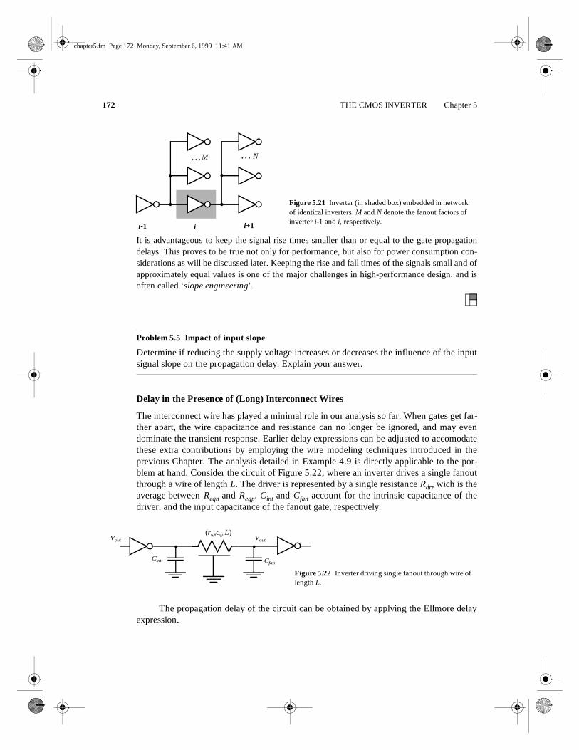
The interconnect wire has played a minimal role in our analysis so far. When gates get far-ther apart, the wire capacitance and resistance can no longer be ignored, and may evendominate the transient response. Earlier delay expressions can be adjusted to accomodatethese extra contributions by employing the wire modeling techniques introduced in theprevious Chapter. The analysis detailed in Example 4.9 is directly applicable to the por-blem at hand. Consider the circuit of Figure 5.22, where an inverter drives a single fanoutthrough a wire of length L. The driver is represented by a single resistance Rdr, wich is theaverage between Reqn and Reqp. Cint and Cfan account for the intrinsic capacitance of thedriver, and the input capacitance of the fanout gate, respectively.
The propagation delay of the circuit can be obtained by applying the Ellmore delayexpression.
……
i-1 i i+1
M N
Figure 5.21 Inverter (in shaded box) embedded in network of identical inverters. M and N denote the fanout factors of inverter i-1 and i, respectively.
Vout
(rw,cw,L)Vout
Cint Cfan
Figure 5.22 Inverter driving single fanout through wire of length L.
chapter5.fm Page 172 Monday, September 6, 1999 11:41 AM

Section 5.5 Power, Energy, and Energy-Delay 173
(5.32)
The 0.38 factor accounts for the fact that the wire represents a distributed delay. Cw andRw stand for the total capacitance and resistance of the wire, respectively. The delayexpressions contains a component that is linear with the wire length, as well a quadraticone. It is the latter that causes the wire delay to rapidly become the dominant factor in thedelay budget for longer wires.
Example 5.9 Inverter delay in presence of interconnect
Consider the circuit of Figure 5.22, and assume the device parameters of Example 5.5: Cint =3 fF, Cfan = 3 fF, and Rdr = 0.5(13/1.5 + 31/4.5) = 7.8 kΩ . The wire is implemented in metal1and has a width of 0.4 µm— the minimum allowed. This yields the following parameters: cw =92 aF/µm, and rw = 0.19 Ω/µm (Example 4.4). With the aid of Eq. (5.32), we can compute atwhat wire length the delay of the interconnect becomes equal to the intrinsic delay causedpurely by device parasitics. Solving the following quadratic equation yields a single usefulsolution.
Observe that the extra delay is solely due to the linear factor in the equation, and more specif-ically due to the extra capacitance introduced by the wire. The quadratic factor (this is, thedistributed wire delay) only becomes dominant at much larger wire lengths (> 7 cm). This isdue to the high resistance of the (minimum-size) driver transistors. A different balanceemerges when wider transistors are used. Analyze, for instance, the same problem with thedriver transistors 100 times wider, as is typical in high-speed, large fan-out drivers.
5.5 Power, Energy, and Energy-Delay
So far, we have seen that the static CMOS inverter with its almost ideal VTC— symmetri-cal shape, full logic swing, and high noise margins— offers a superior robustness, whichsimplifies the design process considerably and opens the door for design automation.Another major attractor for static CMOS is the almost complete absence of power con-sumption in steady-state operation mode. It is this combination of robustness and lowstatic power that has made static CMOS the technology of choice of most contemporarydigital designs. The power dissipation of a CMOS circuit is instead dominated by thedynamic dissipation resulting from charging and discharging capacitances.
tp 0.69RdrCint 0.69Rdr 0.38Rw+( )Cw 0.69 Rdr Rw+( )Cfan+ +=
0.69Rdr Cint Cfan+( ) 0.69 Rdrcw rwCfan+( )L 0.38rwcwL2+ +=
6.6 10 18–× L2 0.5 10 12– L×+ 32.29 10 12–×=or
L 65 µm=
chapter5.fm Page 173 Monday, September 6, 1999 11:41 AM

174 THE CMOS INVERTER Chapter 5
5.5.1 Dynamic Power Consumption
Dynamic Dissipation due to Charging and Discharging Capacitances
Each time the capacitor CL gets charged through the PMOS transistor, its voltage risesfrom 0 to VDD, and a certain amount of energy is drawn from the power supply. Part of thisenergy is dissipated in the PMOS device, while the remainder is stored on the load capac-itor. During the high-to-low transition, this capacitor is discharged, and the stored energyis dissipated in the NMOS transistor.3
A precise measure for this energy consump-tion can be derived. Let us first consider the low-to-high transition. We assume, initially, that the inputwaveform has zero rise and fall times, or, in otherwords, that the NMOS and PMOS devices are neveron simultaneously. Therefore, the equivalent circuitof Figure 5.23 is valid. The values of the energyEVDD, taken from the supply during the transition, aswell as the energy EC, stored on the capacitor at theend of the transition, can be derived by integratingthe instantaneous power over the period of interest.The corresponding waveforms of vout(t) and iVDD(t)are pictured in Figure 5.24.
(5.33)
(5.34)
These results can also be derived by observing that during the low-to-high transi-tion, CL is loaded with a charge CLVDD. Providing this charge requires an energy from thesupply equal to CLVDD
2 (= Q × VDD). The energy stored on the capacitor equals CLVDD2/2.
This means that only half of the energy supplied by the power source is stored on CL. Theother half has been dissipated by the PMOS transistor. Notice that this energy dissipationis independent of the size (and hence the resistance) of the PMOS device! During the dis-charge phase, the charge is removed from the capacitor, and its energy is dissipated in theNMOS device. Once again, there is no dependence on the size of the device. In summary,each switching cycle (consisting of an L→ H and an H→ L transition) takes a fixed amountof energy, equal to CLVDD
2. In order to compute the power consumption, we have to take
3 Observe that this model is a simplification of the actual circuit. In reality, the load capacitance consistsof multiple components some of which are located between the output node and GND, others between outputnode and VDD. The latter experience a charge-discharge cycle that is out of phase with the capacitances to GND,i.e. they get charged when Vout goes low and discharged when Vout rises. While this distributes the energy deliv-ery by the supply over the two phases, it does not impact the overall dissipation, and the results presented in thissection are still valid.
VDD
CL
vout
iVDD
Figure 5.23 Equivalent circuit during the low-to-high transition.
EVDD iVDD t( )VDD
0
∞
∫= dt VDD CLdvout
dt------------dt
0
∞
∫ CLVDD dvout
0
VDD
∫ CLVDD2= = =
EC iVDD t( )vout
0
∞
∫= dt CLdvout
dt------------ voutdt
0
∞
∫ CL voutdvout
0
VDD
∫ CLVDD2
2-----------------= = =
chapter5.fm Page 174 Monday, September 6, 1999 11:41 AM

Section 5.5 Power, Energy, and Energy-Delay 175
into account how often the device is switched. If the gate is switched on and off f0→ 1 timesper second, the power consumption equals
(5.35)
f0→ 1 represents the frequency of energy-consuming transitions, this is 0 → 1 transitionsfor static CMOS.
Advances in technology result in ever-higher of values of f0→ 1 (as tp decreases). Atthe same time, the total capacitance on the chip (CL) increases as more and more gates areplaced on a single die. Consider for instance a 0.25 µm CMOS chip with a clock rate of500 Mhz and an average load capacitance of 15 fF/gate, assuming a fanout of 4. Thepower consumption per gate for a 2.5 V supply then equals approximately 50 µW. For adesign with 1 million gates and assuming that a transition occurs at every clock edge, thiswould result in a power consumption of 50 W! This evaluation presents, fortunately, apessimistic perspective. In reality, not all gates in the complete IC switch at the full rate of500 Mhz. The actual activity in the circuit is substantially lower.
Example 5.10 Capacitive power dissipation of inverter
The capacitive dissipation of the CMOS inverter of Example 5.4 is now easily computed. InTable 5.2, the value of the load capacaitance was determined to equal 6 fF. For a supply volt-age of 2.5 V, the amount of energy needed to charge and discharge that capacitance equals
Assume that the inverter is switched at the maximum possible rate ( T = 1/f = tpLH +tpHL = 2 tp). For a tp of 32.5 psec (Example 5.5), we find that the dynamic power dissipation ofthe circuit is
Of course, an inverter in an actual circuit is rarely switched at this maximum rate, andeven if done so, the output does not swing from rail-to-rail. The power dissipation will hencebe substantially lower. For a rate of 4 GHz (T = 250 psec), the dissipation reduces to 150 µW.This is confirmed by simulations, which yield a power consumption of 155 µW.
t
t
v out
i VD
D
Charge Discharge Figure 5.24 Output voltages and supply current during (dis)charge of CL.
Pdyn CLVDD2 f0 1→=
Edyn CLVDD2 37.5 fJ= =
Pdyn Edyn 2tp( )⁄ 580 µW= =
chapter5.fm Page 175 Monday, September 6, 1999 11:41 AM

176 THE CMOS INVERTER Chapter 5
Computing the dissipation of a complex circuit is complicated by the f0→ 1 factor,also called the switching activity. While the switching activity is easily computed for aninverter, it turns out to be far more complex in the case of higher-order gates and circuits.One concern is that the switching activity of a network is a function of the nature and thestatistics of the input signals: If the input signals remain unchanged, no switching hap-pens, and the dynamic power consumption is zero! On the other hand, rapidly changingsignals provoke plenty of switching and hence dissipation. Other factors influencing theactivity are the overall network topology and the function to be implemented. We canaccomodate this by another rewrite of the equation, or
(5.36)
where f now presents the maximum possible event rate of the inputs (which is often theclock rate) and P0→ 1 the probability that a clock event results in a 0 → 1 (or power-con-suming) event at the output of the gate. CEFF = P0→ 1CL is called the effective capacitanceand represents the average capacitance switched every clock cycle. For our example, anactivity factor of 10% (P0→ 1 = 0.1) reduces the average consumption to 5 W.
Example 5.11 Switching activity
Consider the waveforms on theright where the upper waveformrepresents the idealized clock sig-nal , and the botttom one showsthe signal at the output of the gate.Power consuming transitionsoccur 2 out of 8 times, which isequaivalent to a transition proba-bility of 0.25 (or 25%).
With the increasing complexity of the digital integrated circuits, it is anticipated that the powerproblem will only worsen in future technologies. This is one of the reasons that lower supplyvoltages are becoming more and more attractive. Reducing VDD has a quadratic effect onPdyn. For instance, reducing VDD from 2.5 V to 1.25 V for our example drops the power dissipa-tion from 5 W to 1.25 W. This assumes that the same clock rate can be sustained. Figure 5.17demonstrates that this assumption is not that unrealistic as long as the supply voltage is sub-stantially higher than the threshold voltage. An important performance penalty occurs onceVDD approaches 2 VT.
When a lower bound on the supply voltage is set by external constraints (as often hap-pens in real-world designs), or when the performance degradation due to lowering the supplyvoltage is intolerable, the only means of reducing the dissipation is by lowering the effectivecapacitance. This can be achieved by addressing both of its components: the physical capaci-tance and the switching activity.
A reduction in the switching activity can only be accomplished at the logic and architec-tural abstraction levels, and will be discussed in more detail in later Chapters. Lowering the
Low Energy/Power Design Techniques
Pdyn CLVDD2 f0 1→ CLVDD
2 P0 1→ f CEFF VDD2 f= = =
Figure 5.25 Clock and signal waverforms
Clock
Output signal
chapter5.fm Page 176 Monday, September 6, 1999 11:41 AM

Section 5.5 Power, Energy, and Energy-Delay 177
physical capacitance is an overall worthwhile goal, which also helps to improve the perfor-mance of the circuit. As most of the capacitance in a combinational logic circuit is due to tran-sistor capacitances (gate and diffusion), it makes sense to keep those contributions to aminimum when designing for low power. This means that transistors should be kept to minimalsize whenever possible or reasonable. This definitely affects the performance of the circuit, butthe effect can be offset by using logic or architectural speed-up techniques. The only instanceswhere transistors should be sized up is when the load capacitance is dominated by extrinsiccapacitances (such as fan-out or wiring capacitance). This is contrary to common design prac-tices used in cell libraries, where transistors are generally made large to accommodate a rangeof loading and performance requirements.
The above observations lead to an interesting design challenge. Assume we have to min-imize the energy dissipation of a circuit with a specified lower-bound on the performance. Theobvious approach is to lower the supply voltage as much as possible, and to compensate theloss in performance by increasing the transistor sizes. Yet, the latter causes the capacitance toincrease. It may be foreseen that at a low enough supply voltage, the latter factor may start todominate and cause energy to increase with a further drop in the supply voltage.
To analyze the transistor-sizing for minimum energy problem, let us analyze the simplecase of a static CMOS inverter driving a load capacitance consisting of an intrinsic (Cint) andan extrinsic component (Cext) (Figure 5.26a). While the former represents the diffusion capaci-tances, the latter stands for wiring capacitance and fan-out. It is assumed that the ratio betweenPMOS and NMOS transistors is constant. The factor S stands for the inverter sizing factor,where S is equal to 1 for an inverter constructed of minimum-size devices. We can see that theintrinsic capacitance of the scaled device is proportional to S (or Cint(scaled) = SCint). Figure5.26b plots the normalized energy (per transition) as a function of the scaling factor S with theratio between the extrinsic and intrinsic capacitance as a parameter: α = Cext /Cint. The speed ofall implementations is kept constant by appropriately adjusting the supply voltage: larger val-ues of S normally mean lower values of the supply voltage.
1 1.5 2 2.5 3 3.5 4 4.5 50
1
2
3
4
5
Scaling Factor S
Norm
aliz
ed E
nerg
y
Figure 5.26 Normalized energy of a MOS inverter with load capacitance CL, as a function of the invertersize S and the ratio between the extrinsic and intrinsic capacitance α (= Cext/Cint). (assuming a referencesupply voltage of 2.5 V).
CL = Cext + SCint
S
(a) (b)
α=0
α=1α=2 α=5
chapter5.fm Page 177 Monday, September 6, 1999 11:41 AM

178 THE CMOS INVERTER Chapter 5
When α = 0 (or the load capacitance is zero), the lowest energy consumption is obtainedwhen using minimum-size devices. Only when the extrinsic capacitances dominate (α ≥ 1)does it make sense to widen the devices. This result should come as no surprise: transistor siz-ing to increase performance— and reduce the energy by lowering the supply voltage— onlymakes sense as long as performance is dominated by the extrinsic capacitance. Once the intrin-sic capacitance becomes the primary factor, further increases in the device sizes only raise theenergy consumption while no longer lowering the propagation delay. For example, a sizingfactor S of 3.75 minimizes the energy for a load of α = 5. The energy-reduction— with a factorof 4 with respect to the circuit instance with minimum-size devices— requires that the supplyvoltage be reduced to 1.03 V.
Example 5.12 Transistor Sizing for Inverter
We derive a simplified expression for the normalized energy of the inverter of Figure 5.26 asa function of S and α. The energy is normalized with respect to the case for S = 1, which iscalled the reference.
An expression for the propagation delay of the gate was already derived in Eq. (5.24),and is repeated here for convenience.
tpo stands for the intrinsic delay of the gate at the reference voltage VDD. Its dependence uponVDD is approximated by the following expression, derived from Eq. (5.21).
(5.37)
with VTE = VT + VDSAT/2 (assume a value averaged over NMOS and PMOS).Keeping the propagation delay of the scaled inverter constant with respect to the refer-
ence case means lowering the supply voltage:
where V′DD and VDD are the supply voltages of the scaled and reference inverters, respec-tively. The (normalized) dissipated energy of the scaled inverter is now derived:
The charts for VDD = 2.5 V and VTE = 0.75 V are plotted in Figure 5.26. Observe thatfor S >> α, the dissipation increases linearly with S. The reader should further be aware thatthe presented model is somewhat optimistic, as it ignores the extra energy dissipation relatedto the increased gate capacitance of the driving transistors.
tp 0.69 S α+( )C intReqn Reqp+
2S---------------------------
1 αS---+
tp0= =
tp0VDD
VDD VTE–-------------------------∼ 1
1 VTE VDD⁄–--------------------------------=
V′DD
VTE------------ S 1 α+( )
α S 1–( ) S α+( ) VTE VDD⁄( )+--------------------------------------------------------------------------=
E′Eref---------
S α+( )C int V′DD( )2
1 α+( )Cint VDD( )2--------------------------------------------- S α+( )S2 1 α+( )
α S 1–( ) VDD VTE⁄( ) S α+( )+( )2---------------------------------------------------------------------------------= =
chapter5.fm Page 178 Monday, September 6, 1999 11:41 AM
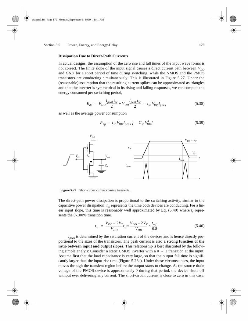
Section 5.5 Power, Energy, and Energy-Delay 179
Dissipation Due to Direct-Path Currents
In actual designs, the assumption of the zero rise and fall times of the input wave forms isnot correct. The finite slope of the input signal causes a direct current path between VDDand GND for a short period of time during switching, while the NMOS and the PMOStransistors are conducting simultaneously. This is illustrated in Figure 5.27. Under the(reasonable) assumption that the resulting current spikes can be approximated as trianglesand that the inverter is symmetrical in its rising and falling responses, we can compute theenergy consumed per switching period,
(5.38)
as well as the average power consumption
(5.39)
The direct-path power dissipation is proportional to the switching activity, similar to thecapacitive power dissipation. tsc represents the time both devices are conducting. For a lin-ear input slope, this time is reasonably well approximated by Eq. (5.40) where ts repre-sents the 0-100% transition time.
(5.40)
Ipeak is determined by the saturation current of the devices and is hence directly pro-portional to the sizes of the transistors. The peak current is also a strong function of theratio between input and output slopes. This relationship is best illustrated by the follow-ing simple analyis: Consider a static CMOS inverter with a 0 → 1 transition at the input.Assume first that the load capacitance is very large, so that the output fall time is signifi-cantly larger than the input rise time (Figure 5.28a). Under those circumstances, the inputmoves through the transient region before the output starts to change. As the source-drainvoltage of the PMOS device is approximately 0 during that period, the device shuts offwithout ever delivering any current. The short-circuit current is close to zero in this case.
Edp VDDIpeak tsc
2----------------- VDD
Ipeak tsc
2-----------------+ tsc VDDIpeak= =
Pdp tsc VDDIpeak f Csc VDD2 f= =
Figure 5.27 Short-circuit currents during transients.
VDD – VT
VT
Ipeak
t
t
vin
VDD
Vout
CL
Vin Isc
ishort
tscVDD 2VT–
VDD------------------------- ts
VDD 2VT–VDD
-------------------------tr f( )0.8--------×≈=
chapter5.fm Page 179 Monday, September 6, 1999 11:41 AM

180 THE CMOS INVERTER Chapter 5
Consider now the reverse case, where the output capacitance is very small, and the outputfall time is substantially smaller than the input rise time (Figure 5.28b). The drain-sourcevoltage of the PMOS device equals VDD for most of the transition period, guaranteeing themaximal short-circuit current (equal to the saturation current of the PMOS). This clearlyrepresents the worst-case condition. The conclusions of the above analysis are confirmedin Figure 5.29, which plots the short-circuit current through the NMOS transistor during alow-to-high transition as a function of the load capacitance.
This analysis leads to the conclusion that the short-circuit dissipation is minimizedby making the output rise/fall time larger than the input rise/fall time. On the other hand,making the output rise/fall time too large slows down the circuit and can cause short-cir-cuit currents in the fan-out gates. This presents a perfect example of how local optimiza-tion and forgetting the global picture can lead to an inferior solution.
A more practical rule, which optimizes the power consumption in a global way, can be formu-lated (Veendrick84]):
Design Techniques
Figure 5.28 Impact of load capacitance on short-circuit current.
VDD
Vout
CL
Vin
ISC ≈ 0
VDD
Vout
CL
Vin
ISC ≈ IMAX
(a) Large capacitive load (b) Small capacitive load
0 2 4 6
x 10-10
-0.5
0
0.5
1
1.5
2
2.5x 10
-4
time (sec)
I sc (A
)
Figure 5.29 CMOS inverter short-circuit current through NMOS transistor as a function of the load capacitance (for a fixed input slope of 500 psec).
CL = 20 fF
CL = 100 fF
CL = 500 fF
chapter5.fm Page 180 Monday, September 6, 1999 11:41 AM

Section 5.5 Power, Energy, and Energy-Delay 181
The power dissipation due to short-circuit currents is minimized by matching the rise/falltimes of the input and output signals. At the overall circuit level, this means that rise/falltimes of all signals should be kept constant within a range.
Making the input and output rise times of a gate identical is not the optimum solution forthat particular gate on its own, but keeps the overall short-circuit current within bounds. This isshown in Figure 5.30, which plots the short-circuit energy dissipation of an inverter (normal-
ized with respect to the zero-input rise time dissipation) as a function of the ratio r betweeninput and output rise/fall times. When the load capacitance is too small for a given inverter size(r > 2… 3 for VDD = 5 V), the power is dominated by the short-circuit current. For very largecapacitance values, all power dissipation is devoted to charging and discharging the loadcapacitance. When the rise/fall times of inputs and outputs are equalized, most power dissipa-tion is associated with the dynamic power and only a minor fraction (< 10%) is devoted toshort-circuit currents.
Observe also that the impact of short-circuit current is reduced when we lower thesupply voltage, as is apparent from Eq. (5.40). In the extreme case, when VDD < VTn + |VTp|,short-circuit dissipation is completely eliminated, because both devices are never onsimultaneously. With threshold voltages scaling at a slower rate than the supply voltage, short-circuit power dissipation is becoming of a lesser importance in deep-submicron technologies.At a supply voltage of 2.5 V and thresholds around 0.5 V, an input/output slope ratio of 2 isneeded to cause a 10% degradation in dissipation.
Finally, its is worth observing that the short-circuit power dissipation can be mod-eled by adding a load capacitance Csc = tscIpeak/VDD in parallel with CL, as is apparent inEq. (5.39). The value of this short-circuit capacitance is a function of VDD, the transistorsizes, and the input-output slope ratio.
0 1 2 3 4 50
1
2
3
4
5
6
7
8
tsin
/tsout
Pno
rm
Figure 5.30 Power dissipation of a static CMOS inverter as a function of the ratio between input and output rise/fall times. The power is normalized with respect to zero input rise-time dissipation. At low values of the slope ratio, input-output coupling leads to some extra dissipation.
W/L|P = 1.125 µm/0.25 µm
W/L|N = 0.375 µm/0.25 µmVDD = 3.3 V
VDD = 2.5 V
VDD = 1.5 V
CL = 30 fF
chapter5.fm Page 181 Monday, September 6, 1999 11:41 AM

182 THE CMOS INVERTER Chapter 5
5.5.2 Static Consumption
The static (or steady-state) power dissipation of a circuit is is expressed by Eq. (5.41),where Istat is the current that flows between the supply rails in the absence of switchingactivity
(5.41)
Ideally, the static current of the CMOS inverter is equal to zero, as the PMOS andNMOS devices are never on simultaneously in steady-state operation. There is, unfortu-nately, a leakage current flowing through the reverse-biased diode junctions of the transis-tors, located between the source or drain and the substrate as shown in Figure 5.31. Thiscontribution is, in general, very small and can be ignored. For the device sizes under con-sideration, the leakage current per unit drain area typically ranges between 10-100pA/µm2 at room temperature. For a die with 1 million gates, each with a drain area of 0.5µm2 and operated at a supply voltage of 2.5 V, the worst-case power consumption due todiode leakage equals 0.125 mW, which is clearly not much of an issue.
However, be aware that the junction leakage currents are caused by thermally gener-ated carriers. Their value increases with increasing junction temperature, and this occursin an exponential fashion. At 85°C (a common junction temperature limit for commercialhardware), the leakage currents increase by a factor of 60 over their room-temperature val-ues. Keeping the overall operation temperature of a circuit low is consequently a desirablegoal. As the temperature is a strong function of the dissipated heat and its removal mecha-nisms, this can only be accomplished by limiting the power dissipation of the circuitand/or by using chip packages that support efficient heat removal.
An emerging source of leakage current is the subthreshold current of the transistors.As discussed in Chapter 3, an MOS transistor can experience a drain-source current, evenwhen VGS is smaller than the threshold voltage (Figure 5.32). The closer the thresholdvoltage is to zero volts, the larger the leakage current at VGS = 0 V and the larger the staticpower consumption. To offset this effect, the threshold voltage of the device has generallybeen kept high enough. Standard processes feature VT values that are never smaller than0.5-0.6V and that in some cases are even substantially higher (~ 0.75V).
This approach is being challenged by the reduction in supply voltages that typicallygoes with deep-submicron technology scaling as became apparent in Figure 3.40. We con-
Pstat IstatVDD=
Vout = VDD
VDD
VDD
Drain LeakageCurrent
Subthreshold current Figure 5.31 Sources of leakage currents in CMOS inverter (for Vin = 0 V).
chapter5.fm Page 182 Monday, September 6, 1999 11:41 AM

Section 5.5 Power, Energy, and Energy-Delay 183
cluded earlier (Figure 5.17) that scaling the supply voltages while keeping the thresholdvoltage constant results in an important loss in performance, especially when VDDapproaches 2 VT . One approach to address this performance issue is to scale the devicethresholds down as well. This moves the curve of Figure 5.17 to the left, which means thatthe performance penalty for lowering the supply voltage is reduced. Unfortunately, thethreshold voltages are lower-bounded by the amount of allowable subthreshold leakagecurrent, as demonstrated in Figure 5.32. The choice of the threshold voltage hence repre-sents a trade-off between performance and static power dissipation. The continued scalingof the supply voltage predicted for the next generations of CMOS technologies will how-ever force the threshold voltages ever downwards, and will make subthreshold conductiona dominant source of power dissipation. Process technologies that contain devices with
sharper turn-off characteristic will therefore become more attractive. An example of thelatter is the SOI (Silicon-on-Insulator) technology whose MOS transistors have slope-fac-tors that are close to the ideal 60 mV/decade.
Example 5.13 Impact of threshold reduction on performance and static power dissipation
Consider a minimum size NMOS transistor in the 0.25 µm CMOS technology. In Chapter 3,we derived that the slope factor S for this device equals 90 mV/decade. The off-current (atVGS = 0) of the transistor for a VT of approximately 0.5V equals 10-11A (Figure 3.22). Reduc-ing the threshold with 200 mV to 0.3 V multiplies the off-current of the transistors with a fac-tor of 170! Assuming a million gate design with a supply voltage of 1.5 V, this translates intoa static power dissipation of 106 ×170×10-11×1.5 = 2.6 mW. A further reduction of the thresh-old to 100 mV results in an unacceptable dissipation of almost 0.5 W! At that supply voltage,the threshold reductions correspond to a performance improvement of 25% and 40%, respec-tively.
This lower bound on the thresholds is in some sense artificial. The idea that the leak-age current in a static CMOS circuit has to be zero is a preconception. Certainly, the pres-ence of leakage currents degrades the noise margins, because the logic levels are no longerequal to the supply rails. As long as the noise margins are within range, this is not a com-pelling issue. The leakage currents, of course, cause an increase in static power dissipa-
VT = 0.6VT = 0.2 VGS
Figure 5.32 Decreasing the threshold increases the subthreshold current at VGS = 0.
ID
chapter5.fm Page 183 Monday, September 6, 1999 11:41 AM

184 THE CMOS INVERTER Chapter 5
tion. This is offset by the drop in supply voltage, that is enabled by the reduced thresholdsat no cost in performance, and results in a quadratic reduction in dynamic power. For a0.25 µm CMOS process, the following circuit configurations obtain the same perfor-mance: 3 V supply–0.7 V VT; and 0.45 V supply–0.1 V VT. The dynamic power consump-tion of the latter is, however, 45 times smaller [Liu93]! Choosing the correct values ofsupply and threshold voltages once again requires a trade-off. The optimal operation pointdepends upon the activity of the circuit. In the presence of a sizable static power dissipa-tion, it is essential that non-active modules are powered down, lest static power dissipationwould become dominant. Power-down (also called standby) can be accomplished by dis-connecting the unit from the supply rails, or by lowering the supply voltage.
5.5.3 Putting It All Together
The total power consumption of the CMOS inverter is now expressed as the sum of itsthree components:
(5.42)
In typical CMOS circuits, the capacitive dissipation is by far the dominant factor. Thedirect-path consumption can be kept within bounds by careful design, and should hencenot be an issue. Leakage is ignorable at present, but this might change in the not too dis-tant future.
The Power-Delay Product, or Energy per Operation
In Chapter 1, we introduced the power-delay product (PDP) as a quality measure for alogic gate.
(5.43)
The PDP presents a measure of energy, as is apparent from the units (Wsec = Joule).Assuming that the gate is switched at its maximum possible rate of fmax = 1/(2tp), andignoring the contributions of the static and direct-path currents to the power consumption,we find
(5.44)
The PDP stands for the average energy consumed per switching event (this is, for a0→ 1, or a 1→ 0 transition). Remember that earlier we had defined Eav as the averageenergy per switching cycle (or per energy-consuming event). As each inverter cycle con-tains a 0→ 1, and a 1→ 0 transition, Eav hence is twice the PDP.
Energy-Delay Product
The validity of the PDP as a quality metric for a process technology or gate topology isquestionable. It measures the energy needed to switch the gate, which is an important
P tot Pdyn Pdp P+ + stat CLVDD2 VDDIpeak ts+( )f0 1→ VDDIleak+= =
PDP Pavtp=
PDP CLVDD2 fmax tp
CLVDD2
2-----------------= =
chapter5.fm Page 184 Monday, September 6, 1999 11:41 AM

Section 5.5 Power, Energy, and Energy-Delay 185
property for sure. Yet for a given structure, this number can be made arbitrarily low byreducing the supply voltage. From this perspective, the optimum voltage to run the circuitat would be the lowest possible value that still ensures functionality. This comes at themajor expense in performance, at discussed earlier. A more relevant metric should com-bine a measure of performance and energy. The energy-delay product (EDP) does exactlythat.
(5.45)
It is worth analyzing the voltage dependence of the EDP. Higher supply voltages reducedelay, but harm the energy, and the opposite is true for low voltages. An optimum opera-tion point should hence exist. Assuming that NMOS and PMOS transistors have compari-ble threshold and saturation voltages, we can simplify the propagation delay expressionEq. (5.21).
(5.46)
where VTe = VT + VDSAT/2, and α technology parameter. Combining Eq. (5.45) and Eq.(5.46), 4
(5.47)
The optimum supply voltage can be obtained by taking the derivative of Eq. (5.47) withrespect to VDD, and equating the result to 0.
(5.48)
The remarkable outcome from this analysis is the low value of the supply voltagethat simultaneously optimizes performance and energy. For sub-micron technologies withthresholds in the range of 0.5 V, the optimum supply is situated around 1 V.
Example 5.14 Optimum supply voltage for 0.25 µm CMOS inverter
From the technology parameters for our generic CMOS process presented in Chapter 3, thevalue of VTE can be derived.
VTn = 0.43 V, VDsatn = 0.63 V, VTEn = 0.74 V.VTp = -0.4 V, VDsatp = -1 V, VTEp = -0.9 V.
VTE ≈ (VTEn+|VTEp|)/2 = 0.8 V
Hence, VDDopt = (3/2) × 0.8 V = 1.2 V. The simulated graphs of Figure 5.33, plotting normal-ized delay, energy, and energy-delay product, confirm this result. The optimum supply volt-
4 This equation is only accurate as long as the devices remain in velocity saturation, which is probablynot the case for the lower supply voltages. This introduces some inaccurarcy in the analysis, but will not distortthe overall result.
EDP PDP tp× P= avtp2 CLVDD
2
2----------------- tp= =
tpαCLVDD
VDD VTe–------------------------≈
EDPαCL
2VDD3
2 VDD VTE–( )---------------------------------=
VDDopt32---VTE=
chapter5.fm Page 185 Monday, September 6, 1999 11:41 AM

186 THE CMOS INVERTER Chapter 5
age is predicted to equal 1.1 V. The charts clearly illustrate the trade-off between delay andenergy.
WARNING: While the above example demonstrates that there exists a supply voltagethat minimizes the energy-delay product of a gate, this voltage does not necessarily repre-sent the optimum voltage for a given design problem. For instance, some designs require aminimum performance, which requires a higher voltage at the expense of energy. Simi-larly, a lower-energy design is possible by operating by circuit at a lower voltage and byobtaining the overall system performance through the use of architectural techniques suchas pipelining or concurrency.
5.5.4 Analyzing Power Consumption Using SPICE
A definition of the average power consumption of a circuit was provided in Chapter 1, andis repeated here for the sake of convenience.
(5.49)
with T the period of interest, and VDD and iDD the supply voltage and current, respectively.Some implementations of SPICE provide built-in functions to measure the average valueof a circuit signal. For instance, the HSPICE .MEASURE TRAN I(VDD) AVG commandcomputes the area under a computed transient response (I(VDD)) and divides it by theperiod of interest. This is identical to the definition given in Eq. (5.49). Other implementa-tions of SPICE are, unfortunately, not as extensive. This is not as bad as it seems, as longas one realizes that SPICE is actually a differential equation solver. A small circuit caneasily be conceived that acts as an integrator and whose output signal is nothing but theaverage power.
0.5 1 1.5 2 2.50
5
10
15
VDD
(V)
Ener
gy-D
elay
(nor
m)
Figure 5.33 Normalized delay, energy, and energy-delay plots for CMOS inverter in 0.25 µm CMOS technology.
EnergyDelay
Energy-Delay
Pav1T--- p t( )dt
0
T
∫ VDD
T---------- iDD t( )dt
0
T
∫= =
chapter5.fm Page 186 Monday, September 6, 1999 11:41 AM

Section 5.5 Power, Energy, and Energy-Delay 187
Consider, for instance, the circuit of Figure 5.34. The current delivered by the powersupply is measured by the current-controlled current source and integrated on the capaci-tor C. The resistance R is only provided for DC-convergence reasons and should be cho-sen as high as possible to minimize leakage. A clever choice of the element parameterensures that the output voltage Pav equals the average power consumption. The operationof the circuit is summarized in Eq. (5.50) under the assumption that the initial voltage onthe capacitor C is zero.
(5.50)
Equating Eq. (5.49) and Eq. (5.50) yields the necessary conditions for the equivalentcircuit parameters: k/C = VDD/T. Under these circumstances, the equivalent circuit shownpresents a convenient means of tracking the average power in a digital circuit.
Example 5.15 Average Power of Inverter
The average power consumption of the inverter of Example 5.4 is analyzed using the abovetechnique for a toggle period of 250 psec (T = 250 psec, k = 1, VDD = 2.5 V, hence C = 100pF). The resulting power consumption is plotted in Figure 5.35, showing an average powerconsumption of approximately 157.3 µW. The .MEAS AVG command yields a value of160.32 µW, which demonstrates the approximate equivalence of both methods. These num-beres are equivalent to an energy of 39 fJ (which is close to the 37.5 fJ derived in Example5.10). Observe the slightly negative dip during the high-to-low transition. This is due to theinjection of current into the supply, when the output briefly overshoots VDD as a result of thecapacitive coupling between input and output (as is apparent from in the transient response ofFigure 5.16).
Ctd
dPav kiDD=
or
PavkC---- iDDdt
0
T
∫=
Figure 5.34 Equivalent circuit to measure average power in SPICE.
RC
k iDDCircuit
under test
+
–
VDD
iDD
Pav
chapter5.fm Page 187 Monday, September 6, 1999 11:41 AM

188 THE CMOS INVERTER Chapter 5
5.6 Perspective: Technology Scaling and its Impact on the Inverter Metrics
In section 3.5, we have explored the impact of the scaling of technology on the some ofthe important design parameters such as area, delay, and power. For the sake of clarity, werepeat here some of the most important entries in the resulting scaling table (Table 3.8).
Table 5.3 Scaling scenarios for short-channel devices (S and U represent the technology and voltage scaling parameters, respectively).
Parameter Relation Full Scaling General Scaling Fixed-Voltage Scaling
Area/Device WL 1/S2 1/S2 1/S2
Intrinsic Delay RonCgate 1/S 1/S 1/S
Intrinsic Energy CgateV2 1/S3 1/SU2 1/S
Intrinsic Power Energy/Delay 1/S2 1/U2 1
Power Density P/Area 1 S2/U2 S2
0 0.5 1 1.5 2 2.5
x 10-10
0
0.2
0.4
0.6
0.8
1
1.2
1.4
1.6
1.8x 10
-4
t (sec)
powe
r (W
)
Figure 5.35 Deriving the power consumption using SPICE.
Average Power
Vin: 0→ 1
(over one cycle)
chapter5.fm Page 188 Monday, September 6, 1999 11:41 AM

Section 5.6 Perspective: Technology Scaling and its Impact on the Inverter Metrics 189
To validity of these theoretical projections canbe verified by looking back and observing thetrends during the past decades. From , we canderive that the gate delay indeed decreasesexponentially at a rate of 13%/year, or halvingevery five years. This rate is on course withthe prediction of Table 5.3, since S averagesapproximately 1.15 as we had alreadyobserved in Figure 3.39. The delay of a 2-input NAND gate with a fanout of four hasgone from tens of nanoseconds in the 1960s toa tenth of a nanosecond in the year 2000, andis projected to be a few tens of picoseconds by2010.
Reducing power dissipation has only been a second-order priority until recently.Hence, statistics on dissipation-per-gate or design are only marginally available. An inter-esting chart is shown in Figure 5.37, which plots the power density measured over a largenumber of designs produced between 1980 and 1995. Although the variation islarge— even for a fixed technology— it shows the power density to increase approximatelywith S2. This is in correspondence with the fixed-voltage scaling scenario presented inTable 5.3. For more recent years, we expect a scenario more in line with the the full-scal-ing model— which predicts a constant power density— due to the accelerated supply-volt-age scaling and the increased attention to power-reducing design techniques. Even underthese circumstances, power dissipation-per-chip will continue to increase due to the ever-larger die sizes.
The presented scaling model has one fatal flaw however: the performance andpower predictions produce purely “intrinsic” numbers that take only device parametersinto account. In Chapter 4, it was concluded that the interconnect wires exhibit a differentscaling behavior, and that wire parasitics may come to dominate the overall performance.Similarly, charging and discharging the wire capacitances may dominate the energy bud-
Figure 5.36 Scaling of the gate delay (from [Dally98]).
Figure 5.37 Evolution of power-density in micro- and DSP processors, as a function of the scaling factor S ([Sakurai]). S is normalized to 1 for a 4 µm process.
∝ S2
S
chapter5.fm Page 189 Monday, September 6, 1999 11:41 AM

190 THE CMOS INVERTER Chapter 5
get. To get a crisper perspective, one has to construct a combined model that considersdevice and wire scaling models simultaneously. The impact of the wire capacitance and itsscaling behavior is summarized in Table 5.4. We adopt the fixed-resistance model intro-duced in Chapter 4. We furthermore assume that the resistance of the driver dominates thewire resistance, which is definitely the case for short to medium-long wires.
The model predicts that the interconnect-caused delay (and energy) gain in impor-tance with the scaling of technology. This impact is limited to an increase with εc for shortwires (S = SL), but it becomes increasingly more outspoken for medium-range and longwires (SL < S). These conclusions have been confirmed by a number of studies, an exam-ple of which is shown in Figure 5.38. How the ratio of wire over intrinsic contributions
will actually evolve is debatable, as it depends upon a wide range of independent parame-ters such as system architecture, design methodology, transistor sizing, and interconnectmaterials. The doomday scenario that interconnect may cause CMOS performance to sat-urate in the very near future hence may be exagerated. Yet, it is clear to that increasedattention to interconnect is an absolute necessity, and may change the way the next-gener-ation circuits are designed and optimized (e.g. Sylvester99]).
Table 5.4 Scaling scenarios for wire capacitance. S and U represent the technology and voltage scaling parameters, respectively, while SL stands for the wire-length scaling factor. εc represents the impact of fringing and interwire capacitances.
Parameter Relation General Scaling
Wire Capacitance WL/t εc/SL
Wire Delay RonCint εc/SL
Wire Energy CintV2 εc/SLU2
Wire Delay / Intrinsic Delay εcS/SL
Wire Energy / Intrinsic Energy εcS/SL
Figure 5.38 Evolution of wire delay / gate delay ratio with respect to technology (from [Fisher98]).
chapter5.fm Page 190 Monday, September 6, 1999 11:41 AM

Section 5.7 Summary 191
5.7 Summary
This chapter presented a rigourous and in-depth analysis of the static CMOS inverter. Thekey characteristics of the gate are summarized:
• The static CMOS inverter combines a pull-up PMOS section with a pull-downNMOS device. The PMOS is normally made wider than the NMOS due to its infe-rior current-driving capabilities.
• The gate has an almost ideal voltage-transfer characteristic. The logic swing is equalto the supply voltage and is not a function of the transistor sizes. The noise marginsof a symmetrical inverter (where PMOS and NMOS transistor have equal current-driving strength) approach VDD/2. The steady-state response is not affected by fan-out.
• Its propagation delay is dominated by the time it takes to charge or discharge theload capacitor CL. To a first order, it can be approximated as
Keeping the load capacitance small is the most effective means of implementinghigh-performance circuits. Transistor sizing may help to improve performance aslong as the delay is dominated by the extrinsic (or load) capacitance of fanout andwiring.
• The power dissipation is dominated by the dynamic power consumed in chargingand discharging the load capacitor. It is given by P0→ 1 CLVDD
2f. The dissipation isproportional to the activity in the network. The dissipation due to the direct-pathcurrents occuring during switching can be limited by careful tailoring of the signalslopes. The static dissipation can usually be ignored but might become a major fac-tor in the future as a result of subthreshold currents.
• Scaling the technology is an effective means of reducing the area, propagation delayand power consumption of a gate. The impact is even more striking if the supplyvoltage is scaled simultaneously.
• The interconnect component is gradually taking a larger fraction of the delay andperformance budget.
5.8 To Probe Further
The operation of the CMOS inverter has been the topic of numerous publications and text-books. Virtually every book on digital design devotes a substantial number of pages to theanalysis of the basic inverter gate. An extensive list of references was presented in Chapter1. Some references of particular interest that were explicitly quoted in this chapter aregiven below.
tp 0.69CLReqn Reqp+
2---------------------------
=
chapter5.fm Page 191 Monday, September 6, 1999 11:41 AM

192 THE CMOS INVERTER Chapter 5
REFERENCES
[Baccarani84] G. Baccarani, M. Wordeman, and R. Dennard, “Generalized Scaling Theory and ItsApplication to 1/4 Micrometer MOSFET Design,” IEEE Trans. Electron Devices, ED-31(4):p. 452, 1984.
[Brews89] J. Brews et al., “The Submicrometer Silicon MOSFET,” in [Watts89].[De Man87] De Man H., Computer Aided Design of Digital Integrated Circuits, Lecture Notes,
Katholieke Universiteit Leuven, Belgium.[Dennard74] R. Dennard et al., “Design of Ion-Implanted MOSFETS with Very Small Physical
Dimensions,” IEEE Journal of Solid-State Circuits, SC-9, pp. 256–258, 1974.[Embabi93] S. Embabi, A. Bellaouar, M. Elmasry, Digital BiCMOS Integrated Circuit Design,
Kluwer Academic Publishers, 1993.[Hodges88] D. Hodges and H. Jackson, Analysis and Design of Digital Integrated Circuits,
McGraw-Hill, 1988.[Jouppi93] N. Jouppi et al., “A 300 MHz 115W 32b Bipolar ECL Microprocessor with On-Chip
Caches,” Proc. IEEE ISSCC Conf., pp. 84–85, February 1993.[Kakumu90] M. Kakumu and M. Kinugawa, “Power-Supply Voltage Impact on Circuit Perfor-
mance for Half and Lower Submicrometer CMOS LSI,” IEEE Journal of Solid-State Circuits,vol. 37, no. 8, pp. 1900–1908, August 1990.
[Lohstroh81] J. Lohstroh, “Devices and Circuits for Bipolar (V)LSI,” Proceedings of the IEEE, vol.69, pp. 812–826, July 1981.
[Masaki92] A. Masaki, “Deep-Submicron CMOS Warms Up to High-Speed Logic,” IEEE Circuitsand Devices Magazine, pp. 18–24, November 1992.
[Schutz94] J. Schutz, “A 3.3V 0.6 mm BiCMOS Superscaler Microprocessor,” ISSCC Digest ofTechnical Papers, pp. 202–203, February 1994.
[Sedra87] Sedra and Smith, MicroElectronic Circuits, Holt, Rinehart and Winston, 1987.[Shoji88] Shoji, M., CMOS Digital Circuit Technology, Prentice Hall, 1988.[Tang89] D. Tang, “Scaling the Silicon Bipolar Transistor,” in [Watts89].[Veendrick84] H. Veendrick, “Short-Circuit Dissipation of Static CMOS Circuitry and its Impact on
the Design of Buffer Circuits,” IEEE Journal of Solid-State Circuits, vol. SC-19, no. 4,pp. 468–473, 1984.
[Watts89] Watts R., ed., SubMicron Integrated Circuits, Wiley, 1989.
5.9 Exercises and Design Problems
For all problems, use the device parameters provided in Chapter 3 (as well as the inside back cover),unless otherwise mentioned.
1. [M, SPICE, 3.3.2] The layout of a static CMOS inverter is given in Figure 5.39. (1λ = 0.6µm).a. Determine the sizes of the NMOS and PMOS transistor.b. Derive the VTC and its parameters (VOH, VOL, VM, VIH, and VIL).c. Is the VTC affected when the output of the gates is connected to the inputs of 4 similar
gates?
chapter5.fm Page 192 Monday, September 6, 1999 11:41 AM


![Chapter5 New (Cementing)[1]](https://img.dokumen.tips/doc/110x75/577d1cf41a28ab4e1e8b47f6/chapter5-new-cementing1.jpg)


![Chapter5[1]-Effects of physical barrier](https://img.dokumen.tips/doc/110x75/577dabe41a28ab223f8d1d32/chapter51-effects-of-physical-barrier.jpg)

![RS InstructorPPT Chapter5[1]](https://img.dokumen.tips/doc/110x75/55cf8e5a550346703b91416d/rs-instructorppt-chapter51.jpg)