Embed Size (px)
Citation preview
© 2015 BrPhotonics Confidential All Rights Reserved
High Speed Integrated Photonics DevicesOptical Transmission at 100G and Beyond
Júlio César R.F. de Oliveira, Ph.D., CEOMay, 2015

2 © 2015 BrPhotonics Confidential All Rights Reserved
Outline BrPhotonics Optical Transciever Market Strategy
- Photonics & Microelectronics Convergence/Verticalization Integrated Devices Technologies
– Polymer Modulators (Foundry Based)– Silicon Photonics (Passive and Active Devices)
Advanced Optical Packaging Capabilities Integrated Optical Transcievers
– 100/200G TOSA/CFP2 and u-Thin Modulator Microelectronics
– IPs and ASICs Tunable LASER ROADMAP Final Comments

3 © 2015 BrPhotonics Confidential All Rights Reserved
BrPhotonicsBrPhotonics (BrP) is a provider of advanced high-speed devices for optical communications and integrated transceiver components that enable information streaming over communication networks. The products utilize technologies such as Silicon Photonics (SiPh) and Thin Films Polymer on Silicon (TFPSTM) to advance the 100Gbps to 1Tbps fiber-optics long haul and metro links. Microelectronic (ASICs) for photonics aplications is another driver for BrP. BrPhotonics portfolio of small form factor components addresses CFP2 and CFP4 applications by enabling a greater network capacity through superior linearization, multi-level modulation, and other advanced techniques.
GigOptix• Polymer foundry in TFPS (transfer from Seattle to Campinas)• Strong expertize in high speed analog (TIA and Drivers)• World wide operations, sales and marketing• Well stablished with potential BRPhotonics customers
CPqD• Strong photonic design and packging technology • World class system know-how• Established R&D program on Photonics and Microelectronics • Connections with industry leaders driving technology transfer
BrPhotonics IP : total of 24 patents- 17 patents on TFPS Technology- 4 patents applications on Silicon Photonics Technology- 3 patents applications on DSP design
Technology: TFPS, Silicon Photonics, SFF Packaging and Microelectronics

4 © 2015 BrPhotonics Confidential All Rights Reserved
BrPhotonics – (%)
March’14 to Dez’14 Jan’15 to June’15 Aug’15 ...*
*Negotiations closed, under Due Diligence

5 © 2015 BrPhotonics Confidential All Rights Reserved
BrPhotonics Location and FacilitiesCPqD Campus, Campinas, Brazil
Production Facility
• for Thin Film Polymer on Silicon (TFPS) Modulators and Packaging
Cleanrooms• Class 100• Class 10000
Labs• Optical Transmission• Packaging• Qualification

6 © 2015 BrPhotonics Confidential All Rights Reserved
High Speed Optical Transciever Market100G TAM = Submounts -TOSA/ROSA + Components USD1.746B @2015 and USD 3.9715B @2019
100G Componnents = USD1.15B @2015 and USD 4.9B @2019
100G Datacom USD 0.79B@2015/USD 3.5B@2019 ; Telecom USD 0.516B@2015/USD1.41B@2019

7 © 2015 BrPhotonics Confidential All Rights Reserved
Long Haul/Metro Transceiver Market Dynamics
SFF, Integration, Low Power Consumption, Low Cost
100Gbps
1Tbps 400Gbps
200Gbps
100G
b/s
200G
b/s
400G
b/s
1Tb/
s
Line
Rat
e Ev
oluti
on
Form Factor Reduction
MSA CFP CFP2 CFP4 QSFP

8 © 2015 BrPhotonics Confidential All Rights Reserved
Coherent LineCard... Density +++++1x100G MSA 5x7
2x100G CFP
5x100G CFP2
2012
2014
2016
12,7 cm10,16 cm
8,2 cm 4,1 cm 2,4 cm

9 © 2015 BrPhotonics Confidential All Rights Reserved
Optical Communications needs Integration Photonic Integration divers
– Data traffic increase– Lack of bandwidth to support in electrical
domain
Solutions– Integrated Photonics– Microelectronics
Main Devices (Long Haul)– Modulators and Photodetectors– Transcievers (Transmissores/Receptores)– Tunable lasers– ASICs to photonics (DSP, OTN, Monitoring,...)
Enabling Technologies– Polymer, InP, Silicon– Packaging (Hybrid and Monolitic)– Digital Signal Processing– Transport switching
Photonic IC Design Photonic Packaging High Speed Analog Microelectronic

10 © 2015 BrPhotonics Confidential All Rights Reserved
Photonics and Microelectronics - Convergence
Integrated Photonics– Silicon Photonics
» Passives for 1550/1310» Actives (Mod., Rec., ...)» Today: Metro/Access» Future: + Long Haul
– TFPS– InP– Hybrid Integration
» Si-TFPS» II-V/Si
Microlectronics– IPs– ASICs– High Speed Analog
» TIA» Drivers
– Packaging » Wirebonded» Interposer» Flip-chip» Monolithic

11 © 2015 BrPhotonics Confidential All Rights Reserved
BrPhotonics ... Market Chain Value
Discrete components
Submount (TOSA/ROSA)
Telecom
Others MKT

12 © 2015 BrPhotonics Confidential All Rights Reserved
TX
RX
LINE
TX
RX
CLIENT
Current global scenarioCritical componentes ≥ 100Gbps
Digital Microelectronics (<40nm)
Integrated Photonics
High Speed Analog

13 © 2015 BrPhotonics Confidential All Rights Reserved
BrPhotonics ... Verticalizing
TX
RX
LINE
TX
RX
CLIENT
Digital Microelectronics (<40nm)
Integrated Photonics
High Speed Analog
OTN
Tunable Laser
DSP
Driver28G
TIA28G
Modulator
Receiver

14 © 2015 BrPhotonics Confidential All Rights Reserved
Photonics and Microelectronics - Convergence
Photonics
Microelectronics
Wirebonder Flip-ChipInterposer
Monolithic90nm?
15 © 2015 BrPhotonics Confidential All Rights Reserved
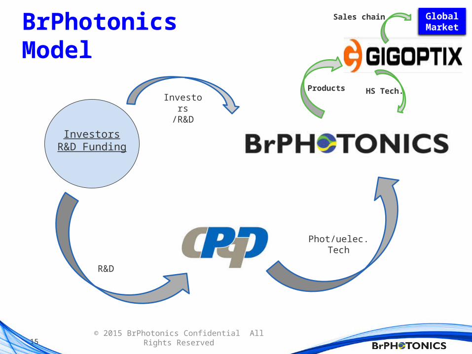
BrPhotonics Model
InvestorsR&D Funding
R&D
Phot/uelec. Tech
#1
Global Market
Sales chain
HS Tech.ProductsInvestors
/R&D

16 © 2015 BrPhotonics Confidential All Rights Reserved
Integrated Photonics Devices Technologies- Polymer Modulators- Silicon Photonics

17 © 2015 BrPhotonics Confidential All Rights Reserved
Electro-Optic (EO) Polymers
• Electrical field changes refractive index of material• Polarization happens in femtoseconds• Max operation frequency is dependent on RF loss of the electrode
• Composite formed with a chromophore and a polymer – similar with semiconductor doping
• Polarization of chromophore responsible for EO effect
electricfield
acceptor
donor
+
-
Host polymer
Guest polymer(Chromophore)

18 © 2015 BrPhotonics Confidential All Rights Reserved
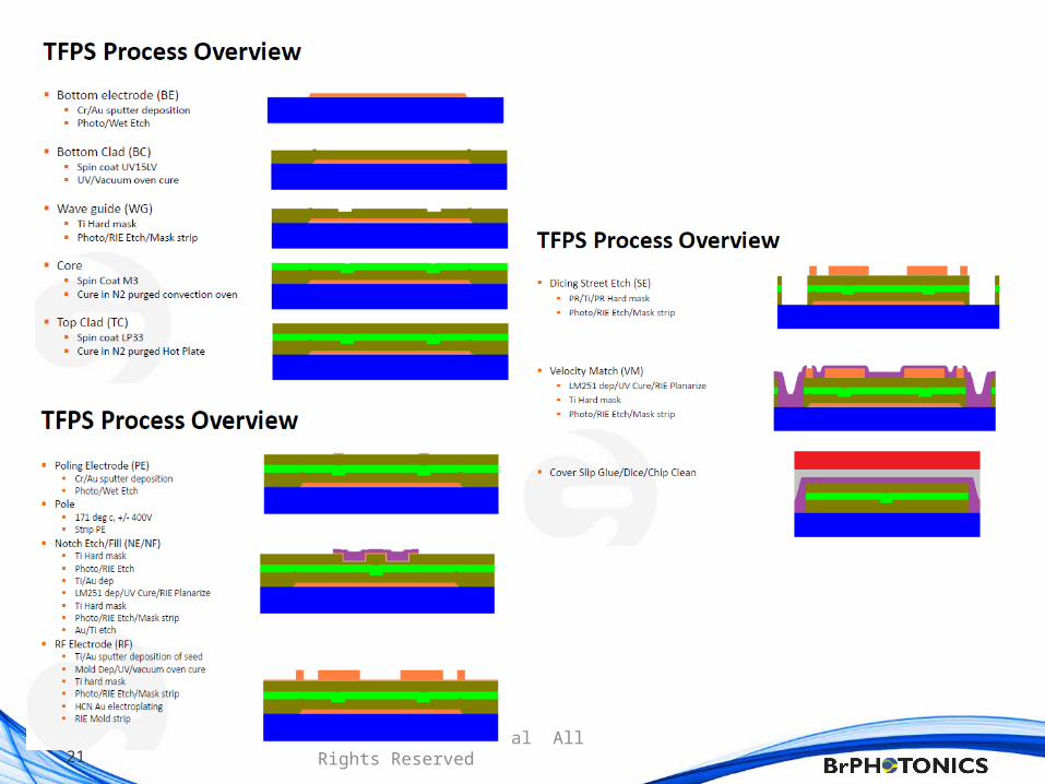
Manufacturing of TFPS Modulators Chips
Top clad
Electro-optic polymer
End of waveguideWaveguide trench
Bottom clad
Ground plane
Silicon substrate
Top electrode
Ground pads
• BrPhotonics has a 200m2, class 10 cleanroom in Seattle (In transfer to Campinas)
• Team of chemists, process, RF, and optical engineers
• Specialized in the manufacture of EO polymer modulators
• Capacity of 200 wafers/year

19 © 2015 BrPhotonics Confidential All Rights Reserved
LP33Synth
GV101Cert
WaferBottom
ElectrodeBottomClad
WaveGuide
CORETopClad
Poling NotchStreetEtch
RFElectrode
VelocityMatch
DICE Via Test
APCCert
PVPCert
LM251Synth
LM251Cert
APCPurific
PVPFormul
LP33Cert
LM251Synth
LM251Cert
LP156Cert
LP156Formul
GS2Synth
GS2Cert
CoreMonitor
CoreFormul
Donor Synth
Bridge Synth
Donor Charac
Bridge Charac
Donor/Bridge Synth
Donor/Bridge Cert
UV15MB
UV15Cert
GS2 Synth
GS2Cert
Acceptor Synth
AP5Synth
AP5Cert
B74 Purific
B74Cert
Wafer Process Flow
Material F
low
Synthesis
Characterization
Certification
Formulation
Commertial
APC
Acceptor Charac
Material Synthesis
Chemicals
Certification
Chemicals
Certification

20 © 2015 BrPhotonics Confidential All Rights Reserved
Wafer Process Flow
Wafer Start
Bottom Electrode
Bottom Clad
Wave Guide
Core Top Clad
PolingRF
ElectrodeNotch
Street Etch
Velocity Match
Dice Via Test
SC1 Clean
Cr/Au Sputter
Photo
Wet Etch
Ti Sputter Hardmask
Photo
Plasma Etch
Strip Strip
UV15 Coat
UV Cure
Thermal Cure
B74 Coat
Thermal Cure
Etch Back
LP33 Coat
Thermal Cure
Etch Back
Cr/Au Sputter
Photo
Wet Etch
Strip
Disconnect
PVP
Pole
Strip
Ti/Au Sputter
LP156 Coat
UV Cure
Ti Sputter Hardmask
Photo
Plasma Etch
Strip
Plate
Photo
Plasma Etch
Ti/Au Coat
Strip
LM251 Coat
Etch Back
Etch Back
Ti Sputter Hardmask
Photo
Plasma Etch
Wet Etch
Ti Sputter Hardmask
Photo
Plasma Etch
Strip
Ti Sputter Hardmask
Photo
Plasma Etch
Strip
LM251 Coat
UV+Therm Cure
Etch Back
UV+Therm Cure
Coverslip Attach
Thermal Cure
Photo
Photo
Plasma Etch
Thermal Cure
Photolitography
UV/Thermal Cure
Metal Sputter
Coating
Plasma Etch
Wet Etch
Strip
Wafer Process Flow
Pro
cess Flo
w
21 © 2015 BrPhotonics Confidential All Rights Reserved

22 © 2015 BrPhotonics Confidential All Rights Reserved
TFPS Wafer Process Foundry
300 m2 clean room (Class 100 & 10K)EO Polymer Synthesis
Full 6” wafer fab capabilityAdvanced Dye test Capability (DC&RF)

23 © 2015 BrPhotonics Confidential All Rights Reserved
Advanced Packaging Capability
Active Alingment Sealing and Wire Bonder
Laser Welding
Dye Bonder/ Flip Chip

24 © 2015 BrPhotonics Confidential All Rights Reserved
100G/200G CFP2 TOSA 100G/200G U-Thin Modulator

25 © 2015 BrPhotonics Confidential All Rights Reserved
Product application
Line-side optical transport Product main applications
– CFP2 form factor Analog Coherent Optics (ACO) modules
– OIF modules and line cards Higher integration and cost reduction
– Metro and long-haul applications High-speed line rate
– Symbol rate agnostic (up to 32 GBd) 100 Gb/s DP-QPSK 200 Gb/s DP-16QAM
Advanced modulation– Polarization-multiplexing– Digital modulation formats– Advanced pulse-shaping
CFP2 Mechanical Module
Example: TOSA in CFP2 module

26 © 2015 BrPhotonics Confidential All Rights Reserved
Product features
Features– Small form-factor– Innovative solderless LGA Package– 3 hermetic optical windows allowing TX and
LO exit fiber to be available at the same or opposite side for enhanced layout placement inside CFP2 modules.
Modulator features– Low optical insertion loss– 85oC temperature operation– Zero chirp– Low driving voltage
Tunable laser features– High output power– Full C-band tunability– ITU-T DWDM grid– Narrow linewidth
Photonic integration– Thin-Film Polymer on Silicon (TFPS)
Modulator– Tunable laser– Polarization-Multiplexing Free-Space
Optics (PolMux FSO)
TXLO2
LO1

27 © 2015 BrPhotonics Confidential All Rights Reserved
TOSA package RF performance simulation
0 5 10 15 20 25 30 35 40 45 50-30
-25
-20
-15
-10
-5
0
Frequency (GHz)
S21
[so
lid]
/ S
11 [
dash
ed]
(dB
)
Port 1,2
Port 3,4
Port 5,6
Port 7,8
-14 dB
-3 dBPort S21* S11**
1,2 36 GHz
-17 dB
3,4 36 GHz
-14 dB
5,6 36 GHz
-14 dB
7,8 36 GHz
-18 dB
Main Parameters
*S21 bandwidth at -3 dB.**S11 from 0 up to 30 GHz.
S Curves – Package ports

28 © 2015 BrPhotonics Confidential All Rights Reserved
TOSA package – Pilot Line
29 © 2015 BrPhotonics Confidential All Rights Reserved
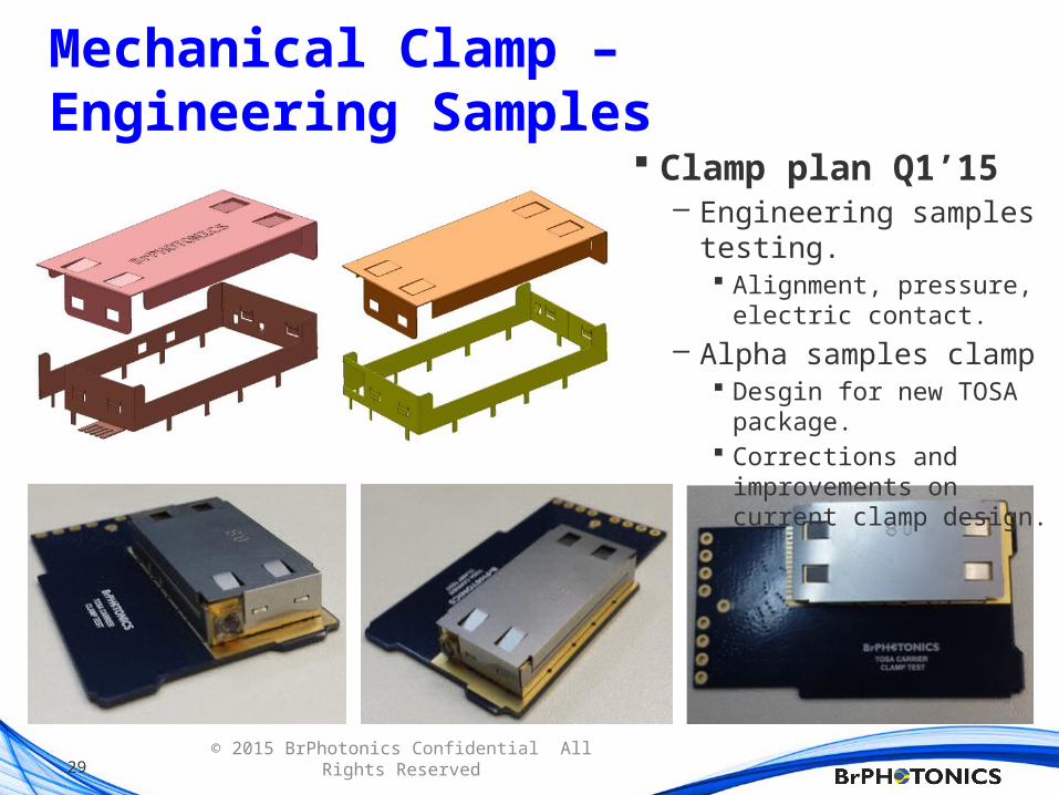
Mechanical Clamp – Engineering Samples
Clamp plan Q1’15– Engineering samples testing.
Alignment, pressure, electric contact.
– Alpha samples clamp Desgin for new TOSA package. Corrections and improvements
on current clamp design.

30 © 2015 BrPhotonics Confidential All Rights Reserved
Evaluation KitEvaluation Board (EVB)
TOSA Carrier PCB
TOSA on carrier
TOSA EVK assembled

31 © 2015 BrPhotonics Confidential All Rights Reserved
Real-time 100/200 G CFP2-ACO TOSA validation
ClariPhy CL20010Coherent ASIC
BrPhotonics 100GCFP2-ACO TOSA

32 © 2015 BrPhotonics Confidential All Rights Reserved
10 12 14 16 18 20 22 24 26 28 30-8
-7
-6
-5
-4
-3
-2
OSNR [dB/0.1 nm]
log1
0(B
ER
)
3.8e-3 BER
2.0e-2 BER
2.4e-2 BER
100G Theory
LiNbO3 Real-time
TOSA Real-time
100G OSNR tolerance (real-time validation)
Required OSNR– SD-FEC (2.4e-2)
LiNbO3: 11.6 dB TOSA: 11.8 dB
Small TOSA penalty (0.2 dB) in comparison with a LiNbO3 transmitter at SD-FEC limit.
Observations:• Same coherent DSP ASIC
and ICR used in both tests.• Bandwidth-limited (~15 GHz)
PCB can be improved to enhance TOSA performance.
BrP 100G TOSA vs LiNbO3 Transmitter
32-GBd DP-QPSK real-timewith coherent DSP ASIC

33 © 2015 BrPhotonics Confidential All Rights Reserved
200G DP-16QAM real-time validation
Required OSNR @ SD-FEC (2.0e-2):– BrPhotonics ACO-TOSA: 19.0 dB
Penalty with respect to theory ~2.0 dB.– LiNbO3 reference transmitter: 19.0 dB (literature)
16 18 20 22 24 26 28 30 32 34-4
-3.5
-3
-2.5
-2
-1.5
OSNR [dB/0.1 nm]
log1
0(B
ER
)
2.0e-2 BER
2.4e-2 BER
200G Theory
LiNbO3 (Literature)
TOSA Real-Time

34 © 2015 BrPhotonics Confidential All Rights Reserved
Ultra-Thin 100G DPQPSK Modulator package
Features: 2.33mm total height Designed to fit the gap clearance between pcb
and CFP2 cover Very versatile optical ports configuration (7) Optimal design for efficient fiber routings inside
CFP2 Very versatile solderless LGA or Solder pins
interconnections options Package footprint: L38.60 x W11.30 mm

35 © 2015 BrPhotonics Confidential All Rights Reserved
UT-M placement inside a CFP2 module
UT-M package height = 2.3mm
UT-M package module is designed to be placed between the CFP2 pcb and cover
UT-M package Suitable gap between PCB and Cover = 2.47mm
CFP2 PCB
CFP2 cover
36 © 2015 BrPhotonics Confidential All Rights Reserved
Rth
Y
X
I
Q
I
VXQp
VXQn
VXIpVXIn
Bias
YQ
I GN
D
Bias
Y G
ND
Bias
YQ
Bias
YI
Bias
Y
Bias XQI G
ND
Bias X GN
D
Bias XQ
Bias XI
Bias X
PD Y
(TM
) A
PD Y
(TM
) K
PD X (TE) K
PD X (TE) A
Rth
Q
VYQ
nVY
Qp
VYIn
VYIp
GN
D
LO OUT
IN
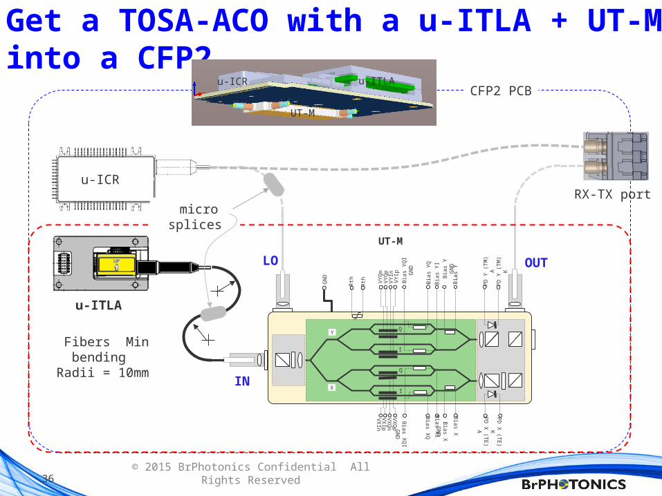
Get a TOSA-ACO with a u-ITLA + UT-M into a CFP2
Fibers Min bending Radii = 10mm
u-ITLA
u-ICRRX-TX port
micro splices
CFP2 PCBu-ICR u-ITLA
UT-M
UT-M

37 © 2015 BrPhotonics Confidential All Rights Reserved
UT-M internal layout and module placement inside CFP2
CFP2 - PCB
100G
UT-M
Quad DD
OUT
IN
LO
RF in
puts
DC co
ntro
ls
OUT
IN
LOLX8242 chip
50 TRRF IN
POL-MUX Optics
Input optics
RF inputs
DC contro
ls
Pre-assembled sub mount
lid
PM fiber collimators
SMF fiber collimators
Multilayer Ceramic
Hermetic package
RF inputs
DC controls

38 © 2015 BrPhotonics Confidential All Rights Reserved
Silicon Photonics - Tapeout timeline (CPqD/BrP)
March 2013
July 2013
October 2013
March 2014
June 2014
October 2014
DP-QPSK Modulator v1OpSIS/IME5x5 mm²SOI
DP-QPSK Receiver v1OpSIS/IME2.5x5 mm²SOI
Dynamic GFF HHI
4x6 mm²InP
DP-QPSK Modulator v2OpSIS/IME
5x5 mm²SOI
Si/TFPS ModulatorExternal Cavity Laser
IME3x16 mm²
SOI
DP-QPSK Receiver v2IME3x16 mm²SOI
Edge CouplersLETI4.2x4.7 mm²SOI

39 © 2015 BrPhotonics Confidential All Rights Reserved
BrPhotonics Passive Devices
Passive Components:• 1D Grating Coupler• 2D Polarization Splitter Grating Coupler (PSGC)• 90° Hybrid • Crossings • Edge Coupler to gain chip laser • Mach Zehnder Interferometers • MMI 2x2 50:50 • OSNR Monitor (interferometer) • Polarization Splitter Rotator (PSR) • Ring Resonator • Bragg mirror • Static dephaser • TAP 90:10 • TAP 99:1 • Y splitter 1x2

40 © 2015 BrPhotonics Confidential All Rights Reserved
BrPhotonics Active Devices
Active Components:
• 2nd and 3rd Order Ring Tunable Filters
• Photodiode
• PIN Modulator - VOA
• RF termination (33Ω)
• Ring Resonator Modulator• • Silicon tunable cavity laser
• Thermal Phase Shifter
• Traveling Wave Mach Zehnder
Buried oxide
Ge
Si

41 © 2015 BrPhotonics Confidential All Rights Reserved
Silicon photonics 100G Receiver
Silicon Chip Characterization (w/o TIAs)
CoherentReceiver
Signal
EDFA
ASE
VOA
Filter Coupler 99:1
PC
OSA
ECL
PC
XQ
YI
YQ
XI
Oscilloscope DSP
2.5 x 5 mm2

42 © 2015 BrPhotonics Confidential All Rights Reserved
Silicon Photonics IP List/Status

43 © 2015 BrPhotonics Confidential All Rights Reserved4343 © 2013 GigOptix, Inc. Confidential All Rights Reserved
Microlectronic IPs and ASIC Development

44 © 2015 BrPhotonics Confidential All Rights Reserved
Microelectronics for Optical Communications OTN ASIC
– Single chip solution Mapper/Framer/Criptography/FEC for 100G
40nm TSMC Test Chip

45 © 2015 BrPhotonics Confidential All Rights Reserved
OTN IP List/Status

46 © 2015 BrPhotonics Confidential All Rights Reserved
Microelectronics for Optical Communications DSP ASIC– Single chip 400G 64 to 16 QAM/QPSK up to 45GBd
16nm FF+ TSMC Test Chip
LineModem
(DSP)
OTU4Framer
ClientMapper
Line 2
Host
LineAFE
Register File
EmbeddedµP
Real-TimeCapture RAM
SPI
HIHQVIVQ
MDIO
20 x 25G10 x 50G Ho
st Se
rdes
Cros
sbar
Sw
itch
and
Gear
box
OTUx
LineModem
(DSP)OTUx
HIHQVIVQ
Line 1
LineAFE
25G Serial
FEC
FEC
OTU4Framer
ClientMapper
OTU4Framer
ClientMapper
OTU4Framer
ClientMapper
OTU4Framer
ClientMapper
ADC_I
ADC_Q
DAC_I
DAC_Q
AFE INTERFACE DSP
DAC_I 128X8
DAC_Q 128X8
ADC_I 128X8
ADC_Q 128x8
DSP_I_IN 128X8
DSP_Q_IN 128X8
DSP_OUT 64X4
AHB MASTER
SPI I
F
ADC_I CNTRL/STATUS
ADC_Q CNTRL/STATUS
ADC_I_CLK
ADC_Q_CLK
DAC_I CNTRL/STATUS
DAC_Q CNTRL/STATUS
DAC_I_CLK
DAC_Q_CLK
AFE_
AHBL
_IF
/32
/32
DSP_RX_CLK
DSP_TX_CLK
TST_BUSI_OUT_128X8
AFE
_RST
_N
DSP
_RST
_N
PMONPMON IF
AFE
ADC_HI_P
ADC_HI_N
ADC_QI_P
ADC_QI_N
DAC_HI_P
DAC_HI_N
DAC_HQ_P
DAC_HQ_N TST_BUSQ_OUT_128X8
Osc(Need to
Spec)
CSR_INTERFACE
SCLK
OSC_P
OSC_N
700MHz
RXPLL
TXPLL
16GHz
16GHz
700M
Hz
DIV32_BYPASS
DIV32_BYPASS
PLL_BYPASS
PLL_BYPASS
Full ASIC Arch.
DSP Test Chip IPs- TR- PE- Demapper- MUX

47 © 2015 BrPhotonics Confidential All Rights Reserved
DSP IP List/Status

48 © 2015 BrPhotonics Confidential All Rights Reserved
Tunable LASER – Narrow Linewidth
New Project starting joint with CPqD between BrP/PADTEC with BNDES support, targeting complete verticalization in coherent transcievers applications
Main Specs:Linewidth <100KHz
Pdiss <4W
Applications:CoC
GoldBoxuITLA
Tunable LASER + Modulator + Receiver integrated in a single packaging : 100/200G TROSA CFP4

49 © 2015 BrPhotonics Confidential All Rights Reserved
100G/200G CFP2/ACO is happening now!!!
400G Modules first introduction

50 © 2015 BrPhotonics Confidential All Rights Reserved
First Product Demo at OFC 2014
100G Coherent TOSA based on TFPS Modulator
51 © 2015 BrPhotonics Confidential All Rights Reserved
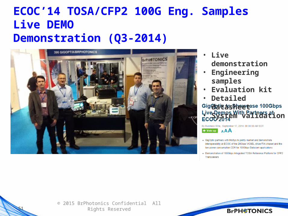
ECOC’14 TOSA/CFP2 100G Eng. Samples Live DEMO Demonstration (Q3-2014)
• Live demonstration• Engineering samples• Evaluation kit• Detailed datasheet• System validation

52 © 2015 BrPhotonics Confidential All Rights Reserved
OFC’15 TOSA 200G DP-16QAM Real Time Live DEMO
Next Phase ... Telcordia qualification, running now!!!

53 © 2015 BrPhotonics Confidential All Rights Reserved
BrPhotonics - Product Roadmap Overview
2013
Potential
ASIC OTN 100GFramer + Crypto.
+ Storage
LM8242Polymer
IQ Dual Pol.Modulator
SRX-04-28-01SRX-02-56-01
SiPh Coherent Rx.
LTO-04-28-01100G TOSA CFP2
WRO-04-28-01100G ROSA CFP2
SM-04-28-01SiPh IQ
Dual Pol.Modulator
SM-16-28-01400G Dual
Carrier DualPol . IQ
Modulator Si-TFPS
1T NxCarrierDual Pol . IQModulator
SiliconProven IPsOTN 100G(Test Chip)
Silicon Proven DSP IPs
(Test Chip)
40nm TSMC
16nm TSMCSilicon Proven
DSP IPs DSP100/400G(Full Chip)
2014 2015 2016 2017 >2017
Planned
4x28G
2x56Gor
16QAM
Microelectronics
Sub-Assembly & Tunable LASER
Tx/Rx Chips
1T NxCarrierCoherentReceiver
STO-04-28-01Single Packg.
100G TOSA+ROSA CFP4
STO-04-28-01400G Dual TOSA
CFP2
SM-04-28-01Si-TFPS Dual Pol.
Modulator
SM-04-28-01Si-TFPS Dual Pol.
Receiver
WRO-04-28-02400G Dual ROSA
CFP2
Planned
LM8242Polymer
IQ Dual Pol.Modulator
LM8242Polymer
IQ Dual Pol.Modulator Packaged
TL-01-28-01CoC Coherent Tunable LASER

54 © 2015 BrPhotonics Confidential All Rights Reserved
Future Applications
Multi Carrier 400G/1T– Chip Level
Single chip solutions for multicarrier applications
– Packaging Level Modular solution
supporting TOSA, ROSA, TROSA and interconnec.
– System Level Controllers (Bias, LASER,
Driver) miniaturized and scalable
Datacom/Datacenter– 100G already arrive in
datacenter (10x10 and 4x25)
– Single 100G is expected in a near future supported by high freq. Optics and electronics (70 GHz) or through deep coherent price reduction (mainly DSP)

55 © 2015 BrPhotonics Confidential All Rights Reserved
Final Considerations
High speed integrated optics for 100G and beyond is entering in the Market (100G CFP2 modules)
Device integration is mandatory to track this evolution demanding increasing bit rates
BrPhotonics has a clear ROADMAP verticalizing device level targeting support 100G and beyond transciever Market to world wide market
Brazilian echosystem is supportive to high tech companies with tech. background and solid market view (FUNTTEL, FINEP, BNDEs, private investors, ...)

© 2015 BrPhotonics Confidential All Rights Reserved
www.brphotonics.com