Embed Size (px)
Citation preview
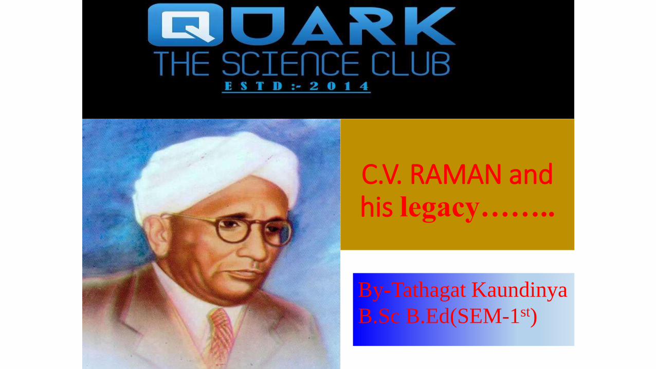
C.V. RAMAN and his legacy……..
By-Tathagat Kaundinya
B.Sc B.Ed(SEM-1st)

HIS EARLY LIFE
•Born on 7th NOV,1888 in Thiruvanaikkaval near Trichinopoly, Tamilnadu.
•MOTHER- (Late) Parvati Ammal
•FATHER- (Late) Chandrasekhara Iyer, was a school teacher.
•Raman’s parents had eight childrens (5 sons and 3 daughter). Raman was their second child.
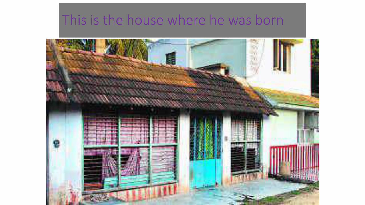
This is the house where he was born

EARLY EDUCATION
• At early age, Raman moved to the city of Visakhapatnam, and studied in St. Aloysius Anglo-Indian high school.
• Raman passed his matriculation examination at the age of eleven and passed His F.A. examination equivalent to today’s intermediate exam with a scholarship at the age of thirteen.
• In 1902 he joined Presidency College in Madras where his father became a lecturer in mathematics and physics.
Education continues…..
• In 1904 he passed his B.A.(Bachelor of Arts) examination-he stood first and won gold medal in physics.
• When Raman completed his B.A. he was suggested to go to England for his further studies. However ,he was rejected , since Civil Surgeon of Madras did not find him physically fit to go to England.
• In 1907 he gained his M.A.(Master of Arts) degree with the highest distinction .
• After he completed his M.A., he took the Civil Services competitive exam for the Finance Department. Sure enough, he topped the score in that exam.
CAREER
• He went to Calcutta to join the Finance Department there as an Assistant Accountant General. Within a week of his reaching Calcutta, he noticed, while he was on his way to work, a sign board which read "The Indian Association for Cultivation of Sciences", and this was to play a major role in his life, and in the very history of scientific culture in our country.
• In 1917,Raman resigned from his government service after was appointed the first Palit Professor of Physics at the University of Calcutta.
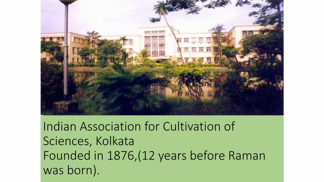
Indian Association for Cultivation of Sciences, Kolkata Founded in 1876,(12 years before Raman was born).
HIS ACHIEVEMENTS
• On his sea voyage to Europe, Raman was struck by the blueness ofthe sea. Many of us believe that the blueness of the sea is due to theblueness of the sky.
Lord Rayleigh himself said "the much admired blueness of the sea... is simply the blue of the sky seen by reflection”
Rayleigh, as many of you would know, is the one who gave the firstcorrect explanation for the sky being blue. .
Professor Raman did a simple experiment on his European voyagewhile on the ship and found that the blueness of the sea was notmerely the blue of the sky seen by reflection, as Lord Rayleigh hadmaintained; rather, the blue of the sea was due to molecularscattering by the waters of the ocean. It was an extra-ordinary sighton the ship to see this turbaned Indian scientist conducting hisexperiments on the ship's deck with a simple polarizing nicol prismon sample's of sea water!

• This was in a sense the beginning of the most outstandingexperiments ever performed in country, and lead to thework which brought the only prize in Physics our countryhas received.
• Returning to India, Raman initiated research on 3 differentlines:
1) The scattering of light by liquids,
2) The scattering of x-rays by liquids,
3) The viscosity of liquids.
• Professor Raman's work on the scattering of light byliquids of course was the one which fetched him, and ourcountry, the Nobel prize in Physics and came to be knownas the RAMAN EFFECT.
HIS ACHIEVEMENTS - Continues
HONOURS AND AWARDS
Raman was Honored with a large number of honorarydoctorates and memberships of scientific societies:-
• he was elected a fellow of the royal society early in hiscareer(1924) and knight bachelor in 1929.
• In 1930 he won the noble Nobel prize in physics.
• In 1930 he won Hughes medal.
• In 1941 he was awarded the Franklin medal.
• In 1954 he was awarded the Bharat Ratna.
• He was awarded the Lenin Peace Prize in 1957.
India celebrates National science day on 28 February ofevery year to commemorate the discovery of the Raman effect in1928.

POSTHUMOUS RECOGNITION AND CNTEMPORARY REFERENCES:-• On 7 Nov 2013, google doodle honoured C.V. Raman on his 125th
birthday.
• A road in India’s capital (New Delhi) is named c.v. Raman Marg.
• An area in Bangalore near 16th cross road is called C.V. Raman Nagar.
• The road running north of the national seminar complex Bangalore (India) is named C.V. Raman road .
• A building in the Indian Institute of Science (Bangalore) is named “ Raman building”.
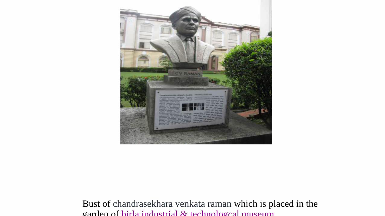
Bust of chandrasekhara venkata raman which is placed in the garden of birla industrial & technologcal museum.

DEATH
• At the end of October 1970 he collapsed in his laboratory, the valve of his heart having given way. He was moved to hospital and the doctors gave him four hours to live. He survived and after a few days refused to stay in the hospital as he preferred to stay in the garden of his institute surrounded by flowers.
• Two days before he died, he told one of his former students,“Do not allow the journals of the academy to die, for they are the sensitiveindicators of the quality of science being done in the country and whetherscience is taking root in it or not”.• That same evening ,Raman met with the board of management of his
institute and (from his bed) with them any proceedings with regards to the institute’s management.
• He died from natural causes early next morning on 21 Nov 1970.

His legacy continues….

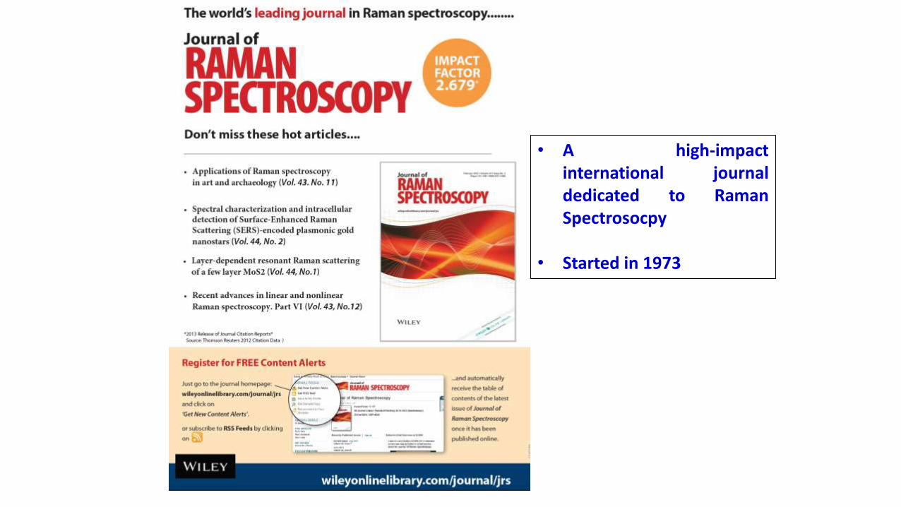
• A high-impactinternational journaldedicated to RamanSpectrosocpy
• Started in 1973
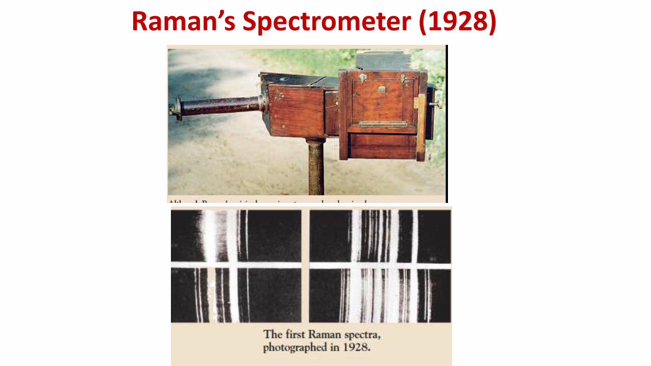
Raman’s Spectrometer (1928)
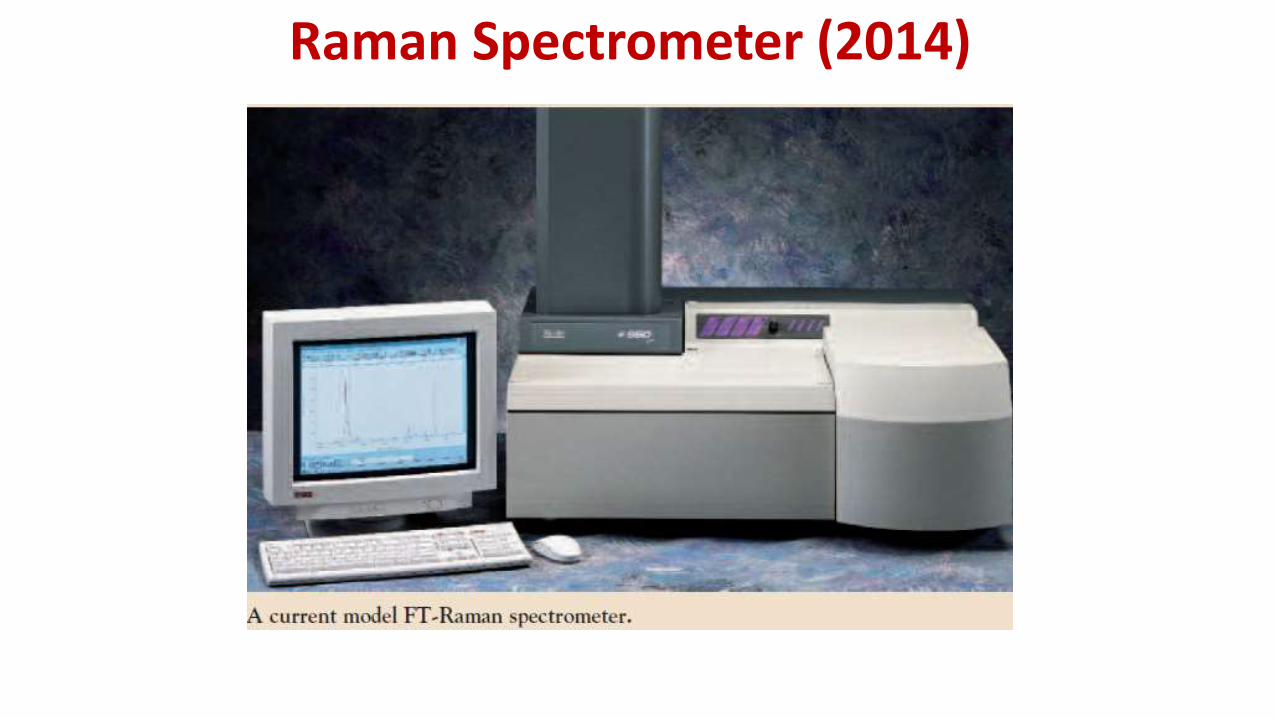
Raman Spectrometer (2014)

Raman spectroscopy provides information
about molecular vibrations
Symmetric Stretching Asymmetric Stretching Wagging
Twisting Scissoring Rocking

Raman spectroscopy provides information
about molecular vibrations

Raman spectroscopy provides information
about molecular vibrations
Energy level diagram for Rayleigh and Raman scattering.

Raman spectroscopy provides information
about molecular vibrations
Methyl ester of oleic acid
Raman Spectroscopy as a Chemist’s Tool
Principal method of non-destructive analysis of organic and inorganic compounds(Provides information about what is present and how much is present.)
used to monior manufactuing process in petroleum and pharmaceutical industries.
Illegal drugs can be analyzed without breaking the evidence seal over the
plastic bag
Nuclear waste materials can be analyzed from a safe distance using a fibre optic Raman probe
Laser Raman techniques to record the spectra of transient chemical species with lifetimes as small as 10 –11 seconds.
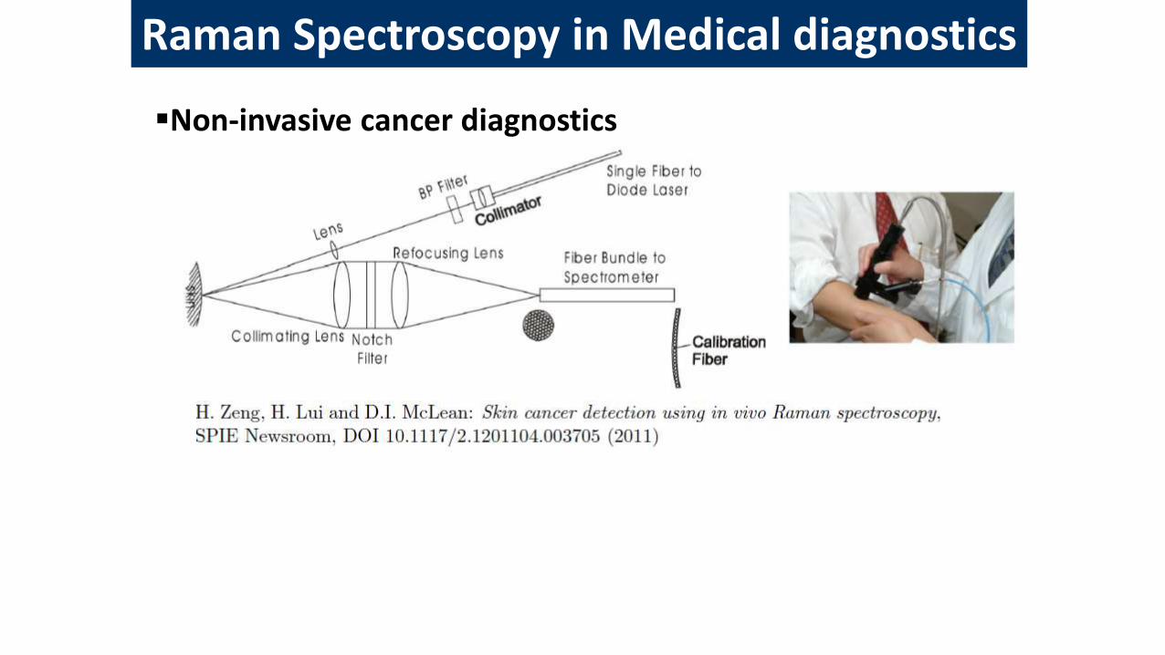
Raman Spectroscopy in Medical diagnostics
Non-invasive cancer diagnostics

Raman Spectroscopy in Forensic science
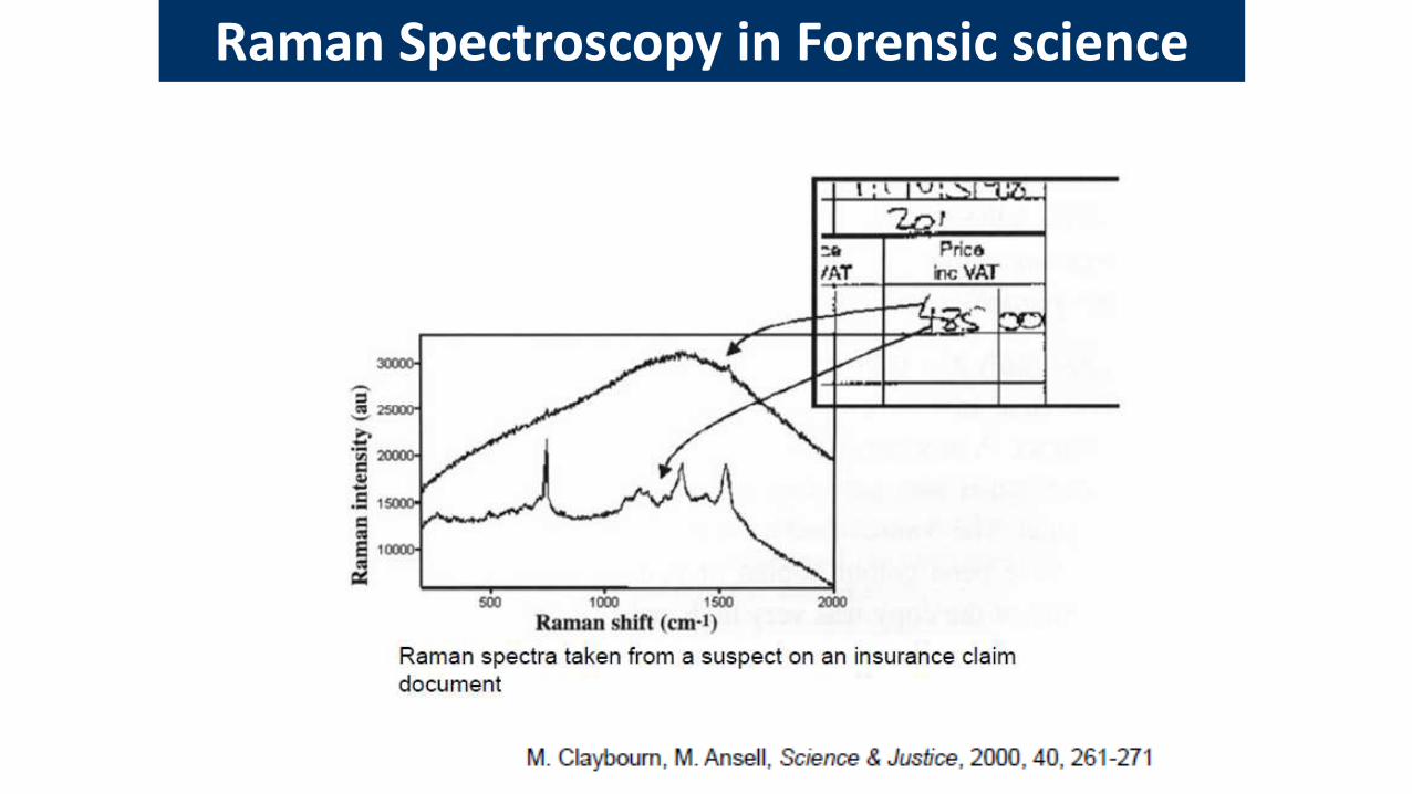
Raman Spectroscopy in Forensic science
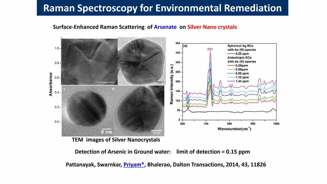
Raman Spectroscopy for Environmental Remediation
Detection of Arsenic in Ground water: limit of detection = 0.15 ppm
Pattanayak, Swarnkar, Priyam*, Bhalerao, Dalton Transactions, 2014, 43, 11826
Surface-Enhanced Raman Scattering of Arsenate on Silver Nano crystals
TEM images of Silver Nanocrystals

Raman Spectroscopy for Environmental Remediation
Satarupa Pattanayak, Abhishek Swarnkar, Amiya Priyam, Gopal M. Bhalerao
PhD Student UG summer internCollaborator from
UGC-DAE CSR, Kalpakkam

Fundamentals Raman Spectroscopy
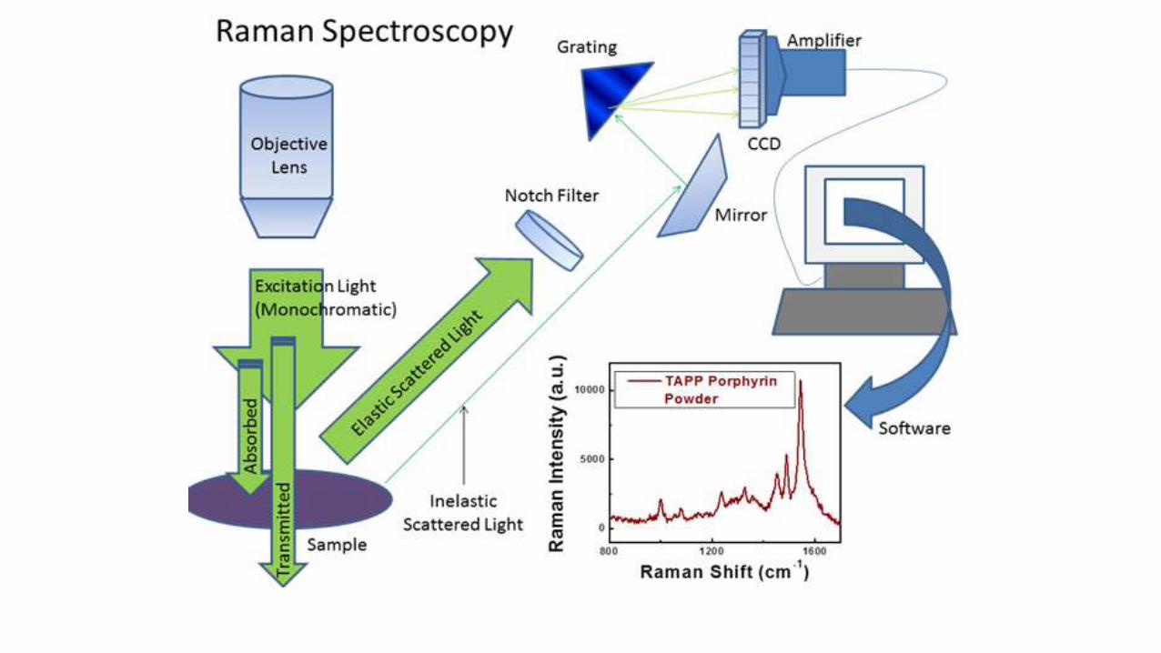
• When radiation passes through a transparent medium, the species present scatter a fraction of
the beam in all directions.
• In 1928, the Indian physicist C. V. Raman discovered that the visible wavelength of a small
fraction of the radiation scattered by certain molecules differs from that of the incident beam
and furthermore that the shifts in wavelength depend upon the chemical structure of the
molecules responsible for the scattering.
• Raman spectra are acquired by irradiating a sample with a powerful laser source of visible
radiation (λ).
• During irradiation, the spectrum of the scattered radiation (λ1) is measured at some angle (often
900 ) with a suitable spectrometer.
• At the very most, the intensities of Raman lines are 0.001 % of the intensity of the source.
Raman shift -> colloquial use->
wavenumbers: ∆𝜔 =1
λ−
1
λ1
∆𝜔(𝑐𝑚−1) =1
λ (𝑛𝑚)−
1
λ1(𝑛𝑚)×(107 𝑛𝑚)
𝑐𝑚

31
3-features of Raman scattering: 1. Stokes 2. Anti-stokes, and 3. Rayleigh

ZnO fundamentals Group II-VI binary compound semiconductor
3-types of crystal structures: Each anion is surrounded by 4 cations, & vice versa
(1) Rocksalt (2) zinc blende (3) Wurtzite- stable at RT
Zn
O
[1] H. Morkoç et al., Zinc Oxide-Fundamentals, Materials and Device Technology, Wiley-VCH
H. Matsui & H. Tabata
Nanowires book, ISBN
9789537619794
www.intechopen.com
http://commons.wikimedia.org/wiki/File:Wurtzite_polyhedra.png
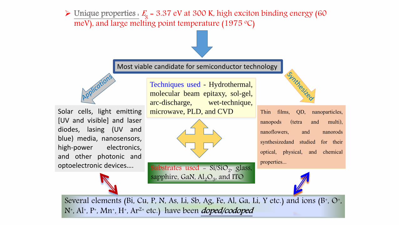
Unique properties : Eg = 3.37 eV at 300 K, high exciton binding energy (60 meV), and large melting point temperature (1975 oC)
Most viable candidate for semiconductor technology
Solar cells, light emitting[UV and visible] and laserdiodes, lasing (UV andblue) media, nanosensors,high-power electronics,and other photonic andoptoelectronic devices….
Thin films, QD, nanoparticles,nanopods (tetra and multi),nanoflowers, and nanorodssynthesizedand studied for theiroptical, physical, and chemicalproperties...
Techniques used - Hydrothermal,
molecular beam epitaxy, sol-gel,
arc-discharge, wet-technique,
microwave, PLD, and CVD
Substrates used - Si/SiO2, glass,sapphire, GaN, Al2O3, and ITO
Several elements (Bi, Cu, P, N, As, Li, Sb, Ag, Fe, Al, Ga, Li, Y etc.) and ions (B+, O+,N+, Al+, P+, Mn+, H+, Ar2+ etc.) have been doped/codoped
𝑪𝟔𝒗𝟒 (P63mc) space group
8 sets of phonon modes at the Γ point of Brillouin zone
Γ = 2 × (A1 + B1 + E1 + E2)
Two Acoustic: Γaco = A1 +E1
Six Optical: Γopt = A1 + (2 × B1) + E1+ (2 × E2)
Γopt are involved in the Raman scatteringB1 modes are both Raman and infrared inactive (silent)
A1 : A1(TO) , A1(LO) ; E1 : E1(TO), E1(LO)
E2 modes: low (E2low) and high (E
2high
)Phonon dispersion curve
[1] H. Morkoç et al., Zinc Oxide-Fundamentals, Materials and Device Technology, Wiley-VCH
http://en.wikipedia.org/wiki/File:Brillouin_zone_in_hexagonal_lattice.png
Symmetry, Group theory, and ZnO
[1] H. Morkoç et al., Zinc Oxide-Fundamentals, Materials and Device Technology, Wiley-VCH
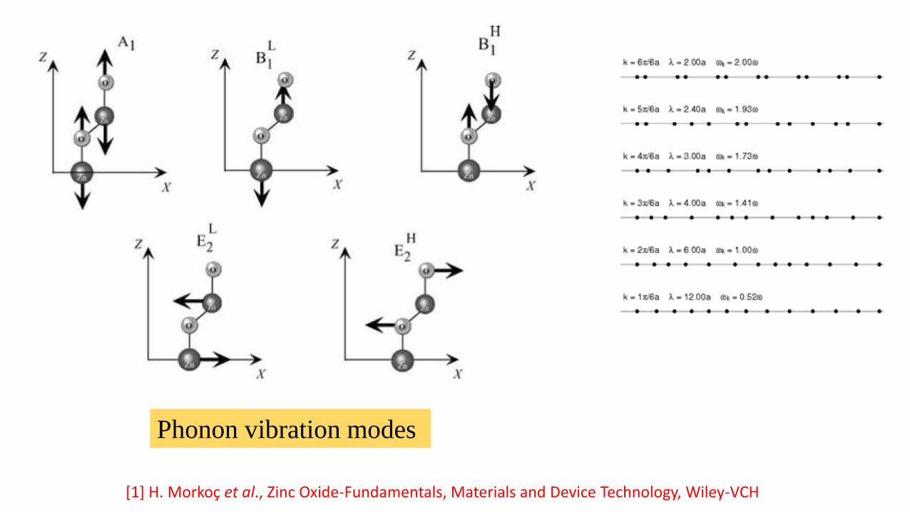
Phonon vibration modes
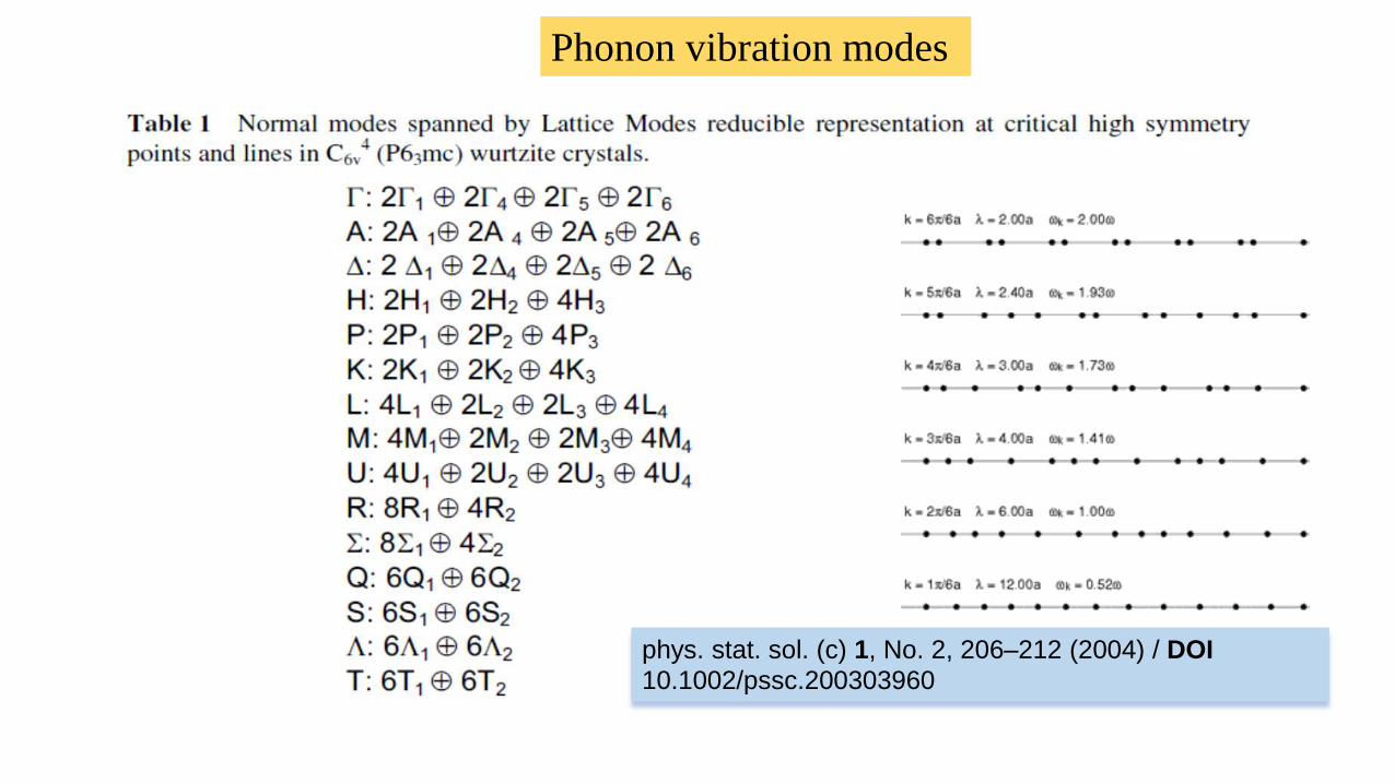
phys. stat. sol. (c) 1, No. 2, 206–212 (2004) / DOI
10.1002/pssc.200303960
Phonon vibration modes
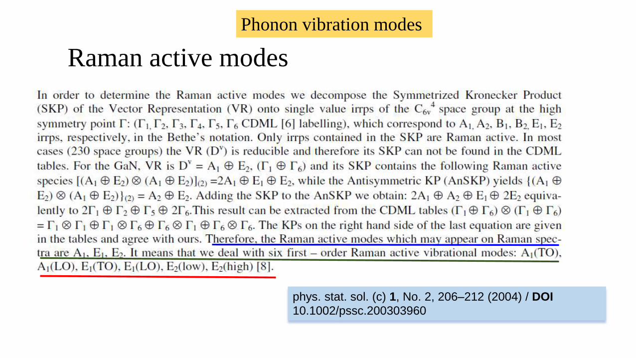
Raman active modes
phys. stat. sol. (c) 1, No. 2, 206–212 (2004) / DOI
10.1002/pssc.200303960
Phonon vibration modes
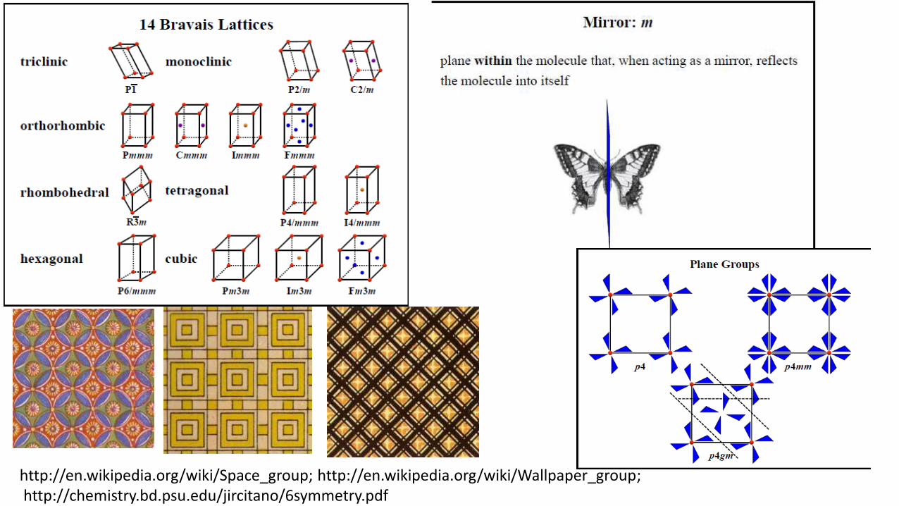
http://en.wikipedia.org/wiki/Space_group; http://en.wikipedia.org/wiki/Wallpaper_group;http://chemistry.bd.psu.edu/jircitano/6symmetry.pdf

Called a monument to love, the Taj Mahal has also been called "India's
most famous and finest example of architecture. We could call it a
monument to symmetry. From the formal gardens divided into four
sections, to the tomb 900 feet from the entrance, the four minarets
continue this symmetrical theme. The minarets next to the Taj Mahal are
41.1 meters or 137 feet high and are cylindrical columns with beveled
angles. Located at each of the corners of the raised marble plinth the
minarets repeat the right angles that are an obvious part of the Taj
Mahal. The main structure is cubical. The windows have arches which
comes to a point. The windows create arched recesses which are
perfectly arranged on both stories. The central circle at the base arches
upward to create the famous onion dome. The Taj Mahal is a fine
example of geometry. Like all buildings the Taj Mahal is a combination
of planes. The rectangular reflecting pool mirrors the pools in each of
the four gardens and makes your eyes follow alongparallel lines to the
tomb's entrance. The intersecting perpendicular lines continue to
create right angles in each of the four sections which are subdivided into
another four squares. The doorways are rectangular in design with semi-
octagonal angles. The room that the tombs are placed is octagonal. As
you look at the Taj Mahal, there are multiple lines of symmetry. The
entire complex is laid out in quadrilaterals. The total effect combines
to make one of rhythm and harmony.
Google images; http://www.cultural-heritage-india.com/gifs/taj-mahal-in-india.jpg
200 250 300 350 400 450 500 550 600 650 700 750 800
300
600
900
1200
1500
1800
(iv)(iii)
(ii)
(i)
E1(T
O)
(412 c
m-1
)
A1(T
O)
(382 c
m-1
)
2E
low
2 (
201 c
m-1
)
Ehig
h
2-
Elo
w
2(3
32 c
m-1
)
Si substrate (519.45 cm-1
)
Ram
an I
nte
nsi
ty (
a.u
)
Wavenumber (cm-1)
Undopeed ZnO nanorods (i)
1 ~ 1.5 * 108 ions/cm2(ii)
2 ~ 5.5 * 108 ions/cm2(iii)
3 ~ 9 * 108 ions/cm2(iv)
Bi74+ on ZnO nanorodsEhigh
2 (437.36 cm
-1)
A1(L
O)
(578 c
m-1
)
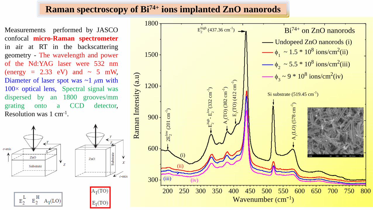
Measurements performed by JASCO
confocal micro-Raman spectrometer
in air at RT in the backscattering
geometry - The wavelength and power
of the Nd:YAG laser were 532 nm
(energy = 2.33 eV) and ~ 5 mW,
Diameter of laser spot was ~1 μm with
100× optical lens, Spectral signal was
dispersed by an 1800 grooves/mm
grating onto a CCD detector,
Resolution was 1 cm-1.
Raman spectroscopy of Bi74+ ions implanted ZnO nanorods
200 250 300 350 400 450 500 550 600 650 700 750 800
300
600
900
1200
1500
1800
(iv)(iii)
(ii)
(i)
E1(T
O)
(41
2 c
m-1
)
A1(T
O)
(38
2 c
m-1
)
2E
low
2 (
20
1 c
m-1
)
Ehig
h
2-
Elo
w
2(3
32
cm
-1)
Si substrate (519.45 cm-1
)
Ram
an I
nte
nsi
ty (
a.u
)
Wavenumber (cm-1)
Undopeed ZnO nanorods (i)
1 ~ 1.5 * 108 ions/cm2(ii)
2 ~ 5.5 * 108 ions/cm2(iii)
3 ~ 9 * 108 ions/cm2(iv)
Bi74+ on ZnO nanorodsEhigh
2 (437.36 cm
-1)
A1(L
O)
(57
8 c
m-1
)
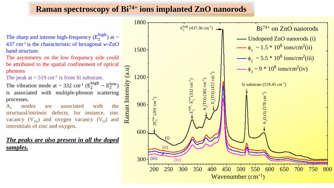
The sharp and intense high-frequency (E2high
) at ~
437 cm-1 is the characteristic of hexagonal w-ZnO
band structure.
The asymmetry on the low frequency side could
be attributed to the spatial confinement of optical
phonons
The peak at ~ 519 cm-1 is from Si substrate.
The vibration mode at ~ 332 cm-1 (E2high
− E2low)
is associated with multiple-phonon scattering
processes.
A1 modes are associated with the
structural/intrinsic defects, for instance, zinc
vacancy (VZn) and oxygen vacancy (VO) and
interstitials of zinc and oxygen.
The peaks are also present in all the doped
samples.
Raman spectroscopy of Bi74+ ions implanted ZnO nanorods
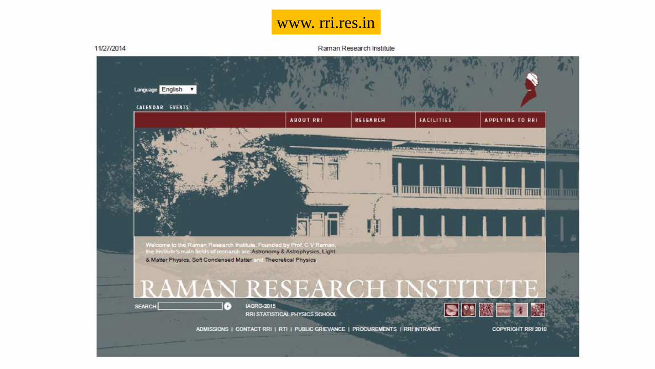
www. rri.res.in
Raman Research Institute - Overview
The Raman Research Institute was founded in 1948 by the Indian physicist and Nobel Laureate, Sir
C V Raman, to continue his studies and basic research after he retired from the Indian Institute of
Science. Sir C V Raman served as its director carrying on his personal research until his demise in
1970. It was funded personally by him and with donations from private sources.
History
In December 1934, the Government of Mysore gifted a plot of land in Bangalore to Professor Raman
for the creation of a research institute. In the same year, the Indian Academy of Sciences was
founded by Prof. Raman. Some years following the creation of the Raman Research Institute in
1948, Prof. Raman made a gift of various movable and immovable properties to the Academy for the
use and benefit of the Raman Research Institute. After the Professor's demise in November 1970,
the Academy created a public charitable trust: the Raman Research Institute Trust. The lands,
buildings, deposits, securities, bank deposits, moneys, laboratories, instruments, and all other
movable and immovable properties held by the Academy for the Raman Research Institute were
transferred to the RRI Trust. The foremost function of the RRI Trust was to maintain, conduct and
sustain the Raman Research Institute.
www.rri.res.in
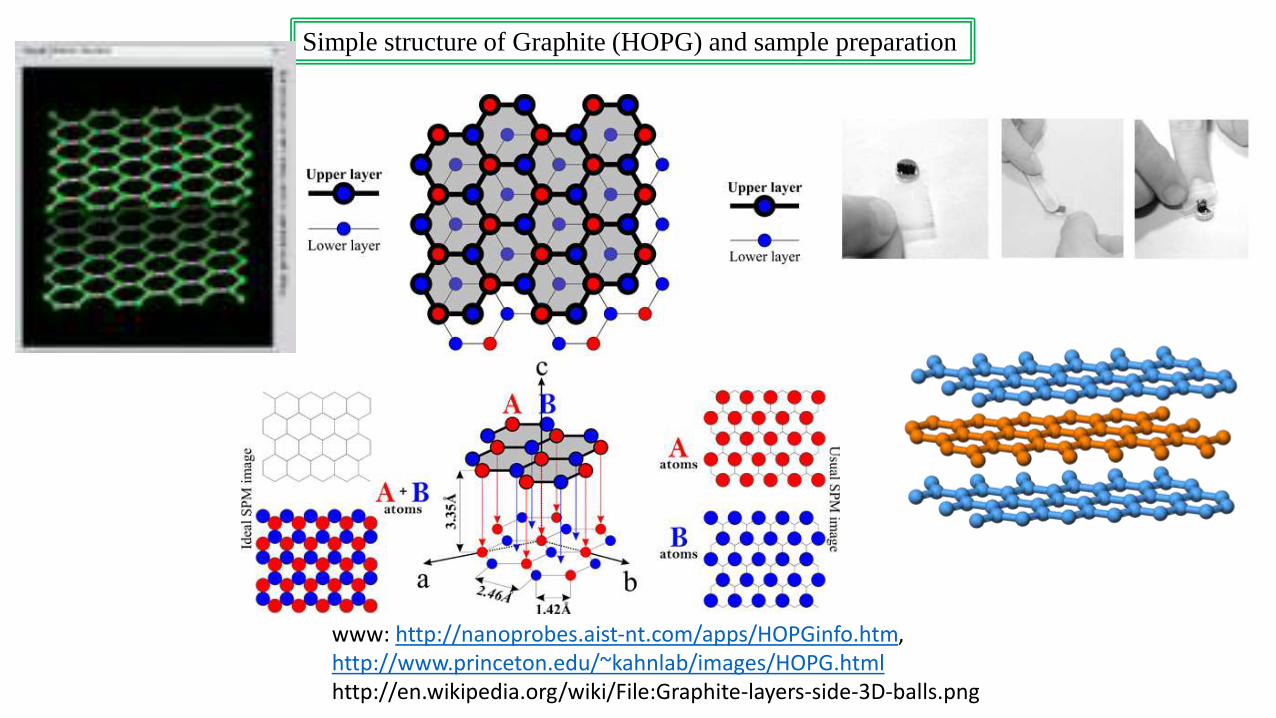
www: http://nanoprobes.aist-nt.com/apps/HOPGinfo.htm, http://www.princeton.edu/~kahnlab/images/HOPG.htmlhttp://en.wikipedia.org/wiki/File:Graphite-layers-side-3D-balls.png
Simple structure of Graphite (HOPG) and sample preparation

45
1000 1500 2000 2500 3000 35000
1000
2000
3000
4000
D peak
~ 1350 cm-1
G peak = E2g peak (~ 1580 cm-1)
2D or G' peak ~ 2721 cm-1
Inte
snit
y
Raman shift (cm-1)
Virgin HOPG
Raman spectrum of Graphite
The unirradiated and
irradiated samples
were analyzed by
JASCO Raman
spectrometer in air.
I. Laser -> (λ) 532 nm
(energy = 2.33 eV)
and power -> 5 mW
II. Spot -> 1 μm with
100× optical lens
III. Resolution of
instrument -> 1 cm-1
Future Plans
B.Sc.B.Ed. IVth Semester Physics Presentations (January-June 2015)
1. H.J. Bhabha –
2. Ramanujan –
3. S.N. Bose –
4. Maxwell –
(Speakers will be selected)
Vedic maths:
1-7 have been allotted.
Applications are invited for the remaining ones
B.Sc.B.Ed. IInd Semester Physics Presentations (January-June 2015)
Topics will be decided soon

Thank you
![Meditation [Dhyan] Versus Relaxation A Review With ... fileA Review With Comprehensive Bibliography Surekha D. Kaundinya*, Dilip V. Kaundinya** * Professor & Head- Physiology,**Ex-Prof](https://img.dokumen.tips/doc/110x75/5e177c627785c61c1a2af619/meditation-dhyan-versus-relaxation-a-review-with-review-with-comprehensive.jpg)


![Meditation [Dhyan] Versus Relaxation A Review With ...oaji.net/articles/2014/1021-1405155841.pdfA Review With Comprehensive Bibliography Surekha D. Kaundinya*, Dilip V. Kaundinya**](https://img.dokumen.tips/doc/110x75/5e177d73936f11634063115e/meditation-dhyan-versus-relaxation-a-review-with-oajinetarticles20141021-.jpg)