Embed Size (px)
Citation preview
Atomic Layer Deposition: a process technology for transparent conducting oxides
Paul Chalker
PV-CDT TCO Master class November 2014
Outline
• Introduction to atomic layer deposition processes
• In-situ monitoring
• Role of co-reagent - copper oxide based TCO
• Conformal 3D deposition - TiO2 in AAO templates
• Doping in atomic layer deposition - doped ZnO based TCO • Some conclusions
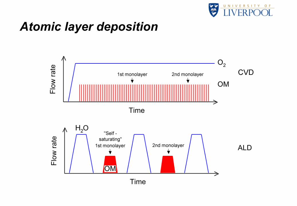
Atomic layer deposition
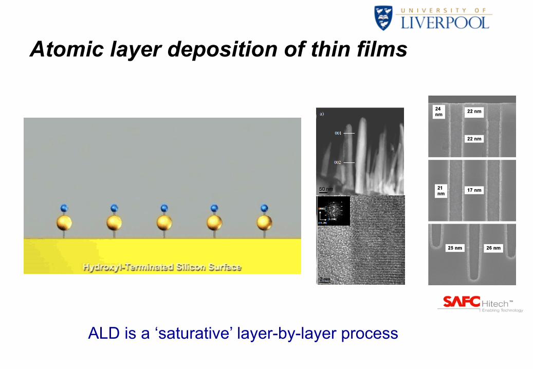
Atomic layer deposition of thin films
ALD is a ‘saturative’ layer-by-layer process
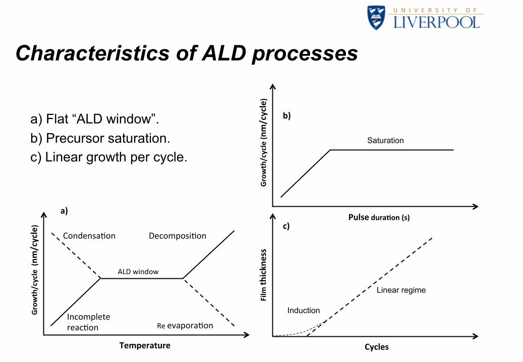
Characteristics of ALD processes
a) Flat “ALD window”. b) Precursor saturation. c) Linear growth per cycle.
Incomplete reac-on
Condensa-on
ALD window
Decomposi-on
Re evapora-on
Temperature
Growth/cycle (nm
/cycle)
Pulse dura8on (s)
Growth/cycle (nm/cycle)
Cycles
Film
thickn
ess
a)
b)
c)
Saturation
Induction
Linear regime
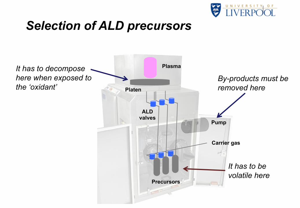
It has to be volatile here
By-products must be removed here
Selection of ALD precursors
Plasma
Platen
Precursors
ALD valves
Pump
Carrier gas
It has to decompose here when exposed to the ‘oxidant’
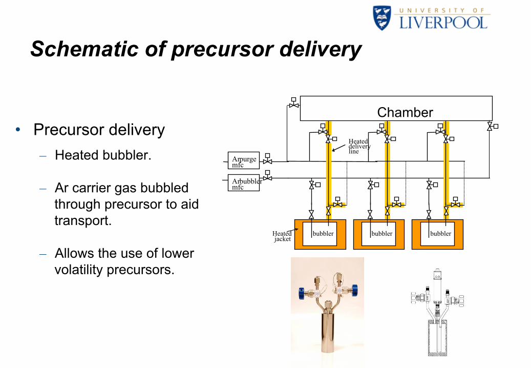
Schematic of precursor delivery
Heated delivery line
Heated jacket
Ar purge mfc Ar bubbler mfc
bubbler
Chamber
bubbler
bubbler
• Precursor delivery – Heated bubbler.
– Ar carrier gas bubbled through precursor to aid transport.
– Allows the use of lower volatility precursors.
8
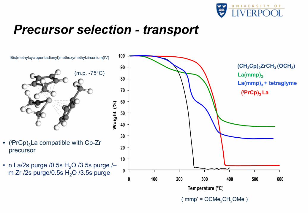
Precursor selection - transport
• (iPrCp)3La compatible with Cp-Zr precursor
• n La/2s purge /0.5s H2O /3.5s purge /– m Zr /2s purge/0.5s H2O /3.5s purge
( mmp’ = OCMe2CH2OMe )
0
10
20
30
40
50
60
70
80
90
100
0 100 200 300 400 500 600
We
igh
t (%
)
Temperature (°C)
(CH3Cp)2ZrCH3 (OCH3) Bis(methylcyclopentadienyl)methoxymethylzirconium(IV)
(iPrCp)3 La
(m.p. -75°C) La(mmp)3
La(mmp)3 + tetraglyme

In-situ monitoring methods
9
Quartz crystal microbalance (QCM) - measures a mass per unit area by measuring the change in frequency of a quartz (or GaPO4) crystal resonator. Sauerbrey equation
f0 – crystal natural resonant frequency (Hz), ρc - crystal density (g/cm3), µc is the crystal shear modulus (g/cm s2).
0" 50" 100" 150" 200" 250"
QCM
$mass$gain$(rel.)$
Time$(s)$
!" #!" $!!" $#!" %!!" %#!"
!"#$%&'"(%)'*")+,-'
./0)'*1-'
1s"
5s"
0" 50" 100" 150" 200" 250"
Growth$rate$(rel.)$
Time$(s)$
TMA"with"UV"
TMA"without"UV"
UV"without"TMA"
1"cycle"
UV"on"
Δm

In-situ monitoring methods
10
In-situ spectroscopic ellipsometry (SE) - measures a change in polarization as light reflects or transmits from a material structure. The polarization change is represented as an amplitude ratio, Ψ, and the phase difference, Δ.
Sr
Hf
SHfO3
11
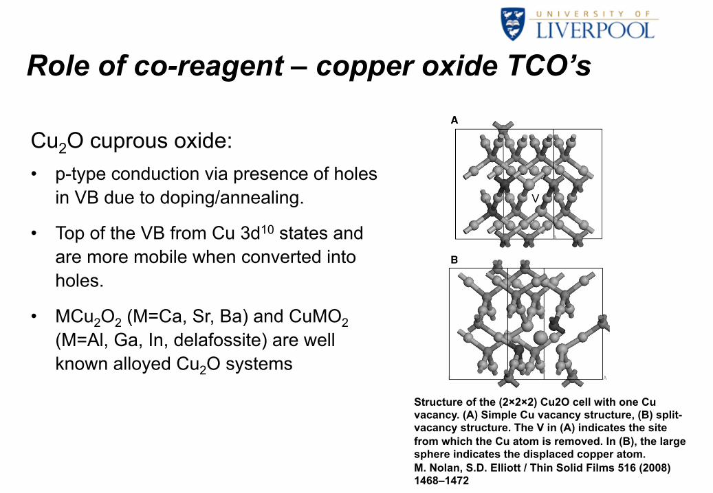
Cu2O cuprous oxide: • p-type conduction via presence of holes
in VB due to doping/annealing.
• Top of the VB from Cu 3d10 states and are more mobile when converted into holes.
• MCu2O2 (M=Ca, Sr, Ba) and CuMO2 (M=Al, Ga, In, delafossite) are well known alloyed Cu2O systems
Role of co-reagent – copper oxide TCO’s
Structure of the (2×2×2) Cu2O cell with one Cu vacancy. (A) Simple Cu vacancy structure, (B) split-vacancy structure. The V in (A) indicates the site from which the Cu atom is removed. In (B), the large sphere indicates the displaced copper atom. M. Nolan, S.D. Elliott / Thin Solid Films 516 (2008) 1468–1472

CpCutBuCN - characteristics
Log10P(mTorr) = -4772.5/T(Kelvin) + 15.863 100°C, giving a vapour pressure of 1.183T
Ref: S. L. Hindley, PhD Thesis, Liverpool, 2013.
cyclopentadienyl copper tertiarybutyl isocyanide,
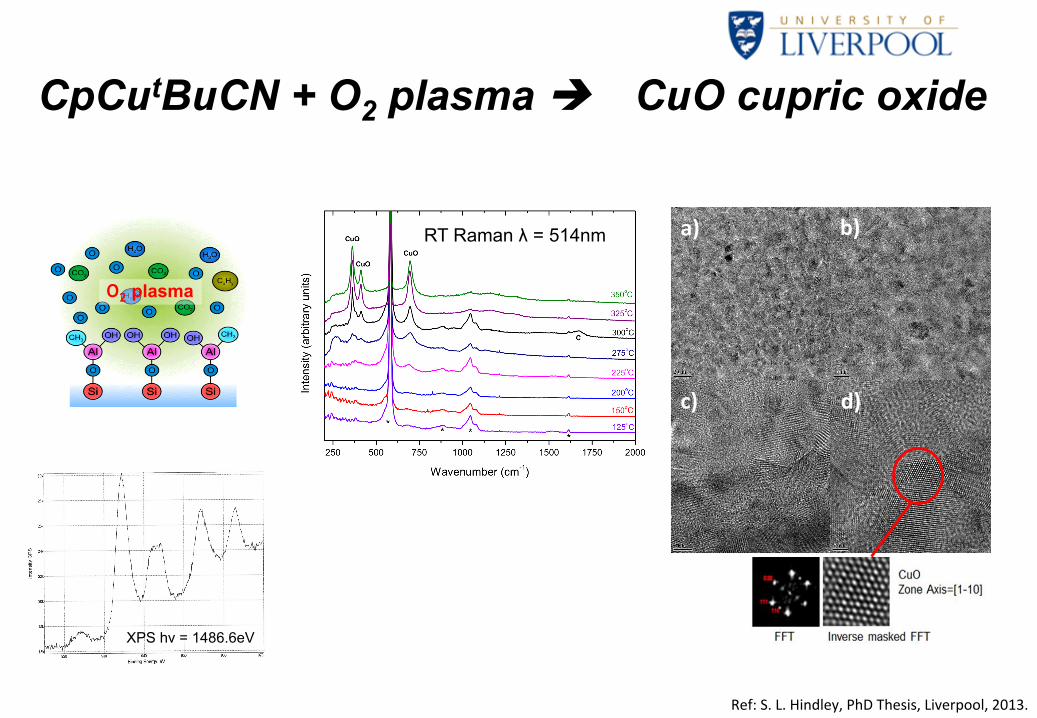
CpCutBuCN + O2 plasma è CuO cupric oxide
a) b)
c) d)
O2 plasma
RT Raman λ = 514nm
XPS hν = 1486.6eV
Ref: S. L. Hindley, PhD Thesis, Liverpool, 2013.

CpCutBuCN + H2O è Cu2O cuprous oxide H2O pulse
Ref: S. L. Hindley, PhD Thesis, Liverpool, 2013.
15
Summary – role of co-reagent
• Choice of co-reagent is not arbitrary
• Water, ozone, O2 plasma play a role in surface chemistry
• Co-reagent influences growth temperature (enthalpy of reaction)
• Other co-reagent can produce metal (H2, plasma), nitride (N2/H2 plasma , NH3, hydrazine) or carbide etc.
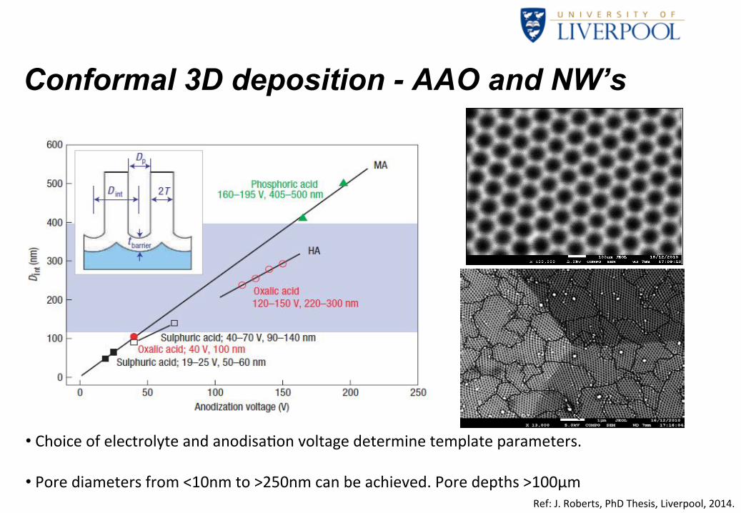
Conformal 3D deposition - AAO and NW’s
• Choice of electrolyte and anodisa-on voltage determine template parameters. • Pore diameters from <10nm to >250nm can be achieved. Pore depths >100μm
Ref: J. Roberts, PhD Thesis, Liverpool, 2014.
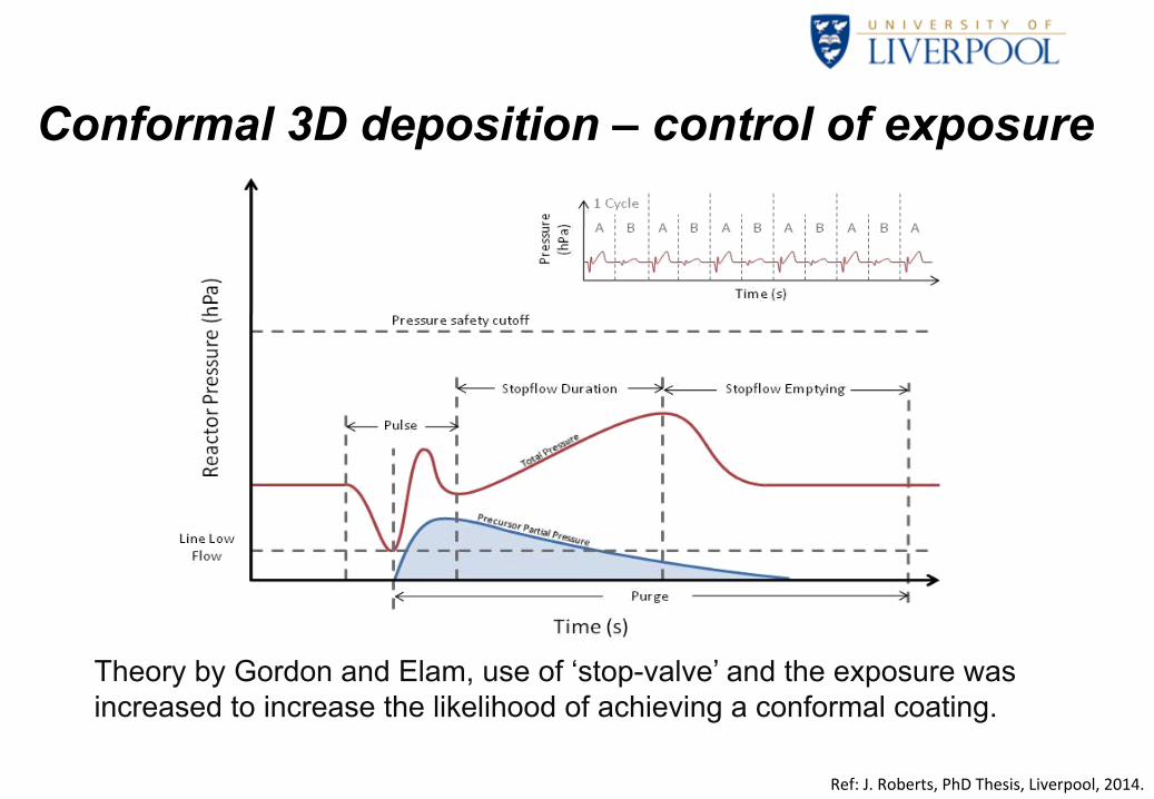
Theory by Gordon and Elam, use of ‘stop-valve’ and the exposure was increased to increase the likelihood of achieving a conformal coating.
Conformal 3D deposition – control of exposure
Ref: J. Roberts, PhD Thesis, Liverpool, 2014.
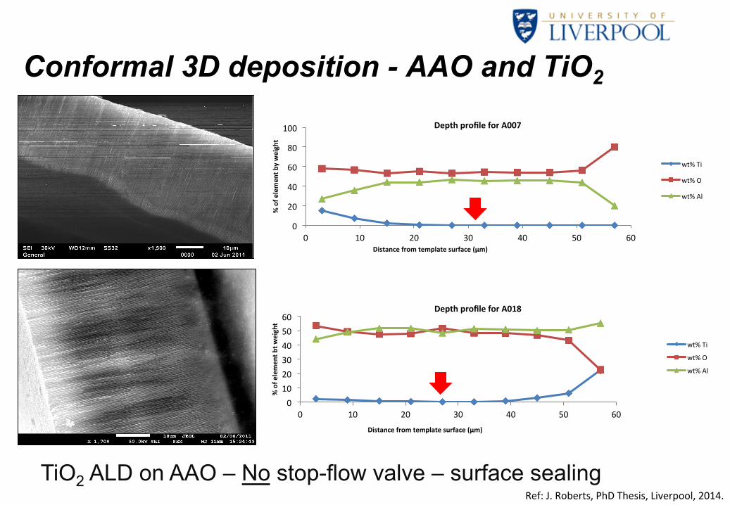
TiO2 ALD on AAO – No stop-flow valve – surface sealing
0
20
40
60
80
100
0 10 20 30 40 50 60
% of e
lemen
t by weight
Distance from template surface (μm)
Depth profile for A007
wt% Ti
wt% O
wt% Al
0 10 20 30 40 50 60
0 10 20 30 40 50 60
% of e
lemen
t bt w
eight
Distance from template surface (μm)
Depth profile for A018
wt% Ti
wt% O
wt% Al
3s Ti dose, 5s Ti hold, 4s Ti purge, 0.05s H2O draw, 1s H2O hold, 10s H2O purge, 300 cycles
Conformal 3D deposition - AAO and TiO2
Ref: J. Roberts, PhD Thesis, Liverpool, 2014.
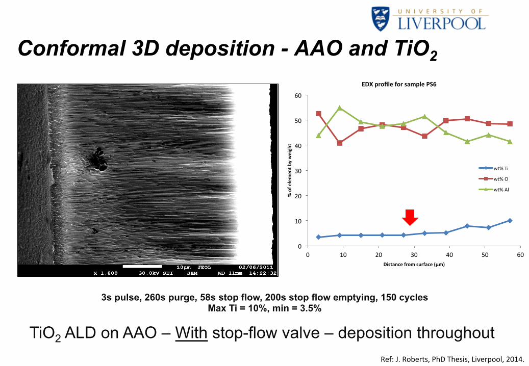
3s pulse, 260s purge, 58s stop flow, 200s stop flow emptying, 150 cycles Max Ti = 10%, min = 3.5%
0
10
20
30
40
50
60
0 10 20 30 40 50 60
% of e
lemen
t by weight
Distance from surface (μm)
EDX profile for sample PS6
wt% Ti
wt% O
wt% Al
Conformal 3D deposition - AAO and TiO2
TiO2 ALD on AAO – With stop-flow valve – deposition throughout Ref: J. Roberts, PhD Thesis, Liverpool, 2014.

Experimental & Results: ALD ZnO coating of CuO Nanowires
CuO nanowires grown by oxidation of strained high purity copper metal 150mins in normal atmosphere at 500°C followed by slow cooling
Conformal 3D deposition – CuO NWs
Ref: J. Roberts, PhD Thesis, Liverpool, 2014.
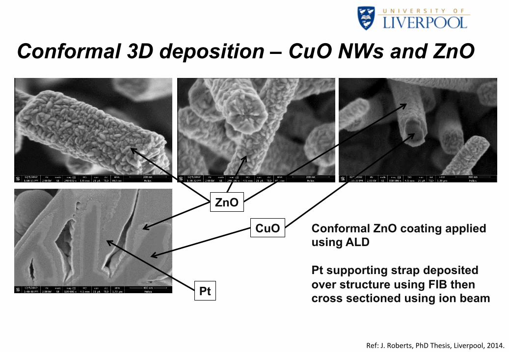
Conformal ZnO coating applied using ALD Pt supporting strap deposited over structure using FIB then cross sectioned using ion beam
ZnO
CuO
Pt
Ref: J. Roberts, PhD Thesis, Liverpool, 2014.
Experimental & Results: Conformal 3D deposition – CuO NWs and ZnO
22
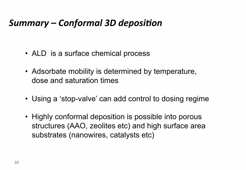
Summary – Conformal 3D deposi5on
• ALD is a surface chemical process
• Adsorbate mobility is determined by temperature, dose and saturation times
• Using a ‘stop-valve’ can add control to dosing regime
• Highly conformal deposition is possible into porous structures (AAO, zeolites etc) and high surface area substrates (nanowires, catalysts etc)

Atomic layer deposition - doping
P1
P2
ALD P1 P2
1st monolayer
2nd monolayer H2O
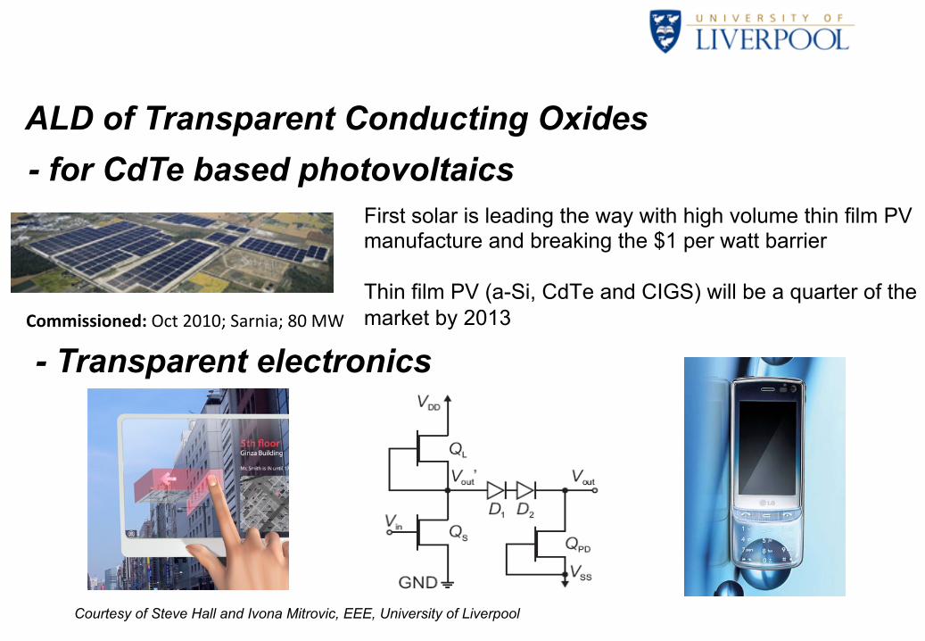
First solar is leading the way with high volume thin film PV manufacture and breaking the $1 per watt barrier Thin film PV (a-Si, CdTe and CIGS) will be a quarter of the market by 2013 Commissioned: Oct 2010; Sarnia; 80 MW
ALD of Transparent Conducting Oxides - for CdTe based photovoltaics
- Transparent electronics
Courtesy of Steve Hall and Ivona Mitrovic, EEE, University of Liverpool

Gallium, germanium and aluminium doped ZnO
0
0.1
0.2
0.3
0.4
0.5
0.6
0.7
0.8
0 50 100 150 200 250 300 350
Temperature (˚C)
Gro
wth
rate
(nm
per
cyc
le)
DEZn
DEZn Diethyl zinc
TMA
TMA Trimethyl aluminium
TEGa TEGa Triethyl gallium GEME
GEME Tetramethoxy germanium
Co-reagent H2O
• No growth of Ga2O3 or GeO2 with TEGa or GEME
• BUT they can be incorporated as dopants in ZnO

Dopant incorporation rates
[Al]
[Ga]
[Ge]
0 2 4 6 8 10 12 14 16 18 20 0
5
10
15
20 D
opan
t ALD
cyc
le fr
actio
n (%
)
Dopant / (Dopant + Zn) content in film (%)
• The proportion of [dopant], measured by EDX spectroscopy is proportional to the dopant precursor ALD cycle fraction.
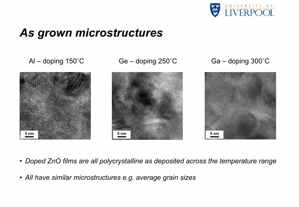
As grown microstructures
Ga – doping 300˚C Al – doping 150˚C Ge – doping 250˚C
5 nm 5 nm 5 nm
• Doped ZnO films are all polycrystalline as deposited across the temperature range
• All have similar microstructures e.g. average grain sizes

Sheet resistance versus doping fraction
• Minimum sheet resistance between 4 – 6% [dopant] incorporation
• Gallium doping produces lowest sheet resistances
106
105
104
103
102
Dopant ALD cycle fraction (dopant / (dopant + DEZn), %)
[Al] [Ge] [Ga]
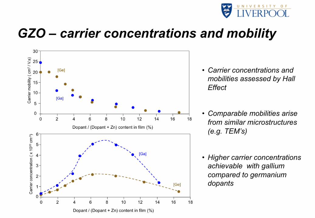
GZO – carrier concentrations and mobility
• Carrier concentrations and mobilities assessed by Hall Effect
• Comparable mobilities arise from similar microstructures (e.g. TEM’s)
• Higher carrier concentrations achievable with gallium compared to germanium dopants

0 500 1000 1500 2000 2500 Wavelength (nm)
100
80
60
40
20
0
Tran
smis
sion
(%)
Ga:ZnO – optical properties
• IR ‘cut-off’ extended by reducing carrier the concentration
• Potential trade-off between thermal management and electrical conductivity
• High performance optical properties
6.9 x 10²⁰
8.4 x 10²⁰
9.4 x 10²⁰
Reflectivity
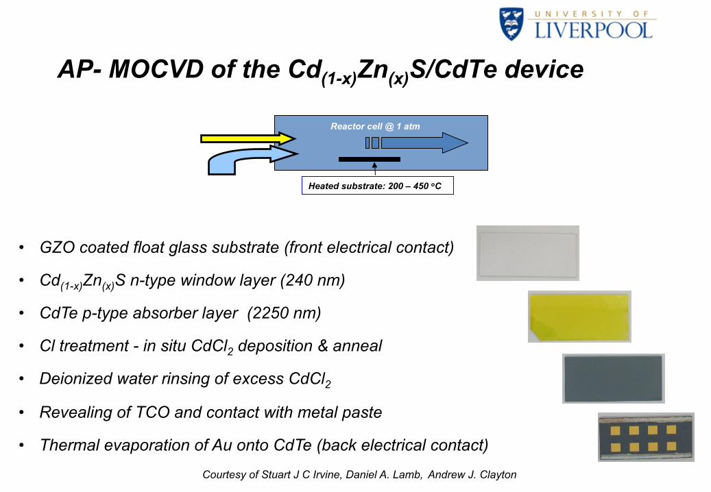
AP- MOCVD of the Cd(1-x)Zn(x)S/CdTe device
• GZO coated float glass substrate (front electrical contact)
• Cd(1-x)Zn(x)S n-type window layer (240 nm)
• CdTe p-type absorber layer (2250 nm)
• Cl treatment - in situ CdCl2 deposition & anneal • Deionized water rinsing of excess CdCl2 • Revealing of TCO and contact with metal paste
• Thermal evaporation of Au onto CdTe (back electrical contact)
Heated substrate: 200 – 450 oC
Reactor cell @ 1 atm H2
Metal-organic precursors
Courtesy of Stuart J C Irvine, Daniel A. Lamb, Andrew J. Clayton
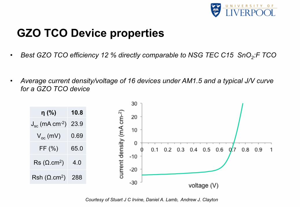
GZO TCO Device properties
η (%) 10.8
Jsc (mA cm-2) 23.9
Voc (mV) 0.69
FF (%) 65.0
Rs (Ω.cm2) 4.0
Rsh (Ω.cm2) 288
• Best GZO TCO efficiency 12 % directly comparable to NSG TEC C15 SnO2:F TCO
• Average current density/voltage of 16 devices under AM1.5 and a typical J/V curve for a GZO TCO device
Courtesy of Stuart J C Irvine, Daniel A. Lamb, Andrew J. Clayton
Summary of doping
33
• Al, Ge and Ga doped – ZnO TCO’s are achievable with ALD doping cycle approach
• Ga-doped ZnO has superior electrical properties to the Al- and Ge-doped ZnO
• ALD TCO’s have ‘comparable’ performance to SnO2:F materials
• Scope to tailor the ZnO – based TCO’s for PV and energy-saving glass applications
Acknowledgements: Funding through U.K. Technology Strategy Board under project TP11/LIB/6/I/AM092J.
Conclusions
34
• ALD can be used to deposit material with atomic scale precision uniformly over 3D structures
• Complex compositions are achievable
• Dielectrics, transparent conductors and metallic materials are feasible
• Application areas span IT, power devices, renewable energy (and others e.g. optics, displays, energy storage, catalysts etc.)

Acknowledgements
Dr Helen Aspinall
Dr Kate Black
Dr Ziwen Fang
Dr Jeff Gaskell
Professor Tony Jones
Dr Peter King
Dr Paul Marshall
Dr Richard Potter
Dr Joe Roberts
Dr Simon Romani
Dr Sarah Hindly
Dr Matt Werner
Dr Jacqueline Wrench


![DESIGN AND APPLICATION OF TRANSPARENT AND TRANSLUCENT … · opaque, translucent, semi-, or totally transparent enamels to be obtained [12]. Lastly, adding refractory oxides, such](https://img.dokumen.tips/doc/110x75/5f1dcd5b47340e360101c359/design-and-application-of-transparent-and-translucent-opaque-translucent-semi-.jpg)