Embed Size (px)
Citation preview

ASIC Back-End Design
Lecture given by Saadat Khan, BAE Systems
Slides prepared by Jamie Bernard, BAE Systems

Agenda
• Introduction• Design Flow
– Overview
– Floorplan
– Timing Driven Placement
– Clock Tree Synthesis
– Routing
• Verification• Design Example

IntroductionIntroduction

Introduction
• Technological Advances– 19th Century - Steel– 20th Century – Silicon
• Growth in Microelectronic (Silicon) Technology– Moore’s Law (# of transistors double/18 months)– One Transistor– Small Scale Integration (SSI)
• Multiple Devices (Transistor / Resistor / Diodes)• Possibility to create more than one logic gate (Inverter, etc)
– Large Scale Integration (LSI)• Systems with at least 1000 logic gates (Several thousand transistors)
– Very Large Scale Integration• Millions to hundreds of millions of transistors (Microprocessors)
– Intel indicates that dual core processors will soon exist that contain 1 billion transistors

Introduction
• Manual (Human) design can occur with small number of transistors
• As number of transistors increase through SSI and VLSI, the amount of evaluation and decision making would become overwhelming (Trade-offs)
– Maintaining performance requirements (Power / Speed / Area)– Design and implementation times become impractical
• How does one create a complex electronic design consisting of millions of transistors?
Automate the Process using Computer-Aided Design (CAD) Tools Automate the Process using Computer-Aided Design (CAD) Tools

Introduction
• CAD tools provide several advantages– Ability to evaluate complex conditions in which solving one
problem creates other problems– Use analytical methods to assess the cost of a decision– Use synthesis methods to help provide a solution – Allows the process of proposing and analyzing solutions to occur
at the same time
• Electronic Design Automation– Using CAD tools to create complex electronic designs (ECAD)– Several companies who specialize in EDA
• Cadence® Design Systems• Magma® Design Automation Inc.• Synopsys®
CAD Tools Allow Large Problems to be SolvedCAD Tools Allow Large Problems to be Solved

Design FlowDesign Flow

Design Flow - Overview
• Generic VLSI Design Flow from System Specification to Fabrication and Testing
• Steps prior to Circuit/Physical design are part of the FRONT-END flow
• Physical Level Design is part of the BACK-END flow
– Physical Design is also known as “Place and Route”
• CAD tools are involved in all stages of VLSI design flow
– Different tools can be used at different stages due to EDA common data formats*
• Synopsys® CAD tool for Physical Design is called Astro™
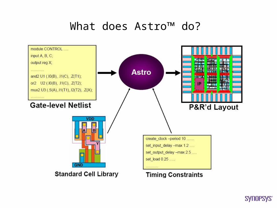
What does Astro™ do?

Where does the Gate Level Netlist come from?1st Input to Astro™

Standard Cell Library2nd Input to Astro™
• Pre-designed collection of logic functions
– OR, AND, XOR, etc
• Contains both Layout and Abstract views
– Layout (CEL) contains drawn mask layers required for fabrication
– Abstract (FRAM) contains only minimal data needed for Astro™
– Timing information• Cell Delay / Pin Capacitance
• Common height for placement purposes

• Integrated circuits are built out of active and passive components, also called devices:
– Active devices• Transistors
• Diodes– Passive devices
• Resistors
• Capacitors• Devices are connected together with polysilicon or metal interconnect:
– Interconnect can add unwanted or parasitic capacitance, resistance and inductance effects
• Device types and sizes are process or technology specific:– The focus here is on CMOS technology
Basic Devices and Interconnect
38

Transistor or Device Representation
Gates are made up of active devices or transistors.Gates are made up of active devices or transistors.
CMOS Inverter Example
OUTIN
Gate Schematic
IN OUT
PMOS
NMOS
Transistor or Device View
VDD
GND
37

What is “Physical Layout”?
Physical Layout – Topography of devices and interconnects, made up of polygons that represent different layers of material.
CMOS Inverter Example
NMOS
PMOS
OUT
VDD
GNDPhysical or Layout View
ININ OUT
PMOS
NMOS
Transistor or Device View
VDD
GND
39

Layout or Mask (aerial) view
Silicon Substrate
Process of Device Fabrication
• Devices are fabricated vertically on a silicon substrate wafer by layering different materials in specific locations and shapes on top of each other
• Each of many process masks defines the shapes and locations of a specific layer of material (diffusion, polysilicon, metal, contact, etc)
• Mask shapes, derived from the layout view, are transformed to silicon via photolithographic and chemical processes
Wafer (cross-sectional) view40

Wafer Representation of Layout Polygons
Example of complimentary devices in 0.25 um CMOS technology or process.
Input
VDD
GND
Output
PMOS
NMOS
0.25 um
Aerial or Layout View Wafer Cross-sectional View
41
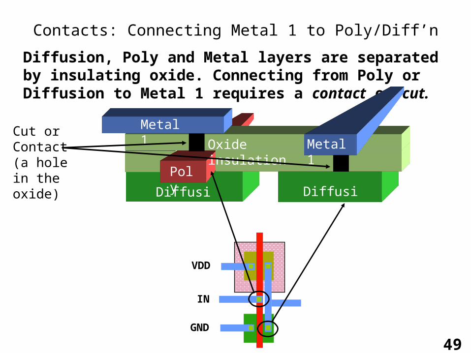
Contacts: Connecting Metal 1 to Poly/Diff’n
Diffusion, Poly and Metal layers are separated by insulating oxide. Connecting from Poly or Diffusion to Metal 1 requires a contact or cut.
Cut or Contact (a hole in the oxide)
VDD
IN
GND
Diffusion Diffusion
Poly
Oxide insulation Metal 1
Metal 1
49

What is meant by “0.xx um Technology”?
- In CMOS Technology the um or nm dimension refers to the channel length, a minimum dimension which is fixed for most devices in the same library.
- Current flow or drive strength of the device is proportional to W/L; Device size or area is proportional to W x L.
Gate or Channel Dimensions (L and W)
Narrower
Width
=
Lower current throug
h channe
l
Length
Width
GATE
W
L
L
Width (W)
Wider Width
=
Higher current throug
h channe
l
GATE
Length
42

Comparing Technologies
The drive strength of both devices is the same: W/L = 6.
The diffusion area (5xLxW) of A is 4x that of B. Which is preferred?
A: 0.5 um Technology
L = 0.5 um
2L 2L
W = 3 um
L = 0.25 um
W = 1.5 um
2L 2L
B: 0.25 um Technology Area Comparison
43

Relative Device Drive Strengths
To double the drive strength of a device, double the channel width (W), or connect two 1X devices in parallel. The latter approach keeps the height at a fixed or “standard” height.
“1X” NMOS (W/L = 6)
GND
OUT
L = 0.25 um
W = 1.5 um
IN
0.25 um
GND
3 um OUT
IN
“2X” NMOS (W/L = 12)
1.5 um
GND
0.25 um
OUT
IN
“2X” NMOS (W/L = 6 + 6)
44

Input Output
Gate Drive Strength Example
PMOS transistor
1x
NMOS transistor
Input Output
Parallel PMOS transistors
2x
inv1 inv2
Parallel NMOS transistors
Each gate in the library is represented by multiple cells with different drive strengths for effective speed vs. area optimization.
45

Drive/Buffering Rules: Max Transition/Cap
1x 2x 1x
1x
1x
Maximum Transition Rule Violation
Maximum Transition Rule Met
Upsized Driver or Added Buffers
Afte
r O
ptim
izat
ion
Bef
ore
Opt
imiz
atio
n
46

Timing Constraints3rd Input to Astro™
• Derived from system specifications and implementation of design
• Identical to timing constraints used during logic synthesis
• Common constraints in electronic designs– Clock Speed/Frequency– Input / Output Delays associated with I/O signals– Multicycle Paths– False Paths
• Astro™ uses these constraints to consider timing during each stage of the place and route process

Concept of Place and Route
• Location of all standard cells is automatically chosen by the tool during placement (Based upon routing and timing)
• Pins are physically connected during routing (Based upon timing)

Concepts of Placement
• Standard cells are placed in “placement rows”
• Cells in a timing-critical path are placed close together to reduce routing related delays (Timing Driven)
• Placement rows can be abutting or non-abutting
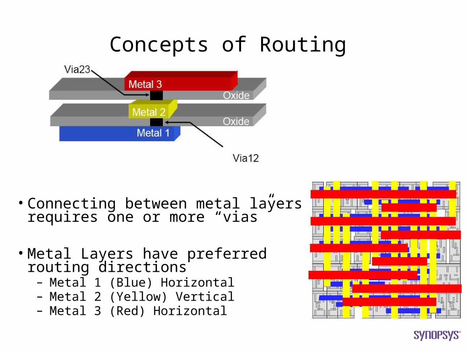
Concepts of Routing
• Connecting between metal layers requires one or more “vias”
• Metal Layers have preferred routing directions
– Metal 1 (Blue) Horizontal– Metal 2 (Yellow) Vertical– Metal 3 (Red) Horizontal

FloorplanFloorplan

Design Flow – Floorplan
• Layout design done at the chip level– Defining layout hierarchy– Estimation of required design area
• A blueprint showing the placement of major components in the design (non-standard cell)
– Inputs / Output (I/O)– RAMs / ROMs/– Reusable Intellectual Property (IP) macros
• Approaches to Floorplanning (Automatic or Manual)– Constructive– Iterative– Knowledge-Based

Design Must Be Floorplanned Before P&R
• Floorplan of design:– Core area defined with large macros placed– Periphery area defined with I/O macros placed– Power and Ground Grid (Rings and Straps) established
• Utilization:– The percentage of the core that is used by placed standard cells and
macros– Goal of 100%, typically 80-85%

I/O Placement and Chip Package Requirements
• Some Bond Wire requirements:
– No Crossing
– Minimum Spacing
– Maximum Angle
– Maximum Length
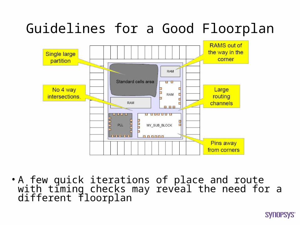
Guidelines for a Good Floorplan
• A few quick iterations of place and route with timing checks may reveal the need for a different floorplan

Defining the Power/Ground Grid and Blockages
• Purpose of Grid is to take the VDD and VSS received from the I/O area and distribute it over the core area
• Blockages can also be added in the floorplan to prohibit standards cells from being placed in those areas

Timing Driven PlacementTiming Driven Placement

Design Flow – Timing Driven Placement
• Astro™ optimizes, places, and routes the logic gates to meet all timing constraints
• Balancing design requirements– Timing– Area– Power– Signal Integrity

Timing Constraints
• Astro™ needs constraints to understand the timing intentions
– Arrival time of inputs– Required arrival time at outputs– Clock period
• Constraints come from the Logic Synthesis tool
– SDC (Synopsys Design Constraints) format

Cell and Net Delays
• Astro™ calculates delay for every cell and every net
• To calculate delays, Astro™ needs to know the resistance and capacitance of each net
– Uses geometry of net and Look Up Tables to estimate the resistances and capacitances

Timing Driven Placement
• Timing Driven Placement places critical path cells close together to reduce net RC
• Prior to routing, RC are based on Virtual Routes
• What if critical paths do not meet timing constraints with placement?

Logic Optimizations
• These optimizations can be done during pre-place, in-place, or post-place stages of placement
• Each optimization can be done separately or all done concurrently during placement (none – one – all)

Clock Tree SynthesisClock Tree Synthesis

Design Flow – Clock Tree Synthesis
• All clock pins are driven by a single clock source
• Large delay and transition time due to length of net
• Clock signal reach some registers before others (Skew)

Clock Tree Topologies
• Clock source is connected to center of the network
• Networks are distributed in a H or X shape until clock pin of register is driven by a local buffer
H-Tree and X-Tree Topologies Solve Single Clock Pin ProblemH-Tree and X-Tree Topologies Solve Single Clock Pin Problem

After Clock Tree Synthesis
• A clock (buffer) tree is built to balance the output loads and minimize the clock skew
• A delay line can be added to the network to meet the minimum insertion delay (clock balancing)

Gated - CTS
• Clocks may not be generated directly from I/O
• Power saving techniques such as clock-gating are used to turn of the clock to sections of the design
• Astro™ can interpret gated clocks and can build clock trees “through” the logic to the registers

Effects of CTS
• Several (Hundreds/Thousands) of clock buffers added to the design
• Placement / Routing congestion may increase
• Non-clock cells may have been moved to less ideal locations
• Timing violations can be introduced

RoutingRouting

Process of Routing Can Be Timing DrivenProcess of Routing Can Be Timing Driven
Design Flow – Routing
• Routing is a fundamental step in the place and route process
• Create metal shapes that meet the requirements of a fabrication process
– The physical connection between cells in the design
• Virtual routes used during placement and CTS need to become reality
– Timing of design needs to be preserved– Timing data such as signal transitions and clock skew needs to
match the virtual route estimates
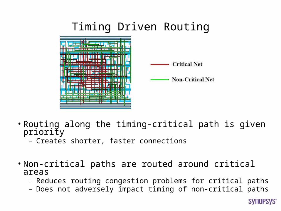
Timing Driven Routing
• Routing along the timing-critical path is given priority– Creates shorter, faster connections
• Non-critical paths are routed around critical areas– Reduces routing congestion problems for critical paths– Does not adversely impact timing of non-critical paths

Concept of Routing Tracks
• Metal routes must meet minimum width and spacing “design rules” to prevent open and short circuits during fabrication
• In grid based routing systems, these design rules determine the minimum center-to-center distance for each metal layer (Track/Grid spacing)
• Congestion occurs if there are more wires to be routed than available tracks

Grid-Based Routing System
• Metal traces (routes) are built along and centered around routing tracks
• Each metal layer has its own tracks and preferred routing direction
– Metal 1 – Horizontal– Metal 2 – Vertical
• Track and pitch information can be located in the technology file
– Design Rules

VerificationVerification

What Happens After Place and Route?
Verification

Formal Verification
• New standard cells have been added to the design through timing optimizations and clock tree synthesis
• The final netlist created by Astro™ needs to be compared to the original gate-level netlist
• Formal verification ensures the functional equivalency at the logic level between the two implementations (original vs. final) of the design
– The intended function was maintained throughout the physical design process
Formality® is the Sign-Off Tool for Formal VerificationFormality® is the Sign-Off Tool for Formal Verification

Timing Verification• Star-RCXT™ performs the layout parasitic extraction of
the resistances and capacitances of all routes in the design
• Results in a format such as SPEF (Standard Parasitic Extended Format)
– SPEF is an smaller, extended format of Standard Parasitic Format (SPF), which enables the transfer of design specific resistances and capacitances from physical design to timing analysis and simulation tools
• Primetime® performs static timing analysis– Detects timing violations by combining SPEF from Star-RCXT™
and netlist from Astro™ and checks against the design timing constraints (clock frequencies)
Star-RCXT™ and Primetime® are the Sign-Off Tools for Timing Verification
Star-RCXT™ and Primetime® are the Sign-Off Tools for Timing Verification

Physical Verification• Checks the design for fabrication feasibility and physical
defects that could result in the design to not function properly
– 3 checks (DRC, ERC, and LVS)
• Design Rule Checks (DRC)– Verifies that design does not violate any fabrication rules
associated with the target process technology (metal width/space, antenna ratio, etc)
• Electrical Rules Checks (ERC)– Verifies that there are no short or open circuits with power and
ground as well as resistors/capacitors/transistors with floating nodes (part of LVS)
• Layout Versus Schematic (LVS)– Final physical design matches the logical (schematic) version in
terms of correct connectivity and number of electrical devices
Hercules™ is the Sign-Off Tool for Physical VerificationHercules™ is the Sign-Off Tool for Physical Verification

Fabrication
• Physical Design process is complete upon successful completion of timing, functional, and physical verification
• The design can be “Taped-Out” and GDSII created for the manufacturer
– GDSII (Graphic Design System II) is a binary format containing the physical geometry information of the design.
– The shapes are assigned numeric attributes in the form of “Layer Number” and “Data Type” (Metal 1 => 100:0)
• Fabrication and Test determine which chips can be implemented into the system (yield)

Physical designData
GDSII (Stream)
Masks
Wafer
Mask Generation – GDSII / Stream
30
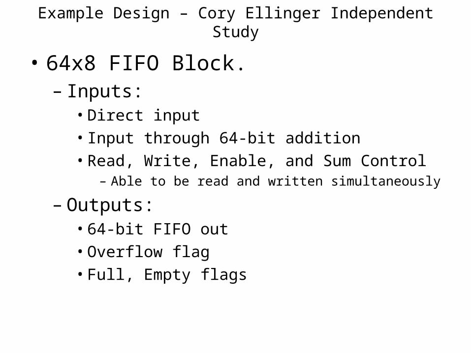
Example Design – Cory Ellinger Independent Study
• 64x8 FIFO Block.– Inputs:
• Direct input• Input through 64-bit addition• Read, Write, Enable, and Sum Control
– Able to be read and written simultaneously
– Outputs:• 64-bit FIFO out• Overflow flag• Full, Empty flags

Block Diagram
register register
unsignedAdder
register bank
clkrst
add_fifo
sum_cnt
64 x 8 FIFO
rdwren
fullempty
overfl
6464
64
64
data_in_x data_in_y_fifo_in
data_out

Block Diagram – Critical Path
register register
unsignedAdder
register bank
clkrst
add_fifo
sum_cnt
64 x 8 FIFO
rdwren
fullempty
overfl
6464
64
64
data_in_x data_in_y_fifo_in
data_out
Critical Path
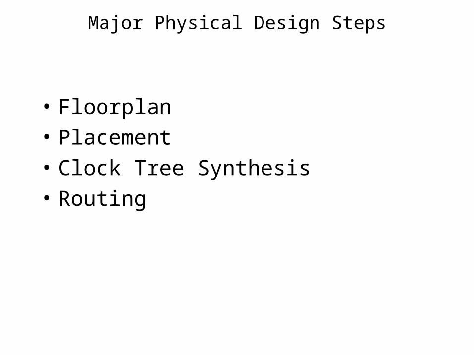
Major Physical Design Steps
• Floorplan
• Placement
• Clock Tree Synthesis
• Routing
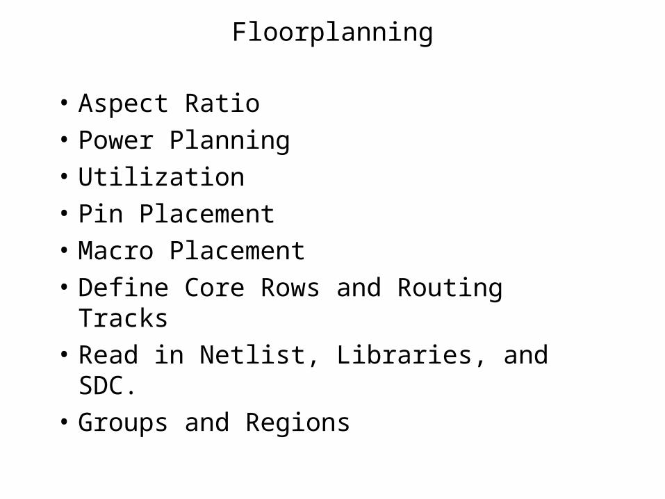
Floorplanning
• Aspect Ratio
• Power Planning
• Utilization
• Pin Placement
• Macro Placement
• Define Core Rows and Routing Tracks
• Read in Netlist, Libraries, and SDC.
• Groups and Regions

Floorplan (Theoretical)
Aspect Ratio (2:1) W:H
FIFO
Input Register
Data Flow
64
da
ta_
in
data out
output flags
64
da
ta_
in
sum_cnt clk reset

Floorplan
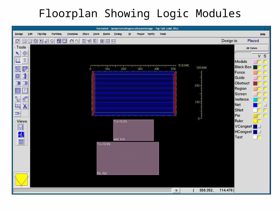
Floorplan Showing Logic Modules
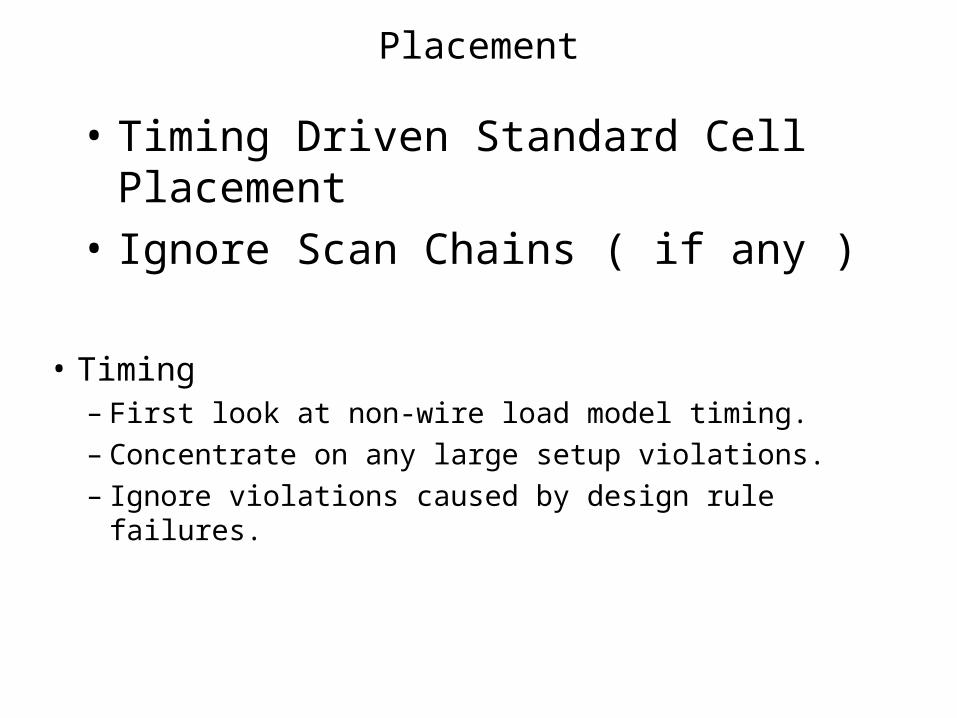
Placement
• Timing Driven Standard Cell Placement
• Ignore Scan Chains ( if any )
• Timing– First look at non-wire load model timing.– Concentrate on any large setup violations.– Ignore violations caused by design rule
failures.

AutoPlace of Logic Modules

Design Placement

Reset Net
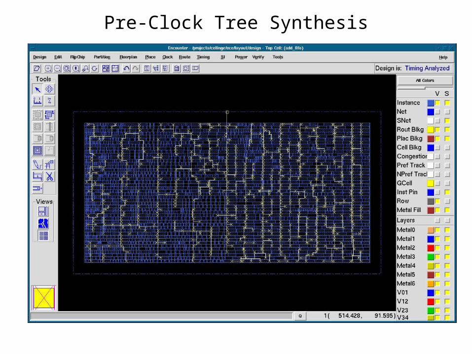
Pre-Clock Tree Synthesis

Clock Tree Synthesis
• Goals:– Low Clock Skew– Low Clock Insertion Delay– Sharp Transitions
• Timing– Setup violations clean– Design Rules fixed– Initial evaluation of real hold violations

Post Clock Tree Synthesis

Routed Design

Route (zoom)

QUESTIONS ?QUESTIONS ?