Embed Size (px)
Citation preview

Rational Design of Zinc Phosphide
Heterojunction Photovoltaics
Thesis byJeffrey Paul Bosco
In Partial Fulfillment of the Requirementsfor the Degree of
Doctor of Philosophy
California Institute of TechnologyPasadena, California
2014
(Defended May 30, 2014)

ii

© 2014
Jeffrey Paul Bosco
All Rights Reserved
i

ii

“Look here, I have succeeded at last in fetching some gold from the sun.”
– Gustav Kirchhoff
(After his banker questioned the value of investigating gold in the Fraunhofer
lines of the sun and Kirchhoff handing him over a medal he was awarded for
his investigations.)
iii

iv

Acknowledgements
First and foremost I would like to thank my research advisor, Prof. Harry
Atwater, for the tremendous amount of support he has provided during my
tenure at Caltech. I first met Harry during a chemical engineering recruiting
trip. He handed me a copy of Scientific American, blasted me with energy and
excitement over the future of plasmonics (of course I had never even heard of a
surface plasmon at that point), and rushed off! Little did I know that I would
be working in the Atwater labs only six months later and Harry would meet
me with the same energy and enthusiasm regarding the topic of zinc phosphide
photovoltaics. Five years later and he is still an incredible source of support,
advice, and interesting scientific ideas. Thank you Harry.
I am also indebted to the members of my thesis committee, Prof. Nathan
Lewis, Prof. Kostantinos Giapis, and Prof. Richard Flagan. In particular,
Nate has been an excellent scientific resource over the past couple of years. I
clearly remember handing Nate a draft of my first (and in my eyes perfectly
rigorous) scientific manuscript, only to have it returned a week later, so thor-
oughly plastered with corrections written in red ink that it looked like someone
had literally ripped an artery right out of the paper. Lesson learned and my
next manuscript draft came back from Nate with only a couple of scratches.
It is common that one’s thesis work is built upon the previous discoveries
of others. Dr. Greg Kimball initially started the zinc phosphide solar project
and the knowledge he contributed to the field of earth-abundant photovoltaics
has been indispensable to my work. Greg also made a great mentor, laboratory
accomplice, and friend. I worked alongside of several other individuals on the
Zn3P2 project, including Dr. Seokmin Jeon (Seokmin’s STM work is featured
in Chapter 3), Faisal Tajdar, and Andrew Gong. Some of this work depended
heavily on the theoretical calculations made by Dr. Steve Demers and Prof.
David Scanlon. David not only made a productive theoretical collaborator,
but also a great late-night drinking partner at various conferences. Finally,
v

Dr. Steve Rozeveld of The DOW Chemical Company provided countless TEM
images (and presumably countless hours of his time) of epitaxial Zn3P2 films
for which I have received many compliments on their stunning clarity. Zn3P2
is also not the only “earth-abundant” solar material that the Atwater group
studies, and therefore I have not been the only person burdened with the
challenge of working with an unstudied semiconductor. I am thankful to have
worked alongside of Samantha Wilson, Naomi Coronel, Yulia Tolstova, and
Amanda Shing, who have shared many of the same trials and tribulations
(and inevitable headaches) regarding the material science and device physics
of novel materials.
There are a number of individuals in charge of the instruments that I used
heavily during my thesis work. I know that training for and maintenance
of any piece of scientific equipment is a completely thankless task. There-
fore, I would like to directly acknowledge the following for their extreme pa-
tience and commitment: Joseph Beardsley (Kratos XPS), Emily Warmman
(HRXRD), Bruce Brunswig (MMRC), Ryan Briggs and Stan Berkos (ellip-
someter), Carissa Eisler (sputterer), John Lloyd, Cris Flowers, and Rob Cor-
ridan (e-beam evaporators), Michael Deceglie, Michael Kelzenberg (solar sim-
ulator), Hal Emmer and Chris Chen (various laboratory responsibilities). I
owe a special thanks to Lise Lahourcade, who caused an abrupt increase in
my productivity when she taught me how to use a RHEED gun as well as Ma-
rina Leite for introducing me to single-crystal x-ray diffraction. Of course, a
laboratory functions beyond the efforts of any one individual and I owe many
thanks to the collaborative nature of the entire Atwater and Lewis groups.
Without their ideas and support, this thesis would not have been possible.
The funding for my thesis project came from two distinct sources: the NSF
graduate research fellowship and the DOW Chemical Company. I had a num-
ber of fruitful interactions with members of The DOW Chemical Company’s
solar research team. Many thanks to Dr. James Stevens, Dr. Marty DeG-
root, Dr. Rebekah Feist, Dr. Robert Wright, Dr. Melissa Mushrush, and Dr.
vi

Manish Sharma for their professional and scientific mentoring.
The social landscape of graduate school can be a difficult terrain to tra-
verse. I am indebted to a number of individuals who have made the entire PhD
process a rich experience. To my first year Chemical Engineering classmates,
who quickly became a second family as we spent tireless nights in Spalding
Laboratory slaving away at pages of index notation, vehemently arguing about
thermodynamic systems, and imbibing our fair share of margaritas and mind
erasers at Amigos. They helped me survive John Brady’s four hour transport
exams and the notorious ChemE qualifier and somehow made this whole pro-
cess a total a blast! Thanks again, guys (and Amy!). I thank my office mates,
Seyoon Kim and Nick Batara, with whom I had countless conversations about
food, beer, and any number of pointless topics. There is also nothing like es-
caping to Santa Monica on weekend mornings to vent one’s frustrations in an
intense game of doubles beach volleyball. Thanks to Prof. Nick Strandewitz,
Morgan Putnam, Dan Turner-Evans, Rob Usiskin and many others for being
such excellent (well, at least enthusiastic) players. Whether it was camping
in the deserts of Nevada, climbing the rocky switchbacks of Mount Fuji, or
playing a heated game of Risk with too many glasses of wine, Vanessa Heck-
man and Brett Babin were always fantastic partners in crime. And, I owe
many thanks to Mikhail Hanewich-Hollatz, Amanda Jee-young Mock, Luke
Urban, Samantha Wilson, Dan Lin, and Naeem Hussain for being excellent
close friends and maintaining my sanity throughout the last few years.
Finally, the members of my family, Colleen, Paul, and Kate Bosco, have
been incredibly supportive throughout this entire process, despite my uncanny
ability to forget to return telephone calls. And Michelle Lukiman, who has
challenged me in so many ways that even the PhD process has failed to do.
Thank you all.
Jeffrey P. Bosco
May 30th, 2014
Pasadena, CA
vii

viii

Abstract
The prospect of terawatt-scale electricity generation using a photovoltaic (PV)
device places strict requirements on the active semiconductor optoelectronic
properties and elemental abundance. After reviewing the constraints placed on
an “earth-abundant” solar absorber, we find zinc phosphide (α-Zn3P2) to be
an ideal candidate. In addition to its near-optimal direct band gap of 1.5 eV,
high visible-light absorption coefficient (>104 cm−1), and long minority-carrier
diffusion length (>5 µm), Zn3P2 is composed of abundant Zn and P elements
and has excellent physical properties for scalable thin-film deposition. How-
ever, to date, a Zn3P2 device of sufficient efficiency for commercial applications
has not been demonstrated. Record efficiencies of 6.0% for multicrystalline
and 4.3% for thin-film cells have been reported, respectively. Performance has
been limited by the intrinsic p-type conductivity of Zn3P2 which restricts us to
Schottky and heterojunction device designs. Due to our poor understanding
of Zn3P2 interfaces, an ideal heterojunction partner has not yet been found.
The goal of this thesis is to explore the upper limit of solar conversion effi-
ciency achievable with a Zn3P2 absorber through the design of an optimal het-
erojunction PV device. To do so, we investigate three key aspects of material
growth, interface energetics, and device design. First, the growth of Zn3P2 on
GaAs(001) is studied using compound-source molecular-beam epitaxy (MBE).
We successfully demonstrate the pseudomorphic growth of Zn3P2 epilayers of
controlled orientation and optoelectronic properties. Next, the energy-band
alignments of epitaxial Zn3P2 and II-VI and III-V semiconductor interfaces
are measured via high-resolution x-ray photoelectron spectroscopy in order to
determine the most appropriate heterojunction partner. From this work, we
identify ZnSe as a nearly ideal n-type emitter for a Zn3P2 PV device. Finally,
various II-VI/Zn3P2 heterojunction solar cells designs are fabricated, includ-
ing substrate and superstrate architectures, and evaluated based on their solar
conversion efficiency.
ix

x

Contents
Acknowledgements v
Abstract ix
List of Figures xv
List of Tables xix
List of Publications xxi
1 Introduction to earth-abundant photovoltaics 1
1.1 Thin film PV . . . . . . . . . . . . . . . . . . . . . . . . . . . . . . 5
1.1.1 Physics of thin film solar cells . . . . . . . . . . . . . . . . 5
1.1.2 Current thin film PV technologies . . . . . . . . . . . . . 8
1.2 Properties of zinc phosphide (α-Zn3P2) . . . . . . . . . . . . . . 10
1.2.1 Physical properties . . . . . . . . . . . . . . . . . . . . . . 10
1.2.2 Optical properties . . . . . . . . . . . . . . . . . . . . . . . 12
1.2.3 Electronic properties . . . . . . . . . . . . . . . . . . . . . 14
1.2.4 Materials challenges . . . . . . . . . . . . . . . . . . . . . . 15
1.3 Review of prior Zn3P2 photovoltaic device studies . . . . . . . . 16
1.3.1 Mg/Zn3P2 Schottky diodes . . . . . . . . . . . . . . . . . 16
1.3.2 Heterojunction Zn3P2 solar cells . . . . . . . . . . . . . . 18
1.4 Scope of this thesis . . . . . . . . . . . . . . . . . . . . . . . . . . . 19
xi

2 Growth of Zn3P2 by molecular-beam epitaxy 21
2.1 Introduction . . . . . . . . . . . . . . . . . . . . . . . . . . . . . . . 21
2.2 Fundamentals of molecular-beam epitaxy . . . . . . . . . . . . . 24
2.3 Zn3P2 compound source . . . . . . . . . . . . . . . . . . . . . . . . 27
2.3.1 Synthesis of Zn3P2 from the elements . . . . . . . . . . . 27
2.3.2 Zn3P2 compound effusion source . . . . . . . . . . . . . . 29
2.4 Epilayer growth . . . . . . . . . . . . . . . . . . . . . . . . . . . . . 31
2.4.1 Heteroepitaxial substrate . . . . . . . . . . . . . . . . . . . 32
2.4.2 Initial growth results . . . . . . . . . . . . . . . . . . . . . 34
2.4.3 Two-dimensional growth . . . . . . . . . . . . . . . . . . . 37
2.5 Conclusions . . . . . . . . . . . . . . . . . . . . . . . . . . . . . . . 37
3 Ex situ characterization of Zn3P2 epilayers 39
3.1 Growth rate and film morphology . . . . . . . . . . . . . . . . . . 39
3.2 Surface and interface characterization . . . . . . . . . . . . . . . 44
3.3 Optical properties . . . . . . . . . . . . . . . . . . . . . . . . . . . 46
3.4 Electrical properties . . . . . . . . . . . . . . . . . . . . . . . . . . 47
3.4.1 Intrinsic doping . . . . . . . . . . . . . . . . . . . . . . . . 48
3.4.2 Extrinsic p-type doping . . . . . . . . . . . . . . . . . . . 50
3.4.3 Extrinsic n-type doping . . . . . . . . . . . . . . . . . . . 52
3.5 Conclusions . . . . . . . . . . . . . . . . . . . . . . . . . . . . . . . 54
4 Growth and characterization of II-VI materials 57
4.1 Zinc sulfide (ZnS) growth . . . . . . . . . . . . . . . . . . . . . . . 59
4.2 Zinc selenide (ZnSe) growth . . . . . . . . . . . . . . . . . . . . . 64
4.3 Cadmium sulfide (CdS) growth . . . . . . . . . . . . . . . . . . . 66
4.4 Zinc oxide (ZnO) sputter deposition . . . . . . . . . . . . . . . . 67
4.5 Alternative: ZnxMg1-xSySe1-y quaternary alloy . . . . . . . . . . 68
4.6 Conclusions . . . . . . . . . . . . . . . . . . . . . . . . . . . . . . . 69
xii

5 Band energetics of II-VI/Zn3P2 heterostructures 71
5.1 Introduction to energy-band alignments . . . . . . . . . . . . . . 71
5.1.1 Anderson energy-band alignment . . . . . . . . . . . . . . 72
5.1.2 Effective dipole model . . . . . . . . . . . . . . . . . . . . 72
5.1.3 Advanced methods . . . . . . . . . . . . . . . . . . . . . . 76
5.2 Experimental determination of ∆EV and ∆EC . . . . . . . . . . 76
5.2.1 X-ray photoelectron spectroscopy measurement . . . . . 78
5.2.2 DFT determination of the EVBM position . . . . . . . . . 80
5.3 Band alignment results . . . . . . . . . . . . . . . . . . . . . . . . 83
5.3.1 Bulk semiconductor valence-band region . . . . . . . . . 83
5.3.2 ZnS/Zn3P2 band alignment . . . . . . . . . . . . . . . . . 86
5.3.3 ZnSe/Zn3P2 band alignment . . . . . . . . . . . . . . . . . 88
5.3.4 CdS/Zn3P2 band alignment . . . . . . . . . . . . . . . . . 90
5.3.5 ZnO/Zn3P2 band alignment . . . . . . . . . . . . . . . . . 91
5.4 Discussion . . . . . . . . . . . . . . . . . . . . . . . . . . . . . . . . 92
5.4.1 II-VI/Zn3P2 band offsets – measurement vs. prediction 92
5.4.2 Band alignment and photovoltaic device performance . 95
5.5 Conclusions . . . . . . . . . . . . . . . . . . . . . . . . . . . . . . . 97
6 Zn3P2 photovoltaic devices 99
6.1 Substrate devices . . . . . . . . . . . . . . . . . . . . . . . . . . . . 99
6.1.1 ZnS/Zn3P2 heterojunction solar cell . . . . . . . . . . . . 100
6.1.2 ZnSe/Zn3P2 solar cells . . . . . . . . . . . . . . . . . . . . 103
6.2 Superstrate ZnSe devices . . . . . . . . . . . . . . . . . . . . . . . 105
6.2.1 Zn3P2/ZnSe film characterization . . . . . . . . . . . . . . 106
6.2.2 Contact measurements . . . . . . . . . . . . . . . . . . . . 108
6.2.3 Mesa device characterization . . . . . . . . . . . . . . . . 110
6.3 Alternative: Graphene/Zn3P2 Field-effect solar cell . . . . . . . 113
6.4 Conclusions . . . . . . . . . . . . . . . . . . . . . . . . . . . . . . . 115
7 Final remarks 117
xiii

Bibliography 119
Appendix A 137
A.1 Comparison of potential heteroepitaxial templates . . . . . . . . 137
A.2 Eg and χ calculations for ZnxMg1−xSySe1−y quaternary alloys . 137
A.3 Calculated DFT band structures for II-VI semiconductors . . . 139
A.4 X-ray photoionization cross sections for group II, V, and VI
elements . . . . . . . . . . . . . . . . . . . . . . . . . . . . . . . . . 142
A.5 XPS data for II-VI/Zn3P2 heterojunctions . . . . . . . . . . . . . 143
xiv

List of Figures
1.1 Estimated area of installed PV required to meet the current
U.S. total energy and electricity consumption. . . . . . . . . . . 2
1.2 World annual production vs. abundance for elements available
in the Earth’s crust. . . . . . . . . . . . . . . . . . . . . . . . . . . 4
1.3 Schematic diagram and ideal current-voltage characteristics of
a p-n junction photovoltaic device. . . . . . . . . . . . . . . . . . 6
1.4 The Zn–P binary phase diagram and unit cell for the α-Zn3P2
tetragonal crystal structure. . . . . . . . . . . . . . . . . . . . . . 11
1.5 Electronic band structure of α-Zn3P2 calculated by hybrid DFT. 13
1.6 Process flow for the design and optimization of Zn3P2 solar cells. 19
2.1 Schematics of a standard Knudsen effusion cell and the reflec-
tion high-energy electron diffraction (RHEED) measurement. . 25
2.2 Synthesis process and furnace setup for lab-scale production of
phase pure Zn3P2 from the elements. . . . . . . . . . . . . . . . . 28
2.3 Zn3P2 compound source beam pressure and vapor composition. 30
2.4 RHEED images of the GaAs(001) surface after exposure to dif-
ferent surface preparation techniques. . . . . . . . . . . . . . . . 34
2.5 RHEED images of the Zn3P2 growth surface on GaAs(001) un-
der increasing additional Zn flux. . . . . . . . . . . . . . . . . . . 35
2.6 Comparison of RHEED and simulated SAED patterns collected
on three-dimensional Zn3P2 surfaces. . . . . . . . . . . . . . . . . 36
xv

2.7 RHEED images collected on Zn3P2 epilayers grown at varying
substrate temperatures. . . . . . . . . . . . . . . . . . . . . . . . . 38
3.1 Zn3P2 growth rate as a function of substrate temperature. . . . 40
3.2 AFM topography images of Zn3P2 surfaces for films grown at
increasing substrate temperatures. . . . . . . . . . . . . . . . . . 41
3.3 Symmetric HRXRD and rocking curves of Zn3P2 epilayers. . . . 42
3.4 Reciprocal space maps collected on thin Zn3P2 epilayers. . . . . 43
3.5 Transmission electron micrographs of pseudomorphic Zn3P2 lay-
ers with thicknesses of 50 nm and 150 nm . . . . . . . . . . . . . 44
3.6 HR-TEM of the Zn3P2/GaAs interface showing the presence of
a strained GaP layer. . . . . . . . . . . . . . . . . . . . . . . . . . 46
3.7 STM images and the proposed growth mechanism of Zn3P2 on
the Ga-rich GaAs(001) surface. . . . . . . . . . . . . . . . . . . . 47
3.8 Refractive index and extinction coefficient collected on an opti-
cally thick Zn3P2 epilayer. . . . . . . . . . . . . . . . . . . . . . . 48
3.9 Film resistivity and hole density and mobility measured for
Zn3P2 epilayers as a function of thickness. . . . . . . . . . . . . . 49
3.10 RHEED images of Zn3P2 surfaces grown with Ag, Al, and S
impurity incorporation. . . . . . . . . . . . . . . . . . . . . . . . . 51
3.11 Thin-film resistivity and hole mobility of annealed Ag-doped
Zn3P2 epilayers. . . . . . . . . . . . . . . . . . . . . . . . . . . . . . 53
3.12 Symmetric HRXRD of zinc sulfide-phosphide epilayers. . . . . . 55
4.1 RHEED images of ZnS epilayers grown on GaAs(001). . . . . . 60
4.2 High-resolution XRD and TEM of ZnS grown on GaAs(001). . 61
4.3 Hall effect and SIMS measurements of Al-doped ZnS epilayers. 63
4.4 High-resolution XRD of ZnSe epilayers grown on GaAs(001). . 65
4.5 TEM and SAED collected on a 300 nm thick, pseudomorphic
ZnSe film grown on GaAs(001). . . . . . . . . . . . . . . . . . . . 66
xvi

4.6 Van der Pauw resistivity vs. Hall carrier concentration of Al-
doped ZnSe epilayers grown on GaAs(001). . . . . . . . . . . . . 67
4.7 ao, χ, and Eg calculated for a ZnxMg1-xSySe1-y quaternary alloy. 69
5.1 Original Anderson energy-band diagrams for an ideal semicon-
ductor heterojunction. . . . . . . . . . . . . . . . . . . . . . . . . . 73
5.2 Schematic of the heterojunction effective dipole calculation pro-
posed by Ruan and Ching. . . . . . . . . . . . . . . . . . . . . . . 75
5.3 Schematic of the Kraut method for determining ∆EV using pho-
toemission measurements. . . . . . . . . . . . . . . . . . . . . . . . 78
5.4 The Au 4f core level x-ray photoelectron spectrum. . . . . . . . 83
5.5 Comparison x-ray photoelectron spectra and the calculated VB-
DOS for the valence-band region of bulk Zn3P2 . . . . . . . . . . 84
5.6 X-ray photoelectron spectra and DFT calculations for the valence-
band regions of bulk II-VI films. . . . . . . . . . . . . . . . . . . . 85
5.7 XPS survey scans of ZnS/Zn3P2 heterojunction interfaces. . . . 86
5.8 Fitted XPS data and the calculated energy-band diagram of the
ZnS/Zn3P2 heterojunction. . . . . . . . . . . . . . . . . . . . . . . 87
5.9 Fitted XPS data and the calculated energy-band diagram of the
ZnSe/Zn3P2 heterojunction. . . . . . . . . . . . . . . . . . . . . . 89
5.10 Fitted XPS data and the calculated energy-band diagram of the
CdS/Zn3P2 heterojunction. . . . . . . . . . . . . . . . . . . . . . . 90
5.11 Fitted XPS data and the calculated energy-band diagram of the
ZnO/Zn3P2 heterojunction. . . . . . . . . . . . . . . . . . . . . . . 92
5.12 Comparison of predicted and measured II-VI/Zn3P2 heterojunc-
tion band offsets. . . . . . . . . . . . . . . . . . . . . . . . . . . . . 93
6.1 Schematic of a substrate II-VI/Zn3P2 heterojunction solar cell. 100
6.2 Dark and illuminated I-V response of a ZnS/Zn3P2 heterojunc-
tion photovoltaic device. . . . . . . . . . . . . . . . . . . . . . . . 101
6.3 Schematic and I-V response of the Mg/ZnS/Zn3P2 MIS device. 102
xvii

6.4 Dark and illuminated I-V response of a ZnSe/Zn3P2 heterojunc-
tion photovoltaic device. . . . . . . . . . . . . . . . . . . . . . . . 104
6.5 High-resolution TEM and XPS of the untreated ZnSe/Zn3P2
heterojunction interface. . . . . . . . . . . . . . . . . . . . . . . . 105
6.6 Alternative growth strategies for improving the ZnSe emitter. . 106
6.7 High-resolution XRD and TEM of a superstrate Zn3P2/ZnSe
heterojunction interface. . . . . . . . . . . . . . . . . . . . . . . . 107
6.8 Transmission line data and contact resistances for n-GaAs. . . . 109
6.9 Transmission line data and contact resistance for n-ZnSe. . . . 110
6.10 I-V measurements for estimating the contact resistance at n-
ZnSe/n-GaAs interfaces. . . . . . . . . . . . . . . . . . . . . . . . 111
6.11 Schematic of the mesa architecture for a superstrate Zn3P2/ZnSe
photovoltaic device. . . . . . . . . . . . . . . . . . . . . . . . . . . 112
6.12 Dark and illuminated I-V curves of etch-thru and masked Zn3P2/ZnSe
mesa devices. . . . . . . . . . . . . . . . . . . . . . . . . . . . . . . 113
6.13 Cross-sectional schematic of the Field-effect gated graphene/Zn3P2
Schottky device. . . . . . . . . . . . . . . . . . . . . . . . . . . . . 114
6.14 Ideal and measured band diagrams for a graphene/Zn3P2 device
under non-equilibrium, equilibrium, and forward-bias conditions. 115
6.15 Top-view image and I-V data of a graphene/Zn3P2 device under
bias. . . . . . . . . . . . . . . . . . . . . . . . . . . . . . . . . . . . 116
A.1 Thermal expansivity vs. lattice mismatch for a large number of
potential crystalline substrate materials. . . . . . . . . . . . . . . 138
A.2 Band diagrams for Zn3P2 and II-VI compound semiconductors. 140
xviii

List of Tables
1.1 Properties of champion Zn3P2 solar cells. . . . . . . . . . . . . . 17
3.1 Tabulated data of XRD, van der Pauw, and Hall effect mea-
surements. . . . . . . . . . . . . . . . . . . . . . . . . . . . . . . . . 56
5.1 X-ray photoelectron spectroscopy core-level fitting parameters. 81
A.1 Calculated effective mass values (mh/mo) for the first three va-
lence bands of Zn3P2. . . . . . . . . . . . . . . . . . . . . . . . . . 141
A.2 Electronic properties of Zn3P2 used in the dipole calculations. . 141
A.3 X-ray photoionization cross sections of group II, V, and VI el-
ements. . . . . . . . . . . . . . . . . . . . . . . . . . . . . . . . . . . 142
A.4 XPS binding energies for ZnS/Zn3P2 heterointerface samples . 144
A.5 XPS binding energies for ZnSe/Zn3P2 heterointerface samples . 145
A.6 XPS binding energies for CdS/Zn3P2 heterointerface samples . 146
A.7 XPS binding energies for ZnO/Zn3P2 heterointerface samples . 147
xix

xx

List of Publications
The work in this thesis was primarily drawn from the following publications:
J.P. Bosco, S.J. Rozeveld, and H.A. Atwater. “Growth and morphol-
ogy of ZnSe/Zn3P2 heterojunction solar cells.” Submitted to IEEE J.
Photovolt., (2014).
J.P. Bosco, G.M. Kimball, N.S. Lewis, and H.A. Atwater. “Pseudomor-
phic growth and strain relaxation of α-Zn3P2 on GaAs(001) by molecular-
beam epitaxy.” J. Cryst. Growth, 363 (2013) 205-210.
J.P. Bosco, D.O. Scanlon, G.W. Watson, N.S. Lewis, and H.A. Atwa-
ter. “Energy-band alignment of II-VI/Zn3P2 heterojunctions from X-ray
photoemission spectroscopy.” J. Appl. Phys., 113 (2013) 203705.
J.P. Bosco, S.B. Demers, G.M. Kimball, N.S. Lewis, and H.A. Atwa-
ter. “Band alignment of epitaxial ZnS/Zn3P2 heterojunctions.” J. Appl.
Phys., 112 (2012) 093703.
J.P. Bosco, S.F. Tajdar, and H.A. Atwater. “Molecular-beam epitaxy of
n-type ZnS: A wide band gap emitter for heterojunction PV devices.”
Proc. 18th IEEE Photovolt. Spec. Conf., Austin, June 3-8 2012 (IEEE,
New York, 2012).
G.M. Kimball, J.P. Bosco, A.M. Muller, S.F. Tajdar, B.S. Brunschwig,
H.A. Atwater, and N.S. Lewis. “Passivation of Zn3P2 substrates by
xxi

aqueous chemical etching and air oxidation.” J. Appl. Phys., 112 (2012)
106101.
S. Jeon, J.P. Bosco, S.S. Wilson, S.J. Rozeveld, H. Kim, and H.A. At-
water. “Growth mechanism and electronic structure of Zn3P2 on the
Ga-rich GaAs(001) surface.” Accepted, J. Phys. Chem. C, (2014).
O. Vazquez-Mena, J.P. Bosco, O. Ergen, H.I. Rasool, A. Fathalizadeh,
M. Tosun, M. Crommie, A. Javey, H. Atwater, A. Zettl. “Performance
enhancement using the field-effect in a graphene-zinc phosphide junction
solar cell.” Accepted, Nano Lett., (2014).
S.S. Wilson, J.P. Bosco, Y. Tolstova, D.O. Scanlon, G.W. Watson, and
H.A. Atwater. “Interface stoichiometry control to improve device per-
formance in ZnO/Cu2O heterojunction solar cells.” Submitted to Energy
Environ. Sci., (2014).
xxii

xxiii

xxiv

CHAPTER 1
Introduction to earth-abundant photovoltaics
In 2011, the United States consumed a total of 97.5 quadrillion BTU of en-
ergy.1* This is an average of 3.26 terawatts (TW) of continuous energy usage.
Of that total, electricity consumption contributed roughly 14 qBTU (0.46 TW
average). Unfortunately, only 9% of the total US consumption in 2011 was
generated from renewable sources and only 0.2%, or 0.2 qBTU (6.7 GW ave.),
was generated from solar energy conversion; the rest being provided by fossil
fuels and nuclear energy. On the other hand, in the US alone roughly 1365
qBTU (45.7 TW) of solar insolation is available for collection and direct con-
version to electricity by a photovoltaic (PV) device,2 greater than 10× our
total annual energy consumption and 100× our annual electricity consump-
tion. The photovoltaic effect refers to the generation and separation of charge
carriers (electrons and holes) created by the interaction of a semiconductor
material with a photon. This separation usually occurs by means of a built-in
electric field produced in solid state devices such as p-n junctions and metal-
*quadrillion = 1015, designated as “q” from here forward.BTU = British Thermal Unit, equivalent to 1.055 kJ of energy. Brewing a standard
pot of coffee consumes roughly 300 ∼ 500 BTU.
1

Connecticut14,400 km2
Assumptions: • 5 kWh/m2/day ave. insolation• 15% efficient device
Total US consumption:
97.5 qBTU (3.26 TW ave.)
US electricity consumption:
14 qBTU (0.46 TW ave.)Kentucky
104,000 km2
Figure 1.1: Area of PV installation at 15% efficiency necessary to meet either
the US electricity (Connecticut) or total US energy consumption (Kentucky).
Image of United States obtained from the Wikimedia Commons, http://
commons.wikimedia.org/wiki/Main_Page..
semiconductor “Schottky” diodes.
An interesting thought experiment is to estimate the land area that would
be required to provide the annual energy consumed by the US using only pho-
tovoltaic conversion. Assuming a 15% conversion efficiency (which is easily
achieved using current silicon PV modules) and an average solar insolation of
5 kWh/m2, approximately 14,900 km2 of PV modules are required to meet
our electricity consumption and 104,300 km2 to meet our total energy con-
sumption. These values are roughly equivalent to the land area of the states
of Connecticut and Kentucky, respectively (see Figure 1.1). If the active semi-
conducting material in the PV modules has a thickness of 10 µm, this equates
to ∼1×10⁶ m3 of semiconductor, or on the order of 5×10⁶ tons (given an typical
semiconductor density of ∼5 g cm−3).
The enormous volume of active photovoltaic material required for TW-scale
photovoltaics introduces several challenges regarding the choice of semiconduc-
tor material:
2

(1) Material scarcity: Many of the common PV materials are not abun-
dant enough in the Earth’s crust to meet the area required for TW-scale
solar generation. A plot of the World’s annual production versus abun-
dance for elements available in the Earth’s crust is shown in Figure 1.2.
The vertical red dashed line represents our approximate lower limit of
∼1 ppm concentration necessary for a 1 TW solar installation. A second
constraint is that the global production of a given material can meet the
volume demand for ∼20 GW yr−1 of solar installation, represented by
the horizontal red dashed line. Elements including In, Te, Se, Cd, Ge,
and Ga do not meet one or both of these criteria. It is important to
note that Si, the most commonly deployed semiconductor for PV, does
not suffer from either material scarcity or low production volume. The
purpose of our work is to explore alternative material systems that could
potentially meet the demands of TW-scale PV, from the perspective of
both abundance and production capacity.
(2) Energy input: Material purification and semiconductor growth is typ-
ically extremely energy intensive, increasing the energy payback period
of the module. For example, a Si PV module requires ∼9,000 kWh/kW-
peak equating to a > 3 year energy payback period.3 On the other hand,
a thin-film technology like CdTe requires only ∼3,500 kWh/kW-peak
equating to a payback period of < 1 year. A goal of this work is to de-
viate from traditional bulk wafer PV technologies, like Si, and explore
lower-energy input thin-film technologies.
(3) Efficiency: Cost of PV deployment is proportional to 1/η. An effi-
ciency of η ∼ 10% is required for a zero-cost cell!4 Achieving a high solar
conversion efficiency is important for any PV technology and a major
challenge for the development of novel absorber materials.
(4) Toxicity: PV modules are deployed for 20+ years in a variety of different
outdoor environments. The potential risk of exposure of the environment
3

10−4
10−2
100
102
104
106
100
102
104
106
108
1010
He
Li
Be
B
C
N
O
F
Ne
Na
Mg
Al
Si
PS
Cl
Ar
K
Ca
Sc
Ti
V
CrMn
Fe
Co
Ni
CuZn
GaGe
As
Se
Br
Rb
Sr
Y
Zr
Nb
Mo
RuRh
Pd
AgCd
In
SnSb
Te
I
Cs
Ba
La
Ce
Pr
NdSm
EuGd
Tb
DyHo
Er
Tm
Yb
Lu
Hf
Ta
W
ReOsIr
Pt
Au Hg
Tl
Pb
Bi
Elemental Abundance [ppm]
2009
Wor
ld A
nnua
l Pro
duct
ion,
[ton
]
Requiredproduction
Requiredabundance
Data provided byhttp://minerals.usgs.gov
Figure 1.2: World annual production versus abundance for elements available
in the Earth’s crust. The vertical red dashed line represents the lower limit
of ∼1 ppm for 1 TW-scale. The horizontal red dashed line represents the
estimated lower limit of material production necessary for 20 GW yr−1 solar
installation. Mineral data was provided by the US Geological Survey - Mineral
Information: http://minerals.usgs.gov/
to large quantities of semiconductor material in the event that the en-
capsulant in the module fails requires that the active semiconductor be
relatively environmentally benign.
The above challenges outline what we have deemed the main criteria for an
“earth-abundant” photovoltaic material. Such a material must not only be
abundant enough for TW-scale PV deployment, but must also meet the pro-
duction volume, energy-input, efficiency, and environmental restrictions that
coincide with such large-scale implementation.
4

1.1 Thin film PV
In order to motivate our particular choice of “earth-abundant” photovoltaic
semiconductor, it is necessary to explain the basic physics and properties of a
typical p-n junction solar cell device. It is also useful to discuss the pros and
cons of the most common commercially-available PV materials.
1.1.1 Physics of thin film solar cells
A p-n junction solar cell acts as a simple separator of electrons and holes using
an electric field. The device is composed of two semiconductor layers: a p-type
layer, where there is an excess of hole carriers at thermal equilibrium, and an n-
type layer, where there is an excess of electrons. The electric field is generated
due to the potential difference between the p-type and n-type semiconductors,
resulting in a depletion region (also known as the space-charge region). There
are four main fundamental processes that contribute to the current generation
and collection in such a device:5
(1) Generation: Incoming photons with energy above the band gap (i.e.
hν > Eg) are absorbed in the semiconductor layer according to the Beer-
Lambert law, generating electron-hole (e–-h+) pairs.
(2) Diffusion: Both holes and electrons diffuse through the absorber layer
according to Fick’s second law until they approach the depletion region.
(3) Drift: In the depletion region the carriers experience drift due to the
E field that is incurred between the n-type and p-type layers of the
junction. Electrons are accelerated towards the n-type layer and holes
towards the p-type layer.
(4) Recombination: Carriers can also recombine either in the bulk or near
an interface, resulting in the release of a photon with energy of the
band gap of the semiconductor, or a phonon (i.e. heat). This process
5

e–
h+(2) diffusion
(3) drift
absorberband gap
p-type n-type
(1) generation
depletion region
(4) recombination
Conduction band
Valence band
4
(a)
VOC
Pmax
Vmax
Imax
Dark
Light
ISC
Current density, I
Voltage, V
5
power producing region
(b)
Figure 1.3: (a) Illustration of the four main charge carrier processes in a
semiconductor junction and (b) the current-voltage (I-V) characteristics of a
p-n junction diode under both dark and illuminated conditions.
occurs according to first-order rate kinetics since one carrier type (either
electron or hole) is typically in great excess.
These four processes are illustrated schematically in Figure 1.3a. The electric
field in the photovoltaic device can be generated between p-type and n-type
semiconductor layers of the same material (i.e. a homojunction), layers of
differing composition (i.e. a heterojunction), or possibly even a metal layer in
combination with one n-type or p-type semiconductor layer* (i.e. a Schottky
diode).
The behavior of charged particles in a semiconducting solid can be de-
scribed mathematically with the continuity equation, which includes terms
from each of the four processes described above:
dn
dt= dn
dt∣generation
+ dn
dt∣diffusion
+ dn
dt∣drift
+ dn
dt∣recombination
, (1.1)
*A Schottky diode is no longer a p-n junction in the strict sense, however, many of the
basic fundamental processes occur in the same way as in a semiconductor p-n junction
6

where the quantity n represents the density of a given charge particle, which
varies with both time and spacial position within the semiconductor. For
minority carrier electrons in a p-type material in 1-dimension, the following
equation can be derived (an identical expression is used to describe holes in
an n-type material):5
∂np∂t
= [Goe−α(λ)x]
gen.
+ [Dn
∂2np∂x2
]diff.
+ [npµp∂E
∂x+ µpE
∂np∂x
]drift
− [∆npτn
]rec.
.
(1.2)
The important physical parameters found in the above expression which are
material dependent are: the wavelength-dependent semiconductor absorption
coefficient, α(λ), the diffusivity, Dn (which is further dependent on the electron
mobility, Dn = µnkBT /q), and the minority carrier lifetime, τn. Solving the
1-D continuity equation, one can eventually derive a simple expression for the
ideal diode equation:
I = Io [exp(qV
nkBT) − 1] − IL. (1.3)
The above expression describes the current-voltage (I-V) characteristics of
an ideal semiconductor p-n junction under illuminated conditions. The first
term in the equation represents the “dark” response of the diode which is
then superimposed with the photogenerated current under light conditions, IL.
The I-V characteristics of a diode under both dark and illuminated conditions
are demonstrated in Figure 1.3b. Under light, a power-producing region is
observed in the diode behavior. The maximum power density generated, Pmax,
is equivalent to the product of the current and voltage (Pmax = Imax × Vmax).
From the maximum power generated, a solar conversion efficiency, η, can be
calculated as the ratio of the generated power density to the incoming radiant
power density: η = Pmax/PL. The radiant power density is dependent on the
light source. In this work we used the simulated AM1.5 1-sun solar spectrum
7

which has a power density of PL = 100 mW cm−2.
In addition to photovoltaic conversion efficiency, there are three other im-
portant device parameters used to describe the performance of a solar cell. The
open-circuit voltage, Voc, is an indication of the barrier height of the device
and one of the best measures of the quality of the bulk and junction interface.
Intrinsic voltage losses occur for any PV device due to entropy generation of
re-emitted photons. However, other voltage losses can be incurred due to bulk
and surface recombination processes. The short-circuit current density, Isc,
represents how efficiently the device is able to generate and collect carriers
and is a strong function of the band gap of the absorber layer as well as ma-
terial quality and device design. Finally, the fill factor, FF , is an empirical
parameter that represents the ratio of the maximum power to the product of
the Voc and Jsc (FF = (Imax × Vmax)/(Isc × Voc)). The FF is affected by both
fundamental variables like the Voc, as well as by sources of loss like series re-
sistance and shunt resistance. Thus, the FF is an indication of the quality of
the overall device design. The Voc, Isc, and FF , in addition to η, will be used
to evaluate solar cell performance in later sections of this work.
1.1.2 Current thin film PV technologies
Crystalline silicon (c-Si) solar cells currently dominate the PV market. While
Si is clearly abundant, both its purification and processing are very energy
intensive and are therefore not easily scaled. Thin film devices use roughly
1/100th of the material compared to crystalline cells, hence their potential for
lower material and manufacturing costs and easier scale-up. On the other
hand, thin films generally lack efficiency when compared to crystalline cells
which makes integration more expensive. Only by increasing efficiency while
maintaining low-cost fabrication will thin-film solar cell technologies become
widely competitive. Current thin-film materials that have gained the attention
of both academic and industrial communities include amorphous silicon (a-Si),
cadmium telluride (CdTe), copper-indium-gallium diselenide (CIGS), copper-
8

zinc-tin-sulfide (CZTS), and gallium arsenide (GaAs). A brief summary of the
advantages and disadvantages of each of these absorbers is provided below:
a-Si has a pseudo-direct band gap of 1.7 eV which makes it a relatively
good solar absorber. Due to poor electronic qualities, a-Si cells are made
using intrinsic layers that must be extremely thin. Unfortunately, at such
small thicknesses the films are not able to absorb light completely, lim-
iting the cell efficiency to ∼10%.6 a-Si cells also tend to degrade rapidly
with time, losing 30% of their peak efficiency in the first 1000 hours of
operation.7
CdTe is an ideal solar material with a direct band gap of 1.44 eV -
the optimal value for a single-junction terrestrial device. CdTe sublimes
congruently, simplifying the process of thin-film fabrication. To date,
CdTe is the only commercially “successful” thin film technology, with
submodule efficiencies up to 16%.6 However, there is concern that Te
may not be abundant enough for TW-scale PV and Cd is extremely
toxic.
CIGS (CuInxGa1-xSe2) is a flexible solar material, with a band gap
tunable between 1.0 and 1.7 eV. Laboratory efficiencies as high as ∼20%
have been obtained for CIGS cells.6 However, large-scale production has
been difficult due to the complexity of the composition. Furthermore, In
is a rather expensive material and neither In nor Se are earth-abundant
elements by our definition (see Figure 1.2).
CZTS (Cu2ZnSn(S,Se)4) is a relatively recent addition to the list of in-
teresting PV materials, demonstrating physical and optoelectronic prop-
erties similar to CIGS. CZTS has a band gap that can be tuned by the
group VI anion ratio from 1.1 ∼ 1.5. As of 2013, thin-film efficiencies
of 12.6% have been achieved.8 The material is also entirely composed
of earth-abundant materials. However, the quaternary composition and
9

kesterite structure of CZTS has led to major challenges in generating
uniform materials on a large scale.
GaAs is traditionally a wafer technology. However, in recent years epi-
taxial lift-off (ELO) techniques have allowed for the fabrication of ex-
tremely efficient (>28%) thin-film devices.6 Unfortunately, the epitaxial
growth processes required for high-quality GaAs deposition as well as
the ELO process are expensive and difficult to scale. There is also some
concern over whether or not Ga metal is produced at a large enough vol-
ume, even in a thin-film architecture, for large-scale deployment. Current
commercial technologies have begun to focus on consumer applications.
It is not clear if any of the above technologies meet the demands for TW-scale
PV. Fortunately, novel solar materials offer the possibility of overcoming some
of the present challenges. After careful consideration of a number of different
semiconductor materials, we have found zinc phosphide (α-Zn3P2) to be an
ideal candidate. The properties of Zn3P2 that make it an interesting candidate
for thin-film solar applications are discussed below.
1.2 Properties of zinc phosphide (α-Zn3P2)
The following sections review the known physical, optical, and electronic prop-
erties of zinc phosphide. We have tried to limit the discussion to intrinsic semi-
conductor properties that are relevant to its application as a light absorber in
thin-film photovoltaics.
1.2.1 Physical properties
Zinc phosphide can exist in several crystalline phases. The binary phase di-
agram for the zinc–phosphorus material system is displayed in Figure 1.4a.9
The solid components of the phase diagram are segregated into two primary
stoichiometries: Zn3P2 and ZnP2. For each stoichiometry, there also exists
10
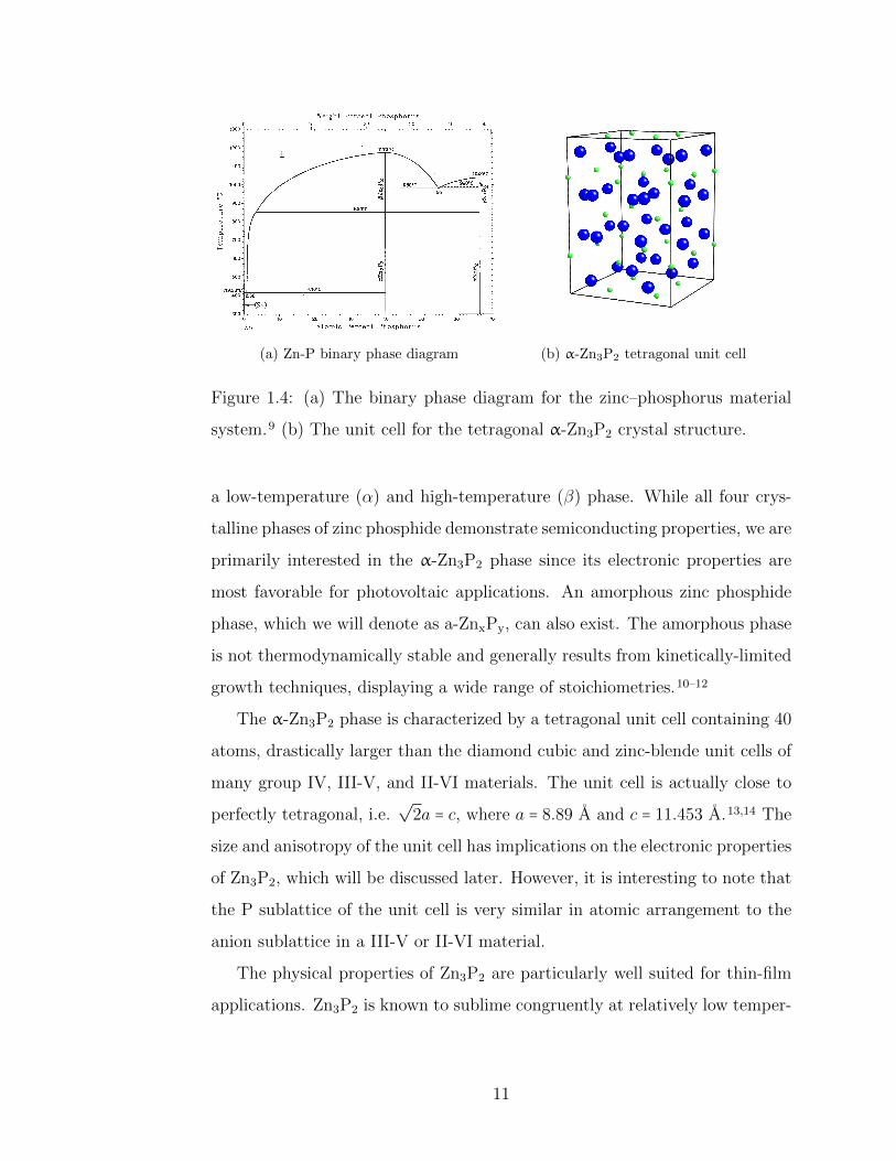
(a) Zn-P binary phase diagram (b) α-Zn3P2 tetragonal unit cell
Figure 1.4: (a) The binary phase diagram for the zinc–phosphorus material
system.9 (b) The unit cell for the tetragonal α-Zn3P2 crystal structure.
a low-temperature (α) and high-temperature (β) phase. While all four crys-
talline phases of zinc phosphide demonstrate semiconducting properties, we are
primarily interested in the α-Zn3P2 phase since its electronic properties are
most favorable for photovoltaic applications. An amorphous zinc phosphide
phase, which we will denote as a-ZnxPy, can also exist. The amorphous phase
is not thermodynamically stable and generally results from kinetically-limited
growth techniques, displaying a wide range of stoichiometries.10–12
The α-Zn3P2 phase is characterized by a tetragonal unit cell containing 40
atoms, drastically larger than the diamond cubic and zinc-blende unit cells of
many group IV, III-V, and II-VI materials. The unit cell is actually close to
perfectly tetragonal, i.e.√
2a = c, where a = 8.89 A and c = 11.453 A.13,14 The
size and anisotropy of the unit cell has implications on the electronic properties
of Zn3P2, which will be discussed later. However, it is interesting to note that
the P sublattice of the unit cell is very similar in atomic arrangement to the
anion sublattice in a III-V or II-VI material.
The physical properties of Zn3P2 are particularly well suited for thin-film
applications. Zn3P2 is known to sublime congruently at relatively low temper-
11

atures (< 800C) according to the following reaction:15
Zn3P2(c)→ 3 Zn(g) + 1
2P4(g), ∆H
700C = 144.4(4) kcal mol−1. (1.4)
Congruent sublimation and low-temperature processing greatly simplify large-
scale thin-film deposition and have been a key component to the success of
CdTe photovoltaics. Zinc phosphide compounds are also relatively benign
to the environment,* decomposing to zinc oxide, hydroxide, and phosphate
compounds:16
Zn3P2 + excess H2O,O2 Ð→ ZnO,Zn(OH)2 ,Znx(PO3)y,P4O10. (1.5)
Finally, elemental Zn and P are abundant and available at low costs compared
to other semiconductor precursors (see Figure 1.2).
1.2.2 Optical properties
The light absorption properties of Zn3P2 are the most relevant to its applica-
tion as a PV material. Zn3P2 has a high visible light absorption coefficient
(α > 1×104 cm−1) near its band edge, with 90% of light absorbed in the first 10
µm of the material.17 The absorption onset for Zn3P2 occurs around 1.4 ∼ 1.5
eV. This is near the optimal value of 1.35 eV for a single junction device under
terrestrial insolation.18
The absorption properties of any semiconductor are dominated by its elec-
tronic band structure. Figure 1.5 displays the band diagram for Zn3P2 as
calculated by hybrid density functional theory (DFT).19 The band properties
of the Zn3P2 are also complicated by the size of the unit cell. Interestingly,
*Interestingly, a large body of research (as in the vast majority of academic publications
on Zn3P2) has gone into investigating the effect of Zn3P2 on the environment due to its main
use as a common commercial rodenticide. A rodenticide is a material used to exterminate
rodents via ingestion. Zn3P2 does this by generating toxic PH3 gas upon interaction with
an aqueous acidic solution, e.g. stomach acid.
12
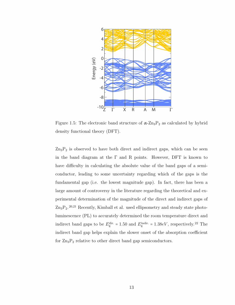
Figure 1.5: The electronic band structure of α-Zn3P2 as calculated by hybrid
density functional theory (DFT).
Zn3P2 is observed to have both direct and indirect gaps, which can be seen
in the band diagram at the Γ and R points. However, DFT is known to
have difficulty in calculating the absolute value of the band gaps of a semi-
conductor, leading to some uncertainty regarding which of the gaps is the
fundamental gap (i.e. the lowest magnitude gap). In fact, there has been a
large amount of controversy in the literature regarding the theoretical and ex-
perimental determination of the magnitude of the direct and indirect gaps of
Zn3P2.20,21 Recently, Kimball et al. used ellipsometry and steady state photo-
luminescence (PL) to accurately determined the room temperature direct and
indirect band gaps to be Edir.g = 1.50 and Eindir.
g = 1.38eV , respectively.22 The
indirect band gap helps explain the slower onset of the absorption coefficient
for Zn3P2 relative to other direct band gap semiconductors.
13

1.2.3 Electronic properties
In addition to strong light absorption, it is crucial that a PV material has the
necessary electronic properties to facilitate the collection of photo-generated
electron-hole pairs. This is typically determined by the minority-carrier diffu-
sion length, L. The diffusion length is a function of the carrier lifetime and
mobility according to the following expression:5
L =√Dτ =
õkBT
qτ . (1.6)
For thin-film applications, it is desirable for the absorber to have a diffusion
length that is on the order of the film thickness. In the case of a p-type semi-
conductor like Zn3P2, the electron diffusion length dominates the collection
efficiency of the PV device. Catalano et al. performed electron-beam induced
current (EBIC) and spectral response measurements on Mg-Zn3P2 Schottky
diodes (fabricated on both bulk and thin-film Zn3P2) and observed an Ln in
the range of 3 to 7 µm.23,24 More recently, Kimball et al. used time-resolved
photoluminescense (TRPL) to study the minority carrier lifetime (τn) in p-type
wafers.25 They found the value of τn to be approximately 20 ns, suggesting
diffusion lengths of > 7 µm, in excellent agreement with the Catalano work.
The large diffusion length makes Zn3P2 suitable for a PV device. It is also
interesting to note that the electron diffusion length observed in Zn3P2 is much
greater than that observed in other common polycrystalline thin-film absorber
materials. For instance, the Ln typically observed for CIGS and CdTe films
are limited to < 2 µm.26,27 It is believed that the thermalization of carriers
from the direct to the indirect gap in Zn3P2 is responsible for the larger Ln,
resulting in lower bulk recombination rates.
14

1.2.4 Materials challenges
Some challenges still remain for implementation of Zn3P2 as a solar material.
For example, Zn3P2 is an intrinsic p-type semiconductor. To date, there is only
one report of n-type conductivity in Zn3P2.28 Materials that are p-type have
the added benefit of electron minority carriers with longer diffusion lengths
than holes carriers due to the higher mobility of the electron. However, trou-
ble obtaining low-resistivity n-type material has eliminated the possibility of
fabricating homojunction solar cells. Hence, prior studies have focused on
devices implementing either a metal Schottky junction or a heterojunction.
In addition to n-type conductivity, the interface properties of Zn3P2 junc-
tions are not well understood. It is believed that P dangling bonds or Zn
precipitates result in interface states that act as carrier traps.25,29 A high
density of interface states may lead to Fermi-level pinning, resulting in de-
creased photovoltaic response. For example, the interface trap density and
cross section for a ZnO/Zn3P2 junction was determined by Nayar et al. to be
1012 cm−2 and 10−13 cm2, respectively.30 They found that the surface prepa-
ration of Zn3P2 had a drastic effect on their device performance, but offered
no solutions to avoid such issues like low Voc. Bube and coworkers tried us-
ing a metal-insulator-semiconductor (MIS) structure to decrease the number
of interface traps. However, their studies on Al/Al2O3/Zn3P2 diodes showed
surface density of states as high as 1013 eV−1 cm−2.29
Fortunately, Kimball et al. recently demonstrated that the surface recom-
bination velocity of a Mg/Al2O3/Zn3P2 MIS structure could be substantially
decreased by chemical preparation of the Zn3P2 surface.25 They found that
by exposing the Zn3P2 surface to a 2% Br:MeOH etch, followed by a dilute
aqueous HF/H2O2/H2O etch and air exposure reduced the SRV from > 104
cm s−1 (the untreated surface) down to ∼ 2×103 cm s−1. The present work
explores additional ways to prepare Zn3P2 surfaces and interfaces in order to
overcome these challenges.
15

1.3 Review of prior Zn3P2 photovoltaic device
studies
The literature on Zn3P2 photovoltaic devices is extremely sparse compared
to other more established PV materials. However, there have been a handful
of studies on the performance of Zn3P2 absorbers. The fabrication of Zn3P2
homojunctions has been complicated by difficulties in creating low-resistivity,
n-type material due to the formation of self-compensating, p-type intrinsic
defects in the Zn3P2 crystal lattice.31,32 Hence, the majority of PV device in-
vestigations with Zn3P2 have focused on Schottky barrier or heterojunction
solar cells, with Table 1.1 listing the champion cell properties for devices that
have incorporated Zn3P2 as a solar absorber. These studies provide an impor-
tant basis for further development of Zn3P2 photovoltaics. The sections below
review and compare the performance of Zn3P2 PV devices demonstrated to
date.
1.3.1 Mg/Zn3P2 Schottky diodes
A Schottky structure is different from a typical semiconductor p-n junction in
that the potential barrier across the device is produced between a metal and
a semiconductor, instead of two semiconductors. The built-in potential of the
device is nominally a function of the metal work function, φM . However, in
the case of Zn3P2 the barrier height appears to be more a function of the heat
of reaction between the metal and absorber than φM .38 Mg/Zn3P2 Schottky
structures have demonstrated the highest solar energy-conversion efficiencies,
with values of ∼6% for devices fabricated on bulk Zn3P2 wafers and values of
4.3% for Zn3P2 thin films.24,33 Mg metal was chose due to both its low φ and
high phosphide heat of formation. Unfortunately, these devices were reported
to have a high concentration of interface trap states, therefore limiting the Voc
to < 500 mV due to Fermi-level pinning.29 In many cases, the Mg metal was
16

Tab
le1.
1:D
evic
epro
per
ties
ofch
ampio
nSch
ottk
yan
dhet
eroju
nct
ion
sola
rce
lls
that
uti
lize
da
Zn
3P
2phot
ovol
taic
abso
rber
.
Junct
ion
par
tner
Ban
dga
pE
lect
ron
affinit
y
Abso
rber
fab.
Dev
ice
area
Dev
ice
ef-
fici
ency
Op
en-c
ir.
volt
age
Diff
usi
on
volt
age
Shor
t-ci
r.
curr
ent
den
sity
Fill
fact
or
Eg
χA
ηV
oc
VD
Jsc
FF
[eV
][e
V]
[cm
2]
[%]
[mV
][m
V]
[mA
cm−
2]
Mg
24
...
3.6
PV
T0.
75.
9649
280
014
.93
0.71
Mg
33
...
3.6
CSS
1.0
4.3
430
1320
16.8
0.53
ITO
34
3.80
...
PV
T0.
062.
128
0...
18.4
0.4
ZnO
30
3.40
4.57
PV
T0.
022
1.97
260
780
110.
59
CdS
35
2.42
4.79
PV
T0.
091.
230
064
011
.10.
35
ZnSe
36
2.70
4.09
CSS
0.1
0.81
810
1480
1.55
0.5
ZnS
37
3.68
3.9
MB
E0.
350.
0178
0...
0.05
0.35
17

found to react with the Zn3P2 surface resulting in a poorly defined interfacial
region.39,40
While metal–semiconductor Schottky devices are simple to fabricate, they
are intrinsically less efficient than semiconductor–semiconductor junctions due
to lower attainable barrier heights and increased surface recombination. In
fact, the barrier height of a Schottky structure is limited to roughly two-
thirds of the band gap of the semiconductor.5 This limit can be increased
with the use of a metal–insulator–semiconductor (MIS) device, but still falls
short of the ideal Voc attainable with a semiconductor–semiconductor junction.
Optical absorption and reflection losses at the metal front contact also place
an upper limit on the attainable Jsc in photovoltaics based on a Schottky
barrier structure. The combined current density and voltage restrictions of the
Mg/Zn3P2 device thus present challenges to obtaining further improvements
in the PV device efficiency of such systems.
1.3.2 Heterojunction Zn3P2 solar cells
A preferable solution to the lack of n-type Zn3P2 is to create a heterojunction
PV device. Zn3P2 heterojunction solar cells have been fabricated by use of
common n-type emitters such as ZnO, Sn-doped In2O3 (ITO), CdS, ZnSe, and
ZnS.30,34–37 The properties of champion heterojunction solar cells made with
these emitters can also be found in Table 1.1. The solar energy conversion
efficiencies of these devices to date are less than ∼ 2%. Nevertheless, in some
cases the Voc and Isc values for certain devices surpass those of Mg/Zn3P2
Schottky diodes, suggesting that efficiency enhancements are possible through
the use of a heterojunction solar cell design. In general, the heterojunction
architecture provides a more promising path toward the development of effi-
cient Zn3P2 solar cells due to fewer fundamental limitations as compared to a
Schottky architecture.
18

Absorber growth & characterization
(Zn3P2 molecular-beam epitaxy)
Emitter selection(ZnS, ZnSe, ZnO, CdS)
Device fab. & characterization(IV under AM1.5 solar
illumination)
Alternative device design
Evaluate & repeat(If initial emitter choice is
non-optimal)
Fundamentals(Band alignment from XPS & DFT)
(MIS, p-i-n, & superstrate
devices)
Optimal Heterojunction
Design
Figure 1.6: The design flow for fundamental characterization and device opti-
mization of Zn3P2 heterojunction solar cells.
1.4 Scope of this thesis
The goal of this thesis is to explore the upper limit of solar conversion efficiency
achievable with a Zn3P2 absorber. We pursue this goal primarily through the
design and fabrication of an optimal Zn3P2 heterojunction solar cell. In the
process, we explore three key aspects of material growth, interface energetics,
and device engineering:
(1) Absorber Growth: Compound-source molecular-beam epitaxy (MBE)
is employed to grow the highest quality Zn3P2 thin films possible. Em-
phasis is on achieving control of both growth orientation and optoelec-
tronic properties such that they are suitable for photovoltaic applica-
tions.
(2) Fundamental Characterization: The energy-band alignments of epi-
taxial Zn3P2 and II-VI and III-V semiconductor interfaces are measured
19

in order to determine the most appropriate heterojunction partner for
Zn3P2.
(3) Device Fabrication: Various heterojunction device designs are as-
sessed based on the material constraints associated with both Zn3P2
and the II-VI semiconductors of interest.
20

CHAPTER 2
Growth of Zn3P2 by molecular-beam epitaxy
2.1 Introduction
The fabrication of an efficient p-n junction photovoltaic device places rigorous
quality requirements on the active light absorber. This fact is observed by
the extremely high purity Si and GaAs semiconductors used in commerically
available solar cells. Typical elemental purities are on the order of 99.99999%
(7N). The most efficient devices incorporate monocrystalline materials which
are either produced from a monolithic boule (as in the case of Si) or deposited
as a single-crystal film using an epitaxial growth technique (as in the case of
GaAs). The goal of this work is to produce the highest optoelectronic quality
Zn3P2 thin films possible. Below is a brief review of the various deposition
techniques that were previously employed in growing thin films of Zn3P2 of
varying degrees of quality.
Thermal evaporation: The congruent sublimation of Zn3P2 allows
for films to be deposited by simply subliming the material in a vacuum
environment with a growth substrate within line-of-sight of the source
21

material. Under the right conditions, stoichiometric, crystalline films
will form on the growth substrate. This technique is limited by the
resublimation of the film, which is a function of the substrate tempera-
ture. Catalano and Hall produced Zn3P2 thin films of reasonable elec-
tronic quality on glass substrates using thermal evaporation of Zn3P2
compound source material.41
Close-space sublimation (CSS): Similar to thermal evaporation, CSS
takes advantage of the fact that Zn3P2 sublimes congruently. However,
CSS is distinctly different from the thermal evaporation method in that
the deposition occurs with the source and substrate placed in extremely
close proximity, typically no more than several mm, and with a temper-
ature gradient of roughly 100 ∼ 200 C. The close proximity solves the
problem of resublimation of the deposited film since it is recycled back to
the source material. This allows for much higher substrate temperatures
as well as faster growth rates. Catalano and coworkers first reported on
depositing specular, pinhole-free films of Zn3P2 with large grain sizes (>1
µm) using the CSS technique.33
Hot-wall deposition (HWD): Hot-wall deposition is similar to ther-
mal evaporation except that the source flux travels through an additional
heating tube that is held at a different temperature (typically higher)
than the source material. The additional heating can influence the stick-
ing coefficient of the flux without modifying the evaporation rate. In par-
ticular, this can cause cracking of the sublimated phosphorus tetramer
(P4) to the phosphorus dimer (P2) which drastically increases its stick-
ing probability. Both Fuke et al. and Babu et al. achieved well oriented
Zn3P2 films grown of good optoelectronic quality on glass slides using
hot-wall deposition.42–45
Sputter deposition: Plasma-deposition techniques have been used to
deposit zinc phosphide films on a number of different occasions.10–12,46
22

Magnetron sputtering can be performed either with a sintered Zn3P2
target and an inert Ar working gas or a Zn target with a working gas
containing a phosphine (PH3) partial pressure. However, sputter depo-
sition typically results in amorphous films with optical properties that
deviate from the crystalline material.
Liquid-phase epitaxy (LPE): Liquid-phase epitaxy of Zn3P2 on InP
(001) has also been reported.47 Elemental Zn and P were dissolved in
a molten In solvent. They achieved oriented growth along the (224)
or (004) zone axis through control of the cooling rate of the solvent.
The resulting films were polycrystalline and had very high hole-carrier
concentrations (>1018 cm−3), consistent with the unintentional incorpo-
ration of In as an extrinsic p-type dopant. It was also possible that
the observed doping was due to unintentional diffusion of Zn extrinsic
dopants into the InP substrate, which would explain the significantly
higher hole mobilities that were measured in the Zn3P2.
Chemical vapor deposition (CVD): Chemical vapor deposition is
characterized by the vapor-phase transport of the elemental constituents
via an inorganic chemical precursor into a growth zone where films are
deposited. Russell and coworkers demonstrated the controlled growth of
Zn3P2 thin films using CVD with Zn vapor and PH3 and characterized
the fundamental growth mechanism.48,49 However, their films were not
of high enough electronic quality for fabrication of rectifying Schottky
devices.
Metalorganic chemical vapor deposition (MOCVD): The first
true example of Zn3P2 epitaxy was reported by Suda et al.50,51 using
MOCVD. Similar to CVD, MOCVD transports film precursors in the
vapor phase, but uses organic precursors. Suda and coworkers used
dimethyzinc (DMZ) and phosphine (PH3) gases as precursors for Zn and
P, respectively. Growth was performed on GaAs(001) and ZnSe(001)
23

substrates because these materials have a relatively small lattice mis-
match with the P sub-lattice in the tetragonal α-Zn3P2 unit cell (1.3%
and 1.0%, respectively). The epitaxial layers grew along the Zn3P2(001)
crystallographic orientation, independently of the substrate material,
and were three-dimensional in nature. Difficulties with the MOCVD
technique for growing Zn3P2 included a small growth temperature win-
dow under which the DMZ and PH3 precursors would properly decom-
pose and the resulting Zn3P2 film would not quickly sublime away. An
additional problem observed was stress cracks in the epitaxial films that
occurred due to expansivity mismatch between the substrate and film.
Molecular-beam epitaxy (MBE): Suda and coworkers also demon-
strated growth of Zn3P2 epilayers on GaAs(001) using molecular-beam
epitaxy (MBE) with separate elemental Zn and P sources.28 Similar to
MOCVD growth, the films produced using MBE were observed to be
three-dimensional in nature using reflection high-energy electron diffrac-
tion. However, they were able to demonstrate the only instance of n-type
conductivity in Zn3P2, which they attributed to a large excess of Zn in
the crystalline lattice (>10%).
2.2 Fundamentals of molecular-beam epitaxy
In order to obtain the highest quality films possible, MBE was chosen for the
growth of Zn3P2 films. This technique is characterized by very low growth
rates (∼1 A s−1) which promote the epitaxy of highly crystalline materials. In
order to achieve these low rates while still maintaining low impurity incorpo-
ration, an ultra-high vacuum (UHV) environment is required (P ≤ 1 × 10⁻⁹
Torr). Growth rate and composition control are determined by the flux of
impinging atoms on the substrate surface. An atomic flux is created using a
Knudsen type effusion cell (see schematic provided in Fig. 2.1a). Elemental
or compound source materials are loaded into the effusion cell and evaporated
24

or sublimed using resistive heating. The atomic flux (n) is controlled by the
source temperature according the the Knudsen equation as follows:52
n = αP vap(T )√2πMWRT
NA [atom m−2 s−1], (2.1)
where α and P vap are the evaporation coefficient and vapor pressure for a given
substance. The atomic flux results in a beam equivalent pressure (BEP) which
the growth substrate is exposed to and can be measured and tuned to affect
the resulting film properties.
Crucible
Resistive heating element + heat
shield
Electrical leads + support
Thermocouple
UHV feedthroughs
(a) (b)
Figure 2.1: Schematics of (a) a standard Knudsen effusion cell and (b) a reflec-
tion high-energy electron diffraction (RHEED) set up where an electron beam
is reflected off of a surface and the resulting diffraction pattern is collected.
In situ analysis of the epilayer growth is possible using reflection high-
energy electron diffraction (RHEED). RHEED works by reflecting a high-
energy electron beam off of the growth surface at incidence angles of 1 ∼ 3.
The diffracted beam is directed at a phosphor screen and images are collected
using a CCD (see Fig. 2.1b). Electron beam energies typically range from 10
to 30 keV and spot sizes are on the order of 100 µm. For a smooth, crystalline
surface, diffraction occurs on the two-dimensional (2D) grating composed of
25

the crystalline films surface atomic lattice and “streaks” are observed on the
RHEED screen, indicative of the symmetry of the surface lattice or reconstruc-
tion. For a rough, or 3D surface, transmission diffraction takes place, resulting
in “spot” patterns similar to an electron diffraction pattern. RHEED is a pow-
erful tool to determine the morphology and epitaxial relation of the film during
growth and is used extensively in the present work.
One of our initial goals was to achieve heteroepitaxial growth of Zn3P2.
Heteroepitaxy refers to the growth of an ideally monocrystalline film of one
substance on top of a monocrystalline substrate of a different substance. Het-
eroepitaxy is necessary when a monocrystalline substrate of the film material
is not available and offers an opportunity to control the orientation and de-
crease the defect density in the resulting film. There are three primary modes
of heteroepitaxial growth which are all dependent on the lattice mismatch,
defined in terms of the film (f) and substrate (s) in-plane lattice parameters
as:
f = 2∣af − as∣/(af + as). (2.2)
The primary growth modes are:52 Frank-van der Merwe or “layer-by-layer”
growth which occurs when the deposited material wets the substrate surface
and the film grows one monolayer at a time. This regime is typical of very
small values of f . The second mode is Volmer-Weber or “island” growth. This
highly three-dimensional (3D) growth is caused by very large values of f or
when there is insufficient bonding between the substrate and film. Finally,
Stranski-Krastanov or “S-K” growth is described by the deposition changing
from layer-by-layer to island growth after the first few monolayers. S-K growth
indicates a change in surface free energies with increasing film thickness. This
is often caused by a slow build up in strain due to intermediate values of f .
To obtain smooth, specular films, operating in a layer-by-layer growth regime
is advantageous.
26

2.3 Zn3P2 compound source
The following sections describe the synthesis and characterization of the Zn3P2
source material and compound effusion source that were used in subsequent
MBE growth experiments.
2.3.1 Synthesis of Zn3P2 from the elements
Due to the extreme purity requirements for molecular-beam epitaxy (>99.999%
or 5N), it was necessary to synthesize our own high-purity Zn3P2 material.*
Zn3P2 can be synthesized from elemental Zn and P through a high temperature
physical vapor transport (PVT) process. The synthesis procedure has been
outlined previously by several authors.53–55 The details of our specific PVT
procedure are illustrated in Figure 2.2a. First, stoichiometric quantities of Zn
shot (6N) and red P chunk (6N) are loaded into separate ends of a cylindrical
quartz ampule (2” diameter × 12” length). The P end of the ampule is carbon
coated prior to loading the material via a methane decomposition process.
The ampule is then sealed under vacuum at a pressure of ∼ 1 × 10⁻⁵ Torr and
is ready to be baked.
The high-temperature reaction takes place in a two-zone furnace and hap-
pens in several steps. Initially the carbon-coated end of the ampule is heated
to 550 C in order to convert all of the red P to liquid white P and P4 vapor.
Next, the Zn metal end and carbon-coated ends are raised to 850 C and 650
C, respectively. The 200 C temperature gradient is held for roughly 18 to
24 h. During this time, the Zn metal begins to sublime and react with the
vapor-phase P4. Due to the temperature gradient, eventually all of the reacted
Zn and P accumulate at the carbon-coated end of the quartz ampule, resulting
in a polycrystalline boule that is composed of phase-pure α-Zn3P2. After the
reaction period, both ends of the quartz ampule are allowed to cool to room
temperature before removal from the synthesis furnace. The quartz ampule is
*Current commercial sources of Zn3P2 are not available at purities higher than 99.9%.
27

P4
Zn
Zn
Zn
ZnZn
ZnZn
Zn
Zn
Zn
ZnZn
Zn
Zn
Zn
ZnZn
ZnZn
ZnZn
Zn Zn
ZnZn
550oC
650oC 850oC
650oC 850oC
Zinc metal shot (6N)
Vacuum sealedQuartz tube
Red phosphorus chunk (6N)
Carbon coating
Zn3P2 Product
Cool down
Temperature gradient
Bake for 12 ~ 18 hrs
(a)
High-temp.Inconel Bomb
Two zone furnace
Tem
p. g
rad
ien
t
Ventedcaps
Top-view
Synthesis ampule
16
Seco
nd
ary
bla
st s
hie
ld, ¼
’’ St
ain
less
ste
el(b)
Figure 2.2: (a) The physical vapor transport (PVT) process for synthesizing
phase-pure Zn3P2 from the elements. (b) Furnace setup and shielding for
protection against accidental quartz ampule failure and P4 explosion.
then broken in half in order to remove the Zn3P2 boule. The boule is ground
into a fine powder using a mortar and pestle and then placed through an ad-
ditional PVT process for further purification. The resulting Zn3P2 material is
of roughly 5N purity according to ICP-MS analysis.56
The pyrophoric nature of elemental phosphorus necessitates that the PVT
process above be performed in a very controlled fashion. White phosphorus
vapor reacts with oxygen spontaneously to form phosphate according to the
following reaction:
P4(v) + 5 O2(v) Ð→ P4O10(s), (2.3)
where the heat and free energy of formation are ∆H
f = −2984 kJ/mol and
∆G
f = −2690 kJ/mol, respectively.57 If the quartz ampule fails at any point
during the high temperature procedure, any P4 in the vapor phase reacts
28

immediately resulting in an explosion. In fact, a number of ampule explosions
have occurred during the initial scale-up of the Zn3P2 synthesis procedure.
Most of these failures happened during the cool down process, in which the
Zn3P2 boule contracts in volume. If the ampule is not properly carbon coated,
the Zn3P2 adheres to the ampule and causes it to crack, exposing any remaining
P4 vapor to atmosphere.* Therefore, we have contained the synthesis ampule
within an Inconel pipe that sits directly inside of the two zone furnace. The
pipe has vented end caps in order to avoid pressurization. Finally, the entire
furnace is surrounded by a secondary blast shield made of stainless steel. An
illustration of the furnace setup and blast shield is displayed in Figure 2.2b.
2.3.2 Zn3P2 compound effusion source
The synthesized Zn3P2 material was loaded into a compound-source effusion
cell with an additional cracking zone. The cracking zone was intended to
convert phosphorus tetramer species (P4) into the dimer species (P2). The
dimer species was believed to be favorable for two main reasons. First, P4
condensation produces white phosphorus which, as mentioned earlier, is a
pyrophoric substance whose accumulation within the growth chamber could
be potentially dangerous. On the other hand, the P2 species condenses as solid
red phosphorus, a considerably more stable, and therefore safer compound.
Furthermore, since P2 has a larger sticking coefficient than P4, the use of a
cracker makes the source more efficient.
Prior to any growth studies, the Zn3P2 effusion cell performance was eval-
uated. First, the beam equivalent pressure (BEP) of the cell was measured
as a function of source temperature at the maximum cracker temperature of
*The most violent explosion took place during our first attempt to synthesize ZnP2,
which requires temperatures >950 C and nearly twice as much red P reactant. In this
case, the quartz ampule simply over-pressurized with P4 vapor causing it to pop and then
immediately combust. The remnants of the explosion was a large plume of thick white
smoke and a pile of pulverized quartz.
29

1.2 1.3 1.4 1.510
−10
10−9
10−8
10−7
10−6
10−5
1/T [×1000 K−1]
Ion
gaug
e pr
essu
re [T
orr]
T(cracker) = 1000 °C
Beam pressure (BEP)Background pressure
(a)
400 600 800 10000
0.2
0.4
0.6
0.8
1
Cracker Temperature [°C]
PP
4/(P
P2+
PP
4)
T(source) = 350 °C
ThermodynamicsExp. data
(b)
Figure 2.3: (a) Zn3P2 compound source effusion cell BEP as a function of the
inverse source temperature. (b) Partial pressure ratio of phosphorus tetramer
(PP4) to total phosphorus pressure (PP2 + PP4) exiting the compound-source
effusion cell versus cracker temperature.
1000 C. The BEP was determined using a standard nude ionization gauge
located within the Zn3P2 beam path and was uncorrected for differing ion-
ization gauge sensitivities of Zn and P2 vapor species. The measured BEP
is displayed in Figure 2.3a as a function of the inverse of the source tem-
perature. The experimental data are well fitted to the following equation:
log10(BEP) = 3.4148 − 5971.5 × T −1source. The open circles correspond to the
chamber background pressure during source operation. At typical growth
source temperatures (330 ∼ 380 C), the background pressure was approxi-
mately two orders of magnitude lower than the Zn3P2 BEP, which ensures a
relatively low rate of impurity incorporation.
Additionally, the ratio of the partial pressure of P4 to the total phosphorus
pressure (PT = P2 + P4) exiting the source is plotted in Figure 2.3b as a
function of the cracker temperature. For this experiment, the Zn3P2 source
temperature was held at 350 C. The partial pressures of the P, P2, P3, and P4
30

species were monitored in situ using a quadrupole mass-spectrometer located
within the beam path. It is clear that the thermal treatment converts P4 to
P2 species beginning at approximately 400 C, and complete conversion occurs
above 750 C. Given the equilibrium constant (KP ) for the reaction between
dimer and tetramer species as9
KP = exp(−∆G
RT) = exp(−229500 + 154.5 × T + 0.00313 × T 2 [J mol−1]
RT) ,
(2.4)
the ratio of PP4 /PT can be calculated from thermodynamics as follows:
PP4
PT= 1 + KP
2PT−
√K2P + 4KPPT
2PT. (2.5)
The above equation assumes that vapor phase Zn atoms do not interact with
P2 and P4 species, which is a good assumption since gaseous Zn3P2 molecules
have not been observed. The predicted ratio can also be found in Figure 2.3b.
One can see that good agreement was found between the observed partial
pressure ratio and the ratio estimated from thermodynamics. Some deviation
from theory occurs at lower cracker temperatures, due to P4 contributions in
the P2 mass spectrometer peak.*
2.4 Epilayer growth
The following sections describe the process by which Zn3P2 heteroepitaxy was
achieved. It was necessary to choose a suitable substrate for epitaxy as well
as a technique for preparing the substrate surface. Following which, RHEED
experiments were used extensively to evaluate our initial growth results. Based
on these findings the growth conditions were modified, resulting in high-fidelity
*The quadrupole mass spectrometer employs a thorium-iridium oxide filament that op-
erates at nearly ∼2000 C, which is more than hot enough to result in additional cracking
of the phosphorus tetramer to the dimer as well as monoatomic species.
31

growth.
2.4.1 Heteroepitaxial substrate
The two most important parameters for heteroepitaxy are the lattice mis-
match and thermal expansivity mismatch between the substrate and epilayer
materials. As mentioned earlier, the lattice mismatch dominates the growth
mechanism and a small lattice mismatch provides an opportunity to decrease
interfacial and bulk defects in the epilayer. The thermal expansivity mismatch
between the substrate and epilayer becomes important when the growth tem-
perature is far from room temperature (> 300 C). Contraction in either the
substrate or epilayer during cooling can result in microcracks in the epilayer.
Microcracks were seen previously for MOCVD growth of Zn3P2.50 Ideally, the
substrate material should be both well lattice matched and thermal expansiv-
ity matched to the epilayer material. We reviewed a large number of materials
and compared their lattice parameters and expansivity coefficients with those
of Zn3P2 (See Figure A.1 in section A.1). Of those materials, the GaAs(001)
surface was chosen as the substrate for epitaxial growth since the phosphorus
sub-lattice of Zn3P2 is similar to that of arsenic with a room-temperature lat-
tice mismatch lower than 1.3%. Other possible substrate candidates included
ZnSe and Ge, with 1.0% and 1.2% lattice mismatches, respectively. Despite
having better lattice match, both materials were ruled out due to other issues;
conductive ZnSe substrates are not widely available and the non-polar surface
of Ge complicates the heteroepitaxy of polar compounds such as Zn3P2.
Several different methods were attempted to prepare the GaAs(001) surface
prior to Zn3P2 growth. The goal of the surface preparation was to remove the
GaAs native oxide, leaving a clean, atomically smooth surface for subsequent
growth. Initially, a chemical etching procedure was adopted based on literature
reports.58 The etching procedure involved three steps:
(1) H2SO4:H2O2:H2O (4:1:100) for 2 min in order to remove any adventitious
32

carbon contamination from the surface.
(2) HCl:H2O (3:1) for 2 min to remove Ga2O3 and Ga2O surface species,
leaving behind an As-terminated surface.
(3) DI-H2O rinse and nitrogen blow dry.
However, the wet etch process failed to completely remove the GaAs native
oxide and also resulted in increased surface roughness based on RHEED im-
ages.
The second technique adopted was to simply anneal the GaAs substrate
at a temperature slightly above its congruent sublimation temperature (∼580
C), which results in decomposition of the native oxide. The anneal takes
advantage of the fact that Ga2O3 will react with subsurface GaAs to form
Ga2O according to:59,60
Ga2O3(s) + 4 GaAs(s) Ð→ 3 Ga2O(v) + 2 As2(v)/As4(v). (2.6)
Both the Ga2O and As4 product species sublime readily at temperatures >400 C, leaving behind an oxide-free GaAs surface. This procedure worked
considerably better than the wet chemical etch. However, the anneal resulted
in large etch pits in the GaAs surface due to Ga2O3 consuming the subsurface
GaAs. The anneal procedure also leaves a largely Ga-terminated surface, with
some formation of liquid Ga droplets.
The final, and most successful method for removing the GaAs native oxide
was via exposure of the surface to an atomic hydrogen plasma.61 Atomic H is
capable of reducing the Ga2O3 to Ga2O and As2Ox to elemental As at temper-
atures of 400 C < Tsub < 500 C, according to the following reactions:60,62,63
Ga2O3(s) + 4 H (v) Ð→ Ga2O(v) + 2 H2O(v), (2.7)
As2Ox(s) + 2x H (v) Ð→ x H2O(v) +As2/1
2As4. (2.8)
33

Surface Preparation Comparison
(a) Wet chemical etch
(b) 620 oC thermal anneal
(c) Atomic hydrogen treatment
Figure 2.4: In situ RHEED images of the GaAs(001) after (a) wet chemical
etching, (b) a 620 C thermal anneal, and (c) a 20 min exposure to an atomic
hydrogen flux at 450 C.
The low temperature reduction drastically limits the reaction of the oxide
with subsurface GaAs therefore limiting the formation of both pits and liquid
Ga droplets. A comparison of RHEED images for the three different substrate
preparation methods is displayed in Figure 2.4. Clearly, the streakiest RHEED
pattern was obtained for the atomic H treatment, indicating a smoother GaAs
surface. Atomic H preparation of the GaAs(001) surface was used for all
subsequent experiments reported in this work.
2.4.2 Initial growth results
Preliminary growth studies were performed using the Zn3P2 compound source
with high cracker temperatures (>800 C) in order to guarantee efficient phos-
phorus incorporation in the deposited films. However, this strategy alone
resulted in amorphous films with P-rich stoichiometry. Varying the substrate
temperature did not produce crystalline films but strongly affected the growth
rate. Crystalline films were obtained when an additional Zn flux was added
to the growth recipe. Figure 2.5 shows RHEED patterns recorded at different
time intervals during the growth under three Zn fluxes. For all three growths
the Zn3P2 BEP and substrate temperature were held constant at 1×10⁻⁶ Torr
and 350 C, respectively. At low Zn BEP (left column), the RHEED patterns
were hazy with diffuse spots, indicative of a primarily amorphous film growth.
34

60 min
3 min
0 min
Zinc atomic flux
Gro
wth
tim
e
4.5×10⁻⁷Torr 6.2×10⁻⁷Torr 8.5×10⁻⁷Torr
Zn3P2 BEP = 1.0×10⁻⁶ Torr, Tsub. = 300oCFigure 2.5: In situ RHEED images of Zn3P2 epitaxial growth on GaAs(001) at
different additional Zn BEP. All of the growths were performed at a substrate
temperature of Tsub. = 350 C and Zn3P2 BEP of 1 × 10⁻⁶ Torr. Images were
recorded along the GaAs [011] zone axis.
At higher Zn BEP (middle column), the background remained hazy while a
more complex spot pattern was observed. The complex pattern is likely due to
uncontrolled crystal twining resulting in multiple grain orientations. Finally,
for the highest Zn BEP (right column) a sharp spot pattern was observed,
indicative of a highly crystalline and oriented film with a rough surface.
The higher overpressure of Zn metal required to obtain crystalline Zn3P2
films is rather counter intuitive. Growth of group III-V phosphide materials
like GaP and InP normally require extremely high overpressures of phosphorus
(PV:PIII ∼ 30:1) in order to obtain stoichiometric material. The difference be-
tween typical III-V growth and Zn3P2 growth is that the Zn vapor pressure is
much higher than that of a group III element, resulting in a much lower com-
parative sticking coefficient and thus a more stoichiometric beam composition
is required.
The spot pattern obtained from higher Zn fluxes resembles that of a trans-
35

(i) [1-10]
(ii)
(iii)
[100]
[110]
α-Zn3P2(001)
surfaceRHEED
incidence
α-Zn3P2
unit cell
[100][010]
[001]
Zn
P
(1)
(2)
(ii)
(iii)
(i)(3)
Figure 2.6: (a) α-Zn3P2 unit cell, (b) in-plane atomic arrangement of the α-
Zn3P2(001) surface. (c) Comparison of RHEED patterns of the (001) surface
with along different zone axes with electron diffraction simulations for the
α-Zn3P2 tetragonal crystal structure.
mission electron diffraction pattern, indicating that the growth was three-
dimensional. While 3D growth is not necessarily desirable for obtaining high
quality films, it does allow the use of the RHEED patterns to determine the
in-plane epitaxial relationship between Zn3P2 and GaAs. RHEED patterns
taken for three different zone axes of the Zn3P2 film are displayed in the left
column Figure 2.6. The right column shows simulated electron diffraction pat-
terns for the same zone axes assuming a tetragonal crystal structure.64 From
the RHEED patterns, a 45 in-plane rotation about the Zn3P2(001) direction
is observed with respect to GaAs. Hence, the epitaxial relationship between
the epilayer and the substrate was Zn3P2(004) ∣∣ GaAs(002) and Zn3P2(202)
∣∣ GaAs(111). This rotation occurs because it results in a slight decrease in
lattice mismatch between the Zn3P2 and GaAs.
36

2.4.3 Two-dimensional growth
An additional way to obtain crystalline films of Zn3P2 was to decrease the
effusion source cracker temperature. At cracker temperatures < 500 C, the
vapor-phase phosphorus is composed predominately of the P4 species, which
has a much lower sticking coefficient than the P2 species. Figure 2.7 displays
RHEED images collected along the [100] zone axis of Zn3P2 films that were
grown with a cracker temperature of 450 C and at substrate temperatures of
150 C, 200 C, and 250 C, respectively. The RHEED images of Zn3P2 films
that were grown at 200 ∼ 235 C exhibited streaky (1×1) patterns, indicating
highly crystalline, oriented film growth that occurred two-dimensionally. The
faint appearance of half-order streaks in the RHEED patterns suggested that
a partial surface reconstruction occurred for thicker films. The reconstruction
is consistent with Zn-termination of the Zn3P2(001) surface. All RHEED
images observed for films that were grown at substrate temperatures < 175
C revealed cloudy, specular beam reflection with only a faint appearance of
crystalline peaks, indicating that the films were primarily amorphous. The
deposition of amorphous material established a practical lower bound of ∼ 200
C on the substrate temperature for Zn3P2 epitaxy. Spotty RHEED patterns
were observed for films that were grown at substrate temperatures of > 250
C, indicating that these films were crystalline and oriented, but that their
surfaces were significantly rougher than the surfaces of films that were grown
at lower temperatures. The observed increase in roughness is consistent with
the partial re-sublimation of the deposited Zn3P2 film along some preferred
orientation.
2.5 Conclusions
The growth of epitaxial Zn3P2 films was successfully demonstrated using com-
pound-source MBE. It was found that the cracking of P4 vapor species to
P2 was not favorable for the growth of films with smooth surfaces, which is
37

(a) Tsub. = 150 °C (b) Tsub. = 200 °C (c) Tsub. = 250 °C
[100] 1×10⁻⁶ Torr
Figure 2.7: RHEED images of Zn3P2 films grown at a substrate temperature
of (a) 150 C, (b) 200 C, and (c) 250 C.
in direct conflict with the conventional growth conditions used for epitaxy
of III-V phosphide materials. This discrepancy results from the difference in
sticking coefficients between a group III element and Zn metal. By employing
a stoichiometric flux, we were able to achieve a 2D growth regime which was
not observed in previous epitaxial growth studies of Zn3P2. Finally, RHEED
patterns were used to determine the epitaxial orientation between the Zn3P2
epilayer and the GaAs substrate. The subsequent chapters will examine the
properties of MBE grown Zn3P2 films in greater detail.
38

CHAPTER 3
Ex situ characterization of Zn3P2 epilayers
In addition to in situ RHEED measurements, the Zn3P2 epilayers were evalu-
ated using a number of ex situ characterization techniques in order to verify
the thin-film properties. The following sections describe our investigation of
the bulk, surface, and growth interface morphology as well as the optical and
electronic properties of pseudomorphic Zn3P2 films.
3.1 Growth rate and film morphology
Figure 3.1 displays the growth rate of Zn3P2 as a function of the substrate
temperature for a BEP of ∼ 1×10⁻⁶ Torr. The growth rate was calculated from
the film thickness and the growth length. The film thickness was determined
by profilometry. For substrate temperatures < 250 C, the growth rate was
typically 3 ∼ 4 nm min−1. For temperatures > 250 C, a rapid decline in
the growth rate was observed, consistent with a decrease in the Zn sticking
coefficient with increasing temperature. Analogous trends in growth rate have
been reported for Zn-containing II-VI compounds, such as ZnSe and ZnS.65,66
39

100 150 200 250 300 35010
−2
10−1
100
101
Growth Temperature [ °C ]
Gro
wth
rat
e [n
m m
in−
1 ]
Zn3P2, BEP=1.0×10⁻⁶ Torr
ZnS, BEP=1.5×10⁻⁶ Torr
Figure 3.1: The growth rate of Zn3P2 as a function of substrate temperature
for a given BEP of ∼1 × 10⁻⁶ Torr. The growth rate data for ZnS is displayed
for comparison.66 The optimal growth window for Zn3P2 epitaxy was between
200 C and 250 C, indicated by the vertical dotted lines.
For comparison, the growth rate of ZnS produced by compound-source MBE
under similar conditions is plotted along with the Zn3P2 data. The Zn3P2
growth rate decreased over a much narrower temperature range than has been
reported for growth of ZnS, with the Zn3P2 growth completely terminated
by 300 C. This behavior is expected, since within the temperature range of
interest Zn3P2 exhibits a much higher sublimation pressure than ZnS.15,67 To
allow for Zn3P2 epitaxy, the observed rapid reduction in growth rate establishes
a practical upper bound of ∼250 C on the substrate temperature.
The surface roughness of the as-grown films was verified by atomic force
microscopy (AFM) topography imaging (Figure 3.2). Films that were grown
between 200 ∼ 235 C had a typical RMS surface roughness of 0.6 nm, whereas
films that were grown at < 175 C or at > 250 C were significantly rougher,
having typical RMS roughness values of 2 nm and 10 nm, respectively. The
AFM topography results, in addition to the growth rate and RHEED images,
indicated that the growth of smooth, epitaxial Zn3P2 films was constrained
40

1 μm
5 μm
60 nm
0 nmZn3P2[010]
[110]
[100]
(a) Tsub. = 150 °C (a) Tsub. = 200 °C (a) Tsub. = 250 °C
Figure 3.2: AFM topography images of the Zn3P2 surface for films grown at
substrate temperatures of 150 C, 200 C, and 250 C, respectively. The height
scale bar applies to all of the AFM images.
to a narrow temperature window, specifically between 200 C and 235 C.
To maximize the growth rate and to minimize the surface roughness, all sub-
sequent growths were therefore performed at a substrate temperature of 200
C.
The crystallinity and orientation of the Zn3P2 epilayers were further verified
by high-resolution x-ray diffraction (HRXRD). Figure 3.3a displays symmetric
HRXRD spectra of the GaAs(004) and Zn3P2(008) reflections collected on
increasing epilayer thicknesses. Clear Pendellosung oscillations were observed
for film thicknesses of < 150 nm, indicating highly crystalline thin films. The
Pendellosung oscillations arise from optical interference of the x-rays due to
thin-film diffraction between the Zn3P2 epilayer surface and the Zn3P2/GaAs
interface. Table 3.1 reports the 2θ values of the Zn3P2(008) peak maximum
for all films. A shift in the Zn3P2(008) peak position with respect to the bulk
2θ position was observed for film thicknesses up to ∼ 150 nm.13 This shift
represents an out-of-plane strain (ε⊥) value of approximately 0.91%. For films
> 150 nm in thickness, the XRD indicated a partial relaxation of ε. However
for thicknesses up to 400 nm, 100% relaxation was not yet observed.
Figure 3.3b displays HRXRD double-axis rocking curves of the Zn3P2(008)
reflection for 70, 150 and 400 nm thick epilayers. The peak width of the rocking
41

63.5 64 64.5 65 65.5 66 66.5
102
104
106
108
1010
1012
GaAs(004)
Zn3P2(008) ε⊥ = 0.91%
Zn3P2(008) ε⊥ = 0%
20 nm
50 nm
100 nm
150 nm
400 nm
Inte
nsity
[a.u
.]
2θ [degrees]
(a)
−1000 0 100010
0
102
104
106
70 nm
150 nm
400 nm
16 arcsec
52 arcsec
966 arcsec
Inte
nsity
[a.u
.]
ω [arcsec]
(b)
Figure 3.3: (a) Symmetric HRXRD scans of the Zn3P2(008) and GaAs(004)
reflections for increasing Zn3P2 layer thickness. Vertical dashed lines represent
the Zn3P2 peak positions for a fully strained and relaxed unit cell. (b) Rocking
curves of the Zn3P2(008) reflection for film thicknesses of 70, 150, and 400 nm.
curve is considered a good indication of the crystallinity of the epilayer, with
narrower widths equivalent to higher crystallinity. The rocking curve of the 70
nm film was composed of a narrow, coherent scattering peak with a FWHM
of 16 arcsec, as well as a low-intensity diffuse scattering feature. A diffuse
scattering peak is often observed in epitaxial layers and is associated with the
presence of point defects.68 A broadening in the rocking curve was observed
for the 150 nm and 400 nm films, with the peak FWHM values increasing
to 52 arcsec and 966 arcsec, respectively. This broadening is expected as the
in-plane lattice parameter of the epilayer relaxes towards its native value. The
relaxation process is normally accompanied by the creation of defects within
the film.
Further evidence of pseudomorphic epilayer growth and strain relaxation
was obtained from reciprocal space maps of the GaAs(113) and Zn3P2(206)
asymmetric reflections that were collected for the 70 nm, 150 nm, and 400
42

Qz
(a)70 nm70 nm
GaAs(113)GaAs(113)
Zn3P2(206)Zn3P2(206)
−1.6 −1.55
3.25
3.3
3.35
3.4
Qx
(b)150 nm150 nm
−1.6 −1.55
(c)400 nm400 nm
−1.6 −1.55
Figure 3.4: Reciprocal space maps of the Zn3P2(206) and GaAs(113) asym-
metric reflections for Zn3P2 film thicknesses of (a) 70, (b) 150, and (c) 400
nm. The red dot in (c) represents the position of the fully relaxed Zn3P2(206)
reflection in reciprocal space.
nm thick films (Figure 3.4). A relaxation of the in-plane lattice parameter of
the Zn3P2 epilayer was clearly evident by the comparison of the three mea-
surements. The reciprocal space map of the 70 nm film showed a coherently
strained Zn3P2 peak with respect to the GaAs substrate. The onset of relax-
ation was also observed for the 150 nm film, with a noticeable broadening of
the film peak. Finally, the 400 nm film peak was further broadened in the
direction of the calculated position for a fully relaxed film (red dot).
The microstructural changes incurred in the Zn3P2 epilayers upon relax-
ation were investigated using transmission electron microscopy (TEM). Fig-
ure 3.5 (a) and (b) display bright-field TEM images of the 50 and the 150 nm
thick Zn3P2 epilayers, respectively. The 50 nm epilayer was effectively dislo-
cation free, in agreement with both the coherent strain and extremely sharp
rocking curves observed with HRXRD. On the other hand, a low concentration
of crystalline defects was observed for the 150 nm thick film, further indicating
the onset of strain relaxation. The red arrow in Figure 3.5 (b) points to the
initiation of a threading dislocation in the epilayer. For a lattice mismatch
of 1.3%, such dislocations are unavoidable for growth of thick films and will
43

Zn3P2
GaAs
(a)
Zn3P2
GaAs
(b)
Figure 3.5: Bright field transmission electron micrographs of pseudomorphic
Zn3P2 layers with thicknesses of (a) 50 nm and (b) 150 nm. The red arrow in
(b) indicates the initiation of a threading dislocation due to the onset of strain
relaxation.
likely degrade the electronic properties of the Zn3P2 to some extent.
3.2 Surface and interface characterization
In order to explore the properties of Zn3P2 epitaxy, high-resolution TEM im-
ages of the Zn3P2/GaAs interface as well as scanning tunneling microscopy
(STM) images and x-ray photoelectron spectra of the initial stages of Zn3P2
growth were collected. The TEM images were collected by Dr. Steve Rozeveld
of the DOW Chemical Company and the STM images were collected on fresh
Zn3P2 surfaces grown on GaAs by Dr. Seokmin Jeon.69 More details of the
STM characterization of Zn3P2 surfaces can be found in Dr. Jeon’s Ph.D.
thesis.70
Figure 3.6 (a) shows a high-resolution TEM image of the Zn3P2/GaAs(001)
interface revealing crystalline, atomic order with (001) out-of-plane orientation
for both the substrate and the epilayer. The out-of-plane bilayer spacing across
the interface (Figure 3.6 (b)) was calculated by averaging the image contrast
across the atomic layers and determining the distance.* Both the GaAs and
*The bilayer spacing was actually calibrate to the known lattice parameter of the GaAs
44

Zn3P2 bilayer spacings were in excellent agreement with the values calculated
from the known lattice constants of each crystal structure (black lines). How-
ever, near the interface the bilayer spacing dramatically decreased. The small-
est bilayer spacing observed matched the expected spacing of a GaP lattice
which was under tensile strain due to the larger GaAs in-plain lattice constant
(red dotted line). We believe this was evidence of a tetragonally-strained GaP
interfacial layer between the GaAs substrate and the Zn3P2 epilayer. The
thickness of the interfacial layer was difficult to accurately determine since
changes in the bilayer spacing did not occur in discreet steps. However, the
thickness appears to be on the order of 1 ∼ 2 nm. Finally, slight increases in the
Zn3P2 and GaAs bilayer spacings directly adjacent to the interface were also
observed (black arrows), indicating that the strained GaP layer caused some
tetragonal compressive strain to occur in the adjacent epilayer and substrate.
The schematic diagram in Figure 3.7 displays STM images and our pro-
posed film growth mechanism of Zn3P2 on the Ga-rich GaAs(001) using com-
pound-source MBE. Initiation and growth occurs in several steps:
(i) The GaAs(001) surface prepared by either atomic hydrogen cleaning or
inert ion sputtering displays the Ga-rich GaAs(6×6) reconstruction.
(ii) P4 vapor decomposes and bonds to the surface Ga atoms changing the
surface to a P-dimer terminated surface with either the β2(2×4) or
δ(2×4) reconstructions. XPS indicates that these surface reconstructions
are those of the GaP(001) surface based on the P 2p core-level shift.*
(iii) The formation of a GaP surface layer was followed by the formation of
featureless islands with random locations on the surface, indicating the
growth of a P-rich ZnPx (x > 1) amorphous overlayer.
bulk, far away from the Zn3P2/GaAs interface*DFT simulations performed by Dr. Jeon predicted that the replacement of subsurface
As atoms by P atoms is an exothermic process, causing the formation of a GaP interfacial
layer up to several monolayers thick.
45

Zn3P2c = 1.145 nm
GaPa = 0.545 nm
GaAsa = 0.563 nm
Figure 3.6: (a) High-resolution TEM image of the Zn3P2(001)/GaAs interface
showing the presence of a GaP interfacial layer. (b) The calculated bilayer
spacing across the interface. The black lines represent the bilayer spacing for
the Zn3P2 and GaAs lattices. The black and red dotted lines represent the
bilayer spacing for unstrained and strained GaP, respectively. The blue, gray,
green, and violet spheres in the structure model represent Zn, Ga, P, and As
atoms, respectively.
(iv) Under further Zn and P flux, an epitaxial Zn3P2 film grows below the
amorphous overlayer. However, the surface of the Zn3P2 epilayer remains
covered by the amorphous overlayer with a total thickness of ∼ 1 nm.
Formation of the P-rich overlayer is likely due to the low sticking coefficient
of Zn as compared to P on the Ga-rich GaAs(001)-(6×6) surface, especially at
low Zn3P2 coverage. Thus, the film growth is expected to be limited by Zn
adsorption.
3.3 Optical properties
The optical properties of the epitaxial Zn3P2 films were determined using spec-
troscopic ellipsometry. Figure 3.8 displays the wavelength dependence of the
46

Ga-rich GaAs(001)
Ga Ga Ga
Ga Ga Ga
P P P
Zn PP
GaAs(001)
Amorphous ZnPx
GaP
Ga Ga Ga
P P PP P
GaP(001)-B2(2x4)
Zn3P2/GaAs Growth Mechanism
Pseudomorphic
α-Zn3P2
GaAs(001)(6x6)
( i ) ( ii ) ( iii ) ( iv )
ZnPx Overlayer
TEM
Figure 3.7: STM images of the initial stages of Zn3P2 growth on the Ga-
rich GaAs(001) surface. A proposed model for the growth mechanism is also
displayed.
index of refraction (n) and the extinction coefficient (k), as determined on a
7 µm thick Zn3P2 film. The measured values of k also allow determination
of the energy dependence of the absorption coefficient (α = 4πλ/k) of Zn3P2.
Figure 3.8 (b) and (c) display α2 and α1/2 plotted versus photon energy, near
the band edge of Zn3P2. Extrapolation of the linear regions of the data yielded
values for the direct and indirect band gaps of Zn3P2 of 1.52 eV and 1.39 eV,
respectively. These values are in excellent agreement with those previously
obtained on bulk Zn3P2 wafers.22 The effect of crystalline relaxation on the
optical properties could not be directly observed since thin films (< 3 µm) of
Zn3P2 were not fully absorbing near the band edge, which led to interference
with the GaAs substrate. Our attempts to study the photoluminescence prop-
erties of Zn3P2 epilayers were also hindered by the luminescence of the GaAs
substrate.
3.4 Electrical properties
The electrical properties of the Zn3P2 epilayers were determined using a com-
bination of van der Pauw and Hall effect measurements. First, the intrinsic
47

(a) (b)
(c)
1.52 eV
1.39 eV
Figure 3.8: (a) The index of refraction (n) and extinction coefficient (k) values
obtained by spectroscopic ellipsometry on a 7 µm thick Zn3P2 film. The linear
extrapolation of (b) α2 and (c) α1/2 as a function of energy resulted in direct
and indirect transition values of 1.52 eV and 1.39 eV, respectively.
conductivity of as-grown Zn3P2 samples was studied, followed by attempts to
incorporate extrinsic dopants with the goal of obtaining controllable p-type
and n-type doping. All measurements were performed on 6 mm × 6 mm sam-
ples with soldered In contacts.
3.4.1 Intrinsic doping
All of the as-grown Zn3P2 epilayers exhibited p-type conductivity. Figure 3.9
displays the resistivity, carrier concentration, and Hall mobility of Zn3P2 films
as a function of epilayer thickness. The electrical measurement results are also
tabulated in Table 3.1. The resistivity of the strained films was consistently
on the order of 1 Ω-cm, with corresponding hole concentrations of > 1 × 10¹⁷
cm−3. A large increase in resistivity, and consequent decrease in the hole carrier
concentration, was observed as the film thickness was increased above 150 nm.
The Zn3P2 hole mobility also varied as a function of the epilayer thickness.
For strained films, an increase in mobility was observed for increasing epilayer
thicknesses between 20 and 150 nm. This increase is consistent with a decrease
48

100
102
104
Res
istiv
ity[Ω
−cm
]
StrainedPartially relaxed
1014
1016
1018
Hol
e de
nsity
[cm
−3 ]
0 100 200 300 400 5000
20
40
60
Hol
e m
obili
ty[c
m2 V
−1 s−
1 ]
Film thickness [nm]
Figure 3.9: (a) Van der Pauw resistivity, (b) hole carrier concentration, and (c)
hole mobility as a function of Zn3P2 epilayer thickness. The filled and open
circles represent the data collected on strained and partially relaxed films,
respectively.
in sensitivity to the interfacial defects between the Zn3P2 epilayer and the
GaAs substrate. Similar trends have been observed for heteroepitaxial films of
InAs on GaAs,71,72 InSb on GaAs,73 and GaN on Al2O3.74 A maximum hole
mobility of ∼ 45 cm2 V−1 s−1 was observed for a strained 150 nm thick film.
This value is comparable to the maximum hole mobility reported for Zn3P2
single crystals that were grown by PVT.41,55 Upon partial relaxation of the
films, the hole mobility decreased to < 20 cm2 V−1 s−1, which is similar to
values previously reported for polycrystalline Zn3P2.22
49

Theoretical31 and experimental41 studies have indicated that the dominant
mechanism for intrinsic p-type conductivity in Zn3P2 is the presence of inter-
stitial phosphorus atoms. This hypothesis agrees well with the observation of
diffuse scattering peaks in the HRXRD rocking-curves of the pseudomorphic
Zn3P2 films. The diffuse scattering is indicative of point defects within the
epilayer, and in the case of Zn3P2 is consistent with the presence of intersti-
tial P atoms. A high level of interstitial P is also consistent with the high
concentration of hole carriers observed in strained films by the Hall effect. A
subsequent decrease in the hole carrier concentration and the hole mobility
upon film relaxation is consistent with the occurrence of misfit dislocations
and threading dislocations within the epilayers, as observed by TEM. Dis-
locations have been suggested to act both as charged-carrier scattering and
acceptor-compensating regions within a semiconductor material.75 Therefore,
a high density of threading dislocations within a partially relaxed Zn3P2 film
would be expected to compensate the P interstitials that are responsible for the
intrinsic p-type conductivity, and to thus decrease the effective hole mobility
by 50% or more.
3.4.2 Extrinsic p-type doping
Controlled p-type doping is valuable for PV fabrication since it allows for
improved device performance through both tuning of the built-in potential
and incorporation of a back-surface field for passivation. Extrinsic p-type
doping in Zn3P2 bulk crystals was previously reported using Ag impurities. In
these studies, Ag films were deposited and then annealed into the bulk of the
wafer at high temperatures (> 400 C), resulting in an increase in the acceptor
density. Hole concentrations on the order of ∼1×1017 cm−3 were achieved using
this method without a significant decrease in the hole mobility.
While diffusion doping has the merit of being simple and functional, it
results in a doping profile that is difficult to control. Our goal was to in-
corporate extrinsic Ag atoms into the Zn3P2 lattice during normal epilayer
50

Ag:ZnP BEP = 0.0
= 1.3×10-3
= 7.1×10⁻³
ZnS:ZnP = 1×10-2
= 2×10-2
= 5×10⁻²
I(Al) = 0.110 A
= 0.120 A
= 0.130 A
(a) Ag-doping
Ag:ZnP BEP = 0.0
= 1.3×10-3
= 7.1×10⁻³
ZnS:ZnP = 1×10-2
= 2×10-2
= 5×10⁻²
I(Al) = 0.110 A
= 0.120 A
= 0.130 A
(b) Al-doping
Ag:ZnP BEP = 0.0
= 1.3×10-3
= 7.1×10⁻³
ZnS:ZnP = 1×10-2
= 2×10-2
= 5×10⁻²
I(Al) = 0.110 A
= 0.120 A
= 0.130 A
(c) S-doping
Figure 3.10: RHEED images of Zn3P2 epilayers for increasing impurity in-
corporation of (a) Ag, (b) Al, and (c) S. For all growth the Zn3P2 BEP and
substrate temperatures were maintained at ∼1× 10⁻⁶ Torr and 200 C, respec-
tively.
growth, resulting in controllable p-type doping levels throughout the film.
Zn3P2 epilayers were grown with an increasing beam flux of Ag atoms. The
flux was supplied using an additional Knudsen effusion source loaded with 6N
Ag metal. Throughout all of the growths, the Zn3P2 beam flux was maintained
at ∼ 1 × 10⁻⁶ Torr and the ratio of the Ag to Zn3P2 flux is reported. RHEED
images collected during the growth demonstrated that the incorporation of
additional Ag at low ratios (Ag:Zn3P2 < 5×10⁻³) did not effect the orientation
of the Zn3P2 growth (Figure 3.10a). However, at higher Ag fluxes, the surface
of the film was roughened and a small amount of crystalline twinning was
observed, indicating the onset of Ag-alloying or possibly phase separation.
The electronic properties of Ag-doped films as grown, and after a series of
low-temperature vacuum anneals, were investigated using van der Pauw and
51

Hall effect measurements. Figure 3.11 displays (a) the thin-film resistivity as
well as (b) the hole mobility of undoped, lightly Ag-doped, and heavily Ag-
doped Zn3P2 layers as a function of the annealing temperature. In this case,
the base annealing temperature of 200 C is the growth temperature. Both
of the Ag-doped films demonstrated resistivities an order of magnitude lower
than the undoped film at 200 C. Upon further heating, all three films resis-
tivities decreased nearly linearly with the anneal temperature. We attribute
the decrease in resistivity with annealing to the removal of charge scattering
defects in the films. Such defects typically result in compensation of the ac-
tive acceptor as well as decrease the effective carrier mobility. The removal
of scattering defects is more clearly seen in the hole mobility as a function of
temperature. Upon annealing, the hole mobility of all three films increased to
a value of 10 ∼ 20 cm2 V−1 s−1, with higher mobilities achieved for the Ag-
doped samples. However, it seems that there is a diminishing return to the
incorporation of Ag, since moderate beam ratios (Ag:Zn3P2 ∼ 1 × 10⁻³) pro-
duced films with both lower resistivity and higher mobilities than high beam
ratios (Ag:Zn3P2 ∼ 7×10⁻³). This result is in agreement with the observation
of twinning or phase separation occurring at higher Ag fluxes, which is likely
responsible for the slight decrease in electronic quality.
3.4.3 Extrinsic n-type doping
Achieving reproducible n-type doping in Zn3P2 would allow for the formation
of homojunction solar cells. As mentioned earlier, there is only one reported
case of n-type doping in Zn3P2.28 However, due to the extremely high incor-
poration of excess Zn metal into the n-type films (17%!), these results are
somewhat unconvincing and further study is necessary. We chose to investi-
gate the formation of n-type conductivity via both cation replacement of Zn
with Al and anion replacement of P with S. Similar to Ag doping, the impu-
rity atoms were introduced into the Zn3P2 film growth through an additional
effusion source. In this case, Al metal atoms were supplied using an electron-
52

150 200 250 300 350 40010
−1
100
101
102
103
104
Annealing temperature, [°C]
Res
istiv
ity [Ω
−cm
]
As grown
Ag:ZnP=1.3×10⁻³
Ag:ZnP=7.1×10⁻³
(a)
150 200 250 300 350 4000
5
10
15
20
Annealing temperature, [°C]
Mob
ility
[cm
2 V−
1 s−
1 ]
(b)
Figure 3.11: (a) Thin-film resistivity and (b) hole mobility of Ag-doped Zn3P2
epilayers as a function of annealing temperature.
beam evaporation source, whereas a ZnS compound effusion source was used
to provide S atoms with an overpressure of Zn metal
RHEED images of Zn3P2 epilayers with increasing Al-dopant incorporation
are displayed in Figure 3.10b. The Al flux was controlled by the electron-beam
current since beam-equivalent pressure measurements were not possible.* At
electron-beam currents ≥ 0.130 A, the growth immediately becomes amor-
phous, indicating excessive Al flux. However, at low electron beam currents,
Al incorporation has little to no effect on the growth. Hall measurements
collected on the crystalline Ag:Zn3P2 films showed clear compensation of the
intrinsic p-type conductivity with a decrease in the hole carrier concentration.
Unfortunately, the Al-doping concentration could not be increased enough to
move past compensation into n-type conductivity before amorphous growth
was observed.
RHEED images of Zn3P2 grown with ZnS flux for anion substitution are
*It seems that the electron-beam evaporator generates a small quantity of “loose” elec-
trons in the vacuum chamber that perturb the operation of an ionization gauge causing
extremely inaccurate readings, if any.
53

displayed in Figure 3.10c. The use of a ZnS beam flux is advantageous since
the additional Zn flux helps prevent the creation of Zn vacancies in the Zn3P2
lattice, which are known to be compensating p-type defects.31 The Zn3P2
growth could be exposed to relatively high ZnS beam pressures before signifi-
cant surface modification was observed. At low ZnS flux (BEP ratio ≤ 2×10⁻²),
only slight surface roughening was observed, but the RHEED pattern for the
tetragonal unit cell was preserved. At ∼ 5×10⁻² BEP ratio, the Zn3P2 growth
is effectively terminated, resulting in a ZnS RHEED pattern. The incorpora-
tion of S into the Zn3P2 lattice was verified with HRXRD symmetric scans
(Figure 3.12). The S incorporation at low flux (BEP ratio = 1 × 10⁻²) re-
sulted in a decrease in the Zn3P2 lattice constant, indicated by a decrease in
the tetragonal strain and therefore an increase in the 2θ value observed for
pseudomorphic films. As the S flux is increased (BEP ratio = 2×10⁻²), strain
relaxation is observed in the film, likely due to the onset of phase separation of
zinc-blende ZnS and tetragonal Zn3P2. Finally, no Zn3P2 peak is observed for
high S flux, indicating Zn3P2 growth did not occur. The indication that phase
separation occurs for ∼ 2% anion incorporation is in good agreement with the
thermodynamic solubility limit of S in Zn3P2.76
3.5 Conclusions
We have shown the first demonstration of pseudomorphic growth of Zn3P2
on the GaAs(001) surface using compound-source molecular-beam epitaxy.
Under MBE conditions, the optimal substrate temperature was between 200
C and 235 C. The growth window was constrained by amorphous deposition
at low temperatures, and at higher temperatures by decreased growth rates
and increased surface roughness. TEM and HRXRD studies confirmed that the
epitaxial films grew pseudomorphically up to a critical thickness of ∼ 150 nm.
A growth mechanism was proposed base on interfacial TEM images and STM
images showing the growth is initiated by phosphorus termination of GaAs
54

63.5 64 64.5 65 65.5 66 66.5
102
104
106
108
1010
1012
Inte
nsity
[a.u
.]
2θ [degrees]
ZnS:ZnP= 0
1:100
1:50
1:20
Figure 3.12: Symmetric HRXRD scans of Zn3P2 films grown with increasing
sulfur incorporation.
forming an interfacial GaP layer, followed by an amorphous ZnPx overlayer
under which crystalline and oriented α-Zn3P2 is precipitated.
Coherent growth allowed for further investigations into the effect of defects
on the electronic properties of Zn3P2 thin films. Van der Pauw and Hall effect
measurements showed that relaxation of the Zn3P2 lattice caused a significant
decrease in the effective hole mobility and carrier density. However, below the
critical film thickness, p-type mobilities of > 40 cm2 V−1 s−1 were observed.
These values are comparable to those reported for single-crystal Zn3P2. The
acceptor doping level in Zn3P2 could be modified by incorporation of extrinsic
Ag impurities, whereas our attempts to produce n-type conductivity through
anion or cation substitution were unsuccessful. However, S impurities could be
introduced at high enough levels in Zn3P2 to result in alloying and a modifica-
tion of the lattice parameter. The ability to tune the Zn3P2 lattice parameter
could be useful in the future for controlling strain relaxation in Zn3P2.
55

Tab
le3.1:
Tab
ulated
data
forsy
mm
etricX
RD
,van
der
Pau
w,
and
Hall
effect
measu
remen
ts.
Thick
ness
Zn
3 P2 (008)
Partially
Resistiv
ityH
oleden
sityH
olem
obility
[nm
]2θ
[]
relaxed
?[Ω
-cm]
[cm−
3][cm
2V−
1s−
1]
2064.50(0)
no
1.68±
0.06(3.88
±1.80)×
1017
11.0±
5.0
5064.46(3)
no
0.47±
0.01(6.22
±0.70)×
1017
21.6±
2.7
10064.45(0)
no
0.27±
0.01(7.94
±0.55)×
1017
29.4±
2.0
15064.46(1)
yes1.06
±0.03
(3.12±
0.21)×10
17
18.8±
1.4
15564.45(0)
no
2.78±
0.06(5.36
±0.82)×
1016
42.6±
6.0
17064.46(1)
yes18.0
±1.2
(2.19±
0.45)×10
16
16.4±
3.0
27564.76(2)
yes60.1
±1.8
(1.03±
0.85)×10
16
14.8±
8.3
40064.72(2)
yes3190
±46
(8.8±
8.2)×10
14
6.2±
4.8
56

CHAPTER 4
Growth and characterization of II-VI materials
A crucial phase of this work was to evaluate heterojunction partners for a
Zn3P2 absorber. Of course, before it is possible to test the photovoltaic prop-
erties of a heterojunction partner, it is a prerequisite to be able to grow high
quality thin films of that material. We initially chose a group of compound
semiconductors that we believed had suitable electronic properties for making
an emitter with Zn3P2 and then studied their growth by either compound-
source MBE or sputter deposition. The following factors were taken into ac-
count before choosing potential emitter candidates:
Wide band gap: As a general rule, it is recommended that the het-
erojunction partner have a band gap of at least 2.7 eV. Below this limit,
absorption losses in the UV range become significant which result in
decreased photocurrent.77
Low electron affinity: Zn3P2 has a relatively low electron affinity of ∼3.6 eV.78 It is important that the emitter for Zn3P2 has a similarly low
electron affinity in order to avoid a large conduction band cliff at the
57

heterojunction interface. The effect of band alignment in heterojunction
devices is discussed in more detail in chapter 5.
High n-type dopability: n-type dopability is essential for fabricat-
ing a p-n junction with Zn3P2. The doping in the n-type emitter layer
will also play a role in the maximum achievable barrier height of the
heterojunction device. Electron concentrations of n > 1 × 1017 cm−3 are
desirable.
High electron mobility: In addition to n-type conductivity, it is also
favorable for the emitter to have a high electron mobility (µe > 50 cm2
V−1 s−1) even at high doping levels. The electron mobility will dictate
free carrier absorption at infrared wavelengths below the emitter band
gap which can result in current losses in a final device.
Lattice match: The highest quality heterojunction will result from an
emitter with a lattice parameter that is closely matched with that of
Zn3P2. A small lattice mismatch often results in fewer interfacial defects
which in theory results in lower interfacial recombination and improved
carrier collection. Although this is not a prerequisite for a functional
device, it is most certainly a favorable characteristic.
Facile growth: We are interested in materials that have physical prop-
erties that are compatible with scalable thin-film deposition techniques.
In particular, compounds that sublime congruently similar to Zn3P2 are
desired. Compound sublimation allows for fast, large-scale processes like
CSS or PVT.
After careful consideration of relevant optical and electronic properties we
decided to focus our investigations on a small group of II-VI materials: ZnS,
ZnSe, CdS, and ZnO. The following sections review our experience with their
growth and characterization.
58

4.1 Zinc sulfide (ZnS) growth
Zinc-blende zinc sulfide (zb-ZnS) was considered an excellent candidate emitter
for Zn3P2. ZnS has a wide band gap of 3.68 eV, a reported χ of 3.9 eV,79 and
is comprised of earth-abundant elements. High levels of n-type doping in
ZnS (n > 1 × 1018 cm−3) have been achieved through non-equilibrium growth
techniques that enable the incorporation of extrinsic dopants comprised of
either group III or group VII elements.66,80,81 ZnS has also exhibited excellent
surface passivation in heterojunctions with other semiconductors, including Si,
Cu(In,Ga)Se2, CdTe, and GaAs.82–86 Prior to this work, there have been no
ZnS/Zn3P2 heterojunction photovoltaic devices reported in the literature.
A considerable amount of effort was placed on understanding the growth
and doping of ZnS epilayers. This knowledge greatly simplified the later growth
studies on the other II-VI compounds of interest. While we are eventually in-
terested in growing directly on Zn3P2 surfaces, for our initial growth studies we
focused on growing on GaAs(001) for simplicity. Similar to Zn3P2, ZnS sub-
limes congruently and thermal sublimation of the compound was previously
found to result in high quality films.87 The ZnS films were grown in the same
UHV MBE chamber as the Zn3P2 films.66 A standard Knudsen effusion cell
loaded with pure ZnS (6N) was employed as a compound source. Epi-ready,
semi-insulating GaAs(001) single crystal wafers (AXT) were used as an epi-
taxial substrate. The GaAs native oxide was removed prior to film growth by
exposure to a flux of RF generated atomic hydrogen in the same fashion as de-
scribed in subsection 2.4.1. The ZnS BEP was maintained at ∼ 1.5×10⁻⁶ Torr
(source temperature of 850 C) throughout the entire study. The growth tem-
perature was varied between 50 C and 350 C. RHEED was used extensively
to characterize the orientation and surface morphology of the grown films.
n-type doping of the ZnS films during epitaxial growth was accomplished by
co-evaporation of pure Al metal (5N) using an additional electron-beam evap-
orator. The dopant incorporation was tuned by varying the e-beam current
59

(i)
(ii)
(iii)
(iv)
(v)
Zinc-blende ZnS
unit cell
(i)
(ii)
(iii)
[100]
[310]
[110]
ZnS(001) Surface
RHEED
incidence
[010][130]
(iv) (v)
(1)
(2)
(3)
Zn
S
(a) In-plane orientation
300oC
350oC
250oC
200oC
100oC
50oC
13 nm
20 nm
100 nm
160 nm
260 nm
300 nmGro
wth
te
mp
era
ture
Film
thic
kn
ess
[011]
(b) Surface morphology
Figure 4.1: (a) Schematics of the (1) zinc-blende ZnS unit cell and (2) in-plane
atomic arrangement of the ZnS(001) surface, as well as (3) RHEED patterns
of the (001) surface along different zone axes compared with the equivalent
electron diffraction simulations for the ZnS crystal structure. (b) RHEED
images recorded along the [011] zone axis of ZnS films grown at substrate
temperatures ranging from 350 to 50 C.
in the same manner as previously described for extrinsic doping of Zn3P2 in
section 3.4.
ZnS epilayers with specular surfaces were achieved at growth temperatures
ranging from 350 C down to 50 C despite a > 4% lattice mismatch with
GaAs. AFM revealed an average RMS surface roughness of < ±1 nm for films
greater than 200 nm in total thickness. The growth rate of ZnS as a function of
substrate temperature was determined by both ellipsometry and profilometry
measurements. There was excellent agreement between the two thickness mea-
surement techniques and the ZnS growth rate was found to decrease rapidly
for substrate temperatures > 250 C (See Figure 3.1 in section 3.1). This trend
can be attributed to a decrease in the Zn sticking coefficient with increasing
temperature as was previously observed for ZnS growth on the Si(001) sur-
face.88 The growth rate was also found to increase linearly with the ZnS BEP
for a given growth temperature.
60

62 64 66 68 70 72 742θ [degrees]
X−
ray
inte
nsity
[a.u
.]
GaAs(004)
ZnS(004)
0 2005.35
5.4
5.45
Thickness [nm]
Latti
ce c
onst
. [A
]
no film350°C300°C250°C200°C100°C50°C
(a) X-ray diffraction
ZnS
GaAs
ZnS
GaAs
(b) Transmission electron microscopy
Figure 4.2: (a) HRXRD of the GaAs and ZnS (004) reflections for films of
varying thicknesses and (b) a high-resolution transmission electron micrograph
of the ZnS/GaAs interface.
Figure 4.1a displays RHEED images collected at various zone axes for a 13
nm thick ZnS film. For such thin films, the ZnS film displayed a considerable
amount of surface roughness, likely resulting from an island growth mechanism
at the initial stages of deposition. The roughness resulted in point diffraction
patterns in the RHEED images. A comparison with simulated electron diffrac-
tion patterns verified that the films exhibited the zinc-blende crystal structure
well aligned with the unit cell of the GaAs substrate perpendicular to the
growth axis.64 RHEED images collected along the [011] zone axis of ZnS as
a function of the growth temperature (and hence film thickness) are displayed
in Figure 4.1b. The RHEED pattern was found to change quickly from spots
to streaks, indicating a transition from a three-dimensional growth regime to
a more favorable two-dimensional growth regime. The similarity of RHEED
patterns obtained for a given film thickness grown at two different temper-
atures (not shown) suggests that the observed transition is primarily due to
thickness rather than temperature.
61

Figure 4.2 displays (a) HRXRD of the GaAs (004) reflection for ZnS films
of varying thicknesses and (b) a high-resolution TEM image of the ZnS/GaAs
interface. From Figure 4.2a we observe a clear ZnS(004) reflection in addition
to the GaAs diffraction peak. No other ZnS orientations were observed. From
the 2θ position of the ZnS(004) peak, the out-of-plane ZnS lattice parame-
ter was calculated and plotted as a function of epilayer thickness (see inset
of Figure 4.2a). For very thin films, the ZnS lattice parameter is below the
native value due to a small amount of tensile tetragonal strain. The lattice
parameter was observed to increase with film thickness towards its relaxed
value of 5.420 A. This is an indication of the rapid film relaxation that can be
considered complete after ∼ 250 nm. From the TEM image of the interface in
Figure 4.2b, one can see the clear presence of interface defects as well as extra
half-planes. Stacking faults and crystal twinning were also observed within
the bulk of the ZnS film. However, these defects and dislocations are expected
considering the lattice mismatch between GaAs and ZnS of roughly 4%. The
inset of Figure 4.2b shows an SAED pattern collected at the ZnS/GaAs epi-
taxial interface. The SAED pattern shows a smaller lattice parameter for the
ZnS film as compared to the GaAs, again indicative of immediate lattice re-
laxation. In addition, a ∼ 1 tilt in the ZnS(001) orientation was observed with
respect to the GaAs(001) crystal direction. The tilt is likely a growth mech-
anism for compensating the large lattice mismatch mentioned earlier. This
tilt mechanism appears to be common for lattice mismatched growth of II-VI
compounds and was previously observed for ZnSe epilayers grown on Ge(001)
substrates by MBE.89
The electronic properties of Al-doped ZnS films were studied using van der
Pauw and Hall effect measurements. These measurements were only possible
for heavily-doped samples (n > 1 × 1017 cm−3). For lower doping levels it was
very difficult to make reliable ohmic contact to the films, a common problem
when working with wide band gap semiconductors. Figure 4.3a compares the
resistivities and dopant concentrations obtained in this work with those from
62

1012
1014
1016
1018
1020
10−2
100
102
104
106
µe = 100 cm2 V−1 s−1
µe = 50 cm2 V−1 s−1
µe = 10 cm2 V−1 s−1
Electron concentration [cm−3]
Res
istiv
ity [Ω
−cm
]
Olsen, 1979Yasuda, 1986Kawakami, 1987Kitagawa, 1989Yamaga, 1990OtherThis Work
(a)
1018
1019
1020
1017
1018
1019
1020
Al−impurity concentration [cm−3]
Ele
ctro
n co
ncen
trat
ion
[cm
−3 ]
100% activation10% activation1% activationExp. errorExp. data
(b)
Figure 4.3: (a) van der Pauw resistivity vs. Hall electron concentration for
Al-doped ZnS films and (b) a comparison of the measured Hall electron con-
centration and the Al-impurity concentration determined by SIMS analysis.
previous doping studies involving MBE, MOCVD, and MOPVE growth tech-
niques.80,81,87,90 The highest electron concentration we achieved was 4.5×10¹⁹
cm−3, corresponding to a film resistivity of 0.003 Ω-cm and electron mobil-
ity of 46 cm2 V−1 s−1. Slightly higher mobilities (∼ 55 cm2 V−1 s−1) were
achieved at lower dopant concentrations. Our results compare well with the
previous work, with the highest previously reported electron concentration be-
ing 3.9×1019 cm−3 (ρ = 0.002 Ω-cm). At these doping levels, sheet resistances
of < 100 Ω/◻ can be achieved for film thicknesses of 100 ∼ 200 nm. The ac-
tual Al impurity concentration incorporated in the ZnS films was determined
by secondary-ion mass spectrometry (SIMS) analysis and is compared to the
measured electron concentration in Figure 4.3b. Al-dopant activation was ob-
served to range from roughly 25 ∼ 100%. It appears that the low growth
temperatures accessible using compound-source MBE help to avoid the issue
of self-compensation commonly encountered for extrinsic doping of wide band
gap II-VI compounds.91
63

4.2 Zinc selenide (ZnSe) growth
ZnSe was the second emitter candidate we focused on. ZnSe has a band gap
of 2.7 eV (near the lower limit of suitable values), a reported χ of 4.09 eV,
and obtainable µe of 100 ∼ 300 cm2 V−1 s−1. The growth and doping of ZnSe
epilayers on GaAs(001) is very well established in the literature.65,92,93 In a
similar approach to that used with ZnS, we chose to use thermal sublimation
of a compound source to deposit ZnSe, since this approach was previously
reported to work well.94 The same procedures for growing ZnS were used for
the initial ZnSe growth studies. Again, atomic-hydrogen treated GaAs(001)
substrates were employed as an epitaxial template. The ZnSe BEP was main-
tained at 1.5×10⁻⁶ Torr (source temperature of 825 C) throughout the entire
study while the growth temperature was varied between 100 C and 350 C.
HRXRD symmetric scans of the ZnSe(004) and GaAs(004) peaks for 200
nm and 300 nm thick ZnSe epilayers grown directly on the GaAs(001) surface
are displayed in Figure 4.4. A scan of the Zn3P2(008) peak as well as for
bare GaAs are also included for comparison. The XRD confirmed that that
ZnSe and GaAs heteroepitaxial relationship was ZnSe(001) ∣∣ GaAs(001), as
expected. No other ZnSe orientations were observed. The 2θ peak position of
both ZnSe samples were shifted lower in value with respect to the native lattice
position, indicating the presence of tetragonal strain. The additional presence
of Pendellosung oscillations in the 200 nm film is additional evidence that
for thin samples the ZnSe grows pseudomorphically on the GaAs. Between
200 and 300 nm there is some relaxation that occurs, as evidenced by the
broadening of the 300 nm sample’s peak.
Figure 4.5 displays a cross sectional TEM image and SAED pattern of a
300 nm thick ZnSe epilayer. The TEM image reveals a sharp ZnSe/GaAs(001)
interface as well as a smooth ZnSe surface. The bulk of the ZnSe film appeared
to have a “mottled” internal defect structure. The mottled structure has
been observed before in CdS films created by either chemical-bath deposition
64

64 65 66
GaAs(004)
Strained ZnSe(004)
Strained Zn3P2(008)(a)
(b)
(c)
(d)
2θ [degrees]
X−
ray
coun
ts [a
.u.]
Figure 4.4: HRXRD of the (a) 300 nm and (b) 200 nm thick strained ZnSe epi-
layers grown on GaAs(001) and for comparison (c) Zn3P2 grown on GaAs(001)
as well as (d) bare GaAs(001).
(CBD) or physical-vapor deposition (PVD).95 There appears to be a very high
concentration of stacking faults and other crystalline defects in the ZnSe films.
However, SAED patterns of the ZnSe film showed that despite the very high
defect concentration the film was highly oriented and single crystalline.
Figure 4.6 compares the resistivity and dopant concentrations obtained
from van der Pauw and Hall effect measurements obtained on Al-doped ZnSe
films with thicknesses ranging from 200 ∼ 600 nm. A comparison is made
with previous doping studies of PVT and melt-grown ZnSe single crystals and
thin films grown by MBE and MOCVD techniques.96–101 Without extrinsic
dopants, the as-grown ZnSe films were extremely resistive (ρ > 1 × 10⁸ Ω-
cm) and therefore could not be measured. Ohmic contacts could be made
to Al-doped films if the electron concentration was ≥ 1 × 1017 cm−3. The
highest electron concentration achieved in the current work was 3×1019 cm−3,
corresponding to a film resistivity of 0.001 Ω-cm and electron mobility of 140
cm2 V−1 s−1. Our results compare well with previous investigations, with the
65

GaAs
ZnSe
(a) (b)
Figure 4.5: (a) Transmission electron micrograph and (b) selected-area elec-
tron diffraction of a pseudomorphic 300 nm ZnSe film grown directly on a
GaAs(001) substrate.
highest reported electron concentration being 8×1019 cm−3 (ρ = 0.0007 Ω-
cm). Higher mobilities (∼ 200 cm2 V−1 s−1) were achieved at lower dopant
concentrations. There was also some evidence that the film thickness affected
the mobility, where higher mobilities were observed for thinner films (< 300
nm) where strain relaxation had not yet occurred.
4.3 Cadmium sulfide (CdS) growth
Wurtzite cadmium sulfide (w-CdS) is already used extensively in commercial
PV devices and has proven to be a stable and efficient emitter in thin-film
applications implementing CdTe and CIGS absorbers. The positive attributes
of CdS are its passivating properties and its high n-type dopability over a wide
range of carrier concentrations (1015 ∼ 1019 cm−3). However, CdS has a slightly
too narrow band gap of 2.4 eV and a larger electron affinity of 4.5 eV as com-
pared to ZnSe and ZnS. The most popular method for forming CdS films is via
chemical-bath deposition. However, CdS films of reasonable electronic quality
have also been grown using thermal evaporation. Similar to our procedure
for ZnS and ZnSe, CdS films were grown by compound-source MBE. Little
effort was made to optimize the growth conditions for CdS or explore extrinsic
66

1015
1016
1017
1018
1019
1020
10−4
10−3
10−2
10−1
100
101
Electron concentration [cm−3]
Res
istiv
ity [Ω
−cm
]
µe=10 cm2 V−1 s−1
µe=100
µe=1000
Lin, 2007Aven, 1962Noda, 1997Oh, 2008Ivanova, 2007Deneuville, 1991Current Work
Figure 4.6: Van der Pauw resistivity versus Hall carrier concentration mea-
sured on Al:ZnSe epilayers. A comparison with previous literature studies is
made.96–101 The lines represent the ideal relationship between resistivity and
carrier concentration for a given electron mobility.
dopants since it was unlikely that the n-type material would prove a good
emitter for Zn3P2 devices.* Nevertheless, crystalline CdS films with (0001)
orientation were grown using the compound-source technique. These films
were sufficient for performing the band alignment measurements discussed in
chapter 5.
4.4 Zinc oxide (ZnO) sputter deposition
The final material we studied was wurtzite zinc oxide (w-ZnO), which has a
large band gap of 3.4 eV, an electron affinity of 4.6 eV, and is easily doped
n-type with attainable electron concentrations of n > 1×1020 cm−3. Unlike the
previous growth studies, ZnO films were grown in a separate vacuum chamber
*The details of exactly why the CdS/Zn3P2 heterojunction is non-ideal for PV applica-
tion will be stated more clearly in chapter 5.
67

by RF magnetron sputter deposition. A sintered ZnO target was used as
a source material. Various sputtering conditions were explored in order to
minimize the electron carrier concentration in the ZnO. Our goal was to avoid
high doping levels since they were deleterious to the XPS measurements that
are discussed in chapter 5. The highest resistivity films were obtained for
room temperature deposition using a 10% O2/Ar gas mixture at 10 mTorr.
ZnO mobilities were too low to measure by Hall effect, but the films had typical
resistivities on the order of 10−2 Ω-cm. The ZnO films were also polycrystalline
with a strongly preferred (0001) orientation.
4.5 Alternative: ZnxMg1-xSySe1-y quaternary
alloy
As stated previously, we chose the above II-VI materials as emitters for a
Zn3P2 photovoltaic device in order to optimize several parameters such as
conduction-band offset, band gap, surface passivation, etc. The simplicity of
binary semiconductor growth from a compound source is also advantageous
from an industrial perspective. While the mentioned materials are poten-
tially very good matches for Zn3P2, any conduction-band offset between the
emitter and absorber materials represents a direct loss in Voc. Lattice mis-
match between the two semiconductor compounds may also result in losses
in device performance. Improving these values could nominally improve the
performance of a heterojunction device.
At the risk of complicating the growth, we believe that quaternary alloys
of Zn, Mg, S, and Se, with the correct stoichiometry, could produce a material
that is both electron affinity and lattice matched to Zn3P2. Even though we
do not intend to experimentally explore this quaternary material, we would
like to mention its potential as an emitter material for advance Zn3P2 devices.
Approximate calculations of lattice parameter, electron affinity, and energy
68

(a) (b) (c)
Figure 4.7: (a) Lattice parameter, (b) electron affinity, and (c) band gap
calculated for the ZnxMg1-xSySe1-y quaternary alloys. Black curves represent
the compositions where lattice parameter and electron affinity are matched to
Zn3P2. In (c), the intersection of the curves shows the composition where the
alloy is both lattice and electron affinity matched to Zn3P2.
band gap for the full composition range of the quaternary alloy have been per-
formed, given experimental and calculated bowing parameters for each of the
four ternary sub-systems (i.e. Zn-Mg-S, Zn-Mg-Se, Zn-S-Se, Mg-S-Se).102–104
The details of the calculation can be found in section A.2. The results are
displayed in Figure 4.7 and show that both lattice and electron affinity match
to Zn3P2 is possible for an alloy with composition Zn0.42Mg0.58S0.38Se0.62. At
this composition, the energy band gap is found to be large at 3.5 eV. Albeit
it is likely that the actual electron affinity at the quaternary/Zn3P2 interface
will deviate from the nominal value, it would be possible to further tune the
composition until experimentally matched.
4.6 Conclusions
We have demonstrated the growth of several II-VI compounds that are po-
69

tential n-type emitters for a heterojunction Zn3P2 photovoltaic device. Spe-
cial attention was given to understanding the growth and doping of ZnS and
ZnSe, since these materials demonstrate the most favorable properties for PV
applications. The idea of an alternative ZnxMg1-xSySe1-y quaternary emitter
material was also theoretically investigated, demonstrating that it would be
possible to attain a wide band gap emitter that is nominally lattice matched
and electron affinity matched to Zn3P2. However, this material system has
not yet been pursued experimentally. The subsequent chapter will focus on
evaluating the above II-VI materials as heterojunction partners with Zn3P2.
70

CHAPTER 5
Band energetics of II-VI/Zn3P2 heterostructures
5.1 Introduction to energy-band alignments
There are many factors that determine the photovoltaic properties of a hetero-
junction solar cell. Arguably the most important of these is the energy-band
alignment between the absorber material and the emitter. The Voc of a PV
device is dominated by the obtainable barrier height. The barrier height is
in return dependent on a number of factors including the alignment between
the conduction and valence bands of the two heterojunction materials, dop-
ing in the emitter and absorber layers, and recombination of carriers at the
surface and in the bulk. Not only does the band alignment affect the barrier
height, but it also affects carrier transport and separation at the interface. The
sections below review the most common theoretical models and experimental
methods for calculating or measuring a heterojunction alignment, following
which we will discuss our own route to determining the band alignment of
II-VI/Zn3P2 heterojunctions.
71

5.1.1 Anderson energy-band alignment
The Anderson energy-band alignment theory, also known as the “electron affin-
ity” or EA model, is the simplest method for estimating the band alignment
of two semiconductor materials.105 The basic assumption of this model is that
the conduction-band discontinuity (∆EC) of a heterojunction is simply the
difference in electron affinities (χ) of the two semiconductors of interest. In
other words, for a heterojunction between semiconductors A and B, the ∆EC
is given as,
∆EC(A/B) = χA − χB. (5.1)
The convention used here is that semiconductor A is grown on top of semi-
conductor B. Figure 5.1 displays Anderson band diagrams for a typical p-n
junction with a wide band gap p-type layer and narrow band gap n-type layer
under (a) isolated and (b) equilibrium conditions. This model tends to work
relatively well for simple systems comprised of like materials. However, there
are a large number of cases described in the literature where this basic as-
sumption fails to accurately predict heterojunction band discontinuities. In
particular, Anderson band alignment theory fails to take into account devia-
tions in the band discontinuities due to a number of non-idealities including:
interfacial dipoles, interfacial defects, lattice strain, and impurities.106
5.1.2 Effective dipole model
As a first-order correction to the Anderson band alignment model, Ruan and
Ching proposed the effective dipole model.107 Their model generally results
in improved ∆EV predictions for a large number of common heterojunctions.
Assuming defect-free interfaces, the model calculates the effective interfacial
dipole resulting from charge transfer from the higher valence-band material in
the heterojunction to the lower valence-band material, and thus predicts the
extent to which the band offsets are modified. For a heterojunction consisting
72

(a)
(b)
Figure 5.1: Original Anderson energy-band diagrams for two semiconductors
under (a) isolated and (b) equilibrium conditions. In this case, Anderson used
the symbols θ1 and θ2 to represent the electron affinities of semiconductors 1
and 2, respectively.
of semiconductors A and B, the following self-consistent equation is solved
iteratively to determine the value of ∆φ, the deviation of the ∆EV from the
ideal value predicted by Anderson band alignment theory (i.e. ∆EV(dipole) =
73

∆EV(Anderson) −∆φ):
∆φ = 0.15e(εoεBπ2)−1 × ...⎡⎢⎢⎢⎢⎣1 + εBε−1
A
n
∑l=1
kl (1 − η−1l arctan(ηl))(
n
∑l=1
kl (η−1l arctan (ηl) − η−1
o,l arctan (ηo,l)))−1⎤⎥⎥⎥⎥⎦
×n
∑l=1
kl (1 − η−1l arctan (ηl)) , (5.2)
where the variables kl, ηl, and ηl,o are defined as follows,
kl = (2m∗
l h−2∆EV o,l)
1/2, (5.3)
ηl = [5
3∆EV o,l (∆Eo,l + e∆φ)−1]
1/2
, (5.4)
ηl,o = [5
3∆EV o,l (∆Eo,l)−1]
1/2
, (5.5)
and the initial valence-band offset (∆EV o) is calculated from Anderson
theory as follows,
∆EV o = (Eg,B + χB) − (Eg,A + χA) . (5.6)
In the case where the valence region is composed of multiple bands with
different energy levels due to spin-orbit splitting or crystal-field splitting, the
subscript l is added. For example, Zn3P2 exhibits three degenerate bands
which vary in energy from the valence-band maximum (l = 1) due to crystal-
field splitting (∆CF , l = 2) and spin-orbit splitting (∆SO, l = 3). Therefore,
∆EV o,1 = (Eg,B + χB) − (Eg,A + χA) , (5.7)
∆EV o,2 = ∆EV o,1 −∆CF , (5.8)
∆EV o,3 = ∆EV o,1 −∆SO. (5.9)
Finally, the initial barrier height for tunneling of electrons from one valence
band to the other is given by the difference in the conduction-band minimum
74

of semiconductor B to one of the valence bands of semiconductor A,
∆Eo,l = Eg,B −∆EV o,l. (5.10)
A qualitative illustration of the (a) initial and (b) modified band alignment
between narrow band gap semiconductor A and wide band gap semiconductor
B is displayed in Figure 5.2. An induced dipole at the interface typically
results in a decrease in the valence-band offset as electrons from the higher
valence band material tunnel into the lower valence band material. This causes
the theory to be very sensitive to the value of the hole effective mass of the
higher valence band material. Furthermore, any additional disturbances local
to the interface, such as interfacial defects, are not included in the model but
in reality will modify the induced dipole. Hence, predictions are more accurate
for low lattice mismatch heterojunctions.
EC
EV
ΔEo
ΔEV,o
EC
EV
Eg,B
Eg,A
ΧAΧB
ΔECF
ΔESO
Vacuum
Semiconductor A Semiconductor B
l=1
l=2
l=3
ΔEC,o
(a) Initial alignment
EC
EV
ΔE=ΔEo- Δφ
ΔEV
EC
EV
ΧAΧB
Δφ
e-
Vacuum
Semiconductor A
Semiconductor B
(b) Dipole-modified alignment
Figure 5.2: A schematic of the effective dipole calculation and associated vari-
ables as proposed by Ruan and Ching.107
75

5.1.3 Advanced methods
The use of more detailed calculations to determine the valence-band offset be-
tween two materials has been proposed. The most common method is to use
density functional theory (DFT) to calculate the difference in average electro-
static potentials between the two semiconductor materials.106 There are two
general approaches to DFT models for band alignment prediction, the ma-
jor assumption being whether or not the system is “intrinsic.” An intrinsic
alignment is defined as one that depends only on the bulk electronic prop-
erties of the heterojunction materials. For non-intrinsic systems, a detailed
understanding of the atomic ordering at the interface is necessary.106,108 The
number of possible atomic arrangements it may be necessary to explore can
result in a substantial computational expense. One example of an intrinsic
theory is the universal hydrogen energy model, which assumes that dissolved
H atoms that exist in every material dominate the bulk energy alignment.109
Therefore, if one calculates the energy level of a H atom with respect to the
valence band position within the bulk lattices of two different materials, one
can then equate those values to determine the ∆EV. This technique has been
used to explore a number of heterojunction systems, including some specific
examples involving Zn3P2.110
5.2 Experimental determination of ∆EV and
∆EC
To understand the fundamental limitations on the attainable barrier heights
of Zn3P2 heterojunction solar cells, we experimentally determined the band
alignment of heterovalent interfaces composed of n-type II-VI semiconductors
grown on the Zn3P2(001) surface. As mentioned earlier, we are specifically
interested in ZnS, ZnSe, CdS, and ZnO emitters because these materials are
commonly employed in photovoltaic devices and have already been used in
76

conjunction with Zn3P2-based photovoltaics. There are a number of electri-
cal measurements that may be used to determine the band alignment of a
heterojunction, including: capacitance-voltage (C-V), temperature-dependent
current-voltage (I-V), and internal photoemission spectroscopy (IPE) mea-
surements.106 However, all of these techniques require working devices and are
subject to experimental error due to deviations in ohmic contacts and doping
profiles. On the other hand, the method of determining the ∆EV of a het-
erojunction interface proposed by Kraut and coworkers does not require the
fabrication of a functional electronic device, and is therefore independent of
spurious device properties.
The Kraut method employs x-ray photoelectron spectroscopy to determine
the ∆EV of a heterojunction based on core level energy differences.111,112 The
method relies on the fact that the energy difference between a given core
level (CL) and the valence-band maximum (VBM) of a semiconductor ma-
terial is fixed and does not vary with the position of the Fermi level within
the semiconductor. Therefore, measuring the shift in the core-level energies
of two semiconductor materials put in contact allows one to determine their
valence-band discontinuity. In the case of a II-VI/Zn3P2 heterojunction, ∆EV
is calculated as follows:
∆EV (II-VI/Zn3P2) = (EII-VICL −EII-VI
VBM) − (EZn3P2
CL −EZn3P2
VBM ) −∆ECL,i, (5.11)
where the first two components of Equation 5.11 represent the energy differ-
ences between the core level (ECL) and valence-band maximum (EVBM) of the
bulk II-VI compound and Zn3P2, respectively, and ∆ECL,i represents the en-
ergy difference between the II-VI and Zn3P2 core levels of the II-VI/Zn3P2
heterojunction interface. From the value of ∆EV, the corresponding value
of the conduction-band discontinuity (∆EC) can then be calculated from the
77

𝐸𝐶𝐿𝑍𝑛3𝑃2 − 𝐸𝑉𝐵𝑀
𝑍𝑛3𝑃2
𝐸𝐶𝐿𝐼𝐼−𝑉𝐼 − 𝐸𝑉𝐵𝑀
𝐼𝐼−𝑉𝐼
∆𝐸𝐶𝐿Valence band
Core level
Binding Energy, eV
Inte
nsi
ty, a
.u.
Thick Zn3P2
Thick II-VI
1 nm II-VI
2 nm II-VI
3 nm II-VI
∆𝑬𝑽
Figure 5.3: A schematic of the Kraut method of determining the ∆EV of a
heterojunction interface using x-ray photoelectron spectroscopy.
reported values for the band gaps of the materials, according to:
∆EC (II-VI/Zn3P2) = EII-VIg −EZn3P2
g +∆EV (II-VI/Zn3P2) . (5.12)
The experimental details of the Kraut method are summarized in Fig-
ure 5.3. First, the core level to valence-band maximum energy difference is
determined for bulk films (∼200 nm) of the II-VI and Zn3P2 material. Next,
increasing thicknesses of the II-VI material (typically on the order of 0.1 ∼ 3
nm) are deposited on a bulk Zn3P2 film. Since the II-VI overlayers are thin-
ner than the escape depth of electrons from most materials (3 ∼ 6 nm), the
core-level energy positions of both semiconductors can be measured simultane-
ously, giving ∆ECL,i. Finally, Equation 5.11 and Equation 5.12 can be applied
to calculated ∆EV and ∆EC, respectively.
5.2.1 X-ray photoelectron spectroscopy measurement
High-resolution XPS measurements on the bulk semiconductors and on het-
erostructure interfaces were performed in a Kratos surface-science instrument
78

with a monochromatic Al Kα (1486.7 eV) x-ray source and a background pres-
sure of < 1 × 10⁻⁹ Torr. Excited photoelectrons were collected at 0 from the
surface normal with a detection line width of < 0.26 eV.* All XPS measure-
ments on the bulk semiconductor films were performed in duplicate. Refer-
ence measurements of the core-level and valence-band regions were collected
on vacuum-cleaved (v.c.) single crystals of each bulk material, to minimize
the contribution of surface contamination to the determination of the band
offsets.
Interface measurements of ∆ECL,i were collected for several thicknesses of
each II-VI compound deposited onto a thick (∼200 nm) Zn3P2 epilayer. The
thickness of the II-VI film typically ranged from 0.2 nm to 3.0 nm. The group-
V and group-VI core levels were chosen for the band offset measurements due
to the high intensity and narrow peak widths of these signals. However, in the
case of the ZnO/Zn3P2 interface, the O 1s core level was particularly sensitive
to even small amounts of contamination from adventitious H2O and other
surface hydroxide species. Therefore, the Zn 3d core level was used instead
and was found to be less surface sensitive while also showing contributions
from both Zn–P and Zn–O bonding.
Peak fitting was used to accurately and reproducibly determine the core-
level binding energies for all samples. Prior to fitting, photoelectron spectra
were processed using a “Shirley”-type baseline subtraction.113 Core levels were
modeled as doublets of weighted Gaussian-Lorentzian (G-L) product functions.
The doublet peak area ratio and peak separation for a given core level were
constrained across all samples. The peak area ratio was fixed to the theoret-
ically expected relative intensities of excited electrons for a given symmetry
(i.e. s, p, d, and f ).114 The doublet peak separation was constrained to the
*The Kratos’ detector line width was determined by measuring the FWHM of the Au
4f peak collected on a clean Au surface. The Au 4f peak has a known inherent line width
of 0.317 eV. The measured Au 4f peaks had FWHM values of < 0.5 eV. The fitting can be
found in Figure 5.4.
79

splitting value observed on the cleaved single crystals. The fitting parameters
are summarized in Table 5.1. The average position of the fitted doublet peaks
was used as the absolute core-level binding energy for the subsequent offset
calculations.
5.2.2 DFT determination of the EVBM position
The VBM positions (EVBM − EF) of bulk Zn3P2 and of the II-VI materials
of interest were determined by fitting the measured XPS valence-band region
to a calculated valence-band density of states (VB-DOS). This technique is
considered more accurate than simple linear extrapolation of the leading edge
of the valence-band region.112 In this process, the partial electronic density of
states (PEDOS) for each material was calculated ab initio using hybrid DFT.
The DFT calculations were performed by my coworker, Prof. David Scanlon,
at University College, London, using the VASP code.115,116 The projector-
augmented wave approach was used to describe the interaction between the
core (Zn:[Ar], Cd:[Kr], S:[Ne], and O:[He]) and valence electrons.117 The cal-
culations implemented the screened hybrid functional as proposed by Heyd,
Scuseria and Ernzerhof (HSE).118 A percentage of the exact nonlocal Fock ex-
change (α) was added to the Perdew, Burke and Ernzerhof (PBE) functional
with a screening of ω = 0.11 bohr−1 applied in order to partition the Coulomb
potential into long range (LR) and short range (SR) terms.119 The exchange
and correlation terms are:
EHSExc (ω) = EHSE,SR
x +EPBE,LRx +EPBE
C , (5.13)
where
EHSE,SRx = αEFock,SR
x + (1 − α)EPBE,SRx . (5.14)
80

Tab
le5.
1:X
-ray
phot
oel
ectr
onsp
ectr
osco
py
core
-lev
elfitt
ing
par
amet
ers
for
the
bulk
Zn
3P
2an
dII
-VI
sem
icon
duct
ors.
Mat
eria
lC
ore
leve
lA
ppro
x.
B.E
.
Pea
kfitt
ing
model
Dou
ble
t
area
rati
o
Dou
ble
t
separ
atio
n
Mea
sure
d
EC
L−E
VB
M
[eV
][e
V]
[eV
]
Zn
3P
2P
2p12
8.1
1:1
G-L
2:1
0.83
512
8.51±0.0
2
Zn
3d9.
92:
1G
-L3:
20.
400
10.0
1±
0.02
ZnS
S2p
162.
81:
1G
-L2:
11.
200
161.
08±0.0
1
ZnSe
Se
3d54
.71:
2G
-L3:
20.
861
53.1
8±
0.04
CdS
S2p
162.
21:
2G
-L2:
11.
200
160.
45±0.0
4
ZnO
Zn
3d9.
9G
auss
ian
3:2
0.81
07.
60±
0.06
81

The Hartree-Fock and PBE exchanges are only mixed in the SR part, with the
LR exchange interactions represented by the corresponding part of the range
separated PBE functional.
To accurately reproduce the experimentally known band gaps and DOS
features of Zn3P2, ZnS, ZnSe, ZnO, and CdS, exchange values of 25%, 33%,
32.5%, 37.5%, and 30% were utilized, respectively. The HSE approach con-
sistently produces structural and band gap data that are more accurate than
standard density functional approaches, such as the local density approxima-
tion (LDA) or the generalized gradient approximation (GGA).120–125 A cut-off
value of 600 eV and a k-point mesh of 4 × 4 × 3, 6 × 6 × 6, 6 × 6 × 6, 8 × 8 × 6,
and 5×5×4, all centered on the Γ point, were found to be sufficient for Zn3P2,
ZnS, ZnSe, ZnO, and CdS, respectively. All calculations were deemed to be
converged when the forces on all atoms were less than 0.01 eV A−1. Calculated
band diagrams and DOS for each of the materials of interest can be found in
Figure A.2 of Appendix A.3.
The PEDOS contributions were weighted by the known x-ray photoion-
ization cross section of their respective atoms (see Table A.3 of Appendix
A.4) and were then summed, resulting in the total VB-DOS.126 The weight-
ing was performed to accurately represent the processes that contributed to
the experimental XPS data. The raw VB-DOS was then convoluted with an
instrument-specific spectrometer response function and the results were then
fit to the leading edge of the XPS data. The spectrometer response func-
tion was determined for the Kratos instrument by measurement of the Au
4f doublet. The Au spectrum was fit to a Voigt function assuming Gaussian
broadening and an inherent Lorentzian linewidth of 0.317 eV. The details of
the convolution and fitting procedure have been described previously.112 Fig-
ure 5.4 shows the x-ray photoelectron spectrum of the Au 4f core level and
the fitted Voigt function.
82

8284868890Binding Energy [eV]
Inte
nsity
[a.u
.]
Au 4f5/2
Au 4f7/2
Voigt fitXPS data
Figure 5.4: The X-ray photoelectron spectrum of the Au 4f core level fitted
to a Voigt function in order to determine Kratos instrument specific response
function.
5.3 Band alignment results
5.3.1 Bulk semiconductor valence-band region
The x-ray photoelectron spectra of the valence-band region of bulk Zn3P2 film
and the four bulk II-VI compounds of interest are displayed in Figure 5.5
and Figure 5.6, respectively. For all of the materials studied, nearly identi-
cal spectra were obtained for the “bulk” films and the vacuum-cleaved wafers
(data not shown), indicating that there was negligible contribution from sur-
face contamination due to several minute’s exposure to air. Along with the
experimental data, Figure 5.5 and Figure 5.6 also display the VB-DOS calcula-
tions after correction for the atomic scattering factors (Raw VB-DOS) as well
as after convolution with the Kratos spectrometer response function (Conv.
VB-DOS). Excellent qualitative agreement was observed between the struc-
tural features of the measurements and the calculations. The inset of each
figure displays the fit to the leading edge of the XPS data with the convolved
83

02468Binding Energy [eV]
Pho
toel
ectr
on c
ount
s [a
.u.]
Zn3P2
−1012B.E. [eV]
EVBM
−EF
= 0.094 eVXPS dataConv. VB−DOSRaw VB−DOS
Figure 5.5: High-resolution x-ray photoelectron spectra of the valence-band
region a bulk Zn3P2 film. The calculated VB-DOS is also displayed before and
after convolution with the spectrometer response function. The insets show
the VBM position determined by fitting the convolved VB-DOS to the XPS
data.
VB-DOS, resulting in a value for the position of the VBM. The absolute value
of the VBM differed from sample to sample due to small variations in doping.
This behavior was especially true for vacuum-cleaved samples, which typically
had extremely intrinsic doping levels. Nevertheless, the relative position of
the core-level binding energy to the VBM was very reproducible for each bulk
material. Values of ECL − EVBM measured for the bulk semiconductor com-
pounds averaged over three samples, including the vacuum-cleaved wafers, can
be found in Table 5.1.
It is important to note the difference between the VBM position as deter-
mined using conventional linear extrapolation of the valence-band leading edge
versus that determined by the VB-DOS fitting procedure described above. For
instance, a ∼ 0.24 eV difference was observed in the position of the ZnS VBM
determined by the VB-DOS fitting relative to the value obtained by linear
84

2468Binding Energy [eV]
Pho
toel
ectr
on c
ount
s [a
.u.]
ZnS (a)
024Binding Energy [eV]
EVBM
−EF
= 2.629 eV
2468Binding Energy [eV]
Pho
toel
ectr
on c
ount
s [a
.u.]
ZnSe (b)
0123B.E. [eV]
EVBM
−EF
= 1.963 eV
2468Binding Energy [eV]
Pho
toel
ectr
on c
ount
s [a
.u.]
CdS (c)
0123B.E. [eV]
EVBM
−EF
= 2.259 eV
2468Binding Energy [eV]
Pho
toel
ectr
on c
ount
s [a
.u.]
ZnO (d)
024B.E. [eV]
EVBM
−EF
= 2.753 eV
Figure 5.6: High-resolution x-ray photoelectron spectra of the valence-band
regions of (a) ZnS, (b) ZnSe, (c) CdS, and (d) ZnO. The calculated VB-DOS
is also displayed before and after convolution with the spectrometer response
function. The insets show the VBM position determined by fitting the con-
volved VB-DOS to the XPS data.
extrapolation. The difference was likely due to a low calculated DOS near
the edge of the valence-band. The low DOS was captured by the tail of the
leading edge of the XPS spectra which is not well represented by the linear ex-
trapolation method, thus resulting in an overestimation of the VBM position.
A > 0.2 eV discrepancy is rather large and points to the importance of using
85

the convolved VB-DOS fitting to improve the accuracy of the band alignment
measurements.
5.3.2 ZnS/Zn3P2 band alignment
X-ray photoelectron survey spectra for bulk Zn3P2, bulk ZnS, and an ultrathin
ZnS/Zn3P2 heterojunction were recorded in order to verify sample purity. Only
peaks belonging to Zn, S, and P species were observed in addition to trace
amounts of adventitious C and O. Oxides were not observed for the core-
level Zn, S, or P peaks suggesting that all oxygen surface species were due to
physisorbed water.
010020030040050060070080090010001100
O KLL
O 1s
C 1s
P 2s
P 2pS 2s
S 2p
Zn 2p
Zn 3s
Zn 3p
Zn 3d
Zn LMM
Binding Energy [eV]
Inte
nsity
[a.u
.]
Bulk Zn3P
2
Bulk ZnS
ZnS/Zn3P
2
Figure 5.7: XPS surveys scan of (a) bulk Zn3P2, (b) bulk ZnS, and (c) an
ultrathin ZnS/Zn3P2 heterojunction interface.
Figures 5.8a and 5.8b display the XPS data for the P 2p and S 2p core
levels of bulk Zn3P2, bulk ZnS, and the 0.6 nm, 1.4 nm, and 2.2 nm ZnS/Zn3P2
heterojunctions. The fitted P 2p3/2 and S 2p3/2 core-level binding energies
are reported in Table A.4 of Appendix A.5. The Zn3P2 P 2p core level was
composed of two doublet pairs – an intense, low binding-energy doublet due
86

128130132Binding Energy [eV]
Pho
toel
ectr
on c
ount
s [a
.u.]
P 2p(a)
0.0 nm ZnS
0.6 nm
1.4 nm
2.2 nm
Thick ZnS
158162166Binding Energy [eV]
Pho
toel
ectr
on c
ount
s [a
.u.]
S 2p(b)
0.0 nm ZnS
0.6 nm
1.4 nm
2.2 nm
Thick ZnS
−200 −100 0 100 200
−8
−7
−6
−5
−4
−3
−2
Distance from interface [nm]
Ene
rgy
[eV
]
n−ZnS p−Zn3P2
(n ~ 1×1018 cm−3) (p ~ 1×1017 cm−3)
EC
EF
EV
∆EV=–1.19 eV
∆EC=0.98 eV
EgZnS=3.68 eV
EgZnP=1.51 eVδ
n=0.06 eV
δp=0.13 eV
(c)
Figure 5.8: Fitted XPS data of the (a) P 2p and (b) S 2p core levels measured
on ultrathin ZnS/Zn3P2 heterojunction interfaces of increasing ZnS overlayer
thickness. (c) The energy-band alignment for an n-ZnS/p-Zn3P2 heterojunc-
tion interface calculated given the measured ∆EV and assumed doping levels
of n = 1 × 1018 cm−3 and p = 1 × 1017 cm−3 for ZnS and Zn3P2, respectively.
to bulk Zn–P bonding, and a low-intensity, higher binding-energy doublet
that has previously been attributed to surface P–P bonding.25 The spectra
indicated a shift of ∼ 1.2 eV in the S 2p binding energy upon formation of the
heterojunction interface. However, little or no shift was observed for the P 2p
binding energy. The core-level binding energy differences (∆ECL,i) observed for
all interface samples are displayed in Table A.4. An average value of ∆ECL,i=
33.78 ± 0.03 eV was calculated for the five heterojunction samples.
From the core-level binding energies and VBM positions determined using
the VB-DOS fitting, Equation 5.11 yielded ∆EV = −1.19 ± 0.07 eV. The ∆EV
was found to be independent of ZnS film thickness (see Table A.4), indicating
minimal contributions due to any band bending near the interface. A direct
determination of ∆EV was also performed by fitting the measured valence-
band spectrum of a heterojunction interface to a superposition of the valence
87

spectra of bulk ZnS and Zn3P2.106 This process yielded excellent agreement
between the fit and the XPS data. A value of ∆EV was then directly calculated
from the difference in the VBM positions of the superimposed bulk spectra.
The fitted ∆EV was similar across all heterojunction samples (see Table A.4
of Appendix A.5) and resulted in an average ∆EV = −1.12 ± 0.07 eV, which
is consistent with the value of ∆EV determined from Equation 5.12. Use of
the known band gaps for ZnS and Zn3P2 of 3.68 eV and 1.51 eV, respectively,
yielded ∆EC = 0.98 ± 0.07 eV.
Figure 5.8c displays the calculated band alignment of a proposed n-ZnS/p-
Zn3P2 heterojunction under equilibrium conditions. The energy-bands were
simulated using the AFORS-HET device modeling software package.127 The
energy differences between the Fermi level and the conduction and valence
bands (δn = EC – EF, δp = EF– EV) in the quasi-neutral region of each semi-
conductor were calculated assuming realistic doping levels of n = 1×1018 cm−3
and p = 1 × 1017 cm−3 for the ZnS and Zn3P2, respectively. The simulations
demonstrated the existence of a large conduction-band spike at the ZnS/Zn3P2
interface due to the the type-I nature of the energy-band alignment. The
conduction-band spike is likely to inhibit charge transfer at the heterojunc-
tion interface and indicates that ZnS is a non-optimal emitter layer for Zn3P2.
However, these results suggest that ZnS can provide a good surface passivation
layer for Zn3P2 and may be useful as a thin, intrinsic layer in metal-insulator-
semiconductor (MIS) or semiconductor-insulator-semiconductor (SIS) photo-
voltaic devices.
5.3.3 ZnSe/Zn3P2 band alignment
Figures 5.9a and 5.9b display the fitted XPS spectra of the P 2p and Se 3d
core levels obtained from samples of varying ZnSe overlayer thickness grown on
thick Zn3P2. Similar to the ZnS/Zn3P2 heterojunction, the Zn3P2 P 2p core
level again showed contributions from surface and/or interfacial P–P bonding.
Upon heterojunction formation, little or no shift was observed in the bulk P 2p
88

128129130131Binding Energy [eV]
Pho
toel
ectr
on c
ount
s [a
.u.]
0.0 nm ZnSe
0.5 nm
1.5 nm
3.0 nm
Thick ZnSe
P 2p(a)
525456Binding Energy [eV]
Pho
toel
ectr
on c
ount
s [a
.u.]
0.0 nm ZnSe
0.5 nm
1.5 nm
3.0 nm
Thick ZnSe
Se 3d(b)
−200 −100 0 100 200
−8
−7
−6
−5
−4
−3
−2
Distance from interface [nm]
Ene
rgy
[eV
]
n−ZnSe p−Zn3P2
(n ~ 1×1018 cm−3) (p ~ 1×1017 cm−3)
EC
EF
EV
∆EV=–1.21 eV
∆EC=–0.03 eV
EgZnSe=2.7 eV
EgZnP=1.51 eV
δn=0.06 eV
δp=0.13 eV
(c)
Figure 5.9: Fitted XPS data of the (a) P 2p and (b) Se 3d core levels measured
on ultrathin ZnSe/Zn3P2 heterojunction interfaces of increasing ZnSe overlayer
thickness. (c) The energy-band alignment for an n-ZnSe/p-Zn3P2 heterojunc-
tion interface calculated given the measured ∆EV and assumed doping levels
of n = 1 × 1018 cm−3 and p = 1 × 1017 cm−3 for ZnSe and Zn3P2, respectively.
binding energy, but a ∼ 0.7 eV shift toward lower binding energy was observed
for the Se 3d core level. Only a small variation in ∆ECL,i was observed with
increasing ZnSe thickness, indicating minimal band bending in the overlayer.
An average ∆ECL,i of −74.12 ± 0.05 eV was calculated across five interface
samples. Use of Equation 5.11 and Equation 5.12 yielded ∆EV = −1.21± 0.11
eV and ∆EC = −0.03 ± 0.11 eV for the ZnSe/Zn3P2 heterojunction. Figure
5.9c displays the energy-band diagram of an n-ZnSe/p-Zn3P2 heterojunction
under equilibrium conditions, given the measured band discontinuities. The
offset measurement indicated an alignment of the ZnSe and Zn3P2 conduction
bands within a tenth of an eV, resulting in either a slightly type-I or type-II
junction.
89

128129130131Binding Energy [eV]
Pho
toel
ectr
on c
ount
s [a
.u.]
0.0 nm CdS
0.4 nm
1.2 nm
2.5 nm
Thick CdS
P 2p(a)
160162164Binding Energy [eV]
Pho
toel
ectr
on c
ount
s [a
.u.]
0.0 nm CdS
0.4 nm
1.2 nm
2.5 nm
Thick CdS
S 2p(b)
−200 −100 0 100 200
−8
−7
−6
−5
−4
−3
−2
Distance from interface [nm]
Ene
rgy
[eV
]
n−CdS p−Zn3P2
(n ~ 1×1018 cm−3) (p ~ 1×1017 cm−3)
EC
EF
EV
∆EV=–1.67 eV
∆EC=–0.76 eV
EgCdS=2.42 eV
EgZnP=1.51 eV
δn=0.05 eV δ
p=0.13 eV
(c)
Figure 5.10: Fitted XPS data of the (a) P 2p and (b) S 2p core levels measured
on ultrathin CdS/Zn3P2 heterojunction interfaces of increasing CdS overlayer
thickness. (c) The energy-band alignment for an n-CdS/p-Zn3P2 heterojunc-
tion interface calculated given the measured ∆EV and assumed doping levels
of n = 1 × 1018 cm−3 and p = 1 × 1017 cm−3 for CdS and Zn3P2, respectively.
5.3.4 CdS/Zn3P2 band alignment
Figures 5.10a and 5.10b display the XPS data for the P 2p and S 2p core
levels measured on thin CdS/Zn3P2 heterostructures having various CdS film
thicknesses. Upon heterojunction formation, a ∼ 0.3 eV shift towards lower
binding energy was observed for the S 2p peaks, whereas a slight (∼ 0.1 eV)
shift toward higher binding energy was observed for the P 2p core level. The
average value for ∆ECL,i was 33.61±0.04 eV, resulting in ∆EV and ∆EC values
of −1.67 ± 0.10 eV and −0.76 ± 0.10 eV, respectively. The measured offsets
yielded the calculated energy-band diagram of Figure 5.10c for the n-CdS/p-
Zn3P2 heterojunction. The CdS/Zn3P2 interface demonstrated a clear type-II
alignment with a much larger conduction-band offset than was observed for
the ZnSe/Zn3P2 interface.
90

5.3.5 ZnO/Zn3P2 band alignment
Figure 5.11a displays the Zn 3d core level spectra measured on ZnO/Zn3P2
heterostructures. Upon interface formation, two separate contributions were
observed in the Zn 3d peak due to the presence of phosphide and oxide phases.
These peaks were reproducibly discriminated by use of the fitting procedure
described earlier. Similar to the other heterojunctions studied, the binding
energy of the phosphide peak remained constant as the thickness of the oxide
layer increased. However, a shift of ∼ 0.9 eV toward higher binding energy was
observed for the interfacial oxide peak relative to the position of the bulk oxide
peak. Additionally, a slow decrease in the separation of the core levels (equiv-
alent to a decrease in the ∆EV) was observed with increasing ZnO thickness,
indicating that some band bending was present within the ZnO layer. The
band bending resulted in a small decrease in the accuracy of the band-offset
measurement. An average ∆ECL,i of 1.10 ± 0.08 eV was measured across six
interface samples, leading to calculated ∆EV and ∆EC values of −3.50 ± 0.16
eV and −1.61 ± 0.16, respectively, for this interface.
Figure 5.11b displays the energy-band diagram for an n-ZnO/p-Zn3P2 het-
erojunction. Based on the measured band discontinuities, the position of the
ZnO conduction-band minimum was located just below the Zn3P2 valence-
band maximum, resulting in a slightly type-III or “staggered” alignment. The
ZnO conduction and valence bands were bent sharply downward in energy at
the interface, due to the abnormal staggered band alignment with Zn3P2. This
behavior is in the opposite direction of the type-II alignment that was observed
in the band diagrams for ZnSe/Zn3P2 and CdS/Zn3P2 heterojunctions. How-
ever, the calculated band bending qualitatively agreed with the trend in the
XPS core-level separation that was observed for increasing oxide thickness.
91

8101214Binding Energy [eV]
Pho
toel
ectr
on c
ount
s [a
.u.]
Zn 3d
0.0 nm ZnO
0.2 nm
0.8 nm
1.4 nm
Thick ZnO
(a)
−200 −100 0 100 200
−8
−7
−6
−5
−4
−3
−2
Distance from interface [nm]
Ene
rgy
[eV
]
n−ZnO p−Zn3P2
(n ~ 1×1018 cm−3) (p ~ 1×1017 cm−3)
EC
EF
EV
∆EV=–3.50 eV
∆EC=–1.61 eV
EgZnO=3.4 eV
EgZnP=1.51 eV
δn=0.05 eV δ
p=0.13 eV
(b)
Figure 5.11: Fitted XPS data of the Zn 3d core level for sputter-deposited
ZnO/Zn3P2 heterojunction interfaces with increasing ZnO thickness. The in-
terface peaks show contributions from both the phosphide and oxide states.
(c) The energy-band alignment for an n-ZnO/p-Zn3P2 heterojunction interface
calculated given the measured ∆EV and assumed doping levels of n = 1×10¹⁸
cm−3 and p = 1 × 1017 cm−3 for ZnO and Zn3P2, respectively.
5.4 Discussion
5.4.1 II-VI/Zn3P2 band offsets – measurement vs. pre-
diction
In order to gain a better understanding of the II-VI/Zn3P2 heterojunction sys-
tem, we compared the measured band alignments with the values predicted by
various approaches including the Anderson electron affinity (EA) model,105 the
effective interface dipole model,107 and available DFT calculations.110 The re-
sults of the comparison between prediction and experiment are summarized in
Figure 5.12. In some cases, the observed band alignments for the II-VI/Zn3P2
heterojunction interfaces differ significantly from the alignments predicted by
Anderson theory. Discrepancies of >0.4 eV between the EA model and the
92

measured ∆EC indicate the presence of more complicated bulk and/or surface
phenomena.
ZnS ZnSe CdS ZnO−9
−8
−7
−6
−5
−4
−3
−2
−1
∆E
c =
−0.
30 e
V 0
.44
eV 0.9
8 eV
−0.
49 e
V 0
.08
eV −
0.03
eV
−1.
19 e
V −
0.57
eV
−0.
81 e
V
−0.
97 e
V −0.
18 e
V −
1.61
eV
−1.
50 e
V
Zn3P2 VBM
Zn3P2 CBME
nerg
y re
lativ
e to
vac
uum
[eV
]
II−VI heterojunction partner
ExperimentDipole Model
EA ModelDFT
Figure 5.12: A comparison of experimentally measured II-VI/Zn3P2 hetero-
junction band offsets with those predicted from the electron-affinity (EA)
model,105 an effective interface dipole model,107 and universal hydrogen-level
alignment calculations.110 The conduction-band minimum (CBM) of Zn3P2
was fixed at −3.6 eV with respect to the vacuum level based on the reported
electron affinity.78
Unlike devices comprised of III-V and II-VI compound semiconductors,
the interfacial dipole that is expected to occur for a mixed valency II-VI/II-V
heterojunction is currently not well elucidated. For example, the measured
electronic structure of the ZnS/Zn3P2 heterojunction may reflect effects of
interfacial crystalline strain as well as interfacial chemical reactions. The ef-
fect of interfacial strain is assumed to be less significant for the ZnSe/Zn3P2
heterojunction since the lattice mismatch between the two semiconductors is
much smaller. On the other hand, in situ RHEED data indicated that the ZnS
layers relaxed immediately upon film growth (see Figure 4.1), implying that
93

interfacial strain effects are minimal. Interfacial strain should also produce
band offsets that depended on the thickness of the overlayer, in contrast to
the experimental observations. Interfacial chemical reactions between P and
S could produce deviations in the band alignment. Consistently, P–P bond-
ing, or possibly P–VI bonding, was observed in the XPS measurements of the
ultrathin heterostructure samples. Attempts to limit reactions by exposing
the Zn3P2 surface to a Zn metal flux immediately prior to II-VI deposition
had no detectable effect on the XPS measurements or on the observed band
alignment.
As discussed earlier in subsection 5.1.2, the dipole model proposed by Ruan
and Ching107 is a first-order correction to the EA model and in general results
in improved predictions of ∆EC, especially for ZnS, ZnSe, and CdS heterojunc-
tions. The model was used to estimate the offsets for all of the II-VI/Zn3P2
interfaces. The value of χ and other fundamental properties for Zn3P2 and
the II-VI materials used in the dipole-model calculations can be found in Ta-
ble A.2 of Appendix A.3. The dipole model gives the best prediction for the
ZnSe/Zn3P2 heterojunction, which has the smallest lattice mismatch of all the
systems and therefore is likely to have the lowest density of interfacial defects.
The interface dipole model is also very sensitive to the value of the hole effec-
tive masses of Zn3P2, which are poorly known. In this work, the Zn3P2 hole
effective masses for each of the valence bands were approximated by fitting a
parabolic function to the valence-band curvature that was calculated by DFT.
The value of the Zn3P2 hole mass for each of the principal axis directions can
be found in Table A.1 of Appendix A.3. The discrepancy between the predic-
tion of the dipole model and the measured offsets is consistent with a possible
inaccuracy in the effective masses or with a modification in the values of the
effective masses upon interface formation.
Both the EA model and the effective interface dipole model failed to even
qualitatively predict the ZnO/Zn3P2 band offsets. However, the ∆EV = −3.4
eV calculated by Limpijumnong and coworkers using DFT is in excellent agree-
94

ment with the value of −3.5 eV measured herein.110 The calculation used the
method described earlier assuming the universal alignment of the electronic
transition levels of H interstitials in the two semiconductors.109 The agreement
between the DFT theory and experiment (as well as lack of agreement between
the effective dipole model and experiment) suggests that the staggered band
alignment observed for ZnO/Zn3P2 is not a result of an interface dipole or
surface reconstruction, but is inherent to the bulk materials system.
5.4.2 Band alignment and photovoltaic device perfor-
mance
The measured band discontinuities of the II-VI/Zn3P2 interfaces are well cor-
related with the previously reported device performance for these heterojunc-
tions. For instance, the type-I alignment measured for the ZnS/Zn3P2 hetero-
junction should lead one to expect (1) electron transport across the ZnS/Zn3P2
interface would be impeded by the large conduction band spike and (2) the
ZnS to be extremely passivating of the Zn3P2 surface. These expectations cor-
relate well with our own device studies on ZnS/Zn3P2 heterojunctions where
only very low current densities of < 0.05 mA cm−2 could be obtained, whereas,
record Voc’s of > 800 mV were achieved, indicating very low recombination
rates at the ZnS/Zn3P2 interface and hence excellent passivation (see subsec-
tion 6.1.1 for details).37
On the other hand, the alignment of the ZnSe and Zn3P2 conduction bands
suggests that a large barrier height should be attainable for a ZnSe/Zn3P2
solar cell. Bhushan et al. demonstrated Voc’s as high as 810 mV and diffusion
voltages (VD) > 1.4 V for superstrate Zn3P2/ZnSe solar cells.36 Under ideal
conditions (i.e. removal of all non-radiative recombination pathways), the
barrier height of these ZnSe/Zn3P2 heterojunctions approached the value of
the band gap of Zn3P2. The ZnSe/Zn3P2 conduction-band alignment also
implies facile electron transport across the junction as well as a hole-blocking
95

layer due to the large valence-band offset. Combined, these characteristics
result in good carrier separation at the heterojunction interface, consistent
with the relatively high reported Voc’s for this system. The superstrate design
ultimately limited the overall device performance because the solar cell was
illuminated on the back side of the Zn3P2, resulting in a large amount of carrier
recombination at the back contact and therefore low Jsc’s. Thus, improved
performance should be attainable with a substrate device in which the ZnSe
is deposited directly onto the Zn3P2 surface.
Conversely, the measured ∆EC = −0.76 eV for the CdS/Zn3P2 interface
results in a maximum possible barrier height of ∼ 700 mV. This value is in
good agreement with the VD of 640 mV for CdS/Zn3P2 solar cells that had
been reported by Suda and coworkers.35 The low attainable barrier height of
the CdS/Zn3P2 heterojunction will therefore limit the maximum efficiency of
these types of solar cells. One possible way to manipulate the conduction-
band offset between CdS and Zn3P2 is to use a Cd1-xZnxS emitter. Since the
ZnS/Zn3P2 heterojunction has a conduction-band spike of ∼ 1 eV, a Cd1-xZnxS
alloy should facilitate tuning of the position of the conduction band to closely
match that of Zn3P2, in accord with reports in the literature.36 Alloying would
also increase the band gap of the emitter over that of CdS and in principle
create a better lattice match with Zn3P2 as compared to either CdS or ZnS
alone, resulting in better collection efficiency at shorter wavelengths of light
and a lower density of interfacial defects.
Based on the measured energy-band alignment, the conduction band of
ZnO forms a tunnel junction with the Zn3P2 valence band. This prediction
is not in accord with the observation that ZnO/Zn3P2 heterojunction photo-
voltaic devices reported by Nayar et al. showed Voc’s as high as 300 mV.30
Their devices were fabricated on freshly etched Zn3P2 (p ∼ 2×1015 cm−3) fol-
lowed by several minutes of sputter cleaning, with the ZnO films deposited by
co-sputtering of ZnO and Zn metal using pure Ar. Possible mechanisms for
creation of a barrier include:
96

(1) Formation of a Znx(PO3)y interfacial layer during sputter deposition. A
layer of ill-defined oxide composition could produce a significantly altered
band alignment with Zn3P2 and thus a measurable barrier height in a
photovoltaic device.
(2) Formation of a rectifying Schottky contact with metal precipitates at the
ZnO/Zn3P2 interface.
(3) Formation of an n-type inversion layer at the surface of the Zn3P2 re-
sulting in a buried homojunction.
Mechanism (1) is not likely to be the cause of the barrier height in the
ZnO/Zn3P2 heterojunction because little to no oxidation was observed for the
Zn3P2 P 2p core level after ZnO deposition under a 10% O2 partial pressure
used herein. A Znx(PO3)y layer of significant thickness is therefore unlikely to
have formed under the less-oxidizing sputtering conditions used by Nayar and
Catalano. Furthermore, Zn metal has been reported to form an ohmic contact
with Zn3P2,38 eliminating the prospect of mechanism (2), Schottky barrier
formation at this interface. Mechanism (3) therefore represents a more likely
explanation for the observed barrier height. The formation of an inversion
layer at the Zn3P2 surface is not apparent from the band diagram of the
ZnO/Zn3P2 heterostructure. The tunnel junction formation instead favors hole
accumulation at the Zn3P2 surface, which has been proposed as an alternative
mechanism for the p-type conductivity in P-doped ZnO films.110 However,
fixed positive charge at the ZnO/Zn3P2 interface could induce an inversion
layer in weakly p-type Zn3P2, in accord with suggestions of such behavior at
oxidized Zn3P2 surfaces.128
5.5 Conclusions
The energy-band alignments have been established for heterojunctions of ZnS,
ZnSe, CdS, and ZnO n-type semiconductors grown on Zn3P2. The ZnS/Zn3P2
97

heterojunction demonstrated a type-I band alignment with a large conduction
band spike indicating that ZnS is non-ideal as an emitter for Zn3P2, but should
make an excellent surface passivation layer. The ZnSe/Zn3P2 interface had a
negligible conduction-band offset and a large hole-blocking barrier, demon-
strating an optimal alignment for a heterojunction solar cell. This ideal align-
ment is reflected in the significant open-circuit photovoltages and large barrier
heights reported for ZnSe/Zn3P2 solar cells. The CdS/Zn3P2 heterojunction
was type-II, with a much larger conduction-band offset than for ZnSe/Zn3P2.
This behavior accounts for the inferior Voc observed for CdS/Zn3P2 hetero-
junctions relative to ZnSe/Zn3P2 heterojunctions. However, the offset can
potentially be modified by the use of Cd1-xZnxS ternary alloys, which should
result in a more ideal band alignment and a larger emitter band gap. The
ZnO/Zn3P2 interface was found to have an unusual type-III alignment that
resulted in a tunnel junction between the ZnO and Zn3P2. The offset was
poorly predicted by electron affinity and interface dipole models, but was well
described by universal H-level alignment theory, which suggests the band align-
ment is intrinsic to the bulk semiconductors. The barrier heights reported for
ZnO/Zn3P2 heterojunction solar cells therefore likely arise from mixed com-
position or surface states at the interface.
98

CHAPTER 6
Zn3P2 photovoltaic devices
The following chapter describes our experiences with the fabrication and eval-
uation of various Zn3P2 thin-film solar cells. We have explored several device
designs including: substrate and superstrate architectures, metal-insulator-
semiconductor (MIS) devices, and gated field-effect device structures. All
devices were tested using current versus voltage (I-V) measurements under
simulated Air Mass (AM) 1.5 1-sun illumination and evaluated based on their
efficiency as well as operating parameters such as Voc, Jsc, and FF .
6.1 Substrate devices
We began our efforts with the simplest thin-film heterojunction design possible
– a typical substrate device, a schematic of which is displayed in Figure 6.1.
The substrate device architecture is comprised of (from bottom to top) a
conductive substrate, p-type photovoltaic absorber layer, n-type emitter layer,
and emitter front contact busbar and finger grid. Many variations of this
general design are possible, particularly regarding the choice of emitter and
99

intermediate layers, the details of which are also described in the following
sections.
Metallic top-contact grid
Emitter layer (n-type II-VI material)
Photovoltaic absorber (p-type Zn3P2)
Substrate material(p-GaAs epi-wafer)
Figure 6.1: Schematic of a substrate II-VI/Zn3P2 heterojunction solar cell.
6.1.1 ZnS/Zn3P2 heterojunction solar cell
Despite the type-I energy-band alignment observed for a ZnS/Zn3P2 hetero-
junction, it was proposed that high enough doping (n ≥ 1 × 1018 cm−3) in
the ZnS emitter would mitigate the conduction band spike at the interface
by allowing electron tunneling to occur. Epitaxial ZnS/Zn3P2 heterojunction
devices were grown on heavily-doped p-GaAs substrates (p ≥ 1 × 1018 cm−3).
The ZnS and Zn3P2 film thicknesses were 120 nm and 1 µm, respectively, with
nominal dopant densities of n ∼ 1×1018 cm−3 and p ∼ 1×1015 cm−3, respectively.
The total junction area was 0.35 cm2 and an Al busbar with fingers was used
as a top contact to the ZnS. The contact was deposited using electron-beam
evaporation through a laser-cut physical mask. An alternative design with
an ITO transparent, conductive contact instead of an Al finger grid was also
attempted. However, the ITO failed to make sufficient ohmic contact to the
ZnS emitter making those devices difficult to evaluate. A multilayer Pt-Ti-
Pt (10 nm/ 20 nm/ 30 nm) metal structure was used to make low resistivity
ohmic contact to the p-GaAs substrate for all devices.129 The Pt-Ti-Pt contact
demonstrated a contact resistance of < 7×10⁻⁵ Ω-cm2 based on transmission
100

0 200 400 600 800−0.08
−0.06
−0.04
−0.02
0
0.02
Applied Bias [mV]
Cur
rent
den
sity
[mA
cm
−2 ]
η = 0.01 %VOC = 780.3 mVJSC = 0.05 mA cm−2
FF = 34.9 %
Dark measurementAM1.5 1−Sun illum.
Figure 6.2: I-V response of the ZnS/Zn3P2 heterojunction device under dark
and AM1.5 1-sun illumination.
line measurements.
The I-V properties of the ZnS/Zn3P2 heterojunction under dark and illu-
minated conditions are displayed in Figure 6.2. The device exhibited a Jsc of
< 0.1 mA cm−2, indicating severely high series resistance across the junction.
The high series resistance is in agreement with the conduction-band spike in-
hibiting charge transfer at the heterojunction interface, as proposed earlier
in subsection 5.3.2. This occurred despite the high doping levels achieved
in the ZnS emitter. Band bending calculations conducted in AFORS-HET
demonstrated that the FWHM of the conduction-band spike was ∼ 10 nm for
an electron concentration of 1018 cm−3, large enough to block electron tun-
neling. However, the devices consistently demonstrated Voc’s of > 750 mV,
indicating improved passivation of the Zn3P2 surface, as was expected for the
type-I alignment. The observed Voc’s were much larger than those previously
observed for heterojunctions implementing Zn3P2 as an absorber layer (see
Table 1.1 in section 1.3) and are an indication that the epitaxial II-VI/Zn3P2
heterojunction design shows major potential.
An alternative approach to take advantage of the electronic passivation
101

Ag top-contact grid
3 nm i-ZnS
1 µm Zn3P2
p-GaAs
ITO top-contact
10 nm Mg
(a) MIS device schematic
−100 0 100 200 300 400−10
−5
0
5
10
15
Applied Bias [mV]
Cur
rent
Den
sity
[mA
cm
−2 ]
η = 1.37 %VOC = 291.8 mVJSC = 7.92 mA cm−2
FF = 59.2 %
Dark measurementAM1.5 1−Sun illum.
(b) I-V response
Figure 6.3: (a) Schematic and (b) I-V response of the Mg/ZnS/Zn3P2 metal-
insulator-semiconductor (MIS) device under dark and AM1.5 1-sun illumina-
tion.
offered by the type-I band alignment between ZnS and Zn3P2 is a metal-
insulator-semiconductor (MIS) device architecture. Here, a thin, intrinsic layer
of ZnS acts only as a passivating layer between the Zn3P2 surface and metal
Schottky contact. The assumption is that the ZnS/Zn3P2 interface will have a
much lower surface recombination velocity (SRV) than the direct metal/Zn3P2
interface. Electron transport across the ZnS insulator must occur via tunnel-
ing. Therefore the layer has to be extremely thin, on the order of 2 ∼ 5
nm. A Mg/ZnS/Zn3P2 MIS device was fabricated in the same fashion as the
ZnS/Zn3P2 device described above. A 3 nm thick ZnS layer was grown di-
rectly on top of the Zn3P2 absorber. Afterward, a semi-transparent Mg layer
(10 nm thick) and a 100 nm thick ITO transparent contact were deposited by
magnetron sputtering. A schematic of the final device is show in Figure 6.3a.
The I-V properties of the Mg/ZnS/Zn3P2 MIS solar cell under dark and
illuminated conditions are displayed in 6.3b. A remarkable increase in current
is observed with the MIS device compared to the ZnS heterojunction. A Jsc
102

of 7.92 mA cm−2 was obtained. Even higher Jsc’s are likely possible by opti-
mizing the absorber thickness and minimizing metal contact reflection losses.
However, the Voc of ∼ 300 mV for the MIS device is no where near as high
as the > 750 mV observed for the ZnS heterojunction. In this case, the Voc
is limited by the intrinsic barrier height between Mg and Zn3P2 which is in
return limited by the electron affinity of Mg metal. The MIS structure, while
improved, is still limited in similar ways to a normal Schottky device. Hence,
we continued our efforts on heterojunction designs.
6.1.2 ZnSe/Zn3P2 solar cells
Unlike the ZnS/Zn3P2 heterojunction, the type-II band alignment observed
for the ZnSe/Zn3P2 heterojunction was determined to be nearly ideal for solar
cell operation. Epitaxial ZnSe/Zn3P2 solar cells were grown by MBE in a
similar fashion to the ZnS devices. Typical devices were composed of a 2
∼ 3 µm Zn3P2 layer on top of which a 200 nm Al-doped ZnSe emitter was
deposited. Finally, either an ITO transparent top contact or Ag busbar and
finger grid were deposited on the ZnSe emitter. Final device areas were 0.35
cm2 or 0.5 cm2. The I-V response of a ZnSe/Zn3P2 solar cell is displayed in
Figure 6.4. The dark response of the device showed excellent diode behavior.
Under illumination the device demonstrated photogenerated current and a
clear power-producing region in the I-V curve. However, both the observed Jsc
and Voc were substantially lower than expected for the given band alignment.
One would expect a Jsc of ∼ 20 mA cm−2 and a Voc of > 800 mV for a properly
functioning device.
The low photocurrent combined with the low voltage made us suspect that
the doping in ZnSe was lower than intended. Therefore, additional Hall effect
measurements were performed on Al:ZnSe films grown on thin Zn3P2 films.
For these samples, intrinsic GaAs wafers were used as growth substrates. The
Hall effect measurements were inconclusive due to the fact that ohmic con-
tact could not be made to the ZnSe layer, indicating that the film was indeed
103

−200 0 200 400 600−1
−0.5
0
0.5
1
1.5
2
Applied Voltage [mV]
Cur
rent
Den
sity
[mA
cm
−2 ]
η = 0.08%
VOC
= 420 mVJ
SC = 0.48 mA cm−2
FF = 42
Dark measurementAM1.5 1−sun illumination
Figure 6.4: I-V response of the ZnSe/Zn3P2 heterojunction device under dark
and AM1.5 1-sun illumination.
poorly doped or even intrinsic. It was later determined that the drastically
reduced dopant activation of the Al:ZnSe grown on Zn3P2 initiated from the
presence of an amorphous overlayer that remained on freshly-grown Zn3P2
surfaces. The presence of the overlayer was discovered in transmission elec-
tron micrographs of the ZnSe/Zn3P2 interface. Figures 6.5a and 6.5b display
low-resolution and high-resolution micrographs of an interface grown at 200
C. A 2 ∼ 3 nm thick amorphous layer is clearly present at the interface. The
composition of the overlayer was later determined by XPS analysis to be pri-
marily elemental phosphorus (Figure 6.5c). Clearly, the phosphorus overlayer
observed previously in the STM and XPS studies discussed in section 3.2 per-
sists despite exposure of the surface to a Zn and Se vapor flux during ZnSe
film growth.
In an attempt to improve the ZnSe doping, several alternative growth
strategies were investigated. Those strategies are summarized in Figure 6.6
and include:
(i) Exposure of the freshly grown Zn3P2 surface prior to either atomic Zn
metal flux or atomic H flux at elevated temperatures in order to remove
104

ZnSe
Zn3P25 nm
(a) Low-res TEM
ZnSe
Zn3P25 nm
(b) Hi-res TEM
ZnSe
Zn3P25 nm
(c) XPS
Figure 6.5: (a) Low-resolution and (b) high-resolution transmission electron
micrographs and (c) XPS of the untreated ZnSe/Zn3P2 heterojunction inter-
face.
the amorphous phosphorus layer, leaving behind a crystalline Zn3P2 sur-
face for subsequent ZnSe growth.
(ii) Growth of a ZnS buffer layer prior ZnSe deposition, possibly improving
ZnSe epitaxy and increasing Al-dopant activation.
(iii) Switch to a “superstrate” device configuration thereby completely avoid-
ing any issue with the growth and doping of ZnSe on the Zn3P2 surface.
While strategies (i) and (ii) did appear to have some effect on the crystallinity
of the ZnSe layer when grown on Zn3P2 (as observed by HRXRD), they had
little impact on the Al-dopant activation. The implementation and results of
strategy (iii) are discussed in detail in section 6.2.
6.2 Superstrate ZnSe devices
The decision to fabricate a Zn3P2/ZnSe superstrate device was motivated by
the difficulty in growing heavily-doped ZnSe on the Zn3P2 surface. A super-
strate device allows one to avoid these issues by growing doped, pseudomorphic
105

Surface treatment
II-VI buffer layer
“Superstrate”solar cell
Remove overlayerprior to ZnSe growth
using surface treatment
ZnS buffer layer to improve ZnSe
doping
Inverted solar cell design to completely
avoid ZnSe issues
Original Design(I)
(II)
(III)
Figure 6.6: Alternative strategies for improving the growth and doping of the
ZnSe emitter, including: (i) surface treatments prior to growth, (ii) a ZnS
buffer layer, and (iii) a superstrate configuration.
ZnSe films directly on GaAs followed by the deposition of epitaxial Zn3P2. The
devices can then be evaluated for photovoltaic performance using back-side il-
lumination. While back-side illuminated devices will be limited in efficiency
due to the non-ideal location of the photogenerated carriers near the back sur-
face, they offer a chance to probe the electronic properties of the Zn3P2/ZnSe
interface. There is also the potential for front-side characterization by remov-
ing the GaAs substrate from the rest of the device via either chemical etching
or epitaxial lift-off techniques.
6.2.1 Zn3P2/ZnSe film characterization
The first step in producing a superstrate device was to study the growth of
Zn3P2 films on the ZnSe(001) surface. A procedure identical to that used for
the growth of Zn3P2 on GaAs(001) surface (as described in subsection 2.4.3)
was adopted. The thickness of the initial ZnSe film was limited to 300 nm
106

GaAs 5nm
Zn3P2
ZnSe
Zn3P2
ZnSe
(a) HRXRD
GaAs 5nm
Zn3P2
ZnSe
Zn3P2
ZnSe
(b) Low-res TEM
GaAs 5nm
Zn3P2
ZnSe
Zn3P2
ZnSe
(c) Hi-res TEM
Figure 6.7: (a) High-resolution XRD and (b) low-resolution and (c) high-
resolution transmission electron micrographs of the superstrate Zn3P2/ZnSe
heterojunction interface.
in order to avoid relaxation and the surface was unmodified prior to Zn3P2
growth. A substrate temperature of 200 C and Zn3P2 BEP of ∼ 1× 10⁻⁶ Torr
was employed for all growths.
Figure 6.7 displays high-resolution XRD and TEM of a 400 nm Zn3P2 film
grown on a pseudomorphic ZnSe film. The XRD displays a comparison of
the Zn3P2/ZnSe stack with individual pseudomorphic ZnSe and Zn3P2 films
grown directly on GaAs(001). The Zn3P2 grown on ZnSe was found to be
crystalline and oriented along the (001) direction, similar to the growth on
GaAs. However, the Zn3P2 was in a relaxed state and was not strained by the
ZnSe in-plane lattice parameter as observed by the (008) peak position. The
FWHM of the Zn3P2(008) peak was also broader, indicating lower crystalline
quality likely due to a higher concentration of microscopic defects.
The TEM images displayed in Figures 6.7b and 6.7c verified the growth
of oriented Zn3P2 on ZnSe(001). High-resolution images of the area between
the two materials showed a relatively clean, smooth growth interface which
107

was void of any amorphous material. There were a large number of crys-
talline defects in the film which initiated near the growth interface. These
defects included crystalline twins, stacking faults, and threading dislocations.
The defects support the XRD observation that the Zn3P2 film relaxed almost
immediately to its native lattice constant. It remains to be studied whether
or not the higher number of defects has any major effect on the electronic
properties of the Zn3P2 films.
6.2.2 Contact measurements
Before superstrate devices could be fully fabricated, it was necessary to test the
ohmic contact between n-ZnSe and n-GaAs. In order to do so, transmission line
measurements (TLM) were first performed to verify metallic ohmic contacts
to both n-ZnSe and n-GaAs. Fortunately, ohmic contacts to both materials
have been reported previously.130,131 Afterward, the ohmic contact at the n-
ZnSe/n-GaAs interface could be assessed.
Pd metal and Pd-Ge alloy contacts were tested as ohmic contacts to heavily-
doped GaAs substrates (n ∼ 3×1018 cm−3). A Ti diffusion barrier (30 nm) and
thick Ag layer (1 µm) were incorporated into the Pd-Ge contact in order to
decrease oxidation and parasitic resistances. All contacts were annealed at the
MBE conditions for the atomic-H treatment (450 C for 5 min under ultra-
high vacuum). TLM data as well as specific contact resistances for the various
contact recipes are displayed in Figure 6.8a and Table 6.8b, respectively. Pd
metal alone made poor ohmic contact to n-GaAs, even after annealing. How-
ever, contact resistances of ∼ 1 × 10⁻⁴ Ω-cm2 could be reproducibly achieved
with the Pd-Ge alloyed contact.
Pt metal (with and without a Ni adhesion layer), Ag metal, and ITO
contacts were tested on ZnSe epilayers grown with varying Al-dopant incor-
poration. Once again, a thick layer of Ag metal was added to all of the
transmission lines. Contact resistances were measured as is, as well as after
a 200 C anneal under vacuum for specific samples. TLM data and specific
108

contact resistances for the various contact recipes are displayed in Figure 6.9a
and Table 6.9b, respectively. Ag, Pt, and Ni-Pt all demonstrated contact re-
sistances of ≲ 1 × 10⁻² Ω-cm2 to ZnSe films with doping of > 1 × 1018 cm−3
(the medium- and highly-doped samples). The vacuum anneal did little or
nothing to improve the metal contact resistance to ZnSe films. On the other
hand, the as-deposited ITO contacts to ZnSe were considerably more resistive
(ρc > 1 Ω-cm2) but improved drastically upon anneal at 200 C. The resulting
contact resistances were on the order of 10−2 Ω-cm2 for heavily-doped ZnSe
samples. Annealing any of the contacts at temperatures > 250 C resulted in
deactivation of the ZnSe doping and therefore increased the contact resistance.
The contact resistance between n-ZnSe epilayers and n-GaAs wafers was
estimated by measuring the resistance through contact pads of known area. 1
mm × 1 mm contact pads of Ni-Pt-Ag were deposited on doped ZnSe epilayers
grown directly on n-GaAs substrates. The n-GaAs had a Pd-Ge contact prior
0 0.5 1 1.5 210
−2
100
102
104
Spacing, L/W
Res
ista
nce
[Ω]
n−GaAs (n ~ 1×1018 cm−3)
Pd−only
Pd−Ge−Ti−Ag (unpolished)
Pd−Ge−Ti−Ag
Pd−Ge−Ti−Ag (mbe cond.)
(a) n-GaAs TLM data
Contact recipe Resistance, ρc
[Ω-cm2]
Pd-only 1.2 (±0.3)
Pd-Ge-Ti-Ag
(unpolish. surf.)
3.9 (±2.9)×10−5
Pd-Ge-Ti-Ag 2.9 (±1.3)×10−4
Pd-Ge-Ti-Ag
(unpolish. surf.)
1.4 (±0.4)×10−4
Pd-Ge-Ti-Ag 1.3 (±0.5)×10−4
Annealed under MBE conditions.
(b) Contact resistance
Figure 6.8: (a) Transmission line measurements for Pd and Pd-Ge contacts
to heavily doped n-GaAs substrates. (b) A table of specific contact resistance
for each contact recipe tested. All contacts were annealed at 425 C under
vacuum.
109

to ZnSe deposition. Dark I-V curves measured across the devices as well as
estimated contact resistances are displayed in Figure 6.10a and Table 6.10b,
respectively. Unfortunately, none of the ZnSe/GaAs interfaces tested were
completely ohmic. The measured I-V curves demonstrated rectifying behavior
across the interface. Estimated contact resistances even for very heavily-doped
ZnSe epilayers were ∼ 100 Ω-cm2 or greater. Such a high contact resistance
would be detrimental to the performance of a PV device.
6.2.3 Mesa device characterization
Since the contact resistance between n-ZnSe epilayers and the n-GaAs sub-
strate was too high to fabricate superstrate devices with an emitter contact
through the GaAs wafer, a mesa device architecture was adopted. A schematic
0 0.1 0.2 0.3 0.40
20
40
60
80
100
ρc = 0.016 Ω⋅cm2
ρc = 0.0098 Ω⋅cm2
ρc = 0.0017 Ω⋅cm2
Spacing, L/W
Res
ista
nce
[Ω]
Pt−AgNi−Pt−AgNi−Pt−Ag (hi−doping)
(a) n-ZnSe TLM data
Contact
recipe
doping
level
ρc
[Ω-cm2]
ρc
[Ω-cm2]
Ag High 2.2×10⁻³ 2.7×10⁻³
Ag X-hi 2.5×10⁻³ ...
Pt-Ag Med 1.6×10⁻² ...
Ni-Pt-Ag Low 3.5 ± 0.9 ...
Ni-Pt-Ag Med 9.8×10⁻³ 8.1×10⁻³
Ni-Pt-Ag High 1.7×10⁻³ 1.4×10⁻³
ITO-Au Low 270 ±120 ...
ITO-Au Med 4.5 ± 3.0 0.76±0.38
ITO-Ag High 1.4 ± 0.7 1.0×10⁻²
ITO-Ag X-hi 3.0 ± 1.8 ...
ρc after 200 C anneal in vacuum.
(b) Contact resistance
Figure 6.9: (a) Transmission line measurements for Pt, Ni-Pt, and ITO con-
tacts to n-ZnSe epilayers with variable Al-dopant incorporation. (b) A table
of specific contact resistance for each contact recipe tested, before and after a
200 C anneal.
110

of the mesa architecture is displayed in Figure 6.11. An emitter contact is made
directly to the ZnSe film surface in exposed areas outside of the active absorber
area. The Zn3P2 absorber layer is contacted using a transparent ITO layer.
Two different methods were implemented to fabricate ITO/Zn3P2/ZnSe
mesa devices. First, an etch-thru process was used to remove the ITO and
Zn3P2 layers from a full device stack. The complete device stack prior to
etching included a 1 µm thick, heavily-doped ZnSe layer, a 1.5 ∼ 2 µm Zn3P2
absorber layer, and 100 nm of ITO. The ZnSe epilayers were found to be
indefinitely stable in aqueous H2SO4 solutions of up to 1.0 M concentration
whereas both ITO and Zn3P2 were rapidly dissolved. A 0.1 M H2SO4 solution
was used for the final etch-thru process since it was found to result in better
defined mesa areas. An additional etch solution was attempted with 2% H2O2
added to 0.1 M H2SO4. Post-etching, Ni-Pt contacts were deposited onto the
exposed ZnSe emitter, completing the device.
−1 −0.5 0 0.5 1−40
−20
0
20
40
Voltage [V]
Cur
rent
Den
sity
[mA
cm
−2 ]
Ni−Pt−Ag contactGaAs (n~1×1018 cm−3)
Medium doped ZnSeHeavily doped ZnSeEx−heavily doped ZnSe
(a) n-ZnSe/n-GaAs I-V curves
Growth
temp.
[C]
ZnSe
doping
Device
resistance
[Ω]
Est. ρc
[Ω-cm2]
200 Low >1×10⁷ ...
200 Med ∼1×10⁶ ∼1×10⁴
200 High ∼1×10⁴ ∼100
200 X-High ∼3×10⁴ ∼300
250 High >1×10⁷ ...
(b) Contact resistance
Figure 6.10: Current-voltage measurements for estimating the contact resis-
tance between n-ZnSe/n-GaAs for various ZnSe dopant incorporation. 1 mm
× 1 mm Pt-Ni contact pads were deposited on the ZnSe layer to define the
contact area.
111

Ni-Pt ohmic contact to ZnSe emitter
ITO transparent contact to Zn3P2 absorber
Zn3P2 absorber layer
Al-doped ZnSe emitter layer
Figure 6.11: Schematic of the mesa architecture for a superstrate Zn3P2/ZnSe
heterojunction PV device with ITO transparent back contact for back-side
illumination measurements.
The second fabrication method involved using a physical mask to define
the active absorber area during film growth. After the ZnSe emitter layer was
grown, the sample was removed from the MBE chamber and a 0.5 cm × 1.0
cm stainless steal mask was placed over the film. The Zn3P2 epilayer was then
deposited through the mask. An additional mask with smaller active area
was placed over the Zn3P2 mesa prior to ITO sputter deposition in order to
avoid electrical contact between the ITO and ZnSe emitter. All active layer
thicknesses for the masked devices were identical to those of the etched devices.
The current-voltage characteristics of the mesa devices tested under dark
and 1-sun illumination are displayed in Figure 6.12. All of the devices were
found to be badly shunted with lower shunt resistance observed under illumi-
nation. Furthermore, none of the devices demonstrated any photogenerated
current under illumination. However, the masked-growth device displayed
slight diode behavior, but it was far from ideal. It was presumed that the
shunting for the etched mesa devices was due to either metal precipitates or
oxide on the surface of the etched Zn3P2 providing a conductive path for cur-
rent flow. It is less clear what caused shunting in the masked-growth devices.
It is possible that a ZnO layer formed at the ZnSe surface during placement
of the Zn3P2 growth mask which resulted in a shunt.
112

−1000 −500 0 500 1000
−40
−20
0
20
40
Applied Voltage [mV]C
urre
nt D
ensi
ty [m
A c
m−
2 ]
Dark − H2SO4
Light − H2SO4
H2SO4+H2O2
H2SO4+H2O2
MaskedMasked
Figure 6.12: Current-voltage (I-V) measurements for etched-thru and masked-
growth Zn3P2/ZnSe mesa devices under dark conditions and AM1.5 1-sun
illumination. All devices were heavily shunted, however, the masked devices
showed some diode behavior.
6.3 Alternative: Graphene/Zn3P2 Field-effect
solar cell
In addition to II-VI/Zn3P2 heterojunction devices, an alternative Zn3P2 device
with a field-effect gated, graphene Schottky contact was explored.132 This work
was done in collaboration with Oscar Vazquez-Mena of the Zettl research group
at the University of California, Berkeley. Our contribution was the thick Zn3P2
epitaxial film. The Zettl group performed all subsequent device fabrication
and testing. The principle of the field-effect solar cell is to use a transparent
top gate to modulate the work function of the graphene Schottky contact.
By tuning the graphene Fermi-level via the applied gate voltage, the built-in
voltage between the graphene and Zn3P2 absorber layer is modified.
A schematic of the graphene/Zn3P2 device is displayed in Figure 6.13. The
device is fabricated on a 7 µm thick Zn3P2 film grown on a semi-insulating
GaAs substrate. A single layer of graphene was transferred using conventional
113

techniques onto the Zn3P2. The contact area of the graphene was determined
by an insulating oxide with a 400 µm × 400 µm window. An additional oxide
layer was deposited above the graphene in addition to a semi-transparent Au
gate contact (Au-G). Ohmic contacts were made to the graphene and Zn3P2
layers using Au and Ag pads, respectively.
Capacitance-voltage (C-V) measurements were performed in order to deter-
mine the band alignment between the graphene contact and Zn3P2 absorber
under different gating conditions. Prior to equilibrium, the graphene has a
work function of ∼ 4.5 eV, whereas the Zn3P2 has a work function of nearly
5.1 eV assuming p-type conductivity (Figure 6.14a). Once contacted, the
Zn3P2 surface becomes slightly depleted, resulting in a built-in potential be-
tween the graphene and Zn3P2 of Vbi = 0.32 V (Schottky band-bending shown
in Figure 6.14b). When a positive bias is applied to the gate, the work function
of graphene increases which causes greater depletion of the Zn3P2 surface. A
positive gate bias of VG = 1 V resulted in a measured built-in potential of Vbi
= 0.55 V (Figure 6.14c). Finally, when a negative gate bias (VG = −1 V) is
applied to the graphene, the graphene work function is instead decreased and
the Zn3P2 bands are flattened resulting in a smaller device potential of Vbi =
0.04 V (band-bending not shown).
The trends in the barrier height of the graphene/Zn3P2 Schottky observed
by C-V measurements were reproduced in the device’s photovoltaic perfor-
mance. An image of the active area and contact pads of the 400 µm × 400
Figure 6.13: Cross-sectional schematic of the gated graphene/Zn3P2 Schottky
device.
114

Non-equilibrium alignment Equilibrium alignment Alignment w/ forward bias
The gate bias is used to tune the Fermi level of the single graphene sheet. This in turn modifies the barrier height of the Schottky junction
between the graphene and the Zn3P2 absorber.
(a) Non-equilibrium alignment
Non-equilibrium alignment Equilibrium alignment Alignment w/ forward bias
The gate bias is used to tune the Fermi level of the single graphene sheet. This in turn modifies the barrier height of the Schottky junction
between the graphene and the Zn3P2 absorber.
(b) Equilibrium alignment
Non-equilibrium alignment Equilibrium alignment Alignment w/ forward bias
The gate bias is used to tune the Fermi level of the single graphene sheet. This in turn modifies the barrier height of the Schottky junction
between the graphene and the Zn3P2 absorber.
(c) Forward bias alignment
Figure 6.14: Band diagrams for the gated graphene-Zn3P2 Schottky device
under (a) ideal - unbiased, (b) measured - unbiased, and (c) measured - forward
biased conditions.
µm photovoltaic device is displayed in Figure 6.15 (a). The I-V response of
the device under AM1.5 1-sun solar illumination at different gate biases is
displayed in Figure 6.15 (b). An increase in Voc up to 0.53 V was observed
with a 2 V gate bias. A solar conversion efficiency of 1.9% was obtained un-
der these conditions. Increases in efficiency could be obtained by optimizing
the absorber thickness as well as reducing reflection losses from the top gate
contact. However, the graphene/Zn3P2 field-effect solar cell is an excellent
proof-of-principle demonstration of an alternative PV device design.
6.4 Conclusions
We have demonstrated several different device architectures incorporating an
epitaxial Zn3P2 absorber layer. The ZnS/Zn3P2 device performance corrobo-
rated the band alignment measurements made earlier, demonstrating record
Voc’s but limitations in current collection due to transport issues. An alter-
native Mg/ZnS/Zn3P2 MIS device was proposed, which alleviated the cur-
rent limitations of the ZnS heterojunction, but was also limited in attainable
voltage. Major challenges were faced with the ZnSe heterojunction devices.
Doping in the ZnSe emitter was extremely difficult to control when grown di-
115

η=1.9%
Voc=0.53 V
Isc=7.5 mA/cm2
FF=0.53
(a) (b)
Figure 6.15: (a) Top-view image of the 400 µm × 400 µm active-area
graphene/Zn3P2 photovoltaic device with gate, emitter, and back contacts.
(b) Current-voltage (I-V) characteristics of the graphene/Zn3P2 device under
AM1.5 1-sun illumination with different applied gate biases.
rectly on the Zn3P2 surface. Several attempts were made to solve the ZnSe
doping issue, including surface treatments, buffer layers, and an alternative
superstrate device architecture. While none of these solutions were successful,
there is still a large amount of work to be done on the ZnSe/Zn3P2 hetero-
junction PV device. Finally, an alternative device design incorporating a field-
effect gated, graphene/Zn3P2 Schottky contact was proposed and successfully
demonstrated.
116

CHAPTER 7
Final remarks
The goal of this work was to develop a thin-film, heterojunction photovoltaic
device incorporating a α-Zn3P2 absorber. We identified Zn3P2 as an excellent
candidate material for earth-abundant photovoltaic applications based on its
bulk electronic properties as well as abundance of its constituents elements.
We also identified several key challenges regarding Zn3P2 as a photovoltaic
material, in particular the fact that the material demonstrates intrinsic p-type
conductivity, limiting devices to either Schottky or heterojunction designs,
and exhibits surfaces and interfaces with poor electronic quality. For these
reasons, we targeted a heterojunction structure with a surface passivating II-
VI semiconductor as the n-type emitter.
Our first goal was to develop a process for growing extremely high-quality
thin films of Zn3P2. This was done using compound-source molecular-beam
epitaxy. The source material for the epitaxial growth was synthesized from
the elements using a physical-vapor transport process developed previously.
Subliming the synthesized material in the molecular-beam epitaxy process,
we succeeded in growing epitaxial Zn3P2 films with controlled orientation and
117

optoelectronic properties. In fact, this was the first demonstration of pseudo-
morphic growth of Zn3P2 on GaAs(001), allowing us to study the effects of
strain relaxation within the material.
Once we obtained high-quality Zn3P2 epilayers, our next goal was to search
for a suitable n-type emitter. We chose a small group of wide band gap II-VI
semiconductors with favorable electronic properties, including ZnS, ZnSe, CdS,
and ZnO. Similar to Zn3P2, the growth and doping of the II-VI materials was
studied using molecular-beam epitaxy as well as magnetron sputtering. We
then employed high-resolution x-ray photoelectron spectroscopy to determine
the energy-band alignment for each heterojunction partner with Zn3P2 using
the established method of Kraut et al. From these measurements, we were
able to explain a number of previously reported device results for Zn3P2 het-
erojunction solar cells. In addition, we identified the ZnSe/Zn3P2 interface as
having the optimal band alignment for a heterojunction photovoltaic device.
The final step in our work was to study the device properties of epitax-
ial II-VI/Zn3P2 heterojunctions and how their performance correlates to the
measured band alignments. Focus was given to ZnS and ZnSe emitters based
on their interesting band alignments. They were implemented in two differ-
ent device architectures: superstrate and substrate designs. The substrate
designs were found to be limited by several factors, including ambiguity in
the quality of the back contact between GaAs and the Zn3P2 absorber and
difficulty in growing well-doped ZnSe on the Zn3P2 surface. Nevertheless, we
were able to demonstrate a record open-circuit voltage for a ZnS/Zn3P2 de-
vice, despite the fact that it was severely limited in current due to its type-I
band alignment. We also showed that the current issue could be overcome by
employing a metal-insulator-semiconductor structure, at the sacrifice of some
voltage. Alternative device designs, such as a gated graphene Schottky, were
also demonstrated as proof of concept.
We have laid the groundwork for developing efficient thin-film photovoltaic
devices comprised of II-VI/Zn3P2 heterojunctions. However, there are still
118

many unknowns that require investigation. Our understanding of the bulk
properties and heterojunction interfaces of Zn3P2, as well as a variety of other
potential earth-abundant semiconductors, is still in its infancy compared to
more advanced semiconductors like Si and GaAs. Much remains to be studied
regarding the doping of Zn3P2. Our attempts to produce n-type conductivity
in Zn3P2 using Al and S dopants were not successful. More advance methods
of compound doping may be necessary. n-type doping would not only allow
for fabrication of a Zn3P2 homojunction device, but would also provide infor-
mation about the properties of electron carriers within Zn3P2, which are at
the moment poorly understood.*
Further work also needs to be performed on the development of ZnSe het-
erojunction devices. Our band alignment measurements clearly show that the
energetics of the ZnSe/Zn3P2 interface are ideal for photovoltaic applications.
Only engineering of the ZnSe growth and doping remains an obstacle. More
advanced surface preparation techniques and greater control over the hetero-
junction growth interface using a separate source growth would likely result
in a functional device. If these issues can be resolved, it is likely that Zn3P2
could become an efficient, inexpensive, and extremely scalable alternative to
current photovoltaic technologies like Si.
*For instance, we only have estimates of the electron mobility of Zn3P2, the consensus
being that it is ∼ 1000 cm2 V−1 s−1. However, no concrete measurements of this value are
available.
119

120

Bibliography
[1] Annual Energy Review 2011. Energy Information Administration,
Bernan Association, 2012. (U S ).
[2] V. Smil, General energetics: energy in the biosphere and civilization.
Wiley, 1991.
[3] “PV Facts: What is the energy payback for PV?,” 2004.
[4] C. Honsberg and S. Bowden, “Photovoltaic Educator Network,” March
5, 2014 2014.
[5] S. Sze and K. Ng, Physics of Semiconductor Devices. Wiley, 2006.
[6] M. A. Green, K. Emery, Y. Hishikawa, W. Warta, and E. D. Dunlop,
“Solar cell efficiency tables (version 43),” Progress in Photovoltaics: Re-
search and Applications, vol. 22, no. 1, pp. 1–9, 2014.
[7] A. Luque and S. Hegedus, Handbook of Photovoltaic Science and Engi-
neering. Wiley, 2003.
[8] M. T. Winkler, W. Wang, O. Gunawan, H. J. Hovel, T. K. Todorov,
and D. B. Mitzi, “Optical designs that improve the efficiency of
121

Cu2ZnSn(S,Se)4 solar cells,” Energy and Environmental Science, vol. 7,
no. 3, pp. 1029–1036, 2014.
[9] M. E. Schlesinger, “The thermodynamic properties of phosphorus and
solid binary phosphides,” Chemical Reviews, vol. 102, no. 11, pp. 4267–
4302, 2002.
[10] J. L. Deiss, B. Elidrissi, M. Robino, and R. Weil, “Amorphous thin films
of Zn3P2: Preparation and characterization,” Applied Physics Letters,
vol. 49, no. 15, pp. 969–970, 1986.
[11] A. Weber, P. Sutter, and H. von Kanel, “Growth of amorphous zinc
phosphide films by reactive radio frequency sputtering,” Journal of Non-
Crystalline Solids, vol. 164166, Part 1, no. 0, pp. 79–82, 1993.
[12] A. Weber, P. Sutter, and H. von Kanel, “Optical, electrical, and photo-
electrical properties of sputtered thin amorphous Zn3P2 films,” Journal
of Applied Physics, vol. 75, no. 11, pp. 7448–7455, 1994.
[13] M. von Stackelberg, “XRD of Zn3P2,” Zeitschrift fuer Physikalische
Chemie, Abteilung B: Chemie der Elementarprozesse, Aufbau der Ma-
terie, vol. 28, pp. 427–460, 1935.
[14] I. E. Zanin, K. B. Aleinikova, M. M. Afanasiev, and M. Y. Antipin,
“Structure of Zn3P2,” Journal of Structural Chemistry, vol. 45, no. 5,
pp. 844–848, 2004.
[15] R. C. Schoonmaker, A. R. Venkitaraman, and P. K. Lee, “The vaporiza-
tion of zinc phosphide,” Journal of Physical Chemistry, vol. 71, no. 8,
pp. 2676–2683, 1967.
[16] H. W. Hilton and W. H. Robison, “Fate of zinc phosphide and phos-
phine in the soil–water environment,” Journal of Agricultural and Food
Chemistry, vol. 20, no. 6, pp. 1209–1213, 1972.
122

[17] E. A. Fagen, “Optical properties of Zn3P2,” Journal of Applied Physics,
vol. 50, no. 10, pp. 6505–6515, 1979.
[18] W. Shockley and H. J. Queisser, “Detailed balance limit of efficiency
of pn junction solar cells,” Journal of Applied Physics, vol. 32, no. 3,
pp. 510–519, 1961.
[19] J. P. Bosco, D. O. Scanlon, G. W. Watson, N. S. Lewis, and H. A.
Atwater, “Energy-band alignment of II-VI/Zn3P2heterojunctions from
x-ray photoemission spectroscopy,” Journal of Applied Physics, vol. 113,
no. 20, 2013.
[20] J. Pawlikowski, J. Misiewicz, and N. Mirowska, “Direct and indirect op-
tical transitions in Zn3P2,” Journal of Physics and Chemistry of Solids,
vol. 40, no. 12, pp. 1027–1033, 1979.
[21] B. O. Sundstrom, “A determination of the band gap of Zn3P2,” Physica
Scripta, vol. 24, no. 2, p. 444, 1981.
[22] G. M. Kimball, A. M. Mller, N. S. Lewis, and H. A. Atwater,
“Photoluminescence-based measurements of the energy gap and diffu-
sion length of Zn3P2,” Applied Physics Letters, vol. 95, p. 112103, 2009.
[23] N. Wyeth and A. Catalano, “Spectral response measurements of minor-
ity carrier diffusion length in Zn3P2,” Journal of Applied Physics, vol. 50,
no. 3, pp. 1403–1407, 1979.
[24] M. Bhushan and A. Catalano, “Polycrystalline Zn3P2 schottky barrier
solar cells,” Applied Physics Letters, vol. 38, no. 1, pp. 39–41, 1981.
[25] G. M. Kimball, J. P. Bosco, A. M. Muller, S. F. Tajdar, B. S. Brunschwig,
H. A. Atwater, and N. S. Lewis, “Passivation of Zn3P2 substrates by
aqueous chemical etching and air oxidation,” Journal of Applied Physics,
vol. 112, no. 10, p. 106101, 2012.
123

[26] G. Brown, V. Faifer, A. Pudov, S. Anikeev, E. Bykov, M. Contreras, and
J. Wu, “Determination of the minority carrier diffusion length in compo-
sitionally graded Cu(In,Ga)Se2 solar cells using electron beam induced
current,” Applied Physics Letters, vol. 96, no. 2, 2010.
[27] A. LastrasMartnez, P. M. Raccah, and R. Triboulet, “Minority carrier
diffusion length measurements in CdTe by a photocurrent technique,”
Applied Physics Letters, vol. 36, no. 6, pp. 469–471, 1980.
[28] T. Suda, K. Kakishita, H. Sato, and K. Sasaki, “N-type zinc phosphide
grown by molecular beam epitaxy,” Applied Physics Letters, vol. 69,
no. 16, pp. 2426–2428, 1996.
[29] M. S. Casey, A. L. Fahrenbruch, and R. H. Bube, “Properties of zinc
phosphide junctions and interfaces,” Journal of Applied Physics, vol. 61,
no. 8, pp. 2941–2946, 1987.
[30] P. S. Nayar and A. Catalano, “Zinc phosphide - zinc oxide heterojunction
solar-cells,” Applied Physics Letters, vol. 39, no. 1, pp. 105–107, 1981.
[31] S. B. Demers and A. Van de Walle, “Intrinsic defects and dopability of
zinc phosphide,” Physical Review B, vol. 85, no. 19, p. 195208, 2012.
[32] W. Yin and Y. Yan, “The electronic properties of point defects in earth-
abundant photovoltaic material Zn3P2: A hybrid functional method
study,” Journal of Applied Physics, vol. 113, no. 1, p. 013708, 2013.
[33] M. Bhushan, “Schottky solar cells on thin polycrystalline Zn3P2 films,”
Applied Physics Letters, vol. 40, no. 1, pp. 51–53, 1982.
[34] T. Suda, M. Suzuki, and S. Kurita, “Polycrystalline Zn3P2/indium-tin
oxide solar-cells,” Japanese Journal of Applied Physics part 2, vol. 22,
no. 10, pp. L656–L658, 1983.
124

[35] T. Suda, A. Kuroyanagi, and S. Kurita, “Photovoltaic and electrical
properties of Zn3P2/CdS heterojunctions,” Technical Digest, Interna-
tional PVSEC-1, Kobe, Japan, pp. 381–384, 1984.
[36] M. Bhushan and J. D. Meakin, “Zn3P2 as an improved semiconductor for
photovoltaic solar cells: Final report, April 1983 – March 1984,” report,
University of Delaware, Institute of Energy Conversion; Solar Energy
Research Institute, 1985.
[37] J. P. Bosco, S. B. Demers, G. M. Kimball, N. S. Lewis, and H. A. Atwa-
ter, “Band alignment of epitaxial ZnS/Zn3P2 heterojunctions,” Journal
of Applied Physics, vol. 112, no. 9, p. 093703, 2012.
[38] N. C. Wyeth and A. Catalano, “Barrier heights of evaporated metal
contacts on Zn3P2,” Journal of Applied Physics, vol. 51, no. 4, pp. 2286–
2288, 1980.
[39] L. L. Kazmerski, P. J. Ireland, and A. Catalano, “Surface and inter-
face properties of Zn3P2 solar cells,” Journal of Vacuum Science and
Technology, vol. 18, no. 2, pp. 368–371, 1981.
[40] G. M. Kimball, N. S. Lewis, and H. A. Atwater, “Mg doping and al-
loying in Zn3P2 heterojunction solar cells,” in Photovoltaic Specialists
Conference (PVSC), 2010 35th IEEE, pp. 001039–001043.
[41] A. Catalano and R. B. Hall, “Defect dominated conductivity in Zn3P2,”
Journal of Physics and Chemistry of Solids, vol. 41, no. 6, pp. 635–640,
1980.
[42] S. Fuke, S. Kawarabayashi, K. Kuwahara, and T. Imai, “Some properties
of Zn3P2 polycrystalline films prepared by hot-wall deposition,” Journal
of Applied Physics, vol. 60, no. 7, pp. 2368–2371, 1986.
[43] S. Fuke, T. Imai, S. Okuyama, and K. Kuwahara, “Properties of zinc
phosphide (Zn3P2) thin films prepared by hotwall technique under high
125

Sb vapor pressure,” Journal of Applied Physics, vol. 62, no. 3, pp. 1127–
1129, 1987.
[44] S. Fu, T. Imai, K. Kawasaki, and K. Kuwahara, “Substrate effect on the
deposition of Zn3P2 thin films prepared by a hot-wall method,” Journal
of Applied Physics, vol. 65, no. 2, pp. 564–566, 1989.
[45] V. S. Babu, P. R. Vaya, and J. Sobhanadri, “Doping of Zn3P2 thin
films during growth using the hot wall deposition technique and some
properties of the grown films,” Semiconductor Science and Technology,
vol. 4, no. 7, p. 521, 1989.
[46] J. L. Deiss, B. Eli-Drissi, M. Robino, M. Tapiero, J. P. Zielinger, and
R. Weil, “Amorphous thin films of Zn3P2,” Physica Scripta, vol. 37,
no. 4, p. 587, 1988.
[47] S. Sudhakar and K. Baskar, “Influence of cooling rate on the liquid-phase
epitaxial growth of Zn3P2,” Journal of crystal growth, vol. 310, no. 11,
pp. 2707–2711, 2008.
[48] T. L. Chu, S. S. Chu, K. Murthy, E. D. Stokes, and P. E. Russell,
“Deposition and properties of zinc phosphide films,” Journal of Applied
Physics, vol. 54, no. 4, pp. 2063–2068, 1983.
[49] E. Papazoglou and T. W. F. Russell, “Chemical vapor deposition of zinc
phosphide thin films,” Journal of Vacuum Science and Technology A,
vol. 5, no. 6, pp. 3378–3382, 1987.
[50] T. Suda and K. Kakishita, “Epitaxial growth of zinc phosphide,” Journal
of applied physics, vol. 71, no. 6, pp. 3039–3041, 1992.
[51] K. Kakishita, K. Aihara, and T. Suda, “Zn3P2 photovoltaic film growth
for Zn3P2/ZnSe solar-cell,” Solar Energy Materials and Solar Cells,
vol. 35, no. 1-4, pp. 333–340, 1994.
126

[52] D. Smith, Thin-Film Deposition: Principles and Practice. McGraw-Hill
Education, 1995.
[53] A. Catalano, “The growth of large Zn3P2 crystals by vapor transport,”
Journal of Crystal Growth, vol. 49, no. 4, pp. 681–686, 1980.
[54] F. C. Wang, A. L. Fahrenbruch, and R. H. Bube, “Electrical properties
of Zn3P2 single crystals,” Journal of Electronic Materials, vol. 11, no. 1,
pp. 75–88, 1982.
[55] D. Decroix, V. Muoz, and A. Chevy, “Growth and electrical properties
of Zn3P2 single crystals and polycrystalline ingots,” Journal of Materials
Science, vol. 22, no. 4, pp. 1265–1270, 1987.
[56] G. M. Kimball, Zn3P2 and Cu2O substrates for solar energy conversion.
Thesis, 2012.
[57] W. S. Holmes, “Heat of combustion of phosphorus and the enthalpies of
formation of P4O10 and H3PO4,” Transactions of the Faraday Society,
vol. 58, no. 0, pp. 1916–1925, 1962.
[58] X. J. Liu, X. Cai, J. S. Qiao, H. F. Mao, and N. Jiang, “The design of
ZnS/Ag/ZnS transparent conductive multilayer films,” Thin Solid Films,
vol. 441, no. 1-2, pp. 200–206, 2003.
[59] S. K. Hong, E. Kurtz, J. H. Chang, T. Hanada, M. Oku, and T. Yao,
“Low stacking-fault density in ZnSe epilayers directly grown on epi-ready
GaAs substrates without GaAs buffer layers,” Applied Physics Letters,
vol. 78, no. 2, pp. 165–167, 2001.
[60] Y. Ide and M. Yamada, “Role of Ga2O in the removal of GaAs surface
oxides induced by atomic hydrogen,” Journal of Vacuum Science and
Technology A, vol. 12, no. 4, pp. 1858–1863, 1994.
127

[61] C. M. Rouleau and R. M. Park, “GaAs substrate cleaning for epitaxy
using a remotely generated atomic hydrogen beam,” Journal of applied
physics, vol. 73, no. 9, pp. 4610–4613, 1993.
[62] M. Yamada, Y. Ide, and K. Tone, “Effect of atomic hydrogen on GaAs
(001) surface oxide studied by temperature-programmed desorption,”
Japanese journal of applied physics, vol. 31, no. 8, pp. L1157–L1160,
1992.
[63] M. Yamada and Y. Ide, “Direct observation of species liberated from
GaAs native oxides during atomic hydrogen cleaning,” Japanese Journal
of Applied Physics, vol. 33, no. 5A, p. L671, 1994.
[64] J. M. Zuo, “Web Electron Microscopy Applications Software (WebE-
MAPS),” 01 March, 2011. 2011.
[65] Z. Zhu, T. Nomura, M. Miyao, and M. Hagino, “MBE growth mecha-
nisms of ZnSe: Flux ratio and substrate temperature,” Journal of Crys-
tal Growth, vol. 95, no. 14, pp. 529–532, 1989.
[66] J. P. Bosco, S. F. Tajdar, and H. A. Atwater, “Molecular beam epitaxy
of n-type ZnS: A wide band gap emitter for heterojunction PV devices,”
in Proc. IEEE Photovolt. Spec. Conf., 2012.
[67] C. L. McCabe, “Equilibrium pressure measurements above ZnS from 680
C to 825 C,” Journal of Metals, vol. 6, no. 9, pp. 969–971, 1954.
[68] M. Birkholz, P. Fewster, and C. Genzel, Thin film analysis by X-ray
scattering. Vch Verlagsgesellschaft Mbh, 2006.
[69] S. Jeon, J. P. Bosco, S. S. Wilson, S. J. Rozeveld, H. Kim, and H. A.
Atwater, “Growth mechanism and electronic structure of Zn3P2 on the
Ga-rich GaAs(001) surface,” Journal of Physical Chemistry C, 2014.
128

[70] S. Jeon, Structure, Chemistry, and Energetics of Organic and Inorganic
Adsorbates on Ga-rich GaAs and GaP(001) Surfaces. Ph.d., 2013.
[71] L. C. Cai, H. Chen, C. L. Bao, Q. Huang, and J. M. Zhou, “Trans-
port properties of InAs epilayers grown on GaAs substrates by using
the prelayer technique,” Journal of Materials Science, vol. 39, no. 7,
pp. 2637–2640, 2004.
[72] S. Kalem, “Transport properties of InAs epilayers grown by molecular
beam epitaxy,” Semiconductor Science and Technology, vol. 5, p. S200,
1990.
[73] T. Zhang, M. Debnath, S. K. Clowes, W. R. Branford, A. Bennett,
C. Roberts, L. F. Cohen, and R. A. Stradling, “InSb epilayers on GaAs
(100) for spintronic and magneto-resistive sensor applications,” Physica
E, vol. 20, no. 3-4, pp. 216–219, 2004.
[74] W. K. Fong, C. F. Zhu, B. H. Leung, and C. Surya, “High-mobility
GaN epilayer grown by RF plasma-assisted molecular beam epitaxy on
intermediate-temperature GaN buffer layer,” Journal of Crystal Growth,
vol. 233, no. 3, pp. 431–438, 2001.
[75] R. Jaszek, “Carrier scattering by dislocations in semiconductors,” Jour-
nal of Materials Science - Materials in Electronics, vol. 12, no. 1, pp. 1–9,
2001.
[76] K. Jug, I. P. Gloriozov, and B. Heidberg, “Miscibility of zinc sulfide and
zinc phosphide,” The Journal of Physical Chemistry B, vol. 109, no. 46,
pp. 21922–21927, 2005.
[77] A. L. Fahrenbruch and R. H. Bube, Fundamentals of solar cells: Photo-
voltaic Solar Energy Conversion. Academic Press, 1983.
[78] A. J. Nelson, L. L. Kazmerski, M. Engelhardt, and H. Hochst, “Valence-
band electronic-structure of Zn3P2 as a function of annealing as studied
129

by synchrotron radiation photoemission,” Journal of Applied Physics,
vol. 67, no. 3, pp. 1393–1396, 1990.
[79] R. K. Swank, “Surface properties of II-VI compounds,” Physical Review,
vol. 153, no. 3, p. 844, 1967.
[80] M. Kitagawa, Y. Tomomura, A. Suzuki, and S. Nakajima, “Homoepi-
taxial growth of low-resistivity Al-doped ZnS single-crystal films by
molecular-beam epitaxy,” Journal of Crystal Growth, vol. 95, no. 1-4,
pp. 509–511, 1989.
[81] S. Yamaga, A. Yoshikawa, and H. Kasai, “Growth and properties of
iodine-doped ZnS films grown by low-pressure MOCVD using ethyliodide
as a dopant source,” Journal of Crystal Growth, vol. 106, no. 4, pp. 683–
689, 1990.
[82] G. A. Landis, J. J. Loferski, R. Beaulieu, P. A. Sekulamoise, S. M.
Vernon, M. B. Spitzer, and C. J. Keavney, “Wide-bandgap epitaxial
heterojunction windows for silicon solar-cells,” IEEE Transactions on
Electronic Devices, vol. 37, no. 2, pp. 372–381, 1990.
[83] Y. H. Kim, S. Y. An, J. Y. Lee, I. Kim, K. N. Oh, S. U. Kim, M. J. Park,
and T. S. Lee, “Photoluminescence study on the effects of the surface
of CdTe by surface passivation,” Journal of Applied Physics, vol. 85,
no. 10, pp. 7370–7373, 1999.
[84] T. Nakada, M. Mizutani, Y. Hagiwara, and A. Kunioka, “High-efficiency
Cu(In,Ga)Se2 thin-film solar cells with a CBD-ZnS buffer layer,” Solar
Energy Materials and Solar Cells, vol. 67, no. 14, pp. 255–260, 2001.
[85] J. M. Woodall, G. D. Pettit, T. Chappell, and H. J. Hovel, “Photolumi-
nescent properties of GaAs-GaAlAs, GaAs-oxide, and GaAs-ZnS hetero-
junctions,” Journal of Vacuum Science and Technology, vol. 16, no. 5,
pp. 1389–1393, 1979.
130

[86] A. Pudov, J. Sites, and T. Nakada, “Performance and loss analyses
of high-efficiency chemical bath deposition (CBD)-ZnS/Cu(In1-xGax)Se2
thin-film solar cells,” Japanese Journal of Applied Physics Part 2-
Letters, vol. 41, no. 6B, pp. L672–L674, 2002.
[87] L. C. Olsen, R. C. Bohara, and D. L. Barton, “Vacuum-evaporated con-
ducting ZnS films,” Applied Physics Letters, vol. 34, no. 8, pp. 528–529,
1979.
[88] M. Yokoyama, K. Kashiro, and S. Ohta, “Molecular-beam epitaxial-
growth of ZnS on a (100)-oriented Si substrate,” Journal of Crystal
Growth, vol. 81, no. 1-4, pp. 73–78, 1987.
[89] J. Kleiman, R. M. Park, and H. A. Mar, “On epilayer tilt in ZnSe/Ge
heterostructures prepared by molecular-beam epitaxy,” Journal of Ap-
plied Physics, vol. 64, no. 3, pp. 1201–1205, 1988.
[90] T. Yasuda, K. Hara, and H. Kukimoto, “Low resistivity Al-doped ZnS
grown by MOVPE,” Journal of Crystal Growth, vol. 77, no. 1-3, pp. 485–
489, 1986.
[91] I. P. McClean and C. B. Thomas, “Conductive ZnS:Zn thin-films grown
by molecular-beam deposition,” Journal of Applied Physics, vol. 72,
no. 10, pp. 4749–4752, 1992.
[92] Y. Takafumi, M. Yoichi, M. Yunosuke, and M. Shigeru, “Growth rate
and sticking coefficient of ZnSe and ZnTe grown by molecular beam
epitaxy,” Japanese Journal of Applied Physics, vol. 16, no. 2, p. 369,
1977.
[93] T. Yao, Y. Makita, and S. Maekawa, “Molecular beam epitaxial growth
of lowresistivity ZnSe films,” Applied Physics Letters, vol. 35, no. 2,
pp. 97–98, 1979.
131

[94] R. M. Park, H. A. Mar, and N. M. Salansky, “Molecular beam epitaxy
growth of ZnSe on (100)GaAs by compound source and separate source
evaporation: A comparative study,” Journal of Vacuum Science and
Technology B: Microelectronics and Nanometer Structures, vol. 3, no. 2,
pp. 676–680, 1985.
[95] D. Abou-Ras, G. Kostorz, A. Romeo, D. Rudmann, and A. N. Tiwari,
“Structural and chemical investigations of CBD- and PVD-CdS buffer
layers and interfaces in Cu(In,Ga)Se2-based thin film solar cells,” Thin
Solid Films, vol. 480, no. 0, pp. 118–123, 2005.
[96] A. Deneuville, D. B. Tanner, R. M. Park, and P. H. Holloway, “De-
termination of the carrier concentration of doped ZnSe from infrared
measurements,” Journal of Vacuum Science and Technology A: Vacuum,
Surfaces, and Films, vol. 9, no. 3, pp. 949–953, 1991.
[97] G. N. Ivanova, D. D. Nedeoglo, N. D. Negeoglo, V. P. Sirkeli, I. M.
Tiginyanu, and V. V. Ursaki, “Interaction of intrinsic defects with im-
purities in Al doped ZnSe single crystals,” Journal of Applied Physics,
vol. 101, no. 6, p. 063543, 2007.
[98] Y. C. Lin, C. H. Chiu, W. C. Fan, C. H. Chia, S. L. Yang, D. S. Chuu,
M. C. Lee, W. K. Chen, W. H. Chang, and W. C. Chou, “Raman
scattering of longitudinal-optical-phonon-plasmon coupling in Cl-doped
ZnSe under high pressure,” Journal of Applied Physics, vol. 102, no. 12,
p. 123510, 2007.
[99] M. Aven and B. Segall, “Carrier mobility and shallow impurity states in
ZnSe and ZnTe,” Physical Review, vol. 130, no. 1, pp. 81–91, 1963.
[100] D. Noda, T. Aoki, Y. Nakanishi, and Y. Hatanaka, “Preparation of heav-
ily n-type ZnSe doped by iodine in remote plasma enhanced metal or-
ganic chemical vapor deposition,” Japanese Journal of Applied Physics,
vol. 36, p. 6302, 1997.
132

[101] D. C. Oh, T. Takai, I. H. Im, S. H. Park, T. Hanada, T. Yao, J. S.
Song, J. H. Chang, H. Makino, C. S. Han, and K. H. Koo, “Optical
properties and electrical properties of heavily Al-doped ZnSe layers,”
Journal of Vacuum Science and Technology A: Vacuum, Surfaces, and
Films, vol. 26, no. 2, pp. 259–264, 2008.
[102] B. Jobst, D. Hommel, U. Lunz, T. Gerhard, and G. Landwehr, “E0,
bandgap energy, and lattice constant of ternary Zn1xMgxSe as functions
of composition,” Applied Physics Letters, vol. 69, no. 1, pp. 97–99, 1996.
[103] R. Inoue, M. Kitagawa, T. Nishigaki, K. Ichino, H. Kobayashi,
M. Ohishi, and H. Saito, “Optical band gap of ZnxMg1xS thin films
with composition x between 0.14 and 1.0,” Journal of Crystal Growth,
vol. 184185, no. 0, pp. 1076–1080, 1998.
[104] F. El Haj Hassan, A. Bleybel, A. Hijazi, A. Alaeddine, B. Beydoun,
and M. Zoaeter, “Structural and electronic properties of Zn1-xMgxSySe1-y
alloys,” Materials Letters, vol. 61, no. 45, pp. 1178–1182, 2007.
[105] R. L. Anderson, “Experiments on Ge-GaAs heterojunctions,” Solid State
Electronics, vol. 5, no. 5, pp. 341–351, 1962.
[106] A. Franciosi and C. Van de Walle, “Heterojunction band offset engineer-
ing,” Surface Science Reports, vol. 25, no. 1-4, p. 1, 1996.
[107] Y. C. Ruan and W. Y. Ching, “An effective dipole theory for band
lineups in semiconductor heterojunctions,” Journal of Applied Physics,
vol. 62, no. 7, pp. 2885–2897, 1987.
[108] A. Franciosi, L. Sorba, G. Bratina, and G. Biasiol, “Modification
of heterojunction band offsets at III–V/IV/III–V interfaces,” vol. 11,
pp. 1628–1637, AVS.
[109] C. G. Van de Walle and J. Neugebauer, “Universal alignment of hydrogen
133

levels in semiconductors, insulators and solutions,” Nature, vol. 423,
no. 6940, pp. 626–628, 2003.
[110] S. Limpijumnong, L. Gordon, M. Miao, A. Janotti, and C. G. Van de
Walle, “Alternative sources of p-type conduction in acceptor-doped
ZnO,” Applied Physics Letters, vol. 97, no. 7, p. 072112, 2010.
[111] E. A. Kraut, R. W. Grant, J. R. Waldrop, and S. P. Kowalczyk, “Pre-
cise determination of the valence-band edge in x-ray photoemission spec-
tra: Application to measurement of semiconductor interface potentials,”
Physical Review Letters, vol. 44, no. 24, pp. 1620–1623, 1980.
[112] E. A. Kraut, R. W. Grant, J. R. Waldrop, and S. P. Kowalczyk,
“Semiconductor core-level to valence-band maximum binding-energy dif-
ferences: Precise determination by x-ray photoelectron-spectroscopy,”
Physical Review B, vol. 28, no. 4, pp. 1965–1977, 1983.
[113] D. A. Shirley, “High-resolution x-ray photoemission spectrum of valence
bands of gold,” Physical Review B, vol. 5, no. 12, p. 4709, 1972.
[114] D. Briggs and P. Seah, Practical surface analysis: Auger and X-ray
photoelectron spectroscopy. Wiley, 1990.
[115] G. Kresse and J. Hafner, “Ab-initio molecular-dynamics simulation of
the liquid-metal amorphous-semiconductor transition in germanium,”
Phys. Rev. B, vol. 49, no. 20, p. 14251, 1994.
[116] G. Kresse and J. Furthmller, “Efficiency of ab-initio total energy cal-
culations for metals and semiconductors using a plane-wave basis set,”
Computational Materials Science, vol. 6, no. 1, pp. 15–50, 1996.
[117] P. E. Blochl, “Projector augmented-wave method,” Physical Review B,
vol. 50, no. 24, p. 17953, 1994.
134

[118] A. V. Krukau, O. A. Vydrov, A. F. Izmaylov, and G. E. Scuseria, “Influ-
ence of the exchange screening parameter on the performance of screened
hybrid functionals,” Journal of Chemical Physics, vol. 125, no. 22, p. 5,
2006.
[119] J. P. Perdew, K. Burke, and M. Ernzerhof, “Generalized gradient ap-
proximation made simple,” Physical Review Letters, vol. 77, no. 18,
pp. 3865–3868, 1996.
[120] J. P. Allen, D. O. Scanlon, and G. W. Watson, “Electronic structure of
mixed-valence silver oxide AgO from hybrid density-functional theory,”
Physical Review B, vol. 81, no. 16, 2010.
[121] M. Burbano, D. O. Scanlon, and G. W. Watson, “Sources of conductivity
and doping limits in CdO from hybrid density functional theory,” Jour-
nal of the American Chemical Society, vol. 133, no. 38, pp. 15065–15072,
2011.
[122] A. B. Kehoe, D. O. Scanlon, and G. W. Watson, “Nature of the band
gap of Tl2O3,” Physical Review B, vol. 83, no. 23, 2011.
[123] D. O. Scanlon, A. Walsh, and G. W. Watson, “Understanding the p-
type conduction properties of the transparent conducting oxide CuBO2:
A density functional theory analysis,” Chemistry of Materials, vol. 21,
no. 19, pp. 4568–4576, 2009.
[124] D. O. Scanlon and G. W. Watson, “Conductivity limits in CuAlO2 from
screened-hybrid density functional theory,” Journal of Physical Chem-
istry Letters, vol. 1, no. 21, pp. 3195–3199, 2010.
[125] D. O. Scanlon and G. W. Watson, “Band gap anomalies of the
(ZnM2O4)-O-III (M-III = Co, Rh, Ir) spinels,” Physical Chemistry
Chemical Physics, vol. 13, no. 20, pp. 9667–9675, 2011.
135

[126] J. J. Yeh and I. Lindau, “Atomic subshell photoionization cross sections
and asymmetry parameters: 1 < z < 103,” Atomic Data and Nuclear
Data Tables, vol. 32, no. 1, pp. 1–155, 1985.
[127] R. Stangl, M. Kriegel, S. Kirste, M. Schmidt, and W. Fuhs, “AFORS-
HET, a numerical PC program for simulation of heterojunction solar
cells, version 1.2 (open-source on demand), to be distributed for public
use.,” 2005.
[128] S. Hava, “Surface effects and grain-boundary domination in thin-film
Zn3P2 photoconductivity,” Journal of Applied Physics, vol. 59, no. 12,
pp. 4097–4102, 1986.
[129] H. Okada, S. Shikata, and I. Hayashi, “Electrical characteristics and
reliability of Pt/Ti/Pt/Au ohmic contacts to p-type GaAs,” Japanese
Journal of Applied Physics, vol. 30, no. 4A, p. L558, 1991.
[130] A. G. Baca, F. Ren, J. C. Zolper, R. D. Briggs, and S. J. Pearton,
“A survey of ohmic contacts to III-V compound semiconductors,” Thin
Solid Films, vol. 308309, no. 0, pp. 599–606, 1997.
[131] T. Miyajima, H. Okuyama, and K. Akimoto, “Ti/Pt/Au ohmic contacts
to n-type ZnSe,” Japanese Journal of Applied Physics, vol. 31, no. 12B,
p. L1743, 1992.
[132] O. Vazquez-Mena, J. P. Bosco, O. Ergen, H. I. Rasool, A. Fathalizadeh,
M. Tosun, M. Crommie, A. Javey, H. Atwater, and A. Zettl., “Perfor-
mance enhancement using the field-effect in a graphene-zinc phosphide
junction solar cell,” In revision, Nanoletters, 2014.
[133] J. M. Pawlikowski, “Absorption edge of Zn3P2,” Physical Review B,
vol. 26, no. 8, p. 4711, 1982.
136

APPENDIX A
A.1 Comparison of potential heteroepitaxial
templates
Figure A.1 displays the thermal expansivity for a large number of elemen-
tal and semiconductor crystals versus their calculated lattice mismatch with
tetragonal Zn3P2.
A.2 Eg and χ calculations for ZnxMg1−xSySe1−y
quaternary alloys
The lattice parameter and band gap over the entire range of the ZnxMg1−xSySe1−y
quaternary alloy was calculated by linearly extrapolating the values of the four
137

−20 −15 −10 −5 0 5 10 15 200
5
10
15
20
Sc
Ti V
Cr
Fe
CoNi
Cu
Y
Zr
Nb
Mo
Tc
Ru
Rh
Pd
Ag
HfTa
W
Re
Os
Ir
Pt
AuBi
Si
Ge
As
Sb
Te
C
SiCAlAs
AlPAlSb
BP
GaAs
GaP
GaSb
InAsInPInSb
CdS
CdS
CdSe CdTeZnS ZnS
ZnSe ZnTeTiC
ZrC HfCVC
V2C
NbCTaC
Cr3C
2
WC
CuOCu
2O
CeO2
MgO
Al2O
3
α−SiO2
ZnO
R−TiO2
AlN
BN
GaNInN
TiN
lattice mismatch [%]
ther
mal
exp
ansi
vity
[ µm
m−
1 K−
1 ×10⁶ ]
Figure A.1: Thermal expansivity versus lattice mismatch for a variety of crys-
talline materials.
ternary systems, as follows:
Eg(Zn1−xMgxSySe1−y) =xyEg,MgS + (1 − x)yEg,ZnS + x(1 − y)Eg,MgSe + ...
(1 − x)(1 − y)Eg,ZnSe + (1 − y)(x2 − x)BZnMgSe + ...
y(x2 − x)BZnMgS + (1 − x)(y2 − y)BZnSSe + ...
x(y2 − y)BMgSSe, (A.1)
ao(Zn1−xMgxSySe1−y) =xyaMgS + (1 − x)yaZnS + x(1 − y)aMgSe + ...
(1 − x)(1 − y)aZnSe + (1 − y)(x2 − x)bZnMgSe + ...
y(x2 − x)bZnMgS + (1 − x)(y2 − y)bZnSSe + ...
x(y2 − y)bMgSSe, (A.2)
where Eg,AB and aAB represent the band gap and lattice parameters of the four
compound semiconductors, respectively. BABC and bABC are gap and lattice
bowing parameters for each of the ternary systems. These parameters are
either experimentally determined or calculated from DFT.104 If one assumes
that the valence band position is not affected by incorporation of Mg and varies
138

linearly between ZnS and ZnSe, the electron affinity of the entire system can
be determined from the calculated band gap and the ZnS and ZnSe electron
affinities.
A.3 Calculated DFT band structures for II-VI
semiconductors
Figure A.2 displays the band structures calculated by Density Functional The-
ory for zinc-blende ZnS, zinc-blende ZnSe, wurtzite-CdS, and wurtzite-ZnO.19
The band structures are courtesy of Dr. David Scanlon of University College,
London. These band structures were used to determine the partial effective
density of states (PEDOS) for each material which was then employed to cal-
culate a total valence-band density of states (VB-DOS).
In addition to calculating the VB-DOS, the band structure of Zn3P2 was
used to determine the effective masses along each of the principal axes in the
Zn3P2 tetragonal lattice. The values are summarized in Table A.1. These
values were later used to calculate an effective hole mass for Zn3P2 (found in
Table A.2) that was later used in the effective dipole model calculations. The
effective mass was calculated using the expression:5
m∗
i /mo = [(mΓ→Z)(mΓ→X)(mΓ→M)]1/3νi. (A.3)
139

(a) Zn3P2 (b) ZnSe
(c) CdS (d) ZnO
Figure A.2: DFT calculated band diagrams for Zn3P2 and II-VI compounds
140

Table A.1: Calculated effective mass values (mh/mo) for the three uppermost
valence bands of Zn3P2 as determined by parabolic fitting of the Zn3P2 band
diagram. ν1 corresponds to the highest energy, or heavy hole, valence band.19
Principal Axis ν1 ν2 ν3
ΓÐ→ Z 0.255 0.760 0.761
ΓÐ→ X 0.407 3.770 0.109
ΓÐ→ M 0.415 0.410 0.141
Table A.2: The relevant band properties for Zn3P2 used in the effective dipole
calculation. The Zn3P2 hole effective masses were calculated from the DFT
effective masses in Table A.1.
Property Zn3P2 Reference
ε 11εo [20]
∆CF 0.04 eV [133]
∆SO 0.11 eV [133]
m∗
1/mo 0.351
m∗
2/mo 1.055
m∗
3/mo 0.2270
141

A.4 X-ray photoionization cross sections for
group II, V, and VI elements
The PEDOS calculated for each atom of a given compound were weighted by
the x-ray photoionization cross section of that element before summation in
order to obtain a total VB-DOS for that particular compound. Table A.3 lists
the photoionization cross sections of the group II, V, and II atoms of interest
as a function of the orbital.126 These cross sections are for an x-ray energy of
1486.6 eV which is representative of the Al Kα emission used in all experiments
described in this work.
Table A.3: X-ray photoionization cross sections of group II, V, and VI atoms
for 1486.6 eV (Al Kα) x-rays. All values are reported in units of cm2.
Element Atomic
number
(Z)
s p d f
O 8 1.9×10⁻³ 2.4×10⁻⁴ 0 0
P 15 1.4×10⁻³ 5.0×10⁻⁴ 0 0
S 16 1.9×10⁻³ 1.0×10⁻³ 0 0
Zn 30 7.8×10⁻⁴ 3.7×10⁻² 1.2×10⁻² 0
Se 34 2.1×10⁻³ 2.6×10⁻³ 3.1×10⁻² 0
Cd 48 7.0×10⁻⁴ 3.0×10⁻² 2.6×10⁻² 0
142

A.5 XPS data for II-VI/Zn3P2 heterojunctions
The following tables provide all of the collected binding energy peak positions
for group V and group VI anions as a function of II-VI film thickness for the
II-VI/Zn3P2 heterointerfaces studied.
143

Tab
leA
.4:A
complete
listof
P2p
3/2
and
S2p
3/2
bin
din
gen
ergiesfor
allZ
nS/Z
n3 P
2sam
ples
studied
.
Calcu
latedE
CL−E
VB
Mfor
bulk
samples
and
∆E
CL
,ian
d∆E
Vfor
hetero
junction
samples
arealso
inclu
ded
.A
llvalu
esare
reported
ineV
.
Sam
ple
P2p
3/2
S2p
3/2
∆E
CL
,iE
CL −
EV
BM
∆E
V
∆E
V
Bulk
Zn
3 P2
128.17(4)...
...128.46(9)
......
Bulk
Zn
3 P2
128.13(6)...
...128.51(5)
......
0.6nm
ZnS/Z
n3 P
2128.08(2)
161.69(2)33.79(2)
...-1.20
-1.01
1.0nm
ZnS/Z
n3 P
2128.20(1)
161.79(3)33.77(5)
...-1.19
-1.15
1.4nm
ZnS/Z
n3 P
2128.12(0)
161.72(3)33.78(5)
...-1.20
-1.12
1.8nm
ZnS/Z
n3 P
2128.20(8)
161.76(2)33.73(6)
...-1.15
-1.18
2.2nm
ZnS/Z
n3 P
2128.07(9)
161.70(6)33.80(9)
...-1.22
-1.15
Bulk
ZnS
...162.89(1)
...161.07(1)
......
Bulk
ZnS
...162.75(7)
...161.08(7)
......
T
he
hetero
junction
∆E
Vas
determ
ined
by
the
Krau
tm
ethod
usin
gE
quation
5.11.
T
he
hetero
junction
∆E
Vas
determ
ined
by
the
direct
sup
erposition
fittin
g.
144

Tab
leA
.5:
Aco
mple
telist
ofP
2p3/2
and
Se
3d5/2
bin
din
gen
ergi
esfo
ral
lZ
nSe/
Zn
3P
2sa
mple
sst
udie
d.
Cal
cula
tedE
VB
M−E
Fan
dE
CL−E
VB
Mfo
rbulk
sam
ple
san
d∆E
CL
,ian
d∆E
Vfo
rhet
eroju
nct
ion
sam
ple
s
are
also
incl
uded
.A
llva
lues
are
rep
orte
din
eV.
Sam
ple
P2p
3/2
Se
3d5/2
∆E
CL
,iE
VB
M−E
FE
CL−E
VB
M∆E
V
Thic
kZ
n3P
212
8.16
(8)
...
...
0.09
(4)
128.
49(2
)...
Thic
kZ
n3P
212
8.12
(9)
...
...
0.04
(1)
128.
50(5
)...
v.c
.-Z
n3P
212
8.19
(3)
...
...
0.08
(8)
128.
52(3
)...
0.5
nm
ZnSe/
Zn
3P
212
8.13
(7)
54.0
5(6)
-74.
06(8
)...
...
-1.2
6
1.0
nm
ZnSe/
Zn
3P
212
8.09
(3)
53.9
9(8)
-74.
08(2
)...
...
-1.2
5
1.5
nm
ZnSe/
Zn
3P
212
8.20
(5)
54.0
7(2)
-74.
12(0
)...
...
-1.2
1
2.0
nm
ZnSe/
Zn
3P
212
8.13
(3)
54.0
0(4)
-74.
11(6
)...
...
-1.2
2
3.0
nm
ZnSe/
Zn
3P
212
8.21
(3)
54.0
0(6)
-74.
19(4
)...
...
-1.1
4
Thic
kZ
nSe
...
54.7
4(2)
...
1.96
(3)
53.2
0(9)
...
Thic
kZ
nSe
...
54.5
7(1)
...
1.81
(4)
53.1
8(7)
...
v.c
.-Z
nSe
...
60.7
6(7)
...
8.06
(8)
53.1
3(0)
...
145

Tab
leA
.6:A
complete
listof
P2p
3/2
and
S2p
3/2
bin
din
gen
ergiesfor
allC
dS/Z
n3 P
2sam
ples
studied
.
Calcu
latedE
VB
M−E
Fan
dE
CL−E
VB
Mfor
bulk
samples
and
∆E
CL
,ian
d∆E
Vfor
hetero
junction
samples
arealso
inclu
ded
.A
llvalu
esare
reported
ineV
.
Sam
ple
P2p
3/2
S2p
3/2
∆E
CL
,iE
VB
M−E
FE
CL −
EV
BM
∆E
V
Thick
Zn
3 P2
128.16(8)...
...0.09(4)
128.49(2)...
Thick
Zn
3 P2
128.12(9)...
...0.04(1)
128.50(5)...
v.c.-Z
n3 P
2128.19(3)
......
0.08(8)128.52(3)
...
0.4nm
CdS/Z
n3 P
2128.28(6)
161.90(5)33.61(9)
......
-1.68
0.7nm
CdS/Z
n3 P
2128.21(1)
161.86(8)33.65(7)
......
-1.72
1.2nm
CdS/Z
n3 P
2128.14(8)
161.73(2)33.58(4)
......
-1.64
1.8nm
CdS/Z
n3 P
2128.22(1)
161.83(4)33.62(3)
......
-1.68
2.5nm
CdS/Z
n3 P
2128.35(2)
161.91(3)33.56(1)
......
-1.62
Thick
CdS
...162.15(0)
...2.25(9)
160.49(1)...
Thick
CdS
...162.16(5)
...2.33(1)
160.43(4)...
v.c.-C
dS
...162.27(1)
...2.45(3)
160.41(8)...
146

Tab
leA
.7:
Aco
mple
telist
offitt
edZ
n3d
5/2
bin
din
gen
ergi
esfo
ral
lZ
nO
/Zn
3P
2sa
mple
sst
udie
d.
Cal
cula
tedE
VB
M−E
Fan
dE
CL−E
VB
Mfo
rbulk
sam
ple
san
d∆E
CL
,ian
d∆E
Vfo
rhet
ero
junct
ion
sam
ple
sar
eal
soin
cluded
.A
llva
lues
are
rep
orte
din
eV.
Sam
ple
Zn
3d5/2
Zn
3d5/2
∆E
CL
,iE
VB
M−E
FE
CL−E
VB
M∆E
V
(pho
sphi
de)
(oxi
de)
Thic
kZ
n3P
29.
88(8
)...
...
0.09
(4)
9.99
(4)
...
Thic
kZ
n3P
29.
84(3
)...
...
0.04
(1)
10.0
0(2)
...
v.c
.-Z
n3P
29.
91(8
)...
...
0.08
(8)
10.0
3(0)
...
0.2
nm
ZnO
/Zn
3P
29.
90(2
)10
.84(
5)1.
14(8
)...
...
-3.5
5
0.4
nm
ZnO
/Zn
3P
29.
89(5
)10
.81(
6)1.
12(6
)...
...
-3.5
3
0.6
nm
ZnO
/Zn
3P
29.
97(6
)10
.91(
1)1.
14(0
)...
...
-3.5
4
0.8
nm
ZnO
/Zn
3P
29.
94(1
)10
.88(
0)1.
14(4
)...
...
-3.5
5
1.0
nm
ZnO
/Zn
3P
29.
91(2
)10
.79(
9)1.
09(2
)...
...
-3.5
0
1.4
nm
ZnO
/Zn
3P
29.
89(8
)10
.62(
7)0.
93(4
)...
...
-3.3
4
Thic
kZ
nO
...
9.96
(9)
...
2.75
(3)
7.62
(1)
...
Thic
kZ
nO
...
9.90
(5)
...
2.65
(7)
7.65
(3)
...
v.c
.-Z
nO
...
10.6
4(8)
...
3.51
(4)
7.53
(9)
...
147