Embed Size (px)
Citation preview

Surface & Coatings Technology 242 (2014) 100–108
Contents lists available at ScienceDirect
Surface & Coatings Technology
j ourna l homepage: www.e lsev ie r .com/ locate /sur fcoat
Polymer activation by reducing agent absorption as a flexible tool for thecreation of metal films and nanostructures by electroless plating
Falk Muench a,⁎, Adjana Eils a, Maria Eugenia Toimil-Molares b, Umme Habiba Hossain a,b, Aldin Radetinac a,Christian Stegmann a, Ulrike Kunz a, Stefan Lauterbach a, Hans-Joachim Kleebe a, Wolfgang Ensinger a
a TU Darmstadt, Department of Materials and Geoscience, Alarich-Weiss-Straße 2, 64287 Darmstadt, Germanyb GSI Helmholtz Centre for Heavy Ion Research GmbH, Department of Materials Research, Planckstraße 1, 64291 Darmstadt, Germany
Abbreviations:NP, nanoparticle; NT, nanotube; PC, poterephthalate); ABS, acrylonitrile butadiene styrene; Pdimethylaminoborane.⁎ Corresponding author. Tel.: +49 6151 166387; fax: +
E-mail address: [email protected] (F. Muen
0257-8972/$ – see front matter © 2014 Elsevier B.V. All rihttp://dx.doi.org/10.1016/j.surfcoat.2014.01.024
a b s t r a c t
a r t i c l e i n f oArticle history:Received 25 November 2013Accepted in revised form 18 January 2014Available online 24 January 2014
Keywords:Polymer swellingPolymer activationMetal nanoparticlesElectroless platingIon-track etched polymersMetal nanotubes
The ability to modify the activity of polymer substrates for subsequent electroless plating is of fundamental im-portance for both the homogeneous metallization of macroscopic work pieces and the fabrication of advancednanomaterials. In this study, we demonstrate the high flexibility of a polymer activation technique based onthe absorption of reducing agents, followed by metal nanoparticle precipitation in the presence of metal salt so-lutions. We show that the process can be applied to polymers with very different chemical properties, namelypolycarbonate, poly(ethylene terephthalate), acrylonitrile butadiene styrene and polyvinyl alcohol. Furthermore,the effects of important reaction parameters (type of reducing agent, metal precursor, concentration of thesensitization and activation solutions) on the seeding properties (particle size, shape and density) are evaluatedextensively. Based on these results, synthetic guidelines are provided on how the substrate activity can betailored for the successful fabrication of free-standing metal nanotubes in ion-track etched polycarbonatetemplates. In addition, we demonstrate that the process can be applied to prepare polymeric films andthree-dimensional structures for the electroless deposition of metal thin films.
© 2014 Elsevier B.V. All rights reserved.
1. Introduction
Electroless plating is a powerful wet-chemical method for the fabri-cation ofmetal thin films on arbitrarily shaped substrates [1]. Despite itsrelative simplicity just involving the immersion of a work piece in adeposition solution, electroless plating is suitable for the creation ofmacroscopic [1] as well as intricate nanoscale structures [2–5]. Depend-ing on the type of substrate and depositedmetal, the obtainedmaterialscan be utilized in various fields, including electronics, wear and cor-rosion resistance, medical technology and catalysis [1,6]. The specialproperties of electrolessly plated metal nanomaterials give rise toparticularly interesting applications such as molecular separation[4] or microreactors [5].
During electroless plating, thework piece is continuouslymetallizedby the autocatalytic, surface-selective reaction of a metastable pairformed by a metal complex and a reducing agent [1,6]. In order to initi-ate the metal film growth, the substrate surface must be catalyticallyactive towards the plating reaction. Work pieces consisting of inactivematerials such as polymers require pretreatments which introduce
lycarbonate; PET, poly(ethyleneVA, polyvinyl alcohol; DMAB,
49 6151 166378.ch).
ghts reserved.
metal nanoparticles (NPs) to the substrate surface to act as seeds forthe metal deposition. These so-called activation processes determinethe film nucleation in the following plating step and are thus crucialfor the quality of the resulting products [7–12]. Therefore, muchresearch is focused on the optimization of existing and the developmentof newactivation reactions [7–14]. Especially in thefield of nanomaterialfabrication, high demands concerning the seeding have to be met. Forinstance, plating of highly miniaturized circuit paths requires methodsensuring precisely patterned activation [12], while the deposition ofmetal nanotubes (NTs) within the pores of hard templates depends onthe nanoscale homogeneity of the activation on complex shaped sub-strates [7,8].
In a previous study, we have presented that the absorption ofdimethylaminoborane (DMAB) by slightly swollen polycarbonate (PC)followed by metal NP deposition is a highly versatile activation proce-dure for nanomaterial fabrication [8]. From a mechanistic point ofview, thismethod can be distinguished fromotherwet-chemical activa-tion processes such as the commonly employed aqueous solutionsof Sn(II) and Pd(II), which rely on the limited superficial adsorption ofthe reducing agent [1,15] instead of an uptake by the polymer matrix.Using physical absorption during the sensitization, the reducing powerof the substrate can be adjusted in a wide range [8], and no specificrequirements regarding the surface functionality of the polymer areset (e.g. providing sites for the complexation of metal ions [10,14]).Also, possibly detrimental contaminationwith Sn like in the conventional

101F. Muench et al. / Surface & Coatings Technology 242 (2014) 100–108
process can be avoided [15], and seed distributions which are dense andhomogeneous on the nanoscale can be achieved easily [8].
PC and DMAB were chosen as model polymer and reducing agent,respectively, to provide a proof of principle for the proposed activationmechanism [8]. However, the two fundamental steps of the technique –polymer swelling and metal NP precipitation in the presence of reduc-ing agents – are very common phenomena. Therefore, the processshould be transferrable to a variety of other systems, as we will showin this paper. Furthermore, we will examine in detail the dependenceof the metal film nucleation on the seeding properties in order to pro-vide synthetic guidelines for the optimization of activation processes,emphasizing the flexibility of the swelling-based activation processand pointing out the importance of the activation conditions for theconsecutive synthesis of metal nanomaterials.
2. Material and methods
2.1. Chemicals
Milli-Q water (N18 MΩ cm at room temperature) was employed inall procedures. The following chemicals were applied without furtherpurification: 1,4-dioxane (Sigma Aldrich, ACS reagent); acetone (vwr,technical); AgNO3 (Grüssing, p.a.); borane dimethylamine complex(Fluka, purum); CH2Cl2 (SigmaAldrich, puriss. p.a.); CuSO4 pentahydrate(Fluka, purum p.a.); ethanol (Brenntag, 99.5%); ethylene glycol (Roth,p.a.); ethylenediamine (Fluka; puriss.); formaldehyde solution 36.5%stabilized with methanol (Fluka, puriss. p.a.); K2PtCl4 (Aldrich, ≥99.9%tracemetal basis);methanol (Aldrich, 99.8%); NaBH4 (Merck, for synthe-sis); NaOH solution 32% in water (Fluka, puriss. p.a.); (NH4)3[Au(SO3)2]stock solution (Galvano Goldbad from Schütz Dental GmbH, 15 g Au99.9% per liter); N2H4 monohydrate solution 80% in water (Merck, forsynthesis); polyvinyl alcohol (Aldrich, MW: 89,000–98,000); potassiumsodium tartrate tetrahydrate (Fluka, puriss. p.a.); and trifluoroacetic acid(Riedel-de Haën, N99%).
2.2. Substrate preparation
For the fabrication of polymeric thin films, the correspondingma-terials (polyvinyl alcohol (PVA): powder from the chemical supplier;acrylonitrile butadiene styrene (ABS): Lego® bricks) were dissolvedunder stirring (PVA: water as solvent; ABS: acetone as solvent) untilviscous, homogeneous solutions were obtained. Subsequently, thepolymer solutions were dripped onto a cleaned glass plate andstreaked slowly with a squeegee. After solvent evaporation in airfor 24 h, the polymer samples were carefully removed from theglass substrate. To obtain ion-track etched polymer membraneswith channel-shaped pores, PC foils (Makrofol N®, Bayer MaterialScience AG, nominal thickness: 30 μm) and poly(ethylene tere-phthalate) (PET) foils (Hostaphan®, Hoechst AG, nominal thickness:36 μm) were irradiated with Au ions (energy = 11.1 MeV per nucle-on, fluence = 1 × 10⁸ ions cm−2, initial charge state: Au25+) at theGSI Helmholtzzentrum für Schwerionenforschung GmbH (Darmstadt,Germany). Subsequently, the PET foil was irradiated with UV light(Privileg UVA lamp, 105 W, 90 min irradiation per side) to increaseetching selectivity. Finally, the polymer foils were etched in stirredNaOH solutions (50 °C, PC: 6 M NaOH, PET: 4.8 M NaOH, time de-pending on desired pore diameter), thoroughly rinsed with waterand dried.
2.3. Sensitization, activation, electroless plating
Glassware was cleaned with aqua regia prior to use. Sensitizationwas performed by immersion of the polymer substrate in a solution ofa reducing agent (type and concentration is specified in the text). De-pending on the polymer, different solvents are used for this procedure(PVA, PC and ABS: methanol; PET: 1,4-dioxane). After 30 min, the
substrates were removed and washed (PVA: ethanol; ABS, PC andPET: water). Then, the sensitized substrates were transferred to the ac-tivation solutions, which contained AgNO3 or K2PtCl4 to produce Ag orPt seeds, respectively. As solvent, water was used in all cases exceptPVA,whichwas activated in ethylene glycol. Unless otherwise specified,the concentration of the metal salts was held constant at 59 mM, thesame concentration which is applied in the standard activation reactionof ion-track etched PC [7]. After 15 min activation, the substrates werewashed with water and stored in ethanol for 2 h to remove residualreducing agent from the sensitization step. Subsequently, the sub-strates were immersed in the electroless plating baths. Detailsregarding the plating reactions can be found in the literature [5,7].Briefly, the Ag plating bath consisted of 120 mM tartrate (reducingagent), 17 mM AgNO3 (metal source), 100 mM ethylenediamine(ligand) and 9.5 mM trifluoroacetic acid (pH adjustment). The Cuplating bath was composed of 1.2 M formaldehyde (reducingagent), 100 mM CuSO4 (metal source), 220 mM tartrate (ligand),240 mM ethylenediamine (ligand) and 230 mM NaOH (pH adjust-ment). The Au bath used for the PVA foils was not based on wateras the solvent, but on ethylene glycol, containing 600 mM formalde-hyde (reducing agent) and 7 mM (NH4)3[Au(SO3)2] (metal source,added in the form of electroplating stock solution).
2.4. Characterization
SEM (JSM-7401F microscope (JEOL), 5–10 kV acceleration voltage):for the measurement of the nanostructures fabricated in the ion-tracketched PC by electroless plating, the polymerwas dissolvedwith dichlo-romethane and the remainingmaterial was collected on Si wafer piecessputter-coated with Au to improve the conductivity. The metallizedPVA, ABS and PET substrates were analyzed in the presence of the poly-mermatrix. TEM (CM20microscope (FEI, Eindhoven, The Netherlands),200 kV acceleration voltage, LaB6 cathode): The nanostructure-containingtemplates were embedded in Araldite 502© (polymerization at 60 °C for16 h) and examined as ultrathin sections (70 nm thickness, Ultracut Eultramicrotome (Reichert–Jung) with a diamond knife (DKK)). AFM(Cypher microscope (Asylum Research)): Unetched PC foils were usedas the samples to provide a planar geometry. The measurements wereperformed in tapping (AC) mode operating in the repulsive regime. Alcoated Si cantilevers (PPP-Zeihr-50 (Nanosensors)) with resonancefrequencies ranging from 98 to 177 kHz were used.
3. Results and discussion
All the polymer treatments presented in this work are based ontwo reaction steps, sensitization and activation [8]. First, in the sen-sitization step, the substrate is immersed in a solution containinga solvent which is able to cause a slight swelling. The second compo-nent of the solution – a reducing agent – diffuses into the widenedpolymer matrix. In the activation step, the polymer substrate istransferred to a metal salt solution. At the surface of the substrate,the metal ions and the reducing agent react, leading to the precipita-tion of metal NPs. These NPs constitute the seeds for consecutiveelectroless plating.
The success of a given activation protocol is influenced by each of thesteps involved. In the following, we therefore present the results of thesystematic study of important reaction conditions on the seeding prop-erties of ion-track etched PC membranes (Section 3.1). In Section 3.2,differently activated PC templates are used to evaluate the effect ofthe seeding on the fabrication of metal NTs. Finally, it will be shownthat the activation process can be transferred to other polymer typesand substrate shapes (Section 3.3). The deposition of the respectivemetals in the reactions presented here (Ag and Pt particles afteractivation; Ag, Au and Cu films after plating) was confirmed by EDS(data not shown).
102 F. Muench et al. / Surface & Coatings Technology 242 (2014) 100–108
3.1. Influence of sensitization and activation solution composition onseeding
3.1.1. PC-sensitization with various reducing agentsWehave sensitized ion-track etched PC templates with a pore diam-
eter of approx. 500 nm and a thickness of 30 μm with four differentmethanolic solutions of reducing agents (2 M), namely (i) hydrazine,(ii) NaBH4, (iii) formaldehyde and (iv) DMAB. In all experiments, thecomposition of the activation solution remained unchanged with59 mM AgNO3 as the metal precursor.
(i) Hydrazine sensitization led to severe embrittlement and frag-mentation of the polymer foils and was thus not applicable. Weattribute this reactivity to the high susceptibility of PC to thechemical attack of hydrazine [16].
(ii) With NaBH4, the templates could be stored in the sensitizationsolution without significant damage, but no color change was
Fig. 1. TEM images ofmicrotome-cut ion-track etched PC templates after Ag activation (left colub) Sensitization with 2M formaldehyde, activation with 59mMAgNO3. c), d) Sensitization withwith 10 M AgNO3.
observed in the activation step, suggesting an insufficient up-take of the reducing agent. Ionic species such as the reducertetrahydroborate have to carry counter-ions with them inorder to maintain charge neutrality, which could hindertheir diffusion into the polymer structure. Diffusion of reduc-ing agents consisting of neutral molecules, such as DMAB orformaldehyde, should instead be favored and facilitate theiruptake.
(iii) Accordingly, the uncharged formaldehyde which is also lessaggressive than hydrazine could be successfully implementedas a reducing agent for the activation of PC alternatively toDMAB. Fig. 1a,b displays TEM images of etched ion-tracks inPC after sensitization with 2 M formaldehyde in methanoland activation with AgNO3. The microtome cutting of the acti-vated template was performed approximately perpendicularto the long axis of the tubular pores, therefore the porecross-sections exhibit sometimes an elliptical shape. Because
mn: survey images; right column:magnified images of individual pore cross-sections). a),2 M DMAB, activation with 59mMAgNO3. e), f) Sensitization with 2MDMAB, activation

Fig. 2. AFM characterization of the PC samples activated with Ag (a–c) and Pt (e–g) using different amounts of DMAB in the sensitization step (0.25 M, 1 M and 2 M DMAB). The scale bar on the left refers to all AFM images. The AFM studies arecomplemented by representative TEM images of the Ag (d) and Pt (h) seeds deposited after sensitization with 2 M DMAB.
103F.M
uenchetal./Surface
&Coatings
Technology242
(2014)100
–108

104 F. Muench et al. / Surface & Coatings Technology 242 (2014) 100–108
of the similar composition of the embedding resin and the poly-mer matrix, the channels can only be identified by the presenceof metal NPs on their walls. It can be seen on the images that arelatively low amount of NPs was found (size ~50 nm), whichmade identifications of channelwallsmore challenging. Interest-ingly, a halo with a contrast differing from the polymer matrixwas observed near the pores (Fig. 1a). This phenomenon wasalso noted in related experiments (see Fig. 1c) and is probablycaused by a change of the polymer in the region inwhich the dif-fusion process during sensitization takes place.
(iv) In Fig. 1c,d, the results sensitization with uncharged DMAB,followed by activation with 59 mM AgNO3 are shown. Inthis case, a higher number of Ag NPs were deposited, andthe channel walls could be identified more easily. Similar tothe formaldehyde-based activation, relatively large NPs inthe size range of some tens of nanometers were obtained.
Fig. 3. SEM images of the Ag nanostructures obtained from differently activated ion-track etche(b). c), d) Sensitization with 1 M DMAB and activation with c) Ag and d) Pt. e), f) Sensitization
We attribute the higher amount of deposited Ag to the higher re-ducing efficiency of DMAB, as the complete oxidation of one mole-cule of DMAB (Eq. (1)) yields three times more electrons than theoxidation of one formaldehyde molecule (Eq. (2)). In addition, elec-trochemical experiments indicate that DMAB is more easily oxidizedon Ag surfaces than formaldehyde [17], suggesting an improved con-version of the former reducing agent on the Ag seeds evolving duringactivation.
BH3−NðCH3Þ2H þ 3H2O→BðOHÞ3 þ ½NðCH3Þ2H2�þ þ 5Hþ þ 6e
− ð1Þ
HCHO þ H2O→½HCOO�− þ 3Hþ þ 2e
− ð2Þ
d PC templates. a), b) Sensitization with 0.25M DMAB and activation with a) Ag and b) Ptwith 2 M DMAB and activation with e) Ag and f) Pt.

105F. Muench et al. / Surface & Coatings Technology 242 (2014) 100–108
3.1.2. Influence of the AgNO3 activation solution concentrationIn an additional experiment, we significantly increased the concen-
tration of the Ag activation solution from 59 mM AgNO3 to 10 MAgNO3, while keeping the DMAB concentration in the sensitizationstep constant at 2 M. Optically, we observed that the color change ofthe PC substrate after activation was stronger using the higher concen-tration of AgNO3. Fig. 1e,f displays TEM images of cross-sections of theactivated PC membrane, evidencing that a large amount of relativelysmall NPs was formed completely covering the channel walls. This be-havior might be explained by the pronounced supersaturation of Agcaused by the reduction of the very concentrated AgNO3 solution byDMAB diffusing out of the polymer. While at low Ag concentrationfew NPs are formed which grow during ongoing metal reduction, highsupersaturation favors a large number of nucleation events, with lessmaterial deposited on each nucleus [18].
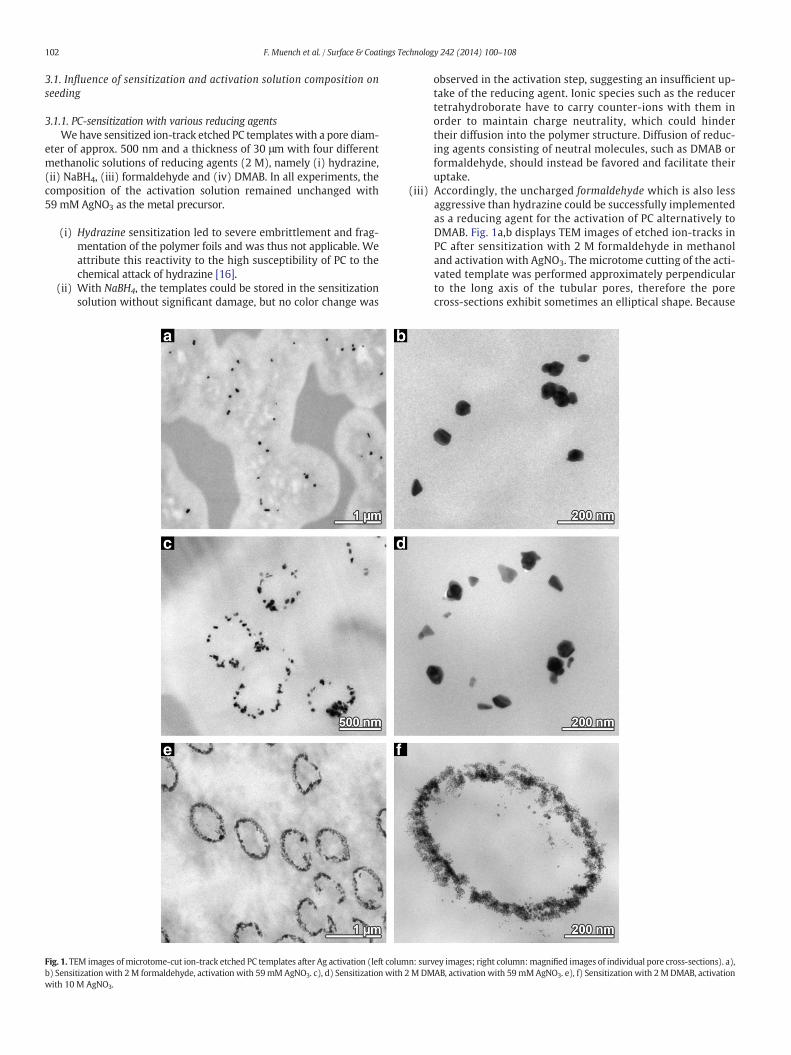
3.1.3. Influence of the DMAB sensitization solution concentrationThe DMAB concentration in the sensitization solution affects the up-
take of the reducing agent by the polymer substrate [8] and thus shouldallow modification of the amount of metal precipitated during activa-tion in a controlled manner. We investigated this issue by applyingtwo different activation solutions (59 mM AgNO3 and 59 mM K2PtCl4)on three PC templates each sensitized with a different concentrationof DMAB, namely 0.25 M, 1 M and 2 M.
The shape, size and density of the resulting seeds were studied byTEM and AFM (Fig. 2). Fig. 2a–c shows AFM images of the Ag-activated samples, in Fig. 2e–g the results for the Pt activation aredisplayed. In each row, the DMAB concentration is rising from left toright. In Fig. 2d and h, TEM images of Ag and Pt seeds obtained with 2M DMAB are found.
The AFM measurements clearly evidence that the roughness of themetallized polymer surface increases with the DMAB concentration in
Fig. 4. a), b) SEM images of Cu NTs fabricated in an ion-track etched PC template sensitized wmode) of two Ag NTs (sensitization: 2 M DMAB, activation: Pt). d) SEM image of the samplebe clearly identified by the atomic number contrast.
the sensitization solution (Fig. 2a-c, e-g). Because the root mean squareroughness of the bare PC surface is less than 1 nm even after sensitiza-tion [8], the observed structures can be related to the metal NPs depos-ited during activation. This argumentation is supported by TEM imagesof NPs created during activation (Fig. 2d,h): The particle morphologyvisualized by TEM resembles the surface structure of the correspondingAFM images.While Ag tends to form faceted, relatively large and isolat-ed NPs (Fig. 2d), Pt activation yields aggregates consisting of smallerNPs (Fig. 2h).
With the lowest DMAB concentration of 0.25 M, only few small NPswere reduced on the polymer during activation with both Ag and Pt(Fig. 2a,e). A DMAB concentration of 1 M led to a stronger uptake ofthe reducing agent by the polymer and thus enabled the formation ofa much more dense layer of metal NPs (Fig. 2b,f). Compared to Pt, Agactivation yielded a higher amount of deposited metal and larger NPsizes. With the most concentrated sensitization solution (2 M DMAB),even larger, but still mostly isolated particles were found in the case ofAg (Fig. 2c), while extended clusters were obtained with Pt activation(Fig. 2g).
3.2. Influence of the substrate activity on the electroless synthesis of metalNTs
In this section, we demonstrate that the seed metal type and seeddensity can be utilized to tailor the substrate activity to affect theconsecutive electroless plating of metal NTs. We fabricated etched ion-track PC membranes with ~600 nm diameter channels, and activatedthem using DAMB, AgNO3 and PtCl4, using identical conditions to theexperiments conducted in Section 3.1.3. Thus we obtained both Agand Pt seeds with three different NP loadings. After activation, all tem-plates were subjected to electroless Ag plating for 20 h.
ith 1 M DMAB and activated with Pt seeds. c) Magnified SEM image (secondary electronshown in c) (backscattered electron mode). The Pt seeds on the outer Ag NT surface can

106 F. Muench et al. / Surface & Coatings Technology 242 (2014) 100–108
Fig. 3 shows Ag nanostructures obtained sensitization with 0.25DMAB in the case of a) Ag and b) Pt seeds. In both cases no continuousAgNTswere obtained due to the low density of seeds created during ac-tivation (see Fig. 2a,e). However, relatively dense Ag surface films wereformed on the outer, planar surfaces of the template foil. This result is inagreement with previous reports [5,19,20], corroborating that the for-mation of 2D films is easier than the homogeneous coverage of extend-ed inner surfaces poorly accessible to the reactants.
Fig. 3c,e presents free-standing AgNTs spanning the complete thick-ness of the template (~30 μm). These tubes are obtained when a higherdensity of Ag seeds is created by sensitization with more concentratedDMAB solutions, namely 1 M and 2 M.
Fig. 3d,f presents Ag nanostructures obtained with increased seeddensity in the case of Pt-seeded experiments. In these cases, onlyshort NTs are formed adjacent to the planar Ag film on the outer tem-plate surface. To exclude the possibility that an inhomogeneous seed
Fig. 5. Characterization of themetal films plated on different polymers after sensitizationwith Detched PET. c) SEM image of the Ag film deposited on ABS foil. d) Photograph of a Lego® brick acase of Ag films roughened on the nanoscale [5,29]. e), f) SEM images of the Au film deposited oreferred to the web version of this article.)
distribution with low particle densities within the template channelswas responsible for this result, we performed electroless Cu plating onan ion-track etched membrane activated with Pt seeds after sensitiza-tion with 1 M DMAB. Fig. 4a,b evidences the formation of well-definedCu NTs. Because an identical amount and distribution of seeds did notsuffice to enable the formation of extended free-standing Ag NTs(Fig. 3d), the Pt NPs initiatedmetal film nucleationmore reliably withinthe depth of the template pores when comparing Cu with Ag plating.This result points out that the activation parameters of the substratesused in the electroless fabrication of nanomaterials must be optimizedwith respect to the applied plating solution.
We found that in the case of the employed electroless Ag plating re-action, Pt seeding led to less Ag deposition within the template com-pared to Ag seeding under identical plating conditions (Fig. 3). Thisindicates a slower formation of the Ag film in the Pt-activated template,which can be explained by a reduced activity of the Pt seeds in the
MAB and activationwith Ag. a), b) SEM images of the nanostructured Ag film on ion-trackfter electroless Ag plating. The light golden color of thework piece is often observed in then PVA foil. (For interpretation of the references to color in this figure legend, the reader is

107F. Muench et al. / Surface & Coatings Technology 242 (2014) 100–108
plating reaction. Ideally, metal deposition should occur faster on theseed particles than on the plated metal film, because in this casesubstrate areas where film nucleation has not started yet are preferreddeposition sites [21]. Due to their improved activity compared to thePt seeds, Ag seeds are therefore preferred to obtain free-standing AgNTs of high aspect ratio in the reaction conditions described here.
Despite the fact that no continuous Ag NTs were obtained in the Ptactivation experiments (Fig. 3b,d,f), it is important to note that theoutlined reaction scheme can be used to create metal NTs decoratedwith NPs on their outerwalls consisting of a secondmetal (Fig. 4c,d). Bi-nary NTs represent an upcoming catalyst system benefiting from both aunique morphology and synergistic effects [22,23], thus activation witha seed metal differing from the NT material is an interesting andstraightforward route towards metal NTs with improved functionality.
3.3. Activation protocol for different polymers
In the study introducing the swelling activation technique [8], PCwas used because of its privileged role as a template for the depositionof high aspect ratio nanomaterials such as nanowires [24] and NTs [7].To prove the universality of the activation scheme, it is now shownhow the process can be transferred to other polymers. Three polymertypes with significantly deviating properties were chosen, namely(i) PET, (ii) ABS and (iii) PVA. For all three polymers, we used technicalpolymer data sheets, and it was of high importance to choose a sensiti-zation solvent which causes slight swelling of the substrate surfacewithout damaging themorphology of thework piece or even dissolve it.
(i) PET is a polyester like PC, but is characterized by a higher chem-ical stability and thus can be applied under more aggressive con-ditions [25]. Given the stability of PET in methanol, 1,4-dioxanewas chosen as solvent for the sensitization of PET membranes.Using DMAB as the reducing agent, Ag nuclei were deposited inthe activation step, followed by electroless Ag plating. Duringactivation, the PET template turned brownish, indicating the cre-ation of Ag seeds. After electroless plating, a metallic gray lusterappeared. The creation of a homogeneous thin film composedof the relatively large NPs typical for electroless Ag [5] was con-firmed by SEM (Fig. 5a,b). The porous structure of the templatewas fully preserved during the treatment (Fig. 5a,b). As can beseen in Fig. 5b, Ag deposition also took place on the inner surfacesof the PET substrate.
(ii) ABS is an industrially important polymer frequently used for elec-troless plating [1,26]. Due to its hydrophobic nature, etching andoxidizing steps are usually required to provide adhesion for plat-ed metal films and to introduce polar surface functionalities foractivation procedures [26,27]. The sensitization procedure usedfor PC could directly be transferred to ABS. After being sensitizedin a methanolic solution of DMAB, activation in an aqueous solu-tion of AgNO3 yielded intensely brown-colored ABS substrateswhich could be evenlymetallized by consecutive electroless plat-ing (Fig. 5c,d). Dense Ag films were obtained, as expected fromthe high seed loading indicated by the strong color shift duringactivation [7]. The presence of a nanostructured Ag filmwas con-firmed with SEM (Fig. 5c). Both home-made ABS foils (Fig. 5c)and complex shaped, macroscopic work pieces such as Lego®bricks (Fig. 5d) were successfully plated.
(iii) PVA is an extremely hydrophilic and biocompatible polymer [28].The home-made PVA foils used for the experiments were watersoluble. Thus, all reaction steps (sensitization, activation, electro-less plating) were performed in non-aqueous solvents. WhileDMAB sensitizationwas performedwithmethanol, ethylene gly-col was used for activation because of its improved solubility ofinorganic salts such as the AgNO3 used as metal source. After ac-tivation, the brownish PVA foilswere placed in an ethylene glycolbased electroless Au plating bath. During the storage of the
polymer foil in the reaction solution, a color shift to blue wasobserved in addition with a slight bronze-colored luster. SEMmeasurements confirmed the presence of a porous nanoscaleAu film (Fig. 5e,f).
In all shown experiments, metal film adhesionwhich displays an es-sential issue in electroless plating [1,26] was unproblematic. No delam-ination of the metal films was observed after plating as well as duringscotch tape tests. This is expected in the case of the ion-track etchedPC and PET templates, since the polymer foils contain a high density ofpores which reliably anchor themetal films on their surfaces. Consider-ing the ABS substrates, a certain roughness was found after swellingactivation and plating (see Fig. 5c), which is probably the cause for thegood metal film adhesion. The bonding of the Au film to the PVA foilprobably benefited from its nanoscale structure, because it is wellknown that ensuring metal adhesion is especially challenging for largefilm thicknesses [1]. Consequently, in syntheses using extended platingtimes and smooth PC foils not containing pores from ion-track etching,we frequently observed metal film peeling. This is not surprising, sincethe applied reaction conditions do not increase the surface roughnessof the utilized PC foils significantly [8], which is necessary to improvemechanical bonding due to the otherwise mostly weak interactions be-tweenmetals and polymers [1,26,27,30]. While the conservation of finemorphological features is important for template-based nanomaterialfabrication, in such cases, surface-roughening pretreatments [1,30] arerequired before sensitization.
4. Conclusion
In this study, the activation of polymer substrates sensitized by theabsorption of reducing agents in the presence of swelling solvents wasdemonstrated to be a universal and highly flexible process. By choosingappropriate solvents causing a controlled modification of the polymersurface without destroying the substrate morphology, four polymerswith strongly differing chemical structures were successfully activatedfor consecutive electroless plating. Also, the reducing agent and seedmetal could be varied.
The reaction conditions during sensitization and activation stronglyaffected the formation of metal NPs. Highmetal loadings were obtainedby sensitization with concentrated solutions of the strong reducingagent DMAB. The seed particle shape, size and distribution dependedon the composition of both the sensitization and activation solutions,with a particularly pronounced impact of the metal precursor type.
Because the activation quality is of major relevance for the electro-less synthesis of metal thin films and nanomaterials derived thereof,the effect of the seeding parameters on the fabrication of free-standing metal NTs was evaluated. To achieve this challenging prod-uct morphology, an appropriate seed loading proved to be necessary,but not sufficient. Generally, an adequate density of seeds which areactive in the corresponding plating reaction and ensure reliablenucleation is required to homogeneously cover complex shaped sub-strates with nanoscale metal films.
Acknowledgments
We thank Prof. Dr. Christina Trautmann (GSI Helmholtzzentrum fürSchwerionenforschung GmbH (Darmstadt, Germany)) for support withthe irradiation experiments and for providing access to the HRSEM ofthe materials research group. The authors highly recognize the synthe-ses performed by Sebastian Bohn.
References
[1] G.O. Mallory, J.B. Hajdu (Eds.), Electroless Plating: Fundamentals And Applications,American Electroplaters and Surface Finishers Society, Florida/William Andrew Pub-lishing, New York, 1990.

108 F. Muench et al. / Surface & Coatings Technology 242 (2014) 100–108
[2] S. Balci, K. Hahn, P. Kopold, A. Kadri, C. Wege, K. Kern, A.M. Bittner, Nanotechnology23 (2012) 045603.
[3] F. Formanek, N. Takeyasu, T. Tanaka, K. Chiyoda, A. Ishikawa, S. Kawata, Appl. Phys.Lett. 88 (2006) 083110.
[4] M. Wirtz, S. Yu, C.R. Martin, Analyst 127 (2002) 871–879.[5] F. Muench,M. Rauber, C. Stegmann, S. Lauterbach, U. Kunz, H.-J. Kleebe,W. Ensinger,
Nanotechnology 22 (2011) 415602.[6] C.R.K. Rao, D.C. Trivedi, Coord. Chem. Rev. 249 (2005) 613–631.[7] F. Muench, M. Oezaslan, T. Seidl, S. Lauterbach, P. Strasser, H.-J. Kleebe, W. Ensinger,
Appl. Phys. A 105 (2011) 847–854.[8] F. Muench, S. Bohn, M. Rauber, T. Seidl, A. Radetinac, U. Kunz, S. Lauterbach, H.-J.
Kleebe, C. Trautmann, W. Ensinger, Appl. Phys. A (2014), http://dx.doi.org/10.1007/s00339-013-8119-z(accepted for publication).
[9] P.P. Lau, C.C. Wong, L. Chan, Appl. Surf. Sci. 253 (2006) 2357–2361.[10] I. Halaciuga, J.I.Njagi, K. Redford, D.V. Goia, J. Colloid Interface Sci. 383 (2012) 215–221.[11] K.A.Nelson,M.R. Linford,D.R.Wheeler, J.N.Harb, Electrochim.Acta 69 (2012) 320–327.[12] D. Zabetakis, W.J. Dressick, ACS Appl. Mater. Interfaces 1 (2009) 4–25.[13] F. Basarir, ACS Appl. Mater. Interfaces 4 (2012) 1324–1329.[14] W.-P. Dow, G.-L. Liao, S.-E. Huang, S.-W. Chen, J. Mater. Chem. 20 (2010) 3600–3609.[15] J.H. Byeon, Y.-W. Kim, ACS Appl. Mater. Interfaces 3 (2011) 2912–2918.
[16] http://www.palramhort.com/pdffiles/PC_Products_General_Info/PC_Chemical_Resistance.pdf (chemical resistance of polycarbonate sheets, accessed: 04.11.2013).
[17] I. Ohno, O. Wakabayashi, S. Haruyama, J. Electrochem. Soc. 132 (1985) 2323–2330.[18] Y. Xia, Y. Xiong, B. Lim, S.E. Skrabalak, Angew. Chem. Int. Ed. 48 (2009) 60–103.[19] D.P. Wernette, C.B. Swearingen, D.M. Cropek, Y. Lu, J.V. Sweedler, P.W. Bohn, Analyst
131 (2006) 41–47.[20] L. Velleman, J.G. Shapter, D. Losic, J. Membr. Sci. 328 (2009) 121–126.[21] C.D. Iacovangelo, K.P. Zarnoch, J. Electrochem. Soc. 138 (1991) 983–988.[22] F. Muench, S. Kaserer, U. Kunz, I. Svoboda, J. Brötz, S. Lauterbach, H.-J. Kleebe, C.
Roth, W. Ensinger, J. Mater. Chem. 21 (2011) 6286–6291.[23] C. Koenigsmann, S.S. Wong, Energy Environ. Sci. 4 (2011) 1161–1176.[24] M.E. Toimil-Molares, Beilstein J. Nanotechnol. 3 (2012) 860–863.[25] F. Muench, C. Neetzel, S. Kaserer, J. Brötz, J.-C. Jaud, Z. Zhao-Karger, S. Lauterbach,
H.-J. Kleebe, C. Roth, W. Ensinger, J. Mater. Chem. 22 (2012) 12784–12791.[26] I.A. Abu-Isa, Polym.-Plast. Technol. Eng. 2 (1973) 29–65.[27] X. Tang, J. Wang, C. Wang, B. Sheng, Surf. Coat. Technol. 206 (2011) 1382–1388.[28] J. Martin, M. Martin-Gonzalez, A. del Campo, J.J. Reinosa, J.F. Fernandez, Nanotech-
nology 23 (2012) 385305.[29] H. He, W. Cai, Y. Lin, Z. Dai, Langmuir 27 (2011) 1551–1555.[30] D. Schröer, R.J. Nicholst, H. Meyer, Electrochim. Acta 40 (1995) 1487–1494.