GL3233
USB 3.0 Single-LUN
Memory Card Reader Controller
Datasheet
Revision 1.02 Nov. 07, 2012
Genesys Logic, Inc.
GL3233 Datasheet
©2012 Genesys Logic, Inc. - All rights reserved. Page 2
Copyright Copyright © 2012 Genesys Logic, Inc. All rights reserved. No part of the materials shall be reproduced in any form or by any means without prior written consent of Genesys Logic, Inc.
Ownership and Title Genesys Logic, Inc. owns and retains of its right, title and interest in and to all materials provided herein. Genesys Logic, Inc. reserves all rights, including, but not limited to, all patent rights, trademarks, copyrights and any other propriety rights. No license is granted hereunder.
Disclaimer
All Materials are provided “as is”. Genesys Logic, Inc. makes no warranties, express, implied or otherwise, regarding their accuracy, merchantability, fitness for any particular purpose, and non-infringement of intellectual property. In no event shall Genesys Logic, Inc. be liable for any damages, including, without limitation, any direct, indirect, consequential, or incidental damages. The materials may contain errors or omissions. Genesys Logic, Inc. may make changes to the materials or to the products described herein at anytime without notice.
Genesys Logic, Inc. 12F., No. 205, Sec. 3, Beixin Rd., Xindian Dist. 231,
New Taipei City, Taiwan
Tel : (886-2) 8913-1888
Fax : (886-2) 6629-6168
http ://www.genesyslogic.com
GL3233 Datasheet
©2012 Genesys Logic, Inc. - All rights reserved. Page 3
Revision History
Revision Date Description
1.00 05/10/2012 First Formal Release
1.01 07/30/2012
1. Adding WHQL/WHCK Submission ID, p7 2. Adding LQFP 48 Pinout Diagram/Description, p7, 10, 15, 16 3. Adding LQFP 48 Package dimension, p25 4. Adding part number-GL3233-MNYXX in Chapter 8 ordering information, p26 5. Update SPI Flash support list in Chapter 6, p22 6. Adding top marking information in Chapter 7, p23, 24
1.02 11/07/2012 1. Update SPI Flash support list in Chapter 6, p22
GL3233 Datasheet
©2012 Genesys Logic, Inc. - All rights reserved. Page 4
Table of Contents
CHAPTER 1 GENERAL DESCRIPTION........................................................................ 6
CHAPTER 2 FEATURES................................................................................................... 7
CHAPTER 3 PIN ASSIGNMENT...................................................................................... 8
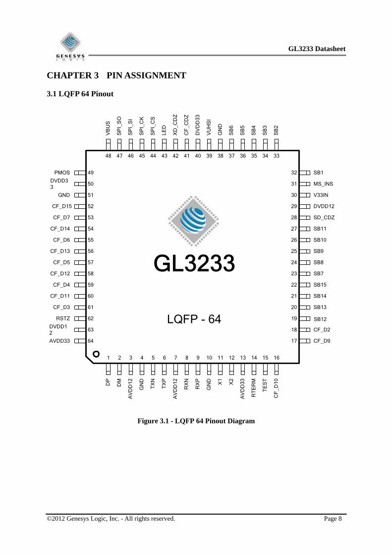
3.1 LQFP 64 Pinout ............................................................................................................ 8
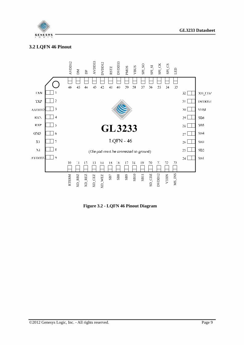
3.2 LQFN 46 Pinout............................................................................................................ 9
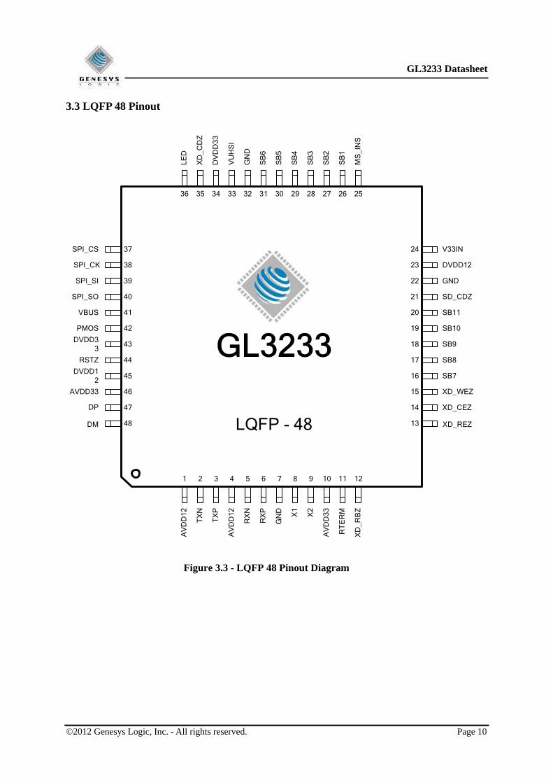
3.3 LQFP 48 Pinout .......................................................................................................... 10
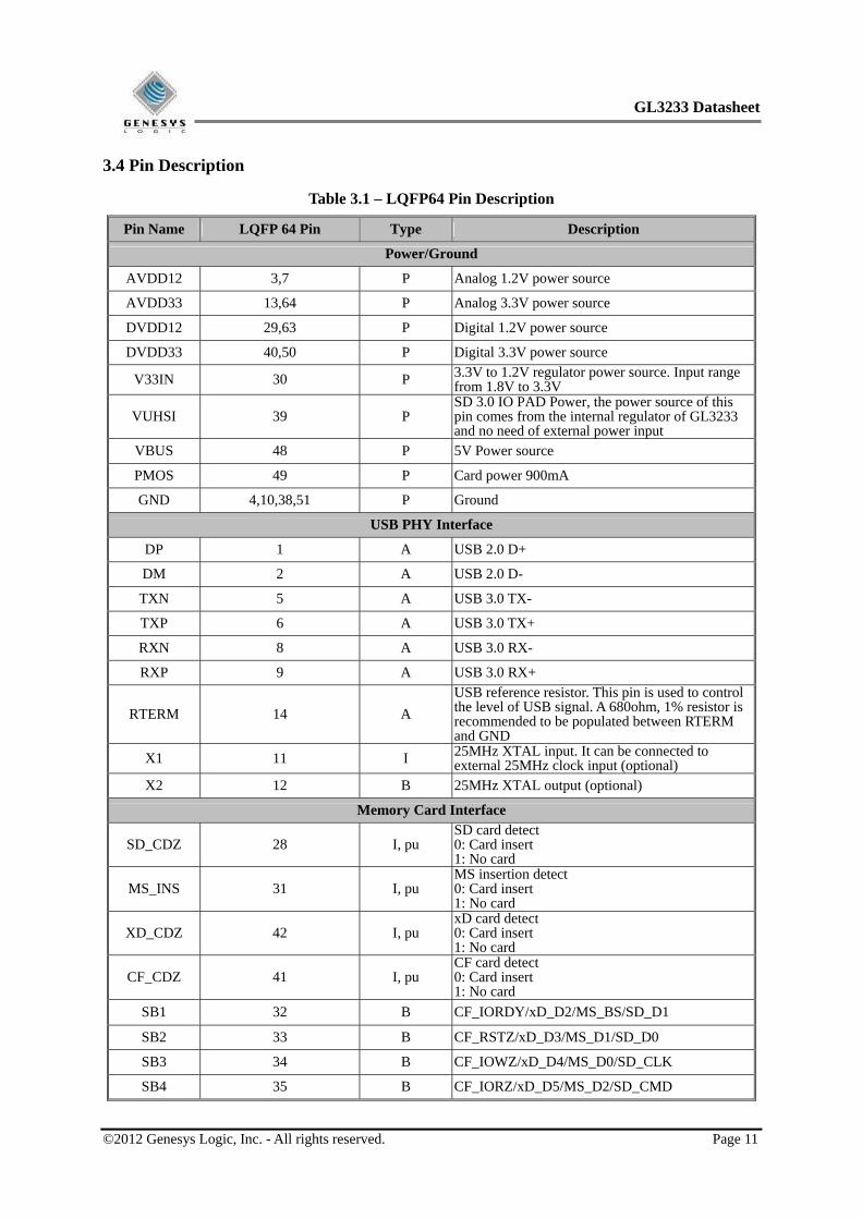
3.4 Pin Description ........................................................................................................... 11
CHAPTER 4 BLOCK DIAGRAM................................................................................... 17
4.1 Super Speed and HS/FS PHY.................................................................................... 17
4.2 USB Controller ........................................................................................................... 17
4.3 EPFIFO ....................................................................................................................... 17
4.4 MCU ............................................................................................................................ 17
4.5 MHE (Media Hardware Engine) .............................................................................. 18
4.6 Regulator ..................................................................................................................... 18
CHAPTER 5 ELECTRICAL CHARACTERISTICS.................................................... 19
5.1 Temperature Conditions............................................................................................ 19
5.2 Operating Conditions................................................................................................. 19
5.3 DC Characteristics ..................................................................................................... 19
5.4 AC Characteristics of Reset Timing ......................................................................... 20
CHAPTER 6 SPI NOR FLASH SUPPORT LIST .......................................................... 22
CHAPTER 7 PACKAGE DIMENSION.......................................................................... 23
CHAPTER 8 ORDERING INFORMATION.................................................................. 26
GL3233 Datasheet
©2012 Genesys Logic, Inc. - All rights reserved. Page 5
List of Figures
Figure 3.1 - LQFP 64 Pinout Diagram ................................................................................... 8
Figure 3.2 - LQFN 46 Pinout Diagram................................................................................... 9
Figure 3.3 - LQFP 48 Pinout Diagram ................................................................................. 10
Figure 4.1 - Functional Block Diagram................................................................................ 17
Figure 5.2 - Timing Diagram of Power Good to USB Command Receive Ready ............ 20
Figure 7.1 - LQFP 64 Pin Package........................................................................................ 23
Figure 7.2 - LQFN 46 Pin Package ....................................................................................... 24
Figure 7.3 - LQFP 48 Pin Package........................................................................................ 25
List of Tables
Table 3.1 – LQFP64 Pin Description.................................................................................... 11
Table 3.2 – LQFN46 Pin Description ................................................................................... 13
Table 3.3 – LQFP48 Pin Description.................................................................................... 15
Table 5.1 - Temperature Conditions .................................................................................... 19
Table 5.2 - Operating Conditions.......................................................................................... 19
Table 5.3 - DC Characteristics .............................................................................................. 19
Table 5.4 - Reset Timing ........................................................................................................ 21
Table 5.5 - SD/MMC Card Clock Frequency ...................................................................... 21
Table 5.6 - MS Card Clock Frequency................................................................................. 21
Table 6.1 - SPI NOR Flash Support List.............................................................................. 22
Table 8.1 - Ordering Information......................................................................................... 26
GL3233 Datasheet
©2012 Genesys Logic, Inc. - All rights reserved. Page 6
CHAPTER 1 GENERAL DESCRIPTION
GL3233 is a crystal-less USB 3.0 Single-LUN card reader controller which can support various types of memory cards, such as CompactFlashTM, Secure DigitalTM (SD), SDHC, miniSD, microSD (T-Flash), MultiMediaCardTM (MMC), RS-MMC, MMCmicro, MMCmobile, Memory StickTM (MS), Memory Stick DuoTM (MS Duo), High Speed Memory StickTM (HS MS), Memory Stick PROTM (MS PRO), Memory Stick PROTM Duo (MS PRO Duo), Memory Stick PRO-HGTM (MS PRO-HG), MS PRO Micro and xD-Picture CardTM on one chip. It also supports SDXC and Memory Stick XC high density memory cards (capacity up to 2TB) and high speed SD3.0 UHS-I memory cards. The GL3233 integrates a high speed 8051 microprocessor and a high efficiency hardware engine for the best data transfer performance between USB and various memory card interfaces. It supports ISP (In System Programming) for firmware upgrade into the external SPI Flash via USB port. It also integrates 5V to 3.3V and 3.3V to 1.2V regulators and power MOSFETs which can reduce the system BOM cost.
GL3233 Datasheet
©2012 Genesys Logic, Inc. - All rights reserved. Page 7
CHAPTER 2 FEATURES
USB specification compliance
- Comply with Universal Serial Bus 3.0 Specification rev. 1.0 (USB 3.0) - Comply with Universal Serial Bus Specification rev. 2.0 (USB 2.0) - Comply with USB Mass Storage Class Specification rev. 1.0 - Support USB Mass Storage Class Bulk-Only Transport (BOT) - Support 1 device address and up to 3 endpoints: Control (0) / Bulk Data Write Out (1) / Bulk Data
Read In (2) - Support 5 Gbps/SuperSpeed, 480 Mbps/high-speed, and 12 Mbps/full-speed transfer rates
Integrated USB building blocks
- SuperSpeed/USB2.0 transceiver macro (UTM), Serial Interface Engine (SIE) and embedded Power-On Reset (POR)
Embedded high speed 8051 micro-controller
High efficiency hardware DMA engine improves data transfer performance between USB and flash card
interfaces
Support CompactFlashTM v6.0 with PIO mode 6 / Ultra DMA mode 7 and LBA48 (Capacity up to 144PB)
Support Secure DigitalTM v1.0 / v1.1 / v2.0/ SDHC / SDXC (capacity up to 2TB)
Support Secure DigitalTM v3.0 UHS-I (Ultra High Speed): SDR12/SDR25/SDR50/DDR50/SDR104
Compliant with MultiMediaCardTM (MMC)
- MMC specification v3.x / v4.0 / v4.1 / v4.2 / v4.3 / v4.4 - x1 / x4 / x8 bit data bus
Support Memory StickTM / Memory Stick PRO / Memory Stick PRO Duo / Memory Stick Micro /Memory Stick PRO-HG / Memory Stick XC (capacity up to 2TB) - Compliant with Memory Stick Series Specification: MS v1.43, MS PRO v1.05, MS Micro v1.04 (MS
HG Micro v1.00), MS PRO-HG Duo 1.03, MS XC Duo v1.00, MS XC-HG Duo v1.00, MS XC Micro v1.00 and MS XC-HG Micro v1.00
- Support Read/Write quad data access (512Bytex4) for MS PRO-HG to enhance the transmission rate
Support xD-Picture CardTM v1.2C Type M/H
Support ISP (In System Programming) for firmware upgrade into the external SPI Flash via USB port
On-Chip power MOSFETs for supplying flash media card power
On-chip 5V to 3.3V and 3.3V to 1.2V regulator
Support U0/U1/U2/U3 power management mode
Support OCCS (On-Chip Clock Source) to eliminate the use of external 25MHz crystal
Pass the USB-IF Test Procedure for SuperSpeed product (TID: 340810011)
Pass WHCK (Windows Hardware Certification Kit) test for Windows 8 (Submission ID: 1508144)
Pass WHQL (Windows Hardware Quality Lab) test for Windows 7 (Submission ID: 1497856)
Available in LQFP64 pin package (7x7mm) which can support one LUN: SD/MS/xD/CF
Available in LQFN46 pin package (6.5x4.5mm) which can support one LUN: SD/MS/xD
Available in LQFP48 pin package (7x7mm) which can support one LUN: SD/MS/xD
GL3233 Datasheet
©2012 Genesys Logic, Inc. - All rights reserved. Page 8
CHAPTER 3 PIN ASSIGNMENT
3.1 LQFP 64 Pinout
LQFP - 64
57
58
59
60
61
62
63
64
49
50
51
52
53
54
55
56 25
24
23
22
21
20
19
18
17
32
31
30
29
28
27
26
6 7 8 9 10 11 12 13 14 15 1654321
43 42 41 40 39 38 37 36 35 34 334445464748
CF_D5
CF_D12
CF_D4
CF_D11
CF_D3
RSTZ
DVDD12
AVDD33
PMOS
DVDD33
GND
CF_D15
CF_D7
CF_D14
CF_D6
CF_D13
X1
GN
D
RX
P
RX
N
AV
DD
12
TX
P
TX
N
GN
D
AV
DD
12DMDP X2
AV
DD
33
RT
ER
M
TE
ST
CF
_D10
SB8
SB7
SB15
SB14
SB13
SB12
CF_D2
CF_D9
SB1
MS_INS
V33IN
DVDD12
SD_CDZ
SB11
SB10
SB9
GN
D
VU
HS
I
DV
DD
33
CF
_CD
Z
XD
_CD
Z
LED
SP
I_C
S
SP
I_C
K
SP
I_S
I
SP
I_S
O
VB
US
SB
6
SB
5
SB
4
SB
3
SB
2
Figure 3.1 - LQFP 64 Pinout Diagram
GL3233 Datasheet
©2012 Genesys Logic, Inc. - All rights reserved. Page 9
3.2 LQFN 46 Pinout
SD
_CD
Z
XD
_RB
Z
XD
_RE
Z
XD
_WE
Z
SB
7
SB
8
SB
9
SB
10
SB
11
V33
IN
XD
_CE
Z
SP
I_C
S
SP
I_C
K
SP
I_S
O
VB
US
PM
OS
DV
DD
33
RS
TZ
DV
DD
12
AV
DD
33
DP
DM
AV
DD
12R
TE
RM
DV
DD
12
MS
_IN
SL
ED
SP
I_S
I
Figure 3.2 - LQFN 46 Pinout Diagram
GL3233 Datasheet
©2012 Genesys Logic, Inc. - All rights reserved. Page 10
3.3 LQFP 48 Pinout
LQFP - 48
43
44
45
46
47
48
37
38
39
40
41
42 19
18
17
16
15
14
13
24
23
22
21
20
4 5 6 7 8 9 10 11 12321
33 32 31 30 29 28 27 26 25343536
DVDD33
RSTZ
DVDD12
AVDD33
DP
DM
SPI_CS
SPI_CK
SPI_SI
SPI_SO
VBUS
PMOS
X2
X1
GN
D
RX
P
RX
N
AV
DD
12
TX
P
TX
N
AV
DD
12
AV
DD
33
RT
ER
M
XD
_RB
Z
SB9
SB8
SB7
XD_WEZ
XD_CEZ
XD_REZ
V33IN
DVDD12
GND
SD_CDZ
SB11
SB10
SB
3
SB
4
SB
5
SB
6
GN
D
VU
HS
I
DV
DD
33
XD
_CD
Z
LED
SB
2
SB
1
MS
_IN
S
Figure 3.3 - LQFP 48 Pinout Diagram
GL3233 Datasheet
©2012 Genesys Logic, Inc. - All rights reserved. Page 11
3.4 Pin Description
Table 3.1 – LQFP64 Pin Description
Pin Name LQFP 64 Pin Type Description
Power/Ground
AVDD12 3,7 P Analog 1.2V power source
AVDD33 13,64 P Analog 3.3V power source
DVDD12 29,63 P Digital 1.2V power source
DVDD33 40,50 P Digital 3.3V power source
V33IN 30 P 3.3V to 1.2V regulator power source. Input range from 1.8V to 3.3V
VUHSI 39 P SD 3.0 IO PAD Power, the power source of this pin comes from the internal regulator of GL3233 and no need of external power input
VBUS 48 P 5V Power source
PMOS 49 P Card power 900mA
GND 4,10,38,51 P Ground
USB PHY Interface
DP 1 A USB 2.0 D+
DM 2 A USB 2.0 D-
TXN 5 A USB 3.0 TX-
TXP 6 A USB 3.0 TX+
RXN 8 A USB 3.0 RX-
RXP 9 A USB 3.0 RX+
RTERM 14 A
USB reference resistor. This pin is used to control the level of USB signal. A 680ohm, 1% resistor is recommended to be populated between RTERM and GND
X1 11 I 25MHz XTAL input. It can be connected to external 25MHz clock input (optional)
X2 12 B 25MHz XTAL output (optional)
Memory Card Interface
SD_CDZ 28 I, pu SD card detect 0: Card insert 1: No card
MS_INS 31 I, pu MS insertion detect 0: Card insert 1: No card
XD_CDZ 42 I, pu xD card detect 0: Card insert 1: No card
CF_CDZ 41 I, pu CF card detect 0: Card insert 1: No card
SB1 32 B CF_IORDY/xD_D2/MS_BS/SD_D1
SB2 33 B CF_RSTZ/xD_D3/MS_D1/SD_D0
SB3 34 B CF_IOWZ/xD_D4/MS_D0/SD_CLK
SB4 35 B CF_IORZ/xD_D5/MS_D2/SD_CMD
GL3233 Datasheet
©2012 Genesys Logic, Inc. - All rights reserved. Page 12
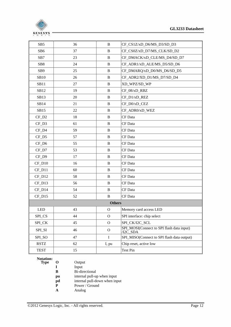
SB5 36 B CF_CS1Z/xD_D6/MS_D3/SD_D3
SB6 37 B CF_CS0Z/xD_D7/MS_CLK/SD_D2
SB7 23 B CF_DMACK/xD_CLE/MS_D4/SD_D7
SB8 24 B CF_ADR1/xD_ALE/MS_D5/SD_D6
SB9 25 B CF_DMARQ/xD_D0/MS_D6/SD_D5
SB10 26 B CF_ADR2/XD_D1/MS_D7/SD_D4
SB11 27 B XD_WPZ/SD_WP
SB12 19 B CF_08/xD_RBZ
SB13 20 B CF_D1/xD_REZ
SB14 21 B CF_D0/xD_CEZ
SB15 22 B CF_ADR0/xD_WEZ
CF_D2 18 B CF Data
CF_D3 61 B CF Data
CF_D4 59 B CF Data
CF_D5 57 B CF Data
CF_D6 55 B CF Data
CF_D7 53 B CF Data
CF_D9 17 B CF Data
CF_D10 16 B CF Data
CF_D11 60 B CF Data
CF_D12 58 B CF Data
CF_D13 56 B CF Data
CF_D14 54 B CF Data
CF_D15 52 B CF Data
Others
LED 43 O Memory card access LED
SPI_CS 44 O SPI interface: chip select
SPI_CK 45 O SPI_CK/I2C_SCL
SPI_SI 46 O SPI_MOSI(Connect to SPI flash data input) /I2C_SDA
SPI_SO 47 I SPI_MISO(Connect to SPI flash data output)
RSTZ 62 I, pu Chip reset, active low
TEST 15 Test Pin Notation:
Type O Output I Input B Bi-directional pu internal pull-up when input pd internal pull-down when input P Power / Ground A Analog
GL3233 Datasheet
©2012 Genesys Logic, Inc. - All rights reserved. Page 13
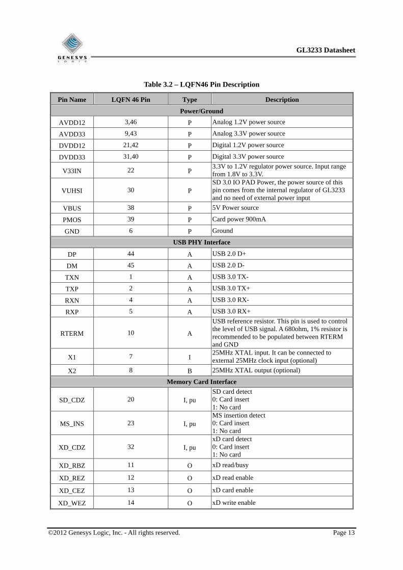
Table 3.2 – LQFN46 Pin Description
Pin Name LQFN 46 Pin Type Description
Power/Ground
AVDD12 3,46 P Analog 1.2V power source
AVDD33 9,43 P Analog 3.3V power source
DVDD12 21,42 P Digital 1.2V power source
DVDD33 31,40 P Digital 3.3V power source
V33IN 22 P 3.3V to 1.2V regulator power source. Input range from 1.8V to 3.3V.
VUHSI 30 P SD 3.0 IO PAD Power, the power source of this pin comes from the internal regulator of GL3233 and no need of external power input
VBUS 38 P 5V Power source
PMOS 39 P Card power 900mA
GND 6 P Ground
USB PHY Interface
DP 44 A USB 2.0 D+
DM 45 A USB 2.0 D-
TXN 1 A USB 3.0 TX-
TXP 2 A USB 3.0 TX+
RXN 4 A USB 3.0 RX-
RXP 5 A USB 3.0 RX+
RTERM 10 A
USB reference resistor. This pin is used to control the level of USB signal. A 680ohm, 1% resistor is recommended to be populated between RTERM and GND
X1 7 I 25MHz XTAL input. It can be connected to external 25MHz clock input (optional)
X2 8 B 25MHz XTAL output (optional)
Memory Card Interface
SD_CDZ 20 I, pu SD card detect 0: Card insert 1: No card
MS_INS 23 I, pu MS insertion detect 0: Card insert 1: No card
XD_CDZ 32 I, pu xD card detect 0: Card insert 1: No card
XD_RBZ 11 O xD read/busy
XD_REZ 12 O xD read enable
XD_CEZ 13 O xD card enable
XD_WEZ 14 O xD write enable
GL3233 Datasheet
©2012 Genesys Logic, Inc. - All rights reserved. Page 14
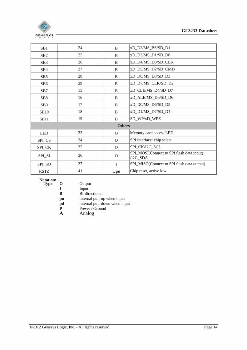
SB1 24 B xD_D2/MS_BS/SD_D1
SB2 25 B xD_D3/MS_D1/SD_D0
SB3 26 B xD_D4/MS_D0/SD_CLK
SB4 27 B xD_D5/MS_D2/SD_CMD
SB5 28 B xD_D6/MS_D3/SD_D3
SB6 29 B xD_D7/MS_CLK/SD_D2
SB7 15 B xD_CLE/MS_D4/SD_D7
SB8 16 B xD_ALE/MS_D5/SD_D6
SB9 17 B xD_D0/MS_D6/SD_D5
SB10 18 B xD_D1/MS_D7/SD_D4
SB11 19 B SD_WP/xD_WPZ
Others
LED 33 O Memory card access LED
SPI_CS 34 O SPI interface: chip select
SPI_CK 35 O SPI_CK/I2C_SCL
SPI_SI 36 O SPI_MOSI(Connect to SPI flash data input) /I2C_SDA
SPI_SO 37 I SPI_MISO(Connect to SPI flash data output)
RSTZ 41 I, pu Chip reset, active low Notation:
Type O Output I Input B Bi-directional pu internal pull-up when input pd internal pull-down when input P Power / Ground A Analog
GL3233 Datasheet
©2012 Genesys Logic, Inc. - All rights reserved. Page 15
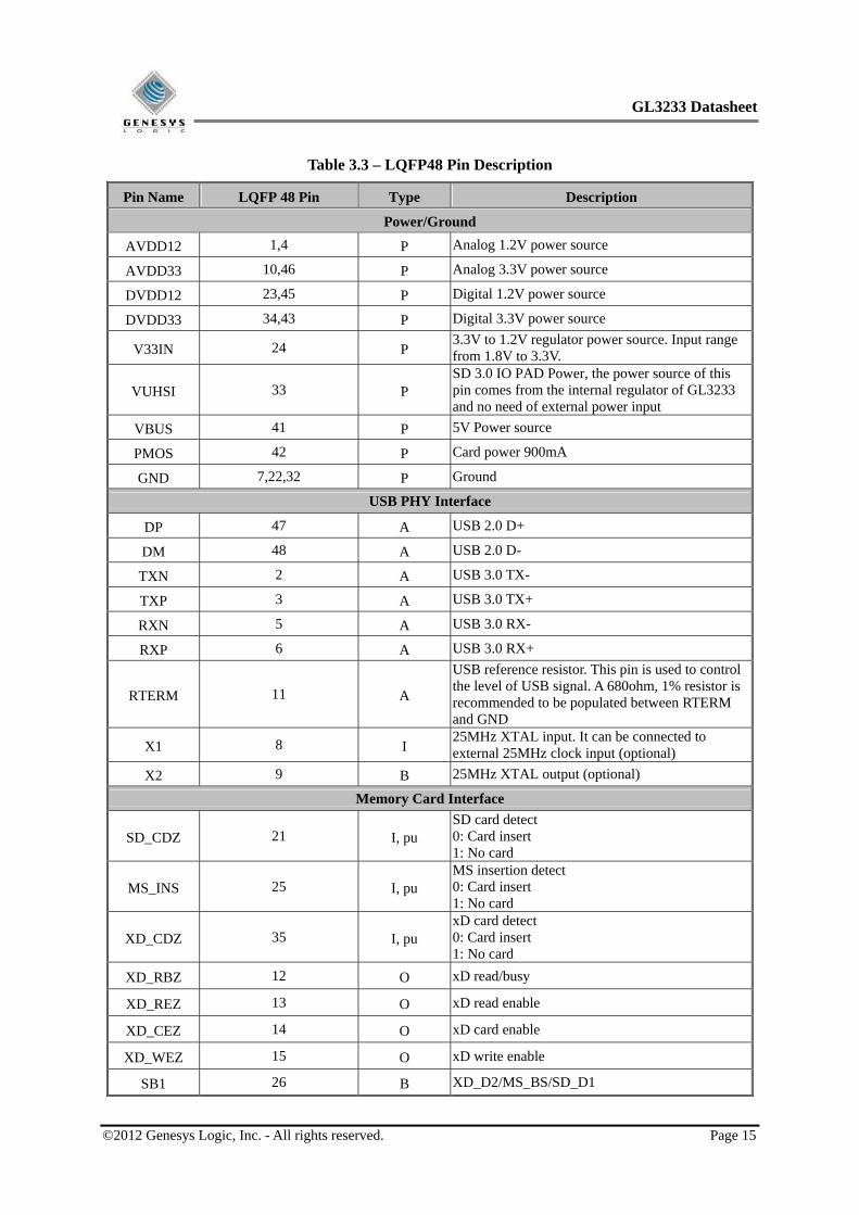
Table 3.3 – LQFP48 Pin Description
Pin Name LQFP 48 Pin Type Description
Power/Ground
AVDD12 1,4 P Analog 1.2V power source
AVDD33 10,46 P Analog 3.3V power source
DVDD12 23,45 P Digital 1.2V power source
DVDD33 34,43 P Digital 3.3V power source
V33IN 24 P 3.3V to 1.2V regulator power source. Input range from 1.8V to 3.3V.
VUHSI 33 P SD 3.0 IO PAD Power, the power source of this pin comes from the internal regulator of GL3233 and no need of external power input
VBUS 41 P 5V Power source
PMOS 42 P Card power 900mA
GND 7,22,32 P Ground
USB PHY Interface
DP 47 A USB 2.0 D+
DM 48 A USB 2.0 D-
TXN 2 A USB 3.0 TX-
TXP 3 A USB 3.0 TX+
RXN 5 A USB 3.0 RX-
RXP 6 A USB 3.0 RX+
RTERM 11 A
USB reference resistor. This pin is used to control the level of USB signal. A 680ohm, 1% resistor is recommended to be populated between RTERM and GND
X1 8 I 25MHz XTAL input. It can be connected to external 25MHz clock input (optional)
X2 9 B 25MHz XTAL output (optional)
Memory Card Interface
SD_CDZ 21 I, pu SD card detect 0: Card insert 1: No card
MS_INS 25 I, pu MS insertion detect 0: Card insert 1: No card
XD_CDZ 35 I, pu xD card detect 0: Card insert 1: No card
XD_RBZ 12 O xD read/busy
XD_REZ 13 O xD read enable
XD_CEZ 14 O xD card enable
XD_WEZ 15 O xD write enable
SB1 26 B XD_D2/MS_BS/SD_D1
GL3233 Datasheet
©2012 Genesys Logic, Inc. - All rights reserved. Page 16
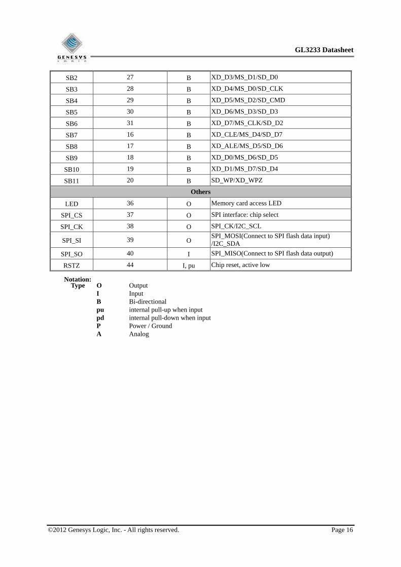
SB2 27 B XD_D3/MS_D1/SD_D0
SB3 28 B XD_D4/MS_D0/SD_CLK
SB4 29 B XD_D5/MS_D2/SD_CMD
SB5 30 B XD_D6/MS_D3/SD_D3
SB6 31 B XD_D7/MS_CLK/SD_D2
SB7 16 B XD_CLE/MS_D4/SD_D7
SB8 17 B XD_ALE/MS_D5/SD_D6
SB9 18 B XD_D0/MS_D6/SD_D5
SB10 19 B XD_D1/MS_D7/SD_D4
SB11 20 B SD_WP/XD_WPZ
Others
LED 36 O Memory card access LED
SPI_CS 37 O SPI interface: chip select
SPI_CK 38 O SPI_CK/I2C_SCL
SPI_SI 39 O SPI_MOSI(Connect to SPI flash data input) /I2C_SDA
SPI_SO 40 I SPI_MISO(Connect to SPI flash data output)
RSTZ 44 I, pu Chip reset, active low Notation:
Type O Output I Input B Bi-directional pu internal pull-up when input pd internal pull-down when input P Power / Ground A Analog
GL3233 Datasheet
©2012 Genesys Logic, Inc. - All rights reserved. Page 17
CHAPTER 4 BLOCK DIAGRAM
Figure 4.1 - Functional Block Diagram
4.1 Super Speed and HS/FS PHY
The transceiver macro is the analog circuitry that handles the low level USB protocol and signaling, and shifts the clock domain of the data from the USB to one that is compatible with the general logic.
4.2 USB Controller
The USB Controller, which contains the USB PID and address recognition logic, and other sequencing and state machine logic to handle USB packets and transactions.
4.3 EPFIFO
Endpoint FIFO includes Control FIFO (FIFO0) and Bulk In/Out FIFO
EP0 FIFO FIFO of control endpoint 0. It is 512-byte FIFO and used for endpoint 0 data transfer. Bulk In/Out FIFO It can be in the TX mode or RX mode: 1. It can be transmit/receive 512-byte data of USB 2.0 and 1K-byte data of USB 3.0 continuously. 2. It can be directly accessed by micro-controller
4.4 MCU
8051 micro-controller inside. 8051 Core Compliant with Intel 8051 high speed micro-controller ROM Firmware code on ROM
SRAM Internal RAM area for MCU access
GL3233 Datasheet
©2012 Genesys Logic, Inc. - All rights reserved. Page 18
4.5 MHE (Media Hardware Engine)
Media Interface: CF/xD/SD/MMC/MS/MS PRO/MS PRO-HG
4.6 Regulator
5V to 3.3V 3.3V Power Source 3.3V to 1.2V 1.2V Power Source
GL3233 Datasheet
©2012 Genesys Logic, Inc. - All rights reserved. Page 19
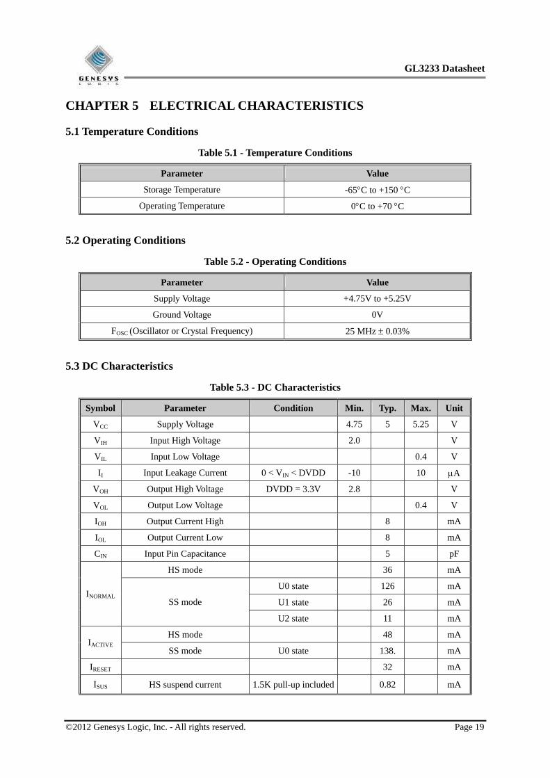
CHAPTER 5 ELECTRICAL CHARACTERISTICS
5.1 Temperature Conditions
Table 5.1 - Temperature Conditions
Parameter Value
Storage Temperature -65C to +150 C
Operating Temperature 0C to +70 C
5.2 Operating Conditions
Table 5.2 - Operating Conditions
Parameter Value
Supply Voltage +4.75V to +5.25V
Ground Voltage 0V
FOSC (Oscillator or Crystal Frequency) 25 MHz 0.03%
5.3 DC Characteristics
Table 5.3 - DC Characteristics
Symbol Parameter Condition Min. Typ. Max. Unit
VCC Supply Voltage 4.75 5 5.25 V
VIH Input High Voltage 2.0 V
VIL Input Low Voltage 0.4 V
II Input Leakage Current 0 < VIN < DVDD -10 10 A
VOH Output High Voltage DVDD = 3.3V 2.8 V
VOL Output Low Voltage 0.4 V
IOH Output Current High 8 mA
IOL Output Current Low 8 mA
CIN Input Pin Capacitance 5 pF
HS mode 36 mA
U0 state 126 mA
U1 state 26 mA INORMAL
SS mode
U2 state 11 mA
HS mode 48 mA IACTIVE
SS mode U0 state 138. mA
IRESET 32 mA
ISUS HS suspend current 1.5K pull-up included 0.82 mA
GL3233 Datasheet
©2012 Genesys Logic, Inc. - All rights reserved. Page 20
SS suspend current U3 state 0.7 mA
Reset Pad pull-up 46 KΩ
SD_CDZ, SD_WP, MS_INS, GPIO Pad pull-up
46 KΩ
SD_CMD pull-up 15 KΩRpu
SD_CLK, D[3:0] Pad pull-up 15 KΩ
RIMP SD_CMD, SD_CLK, D[3:0]
impedances 50 Ω
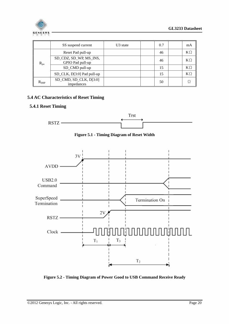
5.4 AC Characteristics of Reset Timing
5.4.1 Reset Timing
Trst
RSTZ
Figure 5.1 - Timing Diagram of Reset Width
Figure 5.2 - Timing Diagram of Power Good to USB Command Receive Ready
GL3233 Datasheet
©2012 Genesys Logic, Inc. - All rights reserved. Page 21
Table 5.4 - Reset Timing
Parameter Description Min. Unit
Trst Chip reset sense timing width 2 us
T1 AVDD power up to reset de-assert 500 us
T2 Reset de-assert to respond USB2.0 command ready 95 ms
T3 Reset de-assert to SuperSpeed termination on 12 ms
5.4.2 SD/MMC Card Clock Frequency
Table 5.5 - SD/MMC Card Clock Frequency
Parameter Description Max. Unit
FID Clock frequency Identification Mode 187 KHz
FDS Clock frequency Default Speed Mode 25 MHz
FHS SD Clock frequency High Speed Mode 50 MHz
FHS MMC Clock frequency High Speed Mode 52 MHz
FSDR25 Clock frequency Ultra High Speed Mode: SDR25 50 MHz
FDDR50 Clock frequency Ultra High Speed Mode: DDR50 50 MHz
FSDR50 Clock frequency Ultra High Speed Mode: SDR50 100 MHz
FSDR104 Clock frequency Ultra High Speed Mode: SDR104 208 MHz
5.4.3 MS Card Clock Frequency
Table 5.6 - MS Card Clock Frequency
Parameter Description Max. Unit
FDS Clock frequency Default Speed Mode 20 MHz
FMSP Clock frequency MS PRO 4bit Mode 40 MHz
FMSPHG Clock frequency MS PRO HG 8bit Mode 60 MHz
GL3233 Datasheet
©2012 Genesys Logic, Inc. - All rights reserved. Page 22
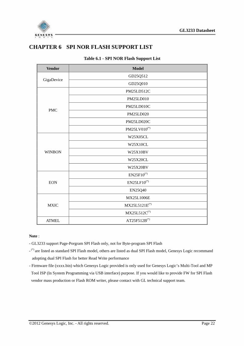
CHAPTER 6 SPI NOR FLASH SUPPORT LIST
Table 6.1 - SPI NOR Flash Support List
Vendor Model
GD25Q512 GigaDevice
GD25Q010
PM25LD512C
PM25LD010
PM25LD010C
PM25LD020
PM25LD020C
PMC
PM25LV010(*)
W25X05CL
W25X10CL
W25X10BV
W25X20CL
WINBON
W25X20BV
EN25F10(*)
EN25LF10(*) EON
EN25Q40
MX25L1006E
MX25L5121E(*) MXIC
MX25L512C(*)
ATMEL AT25F512B(*)
Note :
- GL3233 support Page-Porgram SPI Flash only, not for Byte-program SPI Flash
- (*) are listed as standard SPI Flash model, others are listed as dual SPI Flash model, Genesys Logic recommand
adopting dual SPI Flash for better Read Write performance
- Firmware file (xxxx.bin) which Genesys Logic provided is only used for Genesys Logic’s Multi-Tool and MP
Tool ISP (In System Programming via USB interface) purpose. If you would like to provide FW for SPI Flash
vendor mass production or Flash ROM writer, please contact with GL technical support team.
GL3233 Datasheet
©2012 Genesys Logic, Inc. - All rights reserved. Page 23
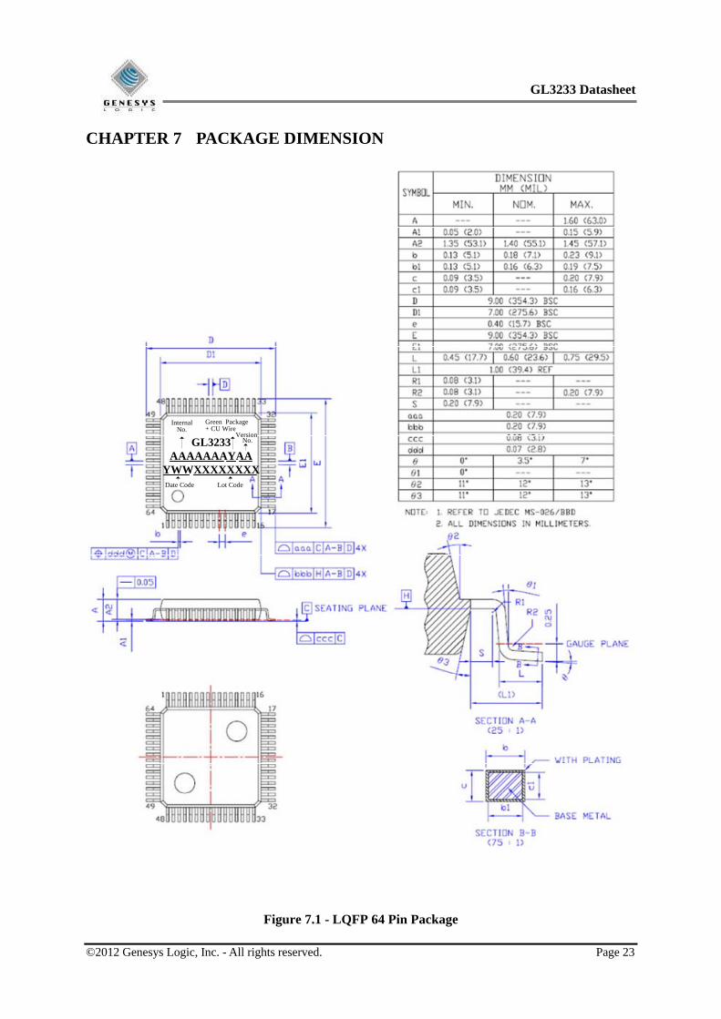
CHAPTER 7 PACKAGE DIMENSION
GL3233AAAAAAAYAA
YWWXXXXXXXXDate Code Lot Code
Internal No.
Version No.
Green Package+ CU Wire
Figure 7.1 - LQFP 64 Pin Package
GL3233 Datasheet
©2012 Genesys Logic, Inc. - All rights reserved. Page 24
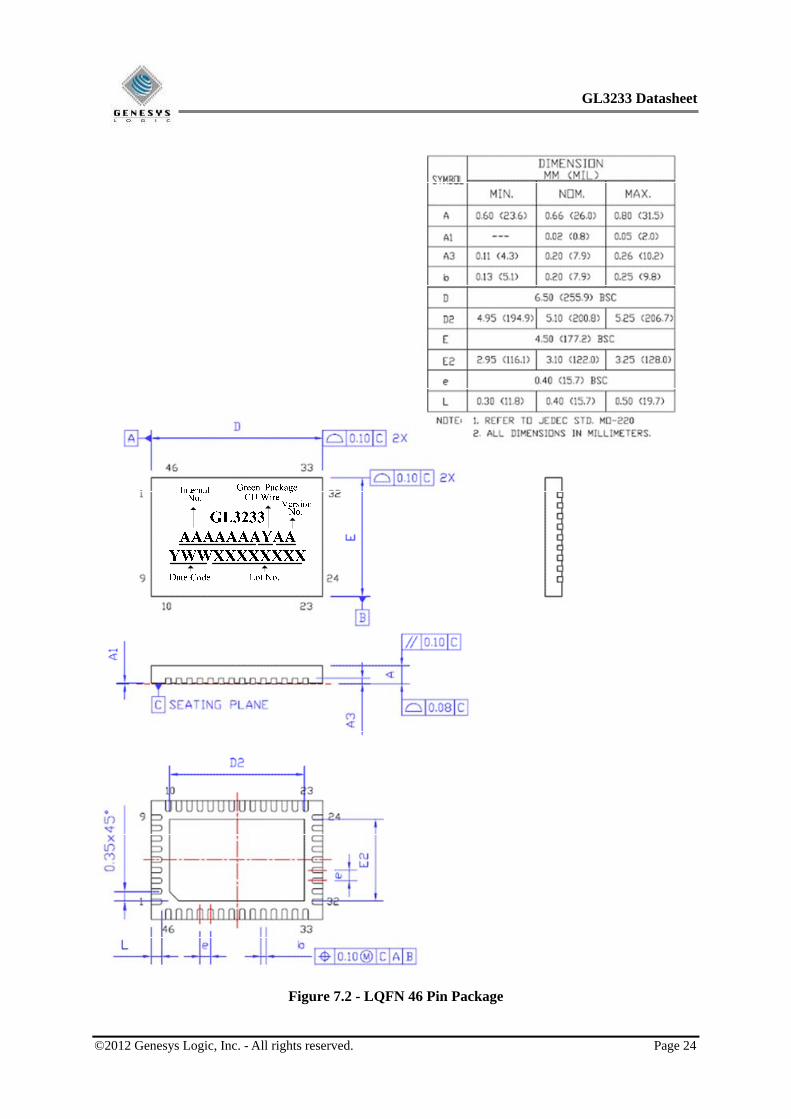
Figure 7.2 - LQFN 46 Pin Package
GL3233 Datasheet
©2012 Genesys Logic, Inc. - All rights reserved. Page 25
Date Code
Lot Code
Internal No.
Version No.
Green Package+ CU Wire
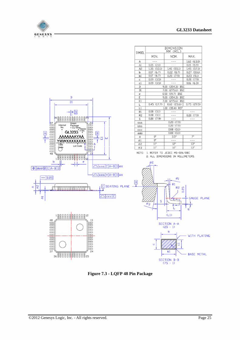
Figure 7.3 - LQFP 48 Pin Package
GL3233 Datasheet
©2012 Genesys Logic, Inc. - All rights reserved. Page 26
CHAPTER 8 ORDERING INFORMATION
Table 8.1 - Ordering Information
Part Number Package Green/Wire Material Version Status
GL3233-MSYXX LQFP 64 Green Package + CU Wire XX Available
GL3233-PMYXX LQFN 46 Green Package + CU Wire XX Available
GL3233-MNYXX LQFP 48 Green Package + CU Wire XX Available
Recommended