TOPICS IN (NANO) BIOTECHNOLOGY
Microfabrication techniques II
May 26th, 2004
PhD Course

Overview • Micromachining technologies
• Bulk micromachining• Surface Micromachining
• Basic Processes• Lithography• Wet etching• Dry etching• Deposition

Bulk, surface, DRIE

Bulk micromachining • As the name implies, bulk micromachining
focuses on the creation of patterns or features within the bulk of some sort of starting material. In doing so, we rely on the physical structure of the material in question (amnogst other variables) to control the shape of these features
• Although materials such as quartz, pyrex, GaAs, Ge, etc. Are used as teh starting material for this technology, the material that is most commonly used is silicon
• Silicon has well understood lattice structure composed of two interpenetrating face-centered-cubic (FCC) lattices

Silicon
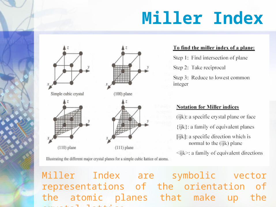
Miller Index
Miller Index are symbolic vector representations of the orientation of the atomic planes that make up the crystal lattice

Miller Index
Greater density of atoms slower etch rates

• Silicon boules are grown using a seed material of known orientation. The boule is subsequently sliced into wafers that will have this same orientation.
• Silicon etchants and silicon wafer orientations are selected to create the necessary features within the bulk of the wafer.
Silicon wafer

Bulk micromaching

Bulk micromachining

• Anisotropic etchants such as KOH:H2O (alkaline) tend to
etch different crystal planes at different rates, thus giving rise to structures having well defined sidewalls with precise and predictable angles of inclination (very little undercutting).
Anisotropic etchants
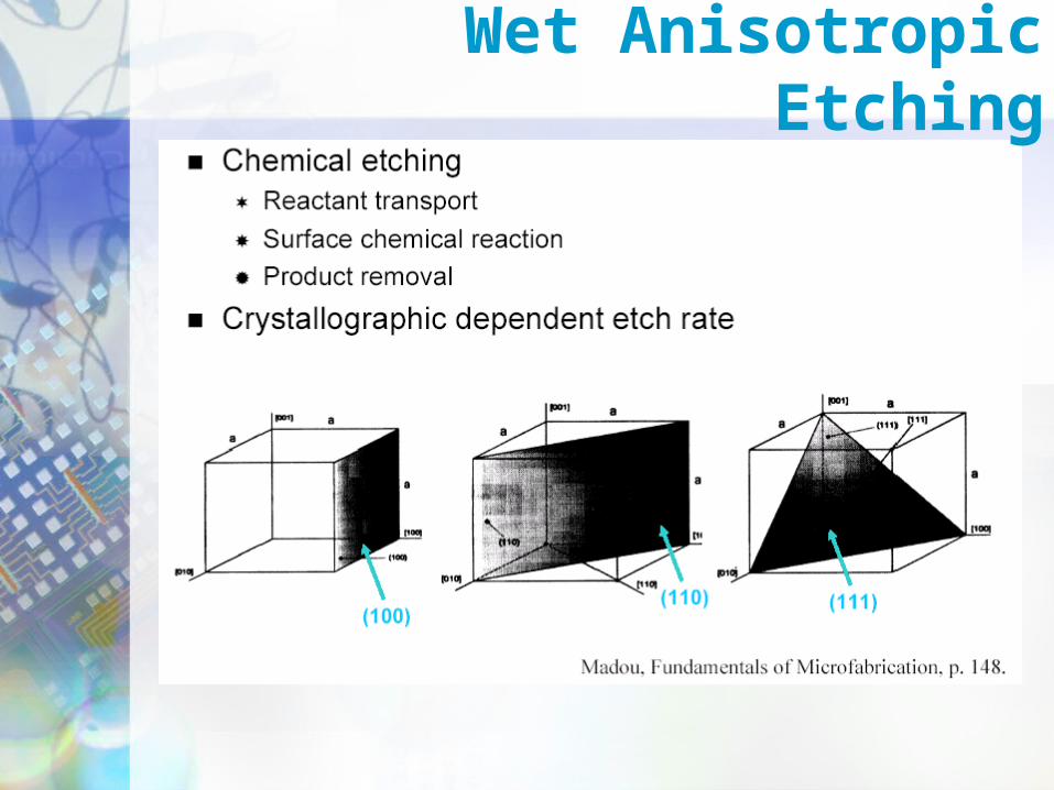
Wet Anisotropic Etching
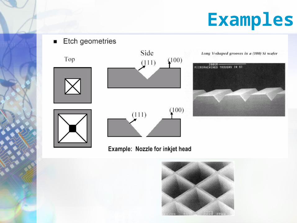
Examples

• Isotropic etchants such as mixtures of HF:HNO3:CH3COOH (acidic) tend to etch different crystal planes at the same rate, thus giving rise to rounded structures with much undercutting.
Isotropic etchants

Isotropic etchants
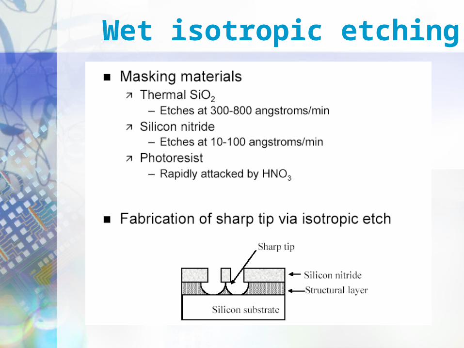
Wet isotropic etching
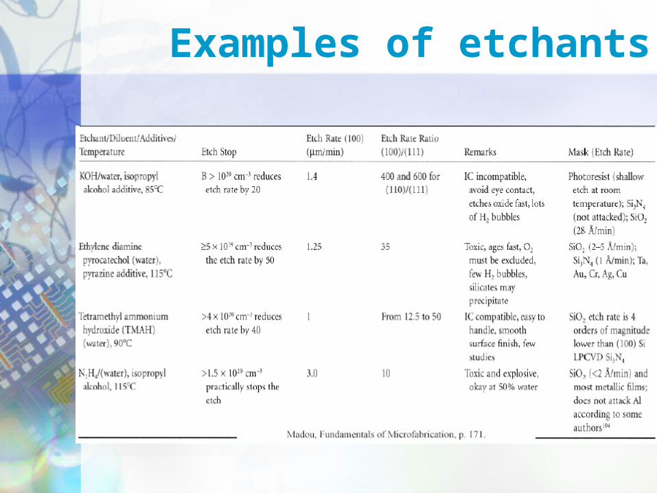
Examples of etchants
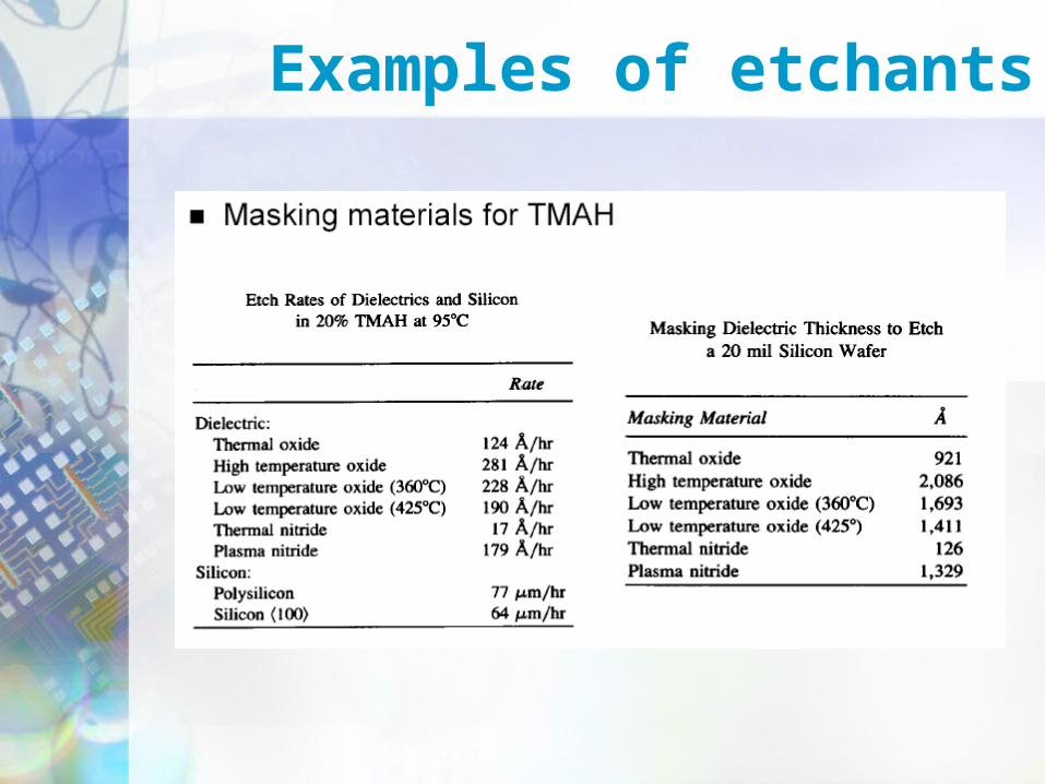
Examples of etchants

Etch Stop

Deep reactive ion etching

Dry anisotropic etching

Deep reactive ion etching

Dry isotropic etching

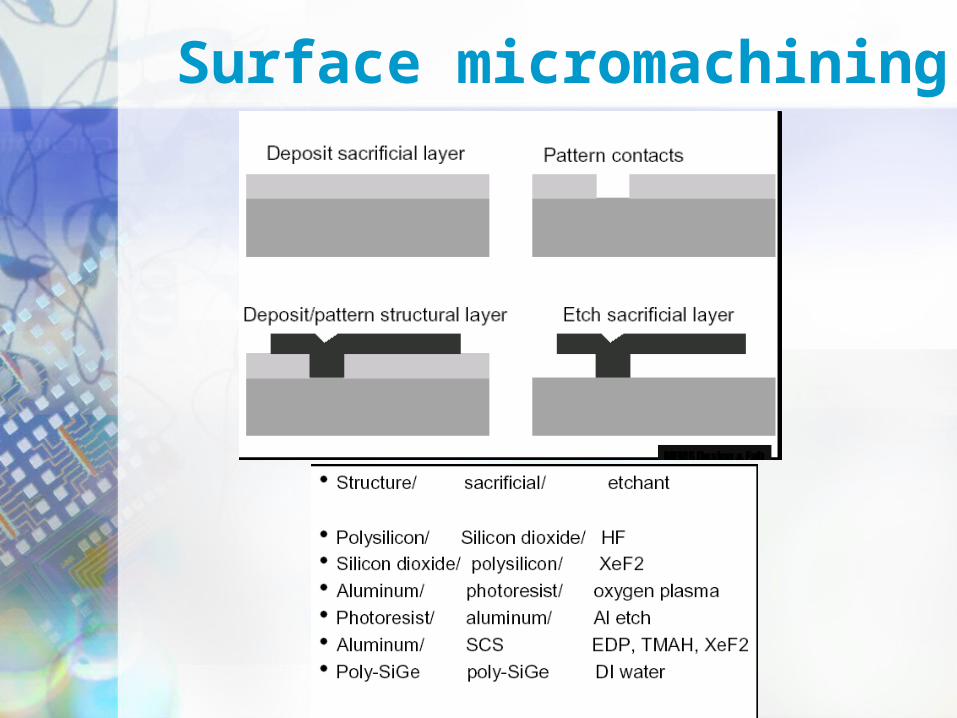
Surface micromachining • In the case of surface micromachining,a different
approach is taken in that rather than etching into the bulk of the starting material, structures are built up on the substrate surface
• These structures are created via the repetitive addition of layers selected for their various material properties, followed by the selective removal of these layers in a specific sequence.
• The vast array of materials that can be “deposited” includes polysilicon, silicon nitride, oxide, polyimide, metals, etc.
Surface micromachining

Surface micromachining
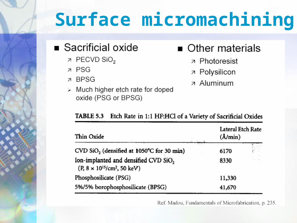
Surface micromachining

Sticktion!
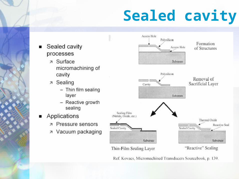
Sealed cavity

Examples
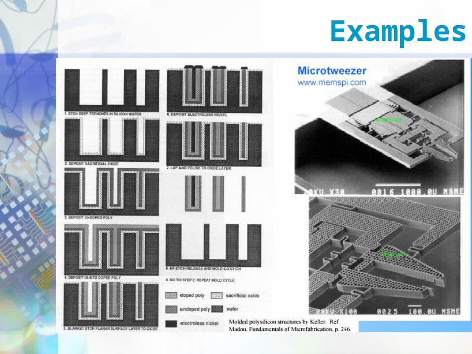
Examples

Bulk vs Surface
• Both bulk and surface micromachining concepts are most often combined to create both intricate and simple devices and systems.
• Other observations (M.J. Madou):

LIGA
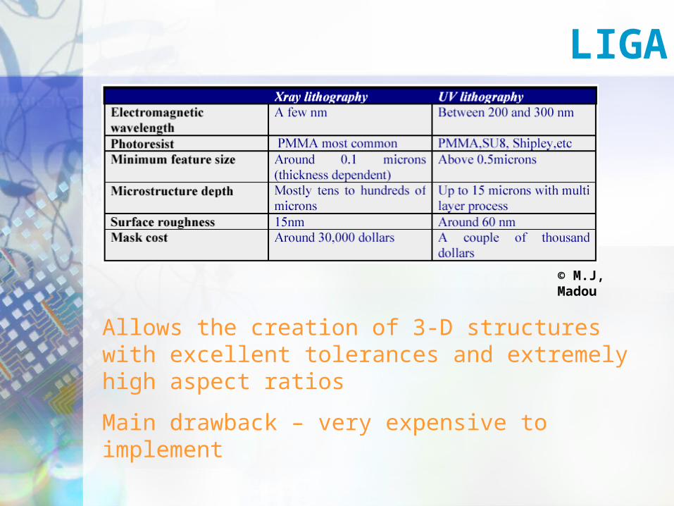
© M.J, Madou
LIGA
Allows the creation of 3-D structures with excellent tolerances and extremely high aspect ratios
Main drawback – very expensive to implement
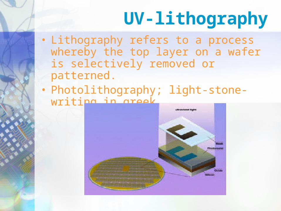
UV-lithography • Lithography refers to a process whereby the
top layer on a wafer is selectively removed or patterned.
• Photolithography; light-stone-writing in greek

UV-lithography

Laser Sources
Wmin = k1 .
NA
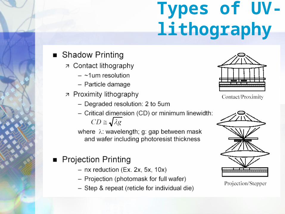
Types of UV-lithography

UV-lithography • Mask making
• Resist spinning
• Alignment of wafer and mask
• Resist tone, Tg, critical dimensions
• Lithography resolution
• Depth of Focus
• Resist wall profile manipulation
• Clean-rooms, wafer cleaning
• Process sequence
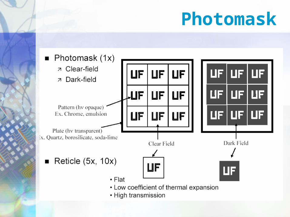
Photomask
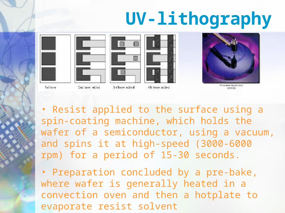
UV-lithography
• Resist applied to the surface using a spin-coating machine, which holds the wafer of a semiconductor, using a vacuum, and spins it at high-speed (3000-6000 rpm) for a period of 15-30 seconds.
• Preparation concluded by a pre-bake, where wafer is generally heated in a convection oven and then a hotplate to evaporate resist solvent
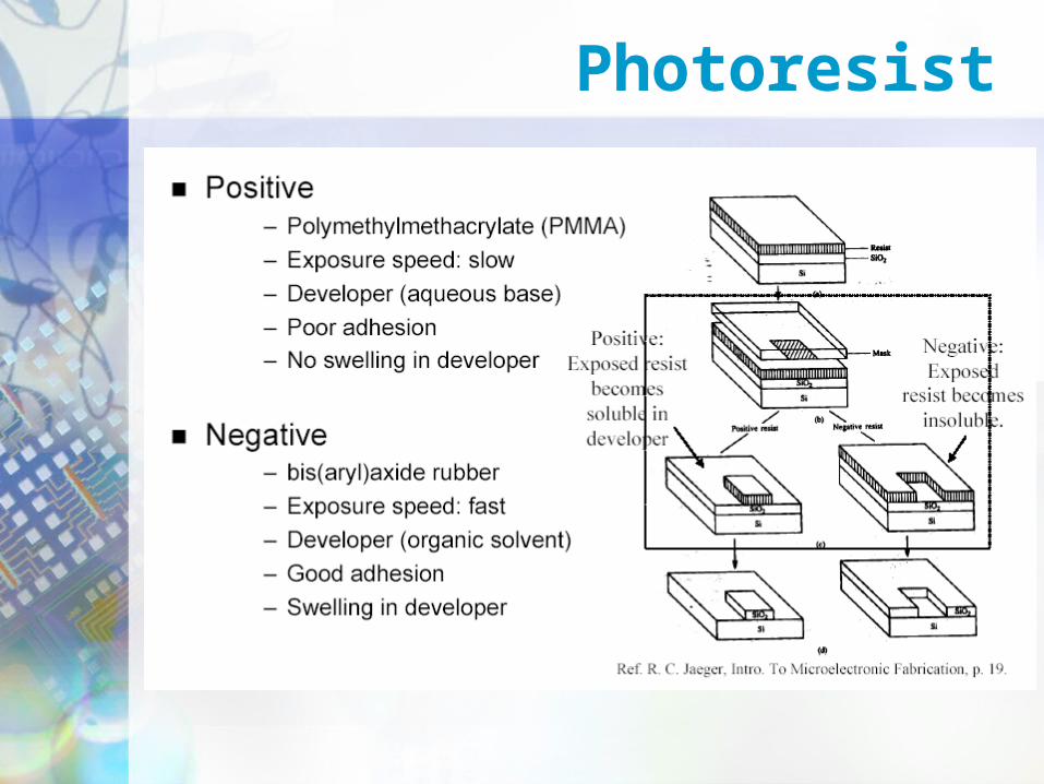
Photoresist

Developer

Process

UV-lithography

UV-lithography
• Fiducals are patterns used for alignment on wafer steppers. These fiducials are located outside of the array or fields.
• Alignment of the mask is critical and must be achieved in the x-y plane
• Double alignment is especially important in the fabrication of micromachines

UV-lithography Negative and positive resist
Tg - glass transition temperature - important not to work above the Tg as is very easy to pick up dirt
CD - critical dimension - is the minimum width that is allowed as part of the circuit design (e.g. The CD in a pentium V chip is 0.18m)

Example
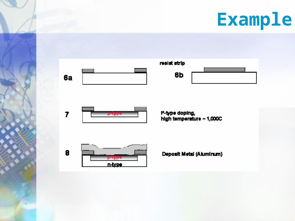
Example
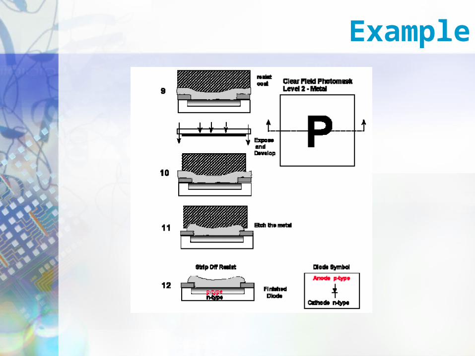
Example

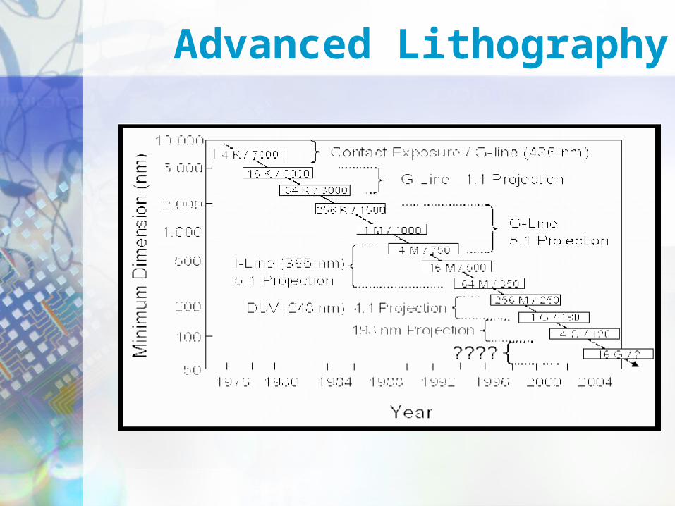
Advanced Lithography
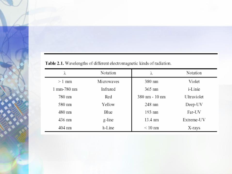
Wavelengths started with the g-line (436 nm) of Hg - good down to 0.4m
Next came the 365nm i-line in the near-UV - this took us down to 0.3m
BUT no light bulb that emits enough intensity at wavelengths considerably smaller than 365nm
The solution was excimer lasers - 248nm, 194nm and 157nm (deep UV lithography)
this spelt …… the END of UV-lithography!
Advanced Lithography

Advanced Lithography
• Electron-beam lithography
• Ion beam lithography
• X-ray lithography
• Extreme UV-lithography
Wmin = k1 .
NA Reduce k1
Reduce
Increase NA

Advanced Lithography

Extreme UV Lithography
Technology breakthrough - 13.4nm wavelength of this light is more than 10 times shorter - allows patterning of lines below 50nm dimensions
Intel leading a consortium of six semiconductor companies called the EUV LLC to develop this technology

Electron beam Lithography
Pattern directly written into resist by scanning e-beam
Eliminates the diffraction limits of optical lithography
Performance records:
- in PMMA (organic resist): 7nm
- in AlF3(inorganic resist): 2nm

Optical Electron Beam
Advantage
Low ~High precision Fast exposure speed Relatively low cost
No diffraction Easy to control Available for small features
Disadvantage
Light diffraction Alignment problem Debris between mask and wafer
Needs vacuum High system cost Slow
UV vs E-beam Lithography

Ion-beam Lithography• Variation of the electron-beam lithography technique - uses a focused ion beam instead of an electron beam
• The ions are field extracted from a liquid metal ion source (LMIS) that consists of a tungsten needle with a radius of curvature of 1mm that is wetted by a liquid metal.
• The application of an electric field (>108cm/V) to the wetted tip results in the formation of a cone with a radius of curvature of 10nm from which the ions are field extracted
• The extracted ions are accelerated, collimated and focused by a series of apertures and electrostatic lenses
• Spot-sizes of 10nm to 500nm are possible.

Ion-beam Lithography

X-ray Lithography
As shown in this figure, the penumbral blur, , on the adge of the resist image is given by:
= ag/L
a is the diameter of the x-ray source
g is the gap between mask and wafer
L is the distance from the source to the x-ray mask

Soft LithographyTransfer of a self-assembled monolayer precursor with an elastomeric stamp onto a substrate
1) A master is generated by photolithography and a stamp is obtained by casting of an elastomer (PDMS etc.)
2) A pattern is generated by stamping a SAM on a substrate

Deposition
a) Chemical Vapor Deposition (CVD) systemsWhich rely on the chemical reaction of the constituents of a vapor phase at the substrate surface to deposit a solid film on this surface.
b) Physical Vapor Deposition (PVD) systemsWhich directly deposit the source material onto a given substrate in a “line-of-site impingement type deposition”.
Deposition systems may be divided into two groups:

a) CVD: Summary of transport and reaction
processes
© L.M. Landsberger
Deposition
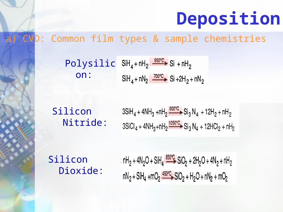
a) CVD: Common film types & sample chemistries
Polysilicon:
Silicon Nitride:
Silicon Dioxide:
Deposition

a) CVD: Atmospheric Systems (APCVD)
Cold-wall induction type with tilted susceptor
Barrel type
Rotating pancake type
Poly Si deposition: Note the use of a liquid source in this example (SiCl4)
Induction heating: RF energy couples with the graphite susceptor, thereby heating it rather than
heating the process gases and substrates themselves (improved contamination control)
Deposition
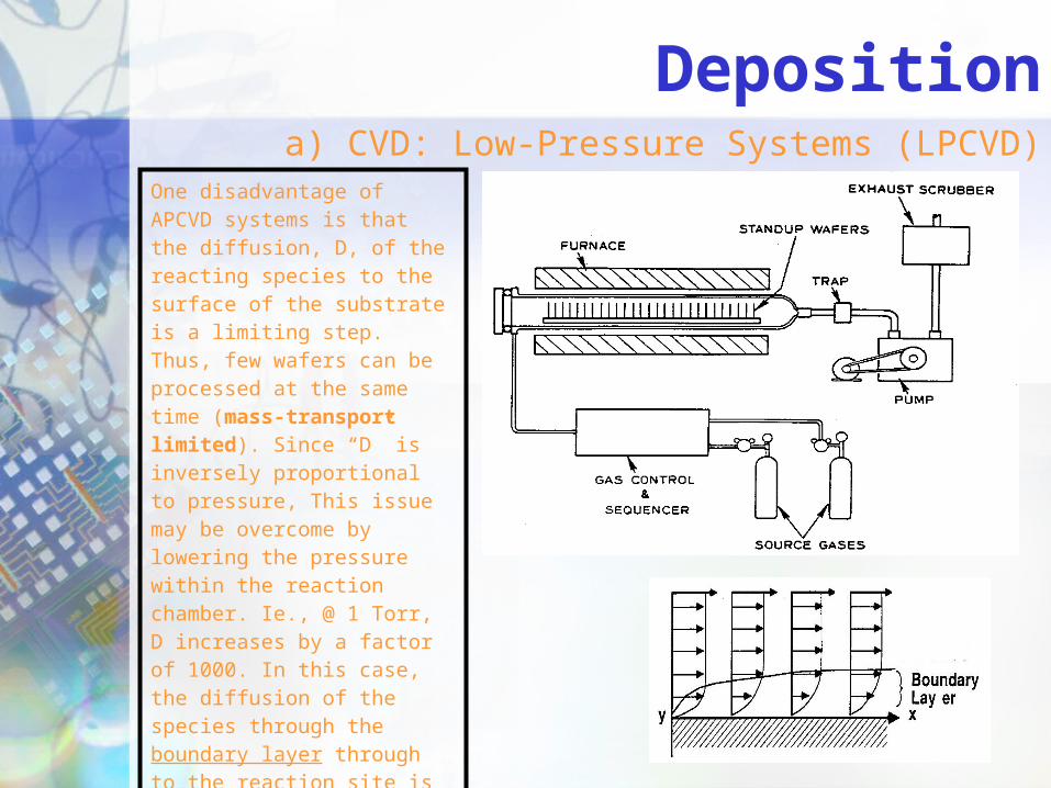
a) CVD: Low-Pressure Systems (LPCVD)One disadvantage of APCVD systems is that the diffusion, D, of the reacting species to the surface of the substrate is a limiting step. Thus, few wafers can be processed at the same time (mass-transport limited). Since “D” is inversely proportional to pressure, This issue may be overcome by lowering the pressure within the reaction chamber. Ie., @ 1 Torr, D increases by a factor of 1000. In this case, the diffusion of the species through the boundary layer through to the reaction site is no longer a limiting step and the system is said to be surface reaction limited.
Deposition
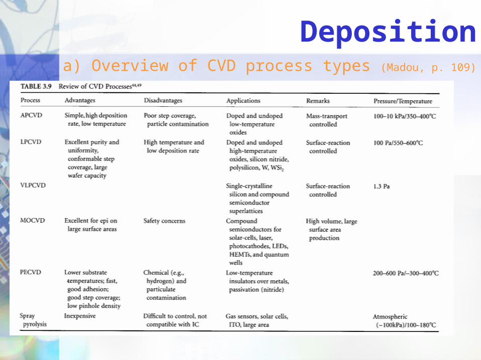
a) Overview of CVD process types (Madou, p. 109)
Deposition

b) Physical Vapor Deposition (PVD) systems
– In these types of thin film deposition systems, the source materials to be deposited take on a variety of forms:
• Solid• Liquid• Vapor
– In the case of PVD systems, the materials to be deposited are physically deposited using a variety of methods including:
• Thermal Evaporation • Sputtering• Etc. (Laser Ablation, Molecular Beam Epitaxy)
Deposition

a) Physical Vapor Deposition (PVD) systems -
continued
– The range of materials that may be deposited using these methods include:
• Metals such as:
– Al – Cu– Au– Ag– etc.
• Compound & hard materials such as:
– Cr– TiN– CrN– AlCuSi– etc.
Deposition
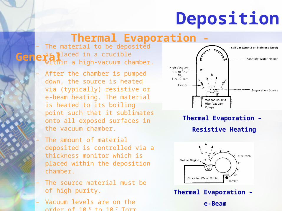
– The material to be deposited is placed in a crucible within a high-vacuum chamber.
– After the chamber is pumped down, the source is heated via (typically) resistive or e-beam heating. The material is heated to its boiling point such that it sublimates onto all exposed surfaces in the vacuum chamber.
– The amount of material deposited is controlled via a thickness monitor which is placed within the deposition chamber.
– The source material must be of high purity.
– Vacuum levels are on the order of 10-5 to 10-7 Torr.
Thermal Evaporation –
Resistive Heating
Thermal Evaporation –
e-Beam
Thermal Evaporation - General
Deposition

Thermal Evaporation - drawbacks
– Resistive heating is the simplest method of evaporating metals such as Al
or Au, but it is also the “dirtiest” in that contaminants which find their way
onto the filament tend to be evaporated along with the metal.
– The purity issue can be addressed via e-beam evaporation since the
cooled, non-molten high-purity material to be deposited acts as a crucible
during the process (see schematic on previous slide).
– In the case of resistive heating, temperature uniformity across the filament
is difficult to control and therefore, evaporation uniformity onto the
substrates may be a problem. This is not an issue with e-beam
evaporation
– E-beam evaporation may cause surface damage due to ionizing radiation
and/or X-rays (@ voltages above 10kV, the incident electron beam will
give rise to X-ray emission).
Deposition
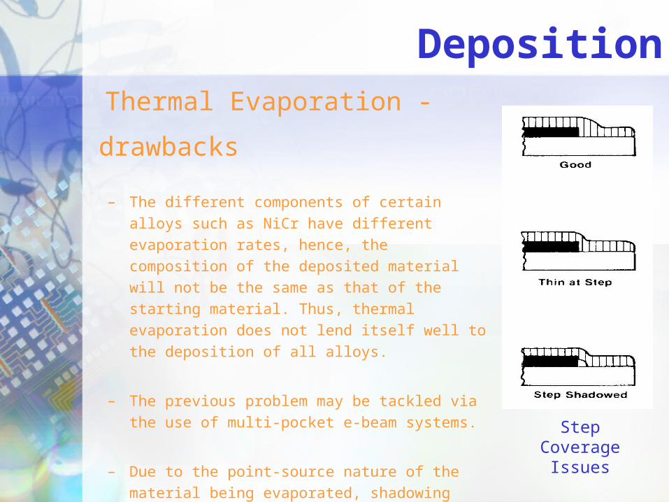
Thermal Evaporation - drawbacks
– The different components of certain alloys such as
NiCr have different evaporation rates, hence, the
composition of the deposited material will not be the
same as that of the starting material. Thus, thermal
evaporation does not lend itself well to the deposition
of all alloys.
– The previous problem may be tackled via the use of
multi-pocket e-beam systems.
– Due to the point-source nature of the material being
evaporated, shadowing effects may hamper the
uniformity of the deposited layer over steps existing on
the substrate (bad step coverage) in both the e-beam
& resistive heating cases.
Step Coverage Issues
Deposition

Sputtering
Sputtering – principle of operation• A solid slab (ie., target) of the material to be deposited is placed in a
vacuum chamber along with the substrate on which the deposition is to
take place.
• The target is grounded.
• Argon gas is introduced into the chamber and ionized to a positive
charge.
• The Ar ions bombard the target and cause the target atoms to scatter,
with some of them landing on the substrate.
• The plasma is composed of the Ar atoms, Ar ions, the sputtered
material, gas atoms and electrons generated by the sputtering process.
• Allows the deposition of a large assortment of materials on any type of
substrate
Deposition

Deposition: sputtering

Sputtering – advantages/disadvantages
M.J. Madou
Deposition

Ink-jet micromachining

Process Flow
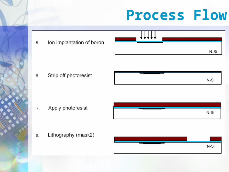
Process Flow

Process Flow
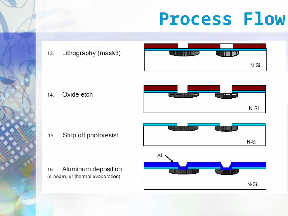
Process Flow

Process Flow

a) Find a research article detailing AFM or
STM being applied to a biological
application from 2003-2004 and make a
summary of this article (Hint: Check current
contents)
b) Think of 5 potential applications of
nanoparticles
Homework
Recommended