Copyright 2007, Toshiba Corporation.
April 2013 Semiconductor & Storage Products Company Toshiba Corporation
Toshiba Group contributes to
the sustainable future of planet Earth. © 2013 Toshiba Corporation
Power Management Wireless Power LSI
MAY 2013
“TB6865FG” WPC Transmitter
“TB6860WBG” WPC Receiver and Charger
“TB6862WBG“ WPC High Efficiency Receiver
“TC7761WBG“ WPC High Efficiency Single Chip Receiver

2
System Block Diagram of TOSHIBA LSI
Messages
Power
MCU
Modulation
Ba
tte
ry
Rectifier
(Power Pickup)
DCDC
Charger
Control
TB686x series
Receiver
■TB6865FG Feature
Cost and space saving by 1Package (MCU + Analog)
2-device (Rx) Charging simultaneously
(Control is possible by 2 devices)
Positioning free (2 Coil control architecture)
Transmitter
AC Adapter
ID x n Detector
Coil_sel_sw1 x n TB6865FG
~
Filter P
re D
rive
r
PW
M
Full Bridge
Switch Control
Coil Unit
A
Coil Unit
B
MCU
■TB6860WBG Feature
Quick charge by DCDC SW Converter.
(High Current Output 1.2A)
Programmable Charging Profile
(I2C control) Protection Circuits/Detection (Input Voltage, Output current, thermal)
WPC A12
or A14 type

3 Toshiba Confidential
1. Wireless Power IC
Product Lineup

4
TB6860WBG WPC Receiver and Charger LSI
TB6862WBG WPC High Efficiency Receiver
TC7761WBG High Efficiency Receiver
System
block
Mode Charging mode (CC) / Voltage feed (CV) Voltage feed (CV) Voltage feed (CV)
Merit
• Designs system without charger IC
• Maximum output current : 1.2A
• Can use your original Software
• Strong against IC heat at 5W
• Efficiency 92% @ 5W output
• Maximum output current : 1.2A
• Can use your original Software
• Designs system without MCU.
• FOD (WPC Ver. 1.1)
• High Efficiency by Toshiba process
Protection
• Over voltage/ Under voltage lockout
• Over current limit
• Thermal shutdown
• Over voltage/ Under voltage lockout
• Over current limit
• Thermal shutdown
• Over voltage/ Under voltage lockout
• Over voltage clamper
• Over current limit
• Thermal shutdown
Application Battery pack / Smart phone / Mobile Accessory Smart Phone / Mobile Accessory Smart Phone / Mobile Accessory
Package WCSP 39 (4.25mm x 2.65mm) WCSP 39 (4.25mm x 2.65mm) WCSP 28 (2.4mm x 3.67mm *tentative)
Toshiba Wireless Power Receiver Line up
Toshiba Confidential
Charger
Battery
MCU MCU
Rectifier
DC-DC charger
Rectifier
DC-DC conv.
Rectifier
LDO
Modulator Modulator
Modulator
Charger
Battery
Battery
Coil
Input switch
Controller Coil
Coil
5
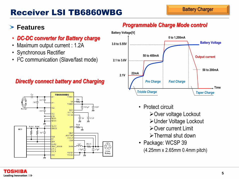
Receiver LSI TB6860WBG
• DC-DC converter for Battery charge
• Maximum output current : 1.2A
• Synchronous Rectifier
• I2C communication (Slave/fast mode)
Battery Charger
Features
Time
2.1V
Battery Voltage[V]
22mA
50 to 400mA
2.1 to 3.6V
0 to 1,200mA
3.0 to 5.55V
50 to 200mA
Trickle Charge
Pre Charge Fast Charge
Taper Charge
Output current
Battery Voltage
Programmable Charge Mode control
Directly connect battery and Charging
• Protect circuit
Over voltage Lockout
Under Voltage Lockout
Over current Limit
Thermal shut down
• Package: WCSP 39
(4.25mm x 2.65mm 0.4mm pitch)

6
Receiver LSI TB6862WBG
• Synchronous Rectifier
• I2C communication (Slave/fast mode)
• Maximum output current : 1.2A
High efficiency
Features
Voltage feed mode
Efficiency 92% @ 5W output
Tx: A14 type product made by Hanrim
Rx: TSB EVB(Vout 5[V])
TB6862WBG:92% (5W output)
TB6860WBG:87% (5W output)
RX Module Efficiency
Output [W]
Eff
icie
nc
y [
%]
• Protect circuit
Over / Under voltage lockout
Over current Limit
Thermal shut down
• Package: WCSP 39 (4.25mm x 2.65mm 0.4mm pitch)

7
TB6862WBG Advantage (efficiency at 5W)
Receiver Efficiency
Measurement condition Tx : TI EVB (bq500211 TX EVB)
RX: TSB EVB type 1
* From AC input to DC output
70.00%
75.00%
80.00%
85.00%
90.00%
95.00%
100.00%
1 2 3 4 5
Eff
icie
nc
y
(%)
Out put Power [W]
TB6862WBG
TB6862WBG Competitor LSI
TB6862WBG Efficiency is keep over 90% at heavy load ( 92% @ 5W)
8
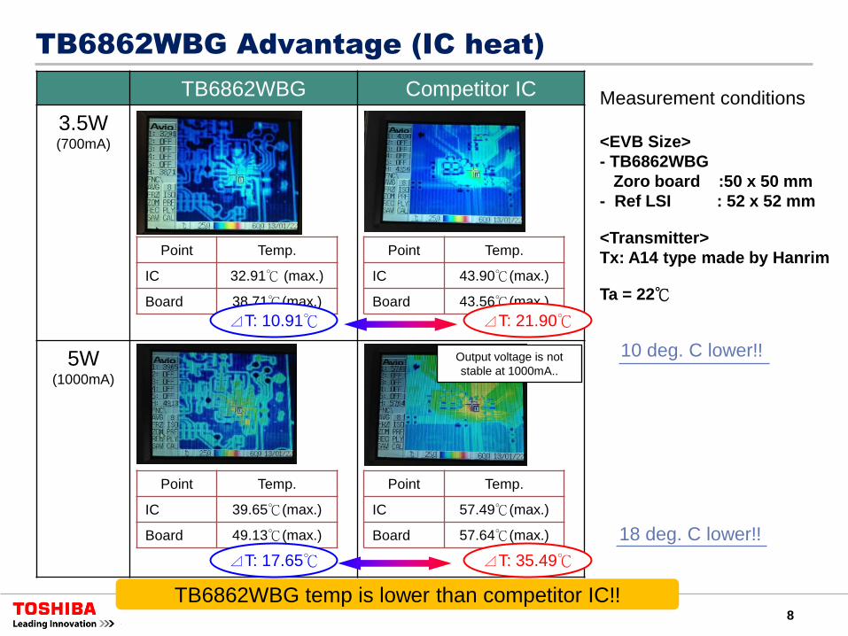
TB6862WBG Advantage (IC heat)
TB6862WBG Competitor IC
3.5W (700mA)
5W (1000mA)
Point Temp.
IC 32.91℃ (max.)
Board 38.71℃(max.)
Point Temp.
IC 43.90℃(max.)
Board 43.56℃(max.)
Point Temp.
IC 39.65℃(max.)
Board 49.13℃(max.)
Point Temp.
IC 57.49℃(max.)
Board 57.64℃(max.)
⊿T: 10.91℃ ⊿T: 21.90℃
⊿T: 17.65℃ ⊿T: 35.49℃
TB6862WBG temp is lower than competitor IC!!
Measurement conditions
<EVB Size>
- TB6862WBG
Zoro board :50 x 50 mm
- Ref LSI : 52 x 52 mm
<Transmitter>
Tx: A14 type made by Hanrim
Ta = 22℃
10 deg. C lower!!
18 deg. C lower!!
Output voltage is not
stable at 1000mA..

9 Toshiba Confidential
2. TC7761WBG
Technology

10
TC7761WBG Concept
Toshiba Confidential
Shrink System size, Reduce System cost
High Efficiency / Reduce thermal problem !!
The Charger time is same with wired Charger
Foreign object Detection for WPC Ver 1.1
Satisfy latest WPC spec
Reduce Ron
1 chip solution
WPC Ver 1.1

11
Receiver LSI TC7761WBG
1 chip Solution
• WPC Ver. 1.1 compliant
• Synchronous Rectifier
• 5V / 1A Output LDO
include Load Switch Mode
• External Load Switch Driver
• Protect Circuits
Under Voltage Lockout (PVDD / SW_DET)
Over Voltage Lockout (SW_DET)
Over Voltage Clamper (PVDD)
Over current Limiter (5V LDO)
Thermal Shutdown
• WCSP 28
(0.5mm pitch)
Features

12
TC7761WBG Ron Approach
Toshiba Confidential
1. W/W No1 DMOS Ron A resistance
Toshiba 0.13um Process applying for TC7761WBG.
2. Process tuning for TC7761WBG
New layout structure, improve internal process R
3. Simulation for suitable DMOS size
to check good valance DMOS cell number

13
0
10
20
30
40
50
60
70
80
2000 2005 2010 2015
RonA[m
Ω・mm2
]@Ra
ted Vo
ltage=
40V
TISTTSB
CD-0.13 2nd.Gen.
BiCD-0.35
BiCD-0.13 1st.Gen.
BiCD-0.6i
0.6um
A: 0.18um Gen. 2011 release (Plan)
B: 0.13um Gen. 2012 release (Plan)
0.35um
0.18um
0.5um
0.35um 0.25um
◆ Company-A
■ Company-B
● TOSHIBA
Developed the low
Ron-process ahead of
the competitor
Toshiba developed the
suitable process for the
switching regulator IC
DMOS Area shrink
Reduction of Ciss=
High efficiency
Realize chip shrink and high efficiency by Toshiba advanced 0.13μm analog process
★ World wide No.1Ron A resistance
0
20
40
60
80
100
120
140
160
180
200
20 30 40 50 60 70
Pch LDMOS Rated Voltage[V]
Ron
A [
mΩ・ m
m2]
STM BCD6(0.35um)
STM BCD8(0.18um)
Toshiba BiCD-0.13(0.13um)
Pch LDMOS
Pch LDMOS Rated Voltage[V]
RonA
[m
ohm・m
m2]
0
20
40
60
80
100
120
140
160
180
200
20 30 40 50 60 70
Nch LDMOS Rated Voltage[V]
Ron
A [m
Ω・ m
m2]
TI LBC5(0.35um)
TI LBC7(0.25um)
STM BCD6(0.35um)
STM BCD8(0.18um)
Toshiba BiCD-0.6(0.6um)
Toshiba BiCD0-0.35(0.35um)
Toshiba BiCD-0.13(0.13um)
Company-A (0.35um)
Company-A (0.25um)
Company-B (0.35um)
Company-B (0.18um)
TOSHIBA (0.6um)
TOSHIBA (0.35um)
TOSHIBA (0.13um)
Company-B (0.35um)
Company-B (0.18um)
TOSHIBA (0.13um)
RonA
[m
ohm・m
m2]
Nch LDMOS Rated Voltage[V]
TOSHIBA 0.13um TOSHIBA 0.13um
Nch LDMOS
Rate
d V
olta
ge
[V
]
TOSHIBA 0.13um DMOS process
TC7761WBG realize high efficiency by using this technology!!
14
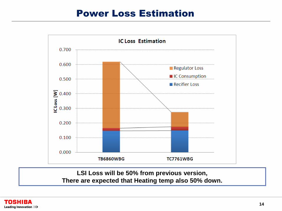
Power Loss Estimation
LSI Loss will be 50% from previous version,
There are expected that Heating temp also 50% down.
15 2013/6/19
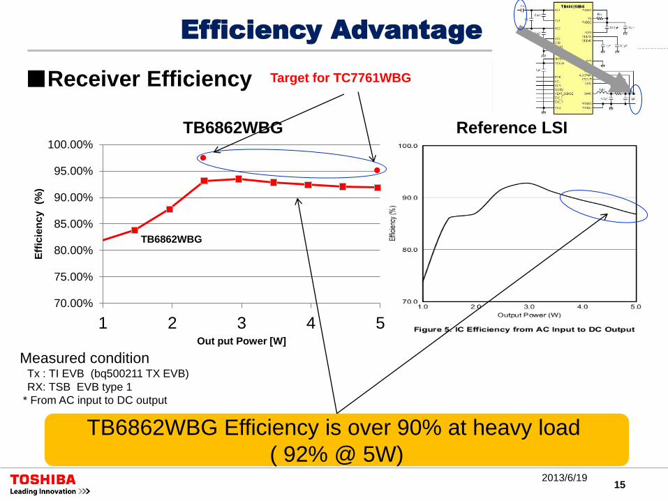
Efficiency Advantage
■Receiver Efficiency
Measured condition Tx : TI EVB (bq500211 TX EVB)
RX: TSB EVB type 1
* From AC input to DC output
70.00%
75.00%
80.00%
85.00%
90.00%
95.00%
100.00%
1 2 3 4 5
Eff
icie
nc
y
(%)
Out put Power [W]
TB6862WBG
TB6862WBG Reference LSI
TB6862WBG Efficiency is over 90% at heavy load
( 92% @ 5W)
• •
Target for TC7761WBG
16
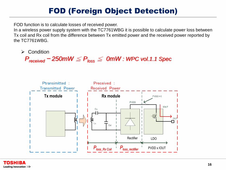
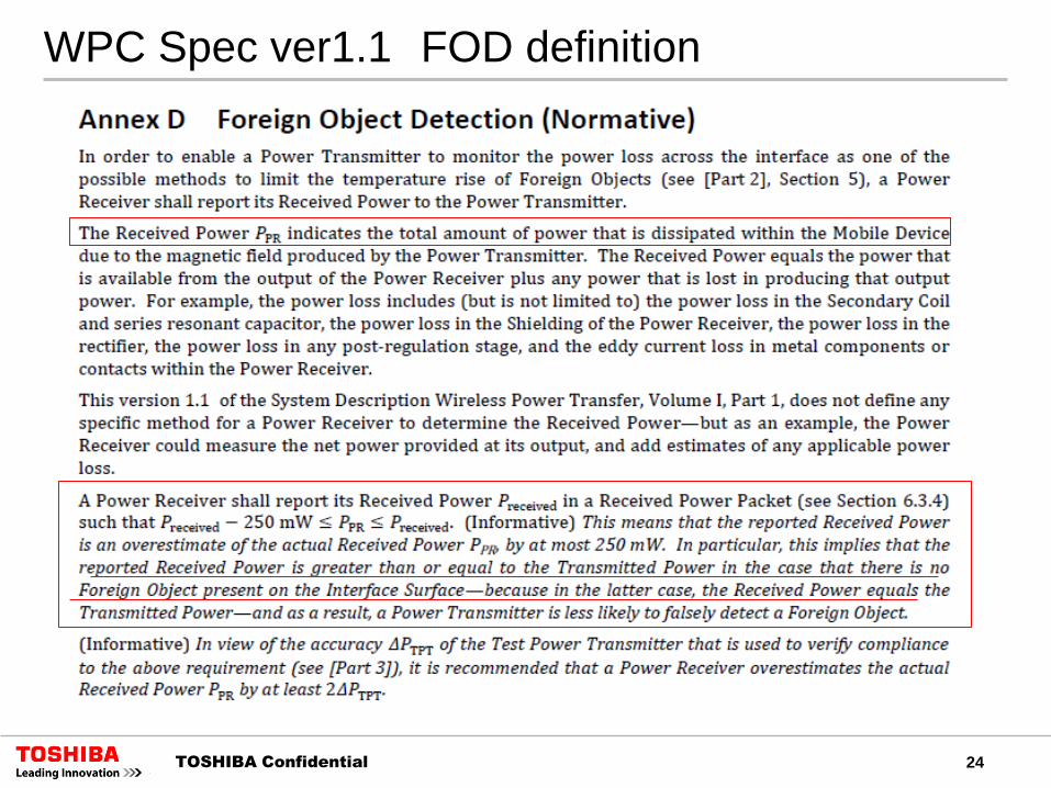
FOD (Foreign Object Detection)
Condition
Preceived ー 250mW ≦ Ploss ≦ 0mW : WPC vol.1.1 Spec
FOD function is to calculate losses of received power.
In a wireless power supply system with the TC7761WBG it is possible to calculate power loss between
Tx coil and Rx coil from the difference between Tx emitted power and the received power reported by
the TC7761WBG.
Rx module Tx module
Ploss_rectifier Ploss_Rx Coil
Rectifier LDO
PVDD x IOUT

17
•Suitable for A12 and A14 transmitter type (free positioning)
•The Charging area of Type A14 type is 27 mm x 68 mm
•Can drive 2 transmitters (provide power to 2 receivers simultaneously)
•Cortex-M3 Core
•High Resolution PWM 8CH(100Hz step)
•Built-in LDO
• Built-in Pre Driver (Drive 4xFull Bridge circuit)
• 12bit ADC 14CH
• Protector
Over voltage
Over current
Thermal shut down
•LQFP 100 14x14mm 0.5mm pitch
Power Controller
AC
Adapter
Buzzer
LED
Temp
Sensor
ID x n Detector
Coil_sel_sw1 x n
TB6865WBG
~
Cortex-M3
Filter
Pre
Drive
r
PW
M
Full
Bridge
Switch Control
Digital Part
Analog Part
Transmitter LSI TB6865FG
Two Devices system
example
Features

18
TX type A14 A12 A1/A5/A10/A11 A6 A2 A3
IC Vendor TOSHIBA Company A General purpose IC ASIC
Method
Free Position Guided position
Magnetic or
No Magnetic
Free
Position
Free Position
(Moving Coil)
Free position
(Multi Coil )
Number of Coil 2 Coil 1 Coil 1 Coil 3 Coil 1 Coil+Motor
+XY Senser
7 Coil
(PCB/Coil)
MAX. Number of
Charging Device 2 Device 1 Device 1 Device 1 Device 1 Device
WPC
Type
Device
Position
Number
of Coil
Maximum
Number of
Charging
Device
Receiver Charger(Rx)
Method Fast Charge current in
Charger mode(A)
TOSHIBA Free 2 or 1 2 DC/DC (CC-CV) 1.2A
A1/5/6/10/11 Center/Free 3 or 1 1 LDO (CV) 0.7A
A3 Free 7 (Cost up) 1 LDO(CV) 1A
Tx (1) Free positioning system based on only 1 or 2coil architecture. Tx (2) No effect for the receiving & GPS sensitivity without magnetic material. Tx (3) Realize maximum 2 devices charger solution. Rx (4) High efficiency and High charging current by internal DC/DC converter
TOSHIBA Wireless Power System Merit
Easy Charging !

19
Rx EVB (ZORO Board)
• Evaluation board for TB6860WBG (CV mode)
and TB6862WBG
• MCU : MCU (TMPM341FDXBG)
• EVB size : 50mm x 50mm
Evaluation Board
Tx EVB A12 (NAMI Board)
• Evaluation board for TB6865FG
• EVB size : 128mm x 74mm
Tx EVB A14 (NICO Board)
• Evaluation board for TB6865FG
• EVB size : 163mm x 74mm
TB6860/62WBG
TB6865FG
TB6865FG
A12 Coil
A14 Coil
TMPM341FDXBG
TRx-483265-15F5-G (TDK)

20
New Rx EVB (TC7761WBG )
•Evaluation board for TC7761WBG
•EVB size : 50mm x 50mm
New Evaluation Board
TC7761WBG
21
2012 2013 2014
TB6860WBG
Rectifier
Modulator
TC7761WBG
Mid Power
for quick charging
DCDC
Charger
Input switch
Controller
LDO
TBXXX
DCDC
Charger
(8W to 15W)
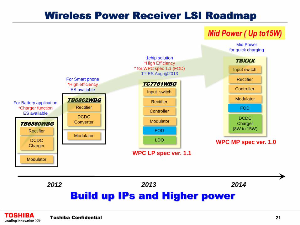
Rectifier
Wireless Power Receiver LSI Roadmap
Build up IPs and Higher power
1chip solution
*High Efficiency
* for WPC spec 1.1 (FOD)
1st ES Aug @2013
WPC MP spec ver. 1.0
For Battery application
*Charger function
ES available
TB6862WBG
Rectifier
Modulator
DCDC
Converter
For Smart phone
*High efficiency
ES available
FOD
WPC LP spec ver. 1.1
Modulator
Input switch
Controller
Rectifier
FOD
Modulator
Toshiba Confidential
Mid Power ( Up to15W)
22
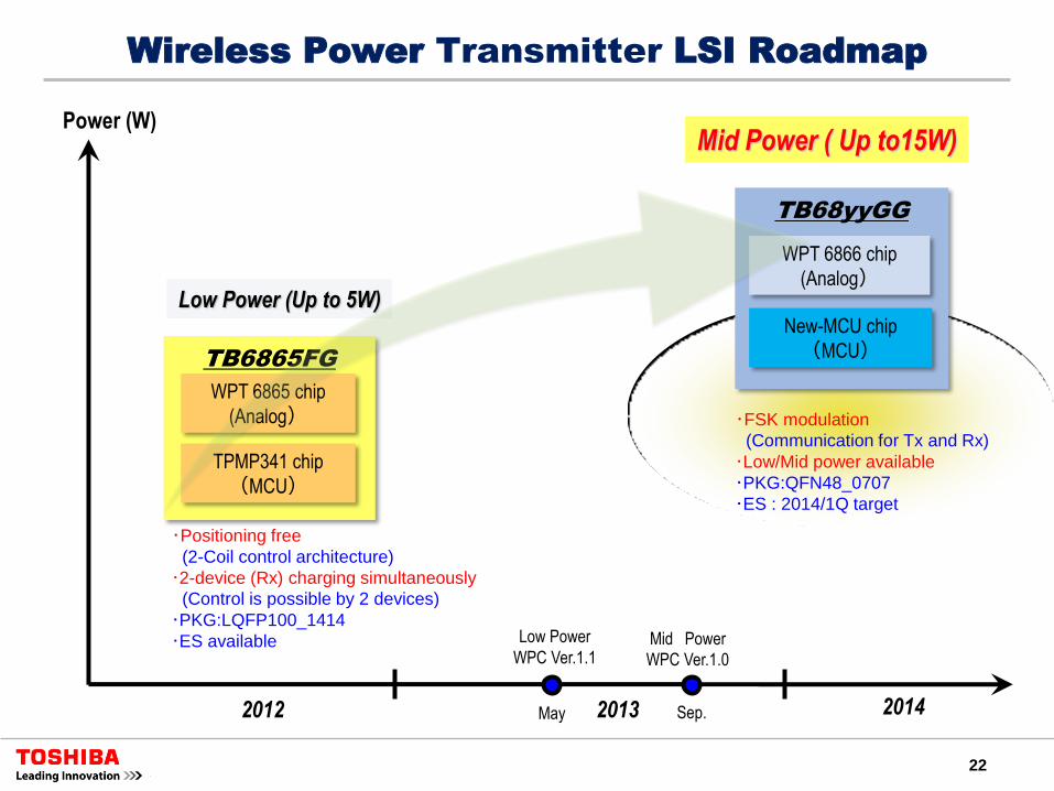
Power (W)
Low Power (Up to 5W)
Mid Power ( Up to15W)
TB6865FG
WPT 6865 chip
(Analog)
TPMP341 chip
(MCU)
TB68yyGG
New-MCU chip
(MCU)
WPT 6866 chip
(Analog)
2012 2013
Low Power
WPC Ver.1.1 Mid Power
WPC Ver.1.0
May Sep.
Wireless Power Transmitter LSI Roadmap
・Positioning free
(2-Coil control architecture)
・2-device (Rx) charging simultaneously
(Control is possible by 2 devices)
・PKG:LQFP100_1414
・ES available
・FSK modulation
(Communication for Tx and Rx)
・Low/Mid power available
・PKG:QFN48_0707
・ES : 2014/1Q target
2014
23 TOSHIBA Confidential
FOD
24
WPC Spec ver1.1 FOD definition
TOSHIBA Confidential

25
WPC Reference tester
Qi Tester
– Every WPC member have to pass this spec by WPC reference tester in test house
– Toshiba have plan to invest this equipment this year.
TOSHIBA Confidential
26
RESTRICTIONS ON PRODUCT USE Toshiba Corporation, and its subsidiaries and affiliates (collectively “TOSHIBA”), reserve the right to make changes to the information in this document, and related hardware, software
and systems (collectively “Product”) without notice.
This document and any information herein may not be reproduced without prior written permission from TOSHIBA. Even with TOSHIBA’s written permission, reproduction is
permissible only if reproduction is without alteration/omission.
Though TOSHIBA works continually to improve Product’s quality and reliability, Product can malfunction or fail. Customers are responsible for complying with safety standards and for
providing adequate designs and safeguards for their hardware, software and systems which minimize risk and avoid situations in which a malfunction or failure of Product could cause
loss of human life, bodily injury or damage to property, including data loss or corruption. Before creating and producing designs and using, customers must also refer to and comply
with (a) the latest versions of all relevant TOSHIBA information, including without limitation, this document, the specifications, the data sheets and application notes for Product and the
precautions and conditions set forth in the “TOSHIBA Semiconductor Reliability Handbook” and (b) the instructions for the application that Product will be used with or for. Customers
are solely responsible for all aspects of their own product design or applications, including but not limited to (a) determining the appropriateness of the use of this Product in such
design or applications; (b) evaluating and determining the applicability of any information contained in this document, or in charts, diagrams, programs, algorithms, sample application
circuits, or any other referenced documents; and (c) validating all operating parameters for such designs and applications. TOSHIBA ASSUMES NO LIABILITY FOR CUSTOMERS’
PRODUCT DESIGN OR APPLICATIONS.
Product is intended for use in general electronics applications (e.g., computers, personal equipment, office equipment, measuring equipment, industrial robots and home electronics
appliances) or for specific applications as expressly stated in this document. Product is neither intended nor warranted for use in equipment or systems that require extraordinarily high
levels of quality and/or reliability and/or a malfunction or failure of which may cause loss of human life, bodily injury, serious property damage or serious public impact (“Unintended
Use”). Unintended Use includes, without limitation, equipment used in nuclear facilities, equipment used in the aerospace industry, medical equipment, equipment used for automobiles,
trains, ships and other transportation, traffic signaling equipment, equipment used to control combustions or explosions, safety devices, elevators and escalators, devices related to
electric power, and equipment used in finance-related fields. Do not use Product for Unintended Use unless specifically permitted in this document.
Do not disassemble, analyze, reverse-engineer, alter, modify, translate or copy Product, whether in whole or in part.
Product shall not be used for or incorporated into any products or systems whose manufacture, use, or sale is prohibited under any applicable laws or regulations.
The information contained herein is presented only as guidance for Product use. No responsibility is assumed by TOSHIBA for any infringement of patents or any other intellectual
property rights of third parties that may result from the use of Product. No license to any intellectual property right is granted by this document, whether express or implied, by estoppel
or otherwise.
ABSENT A WRITTEN SIGNED AGREEMENT, EXCEPT AS PROVIDED IN THE RELEVANT TERMS AND CONDITIONS OF SALE FOR PRODUCT, AND TO THE MAXIMUM
EXTENT ALLOWABLE BY LAW, TOSHIBA (1) ASSUMES NO LIABILITY WHATSOEVER, INCLUDING WITHOUT LIMITATION, INDIRECT, CONSEQUENTIAL, SPECIAL, OR
INCIDENTAL DAMAGES OR LOSS, INCLUDING WITHOUT LIMITATION, LOSS OF PROFITS, LOSS OF OPPORTUNITIES, BUSINESS INTERRUPTION AND LOSS OF DATA,
AND (2) DISCLAIMS ANY AND ALL EXPRESS OR IMPLIED WARRANTIES AND CONDITIONS RELATED TO SALE, USE OF PRODUCT, OR INFORMATION, INCLUDING
WARRANTIES OR CONDITIONS OF MERCHANTABILITY, FITNESS FOR A PARTICULAR PURPOSE, ACCURACY OF INFORMATION, OR NONINFRINGEMENT.
Do not use or otherwise make available Product or related software or technology for any military purposes, including without limitation, for the design, development, use, stockpiling or
manufacturing of nuclear, chemical, or biological weapons or missile technology products (mass destruction weapons). Product and related software and technology may be controlled
under the Japanese Foreign Exchange and Foreign Trade Law and the U.S. Export Administration Regulations. Export and re-export of Product or related software or technology are
strictly prohibited except in compliance with all applicable export laws and regulations.
Product is subject to foreign exchange and foreign trade control laws.
The technical information described in this document is subject to foreign exchange and foreign trade control laws.
Please contact your TOSHIBA sales representative for details as to environmental matters such as the RoHS compatibility of Product. Please use Product in compliance with all
applicable laws and regulations that regulate the inclusion or use of controlled substances, including without limitation, the EU RoHS Directive. TOSHIBA assumes no liability for
damages or losses occurring as a result of noncompliance with applicable laws and regulations.
(*)CEVATM, / TeakLite-IIITM / TeakliteTM is a registered trademark of CEVA, Inc.

27 Jan. 2012 TOSHIBA Corporation Semiconductor & Storage Products Company
“Wireless Charger”
Free positioning charger , High current output,
and High integrated system.
TOSHIBA Ccorporation Semiconductor & Storage Products Company
May 2012
TOSHIBA
Analog & Imaging products
“Fast speed Charger”
Supporting micro USB connection, 2.0A out put current
and high break-down voltage 28V
Power Management Wireless & Wired Charger LSI

28
Vb
us
D-
D+
ID
G
ND
OCP
Charger Mode
Control
USB
Detection
STAT
SCL
SDA
DC/DC
Converter
3MHz/2.0A
Battery
Current
Detection
USB
Quick, High efficiency & High current (2.0A) Charger IC
Features •Operating Voltage : 4.3V~6.5V
•Standby Current : 40μA (Typ)
•Charging Current : 2.0A(Max)
•DC Input port number : 1
•Protection Circuits
• Input Over Voltage Protect (OVP): 6.5V
• Input 28V tolerant
•Under Voltage Lockout (UVLO): 3.6/3.5V
•Battery Voltage Monitor
•Battery Temperature Monitor
•USB D+/D- Terminal Detector
Battery Charging Spec. rev.1.2
•USB-OTG Support : 5V/750mA
•DC/DC Switching Charge → Efficiency : DC/DC(90%↑) > Linear(84%)
•PKG: WCSP ( 25pin )
Switch Mode Charger IC : TC7710WBG
MP
EN
Quick Charging !

29 Confidential
Evaluation Board

30
Recommended