System Level ESD

2
Fred Bahrenburg – Dell
Tim Cheung - RIM
Heiko Dudek – Cadence
Marcus Dombrowski – Volkswagen
Johannes Edenhofer – Continental
/ BSH
Stephan Frei – University of Dortmund (Germany)
Masamitsu Honda – Impulse Physics Lab Japan
Mike Hopkins –Hopkins Technical
Vsevolod Ivanov – Auscom
John Kinnear - IBM
Frederic Lefon – Valeo
Christian Lippert – Audi
Wolfgang Pfaff – Bosch
Patrice Pelissou – EADS
Tuomas Reinvuo – Nokia
Marc Sevoz – EADS
Pasi Tamminen - Nokia /
Technical University of Tempere
Matti Uusumaki – Nokia /
Semtech
Wolfgang Wilkening – Bosch
Rick Wong - Cisco
Advisory Board

Advisors
Industry Council 2012
OEM-Mainframe
20%
OEM-Auto 20%
University 10%
Consultants 15%
OEM- Mobile 20%
EDA Vendor 15%
3
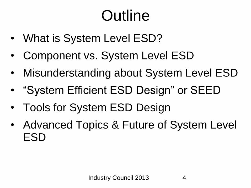
Outline
• What is System Level ESD?
• Component vs. System Level ESD
• Misunderstanding about System Level ESD
• “System Efficient ESD Design” or SEED
• Tools for System ESD Design
• Advanced Topics & Future of System Level ESD
4 Industry Council 2013
Outline
• What is System Level ESD?
• Component vs. System Level ESD
• Misunderstanding about System Level ESD
• “System Efficient ESD Design” or SEED
• Tools for System ESD Design
• Advanced Topics & Future of System Level ESD
5 Industry Council 2013

System Level ESD
• What is an ESD Event?
- Object becomes charged -> discharges to another
- Charging levels range from 1 V to 35,000 V
Discharge currents range from 1 A to 60 A or more
• What is a System Level ESD Event?
- An electrical system experiences an ESD Event
• What can happen in a System Level ESD Event?
- The system continues to work without problem
- The system experiences upset/lockup, but no physical
failure.
Typically referred to as “Soft Failure”
May or may not require user intervention
- The system experiences physical damage
Typically referred to as “Hard Failure”
6 Industry Council 2013
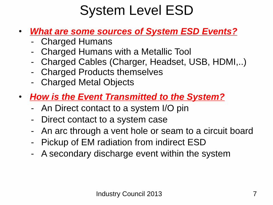
System Level ESD
• What are some sources of System ESD Events? - Charged Humans - Charged Humans with a Metallic Tool - Charged Cables (Charger, Headset, USB, HDMI,..) - Charged Products themselves - Charged Metal Objects
• How is the Event Transmitted to the System?
- An Direct contact to a system I/O pin
- Direct contact to a system case
- An arc through a vent hole or seam to a circuit board
- Pickup of EM radiation from indirect ESD
- A secondary discharge event within the system
7 Industry Council 2013

System Level ESD Testing
• System level ESD (qualification) testing is intended to ensure that finished products can continue normal operation during and after a system level ESD strike. - The IEC 61000-4-2 ESD Test Method is used to represent one
particular scenario of a charged human holding a metal object and discharging to a point on the system
- This is the most common test method used to assess the ESD robustness of the system
- Other test standards (e.g., ISO10605 for automotive, DO-160 for avionics) are used; depending on the application
• System Level ESD Test Results - Pass: System continues to work without interruption
- Soft error that corrects on itself
- Soft error requiring intervention (reboot, power cycle, …)
- Physical failure
8 Industry Council 2013

Categories of Failures (From Limited Case Studies)
• Common reported causes of system failure are:
- Charged Board Events (CBE)
- Cable Discharge Events (CDE)
- Electrical Overstress (EOS)
- IEC System Level ESD testing (for the “soft” failures, their relative
percentage could be higher)
9 Industry Council 2013

Outline
• What is System Level ESD?
• Component vs. System Level ESD
• Misunderstanding about System Level ESD
• “System Efficient ESD Design” or SEED
• Tools for System ESD Design
• Advanced Topics & Future of System Level ESD
10 Industry Council 2013
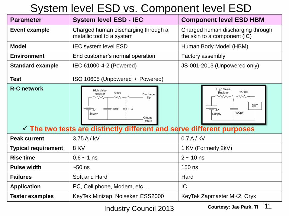
System level ESD vs. Component level ESD Parameter System level ESD - IEC Component level ESD HBM
Event example Charged human discharging through a metallic tool to a system
Charged human discharging through the skin to a component (IC)
Model IEC system level ESD Human Body Model (HBM)
Environment End customer’s normal operation Factory assembly
Standard example
Test
IEC 61000-4-2 (Powered)
ISO 10605 (Unpowered / Powered)
JS-001-2013 (Unpowered only)
R-C network
Peak current 3.75 A / kV 0.7 A / kV
Typical requirement 8 KV 1 KV (Formerly 2kV)
Rise time 0.6 ~ 1 ns 2 ~ 10 ns
Pulse width ~50 ns 150 ns
Failures Soft and Hard Hard
Application PC, Cell phone, Modem, etc… IC
Tester examples KeyTek Minizap, Noiseken ESS2000 KeyTek Zapmaster MK2, Oryx
The two tests are distinctly different and serve different purposes
Courtesy: Jae Park, TI 11 Industry Council 2013

Waveforms of Component HBM and System Level
4kV-HBM(schematic)
4kV-GUN
4kV-HBM(schematic)
4kV-GUN
4kV-HBM(schematic)
4kV-GUN
Time t [ns]
Cu
rre
nt I [A
]
Discharge current thru a 2-Ohm load
C = 100 pF, R = 1500 Ohm
• System level ESD gun test has
to be performed under
powered conditions
• For powered systems there are
two failure mechanisms - Destructive fail - Functional/Operational fail
• Improving the component ESD
levels will not solve this issue
• There is no clear correlation of
system level performance to
the HBM robustness
4 kV HBM is not the same as 4 kV System Level IEC!
Industry Council 2013 12
Note the extreme initial I(peak) due to the direct capacitive coupling with the gun tip
4kV IEC

Component Vs. System Test Result Correlation
• Case studies A through G represent data on products which had failure
voltages characterized for both HBM and IEC based system level test.
• Data indicates no correlation of HBM failure voltage to IEC failure voltage.
• This disparity between the two test methods is due to the fundamental differences in the stress waveforms and in the way the stress is applied during the tests
13 Industry Council 2013

“Improving the component ESD levels would not improve
the system level ESD performance.”
Following this, since ICs are now designed for lower
component ESD levels, why would this not be reflected by a
sudden change in the overall health of a system for its ESD
capability?
• The overall health of a system is dependent on a
comprehensive approach to the protection methodology
that includes a number of factors including on board
protection components, optimized board signal routing,
component packaging and, as a last line of defense, the
component level protection.
14 Industry Council 2013
Understanding System Level ESD Protection

Outline
• What is System Level ESD?
• Component vs. System Level ESD
• Misunderstanding about System Level ESD
• “System Efficient ESD Design” or SEED
• Tools for System ESD Design
• Advanced Topics & Future of System Level ESD
15 Industry Council 2013
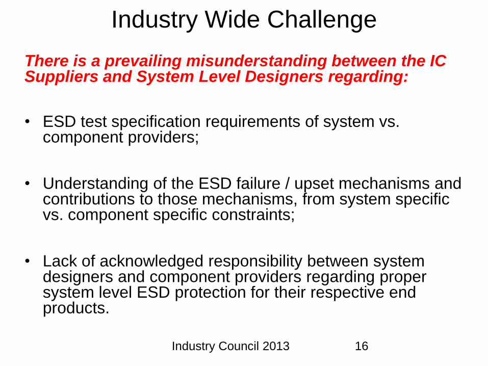
Industry Wide Challenge
There is a prevailing misunderstanding between the IC Suppliers and System Level Designers regarding:
• ESD test specification requirements of system vs. component providers;
• Understanding of the ESD failure / upset mechanisms and contributions to those mechanisms, from system specific vs. component specific constraints;
• Lack of acknowledged responsibility between system designers and component providers regarding proper system level ESD protection for their respective end products.
16 Industry Council 2013

Is 2kV "HBM" testing the same as IEC Zap Gun testing? • Unfortunately, there is sometimes confusion in the
comparison of the two methods. • Actual human contact to an IC component is simulated /
tested with the Human Body Model Tester, which results in ESD stress between two or more component pins.
• This is completely different from the IEC Test method
where the Zap Gun is used to test a system case, board or board connector and may or may not stress an IC.
17 Industry Council 2013
Industry Wide Challenge

Outline
• What is System Level ESD?
• Component vs. System Level ESD
• Misunderstanding about System Level ESD
• “System Efficient ESD Design” or SEED
• Tools for System ESD Design
• Advanced Topics & Future of System Level ESD
18 Industry Council 2013

System Efficient ESD Design
Industry Council 2013
• For efficient system ESD design, the Internal versus the
External pins must first be defined
• The interaction from the external pin stress to the
internal pin must then be analyzed
• Both Internal Pins and External Pins should meet
minimum HBM and CDM levels as defined by
component handling requirements; however, this is not
a system requirement
• For achieving system level ESD robustness, the External
Pins must be designed with a proper system protection
strategy; which is independent of their HBM/CDM
protection levels
19

busc
on
ne
cto
r
Printed
Circuit
BoardIC
IC
IC
IC
busc
on
ne
cto
r
Printed
Circuit
BoardIC
IC
IC
IC
Industry Council 2013
Differentiation of Internal Vs. External Pins
20
Circuit Board System
Internal External Stress Access to External Pins
• As identified here all the external pins are stressed with the IEC pulses
• What is the interaction to the corresponding interface pins?

Designing for the Overall System
• Internal Pins and External Pins should
meet minimum HBM and CDM levels as
defined by component handling
requirements
• System ESD protection design involves
an understanding of the system,
independent of component ESD levels
21 Industry Council 2013

Industry Council 2013
Do all pins on a device need to be tested using system
level events?
• Only the external pins (e.g. USB data lines, Vbus line, ID and other
control lines; codec, and battery pins, etc) need to be tested if the IC
is not protected with on-board components. However, if the pin is
protected by on-board components, TLP characterization of the pin is
more useful.
• Other internal ESD sensitive pins (e.g. control pins, reset pins, and
high speed data lines, etc.) can be inductively coupled during a
discharge to the case and/or to an adjacent trace of an exposed pin
undergoing system testing.
• These sensitive internal pins need to be identified and may need to
be monitored during system level events.
22
System-Efficient ESD Design (SEED) Concept
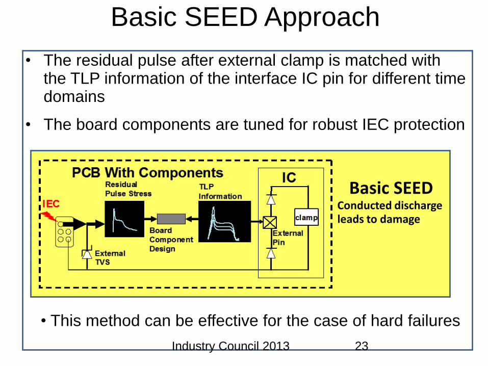
Basic SEED Approach
Basic SEED Conducted discharge leads to damage
• The residual pulse after external clamp is matched with the TLP information of the interface IC pin for different time domains
• The board components are tuned for robust IEC protection
• This method can be effective for the case of hard failures
Industry Council 2013 23

USB2 Interface Example with SEED
• 4 Pins to be protected ( D+,D-,ID,VBUS)
• High Speed Data Rate (480Mbit/s)
• EMI/ IEC ESD and Signal Integrity requirements
CFB
GND ID
D+ D-
VBUS
C2Power IC
usb2_otg_dp
usb2_otg_dm
ID
VBUS
OMAP ICCMF
TVS
C1
Receptacle
C3
VCC pin
TVS*
Transient Voltage
Suppressor
24

Summary of Basic SEED (I)
• It is often misunderstood that a high level of HBM ESD protection will adequately protect a component from IEC testing
• Even pins with >10kV HBM may not survive 3kV IEC
• Thus the external TVS plays a major role; however, the TVS alone would not still guarantee that the 8kV IEC requirement will be met
• A detailed simulation approach with understanding of the role of the various elements on the board becomes essential for achieving effective protection
Industry Council 2013 25

Advanced SEED
• System ESD can impact an entire system and can create both “hard” and “soft” failures.
• So called soft failures may involve complex EMC/EMI effects and also some Transient Latchup (TLU) phenomena.
• These issues require recommendations for component and system level manufacturers regarding proper protection / controls and best practice ESD design for EMC/EMI
Industry Council 2013 26
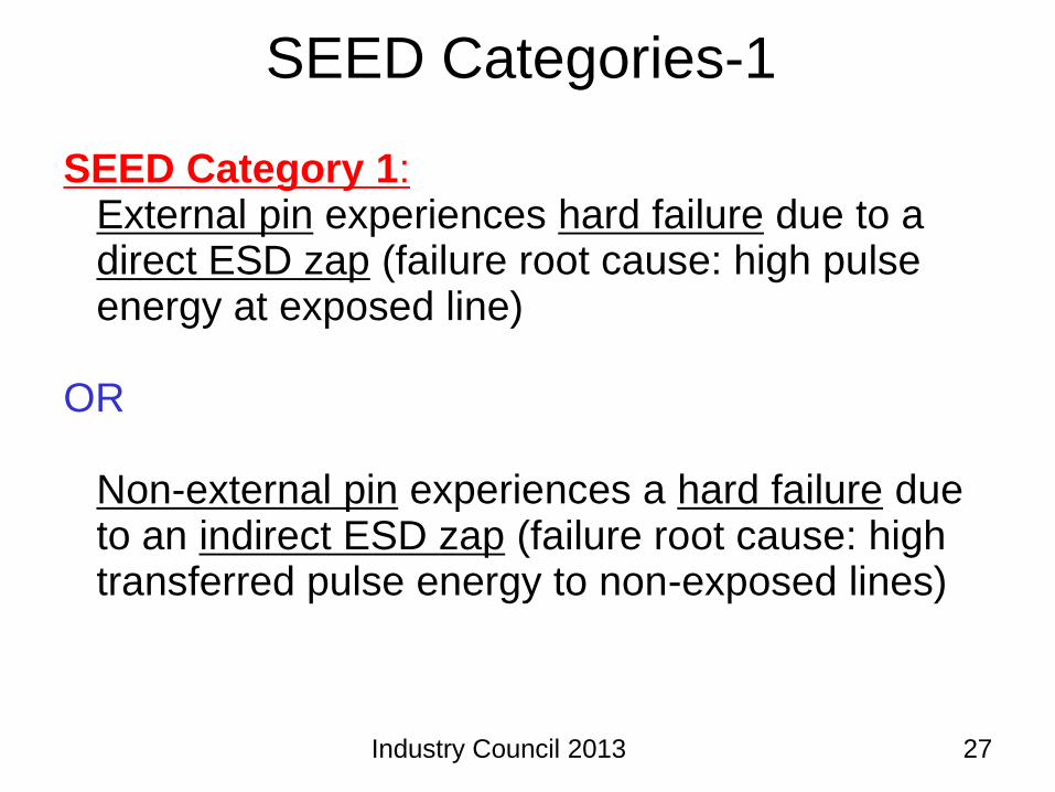
SEED Category 1: External pin experiences hard failure due to a direct ESD zap (failure root cause: high pulse energy at exposed line)
OR
Non-external pin experiences a hard failure due to an indirect ESD zap (failure root cause: high transferred pulse energy to non-exposed lines)
SEED Categories-1
Industry Council 2013 27

SEED Category 2: Pin experiences a transient latch-up event which can lead to either a hard or soft failure (failure root cause: current injection into the substrate which is too high)
SEED Categories-2,3
Industry Council 2013 28
SEED Category 3:
Describes protection of an IC experiencing soft failure due to low amplitude transient bursts in the system during an ESD zap (for example, this may be caused by degraded signal integrity of an exposed line, cross-talk to a neighboring line or supply noise).

Summary of SEED Options
Categories Strategy Comments
SEED 1 System ESD simulation using TLP characterization
Also requires analysis of the PCB trace elements
SEED 2 and SEED 3
Use EMC best design methods
Also requires detailed analysis of PCB behavior and EM scanning tools
Industry Council 2013 29

Outline
• What is System Level ESD?
• Component vs. System Level ESD
• Misunderstanding about System Level ESD
• “System Efficient ESD Design” or SEED
• Tools for System ESD Design
• Advanced Topics & Future of System Level ESD
30 Industry Council 2013

Basic Vs Extended SEED
Basic SEED Conducted discharge leads to damage
Extended SEED Covers also soft fails due to low injected currents and EM radiation
Industry Council 2013 31
Simulations must include analysis of the PCB trace elements
Needs additional EM scanning tools

Discharge via wired network connected to PCB port
Off-Chip Protection is the ideal approach! Industry Council 2013
32

Outline
• What is System Level ESD?
• Component vs. System Level ESD
• Misunderstanding about System Level ESD
• “System Efficient ESD Design” or SEED
• Tools for System ESD Design
• Advanced Topics & Future of System Level ESD
33 Industry Council 2013

• Coupling of ESD into Systems and Circuits
- How Does ESD Couple into a System and Affect a Specific Device During System Level Testing?
- What Happens When the Charge Gets into the System?
- Recoverable or “Soft” System Failure Modes
- System Degradation
- Hard System Level Failure Modes
Industry Council 2013 34
Advanced Topics (in JEP162)

• ESD/EMI Budget Strategy (Tradeoff Gamut
examples)
• Equipment Ground (Exit for the Pulse)
• Quick Fixes (Copper tape, upgrading
components)
• Information Available to the Designer
(Conflicting datasheets)
Industry Council 2013 35
Advanced Topics (in JEP162)

• Primary Goals of ESD/EMI Co-design Today
• Sufficient Signal Integrity and Functionality
• Adequate ESD/EMI Robustness and Compliance
• Cost and Time to Market
Industry Council 2013 36
Advanced Topics (in JEP162)

DSP and Microprocessors
• SerDes: 20 GB/sec at 20nm - Internal
• DDR:2.3G at 28nm - Internal
• USB and HDMI - External
• RF Antenna low tolerance to capacitance - External
The external pins require special attention for all future system level
ESD designs
Industry Council 2013 37
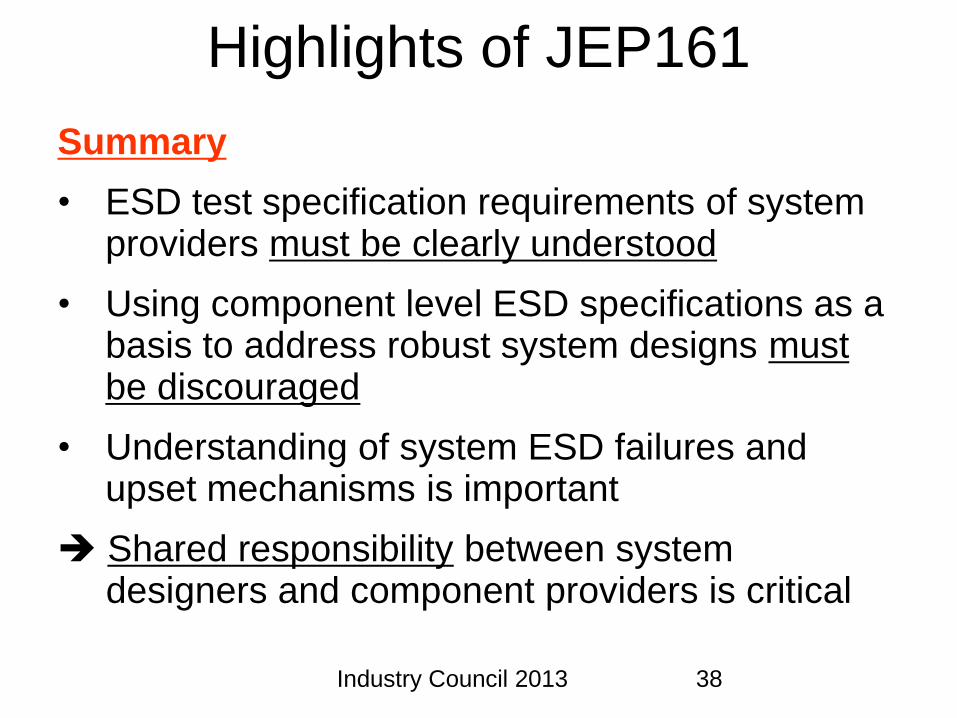
Summary
• ESD test specification requirements of system providers must be clearly understood
• Using component level ESD specifications as a basis to address robust system designs must be discouraged
• Understanding of system ESD failures and upset mechanisms is important
Shared responsibility between system designers and component providers is critical
38 Industry Council 2013
Highlights of JEP161
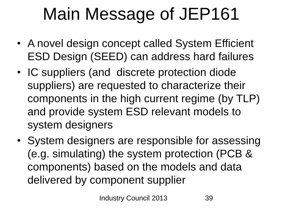
• A novel design concept called System Efficient
ESD Design (SEED) can address hard failures
• IC suppliers (and discrete protection diode
suppliers) are requested to characterize their
components in the high current regime (by TLP)
and provide system ESD relevant models to
system designers
• System designers are responsible for assessing
(e.g. simulating) the system protection (PCB &
components) based on the models and data
delivered by component supplier
Industry Council 2013 39
Main Message of JEP161
Recommended