SQFlash Industrial Class 10 Micro SD Card
Specifications subject to change without notice, contact your sales representatives for the most update information.
REV 0.3 Page 1 of 22 May 4, 2016
SQFlash Micro SD Card Technical Manual
Class 10 (SQF-MSDx1-xM/G-21x)

SQFlash Industrial Class 10 Micro SD Card
Specifications subject to change without notice, contact your sales representatives for the most update information.
REV 0.3 Page 2 of 22 May. 4, 2016
CONTENTS 1.Overview ............................................................................................ 42.Standard Features ............................................................................. 53.Additional Features ........................................................................... 64.Pin Assignment and Block Diagram ................................................ 85.Power Consumption ....................................................................... 116.DC Characters ................................................................................. 117.AC Characters ................................................................................. 148.Dimensions ...................................................................................... 19Appendix: Part Number Table ........................................................... 21

SQFlash Industrial Class 10 Micro SD Card
Specifications subject to change without notice, contact your sales representatives for the most update information.
REV 0.3 Page 3 of 22 May. 4, 2016
Revision History
Rev. Date History
0.1 2014/8/4 1. 1st draft
0.2 2014/8/21 1. Add Ultra MLC
0.3 2016/5/4 1. Add SLC
Advantech reserves the right to make changes without further notice to any products or data herein to improve reliability, function, or
design. Information furnished by Advantech is believed to be accurate and reliable. However, Advantech does not assure any liability
arising out of the application or use of this information, nor the application or use of any product or circuit described herein, neither
does it convey any license under its patent rights nor the rights of others.
Copyright © 1983-2015 Advantech Co., Ltd. All rights reserved.

SQFlash Industrial Class 10 Micro SD Card
Specifications subject to change without notice, contact your sales representatives for the most update information.
REV 0.3 Page 4 of 22 May. 4, 2016
1. Overview
The SQFlash Micro Secure Digital card (SQF-MSD) is fully compliant to the specification released by SD Card
Association. The Command List supports [Part 1 Physical Layer Specification Ver3.01 Final] definitions. Card
Capacity of Non-secure Area, Secure Area Supports [Part 3 Security Specification Ver3.00 Final] specifications.
The microSD 3.0 card comes with 8-pin interface, designed to operate at a maximum operating frequency of
50MHz or 100MHz. It can alternate communication protocol between the SD mode and SPI mode. It performs data
error detection and correction with very low power consumption. Its capacity could be more than 128MB and up to
64GB.
SQFlash Industrial Micro SD card is one of the most popular cards today based on its high performance, good
reliability and wide compatibility. Not to mention that it’s well adapted for hand-held applications in
semi-industrial/medical markets already.
SQFlash Industrial Class 10 Micro SD Card
Specifications subject to change without notice, contact your sales representatives for the most update information.
REV 0.3 Page 5 of 22 May. 4, 2016
2. Standard Features
Support SD system specification version 3.0
Card capacity of non-secure area and secure area support [Part 3 Security Specification Ver3.0 Final] Specifications
Support SD SPI mode
Designed for read-only and read/write cards
Bus Speed Mode (using 4 parallel data lines)
– UHS-I mode
SDR12 - SDR up to 25MHz 1.8V signaling
SDR25 - SDR up to 50MHz 1.8V signaling
SDR50: 1.8V signaling, Frequency up to 100 MHz, up to 50MB/sec
SDR104: 1.8V signaling, Frequency up to 208MHz, up to 104MB/sec
DDR50: 1.8V signaling, Frequency up to 50 MHz, sampled on both clock edges, up to 50MB/sec
Note: Timing in 1.8V signaling is different from that of 3.3V signaling.
The command list supports [Part 1 Physical Layer Specification Ver3.1 Final] definitions
Copyrights Protection Mechanism
– Compliant with the highest security of SDMI standard
Support CPRM (Content Protection for Recordable Media) of SD Card
Card removal during read operation will never harm the content
Password Protection of cards (optional)
Write Protect feature using mechanical switch
Built-in write protection features (permanent and temporary)
+4KV/-4KV ESD protection in contact pads
Operation voltage range: 2.7 ~ 3.6V

SQFlash Industrial Class 10 Micro SD Card
Specifications subject to change without notice, contact your sales representatives for the most update information.
REV 0.3 Page 6 of 22 May. 4, 2016
3. Additional Features
Capacities – SLC type : 128MB,256MB,512MB,1GB,2GB
– MLC type:4GB,8GB,16GB,32GB,64GB
– Ultra MLC type:2GB,4GB,8GB,16GB,32GB
Flash type – 24 nm SLC
– A19 nm MLC
Performance (SLC)
Capacity Mode Sequential
Read (MB/s) Write (MB/s)
128MB Non-UHS 16 4 256MB Non-UHS 16 10 512MB Non-UHS 16 10
1GB Non-UHS 18 10 2GB Non-UHS 20 20
Performance (MLC)
Capacity Mode Sequential
Read (MB/s) Write (MB/s)
2GB UHS-I 90 20 4GB UHS-I 90 20 8GB UHS-I 90 30
16GB UHS-I 90 40 32GB UHS-I 90 40 64GB UHS-I 90 45
Temperature Ranges – Normal Temperature
-25 to 85
– Industrial Temperature
-40 to 85
Mechanical Specification – Shock:1,500G, Peak / 0.5ms
– Vibration:20G, Peak / 20~2000Hz
– Drop: 1.5m free fall
– Bending: ≥ 10N, hold 1min / 5times
– Torque: 0.15N-m or +/-2.5deg
– Salt Spray:
Concentration: 3% NaCl
Temperature: 35
Storage for 24 HRS
– Waterproof: JIS IPX7 compliance
Humidity – Operating Humidity:5% ~ 93%
– Non-Operating Humidity:5% ~ 93%
SQFlash Industrial Class 10 Micro SD Card
Specifications subject to change without notice, contact your sales representatives for the most update information.
REV 0.3 Page 7 of 22 May. 4, 2016
NAND flash Data Retention – 10 years

SQFlash Industrial Class 10 Micro SD Card
Specifications subject to change without notice, contact your sales representatives for the most update information.
REV 0.3 Page 8 of 22 May. 4, 2016
4. Flash Management
Error Correction Code (ECC) Flash memory cells will deteriorate with use, which might generate random bit errors in the stored data. Thus, SQF-MSD applies the BCH ECC algorithm, which can detect and correct errors occur during read process, ensure data been read correctly, as well as protect data from corruption.
Wear Leveling NAND Flash devices can only undergo a limited number of program/erase cycles, and in most cases, the flash media are not used evenly. If some area get updated more frequently than others, the lifetime of the device would be reduced significantly. Thus, Wear Leveling technique is applied to extend the lifespan of NAND Flash by evenly distributing write and erase cycles across the media. SQF-MSD provides advanced Wear Leveling algorithm, which can efficiently spread out the flash usage through the whole flash media area. Moreover, by implementing both dynamic and static Wear Leveling algorithms, the life expectancy of the NAND Flash is greatly improved.
Bad Block Management Bad blocks are blocks that include one or more invalid bits, and their reliability is not guaranteed. Blocks that are identified and marked as bad by the manufacturer are referred to as “Initial Bad Blocks”. Bad blocks that are developed during the lifespan of the flash are named “Later Bad Blocks”. SQF-MSD implements an efficient bad block management algorithm to detect the factory-produced bad blocks and manages any bad blocks that appear with use. This practice further prevents data being stored into bad blocks and improves the data reliability.
Auto-Read Refresh Auto-Read Refresh is specifically applied on devices that read data mostly but rarely write data, such as GPS. When blocks are continuously read, then the device cannot activate wear leveling since it can only be applied while writing data. Thus, errors will accumulate and become uncorrectable. Accordingly, to avoid errors exceed the amount ECC can correct and blocks turn bad, The firmware of SQF-MSD will automatically refresh the bit errors when the error number in one block approaches the threshold, ex., 24 bits.

SQFlash Industrial Class 10 Micro SD Card
Specifications subject to change without notice, contact your sales representatives for the most update information.
REV 0.3 Page 9 of 22 May. 4, 2016
Endurance JEDEC defined an endurance rating TBW (TeraByte Written), following by the equation below, for indicating the number of terabytes a flash drive can be written which is a measurement of flash drive’s expected lifespan, represents the amount of data written to the device.
TBW = [(NAND Endurance) x (Flash Drive Capacity)] / WAF
NAND Endurance: Program / Erase cycle of a NAND flash. o SLC: 60,000 cycles o Ultra MLC: 20,000 cycles o MLC: 3,000 cycles
Flash Drive Capacity: Physical capacity in total of a Flash Drive. WAF: Write Amplification Factor (WAF), as the equation shown below, is a numerical value
representing the ratio between the amount of data that a flash drive controller needs to write and the amount of data that the host’s flash controller writes. A better WAF, which is near to 1, guarantees better endurance and lower frequency of data written to flash memory.
WAF = (Lifetime write to flash) / (Lifetime write to host)
The TBW rating for a flash drive shall be derived for and verified under the following workload conditions,
Sequential Write (copy file into card) P/E cycles incurred: erase count after writing – erase count before writing
SQFlash Micro SD Card TBW
capacity TBW
WAF SLC WAF Ultra MLC MLC
128 MB
1.024414
7 -- -- --
256 MB 14 -- -- --
1 GB 58 -- -- --
2 GB 117
1.0301339
39 --
4 GB 234 77 11
8 GB 469 155 23
16 GB 937 310 47
32 GB 1874 621 93
64 GB -- -- 1243 186
128 GB -- -- -- 372
SQFlash Industrial Class 10 Micro SD Card
Specifications subject to change without notice, contact your sales representatives for the most update information.
REV 0.3 Page 10 of 22 May. 4, 2016
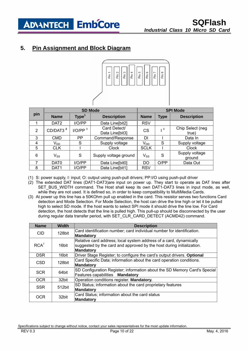
5. Pin Assignment and Block Diagram
pin SD Mode SPI Mode
Name Type1 Description Name Type Description
1 DAT2 I/O/PP Data Line[bit2] RSV
2 CD/DAT3 2 I/O/PP 3 Card Detect/ Data Line[bit3]
CS I 3 Chip Select (neg true)
3 CMD PP Command/Response DI I Data In 4 VDD S Supply voltage VDD S Supply voltage 5 CLK I Clock SCLK I Clock
6 VSS S Supply voltage ground VSS S Supply voltage
ground 7 DAT0 I/O/PP Data Line[bit0] DO O/PP Data Out 8 DAT1 I/O/PP Data Line[bit1] RSV
(1) S: power supply, I: input; O: output using push-pull drivers; PP:I/O using push-pull driver (2) The extended DAT lines (DAT1-DAT3)are input on power up. They start to operate as DAT lines after
SET_BUS_WIDTH command. The Host shall keep its own DAT1-DAT3 lines in input mode, as well, while they are not used. It is defined so, in order to keep compatibility to MultiMedia Cards.
(3) At power up this line has a 50KOhm pull up enabled in the card. This resistor serves two functions Card detection and Mode Selection. For Mode Selection, the host can drive the line high or let it be pulled high to select SD mode. If the host wants to select SPI mode it should drive the line low. For Card detection, the host detects that the line is pulled high. This pull-up should be disconnected by the user during regular data transfer period, with SET_CLR_CARD_DETECT (ACMD42) command.
Name Width Description
CID 128bit Card identification number; card individual number for identification. Mandatory
RCA1 16bit Relative card address; local system address of a card, dynamically suggested by the card and approved by the host during initialization. Mandatory
DSR 16bit Driver Stage Register; to configure the card’s output drivers. Optional
CSD 128bit Card Specific Data; information about the card operation conditions. Mandatory
SCR 64bit SD Configuration Register; information about the SD Memory Card's Special Features capabilities Mandatory
OCR 32bit Operation conditions register. Mandatory.
SSR 512bit SD Status; information about the card proprietary features Mandatory
OCR 32bit Card Status; information about the card status Mandatory
SQFlash Industrial Class 10 Micro SD Card
Specifications subject to change without notice, contact your sales representatives for the most update information.
REV 0.3 Page 11 of 22 May. 4, 2016
6. Power Consumption
Table list as below is the power consumption of SQF-MSD card with different type of flash memory. Capacity Flash Structure Read Write Idle
4GB 4GB x 1 100 100 150 8GB 8GB x 1 100 100 150
16GB 8GB x 2 150 150 180 32GB 8GB x 4 180 180 220 64GB 8GB x 8 200 200 250
(1) Data transfer mode is single channel.
7. Electrical Specifications Absolute Maximum Rating
Item Symbol Parameter MIN MAX Unit 1 VDD-VSS DC Power Supply -0.3 +3.3 V 2 VIN Input Voltage VSS-0.3 VDD+0.3 V 3 Ta Operating Temperature (Gold) -25 +85 4 Ta Operating Temperature (Diamond) -40 +85 5 Tst Storage Temperature -40 +85 6 VDD VDD Voltage 2.7 3.6 V
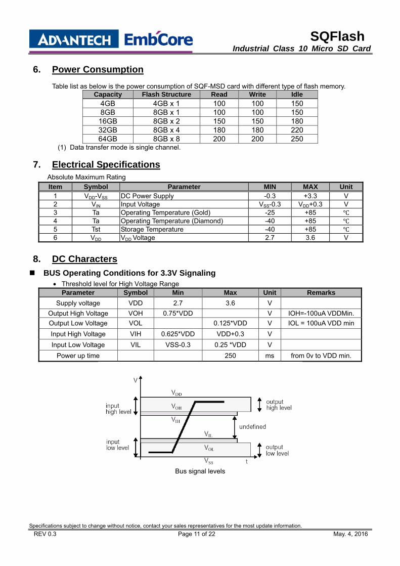
8. DC Characters
BUS Operating Conditions for 3.3V Signaling Threshold level for High Voltage Range
Parameter Symbol Min Max Unit Remarks
Supply voltage VDD 2.7 3.6 V
Output High Voltage VOH 0.75*VDD V IOH=-100uA VDDMin.
Output Low Voltage VOL 0.125*VDD V IOL = 100uA VDD min
Input High Voltage VIH 0.625*VDD VDD+0.3 V
Input Low Voltage VIL VSS-0.3 0.25 *VDD V
Power up time 250 ms from 0v to VDD min.
Bus signal levels
SQFlash Industrial Class 10 Micro SD Card
Specifications subject to change without notice, contact your sales representatives for the most update information.
REV 0.3 Page 12 of 22 May. 4, 2016
Peak Voltage and Leakage Current Parameter Symbol Min Max Unit Remarks
Peak voltage on all lines -0.3 VDD+0.3 V
All Inputs Input Leakage Current -10 10 uA
All Outputs Output Leakage Current -10 10 uA
Bus Signal Line Levels
Parameter symbol Min Max Unit Remark
Pull-up resistance RCMD
RDAT 10 100 kΩ to prevent bus floating
Total bus capacitance for each signal line
CL 40 pF 1 card CHOST+CBUS shall not exceed 30 pF
Capacitance of the card for each signal pin
CCARD
10 pF
Maximum signal line inductance 16 nH fpp<20 MHz
Pull-up resistance inside card (pin1) RDAT3
10 90 kΩ May be used for card detection
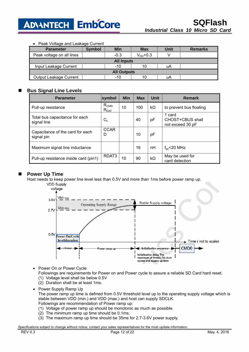
Power Up Time Host needs to keep power line level less than 0.5V and more than 1ms before power ramp up.
Power On or Power Cycle
Followings are requirements for Power on and Power cycle to assure a reliable SD Card hard reset. (1) Voltage level shall be below 0.5V (2) Duration shall be at least 1ms.
Power Supply Ramp Up The power ramp up time is defined from 0.5V threshold level up to the operating supply voltage which is stable between VDD (min.) and VDD (max.) and host can supply SDCLK. Followings are recommendation of Power ramp up: (1) Voltage of power ramp up should be monotonic as much as possible. (2) The minimum ramp up time should be 0.1ms. (3) The maximum ramp up time should be 35ms for 2.7-3.6V power supply.
SQFlash Industrial Class 10 Micro SD Card
Specifications subject to change without notice, contact your sales representatives for the most update information.
REV 0.3 Page 13 of 22 May. 4, 2016
Power Down and Power Cycle (1) When the host shuts down the power, the card VDD shall be lowered to less than 0.5Volt for a
minimum period of 1ms. During power down, DAT, CMD, and CLK should be disconnected or driven to logical 0 by the host to avoid a situation that the operating current is drawn through the signal lines.
(2) If the host needs to change the operating voltage, a power cycle is required. Power cycle means the power is turned off and supplied again. Power cycle is also needed for accessing cards that are already in Inactive State. To create a power cycle the host shall follow the power down description before power up the card (i.e. the card VDD shall be once lowered to less than 0.5Volt for a minimum period of 1ms).
SQFlash Industrial Class 10 Micro SD Card
Specifications subject to change without notice, contact your sales representatives for the most update information.
REV 0.3 Page 14 of 22 May. 4, 2016
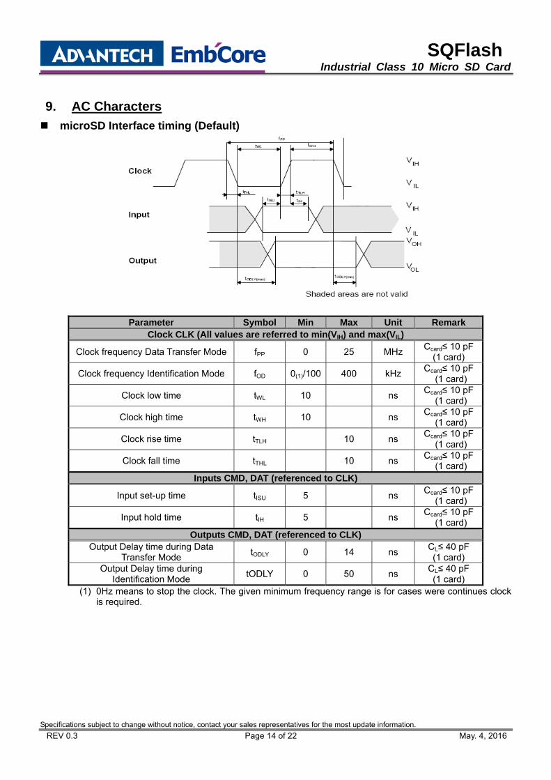
9. AC Characters
microSD Interface timing (Default)
Parameter Symbol Min Max Unit Remark Clock CLK (All values are referred to min(VIH) and max(VIL)
Clock frequency Data Transfer Mode fPP 0 25 MHz Ccard≤ 10 pF
(1 card)
Clock frequency Identification Mode fOD 0(1)/100 400 kHz Ccard≤ 10 pF
(1 card)
Clock low time tWL 10 ns Ccard≤ 10 pF
(1 card)
Clock high time tWH 10 ns Ccard≤ 10 pF
(1 card)
Clock rise time tTLH 10 ns Ccard≤ 10 pF
(1 card)
Clock fall time tTHL 10 ns Ccard≤ 10 pF
(1 card) Inputs CMD, DAT (referenced to CLK)
Input set-up time tISU 5 ns Ccard≤ 10 pF
(1 card)
Input hold time tIH 5 ns Ccard≤ 10 pF
(1 card) Outputs CMD, DAT (referenced to CLK)
Output Delay time during Data Transfer Mode
tODLY 0 14 ns CL≤ 40 pF (1 card)
Output Delay time during Identification Mode
tODLY 0 50 ns CL≤ 40 pF (1 card)
(1) 0Hz means to stop the clock. The given minimum frequency range is for cases were continues clock is required.
SQFlash Industrial Class 10 Micro SD Card
Specifications subject to change without notice, contact your sales representatives for the most update information.
REV 0.3 Page 15 of 22 May. 4, 2016
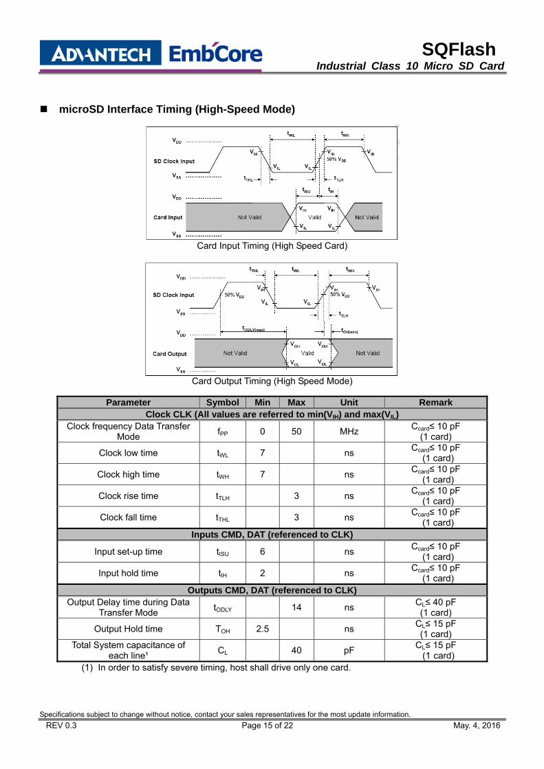
microSD Interface Timing (High-Speed Mode)
Card Input Timing (High Speed Card)
Card Output Timing (High Speed Mode)
Parameter Symbol Min Max Unit Remark Clock CLK (All values are referred to min(VIH) and max(VIL)
Clock frequency Data Transfer Mode
fPP 0 50 MHz Ccard≤ 10 pF
(1 card)
Clock low time tWL 7 ns Ccard≤ 10 pF
(1 card)
Clock high time tWH 7 ns Ccard≤ 10 pF
(1 card)
Clock rise time tTLH 3 ns Ccard≤ 10 pF
(1 card)
Clock fall time tTHL 3 ns Ccard≤ 10 pF
(1 card) Inputs CMD, DAT (referenced to CLK)
Input set-up time tISU 6 ns Ccard≤ 10 pF
(1 card)
Input hold time tIH 2 ns Ccard≤ 10 pF
(1 card) Outputs CMD, DAT (referenced to CLK)
Output Delay time during Data Transfer Mode
tODLY 14 ns CL≤ 40 pF (1 card)
Output Hold time TOH 2.5 ns CL≤ 15 pF (1 card)
Total System capacitance of each line¹
CL 40 pF CL≤ 15 pF
(1 card) (1) In order to satisfy severe timing, host shall drive only one card.
SQFlash Industrial Class 10 Micro SD Card
Specifications subject to change without notice, contact your sales representatives for the most update information.
REV 0.3 Page 16 of 22 May. 4, 2016
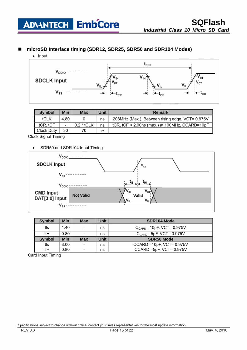
microSD Interface timing (SDR12, SDR25, SDR50 and SDR104 Modes) Input
Symbol Min Max Unit Remark
tCLK 4.80 0 ns 208MHz (Max.), Between rising edge, VCT= 0.975V
tCR, tCF - 0.2 * tCLK ns tCR, tCF < 2.00ns (max.) at 100MHz, CCARD=10pFClock Duty 30 70 %
Clock Signal Timing
SDR50 and SDR104 Input Timing
Symbol Min Max Unit SDR104 Mode
tls 1.40 - ns CCARD =10pF, VCT= 0.975V
tlH 0.80 - ns CCARD =5pF, VCT= 0.975V Symbol Min Max Unit SDR50 Mode
tls 3.00 - ns CCARD =10pF, VCT= 0.975V tlH 0.80 - ns CCARD =5pF, VCT= 0.975V
Card Input Timing
SQFlash Industrial Class 10 Micro SD Card
Specifications subject to change without notice, contact your sales representatives for the most update information.
REV 0.3 Page 17 of 22 May. 4, 2016
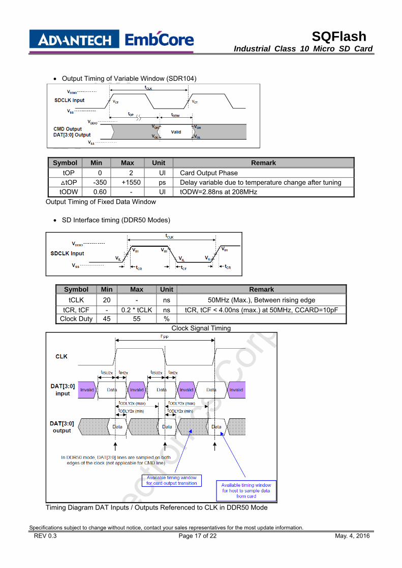
Output Timing of Variable Window (SDR104)
Symbol Min Max Unit Remark
tOP 0 2 Ul Card Output Phase
tOP -350 +1550 ps Delay variable due to temperature change after tuning
tODW 0.60 - Ul tODW=2.88ns at 208MHz
Output Timing of Fixed Data Window
SD Interface timing (DDR50 Modes)
Symbol Min Max Unit Remark
tCLK 20 - ns 50MHz (Max.), Between rising edge
tCR, tCF - 0.2 * tCLK ns tCR, tCF < 4.00ns (max.) at 50MHz, CCARD=10pF Clock Duty 45 55 %
Clock Signal Timing
Timing Diagram DAT Inputs / Outputs Referenced to CLK in DDR50 Mode
SQFlash Industrial Class 10 Micro SD Card
Specifications subject to change without notice, contact your sales representatives for the most update information.
REV 0.3 Page 18 of 22 May. 4, 2016
Parameter Symbol Min Max Unit Remark
Input CMD (referenced to CLK rising edge)
Input set-up time tISU 6 - ns Ccard≤ 10 pF
(1 card)
Input hold time tIH 0.8 - ns Ccard≤ 10 pF
(1 card) Output CMD (referenced to CLK rising edge)
Output Delay time during Data Transfer Mode
tODLY 13.7 ns Ccard≤ 30 pF
(1 card)
Output Hold time tOH 1.5 - ns Ccard≤ 10 pF
(1 card) Inputs DAT (referenced to CLK rising and falling edges)
Input set-up time tISU2X 3 - ns Ccard≤ 10 pF
(1 card)
Input hold time tIH2X 0.8 - ns Ccard≤ 10 pF
(1 card) Outputs CMD, DAT (referenced to CLK)
Output Delay time during Data Transfer Mode
tODLY2X - 7.0 ns CL≤ 25 pF (1 card)
Output Hold time tOH2X 1.5 - ns CL≥ 15 pF (1 card)
SQFlash Industrial Class 10 Micro SD Card
Specifications subject to change without notice, contact your sales representatives for the most update information.
REV 0.3 Page 19 of 22 May. 4, 2016
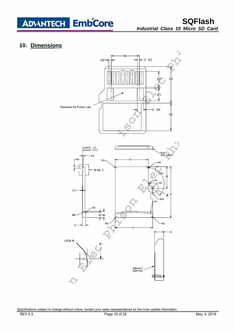
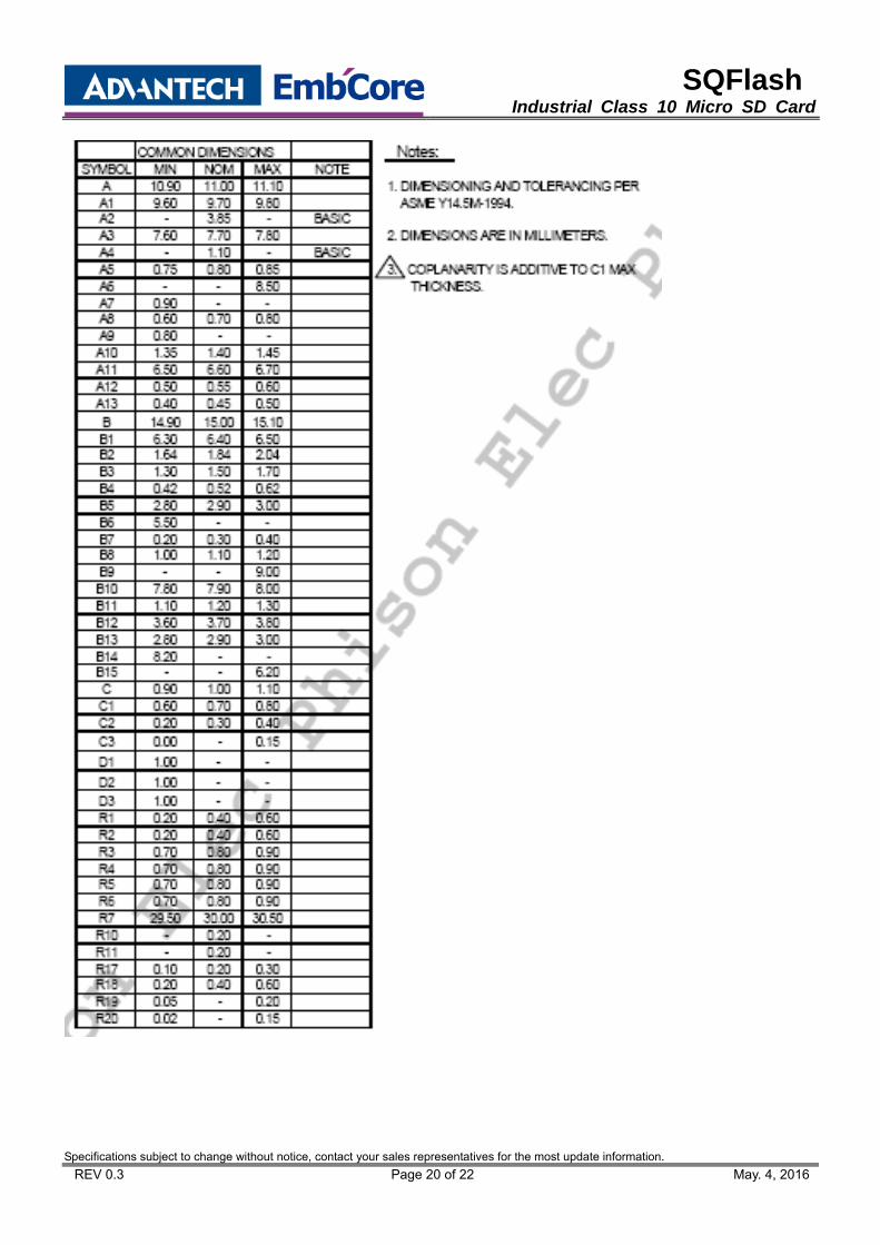
10. Dimensions
SQFlash Industrial Class 10 Micro SD Card
Specifications subject to change without notice, contact your sales representatives for the most update information.
REV 0.3 Page 20 of 22 May. 4, 2016
SQFlash Industrial Class 10 Micro SD Card
Specifications subject to change without notice, contact your sales representatives for the most update information.
REV 0.3 Page 21 of 22 May. 4, 2016
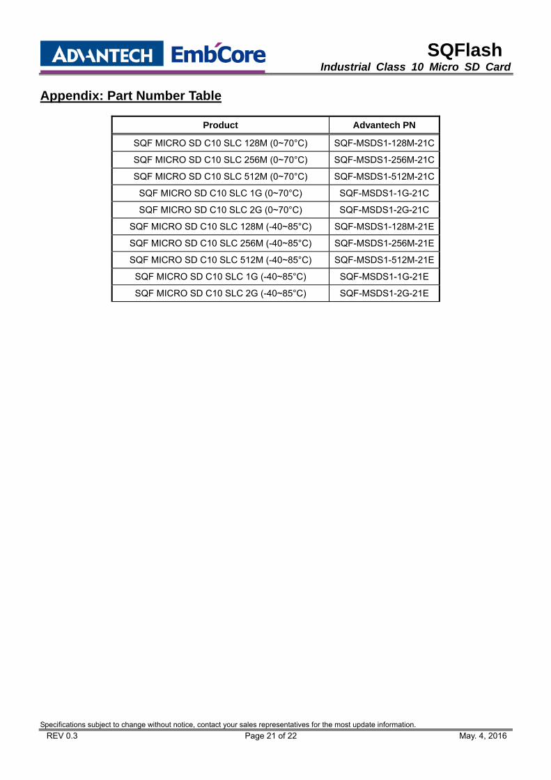
Appendix: Part Number Table
Product Advantech PN
SQF MICRO SD C10 SLC 128M (0~70°C) SQF-MSDS1-128M-21C
SQF MICRO SD C10 SLC 256M (0~70°C) SQF-MSDS1-256M-21C
SQF MICRO SD C10 SLC 512M (0~70°C) SQF-MSDS1-512M-21C
SQF MICRO SD C10 SLC 1G (0~70°C) SQF-MSDS1-1G-21C
SQF MICRO SD C10 SLC 2G (0~70°C) SQF-MSDS1-2G-21C
SQF MICRO SD C10 SLC 128M (-40~85°C) SQF-MSDS1-128M-21E
SQF MICRO SD C10 SLC 256M (-40~85°C) SQF-MSDS1-256M-21E
SQF MICRO SD C10 SLC 512M (-40~85°C) SQF-MSDS1-512M-21E
SQF MICRO SD C10 SLC 1G (-40~85°C) SQF-MSDS1-1G-21E
SQF MICRO SD C10 SLC 2G (-40~85°C) SQF-MSDS1-2G-21E

SQFlash Industrial Class 10 Micro SD Card
Specifications subject to change without notice, contact your sales representatives for the most update information.
REV 0.3 Page 22 of 22 May. 4, 2016
MLC Product Advantech PN
SQF MICRO SD C10 MLC 4G (-25~85°C) SQF-MSDM1-4G-21C
SQF MICRO SD C10 MLC 8G (-25~85°C) SQF-MSDM1-8G-21C
SQF MICRO SD C10 MLC 16G (-25~85°C) SQF-MSDM1-16G-21C
SQF MICRO SD C10 MLC 32G (-25~85°C) SQF-MSDM1-32G-21C
SQF MICRO SD C10 MLC 64G (-25~85°C) SQF-MSDM1-64G-21C
SQF MICRO SD C10 MLC 4G (-40~85°C) SQF-MSDM1-4G-21E
SQF MICRO SD C10 MLC 8G (-40~85°C) SQF-MSDM1-8G-21E
SQF MICRO SD C10 MLC 16G (-40~85°C) SQF-MSDM1-16G-21E
SQF MICRO SD C10 MLC 32G (-40~85°C) SQF-MSDM1-32G-21E
SQF MICRO SD C10 MLC 64G (-40~85°C) SQF-MSDM1-64G-21E
Ultra MLC
Product Advantech PN
SQF MICRO SD C10 UMLC 2G (-25~85°C) SQF-MSDU1-2G-21C
SQF MICRO SD C10 UMLC 4G (-25~85°C) SQF-MSDU1-4G-21C
SQF MICRO SD C10 UMLC 8G (-25~85°C) SQF-MSDU1-8G-21C
SQF MICRO SD C10 UMLC 16G (-25~85°C) SQF-MSDU1-16G-21C
SQF MICRO SD C10 UMLC 32G (-25~85°C) SQF-MSDU1-32G-21C
SQF MICRO SD C10 UMLC 2G (-40~85°C) SQF-MSDU1-2G-21E
SQF MICRO SD C10 UMLC 4G (-40~85°C) SQF-MSDU1-4G-21E
SQF MICRO SD C10 UMLC 8G (-40~85°C) SQF-MSDU1-8G-21E
SQF MICRO SD C10 UMLC 16G (-40~85°C) SQF-MSDU1-16G-21E
SQF MICRO SD C10 UMLC 32G (-40~85°C) SQF-MSDU1-32G-21E
Recommended


![PortableHDCar DVR - Masterpiece · 2015-01-13 · 2. Totakethe micro SD cardout, slightlypress the micro SD cardto eject it. [Note]: 1. Observe the direc on to insert the micro SD](https://img.dokumen.tips/doc/110x75/5f73f8bb2864981d0c7bb0d1/portablehdcar-dvr-2015-01-13-2-totakethe-micro-sd-cardout-slightlypress-the.jpg)