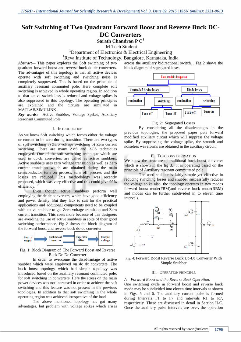
IJSRD - International Journal for Scientific Research & Development| Vol. 3, Issue 02, 2015 | ISSN (online): 2321-0613
All rights reserved by www.ijsrd.com 1796
Soft Switching of Two Quadrant Forward Boost and Reverse Buck DC-
DC Converters Sarath Chandran P C
1
1M.Tech Student
1Department of Electronics & Electrical Engineering
1Reva Institute of Technology, Bangalore, Karnataka, India
Abstract— This paper explores the Soft switching of two
quadrant forward boost and reverse buck dc dc converters.
The advantages of this topology is that all active devices
operate with soft switching and switching noise is
completely suppressed. This is based on the principle of
auxiliary resonant commuted pole. Here complete soft
switching is achieved in whole operating region. In addition
to that active switch loss is reduced and voltage spikes is
also suppressed in this topology. The operating principles
are explained and the circuits are simulated in
MATLAB/SIMULINK.
Key words: Active Snubber, Voltage Spikes, Auxiliary
Resonant Commuted Pole
I. INTRODUCTION
As we know Soft switching which forces either the voltage
or current to be zero during transition. There are two types
of soft switching a) Zero voltage switching b) Zero current
switching. There are many ZVS and ZCS techniques
employed. One of the soft switching technique which are
used in dc-dc converters are called as active snubbers.
Active snubbers uses zero voltage transition as well as Zero
current transition which are obtained during the main
semiconductor turn on process, turn off process and the
losses are reduced. This methodology was recently
proposed, which was very effective and this could give 99%
efficiency.
Even though active snubbers perform well
employing the dc dc converters, which have good efficiency
and power density. But they lack to suit for the practical
applications and additional components need to be coupled
with active snubber to get Zero voltage transition and Zero
current transition. This costs more because of this designers
are avoiding the use of active snubbers in spite of their good
switching performance. Fig 2 shows the block diagram of
the forward boost and reverse buck dc-dc converter
Fig. 1: Block Diagram of The Forward Boost and Reverse
Buck Dc-Dc Converter
In order to overcome the disadvantage of active
snubber which were employed on dc dc converters. The
buck boost topology which had simple topology was
introduced based on the auxiliary resonant commuted pole,
for soft switching in converters. Here the stress on the main
power devices was not increased in order to achieve the soft
switching and this feature was not present in the previous
topologies. In addition to that soft switching in the whole
operating region was achieved irrespective of the load
The above mentioned topology has got many
advantages, but problem with voltage spikes which arises
across the auxiliary bidirectional switch. . Fig 2 shows the
block diagram of segregated loses.
Fig. 2: Segregated Losses
By considering all the disadvantages in the
previous topologies, the proposed paper puts forward
modified auxiliary circuit which will suppress the voltage
spike. By suppressing the voltage spike, the smooth and
noiseless waveforms are obtained in the auxiliary circuit.
II. TOPOLOGY DERIVATION
We know the structure of traditional buck boost converter
which is shown in the fig 3. it is operating based on the
principle of Auxiliary resonant commutated pole
The used snubber is fairly simple yet effective in
reducing switching losses and snubber successfully reduces
the voltage spike also. the topology operates in two modes
forward boost mode(FBM)and reverse buck mode(RBM)
and modes can be further subdivided in to eleven time
intervals.
Fig. 4: Forward Boost Reverse Buck Dc-Dc Converter With
Simple Snubber
III. OPERATION PRINCIPLE
A. Forward Boost and the Reverse Buck Operation:
One switching cycle in forward boost and reverse buck
mode may be subdivided into eleven time intervals as shown
in Figs. 5 and 6. The auxiliary current pulse is formed
during Intervals F1 to F7 and intervals R1 to R7,
respectively. These are discussed in detail in Section II-C.
Once the auxiliary pulse intervals are over, the operation

Soft Switching of Two Quadrant Forward Boost and Reverse Buck DC-DC Converters
(IJSRD/Vol. 3/Issue 02/2015/444)
All rights reserved by www.ijsrd.com 1797
continues by main circuit intervals shown in Fig. 4 and
discussed below.
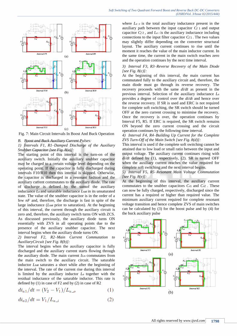
1) Interval F9 and R9–t6 < t < t7–Storing Energy in the
Main Inductor Lm [see Fig. 7(a)]:
This interval is a standard interval present in conventional
hard switched converters. The main current flows from the
energy source through the main inductor Lm and the main
switch. The main energy portion is stored in Lm during this
interval. Duration of this interval defines the difference
between the output and input voltage. The duration is often
controlled by the voltage controller and the interval ends by
turning OFF the main switch.
2) Interval F10 and R10–t7 < t < t8–ZVS Turn-Off of the
Main Switch [see Fig. 7(b)]:
When the main switch turns OFF, the current ILm
commutates almost instantly to the capacitors Cs1 and Cs2 .
These capacitors serve as turn-off snubber slowing down the
voltage change across the main switches, effectively
resulting in ZVS turn-off. The snubber capacitors are
charged, respectively, discharged by the main current. The
interval ends when the charge/discharge cycle is completed.
In that moment ,the main diode turns ON and the next
interval begins. The auxiliary switch is turned OFF during
Interval F9/R9. The turn-off is with ZCS and the voltage
difference across the auxiliary switch is equal to zero during
the whole Interval F9/R9. Therefore, the parasitic output
capacitance of the auxiliary switch only starts charging
when the main switch turns OFF at the beginning of Interval
F10/R10. The charging of this capacitance also discharges
the auxiliary snubber capacitor. The discharge ends when
the voltage of the output capacitance of the auxiliary switch
is fully charged. The final voltage of the auxiliary snubber
capacitor depends primarily on the ratio between its
capacitance and the output capacitance of the auxiliary
switch as well as on the difference between the input and
output voltages. This final voltage is often clamped to zero
by the auxiliary diode.
Fig. 5: Basic Wave Forms in the Forward Boost Operation
Fig. 6: Basic Wave Forms In The Reverse Buck Operation
3) Interval F11 and R11–t8 < t < t0–Transferring Energy
to the Load Side [see Fig. 7(c)]:
Interval F11/R11 is another of the standard hard switched
operating modes. It begins by the main current commutating
from the snubber capacitors to the main diode. After a short
while ,making sure that the main switch is completely OFF
and the whole main current has commutated to the main
diode, the switch in parallel to the main diode may be turned
ON to enable synchronous rectification (SR). This action
“removes” the current from the body diode into the
MOSFET channel which reduces the conduction losses as
well as reverse recovery of the main diode when it switches
OFF in Interval F3/R3. During this interval a part of the
energy stored in the main inductor Lm is transferred to the
output. The interval ends by turning ON the auxiliary switch
and the switching cycle continues by the first auxiliary pulse
interval F1/R1
Soft Switching of Two Quadrant Forward Boost and Reverse Buck DC-DC Converters
(IJSRD/Vol. 3/Issue 02/2015/444)
All rights reserved by www.ijsrd.com 1798
Fig. 7: Main Circuit Intervals In Boost And Buck Operation
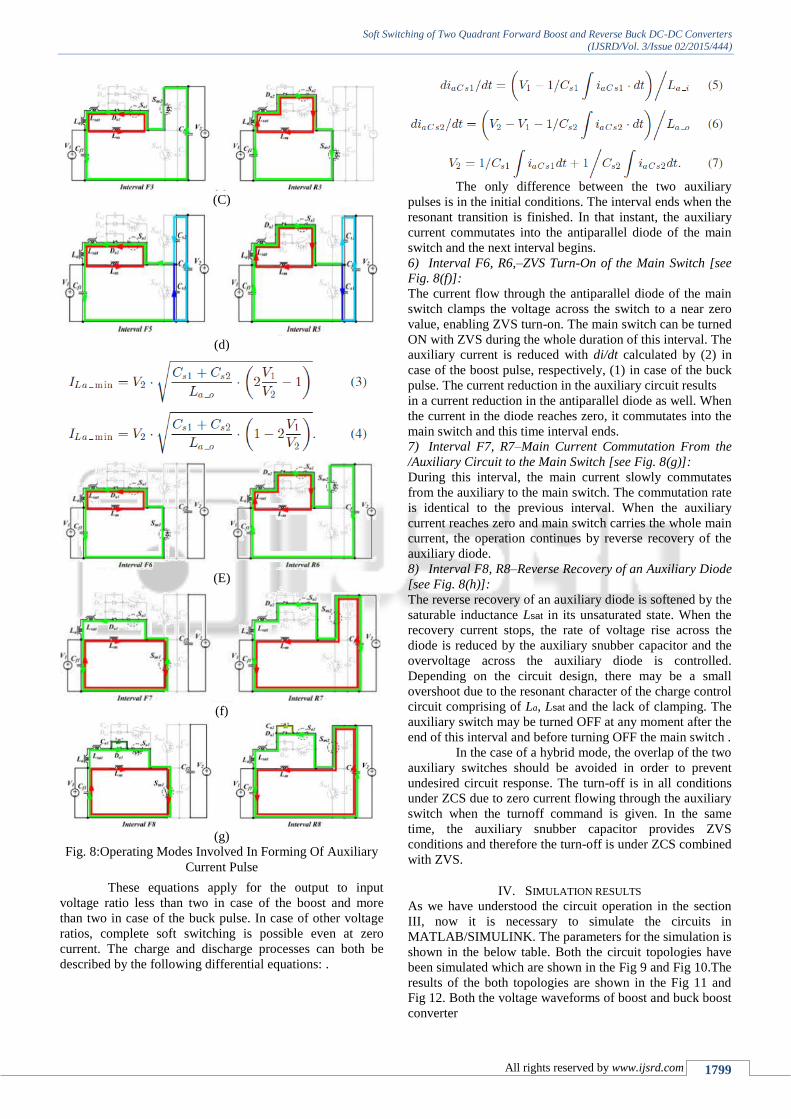
B. Boost and Buck Auxiliary Current Pulses:
1) Intervals F1, R1–Damped Discharge of the Auxiliary
Snubber Capacitor [see Fig. 8(a)]:
The starting point of this interval is the turn-on of the
auxiliary switch. Initially the auxiliary snubber capacitor
may be charged to a certain voltage level depending on the
operating point. If the capacitor is fully discharged during
intervals F10/R10 then this interval is skipped. Otherwise,
the capacitor is discharged in a resonant fashion and the
auxiliary current commutates to the auxiliary diode. The rate
of discharge is defined by the sumof the auxiliary
inductance La and saturable inductance Lsat in its unsaturated
state. The value of the snubber capacitor is in the order of a
few nF and, therefore, the discharge is fast in spite of the
large inductance (Lsat prior to saturation). At the beginning
of this interval, the current through the auxiliary circuit is
zero and, therefore, the auxiliary switch turns ON with ZCS.
As discussed previously, the auxiliary diode turns ON
essentially with ZVS in all operating points due to the
presence of the auxiliary snubber capacitor. The next
interval begins when the auxiliary diode turns ON.
2) Interval F2, R2–Main Current Commutation to
AuxiliaryCircuit [see Fig. 8(b)]:
The interval begins when the auxiliary capacitor is fully
discharged and the auxiliary current starts flowing through
the auxiliary diode. The main current ILm commutates from
the main switch to the auxiliary circuit. The saturable
inductor Lsat saturates a short while after the beginning of
the interval. The rate of the current rise during this interval
is limited by the auxiliary inductor La together with the
residual inductance of the saturable inductor. This rate is
defined by (1) in case of F2 and by (2) in case of R2
where La o is the total auxiliary inductance present in the
auxiliary path between the input capacitor Cf 1 and output
capacitor Cf 2 , and La i is the auxiliary inductance including
connections to the input filter capacitor Cf 1 . The two values
may slightly differ depending on the converter structural
layout. The auxiliary current continues to rise until the
moment it reaches the value of the main inductor current. In
the same time, the current in the main switch reaches zero
and the operation continues by the next time interval.
3) Interval F3, R3–Reverse Recovery of the Main Diode
[see Fig. 8(c)]:
At the beginning of this interval, the main current has
commutated fully to the auxiliary circuit and, therefore, the
main diode must go through its reverse recovery. The
recovery proceeds with the same di/dt as present in the
previous interval. Selection of the auxiliary inductance La
provides a degree of control over the di/dt and hence over
the reverse recovery. If SR is used and ERC is not required
for complete soft switching, the SR switch should be turned
OFF at the zero current crossing to minimise the recovery.
Once the recovery is over, the operation continues by
Interval F5, R5. If ERC is required, the SR switch remains
ON beyond the zero current crossing and the circuit
operation continues by the following time interval.
4) Interval F4, R4–Building Up Current for the Complete
ZVS Turn-Off of the Main Switch [see Fig. 8(d)]:
This interval is used if the complete soft switching cannot be
attained due to low load or small ratio between the input and
output voltage. The auxiliary current continues rising with
di/dt defined by (1), respectively, (2). SR is turned OFF
when the auxiliary current reaches the value required for
complete soft switching and the next interval begins.
5) Interval F5, R5–Resonant Main Voltage Commutation
[see Fig. 8(e)]:
At the beginning of this interval, the auxiliary current
commutates to the snubber capacitors Cs1 and Cs2 . These
can now be fully charged, respectively, discharged since the
current has a required or higher than required value. The
minimum auxiliary current required for complete resonant
voltage transition and hence complete ZVS of main switches
can be calculated by (3) for the boost pulse and by (4) for
the buck auxiliary pulse
(a)
(b)
Soft Switching of Two Quadrant Forward Boost and Reverse Buck DC-DC Converters
(IJSRD/Vol. 3/Issue 02/2015/444)
All rights reserved by www.ijsrd.com 1799
(C)
(d)
(E)
(f)
(g)
Fig. 8:Operating Modes Involved In Forming Of Auxiliary
Current Pulse
These equations apply for the output to input
voltage ratio less than two in case of the boost and more
than two in case of the buck pulse. In case of other voltage
ratios, complete soft switching is possible even at zero
current. The charge and discharge processes can both be
described by the following differential equations: .
The only difference between the two auxiliary
pulses is in the initial conditions. The interval ends when the
resonant transition is finished. In that instant, the auxiliary
current commutates into the antiparallel diode of the main
switch and the next interval begins.
6) Interval F6, R6,–ZVS Turn-On of the Main Switch [see
Fig. 8(f)]:
The current flow through the antiparallel diode of the main
switch clamps the voltage across the switch to a near zero
value, enabling ZVS turn-on. The main switch can be turned
ON with ZVS during the whole duration of this interval. The
auxiliary current is reduced with di/dt calculated by (2) in
case of the boost pulse, respectively, (1) in case of the buck
pulse. The current reduction in the auxiliary circuit results
in a current reduction in the antiparallel diode as well. When
the current in the diode reaches zero, it commutates into the
main switch and this time interval ends.
7) Interval F7, R7–Main Current Commutation From the
/Auxiliary Circuit to the Main Switch [see Fig. 8(g)]:
During this interval, the main current slowly commutates
from the auxiliary to the main switch. The commutation rate
is identical to the previous interval. When the auxiliary
current reaches zero and main switch carries the whole main
current, the operation continues by reverse recovery of the
auxiliary diode.
8) Interval F8, R8–Reverse Recovery of an Auxiliary Diode
[see Fig. 8(h)]:
The reverse recovery of an auxiliary diode is softened by the
saturable inductance Lsat in its unsaturated state. When the
recovery current stops, the rate of voltage rise across the
diode is reduced by the auxiliary snubber capacitor and the
overvoltage across the auxiliary diode is controlled.
Depending on the circuit design, there may be a small
overshoot due to the resonant character of the charge control
circuit comprising of La, Lsat and the lack of clamping. The
auxiliary switch may be turned OFF at any moment after the
end of this interval and before turning OFF the main switch .
In the case of a hybrid mode, the overlap of the two
auxiliary switches should be avoided in order to prevent
undesired circuit response. The turn-off is in all conditions
under ZCS due to zero current flowing through the auxiliary
switch when the turnoff command is given. In the same
time, the auxiliary snubber capacitor provides ZVS
conditions and therefore the turn-off is under ZCS combined
with ZVS.
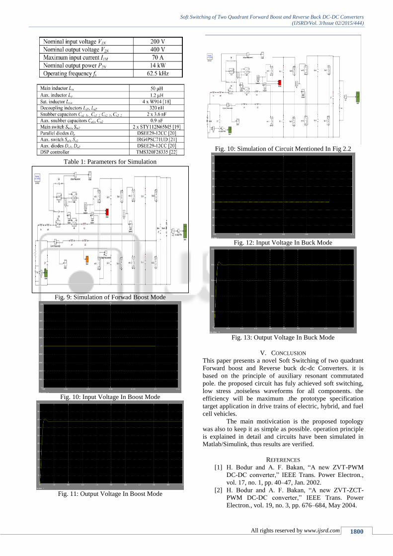
IV. SIMULATION RESULTS
As we have understood the circuit operation in the section
III, now it is necessary to simulate the circuits in
MATLAB/SIMULINK. The parameters for the simulation is
shown in the below table. Both the circuit topologies have
been simulated which are shown in the Fig 9 and Fig 10.The
results of the both topologies are shown in the Fig 11 and
Fig 12. Both the voltage waveforms of boost and buck boost
converter
Soft Switching of Two Quadrant Forward Boost and Reverse Buck DC-DC Converters
(IJSRD/Vol. 3/Issue 02/2015/444)
All rights reserved by www.ijsrd.com 1800
Table 1: Parameters for Simulation
Fig. 9: Simulation of Forwad Boost Mode
Fig. 10: Input Voltage In Boost Mode
Fig. 11: Output Voltage In Boost Mode
Fig. 10: Simulation of Circuit Mentioned In Fig 2.2
Fig. 12: Input Voltage In Buck Mode
Fig. 13: Output Voltage In Buck Mode
V. CONCLUSION
This paper presents a novel Soft Switching of two quadrant
Forward boost and Reverse buck dc-dc Converters. it is
based on the principle of auxiliary resonant commutated
pole. the proposed circuit has fuly achieved soft switching,
low stress ,noiseless waveforms for all components. the
efficiency will be maximum .the prototype specification
target application in drive trains of electric, hybrid, and fuel
cell vehicles.
The main motivication is the proposed topology
was also to keep it as simple as possible. operation principle
is explained in detail and circuits have been simulated in
Matlab/Simulink, thus results are verified.
REFERENCES
[1] H. Bodur and A. F. Bakan, “A new ZVT-PWM
DC-DC converter,” IEEE Trans. Power Electron.,
vol. 17, no. 1, pp. 40–47, Jan. 2002.
[2] H. Bodur and A. F. Bakan, “A new ZVT-ZCT-
PWM DC-DC converter,” IEEE Trans. Power
Electron., vol. 19, no. 3, pp. 676–684, May 2004.

Soft Switching of Two Quadrant Forward Boost and Reverse Buck DC-DC Converters
(IJSRD/Vol. 3/Issue 02/2015/444)
All rights reserved by www.ijsrd.com 1801
[3] M. Pavlovsky, Y. Tsuruta, and A. Kawamura, “Bi-
directional buck/boost dc-dc converter with ultra
high efficiency based on improved SAZZ
topology,” in Proc. Energy Convers. Cong.
Exposition, ECCE 2009, pp. 1783-1790.
[4] S. Chattopadhyay, S. Baratam, and H. Agrawal, “A
new family of active clamp PWM dc-dc converters
with ZVS for main switch and ZCS for auxiliary
switch,” in Proc. Applied Power Electron. Conf.
Exposition, APEC 2011, pp. 851–858.
[5] A. Elasser and D. A. Torrey, “Soft switching active
snubbers for DC/DC converters,” IEEE Trans.
Power Electron., vol. 11, no. 5, pp. 710–722, Sep.
1996.
[6] I. Aksoy, H. Bodur, and A. F. Bakan, “A New
ZVT-ZCT-PWM DC–DC Converter,” IEEE Trans.
Power Electron., vol. 25, no. 8, pp. 2093–2105,
Aug. 2010.
[7] B. Ivanovic and Z. Stojiljkovic, “A novel active
soft switching snubber designed for boost
converter,” IEEE Trans. Power Electron., vol. 19,
no. 3, pp. 658–665, May 2004.
[8] K-J. Lee, B.-G. Park, R-Y. Kim, and D-S. Hyun,
“Nonisolated ZVT twoinductor boost converter
with a single resonant inductor for high step-up
applications,” IEEE Trans. Power Electron., vol.
27, no. 4, pp. 1966–1973, Apr. 2012.
[9] T.-F. Wu, Y.-D. Chang, C.-H. Chang, and J.-G.
Yang, “Soft-switching boost converter with a
flyback snubber for high power applications,”
IEEE Trans. Power Electron., vol. 27, no. 3, pp.
1108–1119, Mar. 2012.
Recommended