University of South FloridaScholar Commons
Graduate Theses and Dissertations Graduate School
October 2017
Smart Inverter Control and Operation forDistributed Energy ResourcesAhmad F. TazayUniversity of South Florida, [email protected]
Follow this and additional works at: http://scholarcommons.usf.edu/etd
Part of the Electrical and Computer Engineering Commons
This Dissertation is brought to you for free and open access by the Graduate School at Scholar Commons. It has been accepted for inclusion inGraduate Theses and Dissertations by an authorized administrator of Scholar Commons. For more information, please [email protected].
Scholar Commons CitationTazay, Ahmad F., "Smart Inverter Control and Operation for Distributed Energy Resources" (2017). Graduate Theses and Dissertations.http://scholarcommons.usf.edu/etd/7097

Smart Inverter Control and Operation for Distributed Energy Resources
by
Ahmad F. Tazay
A dissertation submitted in partial fulfillmentof the requirements for the degree of
Doctor of PhilosophyDepartment of Electrical Engineering
College of EngineeringUniversity of South Florida
Major Professor: Zhixin Miao, Ph.D.Lingling Fan, Ph.D.
Chung Seop Jeong, Ph.D.Kaiqi Xiong, Ph.D.Zhenyu Wang, Ph.D.
Date of Approval:October 20, 2017
Keywords: Microgrid, Voltage Source Converter (VSC), Three-phase Hybrid Boost Converter(HBC), Droop Control, PV Charging Station
Copyright c 2017, Ahmad F. Tazay

DEDICATION
I dedicate my dissertation work to my amazing parents, Fareed and Ghofran, for being the
perfect parent role model, for their inspiration, continuous prayers, and belief in me. To my dear
wife, Omniah, for being a perfect wife, the love of my life, being always optimistic, tolerating my
excessive work and study times, and her unconditional love. I hope that you receive your degree
soon. To my wonderful parents in law, Amin and Meme, for being cheerful and positive towards
every decision I made. To my beautiful kids, Rawad and Rozana, for always making me smile and
happy. You are my luminous future. To my lovely brothers and sister, Emad, Nader, Nezar, and
Rasha, for their love, support, and understanding my situation.I love you all. You are the secret
behind my success.

ACKNOWLEDGMENTS
I would like to express my deepest gratitude to my major advisor Dr. Zhixin Miao for sup-
porting, encouraging, guidance, technical insight, and providing me with an excellent atmosphere
to do research throughout the past four years. His incredible hard-working, trust in my abilities,
and deep work reviews had a serious influence on my motivation and professional growth.
I would also like to thank Dr. Lingling Fan for providing me the necessary tools which were
required to develop my research. I especially appreciate her great knowledge and experience, hard-
working, patience, and great kindness and morality.
I would like to truly thank my committee members: Dr. Chung Seop Jeong, Dr. Kaiqi Xiong,
and Dr. Zhenyu Wang, for their encouragement, constructive comments, reviewing my dissertation
and participating in my dissertation.
I would also like to thank my recent colleagues from the smart grid power system lab Yan Ma,
Yin Li, David Xu, Matthew Ma, Yi Zhou, Anas Almunif, Ibrahim Alsaleh, Abdullah Alburidy,
Rabi Kar, Miao Zhang, Li Bao, Sulaiman Almutairi, Abdullah Alassaf, Tony Wang, and my former
colleagues Dr. Mohemmed Alhaider, Dr. Hossein Aghamolki, Dr. Vahid Rasouli, Dr. Lakshan
Piyasinghe, Dr. Javad Khazaei, for all the discussions, help and enjoyable time I spent with them.
Special thanks go to my missing friend, Ayman Aldhmadi, who passed away before joining our lab.
May Allah forgive him and his soul rest in peace.
I would also like to o↵er sincere thanks and gratitude to my family. I would like to thank my
wife, Omniah Baghdady, my father, Fareed Tazay, my mother, Ghofran Mosatat, my father in law,
Amin Baghdady, my mother in law, Meme Ghandorah,my brothers, Emad, Nader and Nezar, my
sister, Rasha for all the encouragement, love and the support they provided from the beginning. I
am truly grateful for their love and support.

TABLE OF CONTENTS
LIST OF TABLES iv
LIST OF FIGURES v
ABSTRACT viii
CHAPTER 1 INTRODUCTION 11.1 Background 1
1.1.1 Microgrid 21.1.2 Energy Resources 3
1.1.2.1 Photovoltaic (PV) 31.1.2.2 Battery 41.1.2.3 Plug-In Hybrid Electric Vehicle (PHEV) 5
1.1.3 Smart Inverter 61.2 Research Significance 91.3 Statement of the Problem 11
1.3.1 Induction Motor Load at Autonomous Microgrid 111.3.1.1 Blackstart 111.3.1.2 Common Mode Voltage 12
1.3.2 PV Charging Station 121.3.3 Circulating Current 13
1.4 Approach 131.4.1 VSC Control for Motor Drive 14
1.4.1.1 Vector Control Based Soft Start 141.4.1.2 Switching Scheme 14
1.4.2 Hybrid Smart Converter Topology 151.4.3 Centralized Control of Smart Inverters 16
1.5 Outline of the Dissertation 16
CHAPTER 2 CONTROL OF SMART INVERTER AND VSC 182.1 General Overview 182.2 Microgrid Configuration 20
2.2.1 Pulse Width Modulator (PWM) 212.2.2 RLC Filter 222.2.3 Dc-Link Capacitor 22
2.3 Smart Inverter Control 232.3.1 Smart Inverter at Grid-Connected Mode 25
i

2.3.1.1 Vector Transformation Concept 252.3.1.2 Phase Locked Loop (PLL) 282.3.1.3 PLL Controller Design 302.3.1.4 PQ Plant Model 302.3.1.5 PQ Controller Design 36
2.3.2 Smart Inverter at Autonomous Mode 402.3.2.1 VF Plant Model 412.3.2.2 VF Controller Design 44
CHAPTER 3 SMART INVERTER CONTROL FOR MOTOR DRIVES 483.1 Review of Motor Drives 48
3.1.1 Blackstart Phenomena 483.1.2 Common Mode Voltage (CMV) Concept 49
3.2 Smart Inverter Topology 503.3 Controlling Challenges of Induction Motor 51
3.3.1 Induction Motor’s Blackstart 513.3.2 Induction Motor’s Switching Scheme 52
3.4 Proposed Methods for Motor Drive 533.4.1 Soft Start 533.4.2 Active Zero Pulse Width Modulation (AZPWM) 54
3.5 Simulation Results 573.5.1 Soft Start Algorithm for Blackstart Issue 573.5.2 AZPWM Algorithm for CMV Issue 59
CHAPTER 4 CONTROL OF HYBRID CONVERTER FOR PV STATION 624.1 Introduction 624.2 Three-Phase HBC-based PV Charging Station 65
4.2.1 Shoot-Through Phase (ST) 684.2.2 Active Phase (A) 684.2.3 Zero Phase (Z) 684.2.4 Modified PWM 704.2.5 Modeling of PV Array 72
4.3 Control of PV Charging Station 734.3.1 Maximum Power Point Tracking (MPPT) 734.3.2 Synchronous Rotating Reference Frame PLL (SRF-PLL) 764.3.3 Vector Control for PV Charging Station 764.3.4 O↵-board Battery Charger 79
4.4 Power Management and Operation Modes 844.4.1 Mode I: PV Powers PHEV and the Utility 844.4.2 Mode II: PV and the Utility Power the PHEV 854.4.3 Mode III: The Utility only Powers the PHEV 85
4.5 Simulation Results 854.5.1 Case 1: Performance of Modified IC-MPPT 874.5.2 Case 2: Performance of the DC Voltage Controller 894.5.3 Case 3: Reactive Power and Grid Fault 904.5.4 Case 4: Power Management of the PV Charging Station 92
ii

4.5.5 Performance of O↵-board dc/dc Converter 93
CHAPTER 5 COORDINATION OF SMART INVERTERS 955.1 Introduction 955.2 Analysis and Modeling of an Autonomous Microgrid 97
5.2.1 System Configuration 975.2.2 Control of Smart Inverter Using Primary Droop Control 995.2.3 Reactive Power Sharing 1025.2.4 Circulating Current Analysis 105
5.3 Proposed Secondary Control 1075.3.1 Concept and Topology 1075.3.2 Controlling Strategy 109
5.4 Simulation Results 1115.4.1 Case1: SCUM Operation 1125.4.2 Case2: SCUM Operation Under Ocillator System 114
5.5 Conclusion 116
CHAPTER 6 CONCLUSIONS AND FUTURE WORK 1176.1 Conclusion 1176.2 Future Work 118
REFERENCES 119
APPENDICES 130Appendix A Reuse Permissions of Published Papers for Chapters 2 and 3 131Appendix B List of Abbreviations and Symbols 133
ABOUT THE AUTHOR End Page
iii

LIST OF TABLES
Table 1.1 Comparison between the functions of smart inverter and VSC 9
Table 2.1 Controller’s parameters for the inner current loop 38
Table 2.2 Controller’s parameters for the outer power loop 39
Table 2.3 Controller’s parameters for the outer voltage loop 46
Table 3.1 Switching sequences for SVPWM and AZPWM1 at di↵erent sectors 57
Table 3.2 Parameters of an autonomous microgrid to operated the motor drives 57
Table 3.3 Di↵erent cases of voltage ramp to operate a smart inverter 59
Table 4.1 System parameters of a PV charging station 87
Table 5.1 System parameters of three DER units forming autonomous microgrid 111
Table 5.2 Control parameters of primary and secondary controllers 112
iv

LIST OF FIGURES
Figure 1.1 Configuration of a three-phase bidirectional VSC converter 2
Figure 1.2 Overall view of a multifunction smart inverter 8
Figure 2.1 Single-line configuration of a microgrid using vector controller 20
Figure 2.2 DQ and ↵ reference frames 27
Figure 2.3 Basic schematic diagram of an SRF-PLL 29
Figure 2.4 Linearized model of SRF-PLL 29
Figure 2.5 Bode plot of open-loop transfer function of SRF-PLL 31
Figure 2.6 Bode plot of closed-loop transfer function of SRF-PLL 32
Figure 2.7 Phase circuit diagram of a smart inverter at grid-connected mode 33
Figure 2.8 Simplified control block diagram of the inner current loop 34
Figure 2.9 Block diagram of real and reactive power controllers 35
Figure 2.10 Bode plot of the open-loop transfer function of inner current controller 39
Figure 2.11 Bode plot of the closed-loop transfer function of inner current controller 40
Figure 2.12 Bode plot of the open-loop transfer function of outer power controller 41
Figure 2.13 Bode plot of the closed-loop transfer function of outer power controller 42
Figure 2.14 Phase circuit diagram of a smart inverter based grid-connected mode 43
Figure 2.15 Block diagram of voltage controllers 45
Figure 2.16 Bode plot of the open-loop of outer voltage controller 47
Figure 2.17 Bode plot of the closed-loop of outer voltage controller 47
Figure 3.1 General controller scheme and topology of motor drives 50
Figure 3.2 SVPWM and AZPWM representation at ↵ reference frame 53
v

Figure 3.3 Starting current and reactive power characteristic using DOL method 54
Figure 3.4 Current and reactive power relation with stator voltage at soft start 55
Figure 3.5 Switching sequence based on 7-segment method at sector one 56
Figure 3.6 Microgrid behavior using DOL method 58
Figure 3.7 Microgrid behavior using soft start method 59
Figure 3.8 Output voltage of the microgrid using VF controller 60
Figure 3.9 SVPWM method to operate smart inverter at autonomous microgrid 61
Figure 3.10 AZPWM method to operate smart inverter at autonomous microgrid 61
Figure 4.1 Architecture configuration of a PV charging station 65
Figure 4.2 Detailed model of PV charging station 66
Figure 4.3 The three operational intervals of the three-phase HBC 67
Figure 4.4 Behavior of the HBC’s components during operational periods 69
Figure 4.5 Modified PWM for the three-phase-HBC 71
Figure 4.6 Two diode model of PV 72
Figure 4.7 Control blocks of the HBC-based PV charging station. 73
Figure 4.8 IV-curve for Sunpower SPR-E20-327 74
Figure 4.9 MPPT technique for PV using modified IC-MPPT method 76
Figure 4.10 Vector control scheme of the three-phase HBC 77
Figure 4.11 Bode plot for open loop current controller 80
Figure 4.12 Bode plot for open loop voltage controller 80
Figure 4.13 Bode plot for closed loop controller 81
Figure 4.14 A simple diagram of CC-CV technique for PHEV’s battery charging 82
Figure 4.15 O↵-board charging structure using CC-CV algorithm 83
Figure 4.16 Operation modes of PV’s charging station 86
Figure 4.17 Performance of a modified IC-PI MPPT algorithm 88
Figure 4.18 Performance of the dc voltage control in the vector control 89
vi

Figure 4.19 Performance of a proposed vector control using reactive power 90
Figure 4.20 System performance under 50% grid’s voltage drop 91
Figure 4.21 Power management of PV charging station 92
Figure 4.22 Performance of CC-CV algorithm 93
Figure 4.23 Dst
, Md
and Mq
for case 4 94
Figure 4.24 The modified PWM signals and the switching sequences 94
Figure 5.1 Single line-configuration of a microgrid 98
Figure 5.2 Block diagram of the autonomous microgrid 99
Figure 5.3 Simplified two-DER units microgrid with mismatched line impedance 103
Figure 5.4 Detailed primary and secondary controllers for autonomous microgrid 108
Figure 5.5 Block diagram of reactive power control 110
Figure 5.6 Simulation results for case 1 at stable system 113
Figure 5.7 Simulation results for case 2 at high oscillated system 115
vii

ABSTRACT
The motivation of this research is to carry out the control and operation of smart inverters
and voltage source converters (VSC) for distributed energy resources (DERs) such as photovoltaic
(PV), battery, and plug-in hybrid electric vehicles (PHEV). The main contribution of the research
includes solving a couple of issues for smart grids by controlling and implementing multifunctions
of VSC and smart inverter as well as improving the operational scheme of the microgrid. The work
is mainly focused on controlling and operating of smart inverter since it promises a new technology
for the future microgrid. Two major applications of smart inverter will be investigated in this work
based on the connection modes: microgrid at grid-tied mode and autonomous mode.
In grid-tied connection, the smart inverter and VSC are used to integrate DER such as Pho-
tovoltaic (PV) and battery to provide suitable power to the system by controlling the supplied
real and reactive power. The role of a smart inverter at autonomous mode includes supplying a
sucient voltage and frequency, mitigate abnormal condition of the load as well as equally sharing
the total load’s power. However, the operational control of the microgrid still has a major issue on
the operation of the microgrid. The dissertation is divided into two main sections which are:
• 1- Low-level control of a single smart Inverter.
• 2- High-level control of the microgrid.
The first part investigates a comprehensive research for a smart inverter and VSC technology at the
two major connections of the microgrid. This involves controlling and modeling single smart inverter
and VSC to solve specific issues of microgrid as well as improve the operation of the system. The
research provides developed features for the smart inverter comparing with a conventional voltage
sourced converter (VSC). The two main connections for a microgrid have been deeply investigated
to analyze a better way to develop and improve the operational procedure of the microgrid as well
as solve specific issues of connecting the microgrid to the system.
viii

A detailed procedure for controlling VSC and designing an optimal operation of the controller
is also covered in the first part of the dissertation. This section provides an optimal operation
for controlling motor drive and demonstrates issues when motor load exists at an autonomous
microgrid. It also provides a solution for specific issues at operating a microgrid at autonomous
mode as well as improving the structural design for the grid-tied microgrid. The solution for
autonomous microgrid includes changing the operational state of the switching pattern of the
smart inverter to solve the issue of a common mode voltage (CMV) that appears across the motor
load. It also solves the issue of power supplying to large loads, such as induction motors. The last
section of the low-level section involves an improvement of the performance and operation of the
PV charging station for a plug-in hybrid electric vehicle (PHEV) at grid-tied mode. This section
provides a novel structure and smart controller for PV charging station using three-phase hybrid
boost converter topology. It also provides a form of applications of a multifunction smart inverter
using PV charging station.
The second part of the research is focusing on improving the performance of the microgrid by
integrating several smart inverters to form a microgrid. It investigates the issue of connecting DER
units with the microgrid at real applications. One of the common issues of the microgrid is the
circulating current which is caused by poor reactive power sharing accuracy. When more than two
DER units are connected in parallel, a microgrid is forming be generating required power for the
load. When the microgrid is operated at autonomous mode, all DER units participate in generating
voltage and frequency as well as share the load’s power. This section provides a smart and novel
controlling technique to solve the issue of unequal power sharing. The feature of the smart inverter
is realized by the communication link between smart inverters and the main operator. The analysis
and derivation of the problem are presented in this section.
The dissertation has led to two accepted conference papers, one accepted transaction IEEE
manuscript, and one submitted IET transaction manuscript. The future work aims to improve the
current work by investigating the performance of the smart inverter at real applications.
ix

CHAPTER 1
INTRODUCTION
This chapter introduces the advantages of a smart inverter and microgrid technology as well as
presents the main objectives of this research.
1.1 Background
Power electronics play an important role in operating and controlling the microgrid. Voltage
sourced converter (VSC) is one of the commonly used power electronic devices that are recently
implemented in a microgrid instead of conventional electronic devices such as thyristor-based line-
commutated converters (LCC). The development in power electronics industry leads to increase
the power capacity and response speed of Insulated-Gate Bipolar Transistors (IGBTs). The main
benefits of using VSC instead of LCC is the implementing of IGBT components to control of
switching patterns. Moreover, The IGBT based VSC is controlled by gate voltage which does
not require an external circuit to turn o↵ the device. Another advantage is the bidirectional
power flow capability of VSC. The topology of VSC can be operated as dc/ac inverter and ac/dc
converter based on the advanced configuration of the VSC. These advantages lead to implement
VSC in several applications such as PV microgrid, high-voltage direct current (HVDC), flexible ac
transmission systems (FACTS), Static Compensator (STATCOM), plug-in hybrid vehicle charging
stations (PHEV), etc.
There are several topologies to represent IGBT based VSC device regarding the required power
capacity of the module. For example, two-level PWM converter and three-level neutral-point clamp
converter are the common topologies of VSC based on cost and eciency aspects. It is worth to
mention that IGBT has the capability to be connected in series to form a modular multilevel
converter (MMC) which can be used at high-voltage applicants such as HVDC systems. In this
1

dissertation, the two-level three-phase bidirectional IGBT switches are implemented to represent a
VSC converter. Fig. 1.1 shows a common topology of a three-phase tow-level IGBT based VSC
converter. It is noticed from designing of IGBT switches that every VSC’s switch has a reverse
parallel diode. The key role of the diode is to achieve a bidirectional current flow without a↵ecting
the power rating of each VSC leg. This configuration allows VSC to be operated as a dc/ac inverter
or an ac/dc converter without any topology change.
S1
S4
S3
S2
S5
S6
ia
ib
icVdc
+
-
Figure 1.1. Configuration of a three-phase bidirectional VSC converter
1.1.1 Microgrid
The advanced feature and recent development of power electronic filed have convinced the elec-
tric industry to depend on distributed energy resources (DERs) to generate electric power on smart
grid and microgrid. The leading action of integrating smart grid and microgrid into the main grid
can solve most of the system’s problems as well as improve the eciency and reliability. The fu-
ture of power systems will depend on generating electricity from the microgrid since it can supply
sucient power to its local load as well as share energy with the entire system.
Microgrid is a distributed network that provides controllable power and energy to the entire
system by integrating DERs with the system and loads using power electronics technologies. These
2

main elements are electronically interfaced to provide controllable power, stable voltage, and steady
frequency to the entire system. DER consists of Distributed Storages (DS) or a Distributed Gen-
erators (DG). Loads may include a combination of resistive, inductive and capacitive elements as
well as distributed power storage equipment or motors. Generally, DG contains non-conventional
and clean energy resources such as wind, solar photovoltaic, fuel-cell, etc.
The future technology of a microgrid promises to adopt more distributed generation and con-
sumption to represent a whole unit in one system. This development requires the participation
of consumer to generate and manage energy as well as store the extra energy to support neigh-
bor microgrids. The common condition of a microgrid is a grid-connected mode where the DG
is connected to the main distributed network to supply energy and support the main elements of
the power system. The supplied power of DG can be controlled at grid-connected mode where the
voltage and frequency are supported by the main grid. In some cases such as disturbance and fault
in the grid or limitation of providing power from the main grid to an autonomous area, the DG
is responsible for providing a stable voltage and frequency to the load. This condition is called
autonomous mode and it is usually applied in an autonomous area.
1.1.2 Energy Resources
This section provides common energy resources that are used in the research. It is recommended
to notice that there are other energy resources that will be covered in the future work such as fuel-
cell and wind energy.
1.1.2.1 Photovoltaic (PV)
Photovoltaic (PV) is a renewable energy resource that converts the solar energy (photons) into
dc electric energy (voltage) using the variety of materials such as silicon or cadmium telluride [1].
PV array consists of series and parallels connected modules and each module includes the variety of
series cells. Generally, the PV system is connected to power electronic devices to extract maximum
power and converter the generated dc power into ac power. VSC is applied in PV system to
converter dc power into ac power while dc/dc converter is used to achieve maximum power point
3

tracking (MPPT) control. MPPT aims to tracks the maximum generated power from the PV even
at changing weather or load disturbance.
There are several methods to apply MPPT on dc/dc converter or VSC. For example, incremental
conductance (IC), perturb and observe (PO), hill climbing (HC), fuzzy logic control, and fractional
control [2, 3]. Several studies have been investigated the advantages and disadvantages of each
MPPT algorithm in order to improve the performance of MPPT. The paper in [4] claims that
PO method provides error around the maximum power point. Adaptive HC is proposed in [5] to
overcome the issues of PO. Even PO and HC can provide simple implementation, they su↵er from
steady state and dynamic stability issues. IC algorithm has an advantage of providing slow tracking
of maximum power which o↵ers high eciency compared with other MPPT methods [6]. Several
manuscripts aim to improve the performance of IC method such as variable step size method [7], IC
slop change [8], and dead-band based IC algorithm [9]. In this dissertation, improved IC algorithm
is applied to control of MPPT of PV array.
Distributed energy resources such as PV gains more interesting in research and industry fields.
Installation of PV has been growing recently due to reliability, power quality, and low maintenance.
In recent years, the penetration of PV into the smart grid has been significantly increased due to
reducing operational cost and high eciency. Considering the advantages of PV, it is forecasted
that the PV microgrid will be the dominated renewable energy source in 2040 [3, 10, 11].
However, the increment penetration of PV may generate steady state and transient issues to
the gird. Moreover, PV array supplies a dc power source while most of the loads and the main grid
need to receive high-quality ac power. So, the need of converting dc power to ac power is essential
to meet the load’s requirements in microgrids [12].
1.1.2.2 Battery
Distributed energy resources (DERs) such as PV system requires energy storage elements in
order to achieve stability and increase reliability. Since the operation period of the PV array is dur-
ing the daytime, implementing energy storage such as a battery is important to achieve continuous
power supply to the load or main grid. Energy storage application can provide several advantages
4

to the microgrid based on stability, eciency, and reliability aspects. One of the advantages of
the energy storage is that it can mitigate the limitation of DER. For example, battery storage can
provide a sucient power to the local load at night where the PV array cannot generate any power
during weather condition such as cloud shadow and absence of sunlight [13].
Battery storage can be controlled using VSC based on the operating condition of the microgrid.
Generally, the microgrid can be operated at two operational conditions which are grid-connected
mode and autonomous mode. At grid-connected modes, the power electronics of battery systems
will work at PQ control by providing stored power to the main grid. The battery may operate at
charging or discharging condition based on the state of charge (SOC) of the battery. The applica-
tion of the battery at grid-connected mode is presented in [14–16].
The autonomous mode of the microgrid requires a dicult control since it has to support the
required voltage and frequency of the local loads as well as sharing the total load power. PV system
alone could not be operated at autonomous condition regarding the weather condition and power
limitation of the system. As a solution, battery storage has to be applied to support the voltage
and frequency of the supplied PV array. VSC is used to control the voltage and frequency of the
battery as well as regulate the charging and discharging procedures. The PV battery system is
presented in several manuscripts such as [17–19].
Since the battery storage is important to operate the microgrid, modeling and controlling of
the battery is needed. It is also required to analyze the battery limitation in order to achieve
real implementation. For example, the SOC cannot be lower than a threshold and the depth of
discharge (DOD) may impact the lifetime of the battery. Most of battery storage systems adopt
the Li-ion battery because its high eciency [20]. The di↵erential equations modeling of Li-ion
battery is presented in [21]. A detailed battery model of Li-ion is described in [22]. Dynamic model
and experimental approach of the battery are shown in [23].
1.1.2.3 Plug-In Hybrid Electric Vehicle (PHEV)
The environmental and economic advantages of plug-in hybrid vehicle PHEV lead to the in-
crease in a number of production and consumption. The U.S. Department of Energy forecasts that
5

over one million PHEVs will be sold in the U.S. during the next decade [24]. PHEV is operated
at two power sources which are battery and internal combustion engine using fossils fuel energy.
This feature increases the liability of the vehicle and reduces the operational cost. So, it has the
advantage of long driving range since gas fuel is considered as a secondary consumption resource.
The PHEV’s battery can be charged using ac or dc outlet. Di↵erent charging levels are provided
based on the charging speed and time [25].
Power electronics play an important role in controlling the charging of PHEV’s battery. The
battery chargers are classified as on-board and o↵-board converters with unidirectional or bidirec-
tional power feature [26]. The benefit of PHEV’s battery is not only reducing the dependency on
conventional fossils fuel, but it can support the power quality by injecting energy back to the grid
using the vehicle to grid feature. Modeling and controlling of a PV system interfaced with PHEV
battery is a hot topic. In [27], modeling and power management of PV charging station is driven.
The control strategy of battery and PV using VSC is presented in [28]. Hybrid microgrid to control
of PV integrated PHEV is proposed in [29].
1.1.3 Smart Inverter
The recent improvements toward smart building and smart grids forced the power electronic
industry to raise the industry’s standards and regulation for designing and operating power elec-
tronics based on several issues such as:
• Power flow direction.
• Voltage flicker.
• Harmonic distortion.
• System reliability.
• Protection issues.
• Frequency stability.
• Voltage stability.
6

Conventional VSC could not solve these aforesaid issues and the need for defining smarter features
for PV inverters are essential. Furthermore, the increasing need for satisfying the load demand and
changing reliance on conventional power source support the necessity for smart features of VSC.
Unidirectional power flow is no longer be e↵ective for controlling microgrids. Decentralized
power system where bidirectional power flows between the DER and the main grid, provides an
additional issue to the system. Changing power flow may cause voltage rise conditions at steady
state as well as an unstable problem at the point of common coupling (PCC) due to overproduction
of PV energy. In transient condition, the interconnection of PV system might lead to voltage flicker,
harmonic distortion, system reliability problem and protection issues. [12].
Other observed problem of PV microgrid is that solar panels might generate frequent voltage
flicker due to shadow clouds or suddenly disconnected from the grid. In addition, tripping or
overproduction of PV feeders may cause frequency stability issues [30]. Even though centralized
control and communication resources can mitigate the impact of frequency and voltage fluctuation,
operational control of DG still dicult in modern decentralized energy systems. So, conventional
inverters could not solve these issues and the need for defining smarter features for PV inverters is
essential. Furthermore, the aforementioned issues and the increasing need for satisfying the load
demand support the necessity for a smart inverter.
In order to improve the stability and reliability of the microgrid as well as solve the challenges
of operating microgrids, several companies and research groups have issued standards and proto-
cols for operating VSC based microgrid. The Electric power research institute (EPRI) has defined
several functions and specifications that VSC need to adopt in order to be defined as smart in-
verter [31]. California public utilities commission created the smart inverter working group (SIWG)
to issue standards for advanced inverter technologies [32]. The Society of Automotive Engineers
(SAE) has also issued recommendations for operating and controlling electrical vehicles based on
charging procedures and stability aspects [33].
Smart inverter is defined as an inverter that has the bidirectional communications capability,
send and receive operational commands, and change the current sittings. The concept of smart
inverter consists of three main components which are hardware architecture, main operator, and
7

communication network. The smart inverter operation is realized via two-way communication net-
work to send and receive information between smart inverter and the main operator. The inverter
needs first to monitor its real-data situation and send these data to the central controller. The
central controller then collect these data and submit a command signal to each inverter to change
the current operation point of the system. The command signal is transmitted based on predefined
multifunction in the main operator. These functions are defined based on the need to the load and
the main grid. These functions are capable to operate at centralized and decentralized systems as
well as any microgrid connection modes. Fig. 1.2 shows multifunction features of smart inverter.
The smart features of VSC in Fig. 1.2 can reduce the system topology as well as coordinate mul-
tiple DERs in single microgrid. It is worth to mention that the function of smart inverter is only
realized via two-way communication bus between the inverters and the main operator.
dc/dcconverter
ac/dcinverter
dc/dcconverter
Three-phase two-level
dc/ac inverter
DC Bus PCC
Smart Grid
MPPT
MultifunctionSmart Inverter
A
B
C
Solar Array
Wind Turbines
EV
MPPT
Charging Station
Energy Storage Loads
Figure 1.2. Overall view of a multifunction smart inverter
The role of smart inverters surpasses the basic functions of conventional inverters, such as max-
imum power point tracking, islanding detection, and power conversion. They can actually support
8
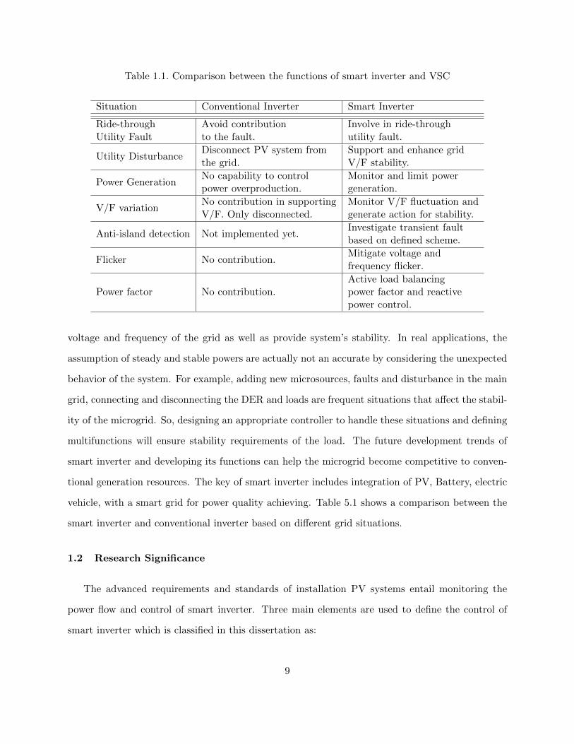
Table 1.1. Comparison between the functions of smart inverter and VSC
Situation Conventional Inverter Smart Inverter
Ride-throughUtility Fault
Avoid contributionto the fault.
Involve in ride-throughutility fault.
Utility DisturbanceDisconnect PV system fromthe grid.
Support and enhance gridV/F stability.
Power GenerationNo capability to controlpower overproduction.
Monitor and limit powergeneration.
V/F variationNo contribution in supportingV/F. Only disconnected.
Monitor V/F fluctuation andgenerate action for stability.
Anti-island detection Not implemented yet.Investigate transient faultbased on defined scheme.
Flicker No contribution.Mitigate voltage andfrequency flicker.
Power factor No contribution.Active load balancingpower factor and reactivepower control.
voltage and frequency of the grid as well as provide system’s stability. In real applications, the
assumption of steady and stable powers are actually not an accurate by considering the unexpected
behavior of the system. For example, adding new microsources, faults and disturbance in the main
grid, connecting and disconnecting the DER and loads are frequent situations that a↵ect the stabil-
ity of the microgrid. So, designing an appropriate controller to handle these situations and defining
multifunctions will ensure stability requirements of the load. The future development trends of
smart inverter and developing its functions can help the microgrid become competitive to conven-
tional generation resources. The key of smart inverter includes integration of PV, Battery, electric
vehicle, with a smart grid for power quality achieving. Table 5.1 shows a comparison between the
smart inverter and conventional inverter based on di↵erent grid situations.
1.2 Research Significance
The advanced requirements and standards of installation PV systems entail monitoring the
power flow and control of smart inverter. Three main elements are used to define the control of
smart inverter which is classified in this dissertation as:
9

• Vector Control.
• Switching Scheme.
• Schematic design.
Each part of these features needs further investigation in order to satisfy the definition of a smart
inverter. The vector control is the key element of monitoring the operational and design features
of the smart inverter. This part is the core of controlling the smart inverter since it provides the
type of supplying element based on the microgrid’s need as well as extends more stability and
quality to the system. Switching scheme of the smart inverter includes applying several methods
to change the switching patterns without a↵ecting the system’s quality and reliability. Comparing
with other controlling method, vector control has been recently applied in most of industrial appli-
cations because of the designing advantages and methodology. By changing the switching patterns
of the smart inverter, it can solve several issues of the microgrid such as harmonic distortions,
common mode voltage, and voltage drop stress. A schematic design feature of the smart inverter
is an advanced connection technique for extending the flexibility of the power sharing between the
microgrid and the main grid. The new feature of designing smart inverter can generate both dc
and ac power as well as supporting the stability of the system.
The future research on PV inverter aims to apply multifunctional smart inverter to control
and monitor the system. Smart inverter functions have to fulfill the system requirements which
involve connect/disconnect from the grid, power adjustment, charging/discharging storage man-
agement, voltage and frequency ride-through, voltage and frequency management, and islanding
detection [34]. The future research on smart grid technology also relies on renewable energy to
generate stable frequency and voltage instead of conventional energy source. This technique re-
quires achieving ancillary services such as voltage and frequency regulation, balancing power, and
blackstart. The big challenging is to practically apply the theoretical concept of conventional power
sources to be operated by renewable energy. It is also required to apply the concept of smart in-
verter to solve the issue of connected several DER units to form the microgrid. By applying smart
inverter technique, the aforementioned obstacles can be solved.
10

1.3 Statement of the Problem
The rapid development of power electronics enables a microgrid to participate in improving
the quality and stability of the power system. However, Three problems are investigated in the
dissertation which is given in the following sections:
1.3.1 Induction Motor Load at Autonomous Microgrid
A microgrid can be operated at an autonomous mode where the DER can supply sucient
voltage and stable frequency to the local load. Active loads such as induction motors occupy
almost 50% of all loads in real applications [35]. The common issues of starting induction motors
from stand still have no impact on a microgrid when it is connected to a strong grid. However,
induction motors have a huge impact on the system in case of a weak grid or autonomous microgrid.
This condition is called blackstart of induction motors and it may result in system collapse if the
system cannot handle this issue. Another issue is related to the output signal from VSC. The
output power from DER that involves VSC has harmonics because of the operational behavior of
the switches. This feature may generate unbalanced voltage with harmonics across the motor load.
The common mode voltage issue may also a↵ect the operation of the motor’s load.
1.3.1.1 Blackstart
When large induction motor’s load is connected to an autonomous microgrid, the controller
needs to have a good disturbance rejection in order to avoid a blackstart issue. Three important
elements have to be considered in a case of blackstart of the induction motor. These components
are inrush current, voltage dip, and reactive power requirements. Induction motor consumes high
starting current (inrush current) during start-up condition. This current may consume almost from
five up to ten times of the rated current which could destroy the motor and a↵ect its eciency [35].
Second, high starting current generates voltage dip which will a↵ect the induction motor’s torque
since it is almost promotional to the square value of the terminal voltage. It also may a↵ect other
loads since the source voltage will be lower than the rated voltage. According to IEEE, the voltage
dip during starting motors can vary between 80% to 90% of the rated voltage value [35]. So, if
11

voltage dip exceeds the recommended voltage dip, the motor can not generate a required torque
to run the motor at the rated speed. Finally, the motor consumes high reactive power during the
start-up because of high inrush current which leads to voltage dip. The lack of generating these
elements may a↵ect the eciency and lifetime of the motor. So, voltage dip is the major concern
in starting motors in a case of a weak autonomous microgrid.
1.3.1.2 Common Mode Voltage
Another issue of an autonomous microgrid is a common mode voltage. Most of the local loads at
microgrid are represented as induction motors. The safe operation of the induction motors requires
applying pure sinusoidal voltage without any high harmonics. However, the high penetration of
DER on microgrids may generate distortion harmonics in the system which leads to common mode
voltage’s issue. These problems could produce high leakage current and bearing failure on motor
loads. They also may cause a failure in the stator winding insulations, bearing currents, and high-
frequency leakage current on the motors as well as a↵ect the operation of circuit breakers of loads.
The aforementioned issues cannot be avoided because of the structure of the inverters.
Common mode voltage (CMV) is defined as the potential di↵erence voltage between star point
of the load and the center of the Cdclink
of the DC bus. The CMV for three-phase VSC is:
Vcom
=Vao
+ Vbo
+ Vco
3(1.1)
CMV equals zero when the load receives balanced three-phase sinusoidal phase voltages. Since the
inverter may generate high current harmonics, high CMV is produced on the motor’s terminal.
This current harmonics may a↵ect the performance of the motor.
1.3.2 PV Charging Station
The high penetration of connecting plug-in hybrid electric vehicle (PHEV) to the main grid may
generate stability issues during peak load period. Even with applying renewable energy resource
such as PV systems to charge the PHEV’s battery, controlling and designing the power electronic
12

converters are a challenging task. PV charging station requires dc/dc converter to apply MPPT
algorithm while VSC is used for converting the output dc power to charge PHEV. Hybrid boost
converter (HBC) has been proposed to replace a dc/dc boost converter and a dc/ac converter to
achieve enhanced eciency. A control architecture of a three-phase hybrid boost converter (3-
HBC) is presented by interfacing a PV system, a dc system, and a three-phase ac system. The
requirements of the main grid and local loads may present another issue of a microgrid at grid-tied
mode. Challenges in control implementation for a 3-HBC compared to a conventional dc/dc boost
converter with a three-phase dc/ac voltage source converter (VSC) are identified through examining
the operation mechanism of the 3-HBC and the control scheme design. These challenges include
the bidirectional power flow, satisfying the PHEV’s charging requirements, and supplying power
on di↵erent aspects based on the connection of the microgrid’s busses.
1.3.3 Circulating Current
Controlling of multiple DER units at an autonomous microgrid is a challenging task since each
DER needs to share the load’s power and provide sucient voltage and frequency. Coordination
of DER units requires designing sucient controller in order to guarantee stability and quality
of the microgrid. Sharing load’s power in an autonomous microgrid is commonly controlled by
droop control technique which mimics the behavior of a synchronous generator. Achieving equal
load sharing is challenging in the real application because of the mismatched line impedance and
di↵erent power ratings of DER units. Droop control shows a slow dynamic behavior at the frequent
disturbance. This issue can generate unequal load sharing which leads to dangerous circulating
current. This circulating current is caused by mismatched reactive power across DER units which
leads to overheat and damage VSC components.
1.4 Approach
Vector control is applied to control of VSC to solve the issue of blackstart and CMV. A novel
design of PV charging station enhances the stability and reliability of the system. The concept of
smart inverter is used for coordination multiply DER units at the microgrid.
13

1.4.1 VSC Control for Motor Drive
When the microgrid is operated in an autonomous mode, an attention is needed to control of the
supplied voltage and frequency. This control method includes vector control to regulate the output
voltage and frequency and switching scheme to operate the VSC’s switches. Both techniques are
required to solve the issue of blackstart and common mode voltage when large induction motor
load is applied at an autonomous microgrid.
1.4.1.1 Vector Control Based Soft Start
The implementing of large induction motor’s load at a weak autonomous microgrid may lead
to voltage collapse during starting time. Conventional VSC could not solve this issue because of
it’s controlling limitation. Since controlling VSC depends on regulating the local measurement, an
advanced function needs to apply to solve the issue of blackstart. This function includes regulating
the voltage by applying the feature of soft start algorithm. This technique can reduce the starting
current which is caused by induction motor’s load as well as support the voltage and frequency
profiles in the weak microgrid. It also can mitigate the reactive power requirements for a weak
microgrid when motor load starting from standstill.
1.4.1.2 Switching Scheme
Several pulse width modulation (PWM) methods have been developed to control the switch-
ing pulses of a VSC. Sinusoidal pulse width modulation (SPWM) and space vector pulse width
modulation (SVPWM) are commonly used methods to control of switching state patterns. The ad-
vantages of implementing SPWM and SVPWM include good ac and dc current ripple, low switching
frequency and high voltage linearity range. However, they generate high common mode voltage
(CMV) which may produce some problems to the system. These issues cause a failure in the stator
winding insulations, bearing currents and high-frequency leakage current on the motors as well as
a↵ect the operation of circuit breakers of the loads.
Several approaches have been recently investigated to mitigate CMV [36,37]. The authors pro-
posed hardware devices to eliminate CMV. However, using hardware elements and filters require
14

additional complexity and cost to the system which are not recommended solutions for economical
perspective. Besides, applying software method is an e↵ective solution to reduce common mode
voltage (RCMV) at no cost.
The smart feature of VSC develops a solution for high CMV using a reduced CMV-PWM algo-
rithm to control the switches of VSC. It also investigates the performance of V/F controller when
reduced CMV-PWM technique is applied. The following approaches are implemented to provide
detailed procedures for reducing CMV of VSC. First, a microgrid with V/F vector control is il-
lustrated. Then, a reduced CMV-PWM method is investigated and compared with conventional
PWM technique.
1.4.2 Hybrid Smart Converter Topology
In order to decrease the cost and enhance the eciency of power conversion, a novel structure
of hybrid converter is presented in [38]. The hybrid converter can interface a dc source, a dc
load and a single-phase ac load. The hybrid converter can replace the dc/dc boost converter and
the dc/ac converter. Recent research in [39] provides a hybrid single-phase converter for grid-tied
applications. Another research by Ray et al [40] proposes a three-phase hybrid converter that
serves both dc and ac loads at autonomous mode.
All previous research assumes that the hybrid converter is connected to a sti↵ dc voltage source.
These papers do not consider the dynamic behavior of maximum power point tracking (MPPT)
of PV systems. The objective of the research is to develop a control architecture for a 3-HBC
that interfaces a PV system, a dc load and a three-phase ac grid. The control architecture enables
MPPT, dc system voltage control, ac system reactive power control as well as bi-directional power
flow to and from the ac system.
PV charging station can be used to reduce the impact of charging PHEV on the main grid.
However, implementing controlling technique is complicated because of VSC needs to charge the
PHEV’s battery as well as generate the PV power. A novel controlling design of 3-HBC topology
provides a more quality for PV charging station as well as decrease controlling complexity. It also
can increase the reliability and eciency of the PV charging station.
15

1.4.3 Centralized Control of Smart Inverters
The smart inverters can be upgraded to integrate multiple DER units to form a microgrid.
The issue of circulating current can be solved using the smart inverter’s concept. A new control
strategy of the smart inverter operating DER units at an autonomous microgrid is addressed in the
dissertation. The controller strategy depends on calculating the required power of the local load
and regulating that power based on common communication reference bus using secondary central
unit microgrid (SCUM). The injected signal from SCUM mitigates the impact of mismatched line
voltage as well as achieve equal power sharing. It also provides more dynamic damping response
when the droop control is not working eciently.
Smart inverter’s communication capability can provide a good solution for circulating current
and reactive power problems. The coordination of DER units needs to be well controlled in order
to achieve stability and eciency of the microgrid. The steady state analysis is also driven in the
research to investigate the stability criteria of the system. This method can also solve the issue of
mismatched line impedance by compensating the impact of the mismatched line voltage.
1.5 Outline of the Dissertation
The structure of the proposal is organized as follows:
Chapter 1 gives a brief introduction and background of the dissertation research. This chapter
includes the statement of the problems as well as proposed approaches and solutions. It also pro-
vides an overview of the contribution of the dissertation.
Chapter 2 presents a detailed literature review on a smart inverter and VSC technologies re-
garding controlling and application aspects. The controller of the smart inverter is designed based
on the operational mode of the microgrid. Two main applications are considered in this chapter
which are a low-level application for a single VSC and high-level application for the microgrid.
Chapter 3 develops vector control technique and switching scheme for VSC at autonomous mi-
crogrid. Two applications of the VSC based on the motor drive are presented in this chapter. This
technique can mitigate the issue of blackstart when the weak microgrid connecting to a large motor
load. It also provides a solution of common mode voltage for the microgrid.
16

Chapter 4 proposes a novel design and control of a PV charging station for a plug-in hybrid
electric vehicle (PHEV). The topology of a three-phase hybrid boost converter is used to design a
PV charging station’s structure. It also shows the improvement features of PV charging station.
Chapter 5 presents a high-level control of a microgrid by integrating several smart inverters.
This chapter solves the issue of circulating current which is caused by poor reactive power sharing.
It also improves the stability of the microgrid when circulating current is presented.
Chapter 6 summarizes the research conclusions of the dissertation and addresses suggestions
for the future work.
17

CHAPTER 2
CONTROL OF SMART INVERTER AND VSC
2.1 General Overview
It is important to provide a sucient controlling technique to control power electronic’s devices.
The advantages of using vector control for controlling of smart inverter and VSC at a microgrid
applications can be given as:
• Very fast and accurate reference response. This implies improving the quality and liability of
operating the microgrid.
• Realization of a bidirectional power flow direction which can enhance the stability of the
dc-link voltage of the smart inverter.
• Disturbance rejection because of the design of the inner current control. The frequency
of the controller requires high bandwidth which provides more rejection of the microgrid’s
disturbance.
• More power can be generated from renewable resources when MPPT algorithm is applied.
This advantage increases the liability of the microgrid.
• Protection of the storage resource can be enhanced using power electronic components.
This chapter focuses on modeling and controlling of smart inverter and VSC based on di↵erent
connection modes of the microgrid. The following approaches are implemented to provide detailed
procedures for designing and controlling of the inverters. First, an overview of di↵erent types of
controllers has been provided to compare the pros and cons of each controlling methods. Second,
a dynamic model is analyzed to improve system’s stability. Then, two controller’s schematics are
18

implemented based on microgrid’s conditions. Finally, each controller will be designed using fre-
quency domain. The detailed designing procedure will be illustrated as well.
Di↵erent control strategies have been implemented recently to control the smart inverter. Vec-
tor control, direct power control, and power-synchronization control are the three general e↵ective
controlling methods that are recently applied. Each control technique has advantages and disad-
vantages based on complexity and eciency perspectives. Here is a brief demonstration of each
controlling technique.
Direct power control is a simple controlling technique which aims to regulate the instantaneous
active and reactive power directly [41, 42]. The switching table is generated based on the power
error between DER unit and the grid. The configuration of a direct power controller is presented
in [43]. The main concept of direct power control consists of generating the active power command
by a dc-bus voltage control block while the reactive power command is directly reset. The advan-
tage of this controller is its simplicity and directly controlling the injected power. However, the
direct power control could not implement for an autonomous microgrid since the inverter needs
to regulate the voltage and frequency instead of the main grid. Another disadvantage is that the
controller could not protect the system from a high current that is caused by a grid fault.
The concept of power-synchronization depends on controlling the real and reactive power by
controlling the phase angle and voltage of VSC, respectively. It is an improved controlling technique
for direct power control. The advantage of this method is that it can be operated at weak micro-
grid by eliminating the dynamic impact of the phase locked loop (PLL) [44,45]. Some problem are
presented in using this method which are the low closed-loop bandwidth of a controller and failure
of preventing over-current on VSC.
Vector control depends on transferring the local measured signals of the system from a three-
phase time domain into synchronous rotating reference frame using Park’s transformation. The
controlling block includes inner current loop and out loop which includes real and reactive powers
loop, dc voltage loop or ac voltage loop [46]. The inner loop is applied in both connections of the
microgrid to regulate the switching pulses of VSC. The outer loop generates a reference current
signal for the inner current loop. The implementation of the outer loop depends on the operational
19

mode of the microgrid. For example, the out loop for grid-connected VSC includes real and reactive
power loops or dc and ac voltage loops. The outer loop for an autonomous microgrid involves only
ac voltage controller. The advantage of the vector current control is that it can prevent over current
and provide more stability to the system in case of grid’s disturbance. So, it is the most powerful
control method used for controlling the smart inverter [47–49]. Fig. 2.1 shows a vector controller
scheme of the smart inverter and VSC.
ModifiedPWMMPPT PLL
DQABC
Vector ControllerPac
*
Qac*
ƟPLL
Dst
iabc
Vdc
VsdVsq
id iq
Ipv Vpv
Vsabc
S1-S6
ƟPLL Vtd
Ma
DQ
ABC
ABC
DQ
Vtq
Mb Mc
Idc
PV dc/dc
PCC
Load Grid
Vsabc
iabcVdc
LfRf
Cf
Batt. dc/dc
Ipv
Vpv
Vdq*
F
Figure 2.1. Single-line configuration of a microgrid using vector controller
2.2 Microgrid Configuration
A schematic design and controller of a microgrid is shown in Fig. 2.1. The microgrid involves a
PV array as a distributed energy resource unit, battery for energy storage, dc/dc converters, smart
inverter or VSC, RLC filter, breakers, and load. The breaker is controlled by a central controller
to switch the microgrid from grid-connected mode to autonomous mode, and vice versa. The PV
array is connected to dc/dc converter to perform MPPT algorithm. The battery is connected to
dc/dc converter to support the dc-link voltage of a smart inverter as well as regulate the charging
and discharging technique. The RLC line filter is an important element to extract the fundamental
signals from the microgrid and reduce the current harmonics. The smart inverter or VSC is an
20

electronically interfacing device that converts a dc power to ac power to satisfy the requirements of
the load as well as supporting the voltage and frequency. Smart inverter performs the bidirectional
power conversion from dc to ac sides as well as achieve eciency and quality aspects. Every
microgrid needs a specific controlling procedure to operate the power electronic components. The
smart inverter is controlled by a modern control algorithm such as PWM to be accommodated with
the operation condition of the system.
This chapter aims to model and design a controller for a smart inverter for both microgrid
connection modes. Designing the passive components such as a dc-link capacitor and RLC filter
will also be provided. MPPT algorithm and charging/discharging methods for dc/dc converters
will be covered in chapter 4.
2.2.1 Pulse Width Modulator (PWM)
The type of a smart inverter that is used in this research is a two-level three-phase VSC. It
involves six IGBTs with parallel diodes to perform a bidirectional current flow. There are several
methods for triggering the switches of the smart inverters which depend on controlling technique.
A common method is called pulse-width modulation which mainly depends on comparing three-
phase sinusoidal reference signals with a high-frequency triangular waveform. In a grid-connected
mode, the sinusoidal reference signals must be synchronized with the fundamental signal of the
main grid. In an autonomous mode, the microgrid provides its own three-phase reference voltage
and it does not require synchronization with the grid. A phase-locked loop (PLL) device is the
main component to achieve synchronization procedure.
A linear PWM is preferred to achieve continuous operation of the switches as well as reduce
harmonics [50]. In order to avoid overmodulation, the dc-link voltage has to satisfy the following
condition:
Vdc
2p2p3VsLL
(2.1)
where VsLL
is the line-line fundamental voltage of the grid. In the linear region, the amplitude
modulation ratio has to be between 0 and 1 p.u.
21

2.2.2 RLC Filter
Applying PWM to operate the switches of smart inverters requires high-frequency switching.
This injected high harmonic current is not recommended by IEEE standards [51,52]. So, passive line
components can be used to filter out the high-frequency current. RLC filter consists of inductors
and resistor in series and a shunted capacitor. R represents the total resistance of the filter.
The basic requirements of designing LC filter is to minimize the voltage harmonics, components’
size, and power consumption [53]. The resonance frequencies for LC filter is given as:
fLCcutt
=1
2
1pCf
Lf
(2.2)
The goal of designed the cuto↵ frequency is to limit switching frequency ripple to 20% of nom-
inal current harmonic. It is also important to avoid interaction frequency with the fundamental
frequency current. So, it is suggested to select the resonance frequencies to be:
10f1
< fLCcutt
< 10fs
(2.3)
where f1
is the fundamental frequency and fs
is the carrier frequency of PWM.
2.2.3 Dc-Link Capacitor
A high switching harmonics from PWM may cause current ripples on the dc voltage side of
VSC. Selecting an appropriate dc capacitor can improve the steady-state performance and dynamic
response during disturbances. A large value of the dc capacitor may instead increase the system
cost. The size of dc capacitor is designed based on a time constant dc
which is defined as the
ratio between the dc stored energy over the rated apparent power of the VSC. In order to select a
sucient value of dc capacitor, the value of the capacitor is given as:
Cdc
= 2dc
SN
V 2
dc
(2.4)
where SN
is the nominal apparent and Vdc
is the nominal dc voltage. In order to achieve small
voltage ripple, the time constant dc
can be selected to be less than 5ms [54].
22

2.3 Smart Inverter Control
In general, controlling a microgrid can be classified into three main levels [55]:
• Primary level [56–59].
• Secondary level [60–62].
• Tertiary control [63, 64].
The primary control is based on the droop algorithm which is called decentralized or wireless control.
The main goal of the primary level is to modify the frequency and amplitude of the reference
voltage based on the injected real and reactive power. This new reference voltage is injected to
inner voltage and current loops to generate a switching signal to the smart inverter’s switches. The
common controlling design of the primary level has to include three controlling loops which are
drops control, outer voltage control, and inner current control. In this dissertation, the voltage
and current loops are designed based on vector control which is the common robust controlling
technique to control smart inverters and VSC. Droop controller loop consists of subtracting the
output average active and reactive powers from the frequency and amplitude of each DER unit
to generate a reference voltage. This primary level is important in controlling the microgrid when
more than one inverter is connected to the system. Accordingly, the proportional droop coecients
are adapted to regulate the output real and reactive powers of DER units as described below:
!i
= !i
kPi
Pi
(2.5)
Vi
= V i
kQi
Qi
(2.6)
where, Vi
and V i
are the referenced and nominal amplitude voltages for ith DER unit, respectively;
!i
and !i
are the referenced and preset frequencies; Pi
and Qi
are the measured averages active
and reactive power; kPi
and kQi
are the droop coecients for real and reactive powers.
The secondary control is based on restoring of the voltage and frequency deviations that are
caused by the primary droop control. The operating point of the microgrid is commonly changed
based on frequency variation on the load or generator supplied energy. The primary controlling
23

level could not realize these changes and may submit a wrong voltage reference signal. Thus,
the main role of the secondary control is to ensure that the voltage and frequency deviations are
correctly regulated comparing with the preset reference signals. The important of the secondary
control is not only regulate the voltage and frequency of each DER units, but it can compensate the
issue of circulating current that is caused by poor reactive power sharing. The secondary control
is realized via communication bus which is the key of operating the smart inverter instead of VSC
at microgrid level.
The tertiary control level manages the power flow and cost between the microgrid and other
distributed systems. This control level can be designed to perform multifunction quality applica-
tions such as a voltage-dip ride through, islanding detection, and power factor correction. It also
can apply a cost function algorithm to improve the power flow rating and minimize the operational
cost of the system. The high level controllers are realized via low-bandwidth communication bus.
This chapter studies a control scheme for a VSC and smart inverter for both connection modes
of the microgrid. The microgrid is operated at autonomous and grid-connecting modes and each
operational condition requires di↵erent controlling technique. In grid connection mode, the smart
inverters provide real and reactive power to the main grid while the grid supplies the reference volt-
age, phase, and frequency to the microgrid. In an autonomous mode, the smart inverters provide
a required voltage and frequency to the local loads as well as sharing the load’s power. Di↵erent
controlling algorithms as well as designing a microgrid topology will be discovered in details in this
chapter. The vector control is adopted for the primary control which is the main operating segment
of the smart inverter and VSC.
Each of these modes has a specific control and design to guarantee stability and equilibrium of
the voltage, frequency, and power. Normally, the microgrid is connected to the grid at the point of
common coupling (PCC). The grid provides constant voltage and frequency while the DG enhances
the power in the system. Phase-locked loop (PLL) is used in this mode to lock the phase and fre-
quency to the grid. In a case there is a fault in the main grid, the microgrid has to be disconnected
from the system. In this case, the DER is responsible to provide constant voltage and frequency
and the smart inverter will be controlled by VF method instead of PQ control [46, 65].
24

This dissertation focuses on implementing a vector control scheme for the microgrid in two con-
nection types which are grid-connected and autonomous mode. Two vector control strategies have
been implemented to provide stable and fixed power, voltage and frequency. PQ control is applied
in a case of grid-connected mode and VF control is implemented for autonomous mode. The con-
trol schemes require understanding important electrical concepts and features such as PLL, vector
control, PWM, current harmonics, feed-forward and decouple techniques and system dynamics.
2.3.1 Smart Inverter at Grid-Connected Mode
The common condition of operation the smart inverter is a grid-connected mode. The inverters
are operated in grid following mode by exchanging powers with the grid at the point of common
coupling (PCC) while the grid is responsible for providing the reference voltage and frequency. The
vector current control is applied to pulse width modulation (PWM) to control of a delivered power.
The real and reactive power controllers are controlled based on current control on DQ0 reference
frame. The measured signals which are inverter current, source voltage, and control signals, are
transferred into DQ reference frame. These signals are responsible for controlling the modulation
index of the PWM that will be transferred back to ABC reference frame to control the smart
inverter’s switching components.
One of the most important segments in controlling the real and reactive power is the operating
function of phase-locked loop (PLL). It is implemented to regulate the phase angle and frequency of
the system in order to apply vector current control. This section also provides a detailed procedure
about designing and applying PLL.
2.3.1.1 Vector Transformation Concept
The concept of vector control depends on transferring symmetrical signals from three-phase
reference frame into two-phase reference axis. There are two references can be used to convert the
symmetrical three-phase signals into vector signal which are classified as a synchronous reference
and rotating reference frame. Synchronous reference transfers the three-phase sinusoidal signals
into two-phase sinusoidal along with real and imaginary axis. Besides, rotating reference frame
25

transfers the sinusoidal real and imaginary components of the main vector signal into two constant
components of the same vector signal.
The concept of vector transformation is illustrated in the following equations. First, the three-
phase balanced signals are represented as:
fa
= f cos(!t+ 0
)
fb
= f cos(!t+ 0
2
3)
fc
= f cos(!t+ 0
+2
3) (2.7)
where f is the amplitude’s function, 0
is the initial phase angle and ! is the angular frequency.
The space-phase of the function is represented as follow:
~f(t) =2
3[ej0f
a
(t) + ej23f
b
(t) + ej43f
c
(t)] (2.8)
Euler’s formula is applied to obtain vector signal from Equ. (2.8) which is represented as:x
~f(t) = (f ej0)ej!t (2.9)
Transferring three-phase functions into real and imaginary contents or ↵0 is applied by Clark
transformation. The main objective of this terminology is to reduce the three ac quantities to two
sinusoidal quantities. Clark transformation which converter three-phase ac signals into two phase
as signals, is illustrated in the following matrix equations:
2
66664
f↵
(t)
f
(t)
f0
(t)
3
77775=
2
3
2
66664
1 1
2
1
2
0p3
2
p3
2
1
2
1
2
1
2
3
77775
2
66664
fa
(t)
fb
(t)
fc
(t)
3
77775(2.10)
Transferring three-phase functions into DQ0 is applied by Park transformation. The objective of
this method is to transfer three ac quantities to two dc quantities. The direct transformation is
shown in following matrix:
26

2
66664
fd
(t)
fq
(t)
f0
(t)
3
77775=
2
3
2
66664
cos ("(t)) cos ("(t)) 2
3
) cos ("(t) 2
3
)
sin ("(t)) sin ("(t) 2
3
) sin ("(t) 2
3
)
1
2
1
2
1
2
3
77775
2
66664
fa
(t)
fb
(t)
fc
(t)
3
77775(2.11)
The concept of vector control of the system is illustrated in Fig. 2.2. The rotating speed of the
constant vector equals the speed of the grid’s frequency !. The phase angle is defined as the
integral of the grid’s frequency.
Rotating
Stationary
Q
D
α
β
Vs
ω
ωt
θ
Figure 2.2. DQ and ↵ reference frames
Controlling and designing a system in rotating reference frame has several advantages than
synchronous reference axis. The level of eciency of the closed-loop system relies on tracking a
reference command based on closed-loop bandwidth. The bandwidth and level of the order of
the loop compensator depend on the type of input signal. For example, designing a compensator
in synchronous reference frame requires complex and high-order compensator according to the
reference signal and closed-loop bandwidth. High closed-loop bandwidth is necessary to achieve
zero steady-state error in a case of sinusoidal reference command. However, transferring signals
into rotating synchronous reference frame guarantees dc signals in a steady state. So, a simple
proportional-integral (PI) compensator is ecient to achieve zero steady-state error since the com-
pensator includes a pole in the origin. Another advantage is that controlling real and reactive
power can be achieved independently because of using PLL.
27

2.3.1.2 Phase Locked Loop (PLL)
Phase-locked loop (PLL) is one of the most critical segments in synchronization systems. The
main function of PLL is to lock the phase and frequency of the distributed network to the utility
grid. Several models of PLL have proposed for the grid synchronization purpose. For example,
Zero Crossing-Detector (ZCD), Synchronous Frame (SF-PLL), Synchronous Rotating Frame (SRF-
PLL), and Double Synchronous Frame PLL (DSF-PLL) are various methods of using PLL in grid-
synchronizing [66]. SRF-PLL among all other types of PLL is applied according to its simplicity
and accuracy in detecting the phase and frequency in both ideal and non-ideal grid conditions such
as unbalance, presence of harmonics, frequency variation, voltage dip and faults [67].
The operation of SRF-PLL depends on transferring reference axis from three-phase frame into
DQ reference frame using Park’s transformation. Transformation of axes is illustrated previously
in subsection 2.3.1.1. Accordingly, all vector signals are transformed from three-phase reference
into two-phase synchronous rotating reference. So, The voltage vectors can be found out from the
following equations:
Vsd
= V cos(!0
t+ 0
(t)) (2.12)
Vsq
= V sin(!0
t+ 0
(t)) (2.13)
where:
(t) = !0
t+ 0
where !0
is the frequency angle and 0
is the phase angle of the main grid; Vsdq
are the DQ signals
of the grid’s voltages.
The major concept of SRF-PLL is to force the vector voltage Vsq
to be equal zero in the steady
state. This concept can be applied by designing a robust compensator which guarantees zero steady
state error as well as zero value for Vsq
. Thus, the value of Vsd
equals the nominal value of reference
voltage. The operation of SRF-PLL is explained in Fig. 2.3.
28

ABC
DQ
VsaVsbVsc
Vsd
VsqPI ++
ω*
Dω θPLL 1s
Figure 2.3. Basic schematic diagram of an SRF-PLL
The system has fast and accurate tracking of the phase and amplitude of the utility voltage
vector according to a high closed-loop bandwidth in an ideal situation. However, the PLL band-
width has to be decreased in a case of grid-disturbance which will a↵ect the response speed and
precision. Consequently, designing the loop compensator plays an important role in achieving the
desired stability as well as providing a high closed-loop bandwidth in non-ideal situations [66].
Vsd PI Dω Δ θPLL 1s-+
Δ θPLL*
Figure 2.4. Linearized model of SRF-PLL
The model of PLL needs to be linearized in order to better understanding and designing the
loop compensator. The linear model of PLL is shown in Fig. 2.4. The model of PLL includes the
nominal voltage, loop compensator, and voltage controlled oscillator. The SRF-PLL is considered
as a second-order system which has a following general closed-loop transfer function:
Hc
(s) =2!
n
s+ !2
n
s2 + 2!n
s+ !2
n
(2.14)
The open-loop transfer function is given from the linearized model of the SRF-PLL in Fig. 2.4.
GPLL
(s) =Vsd
sH(s) (2.15)
GPLL
=kp,PLL
+ ki,PLL
s
s
Vsd
s(2.16)
where kp,PLL
is a loop gain and ki,PLL
represents an integral loop’s gain.
29

The closed-loop transfer function of SRF-PLL can be represented as:
G(s) =H(s)V
sd
s+H(s)Vsd
(2.17)
subtituting Eqn. (2.17) with Eqn. (2.14) leads to the following parameters:
ki,PLL
=!2
n
Vsd
(2.18)
kp,PLL
=2
pki,PLL
Vsd
Vsd
(2.19)
2.3.1.3 PLL Controller Design
Tuning the parameters of the compensator depends on selecting the natural frequency !n
and
the damping ratio . !n
is assumed to equal the reference frequency of the grid and provides a
required damping to the system which equals 1p2
. Based on Eqns. (2.18) and (2.19), the compen-
sator gains kp,PLL
and ki,PLL
are calculated based on Eqn. (2.18). The parameter values are chosen
based on the optimal design of PLL device as follows:
!n
= 377rad
sec,
Vgn
= 391.15v,
kp,PLL
= 1.362v1,
ki,PLL
= 363.3rad
secV,
Figs. 2.5 and 2.6 show the Bode plot of open-loop and closed-loop transfer function of PLL. The
phase margin at the crossover frequency is 114 and the closed loop bandwidth is 597 rad/sec.
2.3.1.4 PQ Plant Model
Fig. 2.1 is analyzed to find the relationship between the controlled current and the disturbance
signals 1. These signals include the grid voltage and VSC terminal voltages. The system shows
1This part was published in Power & Energy Society General Meeting, 2015 IEEE 2015 July 26 (pp. 1-5).Permission is included in Appendix A.
30

−40
−20
0
20
40
60
80
Magnitu
de (
dB
)
Bode Diagram
Frequency (rad/s)10
110
210
310
4−180
−135
−90
System: lFrequency (rad/s): 590Phase (deg): −114
Phase
(deg)
Figure 2.5. Bode plot of open-loop transfer function of SRF-PLL
that two main components have to be controlled which are the output current and powers of the
DER unit. The concept of vector control depends on modeling two cascaded loops. The current
loop is called inner controller and the power loop is called outer controller.
The three-phase symmetrical components are assumed to analyze the dynamic equation of the
system. KVL is applied to obtain system’s dynamic and load’s voltage at PCC from Fig. 2.7.
The advantage of vector control is limiting the high current that is caused by grid’s fault. KVL is
applied in the inner current loop to find the dynamic equations of the system as follows:
Vtabc
= Ldi
abc
dt+ V
sabc
+Riabc
(2.20)
The space-phasor of three-phase signals are obtained as follows:
Ld~i
dt= R~i+ ~V
t
~Vs
(2.21)
31

101
102
103
104
−90
−45
0
Phase
(deg)
Bode Diagram
Frequency (rad/s)
−30
−25
−20
−15
−10
−5
0
5
Magnitu
de (
dB
) System: hFrequency (rad/s): 774Magnitude (dB): −3
Figure 2.6. Bode plot of closed-loop transfer function of SRF-PLL
Transferring the feedforward and backward signals in Eqn. (2.21) into DQ-frame are illustrated as:
Ldi
d
dt= R~i
d
+ Lw(t)iq
+ ~Vtd
Vs
(2.22)
Ldi
q
dt= R~i
q
Lw(t)id
+ ~Vtq
(2.23)
Eqns. (2.22) and (2.23) are used to find the state space equation where id
and iq
are state variables,
Vtd
and Vtq
are control inputs and Vsd
and Vsq
are disturbance inputs. It can be seen from the
previous equations that the dynamics of id
and iq
are couple because of the appearance of cupeling
inductance. So, Eqns. (2.22) and (2.23) are adjusted to achieve decouple dynamic as follows:
ud
= L!iq
+ vd
Vsd
(2.24)
uq
= +L!id
+ vq
Vsq
(2.25)
32

where
Vd
(t) =Vdc
2m
d
(t)
Vq
(t) =Vdc
2m
q
(t)
VSC Grid
PCCVtabc
R L
iabc
Vsabc
PQabc
Figure 2.7. Phase circuit diagram of a smart inverter at grid-connected mode
Designing the controller is achieved by transferring the feedforward signals into s-domain by
applying Laplace transformation on Eqns. (2.22)-(2.25). The current equations in s-domain is
obtained as follows:
L[Ldi
d
dt] + L[Ri
d
] = L[ud] (2.26)
L[Ldi
q
dt] + L[Ri
q
] = L[uq] (2.27)
The current equations are analyzed in s-domain to find model the bandwidth of the current loop.
The current equations in s-domain are shown below:
id
=1
Ls+Rud
(s) (2.28)
iq
=1
Ls+Ruq
(s) (2.29)
ud
(s) = (id
id
)(kpi
+kii
s) (2.30)
uq
(s) = (iq
iq
)(kpi
+kii
s) (2.31)
33

Kid1
Ls+Rid* id
Kiq1
Ls+Riq* iq
+
eiq
uid
uiq+
-
-
eid
Figure 2.8. Simplified control block diagram of the inner current loop
Based on Eqns. (2.26) and (2.27), the simple current controller design is shown in Fig. 2.8. The
system has two cascaded loops which includes output power loop and inner current loop. The state
space representation of the real and reactive power are given as follow:
2
64di
d
dt
di
q
dt
3
75 =
2
64R
L
0
0 R
L
3
75
2
64id
iq
3
75 +
2
641
L
0
0 1
L
3
75
2
64ud
uq
3
75
2
64Ppcc
Qpcc
3
75 =
2
643V
sd
2
0
0 3V
sd
2
3
75
2
64id
iq
3
75
The outer controller loop is analyzed based on Fig. 2.2. The real and reactive power equations can
be controlled independently by using PLL. Implementing PLL provides the possibility to align the
vector voltage on D axis by regulate the phase angle to be equal w0
t + as steady state. So,
the vector voltage at D axis will equal the nominal grid’s voltage. Besides, the voltage vector at Q
axis will equal zero. The real and reactive power equations are obtained as:
Ps
(t) =3
2(V
sd
(t)id
(t) + Vsq
(t)iq
(t))
=3
2Vsd
(t)id
(t) (2.32)
Qs
(t) =3
2(V
sd
(t)iq
(t) + Vsq
(t)id
(t)
= 3
2Vsd
(t)iq
(t)) (2.33)
34

Eqns. (2.32) and (2.33) are transferred into s-domain using Laplace transformation. The real and
reactive power equations in s-domain are given as:
Ps
(t) = L[3
2Vsd
(t)id
(t))]
Ps
(s) =3
2Vsd
(s)id
(s) (2.34)
Qs
(t) = L[3
2Vsd
(t)iq
(t))]
Qs
(s) = 3
2Vsd
(s)iq
(s) (2.35)
Eqns. (2.34) and (2.35) are used to control of the reference signals of the real and reactive
power. The control scheme of real and reactive power is illustrated in Fig. 2.9. Since the controlling
components have dc values at DQ reference frame, implementing PI compensators for power loops
are sucient to guarantee zero error between the reference and measured signals. The real and
reactive controller in s-domain are given as:
Ps
(s) =1
1 + i
s
3
2Vsd
(s)uP
(s)
(2.36)
Qs
(s) =1
1 + i
s
3
2Vsd
(s)uQ
(s)
(2.37)
uP
(s) = (P P )(kpP
+kiP
s) (2.38)
uQ
(s) = (Q Q)(kpQ
+kiQ
s) (2.39)
KP τis+11 3Vsd
2P* P
KQ τis+11 -3Vsd
2Q* Q
+
eq
up
uQ+
-
-
Figure 2.9. Block diagram of real and reactive power controllers
35

2.3.1.5 PQ Controller Design
Designing a controller for smart inverter and VSC basically depend on determining the structure
of the controller and regulating the controller’s parameters. These elements have to accomplish
stability, speed response, and disturbance rejection. The open loop transfer function of the inner
current controller is obtained from Fig. 2.8 and illustrated as:
l(s) = K(s)G(s)
= (kpi
+kii
s)
1
Ls+R(2.40)
where K(s) and G(s) are the transfer functions of the compensator and loop’s plant.“Modulus
Optimum” is a sucient method to tune the parameters of the inner current compensator since the
order of the closed-loop transfer function is less than 3 [68]. Since the system has one dominate pole,
“zero-pole canceling” method is ecient to provide fast closed loop response. The main concept of
implementing this approach is to cancel the dominated pole of the plant with the zero component
of the compensator. Thus, the system will reply rapidly with the reference signal according to high
selected cuto↵ frequency.
The open-loop transfer function of the inner current loop is obtained from Fig. 2.8 as following:
Gol
= kpi
(s+ k
ii
k
pi
s)
1
L(s+ R
L
)(2.41)
=kpi
Rs
s(2.42)
The dominate pole of the plant can be canceled by adjusting the compensator’s zero. Assuming
kpi
= L
i
and kii
= R
i
and no time delay on the converter. The closed-loop current’s time constant
i
is calculated to equal i
= L
R
. The open and closed loop transfer function of the inner current
will be formed as:
Gol
=kpi
Ls(2.43)
Gcl
=kpi
Ls+ kpi
=1
s
s+ 1(2.44)
36

Tuning the current compensator depends on the desired requirements of the system in both
time and frequency domains. One of the important keys in tuning the system is to design a closed-
loop bandwidth. The closed-loop bandwidth of the inner current has to be higher than the natural
system frequency. However, the bandwidth has to be limited by at least 10 times lower than the
switching frequency to avoid interfacing with switching frequency noise. The form of the closed
loop of inner current is in a first-order transfer function where the value of i
regulates the desired
closed-loop bandwidth as given as:
!switching
> 10 !i
> !n
. (2.45)
The outer-power loop is shown in Fig. 2.9. The open-loop transfer function of the outer-loop
of both real and reactive power are given as:
GPol
= (kPp
+kPi
s)
1
(i
s+ 1)
3Vsd
2(2.46)
GQol
= (kQp
+kQi
s)
1
(i
s+ 1)
3Vsd
2(2.47)
Since the outer power controller only adds a constant gain to the transfer function’s loop, “Modulus
optimum” can be used to tune the compensator. The same procedures of tuning the inner current
loop are applied to tune the outer power loop. Assuming the integral time constant Ts
= kPp
/kPi
equals the time constant of closed-loop inner current i
, the transfer function of open and closed
loop of the outer real and reactive power controller are driven as:
GPol
= kPp
3Vd
Ts
s2(2.48)
GPcl
=1
1 + as(2.49)
QPol
= kQp
3Vd
Ts
s2(2.50)
GPcl
=1
1 + bs(2.51)
where a = 2T
s
3V
sd
k
Pp
and b = 2T
s
3V
sd
k
Qp
are the gains of the output power loops.
37

The compensator gain has to be unity at the selected cuto↵ frequency. The compensator gain
is obtained from solving the open-loop’s amplitude on Eqns. (2.48) and (2.50) as driven below:
|Gol
|= |kPp
(3V
sd
Ts
s2)|= 1 (2.52)
The optimal gain of the compensator at cuto↵ frequency is selected as:
kPp
=Ts
!c
2
3Vsd
(2.53)
The zero-pole cancelation is applied to remove the slow process pole of the open loop transfer func-
tion. So, the order of the system decreases and the dominate pole will be closed to the origin. Eqns.
(2.43) and (2.44) are used to define the closed-loop and open-loop parameters of the compensator.
The parameters of the grid and the controller are given in Table. 2.1.
Table 2.1. Controller’s parameters for the inner current loop
System Parameters Value Controller Parameters Value
Grid Frequency !n
= 377rad/sec Loop Gain i
= 1msec
Switching Frequency fs
= 18.8krad/sec Proportional Gain kpi
= 0.048Resistance Filter R
f
= 48m Integrator Gain kii
= 48
sec
Inductance Filter Lf
= 48u Closed-loop Bandwidth !bw
1000 rad/sec
Frequency domain is used to represent the desired requirement of the inner current loop. The
frequency representation of the system is plotted using Bode plot which is graph of the frequency
response of the magnitude and frequency of the system. Figs. 2.10 and 2.11 show the Bode plot of
the open and closed-loop inner current controller. It can be seen that the closed-loop bandwidth
is 1000 rad/sec which is the desired bandwidth of the system. The high closed-loop bandwidth
of the inner current loop provides more dynamic response of the system as well as participates in
disturbance rejections. The Bode plot of open-loop current controller also shows that the system
is stable according to the phase margin of the open-loop current. The phase margin is 90o which
indicates that the system has only one dominate pole. This dominate pole is compensated by the
PI compensator which can regulate the bandwidth of the controller.
38

−20
−10
0
10
20
30
Magnitu
de (
dB
)
Bode Diagram
Frequency (rad/s)10
210
310
4−91
−90.5
−90
−89.5
−89
System: golPhase Margin (deg): 90Delay Margin (sec): 0.000785At frequency (rad/s): 2e+03Closed loop stable? Yes
Phase
(deg)
Figure 2.10. Bode plot of the open-loop transfer function of inner current controller
Analyzing the outer-loop of real and reactive power is based on modulus optimum method.
Eqns. (2.48)-(2.53) are used to tune the compensator parameters of the open outer loop of real
and reactive powers of Eqns. (2.46) and (2.47). The parameters of the outer power controller are
given in Table 2.2.
Table 2.2. Controller’s parameters for the outer power loop
System Parameters Value Controller Parameters Value
Grid Frequency !n
= 377rad/sec Inner Loop Gain i
= 1msec
Switching Frequency fs
= 18.8krad/sec Proportional Gain KPp
= 0.0017 1
v
Nominal Voltage Vsd
= 120V Integrator Time Constant TsPQ
= 2msec
Power Factor cos() = 1 Closed-loop Bandwidth 500 rad/sec
Frequency domain is used to show the desired requirement of the inner current loop. Figs. 2.12
and 2.13 show the Bode plot of the open and closed-loop outer power controller. It can be seen
that the closed-loop bandwidth is 500 rad/sec which is the desired bandwidth of the system. Also,
39

102
103
104
105
−90
−45
0
Phase
(deg)
Bode Diagram
Frequency (rad/s)
−35
−30
−25
−20
−15
−10
−5
0
System: gclFrequency (rad/s): 1.99e+03Magnitude (dB): −3
Magnitu
de (
dB
)
Figure 2.11. Bode plot of the closed-loop transfer function of inner current controller
the Bode plot of open-loop shows that the system is stable according to the phase margin of the
open-loop current and power. Since the phase margin is located within 180o, the system is stable.
The high bandwidth of the inner current loop indicates that the system has high response to any
disturbances in the microgrid.
2.3.2 Smart Inverter at Autonomous Mode
In grid-connected mode, the main grid is responsible for providing constant voltage and fre-
quency as a reference to the system while the DER unit provides supported real and reactive power
to the load and the main grid. However, in a case of any fault or disturbance in the main grid, the
system has to be disconnected to protect the load. The DER unit has to change its operation mode
to grid forming condition. It requires supplying reference voltage and frequency as well as sharing
the power’s load. The VSC controlling mode is changed to as VF control instead of PQ control.
40

−10
−5
0
5
10
15
Magnitu
de (
dB
)
Bode Diagram
Frequency (rad/s)10
210
3−90
−90
−90
−90
−90
System: golPhase Margin (deg): 90Delay Margin (sec): 0.00314At frequency (rad/s): 500Closed loop stable? Yes
Phase
(deg)
Figure 2.12. Bode plot of the open-loop transfer function of outer power controller
In Fig. 2.1, the microgrid is operated in autonomous mode when the main switch is discon-
nected from the main grid. PLL is not needed in this condition since the grid is disconnected.
However, PLL is applied before connecting the system to resynchronization the DER with the grid.
The frequency is provided from a voltage-controlled oscillator (VCO).
2.3.2.1 VF Plant Model
Fig. 2.1 illustrates a schematic design of an autonomous DER unit when the microgrid is
disconnected from the main grid 2. The measured signals which are inverter current, load current,
and control signals, are transferred into DQ reference. These signals are responsible for controlling
the modulation index of PWM that transfers back to ABC frame to control of smart inverter’s
switching components. The three-phase symmetrical component is assumed to analyze the dynamic
2This part was published in North American Power Symposium (NAPS), 2015 Oct 4 (pp. 1-5). IEEE. Permissionis included in Appendix A.
41

101
102
103
104
−90
−45
0
Phase
(deg)
Bode Diagram
Frequency (rad/s)
−30
−25
−20
−15
−10
−5
0
System: gclFrequency (rad/s): 499Magnitude (dB): −3
Magnitu
de (
dB
)
Figure 2.13. Bode plot of the closed-loop transfer function of outer power controller
equation of the system. KVL is applied to obtain system dynamic and load voltage at PCC from
Fig. 2.14. The dynamic equation of the DER unit at an autonomous microgrid is driven as:
CdV
sabc
dt= i
abc
ilabc
(2.54)
Ldi
abc
dt= V
t
abc
Vsabc
Riabc
(2.55)
The measured signals of the VSC include output current and voltage. So, the cascaded controller
needs to be designed based on these signals which includes the inner current loop and the outer
voltage loop. The space-phasor of three-phase signals is:
Cd ~V
c
dt=~i ~i
l
(2.56)
Ld~i
dt= ~V
t
~Vs
R~i (2.57)
42

VSC Load
PCCVtabc
R L
iabc
Vsabc
V/F
C
ilabc
Figure 2.14. Phase circuit diagram of a smart inverter based grid-connected mode
The vector voltage equations in DQ-frame are:
CdV
sd
dt= C!V
sq
+ id
ild
(2.58)
Ldi
d
dt= R~i
d
+ Lw(t)iq
+ ~Vtd
Vs
(2.59)
CdV
sq
dt= C!V
sd
+ iq
ilq
(2.60)
Ldi
q
dt= R~i
q
Lw(t)id
+ ~Vtq
(2.61)
The system in autonomous mode has two controllers that are current and voltage controllers.
The dynamics of the outer voltage are represented in the space-phase equation as:
~ic
=~i ~il
Cd ~V
s
dt=~i ~i
l
(2.62)
Transforming the space-phasor on Eqn. (2.62) into DQ frame using ~f = (fd
+ jfq
)ej(t) is
illustrated as:
CdV
sd
dt= C!V
sq
+ id
ild
(2.63)
CdV
sq
dt= C!V
sd
+ iq
ilq
(2.64)
43

It is noticed that the dynamics of Vsd
and Vsq
are couple because of the appearance of cupeling
capacitance. So, Eqns. (2.63) and (2.64) are adjusted to achieve decouple dynamic using the
concept of feedforward technique as :
uvd
= C!Vsq
+ ild
(2.65)
uvq
= +C!Vsd
+ ilq
(2.66)
The output voltage equations in s-domain is obtained as follow:
L[CdV
sd
dt] = L[C!V
sq
] + L[id
] L[idl
] (2.67)
CsVsd
(s) = Gi
(s)Ud
(s) + [1Gi
(s)]C L[!Vsq
] (2.68)
[1Gi
(s)]Ild
(s)
L[CdV
sq
dt] = L[C!V
sd
] + L[iq
] L[iql
]
CsVsq
(s) = Gi
(s)Uq
(s) [1Gi
(s)]C L[!Vsd
]
[1Gi
(s)]IIq
(s) (2.69)
where, Gi
is the closed loop of inner current controller which equals Gi
= 1
s
s+1
. Substituting Eqns.
(2.41) and (2.44) into Eqns. (2.68) and (2.69), the voltage dynamic equations are obtained as:
Vsd
(s) =1
CsUd
(s)Gi
(s) (2.70)
Vsq
(s) =1
CsUq
(s)Gi
(s) (2.71)
The control block diagram is shown in Fig. 2.15 based on Eqns.(2.70) and (2.71).
2.3.2.2 VF Controller Design
The desire of tuning the inner controller is to achieve a fast response. Besides, the main goal
of designing the outer loop is to acquire optimum regulation and stability. Designing of voltage
and frequency controller is obtained from Eqns. (2.22), (2.23), (2.63), and (2.64). The controller
44

Kvd τis+11 1
CsVd* Vd
Kvq τis+11 1
Cs
+ evd uvd
uvq+
-
-VqVq*
evq
Figure 2.15. Block diagram of voltage controllers
of VSC includes an inner current controller and an outer voltage controller. The response of the
inner controller is faster than the outer one and it provides regulation of the current of the VSC.
Using feed-forward compensator can eliminate the decoupling between Vsd
and Vsq
.
Fig. 2.15 shows the block diagram of the voltage controller. It can be seen that the system has
two poles in the origin based on plant and compensator transfer functions. So, zero-pole cancelation
of pole adjustment cannot be applied to tune the controller. “Symmetrical optimum” method is
used to provide more stability to the system by providing more delays in a certain frequency. This
method depends on forcing the frequency response of the open-loop transfer function of the system
as close as possible to that for low frequencies [68].
The open loop transfer function of the voltage controller is illustrated below as:
Gvol
(s) = Kv
(s)Gicl
(s)Pv
(s)
= (kpv
+kiv
s)(
1
s
s+ 1)(
1
Cs) (2.72)
where Kv
(s),Gi
(s) and Pv
(s) are the outer loop compensator, inner closed-loop current and outer
voltage plant, respectively. The phase margin of the outer voltage loop is given as :
6 Gvol
= tan1(Ts
!c
) tan1(i
!c
) 180o = m
180 (2.73)
where, m
, Ts
, i
and !c
are maximum phase margin, integrator time constant and current loop
time constant, cut o↵ frequency respectively.
45

The maximum phase margin is obtained by di↵erentiate m
with respect to the cuto↵ frequency
!c
as shown below:
dm
d!c
=Ts
1 + (Ts
!c
)2
i
1 + (i
!c
)2= 0 (2.74)
!c
=1pTs
i
(2.75)
Substituting Eq. (2.75) in Eqn. (2.73), the maximum phase margin is obtained as:
m
= sin1
Ts
i
Ts
+ i
(2.76)
The compensator gain has to be unity at the selected cuto↵ frequency. The compensator gain
obtained from solving the amplitude of Eqn. (2.72) as shown below:
|Gvol
|= |kpv
(Ts
s+ 1
Ts
s)
1
(i
s+ 1)
1
Cs|= 1 (2.77)
The optimal gain at the cuto↵ frequency is expressed as:
kpv
= C!c
(2.78)
So, regulating the load voltage is achieved by controlling of the magnitude of voltage components in
DQ that is Vs
=q
v2sd
+ v2sq
while the frequency is provided by voltage-controlled oscillator (VCO).
The selected parameters and bandwidth of the designed inner current and outer voltage loops are
given in Table 2.3.The parameters and transfer function of the inner current control are given in
subsection 2.3.1.4.
Table 2.3. Controller’s parameters for the outer voltage loop
System Parameters Value Controller Parameters Value
Capacitor Filter Cf
= 250uF Natural Frequency !n
= 1890rad/secSwitching Frequency f
s
= 18.8k rad/sec Integral Time Constant Ts
= 13.9 msec
Phase Voltage Vsd
= 120V Controller Gain Kpv
= 0.66991
Inner Time Constant i
= 1msec Phase Margin m
= 530
Grid Frequency !s
= 377rad/sec Closed-loop Bandwidth 400 rad/sec
46

Frequency domain is used to show the desired requirement of the outer voltage loop. Figs. 2.16
and 2.17 show the Bode plot of the open-loop and closed-loop of the outer voltage controller. The
closed-loop bandwidth is 400 rad/sec which has slower bandwidth than the inner current loop. The
Bode plot of open-loop shows that the system is stable according to the phase margin of 530.
−100
−50
0
50
100
Ma
gn
itud
e (
dB
)Bode Diagram
Frequency (rad/s)10
110
210
310
410
5−180
−150
−120
System: golFrequency (rad/s): 451Phase (deg): −135
Ph
ase
(d
eg
)
Figure 2.16. Bode plot of the open-loop of outer voltage controller
101
102
103
104
105
−180
−135
−90
−45
0
Ph
ase
(d
eg
)
Bode Diagram
Frequency (rad/s)
−100
−80
−60
−40
−20
0
20 System: gclFrequency (rad/s): 697Magnitude (dB): −3
Ma
gn
itud
e (
dB
)
Figure 2.17. Bode plot of the closed-loop of outer voltage controller
47

CHAPTER 3
SMART INVERTER CONTROL FOR MOTOR DRIVES
This section provides a proposed strategy to control of motor drives for an autonomous micro-
grid. Two control methods have been proposed in this section which are soft start technique 1 and
switching scheme 2. These methods can solve the issue of blackstart and common mode voltage.
3.1 Review of Motor Drives
3.1.1 Blackstart Phenomena
Induction motors occupy almost 50% of all loads in real applications [35]. These loads require
high current during starting up period from stand still. When a weak microgrid is presented,
high reactive power is consumed during the transient state. This reactive power impacts on the
voltage profile. When a DER unit could not achieve the requirements of the induction motor’s load,
blackstart problem is presented. Reducing applied voltage during large induction motor startup
in a weak microgrid is an important approach to avoid a blackstart issue. Di↵erent methods have
been used to reduce the negative e↵ect of starting motor’s load. In a case of small motors, direct
online (DOL) algorithm is used because small motors consume low reactive power and current
which may not produce voltage dip on the system. It also can connect starting capacitor in parallel
to the motor to compensate the reactive power demand during start-up condition. This capacitor
improves the power factor and generates leading current as well as improve the eciency and
reducing transient time. In a case of large induction motors, reducing applied voltage or providing
higher reactive power are needed to avoid blackstart issues of the motors [35].
1This chapter was published in Power & Energy Society General Meeting, 2015 IEEE 2015 July 26 (pp. 1-5).Permission is included in Appendix A.
2This chapter was published in North American Power Symposium (NAPS), 2015 Oct 4 (pp. 1-5). IEEE.Permission is included in Appendix A
48

Direct online connection of large induction motor could provide high inrush current and reactive
power demand. Starting induction motor may a↵ect other loads and even the system at PCC
regarding voltage dip during this transient period [69]. Conventional methods have been used
to reduce inrush current during starting the motor such as passive series components, star-delta
connection, auto-transformer and shunt capacitor. All these methods have di↵erent drawbacks
including frequent maintenance, cost of installations and services, power dissipating etc [70].
Soft starting method is used to control of starting of the motor and provides lower current
and reactive power as well as avoids the voltage dip. It also decreases the need for high reactive
current as well as eliminate the negative impact of inrush current. The concept of soft start includes
increasing the voltage linearly with time until the motor begins to reach steady state speed at full
rated voltage. This technique can be achieved by applying smart inverter’s technique to provide
ramp voltage and fixed frequency. By doing so, the smart inverter can solve the issue of blackstart
of the motor as well as achieve microgrid’s stability in a case of a weak autonomous microgrid.
This function is added to the smart inverter which is activated when blackstart issue occurs.
3.1.2 Common Mode Voltage (CMV) Concept
Several pulse width modulation (PWM) methods have been developed to control the switching
pulses of VSC and smart inverter [71]. Sinusoidal pulse width modulation (SPWM) and space
vector pulse width modulation (SVPWM) are commonly used methods to control of switching
state patterns of VSC. The advantages of implementing SPWM and SVPWM include good ac and
dc current ripple, low switching frequency and high voltage linearity range [72]. However, they
generate high common mode voltage (CMV) which may produce some problems to the system.
These issues cause a failure in the stator winding insulations, bearing currents and high-frequency
leakage current on the motors as well as a↵ect the operation of circuit breakers of the loads [73].
Common mode voltage (CMV) is defined as the potential di↵erence voltage between star point
of the load and the center of the Cdclink
of the DC bus. The CMV for VSC is given as:
Vcom
=Vao
+ Vbo
+ Vco
3(3.1)
49

Generally, CMV equals zero when the load receives balanced three-phase sinusoidal phase volt-
ages. Since VSC generates high current harmonics, high CMV is produced on the motor load’s ter-
minal. Several approaches have been recently investigated to mitigate and eliminate CMV [36,37].
The authors proposed hardware devices to eliminate CMV. However, using hardware elements and
filters require additional complexity and cost to the system which is not a recommended solution
for economical perspective. Besides, applying software method is an e↵ective solution to reduce
common mode voltage (RCMV) at no cost.
3.2 Smart Inverter Topology
A schematic design and controller of an autonomous microgrid are shown in Fig. 3.1. The DER
unit consists of a distributed generator (DG), VSC, RLC filter, breakers and induction motor’s
load. The dc voltage source is assumed to be a controllable power source that provides constant
dc voltage. The dc voltage source can be represented as battery bank, photovoltaic (PV) array or
fuel cell. The VSC is controlled by a modern control algorithm such as PWM to be accommodated
with the operation condition of the system. The system also has a three-phase passive filter for
better reduction of current harmonic as shown in Fig. 3.1.
DistributedGenerators
ABC/DQ
ABC/DQ
VCO
RCMV-PWM
ABC/DQ
Vector Controller in DQ
Controller
Microgrid PCC
Z
Z
Z
Motor
ABC/DQ
ABC/DQ
R L
L
L
R
R
Figure 3.1. General controller scheme and topology of motor drives
50

3.3 Controlling Challenges of Induction Motor
3.3.1 Induction Motor’s Blackstart
Starting of an induction motor from standstill at full rated voltage consumes high starting
current. This high current is calculated from the relationship between the motor’s stator voltage
and current as follows:
Istator
=Vstator
Zthevenin
= Istator
+ Irotor
(3.2)
Zstator
= Rstator
+ jXstator
+Xm
//(R
rotor
slip+ jX
rotor
) (3.3)
where Istator
and Irotor
are the stator and rotor currents of induction motor, respectively; Vstator
and Zstator
are the voltage and impedance of the motor’s stator; slip is the di↵erence between the
motor’s rotor speed and the stator’s synchronous speed.
It can be seen from Eqn. (3.3) that the high starting current depends on to the value of the
rotor resistance. The slip of the induction motor equals 1 per unit and the rotor resistance has
low value at standstill. Therefore, the rotor current is high as well as the stator excitation current.
This inrush current is almost five to eight times the rated current at steady state [74].
In order to investigate the impact of the starting current on the microgrid, the relationship
between the voltage source and the voltage at PCC based on the line current is given as:
Iline
=Vs
Vpcc
Xline
(3.4)
In case of a strong system where the line impedance is low, the starting current may not a↵ect the
voltage at PCC. However, if the line impedance is high, starting current can negatively impact on
the magnitude of the load voltage. This negative impact may produce voltage dip on the system
based on the power flow equation as:
Qs
=Vs
Vpcc
cos(s
) V 2
pcc
Xiline
(3.5)
51

According to [75], the AC system is classified as a weak system if the Short Circuit Ratio
(SCR) is less than 2 per unit. Consequently, if the induction motor is connected to weak system,
the voltage at PCC is sensitive to any changes in the load. Therefore, the DER unit has to provide
a reactive power in order to mitigate the impact voltage dip.
3.3.2 Induction Motor’s Switching Scheme
Two main methods are used to control of switching patterns for VSC using pulse width mod-
ulation technique (PWM). Scalar and space vector techniques provide almost the same equivalent
performance in case of practical and theoretical implementations. A scalar method such as SPWM
is commonly used for controlling VSC due to its simplicity. Vector algorithm such as SVPWM is
preferable due to large utilization voltage linearity [76].
The concept of SVPWM consist of implementation complex voltage vector states to approxi-
mate the reference voltage vector in a sampling time period. This technique provides controlling
the sequence of switching states. The vector transformation of two-level three phase VSC into ↵
domain contains eight vector states, 23 = 8, which include six active states and two zero states.
The representation of space vector is illustrated as following:
!Vs
(t) =2
3[ej0V
a
(t) + ej23V
b
(t) + ej43V
c
(t)] (3.6)
The reference signal has the following definition in space vector domain:
!Vs
=2
3
p2|V |ej(!t+) (3.7)
The reference voltage Vs
is calculated based on the transformation of Vabc
into vector signals on
rotating reference frame DQ. The magnitude and angle of the reference signal is given as:
| ~Vs
| =q(V
d
)2 + (Vq
)2 (3.8)
↵ = tan1(Vq
Vd
) (3.9)
52

The space vectors of VSC divides the complex domain into six vectors. These six active vectors
(V1
, V2
, V3
, V4
, V5
, V6
) and the two zero vectors (V0
, V7
) are fixed in the rotating reference frame
during sampling time and they divide the complex plan into six sectors. The fundamental signal is
rotating at speed of fundamental angular speed !t with a constant magnitude.
The reference vector in SVPWM can be synthesized by at least two active vectors and a zero
vector. In order to reduce switching losses, two adjacent active vectors and two zero vectors are
adapted to synthesize the reference vector as shown in Fig. 3.2 a) where the reference vector is
located at sector one.
Figure 3.2. SVPWM and AZPWM representation at ↵ reference frame
3.4 Proposed Methods for Motor Drive
3.4.1 Soft Start
The high starting current in Eqn. (3.2) cannot be avoided when the induction motor is connected
to the full rated voltage. A possible solution to lower the starting current is to decrease the applied
stator voltage. It is proposed to linearly increase the stator voltage from zero up to full rated
voltage. Therefore, voltage dip can be avoided in case of weak system as well as limiting the
starting current.
Large industrial motor is examined in this research to investigate its impact on the system. The
parameters of the stator and rotor impedances are obtained from type-2 motor [77]. Fig. 3.3 shows
the relationship between the starting current and consumed reactive power against the motor slip
53

during induction motor’s startup using DOL method. It is observed that the starting current and
reactive power are high when the slip equals 1 which indicates the motor starts from a standstill.
So, the motor consumes high starting current according to Eqns. (3.2) and (3.3). The starting
current and reactive power will be decreased when the motor reaches its steady state where the
slip is approximately equal to zero. The maximum starting current and reactive power consume
almost 6 per unit and 3 per unit respectively as shown in Fig. 3.3.
The proposed method depends on increasing the voltage linearly from zero to full rated voltage.
The slip will change from one to zero which indicates that the operational state of the motor will
change from standstill to steady state. Consequently, the starting current will increase linearly
with the voltage until the slip reaches its steady state value. So, the proposed method can limit the
maximum starting current. The relation between the current and voltage of the motor is shown in
Fig. 3.4 where the starting current is lower than its maximum value in case of DOL method and
then decreases to its steady-state value. It also can be concluded that the maximum current can
be limited at 4 per unit instead of 6 per unit when a type-2 motor is used.
0 0.2 0.4 0.6 0.8 1 1.20
1
2
3
4
5
6
7Maximum Current and Reactive Power
Q&
I (p
.u)
Slip
Current
Reactive power
Figure 3.3. Starting current and reactive power characteristic using DOL method
3.4.2 Active Zero Pulse Width Modulation (AZPWM)
The main reason of high CMV is selecting zero state vectors to synthesize the reference signal
of switching patterns of a smart inverter. SVPWM divides the zero state time between the two
zero states to synthesize the reference signal. Zero state vectors actually generate high CMV which
54

0 0.2 0.4 0.6 0.8 10
0.5
1
1.5
2
2.5
3
3.5
4QI−V Relation (Soft Start)
Volt(p.u)
Q&
I(p.u
)
I−V
Q−V
Figure 3.4. Current and reactive power relation with stator voltage at soft start
reaches up to 50% of Vdc
while active state vectors produce 17% of Vdc
[73]. So, avoiding selecting
zero save vectors is essential to reduce CMV.
Reduce CMV-PWM implements only active vectors and avoids selecting zero-vectors which are
the cause of CMV. The proposed algorithm aims to select only active space vectors to represent
the reference signal. Active zero state pulse width modulation (AZPWM) algorithm implements
the same concept of SVPWM to synthesize the reference signal. Besides, it selects two opposite
active vectors with equal time durations to synthesize the reference signal instead of zero vectors
as shown in Fig. 3.2.b).
The performance of AZPWM depends mainly on the voltage utilization levelMi
. The magnitude
value of the six active vectors, modulation index, and dwelling time of each sector are given as:
Vn
=3
2|V
dc
|e(n1)
3 (3.10)
Mi
=|V
ref
|Vsteps
=V
ref
2Vdc
(3.11)
Tn
=2p
(3)Ts
MI
sin(
n
3) cos
cos(
n
3) sin
(3.12)
Tn+1
=2p
(3)Ts
MI
sin(
(n 1)
3) cos
cos(
(n 1)
3) sin
(3.13)
Ts
= Ta
+ Tb
+ Tn1
+ Tn+2
(3.14)
Tn+2
= Tn1
(3.15)
55

The representation of reference vector depends on the notion of volt-seconds balance rule. The
reference vector in Fig. 3.2.b) is synthesized by two adjacent active vectors and two opposite active
vectors as shown in Eqn. (3.16):
!Vs
Ts
=!Vn
Tn
+!Vn+1
Tn+1
+!Vn+2
Tn+2
+!Vn1
Tn1
(3.16)
where Tn
, Ts
, and Vn
are dwelling times, sampling time and selected vector, respectively.
One more important segment in reducing switching losses is to determine the switching sequence.
In [78], it is claimed that the time sequence of the dwelling time based on 7-segment method has
lowest total harmonic distortion. Each switch has to change its states once at every switching
period to achieve optimal harmonic performance and lowest switching frequency. The concept of
7-segment is shown in Fig. 3.5 for both SVPWM and AZPWM algorithms. Fig. 3.5 shows the
comparison between SVPWM and AZPWM according to CMV. It can be seen from Fig. 3.5 that
CMV can be reduced if only active vectors are selected. The switching sequences for SVPWM and
AZPWM at each sector are given in Table 3.1.
Figure 3.5. Switching sequence based on 7-segment method at sector one
56

Table 3.1. Switching sequences for SVPWM and AZPWM1 at di↵erent sectors
Sector SVPWM AZPWM
1 0127210 32161232 0237320 43212343 0437340 54323454 0457540 65434565 0657560 16545616 0617160 2165612
3.5 Simulation Results
3.5.1 Soft Start Algorithm for Blackstart Issue
Blackstart of the induction motor has been validated by PSCAD/EMTDC. VF controller of the
smart inverter based autonomous mode is applied and examined using simulation software. The
DOL method is first applied when the induction motor’s load is connected to a weak system. A
solution of blackstart is then evaluated by using soft start technique function of a smart inverter to
drive the motor’s load. Di↵erent voltage ramp cases are applied to decrease the maximum starting
current. The overall scheme of the microgrid is shown in Fig. 5.1 and the rated parameters of the
system are presented in Table 3.2.
Table 3.2. Parameters of an autonomous microgrid to operated the motor drives
Microgrid Components Values Induction Motor Values
L 2.14 mH PIM
20 HPC 100 uF V
IM
220 VR 1 Slip 0.028Vdc
500 V Pole 4Cdclink
250 uF Rstator
0.1062 Pdc
30 kW Rrotor
0.0764 Fswitching
3000 Hz Xstator
0.2145 VL,rms
110 V Xrotor
0.2145 X
m
5.834
Voltage dip may occur when the induction motor is connected to a weak system. For example,
the microgrid has SCR equals 2 per unit which indicates the system is weak. In order to validate the
57

proposed method, the microgrid is first examined when the induction motor is directly connected
to a weak system. At 1sec, the load breaker is closed and the motor receives a full rated voltage.
The motor’s parameters and the system’s behavior is shown in Fig. 3.6 when DOL method is
applied. It can be recognized that the starting current is very high which is almost 7 times the
rated current. This high current produces voltage dip on a weak system. According to IEEE, the
standard voltage dip should not be lower than 80% of the rated voltage when the motor is directly
connected to the system. Since the induction motor load is connected to a weak system, voltage
dip occurs which is about 70% lower than the recommended voltage as shown in Fig. 3.6.
The VF controller based on soft start is examined with a voltage ramp response. The induction
motor is connected to the microgrid and the behavior of the induction motor is shown in Fig 3.7.
It can be seen that the torque and speed of the induction motor are smoothly increased which
provides more eciency to the torque. The stator voltage ramps smoothly until it reached the
rated value of induction motor as shown in Fig. 3.7. So, it is observed that the controller can limit
the high starting current of the induction motor. It also provides a solution for voltage dip and
more eciency to the motor.
0 2 4 6 8 10 12 14 16 18 200
0.5
1
1.5
time(sec)
Volta
ge (
p.u
)
0 2 4 6 8 10 12 14 16 18 200
5
10
time(sec)
Cu
rren
t (p
.u)
0 2 4 6 8 10 12 14 16 18 20−0.5
0
0.5
1
1.5
time(sec)
Moto
r (p
.u)
Electrical Torque
Mechanical Torque
Speed
Current
Voltage
Figure 3.6. Microgrid behavior using DOL method
Di↵erent voltage ramp cases are applied to limit the maximum starting current as given in Table
3.3. The voltage magnitude is set at rated phase voltage while the transient times are varied to
58

limit the starting current. The trade-o↵ between the maximum starting current and the transient
time needs to be considered. For instance, long transient time leads to decreasing the maximum
starting current. Therefore, limiting the current has to meet the requirements of the system. In
this case, the maximum starting current should be lower by 80%. In table 3.3 the requirement of
the maximum starting current is achieved where the transient time of the voltage is 19 seconds.
This function of a smart inverter can reduce the blackstart of induction motor at a weak microgrid.
0 2 4 6 8 10 12 14 16 18 200
0.5
1
1.5
time(sec)
Vo
ltag
e (
p.u
)
0 2 4 6 8 10 12 14 16 18 200
5
10
time(sec)
Curr
ent
(p.u
)
0 2 4 6 8 10 12 14 16 18 20−0.5
0
0.5
1
1.5
time(sec)
Mo
tor
(p.u
)
Electrical Torque
Mechanical Torque
Speed
Voltage
Current
Figure 3.7. Microgrid behavior using soft start method
Table 3.3. Di↵erent cases of voltage ramp to operate a smart inverter
Voltage Ramp Tsettling
Imax
Imax
% Tmax
1 5 sec 7.0 p.u 100 % 0.50 p.u2 9 sec 6.7 p.u 95 % 0.45 p.u3 13 sec 6.1 p.u 87 % 0.35 p.u4 19 sec 5.5 p.u 78 % 0.25 p.u
3.5.2 AZPWM Algorithm for CMV Issue
The designing of VF vector control based on AZPWM of VSC is achieved in PSCAD/EMTDC.
In order to validate the method, an induction motor is added at no load. SVPWM and AZPWM
algorithm are studied to compare the impact of CMV on the load as well as investigate the robust-
59

ness of the controller on load’s disturbance. The rated parameters of the microgrid are given in
Table 3.2. The comparison of the methods are given in the simulation plots.
0 0.5 1 1.5 2 2.5−200
−150
−100
−50
0
50
100
150
200
Time(sec)
Volta
ge(V
)
Vd
Vq
Vdref
Vqref
Figure 3.8. Output voltage of the microgrid using VF controller
The behavior of VF controller of smart inverter is shown in Fig. 3.8. The voltage Vd
sets to
equal the nominal voltage while the voltage Vq
equals zero. Fig. 3.8 verifies that the controller of
the smart inverter is working. The induction motor is connected at 0.5sec to represent the e↵ect
of CMV on the system as well as investigate the capability of the controller. From the Fig. 3.8, it
can be observed the VF controller can realize the voltages at DQ-axis to the reference values which
is 110V . It also shows that the output voltage follows the reference signal in less than 0.3sec. This
figure verifies that the designed controller can provide disturbance rejection, high reliability, and
good dynamic response.
Two common PWM algorithms are used to investigate the behavior of CMV which are SVPWM
and AZPWM as shown in Figs. 3.9 and 3.10. The switching frequency is set at 3 kHz for both
methods. The modulation index is kept constant at 0.7 since the voltage is fixed for the micro-
grid. Figs. 3.9 and 3.10 show the behavior of CMV when SVPWM and AZPWM algorithms are
implemented. They also provide phase line current wave and motor’s torques and speed. Figs.
3.9 and 3.10 show that the AZSPWM algorithms can reduce CMV variations by comparing with
60

the SVPWM algorithm. The reduction of CMV can be achieved by 17%. AS shown in Fig. 3.10,
the proposed AZPWM can reduce the CMV without a↵ecting the behavior of the smart inverter
or changing the hardware components of the system. The simulation plots verify the proposed
approach in this research. This function of operating PWM technique of the smart inverter can be
implemented at any connection of the microgrid.
0 0.5 1 1.5 2 2.50
0.51
Motor Characteristics
Time(sec)
Mo
tor(
p.u
)
1 1.05 1.1 1.15 1.2 1.25 1.3−5
0
5Phase Current
Time(sec)
Ph
ase
a c
urr
en
t (A
)
1 1.05 1.1 1.15 1.2 1.25 1.3−200
0
200Common Mode Voltage
Time(sec)
Vo
ltag
e(V
)
Telectrical
SpeedT
mechanical
Phase current
CMV
Figure 3.9. SVPWM method to operate smart inverter at autonomous microgrid
0 0.5 1 1.5 2 2.50
0.51
Motor Characteristics
Time(sec)
Mo
tor(
p.u
)
1 1.05 1.1 1.15 1.2 1.25 1.3−5
0
5Phase Current
Time(sec)
Ph
ase
a c
urr
en
t (A
)
1 1.05 1.1 1.15 1.2 1.25 1.3−200
0
200Common Mode Voltage
Time(sec)
Vo
ltag
e(V
)
Telectrical
SpeedT
mechanical
Phase current
CMV
Figure 3.10. AZPWM method to operate smart inverter at autonomous microgrid
61

CHAPTER 4
CONTROL OF HYBRID CONVERTER FOR PV STATION
4.1 Introduction
Generating electric power from renewable energy resources instead of conventional energy
sources gains more and more interesting. The need for smaller financial commitments and larger
system liability necessitate utilizing microgrid to generate energy [79]. Photovoltaic (PV) among
other microgrid’s renewable resources such as wind and fuel-cells, shows a leading promise renew-
able energy at residential and commercial applications. The benefits of adopting PV technology
include the availability of energy resource, low operational and maintenance cost, and reduction of
carbon dioxide emissions. However, the total cost and eciency of installed PV system are still a
major issue [10, 80, 81]. Another issue of using PV system is the power requirements of the micro-
grid. Most of the residential and commercial applications involve both dc and ac loads on the same
architecture such as hybrid electric vehicle and ships, house appliances, and dc nanogrid [81, 82].
In this case, multi-output converter dc/dc converters and cascaded voltage-sourced converter VSC
stages are used to provide sucient power to di↵erent load4. However, this technique may increase
the complexity and cost of designing PV systems.
The environmental and economic advantages of a plug-in hybrid electric vehicle (PHEV) lead
to the increase in a number of production and consumption. The U.S. Department of Energy
forecasts that over one million PHEVs will be sold in the U.S. during the next decade [24]. Even
most of PHEV’s customers prefer to charge their vehicles during night time, there is a considerable
PHEV load during the peak hour demand. A large-scale penetration of PHEVs may add more
pressure on the grid during charging periods. One possible solution to solve this issue is to upgrade
the distribution system to meet the peak demand of the PHEV’s loads. However, this solution
62

may need additional investment cost as well as result in capacity surplus during normal operation.
Another feasible solution is to design a smart charging station integrated with photovoltaic (PV)
system which can minimize the load power stress the grid as well as reduce the charging price and
installation cost.
The impact of PHEVs on the utility grid can be determined by three main challenges which
include charging characteristics, charging timing, and PHEV’s penetration level [83–85]. The com-
parison of di↵erent PHEV charging characteristics and techniques are reviewed in [25,26]. To pro-
vide a fast charging time for PHEVs, various methods have been proposed in the literature [86–88].
Even the proposed topologies can provide fast charging time, they mainly depend on the main
grid to charge the PHEV’s battery which may generate stability issues during peak load period.
The possible solution is to install PV charging stations which are analyzed in [89,90]. A proposed
architecture and controller for the PV charging station have been presented in [28] and [27] to
provide the main charging source from PV while the grid supports the charging process. However,
the authors did not discuss the ways to reduce the stress on the grid when high penetration level
of PHEV appears. Another proposed PV charging station is presented in [91] by investigating the
stability aspects of dc distribution system. However, the derived controller increases the complexity
and cost of the system. In aforesaid papers, the PV charging station requires controlling at least
three di↵erent power electronic converters to charge the PHEV’s batteries. Each converter needs
an individual controller, which increases complexity and power losses of the system. Consequently,
it is urgent to investigate multi-port converters to reduce the number of converting stages and
improve the overall eciency.
In order to overcome the aforementioned issues, a novel structure of hybrid converter is pre-
sented [38]. The advantages of implementing hybrid converter are listed below [38,92,93]:
• 1- It has the capability to protect shoot-through behavior when both switches are closed at
the same time. The availability of inductance gives the advantage to be immune to induced
EMI on any converter’s leg which increase the reliability of the system.
• 2- Hybrid converter does not require dead time feature which decreases current harmonics.
63

• 3- The power density is higher due to the integrated dc and ac output on a single architecture.
• 4- Hybrid converter has a bidirectional feature which provides flexibility to power flow.
• 5- PWM of the hybrid converter can be operated at a high switching frequency, usually above
5 kHz, which generates less harmonics output waveform.
In order to decrease the number of switching stages, the inverse Watkins-Johnson the technique is
proposed in [94] by supplying power simultaneously to dc and ac loads. The switched boost inverter
improves the concept of Z-source topology by generating two output ac and dc powers from a single
dc power [95]. Single-phase and three-phase of hybrid boost converters (HBC) that can integrate dc
power source, dc load and ac load for a microgrid are proposed in [38] and [40], respectively. Recent
research in [39] also suggests that a hybrid single-phase converter can be applied in grid-connected
applications. In all aforementioned manuscripts, the authors assumed that the hybrid converter is
connected to a sti↵ dc voltage source and supply power to fixed dc and ac loads. They also did
not consider the dynamic behavior of the renewable resources and loads on the controller design as
well as the power flow management.
This section makes two major contributions to the area of modeling and controlling of PV
charging station using three-phase bidirectional hybrid boost converter (HBC) topology. The paper
is first modeling and designing a smart controller to charge PHEVs by integrating PV array, PHEV’s
battery, and utility grid. The dynamic behavior of maximum power point tracking algorithm
(MPPT) and PHEV’s battery are considered in modeling the charging controller as comparing
with the hybrid converters topologies in [39,94,95]. The second contribution includes improving the
charging characteristics when high penetration of PHEV. Comparing with the papers in [27, 28],
the bidirectional advantages of the three-phase HBC based PV charging station can solve the
stability issues during peak load power by generating energy from a grid-connected PV or the
utility or both. In contrast with [91], this paper develops a smart charging technique which has the
capability for MPPT algorithm, dc-link voltage regulation, and reactive power control. Fig. 4.1
shows the proposed PV charging station can integrate a dc/dc boost converter and a three-phase
VSC in a single structure.
64

4.2 Three-Phase HBC-based PV Charging Station
A three-phase HBC uses the same amount of switches as a two-level voltage source converter
(VSC). However, the HBC can realize both dc/dc conversion and dc/ac conversion. As a compar-
ison, Fig. 4.1 shows the conventional PV charging station where a dc/dc boost converter and a
three-phase VSC are used to integrate the PV system, the PHEVs, and the ac grid. A three-phase
HBC replaces the two converters: the dc/dc boost converter and the dc/ac three-phase VSC to
decrease the energy conversion stages and the power losses of the PV charging station. Fig. 4.1
shows the HBC-based PV charging station’s topology. The main components of the configuration
of the PV charging station consist of PV array, three-phase bidirectional HBC, ac grid, o↵-board
dc/dc converter, and PHEV’s batteries.
PV Array
VSC
=
AC Load
Grid
DC Bus
PCC
Boost dc/dc~
Three-phase HBC
==
~ ~
PHEV
Off-board dc/dc
==
==
Transformer
Figure 4.1. Architecture configuration of a PV charging station
The system is composed of a PV array, a dc system, a three-phase ac system, and the inter-
facing three-phase HBC as shown in Fig. 4.2. The PV side includes a large inductance to achieve
continuous condition, and dc-link capacitance to decrease the voltage ripple. The dc side includes
a switching diode, a dc bus for PHEV connection, a dc capacitor to eliminate the output current
ripples, an o↵-board unidirectional dc/dc buck converter, and PHEV batteries. The ac system
65

includes a three-phase RL filter, a step-up transformer, and the point of common coupling (PCC)
bus that connects the PV station to the main grid.
Rsh
Rs
CpvIph
L
iaib
ic
LfRf
idc
Cdc
idiode
Vpv
Ipv
Pdc
DC Bus PHEV battery
GridPCC
+
- S4 S6 S2
S1 S3 S5 Pac, QacVsaVta
VtbVtc
VsbVsc
Load
Vdc
+
-Sdc
Ldc
Cdc
Ibat
Vbat-+
Figure 4.2. Detailed model of PV charging station
The PV array is composed of connecting series cells and parallel strings. Each PV cell has
specific characteristics depending on the type and designing criteria. PV models depend mainly
on Shockley diode equation [96, 97]. PV can be modeled as a photon-generated current source in
parallel with a two-diode system and a shunt resistor, Rsh
, as well as in series with a series resistor,
Rs
. The mathematical equations of two-diode PV cell are given in [96]. It is worth to mention
that there are several configurations of PV generation system such as multi-string and centralized
topologies. Considering cost and eciency, conventional PV system generally uses multi-module
dc-dc converters to activate maximum-power-point-tracking (MPPT) algorithm and central VSC
to generate ac power [80]. Comparing with the conventional PV system, the HBC can improve
the multi-string topology of PV generation system by integrating dc/dc converter and three-phase
VSC in a single structure. It also can apply MPPT algorithm, regulate dc voltage, and generate
reactive power support. So, using central HBC with PV array becomes a more attractive technique
for PV applications such as PV charging station. HBC-based PV charging station has also the
capability to operate at medium and high power ratings of such PV power plants. Since a single
IGBT-based VSC has the capability to operate at high voltage rating (e.g., voltage limitation up
to 1.2 kV [98]), the HBC configuration can be operated for high voltage PV power plans.
A schematic design and operation of three-phase HBC is shown in Fig. 4.3 where the main
switch of a step-up dc/dc converter is replaced by three-phase two-level VSC. The switches of a
66

L=5mH Cdc=1200uF
Rf=2mΩ Lf=120uH
Battery
Grid
AC Load
Vdc=350V
DC Bus
PCC
Vp=110V
Vs=25kV
(a
Ipv
+
-
(b
Ic
Vdc=273V
+ VL
-
Idc+
-
L=5mH
Cpv=100uF
Cdc=1200uF
Rf=2mΩ Lf=120uH
Battery
Grid
AC Load
Vdc=350V
DC Bus
PCC
Vp=110V
Vs=25kV
Ipv
iabc
+
-
Ic
Vdc=273V
+ VL
-
Idc+
-
Idiode
(c
L=5mH
Cpv=100uF
Cdc=1200uF
Rf=2mΩ Lf=120uH
Battery
Grid
AC Load
Vdc=350V
PCC
Vp=110V
Vs=25kV
Ipv
+Ic
Vdc=273V
-
Idc+
-
Idiode
S1
S4
S3
S6
S5
S2
S1
S4
S3
S6
S5
S2
S1
S4
S3
S6
S5
S2
Vac
+
-
Vac
+
-
Vac
+
-
-+ VL
iabc
iabc
Cpv=100uF
-
Figure 4.3. The three operational intervals of the three-phase HBC
67

VSC are responsible for providing ac output as well as step-up dc input voltage to generate dc out-
put. Three main operational phases of three-phase HBC are defined depending on each switching
states of the three-phase HBC. The traditional dc/dc boost converter is operated in two modes
which are switching on and o↵ modes. Besides, conventional VSC is operated on active and zero
periods where the power flow can have a value or equal zero. The three-phase HBC integrates the
operational phases of VSC and dc/dc converter into three main modes. The three intervals include
shoot-through (ST) mode, active mode (A), and zero mode (Z) which are shown in Fig. 4.3.
4.2.1 Shoot-Through Phase (ST)
This phase boosts the input dc voltage by closing both switches of any VSC’s leg or all legs.
The control dc signal Dst
regulates the duration period of this phase. The power flow is shown
in Fig. 4.3, a) where no output power flows to the dc bus nor PCC. The diode is operated as
reverse bias and the voltage drop on VSC legs equals zero. The purpose of this phase is to boost
the input voltage by charging the main inductance. So, the VSC can generate output ac and dc
powers higher than the PV source power.
4.2.2 Active Phase (A)
The operational state of three-phase HBC on this phase is similar to conventional VSC. However,
the output power flows to both dc and ac buses. The only di↵erence is that the input current into
three-phase inverter is continuous. The active phase is shown in Fig. 4.3, b) where the dc and ac
loads share the input power for PV. The diode is holding both input inductor current and ac phase
current in this phase and three-phase HBC switches are switching simultaneously to generate dc
and ac power.
4.2.3 Zero Phase (Z)
When all top or bottom switches of the HBC are opened, zero phase is activated and no power
flow to the ac output. The diode is holding only the input current from the inductance as shown in
Fig. 4.3, c). This phase is similar to switching o↵ period of a conventional dc/dc boost converter.
68

A steady-state analysis of the three-phase HBC provides a clear understanding of the operating
principles and limitation of the system. The steady-state operation of the three-phase HBC is
similar to boost converter where ST period represents “On” interval and non-ST period states “O↵”
interval. However, the switching state of the three-phase HBC involves two additional periods on a
non-ST interval which are A and Z intervals. The behavior of main dc and ac components during
sampling time is illustrated in Fig. 4.4. It can be seen from Fig. 4.4 that the inductance voltage
and current are similar to conventional boost converter as well as the output dc voltage. However,
the voltage drop and current on VSC are di↵erent from that main switch of boost converter as well
as the output dc current. The reason of this diversity is that Z period a↵ects the output ac and dc
power where no power transfers to the microgrid.
vL
STtsSTA AZ Z ZZ
Vpv
Vpv-Vdc
vdc
st
pv
D1V
vac
iL
ST STA AZ Z ZZ
idiode
Ipv
iac
iL iLia ia
ts
ts ts
ts
ts
(a)
(b)
(c)
(d)
(e)
(f)
Idc
Iac
vdc vLL
MiVdc
Figure 4.4. Behavior of the HBC’s components during operational periods
Some assumptions are considered to better illustrate the steady state operation of the three-
phase HBC. First, the system is assumed to be lossless where the damping elements equal zero.
Second, the voltage drop on the switching diode is very small which can be ignored. Next, the
69

operational mode of the three-phase HBC is operated at inverter procedure where the power flows
from the PV into the grid. Finally, the diode current is continuous during the active phase which
three-phase HBC is generally operated in continuous conduction mode. So, the large and small
signal analysis of three-phase HBC is similar to analyzing the dynamic equations of the boost
converter with considering the impact of A and Z periods [99]. The steady state relation between
the input source and output dc and ac sinks are given as follows:
Vdc
=Vpv
1Dst
, Vac
= Mi
Vdc
2(4.1)
VLL
= Mi
p3p2
Vdc
2= 0.612
Mi
1Dst
Vpv
(4.2)
where Mi
and Dst
are the ac voltage per-phase modulation index and duty cycle of the shoot-
through period,respectively; Vdc
, Vac
, and VLL
are the peak dc voltage, peak per-phase ac voltage,
and the rms value of the line-to-line output ac voltage, respectively. It can be concluded from (4.2)
that the dc output depends on only Dst
while ac output depends on both Dst
and Mi
. In order to
achieve continuous control of PWM, the controlling signals have to achieve the following condition:
Mi
+Dst
< 1 (4.3)
4.2.4 Modified PWM
It is mentioned in Section 4.2 that the three-phase HBC is operated at three main intervals
which are integrated between boost converter and VSC’s phases. Conventional sinusoidal PWM
and dc PWM are not appropriate to operate the switching states of three-phase HBC. Instead of
separately controlling the dc and ac outputs using the switches of three-phase HBC, a modified
PWM is applied to control two outputs at the same time as shown in Fig. 4.5. It is recommended
to insert the shoot-through phase within the zero mode where the output ac power equals zero in
this phase [100]. During the shoot-through period, one leg of the two switchings, e.g., S1
and S4
are both on. This leads to PV side current flowing into S1
, S4
only. During the shoot-through
period, the inductor L gets charged. At the zero mode, all upper-level switches S1
, S3
and S5
are
70
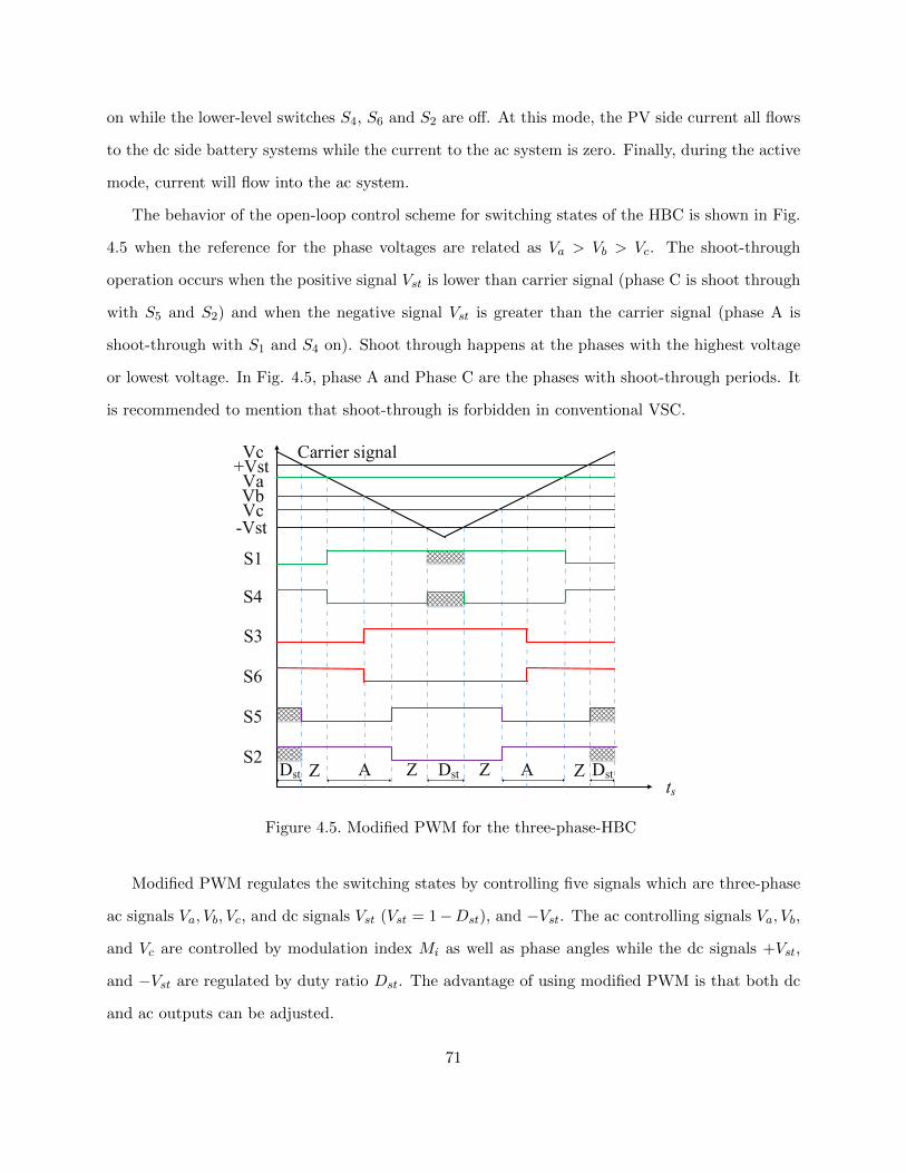
on while the lower-level switches S4
, S6
and S2
are o↵. At this mode, the PV side current all flows
to the dc side battery systems while the current to the ac system is zero. Finally, during the active
mode, current will flow into the ac system.
The behavior of the open-loop control scheme for switching states of the HBC is shown in Fig.
4.5 when the reference for the phase voltages are related as Va
> Vb
> Vc
. The shoot-through
operation occurs when the positive signal Vst
is lower than carrier signal (phase C is shoot through
with S5
and S2
) and when the negative signal Vst
is greater than the carrier signal (phase A is
shoot-through with S1
and S4
on). Shoot through happens at the phases with the highest voltage
or lowest voltage. In Fig. 4.5, phase A and Phase C are the phases with shoot-through periods. It
is recommended to mention that shoot-through is forbidden in conventional VSC.
+Vst
-Vst
VcVaVbVc
S1
S4
S3
S6
S5
S2
tsDst Dst DstZZ Z ZA A
Carrier signal
Figure 4.5. Modified PWM for the three-phase-HBC
Modified PWM regulates the switching states by controlling five signals which are three-phase
ac signals Va
, Vb
, Vc
, and dc signals Vst
(Vst
= 1Dst
), and Vst
. The ac controlling signals Va
, Vb
,
and Vc
are controlled by modulation index Mi
as well as phase angles while the dc signals +Vst
,
and Vst
are regulated by duty ratio Dst
. The advantage of using modified PWM is that both dc
and ac outputs can be adjusted.
71

4.2.5 Modeling of PV Array
Modeling PV cell can be obtained as a photo-generated current source in parallel with two
diodes and a shunt resistor, Rsh
, as well as in series with a series resistor, Rs
as shown in Fig. 4.6.
Two diode model of PV has more accurate performance than the single-diode model because it
represents di↵usion and recombination characteristics of the charge carriers in each cell [96].
Figure 4.6. Two diode model of PV
The following equations provide output current of a single PV’s cell:
Ipv
=Iph
Isat1
[eV
pv
+I
pv
R
s
1VT 1] I
sat2
[eV
pv
+I
pv
R
s
2VT 1] V
pv
+ Ipv
Rs
Rp
(4.4)
Iph
=Iph,STC
G
GSTC
[1 + ↵I
(T TSTC
)] (4.5)
VT
=kT
q(4.6)
Isat1
=C1
T
TSTC
31e
Egap
1kT (4.7)
Isat2
=C2
T
TSTC
52e
Egap
2kT (4.8)
where Iph
is the photo-induced current generated by the solar irradiation;Isat
is the reverse satura-
tion current; VT
is the thermal voltage of the PV module; T is cell temperature on Kelvin; ↵I
and
↵V
are temperature coecients of the current and voltage, respectively; k,q and are Boltzmann
constant, electron charge and diode ideality factor; Egap
and C1,2
are the band gap of the semi-
conductor material and temperature coecient; Rs
and Rp
are the equivalent internal and contact
resistances, respectively.
72

4.3 Control of PV Charging Station
This section provides a detailed explanation of the framework and controller of the HBC-based
PV charging station. From the steady-state relationship in (4.2), three-phase HBC utilizes Dst
to
boost the PV voltage while the modulation index Mi
regulates the ac voltage Vt
’s magnitude. In
addition, the angle of the three-phase ac voltage Vt
can be adjusted to achieve active power and
reactive power regulation. When the ac voltage is balanced and the ac system is symmetrical, the
total three-phase instantaneous power is constant at steady-state. Thus, average power of the ac
side equals to the net power at the dc side (Pac
= Ppv
Pdc
).
Three main control blocks are used to control the three-phase HBC: MPPT, phase-locked loop
(PLL) and vector control as shown in Fig. 4.7. Each block will be described in a subsection. The
charging algorithm of o↵-board dc/dc converter will also be addressed in this section.
Cpv
L
LfRf
idc
VdcCdc
Vpv
Ipv
PCC
+-
+-
ModifiedPWMMPPT PLL
DQABC
Vector ControllerVdc
*
Qac*
ƟPLL
Dst
iabc
Vdc
VsdVsq
idiq
Ipv Vpv
Vsabc
S1-S6
ƟPLL
Vsabc
Vtd
Ma
iabc
PHEV
PVDC bus
DQ
ABC
ABC
DQ
Vtq
Mb Mc
Idc
S1-S6
Figure 4.7. Control blocks of the HBC-based PV charging station.
4.3.1 Maximum Power Point Tracking (MPPT)
Maximum power point tracking (MPPT) algorithm is important to guarantee maximum power
extraction from PV arrays. Various types of MPPT algorithms have been recently applied to
control of MPP of PV modules. Hill climbing (HC), perturb and observe (PO), and incremental
73
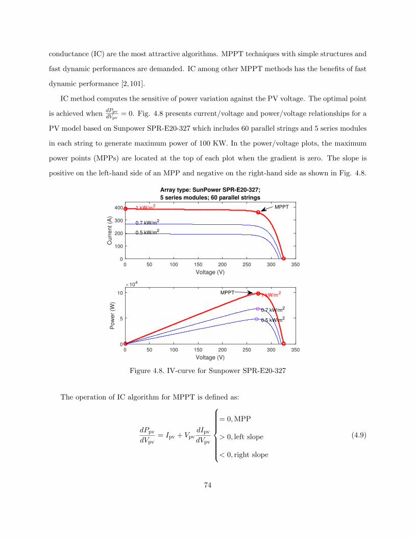
conductance (IC) are the most attractive algorithms. MPPT techniques with simple structures and
fast dynamic performances are demanded. IC among other MPPT methods has the benefits of fast
dynamic performance [2, 101].
IC method computes the sensitive of power variation against the PV voltage. The optimal point
is achieved when dPpv
dVpv= 0. Fig. 4.8 presents current/voltage and power/voltage relationships for a
PV model based on Sunpower SPR-E20-327 which includes 60 parallel strings and 5 series modules
in each string to generate maximum power of 100 KW. In the power/voltage plots, the maximum
power points (MPPs) are located at the top of each plot when the gradient is zero. The slope is
positive on the left-hand side of an MPP and negative on the right-hand side as shown in Fig. 4.8.
Voltage (V)
0 50 100 150 200 250 300 350
Cu
rre
nt
(A)
0
100
200
300
400 1 kW/m2
0.7 kW/m2
0.5 kW/m2
Array type: SunPower SPR-E20-327;
5 series modules; 60 parallel strings
Voltage (V)
0 50 100 150 200 250 300 350
Po
we
r (W
)
×104
0
5
10 1 kW/m2
0.7 kW/m2
0.5 kW/m2
MPPT
MPPT
Figure 4.8. IV-curve for Sunpower SPR-E20-327
The operation of IC algorithm for MPPT is defined as:
dPpv
dVpv
= Ipv
+ Vpv
dIpv
dVpv
8>>>>>><
>>>>>>:
= 0,MPP
> 0, left slope
< 0, right slope
(4.9)
74

Instead of using dPpv
dVpvas an indicator, the incremental conductance (IC) method relies on dIpv
dVpv.
The definition of IC method can be adjusted for better dynamic performance of the MPPT. Based
on the above relationship, we can also find that the following relationship:
8>>>>>><
>>>>>>:
Ipv
Vpv+ Ipv
Vpv= 0, optimal point (a)
Ipv
Vpv+ Ipv
Vpv> 0, left slope (b)
Ipv
Vpv+ Ipv
Vpv< 0, right slope (c)
(4.10)
The IC method requires to have the voltage deviation. When voltage deviation is very small, the
computed incremental conductance may not be accurate. It is observed that the error of comparing
the instantaneous conductance ( IpvVpv
) to the incremental conductance (Ipv
Vpv) does not achieve zero
at low irradiation [101].
To avoid using Vpv
in the denominator, [102] proposed a modified IC method. The modified
IC method is derived based on (4.9):
sign(dVpv
)dPpv
= sign(dVpv
)(Ipv
dVpv
+ Vpv
dIpv
)8>>>>>><
>>>>>>:
= 0,MPP
> 0, left slope
< 0, right slope
(4.11)
The control block of the modified IC based MPPT is shown in Fig. 4.9. The instantaneous con-
ductance will be added to the incremental conductance to generate an error signal. A proportional-
integral (PI) controller forces the error signal to approach zero. The output of the MPPT block is
subtracted from the reference duty cycle D to generate Dst
, which regulates the output dc voltage.
The subtraction is based on the relationship between Vpv
and Vdc
in (1a): Vpv
= Vdc
(1Dst
).
When the PV operation point is located as the left slope of the power/voltage curve, we would like
to have Vpv
be increased, or Dst
be reduced if the input signal is greater than zero. Therefore, the
subtraction is employed in the control block.
75

u
Ipv
Delay
Sign
PI
D*
Dst
dIpv
VpvdVpv
VpvudIpv+IpvudVpv
+
-
Delay
+
-
uu
+-
+
Figure 4.9. MPPT technique for PV using modified IC-MPPT method
4.3.2 Synchronous Rotating Reference Frame PLL (SRF-PLL)
The three-phase HBC is operated at grid-tied mode since the PV charging station needs ac
grid as a backup supply. Integration of the three-phase HBC has to satisfy IEEE-1547 standard
which requires synchrony of the phase and angular frequency of the three-phase HBC with the main
grid [52,103]. The controlling and designing of Synchronous rotating frame-based phase-locked-loop
(SRF-PLL) is presented in chapter 2.
4.3.3 Vector Control for PV Charging Station
Vector control technique is used for VSC. The inner loop controls the ac current while the outer
loop controls the dc voltage and reactive power. The dynamic equations of the three-phase HBC
are similar to those of the conventional VSC examined in [46,104]. The main di↵erence of HBC is
the consideration of Dst
. The inner current control loop is designed to respond much faster than
the outer voltage controller for fast response and disturbance rejection. It is suggested to achieve
fast transient response that the response of the inner loop to be in milliseconds, while the outer
loop is 10 times slower than the inner loop. The open-loop of the inner current loop includes the
transfer function of the plant and the delay of the modified PWM as well as the PI compensator.
Gi,ol
(s) =
K
pi
+K
ii
s
1
Lf
s+Rf
1
TPWM
s+ 1(4.12)
76

PI PI
PI
L
Vdc*
Vdc idc
id*
id
iq
Vsd
Vsq
DQ
ABC
MaMbMc
Qac*
ƟPLL
ωLf
ωLf
+
+
-
++
+
+
+-
-
-
++
+
-
Vtd
Vtq
2 Vdc3 Vsd
Vpv2(1-Dst)
-2 3Vsd
iq*
ipv
ModifiedPWM S1-S6
Dst
Figure 4.10. Vector control scheme of the three-phase HBC
where TPWM
is time delay of switching frequency of the modified PWM; Kpi
and Kpi
are the PI
compensator’s parameters for the inner current loop; Lf
and Rf
are the inductance and resistance
filter components of the converter, respectively.
Tuning current compensator is achieved by using modulus optimum technique [104]. The con-
cept of modulus optimum is defined as shifting the dominated poles that cause slow dynamic
response and achieving unity gain for the closed-loop system. The PI controller’s zero will cancel
the pole dominated by the RL circuit dynamics. The open-loop transfer function becomes
Giol
(s) =1
sTPWM
(TPWM
s+ 1)(4.13)
by choosing the following parameters: Kpi
=L
f
TPWM, K
ii
=R
f
TPWM.
One of the advantage of the proposed HBC-based PV station is to generate a supported reactive
power to the main grid. The controlling design of the reactive power loop is explained in details.
The delivered reactive power of the three-phase HBC at PCC is calculated as:
Qpcc
= 3
2Vsd
iq
(4.14)
where Vsd
is the projection of the ac voltage component on d axis of the stationary reference frame;
iq
is the projection of the output current of HBC on q reference frame. The open-loop transfer
77

function of the reactive power controller is given as follow:
Gol
(s) = GQ
(s)Gpi
(s)Gsw
(s)Gi
(s) = (3
2Vsd
)(kpQ
s+ kiQ
s)(
1
TPWM
s+ 1)(
1
Lf
s+Rf
) (4.15)
where kpQ
and kiQ
are the PI compensator’s parameters. Using modulus optimum technique on
Equ. (4.15), the open-loop and closed loop transfer functions of the reactive power are driven as:
Gol
(s) =1
Q
s(TPWM
s+ 1)(4.16)
Gcl
(s) =1
TPWM
Q
s2 + Q
s+ 1(4.17)
kp
=3
2
Vsd
Lf
Q
; ki
=3
2
Vsd
Rf
Q
(4.18)
where Q
is the time constant of the resultant closed-loop system. Equ. (4.17) represents a general
form of the second order system. The frequency of natural oscillation is obtained from Equ. (4.17)
to be equal !n
=p( 1
TPWM
Q
) while the damping factor equals =p
(
Q
4TPWM).
Assuming no switching power loss, the steady-state operation of the power balance is given as:
Ppv
= Pcap
+ Pdc
+ Pac
(4.19)
Pac
=3
2Vsd
id
(4.20)
where id
and Vsd
are the projections of the ac current and grid voltage space vectors on the d-axis.
The power relationship is further expressed as follows.
Pcap
= CVdc
dVdc
dt= P
pv
Pac
Pdc
= Vdc
Ipv
3
2Vsd
id
Vdc
Idc
Therefore, the dynamics of the capacitor voltage can be expressed as follows.
CdV
dc
dt= I
pv
3
2
Vsd
Vdc
id
Idc
| z u
d
(4.21)
78

A negative feedback controller will be designed to take in the dc voltage error V dc
Vdc
and amplified
by a PI controller. The output of the PI controller is ud
. From this signal, the reference signal id
will be generated as:
id
=2
3
Vdc
Vsd
(ud
Ipv
+ Idc
).
The open-loop transfer function of outer voltage is given as:
Gv,ol
(s) =
K
pv
+K
iv
s
1
i
s+ 1
1
Cs(4.22)
where i
is the time constant for the inner current closed loop. The open-loop transfer function for
voltage controller includes two poles at origin.
Symmetrical optimum is a technique to deal with an open-loop system with double integrators
[104]. The concept of symmetrical optimum is to operate the system at a low frequency to slow
down the dynamic response which leads to an increased phase margin. The compensator parameters
are given based on the symmetrical optimum method as follows.
Tiv
= a2i
, Kpv
=C
KpTiv
i
, Kiv
=K
pv
Tiv
(4.23)
where K equals 3V
sd
2Vdcand a is the symmetrical frequency range between peak phase margin and
low frequency operation area. It is important to select a high value of the symmetrical gain a to
achieve high phase margin. The value of a falls between 2 and 4 [105].
The frequency respond of the open loop of inner current controller and outer voltage loop are
designed by bode plot as shown in Figs. 4.11 and 4.12. The closed loop of the system is given in
Fig. 4.13. It can be seen from Fig. 4.13 that the bandwidth of the inner loop is higher than the
outer loop. So, the controller can response faster to the reference signal and provides stability.
4.3.4 O↵-board Battery Charger
Most of the PHEV manufacturers are recently using lithium-ion batteries to operate their
vehicles (e.g., Chevy Volt and Nissan Leaf). Since the PV charging station provides fast dc charging
79

Magnitu
de (
dB
)
-100
-50
0
50
100
100 101 102 103 104 105 106
Phase
(deg)
-180
-135
-90
-45
0
Plant
Compensator
Giol
Bode Diagram
Frequency (rad/s)
System: Giol
Phase Margin (deg): 65.5
Delay Margin (sec): 0.000251
At frequency (rad/s): 4.55e+03
Closed loop stable? Yes
Figure 4.11. Bode plot for open loop current controller
Magnitu
de (
dB
)
-100
-50
0
50
100
150
100 101 102 103 104 105 106
Phase
(deg)
-180
-135
-90
-45
0Plant
Compensator
Gvol
Bode Diagram
Frequency (rad/s)
System: Gvol
Phase Margin (deg): 53.1
Delay Margin (sec): 0.000556
At frequency (rad/s): 1.67e+03
Closed loop stable? Yes
Figure 4.12. Bode plot for open loop voltage controller
80

Ma
gn
itud
e (
dB
)
-100
-50
0
50
101 102 103 104 105 106
Ph
ase
(d
eg
)
-180
-135
-90
-45
0
Bode Diagram
Frequency (rad/s)
System: Gclv
Frequency (rad/s): 2.73e+03
Magnitude (dB): -2.99
System: Gicl
Frequency (rad/s): 7.04e+03
Magnitude (dB): -3.02
Figure 4.13. Bode plot for closed loop controller
procedure, it is important to investigate the model of lithium-ion batteries. An equivalent electrical
battery cell model is shown in Fig. 4.15. The battery model is composed of capacitor CCapacity
and
a current-controlled current source that represents the battery’s life. It also includes the Thevenin-
based model of the transient and steady-state elements as well as a voltage-controlled open circuit
voltage source. The dependent voltage source represents the amount of available energy in each
battery’s cell which is a function of the state of charge (SOC) of the battery. The modeling design of
PV charging station load requires aggregate the charged batteries of PHEV. This paper presents an
aggregated model of PHEV batteries that are connected in parallel for fast dc charging procedure.
Fig. 4.15 demonstrates the equivalent circuit of connecting PHEV batteries to the PV charging
station. The battery’s cells are connected in series to increase the voltage of the battery while the
parallel connection of the battery increases the total energy. So, each PHEV’s battery consists of
M branches and each branch consists of N cells. The detailed parameters of the commercial PHEV
can be found in [106].
Since a battery storage system is one of the most critical and expensive elements of PHEV,
charging control need to be carefully designed especially for fast charging process of PV station.
81

Fast charging technique may cause an excessive damage to the battery at the beginning of charging
process or increase the cell temperature if the battery reaches full charge and high current charging
is continued [107]. Standards such as the US NEVS and SAE J1772 [108, 109], mentioned that
controlling of o↵-board dc/dc converter is important for fast charging procedure.
Vbat
t
Ibat
Constant Current
(CC)
Constant Voltage
(CV)
Cut offCurrent
tcutoff
Energybat
Figure 4.14. A simple diagram of CC-CV technique for PHEV’s battery charging
In terms of charging schemes of a PHEV’s battery, constant-current (CC) charging, constant-
voltage (CV) charging, and taper-current (TC) charging are the three basic types of charging the
batteries [29,110,111]. CC charging method performs a relatively uniform current charging without
considering the battery state of charging (SOC) or temperature. The CC method mainly depends
on low or high constant charging current which helps eliminate imbalances of cells and enhances
life cycle of the battery. However, low charging current may not be acceptable to apply for dc fast
charging of PV station while too high charging current could easily catalyze an excessive damage at
the end of the charging procedure. Furthermore, CV procedure generally limits the voltage input
to a specific level regardless of the SOC of the battery. Implementing CV method requires the
knowledge of initial battery’s voltage to avoid the high potential di↵erence between the battery
and charger which causes a high initial current. This requirement is dicult to apply in real
82

applications of PV station since each PHEV’s has di↵erent battery’s characteristic. The concept of
TC charging method depends on decreasing the charging in proportion to the voltage rising of the
battery. The advantage of this method is that it prevents the gasification and overheat issues the
end of the fast charging process. However, the accuracy of implementing the charging procedure is
low in real applications due to the diversity characteristics between each of the PHEV’s batteries.R
discharge
Ccapacity
+
-
Ibattery
VocVbat
++
Rtrans Rseries
-
Ldc
Cdc
Sdc
Idc
Vbat*
Vbat
CC-CVSelector
-PI
>=
+Ich*-
PI
Ich
PWM
DC busdc/dc Converter PHEV Battery
ev
ei
Ddc
Ddc
Cutoff
Ctrans
Sdc
Figure 4.15. O↵-board charging structure using CC-CV algorithm
Considering the features of the each aforesaid methods, this paper introduces the integration of
constant-current and constant-voltage (CC-CV) methods to enhance the eciency and reliability of
the PV charging station. The procedure of implementing CC-CV on dc/dc converter is shown in Fig.
4.14 which mainly depends on controlling the charging voltage and current of battery at the same
time. The charging process depends on first charging the battery with constant current to avoid
the high initial current which is caused by a voltage di↵erence between the battery and charger.
When the battery’s voltage reaches the rated battery’s voltage, the controller switches to CV loop to
avoid overcharge. Finally, when the battery’s energy reaches the full charge region and the batteries
current reaches the cuto↵ line, the controller disconnects the PHEV for protection. Implementing
CC-CV method has several advantages such avoiding overheating issue and preventing overcharge.
83

When the charging procedure is operated at CC mode, the dc/dc converter charge the battery
with constant current until the voltage reaches its preset value. Then, the control method is
changed to CV mode for supplying a constant voltage. Finally, when the battery current reaches
the cute o↵ region, the dc/dc converter discount the PHEV’s battery to avoid overcharge. Fig.
4.15 shows two controlling loops are used to regulate the measured components of the battery and
the configuration of detailed PHEV battery and o↵-board dc/dc buck converter. The upper CV
loop is used for measuring Vbat
to avoid overcharging issue while the lower CC loop is applied for
Ich
to avoid overheating problem. The goal of the selector is to choose the operational mode of the
charger as well as discount the battery when it is the full charge.
4.4 Power Management and Operation Modes
Generating a sucient power to charge PHEV is controlled based on the operation level of DC
link voltage and the loading condition. The system is consist of a PV array as a main generating
source, three-phase ac grid as a supported source, and PHEV load. Measuring the DC bus voltage
and the available power from PV determine the procedure and direction of power flow management
using a proposed Vdc
vector control. This technique reduces the complexity of the controller as
well as provides eciency and stability of the system. The vector control which is derived and
explained in the previous section, play a major contribution in the selecting of operational mode
of the system.
Fig.4.16 shows the three operational modes of the PV charging station using a bidirectional
three-phase HBC. Since the three-phase HBC has the capability of being operated as converter or
inverter, controlling only a dc voltage across the dc bus can simplify the complexity of controlling
PV charging station. The operational modes of the system are categorized into three modes.
4.4.1 Mode I: PV Powers PHEV and the Utility
During a peak solar irradiation, the PV array extracts a maximum power which exceeds the
load’s demand. So, the bidirectional three-phase HBC delivers a required power to charge the
PHEV at DC bus as well as inverting the remaining PV power to the grid. The Vdc
vector controller
84

regulates the voltage at dc bus and supply the remaining PV power to the main grid. This mode
provides more reliability to the system since it generates the required power for charging electric
vehicles without the need for a power from the main grid.
4.4.2 Mode II: PV and the Utility Power the PHEV
In a case of low irradiance or high penetration of PHEV, the main grid participates in stabilizing
the voltage at dc bus. The bidirectional three-phase HBC is operated as a converter by absorbing
the grid’s ac power to charge the PHEV. In order to simplify the controller and avoid disturbance
during changing mode’s transient, the regulating of dc voltage using a proposed controller can
control the dc voltage at a specific value. As mentioned in the previous section, the outer loop
absorbs a power from the PV or the grid to regulate the voltage at dc bus. So, when the voltage
falls below the reference value, the controller absorbs a power from the main grid and send a signal
to the modified PWM. All the PV power is transferred to dc bus and the remaining required power
for charging a PHEV is generated from the utility. This mode can provide a stable charging as well
as enhance battery’s life of PHEV.
4.4.3 Mode III: The Utility only Powers the PHEV
The PV power does not generate any power during from midnight to sunset regarding absent
of solar irradiation. So, the vector control is changing to PQ control instead to Vdc
mode. The
bidirectional three-phase HBC operates only at converter mode to rectify the ac power and recharge
the PHEV. This mode always occurred at low ac load of the main gird.
4.5 Simulation Results
Case studies for a PV charging station using a three-phase HBC with the proposed control
are conducted in MATLAB/SimPowerSystems environment. The system’s parameters and PV
data are given in Table 4.1. The data for the PV model is based on PV array type Sunpower
SPR-E20-327. The V-I and P-V curves for di↵erent irradiance values are shown in Fig. 4.8.
The battery parameters of Chevrolet Volt and Nissan Leaf are used to represent the batteries of
85

PCC
DC Bus
HybridConverter
Ppv
Pdc
Pac
Grid
PHEV
PCC
DC Bus
HybridConverter
Ppv
Pdc
Pac
Grid
PCC
DC Bus
HybridConverter
Pdc
Pac
Grid
a) Ppv > PPHEV
b) Ppv < PPHEV
c) Ppv = 0
PHEV
PHEV
Figure 4.16. Operation modes of PV’s charging station
86

PHEVs [25,112,113]. Four case studies are conducted to evaluate MPPT and vector control as well
as to illustrate the operation modes and performance of the PV charging station.
Table 4.1. System parameters of a PV charging station
Parameters Parameters
PV
Voc
= 65.1 V
AC Side
Vgrid
= 20 kVLL
Vmpp
= 54.7 V ! = 377 rad/sIsc
= 6.46 A S = 100 kVAImpp
= 5.98 A Vph
= 208 VLL
Rsh
= 298.531 Rf
= 2 mR
s
= 0.369 Lf
= 125 µHLoad = 20 kW
DC Side
Vdc
= 350 V
AC/DC Control
Kpi
= 0.625 L = 5 mH K
ii
= 10 /sC = 12000 µF K
pv
= 0.24 1
Load = 100 kW Kiv
= 300 1/sLdc
= 10 mH Kpvdc
= 0.001Cdc
= 100 µF Kivdc
= 25K
iidc
= 0.001K
iidc
= 3
Chevy Volt
# of Cells: 200
Nissan Leaf
# of cells: 160Vcell
= 1.25 V Vcell
= 1.875 VQ
energy
= 16 kWh Qenergy
= 24 kWhType: Li-Ion Type: Li-Ion
4.5.1 Case 1: Performance of Modified IC-MPPT
The goal of this case study is to validate the performance of the modified MPPT using the
incremental conductance-PI algorithm. According to Fig. 4.8, the maximum PV power is 100
kW when the PV array generates 273.5 V at 1 kW/m2 solar irradiance. Fig. 4.17 shows the
performance of MPPT when the system is subject to solar irradiance variation. Di↵erent scenarios
of solar irradiance variation have been applied such as step change and ramp change.
The dc voltage Vdc
and the PV voltage Vpv
are related based on the duty cycle ratio Dst
that
is generated from MPPT. The role of vector controller is to keep the dc voltage Vdc
at its reference
value 350V and supply reactive power Qac
to the ac grid. The role of MPPT algorithm is to adjust
the duty cycle ratio Dst
and in turn adjust the PV output voltage Vpv
so that the PVs are operating
87

0 0.5 1 1.5 2 0.5
0.7
0.9
1.1
Su
n (
kW
/m2)
0 0.5 1 1.5 2 50
70
90
110P
V (
kW
)
0 0.5 1 1.5 2 0
0.25
0.5
Dst
0 0.5 1 1.5 2 200
250
300
350380
Time (sec)
Vo
ltag
e (V
)
MPPT OnMPPT Off
Vdc V
pv
Figure 4.17. Performance of a modified IC-PI MPPT algorithm
at the maximum power extracting point. Fig. 4.17 provides the performance of MPPT based on
four di↵erent intervals. From 0 0.5 seconds, the sun irradiance is 0.9 kW/m2 and the MPPT
control is not activated. The output PV power supplies approximately 70 kW. At t = 0.5 seconds,
MPPT is activated, the duty cycle ratio is decreased and the PV voltage is improved. This, in
turn, improves the PV power output to be 90 kW.
Note that whether the MPPT is on or o↵, Vdc
is kept at 350 V. At t = 1 second and t = 1.5
seconds, the sun irradiance increases and decreases. Due to the MPPT control, the optimal PV
output voltage is kept at the optimal level. Further, the PV output power tracks the maximum
point at each irradiance level. Fig. 4.17 validates the good tracking performance of MPPT when
di↵erent solar irradiations are applied to the PV. The simulation results also show that the vector
controller can regulate the dc voltage at 350 V and reject disturbances. This case study verifies
that the proposed MPPT algorithm can provide maximum performance during disturbances.
88

0 0.5 1 1.5 2 50
70
90
110
PV
(kW
)
0 0.5 1 1.5 2 0
0.25
0.5 D
st (
p.u
)
0 0.5 1 1.5 2 200
250
300
350
Vdc (
V)
0 0.5 1 1.5 2 100
200
300
Vpv (
V)
0 0.5 1 1.5 2 300
350
400
Time (sec)
I pv (
A)
MPPT On MPPT Off
Figure 4.18. Performance of the dc voltage control in the vector control
4.5.2 Case 2: Performance of the DC Voltage Controller
The advantages of implementing the three-phase HBC on PV charging station is its capability
to supply dc and ac power simultaneously. The main objective of a PV charging station is to supply
continuous dc power to electric vehicles. Case 2 investigates the ability of the proposed controller
to provide constant dc voltage with PV power variation and MPPT control status change.
Fig. 4.18 shows that when the dc voltage control is enabled, whether the MPPT control is
on or o↵ and whether the PV power has change or not, the dc voltage Vdc
is kept at 350 V.As a
comparison, when the dc voltage control is disabled and the MPPT control is o↵, the PV voltage
will vary. Since the MPPT control is o↵, the duty cycle ratio Dst
is kept constant and the dc
voltage Vdc
varies as well. This case study shows that the dc voltage control in the vector control
provides an additional measure to keep the dc voltage constant.
89

4.5.3 Case 3: Reactive Power and Grid Fault
Another advantage of the three-phase HBC control is that it can support the ac grid by supplying
or absorbing reactive power. The vector controller of PV charging station using three-phase HBC
is well designed in previous sections to achieve decouple controlling for real and reactive power.
This feature is applied in this case study to investigate the ability of the vector controller to quickly
track the reactive power reference as well as maintain a constant dc voltage. The system is first in
steady-state and the vector controller regulates the dc voltage and supply ac power at unity power
factor as shown in Fig. 4.19. At t = 0.5 sec the reference reactive power absorbs 10 kVAr while
at t = 1 sec it is changed to supply 10 kVAr to the main ac grid. The controller shows a good
performance to track the reactive power reference as well as regulate the dc voltage at 350 V. Fig.
4.19 illustrates that the vector controller’s Md
and Mq
respond to the reactive power variation.
0 0.5 1 1.5 2 Rea
ctiv
e P
ow
er (
kV
ar)
-20
-10
0
10
20
Q*
ac
Qac
0 0.5 1 1.5 2
Mi (
p.u
)
0
0.2
0.4
0.6
0.8
Time (sec)
0 0.5 1 1.5 2
Vd
c (
V)
345347349351353355357
Mq
Md
Figure 4.19. Performance of a proposed vector control using reactive power
Another important aspect of the three-phase HBC based PV charging station is its capability
to charge PHEV’s batteries during grid’s fault. The controller is designed to provide a stable dc
voltage even when grid fault is occurred. Generally, when the main grid voltage sages below 80%
of the nominal voltage, the power quality standards recommend to disconnect the charged PHEV
90

0 0.5 1 1.5 2
Vab
c(p
.u)
-1 -0.50 0.5 1
0 0.5 1 1.5 2
Po
wer
(kV
A)
-100
10
30
50
PHBC
Pac
Pload
Qac
0 0.5 1 1.5 2
Po
wer
(kW
)
50
70
90
110P
dc
Ppv
Time (sec)
0 0.5 1 1.5 2
Vd
c (
V)
345347349351353355
Figure 4.20. System performance under 50% grid’s voltage drop
to protect the battery’s life cycle [114]. The goal of designing the PV charging station’s controller
is to achieve constant charging procedure when a fault is occurred at the main grid. The method
of achieve this goal is to isolate the PHEV’s charger from the grid and provide sucient power
to charge the PHEV’s batteries as well as maintain constant dc-link voltage. As a result, it is
unnecessary to disconnect the PHEVs during grid fault.
The PV charging station is operated at steady state where the MPPT is not activated yet. The
PV station generates dc power to charge the PHEV’s batteries and satisfies the required the load
power. When the MPPT controller is activate at t = 0.5 sec, the remaining power is supplied to
the main ac gird as shown in Fig. 4.20. The main grid is facing a symmetrical 70% voltage sage at
t = 0.5 sec and both the dc bus voltage and the ac load are expected to be a↵ected. n nominal case,
it is recommended to disconnect the ac load as well as the PHEV’s batteries for protection and
safety manners. However, the proposed controller can mitigate this issue by stabilize the dc-link
voltage at its rated value as well as generate the required power to the local ac load. As also can
be seen in Fig. 4.20, the MPPT algorithm is still working during the voltage sage. However, Fig.
4.20 shows that the power from the grid is increased to compensate the decreased power across the
91

ac load. Therefore, the power is balanced across the system and the PV charging station is isolated
and can charge the PHEV’s batteries during a grid’s fault. When a partial grid fault is cleared at
t = 1 sec, the controller can reject the transient dynamic and achieve stable dc bus voltage.
0 0.5 1 1.5 2 340
350
360V
dc (
V)
0 0.5 1 1.5 2 −20
0
20
40
60
80
100
120
Time (sec)
Pow
er (
kV
A)
Qac
Leaf 1+Leaf 2 connected
Irradiance change
Volt 1 connected
Volt 2Connected
Ppv P
dc
Pac
Figure 4.21. Power management of PV charging station
4.5.4 Case 4: Power Management of the PV Charging Station
An objective of the HBC is to charge PHEVs even when there is not enough PV power. The
performance of the PV station is evaluated when di↵erent solar irradiations are applied. The goal
of case study is to show continuous charging PHEVs even when the PV power is low. At day time
the solar irradiance is assumed to be 1 kW/m2 while at sunset the irradiance equals to 0.7 kW/m2.
The dc load first consumes 50 kWh which represents charging of two Nissan Leaf vehicles. The
two Nissan Leafs are charged before the PV power decreases as shown in Fig. 4.21. The remaining
of PV power transfers to the main grid. At t = 0.5 seconds, the PV power reduces due to irradiance
change. Two more vehicles are connected to the system consequently at t = 1 seconds and t = 1.5
sec. Fig. 4.21 shows that the PV array can provide power to the third car at t = 1.5 sec. The PV
power is used to charge the batteries of PHEV with no dependency on the main grid.
92

At t = 1.5 seconds, the fourth electric car (Chevy Volt 2) is connected to the system. The a
bidirectional feature of the three-phase HBC and the regulated dc voltage controller allow the dc
load to absorb power from the main grid to charge the fourth vehicle as shown in Fig. 4.19. It is
also noticed that the three-phase HBC can achieve power balance as well as maintain constant dc
the voltage at 350 V. Fig. 4.21 also shows that the reactive power Qac
is kept at 0. This shows that
the three-phase HBC can achieve decoupled control of real and reactive power. Fig. 4.23 presents
the duty cycle ratio and the modulation index in dq-axes. Fig. 4.24 presents the detailed control
signals for modified PWM and the resulting switching sequences. This case study shows that the
proposed control can provide a smooth transition when PHEVs are connected into the PV station.
4.5.5 Performance of O↵-board dc/dc Converter
The CC-CV technique is applied to the proposed system to investigate the performance of the
controller. The CC method is first selected for fast dc charging with 40 A. The battery is continuous
charging unit it reaches 360 V which is the rated battery voltage of Chevy Volt vehicle [113]. When
the battery voltage is equal to 360 V at t = 2sec, the CV control is selected while the battery’s
current is gradually decreased up to the cuto↵ region.
0 0.5 1 1.5 2 2.5 3 3.5 4 4.5 5
Vch
(V)
280
300
320
340
360
Time (sec)
0 0.5 1 1.5 2 2.5 3 3.5 4 4.5 5
I ch(A
)
0
10
20
30
40
50
1.7 1.8 1.9 2
39
40
1.8 2 2.2
358
359
Figure 4.22. Performance of CC-CV algorithm
93

Time (sec)
0 0.5 1 1.5 2
Co
ntr
ol
Sig
nal
s (p
.u)
-0.1
0
0.1
0.2
0.3
0.4
0.5
Mq
Dst
Md
Figure 4.23. Dst
, Md
and Mq
for case 4
0.5 0.5005 0.501 0.5015 0.502 0.5025 0.503 0.5035 0.504 0.5045 0.505−1
−0.5
0
0.5
1
Co
ntr
ol S
ign
als
(p
.u)
Time (sec)
0.5 0.5005 0.501 0.5015 0.502 0.5025 0.503 0.5035 0.504 0.5045 0.505
0
1
0
1
0
1
0
1
0
1
0
1
Sw
itch
ing
Sig
na
ls
Time (sec)
Vst
−Vst
Va
Vb
Vc
phase A shoot through
phase C shoot through
Figure 4.24. The modified PWM signals and the switching sequences
94

CHAPTER 5
COORDINATION OF SMART INVERTERS
5.1 Introduction
Microgrid is a distributed network that provides controllable power and supporting energy by
interfacing distributed energy resources (DERs) with loads using power electronic mechanism. The
microgrid can be operated at grid-connected or autonomous modes. The DER units are operated
as grid-following (current controlled) or grid-forming (voltage-controlled) based on the connection
mode of the microgrid [115, 116]. The microgrid’s concept provides the opportunity to coordinate
di↵erent types of DER units based on their rated power. However, controlling an autonomous mi-
crogrid shows challenging problems such as the diculty to obtain equal power sharing and power
balancing between generation and load [117].
Load-sharing technique for an autonomous microgrid is commonly applied using droop control
method which mimics the behavior of a synchronous generator [55]. The concept of droop con-
trol depends on regulating the output voltage and frequency of DER unit based on the average
load ’s power. The advantages of droop control include high reliability and redundancy since the
communication between DER units is not required [118]. However, implementing droop control
requires an inherent trade-o↵ between power sharing accuracy and voltage and frequency regu-
lation. Regulating droop coecients may also impact the stability of the system because of the
slow dynamic response of droop control during the transient state. In [119], the authors confirm
that droop coecients influence on the stability of the system when the selected values of droop
coecients are closed the unstable region. The high value of droop coecients leads to reduce
the dynamic damping of the system which impacts the stability of the microgrid. Based on the
aforementioned challenges, achieving equal power sharing using droop control is very dicult due
95

to the mismatched line impedance and di↵erent power ratings of the DER units [120, 121]. Thus,
applying conventional droop controller to operate the autonomous microgrid may result in poor
reactive power sharing, severe circuiting current, and power coupling issues [122,123].
To realize accurate power sharing, several improved techniques on droop control have been pro-
posed in the literature. In [124], the authors propose adjusting droop coecients to improve power
sharing accuracy between DER units. However, droop coecients show poor dynamic response
when load power disturbance is applied. The virtual output impedance is proposed in [125] to
mitigate the impact of resistive line impedance and power coupling problems. Another proposed
concept is addressed in [126] by decoupling the output current and power using pre-measured de-
coupling impedance. The derivation of virtual impedance and decoupling impedance are developed
based on a simplified system which has considerable influence on the voltage quality due to frequent
load changing. Another approach is proposed in [127] which mainly depends on an adaptive droop
control. This technique can equally share the real load’s power and enhance the voltage profile.
However, the proposed method shows unequal reactive power sharing. The concept of master-slave
control is addressed in [128] where only one DER unit (master) is responsible for generating voltage
and frequency references while the other DER units (slaves) share the load power. The disadvantage
of this method is that it is dicult to connect another master unit which reduces the redundancy
of the system. A distributed secondary control is proposed in [129] by adding secondary control
unit at each DER units. This method increases the complexity and cost of the system. It also
requires central control unit for blackstart operation of an autonomous microgrid which reduces the
reliability of the system. An enhanced central controller is proposed in [130] by injecting reactive
and active power signals to reduce power sharing error. The central control monitors the behavior
of active power and sends reactive power error signal to mitigate power coupling issue. However,
this technique reduces the reliability of the system since it assumes no load disturbance during
correction phase.
In the aforesaid manuscripts, the circulating current is not considered in analyzing the per-
formance of the system at mismatched line impedance. Since droop control shows slow dynamic
response during transit mode, circulating current participates in providing more oscillation to the
96

system. In this paper, an improved technique is proposed to realize reactive power sharing and
mitigate the impact of circulating current when mismatched line impedance is presented. The novel
technique is not only achieving equal power sharing, but it can improve the stability of the system
by generating more dynamic damping during the transient state. The presented method consists
of two-level controller which are primary and secondary levels. In this context, a droop algorithm
is utilized at the primary control while an enhanced control microgrid unit (SCMU) is applied for
secondary control. Sharing the information between the primary controller of DER units is realized
via a communication bus. The advantage of the proposed method is that the knowledge of the line
impedance value is not required which provides the opportunity to operate medium or low voltage
microgrid where the line resistance is considered. The contribution of the paper lies in two aspects.
The first contribution is identifying the key factor that causes poor power sharing by analyzing the
mismatched line impedance issue. The derivation of circulating current is addressed based on the
steady-state analysis. The second contribution is designing of primary and secondary controllers
to operate an autonomous microgrid. The main purpose of designing the controller is to mitigate
the impact of circulating current and enhance the transient dynamics response.
5.2 Analysis and Modeling of an Autonomous Microgrid
Controlling an autonomous microgrid is a dicult task since the role of each DER units is not
only sharing the real and reactive powers but it also requires generating voltage and frequency.
This section addresses a review of the primary droop control and the microgrid’s configuration.
The analysis of reactive power sharing and circulating current due to mismatched line impedance
is presented in this section as well.
5.2.1 System Configuration
Fig. 5.1 shows a structure of the microgrid which is composed of DER units, local and global
loads, network line impedance, and the main utility grid. The microgrid is connected to the main
utility grid through the point of common coupling bus (PCC). DER units are connected to the
local loads by dc/ac two-level three-phase converter (VSC), LC filter, and network line impedance.
97

When there is a fault or scheduled maintenance at the main grid, the static transfer switch (STS)
is opened by a signal command from SCUM as presented in Fig. 5.1. The microgrid is then op-
erated at autonomous mode while the SCUM changes the operational situation of DER units to
grid-forming mode. This mode requires DER units to provide voltage and frequency to the local
and global loads as well as sharing the total load power.
VSI1
Controller
RLC Filter Line Network
Local Loads
Line N
etwork
STS
Main Grid
SCUM
Global Loads
Low-bandwidth Bus
PCC
DER1
TransmitterReceiver
iabc1
vabc1 voabc1
ioabc1
Lf1 Rf1
Cf1Ln1 Rn1
Ln
Rn
Vdc1
VSI2
ControllerRLC Filter Line
Network
Local Loads
DER2
TransmitterReceiver
iabc2
vabc2
ioabc2
Lf2 Rf2
Cf2Ln2 Rn2
Vdc2
iload
igrid
Figure 5.1. Single line-configuration of a microgrid
Controlling DER units is achieved by a hierarchal control which consists of primary and sec-
ondary central controls. The primary control includes droop control, cascaded inner voltage and
current control loops as shown in Fig. 5.2 b. The main role of droop control is to regulating voltage
and frequency of the microgrid based on the average output power. The cascaded inner voltage and
frequency loops are designed to reject the high frequency disturbance as well as generate a terminal
voltage reference for controlling switches of VSC. The role of secondary SCUM is to regulate the
terminal output voltage of the primary droop control to achieve equal power sharing. Fig. 5.2
b shows a linearized model of the output voltage using hierarchal control. The figure shows that
98

SCUM injects a regulated voltage signal V s
Q
to achieve reactive power sharing and mitigate the
circulating current which will be illustrated in section 5.3.
VSI
Communication Bus
PCC
iabc
vabc1voabc
ioabc
Lf Rf
pq
Ln RnVdc +
-
Power Calculation
DroopControl
VoltageControl
PWMIdq
. . . .S1-S6
Vdq
PQ ioabc
voabc
VQs
Low-passFilter
PQs
Transmitter/Receiver
Cf
vabc
abcdq
iodq
vodq
CurrentControl
∫
ω
θ
θ
abcdq
* *
vodqiodq
Mdq
θ
mabc
voioif
io
PWMCurrentControl
vcVoltageControl
DroopControl
vo if*
PowerCalculation & Filtering
P
Q
+ + + + -
-
--
vQ
+
vo
s
f f
Lf s+Rf
* 1 o
Cf s1*
*
a b
Figure 5.2. Block diagram of the autonomous microgrid
5.2.2 Control of Smart Inverter Using Primary Droop Control
This section demonstrates the concept of droop control as well as designs the vector controller
for DER unit. Droop control is often implemented when at least two DER units are connected in
parallel to form a microgrid. The primary control of each DER involves dual voltage and current
control loops and droop algorithm as shown in Fig. 5.2 b. The output signal from the droop control
is transferred to the cascaded inner loops to generate VSC’s switching commands using PWM.
Since the microgrid contains multiple DER units, the system can be represented as multi-input
and multi-output system. The DER units are operated as grid forming mode by generating voltage
and frequency to the load. From Fig. 5.1, the power flow equation between DER and PCC is
analyzed based on power flow equations as:
Si
= 3Voi
Ioi
(5.1)
Pi
=3(R
ni
V 2
oi
Rni
Voi
Vpcc
cos i
+Xni
Voi
Vpcc
sin i
)
R2
ni
+X2
ni
(5.2)
Qi
=3(X
ni
V 2
oi
Xni
Voi
Vpcc
cos i
Rni
Voi
Vpcc
sin i
)
R2
ni
+X2
ni
(5.3)
99

where Si
is the apparent power of the ith DER unit; Pi
and Qi
are the output real and reactive
powers, respectively; Voi
and Ioi
are the output phase voltages and currents from ith DER unit;
Vpcc
is the voltage across PCC bus; Rni
and Xni
are the resistance and inductance line impedances;
i
is the phase angle voltage di↵erence between DER unit and PCC.
In order to simplify the concept of droop control, it is assumed that the line impedance (X/R)
ratio is high; so the line resistance impedance can be ignored. Equations (5.2) and (5.3) are then
modified based on the previous assumption where the output real power regulates the output
frequency and the reactive power controls the output voltage magnitude as illustrated below:
Pi
=3V
oi
Vpcc
Xni
sin(i
) (5.4)
Qi
=3(V 2
oi
Voi
Vpcc
cos(i
))
Xni
(5.5)
Equations (5.4) and (5.5) show that the real power is proportional to the voltage phase angle while
the reactive power is related to the voltage di↵erence magnitude between DER units and PCC bus.
Accordingly, the proportional droop gains are used to generate the voltage and frequency as:
!i
= !i
kPi
Poi
(5.6)
Voi
= V i
kQi
Qoi
(5.7)
where !i
and !i
are the output frequency and the rated frequency of the microgrid; Voi
and V i
are the output phase and the preset voltages; kPi
and kQi
are the droop coecients for frequency
and voltage controllers.
In conventional droop control, the constant droop coecients kPi
and kQi
are selected based
on the deviation of the output voltage and frequency over the maximum power [131]. The optimal
value of droop coecients are derived as:
kPi
=!max
!min
Poi
max
(5.8)
kQi
=Vmax
Vmin
Qoi
max
(5.9)
100

Vector control methodology is used to control the voltage and frequency of VSC. The concept
of vector control depends on transferring symmetrical signals from three-phase time domain into
two-phase rotating synchronous reference frame DQ [132]. Fig. 5.2 a is analyzed to model the
primary droop control and inner voltage and current loops. The dynamic equations of the system
are represented in synchronous rotating reference frame DQ as following:
didqi
dt=
Rfi
Lfi
idqi
± !0
iqdi
+1
Lfi
(vdqi
vodqi
) (5.10)
dvodqi
dt= ±!
0
voqdi
+1
Cfi
(idqi
iodqi
) (5.11)
diodqi
dt=
Rni
Loi
iodqi
± !0
inoqdi
+1
Lni
(vodqi
vpccdq
) (5.12)
where vdqi
and idqi
are the filtered voltages and currents of inner loops of ith DER unit at DQ axes;
vodqi
and iodqi
are the output voltages and currents of ith DER unit at DQ axes; vpccdq
are the
voltages on PCC bus; Rfi
, Lfi
, and Cfi
are the resistance, inductance, and capacitance components
of LC filter; Rni
and Lni
are the resistance and inductance of the line impedance between DER
unit and PCC bus.
Vector control is used to calculate the instantaneous real and reactive powers. As shown in Fig.
5.2 a, equations (5.4) and (5.5) are adjusted based on the output voltages and currants as:
pi
=3
2(v
odi
iodi
+ voqi
ioqi
) (5.13)
qi
=3
2(v
odi
ioqi
+ voqi
iodi
) (5.14)
The droop coecients have a proportional relationship with the load power. The measured instan-
taneous output powers are not sucient to be applied for droop control. So, a low-pass filter is
used to extract the average active and reactive output powers as shown below:
Pi
=!c
s+ !c
pi
(5.15)
Qi
=!c
s+ !c
qi
(5.16)
101

where !c
is the cuto↵ frequency of low-pass filter. The operation of filtering the instantaneous
output power is given in power calculation block in Fig. 5.2 a. Since the output voltage contains
two components on DQ axes, the magnitude of the output phase voltage is obtained as:
|Voi
| =qv2odi
+ v2oqi
(5.17)
It is recommended to mention that the concept of vector control aims to align the output voltage
on D axis which leads to voiq
= 0. So, the output phase voltage will equal the voltage on D axis.
The derivation of droop coecients depends on a balanced system which defines as total gen-
erated power from DER units should equal the total required power from the loads. Selecting
optimal value of droop coecient on equations (5.8) and (5.9) needs to consider an inherent trade-
o↵ between voltage and frequency regulation and power-sharing accuracy. Fig. 5.2 a shows that
a low-pass filters are used to calculate the average value of the active and reactive powers. These
main components of droop control need to be carefully designed to avoid stability issues [133].
Poor designing of droop coecients kPi
/kQi
and cuto↵ frequency !c
leads to reduce the dynamic
damping response as well as generate unequal reactive power sharing and circulating current.
5.2.3 Reactive Power Sharing
This section analyzes the key factor that influences on the accuracy of reactive power sharing.
As shown in Fig. 5.3, the power sharing between DER and the rest of the microgrid depends on
the characteristics of the line impedance. The voltage drop across the line impedance is analyzed
based on the output powers and voltages of each DER. Since the voltage angle frequency is a global
variable, sharing active power can be achieved by properly selecting an accurate kPi
coecient of
the P ! droop control as given in equation (5.4). However, equally sharing the reactive power
cannot be achieved by only tuning the kQi
gain of the (Q V ) droop control as seen in equations
(5.5) and (5.9). The reason is that the reactive power depends on the voltage di↵erence between
the output voltage of DER unit and the voltage across PCC bus. So, the voltage drop on the line
impedance influences on the reactive power sharing when there is a mismatched line impedance.
102

Vdrop1
Global Loads
PCCDER2
DER1PQ1
io1
io2
Ln1 Rn1 δLn δRn
Vdrop2
Ln2 Rn2
δV
vo1 θ1
PQ2
vo2 θ2
vpcc 0
iload
icc1
icc2
+
-
Figure 5.3. Simplified two-DER units microgrid with mismatched line impedance
Because of the complexity of the microgrid, it is assumed that the two DER units have identical
power capacity and the local and global loads have no impact on the reactive power sharing. A
simplified two DER units microgrid is shown in Fig. 5.3. Each DER unit is designed as an ideal
voltage source. The output voltage of DER unit Voi
is a factor of wire and internal impedance, DC
voltage, fundamental frequency and amplitude voltage component. The voltage drop on the line
impedance is calculated as [55]:
Vdrop1
Xn1
Q1
+Rn1
P1
Vo1
(5.18)
Vdrop2
Xn2
Q2
+Rn2
P2
Vo2
(5.19)
where Vdrop1
and Vdrop2
are the drop voltages on the two di↵erent line impedances; Xn1
, Xn2
, Rn1
and Rn2
are di↵erent values of the inductance and resistance of the line impedances. Assuming the
line impedances of the two DER units are given from Fig. 5.3 as:
Xn1
= Xn2
+ X (5.20)
Rn1
= Rn2
+ R (5.21)
where X and R are the mismatched line inductance and resistance between two DER units.
103

By adding the mismatched line impedance into equations (5.18) and (5.19), the output voltage
is calculated based on Fig. 5.3 as:
Vdrop1
(Xn1
+ X)Q1
+ (Rn1
+ R)P1
Vo1
(5.22)
Xn1
Q1
+Rn1
P1
Vo1
+XQ
1
+ RP1
Vo1
(5.23)
Vo1
= Vpcc
+ Vdrop1
+ V (5.24)
Vo2
= Vpcc
+ Vdrop2
(5.25)
where V is the voltage drop across the mismatched line impedance. It is noticed from equations
(5.24) and (5.25) that the voltage across PCC (Vpcc
) is facing two di↵erent values of the voltages
from DER units because of the mismatched voltage drop (V ). These voltages will produce di↵erent
values of reactive power across PCC bus [134, 135]. The output reactive power can be given by
rewriting equation (5.7) as:
Qi
=V oi
Voi
kQi
(5.26)
Based on the aforesaid equations (5.20)-(5.26), three variables may impact on the reactive power
sharing accuracy which are the mismatch line impedance, the output voltage di↵erence magnitude
between DER units, and the reactive droop coecient. In real applications, achieving identical
line impedance between DER units is a dicult task due to the distance di↵erence and locations
of DER units. Besides, increasing the droop gain kQi
may reduce the reactive power based on
equation (5.26). However, a large value of the droop coecient causes large voltage variation from
the nominal value [136]. This variation is restricted with a limitation of voltage amplitude deviation
of each unit which has to be 10% of the nominal voltage according to IEEE standards [52]. In fact,
the mismatched voltage drop could not be mitigated by only regulating the droop factor kQi
. The
reason is that the droop factor is proportional to the load power and any disturbance may lead to
change the output voltage of DER unit. Another feasible solution is to adjust the output voltage
di↵erence magnitude between DER units which can achieve balanced voltage at PCC. Regulating
104

the voltage di↵erence between the output DER voltage and the reference voltage may reduce the
reactive power error as seen in equations (5.24) and (5.25).
The linearized model in Fig. 5.2 b shows that injected voltage V s
Q
can compensate the impact
of the line impedance’s drop voltage V by regulating the output voltage of the primary droop
control. Hence, equation (5.24) can be driven as:
Vo1
+ V s
Q1
= Vpcc
+ Vdrop1
+ V (5.27)
where V s
Q1
is the injected voltage from the central controller (SCUM). The operation and design
of the SCUM will be demonstrated in section 5.3. If the controller is well design to mitigate the
impact of the mismatched voltage drop, the output voltage of equation (5.24) is given as:
Vo1
= Vpcc
+ Vdrop1
, V s
Q1
= V (5.28)
The unequal reactive power sharing appears because of the di↵erent voltage drop across the
mismatch line impedance. This mismatched line voltage V will generate a circulating current
between DER units. Equation (5.27) points out the injected voltage from SCUM V s
Q
can compensate
the mismatched line voltage V by adjusting the output voltage of DER units.
5.2.4 Circulating Current Analysis
The mismatched line voltage V presents a poor power sharing which generates the circulating
current between units. The relation between circulating current and reactive power is given as:
Si
= 3Voi
Ioi
= 3Voi
(Voi
Vpcc
Zni
) (5.29)
In [138], the authors define the circulating current between two DER units as:
Icc1
=Io1
Io2
2(5.30)
Icc2
=Io2
Io1
2(5.31)
105
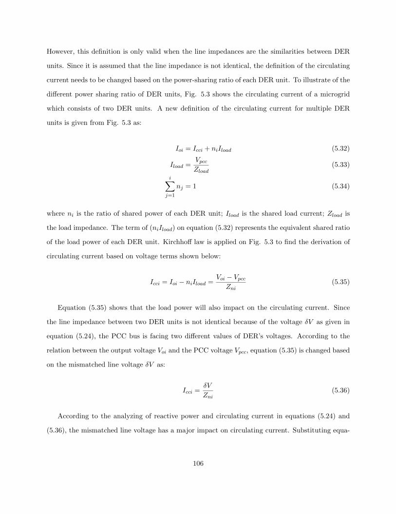
However, this definition is only valid when the line impedances are the similarities between DER
units. Since it is assumed that the line impedance is not identical, the definition of the circulating
current needs to be changed based on the power-sharing ratio of each DER unit. To illustrate of the
di↵erent power sharing ratio of DER units, Fig. 5.3 shows the circulating current of a microgrid
which consists of two DER units. A new definition of the circulating current for multiple DER
units is given from Fig. 5.3 as:
Ioi
= Icci
+ ni
Iload
(5.32)
Iload
=Vpcc
Zload
(5.33)
iX
j=1
nj
= 1 (5.34)
where ni
is the ratio of shared power of each DER unit; Iload
is the shared load current; Zload
is
the load impedance. The term of (ni
Iload
) on equation (5.32) represents the equivalent shared ratio
of the load power of each DER unit. Kirchho↵ law is applied on Fig. 5.3 to find the derivation of
circulating current based on voltage terms shown below:
Icci
= Ioi
ni
Iload
=Voi
Vpcc
Zni
(5.35)
Equation (5.35) shows that the load power will also impact on the circulating current. Since
the line impedance between two DER units is not identical because of the voltage V as given in
equation (5.24), the PCC bus is facing two di↵erent values of DER’s voltages. According to the
relation between the output voltage Voi
and the PCC voltage Vpcc
, equation (5.35) is changed based
on the mismatched line voltage V as:
Icci
=V
Zni
(5.36)
According to the analyzing of reactive power and circulating current in equations (5.24) and
(5.36), the mismatched line voltage has a major impact on circulating current. Substituting equa-
106

tions (5.35) and (5.36) into equation (5.29), the total output power from DER units at mismatched
line impedance is given as:
Soi
= 3(Voi
+ V )(Icci
+ ni
Iload
) (5.37)
= 3
Voi
(V
Zni
) + Voi
ni
Iload
+V V
Zni
+ V ni
Iload
(5.38)
Equation (5.38) shows that the voltage drop across the mismatched line impedance presents addi-
tional terms on the output DER’s power. The output complex powers include actual power and
circulating-current power which is driven from equation (5.38) as:
Soi
= 3Voi
ni
Iload
(5.39)
Scci
= 3
Voi
(V
Zni
) +Voi
V
Zni
+ V ni
Iload
(5.40)
This section verifies that the mismatched line voltage generates the poor reactive power sharing
and circulating current. When the secondary controller SCUM achieves to compensate the mis-
matched line voltage V = 0, the circulating-current power will disappear as shown in equation
(5.40). Thus, the complex output power consists only the actual load’s power. So, designing suf-
ficient central controller needs also to reject the impact of the load disturbance on the circulating
current as shown in equation (5.35).
5.3 Proposed Secondary Control
5.3.1 Concept and Topology
Coordination of parallel DER units using droop control may cause a couple of issues such as
poor reactive power sharing and circulating current. Due to the impact of network impedance,
conventional droop control provides a poor reactive power sharing. Circulating current analysis
shows that voltage drop V has a huge impact on the reactive power sharing. So, secondary central
control is implemented using SCUM to reject the impact of mismatched line voltage V . The sec-
ondary control SCUM is realized by communication bus to achieve equal reactive power sharing.
107

vdc
md
mq
L ω
L ω
vq
vd
id
iq
C ω
C ω
ilq
ild
vod
*
1.5× vod×ioqvoabc
ioabc
DQ
ABC
mabc
DQ
ABC
DQ
ABC
vodq
iodq 1.5× vod×iodp P
kP
Q1
Qi∑ j=1 Qj VQ
÷
÷
q QkQ
0
vod
voq
θ ω*
VQ
V*
Primary Control
dc
d
q
L ω
L ω
vq
d
d
iq
C ω
C ω
ilq
ld
od
voabc
oabc
od oq
DQmabc
ABC
DQ
vodq
iodq 1.5× vod×iodp
kPk
÷
÷
od
oq
θ ω*
VQVV
1
ij=1 j VQVV
Secondary Control
-+
-+
-+
-+
++
-+
-+
=+
+
1s
-+
-+
+
Q2
Qi
.
.
. i
i
Selector
s
θ
θ
s
Communication Bus
Communication Bus
ωcs+ωc
ωcs+ωc
*
voq
kpv+kiv
s
kpv+kiv
s
kpi+kii
kpi+kii
s
s
kpi+kii
skpikk + ii
Limiter
++
-
-+
-
Figure 5.4. Detailed primary and secondary controllers for autonomous microgrid
The detailed controlling block diagram of controlling the microgrid is shown in Fig. 5.4 which
includes primary and secondary controllers. The primary control measures the output voltage and
frequency to calculate the average powers. The average powers are extracted using a low-pass filter
with a bandwidth frequency (!c
). The reference voltage and frequency are then determined based
on assigned droop gains based on the vector control concept on Fig. 5.4. The cascaded inner loops
are controlled on DQ reference frame using PI compensators. The controller is implemented in
synchronous rotating frame DQ as shown in Fig. 5.4. Designing the cascaded inner loops can be
found in [139], being out of the scope of this paper. Each DER unit needs to calculate average
powers to share the information with the SCUM via a communication bus. The SCUM calculates
the average reactive power and sends the corrected voltage ksiQi
to the primary control.
108

The simple design of proposed controller aims to decrease the cost and complexity of the system.
As shown in equation (5.35), load changing influences on the circulating current. Thus, design PI
controller of the SCUM requires achieving disturbance rejection as well as equal reactive power
sharing. It is important to mention that when there is an error in transmitting the information
using communication bus, the microgrid still generating voltage and frequency using the primary
control.
Sharing the information between SCUM and DER units is achieved via the communication
bus. Each DER unit needs to calculate the average output power from the primary control and it
to SCUM. The corrected voltage reference SCUM V s
Qi
is transmitted back to each DER unit via
communication bus as shown in Fig. 5.4. This voltage can mitigate the impact of mismatched line
voltage even at frequent load disturbance. This technique can also be used for high or low R/X
microgrid since it does not require information of the line impedance. Generally, the bandwidth
of communication link has to decrease in higher levels of controlling a microgrid. Since the trans-
ferred signals are averaged and fundamental, low-bandwidth communication is only required for
transferring information. This feature can reduce the cost of communication bus as well as increase
the reliability of the microgrid.
5.3.2 Controlling Strategy
The averaged reactive power of all DER units is calculated by SCUM and compared with the
fundamental output power from each DER unit via low-bandwidth communication bus as shown
in Fig 5.4. The error between the average reactive power and the fundamental reactive power is
regulated by PI compensator of the SCUM. PI controller guarantees that the steady state error
equals zero. The selector block aims to identify each signal from DER unit in order to generate a
corrected voltage. The regulated voltage V s
Q
i
is calculated based on the following equation as:
V s
Q
i
= kspQi
(QQoi
) + ksiQi
Z(QQ
oi
)dt (5.41)
Q =
Pi
j=1
Qoj
i(5.42)
109

where V s
Q
i
is the injected voltage from SCUM to each ith DER unit; kspQi
and ksiQi
are the parameters
of PI compensator of SCUM; Q is the average reactive power required by the load.
The control block diagram of the reactive power loop with voltage profile using SCUM and
primary control is shown in Fig. 5.5. The reactive power control includes SCUM to process equal
power sharing by comparing the error of calculated average reactive power with the measured
power. The primary control has been modeled based on equation (5.9) where a low-pass filter (!c
)
is applied to extract the fundamental reactive power from the instantaneous one.
eVpcc VQ+
V*
Qi
QiGLPFKQi
++
+-Vpcc Q
SCUM
Qpcc* GQs -H
Vis
Figure 5.5. Block diagram of reactive power control
The block diagram of the voltage control using SCUM and primary control is shown in Fig.
5.5. The figure shows the controlling technique for reactive power control. The SCUM monitors
the average reactive power at PCC and sends a corrected voltage to gain equal power sharing. The
closed-loop characteristic of reactive power control is given from Fig. 5.5 as:
Qi
=HV
1 +HGQs
HkQi
GLPF
+HG
Qs
1 +HGQs
HkQi
GLPF
Qpcc
(5.43)
where
GV
s = GQs
= kspQ
+ksiQ
s,G
LPF
=!c
s+ !c
H =Voi
Voi
Vpcc
cos(i
)
Xni
110

5.4 Simulation Results
The mismatched line impedance presents poor reactive power sharing and circulating current
when droop control is applied. The circulating current adds more oscillation to the microgrid since
the droop control shows a slow dynamic response. This section simulates the proposed method in
order to verify the analysis of the circulating current. The performance of the proposed method is
investigated at two operational situations of the system which are stable and oscillator modes. The
proposed controller needs to provide equal power sharing during steady state as well as improve
the dynamic response during the transient state. The realization of primary and secondary control
is achieved via low-bandwidth communication bus.
Table 5.1. System parameters of three DER units forming autonomous microgrid
Symbol Value Unit Comment
S 10 KVA Power Rating for DER units.Vo
120 V Nominal Phase Voltage for the microgrid.! 377 Hz Nominal Frequency for the microgrid.Vdc
500 V Dc-link Voltage for DER units.Fs
5 kHz Switching Frequency for DER units.Lf
5 mH Filter Inductance for DER units.Cf
250 uF Filter Capacitance for DER units.Ln1
0.5 mH Line Inductance for first DER unit.R
n1
200 m Line Resistance for first DER unit.Ln2
1.5 mH Line Inductance for second DER unit.R
n2
600 m Line Resistance for second DER unit.Ln3
1 mH Line Inductance for third DER unit.R
n3
400 m Line Resistance for third DER unit.R
load
10 kW Global Linear Load
Implementing central controller (SCUM) of the microgrid in Fig. 5.1 is modeled in Mat-
lab/SimPowerSystems software. The system and control parameters are listed in Tables 5.1 and
5.2. The system includes three DER units to generate voltage and frequency as well as sharing
the load power. A mismatched line network is presented in Table 5.1 by assigning di↵erent values
of each line impedance. It is assumed that the three DER units have similar power ratings. So,
the controlling parameters of the primary and secondary controllers for the three DER units are
111

Table 5.2. Control parameters of primary and secondary controllers
Symbol Value Unit Comment
kP
0.05-0.0.5 mHz/W (P !) Droop for DER units.kQ
1-1.5 V/Var (V Q) Droop for DER units.kpi
33.3 Proportional Gain for Current Loop.kii
266.7 /s Integral Gain for Current Loop.kpv
0.56 1 Proportional Gain for Voltage Loop.kiv
411.5 1 /s Integral Gain for Voltage Loop.!c
30 Hz Cuto↵ FrequencykspQ
0.01 uF Proportional Gain for SCUM Loop.
ksiQ
0.5 mH Integral Gain for SCUM Loop.
n1
0.576 Ratio of Power for First DER unit.n2
0.385 Ratio of Power for Second DER unit.n3
0.0385 Ratio of Power for Third DER unit.
identical. Two case studies are given in this section to investigate the performance of the proposed
system based on circulating current and reactive power analysis.
5.4.1 Case1: SCUM Operation
Circuiting current and unequal reactive power sharing have commonly appeared when mis-
matched line impedance is considered between DER units. Droop coecients are carefully selected
based on the power rating of each DER unit. As seen in Fig. 5.6 a, equal real power sharing is
achieved by selecting optimal values of power droop gain as given in equations (5.8) and (5.9).
However, Fig. 5.6 b shows a huge di↵erence of the output reactive powers of DER units. This
circulating reactive power may overheat the VSC devices as shown in Fig. 5.6 b, when the second
DER unit absorbs 3000V ar of reactive power. The ratio factors of power-sharing of DER units
are calculated based on the power-sharing as given in Table 5.2. The di↵erent power ratios which
are caused by mismatched line impedance, are used to calculate the circulating current. The cir-
culating current equals 5A based on equation (5.32). The voltage drops on the line impedances of
DER units are calculated using equation (5.18) which equal 18V , 35V , and 26V , respectively. So,
the mismatched impedance voltage is calculated from equation (5.24) which equals 9V. This value
generates 5A circulating current which needs to be mitigated to achieve equal power.
112

0 0.5 1 1.5 2 2.5 3 3.5
a
4 6 8 1012
P (
kW
)
... DER1 --- DER
2 DER
3
0 0.5 1 1.5 2 2.5 3 3.5
b
-3
0
3
Q (
Kv
ar)
0 0.5 1 1.5 2 2.5 3 3.5
c
110
120
130
140
Vrm
s (V
)
0 0.5 1 1.5 2 2.5 3 3.5
Time (s)d
-202468
I cc (
A)
Figure 5.6. Simulation results for case 1 at stable system
To prevent this dangerous circulating current, SCUM is activated at t = 0.5sec by measuring
the output average reactive powers and sending a corrected voltage to DER units via the commu-
nication bus. This injected voltage compensates the impact of mismatched line voltage V which
is calculated to equal 9V . Regulating the reactive power is applied using the PI controller while
the control signal regulates the output voltage reference of the primary control of each DER unit.
By applying SCUM, the mismatched voltage drop V is mitigated and equal reactive power is
achieved as shown in Fig. 5.6 b. Fig. 5.6 d, shows that the circulating current is reduced to 0A.
Fig. 5.6 c, shows the output voltages of DER units. Even these values are di↵erent because of the
113

mismatched line impedance, the proposed controller can mitigate V which verifies the analysis in
subsection 5.2.3. The variation of the voltages is within the 10% limitation of the rated voltage as
it is recommended by IEEE standards.
The advantage of the proposed controller is achieving equally reactive power sharing even when
the load is a disturbance. As given in equation (5.35), disturbance in the load leads to chang-
ing the circulating current. Fig. 5.6 shows an additional 10kW load is connected to the system at
t = 1.5sec. This load disturbance activates the controller in SCUM to regulate the voltage reference
on droop controller for each DER unit. Even when the second load is disconnected at t = 2.5sec,
the SCUM can achieve equal reactive power sharing as well as remove the circulating current.
5.4.2 Case2: SCUM Operation Under Ocillator System
This paper claims that the proposed controller SCUM cannot only achieve equal power sharing,
but it can provide more damping to the system during the transient state. Circulating current
generates more oscillation to the system when the droop coecients and low-pass filter of the
primary control are not well designed. This case study aims to identify the behavior of the microgrid
when the system has high oscillation based on the circulating current. The high value of droop
parameters and the high circulating current reduce the dynamic damping of the system when
disturbance is applied to the microgrid. The droop coecients for the three DER units kP
and kQ
are increased from 0.05 to 0.5mHz/W and 0.1 to 1.5mV/V ar, respectively. This increasing reduces
the dynamic damping response of the system which a↵ects dynamic response at any disturbance.
Fig. 5.7 a, shows the system is operated at steady state. A load disturbance is applied at 0.5sec.
It can be seen from Fig. 5.7 that the system has high oscillation around the operating point because
of the high circulating current and poor designing of the primary controller. The slow dynamic
damping during transient state takes more than 1sec to be damped which will reduce the stability
of the system. As shown in Fig. 5.7 d, the oscillation is a↵ected by the circulating current while
this behavior of the system is not recommended behavior based on IEEE standards. This transient
behavior a↵ects also the output voltages as shown in Fig. 5.7 c. Since the damping response of the
system takes more than 1 second, implementing SCUM is essential for system stability.
114

0 0.5 1 1.5 2 2.5 3 3.5
a
4 6 8 1012
P (
kW
)
... DER1 --- DER
2 DER
3
0 0.5 1 1.5 2 2.5 3 3.5
b
-3
0
3
6
Q (
kV
AR
)
0 0.5 1 1.5 2 2.5 3 3.5
c
110
120
130
140
Vrm
s (V
)
0 0.5 1 1.5 2 2.5 3 3.5
Time (s)d
046046
I cc (
A)
Figure 5.7. Simulation results for case 2 at high oscillated system
At t = 1.5sec, the proposed SCUM controller is activated to mitigate the behavior of circulating
current by injected a corrected voltage V s
Q
to mitigate the impact of mismatched line voltage V .
It can be seen from Fig. 5.7 that the proposed controller can minimize the circulating current from
5A to 0A as well as compensate the oscillation in less than 0.2sec. Removing the circulating current
leads to reduce the oscillation of the system. This feature proves that the proposed controller can
provide mode dynamic damping at the high oscillated system. The simulation also shows that the
proposed method can overcome the slow dynamic behavior of the primary controller. At t = 2.5sec,
115

Fig. 5.7 shows that more damping is realized when the load is changing. Fig. 5.7 shows that the
circulating current is removed even when there is load disturbance.
5.5 Conclusion
Implementing conventional droop control may generate potential obstacles for an autonomous
microgrid at mismatched line impedance such as load power-sharing inaccuracy and circulating
currents. The slow dynamic response of droop control generates a stability issue when circulating
current is addressed during the transient state. This paper develops modeling and analysis of a pro-
posed microgrid control using the secondary central unit (SCUM) for paralleled DER units. It also
drives the reactive power sharing and circulating current analysis when mismatched line impedance
is presented. The proposed power-sharing using SCUM which is realized via a communication bus,
can improve the reactive power sharing as well as remove the circulating current. Regarding tuning
the primary droop parameters, SCUM enhances the dynamic performance of the system without
a↵ecting the static droop gains. The simulation results show that the proposed technique improves
the dynamic response and reactive power sharing of the system by compensating the impact of
mismatched line voltage V .
116

CHAPTER 6
CONCLUSIONS AND FUTURE WORK
6.1 Conclusion
This dissertation can be concluded in five parts as follows.
First, the detailed controller design of smart inverter and VSC is derived in chapter 2. The topol-
ogy of the inverter and designing of filters, dc-link capacitor, and PLL are also provided. Tuning
technique is proposed in this chapter to regulate the compensator of the smart inverter’s controller.
Two main connection mode are presented which are autonomous mode and grid-connected mode.
Each operational mode requires a specific control algorithm which has been driven and presented
in detailed.
Second, the smart inverter control of motor drives is provided in chapter 3. Two applications
are presented in this chapter. The issues of blackstart and CMV are also demonstrated. The issue
of controlling of a weak autonomous microgrid is also presented. Di↵erent techniques are used
to mitigate the impact of starting current of induction motor’s load. In this chapter, black start
problem of the induction motor when connecting to a weak microgrid is presented. The conse-
quences of applying the reduced CMV-PWM method for smart inverter at grid-connected mode
with induction motor load are well reviewed as well. In this chapter, implementation of AZPWM
based VSC at an autonomous mode is presented. The research provides a method to reduce CMV
for control VF and switching states of the smart inverter at the terminal induction motor’s load.
Third, the novel topology of smart inverter is [resented in chapter 4. The control of three-phase
HBC in a PV charging station is also proposed. The three-phase HBC can save switching losses by
integration a dc/dc booster and a dc/ac converter into a single converter structure. A new control
for the three-phase HBC is designed to achieve MPPT, dc voltage regulation, and reactive power
117

tracking. The MPPT control utilizes modified incremental conductance-PI based MPPT method.
The dc voltage regulation and reactive power tracking are realized using vector control.
Finally, coordination of smart inverters to form a microgrid is demonstrated in chapter 5. The
low-level and high-level controlling techniques provide more smart features to the microgrid. Imple-
menting conventional droop control may generate potential obstacles at an autonomous microgrid
such as load power-sharing inaccuracy, voltage, and frequency variation, circulating currents and
power coupling issue. This chapter develops modeling and analysis of a proposed microgrid con-
trol using the secondary central unit (SCUM) for paralleled inverter-based distributed generation
(DER) units. The high circulating current leads to more oscillation behavior on the system. The
proposed power sharing using SCUM can achieve voltage and frequency restoration as well as
equally reactive power sharing. Regarding tuning the primary droop parameters, SCUM enhances
the dynamic performance of the system without a↵ecting the static droop gains. The proposed
technique guarantees power oscillations at di↵erent operation modes
6.2 Future Work
The future work of this dissertation can contain the following parts.
First, a smart inverter based microgrid with di↵erent renewable energy resources can be imple-
mented in real applications using LabView software. The PV charging station can also be issued
to distribute a technology of charging PHEV batteries. The central controller of the microgrid will
be implemented in the real microgrid to investigate the impact of data transmission and commu-
nication between DER units.
Second, the stability of a weak microgrid needs more investigation. The impact of the induction
motor’s load and the participation of central control require more analysis. Under weak system
scenario, the operation of the microgrid is unstable and more stability analysis is required.
Finally, hierarchical control algorithms will be implemented in a real application of the micro-
grid. For example, the central controller will improve to involve distributed control instead of a
central control unit. Cost function and optimization will be implemented in tertiary control.
118

REFERENCES
[1] R. Teodorescu, M. Liserre, and P. Rodriguez, Grid converters for photovoltaic and wind powersystems. John Wiley & Sons, 2011, vol. 29.
[2] T. Esram and P. L. Chapman, “Comparison of photovoltaic array maximum power pointtracking techniques,” IEEE Transactions on energy conversion, vol. 22, no. 2, pp. 439–449,2007.
[3] B. Yang, W. Li, Y. Zhao, and X. He, “Design and analysis of a grid-connected photovoltaicpower system,” IEEE Transactions on Power Electronics, vol. 25, no. 4, pp. 992–1000, 2010.
[4] F. Liu, Y. Kang, Y. Zhang, and S. Duan, “Comparison of p&o and hill climbing mpptmethods for grid-connected pv converter,” in Industrial Electronics and Applications, 2008.ICIEA 2008. 3rd IEEE Conference on. IEEE, 2008, pp. 804–807.
[5] W. Xiao and W. G. Dunford, “A modified adaptive hill climbing mppt method for photo-voltaic power systems,” in Power Electronics Specialists Conference, 2004. PESC 04. 2004IEEE 35th Annual, vol. 3. Ieee, 2004, pp. 1957–1963.
[6] D. Hohm and M. Ropp, “Comparative study of maximum power point tracking algorithmsusing an experimental, programmable, maximum power point tracking test bed,” in Photo-voltaic Specialists Conference, 2000. Conference Record of the Twenty-Eighth IEEE. IEEE,2000, pp. 1699–1702.
[7] J. H. Lee, H. Bae, and B. H. Cho, “Advanced incremental conductance mppt algorithm with avariable step size,” in Power Electronics and Motion Control Conference, 2006. EPE-PEMC2006. 12th International. IEEE, 2006, pp. 603–607.
[8] Y.-C. Kuo, T.-J. Liang, and J.-F. Chen, “Novel maximum-power-point-tracking controller forphotovoltaic energy conversion system,” IEEE transactions on industrial electronics, vol. 48,no. 3, pp. 594–601, 2001.
[9] M. Ciobotaru, R. Teodorescu, and F. Blaabjerg, “Control of single-stage single-phase pvinverter,” EPE Journal, vol. 16, no. 3, pp. 20–26, 2006.
[10] B. Liu, S. Duan, and T. Cai, “Photovoltaic dc-building-module-based bipv system?conceptand design considerations,” IEEE Transactions on Power Electronics, vol. 26, no. 5, pp.1418–1429, 2011.
[11] M. A. Eltawil and Z. Zhao, “Grid-connected photovoltaic power systems: Technical andpotential problems?a review,” Renewable and Sustainable Energy Reviews, vol. 14, no. 1, pp.112–129, 2010.
119

[12] Y. Xue, K. C. Divya, G. Griepentrog, M. Liviu, S. Suresh, and M. Manjrekar, “Towards nextgeneration photovoltaic inverters,” in Energy Conversion Congress and Exposition (ECCE),2011 IEEE. IEEE, 2011, pp. 2467–2474.
[13] S.-J. Chiang, K. Chang, and C. Yen, “Residential photovoltaic energy storage system,” IEEETransactions on industrial electronics, vol. 45, no. 3, pp. 385–394, 1998.
[14] M. Bragard, N. Soltau, S. Thomas, and R. W. De Doncker, “The balance of renewable sourcesand user demands in grids: Power electronics for modular battery energy storage systems,”IEEE Transactions on Power Electronics, vol. 25, no. 12, pp. 3049–3056, 2010.
[15] S. Vazquez, S. M. Lukic, E. Galvan, L. G. Franquelo, and J. M. Carrasco, “Energy storagesystems for transport and grid applications,” IEEE Transactions on Industrial Electronics,vol. 57, no. 12, pp. 3881–3895, 2010.
[16] B. Zakeri and S. Syri, “Electrical energy storage systems: A comparative life cycle costanalysis,” Renewable and Sustainable Energy Reviews, vol. 42, pp. 569–596, 2015.
[17] H. Mahmood, D. Michaelson, and J. Jiang, “A power management strategy for pv/batteryhybrid systems in islanded microgrids,” IEEE Journal of Emerging and Selected topics inPower electronics, vol. 2, no. 4, pp. 870–882, 2014.
[18] D. Guasch and S. Silvestre, “Dynamic battery model for photovoltaic applications,” Progressin Photovoltaics: Research and applications, vol. 11, no. 3, pp. 193–206, 2003.
[19] T. Dragicevic, J. M. Guerrero, J. C. Vasquez, and D. Skrlec, “Supervisory control of anadaptive-droop regulated dc microgrid with battery management capability,” IEEE Transac-tions on Power Electronics, vol. 29, no. 2, pp. 695–706, 2014.
[20] G. L. Soloveichik, “Battery technologies for large-scale stationary energy storage,” Annualreview of chemical and biomolecular engineering, vol. 2, pp. 503–527, 2011.
[21] S. Lee, J. Kim, J. Lee, and B. Cho, “State-of-charge and capacity estimation of lithium-ionbattery using a new open-circuit voltage versus state-of-charge,” Journal of power sources,vol. 185, no. 2, pp. 1367–1373, 2008.
[22] V. Ramadesigan, P. W. Northrop, S. De, S. Santhanagopalan, R. D. Braatz, and V. R.Subramanian, “Modeling and simulation of lithium-ion batteries from a systems engineeringperspective,” Journal of The Electrochemical Society, vol. 159, no. 3, pp. R31–R45, 2012.
[23] L. Gao, S. Liu, and R. A. Dougal, “Dynamic lithium-ion battery model for system simulation,”IEEE transactions on components and packaging technologies, vol. 25, no. 3, pp. 495–505,2002.
[24] K. Sikes, T. Gross, Z. Lin, J. Sullivan, T. Cleary, and J. Ward, “Plug-in hybrid electricvehicle market introduction study: final report,” Oak Ridge National Laboratory (ORNL),Tech. Rep., 2010.
[25] M. Yilmaz and P. T. Krein, “Review of battery charger topologies, charging power levels,and infrastructure for plug-in electric and hybrid vehicles,” IEEE Transactions on PowerElectronics, vol. 28, no. 5, pp. 2151–2169, May 2013.
120

[26] M. Ehsani, Y. Gao, and A. Emadi, Modern electric, hybrid electric, and fuel cell vehicles:fundamentals, theory, and design. CRC press, 2009.
[27] P. Goli and W. Shireen, “Pv integrated smart charging of phevs based on dc link voltagesensing,” IEEE Transactions on Smart Grid, vol. 5, no. 3, pp. 1421–1428, 2014.
[28] G. Gamboa, C. Hamilton, R. Kerley, S. Elmes, A. Arias, J. Shen, and I. Batarseh, “Controlstrategy of a multi-port, grid connected, direct-dc pv charging station for plug-in electricvehicles,” in Energy Conversion Congress and Exposition (ECCE), 2010 IEEE. IEEE, 2010,pp. 1173–1177.
[29] M. S. Rahman, M. Hossain, and J. Lu, “Coordinated control of three-phase ac and dc typeev–esss for ecient hybrid microgrid operations,” Energy Conversion and Management, vol.122, pp. 488–503, 2016.
[30] F. Katiraei, C. Sun, and B. Enayati, “No inverter left behind: Protection, controls, andtesting for high penetrations of pv inverters on distribution systems,” Power and EnergyMagazine, IEEE, vol. 13, no. 2, pp. 43–49, March 2015.
[31] EPRI, “Common functions for smart inverters: 4th edition,” 2016. [Online]. Available: http://www2.epri.com/abstracts/Pages/ProductAbstract.aspx?ProductId=000000003002008217
[32] E. Malashenko, S. Appert, and W. al Mukdad, “Advanced inverter technologies report,”California Public Utilities Commission, pp. 1–13, 2013.
[33] SAE, “Security for plug-in electric vehicle communications,” 2017. [Online]. Available:http://standards.sae.org/j2931/7 201710/
[34] B. Seal, “Common functions for smart inverters, version 2,” EPRI, Palo Alto, CA, vol.1026809, 2012.
[35] “Ieee recommended practice for industrial and commercial power systems analysis (brownbook),” IEEE Std 399-1997, pp. 1–488, Aug 1998.
[36] M. Swamy, K. Yamada, and T. Kume, “Common mode current attenuation techniques foruse with pwm drives,” Power Electronics, IEEE Transactions on, vol. 16, no. 2, pp. 248–255,Mar 2001.
[37] G. Skibinski, R. Kerkman, and D. Schlegel, “Emi emissions of modern pwm ac drives,”Industry Applications Magazine, IEEE, vol. 5, no. 6, pp. 47–80, Nov 1999.
[38] O. Ray and S. Mishra, “Boost-derived hybrid converter with simultaneous dc and ac outputs,”IEEE Transactions on Industry Applications, vol. 50, no. 2, pp. 1082–1093, March 2014.
[39] ——, “Integrated hybrid output converter as power router for renewable-based nanogrids,”in Industrial Electronics Society, IECON 2015 - 41st Annual Conference of the IEEE, Nov2015, pp. 001 645–001 650.
[40] O. Ray, V. Dharmarajan, S. Mishra, R. Adda, and P. Enjeti, “Analysis and pwm control ofthree-phase boost-derived hybrid converter,” in 2014 IEEE Energy Conversion Congress andExposition (ECCE), Sept 2014, pp. 402–408.
121

[41] S. Vazquez, J. A. Sanchez, J. M. Carrasco, J. I. Leon, and E. Galvan, “A model-based directpower control for three-phase power converters,” IEEE Transactions on Industrial Electronics,vol. 55, no. 4, pp. 1647–1657, 2008.
[42] M. Malinowski, M. P. Kazmierkowski, S. Hansen, F. Blaabjerg, and G. Marques, “Virtual-flux-based direct power control of three-phase pwm rectifiers,” IEEE Transactions on industryapplications, vol. 37, no. 4, pp. 1019–1027, 2001.
[43] M. Malinowski, M. Jasinski, and M. P. Kazmierkowski, “Simple direct power control of three-phase pwm rectifier using space-vector modulation (dpc-svm),” IEEE Transactions on Indus-trial Electronics, vol. 51, no. 2, pp. 447–454, 2004.
[44] L. Zhang, L. Harnefors, and H.-P. Nee, “Power-synchronization control of grid-connectedvoltage-source converters,” IEEE Transactions on Power systems, vol. 25, no. 2, pp. 809–820, 2010.
[45] ——, “Interconnection of two very weak ac systems by vsc-hvdc links using power-synchronization control,” IEEE transactions on power systems, vol. 26, no. 1, pp. 344–355,2011.
[46] A. Yazdani and R. Iravani, Voltage-sourced converters in power systems: modeling, control,and applications. John Wiley & Sons, 2010.
[47] J. Rodriguez, E. Pena, P. Larrea, H. Duarte, and A. Rodriguez, “Dynamic performance of astatcom under grid disturbances for two di↵erent linear controllers,” in IECON 2012 - 38thAnnual Conference on IEEE Industrial Electronics Society, Oct 2012, pp. 356–361.
[48] L. Zhang, L. Harnefors, and H.-P. Nee, “Power-synchronization control of grid-connectedvoltage-source converters,” Power Systems, IEEE Transactions on, vol. 25, no. 2, pp. 809–820, May 2010.
[49] M. Kazmierkowski and L. Malesani, “Current control techniques for three-phase voltage-source pwm converters: a survey,” Industrial Electronics, IEEE Transactions on, vol. 45,no. 5, pp. 691–703, Oct 1998.
[50] N. Mohan and T. M. Undeland, Power electronics: converters, applications, and design.John Wiley & Sons, 2007.
[51] “Ieee recommended practices and requirements for harmonic control in electrical power sys-tems,” IEEE Std 519-1992, pp. 1–112, April 1993.
[52] “Ieee standard for interconnecting distributed resources with electric power systems,” IEEEStd 1547-2003, pp. 1–28, July 2003.
[53] N. Li, N. Zhi, H. Zhang, Y. Wang et al., “A novel output lc filter design method of high powerthree-level npc converter,” in Power Electronics and Application Conference and Exposition(PEAC), 2014 International. IEEE, 2014, pp. 68–71.
[54] M. M. de Oliveira, “Power electronics for mitigation of voltage sags and improved control ofac power systems,” Ph.D. dissertation, Citeseer, 2000.
122

[55] J. M. Guerrero, J. C. Vasquez, J. Matas, L. G. De Vicuna, and M. Castilla, “Hierarchicalcontrol of droop-controlled ac and dc microgrids?a general approach toward standardization,”IEEE Transactions on Industrial Electronics, vol. 58, no. 1, pp. 158–172, 2011.
[56] J. M. Guerrero, J. C. Vasquez, J. Matas, M. Castilla, and L. G. de Vicuna, “Control strategyfor flexible microgrid based on parallel line-interactive ups systems,” IEEE Transactions onIndustrial Electronics, vol. 56, no. 3, pp. 726–736, 2009.
[57] J. M. Guerrero, J. Matas, L. G. D. V. De Vicuna, M. Castilla, and J. Miret, “Wireless-controlstrategy for parallel operation of distributed-generation inverters,” IEEE Transactions onIndustrial Electronics, vol. 53, no. 5, pp. 1461–1470, 2006.
[58] J. C. Vasquez, R. A. Mastromauro, J. M. Guerrero, and M. Liserre, “Voltage support providedby a droop-controlled multifunctional inverter,” IEEE Transactions on Industrial Electronics,vol. 56, no. 11, pp. 4510–4519, 2009.
[59] M. C. Chandorkar, D. M. Divan, and R. Adapa, “Control of parallel connected inverters instandalone ac supply systems,” IEEE Transactions on Industry Applications, vol. 29, no. 1,pp. 136–143, 1993.
[60] A. Madureira, C. Moreira, and J. P. Lopes, “Secondary load-frequency control for microgridsin islanded operation,” in Proc. Int. Conf. Renewable Energy Power Quality, 2005.
[61] J. P. Lopes, C. Moreira, and A. Madureira, “Defining control strategies for microgrids islandedoperation,” IEEE Transactions on power systems, vol. 21, no. 2, pp. 916–924, 2006.
[62] A. Mehrizi-Sanir and R. Iravani, “Secondary control for microgrids using potential functions:Modeling issues,” Proceedings of the Conseil International des Grands Resaux Electriques(CIGRE), vol. 182, 2009.
[63] K. Vanthournout, K. De Brabandere, E. Haesen, J. Van den Keybus, G. Deconinck, andR. Belmans, “Agora: Distributed tertiary control of distributed resources,” in Proc. 15thPower Systems Computation Conf, 2005, pp. 1–7.
[64] A. Madureira and J. P. Lopes, “Voltage and reactive power control in mv networks integratingmicrogrids,” in Proc. Int. Conf. Renewable Energy Power Quality, 2007.
[65] F. Gao and M. Iravani, “A control strategy for a distributed generation unit in grid-connectedand autonomous modes of operation,” Power Delivery, IEEE Transactions on, vol. 23, no. 2,pp. 850–859, April 2008.
[66] A. Ghoshal and V. John, “A method to improve pll performance under abnormal grid con-ditions,” 2007.
[67] V. Kaura and V. Blasko, “Operation of a phase locked loop system under distorted utilityconditions,” IEEE Transactions on Industry Applications, vol. 33, no. 1, pp. 58–63, Jan 1997.
[68] C. Bajracharya, M. Molinas, J. A. Suul, T. M. Undeland et al., “Understanding of tuningtechniques of converter controllers for vsc-hvdc,” in Nordic Workshop on Power and Indus-trial Electronics (NORPIE/2008), June 9-11, 2008, Espoo, Finland. Helsinki University ofTechnology, 2008.
123

[69] A. Williams and M. Grith, “Evaluating the e↵ects of motor starting on industrial andcommercial power systems,” Industry Applications, IEEE Transactions on, vol. IA-14, no. 4,pp. 292–305, July 1978.
[70] F. M. Bruce, R. J. Graefe, A. Lutz, and M. D. Panlener, “Reduced-voltage starting of squirrel-cage induction motors,” Industry Applications, IEEE Transactions on, vol. IA-20, no. 1, pp.46–55, Jan 1984.
[71] J. Holtz, “Pulsewidth modulation-a survey,” Industrial Electronics, IEEE Transactions on,vol. 39, no. 5, pp. 410–420, 1992.
[72] H. W. Van Der Broeck, H.-C. Skudelny, and G. V. Stanke, “Analysis and realization of apulsewidth modulator based on voltage space vectors,” Industry Applications, IEEE Trans-actions on, vol. 24, no. 1, pp. 142–150, 1988.
[73] A. M. Hava and E. Un, “Performance analysis of reduced common-mode voltage pwmmethodsand comparison with standard pwm methods for three-phase voltage-source inverters,” PowerElectronics, IEEE Transactions on, vol. 24, no. 1, pp. 241–252, 2009.
[74] P. C. Sen, Principles of electric machines and power electronics. John Wiley & Sons, 2007.
[75] “Ieee guide for planning dc links terminating at ac locations having low short-circuit capaci-ties,” IEEE Std 1204-1997, pp. i–, 1997.
[76] A. M. Hava, R. J. Kerkman, and T. A. Lipo, “Simple analytical and graphical methods forcarrier-based pwm-vsi drives,” Power Electronics, IEEE Transactions on, vol. 14, no. 1, pp.49–61, 1999.
[77] W. Price, C. Taylor, and G. Rogers, “Standard load models for power flow and dynamicperformance simulation,” IEEE Transactions on power systems, vol. 10, no. CONF-940702–,1995.
[78] W.-F. Zhang and Y.-H. Yu, “Comparison of three svpwm strategies,” Journal of electronicscience and technology of china, vol. 5, no. 3, pp. 283–287, 2007.
[79] R. H. Lasseter, “Microgrids,” in Power Engineering Society Winter Meeting, 2002. IEEE,vol. 1. IEEE, 2002, pp. 305–308.
[80] J. M. Carrasco, L. G. Franquelo, J. T. Bialasiewicz, E. Galvan, R. C. P. Guisado, M. A. M.Prats, J. I. Leon, and N. Moreno-Alfonso, “Power-electronic systems for the grid integrationof renewable energy sources: A survey,” Industrial Electronics, IEEE Transactions on, vol. 53,no. 4, pp. 1002–1016, 2006.
[81] L. Zhang, K. Sun, Y. Xing, L. Feng, and H. Ge, “A modular grid-connected photovoltaicgeneration system based on dc bus,” IEEE Transactions on Power Electronics, vol. 26, no. 2,pp. 523–531, Feb 2011.
[82] A. Emadi, K. Rajashekara, S. S. Williamson, and S. M. Lukic, “Topological overview of hybridelectric and fuel cell vehicular power system architectures and configurations,” VehicularTechnology, IEEE Transactions on, vol. 54, no. 3, pp. 763–770, 2005.
124

[83] R. C. Green, L. Wang, and M. Alam, “The impact of plug-in hybrid electric vehicles ondistribution networks: A review and outlook,” Renewable and sustainable energy reviews,vol. 15, no. 1, pp. 544–553, 2011.
[84] ——, “The impact of plug-in hybrid electric vehicles on distribution networks: a review andoutlook,” in IEEE PES General Meeting, July 2010, pp. 1–8.
[85] M. Tabari and A. Yazdani, “Stability of a dc distribution system for power system integrationof plug-in hybrid electric vehicles,” IEEE Transactions on Smart Grid, vol. 5, no. 5, pp. 2564–2573, Sept 2014.
[86] D. Aggeler, F. Canales, H. Zelaya, D. La Parra, A. Coccia, N. Butcher, and O. Apeldoorn,“Ultra-fast dc-charge infrastructures for ev-mobility and future smart grids,” in InnovativeSmart Grid Technologies Conference Europe (ISGT Europe), 2010 IEEE PES. IEEE, 2010,pp. 1–8.
[87] A. Arancibia and K. Strunz, “Modeling of an electric vehicle charging station for fast dccharging,” in Electric Vehicle Conference (IEVC), 2012 IEEE International. IEEE, 2012,pp. 1–6.
[88] S. Bai and S. M. Lukic, “Unified active filter and energy storage system for an mw electricvehicle charging station,” IEEE Transactions on Power Electronics, vol. 28, no. 12, pp. 5793–5803, 2013.
[89] H.-M. Neumann, D. Schar, and F. Baumgartner, “The potential of photovoltaic carports tocover the energy demand of road passenger transport,” Progress in Photovoltaics: Researchand Applications, vol. 20, no. 6, pp. 639–649, 2012.
[90] P. J. Tulpule, V. Marano, S. Yurkovich, and G. Rizzoni, “Economic and environmental im-pacts of a pv powered workplace parking garage charging station,” Applied Energy, vol. 108,pp. 323–332, 2013.
[91] M. Tabari and A. Yazdani, “Stability of a dc distribution system for power system integrationof plug-in hybrid electric vehicles,” IEEE Transactions on Smart Grid, vol. 5, no. 5, pp. 2564–2573, 2014.
[92] F. Z. Peng, M. Shen, and Z. Qian, “Maximum boost control of the z-source inverter,” IEEETransactions on Power Electronics, vol. 20, no. 4, pp. 833–838, July 2005.
[93] S. H. Hwang and J. M. Kim, “Dead time compensation method for voltage-fed pwm inverter,”IEEE Transactions on Energy Conversion, vol. 25, no. 1, pp. 1–10, March 2010.
[94] S. Mishra, R. Adda, and A. Joshi, “Inverse watkins–johnson topology-based inverter,” IEEETransactions on Power Electronics, vol. 27, no. 3, pp. 1066–1070, 2012.
[95] ——, “Switched-boost inverter based on inverse watkins-johnson topology,” in Energy Con-version Congress and Exposition (ECCE), 2011 IEEE. IEEE, 2011, pp. 4208–4211.
[96] U. Eicker, Solar technologies for buildings. John Wiley & Sons, 2006.
125

[97] N. Femia, G. Petrone, G. Spagnuolo, and M. Vitelli, Power electronics and control techniquesfor maximum energy harvesting in photovoltaic systems. CRC press, 2012.
[98] M. R. Patel, Wind and solar power systems: design, analysis, and operation. CRC press,2005.
[99] R. W. Erickson and D. Maksimovic, Fundamentals of power electronics. Springer Science &Business Media, 2007.
[100] O. Ellabban, J. V. Mierlo, and P. Lataire, “Comparison between di↵erent pwm control meth-ods for di↵erent z-source inverter topologies,” in Power Electronics and Applications, 2009.EPE ’09. 13th European Conference on, Sept 2009, pp. 1–11.
[101] J. Khazaei, Z. Miao, L. Piyasinghe, and L. Fan, “Real-time digital simulation-based modelingof a single-phase single-stage pv system,” Electric Power Systems Research, vol. 123, pp. 85–91, 2015.
[102] C. Dorofte, U. Borup, and F. Blaabjerg, “A combined two-method mppt control scheme forgrid-connected photovoltaic systems,” in Power electronics and applications, 2005 Europeanconference on. IEEE, 2005, pp. 10–pp.
[103] D. Dong, B. Wen, D. Boroyevich, P. Mattavelli, and Y. Xue, “Analysis of phase-locked looplow-frequency stability in three-phase grid-connected power converters considering impedanceinteractions,” IEEE Transactions on Industrial Electronics, vol. 62, no. 1, pp. 310–321, Jan2015.
[104] A. Tazay, Z. Miao, and L. Fan, “Blackstart of an induction motor in an autonomous micro-grid,” in 2015 IEEE Power Energy Society General Meeting, July 2015, pp. 1–5.
[105] F. Frohr and F. Orttenburger, Introduction to electronic control engineering. Heyden, 1982.
[106] Y. Hu, S. Yurkovich, Y. Guezennec, and B. Yurkovich, “A technique for dynamic batterymodel identification in automotive applications using linear parameter varying structures,”Control Engineering Practice, vol. 17, no. 10, pp. 1190–1201, 2009.
[107] P. Fan, B. Sainbayar, and S. Ren, “Operation analysis of fast charging stations with energydemand control of electric vehicles,” IEEE Transactions on Smart Grid, vol. 6, no. 4, pp.1819–1826, July 2015.
[108] C. C. Grant, US National Electric Vehicle Safety Standards Summit: Summary Report. FireProtection Research Foundation, 2010.
[109] C. Toepfer, “Sae electric vehicle conductive charge coupler, sae j1772,” Society of AutomotiveEngineers, 2009.
[110] D. Linden, “Handbook of batteries and fuel cells,” New York, McGraw-Hill Book Co., 1984,1075 p. No individual items are abstracted in this volume., vol. 1, 1984.
[111] J. Y. Yong, V. K. Ramachandaramurthy, K. M. Tan, and J. Selvaraj, “Experimental valida-tion of a three-phase o↵-board electric vehicle charger with new power grid voltage control,”IEEE Transactions on Smart Grid, 2016.
126

[112] N. Leaf, “2011 leaf owner’s manual revised,” 2011. [Online]. Available: http://www.nissan-techinfo.com/refgh0v/og/leaf/2011-nissan-leaf.pdf
[113] G. Motors, “2016 chevrolet volt battery system,” 2016. [Online]. Available: https://media.gm.com/content/dam/Media/microsites/product/Volt 2016/doc/VOLT BATTERY.pdf
[114] “Ieee standard for performance criteria and test methods for plug-in (portable) multiservice(multiport) surge-protective devices for equipment connected to a 120 v/240 v single phasepower service and metallic conductive communication line(s),” IEEE Std C62.50-2012, pp.1–63, Sept 2012.
[115] K. Moslehi and R. Kumar, “A reliability perspective of the smart grid,” IEEE Transactionson Smart Grid, vol. 1, no. 1, pp. 57–64, 2010.
[116] P. C. Loh, D. Li, Y. K. Chai, and F. Blaabjerg, “Autonomous operation of hybrid microgridwith ac and dc subgrids,” IEEE transactions on power electronics, vol. 28, no. 5, pp. 2214–2223, 2013.
[117] D. De and V. Ramanarayanan, “Decentralized parallel operation of inverters sharing unbal-anced and nonlinear loads,” IEEE Transactions on Power Electronics, vol. 25, no. 12, pp.3015–3025, 2010.
[118] J. M. Guerrero, M. Chandorkar, T.-L. Lee, and P. C. Loh, “Advanced control architecturesfor intelligent microgrids?part i: Decentralized and hierarchical control,” IEEE Transactionson Industrial Electronics, vol. 60, no. 4, pp. 1254–1262, 2013.
[119] Y. A.-R. I. Mohamed and E. F. El-Saadany, “Adaptive decentralized droop controller topreserve power sharing stability of paralleled inverters in distributed generation microgrids,”IEEE Transactions on Power Electronics, vol. 23, no. 6, pp. 2806–2816, 2008.
[120] Y. A.-R. I. Mohamed and A. A. Radwan, “Hierarchical control system for robust microgridoperation and seamless mode transfer in active distribution systems,” IEEE Transactions onSmart Grid, vol. 2, no. 2, pp. 352–362, 2011.
[121] C.-T. Lee, C.-C. Chu, and P.-T. Cheng, “A new droop control method for the autonomousoperation of distributed energy resource interface converters,” IEEE Transactions on PowerElectronics, vol. 28, no. 4, pp. 1980–1993, 2013.
[122] Y. Han, H. Li, P. Shen, E. A. A. Coelho, and J. M. Guerrero, “Review of active and reactivepower sharing strategies in hierarchical controlled microgrids,” IEEE Transactions on PowerElectronics, vol. 32, no. 3, pp. 2427–2451, March 2017.
[123] Y. A. R. I. Mohamed and A. A. Radwan, “Hierarchical control system for robust microgridoperation and seamless mode transfer in active distribution systems,” IEEE Transactions onSmart Grid, vol. 2, no. 2, pp. 352–362, June 2011.
[124] R. Majumder, B. Chaudhuri, A. Ghosh, R. Majumder, G. Ledwich, and F. Zare, “Improve-ment of stability and load sharing in an autonomous microgrid using supplementary droopcontrol loop,” IEEE Transactions on Power Systems, vol. 25, no. 2, pp. 796–808, May 2010.
127

[125] Y. W. Li and C.-N. Kao, “An accurate power control strategy for power-electronics-interfaceddistributed generation units operating in a low-voltage multibus microgrid,” IEEE Transac-tions on Power Electronics, vol. 24, no. 12, pp. 2977–2988, 2009.
[126] S. Xu, J. Wang, and J. Xu, “A current decoupling parallel control strategy of single-phaseinverter with voltage and current dual closed-loop feedback,” IEEE Transactions on IndustrialElectronics, vol. 60, no. 4, pp. 1306–1313, 2013.
[127] M. Hamzeh, H. Mokhtari, and H. Karimi, “A decentralized self-adjusting control strategy forreactive power management in an islanded multi-bus mv microgrid,” Canadian Journal ofElectrical and Computer Engineering, vol. 36, no. 1, pp. 18–25, Winter 2013.
[128] D. Wu, F. Tang, J. M. Guerrero, J. C. Vasquez, G. Chen, and L. Sun, “Autonomous activeand reactive power distribution strategy in islanded microgrids,” in 2014 IEEE Applied PowerElectronics Conference and Exposition - APEC 2014, March 2014, pp. 2126–2131.
[129] Q. Shafiee, J. M. Guerrero, and J. C. Vasquez, “Distributed secondary control for islandedmicrogrids?a novel approach,” IEEE Transactions on Power Electronics, vol. 29, no. 2, pp.1018–1031, 2014.
[130] J. He and Y. W. Li, “An enhanced microgrid load demand sharing strategy,” IEEE Trans-actions on Power Electronics, vol. 27, no. 9, pp. 3984–3995, Sept 2012.
[131] Y. A. R. I. Mohamed and E. F. El-Saadany, “Adaptive decentralized droop controller topreserve power sharing stability of paralleled inverters in distributed generation microgrids,”IEEE Transactions on Power Electronics, vol. 23, no. 6, pp. 2806–2816, Nov 2008.
[132] T. Ahmad and Z. Miao, “Common mode voltage reduction schemes for voltage source con-verters in an autonomous microgrid,” in North American Power Symposium (NAPS), 2015.IEEE, 2015, pp. 1–5.
[133] A. Kahrobaeian and Y. A.-R. I. Mohamed, “Analysis and mitigation of low-frequency in-stabilities in autonomous medium-voltage converter-based microgrids with dynamic loads,”IEEE Transactions on Industrial Electronics, vol. 61, no. 4, pp. 1643–1658, 2014.
[134] J. Kim, J. M. Guerrero, P. Rodriguez, R. Teodorescu, and K. Nam, “Mode adaptive droopcontrol with virtual output impedances for an inverter-based flexible ac microgrid,” IEEETransactions on Power Electronics, vol. 26, no. 3, pp. 689–701, 2011.
[135] J. He, Y. W. Li, J. M. Guerrero, F. Blaabjerg, and J. C. Vasquez, “An islanding microgridpower sharing approach using enhanced virtual impedance control scheme,” IEEE Transac-tions on Power Electronics, vol. 28, no. 11, pp. 5272–5282, 2013.
[136] X. Guo, Z. Lu, B. Wang, X. Sun, L. Wang, and J. M. Guerrero, “Dynamic phasors-based mod-eling and stability analysis of droop-controlled inverters for microgrid applications,” IEEETransactions on Smart Grid, vol. 5, no. 6, pp. 2980–2987, 2014.
[137] W. Yao, M. Chen, J. Matas, J. M. Guerrero, and Z.-M. Qian, “Design and analysis of thedroop control method for parallel inverters considering the impact of the complex impedanceon the power sharing,” IEEE Transactions on Industrial Electronics, vol. 58, no. 2, pp. 576–588, 2011.
128

[138] M. Gao, C. Zhang, M. Qiu, W. Li, M. Chen, and Z. Qian, “An accurate power-sharing controlmethod based on circulating-current power model for voltage-source-inverter parallel system,”in Applied Power Electronics Conference and Exposition (APEC), 2015 IEEE. IEEE, 2015,pp. 1815–1821.
[139] A. Tazay, Z. Miao, and L. Fan, “Blackstart of an induction motor in an autonomous micro-grid,” in Power & Energy Society General Meeting, 2015 IEEE. IEEE, 2015, pp. 1–5.
129

APPENDICES
130

Appendix A Reuse Permissions of Published Papers for Chapters 2 and 3
7/22/17, 12:53 PMRightslink® by Copyright Clearance Center
Page 1 of 2https://s100.copyright.com/AppDispatchServlet#formTop
Title: Blackstart of an inductionmotor in an autonomousmicrogrid
ConferenceProceedings:
Power & Energy SocietyGeneral Meeting, 2015 IEEE
Author: Ahmad TazayPublisher: IEEEDate: July 2015Copyright © 2015, IEEE
Logged in as: ahmad tazay University of South Florida
Thesis / Dissertation Reuse
The IEEE does not require individuals working on a thesis to obtain a formal reuse license, however,you may print out this statement to be used as a permission grant:
Requirements to be followed when using any portion (e.g., figure, graph, table, or textual material) of an IEEEcopyrighted paper in a thesis:
1) In the case of textual material (e.g., using short quotes or referring to the work within these papers) usersmust give full credit to the original source (author, paper, publication) followed by the IEEE copyright line 2011IEEE. 2) In the case of illustrations or tabular material, we require that the copyright line [Year of originalpublication] IEEE appear prominently with each reprinted figure and/or table. 3) If a substantial portion of the original paper is to be used, and if you are not the senior author, also obtain thesenior authors approval.
Requirements to be followed when using an entire IEEE copyrighted paper in a thesis:
1) The following IEEE copyright/ credit notice should be placed prominently in the references: [year of originalpublication] IEEE. Reprinted, with permission, from [author names, paper title, IEEE publication title, andmonth/year of publication] 2) Only the accepted version of an IEEE copyrighted paper can be used when posting the paper or your thesison-line.3) In placing the thesis on the author's university website, please display the following message in a prominentplace on the website: In reference to IEEE copyrighted material which is used with permission in this thesis, theIEEE does not endorse any of [university/educational entity's name goes here]'s products or services. Internal orpersonal use of this material is permitted. If interested in reprinting/republishing IEEE copyrighted material foradvertising or promotional purposes or for creating new collective works for resale or redistribution, please go tohttp://www.ieee.org/publications_standards/publications/rights/rights_link.html to learn how to obtain a Licensefrom RightsLink.
If applicable, University Microfilms and/or ProQuest Library, or the Archives of Canada may supply single copiesof the dissertation.
Copyright © 2017 Copyright Clearance Center, Inc. All Rights Reserved. Privacy statement. Terms and Conditions. Comments? We would like to hear from you. E-mail us at [email protected]
131

Appendix A (Continued)
7/22/17, 12:54 PMRightslink® by Copyright Clearance Center
Page 1 of 2https://s100.copyright.com/AppDispatchServlet#formTop
Title: Common mode voltagereduction schemes for voltagesource converters in anautonomous microgrid
ConferenceProceedings:
North American PowerSymposium (NAPS), 2015
Author: Tazay AhmadPublisher: IEEEDate: Oct. 2015Copyright © 2015, IEEE
Logged in as: ahmad tazay University of South Florida
Thesis / Dissertation Reuse
The IEEE does not require individuals working on a thesis to obtain a formal reuse license, however,you may print out this statement to be used as a permission grant:
Requirements to be followed when using any portion (e.g., figure, graph, table, or textual material) of an IEEEcopyrighted paper in a thesis:
1) In the case of textual material (e.g., using short quotes or referring to the work within these papers) usersmust give full credit to the original source (author, paper, publication) followed by the IEEE copyright line 2011IEEE. 2) In the case of illustrations or tabular material, we require that the copyright line [Year of originalpublication] IEEE appear prominently with each reprinted figure and/or table. 3) If a substantial portion of the original paper is to be used, and if you are not the senior author, also obtain thesenior authors approval.
Requirements to be followed when using an entire IEEE copyrighted paper in a thesis:
1) The following IEEE copyright/ credit notice should be placed prominently in the references: [year of originalpublication] IEEE. Reprinted, with permission, from [author names, paper title, IEEE publication title, andmonth/year of publication] 2) Only the accepted version of an IEEE copyrighted paper can be used when posting the paper or your thesison-line.3) In placing the thesis on the author's university website, please display the following message in a prominentplace on the website: In reference to IEEE copyrighted material which is used with permission in this thesis, theIEEE does not endorse any of [university/educational entity's name goes here]'s products or services. Internal orpersonal use of this material is permitted. If interested in reprinting/republishing IEEE copyrighted material foradvertising or promotional purposes or for creating new collective works for resale or redistribution, please go tohttp://www.ieee.org/publications_standards/publications/rights/rights_link.html to learn how to obtain a Licensefrom RightsLink.
If applicable, University Microfilms and/or ProQuest Library, or the Archives of Canada may supply single copiesof the dissertation.
Copyright © 2017 Copyright Clearance Center, Inc. All Rights Reserved. Privacy statement. Terms and Conditions. Comments? We would like to hear from you. E-mail us at [email protected]
132

Appendix B List of Abbreviations and Symbols
ac alternate current
dc direct current
DER Distributed Energy Resource
DG Distributed Generator
HVDC High Voltage Direct Current
IEEE Institute of Electrical and Electronics Engineers
IGBT Insulated-Gate Bipolar Transistor
KVL Kirchho↵’s Voltage Law
KCL Kirchho↵’s Current Law
LCC Line-Commutated Converters
MATLAB Matrix Laboratory
PSCAD Power Systems Computer Aided Design
MPPT Point of Common Coupling
PV Photovoltaic
PCC Point of common coupling.
PID Proportional-Integral-Di↵erential
PI Proportional-Integral
PLL Phase Lock Loop
PQ Active power/Reactive power
VF Voltage/Frequency
PWM Space vector pulse width modulation.
SVPWM Pulse Width Modulation
SPWM Sinusoidal pulse width modulation.
HBC Hybrid boost converter.
DOL Direct online method.
133

Appendix B (Continued)
RHP Right-Half-Plane
LHP Left-Half-Plane
RLC Resistor-Inductor-Capacitor
RMS Root Mean Square
SOC State of Charge
STATCOM Static Compensator
VSC Voltage-Source Converters
FACTS Flexible ac Transmission Systems
HVDC High-Voltage direct-current
IM Induction Motor
SCR short-circuit ratio
P.U. Per Unit
DS Distributed Storages
PHEV plug-in hybrid vehicle
MMC modular multilevel converter
IC Incremental Conductance
PO Perturb and Observe
HC Hill Climbing
DOD depth of discharge
Li-ion Lithium Ion
CMV common mode voltage
SCMU Secondary Central Unit Microgrid
CC-CV Constant Current-Constant Voltage charging method.
134

ABOUT THE AUTHOR
Ahmad Tazay was born in 1985 in Jeddah, Saudi Arabia. He obtained his bachelor degree
in Electrical Engineering from Umm Al-Qura University, Saudi Arabia in 2007 and his dual mas-
ters degree in Master of Science in Electrical Engineering and Master of Science in Engineering
Management from University of South Florida, USA in 2013. He received his Ph.D. degree in Elec-
trical Engineering from the University of South Florida in October, 2017. His research interests
include: modeling and controlling of smart inverter and VSC, controlling of photovoltaic system
based microgrid, stability analysis of microgrids, operation and control of hybrid converter based
PV charging station and PHEV, and hardware implementation and controlling of microgrid.
Recommended