1
COLOR TELEVISION
SERVICE MANUAL
CHASSIS: - VE01 MODEL NO: - 1450KT, 2050KT, 2150KT
2
CONTENTS Safety Precautions------------------------------------------------------------------------ 3 Introduction----------------------------------------------------------------------------------- 3
1. SCART details------------------------------------------------------------------------------ 4
2. Micro-Controller and Small Signal function TDA9351.------------------------ 5-8
3. Tuner------------------------------------------------------------------------------------------ 9
4. Video Switch HEF4052BP------------------------------------------------------------ 10
5. Sound Processor - TDA9859--------------------------------------------------------- 10
6. Sound Output - AN17821-------------------------------------------------------------- 10
7. Vertical Output Stage STV9302A-------------------------------------------------- 10
8. Video Output Amplifier ------------------------------------------------------------------- 11
9. Power Supply------------------------------------------------------------------------------- 11
10. Memory IC AT24C16---------------------------------------------------------------- 11
11. IC Description with Pin Details----------------------------------------------------- 12 11A. TDA9351------------------------------------------------------------------------- 12-18
11B. HEF4052BP--------------------------------------------------------------------- 18-19
11C. STV9302A----------------------------------------------------------------------- 19-20
11D. IC AT24C16--------------------------------------------------------------------- 20-21
11E. TDA9859------------------------------------------------------------------------- 21-23
11F. AN17821-------------------------------------------------------------------------- 24
11G.STR5Q0765----------------------------------------------------------------------- 24-25
11H. Video Amplifier Transistors--------------------------------------------------- 25-26
12. Alignment Procedures------------------------------------------------------------------ 26
12.A. Procedure to enter Service Mode------------------------------------------ 26
12.B. Procedure to enter Design Mode------------------------------------------- 26
12.C. White Balance Adjustment--------------------------------------------------- 27
12.D. Screen Adjustment------------------------------------------------------------- 27
12.E. Design and Service data adjustment-------------------------------------- 27-31
12.F. Manufacturing and alignment procedures-------------------------------- 32-42
13. Block Diagram-------------------------------------------------------------------------- 43 14. Circuit Diagram------------------------------------------------------------------------- 44
15. Track Side Layout--------------------------------------------------------------------- 45
3
SAFETY PRECAUTIONS • Do not change any module unless the set is switched off.
• The mains supply side of the SMPS transformer is live. Use an isolating transformer
• Servicing of the CTV set should only be carried out by qualified person.
• Components marked with warning symbol on circuit diagram are critical for safety and
must only be replaced with an identical component
• Power resistor and fusable resistors must be mounted in an identical manner to the
original component.
• Discharge the capacitors like Main Filter when working on these.
• Do not solder when the set is on.
• Do not connect any external device like Speakers etc. when the set is on.
• When any signals are to be connected/ disconnected switch off the set.
• Wear rubber shoes/non-conducting so that your body does not become a passage for
electric current.
INTRODUCTION:-
VE01 chassis is capable of driving 14”, 20”, 21”, 21”PF tubes at appropriate currents. This
chassis is capable of working in the PAL / SECAM / NTSC systems. The sound system is
capable of giving 1.5W r.m.s. output into a load 8E speaker. One page simple TELETEXT,
TOPTEXT and FASTEXT is provided. The chassis is equipped with 21 pin scart connector which
can accept via scart the SVHS format from VCRs.
The details of various sections with IC details and pin voltages are covered in this manual. The
alignment procedure in field and also at manufacturing line is also covered in detail. The block
diagram, circuit diagram and track side layout of VE01 chassis is also attached in this manual for
easy reference.

4
1. PERI- TV SOCKET (SCART)
PIN DETAILS OF SCART
Pin Name Description Signal Level Impedance1 AOR Audio Out Right 0.5 V rms <1k ohm 2 AIR Audio In Right 0.5 V rms >10k ohm 3 AOL Audio Out Left + Mono 0.5 V rms <1k ohm 4 AGND Audio Ground 5 B GND RGB Blue Ground 6 AIL Audio In Left + Mono 0.5 V rms >10k ohm 7 B RGB Blue In 0.7 V 75 ohm
8 SWTCH Audio/RGB switch / 16:9 0-2 V=TV, 5-8 V=WideScreen, 9.5-12 V=AV Mode >10 kohm
9 G GND RGB Green Ground 10 CLKOUT Data 2: Clockpulse Out Unavailable 11 G RGB Green In 0.7 V 75 ohm 12 DATA Data 1: Data Out Unavailable 13 R GND RGB Red Ground 14 DATAGND Data Ground
15 R RGB Red In / Chrominance 0.7 V (Chroma.: 0.3 V burst) 75 ohm
16 BLNK Blanking Signal 1-3 V=RGB, 0-0.4 V=Composite 75 ohm 17 VGND Composite Video Ground 18 BLNKGND Blanking Signal Ground 19 VOUT Composite Video Out 1 V 75 ohm
20 VIN Composite Video In / Luminance 1 V 75 ohm
21 SHIELD Ground/Shield (Chassis)

5
2. MICRO CONTROLLER AND SMALL SIGNAL FUNCTION WITH TDA 9351:- This IC is a
combination of microcontroller and chroma (Small Signal function). This IC performs all important
functions in TV receiver. The details of IC are bifurcated in two parts. Small Signal function and
microcontroller
2A:- SMALL SIGNAL FUNCTION: 2A.1: VISION IF AMPLIFIER: The vision IF amplifier can demodulate signals with positive and
negative modulation. The PLL demodulator is completely alignment-free. The VCO of the PLL
circuit is internal, and the frequency is fixed to the required value by using the clock frequency
of the Controller/ Teletext decoder as a reference. The setting of the various frequencies (38,
38.9, 45.75 and 58.75 MHz) can be made via the control bits IFA-IFC in sub address 27H.
Because of the internal VCO, the IF circuit has a high immunity to EMC interferences.
2A.2: VIDEO SWITCHES: The video switch has one input for an external CVBS or Y/C signal.
The selected CVBS signal can be supplied to pin 38, the IF video output. The selection
between both signals is realized by means of the SVO bit in sub address 22H. The video ident
circuit can be connected to the incoming ‘internal’ video signal or to the selected signal. This
ident circuit is independent of the synchronisation and can be used to switch the time-constant
of the horizontal PLL depending on the presence of a video signal (via the VID bit). Because of
the availability of the Y/C input and the subcarrier output an external comb-filter can be applied.
In that case an external video switch (or comb-filter with integrated switch) must be used. The
subcarrier output is combined with a 3-level output switch (0 V, 4 V and 8 V). The output level
and the availability of the subcarrier signal is controlled by the CMB1 and CMB0 bits. The
output can be used to switch sound traps etc.
2A.3: SOUND CIRCUIT (QSS VERSION) The sound IF amplifier is similar to the vision IF amplifier and has an external AGC decoupling
capacitor. The single reference QSS mixer is realised by a multiplier. In this multiplier the SIF
signal is converted to the intercarrier frequency by mixing it with the regenerated picture carrier
from the VCO. The mixer output signal is supplied to the output via a high-pass filter for

6
attenuation of the residual video signals. With this system a high performance hi-fi stereo
sound processing can be achieved. The AM sound demodulator is realised by a multiplier. The
modulated sound IF signal is multiplied in phase with the limited SIF signal. The demodulator
output signal is supplied to the output via a low-pass filter for attenuation of the carrier
harmonics. The AM signal is supplied to the output (pin 44) via the volume control. It is possible
to get the AM output signal (not controlled on amplitude) on the QSS intercarrier output. The
selection is made by means of the AM bit in subaddress 29H. Another possibility is that pin 35
is transferred to external audio input pin and pin 32 to (non-controlled) AM output pin. This can
be realised by means of the setting the control bits CMB0 and CMB1 in subaddress 22H.
2A.4: FM DEMODULATOR AND AUDIO AMPLIFIER (MONO VERSIONS):- The FM
demodulator is realised as narrow-band PLL with external loop filter, which provides the
necessary selectivity without using an external band-pass filter. To obtain a good selectivity a
linear phase detector and constant input signal amplitude are required. For this reason the
intercarrier signal is internally supplied to the demodulator via a gain controlled amplifier and
AGC circuit. The nominal frequency of the demodulator is tuned to the required frequency
(4.5/5.5/6.0/6.5 MHz) by means of a calibration circuit which uses the clock frequency of the
Controller/Teletext decoder as a reference. The setting to the wanted frequency is realised by
means of the control bits FMA and FMB in control byte 29H. When required an external sound
band-pass filter can be inserted in front of the narrow-band PLL. In that case pin 32 has to be
switched to sound IF input by means of the bits SIF (subaddress 21H) and CMB0/CMB1
(subaddress 22H). When the sound IF input is selected the subcarrier output or AVL function
are not available. From the output status bytes it can be read whether the PLL frequency is
inside or outside the window and whether the PLL is in lock or not. With this information it is
possible to make an automatic search system for the incoming sound frequency. This can be
realised by means of a software loop which switches the demodulator to the various
frequencies and then select the frequency on which a lock condition has been found. The
deemphasis output signal amplitude is independent of the TV standard and has the same value
for a frequency deviation of 25 kHz at the 4.5 MHz standard and for a deviation of 50 Khz for
the other standards. The audio control circuit contains an audio switch and volume control. In
the mono intercarrier sound versions, the Automatic Volume Levelling (AVL) function can be
activated. The pin to which the external capacitor has to be connected depends on the IC
version. For the 90 degree types the capacitor is connected to the EW output pin (pin 20). For
7
the 110 degree types a choice must be made between the AVL function and a sub-carrier
output for comb filter applications. This choice is made via the CBM0 and CMB1bits (in
subaddress 22H). When the AVL is active it automatically stabilises the audio output signal to a
certain level. The signal on the deemphasis pin (28) can be supplied to the SCART connector
via a buffer stage. It is also possible to use this pin as additional audio input. In that case the
internal signal must, of course, be switched off. This can be realised by means of the sound
mute bit (SM in subaddress 29H). When the IF circuit is switched to positive modulation the
internal signal on the deemphasis pin is automatically muted. The audio switch is controlled by
means of the INA/INB bits in subaddress 22H. It is, however, also possible to overrule the
audio switch position by means of the ADS and ADX bits (subaddresses 28H and 21H
respectively).
2A.5: SYNCHRONISATION CIRCUIT :- The IC contains separator circuits for the horizontal
and vertical sync pulses and a data-slicing circuit which extracts the digital teletext data from
the analog signal. The horizontal drive signal is obtained from an internal VCO which is running
at a frequency of 25 MHz. This oscillator is stabilised to this frequency by using a 12 MHz
signal coming from the reference oscillator of the micro controller/Teletext decoder. The
horizontal drive is switched on and off via the soft start/stop procedure. This function is realised
by means of variation of the T ON of the horizontal drive pulses. In addition the horizontal drive
circuit has a ‘low-power start-up’ function. The vertical synchronisation is realised by means of
a divider circuit. The vertical ramp generator needs an external resistor and capacitor. For the
vertical drive a differential output current is available. The outputs must be DC coupled to the
vertical output stage. In the types which are intended for 90 degree picture tubes the following
geometry parameters can be adjusted:
• Horizontal shift
• Vertical amplitude
• Vertical slope
• S-correction
• Vertical shift
The types which are intended to be used in combination with 110 degree picture tubes have an
East-West control circuit in stead of the AVL function.

8
The additional controls for these types are:
• EW width
• EW parabola width
• EW upper and lower corner parabola correction
• EW trapezium correction
• Vertical zoom
2A.6: CHROMA AND LUMINANCE PROCESSING: - The chroma band-pass and trap circuits
(including the SECAM cloche filter) are realised by means of gyrators and are tuned to the right
frequency by comparing the tuning frequency with the reference frequency of the colour
decoder. The luminance delay line and the delay cells for the peaking circuit are also realised
with gyrators. The circuit contains a black stretcher function which corrects the black level for
incoming signals which have a difference between the black level and the blanking level.
2A.7: COLOUR DECODER :- The IC can decode PAL, NTSC and SECAM signals. The
PAL/NTSC decoder does not need external reference crystals but has an internal clock
generator which is stabilised to the required frequency by using the 12 MHz clock signal from
the reference oscillator of the micro controller/Teletext decoder. Under bad-signal conditions
(e.g. VCR-playback in feature mode), it may occur that the colour killer is activated although
the colour PLL is still in lock. When this killing action is not wanted it is possible to overrule the
colour killer by forcing the colour decoder to the required standard and to activate the FCO-bit
(Forced Colour On) in subaddress 21H. The Automatic Colour Limiting (ACL) circuit
(switchable via the ACL bit in subaddress 20H) prevents that over saturation occurs when
signals with a high chroma-to-burst ratio are received. The ACL circuit is designed such that it
only reduces the chroma signal and not the burst signal. This has the advantage that the colour
sensitivity is not affected by this function. The SECAM decoder contains an auto-calibrating
PLL demodulator which has two references, viz: the divided 12 MHz reference frequency
(obtained from the microcontroller) which is used to tune the PLL to the desired free-running
frequency and the bandgap reference to obtain the correct absolute value of the output signal.
The VCO of the PLL is calibrated during each vertical blanking period, when the IC is in search
or SECAM mode. The base-band delay line (TDA 4665 function) is integrated. This delay line
9
is also active during NTSC to obtain a good suppression of cross colour effects. The
demodulated colour difference signals are internally supplied to the delay line.
2A.8: RGB OUTPUT CIRCUIT AND BLACK-CURRENT STABILIZATION : In the RGB control
circuit the signal is controlled on contrast, brightness and saturation. The ICs have a linear
input for external RGB signals. It is possible to use this input for the insertion of YUV signals.
Switching between RGB and YUV can be realised via the YUV-bit in subaddress 2BH. The
signals for OSD and text are internally supplied to the control circuit. The output signal has an
amplitude of about 2 Volts black-to-white at nominal input signals and nominal settings of the
various controls. To obtain an accurate biasing of the picture tube the ‘Continuous Cathode
Calibration’ system has been included in these ICs. A black level offset can be made with
respect to the level which is generated by the black current stabilization system. In this way
different colour temperatures can be obtained for the bright and the dark part of the picture.
The black current stabilization system checks the output level of the 3 channels and indicates
whether the black level of the highest output is in a certain window (WBC-bit) or below or
above this window (HBC-bit). This indication can be read from the status byte 01 and can be
used for automatic adjustment of the Vg2 voltage during the production of the TV receiver.
During switch-off of the TV receiver a fixed beam current is generated by the black current
control circuit. This current ensures that the picture tube capacitance is discharged. During the
switch-off period the vertical deflection is placed in an overscan position so that the discharge
is not visible on the screen.
2B. - MICROCONTROLLER WITH TELETEX DECODER: - The integrated teletex decoder
with embedded microcontroller is a control system designed for TV sets with analogue picture
and sound control. The system also offers an on screen display (OSD) and IR remote control of
all functions.
3. TUNER: - GDC Tuner EWT 5F3T1 is controlled by I2C bus through IC TDA 9361.The
tuning is based on frequency synthesis tunning.

10
CHANNEL COVERAGE :
OFF AIR CHANELS BAND
CHANEL RANGE
FREQUENCY ( IN MHZ)
LOW BAND E2- S9 48.25 – 161.25
MID BAND S10 – S41 168.25 – 463.25
HIGH BAND E21 – E69 471.25 – 855.25
4. VIDEO SWITCH BU 4052: The HEF4052 is a dual four channel analog multiplexer. The
main function of this device is to accept an AV input from SCART, external AV and switch the
required output at pin no Z which is applied to small signal processing IC. 5. SOUND PROCESSOR: TDA 9859 is designed to perform demodulation of FM TV sound.
The TDA 9859 selects signal from Three Stereo Sources or Six Mono Sources and out put
can be given to scart. The sound processor is I2C bus controlled and all settings of bus are
stored in sub address register. 6. SOUND OUTPUT: - IC AN17821 is used as the AF out amplifier for the Stereo application.
It is supplied by 13 volts from the 13 volt DC coming from a separate winding in the SMPS
transformer. An out power of 1.5 Watt can be delivered into an 8 Ohm Load. This IC is also
having a feature of auto volume controller. Similarly stand by signal coming from
microcontroller is used to disable the sound out put from speaker.
7. VERTICLE OUTPUT STAGE:- The STV 9302 is a vertical deflection circuit can be used
for 90 degree and 110 degree deflection systems . One supply voltage for the scan is
required. The drive voltage is amplified by an amplifier. The supply voltage of this IC is 15
Volts.
8. VIDEO OUTPUT AMPLIFIER: The RBG output signal from TDA 9351 is applied to video
output amplifier section. IC TDA6107 or transistorized circuit can be used for video signal
amplification and to be applied to cathodes of CRT for generation of R, G, and B colors. If IC

11
is used, then internal amplifiers are used to amplify the video signal. The transistorized
amplifier can be designed by using transistor circuit in which 9 transistors are used. Chassis
VE01 consist of transistorized video amplifier circuit.
9. POWER SUPPLY: The DC Voltages required at various part of the chassis are applied by
SMPS transformer controlled by STR 0765, which is designed for deriving, controlling and
protecting switiching transistor of SMPS. The transformer produces 110 volts for FBT, 13 Volt
for audio O/p IC, 33 Volts for tuner and 5 and 8 Volts regulated voltages through IC TA7805
and TA7808.
10. MEMORY IC : The 24C16 is a 16 Kilo Bit electrically erasable programmable memory.
EEPROM organized as 128 pages X 16 bytes. This is compatible with I2C standards, two
wire serial interface which uses a bi directional data bus and serial clock.
12
11. IC DISCRIPTION AND PIN DETAILS
• TDA 9351 TV Signal processor- Teletex decoder with embedded microcontroller
• HEF 4052BP- Video Switch
• STV 9302- Vertical Deflection Output
• 24C16- Memory IC
• TDA 9859- Sound Processor
• AN 17821- Sound Output
• KA 5Q0765- STR
• Video amplifier.
11A. TDA 9351:- This IC is the functions of a TV signal processor together with a
microcontroller and US Closed Caption decoder. The IC is used in television receivers with
90degree and 110 degree picture tubes. The ICs have supply voltages of 8 V and 3.3 V and
they are mounted in S-DIP envelope with 64 pins. This IC is having higher degree of
integration because delay line with adjustable delay time, PAL / SECAM / NTSC decoder has
been integrated. In addition to this some special features like Continuous Cathode
Calibration’, white point and black level offset, AVL are added in this version. As this is a
combination of microcontroller and TV signal processor, the features of IC are divided in two
sections
TV Signal processor Important Features
• Internal (switchable) time-constant for the IF-AGC circuit.
• A choice can be made between versions with mono intercarrier sound FM
demodulator and versions with QSS IF amplifier.
• The mono intercarrier sound versions have a selective FM-PLL demodulator which
can be switched to the different FM sound frequencies (4.5/5.5/6.0/6.5 MHz).The
quality of this system is such that the external band-pass filters can be omitted.
• Source selection between ‘internal’ CVBS and external CVBS or Y/C signals
• Integrated chrominance trap circuit
• Integrated luminance delay line with adjustable delay time
• Asymmetrical ‘delay line type’ peaking in the luminance channel
• Black stretching for non-standard luminance signals
13
• Integrated chroma band-pass filter with switchable centre frequency
• Only one reference (12 MHz) crystal required for the microcontroller, Teletext- and the
colour decoder
• PAL/NTSC or multi-standard colour decoder with automatic search system
• Internal base-band delay line
• RGB control circuit with ‘Continuous Cathode Calibration’, white point and black level
offset adjustment so that the colour temperature of the dark and the light parts of the
screen can be chosen independently.
• Linear RGB or YUV input with fast blanking for external RGB/YUV sources. The
Text/OSD signals are internally supplied from the microcontroller/Teletext decoder
• Contrast reduction possibility during mixed-mode of OSD and Text signals
• Horizontal synchronization with two control loops and alignment-free horizontal
oscillator
• Vertical count-down circuit
• Vertical driver optimized for DC-coupled vertical output stages
• Horizontal and vertical geometry processing
• Horizontal and vertical zoom function for 16 : 9 applications
• Horizontal parallelogram and bow correction for large screen picture tubes
Special Features of micro Controller
• 80C51 microcontroller core standard instruction set and timing
• 1 microsecond machine cycle
• 32 - 128Kx8-bit late programmed ROM
• 3 - 12Kx8-bit Auxiliary RAM (shared with Display and Acquisition)
• Auxiliary RAM page pointer
• 16-bit Data pointer
• IDLE and Power Down (PD) mode
• 14 bits PWM for Voltage Synthesis Tuning
• 8-bit A/D converter
• 4 pins which can be programmed as general I/O pin, ADC input or PWM (6-bit) output
• Text memory for 1 or 10 pages
14
• In the 10 page versions inventory of transmitted Teletext pages stored in the
Transmitted Page Table (TPT) and Subtitle Page Table (SPT)
• Data Capture for 525/625 line WST, VPS (PDC system A) and Wide Screen Signalling
(WSS) bit decoding
• Automatic selection between 525 WST/625 WST
• Automatic selection between 625 WST/VPS on line 16 of VBI
• Real-time capture and decoding for WST Teletext in Hardware, to enable optimized �-
processor throughput
• Automatic detection of FASTEXT transmission
• Real-time packet 26 engine in Hardware for processing accented, G2 and G3
characters
• Signal quality detector for video and WST/VPS data types
• Comprehensive teletext language coverage
• Full Field and Vertical Blanking Interval (VBI) data capture of WST data
Display Features
• Teletext and Enhanced OSD modes
• Single/Double/Quadruple Width and Height for characters
• Scrolling of display region
• Variable flash rate controlled by software
• Enhanced display features including over lining, underlining and italics
• Soft colours using CLUT with 4096 colour palette
• Globally selectable scan lines per row (9/10/13/16) and character matrix [12x10,
12x13, 12x16 (VxH)]
• Fringing (Shadow) selectable from N-S-E-W direction
• Fringe colour selectable
• Meshing of defined area
• 32 software redefinable On-Screen display characters

15
PINNING: TDA 9351
Pin No Description Value
1. Stand By Stand by Low Level: 0
High Level : 3.31V
2. SCL Clock Signal Output Low level : 0V
High Level : 3.31V
3. SDA Data Out put Low Level : 0V
High Level : 3.31V
4.TUNING Tunning ( Not connected) 4 V
5. NTSC SW / AC TEST NTSC switch , AC Test 0V
6. KEY Key Input ( Pannel ) Low Level : 3.36V
High level : 3.48V
7. VOL1 Volume 3.3 V
8. MUTE Mute Low level : 0V
High Level : 4.06
9. Vss C/P Digital Ground for
microcontroller
0V
10. BAND1 Band 1 (not connected) 0V
11. BAND2 Band 2 ( Not Connected ) 0V
12. Vss A Analog ground of teletext
decoder and digital ground
for TV processor
0V
13. SECPLL Secam PLL decoupler Low level : 0V
High level : 2.27
14. Vp2 Second supply voltage for
TV processor
8V
15. DECDIG Decoupling digital supply
of TV processor
Low level : 0V
High level : 4.98V
16.PHL2LF Phase II filter Low level : 0V
High level : 2.88V
17. PHL2LF Phase I filter Low level : 0V
High Level : 3V
16
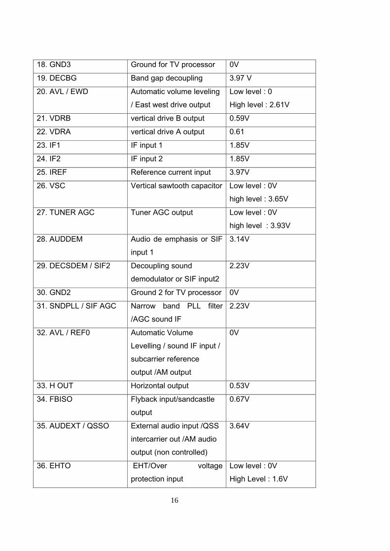
18. GND3 Ground for TV processor 0V
19. DECBG Band gap decoupling 3.97 V
20. AVL / EWD Automatic volume leveling
/ East west drive output
Low level : 0
High level : 2.61V
21. VDRB vertical drive B output 0.59V
22. VDRA vertical drive A output 0.61
23. IF1 IF input 1 1.85V
24. IF2 IF input 2 1.85V
25. IREF Reference current input 3.97V
26. VSC Vertical sawtooth capacitor Low level : 0V
high level : 3.65V
27. TUNER AGC Tuner AGC output Low level : 0V
high level : 3.93V
28. AUDDEM Audio de emphasis or SIF
input 1
3.14V
29. DECSDEM / SIF2 Decoupling sound
demodulator or SIF input2
2.23V
30. GND2 Ground 2 for TV processor 0V
31. SNDPLL / SIF AGC Narrow band PLL filter
/AGC sound IF
2.23V
32. AVL / REF0 Automatic Volume
Levelling / sound IF input /
subcarrier reference
output /AM output
0V
33. H OUT Horizontal output 0.53V
34. FBISO Flyback input/sandcastle
output
0.67V
35. AUDEXT / QSSO External audio input /QSS
intercarrier out /AM audio
output (non controlled)
3.64V
36. EHTO EHT/Over voltage
protection input
Low level : 0V
High Level : 1.6V

17
37. PLL IF IF-PLL loop filter Low level : 0V
High Level : 2.35V
38. IFVO / SVO IF video output / selected
CVBS output
3.27V
39. Vp1 Main supply voltage TV-
processor (+8 V)
8V
40. CVBSINT Internal CVBS input 2VPP
41. GND1 Ground 1 for TV-processor 0V
42. CVBS / Y External CVBS/Y input Low level : 0V
High Level : 3.3V
43. CHROMA Chrominance input
(SVHS)
Low level : 0V
High Level : 3.3V
44. AUDOUT / AMOUT Audio output /AM audio
output (volume controlled)
3.31V
45. INSSW2 2nd RGB / YUV insertion
input
0V
46. R2 / VIN 2nd R input / V (R-Y) input 2.49V
47. G2 / YIN 2nd G input / Y input 2.49V
48. B2 / UIN 2nd B input / U (B-Y) input 2.49V
49. BCLIN Beam current limiter
input/V-guard input
1.95 V
50. BLANKING Black current input 3 V
51. ROUT Red output 2Vpp
52. GOUT Green output 2Vpp
53. BOUT Blue output 2Vpp
54. VddA Analog supply of Teletext
decoder and digital supply
of TV-processor
3.3V
55. VpE OTP Programming
Voltage
0V
56. VddC Digital supply to core 3.3V
57. OSCGND Oscillator ground supply 0V

18
58. XTAL IN Crystal oscillator input 1.57V
59. XTAL OUT Crystal oscillator output 1.76V
60. RESET Reset 0V
61. VddP Digital supply to periphrery 3.3V
62. AV1 AV input from video
switching IC (+3.3 V)
0.06V
63. AV2 AV input from video
switching IC (+3.3 V) input
0.6V
64. IRIN IR Input 4.8V
11B. IC-BU4052:- 16 Pin IC. This IC is used for video switching The HEF 4052B is a dual
four channel analog Multiplexer / De- Multiplexer with common channel; select Logic. Each
Multiplexer / De-Multiplexer has four independents inputs / out puts. (Yo to Y3 ) and a
common input / out put (Z) . The Common Channel Select Logic includes two address inputs
(A0 and A1) and an active low enable input INH. Both Multiplexer / De Multiplexer has four bi
directional analog switches, each with one side connected to an independent input / out put. .
( Yo to Y3 ) and the other side connected to common input / out put ( Z). For operation as a
digital multiplexer / demultiplexer VEE is connected to VSS (typically ground).
Application Information :
• Analog Multiplexing and De-Multiplexing.
• Digital Multiplexing and demultiplexing.
• Signal Gating
PINNING: HEF 4052BP
Pin no. Pin Description Voltage in Volts ( 1 Khz Colour Pattern)
1. Y0B (independent inputs/ Out
puts)
0.50V
2. Y2B Y2/ out B (independent inputs
/ out puts)
0.50V
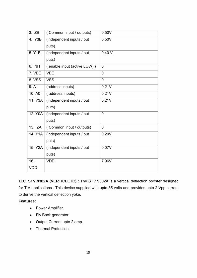
19
3. ZB ( Common input / outputs) 0.50V
4. Y3B (independent inputs / out
puts)
0.50V
5. Y1B (independent inputs / out
puts)
0.40 V
6. INH ( enable input (active LOW) ) 0
7. VEE VEE 0
8. VSS VSS 0
9. A1 (address inputs) 0.21V
10. A0 ( address inputs) 0.21V
11. Y3A (independent inputs / out
puts)
0.21V
12. Y0A (independent inputs / out
puts)
0
13. ZA ( Common input / outputs) 0
14. Y1A (independent inputs / out
puts)
0.20V
15. Y2A (independent inputs / out
puts)
0.07V
16.
VDD
VDD 7.96V
11C. STV 9302A (VERTICLE IC) : The STV 9302A is a vertical deflection booster designed
for T.V applications . This device supplied with upto 35 volts and provides upto 2 Vpp current
to derive the vertical deflection yoke. Features:
• Power Amplifier.
• Fly Back generator
• Output Current upto 2 amp.
• Thermal Protection.

20
PINNING: STV 9302
Pin no. Pin Description Voltage in Volts ( 1 Khz Colour Pattern)
1 INPUT(INVERTING) 0.59 V
2 SUPPLY VOLTAGE 14 V
3 FLY-BACK GENERATOR -11.43 V
4 Gnd or Negative supply -12.82 V
5 OUT PUT 0.33V
6 OUTPUT-STAGE SUPPLY 14.29 V
7 INPUT(NON INVERTING) 0.61 V
11D. IC-AT24C16:- This is a 16 Kilo Bite EEPROM with a wide operating range. Features:
• Data EEPROM internally organized as 2048 bytes and 128 pages X 16 bytes.
• Low power C-MOS.
• Vcc = 2.7 – 5.5 Volt operation.
• Two wire serial interface bus, I2 C- Bus Compatible.
• Filtered Inputs for Noise Suppression with Schmitt Trigger.
• Clock frequency upto 400 KHz.
• High Programming flexibility.
• High reliability
- Endurance 106 Cycles
- Data retention 40 Years.
- ESD protection 4000V on all pins.
• 8 Pin DIP/ DSO packages.
• Available for extended temperature ranges.
- Industrial -400C to + 850C
- Automotive -400C to + 1250C.
21
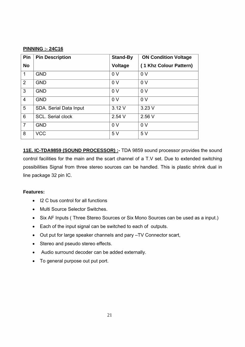
PINNING :- 24C16
Pin No
Pin Description Stand-By Voltage
ON Condition Voltage ( 1 Khz Colour Pattern)
1 GND 0 V 0 V
2 GND 0 V 0 V
3 GND 0 V 0 V
4 GND 0 V 0 V
5 SDA. Serial Data Input 3.12 V 3.23 V
6 SCL. Serial clock 2.54 V 2.56 V
7 GND 0 V 0 V
8 VCC 5 V 5 V
11E. IC-TDA9859 (SOUND PROCESSOR) :- TDA 9859 sound processor provides the sound
control facilities for the main and the scart channel of a T.V set. Due to extended switching
possibilities Signal from three stereo sources can be handled. This is plastic shrink dual in
line package 32 pin IC.
Features:
• I2 C bus control for all functions
• Multi Source Selector Switches.
• Six AF Inputs ( Three Stereo Sources or Six Mono Sources can be used as a input.)
• Each of the input signal can be switched to each of outputs.
• Out put for large speaker channels and pary –TV Connector scart,
• Stereo and pseudo stereo effects.
• Audio surround decoder can be added externally.
• To general purpose out put port.

22
PINNING: TDA 9859
Pin no. Pin Pin Description Stand By Voltage
1 AV Left input Scart Input Left
Channel
Low Level : 0.32V
High Level : 3.8V
2 P 1 Not connected Port -1 Input 0
3 MAIN Left Main Input Left
Channel
0 Low Level : 0V
High Level : 3.8V
4 CSMO Smoothing Capacitor
of reference voltage
Low Level : 0.02V
High Level : 8V
5 MAIN Right Main Input Right
Channel
Low Level : 0V
High Level : 3.8V
6 VCC Supply Voltage Low Level : 0.02V
High Level : 8V
7 AUDIO OUT Right Scart Out put right
Channel
Low Level : 0.05V
High Level : 3.8V
8 GND Ground 0
9 VO 2 Main Out put Right
Channel
Low Level : 0.17V
High Level : 3.8V
10 VI 8 Input to Loud Speaker
Channel
Low Level : 0.16V
High Level : 3.8V
11 CBR 1 Bass Capacitor
Connection-1 Right
Channel
Low Level : 0.15V
High Level : 3.8V
12 CBR 2 Bass Capacitor
Connection-2 Right
Channel
Low Level : 0.14V
High Level : 3.8V
13 Woofer out
Right( N.C)
Woofer Out Right 0
14 CTR Treble Capacitor
Connection right CH.
Low Level : 0V
High Level : 3.8V
15 MAIN OUT Right Loud Speaker Output
Right Channel
Low Level : 0V
High Level : 3.8V
23
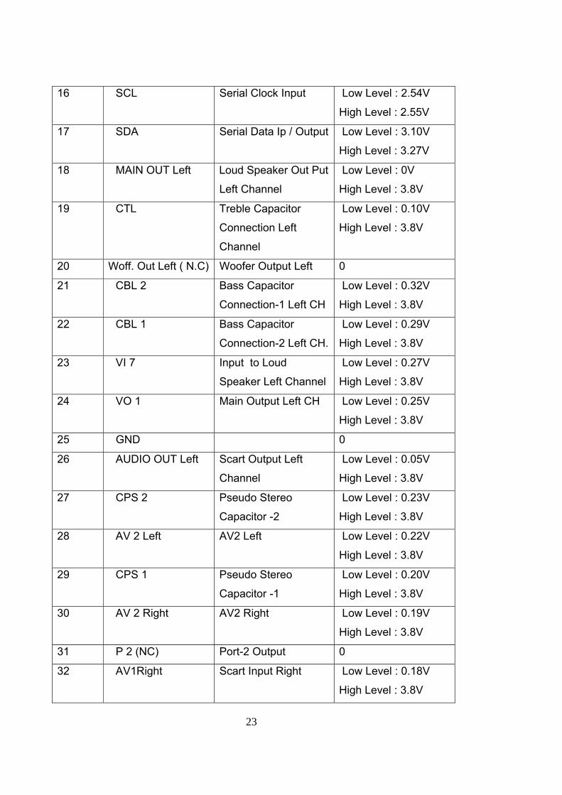
16 SCL Serial Clock Input Low Level : 2.54V
High Level : 2.55V
17 SDA Serial Data Ip / Output Low Level : 3.10V
High Level : 3.27V
18 MAIN OUT Left Loud Speaker Out Put
Left Channel
Low Level : 0V
High Level : 3.8V
19 CTL Treble Capacitor
Connection Left
Channel
Low Level : 0.10V
High Level : 3.8V
20 Woff. Out Left ( N.C) Woofer Output Left 0
21 CBL 2 Bass Capacitor
Connection-1 Left CH
Low Level : 0.32V
High Level : 3.8V
22 CBL 1 Bass Capacitor
Connection-2 Left CH.
Low Level : 0.29V
High Level : 3.8V
23 VI 7 Input to Loud
Speaker Left Channel
Low Level : 0.27V
High Level : 3.8V
24 VO 1 Main Output Left CH Low Level : 0.25V
High Level : 3.8V
25 GND 0
26 AUDIO OUT Left Scart Output Left
Channel
Low Level : 0.05V
High Level : 3.8V
27 CPS 2 Pseudo Stereo
Capacitor -2
Low Level : 0.23V
High Level : 3.8V
28 AV 2 Left AV2 Left Low Level : 0.22V
High Level : 3.8V
29 CPS 1 Pseudo Stereo
Capacitor -1
Low Level : 0.20V
High Level : 3.8V
30 AV 2 Right AV2 Right Low Level : 0.19V
High Level : 3.8V
31 P 2 (NC) Port-2 Output 0
32 AV1Right Scart Input Right Low Level : 0.18V
High Level : 3.8V
24
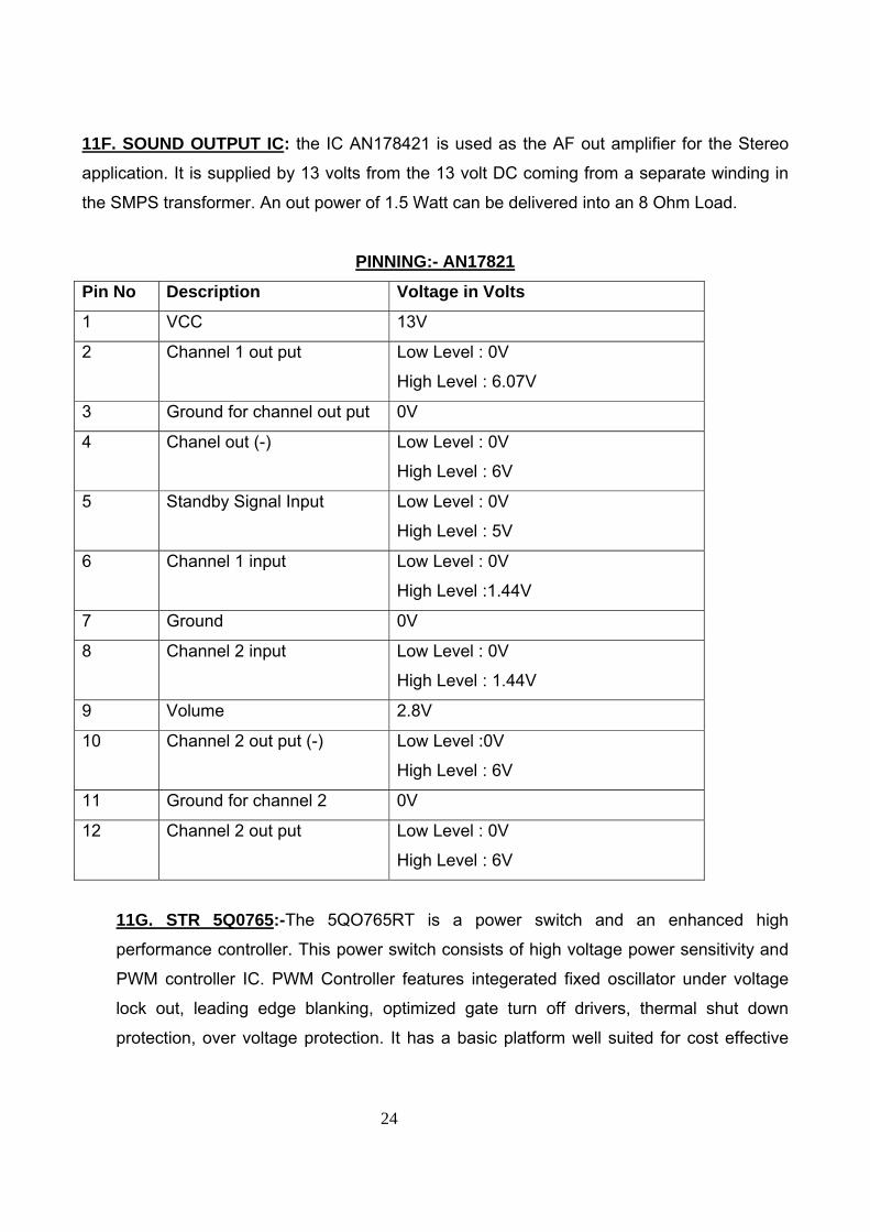
11F. SOUND OUTPUT IC: the IC AN178421 is used as the AF out amplifier for the Stereo
application. It is supplied by 13 volts from the 13 volt DC coming from a separate winding in
the SMPS transformer. An out power of 1.5 Watt can be delivered into an 8 Ohm Load.
PINNING:- AN17821
Pin No Description Voltage in Volts
1 VCC 13V
2 Channel 1 out put Low Level : 0V
High Level : 6.07V
3 Ground for channel out put 0V
4 Chanel out (-) Low Level : 0V
High Level : 6V
5 Standby Signal Input Low Level : 0V
High Level : 5V
6 Channel 1 input Low Level : 0V
High Level :1.44V
7 Ground 0V
8 Channel 2 input Low Level : 0V
High Level : 1.44V
9 Volume 2.8V
10 Channel 2 out put (-) Low Level :0V
High Level : 6V
11 Ground for channel 2 0V
12 Channel 2 out put Low Level : 0V
High Level : 6V
11G. STR 5Q0765:-The 5QO765RT is a power switch and an enhanced high
performance controller. This power switch consists of high voltage power sensitivity and
PWM controller IC. PWM Controller features integerated fixed oscillator under voltage
lock out, leading edge blanking, optimized gate turn off drivers, thermal shut down
protection, over voltage protection. It has a basic platform well suited for cost effective

25
design in CTV power supply. With this features it offers really safe and reliable power
management
Features :
• Quasi resonant convertor controller.
• Internal bus mode controller.
• Pulse by pulse current limiting.
• Over current latch protection.
• Over Voltage protection( V-Sink Min 11 Volt).
• Internal thermal Shut Down function.
• Under Voltage lock out.
• Internal High Voltage sensitivity
• Auto restart mode.
PINNING : STR 5Q0765
Pin No Description Voltage (in Volts)
1 Drain 300 V
2 Ground 0
3 VCC Low level: 12.59V
High level: 40V
4 Feedback Low level : 0.3 V
High level: 6.9V
5 SYNC Low Level : 0.74V
High Level :11V
11. VIDEO AMPLIFIER STAGE:- Transistorised amplifier circuit is used to amplify the R,G,B
signal received from TDA9351. The R,G,B output from TDA9351 is applied to base of
B911,B921 and B931 and push pull amplifier is used to amplify this signal further and applied
to cathode of CRT. Voltage details of 9 transistors used in video amplifier section are as
follows.
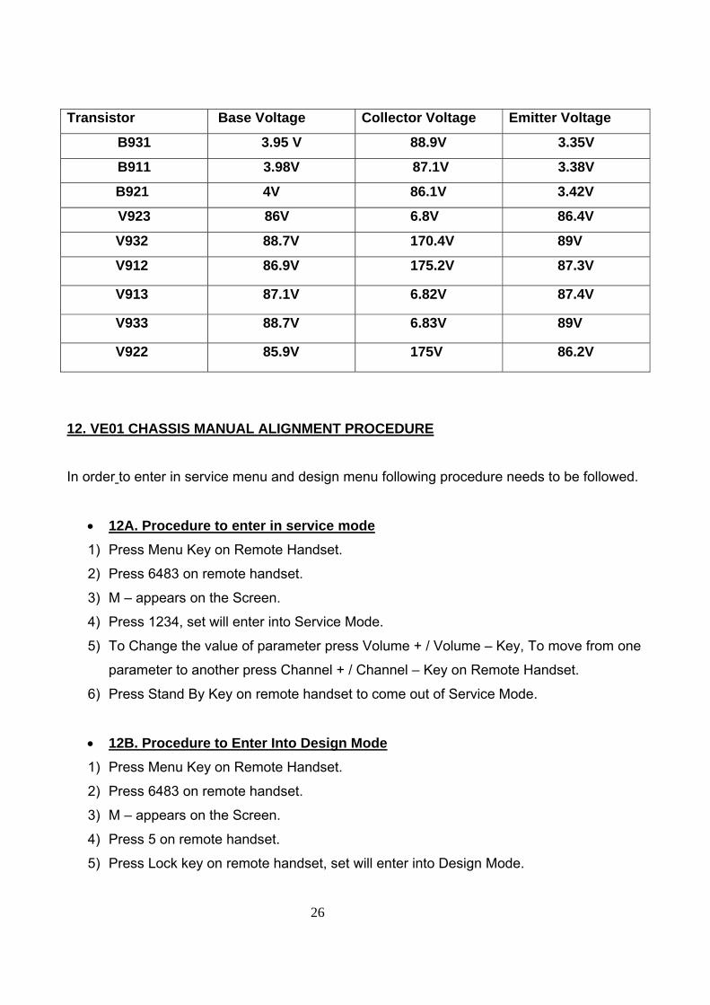
26
Transistor Base Voltage Collector Voltage Emitter Voltage
B931 3.95 V 88.9V 3.35V
B911 3.98V 87.1V 3.38V
B921 4V 86.1V 3.42V
V923 86V 6.8V 86.4V
V932 88.7V 170.4V 89V
V912 86.9V 175.2V 87.3V
V913 87.1V 6.82V 87.4V
V933 88.7V 6.83V 89V
V922 85.9V 175V 86.2V
12. VE01 CHASSIS MANUAL ALIGNMENT PROCEDURE
In order to enter in service menu and design menu following procedure needs to be followed.
• 12A. Procedure to enter in service mode 1) Press Menu Key on Remote Handset.
2) Press 6483 on remote handset.
3) M – appears on the Screen.
4) Press 1234, set will enter into Service Mode.
5) To Change the value of parameter press Volume + / Volume – Key, To move from one
parameter to another press Channel + / Channel – Key on Remote Handset.
6) Press Stand By Key on remote handset to come out of Service Mode.
• 12B. Procedure to Enter Into Design Mode 1) Press Menu Key on Remote Handset.
2) Press 6483 on remote handset.
3) M – appears on the Screen.
4) Press 5 on remote handset.
5) Press Lock key on remote handset, set will enter into Design Mode.

27
6) To Change the value of parameter press Volume + / Volume – Key, To move from one
parameter to another press Channel + / Channel – Key on Remote Handset.
7) Press “Stand-By” Key to come out of Design Mode.
• 12C. White Balance Adjustment:- ( In Field)
1) Select R,G, B cut off parameter in Menu 3 of service mode and adjust these
parameters. Standard settings of these parameters are RD=32, GD=32, BD=32
2) Select the RGB drive parameters RB, GB in menu 3 and adjust this parameter.
Default setting of these parameter is RB= 32, GB=32.
3) Select Sub brightness parameter SB in menu 3 and adjust to get proper white balance.
The default value of SB=40.
• 12D. Screen Adjustment :- (In Field)
1) Select parameter SC in menu 3 of service mode .
2) Increase the value of SC by using channel up key so that thin white line will be visible
on the screen
3) Adjust the screen intensity by varying screen pot of fbt using insulated screw driver
until a thin horizontal line is just visible.
12E. OTHER SERVICE MODE ADJUSTMENTS: - can be done by entering into service
mode by applying the suggested procedure and setting the default value mentioned below.
Few cases defaults values can be changed in a small variation for customer satisfaction.
SERVICE PRAMETERS: MENU 1
Parameter Variation Default Setting Remarks
V SLOPE 0-63 31 for 50Hz & 36 for 60Hz For adjusting picture vertical center
V SHIFT 0-63 41 for 50Hz & 36 for 60Hz For shifting picture vertical position
V SIZE 0-63 31 for 50Hz & 36 for 60Hz For adjusting Vertical amplitude
V SC 0-63 10 for 50Hz & 10 for 60Hz For adjusting Vertical S-Correction
H SHIFT 0-63 38 for 50Hz & 37 for 60Hz For adjusting picture H position
PROG NO. 1.

28
SERVICE PRAMETERS: MENU 2
Parameter Variation Default Setting Remarks
AGC 0-63 28 For RF AGC adjustment
Search Speed 0-3 0
SERVICE PRAMETERS: MENU 3
Parameter Variation Default Setting Remarks
BT 0-100 75
CT 0-100 50
SC 3 Screen variation.
RB 0-63 32 R drive.
GB 0-63 32 G Drive
RD 0-63 32 R cut off
GD 0-63 32 G cut off
BD 0-63 32 B cut off
SB 0-63 42 Sub brightness
SERVICE PRAMETERS: MENU 4
Parameter Variation Default Setting Remarks
OSD.V.POS 0-63 16 for 50Hz & 8 for 60Hz To adjust OSD Vertical position
OSD.H.POS 0-63 27 for 50Hz & 24 for 60Hz To adjust OSD horizontal position
DESIGN PRAMETERS: MENU 0
Parameter Variation Default Setting
SUB CONTRAST 0-63 63
SUB COLOR 0-63 63
SUB SHARPNESS 0-63 63
SUB TINT 0-63 31
FS-VL-H 0-255 0
FS-VL-L 0-255 0
FS-VH-H 0-255 0
FS-VH-L 0-255 0
RGB.HSH.OFFSET 0-15 6

29
DESIGN PRAMETERS: MENU 5
Parameter Variation Default Setting
PP Mode Std / dynamic / mild
Brightness 0-100 75 / 75 / 75
Contrast 0-100 75 / 100 / 50
Color 0-100 50 / 50 / 50
Sharpness 0-100 50 / 50 / 50
SC Brightness 0-63 20
Cool BD Offset 0-32 10
Warm RD Offset 0-32 10
YD PAL 0-15 8
YD NTSC 0-15 8
YD SECAM 0-15 8
YD AV PAL 0-15 8
YD AV NTSC 0-15 8
YD AV SECAM 0-15 8
DESIGN PRAMETERS: MENU 6
Parameter Variation Default Setting
OSO 0-1 1
AGC SPEED 0-3 1
FFI 0-1 0
FSL 0-1 0
FMWS 0-1 0
HP2 0-1 0
RPO 0-1 1
NTSC MATRIX JAPAN / U.S USA
VOL PIN OPEN DRAIN/ PUSH
PULL
OPEN DRAIN
VIDEO OUT IF / CVBS IF

30
DESIGN PRAMETERS: MENU 7
Parameter Variation Default Setting
IF 38.9 / 38 / 58.75/ 45.75 38.9MHZ
DK OFF / ON ON
I OFF / ON ON
BG OFF / ON ON
M OFF / ON OFF
SIF PRIORITY DK/ I/ M/ BG BG
AV2 OFF/ ON OFF
SVHS OFF/ON ON
YUV OFF/ON OFF
EURO AV OFF/ON ON
S CURVE P1 0-70 20
S CURVE V1 0-75 40
S CURVE P2 0-100 70
S CURVE V2 0-100 75
DESIGN PRAMETERS: MENU 8
Parameter Variation Default Setting
CATHOD LEVEL 0-15 4
UOC VOLUME OFF / ON OFF
FM ATT 0-63 50
TDA 9874 AVL 0-3 1
TDA 9874 CAIN 0-30 15
DUAL OUT OFF / ON OFF
AUTO SOUND OFF / ON ON
HEADPHONE 0-3 0
TRU BASS 0-1 0
DEFAULT LANG 0-17 0
LANG OPT FRENCH / RUSSIAN / RU FRENCH
LANG SW ON / OFF ON
31
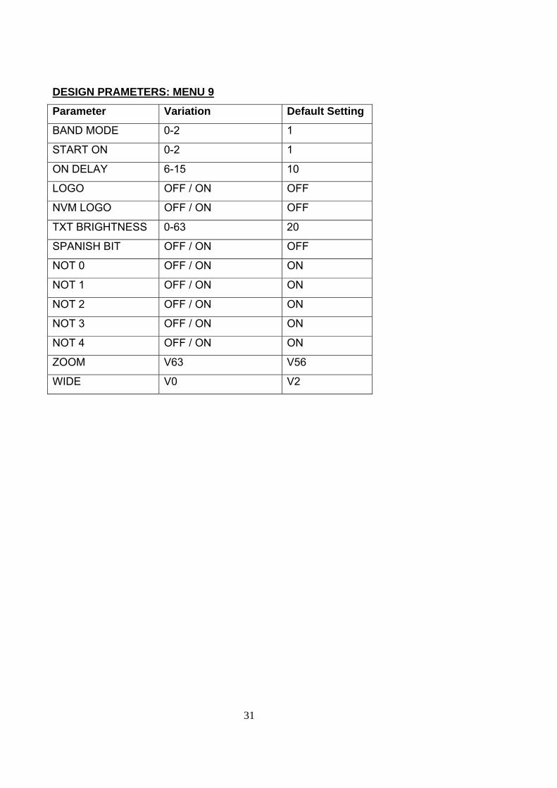
DESIGN PRAMETERS: MENU 9
Parameter Variation Default Setting
BAND MODE 0-2 1
START ON 0-2 1
ON DELAY 6-15 10
LOGO OFF / ON OFF
NVM LOGO OFF / ON OFF
TXT BRIGHTNESS 0-63 20
SPANISH BIT OFF / ON OFF
NOT 0 OFF / ON ON
NOT 1 OFF / ON ON
NOT 2 OFF / ON ON
NOT 3 OFF / ON ON
NOT 4 OFF / ON ON
ZOOM V63 V56
WIDE V0 V2

110VDC
28V
13V
8V
5V
SMPS
Micro Processor (UOC IC ) TDA 9351
FBT
Audio ProcessorTDA 9859
Tuner
Vertical outputSTV 9302A
Video Amplifier CRT
Audio OutputAN17821
Key IR
SCARTSWITCH ICHEF4052BP
FRONTAV
Memory AT24C16
HorizontalO/P TR.
HorizontalO/P driver
SpeakerBLOCK DIAGRAM
45

PRODUCT : CTV PCB/ASSY :F.A. Roadstar SHEET : 1 OF 1 RAW MATERIAL / CONSUMABLES : JIGS / FIXTURE INSTRUMENTS : PREPARED BYSR N STOCK NO LOC DESCRIPTION QPS CUTTER
1 110006308 TIE,CABLE,PLASTIC,2.5X100mm 2
1 WRAP THE SPEAKER CONNECTOR TO TIE CABLE METAL SLEEVE AT SPEAKER FITTING SCREW.2 TIE THE SPEAKER CONNECTOR TO RIGHT SIDE PORTION OF DEGAUSSING COIL SUCH THAT IT WOULD NOT
HANG OVER THE CHASSIS.3 TIE THE DEGUASSING COIL CONNECTOR TO DEGAUSSING COIL.4 CUT THE EXCESS LENGTH OF ALL THE TIES.
DO NOT LEAVE ANY CUT PORTION OF TIE ON THE CHASSIS. PRODUCT : CTV PCB/ASSY : Roadstar SHEET : 1 OF 1 RAW MATERIAL / CONSUMABLES : JIGS / FIXTURE INSTRUMENTS : PREPARED BYSR N STOCK NO LOC DESCRIPTION QPS SERVICE REMOTE
1 TV SET 11 BEFORE SWITCHING ON THE TV SET , CHECK THAT CHASSIS DOCKING AND HARNESING HAVE DONE PROPERLY OR NOT.2 CHECK THAT DEGAUSSING CONNECTOR HAS CONNECTED.3 CONNECT RF SIGNAL TO TUNER.4 SWITCH ON THE TV SET AND ADJUST THE 'SCREEN' AND 'FOCUS' POT OF FBT FOR CLEAR PICTURE.5 CHECK THAT POWER ON LED IS GLOWING WITH NORMAL INTENSITY.6 CHECK POWER ON/OFF SWITCH OPERATION BY SWITCHING THE SWITCH ON/OFF TWO TO THREE TIMES.7 CHECK FOR THE PROBLEMS LIKE CPT GAP, SWITCH OFF SPOT, STRAY EMISSION ,ETC.8 SELECT CHANNEL "EU 2CH" AND CHECK THAT 'SUB BRIGHTNESS' PATTERN HAS APPEARED .9 CHECK FOR CHANNEL TUNNING, ELSE TUNE THE PROGRAMS USING "AUTO SEARCH" IN SEARCH MENU.10 CHECK THE VOLUME VARIATION FROM ZERO TO MAXIMUM. OBSERVE THAT VARIATION IS NOT INTERMITANT. IT SHOULD BE 11 CHECK THE OPERATION OF CH UP/ CH DN/ VOL UP/ VOL DN/ MENU KEYS .12 CHECK THAT THESE KEYS ARE NOT HARD TO OPERATE.13 CHECK THE TV SET ASTHETICALLY
PRODUCT : CTV PCB/ASSY :F.A. Roadstar SHEET : 1 OF 1 RAW MATERIAL / CONSUMABLES : JIGS / FIXTURE INSTRUMENTS : PREPARED BYSR N STOCK NO LOC DESCRIPTION QPS DIGITAL PANEL METER
1 TV SET 1 ALIGNER2 REMOTE CHECKED BY1 SWITCH ON THE SET.2 CONNECT THE RF CORD TO TUNER.3 SELECT THE 'STANDARD' MODE OF PICTURE CONTROL.4 CONNECT THE DPM POSITIVE PROBE TO CATHODE OF DIODE "VD631" .
( DPM NEGATIVE PROBE IS INTERNALLY CONNECTED TO CHASSIS GROUND)5 ROTATE THE PRESET "VR 631" USING ALIGNER TO SET +B VOLTAGE + 115V +/- 0.5V DC
VE01 CHASSIS ALLIGNMENT PROCEDURE ON MANUFACTURING LINE
STAGE: HARNESING AT F-A LINE
STAGE: SWITCH ON
STAGE: +B VOLTAGE ALIGNMENT
1

PRODUCT : CTV PCB/ASSY :FA Roadstar SHEET : 1 OF 1 RAW MATERIAL / CONSUMABLES : JIGS / FIXTURE INSTRUMENTS : PREPARED BYSR N STOCK NO LOC DESCRIPTION QPS SERVICE REMOTE
1 TV SET 1 FEVIBONAD2 INSULATED SCREW CHECKED BY3 DRIVER
NOTE : WARM UP THE TV SET FOR AT LEAST 20 MINUTES ( DURING SOAKING AREA)1 SELECT DIGITAL / RETMA / LION HEAD PATTERN , 2 PRESS "MENU+6483" KEYS SEQUENCE TO ACCESS THE MANUFACTURING MODE.3 PRESS KEY '3' TO APPEAR 'SERVICE MENU 3' ON SCREEN. 4 SELECT PARAMETER "SC " BY PRESSING CHANNEL UP/DN KEY .5 PRESS 'VOL UP' KEY THEN A THIN HORIZONTAL LINE WILL BE DISPLAYED ON SCREEN.6 ADJUST THE SCREEN INTENSITY BY VARYING SCREEN POT OF FBT USING INSULATED SCREW DRIVER UNTIL A THIN HORIZON
LINE IS JUST VISIBLE.7 PRESS "VOL DN" KEY TO APPEAR ORIGINAL PATTERN.8 APPLY THE FEVIBOND ON "SCREEN" POT. OF FBT.
PRODUCT : CTV STAGE: FOCUS AND CONVERGENCE PCB/ASSY : F.A. Roadstar SHEET : 1 OF 1 RAW MATERIAL / CONSUMABLES : JIGS / FIXTURE INSTRUMENTS : PREPARED BYSR N STOCK NO LOC DESCRIPTION QPS SERVICE REMOTE
1 TV SET 1 GLUE2 PNUE. SCREW DRIVER CHECKED BY3
FEVIBONADINSULATED SCREW APPROVED BYDRIVER
TIGHTENING TORQUE OF SCREW DRIVER- 10 TO 15 kg.cm and TV SET IS FACING TOWARDS EAST.FOCUS ADJUSTMENT :-
1 SELECT LION HEAD PATTERN.( EU 5CH) . CHOOSE SELECTABLE PICTURE MODE "STANDARD".2 ADJUST THE FOCUS KNOB ON FBT USING INSULATED SCREW DRIVER , SO THAT '30' AT THE DIAGONAL CENTRE ON LION HEA
WILL GET AS SHARP AS POSSIBLE. THIS SYMBOL INDICATES THE LOCATION OF FOCUS ADJUSTMENT CHECK ON SCREEN.
CONVERGENCE ADJUSTMENT :-1 SWITCH OVER TO CROSS HATCH PATTERN.2 BY TURNING THE 4 POLE MAGNET, MATCH THE RED AND BLUE LINES AT THE CENTRE. SHIFT THE RED AND BLUE LINE
OVER THE GREEN LINE BY USING 6 POLE MAGNET.3 TIGHTEN THE CPM LOCK. BE CAREFUL NOT TO MOVE THE OTHER RINGS/MAGNETS AT THIS TIME.4 CHECK AND ADJUST THE PICTURE FOR TILT.ADJUST THE TILT BY ADJUSTING THE YOKE.5 APPLY GLUE ON BOTH SCREEN AND FOCUS KNOB OF FBT AFTER ADJUSTMENT OF FOCUS.
FOR TFT CPT MODELS: TILT=0 mm TILT CHECKFOR CONVENTIONAL CPT MODELS: TILT=2 mm FOCUS CHECKNOTE: DO NOT TOUCH TO ANY PART OF FBT.
PRODUCT : CTV STAGE: CONVERGENCE PCB/ASSY : F.A. Roadstar SHEET : 1 OF 2 RAW MATERIAL / CONSUMABLES : JIGS / FIXTURE INSTRUMENTS : PREPARED BYSR N STOCK NO LOC DESCRIPTION QPS SERVICE REMOTE
1 TV SET
STAGE: SCREEN ADJUSTMENT
CONVERGENCE ADJUSTMENTSNOTE : Before attempting any convergence adjustments, the receiver should be operated for at leat fifteen minutes.
CENTER CONVERGENCE ADJUSTMENT :1.Select the Cross-hatch pattern (EU 4CH) .2.Set the brightness and contrast for well defined pattern.3. Adjust two tabs of the 4-Pole magnets to change the angle between them . ( See fig.-01 & 02) and superimpose red and blue vertical lines in the center area of picture screen.4.Turn the both tabs at the same time keeping the angle constant to superimpose red and blue horizontal lines at the center of the screen. (See fig-04 & 02)5.Adjust two tabs of 6-Pole magnets to superimpose red/blue line and green one .Adjusting the angle affects the vertical lines and rotating both magnets affects the horizontal lines.6.Repeat adjustments 3,4,5 keeping in mind red, green and blue movement , because 4-Pole Magnets and 6-Pole Magnets have mutual interaction and make line movement complex
CIRCUMFERENCE CONVERGENCE ADJUSTMENT:1. Loosen the clamping screw of deflection yoke slightly to allow the yoke to tilt.2.Temporarily put a wedge as shown in fig1. ( Do not remove cover paper on adhesive part of the wedge.)3.Tilt front of the deflection yoke up or down to obtain better convergence in circumference (see fig.3). Push the mounted wedge in to the space between picture tube and the yoke, to fix the yoke temporarily.4.Put other wedge in to bottom space and remove the cover paper to stick.5.Tilt front of the yoke right or left to obtain better convergence in circumference. (see fig.3)6.Keep the yoke position and put another wedge in either upper space. Remove cover paper and stick the wedge on picture tube to fix the yoke.7.Detach the temporarily mounted wedge and put it in another upper space.Stick it on picture tube to fix the yoke.8.After fixing three wedges , recheck overall convergence. Tighten the screw firmly to fix the yoke and check the yoke is firm.9.stick three adhesive tapes on wedges as shown in fig.o.
THIS HORIZONTAL LINE MATCHING WITH EXPOSURE POINTS
EXPOSURE POINTSON THE SCREEN
EXPOSURE POINTS ON THE SCREEN
THIS HORIZONTAL LINE MATCHING WITH EXPOSURE POINTS
2
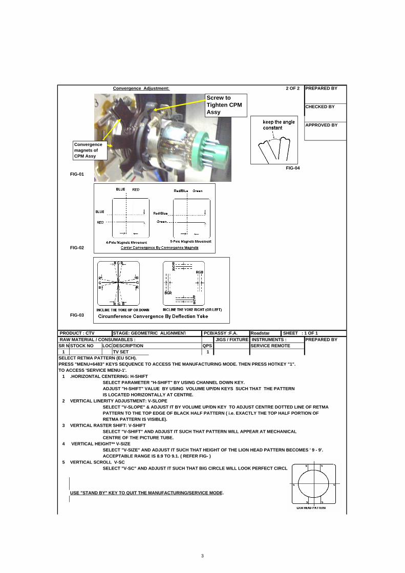
Convergence Adjustment: 2 OF 2 PREPARED BY
CHECKED BY
APPROVED BY
FIG-04FIG-01
FIG-02
FIG-03
PRODUCT : CTV PCB/ASSY :F.A. Roadstar SHEET : 1 OF 1 RAW MATERIAL / CONSUMABLES : JIGS / FIXTURE INSTRUMENTS : PREPARED BYSR N STOCK NO LOC DESCRIPTION QPS SERVICE REMOTE
1 TV SET 1SELECT RETMA PATTERN (EU 5CH).PRESS "MENU+6483" KEYS SEQUENCE TO ACCESS THE MANUFACTURING MODE. THEN PRESS HOTKEY "1".TO ACCESS 'SERVICE MENU-1'.
1 .HORIZONTAL CENTERING: H-SHIFTSELECT PARAMETER "H-SHIFT" BY USING CHANNEL DOWN KEY.ADJUST "H-SHIFT" VALUE BY USING VOLUME UP/DN KEYS SUCH THAT THE PATTERN IS LOCATED HORIZONTALLY AT CENTRE.
2 VERTICAL LINERITY ADJUSTMENT: V-SLOPESELECT "V-SLOPE" & ADJUST IT BY VOLUME UP/DN KEY TO ADJUST CENTRE DOTTED LINE OF RETMAPATTERN TO THE TOP EDGE OF BLACK HALF PATTERN ( i.e. EXACTLY THE TOP HALF PORTION OF RETMA PATTERN IS VISIBLE).
3 VERTICAL RASTER SHIFT: V-SHIFTSELECT "V-SHIFT" AND ADJUST IT SUCH THAT PATTERN WILL APPEAR AT MECHANICAL CENTRE OF THE PICTURE TUBE.
4 VERTICAL HEIGHT** V-SIZESELECT "V-SIZE" AND ADJUST IT SUCH THAT HEIGHT OF THE LION HEAD PATTERN BECOMES ' 9 - 9'.ACCEPTABLE RANGE IS 8.9 TO 9.1. ( REFER FIG- )
5 VERTICAL SCROLL V-SCSELECT "V-SC" AND ADJUST IT SUCH THAT BIG CIRCLE WILL LOOK PERFECT CIRCLE.
USE "STAND BY" KEY TO QUIT THE MANUFACTURING/SERVICE MODE.
STAGE: GEOMETRIC ALIGNMENT
Screw to Tighten CPM Assy
Convergence magnets of CPM Assy
3

PRODUCT : CTV PCB/ASSY :F.A. Roadstar SHEET : 1 OF 1 RAW MATERIAL / CONSUMABLES : JIGS / FIXTURE INSTRUMENTS : PREPARED BYSR N STOCK NO LOC DESCRIPTION QPS SERVICE REMOTE
1 TV SET 1PRESS "MENU+6483" KEYS SEQUENCE TO ACCESS THE MANUFACTURING MODE. THEN PRESS HOTKEY "1".SELECT RETMA PATTERN (EU 5CH).OSD DISPLAY ADJUSTMENT ** VERTICAL AND HORIZONTAL *** OSDH AND OSDV
SELECT SERVICE MENU -4 BY PRESSING HOTKEY "4"..A BIG RECTANGLE WILL APPEAR ON SCREEN.
1 SELECT "OSD V-POS" BY CH.DN KEY. AND ADJUST DOTTED RECTANGLE AT THE VERTICAL CENTRE OF SCREEN.2 SELECT "OSD H-POS" BY CH.DN KEY. AND ADJUST DOTTED RECTANGLE AT THE HORIZONTAL CENTRE OF SCREEN.
USE "STAND BY" KEY TO QUIT THE MANUFACTURING/SERVICE MODE.
OSD ALIGNMENT ON NTSC PATTERN:2 SELECT COLOUR BAR+CIRCLE PATTERN ( NTSC SYSTEM )
SELECT PARAMETER "OSD V-POS " & "OSD H-POS" BY CHANNEL UP/ DN KEYS . ADJUST THE PARAMETER VALUES SUCH THAT A BIG DOTTED RECTANGLE SHOULD BE SYMMETRICALLY LOCATED ON RETMA PATTERN.
PRODUCT : CTV PCB/ASSY : F.A. CHASSIS : ALL SHEET : 1 OF 1 RAW MATERIAL / CONSUMABLES : JIGS / FIXTURE INSTRUMENTS : PREPARED BYSR N STOCK NO LOC DESCRIPTION QPS SERVICE REMOTE
1 TV SET 1INTRODUCTION TO WHITE BALANCE ADJUSTMENT WINDOW
STAGE: WHITE BALANCE ADJUSTMENT
WHITE BALANCE
STAGE: OSD ALIGNMENT
THIS INDICATES WHITBALANCE CONDITION "NG" OR "GOOD"
TARGET VALUES OF WHITE BALANCE
TOLERANCE OF TARGET VALUES
GREEN AND BLUE DRIVE STATUS BARS
GREEN AND BLUE CUT OFF STATUS BARS
SUB CONTRAST STATUS BAR
SUB BRIGHTNESS STATUS BAR
CURRENT STATUS
MODEL SELECTION WINDOW
4

PRODUCT : CTV PCB/ASSY : F.A. Roadstar SHEET : 2 OF 2 RAW MATERIAL / CONSUMABLES : JIGS / FIXTURE INSTRUMENTS : PREPARED BYSR N STOCK NO LOC DESCRIPTION QPS SERVICE REMOTE
1 TV SET 1NOTE : WARM UP THE TV SET FOR AT LEAST 20 MINUTES ( DURING SOAKING AREA)ENSURE "TONE" IN SETTINGS MENU IS "NORMAL" AND SELECTABLE PICTURE MODE IS "STANDARD"..
1 ENSURE THAT THE MODEL NAME DISPLAYED IN 'MODEL INFORMATION WINDOW' IS CORRECT.2 TV SET WILL STOP IN FRONT OF CAMERA SENSOR ,CONNECT WHITE BALANCE SIGNAL FROM WHITE BALANCE TESTER.
TO TUNER INPUT OF SET.3 AUTO DEGAUSSING WILL START.OBSERVE THAT , WHILE DEGAUSSING ,MONITOR DISPLAY WILL
APPEAR VIBRATING.AFTER DEGAUSSING , SENSOR WILL COME FORWARD TILL IT JUST TOUCHES TO SCREEN.4 ENSURE THAT THE SET POSITION IS SUCH THAT SCREEN WILL BE IN FRONT OF SENSOR.AS WELL AS NEAR TO IT.
TAKE CARE THAT NO OSD WILL BE IN FRONT OF SENSOR SO THAT IT WILL NOT GET SENSED BY SENSOR WHILE TESTING AND ADJUSTMENT OF WHITE BALANCE.
5 PRESS "MENU+6483" KEY AND HOTKEY "3" , SELECT SERVICE PARAMETERS FOR RGB CUTOFF 7 ADJUSTMENT & ADJUST IT BY VOL. UP/ VOL. DN KEYS. IF NEEDED ADJUST THE VALUES FOR PARAMETERS OF RGB DRIVES6 IF NECESSARY, ADJUST THE 'SUB BRIGHTNESS' VALUE BY SELECTING APPROPREATE SERVICE PARAMETER.7 THE ADJUSTMENTS ARE MUTUALLY INTERDEPENDENT SO ADJUST ALL ABOVE MENTIONED PARAMETERS TILL THE RED BLO
BAR COMES AT CENTRE AND "NG" DISPLAY TURNS IN TO "GOOD" .SERVICE PARAMETERS:- SPECIFICATIONS:
RGB CUTOFF'S FOR ALL OTHER BRANDSUOC/VX05T/ PIPMOC POC/ROADSTAR TSB2 VX04T X= 275+/- 5RDC RD RD R CUT RDC y= 292+/- 5GDC GD GD G CUT GDC FOR LOW BEAM Y=15BDC BD BD B CUT BDC FOR HIGH BEAM Y=113 RGB DRIVESGDRV GB GB GDRV GDRV FOR TOSHIBA BRANDBDRV RB RB BDRV BDRV X= 260 SUB BRIGHTNESS y= 271SBRT SBRT SUB-BRI BRTS BRTC FOR LOW BEAM Y= 5USE "STAND BY" KEY TO QUIT THE MANUFACTURING/SERVICE MODE FOR HIGH BEAM Y= 99
PRODUCT : CTV STAGE: SOUND Q.C.-1 PCB/ASSY :F.A. Roadstar SHEET : 1 OF 1 RAW MATERIAL / CONSUMABLES : JIGS / FIXTURE INSTRUMENTS : PREPARED BYSR N STOCK NO LOC DESCRIPTION QPS REMOTE
1 TV SET 11 CONNECT THE RF SIGNAL CORD TO TUNER. 2 CHECK FOR VOLUME VARIATION FROM ZERO TO MAX. (FOR CH-02 & CH-05) SOUND SHOULD BE DISTORTION
FREE AT MAX. VOLUME LEVEL.3 CHECK FOR HISSING SOUND , DISTORTED SOUND PROBLEMS.. 4 CHECK SOUND MUTE, AVL.5 BANG THE CHASSIS FOR LOOSE CONTACT .6 REMOVE THE RF SIGNAL CORD FROM TUNER.7 FOR DETAILS, PLEASE REFER USERS GUIDE BOOK
PRODUCT : CTV STAGE: PICTURE Q.C.-1 PCB/ASSY :F.A. Roadstar SHEET : 1 OF 1 RAW MATERIAL / CONSUMABLES : JIGS / FIXTURE INSTRUMENTS : PREPARED BYSR N STOCK NO LOC DESCRIPTION QPS
1 TV SET 1 SERVICE REMOTE2 EXT. DEGAUSSING COIL CHECKED BY1 CONNECT RF SIGNAL CORD TO TUNER .2 SELECT CHANNEL "EU 5CH" .CHECK FOR GEOMETRICAL ALIGNMENTS, DISPLAY ALIGNMENTS,(HEIGHT & WIDTH SHOULD BE
HEAD PATTERN.) LION HEAD PATTERN SHOULD LOOK LINEAR AND SYMMETRICAL .
3 CHECK FOR FOCUS ADJUSTMENT AT DIAGONAL CENTRE OF PICTURE TUBE. '30' DIGITS ON LION HEAD PATTERN SHOULD BE SHARP VISIBLE.
4 PRESS "ZOOM' KEY ON REMOTE TO SELECT "ZOOM' MODE AND CHECK THAT HEIGHT OF THE RETMA PATTERN IS SELECT "WIDE" MODE AND CHECK THAT PATTERN HEIGHT IS 75% OF THE SCREEN.
5 SELECT CROSS HATCH PATTERN (EU 4CH) AND CHECK FOR CONVERGENCE QUALITY. HORIZONTAL AND VERTICAL LINES SHOULD BE WHITE.
6 CHECK FOR SUB BRIGHTNESS ON CHANNEL ( EU 2CH).. SUB BRIGHTNESS SHOULD BE SUCH THAT 5 & 1/2 BARS ON SUB BRIGHTNESS PATTERN WITH PICTURE MODE "STANDARD" ARE VISIBLE .IF REQUIRED ADJUST PARAMETER "SB" IN SERVICE MENU-HOTKEY-3 FOR SPECIFIED SUB BRIGHTNESS ALIGNMENT.
7 CHECK THAT OSD DISPLAY IS NOT CUTTING ON COLOUR BAR+CIRCLE PATTERN WHEN 'ZOOM' MODE IS SELECTED.8 CHECK FOR P-CONTROL- CONTRAST,BRIGHTNESS,COLOUR ,SHARPNESS.9 CHECK FOR ALL BANDS TUNING WITH THEIR RESPECTIVE SOUND.10 CHECK FOR WHITE BALANCE, TILT ALIGNMENT.& COLOUR PATCH. 11 CHECK FOR SELECTABLE PICTURE MODES AS STANDARD,DYNAMIC, MILD , USER. 12 CHECK CPT RELATED PROBLEMS (SCRATCH/CONVERGENCE-DYNAMIC&STATIC / YOKE TILT,CPT GAP OR TILT).13 CHECK FOR RASTER COLLAPSE DURING SWITCH OFF, CHECK FOR THE PROBLEMS SUCH AS DAMPING
BAR, BLOOMING, RETRACE LINES, STRAY EMISSION ETC.14 FOR DETAILS, PLEASE REFER USERS GUIDE BOOK
USE "STAND BY" KEY TO QUIT THE MANUFACTURING/SERVICE MODE
STAGE: WHITE BALANCE ADJUSTMENT
WHITE BALANCE METER
SB
WGWB
DSPM2129CRCGCB
5

PRODUCT : CTV STAGE: TELETEXT CHECKING PCB/ASSY :F.A. CHASSIS :ROA SHEET : 1 OF 1 RAW MATERIAL / CONSUMABLES : JIGS / FIXTURE INSTRUMENTS : PREPARED BYSR N STOCK NO LOC DESCRIPTION QPS
1 TV SET 1 REMOTETELETEXT CHECKING: SELECT COLOUR BAR PATTERN. PRESS "TXT/MIX" KEY ON REMOTE
1 OBSERVE THAT "P100 (INDEX PAGE OF TELETEXT) HAS APPEARED. PRESS "TXT/MIX" KEY AGAIN AND OBSERVE THAT THE TE2 PAGE HAS SUPERIMPOSED ON THE COLOUR BAR PATTERN. SELECT PAGE "P102" BY USING PROGRAM UP KEY AND OBSERV3 THAT " *** LARGE CHARACTERS *** " PAGE HAS APPEARED. . PRESS "TV/AV" KEY TO QUIT FROM TELETEXT MODE.
4 SELECT SETTINGS MENU AND CHECK THAT TXT=EAST/WEST " FUNCTION.5 PRESS "SUB CODE " KEY ON REMOTE & CHECK "DK/I/BG" OPTIONS
PRODUCT : CTV STAGE: NTSC / H.V. CHECKING PCB/ASSY :F.A. Roadstar SHEET : 1 OF 1 RAW MATERIAL / CONSUMABLES : JIGS / FIXTURE INSTRUMENTS : PREPARED BYSR N STOCK NO LOC DESCRIPTION QPS
1 TV SET 1 REMOTE2 HV METER CHECKED BY3 HAND GLOVES4 BALUN
NTSC CHECK:1 SELECT COLOUR BAR+CIRCLE PATTERN.2 SELECT COLOUR SYSTEM=NTSC IN 'SETTINGS ' MENU.3 SELECT TINT OPTION IN PICTURE MENU. AND VARY ITS VALUE .4 WHILE TINT VARIATION ,CHECK THAT RED COLOUR IS CHANGING.5 IF FOUND ANY ABNORMALITY IN CHECKING , PLEASE REJECT THE SET.
H.V. TEST1 REMOVE THE MAINS CORD FROM PALLET AND INSERT IT IN HV SOCKET.(SPECIALLY PROVIDED)2 SNAP SPECIAL BALUN INTO TUNER POINT.3 TOUCH THE HV TERMINAL TO BALUN POINT.4 PRESS THE TEST /ENABLE BUTTON ON HV TESTER,IF BUZZER OPERATES FOR UNSPECIFIED TIME THEN REJECT THE SET.5 REMOVE MAINS CORD FROM SOCKET AND INSERT IN PALLET SOCKET.6 RELEASE THE SET FOR NEXT STAGE.
AFTER CHECKING, MAKE "M-MODE" ON BY PRESSING "SERVICE KEY+DEMO KEY".SETTING PARAMETER: 1.1KV, 3mA, FOR 3 SEC.
PRODUCT : CTV STAGE: NTSC ALIGNMENTS PCB/ASSY :F.A. Roadstar SHEET : 1 OF 1 RAW MATERIAL / CONSUMABLES : JIGS / FIXTURE INSTRUMENTS : PREPARED BYSR N STOCK NO LOC DESCRIPTION QPS NTSC PATTERN
1 TV SET 1 GENERATOR3 SERVICE REMOTE 4 FOR NTSC ALIGNMENTS1 SELECT NTSC PATTERN .( COLOR BAR+CIRCLE PATTERN )2 PRESS "MENU+6483" KEYS SEQUENCE TO ACCESS THE MANUFACTURING MODE. THEN PRESS HOTKEY "1" TO ENABLE MENU-1.1 .HORIZONTAL CENTERING: H-SHIFT
SELECT PARAMETER "H-SHIFT" BY USING CHANNEL DOWN KEY.ADJUST "H-SHIFT" VALUE BY USING VOLUME UP/DN KEYS SUCH THAT THE PATTERN IS LOCATED HORIZONTALLY AT CENTRE.
2 VERTICAL LINERITY ADJUSTMENT: V-SLOPESELECT "V-SLOPE" & ADJUST IT BY VOLUME UP/DN KEY SUCH THAT EXACTLY THE TOP HALF PORTION OFRETMA PATTERN IS VISIBLE.
3 VERTICAL RASTER SHIFT: V-SHIFTSELECT "V-SHIFT" AND ADJUST IT SUCH THAT PATTERN WILL APPEAR AT MECHANICAL CENTRE OF THE PICTURE TUBE.
4 VERTICAL HEIGHT** V-SIZESELECT "V-SIZE" AND ADJUST IT SUCH THAT HEIGHT OF THE LION HEAD PATTERN BECOMES ' 9 - 9'.ACCEPTABLE RANGE IS 8.9 TO 9.1. ( REFER FIG- )
5 VERTICAL SCROLL V-SCSELECT "V-SC" AND ADJUST IT SUCH THAT BIG CIRCLE WILL LOOK PERFECT CIRCLE
PRODUCT : CTV STAGE: AV CHECKING PCB/ASSY :F.A. Road Star SHEET : 1 OF 1 RAW MATERIAL / CONSUMABLES : JIGS / FIXTURE INSTRUMENTS : PREPARED BYSR N STOCK NO LOC DESCRIPTION QPS REMOTE H-SET
1 TV SET 1 MONITOR av out SET2 AV CORDS CHECKED BY3 monitor av in tv set
CONNECT THE RF SIGNAL CORD TO TUNNER. SELECT CHANNEL "EU 2CH".AV IN CHECKING -
1 KEEP MONITOR SET IN TV MODE AND 'TESTING TV SET' IN 'EURO AV' MODE BY USING "TV/AV" KEY ON REMOTE.2 CHANNEL "EU 2CH" IS SELECTED IN MONITOR TV SET.3 CONNECT "VIDEO OUT" AND "AUDIO OUT" CORD OF MONITOR SET TO "VIDEO IN " AND "AUDIO IN" JACKS OF TESTING TV SET 4 LISTEN FOR NORMAL SOUND AND PICTURE OF CHANNEL "EU 2CH" PRESENT IN THE "TESTING TV SET" .5 CHECK THE AUDIO FOR BOTH THE AUDIO IN JACKS.
AV OUT CHECKING:- 1 KEEP MONITOR SET IN 'AV' MODE AND 'TESTING TV SET' IN 'TV' MODE BY USING "TV/AV" KEY ON REMOTE.2 SELECT SUB BRIGHTNESS PATTERN (EU 2CH) ON TESTING TV SET.3 CONNECT "VIDEO IN" AND "AUDIO IN" CORD OF MONITOR SET TO "VIDEO OUT " AND "AUDIO OUT" JACKS OF TESTING TV SET 4 LISTEN FOR NORMAL SOUND AND PICTURE OF CHANNEL "EU 2CH" PRESENT IN THE "MONITOR TV SET" .5 REMOVE THE AV CORDS AFTER TESTING.
CHECK "CD PLAY=ON/OFF" FUNCTION IN SOUND MENU
6
PRODUCT : CTV STAGE: SOUND Q.C.-2 PCB/ASSY :F.A. RoadStar SHEET : 1 OF 1 RAW MATERIAL / CONSUMABLES : JIGS / FIXTURE INSTRUMENTS : PREPARED BYSR N STOCK NO LOC DESCRIPTION QPS
1 TV SET 1 REMOTE2 HAMMER CHECKED BY1 CONNECT THE RF SIGNAL CORD TO TUNER. 2 CHECK FOR VOLUME VARIATION FROM ZERO TO MAX. (FOR CH-02 & CH-05) SOUND SHOULD BE DISTORTION
FREE AT MAX. VOLUME LEVEL.3 CHECK FOR HISSING SOUND , DISTORTED SOUND PROBLEMS.. 4 CHECK SOUND MUTE, AVL.5 BANG THE CHASSIS FOR LOOSE CONTACT .6 REMOVE THE RF SIGNAL CORD FROM TUNER.7 FOR DETAILS, PLEASE REFER USERS GUIDE BOOK.
SHOCK TEST:1 GENTLY HIT THE HAMMER ON TOP SIDE OF FRONT COVER. CHECK FOR ANY ABNORMALITY
PRODUCT : CTV STAGE: PICTURE Q.C.-2 PCB/ASSY :F.A. RoadStar SHEET : 1 OF 1 RAW MATERIAL / CONSUMABLES : JIGS / FIXTURE INSTRUMENTS : PREPARED BYSR N STOCK NO LOC DESCRIPTION QPS
1 TV SET 1 SERVICE REMOTE 1 CONNECT RF SIGNAL CORD TO TUNER .2 SELECT CHANNEL "EU 5CH" .CHECK FOR GEOMETRICAL ALIGNMENTS, DISPLAY ALIGNMENTS,(HEIGHT & WIDTH SHOULD BE
HEAD PATTERN.) LION HEAD PATTERN SHOULD LOOK LINEAR AND SYMMETRICAL .
3 CHECK FOR FOCUS ADJUSTMENT AT DIAGONAL CENTRE OF PICTURE TUBE. '30' DIGITS ON LION HEAD PATTERN SHOULD BE SHARP VISIBLE.
4 PRESS "ZOOM' KEY ON REMOTE TO SELECT "ZOOM' MODE AND CHECK THAT HEIGHT OF THE RETMA PATTERN IS SELECT "WIDE" MODE AND CHECK THAT PATTERN HEIGHT IS 75% OF THE SCREEN.
5 SELECT CROSS HATCH PATTERN (EU 4CH) AND CHECK FOR CONVERGENCE QUALITY. HORIZONTAL AND VERTICAL LINES SHOULD BE WHITE.
6 CHECK FOR SUB BRIGHTNESS ON CHANNEL ( EU 2CH).. SUB BRIGHTNESS SHOULD BE SUCH THAT 5 & 1/2 BARS ON SUB BRIGHTNESS PATTERN WITH PICTURE MODE "STANDARD" ARE VISIBLE .IF REQUIRED ADJUST PARAMETER "SBI" IN SERVICE MENU-HOTKEY-3 FOR SPECIFIED SUB BRIGHTNESS ALIGNMENT.
7 CHECK THAT OSD DISPLAY IS NOT CUTTING ON COLOUR BAR+CIRCLE PATTERN WHEN 'ZOOM' MODE IS SELECTED.8 CHECK FOR P-CONTROL- CONTRAST,BRIGHTNESS,COLOUR ,SHARPNESS.9 CHECK FOR ALL BANDS TUNING WITH THEIR RESPECTIVE SOUND.10 CHECK FOR WHITE BALANCE, TILT ALIGNMENT.& COLOUR PATCH. 11 CHECK FOR SELECTABLE PICTURE MODES AS STANDARD,DYNAMIC, MILD , USER. 13 CHECK CPT RELATED PROBLEMS (SCRATCH/CONVERGENCE-DYNAMIC&STATIC / YOKE TILT,CPT GAP OR TILT).14 CHECK FOR RASTER COLLAPSE DURING SWITCH OFF, CHECK FOR THE PROBLEMS SUCH AS DAMPING
BAR, BLOOMING, RETRACE LINES, STRAY EMISSION ETC.15 FOR DETAILS, PLEASE REFER USERS GUIDE BOOK
PRODUCT : CTV STAGE: FEATURE CHECKING PCB/ASSY :F.A. RoadStar SHEET : 1 OF 1 RAW MATERIAL / CONSUMABLES : JIGS / FIXTURE INSTRUMENTS : PREPARED BYSR N STOCK NO LOC DESCRIPTION QPS
1 TV SET 1 REMOTESWITCH ON THE SET.SELECT FOLLOWING FUNCTIONS -
1 SELECT "SETTINGS" MENU AND CHECK 'EURO AV' FOR 'Y/C, RGB, VIDEO' OPTIONS.2 IN SETTINGS MENU - CHECK TONE=NORMAL, WARM, COOL.3 CHECK 'BLACK STRETCH' IN SETTINGS MENU-BRIGHTNESS INCREASES WHEN BLACK STRETCH IS 'OFF'.4 SELECT "TIMER" MENU AND CHECK THAT ON TIMER, OFF TIMER, REPEAT SETTINGS ARE AVAILABLE.5 SELECT "SETTINGS--->LANGUAGE" MENU AND CHECK THAT 18 DIFFERENT LANGUAGES ARE AVAILABLE INCLUDING 'ENGLISH'.6 IN SETTINGS MENU - CHECK BLUE SCREEN ON/OFF ( CHECK THIS FEATURE WITHOUT RF SIGNAL )7 LOCK FUNCTION: PRESS "LOCK" KEY FOR 4 SECOND TO ACTIVATE LOCK FUNCTION . CHECK THAT LOCK MENU WITH DIFF. LO
ARE AVAILABLE.8 REVEAL & HOLD : PRESS "REVEAL" KEY , CHECK THAT TV SWITCHES TO ALL THE TUNNED PROGRAMS AND EURO AV MODE S
AND STOPS AT THE PROGRAM TO WHICH "HOLD" KEY IS PRESSED.9 FOR DETAILS , PLEASE REFER USER'S GUIDE BOOK
PRODUCT : CTV STAGE: SHIPPING PCB/ASSY : F.A. RoadStar SHEET : 1 OF 1 RAW MATERIAL / CONSUMABLES : JIGS / FIXTURE INSTRUMENTS : PREPARED BYSR N STOCK NO LOC DESCRIPTION QPS SERVICE REMOTE
1 TV SET 11 CHECK THE SET IN ALL ASPECTS.2 PRESS "MENU+6483" KEYS SEQUENCE TO ACCESS THE MANUFACTURING MODE. THEN PRESS HOTKEY "2" TO ENABLE MENU-2.3 SELECT "SHIPPING" OPTION AND PRESS VOL UP KEY.4 AFTER SIPPING ,TV SET WILL SWITCH AGAIN.5 MAKE THE MAINS 'POWER' SWITCH OFF.
USE "STAND BY" KEY TO QUIT THE MANUFACTURING/SERVICE MODE
7

!
!
++
+
+
1 2 3
+
1 2 3
+
+
+
AVL/REFO32 H OUT
TUNER AGC
AUDEEM
/SIF2
GND2
DECSDEM
/SIF1
/SIF AGCSNDPLL
31
30
28
29
27
FBISO
/QSSOAUDEXT
PLL IF
EHTO
/SVOIFVO
33
34
35
37
36
38
IF1
VDRA
IF2
IREF
VSC26
25
23
24
22
Vp1
CVBSINT
CVBS/Y
GND1
CHROMA
GND3
PHL1LF
DECBG
/EWDAVL
VDRB21
20
18
19
17
AUDOUT
/AMOUT
INSSW2
G2/YIN
R2/VIN
B2/UIN
39
40
42
41
43
44
45
47
46
48
587 VOL1 XTAL IN
BOUT12 Vss A
SECPLL
Vp2
DECDIG
PHL2LF16
15
14
13
BCLIN
BLANKING
ROUT
GOUT
MUTE
BAND1
Vss C/P
BAND211
10
9
8
VddA
VpE
VddC
OSCGND
53
49
50
51
52
54
55
56
57
AV22 SCL
NTSC SW
SDA
/AC TEST
TUNING
KEY6
5
4
3
XTAL OUT
RESET
VddP
AV1
STAND BY1 IRIN
63
59
60
61
62
64
4
3
1
2
5SDA
6SCL
8
7
1
2
4
3
5
++
4321
INV
IN
VCC
PUM
P U
P
VEE
765
V O
UT
VCC
2
NO
N-IN
V IN
+
+
+
+
+
+
+
+
+
R GND
BL GND
BLANK IN
Vo GND
Vi GND
SHIELD
18
21
19Vo
Vi/Y20
15
17
16
13
R IN14
12
B GND
A GND
B IN/OUT
G GND
ALi1
9
11G IN
10
7
SW
6
8
ALo
5
3
4
ARi1
ARo1
2
+
+
+
+
+
+
+
+
+
Y0A
VEE
VSS
INH6
8
7
Y3B
Y1B
ZB3
5
4
Y0B
Y2B2
1
11Y3A
A1
A0
9
10
14
12
13ZA
Y1A
15
16
Y2A
VDD +
+
+
+
+
!t
CH
1out
(-)
GN
D(C
H1o
ut)
CH
1out
(+)
Vcc
1 2 3 4
GN
D(C
H2o
ut)
CH
2 O
UT(
-)
VOLU
ME
CH
2 IN
GN
D
CH
1in
STA
ND
-BY
5 6 7 8 109 11
CH
2 O
UT(
+)
12
+
+
+
+
+
3
1
10
4
7
5
3
6
8
FO
SC
HV
H
V
+
+
+
+
+
+
+
MAIN PCB
+
+
6 GND
R
G
B
5
3
4
IK
XS903
1
2
GND+
200V
CRT
GN
D
HEA
TER
GN
D
1
XS902
1
HVSCFO
+
N611
KA5Q0765
C6151000/1KV
C616680p/2KV
C61733u
R6172.4K
SW601A04
T3.15AL/AC 250VF601
C601
0.22u/AC275V
R601
220K
L601LF-033
R602 1.8
C607A470p/AC 400V
C61
1
2200
p/1
KV
C6180.1u
C6190.033u
C614470p
C620
1000p/AC400V
VD611
TVR4J
R61168K
R61268K
C61
0
220u
/400
V
N612PC817B/C
VD613RGP10J
VD614RGP10J
VD6151N4148
R6152.2
R6163.3K
R619
24M
T6110087
L911LM-01
VD646RGP15D
VD651RGP10D
VD666RGP15D
VD631RGP10J
VD641RGP10D
C646470p/1KV
C651470p/1KV
C666 470p/1KV
C631470p/2KV
C641470p/1KV
+13V
B+ +110V
C647
2200u/25V
C6522200u/25V
C6671000u/16V
R652220
C632220u/160V
R63251K
R63351K
VR63120K
R6342.4K
R636
10K
R6351K
C633
0.033u
VD6321N4148 VD652
1N4148
V631TL431LP
R65312K
V7012SC1815
C7010.01u
KA7805N656
C656470u/16V
+5V
R66710K
R668
1.2K
VD6671N4148
V6662SB1443
KA7808N671
R671
56
+8V
R702
10K
C671470u/16V
+26V
C642
100u/35V
VD661HZ3C2
+3.3V
C661100u/16V
V7022SC1815
V7032SC1815
R706
22K
R703
22K
R7071K
R704
1K
VD701
R705330
R708330
TDA9361N301
R733
3.3K
R701
3.3K
R710
3.3K
R712
3.3K
R709
100
R711
100
N701AT24C16
+3.3V
+5V
R723
47R72410K
R726 12
K
R727
2.7K
R728 2K
R729
1.2K
P+SW
705
P-SW
704
V+SW
703
V-SW
702
MEN
USW
701
R731
3.3K
R221
1.5k
R2241.2K
R2234.7K
R226220
R227
220
R22933
C221
1000p
C2250.01u
C2230.01u
V2212SC1674C
+9V
R737
220
R740
220
C202 0.01u
R202
3.3K
R203
47K
R204
270
R20122
+8V
VD201
MTZJ5C1
C3010.22u
C3040.22u
C3052200p
C3064700p
C3030.01u
C30247u/16V
C307
1u
L301
10uH
+8V
R301 15K
C3080.1u
C309
2.2u
C4011000p
C4021000p
R401 100
R402 100
Z221K2955
R403
39K
C403
0.1u
C2070.022u
C3113300p
C313
820p
C3144700p
C31210u/16V
C3154.7u
R3022.7K
N411LA78040
R4121.5K
R4041.5K
C4120.033u
VD411
RGP10D
C411
180p
+15
V
C414
100u/35V
-15V
VD412MTZJ18
C4150.22u
R4131
R414100
C416
0.1u/100V
L41122uH
R743
100
R742
3.3K
R741
3.3K
0038A2N703
L70310uH
C7190.01u
C7182.2u
+3.3V
L70210uHC715
0.01uC714
10u/16V +3.3V
X70112M
C71633p
C71733p
C7130.01u
C71210u/16V
L70110uH
+3.3V
R373
330
R372
330
R371
330
R361
10K
+8V
R36322K
R362
33K
C361560p
C353
0.022u
C352
0.022u
C351
0.022u
C317
10u/16V
R304
1K
C336
0.1u
R331
1.8K R334
100R333
220R555100K
R303
390R556
27K
R5012.2K
C3320.01u
C331100u/16V
L33110uH
+8V
V3312SC1815 V332
2SC1815L332
8.2uH
Z331XT5.5M
Z332
XT6.5M
Z333XT6.0M
C33347u/16V
C33510u/16V
R339110
R340100
R338
330
C334
10u/16V
C316
0.1u
C5511000p
R563
27K
VD561MTZJ8C2
XS801
R821
3.9KR82210K
C821470p
C822
1u
C846470p
C847
1uR847100K
R846
1K
C831470p
C832
1uR83210K
R831
3.9K
C841470p
C842
1uR842100K
R841
1K
R85375
R85275
R85175
VD853
MTZJ8C2
VD852
MTZJ8C2
VD871
MTZJ8C2
VD851
MTZJ8C2
C811470u/16V
R811
68
C801470p
R801100
C802
47u/16V
R806100
C807
47u/16VC806470P
R826
3.9K
C827
1uC826470p
R82710K
R836
3.9KR83710K
C836470p
C837
1u
BU4052N101
C10147u/16V
+8V
R102
10K
R103
10K
N111TDA9859
C112100u16V
C1110.47u
C1130.47u
C1150.01u
C11447u/16V
L111
10uH
+8V
C1160.068u
C117
0.15u
R111
12K
C1186800p
R112
12K
R113100
R115
12K
R114100
C1216800p
R116
12K
C1230.068u
C122
0.15u
C125
0.015u
C126
0.015u
C8611000p
R85475
V8112SC1815
R812
33
R8145.6K
C81247u/16V
R813150
+8V
P10X180MPS601
N151AN17821
C1520.01u
C15
1
2200
u/25
V
+13V
C1911u
R1531.8K
C154
1uC155
6800p
C156
1uC157
6800pR1551.8K
V1422SC1815
VD141
1N4148
R141
10K
C141100u/16V+8V
R14210K
V1412SA1015
R734
10K
R14322K
+8V
T5110083
R571 1K
R572
10K
R573
4.7K
R5751.8K
C5710.1u C572
0.47u
C57310u/16V
VD5731N4148
VD5721N4148
VD571MTZJ8C2
+8V
+110VR514
3.9
C51510u/160V
R554
560KR553
680R552
1K
VD552
1N4148 VD551
MTZJ22D
2SD1651CV511
XS511DY
LF-05L512
LF-05
L511
C51
2
680p
/2KV
C51
1
9100
p/1
.6KV
C531
470p/500V
VD531RGP10D
VD541GRP10J
C541
470p/500V
R511 1K
L513
016
T501
C50347u/35V
C536470u/25V
C5021000p/500V
C5013900p/500V
R536
1W 1
R504
270
VD536RGP10D
R5031K
V5012SC2383
+26V
-15V
+15V
C532470u/25V
+180V
C51
3
0.36
u/20
0V
R513
2.7
R512
10K
VD511
BAV21
C5144.7u/160V
+180V
C54210u/250V
R502
100
R562100
C56
1
100p
/500
V
R56110K
R531
1W 1
LF-05
L611
VD6165V1HSC
R6411/2W 0.47
R646
1/2W 0.47
R6511/2W 0.47 R661
33R666
1/2W 0.47
C70247u/16V
C7030.01u
VD7021N4148
C3104.7u
L402 1uH
L401 1uH
VD401MTZJ8C2
VD402MTZJ8C2
R8155.6K
VD801MTZJ8C2
VD806
MTZJ8C2
VD846MTZJ5C1
VD831MTZJ5C1
VD821MTZJ5C1
VD841
MTZJ5C1
VD826
MTZJ5C1
VD836
MTZJ5C1
VD854MTZJ8C2
R117100
R118
100
R8715.6K
C853470p
C852470p
C851470p
R15668K
C16010u/16V
R157
270K
R722
3.9K
C20147u/16V
C206
3.3u
VILEUR UOC STEREO SCH 2005.10.10
R4111
VD60
4TV
R4J
VD60
3TV
R4J
C6031000/1KV
VD60
5TV
R4J
C6051000/1KV
VD60
6
TVR4
J
L602LF-033
+5V
C7100.1u
+3.
3V
R191
2.2K
R192
8.2KC153
1u
C57410u/16V
R633A1.5K
L10110uH
L33310uH
VALUENAME
+BR718
8.5K
N702KA33
C706
10u/50V
L221
0.75
uH
VD619HZ9A3
R917
220
R927
220
R937
220
V9212SC2330
R93210K
R921
47
R93147
R91147
R93447
VD931
1N4148R922
10K
R936330
C921220
R92447
C931220
V9312SC2330
R933300
R935
10K
R923300
VD9211N4148
V933
BF420
V932BF421
R926330
V923BF421
VD94
1
MTZ
J8.2
C911220
R91447
R913300
R91210K
R925
10K
VD9111N4148
V9112SC2330
R915
10K
V913BF421
R916330
V922BF420
V912BF420
XS905SOCKET
C94110u/250V
R951 J
R9415.6
C95510u/250V
VD95
5RG
P10J
R9552.2M
C9431000/2KV
R928
1.5KR938
1.5K
R918
1.5KL912
82uH
L91382uH
R OUT
L911 82uH B OUT
G OUT
VE901A51JSY61X03
52
1
1
2
5
1
2
1
1
1
2
2
1
XS602
XS601XP601
!
!
!
!
!
!
!!
!
!
TP91
B+ ADJ
KR
ASTANDBYH:ON L:OFF
TPAGC
1
2
3
4
5
6
XS371
B
IK
GND
G
R
GND
3
4
2
1
!
!
!
1
2
3
4
5
XS551
1
2
2
3
XS151
1
XS152
!
1
2
XS701
XP2001
FROM XS701
1 2
TO X
P200
1
FROM XS231
1
2
3
4
5
6
7
8
TO X
P210
1
XS807
3
4
5
XS156
TO X
P210
2
1
2
!
!
!
!
!
!
!
!
!
!
!
!
!
!
!
!
! !
SP101
SP102
!
AGC
AS
SDA
SCL
BP+5V
IF
BT+31V
2
2
2
CRT°å
21 53 4
+
+
1 2
34
8 11
13
712
3
14
10
15
1 16
+
++
P2P12 31
AUDIOOUT L
WOOFOUT L
MAINOUT L
CBL2
CBL1
CPS2
CPS1
AV2 R
AV2 L
OUT R
14
16
15OUT R
SCL
CTR
MAIN
11
10
13
12
WOOF
CBR2
CBR1
VI8
7
6
9
8
VO2
GND
AUDIOOUT R
VCC
3
5
4 CSMO
MAIN R
MAIN L
18
17SDA
19CTL
21
20
23
22
VI7
25
24VO1
GND
27
26
29
28
30
AV1 R1 AV1 L 32
+
+
+
+
+
+
+
Recommended