SERVICE MANUAL
PK 001627 HAMAMATSU, JAPAN
CONTENTSSPECIFICATIONS .............................................. 3/4PANEL LAYOUT ...................................... 5PSR-740 BLOCK DIAGRAM .... 6PSR-640 BLOCK DIAGRAM .... 7CIRCUIT BOARD LAYOUT ................. 8DISASSEMBLY PROCEDURE ............................. 10LSI PIN DESCRIPTION ............................... 14IC BLOCK DIAGRAM .................................. 19CIRCUIT BOARDS ........................................ 20TEST PROGRAM ............................. 25/27DATA INITIALIZATION .......................................... 29ALERT MESSAGE LIST ................... 30/32MIDI DATA FORMAT ................. 34PSR-740 MIDI IMPLEMENTATION CHART ......................... 49PSR-640 MIDI IMPLEMENTATION CHART ......................... 50PARTS LISTOVERALL CIRCUIT DIAGRAM
PSR-740
PSR-640
PSR-740 19990901-160000PSR-640 19990901-120000
1.82K-9201 Printed in Japan ‘99.08

6
PSR-740 BLOCK DIAGRAM
PSR-740/PSR-640
28CA1-8814457
PN
IC29
IC33
IC24
108
114
120 123 122
54348114
94,96
IC23
IC25
IC31IC27IC26
IC32
IC3 IC1
IC30
IC2
8IC22
IC28
33
232
231
3435234
134
7776,222,225
86,98,99
102,103
223,
221
81101135136
IC6
IC4
IC14 IC14
IC7 IC8
IC15
IC11 IC12 IC9
IC310
IC320
IC210,220
IC510
IC410
IC610
IC710
IC13
IC14
IC15
11 13 32
14 29 28 13 14 29 28 13IC10
IC19 IC18 IC20IC21
IC16
IC17 IC5
IC1
IC2
PC1
19 6
17
11 11
TA2 TA1
1314272829
17-19 21
57
(1)11 13 32 22 24 29
10 13 14 37 1 3 5 7 20 21 404 39
4
1514131211
(2)
(2)(1)

7
PSR-640 BLOCK DIAGRAM
PSR-740/PSR-640
28CA1-8813472
IC190
IC260 IC200
IC600
IC290
IC370
IC610
IC900
IC610
IC310
IC210,220
IC320
IC510
IC410
IC610
IC710
IC1
PC1
IC360
IC360
IC350IC330IC300IC320IC310
IC510
TR501-505 IC530
IC500
11
IC430
IC420
IC410
IC400 IC800
19 6
1710 13 14 37 1 3 5 7 20 21 40
4 39
11
13 14 31 3022 24 2911 13 32(2)
11 13 32(1)
4
15
14
13
12
11
25158159163164
IC210 12 74,73
43,44,101
IC220
IC100
108
194196
434853114
11 6 10
9
150151152
122
IRQ
FD

14
PSR-740/PSR-640
1 /WRHH/PA23 O HH write/Port A 73 D15 I/O2 DACK0/PE14 O DMA transfer strobe/Port E 74 D14 I/O Data bus3 /WRHL/PA22 O HL write/Port A 75 D13 I/O4 /CASHH/PA21 I/O HH Column address strobe/Port A 76 D12 I/O5 DACK1/PE15 O DMA transfer strobe/Port E 77 VCC I Power supply6 VSS I Ground 78 D11 I/O Data bus7 A0 O 79 VSS I Ground8 A1 O 80 D10 I/O9 A2 O Address bus 81 D9 I/O
10 A3 O 82 D8 I/O Data bus11 A4 O 83 D7 I/O12 VCC I Power supply 84 D6 I/O13 A5 O Address bus 85 VCC I Power supply14 VSS I Ground 86 D5 I/O Data bus15 A6 O 87 VSS I Ground16 A7 O 88 D4 I/O17 A8 O 89 D3 I/O18 A9 O 90 D2 I/O Data bus19 A10 O 91 D1 I/O20 A11 O Address bus 92 D0 I/O21 A12 O 93 VSS I Ground22 A13 O 94 XTAL I Crystal oscillator23 A14 O 95 MD3 I Mode select24 A15 O 96 EXTAL I Crystal oscillator25 A16 O 97 MD2 I Mode select26 VCC I Power supply 98 NMI - Non-maskable interrupt27 A17 O Address bus 99 VCC/FW I Power supply28 VSS I Ground 100 PA16 I/O Port A29 /CASHL/PA20 I/O HL Column address strobe/Port A 101 PA17 I/O Port A30 PA19 I/O Port A 102 MD1 I Mode select31 /RAS/PB2 O Row address strobe/Port B 103 MD0 I Mode select32 /CASL/PB3 O Column address strobe (low) /Port B 104 PLLVCC I PLL Power supply33 PA18 I/O Port A 105 PLLCAP I PLL capacitor34 /CASH/PB4 O Column address strobe (high) /Port B 106 PLLVSS I PLL Ground35 VSS I Ground 107 CK/PA15 I/O Clock/Port A36 RDWR/PB5 O DRAM read/write /Port B 108 /RES I Reset37 A18 O 109 DREQ0/PE0 I/O DMA transfer request/Port E38 A19 O Address bus 110 TIOC0B/PE1 I/O MTU input capture/output compare (ch 0)/Port E
39 A20 O 111 /DREQ1/PE2 I/O DMA transfer request/Port E40 VCC I Power supply 112 VCC I Power supply41 A21 O Address bus 113 PE3 I/O42 VSS I Ground 114 PE4 I/O Port E43 /RD O Read 115 PE5 I/O44 /WDTOVF O Watch dog timer overflow 116 PE6 I/O45 D31 I/O Data bus 117 VSS I Ground46 D30 I/O Data bus 118 AN0 /PF0 I47 /WRH O High write 119 AN1/ PF1 I48 /WRL O Low write 120 AN2 /PF2 I49 /CS1 O Chip select 121 AN3 /PF3 I Analog input/Port F50 /CS0 O Chip select 122 AN4 /PF4 I51 /IRQ3/PA9/TCLKD I/O Interrupt request/Port A/clock 123 AN5/PF5 I52 /IRQ2/PA8/TCKLC I/O Interrupt request/Port A/clock 124 AVSS I Analog ground53 /CS3 O Chip select 125 AN6/PF6 I Analog input/ Port F54 /CS2 O Chip select 126 AN7/PF7 I Analog input /Port F55 VSS I Ground 127 AVREF I Analog reference voltage56 D29 I/O 128 AVCC I Analog power supply57 D28 I/O 129 VSS I Ground58 D27 I/O Data bus 130 RxDO I Receive data59 D26 I/O 131 TxDO O Transmit data60 D25 I/O 132 /IRQ0/SCK0 I Interrupt request/Serial clock61 VSS I Ground 133 RxD1 I Receive data62 D24 I/O Data bus 134 TxD1/PA4 I/O SCI/Port A63 VCC I Power supply 135 VCC I Power supply64 D23 I/O 136 /IRQ1/SCK1 I Interrupt request/Serial clock65 D22 I/O 137 PE7 I/O66 D21 I/O 138 PE8 I/O Port E67 D20 I/O Data bus 139 PE9 I/O68 D19 I/O 140 PE10 I/O69 D18 I/O 141 VSS I Ground70 D17 I/O 142 PE11 I/O71 VSS I Ground 143 PE12 I/O Port E72 D16 I/O Data bus 144 PE13 I/O
PIN NAME I/O FUNCTIONNO.PIN NAME I/O FUNCTIONNO.
SH-7043A (XW485100) CPU SH-7043 (XW180100) CPU
LSI PIN DESCRIPTION

15
PSR-740/PSR-640
HG73C205AFD (XU947C00) SWX00B TONE GENERATOR
1 ICN I Initial clear 85 CMA3 O Program address bus2 RFCLKI I PLL Clock 86 CMA8 O Program address bus3 TM2 I PLL Control 87 CMA2 O Program address bus4 AVDD_PLL Power supply 88 CRD O read signal5 AVSS_PLL Ground 89 CMA1 O Program address bus6 MODE0 I SWX dual mode 90 CUB O high byte effective signal7 VCC7 Power supply 91 VCC91 Power supply8 GND8 Ground 92 GHND92 Ground9 XIN I crystal oscillator 93 CS1 O CS signal10 XOUT O crystal oscillator 94 CMA0 O Program address bus11 MODE1 I SWX separate mode 95 CLB O low byte effective signal12 TEST0 I TEST pin 96 CMA12 O13 TESTON I TEST pin 97 CMA11 O
Program address bus14 AN0-P40 I A/D converter 98 CMA10 O15 AN1-P41 I A/D converter 99 CMA9 O16 AN2-P42 I A/D converter 100 GND100 Ground17 AN3-P43 I A/D converter 101 CWE O write signal18 AVDD_AN Power supply 102 CMA16 O Program address bus19 AVSS_AN Ground 103 CMA15 O Program address bus20 TXD0 O for MIDI or TO-HOST 104 CMA14 O Program address bus21 TXD1 O for MIDI 105 CMA13 O Program address bus22 EXCLK I Crystal oscillator 106 CMD8 I/O Program memory Data bus23 SMD11 I/O Wave memory data bus 107 CMD7 I/O Program memory Data bus24 SMD4 I/O Wave memory data bus 108 CMD9 I/O Program memory Data bus25 SMD3 I/O Wave memory data bus 109 CMD6 I/O Program memory Data bus26 SMD12 I/O Wave memory data bus 110 CMD10 I/O Program memory Data bus27 SMD10 I/O Wave memory data bus 111 CMD5 I/O Program memory Data bus28 SMD5 I/O Wave memory data bus 112 CMD11 I/O Program memory Data bus29 SMD2 I/O Wave memory data bus 113 CMD4 I/O Program memory Data bus30 SMD13 I/O Wave memory data bus 114 CMD12 I/O Program memory Data bus31 SMD9 I/O Wave memory data bus 115 CMD3 I/O Program memory Data bus32 SMD6 I/O Wave memory data bus 116 CMD13 I/O Program memory Data bus33 SMD1 I/O Wave memory data bus 117 CMD2 I/O Program memory Data bus34 SMD14 I/O Wave memory data bus 118 CMD14 I/O Program memory Data bus35 VCC35 Power supply 119 VCC119 Power supply36 GND36 Ground 120 GND115 Ground37 SMD8 I/O Wave memory data bus 121 CMD1 I/O Program memory Data bus38 SMD7 I/O Wave memory data bus 122 CMD15 I/O Program memory Data bus39 SMD0 I/O Wave memory data bus 123 CMD0 I/O Program memory Data bus40 SMD15 I/O Wave memory data bus 124 CMA21 O Program address bus41 SOE O read signal 125 PDT15 I/O42 SWE O write signal 126 PDT14 I/O43 SRAS O RAS signal 127 PDT13 I/O44 SCAS O CAS signal 128 PDT12 I/O45 REFRESH O REFRESH signal 129 PDT11 I/O SWX access data bus
46 CS0 O CS signal 130 PDT10 I/O47 SMA0 O Memory address bus 131 PDT9 I/O48 SMA16 O Memory address bus 132 PDT8 I/O49 VCC49 Power supply 133 VCC133 Power supply50 GND50 Ground 134 GND134 Ground51 SMA1 O Memory address bus 135 PDT7 I/O52 SMA15 O Memory address bus 136 PDT6 I/O53 SMA2 O Memory address bus 137 PDT5 I/O54 SMA14 O Memory address bus 138 PDT4 I/O
SWX access data bus55 SMA3 O Memory address bus 139 PDT3 I/O56 SMA13 O Memory address bus 140 PDT2 I/O57 SMA4 O Memory address bus 141 PDT1 I/O58 SMA12 O Memory address bus 142 PDT0 I/O59 SMA5 O Memory address bus 143 VCA143 Power supply60 GND60 Ground 144 GND144 Ground61 VCC61 Power supply 145 PAD2 I62 SMA11 O Memory address bus 146 PAD1 I SWX access address bus63 SMA6 O Memory address bus 147 PAD0 I64 SMA10 O Memory address bus 148 VCC148 Power supply65 SMA7 O Memory address bus 149 GND149 Ground66 SMA9 O Memory address bus 150 PCS I Chip select67 SMA17 O Memory address bus 151 PWR I write enable68 SMA8 O Memory address bus 152 PRD I read enable69 SMA18 O Memory address bus 153 RXD0 I for Midi or TO-HOST70 SMA19 O Memory address bus 154 RXD1 I for Midi or Key scan71 SMA20 O Memory address bus 155 SCLKI I EXT Clock72 SMA21 O Memory address bus 156 ADIN I A/D converter73 SMA22 O Memory address bus 157 ADLR O A/D converter LR clock74 SMA23 O Memory address bus 158 DO0 O DAC75 CMA20 O Program address bus 159 DO1 O DAC76 CMA19 O Program address bus 160 SYSCLK O 1/2 clock77 VCC77 Power supply 161 VCC161 Power supply78 GND78 O Ground 162 GND162 Ground79 CMA18 O Program address bus 163 WCLK O for DAC LR clock80 CMA17 O Program address bus 164 QCLK O 1/12 clock81 CMA5 O Program address bus 165 BCLK O IIS-DAC clock82 CMA6 O Program address bus 166 SYI I Synch signal83 CMA4 O Program address bus 167 IRQ0 I Interrupt request84 CMA7 O Program address bus 168 NMI I Interrupt request
PIN NAME I/O FUNCTIONNO.PIN NAME I/O FUNCTIONNO.

16
PSR-740/PSR-640
TC203C760HF-002 (XS725A00) SWP30B (AWM Tone Generator coped with MEG) Standard Wave Processor( )
PINNO.
123456789
101112131415161718192021222324252627282930313233343536373839404142434445464748495051525354555657585960616263646566676869707172737475767778798081828384858687888990919293949596979899
100101102103104105106107108109110111112113114115116117118119120
I/O
IIIIIIIIIIII
I/OI/OI/OI/OI/OI/OI/OI/OI/OI/OI/OI/OI/OI/OI/O
I/OIII
OOOOOOOOOOOO
I/OI/OI/OI/OI/OI/OI/OI/O
III
IIOOOOOOOOOOO
OIIIIIIII
OOOO
OOOOOOOO
I/OI/OI/OI/OI/OI/OI/OI/O
I/OI/OI/OI/OI/OI/OI/OI/OI/OI/O
VssCA0CA1CA2CA3CA4CA5CA6CA7CA8CA9
CA10CA11VSSCD0CD1CD2CD3CD4CD5CD6CD7CD8CD9
CD10CD11CD12CD13CD14VDDVSS
CD15/CS/WR/RD
VDDSSYSH0SYSH1SYSH2SYSH3SYSH4SYSH5SYSH6SYSH7KONO0KONO1KONO2KONO3
VSSSYSL0SYSL1SYSL2SYSL3SYSL4SYSL5SYSL6SYSL7KONI0KONI1VDDSVSS
KONI2KONI3DAC0DAC1WCLKMELO0MELO1MELO2MELO3MELO4MELO5MELO6MELO7VDDSADLRMELI0MELI1MELI2MELI3MELI4MELI5MELI6MELI7VSS
/RCASRA8RA7RA6VDDVSSRA5RA4RA3RA2RA1RA0
/RRAS/RWEVSSRD7RD6RD5RD4RD3RD2RD1RD0VSS
RD17RD16RD15RD14RD13RD12RD11RD10RD9RD8
VDDS
NAME
(Ground)
Address bus internal register
(Ground)
Data bus of internal register
(Power supply)(Ground)
Chip selectWrite strobeRead strobe
(Power supply)
NSYS/LNSYS upper 16 bits
Key on data
(Ground)
NSYS input/LNSYS output lower 8 bits
Key on data (Power supply)(Ground)
DAC output
DAC0/DAC1 word clock
MEL wave data output
(Power supply)ADC word clock
MEL wave data input
(Ground)DRAM column address strobe
(Power supply)(Ground)
DRAM address bus
DRAM row address strobeDARM write enable
(Ground)
(Ground)DRAM data bus
(Power supply)
FUNCTION PINNO.
121122123124125126127128129130131132133134135136137138139140141142143144145146147148149150151152153154155156157158159160161162163164165166167168169170171172173174175176177178179180181182183184185186187188189190191192193194195196197198199200201202203204205206207208209210211212213214215216217218219220221222223224225226227228229230231232233234235236237238239240
I/O
I/OI/OI/OI/OI/OI/OI/OI/OI/OI/OI/OI/OI/OI/OI/OI/O
OOOOOOOOOOO
OOOOOOOOOOOOOO
OOOO
I/OI/OI/OI/OI/OI/OI/OI/O
I/OI/OI/OI/OI/OI/OI/OI/O
OOOOOOOOOOOO
OOOOOO
OOOOOOO
OOOOOO
IIO
IO
IIIIII
VSSHMD0HMD1HMD2HMD3HMD4HMD5HMD6HMD7HMD8HMD9
HMD10HMD11HMD12HMD13HMD14HMD15
VSSHMA0HMA1HMA2HMA3HMA4HMA5HMA6HMA7HMA8HMA9
HMA10VSSVDD
HMA11HMA12HMA13HMA14HMA15HMA16HMA17HMA18HMA19HMA20HMA21HMA22HMA23HMA24
VSS/MRAS/MCAS/MOE/MWEVSS
LMD0LMD1LMD2LMD3LMD4LMD5LMD6LMD7VDDSVSS
LMD8LMD9
LMD10LMD11LMD12LMD13LMD14LMD15
VSSLMA0LMA1LMA2LMA3LMA4LMA5LMA6LMA7LMA8LMA9
LMA10LMA11
VSSLMA12LMA13LMA14LMA15LMA16LMA17
VDDVSS
LMA18LMA19LMA20LMA21LMA22LMA23LMA24
VSSSYO
SYODQCLKHCLKCK256
SYSCLKVDDS
SYIMCLKIMCLKO
VDDXIN
XOUTVSS/IC
CHIP2SLAVE/TESTO
/ACIDCTEST
VDDS
NAME
(Ground)
Wave memory data bus (Upper data memory)
(Ground)
(Ground)(Power supply)
Wave memory address bus (Upper 16 bits)
(Ground)RAS when DRAM(s) is connected to wave memoryCAS when DRAM(s) is connected to wave memoryWave memory output enableWave memory write enable
(Ground)
Wave memory data bus (Lower data memory)(Power supply)
(Ground)
(Ground)
(Ground)
Wave memory address bus (Lower data memory)
(Power supply)(Ground)
(Ground)Sync. signal for master clockSync. signal for HCLK/QCLK1/12 master clock (64 Fs)1/6 master clock (128 Fs)1/3 master clock (256 Fs)1/2 master clock (384 Fs)
(Power supply)Sync. clockMaster clock inputMaster clock output
(Power supply)Crystal osc. inputCrystal osc. output
(Ground)Initial clear2 chips mode enableMaster/Slave select when 2 chips mode
Test pin
(Power supply)
FUNCTION

17
PSR-740/PSR-640
YSS236-F (XT013A00) VOP3PINNO.
123456789
1011121314151617181920212223242526272829303132333435363738394041424344454647484950515253545556575859606162636465666768697071727374757677787980
I/O
OOOOOOOO
OOOOOOOO
OOOOOOO
I/OI/OI/OI/OI/OI/O
I/OI/OI/OI/OI/OI/OI/O
I/OI/OI/OI/OI/OI/OI/O
OOOIOII
IIIIIIII
IIIII
VSSWA17WA16WA15WA14WA13WA12WA11WA10VDDVSS
WA09WA08WA07WA06WA05WA04WA03WA02VDDVSS
WA01WA00WENOEN
RASNCASNCENVDDVSS
WD19WD18WD17WD16WD15WD14VDDVSS
WD13WD12WD11WD10WD09WD08WD07VDDVSS
WD06WD05WD04WD03WD02WD01WD00VDDVSSTST2TST1TST0MS
LRCLKSI7SI6
VDDVSSSI5SI4SI3SI2SI1SI0DB1DB0VDDVSS
ODFMOFS3OFS2OFS1OFS0
NAME
Power supply
External memory address bus
GroundPower supply
External memory address bus
GroundPower supply
External memory address bus
External memory control (WEN)External memory control (OEN)External memory control (RASN)External memory control (CASN)External memory control (CEN)GroundPower supply
External memory data bus
GroundPower supply
External memory data bus
GroundPower supply
External memory data bus
GroundPower supply
Test output
Memory selectLR clock for ADC
Serial input
GroundPower supply
Serial input
Output bit type select for DAC
GroundPower supplyOutput mode select for DAC
Serial output format select
FUNCTION PINNO.
81828384858687888990919293949596979899
100101102103104105106107108109110111112113114115116117118119120121122123124125126127128129130131132133134135136137138139140141142143144145146147148149150151152153154155156157158159160
I/O
OOO
OOOOOOOO
IOO
IIIOO
OOOOI
OII
IIIIII
IIIII
I/OI/OI/OI/OI/O
I/OI/OI/OI/OI/OI/O
I/OI/OI/OI/OI/O
SO7SO6SO5VDDVSSSO4SO3SO2SO1SO0
WDCKSWPKON
IRQNVDDVSS
XTAL_IXTAL_O
MCLKVDDVSS
MICNCLKINSYWINSYW
SYWDVDDVSS
CLKOWCLKHCLKQCLKTSTCIVDDVSS(NC)
VDD(PLL)CPOCPINREF
VSS(PLL)(NC)VDDVSS
TSTCSCA6CA5CA4CA3CA2VDDVSSCA1CA0CSNRDNWRNBTYPVDDVSS
CD15CD14CD13CD12CD11VDDVSS
CD10CD09CD08CD07CD06CD05VDDVSS
CD04CD03CD02CD01CD00VDD
NAME
Serial output
GroundPower supply
Serial output
Data enable for DACSWP00 format key on outputEG interruptGroundPower supplyQuartz crystal terminalQuartz crystal terminalOscillate clock outputGroundPower supplyInitial clearMaster clock inputSync.signal inputSync.signal outputSync.signal outputGroundPower supplyFor test (512 fs output)2 times sync.clock output (256 fs)4 times sync.clock output (128 fs)8 times sync.clock output (64 fs)PLL test inputGroundPower supply
PLL control outputPLL control inputPLL control intput
GroundPower supplyPLL test input
CPU address bus
GroundPower supplyCPU address busLo/Hi select in 8 bits writeChip selectRegister readRegister writeData bus type selectGroundPower supply
CPU data bus
GroundPower supply
CPU data bus
GroundPower supply
CPU data bus
Ground
FUNCTION
18
PSR-740/PSR-640
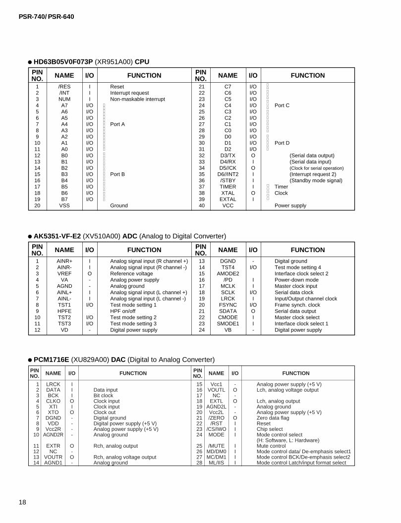
1 AINR+ I Analog signal input (R channel +) 13 DGND - Digital ground2 AINR- I Analog signal input (R channel -) 14 TST4 I/O Test mode setting 43 VREF O Reference voltage 15 AMODE2 Interface clock select 24 VA - Analog power supply 16 /PD I Power-down mode5 AGND - Analog ground 17 MCLK I Master clock input6 AINL+ I Analog signal input (L channel +) 18 SCLK I/O Serial data clock7 AINL- I Analog signal input (L channel -) 19 LRCK I Input/Output channel clock8 TST1 I/O Test mode setting 1 20 FSYNC I/O Frame synch. clock9 HPFE HPF on/off 21 SDATA O Serial data output10 TST2 I/O Test mode setting 2 22 CMODE I Master clock select11 TST3 I/O Test mode setting 3 23 SMODE1 I Interface clock select 112 VD - Digital power supply 24 VB - Digital power supply
1 /RES I Reset 21 C7 I/O2 /INT I Interrupt request 22 C6 I/O3 NUM I Non-maskable interrupt 23 C5 I/O4 A7 I/O 24 C4 I/O Port C5 A6 I/O 25 C3 I/O6 A5 I/O 26 C2 I/O7 A4 I/O Port A 27 C1 I/O8 A3 I/O 28 C0 I/O9 A2 I/O 29 D0 I/O
10 A1 I/O 30 D1 I/O Port D11 A0 I/O 31 D2 I/O12 B0 I/O 32 D3/TX O (Serial data output)13 B1 I/O 33 D4/RX I (Serial data input)14 B2 I/O 34 D5//CK O (Clock for serial operation)15 B3 I/O Port B 35 D6//INT2 I (Interrupt request 2)16 B4 I/O 36 /STBY I (Standby mode signal)17 B5 I/O 37 TIMER I Timer18 B6 I/O 38 XTAL O Clock19 B7 I/O 39 EXTAL I20 VSS Ground 40 VCC Power supply
PIN NAME I/O FUNCTIONNO.PIN NAME I/O FUNCTIONNO.
HD63B05V0F073P (XR951A00) CPU
PIN NAME I/O FUNCTIONNO.PIN NAME I/O FUNCTIONNO.
AK5351-VF-E2 (XV510A00) ADC (Analog to Digital Converter)
PCM1716E (XU829A00) DAC (Digital to Analog Converter)
PINNO.
123456789
10
11121314
I/O
IIIOIO----
O-O-
LRCKDATABCK
CLKOXTIXTO
DGNDVDD
Vcc2RAGND2R
EXTRNC
VOUTRAGND1
NAME
Data inputBit clockClock inputClock inputClock outDigital groundDigital power supply (+5 V)Analog power supply (+5 V)Analog ground
Rch, analog output
Rch, analog voltage output Analog ground
FUNCTION PINNO.
15161718192021222324
25262728
I/O
-O-O--OIII
IIII
Vcc1VOUTL
NCEXTL
AGND2LVcc2L/ZERO/RST
/CS/IWOMODE
/MUTEMD/DM0MC/DM1ML/IIS
NAME
Analog power supply (+5 V)Lch, analog voltage output
Lch, analog outputAnalog groundAnalog power supply (+5 V)Zero data flagResetChip selectMode control select (H: Software, L: Hardware)Mute controlMode control data/ De-emphasis select1Mode control BCK/De-emphasis select2Mode control Latch/input format select
FUNCTION

SN74HCU04NSR (XC723A00)SN74HCU04N (IG142250)Hex Inverter
1
2
3
4
5
6
7
1A
1Y
2A
2Y
3A
3Y
Vss
14
13
12
11
10
9
8
VDD
6A
6Y
5A
5Y
4A
4Y
SN74HC08NSR (XD831A00)HD74LVC08FP (XU720A00)Quad 2 Input AND
1
2
3
1A
1Y
42A
52B
62Y
7VSS
1B
14
13
12
VDD
4A
11 4Y
10 3B
9 3A
8 3Y
4B
TC74HC32AF (XN241A00)Quad 2 Input OR
1
2
3
1A
1Y
42A
52B
62Y
7GND
1B
14
13
12
Vcc
4A
11 4Y
10 3B
9 3A
8 3Y
4B
TC74HC138AF (XM970A00)TC74HC138AFEL (XW762A00)3 to 8 Demultiplexer
1
2
3
4
5
6
7
A
ASelect
Enable
Output
Output
B B
C C
G2A G2A
G2BG2B
G1 G1
Y7 Y7 Y5
Y4
Y3
Y2
Y1
Y0
Y6
16
15
14
13
12
11
10
Vcc
YO
Y1
Y2
Y3
Y4
Y5
8GND 9 Y6
SN74HC374ANSR (XQ042A00) Octal 3-State D-Type Flip-Flop
Q
D CKOE
Q
D CKOE
Q
D CKOE
Q
D CKOE
OUTPUTCONTROL
1Q
1D
2D
2Q
3Q
3D
4D
4Q
GND
1 20
2 19
3 18
4 17
5 16
6 15
7 14
8 13
9 12
10 11
Vcc
8Q
8D
7D
7Q
6Q
6D
5D
5Q
CLOCK
Q
DCKOE
Q
DCKOE
Q
DCKOE
Q
DCKOE
SN75C1168N (XU463A00)Line Driver / Receiver
1
2
3
4
5
6
7
1B
1A
1R
1DE
2R
2A
2B
16
15
14
13
12
11
10
Vcc
1D
1Y
1Z
2DE
2Z
2Y
8GND 9 2D
M5227P (XF751A00)5-Band Graphic Equalizer
1
2
3
4
5
6
7
IN1
NF1
IN2
NF2
IN3
NF3
IN4
16
15
14
13
12
11
10
-Vcc
GND
+Vcc
OUT
-IN
10k
10k
47k
47k
47k540
540
540
540
540
540
47k
47k
47k +IN
NF5
8NF4 9 IN5
+-
+-
+-
+-
+ -
+ -
LB1443N (XF483A00)LED Driver
1 2 3 4 5 6 7 8 9
GND IN VCCOUTD1 D2 D3 D4 D5
1
A
2 3 4 5 6 7 8 9
+V -IN -V
+INOUT
A A A
+V-IN
+IN OUT
BBB
-
+
B
-+
µPC4570HA (XB247A00)Dual Operational Amplifier
M5223AFP (XV117A00)M5223AL (XW373A00)Dual Operational Amplifier
1
2
3
4 -V
8
7
6
5
Output A +V
Non-InvertingInput A
Ground
+DC VoltageSupply
Output B
InvertingInput B
Non-InvertingInput B
InvertingInput A +-
+ -
DM: IC10,16(PSR-740) IC420(PSR-640)JACK: IC02
DM: IC15(PSR-740) IC370(PSR-640)
DM: IC14(PSR-740) IC360(PSR-640)
DM: IC13,19(PSR-740) IC350,510(PSR-640)DM: IC18,20(PSR-740) IC430,500(PSR-640) JACK: IC01
AM: IC210,220
DM: IC33(PSR-740)MIC: IC100(PSR-740)
MIC: IC001(PSR-740)
AM: IC320,510
IC BLOCK DIAGRAM
HD63266F (XI939A00) FDC (Floppy Disk Controller)
SED1335F0B (XQ595A00) LCDC (LCD Controller)
PSR-740/PSR-640
19
PINNO.
123456789
1011121314151617181920212223242526272829303132
I/O
IIIIIIIII
I/OI/OI/OI/OI/OI/OI/OI/OOOI
IIIIIII
8"//5"XTALSET/RESETE//RD
RW//WR/CS
/DACKRS0RS1
VSS1VSS2
D0D1D2D3D4D5D6D7
/DREQ/IRQ
/DENDVSS3
1/2 EX1VCC1NUM1NUM3
IFSSFORM
/INP/READY/WPRT
NAME
Data transmission speedClock selectRestEnable/ReadRead/write/WriteChip selectDMA acknowledge
Register select
Ground
Data bus
DMA requestInterrupt requestData endGround
Power supply
Host interface selectFormat dataIndex pulseReady from FDDWrite control signal
FUNCTION PINNO.
3334353637383940414243444546474849505152535455565758596061626364
I/O
III
OO
OOOO
OOOO
OOOO
/TRKO/INDEX/RDATAXTAL2
EXTAL2NC
XTAL1EXTAL1
VSS4VSS5
NCVCC2VCC3VCC4
/WGATE/WDATAVSS6/STEP/HDIR
/HLOAD/HSELVSS7/DS0/DS1/DS2/DS3VSS8
/MON0/MON1/MON2/MON3VSS9
NAME
Track 00 signalIndex signalRead data input from FDD
Clock
Clock
Ground
Power supply
Write controlWrit data to FDDGroundStep signal to control head of FDDDirectionHead loadHead selectGround
Drive select
Ground
Motor on
Ground
FUNCTION
PINNO.
123456789
101112131415161718192021222324252627282930
I/O
OOOOOOOO-I--IIIIIOII-
I/OI/OI/OI/OI/OI/OI/OI/OO
VA5VA4VA3VA2VA1VA0
/VWR/VCE/VRD/RESNCNC/RD/WRSEL2SEL1OSC1OSC2/CSA0VddD0D1D2D3D4D5D6D7
XD3
NAME
VRAM address bus
VRAM read/writeMemory controlNot usedInitial clearNot usedNot usedRead strobeWrite strobeBus selectBus selectClockClockChip selectData mode selectPower supply
Data bus
Data bus output for 4 bit dot
FUNCTION PINNO.
313233343536373839404142434445464748495051525354555657585960
I/O
OOOOO-OOOOOI/OI/OI/OI/OI/OI/OI/OI/OOOOOOOOOOO-
XD2XD1XD0
XECLXSCLVssLPWF
YDISYD
YSCLVD7VD6VD5VD4VD3VD2VD1VD0VA15VA14VA13VA12VA11VA10VA9VA8VA7VA6NC
NAME
Data bus output for 4 bit dot
S driver enable, chain clockData bus shift clock GroundX driver latch pulseFrame signal for X/Y driverPower down signal for displaying off modeScan start signalScan shift clock
VRAM data bus
VRAM address bus
Not used
FUNCTION

25
PSR-740/PSR-640
TEST NO. LCD (initial) Test Functions and Judgment Criteria
TEST PROGRAM
A. PREPARATION1) PA-6 (AC adaptor) is used.2) The volume is usually moved to the use position when no volume change is required.3) Measuring instruments: frequency counter, level meter (with JIS-C filter)
Note: Connect a stereo plug to the [PHONES] jack at 33 ohms.4) Jigs: foot switch, MIDI cable, floppy disk (2HD & 2DD)
B. HOW TO ENTER THE TEST PROGRAMAUTO MODE
While pressing the C3#, F3 and G3# keys, turn the [STANDBY/ON] switch on.MANUAL MODE
While pressing the C2#, F2 and G2# keys, turn the [STANDBY/ON] switch on.
C. PROCEEDING THROUGH THE TEST PROGRAMAUTO MODE
When the test program is started, the test is automatically executed.When confirmation is necessary, the test program stops operating and waits for the instruction. At this time, press the[START/STOP] button; the next test is automatically executed.
MANUAL MODEThe LCD will display “TEST” when entering the test program.To select the program number, use the [BACK] and [NEXT] buttons.To execute the test, press the [START/STOP] button.To proceed to the next test, press the [START/STOP] button.
D. TEST PROGRAM LIST
1 001: Version Displays ROM versionROM (Program, Wave) versions are displayed alternately on the LCD.
2 002: Rom Chk1 Checks the ROMThe test results appear on the LCD.
3 003: Ram Chk1 Checks all the RAMs that are connected to the CPUThe test results appear on the LCD.
4 004: WaveRomChk1 Checks the WAVE ROMs that are connected to the CPUThe test results appear on the LCD.
7 007: FDD Chk Insert the floppy disks one by one (2DD and 2HD).Checks the floppy disk drive unit
9 009: Eff1Ram Chk Checks the effect RAM110 010: Eff2Ram Chk Checks the effect RAM2
(PSR-740 only)
11 011: TG1 Chk Outputs the sine wave by changing the channels in sequence from C1 to C6
After auto-scaling is finished, individual keys can be played. (If playing two or more keys simultaneously, the first pressed key has priority to make a sound.)
13 013: Pitch Chk Connect the frequency counter to the [PHONES] jack.Sets PAN to Center and produces a signal at 440 +/- 0.22 Hz
Check that the correct signal is produced.14 014: Output R Connect the level meter (with a JIS-C filter) to the [PHONES] jack. (33 ohm load)
Set the [MASTER VOLUME] at maximum and check the output level (1 kHz).PHONES L: less than -50.0 dBm PHONES R: -8.0 dBm +/- 2 dB
Connect the monaural plugs of the level meter (with a JIS-C filter) to the [AUX OUT] jacks.AUX OUT L: less than -50.0 dBm AUX OUT R: -6.0 dBm +/- 2 dB

26
PSR-740/PSR-640
15 015: Output L Connect the level meter (with a JIS-C filter) to the [PHONES] jack. (33 ohm load)Set the [MASTER VOLUME] at maximum and check the output level (1 kHz).
PHONES L: -8.0 dBm +/- 2 dB PHONES R: less than -50.0 dBmConnect the monaural plugs of the level meter (with a JIS-C filter) to the [AUX OUT] jacks.
AUX OUT L: -6.0 dBm +/- 2 dB AUX OUT R: less than –50.0 dBm19 019: D/A Noise Connect the level meter (with a JIS-C filter) to the [PHONES] jack. (33 ohm load)
Set the [MASTER VOLUME] at maximum. Check D/A converter noise.PHONES L/R: Less than -72.0 dBm (PSR-740), Less than -80.0 dBm (PSR-640)
20 020: SW,LED Chk Check the switches on the panel.Press the switches that are displayed on the LCD. A pre-assigned note is output when
pressing the switch. (With some switches, the corresponding LED will light up.)The test results appear on the LCD.
21 021: All LED On Check that the all LEDs on the panel are on.22 022: Red LED On Check that the all red LEDs on the panel are on.
23 023: GreenLED on Check that the all green LEDs on the panel are on.28 028: All LCD On Check that all LCD dots are on. The LCD becomes black.
29 029: All LCD Off Check that all LCD dots are off. The LCD becomes white.31 031: Pedal1 Chk Connect the foot switch (FC-4 or FC-5) to the [FOOT SWITCH] jack.
Check that the C3 note is output when pressing and releasing the pedal and the C4 note isoutput when pressing the pedal again.
33 033: PB Chk Check that the C3 note is output when rotating the [PITCH BEND] wheel to minimum andthe C4 note is output when rotating it to maximum.
34 034: MOD Chk Check that the C3 note is output when rotating the [MODULATION] wheel to minimumand the C4 note is output when rotating it to maximum.
35 035: EXP Pedal Chk Connect the expression pedal (FC-7) to the [FOOT VOLUME] jack.Check that the C3 note is output and the LCD displays 0 when pressing the expression
pedal to the lowered position and the C4 note is output and the LCD displays 127 whenbacking it to the raised position.
37 037: Midi Chk After connecting the [MIDI IN] jack and [MIDI OUT] jack with a MIDI cable, execute thetest. Set the [HOST SELECT] switch to MIDI
Check that the C4 note is output and that the test results appear on the LCD.38 038: To Host Chk For factory test use only
39 039: MIC Chk Connect a microphone to the [MIC/LINE IN] jack and speak to it.(PSR-740 only) Set the [MIC/LINE] select switch to MIC and set the [INPUT VOLUME] at maximum.
Check that the voice is converted to the 1-octave- upper tone without noise.41 041: Rom Chk2 Checks the ROMs that are connected to the CPU.
The test results appear on the LCD.42 042: Ram Chk2 Checks the RAMs that are connected to the CPU.
The test results appear on the LCD.43 043: WaveRomChk2 Checks the WAVE ROM.
The test results appear on the LCD.46 046: BackUp Chk2 Performs the RAM back-up check.
Check that the display reads “NG,” then turn off the power switch.Enter the test program and perform the RAM back-up checks, then check again.
Check that the LCD displays “OK.” Note: Do not turn on the power switch by normal mode while standing by, as the
RAM data will be lost.47 047: Factory Set All the RAMs are initialized and set to the factory preset data when executing this test.
The results appear on the LCD.48 048: Test Exit Exit from the test program after executing this test.
* NOTE: The above tests Nos. 41-46 , require approximately 25 minutes to conduct.
If the time is not available to perform the tests, proceed the test No.47 by pressing several the [NEXT] button.

29
PSR-740/PSR-640
CAUTION
• All registration and UserStyle/Pad memory data,plus the other settingslisted above, will be erasedand/or changed when thedata initializationprocedure is carried out.
• Carrying out the datainitialization procedure willusually restore normaloperation if the PSR-740/640 freezes or begins toact erratically for anyreason.
All data can be initialized and restored to the factory preset condition by turning on the powerwhile holding the highest (rightmost) white key on the keyboard. “Now initializing the internalmemory...” will appear briefly on the display.
DATA INITIALIZATION
30
PSR-740/PSR-640
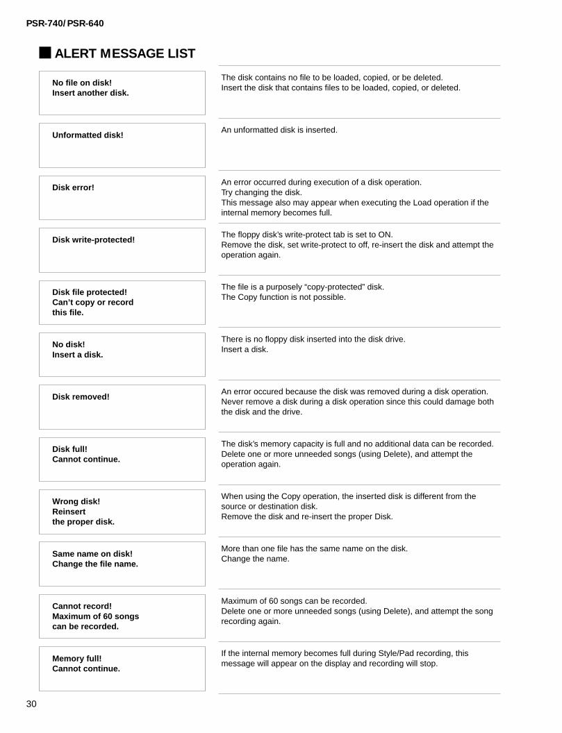
ALERT MESSAGE LIST
The file is a purposely “copy-protected” disk.The Copy function is not possible.
The disk contains no file to be loaded, copied, or be deleted.Insert the disk that contains files to be loaded, copied, or deleted.
An unformatted disk is inserted.
An error occurred during execution of a disk operation.Try changing the disk.This message also may appear when executing the Load operation if theinternal memory becomes full.
The floppy disk’s write-protect tab is set to ON.Remove the disk, set write-protect to off, re-insert the disk and attempt theoperation again.
There is no floppy disk inserted into the disk drive.Insert a disk.
An error occured because the disk was removed during a disk operation.Never remove a disk during a disk operation since this could damage boththe disk and the drive.
The disk’s memory capacity is full and no additional data can be recorded.Delete one or more unneeded songs (using Delete), and attempt theoperation again.
When using the Copy operation, the inserted disk is different from thesource or destination disk.Remove the disk and re-insert the proper Disk.
More than one file has the same name on the disk.Change the name.
Maximum of 60 songs can be recorded.Delete one or more unneeded songs (using Delete), and attempt the songrecording again.
If the internal memory becomes full during Style/Pad recording, thismessage will appear on the display and recording will stop.
No file on disk!Insert another disk.
Unformatted disk!
Disk error!
Disk write-protected!
Disk file protected!Can’t copy or recordthis file.
No disk!Insert a disk.
Disk removed!
Disk full!Cannot continue.
Wrong disk!Reinsertthe proper disk.
Same name on disk!Change the file name.
Cannot record!Maximum of 60 songscan be recorded.
Memory full!Cannot continue.

31
PSR-740/PSR-640
This message appears when you attempt to edit, quantize or clear thetrack which contains no data in the Record mode.
This message indicates that recording a new User style cannot be startedwhen all three User styles have recorded data. Make sure to clear at leastone of the three User styles before recording a new User style.
This message appears when you attempt to edit or quantize the track(other than RHYTHM) which contains preset data in the Style Recordmode.
This function cannot be used during Song/Style/Pad recording.
The MIDI function cannot be set during recording, playback, and diskoperations.
Harmony cannot be turned on during Style/Pad recording.
DSP cannot be turned on during Style/Pad recording.
This message appears to indicate you cannot enter the function when youselect Multi Pad function in the Multi Pad Recording mode.
The backup data is faulty.Use the data initialization function.
All data can be initialized and restore to the factory preset condition byturning the STANDBY switch ON while holding the highest (rightmost)white key on the keyboard.
This message may appear when the Host Select switch is set appropriatelyand the serial cable is connected to the TO HOST but not to the PC’s serialport (or the cable is properly connected to the PC which is currently turnedoff).
This message appears when executing the Quantize or Recordingoperations (in the Style Recording mode) when the internal memory is full.
Memory full!Clear unnecessary data.
Data not found!
User style full!
Cannot quantize thepreset data.
Cannot operateduring recording.
Cannot set the MIDIfunction during diskoperations, etc.
Cannot turn harmonyON during Style/Padrecording.
Cannot turn DSP ONduring Style/Padrecording.
Cannot enter thefunctions during Padrecording.
Backup error!
Now initializingthe internal memory...
Host is offline!

CPU
12
11
10
9
8
7
6
5
4
3
2
1
A B C D E F G H I J K L M N O P Q
12
11
10
9
8
7
6
5
4
3
2
1
A B C D E F G H I J K L M N O P Q
PSR-740 CIRCUIT DIAGRAM (DM1/2, MKS3, MKH, MKL, INV)
PSR-740 PSR-740
PSR-740
MKS3
MKH
DM
MKL
INV
L C D
to Back - light Assembly
Floppy Disk Drive
to PN1-CN8
to JACK-JK5
to AM-CN310
to MIC-JACK - CN5 to PN1-CN1
N.C.
to PN1-CN2CPU
FDC
SRAM 1M
DECODER
INVETER
EPROM MAIN1 32M
EPROM MAIN2 32M
OR
OR
OR
OR
AND
AND
D-FF
DECODER
D-FF
TRANSISTOR ARRAY
TRANSISTOR ARRAY
TRANSISTOR ARRAY
SRAM 256K
LCDC
INVERTER
INVERTER
DRAM 4M
DRAM 4M
FDC
REGULATOR +9V REGULATOR +5V
DC-DC CONVERTER
1/2
28CC1-8812655
28CC1-8811360
28CC1-8811360
2NA-8814265
28CC1-8814267
Note : See parts list for details of circuit board component parts
:
: Mylar Capacitor
: Metal Oxide Film Resistor
Ceramic Capacitor

12
11
10
9
8
7
6
5
4
3
2
1
A B C D E F G H I J K L M N O P Q
12
11
10
9
8
7
6
5
4
3
2
1
A B C D E F G H I J K L M N O P Q
PSR-740 CIRCUIT DIAGRAM (DM2/2, MIC-JACK, MIC)
PSR-740 PSR-740
PSR-740
DM
to DM-CN3to AM-CN320
MIC
MIC-JACK
SWP30B
VOP3
INVERTER
INVERTER
WAVE ROM LL 32M
WAVE ROM HL 32M
WAVE ROM LH 16M
WAVE ROM HH 16M
REGULATOR +3.3V
DRAM 4M
DRAM 4M
ADC
DAC
OP AMP
OP AMP
2/2LED DRIVER
0P AMP
0P AMP
MIC /LINE IN
28CC1-881426728CC1-8814268
28CC1-8814266
( )( )
not installedinstalled
(RE) (GR)
Note : See parts list for details of circuit board component parts
: Ceramic Capacitor: Semi-Conductive Ceramic Capacitor
560P
4.7K
5600p
100
18K
2.2K

CPU
12
11
10
9
8
7
6
5
4
3
2
1
A B C D E F G H I J K L M N O P Q
12
11
10
9
8
7
6
5
4
3
2
1
A B C D E F G H I J K L M N O P Q
PSR-640 CIRCUIT DIAGRAM (DM, MKS3, MKH, MKL, INV)
PSR-640 PSR-640
PSR-640
MKS3
MKH
DM
MKL
INV
to JACK-JK5
to PN1-CN8
to AM - CN320
to AM - CN310
L C D
Floppy Disk Drive
to PN1-CN2
to PN1-CN1
CPU
RESET
DECODER
SRAM 1M
PROGRAM1 ROM H 32M
PROGRAM2 ROM L32M
DRAM 16M
DECODER
DECODER
D-FF
DECODER
TRANSISTOR ARRAY
TRANSISTOR ARRAY
OR AND
AND
D - FF
SRAM 256K
LCDC
INVERTER
INVERTER
DC-DC CONVERTER
FDC
REGULATOR +5V
DAC
ROM WAVE1 32M
ROM WAVE2 32MSWX00B
REGULATOR +3.3V
DRAM 4M
to Back - light Assembly
28CC1-8812655
28CC1-8811360
28CC1-8811360
28CC1-8813199 2NA-8814265
Note : See parts list for details of circuit board component parts
: Ceramic Capacitor
: Mylar Capacitor
47
12
11
10
9
8
7
6
5
4
3
2
1
A B C D E F G H I J K L M N O P Q
12
11
10
9
8
7
6
5
4
3
2
1
A B C D E F G H I J K L M N O P Q
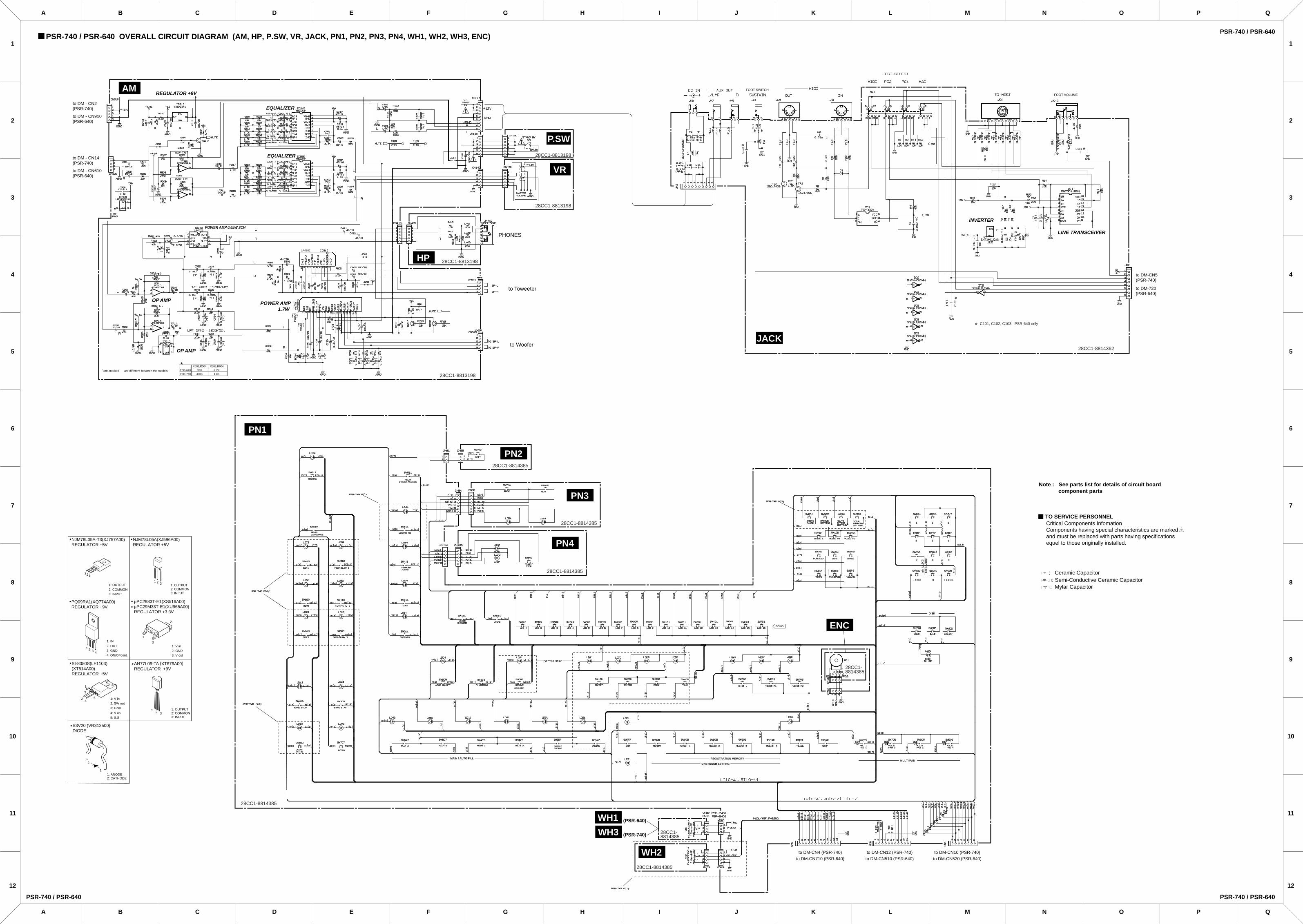
PSR-740 / PSR-640 OVERALL CIRCUIT DIAGRAM (AM, HP, P.SW, VR, JACK, PN1, PN2, PN3, PN4, WH1, WH2, WH3, ENC)
PSR-740 / PSR-640 PSR-740 / PSR-640
PSR-740 / PSR-640
JACK
PN1
PN2
PN3
PN4
ENC
WH2
WH1
WH3
AMto DM - CN2(PSR-740)
to DM - CN910(PSR-640)
to DM - CN14(PSR-740)
to DM - CN610(PSR-640)
to Toweeter
PHONES
to Woofer
to DM-CN5(PSR-740)
to DM-720(PSR-640)
+FOOT SWITCH
FOOT VOLUME
to DM-CN10 (PSR-740)
to DM-CN520 (PSR-640)
to DM-CN12 (PSR-740)
to DM-CN510 (PSR-640)
to DM-CN4 (PSR-740)
to DM-CN710 (PSR-640)
HP
P.SW
VR
Note : See parts list for details of circuit board component parts
TO SERVICE PERSONNELCritical Components InfomationComponents having special characteristics are markedand must be replaced with parts having specificationsequel to those originally installed.
: Ceramic Capacitor: Semi-Conductive Ceramic Capacitor
: Mylar Capacitor
REGULATOR +9V
POWER AMP 0.65W 2CH
POWER AMP 1.7W
OP AMP
OP AMP
EQUALIZER
EQUALIZER
INVERTER
LINE TRANSCEIVER
(PSR-640)
(PSR-740)
HELP/DIRECT ACCESS
/LANGUAGE
COUNTINTRO
INTRO
MAIN / AUTO FILL
SIMPLEENDING
ON / OFF
REGISTRATION MEMORYMULTI PAD
ONETOUCH SETTING
UTILITY
DISK
1 2 3
4 5 6
7 8 9
- / NO + / YES0
SONG
*
*
*
*
*PSR-640 39KPSR-740 470K
R503,R5042.2K1.8K
R603,R604
LA4525
28CC1-8813198
28CC1-8813198
28CC1-8813198
28CC1-8813198
28CC1-8814385
28CC1-8814385
28CC1-8814385
28CC1-8814385
28CC1-8814385
28CC1-8814385
28CC1-8814385
28CC1-8814362
Parts marked are different between the models.
NJM78L05A-T3(XJ757A00)REGULATOR +5V
123
1: OUTPUT2: COMMON3: INPUT
PQ09RA1(XQ774A00)REGULATOR +9V
2: OUT
1: IN
3: GND4: ON/OFcont.
4321
NJM78L05A(XJ596A00)REGULATOR +5V
1: OUTPUT2: COMMON3: INPUT
321
µPC2933T-E1(XS516A00)µPC29M33T-E1(XU965A00)REGULATOR +3.3V
1: V in2: GND3: V out
1
2
3
SI-8050S(LF1103)(XT514A00)REGULATOR +5V
1: V in2: SW out3: GND
4: V os5: S.S
1
3
24
5
DIODES3V20 (VR313500)
REGULATOR +9VAN77L09-TA (XT676A00)
213
3: INPUT2: COMMON1: OUTPUT
1: ANODE2: CATHODE
2
1
2200
p
2200
p
LA4262
C10
3 C101
C10
2
C101, C102, C103: PSR-640 only *
*
*
*
Recommended

![YQLW Qt UR]P U velikosti.pdfpsr 73/74/79/1 25 psr 140/160/1 75 psr 21 5/225 psr 260/270/280/290 psr 295/340/350 psr 540/550/730/740 psr 1000/2000 psr 1500/3000/8000 psr 9000 psr a300](https://img.dokumen.tips/doc/110x75/5e2699892211d34f32527d31/yqlw-qt-urp-u-psr-7374791-25-psr-1401601-75-psr-21-5225-psr-260270280290.jpg)


![Инструкция Yamaha PSR-E453PSR-E453/PSR-EW400 7 + " , . 4 " [ ] ( 5 .) ( 6&- " ), " . $ , . # "](https://img.dokumen.tips/doc/110x75/60dceb7003bf806879693103/f-yamaha-psr-e453-psr-e453psr-ew400-7-4-.jpg)