REDUCING CONTACT RESISTIVITY
IN GE-RICH SIGE MODULATORS
FOR OPTICAL INTERCONNECTS
A DISSERTATION
SUBMITTED TO THE DEPARTMENT OF ELECTRICAL
ENGINEERING
OF STANFORD UNIVERSITY
IN PARTIAL FULFILLMENT OF THE REQUIREMENTS
FOR THE DEGREE OF
BACHELORS IN ELECTRICAL ENGINEERING WITH HONORS
Zain Zaidi
May 2014

c© Copyright by Zain Zaidi 2014
All Rights Reserved

I certify that I have read this dissertation and that, in my opinion, it is
fully adequate in scope and quality as an undergraduate honors thesis.
James Harris
I certify that I have read this dissertation and that, in my opinion, it is
fully adequate in scope and quality as an undergraduate honors thesis.
Krishna Saraswat
This signature page was generated electronically upon submission of this dissertation
in electronic format. An original signed hard copy of the signature page is on file in
University Archives.
Acknowledgements
I would like to thank Professor James Harris for accepting me into his group and for
allowing me to explore my passion and interest. I have greatly benefitted from his
vast knowledge and experience in this field, and I am very grateful to him for taking
out the time to advice and mentor me.
I am also thankful to Professor Krishna Saraswat for agreeing to be a second
reader for this thesis. Despite being extremely busy with his own students, Professor
Krishna has always been very welcoming and helpful during his open door sessions
at his office.
I would like to express my immense gratitude to Ed Fei, my graduate mentor
during the time of my research. I thank him for always being available through
emails, text messages, and even odd hour phone calls. His readiness and patience to
teach me any theoretical concept or experimental technique was very inspiring.
I am also grateful to Xiaochi Chen for help with epitaxial growth and Kai Zang
for help with SEM imaging. I am also thankful to Dr. Yijie Huo and Professor Ted
Kamins for feedback and advice during the course of my research. I would also like
to thank Dr. Jason Lin for help with TiO2 processes and fabrication.
Most of the research presented in this thesis was performed in Stanford Nanofab-
rication Facility (SNF). I would like to thank Electrical Engineering’s REU program
and its coordinator, Meo Kittiwanich, for generously supporting my nanofabrication
costs. I am also grateful to SNF staff for assisting with my fabrication needs.
I am also very grateful to my loving parents for their prayers and unconditional
support during all phases of my life. I would like to thank them for being supportive
of my research endeavors, even if it meant not being able to see me for extended

periods of time.
Lastly, all this would not have been remotely possible without the generous do-
nation of Susan and Greg McCaw for supporting my undergraduate education at
Stanford. I am extremely thankful to them for not just being my donors, but also for
being my mentors. This thesis is dedicated to them.

Abstract
Interconnects have become a performance bottleneck as devices continue to scale
down. One way to solve this problem is to move to optical interconnects instead.
A key component for an interconnect system is the modulator. These modulators
have to be CMOS compatible so that they can be integrated with the current Silicon
based technologies. This can be achieved through fabricating Ge-rich Si0.20Ge0.80
P-I-N devices with Ge quantum wells separated by Si0.20Ge0.80 barriers.
A key challenge in making these modulators energy efficient and high speed is
reducing the contact resistivity between the metal contacts and the top N-doped
Ge-rich SiGe layer. While a lot of work has been done in the past to reduce the
contact resistivity in Silicon, Germanium, and even Silicon-rich Silicon Germanium
structures, Germanium-rich Silicon Germanium structures have received very little
attention.
This thesis discusses reducing contact resistivity in Ge-like SiGe modulators through
two methods: Dopant segregation and Metal-Insulator-Semiconductor (MIS) ap-
proach. We first discuss the challenges associated with implementing the dopant
segregation technique because of the requirement of a high temperature anneal step.
We then discuss the techniques that were used to fabricate the MIS based SiGe mod-
ulators that used TiO2 as the insulator layer. Using this technique, we managed to
almost completely depin the Fermi level and reduce the contact resistivity by 25x and
two orders of magnitude.
Contents
Acknowledgements
Abstract
1 Introduction 1
1.1 Motivation . . . . . . . . . . . . . . . . . . . . . . . . . . . . . . . . . 1
1.1.1 SiGe Modulators for Optical Interconnect . . . . . . . . . . . 1
1.2 Thesis Organization . . . . . . . . . . . . . . . . . . . . . . . . . . . . 5
2 Semiconductor Contacts 6
2.1 Fermi Level Pinning . . . . . . . . . . . . . . . . . . . . . . . . . . . 6
2.2 Methods to Reduce Contact Resistivity . . . . . . . . . . . . . . . . . 8
2.2.1 Dopant Segregation . . . . . . . . . . . . . . . . . . . . . . . . 8
2.2.2 Metal Insulator Semiconductor (MIS) Contacts . . . . . . . . 10
3 Contact Resistivty Measurement Structures 14
3.1 Linear Transfer Length Method . . . . . . . . . . . . . . . . . . . . . 14
3.2 Circular Transfer Length Method . . . . . . . . . . . . . . . . . . . . 17
4 Experiments and Results 21
4.1 Dopant Segregation Technique . . . . . . . . . . . . . . . . . . . . . . 21
4.1.1 Motivation . . . . . . . . . . . . . . . . . . . . . . . . . . . . . 21
4.1.2 Methodology and Results . . . . . . . . . . . . . . . . . . . . 22
4.1.3 Discussion . . . . . . . . . . . . . . . . . . . . . . . . . . . . . 22
4.2 Metal Insulator Semiconductor Technique . . . . . . . . . . . . . . . 24
4.2.1 Motivation . . . . . . . . . . . . . . . . . . . . . . . . . . . . . 24
4.2.2 Fabrication . . . . . . . . . . . . . . . . . . . . . . . . . . . . 27
4.2.3 Results and Discussion . . . . . . . . . . . . . . . . . . . . . . 30
5 Conclusions 34
5.1 Summary . . . . . . . . . . . . . . . . . . . . . . . . . . . . . . . . . 34
5.2 Future Work . . . . . . . . . . . . . . . . . . . . . . . . . . . . . . . . 35
Bibliography 36

List of Figures
1.1 Relative delay versus technology node as predicted by ITRS [1] . . . . 2
1.2 Building blocks of an optical interconnect system [2] . . . . . . . . . . 2
1.3 Vertical Photocurrent Absorption curve for a 3 QW structure. 3x
difference in absroption percentage was observed at around 1460 nm [3] 3
1.4 The cross-sectional view shows the structure of strain balanced Ge/SiGe
multiple quantum wells (MQWs) grown on silicon on a relaxed SiGe
buffer layer (not to scale). [4] . . . . . . . . . . . . . . . . . . . . . . 4
1.5 A cross-sectional view shows that the direct Aluminum/Titanium con-
tact to the N-doped Ge-rich SiGe. It also shows the general structure
of the SiGe Modulator without the stress/strain details of Fig. 1.4 . . 5
2.1 Schematic Energy Band diagram of a Schottky barrier with trapped
charges.[5] . . . . . . . . . . . . . . . . . . . . . . . . . . . . . . . . . 7
2.2 Diagram showing the deformation of the energy band induced by the
charged dopants on the semiconductor side of the Silicide/Germanide.
[6] . . . . . . . . . . . . . . . . . . . . . . . . . . . . . . . . . . . . . 8
2.3 Sheet Resistance of Ni/Ge vs RTA temperature. Reduction in contact
resistivity is due to NiGe formation.[7] . . . . . . . . . . . . . . . . . 9
2.4 Contact resistivity for NiSi, NiSi2, TiSi2 and CoSi2 contacts on Si.[8] 10
2.5 Contact resistivity for annealed Ti/Si0.8Ge0.2 interaface.[9] . . . . . . 10
2.6 Graph showing the variation of contact resistivity vs interfacial layer
growth time. A clear minimum can be seen beyond which the contact
resistance starts to increase[10] . . . . . . . . . . . . . . . . . . . . . 11

2.7 Band diagrams of metal-semiconductor interface a) without thin di-
electric b) with thin dielectric. Upon the insertion of a dielectric layer,
thermionic barrier decreases while the tunneling barrier increases.[10] 12
2.8 Conduction Band Offsets of common dielectrics to Germanium. TiO2
as the lowest offset.[11] . . . . . . . . . . . . . . . . . . . . . . . . . . 13
2.9 Relative Contact Resistivity of various MIS contacts. 1000x improve-
ment was achieved using TiO2.[11] . . . . . . . . . . . . . . . . . . . 13
3.1 A typical linear transfer length method test structure [12] . . . . . . . 15
3.2 Measurement configuration of a four point probe method [13] . . . . . 15
3.3 Tranfer Length Method Structures with a 4-point measurement con-
figuration . . . . . . . . . . . . . . . . . . . . . . . . . . . . . . . . . 16
3.4 A typical I-V curve of a metal-semiconductor schottky contact. . . . . 17
3.5 An example of the Resistance vs Separation curve for our TLM struc-
tures. Red circles show the actual data points while the blue line is
just a first order polynomial fit. . . . . . . . . . . . . . . . . . . . . . 18
3.6 Design of a circular TLM strucuture. R is the outer radius whereas r
is the inner radius. Black area represents the metal and the white area
is the semiconductor. . . . . . . . . . . . . . . . . . . . . . . . . . . . 19
3.7 4-Point Probe setup on the circular TLM structure . . . . . . . . . . 19
3.8 Layout of multiple circular TLM structures on the wafer. The conse-
quent structures had different inner radiai [12] . . . . . . . . . . . . . 20
4.1 A schematic diagram of our structure. We hoped that annealing the
structure would lead to the formation of TiGe2. . . . . . . . . . . . . 22
4.2 Contact Resistivty as a function of anneal temperature for the struc-
tures shown in Fig. 4.4. . . . . . . . . . . . . . . . . . . . . . . . . . 23
4.3 Cross-sectional schematic of the modulator structures that were an-
nealed . . . . . . . . . . . . . . . . . . . . . . . . . . . . . . . . . . . 24
4.4 SEM image of the cross section of the modulator device after anneal-
ing at a high temperature. Red arrow indicates the penetration of
the metal/Germanide into the whole structure that is responsible for
shorting the P and N layers. 620nm is total distance between the N
doped and P doped layer. . . . . . . . . . . . . . . . . . . . . . . . . 25
4.5 Total TiSi2 thickness as a function of temperature and anneal time. [14] 26
4.6 Tcrit for TiGe2 and TiSi2 extrapolated by using Eq. 4.1 . . . . . . . . 26
4.7 The final schematic of the SiGe modulator with TiO2 to depin the
Fermi level. x indicates that the modulator was fabricated with differ-
ent thicknesses of TiO2. . . . . . . . . . . . . . . . . . . . . . . . . . 27
4.8 The P-I-N structure grown epitaxially. Multiple Ge quantum wells
separated by SiGe barriers were in the intrinsic region . . . . . . . . . 28
4.9 SiGe was dry etched to expose the P-doped layers. 200nm of PECVD
Oxide was grown on the wafer for electrical isolation of the P and
N-doped exposed layers. . . . . . . . . . . . . . . . . . . . . . . . . . 28
4.10 Contact plugs were etched for the N-layer. TiO2, Ti and Al were
deposited. . . . . . . . . . . . . . . . . . . . . . . . . . . . . . . . . . 29
4.11 TiO2 deposition thickness as a function of the number of cycles on
Savannah S200 Thermal ALD system . . . . . . . . . . . . . . . . . . 29
4.12 The structure after etching TiO2 by using Al as a hard mask. . . . . 30
4.13 IV curve of a Metal/N doped SiGe junction before and after the inser-
tion of TiO2 between the metal and semiconductor layers. . . . . . . 31
4.14 Contact Resistivity as a function of TiO2 thickness for devices with an
N layer doping of 7e18 cm−3 . . . . . . . . . . . . . . . . . . . . . . . 32

Chapter 1
Introduction
1.1 Motivation
Transistor dimensions have been scaling by a factor of 0.7x every two years, reaf-
firming the trend commonly known as Moore’s Law[15].Fig 1.1 shows the trends of
relative delay for the gate, local interconnects, and global interconnects as predicted
by the International Technology Roadmap for Semiconductors (ITRS). For smaller
technology nodes, the delay of the electrical interconnects, instead of that of the
transistor, is what limits the performance of the integrated circuit. This problem is
commonly referred to as the interconnect bottleneck.
1.1.1 SiGe Modulators for Optical Interconnect
One possible solution to this problem is to switch over to optical interconnects. The
components of an optical interconnect system are shown in Fig.1.2. Of these, the light
source, waveguide, modulator and photo-detector, are the four components exclusive
to the optical interconnect system. The challenge then is to implement a CMOS
compatible optical interconnect network.
Due to the absence of an efficient light emitter in group IV elements [16], mod-
ulators are favored over direct-driven lasers. Si waveguides employing total internal
reflection can be efficiently used to guide light. The main complexity thus lies in
1

Figure 1.1: Relative delay versus technology node as predicted by ITRS [1]
Figure 1.2: Building blocks of an optical interconnect system [2]
the modulator and the light detector. There are two main ways to modulate light
fast enough to be used in optical interconnects: Refractive modulators and Electro-
Absorption modulators. Refractive Modulators operate by interfering a beam with
2

CHAPTER 1. INTRODUCTION 3
itself. Although challenges in realizing these can be resolved by using micro-ring res-
onators to slow light, these kinds of modulators remain very temperature dependent.
The second main category of modulators, Electro-absorption modulator, functions
by changing the optical absorption of a semiconductor by applying voltage, and thus
Electric Field, to it. Electro-absorption modulators that function through the quan-
tum confined Stark effect in thin quantum well layers demonstrate spectrally abrupt
and stronger changes in the absorption coefficient [17].
It has been demonstrated that the quantum confined Stark effect (QCSE) in Ge
quantum wells is an efficient and strong electro-absorption mechanism for CMOS and
Silicon compatible modulators [4] [18] [19]. These QCSE SiGe modulators have been
shown to demonstrate high absorption contrast for a very small applied voltage bias
as evident in Fig. 1.3 [3].
Figure 1.3: Vertical Photocurrent Absorption curve for a 3 QW structure. 3x differ-ence in absroption percentage was observed at around 1460 nm [3]
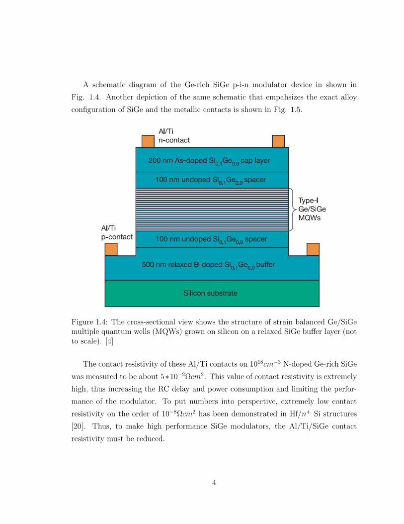
A schematic diagram of the Ge-rich SiGe p-i-n modulator device in shown in
Fig. 1.4. Another depiction of the same schematic that empahsizes the exact alloy
configuration of SiGe and the metallic contacts is shown in Fig. 1.5.
Figure 1.4: The cross-sectional view shows the structure of strain balanced Ge/SiGemultiple quantum wells (MQWs) grown on silicon on a relaxed SiGe buffer layer (notto scale). [4]
The contact resistivity of these Al/Ti contacts on 1018cm−3 N-doped Ge-rich SiGe
was measured to be about 5∗10−2Ωcm2. This value of contact resistivity is extremely
high, thus increasing the RC delay and power consumption and limiting the perfor-
mance of the modulator. To put numbers into perspective, extremely low contact
resistivity on the order of 10−8Ωcm2 has been demonstrated in Hf/n+ Si structures
[20]. Thus, to make high performance SiGe modulators, the Al/Ti/SiGe contact
resistivity must be reduced.
4

CHAPTER 1. INTRODUCTION 5
Figure 1.5: A cross-sectional view shows that the direct Aluminum/Titanium con-tact to the N-doped Ge-rich SiGe. It also shows the general structure of the SiGeModulator without the stress/strain details of Fig. 1.4
1.2 Thesis Organization
In this thesis, we first study the common methods used to reduce contact resistivity
in Si, Ge and Si-rich SiGe structures in Chapter 2. In this chapter, we also discuss the
underlying physics behind this particular technique and provide examples of Fermi
level depinning through their implementation.
In Chapter 3, we then discuss the design of different devices that were used to
measure contact resistivity, ρc. We also supplement these designs with equations to
highlight the calculations necessary to accurately calculate ρc.
The details of our experiments and our results are then shown in Chapter 4.
We also discuss the results and their implication for the modulator structure in this
chapter.
Finally, in chapter 5, we provide a brief summary of all the work that we have
shown in this thesis. We then briefly discuss the relevant future steps for this project.
Chapter 2
Semiconductor Contacts
This chapter discusses the mechanisms that are responsible for the high contact re-
sistance in semiconductors and some of the approaches that have been used to reduce
it.
2.1 Fermi Level Pinning
The I-V curve of a metallic contact is ideally expected to be Ohmic. However, the
formation of a Schottky barrier when a metal is placed directly on a semiconductor
disrupts this ideal behavior. The n-type barrier height can be approximated by Eq.
2.1.
ΦB0 = φM − χS (2.1)
Where φM is the Metal workfunction and χS is the semiconductor electron affinity.
ΦB0, the barrier height, then is the energy required to excite an electron from the
Fermi Level, EF , to the conduction minimum [21].
When a metal is in contact with a semiconductor, a chemical reaction occurs at the
interface between the metal and the semiconductor and causes interface defects [22].
A few layers from the semiconductor metal interface, there is a significant amplitude of
the continuum of states around the Fermi Level because of these chemical reactions.
6

CHAPTER 2. SEMICONDUCTOR CONTACTS 7
The induced intrinsic Bloch states with complex wave vector in the energy gap of
bulk semiconductor are referred to as the Metal Induced Gap States (MIGS). A small
density of these MIGS is thus sufficient to pin the Fermi Level [23].
Fig. 2.1 shows the band diagram of a classic Schottky barrier. φM is the Metal
workfunction and ΦnSB is the barrier height, same as ΦB0 in Eq. 2.1. MIGS cause a
much lower dependence of the band bending, qVB, on metal work function, φM .
The degree of Fermi Level pinning is commonly denoted by the parameter 1 >=
S >= 0, Where S = 1 denotes no pinning and S = 0 denotes perfect pinning.
Emperically, S obeys Eq. 2.2 [24].
S =1
1 + 0.1(ε∞ − 1)2(2.2)
Where ε∞ is the electronic part of the dielectric constant. The S factor in Germa-
nium is reported to be extremely low, betwen 0.02 [25] and 0.05 [26], indicating very
strong pinning. The S factor for Si has been estimated to be between 0.09 to 0.27,
also indicating strong Fermi Level pinning, but not as strong as that in Ge[27, 28].
Figure 2.1: Schematic Energy Band diagram of a Schottky barrier with trappedcharges.[5]
2.2 Methods to Reduce Contact Resistivity
Contact resistivity can be reduced by two primary techniques: increasing the semi-
conductor doping concentration, and depinning the Fermi level. Silicon Germanium
used in the modulator structure was epitaxially grown and doped. Thus common
techniques to increase doping concentration such as laser annealing [29, 30] were not
applicable. Several techniques have been explored to depin the Fermi Level and they
are briefly discussed in this section.
2.2.1 Dopant Segregation
Silicides and germanides form at the metal-Silicon / Metal-Germanium interfaces
can segregate dopants at the semiconductor interface, and this can partially depin
the Fermi level. There are multiple theories that attribute dopant segregation to
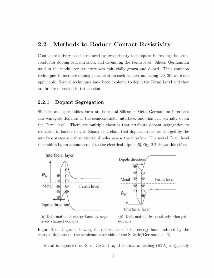
reduction in barrier height. Zhang et al claim that dopant atoms are charged by the
interface states and form electric dipoles across the interface. The metal Fermi level
then shifts by an amount equal to the electrical dipole [6].Fig. 2.2 shows this effect.
(a) Deformation of energy band by nega-tively charged dopants
(b) Deformation by positively chargeddopants
Figure 2.2: Diagram showing the deformation of the energy band induced by thecharged dopants on the semiconductor side of the Silicide/Germanide. [6]
Metal is deposited on Si or Ge and rapid thermal annealing (RTA) is typically
8
CHAPTER 2. SEMICONDUCTOR CONTACTS 9
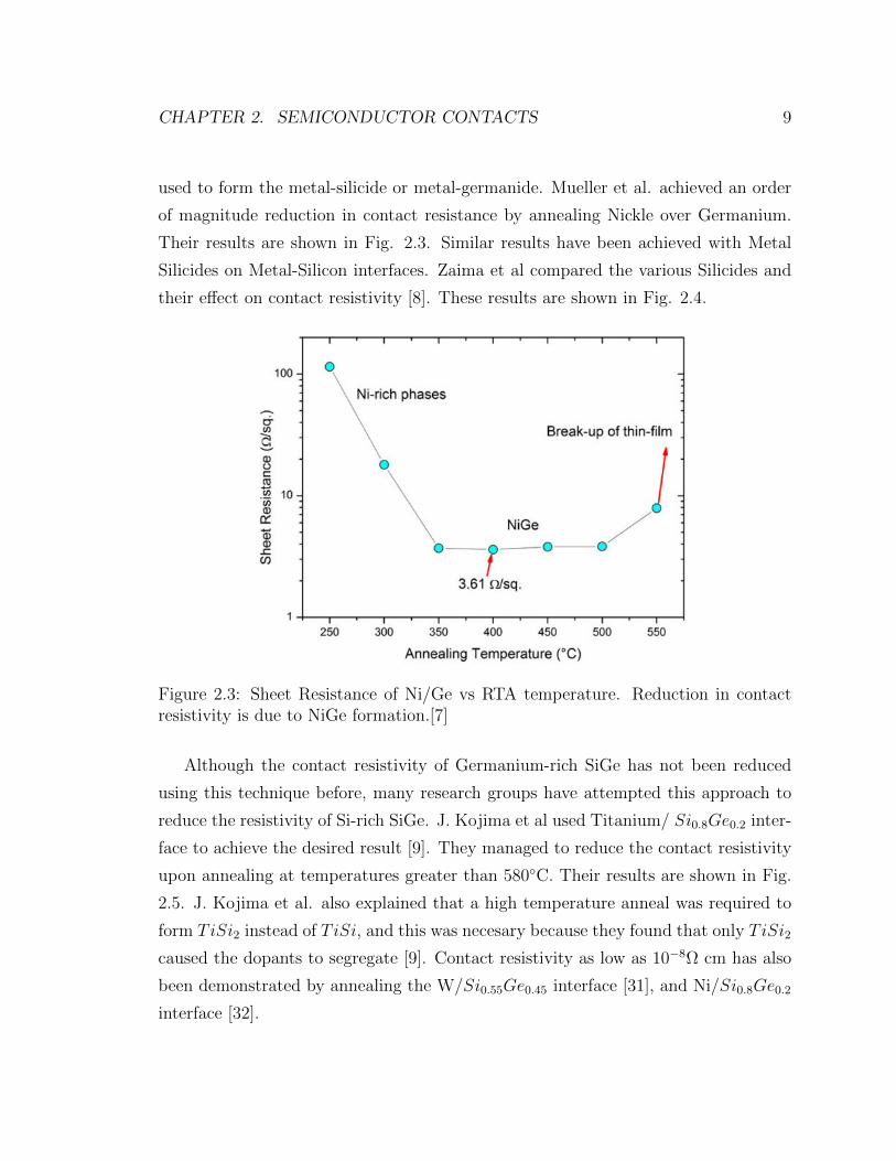
used to form the metal-silicide or metal-germanide. Mueller et al. achieved an order
of magnitude reduction in contact resistance by annealing Nickle over Germanium.
Their results are shown in Fig. 2.3. Similar results have been achieved with Metal
Silicides on Metal-Silicon interfaces. Zaima et al compared the various Silicides and
their effect on contact resistivity [8]. These results are shown in Fig. 2.4.
Figure 2.3: Sheet Resistance of Ni/Ge vs RTA temperature. Reduction in contactresistivity is due to NiGe formation.[7]
Although the contact resistivity of Germanium-rich SiGe has not been reduced
using this technique before, many research groups have attempted this approach to
reduce the resistivity of Si-rich SiGe. J. Kojima et al used Titanium/ Si0.8Ge0.2 inter-
face to achieve the desired result [9]. They managed to reduce the contact resistivity
upon annealing at temperatures greater than 580C. Their results are shown in Fig.
2.5. J. Kojima et al. also explained that a high temperature anneal was required to
form TiSi2 instead of TiSi, and this was necesary because they found that only TiSi2
caused the dopants to segregate [9]. Contact resistivity as low as 10−8Ω cm has also
been demonstrated by annealing the W/Si0.55Ge0.45 interface [31], and Ni/Si0.8Ge0.2
interface [32].

Figure 2.4: Contact resistivity for NiSi, NiSi2, TiSi2 and CoSi2 contacts on Si.[8]
Figure 2.5: Contact resistivity for annealed Ti/Si0.8Ge0.2 interaface.[9]
2.2.2 Metal Insulator Semiconductor (MIS) Contacts
This technique involves the insertion of an ultra-thin dielectric layer between the
metal and the semiconductor to produce a tunnel junction that can reduce the con-
tact resistivity. This extremely thin layer of a larger band gap material reduces the10

CHAPTER 2. SEMICONDUCTOR CONTACTS 11
penetration of metal electron wave function and leads to a reduction in MIGS. The
first known experimental application of this technique was the insertion of Si3N4 to
reduce the contact resistivity in Silicon contacts by Conally et al. [10]. The authors
of this paper also observed that although there was a clear minimum of contact resis-
tivity, increasing the thickness of the dielectric thickness beyond this minimum point
causes the blocking of electron tunneling and thus increasing the contact resistance.
This trend is shown in Fig. 2.6.
Figure 2.6: Graph showing the variation of contact resistivity vs interfacial layergrowth time. A clear minimum can be seen beyond which the contact resistancestarts to increase[10]
Thus as explained by Conally et al, there are two primary principles responsible for
the reduction in contact resistivity and its eventual rise in MIS contacts. The dielectric
reduces the penetration of electron wavefunction and this leads to the reduction in
MIGS and a decreased thermionic barrier. While the presence of the dielectric layer
between the metal and the semiconductor also introduces a tunneling barrier. Hence
there is a clear tradeoff. As the thickness of the dielectric increases, the thermionic
barrier decreases and this tends to decrease the contact resistance. However, it also
increases the tunneling barrier and this tends to increase the contact resistance. The

band diagrams before and after the insertion of dielectrics are shown in Fig. 2.7.
Figure 2.7: Band diagrams of metal-semiconductor interface a) without thin dielectricb) with thin dielectric. Upon the insertion of a dielectric layer, thermionic barrierdecreases while the tunneling barrier increases.[10]
Si3N4 has also been used to depin the Fermi level in Ge contacts [33]. Similarly,
Aluminum Oxide has been used to depin Fermi level is both Silicon and Germanium
[34] [35]. However, in all these dielectrics, the tunneling barrier effect starts to domi-
nate after just a few nanometers of the inserted dielectric layer. Thus the Fermi level
is only partially de-pinned and very low contact resistivity values cannot be achieved.
The thickness of the dielectric where the tunneling barrier starts to dominate can
be increased by using a dielectric with a low conduction band offset to that of the
semiconductor. Ge-rich SiGe’s properties are closer to that of Germanium. Jason Lin
compared the Conduction Band Offsets (CBO) of common dielectrics to Germanium
[11] and his comparison is shown in Fig. 2.8. Due to the extremely low CBO of TiO2,
Jason Lin et al. used TiO2 as a dielectric to depin the Fermi Level in N+ Germanium
[36]. They managed to achieve a 1000x reduction in contact resistivity using TiO2
between Metal and Germanium interface [37]. Their results are shown in Fig. 2.9.
12

CHAPTER 2. SEMICONDUCTOR CONTACTS 13
Figure 2.8: Conduction Band Offsets of common dielectrics to Germanium. TiO2 asthe lowest offset.[11]
Figure 2.9: Relative Contact Resistivity of various MIS contacts. 1000x improvementwas achieved using TiO2.[11]

Chapter 3
Contact Resistivty Measurement
Structures
This chapter discusses the techniques used to measure the Ge-rich SiGe contact resis-
tivity. Linear and circular Tranfer Length Method (TLM) structures were both used
to measure the contact resistivity and the values were compared.
3.1 Linear Transfer Length Method
The linear TLM structure comprised 11 contacts which were arranged in a manner
similar to that shown in Fig. 3.1. The spacing between each consecutive contact
for our TLM structures was different and varied evenly from 10 µm to 100 µm. An
isolation etch was first done to isolate these contact structures from the rest of the
devices on the wafer. Four consecutive pads were then chosen and current was driven
through the outer two contacts while the voltage difference was measured between
the inner two contacts. This measurement technique is similar to the 4-Point probe
method shown in Fig. 3.2 and enabled us to compensate for the resistance of the
probes. Our measurement setup which combined the traditional TLM structures and
the 4-point probe measurement technique is shown in Fig. 3.3.
In the structures with no insulator layer, the I-V characteristic curve of the con-
tacts was a Schottky diode curve instead of a linear Ohmic curve because of the
14

CHAPTER 3. CONTACT RESISTIVTY MEASUREMENT STRUCTURES 15
Figure 3.1: A typical linear transfer length method test structure [12]
Figure 3.2: Measurement configuration of a four point probe method [13]
pinning of the Fermi Level. An example of such a characteristic IV curve is shown in
Fig. 3.4. For such contacts where the Fermi Level was pinned, we used the effective
resistance at the two values of bias, -1v and -2v. Due to the nonlinear nature of these
curves, the resistance varied at every voltage bias and the voltage values of -1v and
-2V were chosen because the SiGe modulator was operated around these values of
voltage. For the contacts in which the Fermi level was depinned, the I-V curve was
almost linear and we used the gradient of a first order polynomial fit as the resistance
of that contact.
Once the resistance was found by probing the consecutive contacts, resistance was

Figure 3.3: Tranfer Length Method Structures with a 4-point measurement configu-ration
plotted as a function of the distance between the particular consecutive contacts.
Graphing software was then used to draw the first order polynomial fit between the
data points. An example of a curve depicting resistance as a function of separation
(between consecutive contacts) is shown in Fig. 3.5. The gradient and y-intercept of
such best fit line can then be calculated.
Using the gradient and the y-intercept of the best fit line, we can find the sheet
resistance and the transfer length through the following equations:
Rsh = m ∗ Z (3.1)
LT =c
2m(3.2)
Where m is the gradient and c is the y intercept of the best fit line. Z is the width
of the individual TLM contact pads and in our design, Z = 200 um. Rsh is the sheet
resistance and LT is the transfer length. Using the values of Rsh and LT from Eq.
16

CHAPTER 3. CONTACT RESISTIVTY MEASUREMENT STRUCTURES 17
Figure 3.4: A typical I-V curve of a metal-semiconductor schottky contact.
3.1 and Eq. 3.2 respectively, we used Eq. 3.4 to find the Contact Resistivity, ρc.
ρc = L2T ∗Rsh (3.3)
We can also use Eq. 3.1 and the thickness of the doped layer, t, to find the sheet
resistivity, ρsh, through the following equation:
ρsh = Rsh ∗ t (3.4)
3.2 Circular Transfer Length Method
In addition to the linear TLM structures, we also used circular TLM structures. The
design of this structure is shown in Fig. 3.6. The 4-point measurement configuration
on the circular TLM structure is shown in Fig. 3.7. Similar to the linear TLM, about
10 circular TLM structures were fabricated with the inner radius, r, varying from
10µm to 100µm. The overall design was similar to that in Fig. 3.8.
The method to calculate the contact resistivity in circular TLM structures is very

Figure 3.5: An example of the Resistance vs Separation curve for our TLM struc-tures. Red circles show the actual data points while the blue line is just a first orderpolynomial fit.
similar to that used to calculate in linear structures. Eq. 3.2 and Eq 3.4 still hold
true. However, the width, w, in Eq. 3.1 is replaced with the circumference of the disk.
Eq 3.5 is thus used to calculate the Sheet Resistance in circular TLM structures.
Rsh = m ∗ 2πr (3.5)
Where r is the inner radius of the structure as shown in Fig. 3.6.
18

CHAPTER 3. CONTACT RESISTIVTY MEASUREMENT STRUCTURES 19
Figure 3.6: Design of a circular TLM strucuture. R is the outer radius whereas r is theinner radius. Black area represents the metal and the white area is the semiconductor.
Figure 3.7: 4-Point Probe setup on the circular TLM structure

Figure 3.8: Layout of multiple circular TLM structures on the wafer. The consequentstructures had different inner radiai [12]
20

Chapter 4
Experiments and Results
This chapter describes the methods and results of the experiments we performed to
reduce the contact resistivity in Ge-rich SiGe structures. The alloy concentration
in our SiGe was about Si0.2Ge0.8. The two techniques we used to depin the Fermi
level were the dopant segregation technique and the Metal Insulator Semiconductor
approach.
4.1 Dopant Segregation Technique
4.1.1 Motivation
The physics behind the dopant segregation technique and its use to depin the Fermi
level in Si, Ge and Si-rich SiGe structures has already been discussed in chapter 2.2.1.
The use of Titanium Silicide to depin the Fermi level level in Si0.8Ge0.2 structures
by J. Kojima et al. holds particular relevance to our structures. Their method and
results were discussed in Chapter 2.
In our structures, we used Aluminum to make contacts for our Si0.20Ge0.80 modu-
lator. Since the adhesion between Aluminum and Silicon and Germanium is poor, we
used Titanium as an adhesion layer between Aluminum and SiGe. Thus, similar to
the design of J. Kojima et al. with an Al/Ti/Si stack, we had an Al/Ti/SiGe stack
and this technique appealed to us because it only required annealing.
21

4.1.2 Methodology and Results
We postulated that similar to J. Kojima et al, annealing an Al/Ti/SiGe stack would
lead to the formation of Al/TiGe2/SiGe interface. The schematic for this design is
drawn in Fig. 4.4. We annealed our samples in an N2 ambient for 30s at different
temperatures using the Allwin 610 Rapid Thermal Process Systems. The ramp up
time was about 10 seconds while the ramp down typically lasted for about a minute.
The effect of different anneal times on the contact resistivity is shown in Fig. 4.2.
(a) Before Anneal
(b) After anneal
Figure 4.1: A schematic diagram of our structure. We hoped that annealing thestructure would lead to the formation of TiGe2.
4.1.3 Discussion
As evident in Fig. 4.2, contact resistivity increased for structures that were annealed
at lower temperatures. This is not unexpected and may be attributed to the formation
of TiGe instead of TiGe2 similar to what J. Kojima et al. concluded for TiSi. We
did, however, expect the contact resistivity to be much lower for the samples that
were annealed at higher temperatures.
The full cross-sectional schematic of the modulator structures that were annealed
is shown in Fig. 4.3. As Fig. 4.2 shows, annealing the samples at high temperatures
resulted in shorts between the P and N doped layers of the device. Therefore, instead
of measuring the N layer contact resistivity, we measured the P doped layer’s contact
resistivity when the N-layer contact was probed. This behavior was unexpected and
thus we decided to investigate it.
22

CHAPTER 4. EXPERIMENTS AND RESULTS 23
Figure 4.2: Contact Resistivty as a function of anneal temperature for the structuresshown in Fig. 4.4.
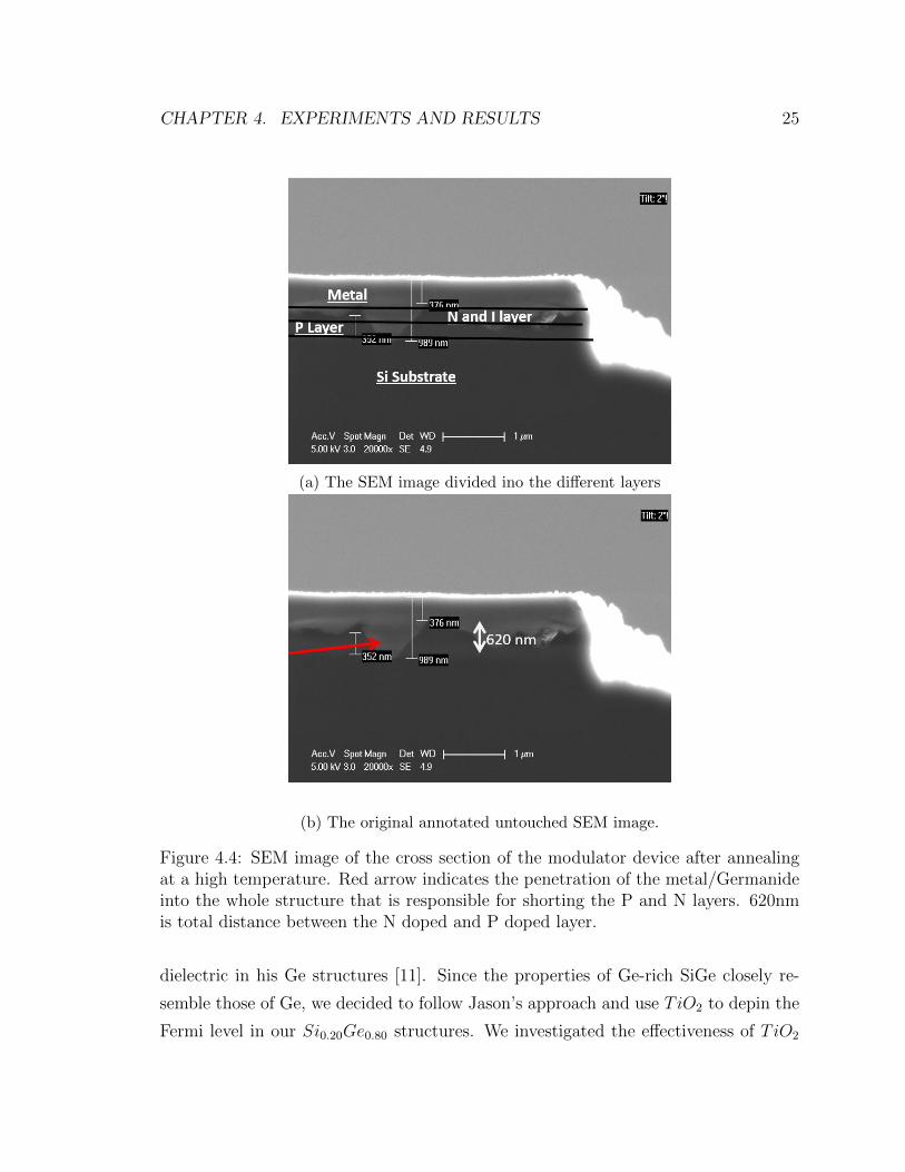
The Scanning Electron Microscopy (SEM) image of the cross section of a device
that was annealed at a high temperature is shown in Fig. 4.4. As evident in the
figure, the Metal/Germanide layer is penerating through the entire structure, and
thus shorting the P and N doped layers. One potential explanation of this might
be that despite the presence of a thin Titanium layer, Aluminum diffused into SiGe
because of annealing at higher temperatures. While plausible, the presence of the
Titanium layer and the slow diffusion of Al in SiGe makes it extremely hard for the
metal to penetrate about 620nm through the whole structure.
Another plausible explanation for the observed effect is that TiGe2 penetrated
through the structure. D. Levy et al. characterized the formation of TiSi2 by an-
nealing Titanium on Silicon. Their results are shown in Fig. 4.5. We define the
‘critical anneal temperature’, Tcrit, as the temperture at which 620nm of TiSi2 or
TiGe2 formed, sufficient to short our P and N layers. It can be seen through their

Figure 4.3: Cross-sectional schematic of the modulator structures that were annealed
results that to form about 620nm of TiSi2, Titanium and Silicon have to be annealed
at 750C for 30s. Thus for a 30 second anneal, Fig. 4.5 tells us that the Silicide’s
Tcrit is about 750C.
Germanium and Silicon have different melting points. Silicon melts at 1414C, a
temperature that is much higher than Germanium’s melting point at approximately
938.2C. Using the difference in the melting points, we can extrapolate the thickness
data taken by D. Levy et al. to obtain rough values for the Germides Tcrit for a 30
second anneal using the following equation:
Tcrit,Germanide = Tcrit,Silicide ∗Tmp,Ge
Tmp,Si
(4.1)
Where Tcrit is the critical anneal temperature and Tmp is the melting point tem-
perature. This extrapolation for TiGe2 is graphically represented in Fig. 4.6. As
indicated by this figure, Tcrit for TiGe2 is calculated to be about 500C, the approx-
imate temperature at which we start seeing shorts in Fig. 4.2.
4.2 Metal Insulator Semiconductor Technique
4.2.1 Motivation
MIS technique and its underlying physics was extensively discussed in Chapter 2.2.2.
Lin, et al., achieved a 1000x reduction in contact resistivity by using TiO2 as the
24
CHAPTER 4. EXPERIMENTS AND RESULTS 25
(a) The SEM image divided ino the different layers
(b) The original annotated untouched SEM image.
Figure 4.4: SEM image of the cross section of the modulator device after annealingat a high temperature. Red arrow indicates the penetration of the metal/Germanideinto the whole structure that is responsible for shorting the P and N layers. 620nmis total distance between the N doped and P doped layer.
dielectric in his Ge structures [11]. Since the properties of Ge-rich SiGe closely re-
semble those of Ge, we decided to follow Jason’s approach and use TiO2 to depin the
Fermi level in our Si0.20Ge0.80 structures. We investigated the effectiveness of TiO2

Figure 4.5: Total TiSi2 thickness as a function of temperature and anneal time. [14]
Figure 4.6: Tcrit for TiGe2 and TiSi2 extrapolated by using Eq. 4.1
in depinning the Fermi level, and the optimal thickness of TiO2 to achieve the lowest
contact resistivity. Since the N-doping in our structures was much lower and on the
26

CHAPTER 4. EXPERIMENTS AND RESULTS 27
order of 5e18 cm−3, we also compared it with the different doping concentrations that
Jason Lin et al. had used in their structures.
4.2.2 Fabrication
The cross-sectional schematic of the final fabricated Si0.20Ge0.80 modulator with a
TiO2 layer is shown in Fig. 4.7. Many modulators were fabricated with different
thicknesses of the TiO2 layer. Furthermore, a TiO2 layer was not inserted for the P-
doped layer contacts because they were not pinned, and adding the TiO2 there would
have simply deteriorated the P junction contact resistivity. This section describes
how the final structure in Fig. 4.7 was fabricated.
Figure 4.7: The final schematic of the SiGe modulator with TiO2 to depin the Fermilevel. x indicates that the modulator was fabricated with different thicknesses ofTiO2.
The basic P-I-N layers with the Ge quantum wells in the intrinsic layer were first
epitaxially grown. Typical values for the N and P doping were about 5e18 cm−3 and
7e18cm−3, respectively. The structure after the epitaxial growth is shown in Fig.
4.8. Dry etching was then performed in an O2 and CHF3 ambient to etch away the
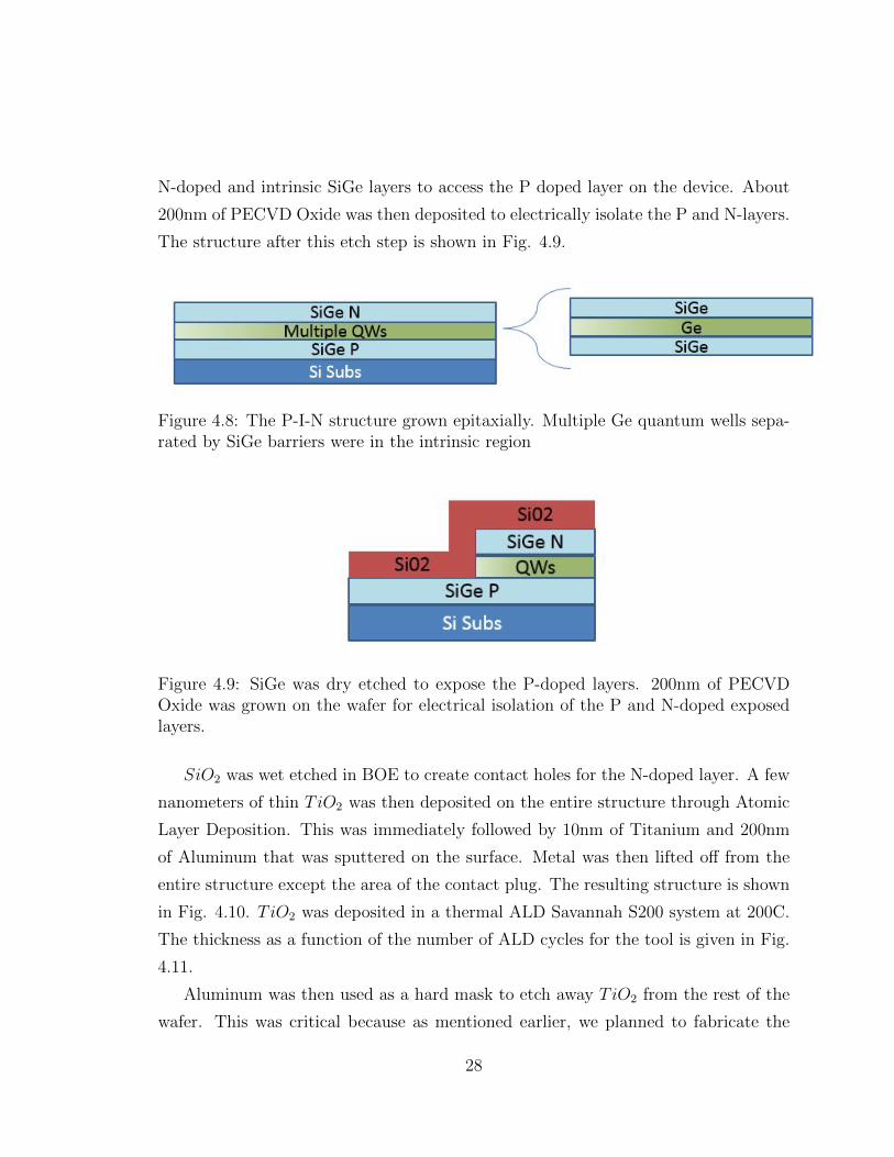
N-doped and intrinsic SiGe layers to access the P doped layer on the device. About
200nm of PECVD Oxide was then deposited to electrically isolate the P and N-layers.
The structure after this etch step is shown in Fig. 4.9.
Figure 4.8: The P-I-N structure grown epitaxially. Multiple Ge quantum wells sepa-rated by SiGe barriers were in the intrinsic region
Figure 4.9: SiGe was dry etched to expose the P-doped layers. 200nm of PECVDOxide was grown on the wafer for electrical isolation of the P and N-doped exposedlayers.
SiO2 was wet etched in BOE to create contact holes for the N-doped layer. A few
nanometers of thin TiO2 was then deposited on the entire structure through Atomic
Layer Deposition. This was immediately followed by 10nm of Titanium and 200nm
of Aluminum that was sputtered on the surface. Metal was then lifted off from the
entire structure except the area of the contact plug. The resulting structure is shown
in Fig. 4.10. TiO2 was deposited in a thermal ALD Savannah S200 system at 200C.
The thickness as a function of the number of ALD cycles for the tool is given in Fig.
4.11.
Aluminum was then used as a hard mask to etch away TiO2 from the rest of the
wafer. This was critical because as mentioned earlier, we planned to fabricate the
28

CHAPTER 4. EXPERIMENTS AND RESULTS 29
Figure 4.10: Contact plugs were etched for the N-layer. TiO2, Ti and Al were de-posited.
Figure 4.11: TiO2 deposition thickness as a function of the number of cycles onSavannah S200 Thermal ALD system

P-contacts without TiO2. Furthermore, the presence of TiO2 across the wafers might
have also caused shorts. TiO2 was dry etched from the rest of the wafer in a O2 and
CHF3 ambient. The flow rate for O2 and CHF3 was 2sccm and 15 sccm respectively.
The chamber pressure was 12.5 mT and 100 W of RF was used. TiO2 etch rate was
about 12nm/min. This etch resulted in the structure shown in Fig. 4.12.
Figure 4.12: The structure after etching TiO2 by using Al as a hard mask.
Contact plugs were then wet etched in BOE for the P-layer contacts. Ti and Al
were then sputtered and lifted off from everywhere except the contact hole. This
resulted in the final SiGe modulator structure that was shown in Fig. 4.7
4.2.3 Results and Discussion
The IV measurements of a Al/T i/N+ SiGe junction, with a sheet resistivity of 2 ∗10−3Ωcm, before and after the insertion of 7nm of TiO2, between Ti and SiGe, is
shown in Fig. 4.13. Without TiO2, the curvature of the IV curve is much larger and
IV curve resembles that of a Schottky Barrier curve. However, upon the insertion
of TiO2, the curve becomes much more linear and Ohmic in nature, thus indicating
depinning of the Fermi level.
30

CHAPTER 4. EXPERIMENTS AND RESULTS 31
Figure 4.13: IV curve of a Metal/N doped SiGe junction before and after the insertionof TiO2 between the metal and semiconductor layers.
We also investigated the optimal thickness of TiO2 to get the lowest contact
resistivity. For a device with an N doping of 7e18 cm−3, contact resistivity as a
function of TiO2 thickness is shown in Fig. 4.14. We achieved the lowest contact
resistivity at 2e-4 Ωcm2 for a TiO2 thickness of about 7nm. This is a nearly two
order of magnitude and a 25x improvement from the contact resistivity in the pinned
device.
As evident in Fig. 4.14, the contact resistivity decreases until a certain thickness of
TiO2, 7nm in our structures, is reached and then starts to increase again. The tradeoff
between a decreasing thermionic barrier and an increasing tunneling barrier has been

extensively discussed before in Chapter 2. However, this effect is not responsible
for the observed behavior because of negligable conduction band offset. Instead,
increased series resistance because of TiO2 is the source of this behavior [36]. It is
also pertinent to mention that Jason Lin et al. also achieved the minimum contact
resistivity at about 7.1nm of TiO2 thickness in Ge structures [36].
Figure 4.14: Contact Resistivity as a function of TiO2 thickness for devices with anN layer doping of 7e18 cm−3
Since the TiO2 MIS technique was originally designed for Germanium structures
by Lin, et al., it is critical to compare their improvement with what we achieved. For
a moderately doped N+ contact with a doping concentration of 1e18 cm−3, Lin, et al.,
achieved about 3 orders of magnitude reduction in the contact resistivity. Further-
more, for heavily doped N+ contacts with a doping concentration of 1e20 cm−3, Lin,
et al., managed to reduce the contact resistivty by about 2 orders of magnitude [37].
Compared to these doping concentrations, the doping concentration of our structures
of 7e18 cm−3 was between the two concentrations discussed above. One might thus
conclude that compared to Germanium, the two orders of magnitude reduction in the
contact resistivity of moderately doped Si0.20Ge0.80 N-contact through the use of this
32

CHAPTER 4. EXPERIMENTS AND RESULTS 33
MIS technique is relatively smaller. Even so, Fig. 4.13 does seem to indicate that we
almost completely depinned the Fermi level and thus were successful in minizing the
contact resistivity while preserving the functionality of our PIN modulator device.

Chapter 5
Conclusions
5.1 Summary
The primary purpose of this project was to reduce the contact resistivity in Ge-
rich Si0.20Ge0.80 modulator structures for optical interconnects. In this thesis, we
investigated two possible means of achieving this objective: A Dopant Segregation
technique and the Metal-Insulator-Semiconductor approach.
We first attempted to reduce contact resistivity, ρc, through the dopant segregation
technique and used our existing design of Al/Ti/Si0.20Ge0.80 stack. We annealed our
samples for 30s at different temperatures and characterized its impact on ρc. We found
that ρc increased for anneals performed at temperatures lower than 500C. Annealing
at higher temperatures caused shorts between the P and N layers, and we attributed
this to the diffusion of Aluminum or the thickness of the newly formed TiGe2 layer.
Germanium’s lower melting point complicated our efforts to use the mechanisms that
were already developed to depin the Fermi level in Si devices through the use of
Silicides.
We then used the MIS approach, and used TiO2 to de-pin the Fermi Level. In-
sertion of a thin layer of TiO2 between the metal and the semiconductor reduced the
penetration of metal electron wavefunction. This, in turn, lead to a reduction in the
Metal Induced Gap States (MIGS) and thus depinned the Fermi Level. We designed
and developed a new process flow to fabricate our Si0.20Ge0.80 modulator structures
34

CHAPTER 5. CONCLUSIONS 35
with a TiO2 layer between the metal and semiconductor. Using this technique, we
were able to reduce the contact resistivity of 8e18 cm−3 N-doped Si0.20Ge0.80 by 25x
and approximately two orders of magnitude. The IV curve of the contacts indicate
an almost complete depinning. This was all achieved without compromising the per-
formance of our Si0.20Ge0.80 modulator device.
5.2 Future Work
For the dopant segregation technique, Silicon saturated Aluminum can be used along
with Titanium to form the contacts. This would eliminate the possibility of Alu-
minum diffusing through the entire structure. Furthermore, instead of TiGe2, Nickel
Germanide can be explored for its possibilities of reducing the contact resistivity in
SiGe structures.
For the TiO2 MIS approach, more data points can be collected, especially between
the 6nm and 8nm thickness. Furthermore, investigations leading to establishing a
relation between doping concentration and the minimum contact resistivity would be
very interesting.
It would also be beneficial to measure the overall improvement in the RC delay
and the high frequency performance of the modulator because of the depinned Fermi
level as this is the real critical limitation for modulator performance.
Bibliography
[1] S. I. Association, “International technology roadmap for semiconductor,” 2005.
[2] C. Fan, B. Mansoorian, D. A. Van Blerkom, M. W. Hansen, V. H. Ozguz, S. C.
Esener, and G. C. Marsden, “Digital free-space optical interconnections: a com-
parison of transmitter technologies,” Applied Optics, vol. 34, no. 17, pp. 3103–
3115, 1995.
[3] E. Fei, Y. Huo, X. Chen, K. a. J. T. I. Zang, and J. S. Harris, “Ge QW waveguide
modulator.” Presented at the quarterly APIC review, 2013.
[4] Y.-H. Kuo, Y. K. Lee, Y. Ge, S. Ren, J. E. Roth, T. I. Kamins, D. A. Miller, and
J. S. Harris, “Strong quantum-confined Stark effect in Germanium quantum-well
structures on Silicon,” Nature, vol. 437, no. 7063, pp. 1334–1336, 2005.
[5] L. Brillson, “Metal-semiconductor interfaces,” Surface science, vol. 299, pp. 909–
927, 1994.
[6] Z. Zhang, Z. Qiu, R. Liu, M. Ostling, and S.-L. Zhang, “Schottky-barrier height
tuning by means of ion implantation into preformed silicide films followed by
drive-in anneal,” IEEE Electron Device Letters, vol. 28, no. 7, pp. 565–568, 2007.
[7] M. Mueller, Q. Zhao, C. Urban, C. Sandow, D. Buca, S. Lenk, S. Estevez, and
S. Mantl, “Schottky-barrier height tuning of NiGe/n-Ge contacts using as and p
segregation,” Materials Science and Engineering: B, vol. 154, pp. 168–171, 2008.
36
BIBLIOGRAPHY 37
[8] S. Zaima, O. Nakatsuka, A. Sakai, J. Murota, and Y. Yasuda, “Interfacial reac-
tion and electrical properties in Ni/Si and Ni/SiGe (c) contacts,” Applied Surface
Science, vol. 224, no. 1, pp. 215–221, 2004.
[9] J. Kojima, S. Zaima, H. Shinoda, H. Iwano, H. Ikeda, and Y. Yasuda, “Interfacial
reactions and electrical characteristics in Ti/SiGe/Si (100) contact systems,”
Applied Surface Science, vol. 117, pp. 317–320, 1997.
[10] D. Connelly, C. Faulkner, D. Grupp, and J. Harris, “A new route to zero-barrier
metal source/drain MOSFETs,” IEEE Transactions on Nanotechnology, vol. 3,
no. 1, pp. 98–104, 2004.
[11] J. Lin, “Low Resistance Contacts to N-Type Germanium,” Ph.D. dissertation,
Stanford University, 2013.
[12] E. Tasyurek, “Metal Contacts to SiGe,” Ph.D. dissertation, Stanford University,
2008.
[13] K. Saraswat, “CMOS-LOCOS EE410 instruction manual,” 2013.
[14] D. Levy, J. Ponpon, A. Grob, J. Grob, and R. Stuck, “Rapid thermal annealing
and titanium silicide formation,” Applied Physics A, vol. 38, no. 1, pp. 23–29,
1985.
[15] G. Moore, “Cramming more components onto integrated circuits,” Electronics,
28 (8), 1965.
[16] R. E. Camacho-Aguilera, Y. Cai, N. Patel, J. T. Bessette, M. Romagnoli,
L. C. Kimerling, and J. Michel, “An electrically pumped Germanium laser,”
Opt. Express, vol. 20, no. 10, pp. 11 316–11 320, May 2012. [Online]. Available:
http://www.opticsexpress.org/abstract.cfm?URI=oe-20-10-11316
[17] D. A. B. Miller, “Device requirements for optical interconnects to silicon chips,”
Proc. IEEE, vol. 97, pp. 1165 – 1185, 2009.
[18] J. Roth, O. Fidaner, E. Edwards, R. Schaevitz, Y.-H. Kuo, N. Helman,
T. Kamins, J. Harris, and D. Miller, “C-band side-entry Ge quantum-well elec-
troabsorption modulator on SOI operating at 1 V swing,” Electronics Letters,
vol. 44, no. 1, pp. 49–50, 2008.
[19] D. Englund, B. Ellis, E. Edwards, T. Sarmiento, J. S. Harris, D. A. Miller, and
J. Vuckovic, “Electrically controlled modulation in a photonic crystal nanocav-
ity,” Optics Express, vol. 17, no. 18, pp. 15 409–15 419, 2009.
[20] S. Zaima, N. Wakai, T. Yamauchi, and Y. Yasuda, “Interfacial solid-phase re-
actions, crystallographic structures, and electrical characteristics of Hf/(001) Si
systems,” Journal of applied physics, vol. 74, no. 11, pp. 6703–6709, 1993.
[21] R. F. Pierret et al., “Semiconductor device fundamentals,” 1996.
[22] W. Spicer, T. Kendelewicz, N. Newman, K. Chin, and I. Lindau, “The mecha-
nisms of Schottky barrier pinning in III–V semiconductors: Criteria developed
from microscopic (atomic level) and macroscopic experiments,” Surface Science,
vol. 168, no. 1, pp. 240–259, 1986.
[23] J. Tersoff, “Schottky barrier heights and the continuum of gap states,” Physical
Review Letters, vol. 52, no. 6, pp. 465–468, 1984.
[24] W. Monch, “Chemical trends of barrier heights in metal-semiconductor contacts:
on the theory of the slope parameter,” Applied Surface Science, vol. 92, pp. 367–
371, 1996.
[25] T. Nishimura, K. Kita, and A. Toriumi, “Evidence for strong Fermi-level pinning
due to metal-induced gap states at metal/germanium interface,” Applied Physics
Letters, vol. 91, no. 12, p. 123123, 2007.
[26] A. Dimoulas, P. Tsipas, A. Sotiropoulos, and E. Evangelou, “Fermi-level pinning
and charge neutrality level in germanium,” Applied Physics Letters, vol. 89,
no. 25, pp. 252 110–252 110, 2006.
38

BIBLIOGRAPHY 39
[27] W. Monch, “Barrier heights of real Schottky contacts explained by metal-induced
gap states and lateral inhomogeneities,” Journal of Vacuum Science & Technol-
ogy B, vol. 17, no. 4, pp. 1867–1876, 1999.
[28] S. Kurtin, T. McGill, and C. Mead, “Fundamental transition in the electronic
nature of solids,” Physical Review Letters, vol. 22, no. 26, pp. 1433–1436, 1969.
[29] G. Thareja, J. Liang, S. Chopra, B. Adams, N. Patil, S. Cheng, A. Nainani, E. Ta-
syurek, Y. Kim, S. Moffatt et al., “High performance germanium n-MOSFET
with antimony dopant activation beyond 1× 1020 cm−3,” IEDM Tech. Dig, pp.
245–248, 2010.
[30] K. Martens, A. Firrincieli, R. Rooyackers, B. Vincent, R. Loo, S. Locorotondo,
E. Rosseel, T. Vandeweyer, G. Hellings, B. De Jaeger et al., “Record low contact
resistivity to n-type Ge for CMOS and memory applications,” in Electron Devices
Meeting (IEDM), 2010 IEEE International. IEEE, 2010, pp. 18–4.
[31] S. Gannavaram, N. Pesovic, and C. Ozturk, “Low temperature (800/circc) re-
cessed junction selective silicon-germanium source/drain technology for sub-70
nm CMOS,” in Electron Devices Meeting, 2000. IEDM’00. Technical Digest. In-
ternational. IEEE, 2000, pp. 437–440.
[32] H. B. Zhao, K. L. Pey, W. K. Choi, S. Chattopadhyay, E. Fitzgerald, D. Anto-
niadis, and P. Lee, “Interfacial reactions of ni on Si1−xGex (x=0.2, 0.3) at low
temperature by rapid thermal annealing,” Journal of Applied Physics, vol. 92,
no. 1, pp. 214–217, Jul 2002.
[33] M. Kobayashi, A. Kinoshita, K. Saraswat, H.-S. P. Wong, and Y. Nishi,
“Fermi level depinning in metal/Ge Schottky junction for metal source/drain
Ge metal-oxide-semiconductor field-effect-transistor application,” Journal of Ap-
plied Physics, vol. 105, no. 2, p. 023702, 2009.
[34] B. E. Coss, C. Smith, W.-Y. Loh, P. Majhi, R. M. Wallace, J. Kim, and
R. Jammy, “Contact resistance reduction to FinFET source/drain using novel

dielectric dipole Schottky barrier height modulation method,” IEEE Electron
Device Letters, vol. 32, no. 7, pp. 862–864, 2011.
[35] T. Nishimura, K. Kita, and A. Toriumi, “A significant shift of Schottky barrier
heights at strongly pinned metal/germanium interface by inserting an ultra-thin
insulating film,” Applied Physics Express, vol. 1, no. 5, p. 051406, 2008.
[36] J.-Y. J. Lin, A. M. Roy, A. Nainani, Y. Sun, and K. C. Saraswat, “Increase in
current density for metal contacts to n-germanium by inserting TiO2 interfacial
layer to reduce Schottky barrier height,” Applied Physics Letters, vol. 98, no. 9,
p. 092113, 2011.
[37] J.-Y. Lin, A. M. Roy, and K. C. Saraswat, “Reduction in specific contact re-
sistivity to Ge using interfacial layer,” Electron Device Letters, IEEE, vol. 33,
no. 11, pp. 1541–1543, 2012.
40
Recommended