Radiation Damage in Silicon Particle Detectors in High Luminosity Experiments
Agnieszka Obłąkowska-Mucha
AGH UST Kraków
within the framework of
RD50 Collaboration
&
LHCb VELO Group
2nd Jagiellonian Symposium on Fundamental and Applied Subatomic PhysicsJune 3rd-11th, Kraków, Poland

Outline
09.06.2017 A.Obłąkowska-Mucha (AGH UST Kraków) 2nd Jagiellonian Symposium 2
1. Introduction.
2. The timeline of LHC and experiments.
3. Radiation induced changes in properties of the silicon tracking detectors.
4. Radiation damage in the LHCb VELO.
5. Development of new structures:
• 3D Pixels,
• HVCMOS,
• LGAD.
6. Measurement technique: TCT.
Simulation of 400 proton-proton collisions in just one 25 nsbunch crossing at the HL-LHC

HL-LHC Timeline
09.06.2017 A.Obłąkowska-Mucha (AGH UST Kraków) 2nd Jagiellonian Symposium 3
4. Two major shutdowns (LS2 & LS3) – main accelerator and detector upgrades.
1. LHC was planed for 10 years of operation (ℒ = 300 𝑓𝑏−1), i.e. till the end of Run 3 (2023).
2. It was assumed that tracking detectors will have to be replaced due to radiation damage and ageing (or new physics program).
3. Based on experience from Run I, with new technologies in mind, it’s the right time to design them NOW!
Futu
reC
ircu
lar
Co
llid
er

Experiments - Phase 1 Upgrade
09.06.2017 A.Obłąkowska-Mucha (AGH UST Kraków) 2nd Jagiellonian Symposium 4
Phase 1 Upgrade (24 months):• CMS - Pixel detector replacement,• LHCb - VELO strip detector replacement by pixels, new strip UT.
5.1. Upgrade of the silicon tracking detector.
Futu
reC
ircu
lar
Co
llid
er

Experiments - Phase 2 Upgrade
09.06.2017 A.Obłąkowska-Mucha (AGH UST Kraków) 2nd Jagiellonian Symposium 5
Phase 2 Upgrade (30 months):• LHC: new quadrupoles in the collision region, crab cavities, • CMS: new tracker, HGCAL,• ATLAS: replacement of the Inner Detector,• LHCb major detector upgrade during LS4
5.2. Upgrade of the silicon tracking detector.
Futu
reC
ircu
lar
Co
llid
er

High Level of fluence @ LHC and HL-LHC
09.06.2017 A.Obłąkowska-Mucha (AGH UST Kraków) 2nd Jagiellonian Symposium 6
1. LHC will produce collisions at a rate of about 5·109 s-1.
2. The annual dose at HL-LHC will be similar to the total dose until LS3:
• end of Run III (300 fb-1) Φ~2·1015 neq cm-2
• HL-LHC (3000 fb-1) Φ~2·1016 neq cm-2
4. The main objective for RD50 is development of radiation hard semiconductor detectors for HL-LHC.
5. The radiation hardness above 1016 neq cm-2 (while maintaining the S/N ratio > 10) is required with fast signal collection and affordable cost. Current LHC detector can operate up to fluence 1015 neq cm-2
6. Defect induced by particle radiation and their influence on detector performance are of major interest to RD50.
1fb-1 3000 fb-1

09.06.2017 A.Obłąkowska-Mucha (AGH UST Kraków) 2nd Jagiellonian Symposium 7
htt
ps:
//fc
c.w
eb.c
ern
.ch
/Pag
es/d
efau
lt.a
spx

8

The source of radiation damage
09.06.2017 A.Obłąkowska-Mucha (AGH UST Kraków) 2nd Jagiellonian Symposium 9
1. The main source of radiation is from particles produced in soft p-p interactions (neutrons, pions, protons) and secondary interactions with the detector material.
2. Non-Ionizing Energy Loss (Ek > 15 eV) of impinging particle may displace a silicon atom from the lattice.
3. Creation of defects depends on the kind of particle and its energy.
4. Displacements of silicon atoms produce vacancies and interstitials.
5. Crystal impurities interact with defects causing the change in electrical properties of detector.
[Mik
a H
uhti
nen
NIM
A 4
91
(20
02
) 1
94
]10 MeV protons 24 GeV/c protons 1 MeV neutrons
Simulation of radiation 1014 particles/cm2
Point defects + cluster defects + impurities = degradation of the detector

Radiation Damage - effects
09.06.2017 A.Obłąkowska-Mucha (AGH UST Krakow ) 2nd Jagiellonian Symposium 10
Radiation induced changes in properties and structures of the silicon tracking detectors are observed as macroscopic effects caused by microscopic defects:
Trapping (e and h) Charge Collection
Efficiency CCE
charged defects effective doping
concentration Neff,depletion voltage Vdep
generation/recombination leakage current I
M.M
oll’
sle
ctu
re
The microscopic defects accumulate over time and have a damaging impact on the sensor performance.
Constant monitoring of radiation influence on silicon sensors:
• Current - Voltage scans (IV), • Current - Temperature scans (IT),• Charge Collection Efficiency scan (CCE),• Change of effective depletion voltage (VED)

The LHCb VELO
09.06.2017 A.Obłąkowska-Mucha (AGH UST Kraków) 2nd Jagiellonian Symposium 11
injection stable beams
6 cm
VErtex LOcator
• Close proximity of the beam-pipe.
Performance of the LHCb Vertex Locator, J. Instrum. 9 (2014) P09007
Sensors
• VELO consist of 42 modules (two halves).
• Modules have two (R and Phi) microstrip silicon oxygenated n+-on-n sensors (two sensons are n+-on-p).
• Sensors are 300 μm thick, strip pitches: 40-100 μm.
• Evaporative CO2 cooling system keeps sensors at -7oC.
• VELO halves are movable- the movement is steered by a precise system (accuracy of 10 μm),
• When stable beams, the silicon edge is only 8 mm from the proton beam – sensors are in harsh particle fluence .
• Operated in a secondary vacuum, separated from the LHC vacuum by 300 μm thick aluminium foil.

Particle Fluence
09.06.20167 A.Obłąkowska-Mucha (AGH UST Krakow) 12
1. VELO is currently the most exposed detector in the LHC- fluence up to 1.81014 1MeV neq/cm2,
• LHCb has collected almost 5 fb-1 until now,
• VELO is designed to cope with 10-11 fb-1 .
2. The radiation field is highly non uniform – the fluence accumulated in inner and outer part of the sensor differs by a factor of ten.
Radiation environment
1 fb-1
𝒛 [𝒄𝒎]
r[𝒄𝒎]
Flu
ence
[𝒂.𝒖.]
𝟕 𝑻𝒆𝑽 + 𝟕 𝑻𝒆𝑽
𝐹𝑙𝑢𝑘𝑎 𝐿𝐻𝐶𝑏 𝑉𝐸𝐿𝑂 𝑆𝑖𝑚𝑢𝑙𝑎𝑡𝑖𝑜𝑛Preliminary

09.06.2017 A.Obłąkowska-Mucha (AGH UST Krakow) 2nd Jagiellonian Symposium 13
Leakage Current
1. The level of leakage current reveals the amount of the radiation damage contained in a detector volume.
2. The increase in leakage current is proportional to the accumulated fluence (time, delivered luminosity) : ∆𝐼 = 𝛼 ∙ 𝜙𝑒𝑞 ∙ 𝑉, typically 2 μA per 100 pb-1
annealing constant 𝛼(20℃) = 3.99 ± 0.03 ∙ 10−17 A/cm
3. The currents of the sensors are measured as a function of time while operating at nominal conditions (depletion voltage, temperature)
• Bulk currents increases with fluence esexpected, with occasional drops due to annealing.
Run II
LS1
Run I
“Radiation Damage in the LHCb VELO”JINST 8 (2013) P08002

CCE – Effective Depleted Voltage VED
09.06.2017 A.Obłąkowska-Mucha (AGH UST Kraków) 2nd Jagiellonian Symposium 14
1. At the production, initial depletion voltage was 25-70 V.
2. Sensors in 2011-12 were biased at 150 V, currently 150-200 V (250 V for n-on-p).
250 V 200 V 150 V
4. Good agreement with Hamburg model
5. We need to increase the bias voltage to 300 V, first in the most irradiated sensors.
n-on-p
Run II HV

VED – expectations for Run II
09.06.2017 A.Obłąkowska-Mucha (AGH UST Kraków) 2nd Jagiellonian Symposium 15
1. LHCb is supposed to collect 8 fb-1 by the end of Run II, what means that the VELO sensors will accumulate maximum of 71014 1MeV neq/cm2 (most irradiated tipsof the sensor).
3. VELO sensors can be operated up to 500V.
4. During LS2 (2018-19) VELO microstrip sensors will be replaced by pixels.
Hamburg model

The first radiation concern
09.06.2017 A.Obłąkowska-Mucha (AGH UST Kraków) 2nd Jagiellonian Symposium 16
The LHCb silicon vertex detector will not be replaced.The main VELO upgrade (pixels) is planned for LS2 (2018).
VELO replacement is currentlyon display at LHCb Pit.
The new innermost layer of ATLAS Inner Tracker was installed (IBL) inside the Pixel Detector during LS1.

Call RD50 in case of radiation damage problem…
09.06.2017 A.Obłąkowska-Mucha (AGH UST Kraków) 2nd Jagiellonian Symposium 17
RD50 - Radiation hard semiconductor devices for very high luminosity colliders.
1. Formed in 2001, approved by CERN in 2002.2. The main objective is:
Development of radiation hard semiconductor detectors for the luminosity upgrade of the LHC to 7.5·1034 cm-2s-1.
3. Challenges:• radiation hardness up to 1016 cm-2 required, • fast signal collection – plan for 10 ns bunch crossing, • low mass to reduce multiple scattering close to interaction point,• affordable cost.
4. The current activities od RD50 include:a) identifying the defects through dedicated measurement techniques (DLTS, TSC, TCT)
or monitoring the macroscopic changes in HEP experiments.b) work out how to get rid of damage (or avoid it) – new technologies, new structures
(3D sensors, HV CMOS, LGAD, simulation (FLUKA, GEANT4, TCAD…).c) test the solution:
• neutron exposition in nuclear reactor, • proton irradiation at cyclotrons and synchrotrons,• new dedicated irradiation center @ CERN.
d) incorporate the feedback from experiments.

Advanced detector design – 3D pixel sensors
09.06.2017 A.Obłąkowska-Mucha (AGH UST Kraków) 2nd Jagiellonian Symposium 18
1. Currently a well known technology (S.I. Parker et al., NIMA 395(1997)328).
2. 3D pixel sensors are installed in ATLAS IBL, AFP, CMS Totem.
3. They are designed as vertical narrow columnar p and n electrodespenetrating the silicon substrate.
3D pixels
3. Advantages:• diameter: 10 mm, distance L: 50 – 100 mm (small drift
distance, less trapping),• lower depletion voltage: 10-200V (lower power),
thinner detectors possible,• fast signal formation,• radiation hard,• active or slim edges technology.
4. Problems:• Non uniform spatial response (electrodes are inefficient regions).• Higher capacitance, higher noise.• Complicated fabrication technology (bump-bonding, time, cost, yield).
3D Pixels /Strips
Planar pixels
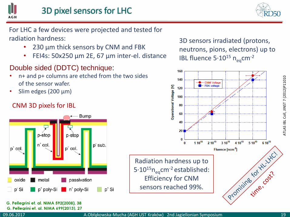
3D pixel sensors for LHC
09.06.2017 A.Obłąkowska-Mucha (AGH UST Kraków) 2nd Jagiellonian Symposium 19
For LHC a few devices were projected and tested for radiation hardness:
• 230 μm thick sensors by CNM and FBK • FEI4s: 50x250 μm 2E, 67 μm inter-el. distance
CNM 3D pixels for IBL
Double sided (DDTC) technique:• n+ and p+ columns are etched from the two sides
of the sensor wafer.• Slim edges (200 μm)
3D sensors irradiated (protons, neutrons, pions, electrons) up to IBL fluence 5·1015 neqcm-2
Radiation hardness up to5·1015neqcm-2 established:
Efficiency for CNM sensors reached 99%.
ATL
AS
IBL
Co
ll, J
INST
7 (
20
12
)P1
10
10

3D pixel sensors for HL-LHC - prospects
09.06.2017 A.Obłąkowska-Mucha (AGH UST Kraków) 2nd Jagiellonian Symposium 20
The signal efficiency is about 60-70% at 5·1015 neqcm-2 and 30% at almost 1016 neqcm-2 with not much increase of 𝑉𝑏𝑖𝑎𝑠.
Signal efficiency was improved with decreasing electrode distance.
[1] ATLAS IBL Collaboration, submitted to JINST (2012)
[2] M. Koehler et al. NIMA 659 (2011) 272
[3] C. Da Via, et al., NIMA 604 (2009) 505
Compilation by C. Da Via
RD 50 project:Joint MPW pixel run for ATLAS, CMS, LHCb.
Motivations:1. Manufacture smaller area pixels on thin sensors.2. Study of radiation hardness.
Lop
ez P
azet
al..
RD
50
wo
rksh
op
20
15
, CER
N
New technology – HV CMOS
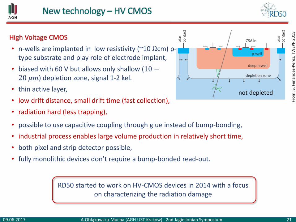
09.06.2017 A.Obłąkowska-Mucha (AGH UST Kraków) 2nd Jagiellonian Symposium 21
High Voltage CMOS
• n-wells are implanted in low resistivity (~10 Ωcm) p-type substrate and play role of electrode implant,
• biased with 60 V but allows only shallow (10 −20 𝜇𝑚) depletion zone, signal 1-2 kel.
• thin active layer,
• low drift distance, small drift time (fast collection),
• radiation hard (less trapping),
Fro
m: S
. Fen
and
ez-P
erez
, TW
EPP
20
15
not depleted
RD50 started to work on HV-CMOS devices in 2014 with a focus on characterizing the radiation damage
• possible to use capacitive coupling through glue instead of bump-bonding,
• industrial process enables large volume production in relatively short time,
• both pixel and strip detector possible,
• fully monolithic devices don’t require a bump-bonded read-out.

HV CMOS – signal collection
09.06.2017 A.Obłąkowska-Mucha (AGH UST Kraków) 2nd Jagiellonian Symposium 22
High voltage is used to deplete a part of the substrate:
• The main charge collection mechanism is drift,
• Part of the signal originates from the undepleted region and is collected by diffusion,
• Edge-TCT measurements showed drift and diffusion component
M.F
ern
ánd
ezG
arcí
aR
D5
0 W
ork
sho
p N
ov
20
14
drift
diffusion
The charge collection profiles of irradiated samples show quick disappearance of drift constituent.
HV CMOS – irradiation tests
09.06.2017 A.Obłąkowska-Mucha (AGH UST Kraków) 2nd Jagiellonian Symposium 23
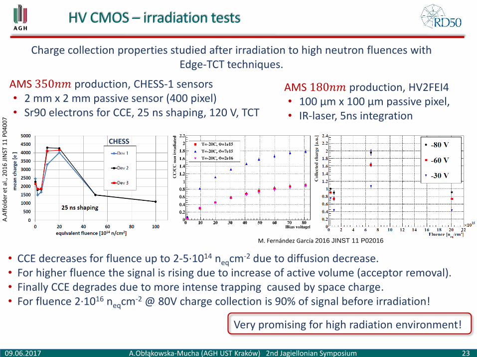
Charge collection properties studied after irradiation to high neutron fluences with Edge-TCT techniques.
AMS 350𝑛𝑚 production, CHESS-1 sensors• 2 mm x 2 mm passive sensor (400 pixel) • Sr90 electrons for CCE, 25 ns shaping, 120 V, TCT
AMS 180𝑛𝑚 production, HV2FEI4• 100 µm x 100 µm passive pixel,• IR-laser, 5ns integration
A.A
ffo
lder
et a
l., 2
01
6JI
NST
11
P0
40
07
M. Fernández García 2016 JINST 11 P02016
• CCE decreases for fluence up to 2-5·1014 neqcm-2 due to diffusion decrease.• For higher fluence the signal is rising due to increase of active volume (acceptor removal). • Finally CCE degrades due to more intense trapping caused by space charge.• For fluence 2·1016 neqcm-2 @ 80V charge collection is 90% of signal before irradiation!
Very promising for high radiation environment!
CHESS
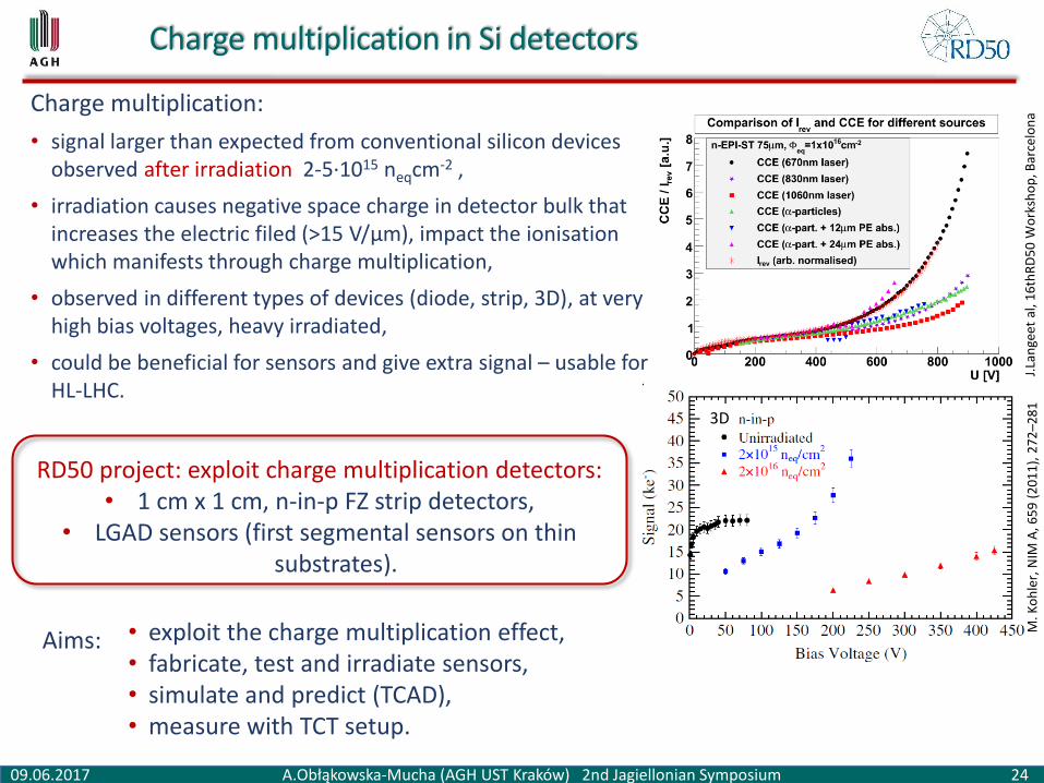
Charge multiplication in Si detectors
09.06.2017 A.Obłąkowska-Mucha (AGH UST Kraków) 2nd Jagiellonian Symposium 24
Charge multiplication:
• signal larger than expected from conventional silicon devices observed after irradiation 2-5·1015 neqcm-2 ,
• irradiation causes negative space charge in detector bulk that increases the electric filed (>15 V/μm), impact the ionisationwhich manifests through charge multiplication,
• observed in different types of devices (diode, strip, 3D), at very high bias voltages, heavy irradiated,
• could be beneficial for sensors and give extra signal – usable for HL-LHC.
RD50 project: exploit charge multiplication detectors:• 1 cm x 1 cm, n-in-p FZ strip detectors,
• LGAD sensors (first segmental sensors on thin substrates).
• exploit the charge multiplication effect, • fabricate, test and irradiate sensors,• simulate and predict (TCAD),• measure with TCT setup.
M. K
oh
ler,
NIM
A, 6
59
(2
01
1),
27
2–2
81
3D
J.La
nge
etal
, 16
thR
D5
0 W
ork
sho
p, B
arce
lon
a
Aims:

LGAD
09.06.2017 A.Obłąkowska-Mucha (AGH UST Kraków) 2nd Jagiellonian Symposium 25
The Low Gain Avalanche Detector (LGAD): a new concept of silicon radiation detector with intrinsic multiplication of the charge.
Advantages:• higher charge collection efficiency, • short drift time, • signal shorter and steeper while retaining a large amplitude
due to the multiplication mechanism.
After irradiation (reactor neutrons and 800 MeV protons):• decrease of charge collection,
G.K
ram
ber
ger
et a
l. 2
01
5 J
INST
10
P0
70
06
G.K
ram
ber
ger
RD
50
Wo
rksh
op
Ju
ne
20
14
New technology – Gallium instead of Boron or add Carbon to prevent Boron removal
• decrease of multiplication (before irradiation it was 3 times higher than standard diode), after irradiation with fluence 2·1015 neqcm-2 the gain was lost.

Measurement techniques - TCT
09.06.2017 A.Obłąkowska-Mucha (AGH UST Kraków) 2nd Jagiellonian Symposium 26
Edge Transient Charge Technique:
Method of reconstruction of electric field pioneered by Ljubljana group and promoted by RD50.
• photon pulses (below 1Hz) from an infrared laser aredirected towards the detector edge, perpendicular to the strips and focused to the region below the readout strip, electron-hole pairs are produced,
G. K
amb
erge
ret
al.
20
14
JIN
ST 9
P1
00
16
• scans across the detector thickness enables relative measurement of the induced current at given depth, extrapolate rise time, drift velocity and charge collection profiles 𝑄(𝑉𝑏𝑖𝑎𝑠),
• mobility of electrons and holes can be extracted from the drift time,
• finally, the electric field can be reconstructed by determination of drift velocity.
Edge-TCT is widely used ideal tool to study substrate properties!
𝑦𝑑𝑒𝑝𝑙

TCT- flash of results
09.06.2017 A.Obłąkowska-Mucha (AGH UST Kraków) 2nd Jagiellonian Symposium 27
HV-CMOS – different structures:• irradiated by reactor neutrons and PS protons,• charge profiles at different depth and vs. bias voltage,• width of charge collection,• determination of Neff
Results:
• neutron irradiation up to 2 × 10¹⁵ 𝑛𝑒𝑞 𝑐𝑚−2 -
increase of depletion region (initial acceptor removal), increase of space charge and charge collection• these effects are degrading with fluence
G. K
ram
ber
ger
et a
l.,2
01
6 J
INST
11
P0
40
07
AMS CHESS1 chips (20 Wcm)
Scan direction
Igo
r M
and
ić,R
D5
0 W
ork
sho
p, J
un
e 2
01
6,
Tori
no

09.06.2017 A.Obłąkowska-Mucha (AGH UST Kraków) 2nd Jagiellonian Symposium 28
TCT- 3D and LGAD example
Signal amplification in strip-LGAD
Iván
Vila
, RD
50
Wo
rksh
op
, Ju
ne
20
16
G.P
elle
grin
iRD
50
Wo
rksh
op
Dec
20
15
3D pixels (CNM) –
irradiated by reactor neutrons with 5 × 10¹⁵ 𝑛𝑒𝑞 𝑐𝑚−2

09.06.2017 A.Obłąkowska-Mucha (AGH UST Kraków) 2nd Jagiellonian Symposium 29
SUMMARY
1. Silicon detectors currently installed in LHC experiments need to be replaced by 2023 at the latest.
2. Current technologies are not sufficient to withstand fluence at the level of 1016 𝑛𝑒𝑞 𝑐𝑚
−2.
3. The new region of interest for FCC – fluence up to 1018 𝑛𝑒𝑞 𝑐𝑚−2.
4. RD50 Collaboration has been working on:• new technologies and new structures: 3D sensons, LGAD, HV-CMOS description of
defects and material characterization,• simulation of the structures and radiation effects,• methods of measurements and test of irradiated devices.
5. The monitoring of radiation damage in Vertex Locator @ LHCb showed symptoms of degradation at the level as expected.
6. Vertex Locator is performing successfully in Run II obtaining the resolutions similar to Run I.

09.06.2017 A.Obłąkowska-Mucha (AGH UST Kraków) 2nd Jagiellonian Symposium 30
SPARES

Radiation damage effects (1)
09.06.2017 A.Obłąkowska-Mucha (AGH UST Kraków) 2nd Jagiellonian Symposium 31
Radiation induced changes in properties and structures of the silicon tracking detectors are observed as ...
macroscopic effects … caused by … microscopic defects
10-1 100 101 102 103
eq [ 1012 cm-2 ]
1
510
50100
5001000
5000
Ud
ep [
V]
(d =
300m
m)
10-1
100
101
102
103
| Nef
f |
[ 10
11 c
m-3
]
600 V 600 V
1014cm-21014cm-2
"p - type""p - type"
type inversiontype inversion
n - typen - type
[Data from R. Wunstorf 92]
1. Change of depletion voltage: due to charged energy levels in the depleted region.
Defects change the effective doping concentration and has impact on bias voltage used to fully deplete the sensor. Significant progress on identifying defects was performed within RD50 group.
Due to excess of acceptor-like defects and donor removal, initially n-type sensor changes into p-type sensor (at LHC first observed in LHCb VELO).
Valence Band
Conduction Band
Appl. Phys. Lett. 82, 2169 (2003), Nucl. Instr. and Meth. in Phys. Res. A 611 (2009) 52, Appl. Phys. Lett. 92 (2008) 024101; )J.Appl.Phys. 117 (2015) 164503; Nucl. Instr. and Meth. in Phys. Res. A 612 ,525-529, 2010.

Radiation damage effects (2)
09.06.2017 A.Obłąkowska-Mucha (AGH UST Kraków) 2nd Jagiellonian Symposium 32
2. Increase of leakage current: bulk current due to
generation/recombination centers in the mid-gap.
1011 1012 1013 1014 1015
eq [cm-2]
10-6
10-5
10-4
10-3
10-2
10-1
I
/ V
[
A/c
m3]
n-type FZ - 7 to 25 KWcm
n-type FZ - 7 KWcm
n-type FZ - 4 KWcm
n-type FZ - 3 KWcm
n-type FZ - 780 Wcm
n-type FZ - 410 Wcm
n-type FZ - 130 Wcm
n-type FZ - 110 Wcm
n-type CZ - 140 Wcm
p-type EPI - 2 and 4 KWcm
p-type EPI - 380 Wcm
[M.Moll PhD Thesis][M.Moll PhD Thesis]
Valence Band
Conduction Band
holes
electrons
Radiation induced changes in properties and structures of the silicon tracking detectors are observed as ...
macroscopic effects … caused by … microscopic defects
Defects are able to capture and emit electrons and holes – source of the reverse-bias current.
Higher noise and power consumption.

Radiation damage effects (3)
09.06.2017 A.Obłąkowska-Mucha (AGH UST Kraków) 2nd Jagiellonian Symposium 33
3. Decrease of charge collection efficiency:
due to damage induced trapping centers.
Valence Band
Conduction Band
holes
electrons
CM
S Tr
acke
r JI
NST
9 (
20
14
)12
Radiation induced changes in properties and structures of the silicon tracking detectors are observed as ...
macroscopic effects … caused by … microscopic defects
Defects act as a trapping centers - electrons and holes are re-emitted with some time delay.
The signal charge is trapped and may be released too late for 25 ns read-out.
This is the most serious problem for detector irradiated with fluence above 1015 neqcm-2.

3. The effective depletion voltage (VED) is the voltage where MPV is 80% of maximum.
4. Type inversion occurred at (10-15)×1012
1MeV neq/cm2, inversion started at inner radius.
1. During data taking a tested sensor is excluded from the track fit.
2. A voltage bias scan is performed on it and the charge deposited in sensor around the track intercept is measured.
Charge Collection Efficiency - VED
09.06.2017 A.Obłąkowska-Mucha (AGH UST Kraków) 2nd Jagiellonian Symposium 34
Charge Collection Efficency (CCE)
CCE scan is used to measure:• Effective Depletion Voltage (VED)• Cluster Finding Efficiency (CFE)

3D pixel sensors for HL-LHC
09.06.2017 A.Obłąkowska-Mucha (AGH UST Kraków) 2nd Jagiellonian Symposium 35
Development of new generation 3D pixel sensors for HL-LHC:
• radiation hardness up to 2·1016 neqcm-2.
• reduced pixel size: 50 × 50 𝜇𝑚2 or 25 × 100 𝜇𝑚2.
• small inter-electrode distance (less trapping).
• reduced thickness 100 − 150 𝜇𝑚 (small leakage current).
First prototype of new generation 3D pixels finished (January 2016).
Three different technologies tested:
single sided, active edgedouble sided

Joint 3D MPW pixel run
09.06.2017 A.Obłąkowska-Mucha (AGH UST Kraków) 2nd Jagiellonian Symposium 36
A
B C
C
D
E
F
F
G
G
GG
GGH
L L L
M
M
N O N
IIII
II
Test of different configurations for various read out chips and pitch size:
• A: standard Fe-I4• B:25x100um2 ("25x500" 1E, with 3DGR - a la GP).• C:50x50um2 with the rest connected to GND with 3DGR• D:25x100um2 (2E - version 4x100+grid to GND - a la GF)• E:50x50um2 with the rest connected to GND without 3DGR• F:FEI3 device: x 50x50um2 with rest to GND with 3D GR• G: ROC4sens 50x50um2• H: PSI46dig• I FERMILAB RD ROC 30x100um2• L: Velopix 55x55um2• M: Strip 50x50um2• M Strip 25x100um2• O Strip 30x100um2f
Joint Multi Project Wafer pixel run for ATLAS, CMS, LHCb.
G.P
elle
grin
iRD
50
Wo
rksh
op
Dec
20
15
50mm 35mm
Also single sided technology:• 50𝜇𝑚 thick detectors with SOI support
wafer (350 𝜇𝑚 ), • Possible to thin down the detectors.• 5𝜇𝑚 hole diameter.• Detector tested, good I-V,• more complicated technology

RD50 Organisation
09.06.2017 A.Obłąkowska-Mucha (AGH UST Kraków) 2nd Jagiellonian Symposium 37
RD50 - Radiation hard semiconductor devices for very high luminosity colliders
Co-SpokespersonsGianluigi Casse and Michael Moll
(Liverpool University, UK (CERN EP-DT)
& FBK-CMM, Trento, Italy)
Defect / MaterialCharacterization
Ioana Pintilie(NIMP Bucharest)
Detector CharacterizationEckhart Fretwurst(Hamburg University)
Full Detector Systems
Gregor Kramberger(Ljubljana University)
•Characterization of test structures (IV, CV, CCE, TCT,.)
•Development and testing of defect engineered silicon devices
•EPI, MCZ and other materials•NIEL (experimental)•Device modeling•Operational conditions•Common irradiations• Wafer procurement (M.Moll)•Acceptor removal (Kramberger)
• 3D detectors• Thin detectors• Cost effective solutions• Other new structures• Detectors with internal gain
(avalanche detectors)• LGAD:Low Gain Avalanche Det.• Deep depleted Avalanche Det.• Slim Edges• HVCMOS• 3D (R.Bates)• LGAD (S.Hidalgo)• Slim Edges (V.Fadeyev)
• LHC-like tests• Links to HEP(LHC upgrade, FCC)• Links electronics R&D• Low rho strips• Sensor readout (Alibava)• Comparison:
- pad-mini-full detectors- different producers
•Radiation Damage in HEP detectors
•Test beams (M.Bomben & G.Casse)
New Structures
Giulio Pellegrini (CNM Barcelona)
M.Moll September 2016
Collaboration Board Chair & Deputy: G.Kramberger (Ljubljana) & J.Vaitkus (Vilnius), Conference committee: U.Parzefall (Freiburg)CERN contact: M.Moll (EP-DT), Secretary: V.Wedlake (EP-DT), Interim budget holder & GLIMOS: M.Moll (EP-DT)
• Characterization ofmicroscopic propertiesof standard-, defect engineered and new materials pre- and post-irradiation
• DLTS, TSC, ….• SIMS, SR, …• NIEL (calculations)• Cluster and Point defects• Boron related defects
Recommended