Prof. Dan Connors
Multicore Architecture
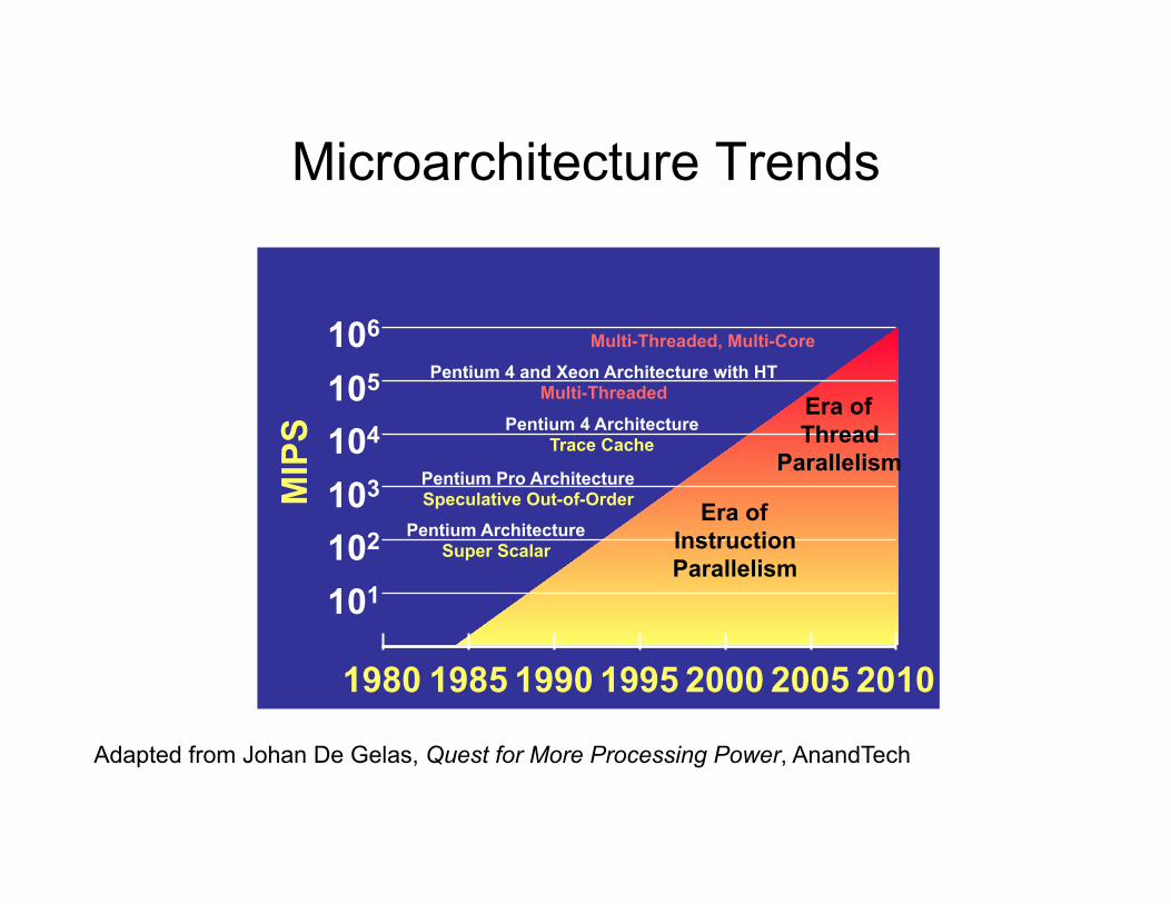
Microarchitecture Trends
Adapted from Johan De Gelas, Quest for More Processing Power, AnandTech
101 102 103 104 105 106
MIP
S
1980 1985 1990 1995 2000 2005 2010
Pentium Architecture Super Scalar
Pentium Pro Architecture Speculative Out-of-Order
Pentium 4 Architecture Trace Cache
Pentium 4 and Xeon Architecture with HT Multi-Threaded
Multi-Threaded, Multi-Core
Era of Instruction Parallelism
Era of Thread
Parallelism
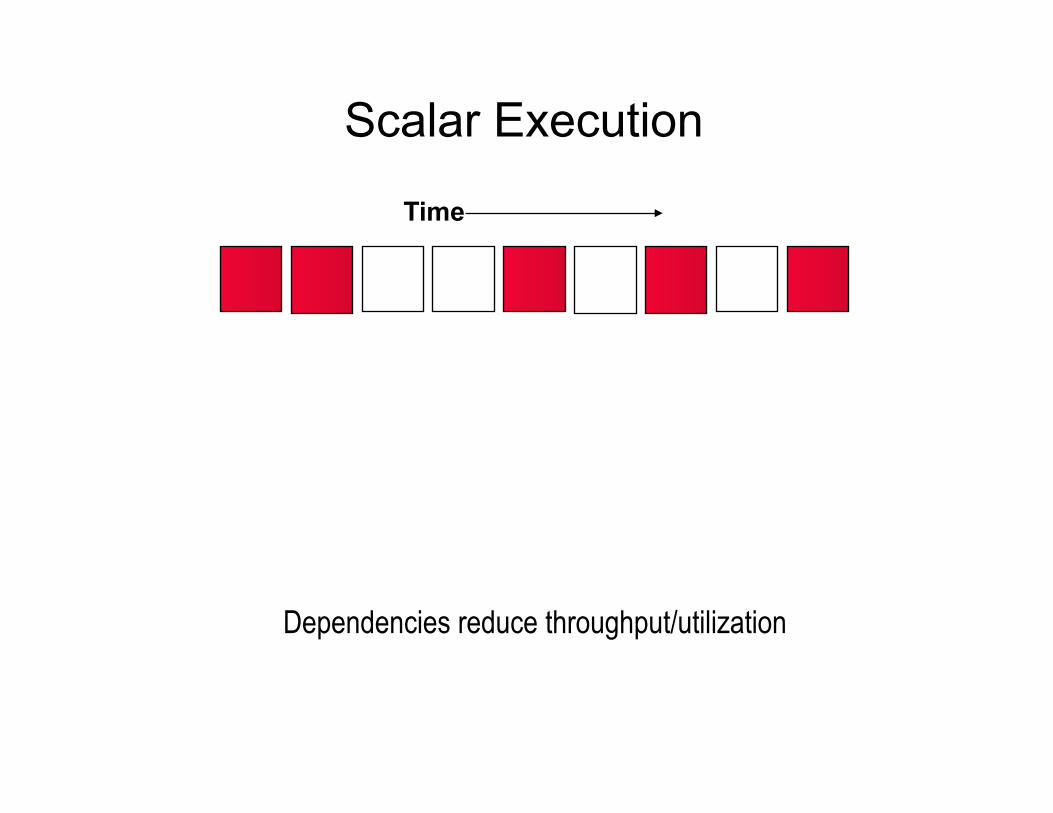
Scalar Execution
Dependencies reduce throughput/utilization
Time
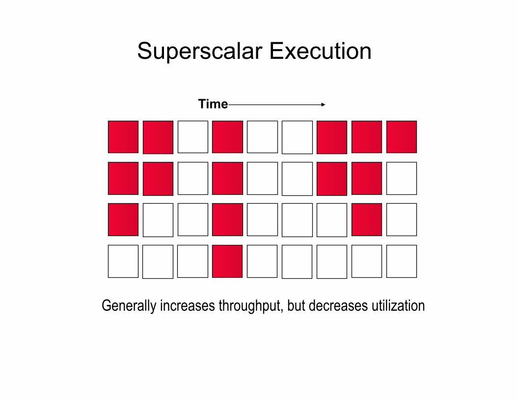
Superscalar Execution
Generally increases throughput, but decreases utilization
Time
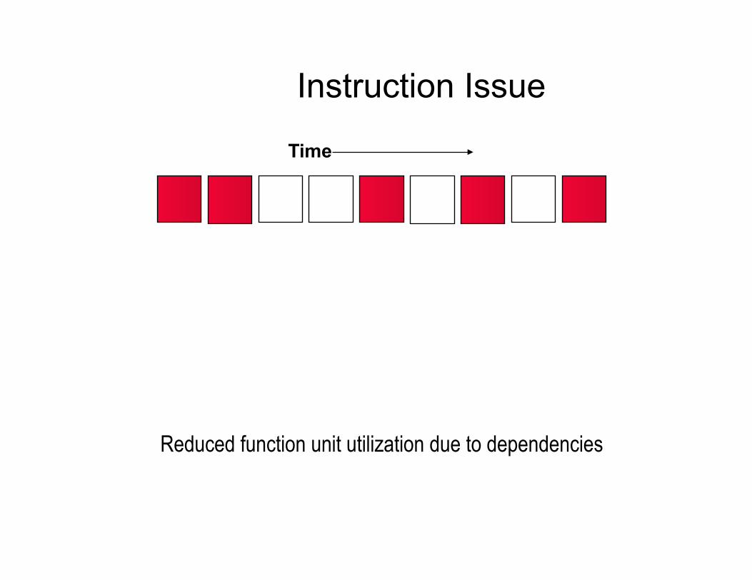
Instruction Issue
Reduced function unit utilization due to dependencies
Time
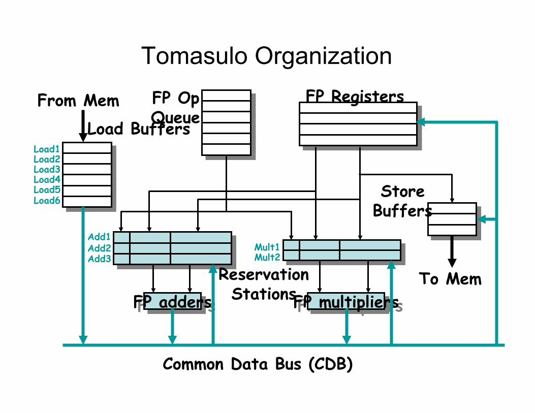
Tomasulo Organization
FP adders
Add1 Add2 Add3
FP multipliers
Mult1 Mult2
From Mem FP Registers
Reservation Stations
Common Data Bus (CDB)
To Mem
FP Op Queue Load Buffers
Store Buffers
Load1 Load2 Load3 Load4 Load5 Load6
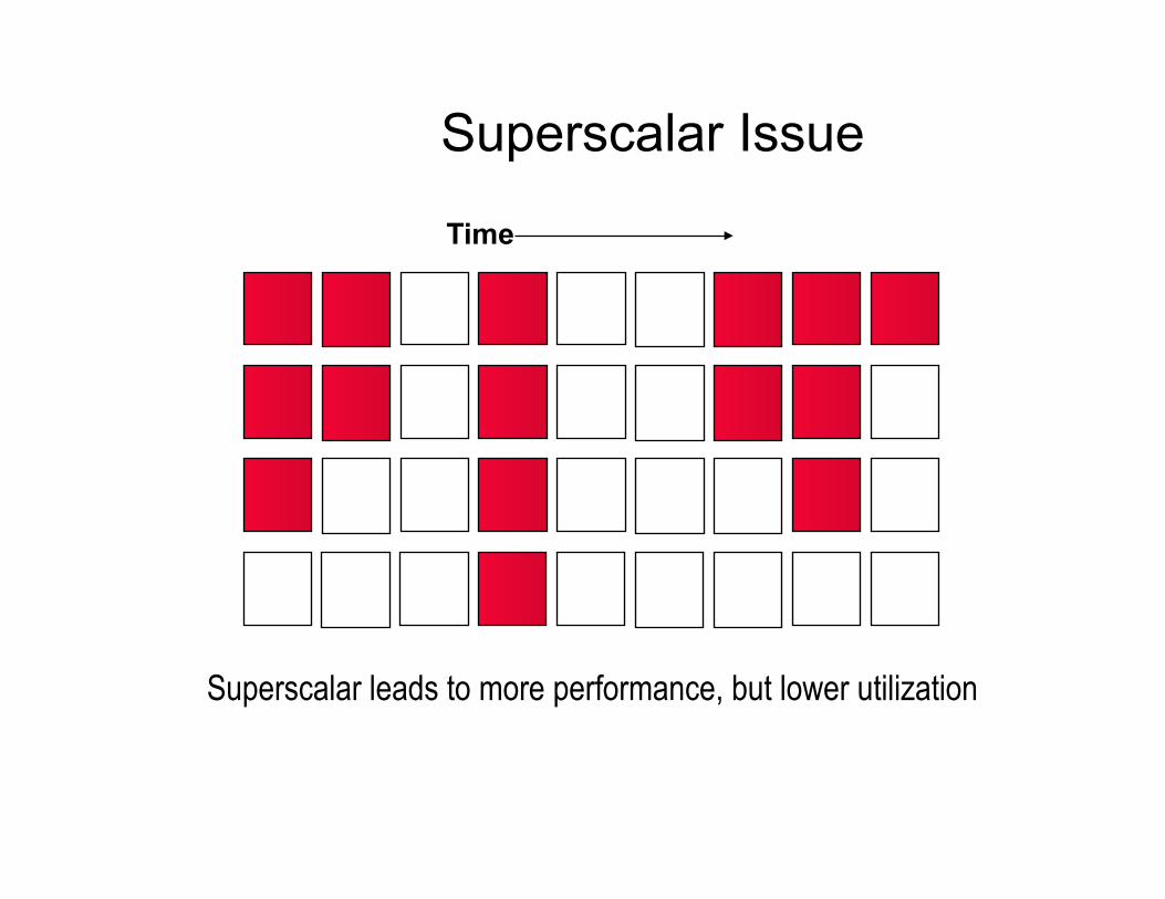
Superscalar Issue
Superscalar leads to more performance, but lower utilization
Time
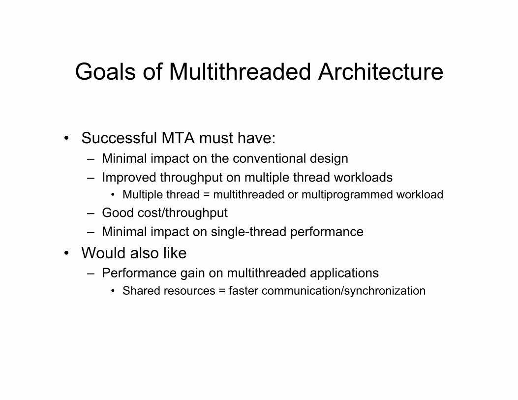
Goals of Multithreaded Architecture
• Successful MTA must have: – Minimal impact on the conventional design – Improved throughput on multiple thread workloads
• Multiple thread = multithreaded or multiprogrammed workload – Good cost/throughput – Minimal impact on single-thread performance
• Would also like – Performance gain on multithreaded applications
• Shared resources = faster communication/synchronization
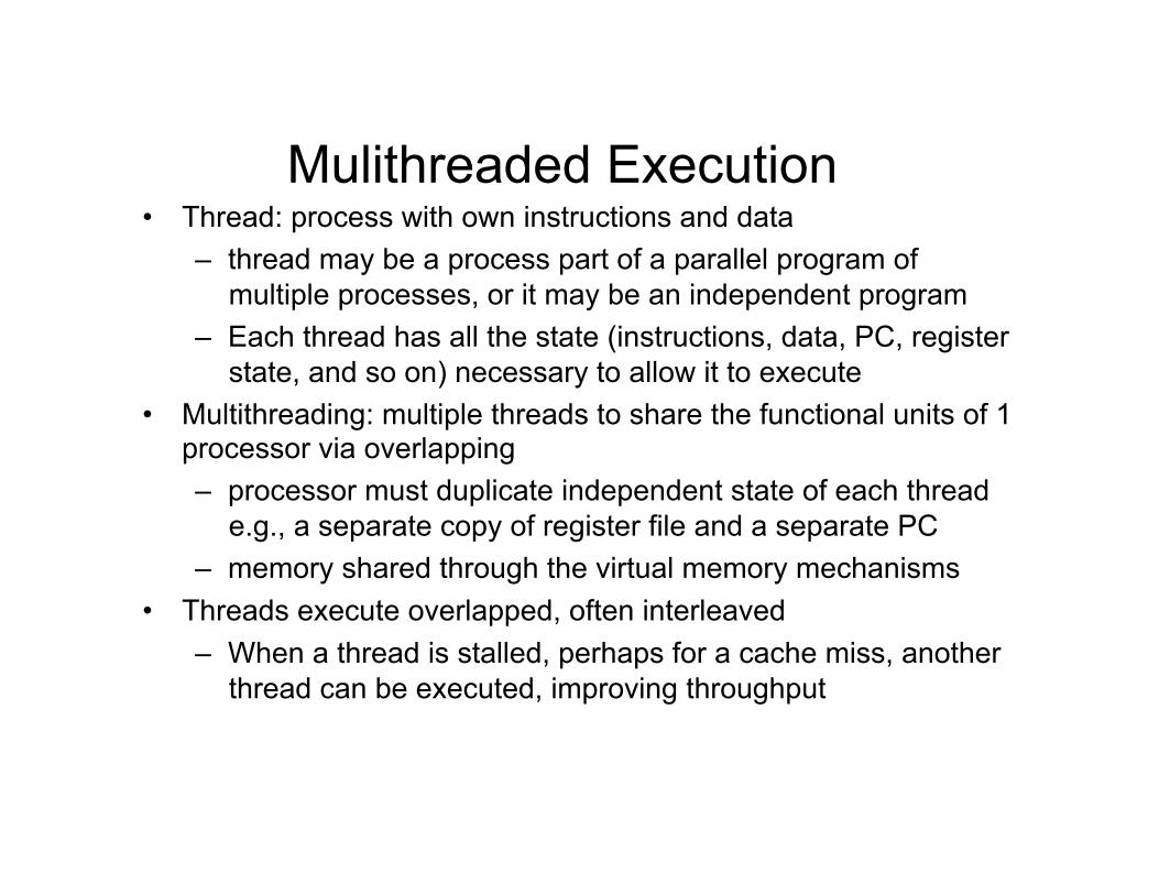
Mulithreaded Execution • Thread: process with own instructions and data
– thread may be a process part of a parallel program of multiple processes, or it may be an independent program
– Each thread has all the state (instructions, data, PC, register state, and so on) necessary to allow it to execute
• Multithreading: multiple threads to share the functional units of 1 processor via overlapping – processor must duplicate independent state of each thread
e.g., a separate copy of register file and a separate PC – memory shared through the virtual memory mechanisms
• Threads execute overlapped, often interleaved – When a thread is stalled, perhaps for a cache miss, another
thread can be executed, improving throughput
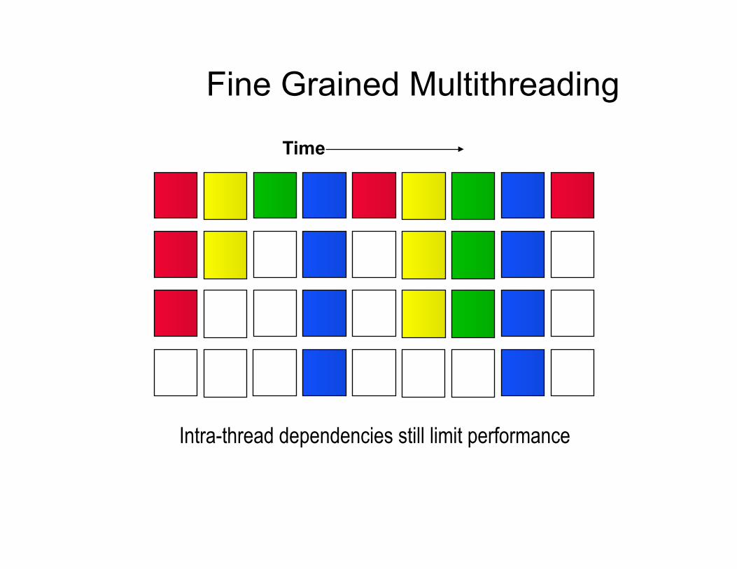
Fine Grained Multithreading
Intra-thread dependencies still limit performance
Time
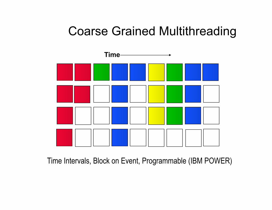
Coarse Grained Multithreading
Time Intervals, Block on Event, Programmable (IBM POWER)
Time
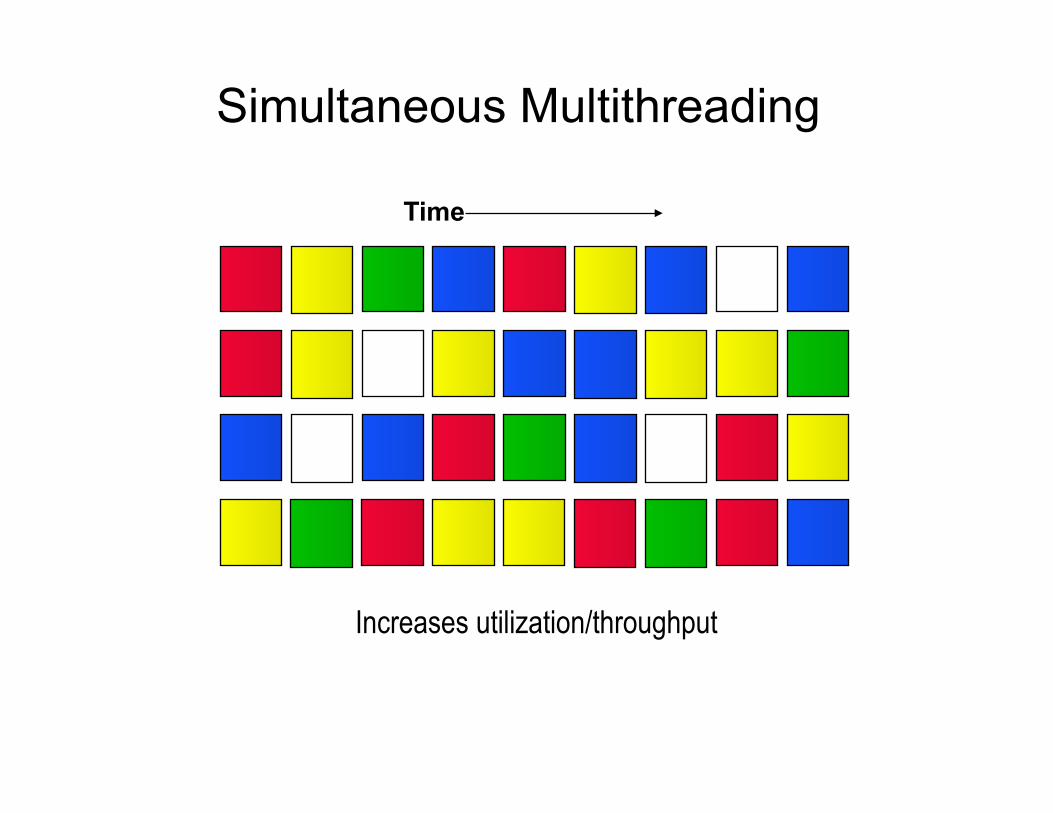
Simultaneous Multithreading
Increases utilization/throughput
Time
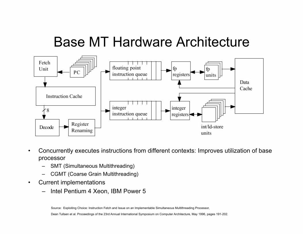
Base MT Hardware Architecture
Source: Exploiting Choice: Instruction Fetch and Issue on an Implementable Simultaneous Multithreading Processor,
Dean Tullsen et al. Proceedings of the 23rd Annual International Symposium on Computer Architecture, May 1996, pages 191-202.
• Concurrently executes instructions from different contexts: Improves utilization of base processor
– SMT (Simultaneous Multithreading) – CGMT (Coarse Grain Multithreading)
• Current implementations – Intel Pentium 4 Xeon, IBM Power 5
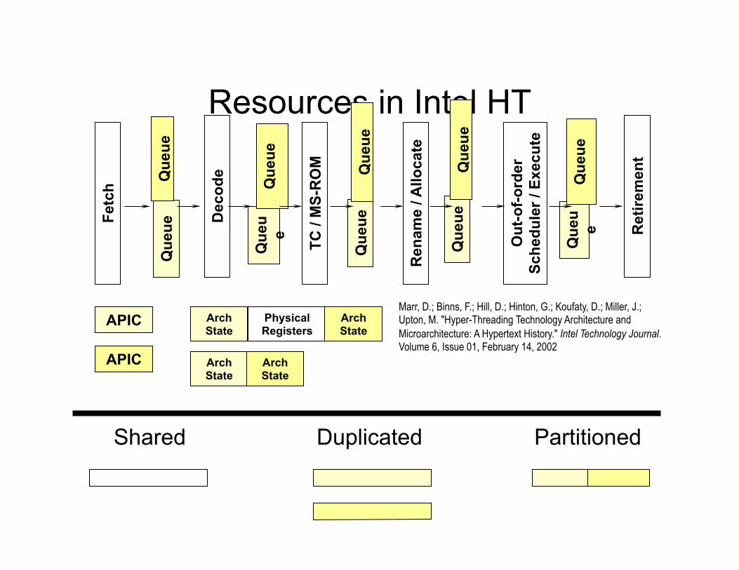
Resources in Intel HT Fe
tch
Dec
ode
Que
ue
Que
ue
TC /
MS-
RO
M
Que
ue
Que
ue
Ren
ame
/ Allo
cate
Que
ue
Que
ue
Out
-of-o
rder
Sc
hedu
ler /
Exe
cute
Ret
irem
ent
Que
ue
Que
ue
Arch State
Arch State
Arch State
Physical Registers
Arch State
APIC
APIC
Marr, D.; Binns, F.; Hill, D.; Hinton, G.; Koufaty, D.; Miller, J.; Upton, M. "Hyper-Threading Technology Architecture and Microarchitecture: A Hypertext History." Intel Technology Journal. Volume 6, Issue 01, February 14, 2002
Shared Duplicated Partitioned
Que
ue
Que
ue
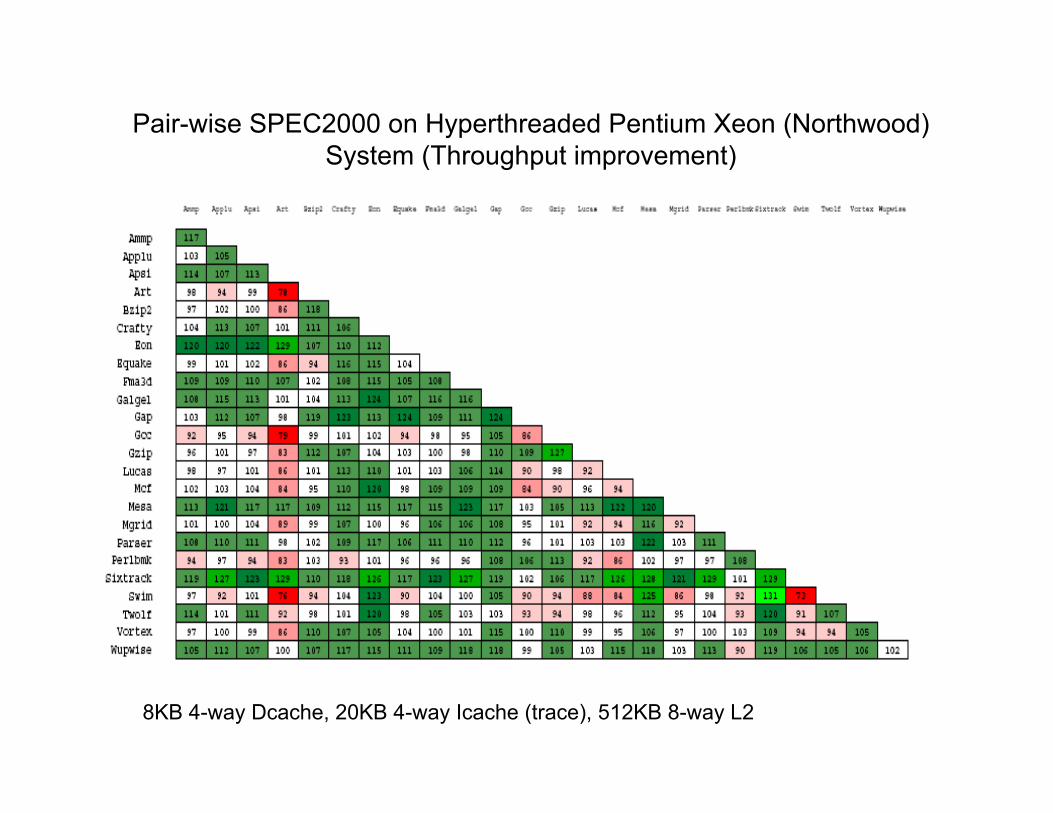
Pair-wise SPEC2000 on Hyperthreaded Pentium Xeon (Northwood) System (Throughput improvement)
8KB 4-way Dcache, 20KB 4-way Icache (trace), 512KB 8-way L2
Offline Consideration
• Read the following IEEE Micro article – SINGLE-THREADED VS. MULTITHREADED: WHERE SHOULD WE
FOCUS? • http://www.cs.wisc.edu/multifacet/papers/ieeemicro07_debate.pdf
• OR watch the video – Single-Threaded vs. Multi-Threaded
• http://www.ele.uri.edu/CARD/summary.html
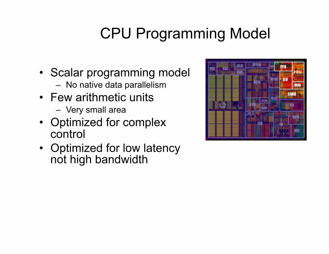
CPU Programming Model
• Scalar programming model – No native data parallelism
• Few arithmetic units – Very small area
• Optimized for complex control
• Optimized for low latency not high bandwidth
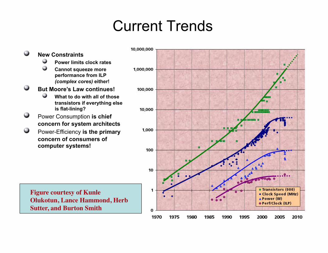
Current Trends
" New Constraints " Power limits clock rates " Cannot squeeze more
performance from ILP (complex cores) either!
" But Moore’s Law continues! " What to do with all of those
transistors if everything else is flat-lining?
" Power Consumption is chief concern for system architects
" Power-Efficiency is the primary concern of consumers of computer systems!!
Figure courtesy of Kunle Olukotun, Lance Hammond, Herb Sutter, and Burton Smith
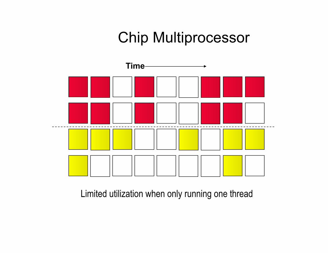
Chip Multiprocessor
Limited utilization when only running one thread
Time
Content Copyright IEEE 2009 extracted from ISSCC 2009
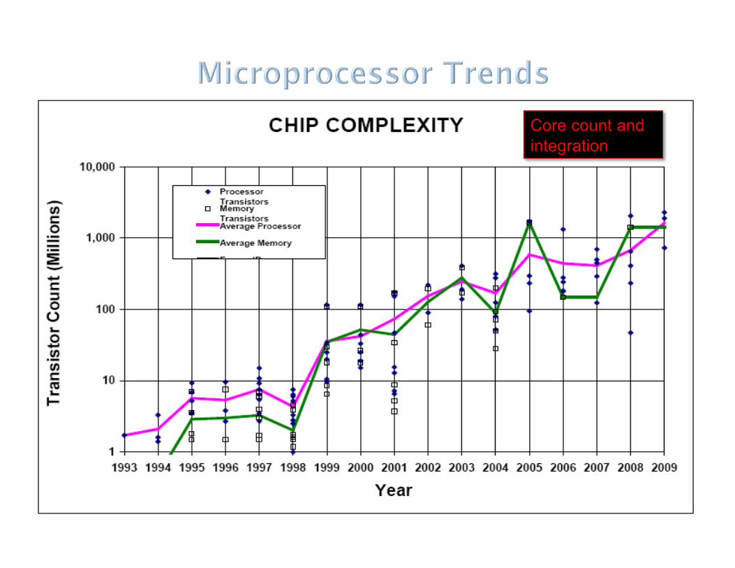
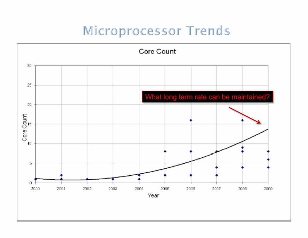
Core count and integration
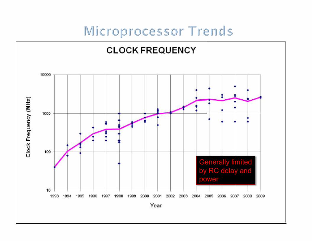
Generally limited by RC delay and power
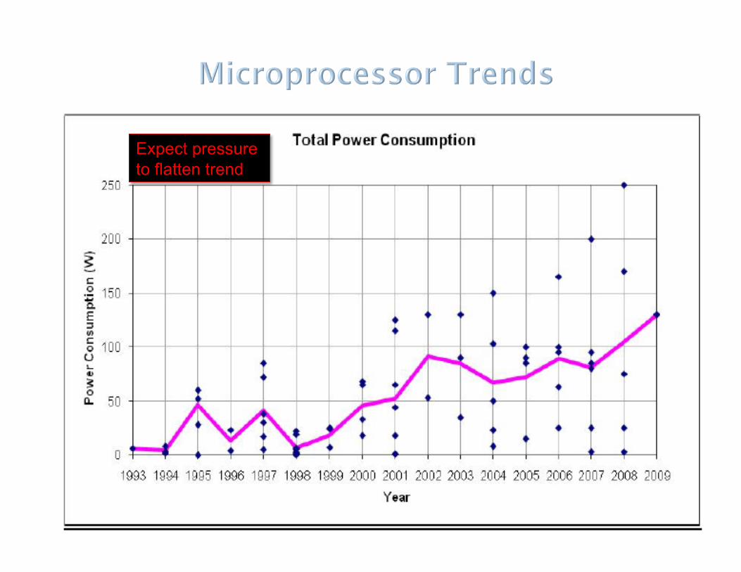
Expect pressure to flatten trend
Content Copyright IEEE 2009 extracted from ISSCC 2009
What long term rate can be maintained?

Generalized Multicore
• Cache hierarchy (shared or split) for multicores
• Cache partitioning and replacement policies have been active research

Architecture of Multicore Chips • High-performance CPUs were pushing clock
frequency faster than technology scaling allowed – Power was going up, design technique was to lower voltage – Can’t lower voltage anymore due to leakage current – Reducing Vdd requires reducing Vth, which raises
subthreshold leakage – Can’t reduce Vdd and the processor becomes power limited
due to thermal constraints... – Replicate cores to track technology scaling!

Architecture of Dual-Core Chips • IBM Power5
– Shared 1.92 Mbyte L2 cache • AMD Opteron
• Intel Pentium 4 – “Glued” two processors
together
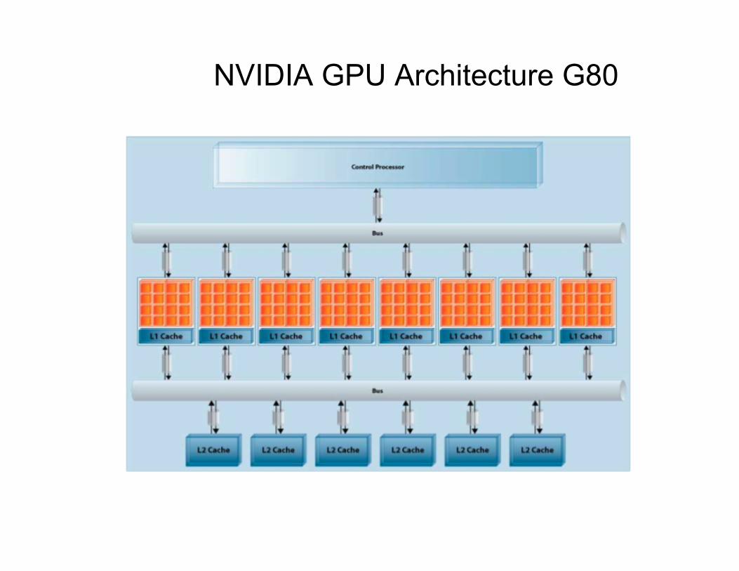
NVIDIA GPU Architecture G80
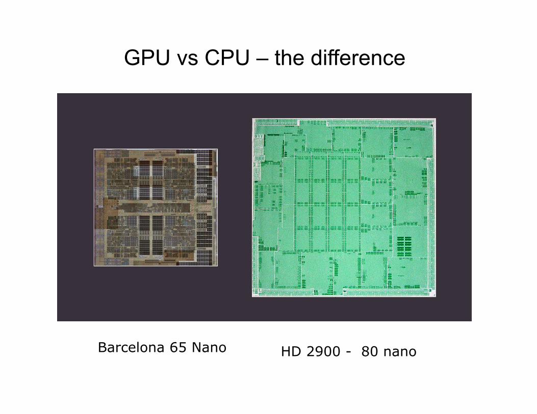
HD 2900 - 80 nano Barcelona 65 Nano
GPU vs CPU – the difference
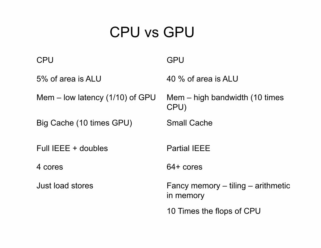
CPU vs GPU
CPU GPU
5% of area is ALU 40 % of area is ALU
Mem – low latency (1/10) of GPU Mem – high bandwidth (10 times CPU)
Big Cache (10 times GPU) Small Cache
Full IEEE + doubles Partial IEEE
4 cores 64+ cores
Just load stores Fancy memory – tiling – arithmetic in memory
10 Times the flops of CPU
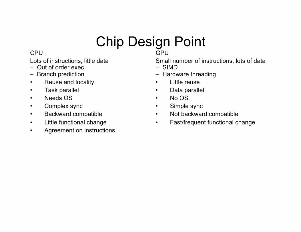
Chip Design Point CPU Lots of instructions, little data – Out of order exec – Branch prediction • Reuse and locality • Task parallel • Needs OS • Complex sync • Backward compatible • Little functional change • Agreement on instructions
GPU Small number of instructions, lots of data – SIMD – Hardware threading • Little reuse • Data parallel • No OS • Simple sync • Not backward compatible • Fast/frequent functional change
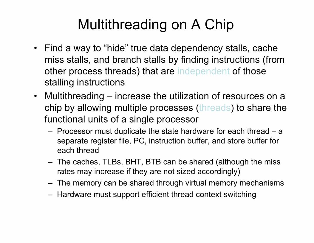
Multithreading on A Chip • Find a way to “hide” true data dependency stalls, cache
miss stalls, and branch stalls by finding instructions (from other process threads) that are independent of those stalling instructions
• Multithreading – increase the utilization of resources on a chip by allowing multiple processes (threads) to share the functional units of a single processor – Processor must duplicate the state hardware for each thread – a
separate register file, PC, instruction buffer, and store buffer for each thread
– The caches, TLBs, BHT, BTB can be shared (although the miss rates may increase if they are not sized accordingly)
– The memory can be shared through virtual memory mechanisms – Hardware must support efficient thread context switching
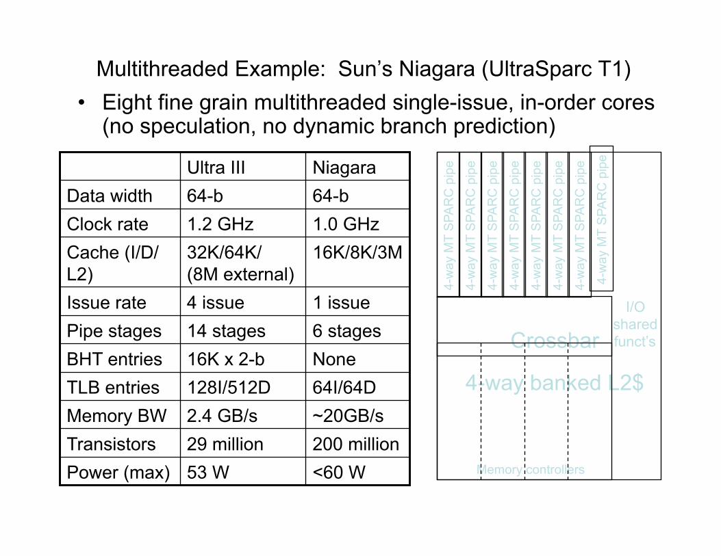
Multithreaded Example: Sun’s Niagara (UltraSparc T1) • Eight fine grain multithreaded single-issue, in-order cores
(no speculation, no dynamic branch prediction)
<60 W 53 W Power (max) 200 million 29 million Transistors ~20GB/s 2.4 GB/s Memory BW 64I/64D 128I/512D TLB entries None 16K x 2-b BHT entries 6 stages 14 stages Pipe stages 1 issue 4 issue Issue rate
16K/8K/3M 32K/64K/ (8M external)
Cache (I/D/L2)
1.0 GHz 1.2 GHz Clock rate 64-b 64-b Data width Niagara Ultra III
4-w
ay M
T S
PAR
C p
ipe
4-w
ay M
T S
PAR
C p
ipe
4-w
ay M
T S
PAR
C p
ipe
4-w
ay M
T S
PAR
C p
ipe
4-w
ay M
T S
PAR
C p
ipe
4-w
ay M
T S
PAR
C p
ipe
4-w
ay M
T S
PAR
C p
ipe
4-w
ay M
T S
PAR
C p
ipe
Crossbar
4-way banked L2$
Memory controllers
I/O shared funct’s

Niagara Integer Pipeline • Cores are simple (single-issue, 6 stage, no branch
prediction), small, and power-efficient Fetch Thrd Sel Decode Execute Memory WB
I$
ITLB
Inst bufx4
PC logicx4
Decode
RegFilex4
Thread Select Logic
ALU Mul Shft Div
D$
DTLB Stbufx4
Thrd Sel Mux
Thrd Sel Mux
Crossbar Interface
Instr type Cache misses Traps & interrupts Resource conflicts
From MPR, Vol. 18, #9, Sept. 2004
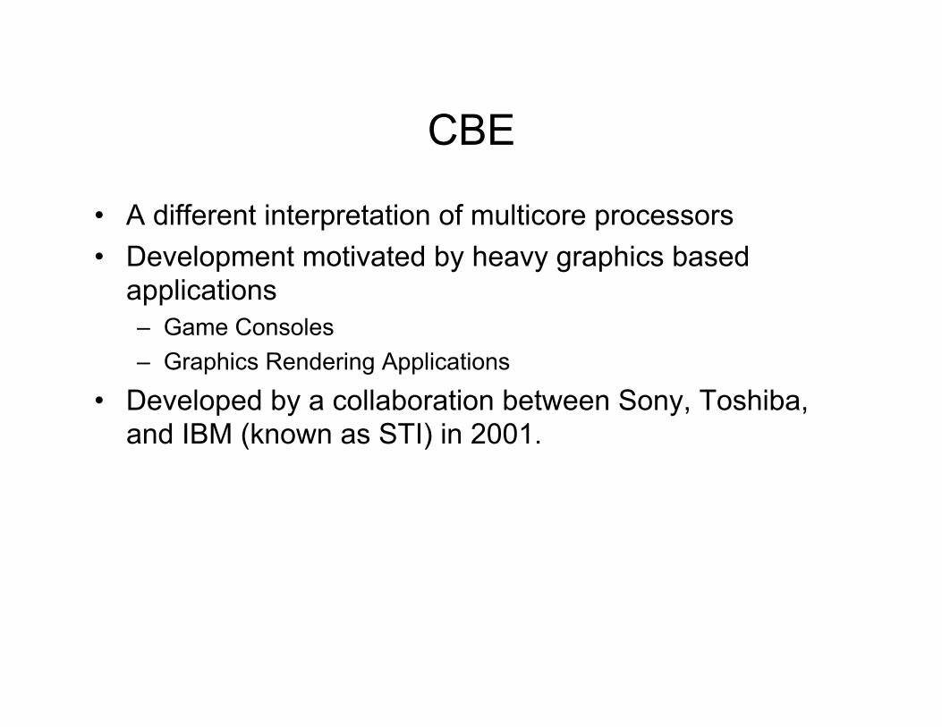
CBE
• A different interpretation of multicore processors • Development motivated by heavy graphics based
applications – Game Consoles – Graphics Rendering Applications
• Developed by a collaboration between Sony, Toshiba, and IBM (known as STI) in 2001.
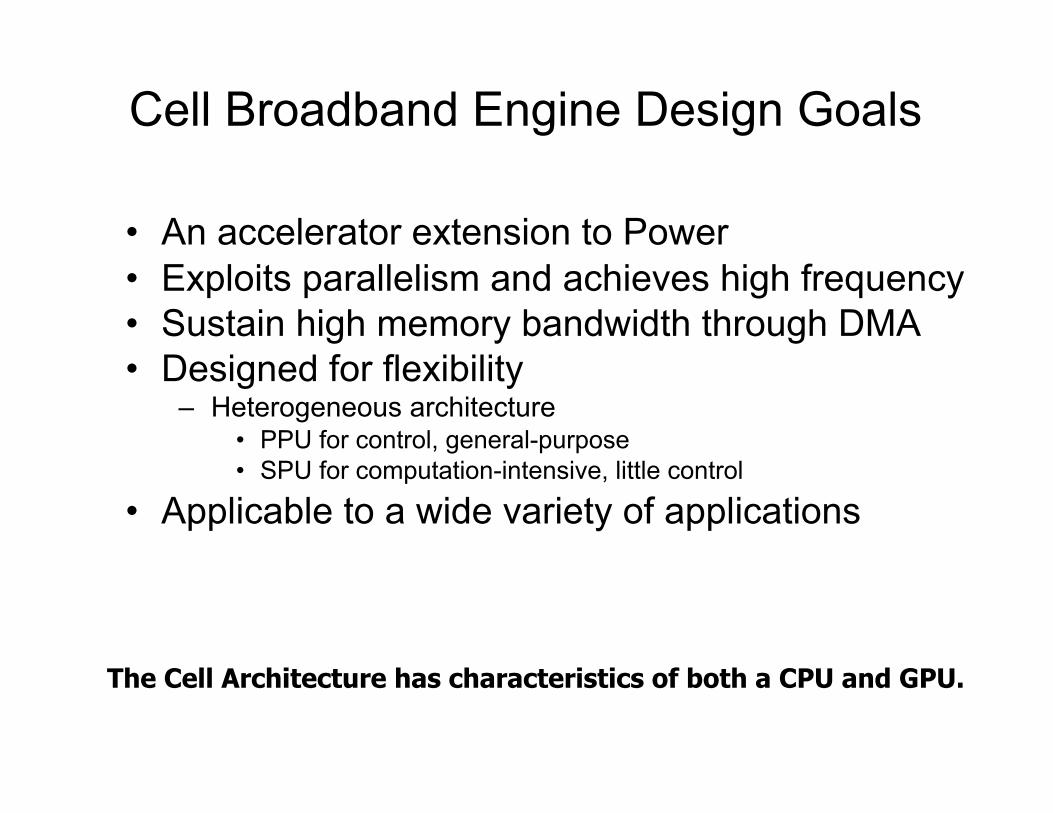
Cell Broadband Engine Design Goals
• An accelerator extension to Power • Exploits parallelism and achieves high frequency • Sustain high memory bandwidth through DMA • Designed for flexibility
– Heterogeneous architecture • PPU for control, general-purpose • SPU for computation-intensive, little control
• Applicable to a wide variety of applications
The Cell Architecture has characteristics of both a CPU and GPU.
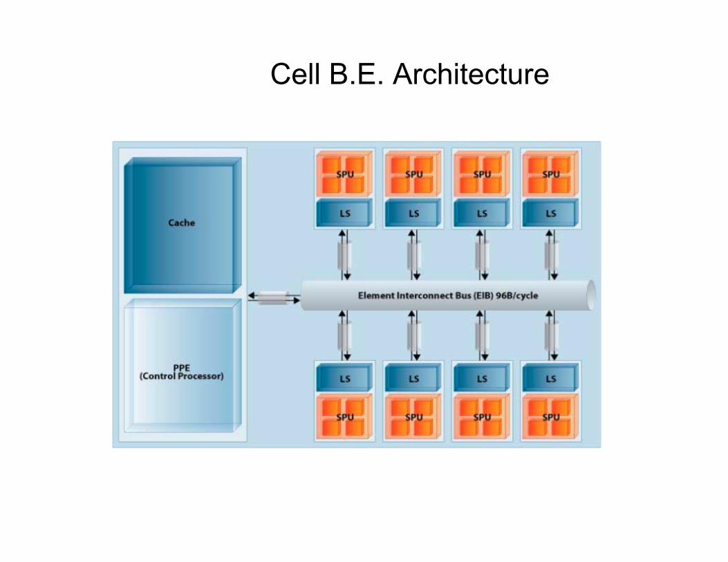
Cell B.E. Architecture

Architecture Components
• PPE (Power Processing Elements) – Main processing unit. – Controls SPE units
• EIB (Element Interconnect Bus) – Communication Bus
• SPEs (Synergistic Processor Element ) – Non-control Processor Elements – 8 on chip
• BEI (Broadband Engine Interface) – Engine Interface
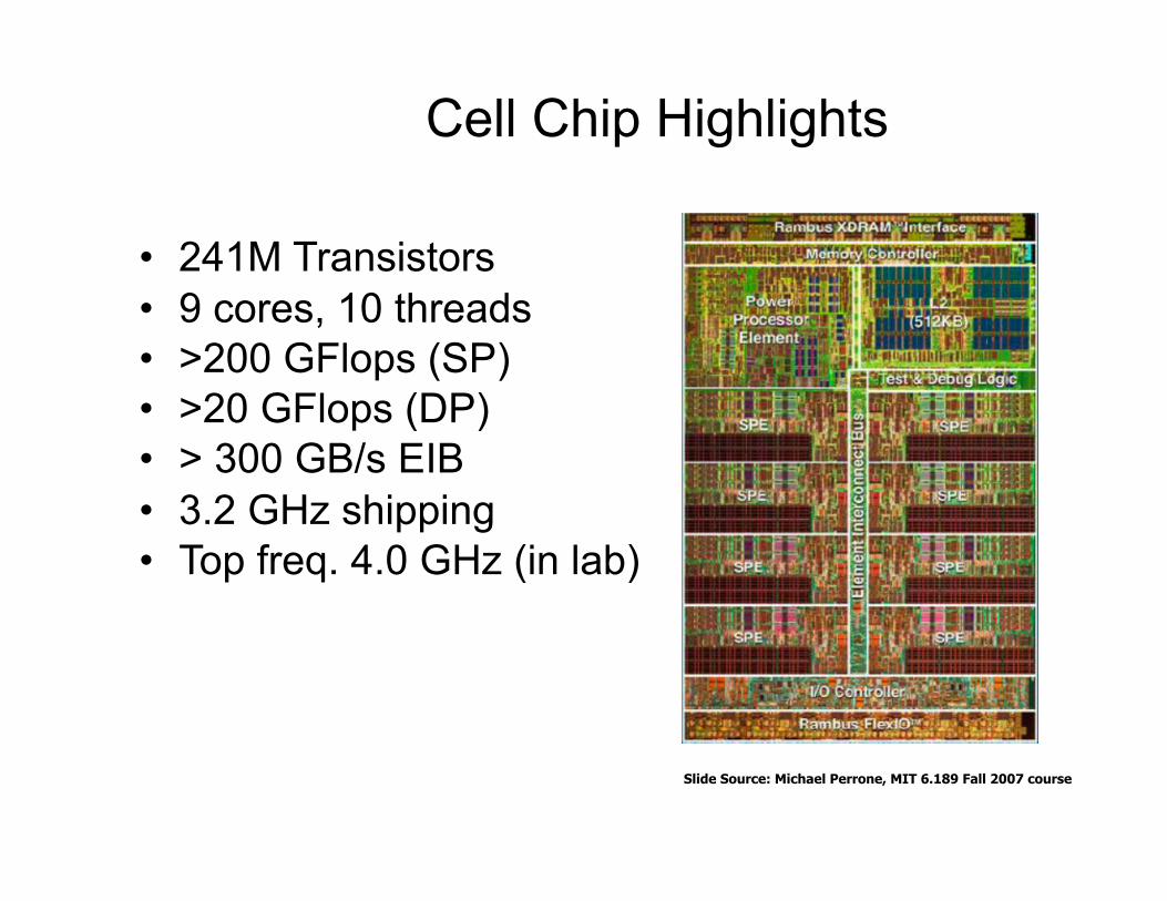
Cell Chip Highlights
Slide Source: Michael Perrone, MIT 6.189 Fall 2007 course
• 241M Transistors • 9 cores, 10 threads • >200 GFlops (SP) • >20 GFlops (DP) • > 300 GB/s EIB • 3.2 GHz shipping • Top freq. 4.0 GHz (in lab)
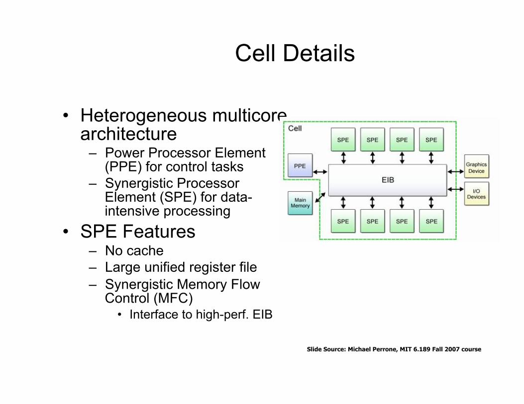
Cell Details
Slide Source: Michael Perrone, MIT 6.189 Fall 2007 course
• Heterogeneous multicore architecture
– Power Processor Element (PPE) for control tasks
– Synergistic Processor Element (SPE) for data-intensive processing
• SPE Features – No cache – Large unified register file – Synergistic Memory Flow
Control (MFC) • Interface to high-perf. EIB
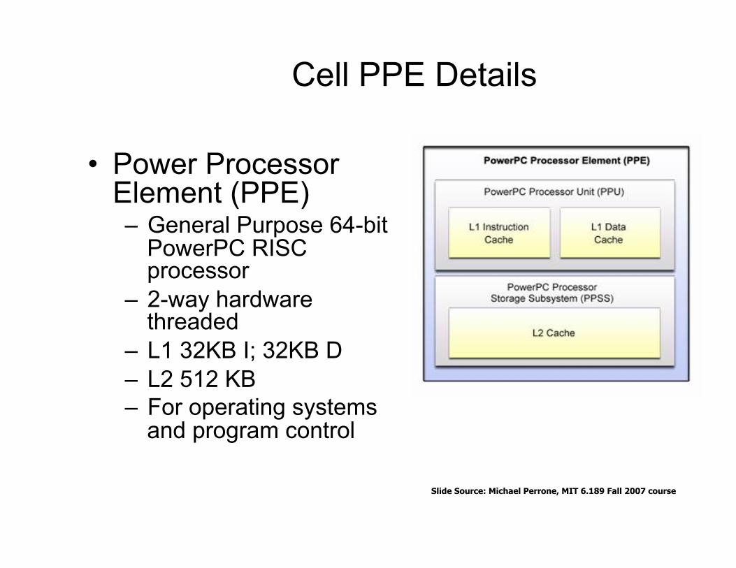
Cell PPE Details
Slide Source: Michael Perrone, MIT 6.189 Fall 2007 course
• Power Processor Element (PPE) – General Purpose 64-bit
PowerPC RISC processor
– 2-way hardware threaded
– L1 32KB I; 32KB D – L2 512 KB – For operating systems
and program control
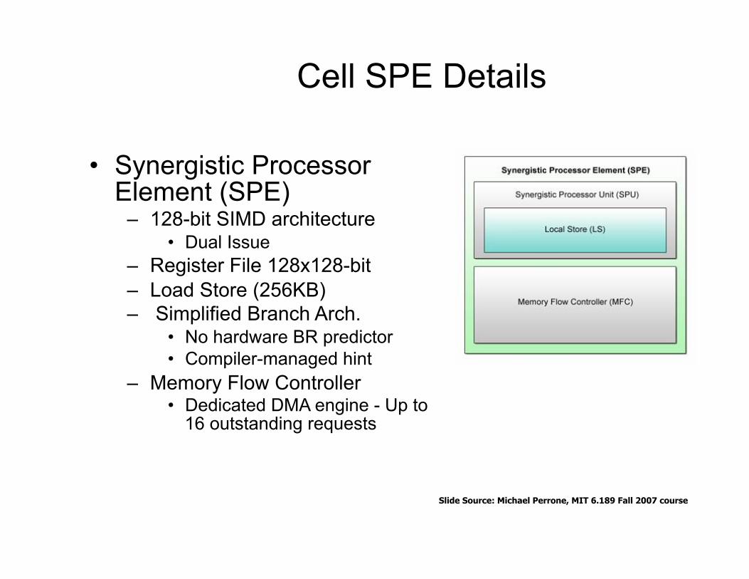
Cell SPE Details
Slide Source: Michael Perrone, MIT 6.189 Fall 2007 course
• Synergistic Processor Element (SPE)
– 128-bit SIMD architecture • Dual Issue
– Register File 128x128-bit – Load Store (256KB) – Simplified Branch Arch.
• No hardware BR predictor • Compiler-managed hint
– Memory Flow Controller • Dedicated DMA engine - Up to
16 outstanding requests

Commercial Multicores

Many-core array • CMP with 10s-100s low
power cores • Scalar cores • Capable of TFLOPS+ • Full System-on-Chip • Servers, workstations,
embedded…
Dual core • Symmetric multithreading
Multi-core array • CMP with ~10 cores
Evolution
Large, Scalar cores for high single-thread performance
Scalar plus many core for highly threaded workloads
Evolutionary Architecture
CMP = “chip multi-processor” Presentation Paul Petersen, Sr. Principal Engineer, Intel 43
Intel Teraflops (80-core chip) Video
http://www.youtube.com/watch?v=TAKG0UvtzpE
Recommended