
8/10/2019 PIC16F684 Datasheet
http://slidepdf.com/reader/full/pic16f684-datasheet 1/192
© 2007 Microchip Technology Inc. DS41202F
PIC16F684Data Sheet
14-Pin, Flash-Based 8-Bit
CMOS Microcontrollers
with nanoWatt Technology
8/10/2019 PIC16F684 Datasheet
http://slidepdf.com/reader/full/pic16f684-datasheet 2/192
8/10/2019 PIC16F684 Datasheet
http://slidepdf.com/reader/full/pic16f684-datasheet 3/192
© 2007 Microchip Technology Inc. DS41202F-page 1
PIC16F684
High-Performance RISC CPU:
• Only 35 instructions to learn:
- All single-cycle instructions except branches
• Operating speed:
- DC – 20 MHz oscillator/clock input
- DC – 200 ns instruction cycle
• Interrupt capability
• 8-level deep hardware stack
• Direct, Indirect and Relative Addressing modes
Special Microcontroller Features:
• Precision Internal Oscillator:
- Factory calibrated to ±1%, typical
- Software selectable frequency range of
8 MHz to 125 kHz
- Software tunable
- Two-Speed Start-up mode
- Crystal fail detect for critical applications
- Clock mode switching during operation for
power savings
• Software Selectable 31 kHz Internal Oscillator
• Power-Saving Sleep mode
• Wide operating voltage range (2.0V-5.5V)
• Industrial and Extended Temperature range• Power-on Reset (POR)
• Power-up Timer (PWRT) and Oscillator Start-up
Timer (OST)
• Brown-out Reset (BOR) with software control
option
• Enhanced low-current Watchdog Timer (WDT)
with on-chip oscillator (software selectable
nominal 268 seconds with full prescaler) with
software enable
• Multiplexed Master Clear with pull-up/input pin
• Programmable code protection
• High Endurance Flash/EEPROM cell:
- 100,000 write Flash endurance- 1,000,000 write EEPROM endurance
- Flash/Data EEPROM retention: > 40 years
Low-Power Features:
• Standby Current:
- 50 nA @ 2.0V, typical
• Operating Current:
- 11 µA @ 32 kHz, 2.0V, typical
- 220 µA @ 4 MHz, 2.0V, typical
• Watchdog Timer Current:
- 1 µA @ 2.0V, typical
Peripheral Features:
• 12 I/O pins with individual direction control:- High current source/sink for direct LED drive
- Interrupt-on-change pin
- Individually programmable weak pull-ups
- Ultra Low-Power Wake-Up (ULPWU)
• Analog Comparator module with:
- Two analog comparators
- Programmable on-chip voltage reference
(CVREF) module (% of VDD)
- Comparator inputs and outputs externally
accessible
• A/D Converter:
- 10-bit resolution and 8 channels
• Timer0: 8-bit timer/counter with 8-bitprogrammable prescaler
• Enhanced Timer1:
- 16-bit timer/counter with prescaler
- External Timer1 Gate (count enable)
- Option to use OSC1 and OSC2 in LP mode
as Timer1 oscillator if INTOSC mode
selected
• Timer2: 8-bit timer/counter with 8-bit period
register, prescaler and postscaler
• Enhanced Capture, Compare, PWM module:
- 16-bit Capture, max resolution 12.5 ns
- Compare, max resolution 200 ns
- 10-bit PWM with 1, 2 or 4 output channels,programmable “dead time”, max frequency
20 kHz
• In-Circuit Serial ProgrammingTM (ICSPTM) via two
pins
Device
Program
MemoryData Memory
I/O10-bit A/D
(ch)Comparators
Timers
8/16-bitFlash
(words)
SRAM
(bytes)
EEPROM
(bytes)
PIC16F684 2048 128 256 12 8 2 2/1
14-Pin Flash-Based, 8-Bit CMOS Microcontrollers with nanoWatt Technology
8/10/2019 PIC16F684 Datasheet
http://slidepdf.com/reader/full/pic16f684-datasheet 4/192
PIC16F684
DS41202F-page 2 © 2007 Microchip Technology Inc.
14-Pin Diagram (PDIP, SOIC, TSSOP)
TABLE 1: DUAL IN-LINE PIN SUMMARY
I/O Pin Analog Comparators Timer CCP Interrupts Pull-ups Basic
RA0 13 AN0 C1IN+ — — IOC Y ICSPDAT/ULPWU
RA1 12 AN1/VREF C1IN- — — IOC Y ICSPCLK
RA2 11 AN2 C1OUT T0CKI — INT/IOC Y —
RA3(1)4 — — — — IOC Y(2) MCLR/VPP
RA4 3 AN3 — T1G — IOC Y OSC2/CLKOUTRA5 2 — — T1CKI — IOC Y OSC1/CLKIN
RC0 10 AN4 C2IN+ — — — — —
RC1 9 AN5 C2IN- — — — — —
RC2 8 AN6 — — P1D — — —
RC3 7 AN7 — — P1C — — —
RC4 6 — C2OUT — P1B — — —
RC5 5 — — — CCP1/P1A — — —
— 1 — — — — — — VDD
— 14 — — — — — — VSS
Note 1: Input only.
2: Only when pin is configured for external MCLR.
VDD
RA5/T1CKI/OSC1/CLKIN
RA4/AN3/T1G/OSC2/CLKOUT
RA3/MCLR/VPP
RC5/CCP1/P1ARC4/C2OUT/P1B
RC3/AN7/P1C
VSS
RA0/AN0/C1IN+/ICSPDAT/ULPWU
RA1/AN1/C1IN-/VREF /ICSPCLK
RA2/AN2/T0CKI/INT/C1OUT
RC0/AN4/C2IN+RC1/AN5/C2IN-
RC2/AN6/P1D
P I C
1 6 F 6 8 4
1
2
3
4
56
7
14
13
12
9
11
10
8
8/10/2019 PIC16F684 Datasheet
http://slidepdf.com/reader/full/pic16f684-datasheet 5/192
© 2007 Microchip Technology Inc. DS41202F-page 3
PIC16F684
16-Pin Diagram (QFN)
TABLE 2: QFN PIN SUMMARY
I/O Pin Analog Comparators Timers CCP Interrupts Pull-ups Basic
RA0 12 AN0 C1IN+ — — IOC Y ICSPDAT/ULPWU
RA1 11 AN1/VREF C1IN- — — IOC Y ICSPCLK
RA2 10 AN2 C1OUT T0CKI — INT/IOC Y —
RA3(1)3 — — — — IOC Y(2) MCLR/VPP
RA4 2 AN3 — T1G — IOC Y OSC2/CLKOUT
RA5 1 — — T1CKI — IOC Y OSC1/CLKIN
RC0 9 AN4 C2IN+ — — — — —
RC1 8 AN5 C2IN- — — — — —
RC2 7 AN6 — — P1D — — —
RC3 6 AN7 — — P1C — — —
RC4 5 — C2OUT — P1B — — —
RC5 4 — — — CCP1/P1A — — —
— 16 — — — — — — VDD
— 13 — — — — — — VSS
Note 1: Input only.
2: Only when pin is configured for external MCLR.
1
2
3
4 9
10
11
12
5 6 7 8
1 6 1 5 1 4 1 3
PIC16F684
RA5/T1CKI/OSC1/CLKIN
RA4/AN3/T1G/OSC2/CLKOUT
RA3/MCLR/VPP
RC5/CCP1/P1A
V D D
N C
N C
V S S
RA0/AN0/C1IN+/ICSPDAT/ULPWU
RA1/AN1/C1IN-/VREF /ICSPCLK
RA2/AN2/T0CKI/INT/C1OUT
RC0/AN4/C2IN+
R C
4 / C 2 O U T / P 1 B
R C 3 / A N 7 / P 1 C
R C 2 / A N 6 / P 1 D
R
C 1 / A N 5 / C 2 I N -
8/10/2019 PIC16F684 Datasheet
http://slidepdf.com/reader/full/pic16f684-datasheet 6/192
PIC16F684
DS41202F-page 4 © 2007 Microchip Technology Inc.
Table of Contents
1.0 Device Overview .......................................................................................................................................................................... 5
2.0 Memory Organization ................................................................................................................................................................... 7
3.0 Oscillator Module (With Fail-Safe Clock Monitor)....................................................................................................................... 19
4.0 I/O Ports ..................................................................................................................................................................................... 31
5.0 Timer0 Module ........................................................................................................................................................................... 43
6.0 Timer1 Module with Gate Control............................................................................................................................................... 47
7.0 Timer2 Module ........................................................................................................................................................................... 538.0 Comparator Module.................................................................................................................................................................... 55
9.0 Analog-to-Digital Converter (ADC) Module ................................................................................................................................ 65
10.0 Data EEPROM Memory ............................................................................................................................................................. 75
11.0 Enhanced Capture/Compare/PWM (With Auto-Shutdown and Dead Band) Module................................................................. 79
12.0 Special Features of the CPU...................................................................................................................................................... 97
13.0 Instruction Set Summary .......................................................................................................................................................... 115
14.0 Development Support............................................................................................................................................................... 125
15.0 Electrical Specifications............................................................................................................................................................ 129
16.0 DC and AC Characteristics Graphs and Tables....................................................................................................................... 151
17.0 Packaging Information.............................................................................................................................................................. 173
Appendix A: Data Sheet Revision History..... ................. ................ ............... ............... ................. ................ ............... ............... ....... 179
Appendix B: Migrating from other PIC® Devices ............... ................. ................ ............... ............... ................. ................ ............... . 179
Index .................................................................................................................................................................................................. 181
The Microchip Web Site ............... ................. ................ ............... ................. ............... .............. ................. ............... ............... ......... 187
Customer Change Notification Service ............... ............... ................. ................ ............... ............... ................. ................ ............... . 187
Customer Support. ............... ................ ............... ............... ................. ................ ............... ............... ................. ................ ............... . 187
Reader Response ................ ................ ............... ............... ................. ................ ............... ............... ................. ................ ............... . 188
Product Identification System................. ............... ................. ............... ................ ................. ............... ............... ................ .............. 189
TO OUR VALUED CUSTOMERS
It is our intention to provide our valued customers with the best documentation possible to ensure successful use of your Microchip
products. To this end, we will continue to improve our publications to better suit your needs. Our publications will be refined and
enhanced as new volumes and updates are introduced.
If you have any questions or comments regarding this publication, please contact the Marketing Communications Department via
E-mail at [email protected] or fax the Reader Response Form in the back of this data sheet to (480) 792-4150. We
welcome your feedback.
Most Current Data SheetTo obtain the most up-to-date version of this data sheet, please register at our Worldwide Web site at:
http://www.microchip.com
You can determine the version of a data sheet by examining its literature number found on the bottom outside corner of any page.The last character of the literature number is the version number, (e.g., DS30000A is version A of document DS30000).
Errata
An errata sheet, describing minor operational differences from the data sheet and recommended workarounds, may exist for currentdevices. As device/documentation issues become known to us, we will publish an errata sheet. The errata will specify the revision ofsilicon and revision of document to which it applies.
To determine if an errata sheet exists for a particular device, please check with one of the following:
• Microchip’s Worldwide Web site; http://www.microchip.com
• Your local Microchip sales office (see last page)
When contacting a sales office, please specify which device, revision of silicon and data sheet (include literature number) you are
using.
Customer Notification System
Register on our web site at www.microchip.com to receive the most current information on all of our products.
8/10/2019 PIC16F684 Datasheet
http://slidepdf.com/reader/full/pic16f684-datasheet 7/192
© 2007 Microchip Technology Inc. DS41202F-page 5
PIC16F684
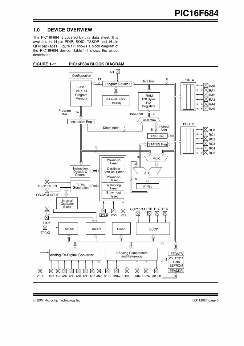
1.0 DEVICE OVERVIEW
The PIC16F684 is covered by this data sheet. It is
available in 14-pin PDIP, SOIC, TSSOP and 16-pin
QFN packages. Figure 1-1 shows a block diagram of
the PIC16F684 device. Table 1-1 shows the pinout
description.
FIGURE 1-1: PIC16F684 BLOCK DIAGRAM
Flash
ProgramMemory
13Data Bus
8
14ProgramBus
Instruction Reg
Program Counter
RAM
FileRegisters
Direct Addr 7
RAM Addr 9
Addr MUX
IndirectAddr
FSR Reg
STATUS Reg
MUX
ALU
W Reg
InstructionDecode &
Control
TimingGenerationOSC1/CLKIN
OSC2/CLKOUT
PORTA
8
8
8
3
8-Level Stack 128 Bytes
2k X 14
(13-Bit)
Power-upTimer
OscillatorStart-up Timer
Power-on
ResetWatchdog
Timer
MCLR VSS
Brown-outReset
Timer0 Timer1
DataEEPROM
256 Bytes
EEDATA
EEADDR
RA0
RA1
RA2
RA3
RA4
RA5
2 Analog ComparatorsAnalog-To-Digital Converter
AN0 AN1 AN2 AN3 C1IN- C1IN+ C1OUT
T0CKI
INT
T1CKI
Configuration
InternalOscillator
VREF
and Reference
T1G
PORTC
RC0
RC1
RC2
RC3
RC4
RC5
AN4 AN5 AN6 AN7
VDD
8
Timer2
C2IN- C2IN+ C2OUT
ECCP
BlockCCP1/P1A P1B P1C P1D

8/10/2019 PIC16F684 Datasheet
http://slidepdf.com/reader/full/pic16f684-datasheet 8/192
PIC16F684
DS41202F-page 6 © 2007 Microchip Technology Inc.
TABLE 1-1: PIC16F684 PINOUT DESCRIPTION
Name FunctionInput
Type
Output
TypeDescription
RA0/AN0/C1IN+/ICSPDAT/ULPWU RA0 TTL CMOS PORTA I/O with prog. pull-up and interrupt-on-change
AN0 AN — A/D Channel 0 input
C1IN+ AN — Comparator 1 non-inverting input
ICSPDAT TTL CMOS Serial Programming Data I/OULPWU AN — Ultra Low-Power Wake-Up input
RA1/AN1/C1IN-/VREF /ICSPCLK RA1 TTL CMOS PORTA I/O with prog. pull-up and interrupt-on-change
AN1 AN — A/D Channel 1 input
C1IN- AN — Comparator 1 inverting input
VREF AN — External Voltage Reference for A/D
ICSPCLK ST — Serial Programming Clock
RA2/AN2/T0CKI/INT/C1OUT RA2 ST CMOS PORTA I/O with prog. pull-up and interrupt-on-change
AN2 AN — A/D Channel 2 input
T0CKI ST — Timer0 clock input
INT ST — External Interrupt
C1OUT — CMOS Comparator 1 output
RA3/MCLR/VPP RA3 TTL — PORTA input with interrupt-on-changeMCLR ST — Master Clear w/internal pull-up
VPP HV — Programming voltage
RA4/AN3/T1G/OSC2/CLKOUT RA4 TTL CMOS PORTA I/O with prog. pull-up and interrupt-on-change
AN3 AN — A/D Channel 3 input
T1G ST — Timer1 gate (count enable)
OSC2 — XTAL Crystal/Resonator
CLKOUT — CMOS FOSC /4 output
RA5/T1CKI/OSC1/CLKIN RA5 TTL CMOS PORTA I/O with prog. pull-up and interrupt-on-change
T1CKI ST — Timer1 clock
OSC1 XTAL — Crystal/Resonator
CLKIN ST — External clock input/RC oscillator connection
RC0/AN4/C2IN+ RC0 TTL CMOS PORTC I/OAN4 AN — A/D Channel 4 input
C2IN+ AN — Comparator 2 non-inverting input
RC1/AN5/C2IN- RC1 TTL CMOS PORTC I/O
AN5 AN — A/D Channel 5 input
C2IN- AN — Comparator 2 inverting input
RC2/AN6/P1D RC2 TTL CMOS PORTC I/O
AN6 AN — A/D Channel 6 input
P1D — CMOS PWM output
RC3/AN7/P1C RC3 TTL CMOS PORTC I/O
AN7 AN — A/D Channel 7 input
P1C — CMOS PWM output
RC4/C2OUT/P1B RC4 TTL CMOS PORTC I/OC2OUT — CMOS Comparator 2 output
P1B — CMOS PWM output
RC5/CCP1/P1A RC5 TTL CMOS PORTC I/O
CCP1 ST CMOS Capture input/Compare output
P1A — CMOS PWM output
VDD VDD Power — Positive supply
VSS VSS Power — Ground reference
Legend: AN = Analog input or output CMOS= CMOS compatible input or output HV = High Voltage
ST = Schmitt Trigger input with CMOS levels TTL = TTL compatible input XTAL = Crystal
8/10/2019 PIC16F684 Datasheet
http://slidepdf.com/reader/full/pic16f684-datasheet 9/192
© 2007 Microchip Technology Inc. DS41202F-page 7
PIC16F684
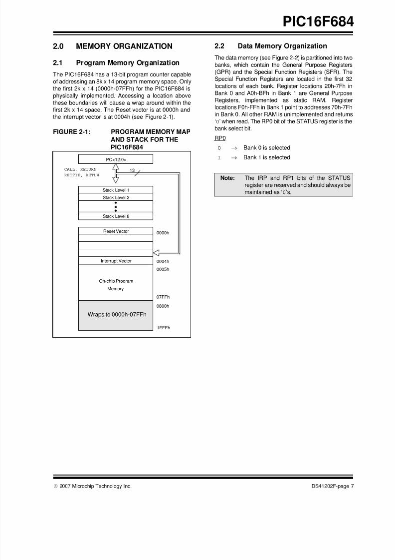
2.0 MEMORY ORGANIZATION
2.1 Program Memory Organization
The PIC16F684 has a 13-bit program counter capable
of addressing an 8k x 14 program memory space. Only
the first 2k x 14 (0000h-07FFh) for the PIC16F684 is
physically implemented. Accessing a location abovethese boundaries will cause a wrap around within the
first 2k x 14 space. The Reset vector is at 0000h and
the interrupt vector is at 0004h (see Figure 2-1).
FIGURE 2-1: PROGRAM MEMORY MAP
AND STACK FOR THEPIC16F684
2.2 Data Memory Organization
The data memory (see Figure 2-2) is partitioned into two
banks, which contain the General Purpose Registers
(GPR) and the Special Function Registers (SFR). The
Special Function Registers are located in the first 32
locations of each bank. Register locations 20h-7Fh in
Bank 0 and A0h-BFh in Bank 1 are General Purpose
Registers, implemented as static RAM. Registerlocations F0h-FFh in Bank 1 point to addresses 70h-7Fh
in Bank 0. All other RAM is unimplemented and returns
‘0’ when read. The RP0 bit of the STATUS register is the
bank select bit.
RP0
0 → Bank 0 is selected
1 → Bank 1 is selectedPC<12:0>
13
0000h
0004h
0005h
07FFh
0800h
1FFFh
Stack Level 1
Stack Level 8
Reset Vector
Interrupt Vector
On-chip Program
Memory
CALL, RETURN
RETFIE, RETLW
Stack Level 2
Wraps to 0000h-07FFh
Note: The IRP and RP1 bits of the STATUS
register are reserved and should always be
maintained as ‘0’s.

8/10/2019 PIC16F684 Datasheet
http://slidepdf.com/reader/full/pic16f684-datasheet 10/192
PIC16F684
DS41202F-page 8 © 2007 Microchip Technology Inc.
2.2.1 GENERAL PURPOSE REGISTER
FILE
The register file is organized as 128 x 8 in the
PIC16F684. Each register is accessed, either directly
or indirectly, through the File Select Register (FSR)
(see Section 2.4 “Indirect Addressing, INDF and
FSR Registers”).
2.2.2 SPECIAL FUNCTION REGISTERS
The Special Function Registers are registers used by
the CPU and peripheral functions for controlling the
desired operation of the device (see Table 2-1). These
registers are static RAM.
The special registers can be classified into two sets:
core and peripheral. The Special Function Registers
associated with the “core” are described in this section.
Those related to the operation of the peripheral features
are described in the section of that peripheral feature.
FIGURE 2-2: DATA MEMORY MAP OF
THE PIC16F684
Indirect Addr.(1)
TMR0
PCLSTATUS
FSR
PORTA
PCLATH
INTCON
PIR1
TMR1L
TMR1H
T1CON
00h
01h
02h03h
04h
05h
06h
07h
08h
09h
0Ah
0Bh
0Ch
0Dh
0Eh
0Fh
10h
11h
12h
13h
14h
15h
16h
17h
18h
19h
1Ah
1Bh
1Ch
1Dh
1Eh
1Fh
20h
7Fh
Bank 0
Unimplemented data memory locations, read as ‘0’.
Note 1: Not a physical register.
CMCON0 VRCON
General
Purpose
Registers
96 Bytes
EEDAT
EEADR
EECON2(1)
File
Address
File
Address
WPUA
IOCA
Indirect Addr.(1)
OPTION_REG
PCLSTATUS
FSR
TRISA
PCLATH
INTCON
PIE1
PCON
80h
81h
82h83h
84h
85h
86h
87h
88h
89h
8Ah
8Bh
8Ch
8Dh
8Eh
8Fh
90h
91h
92h
93h
94h
95h
96h
97h
98h
99h
9Ah
9Bh
9Ch
9Dh
9Eh
9Fh
A0h
FFh
Bank 1
ADRESH
ADCON0
EECON1
ADRESL
ADCON1
ANSEL
TRISCPORTC
BFh
General
Purpose
Registers
32 Bytes
Accesses 70h-7FhF0h
TMR2
T2CON
CCPR1L
CCPR1H
CCP1CON
PWM1CON
ECCPAS
WDTCON
CMCON1
OSCCON
OSCTUNE
PR2
70
6Fh
8/10/2019 PIC16F684 Datasheet
http://slidepdf.com/reader/full/pic16f684-datasheet 11/192
© 2007 Microchip Technology Inc. DS41202F-page 9
PIC16F684
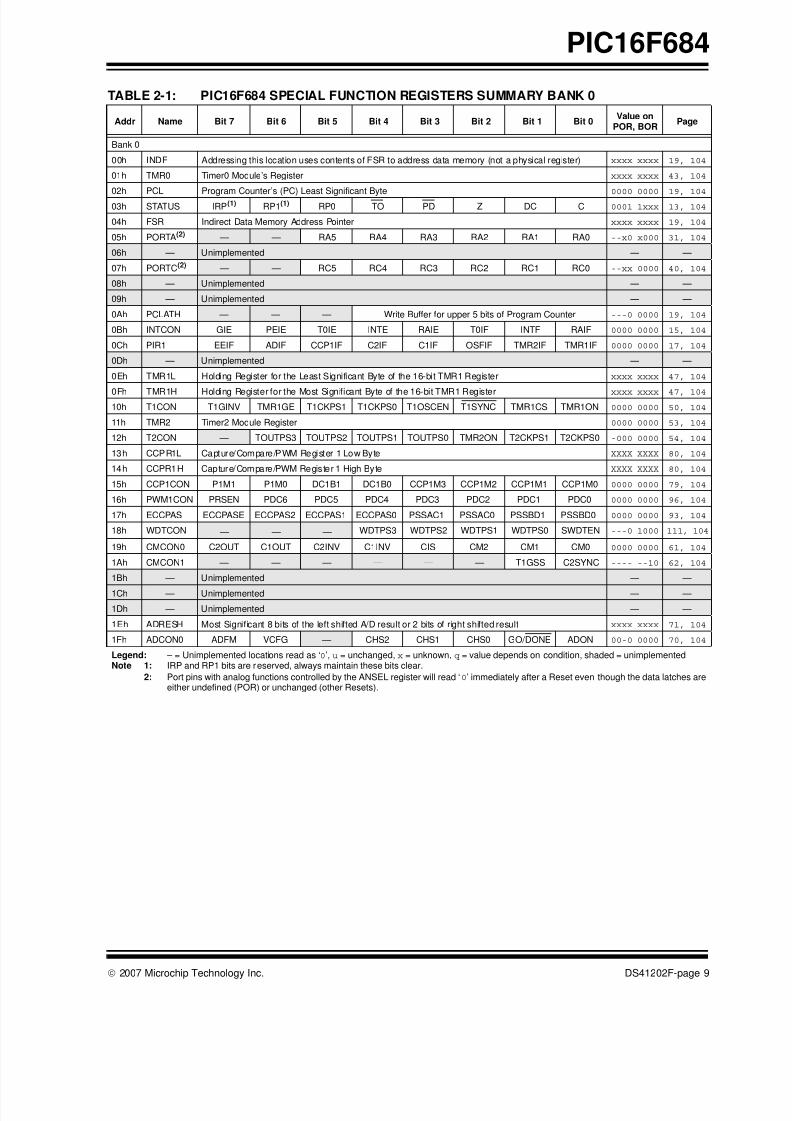
TABLE 2-1: PIC16F684 SPECIAL FUNCTION REGISTERS SUMMARY BANK 0
Addr Name Bit 7 Bit 6 Bit 5 Bit 4 Bit 3 Bit 2 Bit 1 Bit 0Value on
POR, BORPage
Bank 0
00h INDF Addressing this location uses contents of FSR to address data memory (not a physical register) xxxx xxxx 19, 104
01h TMR0 Timer0 Module’s Register xxxx xxxx 43, 104
02h PCL Program Counter’s (PC) Least Significant Byte 0000 0000 19, 104
03h STATUS IRP(1) RP1(1) RP0 TO PD Z DC C 0001 1xxx 13, 104
04h FSR Indirect Data Memory Address Pointer xxxx xxxx 19, 104
05h PORTA(2) — — RA5 RA4 RA3 RA2 RA1 RA0 --x0 x000 31, 104
06h — Unimplemented — —
07h PORTC(2) — — RC5 RC4 RC3 RC2 RC1 RC0 --xx 0000 40, 104
08h — Unimplemented — —
09h — Unimplemented — —
0Ah PCLATH — — — Write Buffer for upper 5 bits of Program Counter ---0 0000 19, 104
0Bh INTCON GIE PEIE T0IE INTE RAIE T0IF INTF RAIF 0000 0000 15, 104
0Ch PIR1 EEIF ADIF CCP1IF C2IF C1IF OSFIF TMR2IF TMR1IF 0000 0000 17, 104
0Dh — Unimplemented — —
0Eh TMR1L Holding Register for the Least Significant Byte of the 16-bit TMR1 Register xxxx xxxx 47, 104
0Fh TMR1H Holding Register for the Most Significant Byte of the 16-bit TMR1 Register xxxx xxxx 47, 104
10h T1CON T1GINV TMR1GE T1CKPS1 T1CKPS0 T1OSCEN T1SYNC TMR1CS TMR1ON 0000 0000 50, 104
11h TMR2 Timer2 Module Register 0000 0000 53, 104
12h T2CON — TOUTPS3 TOUTPS2 TOUTPS1 TOUTPS0 TMR2ON T2CKPS1 T2CKPS0 -000 0000 54, 104
13h CCPR1L Capture/Compare/PWM Register 1 Low Byte XXXX XXXX 80, 104
14h CCPR1H Capture/Compare/PWM Register 1 High Byte XXXX XXXX 80, 104
15h CCP1CON P1M1 P1M0 DC1B1 DC1B0 CCP1M3 CCP1M2 CCP1M1 CCP1M0 0000 0000 79, 104
16h PWM1CON PRSEN PDC6 PDC5 PDC4 PDC3 PDC2 PDC1 PDC0 0000 0000 96, 104
17h ECCPAS ECCPASE ECCPAS2 ECCPAS1 ECCPAS0 PSSAC1 PSSAC0 PSSBD1 PSSBD0 0000 0000 93, 104
18h WDTCON — — — WDTPS3 WDTPS2 WDTPS1 WDTPS0 SWDTEN ---0 1000 111, 104
19h CMCON0 C2OUT C1OUT C2INV C1INV CIS CM2 CM1 CM0 0000 0000 61, 104
1Ah CMCON1 — — — — — — T1GSS C2SYNC ---- --10 62, 104
1Bh — Unimplemented — —
1Ch — Unimplemented — —
1Dh — Unimplemented — —
1Eh ADRESH Most Significant 8 bits of the left shifted A/D result or 2 bits of right shifted result xxxx xxxx 71, 104
1Fh ADCON0 ADFM VCFG — CHS2 CHS1 CHS0 GO/DONE ADON 00-0 0000 70, 104
Legend: – = Unimplemented locations read as ‘0’, u = unchanged, x = unknown, q = value depends on condition, shaded = unimplementedNote 1: IRP and RP1 bits are reserved, always maintain these bits clear.
2: Port pins with analog functions controlled by the ANSEL register will read ‘0’ immediately after a Reset even though the data latches areeither undefined (POR) or unchanged (other Resets).
8/10/2019 PIC16F684 Datasheet
http://slidepdf.com/reader/full/pic16f684-datasheet 12/192
PIC16F684
DS41202F-page 10 © 2007 Microchip Technology Inc.
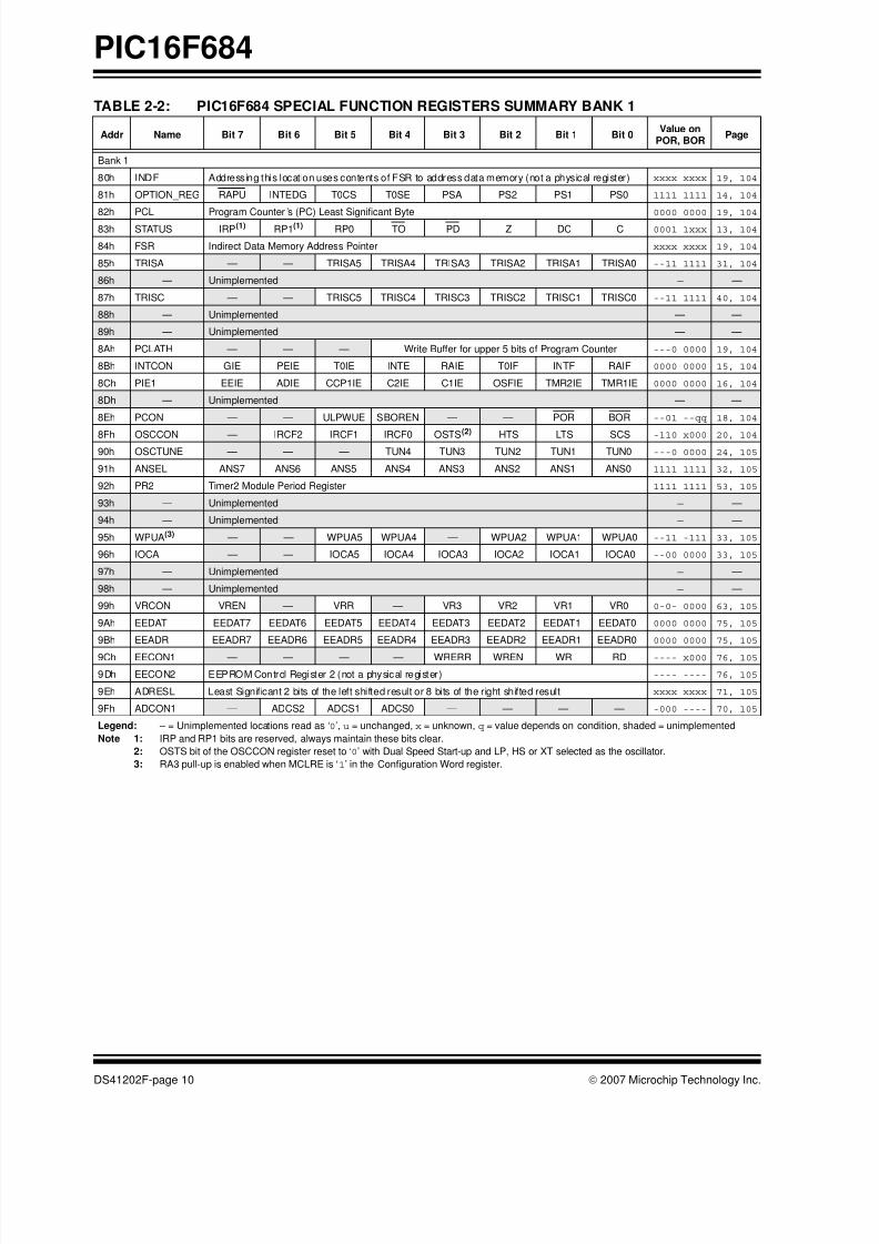
TABLE 2-2: PIC16F684 SPECIAL FUNCTION REGISTERS SUMMARY BANK 1
Addr Name Bit 7 Bit 6 Bit 5 Bit 4 Bit 3 Bit 2 Bit 1 Bit 0Value on
POR, BORPage
Bank 1
80h INDF Addressing this location uses contents of FSR to address data memory (not a physical register) xxxx xxxx 19, 104
81h OPTION_REG RAPU INTEDG T0CS T0SE PSA PS2 PS1 PS0 1111 1111 14, 104
82h PCL Program Counter ’s (PC) Least Significant Byte 0000 0000 19, 104
83h STATUS IRP(1) RP1(1) RP0 TO PD Z DC C 0001 1xxx 13, 104
84h FSR Indirect Data Memory Address Pointer xxxx xxxx 19, 104
85h TRISA — — TRISA5 TRISA4 TRISA3 TRISA2 TRISA1 TRISA0 --11 1111 31, 104
86h — Unimplemented — —
87h TRISC — — TRISC5 TRISC4 TRISC3 TRISC2 TRISC1 TRISC0 --11 1111 40, 104
88h — Unimplemented — —
89h — Unimplemented — —
8Ah PCLATH — — — Write Buffer for upper 5 bits of Program Counter ---0 0000 19, 104
8Bh INTCON GIE PEIE T0IE INTE RAIE T0IF INTF RAIF 0000 0000 15, 104
8Ch PIE1 EEIE ADIE CCP1IE C2IE C1IE OSFIE TMR2IE TMR1IE 0000 0000 16, 104
8Dh — Unimplemented — —
8Eh PCON — — ULPWUE SBOREN — — POR BOR --01 --qq 18, 104
8Fh OSCCON — IRCF2 IRCF1 IRCF0 OSTS(2)
HTS LTS SCS -110 x000 20, 104
90h OSCTUNE — — — TUN4 TUN3 TUN2 TUN1 TUN0 ---0 0000 24, 105
91h ANSEL ANS7 ANS6 ANS5 ANS4 ANS3 ANS2 ANS1 ANS0 1111 1111 32, 105
92h PR2 Timer2 Module Period Register 1111 1111 53, 105
93h — Unimplemented — —
94h — Unimplemented — —
95h WPUA(3) — — WPUA5 WPUA4 — WPUA2 WPUA1 WPUA0 --11 -111 33, 105
96h IOCA — — IOCA5 IOCA4 IOCA3 IOCA2 IOCA1 IOCA0 --00 0000 33, 105
97h — Unimplemented — —
98h — Unimplemented — —
99h VRCON VREN — VRR — VR3 VR2 VR1 VR0 0-0- 0000 63, 105
9Ah EEDAT EEDAT7 EEDAT6 EEDAT5 EEDAT4 EEDAT3 EEDAT2 EEDAT1 EEDAT0 0000 0000 75, 105
9Bh EEADR EEADR7 EEADR6 EEADR5 EEADR4 EEADR3 EEADR2 EEADR1 EEADR0 0000 0000 75, 105
9Ch EECON1 — — — — WRERR WREN WR RD ---- x000 76, 105
9Dh EECON2 EEPROM Control Register 2 (not a physical register) ---- ---- 76, 105
9Eh ADRESL Least Significant 2 bits of the left shifted result or 8 bits of the right shifted result xxxx xxxx 71, 105
9Fh ADCON1 — ADCS2 ADCS1 ADCS0 — — — — -000 ---- 70, 105
Legend: – = Unimplemented locations read as ‘0’, u = unchanged, x = unknown, q = value depends on condition, shaded = unimplemented
Note 1: IRP and RP1 bits are reserved, always maintain these bits clear.
2: OSTS bit of the OSCCON register reset to ‘0’ with Dual Speed Start-up and LP, HS or XT selected as the oscillator.
3: RA3 pull-up is enabled when MCLRE is ‘1’ in the Configuration Word register.
8/10/2019 PIC16F684 Datasheet
http://slidepdf.com/reader/full/pic16f684-datasheet 13/192
© 2007 Microchip Technology Inc. DS41202F-page 11
PIC16F684
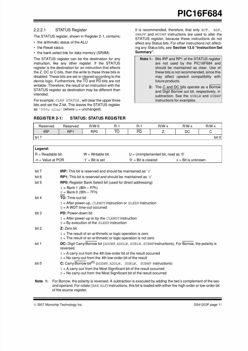
2.2.2.1 STATUS Register
The STATUS register, shown in Register 2-1, contains:
• the arithmetic status of the ALU
• the Reset status
• the bank select bits for data memory (SRAM)
The STATUS register can be the destination for any
instruction, like any other register. If the STATUS
register is the destination for an instruction that affects
the Z, DC or C bits, then the write to these three bits is
disabled. These bits are set or cleared according to the
device logic. Furthermore, the TO and PD bits are not
writable. Therefore, the result of an instruction with the
STATUS register as destination may be different than
intended.
For example, CLRF STATUS, will clear the upper three
bits and set the Z bit. This leaves the STATUS register
as ‘000u u1uu’ (where u = unchanged).
It is recommended, therefore, that only BCF, BSF,
SWAPF and MOVWF instructions are used to alter the
STATUS register, because these instructions do not
affect any Status bits. For other instructions not affect-
ing any Status bits, see Section 13.0 “Instruction Set
Summary”.
Note 1: Bits IRP and RP1 of the STATUS register
are not used by the PIC16F684 and
should be maintained as clear. Use of
these bits is not recommended, since this
may affect upward compatibility with
future products.
2: The C and DC bits operate as a Borrow
and Digit Borrow out bit, respectively, in
subtraction. See the SUBLW and SUBWF
instructions for examples.
REGISTER 2-1: STATUS: STATUS REGISTER
Reserved Reserved R/W-0 R-1 R-1 R/W-x R/W-x R/W-x
IRP RP1 RP0 TO PD Z DC C
bit 7 bit 0
Legend:
R = Readable bit W = Writable bit U = Unimplemented bit, read as ‘0’
-n = Value at POR ‘1’ = Bit is set ‘0’ = Bit is cleared x = Bit is unknown
bit 7 IRP: This bit is reserved and should be maintained as ‘0’
bit 6 RP1: This bit is reserved and should be maintained as ‘0’
bit 5 RP0: Register Bank Select bit (used for direct addressing)
1 = Bank 1 (80h – FFh)
0 = Bank 0 (00h – 7Fh)
bit 4 TO: Time-out bit
1 = After power-up, CLRWDT instruction or SLEEP instruction
0 = A WDT time-out occurred
bit 3 PD: Power-down bit
1 = After power-up or by the CLRWDT instruction
0 = By execution of the SLEEP instruction
bit 2 Z: Zero bit
1 = The result of an arithmetic or logic operation is zero
0 = The result of an arithmetic or logic operation is not zero
bit 1 DC: Digit Carry/Borrow bit ( ADDWF, ADDLW,SUBLW,SUBWF instructions), For Borrow, the polarity is
reversed.
1 = A carry-out from the 4th low-order bit of the result occurred
0 = No carry-out from the 4th low-order bit of the result
bit 0 C: Carry/Borrow bit(1) ( ADDWF, ADDLW, SUBLW, SUBWF instructions)
1 = A carry-out from the Most Significant bit of the result occurred
0 = No carry-out from the Most Significant bit of the result occurred
Note 1: For Borrow, the polarity is reversed. A subtraction is executed by adding the two’s complement of the sec-
ond operand. For rotate (RRF, RLF) instructions, this bit is loaded with either the high-order or low-order bit
of the source register.
8/10/2019 PIC16F684 Datasheet
http://slidepdf.com/reader/full/pic16f684-datasheet 14/192
PIC16F684
DS41202F-page 12 © 2007 Microchip Technology Inc.
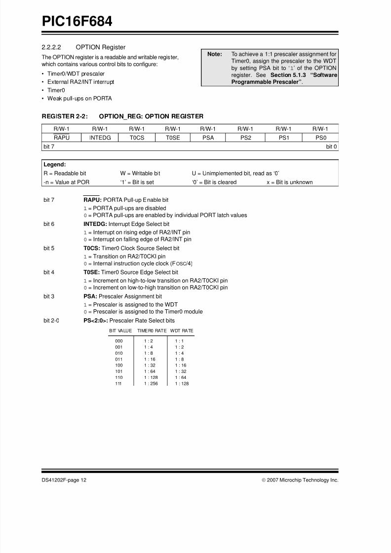
2.2.2.2 OPTION Register
The OPTION register is a readable and writable register,
which contains various control bits to configure:
• Timer0/WDT prescaler
• External RA2/INT interrupt
• Timer0
• Weak pull-ups on PORTA
Note: To achieve a 1:1 prescaler assignment for
Timer0, assign the prescaler to the WDT
by setting PSA bit to ‘1’ of the OPTION
register. See Section 5.1.3 “Software
Programmable Prescaler”.
REGISTER 2-2: OPTION_REG: OPTION REGISTER
R/W-1 R/W-1 R/W-1 R/W-1 R/W-1 R/W-1 R/W-1 R/W-1
RAPU INTEDG T0CS T0SE PSA PS2 PS1 PS0
bit 7 bit 0
Legend:
R = Readable bit W = Writable bit U = Unimplemented bit, read as ‘0’
-n = Value at POR ‘1’ = Bit is set ‘0’ = Bit is cleared x = Bit is unknown
bit 7 RAPU: PORTA Pull-up Enable bit
1 = PORTA pull-ups are disabled
0 = PORTA pull-ups are enabled by individual PORT latch values
bit 6 INTEDG: Interrupt Edge Select bit
1 = Interrupt on rising edge of RA2/INT pin
0 = Interrupt on falling edge of RA2/INT pin
bit 5 T0CS: Timer0 Clock Source Select bit
1 = Transition on RA2/T0CKI pin
0 = Internal instruction cycle clock (FOSC /4)
bit 4 T0SE: Timer0 Source Edge Select bit
1 = Increment on high-to-low transition on RA2/T0CKI pin
0 = Increment on low-to-high transition on RA2/T0CKI pin
bit 3 PSA: Prescaler Assignment bit
1 = Prescaler is assigned to the WDT
0 = Prescaler is assigned to the Timer0 module
bit 2-0 PS<2:0>: Prescaler Rate Select bits
000
001
010
011
100
101
110
111
1 : 2
1 : 4
1 : 8
1 : 16
1 : 32
1 : 64
1 : 128
1 : 256
1 : 1
1 : 2
1 : 4
1 : 8
1 : 16
1 : 32
1 : 64
1 : 128
BIT VALUE TIMER0 RATE WDT RATE
8/10/2019 PIC16F684 Datasheet
http://slidepdf.com/reader/full/pic16f684-datasheet 15/192
© 2007 Microchip Technology Inc. DS41202F-page 13
PIC16F684
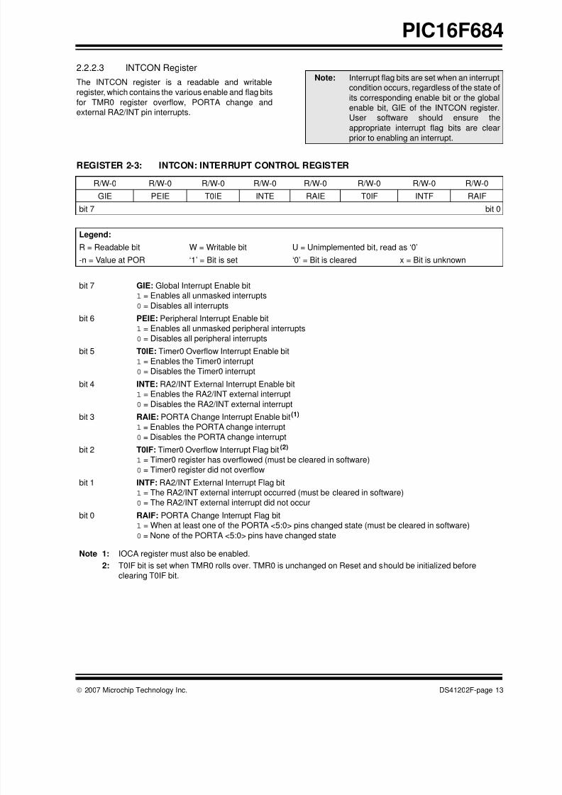
2.2.2.3 INTCON Register
The INTCON register is a readable and writable
register, which contains the various enable and flag bits
for TMR0 register overflow, PORTA change and
external RA2/INT pin interrupts.
Note: Interrupt flag bits are set when an interrupt
condition occurs, regardless of the state of
its corresponding enable bit or the global
enable bit, GIE of the INTCON register.
User software should ensure the
appropriate interrupt flag bits are clear
prior to enabling an interrupt.
REGISTER 2-3: INTCON: INTERRUPT CONTROL REGISTER
R/W-0 R/W-0 R/W-0 R/W-0 R/W-0 R/W-0 R/W-0 R/W-0
GIE PEIE T0IE INTE RAIE T0IF INTF RAIF
bit 7 bit 0
Legend:
R = Readable bit W = Writable bit U = Unimplemented bit, read as ‘0’
-n = Value at POR ‘1’ = Bit is set ‘0’ = Bit is cleared x = Bit is unknown
bit 7 GIE: Global Interrupt Enable bit
1 = Enables all unmasked interrupts
0 = Disables all interrupts
bit 6 PEIE: Peripheral Interrupt Enable bit
1 = Enables all unmasked peripheral interrupts
0 = Disables all peripheral interrupts
bit 5 T0IE: Timer0 Overflow Interrupt Enable bit
1 = Enables the Timer0 interrupt
0 = Disables the Timer0 interrupt
bit 4 INTE: RA2/INT External Interrupt Enable bit
1 = Enables the RA2/INT external interrupt
0 = Disables the RA2/INT external interrupt
bit 3 RAIE: PORTA Change Interrupt Enable bit(1)
1 = Enables the PORTA change interrupt
0 = Disables the PORTA change interrupt
bit 2 T0IF: Timer0 Overflow Interrupt Flag bit(2)
1 = Timer0 register has overflowed (must be cleared in software)
0 = Timer0 register did not overflow
bit 1 INTF: RA2/INT External Interrupt Flag bit
1 = The RA2/INT external interrupt occurred (must be cleared in software)
0 = The RA2/INT external interrupt did not occur
bit 0 RAIF: PORTA Change Interrupt Flag bit
1 = When at least one of the PORTA <5:0> pins changed state (must be cleared in software)
0 = None of the PORTA <5:0> pins have changed state
Note 1: IOCA register must also be enabled.2: T0IF bit is set when TMR0 rolls over. TMR0 is unchanged on Reset and should be initialized before
clearing T0IF bit.
8/10/2019 PIC16F684 Datasheet
http://slidepdf.com/reader/full/pic16f684-datasheet 16/192
PIC16F684
DS41202F-page 14 © 2007 Microchip Technology Inc.
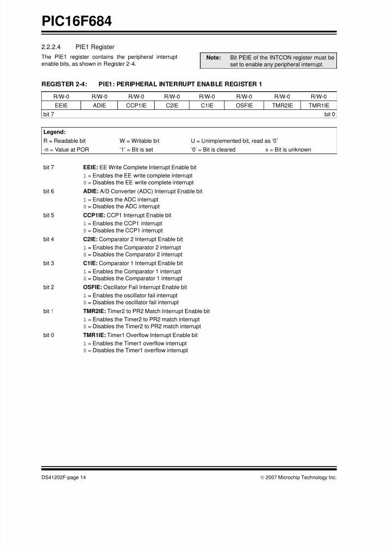
2.2.2.4 PIE1 Register
The PIE1 register contains the peripheral interrupt
enable bits, as shown in Register 2-4.
Note: Bit PEIE of the INTCON register must be
set to enable any peripheral interrupt.
REGISTER 2-4: PIE1: PERIPHERAL INTERRUPT ENABLE REGISTER 1
R/W-0 R/W-0 R/W-0 R/W-0 R/W-0 R/W-0 R/W-0 R/W-0
EEIE ADIE CCP1IE C2IE C1IE OSFIE TMR2IE TMR1IE
bit 7 bit 0
Legend:
R = Readable bit W = Writable bit U = Unimplemented bit, read as ‘0’
-n = Value at POR ‘1’ = Bit is set ‘0’ = Bit is cleared x = Bit is unknown
bit 7 EEIE: EE Write Complete Interrupt Enable bit
1 = Enables the EE write complete interrupt
0 = Disables the EE write complete interrupt
bit 6 ADIE: A/D Converter (ADC) Interrupt Enable bit1 = Enables the ADC interrupt
0 = Disables the ADC interrupt
bit 5 CCP1IE: CCP1 Interrupt Enable bit
1 = Enables the CCP1 interrupt
0 = Disables the CCP1 interrupt
bit 4 C2IE: Comparator 2 Interrupt Enable bit
1 = Enables the Comparator 2 interrupt
0 = Disables the Comparator 2 interrupt
bit 3 C1IE: Comparator 1 Interrupt Enable bit
1 = Enables the Comparator 1 interrupt
0 = Disables the Comparator 1 interrupt
bit 2 OSFIE: Oscillator Fail Interrupt Enable bit1 = Enables the oscillator fail interrupt
0 = Disables the oscillator fail interrupt
bit 1 TMR2IE: Timer2 to PR2 Match Interrupt Enable bit
1 = Enables the Timer2 to PR2 match interrupt
0 = Disables the Timer2 to PR2 match interrupt
bit 0 TMR1IE: Timer1 Overflow Interrupt Enable bit
1 = Enables the Timer1 overflow interrupt
0 = Disables the Timer1 overflow interrupt
8/10/2019 PIC16F684 Datasheet
http://slidepdf.com/reader/full/pic16f684-datasheet 17/192
© 2007 Microchip Technology Inc. DS41202F-page 15
PIC16F684
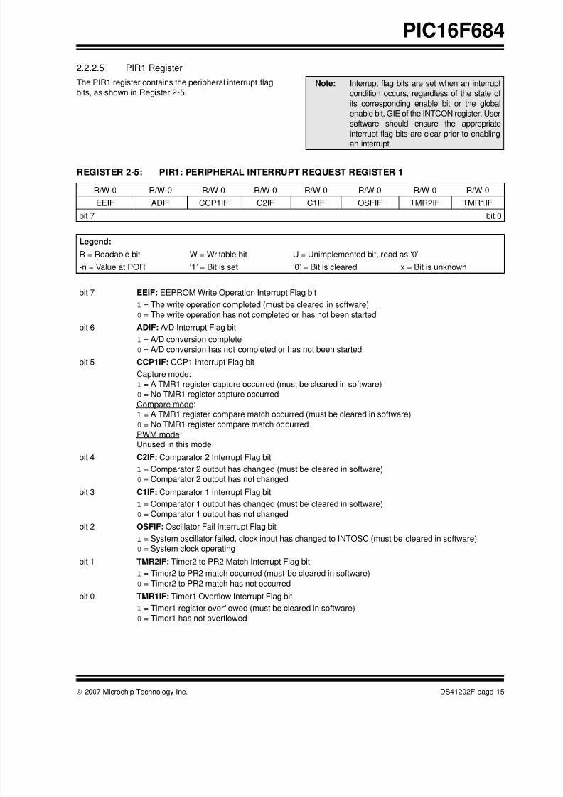
2.2.2.5 PIR1 Register
The PIR1 register contains the peripheral interrupt flag
bits, as shown in Register 2-5.
Note: Interrupt flag bits are set when an interrupt
condition occurs, regardless of the state of
its corresponding enable bit or the global
enable bit, GIE of the INTCON register. User
software should ensure the appropriate
interrupt flag bits are clear prior to enabling
an interrupt.
REGISTER 2-5: PIR1: PERIPHERAL INTERRUPT REQUEST REGISTER 1
R/W-0 R/W-0 R/W-0 R/W-0 R/W-0 R/W-0 R/W-0 R/W-0
EEIF ADIF CCP1IF C2IF C1IF OSFIF TMR2IF TMR1IF
bit 7 bit 0
Legend:
R = Readable bit W = Writable bit U = Unimplemented bit, read as ‘0’
-n = Value at POR ‘1’ = Bit is set ‘0’ = Bit is cleared x = Bit is unknown
bit 7 EEIF: EEPROM Write Operation Interrupt Flag bit
1 = The write operation completed (must be cleared in software)
0 = The write operation has not completed or has not been started
bit 6 ADIF: A/D Interrupt Flag bit
1 = A/D conversion complete
0 = A/D conversion has not completed or has not been started
bit 5 CCP1IF: CCP1 Interrupt Flag bit
Capture mode:
1 = A TMR1 register capture occurred (must be cleared in software)
0 = No TMR1 register capture occurred
Compare mode:
1 = A TMR1 register compare match occurred (must be cleared in software)
0 = No TMR1 register compare match occurred
PWM mode:
Unused in this mode
bit 4 C2IF: Comparator 2 Interrupt Flag bit
1 = Comparator 2 output has changed (must be cleared in software)
0 = Comparator 2 output has not changed
bit 3 C1IF: Comparator 1 Interrupt Flag bit
1 = Comparator 1 output has changed (must be cleared in software)
0 = Comparator 1 output has not changed
bit 2 OSFIF: Oscillator Fail Interrupt Flag bit
1 = System oscillator failed, clock input has changed to INTOSC (must be cleared in software)
0 = System clock operating
bit 1 TMR2IF: Timer2 to PR2 Match Interrupt Flag bit
1 = Timer2 to PR2 match occurred (must be cleared in software)
0 = Timer2 to PR2 match has not occurred
bit 0 TMR1IF: Timer1 Overflow Interrupt Flag bit
1 = Timer1 register overflowed (must be cleared in software)
0 = Timer1 has not overflowed
8/10/2019 PIC16F684 Datasheet
http://slidepdf.com/reader/full/pic16f684-datasheet 18/192
PIC16F684
DS41202F-page 16 © 2007 Microchip Technology Inc.
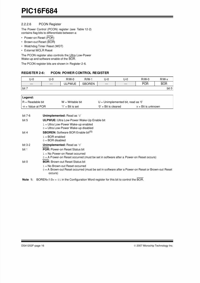
2.2.2.6 PCON Register
The Power Control (PCON) register (see Table 12-2)
contains flag bits to differentiate between a:
• Power-on Reset (POR)
• Brown-out Reset (BOR)
• Watchdog Timer Reset (WDT)
• External MCLR Reset
The PCON register also controls the Ultra Low-Power
Wake-up and software enable of the BOR.
The PCON register bits are shown in Register 2-6.
REGISTER 2-6: PCON: POWER CONTROL REGISTER
U-0 U-0 R/W-0 R/W-1 U-0 U-0 R/W-0 R/W-x
— — ULPWUE SBOREN — — POR BOR
bit 7 bit 0
Legend:
R = Readable bit W = Writable bit U = Unimplemented bit, read as ‘0’
-n = Value at POR ‘1’ = Bit is set ‘0’ = Bit is cleared x = Bit is unknown
bit 7-6 Unimplemented: Read as ‘0’
bit 5 ULPWUE: Ultra Low-Power Wake-Up Enable bit
1 = Ultra Low-Power Wake-up enabled
0 = Ultra Low-Power Wake-up disabled
bit 4 SBOREN: Software BOR Enable bit(1)
1 = BOR enabled
0 = BOR disabled
bit 3-2 Unimplemented: Read as ‘0’
bit 1 POR: Power-on Reset Status bit
1 = No Power-on Reset occurred
0 = A Power-on Reset occurred (must be set in software after a Power-on Reset occurs)
bit 0 BOR: Brown-out Reset Status bit
1 = No Brown-out Reset occurred
0 = A Brown-out Reset occurred (must be set in software after a Power-on Reset or Brown-out Reset
occurs)
Note 1: BOREN<1:0> = 01 in the Configuration Word register for this bit to control the BOR.

8/10/2019 PIC16F684 Datasheet
http://slidepdf.com/reader/full/pic16f684-datasheet 19/192
© 2007 Microchip Technology Inc. DS41202F-page 17
PIC16F684
2.3 PCL and PCLATH
The Program Counter (PC) is 13 bits wide. The low byte
comes from the PCL register, which is a readable and
writable register. The high byte (PC<12:8>) is not directly
readable or writable and comes from PCLATH. On any
Reset, the PC is cleared. Figure 2-3 shows the two
situations for the loading of the PC. The upper examplein Figure 2-3 shows how the PC is loaded on a write to
PCL (PCLATH<4:0> → PCH). The lower example in
Figure 2-3 shows how the PC is loaded during a CALL or
GOTO instruction (PCLATH<4:3> → PCH).
FIGURE 2-3: LOADING OF PC IN
DIFFERENT SITUATIONS
2.3.1 MODIFYING PCL
Executing any instruction with the PCL register as the
destination simultaneously causes the ProgramCounter PC<12:8> bits (PCH) to be replaced by the
contents of the PCLATH register. This allows the entire
contents of the program counter to be changed by first
writing the desired upper 5 bits to the PCLATH register.
Then, when the lower 8 bits are written to the PCL
register, all 13 bits of the program counter will change
to the values contained in the PCLATH register and
those being written to the PCL register.
A computed GOTO is accomplished by adding an offset
to the program counter ( ADDWF PCL). Care should be
exercised when jumping into a look-up table or
program branch table (computed GOTO) by modifying
the PCL register. Assuming that PCLATH is set to the
table start address, if the table length is greater than255 instructions or if the lower 8 bits of the memory
address rolls over from 0xFF to 0x00 in the middle of
the table, then PCLATH must be incremented for each
address rollover that occurs between the table
beginning and the target location within the table.
For more information refer to Application Note AN556,
“Implementing a Table Read ” (DS00556).
2.3.2 STACK
The PIC16F684 Family has an 8-level x 13-bit wide
hardware stack (see Figure 2-1). The stack space is
not part of either program or data space and the Stack
Pointer is not readable or writable. The PC is PUSHed
onto the stack when a CALL instruction is executed or
an interrupt causes a branch. The stack is POPed in
the event of a RETURN, RETLW or a RETFIE
instruction execution. PCLATH is not affected by a
PUSH or POP operation.
The stack operates as a circular buffer. This means that
after the stack has been PUSHed eight times, the ninth
push overwrites the value that was stored from the first
push. The tenth push overwrites the second push (and
so on).
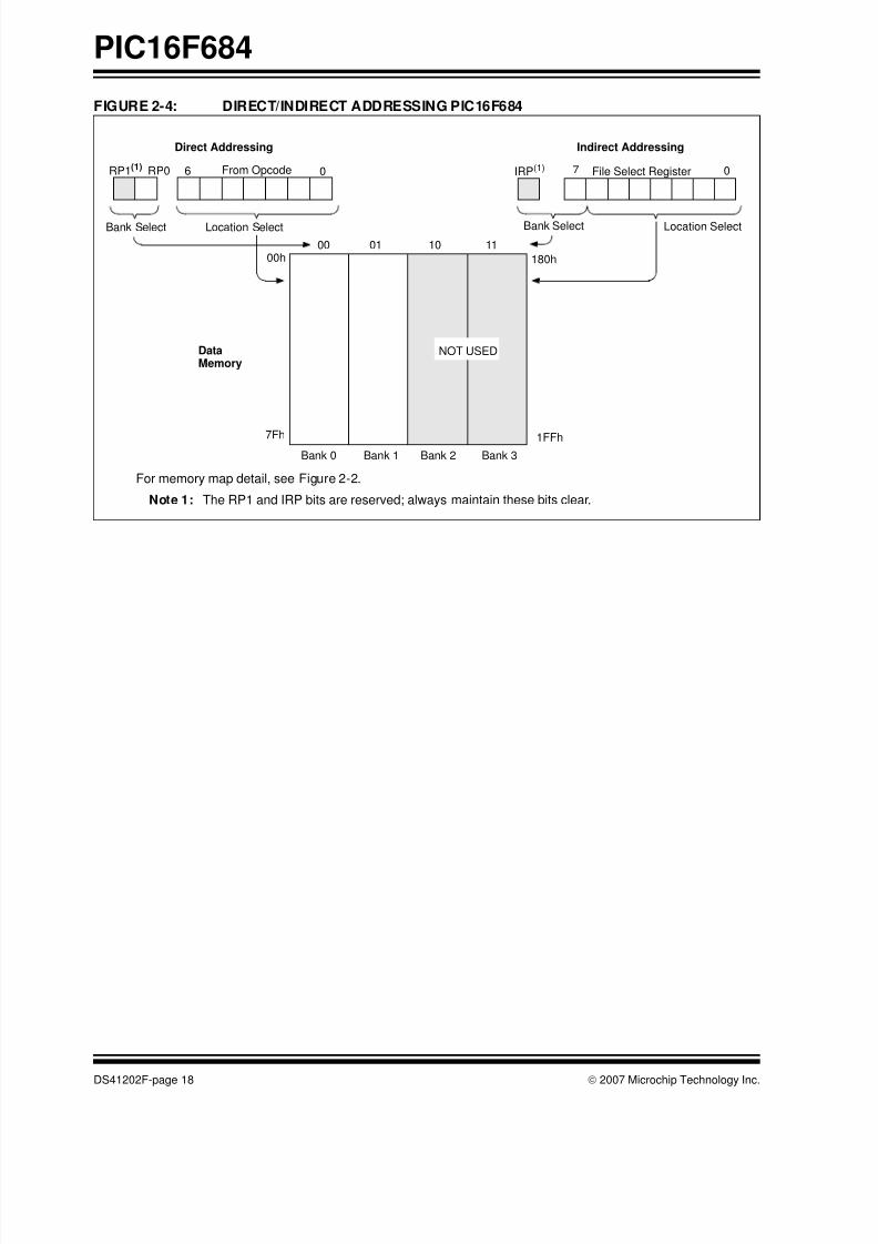
2.4 Indirect Addressing, INDF andFSR Registers
The INDF register is not a physical register. Addressing
the INDF register will cause indirect addressing.
Indirect addressing is possible by using the INDF register.
Any instruction using the INDF register actually accesses
data pointed to by the File Select Register (FSR).
Reading INDF itself indirectly will produce 00h. Writing to
the INDF register indirectly results in a no operation(although Status bits may be affected). An effective 9-bit
address is obtained by concatenating the 8-bit FSR and
the IRP bit of the STATUS register, as shown in
Figure 2-4.
A simple program to clear RAM location 20h-2Fh using
indirect addressing is shown in Example 2-1.
EXAMPLE 2-1: INDIRECT ADDRESSING
PC
12 8 7 0
5PCLATH<4:0>
PCLATH
Instruction with
ALU Result
GOTO, CALL
OPCODE <10:0>
8
PC
12 11 10 0
11PCLATH<4:3>
PCH PCL
8 7
2
PCLATH
PCH PCL
PCL asDestination
Note 1: There are no Status bits to indicate stack
overflow or stack underflow conditions.
2: There are no instructions/mnemonics
called PUSH or POP. These are actions
that occur from the execution of theCALL, RETURN, RETLW and RETFIEinstructions or the vectoring to an
interrupt address.
MOVLW 0x20 ;initialize pointer
MOVWF FSR ;to RAM
NEXT CLRF INDF ;clear INDF register
INCF FSR, f ;inc pointer
BTFSS FSR,4 ;all done?GOTO NEXT ;no clear next
CONTINUE ;yes continue
8/10/2019 PIC16F684 Datasheet
http://slidepdf.com/reader/full/pic16f684-datasheet 20/192
PIC16F684
DS41202F-page 18 © 2007 Microchip Technology Inc.
FIGURE 2-4: DIRECT/INDIRECT ADDRESSING PIC16F684
For memory map detail, see Figure 2-2.
Note 1: The RP1 and IRP bits are reserved; always maintain these bits clear.
DataMemory
Indirect AddressingDirect Addressing
Bank Select Location Select
RP1(1) RP0 6 0From Opcode IRP(1) File Select Register7 0
Bank Select Location Select
00 01 10 11
180h
1FFh
00h
7Fh
Bank 0 Bank 1 Bank 2 Bank 3
NOT USED
8/10/2019 PIC16F684 Datasheet
http://slidepdf.com/reader/full/pic16f684-datasheet 21/192
© 2007 Microchip Technology Inc. DS41202F-page 19
PIC16F684
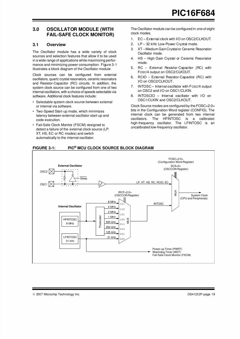
3.0 OSCILLATOR MODULE (WITHFAIL-SAFE CLOCK MONITOR)
3.1 Overview
The Oscillator module has a wide variety of clock
sources and selection features that allow it to be used
in a wide range of applications while maximizing perfor-mance and minimizing power consumption. Figure 3-1
illustrates a block diagram of the Oscillator module.
Clock sources can be configured from external
oscillators, quartz crystal resonators, ceramic resonators
and Resistor-Capacitor (RC) circuits. In addition, the
system clock source can be configured from one of two
internal oscillators, with a choice of speeds selectable via
software. Additional clock features include:
• Selectable system clock source between external
or internal via software.
• Two-Speed Start-up mode, which minimizes
latency between external oscillator start-up and
code execution.
• Fail-Safe Clock Monitor (FSCM) designed to
detect a failure of the external clock source (LP,
XT, HS, EC or RC modes) and switch
automatically to the internal oscillator.
The Oscillator module can be configured in one of eight
clock modes.
1. EC – External clock with I/O on OSC2/CLKOUT.
2. LP – 32 kHz Low-Power Crystal mode.
3. XT – Medium Gain Crystal or Ceramic Resonator
Oscillator mode.
4. HS – High Gain Crystal or Ceramic Resonatormode.
5. RC – External Resistor-Capacitor (RC) with
FOSC /4 output on OSC2/CLKOUT.
6. RCIO – External Resistor-Capacitor (RC) with
I/O on OSC2/CLKOUT.
7. INTOSC – Internal oscillator with FOSC /4 output
on OSC2 and I/O on OSC1/CLKIN.
8. INTOSCIO – Internal oscillator with I/O on
OSC1/CLKIN and OSC2/CLKOUT.
Clock Source modes are configured by the FOSC<2:0>
bits in the Configuration Word register (CONFIG). The
internal clock can be generated from two internal
oscillators. The HFINTOSC is a calibratedhigh-frequency oscillator. The LFINTOSC is an
uncalibrated low-frequency oscillator.
FIGURE 3-1: PIC ® MCU CLOCK SOURCE BLOCK DIAGRAM
(CPU and Peripherals)
OSC1
OSC2
Sleep
External Oscillator
LP, XT, HS, RC, RCIO, EC
System Clock
P o s t s c a l e r
M U X
M U X
8 MHz
4 MHz
2 MHz
1 MHz
500 kHz
125 kHz
250 kHz
IRCF<2:0>
111
110
101
100
011
010
001
00031 kHz
Power-up Timer (PWRT)
FOSC<2:0>(Configuration Word Register)
SCS<0>(OSCCON Register)
Internal Oscillator
(OSCCON Register)
Watchdog Timer (WDT)Fail-Safe Clock Monitor (FSCM)
HFINTOSC
8 MHz
LFINTOSC31 kHz
INTOSC
8/10/2019 PIC16F684 Datasheet
http://slidepdf.com/reader/full/pic16f684-datasheet 22/192
PIC16F684
DS41202F-page 20 © 2007 Microchip Technology Inc.
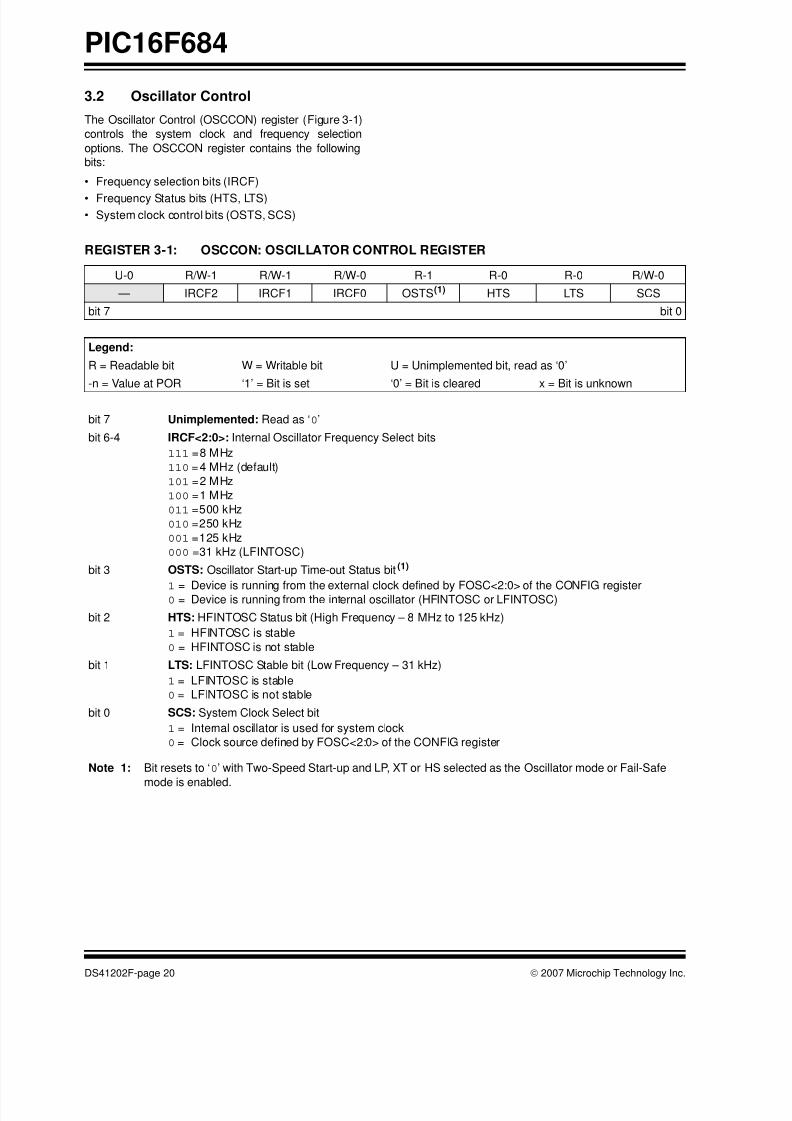
3.2 Oscillator Control
The Oscillator Control (OSCCON) register (Figure 3-1)
controls the system clock and frequency selection
options. The OSCCON register contains the following
bits:
• Frequency selection bits (IRCF)
• Frequency Status bits (HTS, LTS)
• System clock control bits (OSTS, SCS)
REGISTER 3-1: OSCCON: OSCILLATOR CONTROL REGISTER
U-0 R/W-1 R/W-1 R/W-0 R-1 R-0 R-0 R/W-0
— IRCF2 IRCF1 IRCF0 OSTS(1) HTS LTS SCS
bit 7 bit 0
Legend:
R = Readable bit W = Writable bit U = Unimplemented bit, read as ‘0’
-n = Value at POR ‘1’ = Bit is set ‘0’ = Bit is cleared x = Bit is unknown
bit 7 Unimplemented: Read as ‘0’
bit 6-4 IRCF<2:0>: Internal Oscillator Frequency Select bits
111 =8 MHz
110 =4 MHz (default)
101 =2 MHz
100 =1 MHz
011 =500 kHz
010 =250 kHz
001 =125 kHz
000 =31 kHz (LFINTOSC)
bit 3 OSTS: Oscillator Start-up Time-out Status bit(1)
1 = Device is running from the external clock defined by FOSC<2:0> of the CONFIG register0 = Device is running from the internal oscillator (HFINTOSC or LFINTOSC)
bit 2 HTS: HFINTOSC Status bit (High Frequency – 8 MHz to 125 kHz)
1 = HFINTOSC is stable
0 = HFINTOSC is not stable
bit 1 LTS: LFINTOSC Stable bit (Low Frequency – 31 kHz)
1 = LFINTOSC is stable
0 = LFINTOSC is not stable
bit 0 SCS: System Clock Select bit
1 = Internal oscillator is used for system clock
0 = Clock source defined by FOSC<2:0> of the CONFIG register
Note 1: Bit resets to ‘0’ with Two-Speed Start-up and LP, XT or HS selected as the Oscillator mode or Fail-Safe
mode is enabled.
8/10/2019 PIC16F684 Datasheet
http://slidepdf.com/reader/full/pic16f684-datasheet 23/192
© 2007 Microchip Technology Inc. DS41202F-page 21
PIC16F684
3.3 Clock Source Modes
Clock Source modes can be classified as external or
internal.
• External Clock modes rely on external circuitry for
the clock source. Examples are: Oscillator mod-
ules (EC mode), quartz crystal resonators or
ceramic resonators (LP, XT and HS modes) andResistor-Capacitor (RC) mode circuits.
• Internal clock sources are contained internally
within the Oscillator module. The Oscillator
module has two internal oscillators: the 8 MHz
High-Frequency Internal Oscillator (HFINTOSC)
and the 31 kHz Low-Frequency Internal Oscillator
(LFINTOSC).
The system clock can be selected between external or
internal clock sources via the System Clock Select
(SCS) bit of the OSCCON register. See Section 3.6
“Clock Switching” for additional information.
3.4 External Clock Modes
3.4.1 OSCILLATOR START-UP TIMER (OST)
If the Oscillator module is configured for LP, XT or HS
modes, the Oscillator Start-up Timer (OST) counts
1024 oscillations from OSC1. This occurs following a
Power-on Reset (POR) and when the Power-up Timer
(PWRT) has expired (if configured), or a wake-up from
Sleep. During this time, the program counter does not
increment and program execution is suspended. The
OST ensures that the oscillator circuit, using a quartz
crystal resonator or ceramic resonator, has started and
is providing a stable system clock to the Oscillator
module. When switching between clock sources, a
delay is required to allow the new clock to stabilize.
These oscillator delays are shown in Table 3-1.
In order to minimize latency between external oscillator
start-up and code execution, the Two-Speed Clock
Start-up mode can be selected (see Section 3.7
“Two-Speed Clock Start-up Mode”).
TABLE 3-1: OSCILLATOR DELAY EXAMPLES
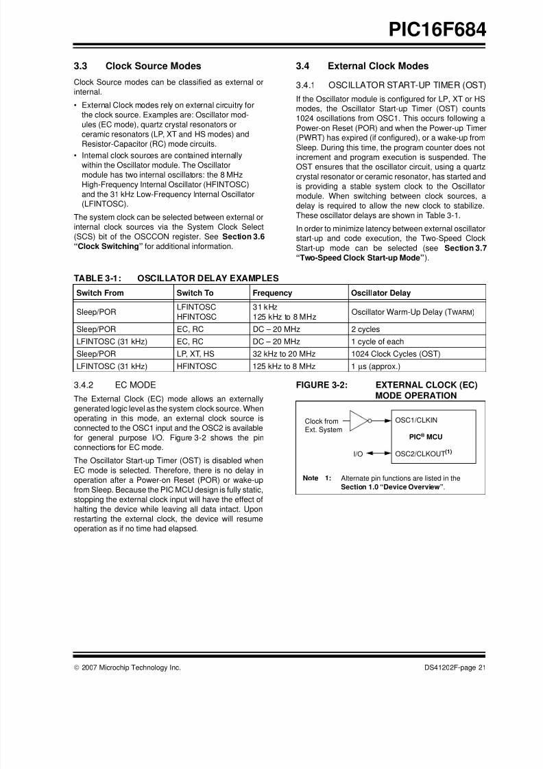
3.4.2 EC MODE
The External Clock (EC) mode allows an externally
generated logic level as the system clock source. When
operating in this mode, an external clock source is
connected to the OSC1 input and the OSC2 is available
for general purpose I/O. Figure 3-2 shows the pin
connections for EC mode.
The Oscillator Start-up Timer (OST) is disabled when
EC mode is selected. Therefore, there is no delay in
operation after a Power-on Reset (POR) or wake-up
from Sleep. Because the PIC MCU design is fully static,
stopping the external clock input will have the effect of
halting the device while leaving all data intact. Upon
restarting the external clock, the device will resume
operation as if no time had elapsed.
FIGURE 3-2: EXTERNAL CLOCK (EC)
MODE OPERATION
Switch From Switch To Frequency Oscillator Delay
Sleep/PORLFINTOSC
HFINTOSC
31 kHz
125 kHz to 8 MHzOscillator Warm-Up Delay (TWARM)
Sleep/POR EC, RC DC – 20 MHz 2 cycles
LFINTOSC (31 kHz) EC, RC DC – 20 MHz 1 cycle of each
Sleep/POR LP, XT, HS 32 kHz to 20 MHz 1024 Clock Cycles (OST)
LFINTOSC (31 kHz) HFINTOSC 125 kHz to 8 MHz 1 µs (approx.)
OSC1/CLKIN
OSC2/CLKOUT(1)I/O
Clock fromExt. System
PIC ® MCU
Note 1: Alternate pin functions are listed in the
Section 1.0 “Device Overview”.

8/10/2019 PIC16F684 Datasheet
http://slidepdf.com/reader/full/pic16f684-datasheet 24/192
PIC16F684
DS41202F-page 22 © 2007 Microchip Technology Inc.
3.4.3 LP, XT, HS MODES
The LP, XT and HS modes support the use of quartz
crystal resonators or ceramic resonators connected to
OSC1 and OSC2 (Figure 3-3). The mode selects a low,
medium or high gain setting of the internal
inverter-amplifier to support various resonator types
and speed.
LP Oscillator mode selects the lowest gain setting of the
internal inverter-amplifier. LP mode current consumption
is the least of the three modes. This mode is designed to
drive only 32.768 kHz tuning-fork type crystals (watch
crystals).
XT Oscillator mode selects the intermediate gain
setting of the internal inverter-amplifier. XT mode
current consumption is the medium of the three modes.
This mode is best suited to drive resonators with a
medium drive level specification.
HS Oscillator mode selects the highest gain setting of the
internal inverter-amplifier. HS mode current consumption
is the highest of the three modes. This mode is best
suited for resonators that require a high drive setting.
Figure 3-3 and Figure 3-4 show typical circuits for
quartz crystal and ceramic resonators, respectively.
FIGURE 3-3: QUARTZ CRYSTALOPERATION (LP, XT ORHS MODE)
FIGURE 3-4: CERAMIC RESONATOROPERATION
(XT OR HS MODE)
Note 1: A series resistor (RS) may be required for
quartz crystals with low drive level.
2: The value of RF varies with the Oscillator mode
selected (typically between 2 MΩ to 10 MΩ).
C1
C2
Quartz
RS(1)
OSC1/CLKIN
RF(2) Sleep
To Internal
Logic
PIC ® MCU
Crystal
OSC2/CLKOUT
Note 1: Quartz crystal characteristics vary according
to type, package and manufacturer. The
user should consult the manufacturer data
sheets for specifications and recommended
application.
2: Always verify oscillator performance over
the VDD and temperature range that isexpected for the application.
3: For oscillator design assistance, reference
the following Microchip Applications Notes:
• AN826, “Crystal Oscillator Basics and
Crystal Selection for rfPIC ® and PIC ®
Devices ” (DS00826)
• AN849, “Basic PIC ® Oscillator Design ”
(DS00849)
• AN943, “Practical PIC ® Oscillator
Analysis and Design ” (DS00943)
• AN949, “Making Your Oscillator Work ”
(DS00949)
Note 1: A series resistor (RS) may be required for
ceramic resonators with low drive level.
2: The value of RF varies with the Oscillator mode
selected (typically between 2 MΩ to 10 MΩ).
3: An additional parallel feedback resistor (RP)
may be required for proper ceramic resonator
operation.
C1
C2 Ceramic RS(1)
OSC1/CLKIN
RF(2) Sleep
To InternalLogic
PIC ® MCU
RP(3)
Resonator
OSC2/CLKOUT

8/10/2019 PIC16F684 Datasheet
http://slidepdf.com/reader/full/pic16f684-datasheet 25/192
© 2007 Microchip Technology Inc. DS41202F-page 23
PIC16F684
3.4.4 EXTERNAL RC MODES
The external Resistor-Capacitor (RC) modes support
the use of an external RC circuit. This allows the
designer maximum flexibility in frequency choice while
keeping costs to a minimum when clock accuracy is not
required. There are two modes: RC and RCIO.
In RC mode, the RC circuit connects to OSC1.OSC2/CLKOUT outputs the RC oscillator frequency
divided by 4. This signal may be used to provide a clock
for external circuitry, synchronization, calibration, test
or other application requirements. Figure 3-5 shows
the external RC mode connections.
FIGURE 3-5: EXTERNAL RC MODES
In RCIO mode, the RC circuit is connected to OSC1.
OSC2 becomes an additional general purpose I/O pin.
The RC oscillator frequency is a function of the supply
voltage, the resistor (REXT) and capacitor (CEXT) values
and the operating temperature. Other factors affecting
the oscillator frequency are:
• threshold voltage variation
• component tolerances
• packaging variations in capacitance
The user also needs to take into account variation due
to tolerance of external RC components used.
3.5 Internal Clock Modes
The Oscillator module has two independent, internal
oscillators that can be configured or selected as the
system clock source.
1. The HFINTOSC (High-Frequency Internal
Oscillator) is factory calibrated and operates at
8 MHz. The frequency of the HFINTOSC can beuser-adjusted via software using the OSCTUNE
register (Register 3-2).
2. The LFINTOSC (Low-Frequency Internal
Oscillator) is uncalibrated and operates at
31 kHz.
The system clock speed can be selected via software
using the Internal Oscillator Frequency Select bits
IRCF<2:0> of the OSCCON register.
The system clock can be selected between external or
internal clock sources via the System Clock Selection
(SCS) bit of the OSCCON register. See Section 3.6
“Clock Switching” for more information.
3.5.1 INTOSC AND INTOSCIO MODES
The INTOSC and INTOSCIO modes configure the
internal oscillators as the system clock source when
the device is programmed using the oscillator selection
or the FOSC<2:0> bits in the Configuration Word
register (CONFIG).
In INTOSC mode, OSC1/CLKIN is available for general
purpose I/O. OSC2/CLKOUT outputs the selected
internal oscillator frequency divided by 4. The CLKOUT
signal may be used to provide a clock for external
circuitry, synchronization, calibration, test or other
application requirements.
In INTOSCIO mode, OSC1/CLKIN and OSC2/CLKOUTare available for general purpose I/O.
3.5.2 HFINTOSC
The High-Frequency Internal Oscillator (HFINTOSC) is
a factory calibrated 8 MHz internal clock source. The
frequency of the HFINTOSC can be altered via
software using the OSCTUNE register (Register 3-2).
The output of the HFINTOSC connects to a postscaler
and multiplexer (see Figure 3-1). One of seven
frequencies can be selected via software using the
IRCF<2:0> bits of the OSCCON register. See
Section 3.5.4 “Frequency Select Bits (IRCF)” for
more information.The HFINTOSC is enabled by selecting any frequency
between 8 MHz and 125 kHz by setting the IRCF<2:0>
bits of the OSCCON register ≠ 000. Then, set the
System Clock Source (SCS) bit of the OSCCON
register to ‘1’ or enable Two-Speed Start-up by setting
the IESO bit in the Configuration Word register
(CONFIG) to ‘1’.
The HF Internal Oscillator (HTS) bit of the OSCCON
register indicates whether the HFINTOSC is stable or not.
OSC2/CLKOUT(1)
CEXT
REXT
PIC ® MCU
OSC1/CLKIN
FOSC /4 or
Internal
Clock
VDD
VSS
Recommended values: 10 kΩ ≤ REXT ≤ 100 kΩ, <3V
3 kΩ ≤ REXT ≤ 100 kΩ, 3-5V
CEXT > 20 pF, 2-5V
Note 1: Alternate pin functions are listed in
Section 1.0 “Device Overview”.
2: Output depends upon RC or RCIO Clock
mode.
I/O(2)

8/10/2019 PIC16F684 Datasheet
http://slidepdf.com/reader/full/pic16f684-datasheet 26/192
PIC16F684
DS41202F-page 24 © 2007 Microchip Technology Inc.
3.5.2.1 OSCTUNE Register
The HFINTOSC is factory calibrated but can be
adjusted in software by writing to the OSCTUNE
register (Register 3-2).
The default value of the OSCTUNE register is ‘0’. The
value is a 5-bit two’s complement number.
When the OSCTUNE register is modified, the
HFINTOSC frequency will begin shifting to the new
frequency. Code execution continues during this shift.
There is no indication that the shift has occurred.
OSCTUNE does not affect the LFINTOSC frequency.
Operation of features that depend on the LFINTOSC
clock source frequency, such as the Power-up Timer
(PWRT), Watchdog Timer (WDT), Fail-Safe ClockMonitor (FSCM) and peripherals, are not affected by the
change in frequency.
REGISTER 3-2: OSCTUNE: OSCILLATOR TUNING REGISTER
U-0 U-0 U-0 R/W-0 R/W-0 R/W-0 R/W-0 R/W-0
— — — TUN4 TUN3 TUN2 TUN1 TUN0
bit 7 bit 0
Legend:
R = Readable bit W = Writable bit U = Unimplemented bit, read as ‘0’
-n = Value at POR ‘1’ = Bit is set ‘0’ = Bit is cleared x = Bit is unknown
bit 7-5 Unimplemented: Read as ‘0’
bit 4-0 TUN<4:0>: Frequency Tuning bits
01111 = Maximum frequency
01110 =
•
•
•
00001 =
00000 = Oscillator module is running at the calibrated frequency.
11111 =
•
•
•
10000 = Minimum frequency
8/10/2019 PIC16F684 Datasheet
http://slidepdf.com/reader/full/pic16f684-datasheet 27/192
© 2007 Microchip Technology Inc. DS41202F-page 25
PIC16F684
3.5.3 LFINTOSC
The Low-Frequency Internal Oscillator (LFINTOSC) is
an uncalibrated 31 kHz internal clock source.
The output of the LFINTOSC connects to a postscaler
and multiplexer (see Figure 3-1). Select 31 kHz, via
software, using the IRCF<2:0> bits of the OSCCON
register. See Section 3.5.4 “Frequency Select Bits(IRCF)” for more information. The LFINTOSC is also the
frequency for the Power-up Timer (PWRT), Watchdog
Timer (WDT) and Fail-Safe Clock Monitor (FSCM).
The LFINTOSC is enabled by selecting 31 kHz
(IRCF<2:0> bits of the OSCCON register = 000) as the
system clock source (SCS bit of the OSCCON
register = 1), or when any of the following are enabled:
• Two-Speed Start-up IESO bit of the Configuration
Word register = 1 and IRCF<2:0> bits of the
OSCCON register = 000
• Power-up Timer (PWRT)
• Watchdog Timer (WDT)
• Fail-Safe Clock Monitor (FSCM)
The LF Internal Oscillator (LTS) bit of the OSCCON
register indicates whether the LFINTOSC is stable or
not.
3.5.4 FREQUENCY SELECT BITS (IRCF)
The output of the 8 MHz HFINTOSC and 31 kHz
LFINTOSC connects to a postscaler and multiplexer
(see Figure 3-1). The Internal Oscillator Frequency
Select bits IRCF<2:0> of the OSCCON register select
the frequency output of the internal oscillators. One of
eight frequencies can be selected via software:
• 8 MHz
• 4 MHz (Default after Reset)
• 2 MHz
• 1 MHz
• 500 kHz
• 250 kHz
• 125 kHz
• 31 kHz (LFINTOSC)
3.5.5 HFINTOSC AND LFINTOSC CLOCK
SWITCH TIMING
When switching between the LFINTOSC and the
HFINTOSC, the new oscillator may already be shut
down to save power (see Figure 3-6). If this is the case,
there is a delay after the IRCF<2:0> bits of the
OSCCON register are modified before the frequency
selection takes place. The LTS and HTS bits of the
OSCCON register will reflect the current active status
of the LFINTOSC and HFINTOSC oscillators. The
timing of a frequency selection is as follows:
1. IRCF<2:0> bits of the OSCCON register are
modified.
2. If the new clock is shut down, a clock start-up
delay is started.
3. Clock switch circuitry waits for a falling edge of
the current clock.
4. CLKOUT is held low and the clock switch
circuitry waits for a rising edge in the new clock.
5. CLKOUT is now connected with the new clock.LTS and HTS bits of the OSCCON register are
updated as required.
6. Clock switch is complete.
See Figure 3-1 for more details.
If the internal oscillator speed selected is between
8 MHz and 125 kHz, there is no start-up delay before
the new frequency is selected. This is because the old
and new frequencies are derived from the HFINTOSC
via the postscaler and multiplexer.
Start-up delay specifications are located in the
oscillator tables of Section 15.0 “Electrical
Specifications”.
Note: Following any Reset, the IRCF<2:0> bits of
the OSCCON register are set to ‘110’ and
the frequency selection is set to 4 MHz.
The user can modify the IRCF bits to
select a different frequency.
8/10/2019 PIC16F684 Datasheet
http://slidepdf.com/reader/full/pic16f684-datasheet 28/192
PIC16F684
DS41202F-page 26 © 2007 Microchip Technology Inc.
FIGURE 3-6: INTERNAL OSCILLATOR SWITCH TIMING
HFINTOSC
LFINTOSC
IRCF <2:0>
System Clock
HFINTOSC
LFINTOSC
IRCF <2:0>
System Clock
≠ 0 = 0
≠ 0 = 0
Start-up Time 2-cycle Sync Running
2-cycle Sync Running
HFINTOSC LFINTOSC (FSCM and WDT disabled)
HFINTOSC LFINTOSC (Either FSCM or WDT enabled)
LFINTOSC
HFINTOSC
IRCF <2:0>
System Clock
= 0 ¼ 0
Start-up Time 2-cycle Sync Running
LFINTOSC HFINTOSCLFINTOSC turns off unless WDT or FSCM is enabled
8/10/2019 PIC16F684 Datasheet
http://slidepdf.com/reader/full/pic16f684-datasheet 29/192
© 2007 Microchip Technology Inc. DS41202F-page 27
PIC16F684
3.6 Clock Switching
The system clock source can be switched between
external and internal clock sources via software using
the System Clock Select (SCS) bit of the OSCCON
register.
3.6.1 SYSTEM CLOCK SELECT (SCS) BIT
The System Clock Select (SCS) bit of the OSCCON
register selects the system clock source that is used for
the CPU and peripherals.
• When the SCS bit of the OSCCON register = 0,
the system clock source is determined by
configuration of the FOSC<2:0> bits in the
Configuration Word register (CONFIG).
• When the SCS bit of the OSCCON register = 1,
the system clock source is chosen by the internal
oscillator frequency selected by the IRCF<2:0>
bits of the OSCCON register. After a Reset, the
SCS bit of the OSCCON register is always
cleared.
3.6.2 OSCILLATOR START-UP TIME-OUT
STATUS (OSTS) BIT
The Oscillator Start-up Time-out Status (OSTS) bit of
the OSCCON register indicates whether the system
clock is running from the external clock source, as
defined by the FOSC<2:0> bits in the Configuration
Word register (CONFIG), or from the internal clock
source. In particular, OSTS indicates that the Oscillator
Start-up Timer (OST) has timed out for LP, XT or HS
modes.
3.7 Two-Speed Clock Start-up Mode
Two-Speed Start-up mode provides additional power
savings by minimizing the latency between external
oscillator start-up and code execution. In applications
that make heavy use of the Sleep mode, Two-Speed
Start-up will remove the external oscillator start-up
time from the time spent awake and can reduce the
overall power consumption of the device.
This mode allows the application to wake-up from
Sleep, perform a few instructions using the INTOSC
as the clock source and go back to Sleep without
waiting for the primary oscillator to become stable.
When the Oscillator module is configured for LP, XT or
HS modes, the Oscillator Start-up Timer (OST) is
enabled (see Section 3.4.1 “Oscillator Start-up Timer
(OST)”). The OST will suspend program execution until
1024 oscillations are counted. Two-Speed Start-up
mode minimizes the delay in code execution by
operating from the internal oscillator as the OST is
counting. When the OST count reaches 1024 and theOSTS bit of the OSCCON register is set, program
execution switches to the external oscillator.
3.7.1 TWO-SPEED START-UP MODECONFIGURATION
Two-Speed Start-up mode is configured by the
following settings:
• IESO (of the Configuration Word register) = 1;
Internal/External Switchover bit (Two-Speed
Start-up mode enabled).
• SCS (of the OSCCON register) = 0.
• FOSC<2:0> bits in the Configuration Word
register (CONFIG) configured for LP, XT or HSmode.
Two-Speed Start-up mode is entered after:
• Power-on Reset (POR) and, if enabled, after
Power-up Timer (PWRT) has expired, or
• Wake-up from Sleep.
If the external clock oscillator is configured to be
anything other than LP, XT or HS mode, then
Two-Speed Start-up is disabled. This is because the
external clock oscillator does not require any
stabilization time after POR or an exit from Sleep.
3.7.2 TWO-SPEED START-UPSEQUENCE
1. Wake-up from Power-on Reset or Sleep.
2. Instructions begin execution by the internal
oscillator at the frequency set in the IRCF<2:0>
bits of the OSCCON register.
3. OST enabled to count 1024 clock cycles.
4. OST timed out, wait for falling edge of the
internal oscillator.
5. OSTS is set.
6. System clock held low until the next falling edge
of new clock (LP, XT or HS mode).
7. System clock is switched to external clock
source.
Note: Any automatic clock switch, which may
occur from Two-Speed Start-up or Fail-Safe
Clock Monitor, does not update the SCS bit
of the OSCCON register. The user can
monitor the OSTS bit of the OSCCON
register to determine the current system
clock source.
Note: Executing a SLEEP instruction will abort
the oscillator start-up time and will cause
the OSTS bit of the OSCCON register to
remain clear.
8/10/2019 PIC16F684 Datasheet
http://slidepdf.com/reader/full/pic16f684-datasheet 30/192
PIC16F684
DS41202F-page 28 © 2007 Microchip Technology Inc.
3.7.3 CHECKING TWO-SPEED CLOCK
STATUS
Checking the state of the OSTS bit of the OSCCON
register will confirm if the microcontroller is running
from the external clock source, as defined by the
FOSC<2:0> bits in the Configuration Word register
(CONFIG), or the internal oscillator.
FIGURE 3-7: TWO-SPEED START-UP
0 1 1022 1023
PC + 1
TOSTT
HFINTOSC
OSC1
OSC2
Program Counter
System Clock
PC - N PC
8/10/2019 PIC16F684 Datasheet
http://slidepdf.com/reader/full/pic16f684-datasheet 31/192
© 2007 Microchip Technology Inc. DS41202F-page 29
PIC16F684
3.8 Fail-Safe Clock Monitor
The Fail-Safe Clock Monitor (FSCM) allows the device
to continue operating should the external oscillator fail.
The FSCM can detect oscillator failure any time after
the Oscillator Start-up Timer (OST) has expired. The
FSCM is enabled by setting the FCMEN bit in the
Configuration Word register (CONFIG). The FSCM isapplicable to all external oscillator modes (LP, XT, HS,
EC, RC and RCIO).
FIGURE 3-8: FSCM BLOCK DIAGRAM
3.8.1 FAIL-SAFE DETECTION
The FSCM module detects a failed oscillator by
comparing the external oscillator to the FSCM sample
clock. The sample clock is generated by dividing the
LFINTOSC by 64. See Figure 3-8. Inside the fail
detector block is a latch. The external clock sets the
latch on each falling edge of the external clock. The
sample clock clears the latch on each rising edge of the
sample clock. A failure is detected when an entire
half-cycle of the sample clock elapses before the
primary clock goes low.
3.8.2 FAIL-SAFE OPERATION
When the external clock fails, the FSCM switches the
device clock to an internal clock source and sets the bit
flag OSFIF of the PIR1 register. Setting this flag will
generate an interrupt if the OSFIE bit of the PIE1
register is also set. The device firmware can then take
steps to mitigate the problems that may arise from a
failed clock. The system clock will continue to be
sourced from the internal clock source until the devicefirmware successfully restarts the external oscillator
and switches back to external operation.
The internal clock source chosen by the FSCM is
determined by the IRCF<2:0> bits of the OSCCON
register. This allows the internal oscillator to be
configured before a failure occurs.
3.8.3 FAIL-SAFE CONDITION CLEARING
The Fail-Safe condition is cleared after a Reset,
executing a SLEEP instruction or toggling the SCS bit
of the OSCCON register. When the SCS bit is toggled,
the OST is restarted. While the OST is running, the
device continues to operate from the INTOSC selected
in OSCCON. When the OST times out, the Fail-Safe
condition is cleared and the device will be operating
from the external clock source. The Fail-Safe condition
must be cleared before the OSFIF flag can be cleared.
3.8.4 RESET OR WAKE-UP FROM SLEEP
The FSCM is designed to detect an oscillator failure
after the Oscillator Start-up Timer (OST) has expired.
The OST is used after waking up from Sleep and after
any type of Reset. The OST is not used with the EC or
RC Clock modes so that the FSCM will be active as
soon as the Reset or wake-up has completed. When
the FSCM is enabled, the Two-Speed Start-up is also
enabled. Therefore, the device will always be executing
code while the OST is operating.
External
LFINTOSC÷ 64
S
R
Q
31 kHz(~32 µs)
488 Hz(~2 ms)
Clock Monitor
Latch
Clock
Failure
Detected
Oscillator
Clock
Q
Sample ClockNote: Due to the wide range of oscillator start-up
times, the Fail-Safe circuit is not active
during oscillator start-up (i.e., after exiting
Reset or Sleep). After an appropriate
amount of time, the user should check the
OSTS bit of the OSCCON register to verify
the oscillator start-up and that the system
clock switchover has successfully
completed.

8/10/2019 PIC16F684 Datasheet
http://slidepdf.com/reader/full/pic16f684-datasheet 32/192
PIC16F684
DS41202F-page 30 © 2007 Microchip Technology Inc.
FIGURE 3-9: FSCM TIMING DIAGRAM
TABLE 3-2: SUMMARY OF REGISTERS ASSOCIATED WITH CLOCK SOURCES
OSCFIF
SystemClock
Output
Sample Clock
FailureDetected
OscillatorFailure
Note: The system clock is normally at a much higher frequency than the sample clock. The relative frequencies in
this example have been chosen for clarity.
(Q)
Test Test Test
Clock Monitor Output
Name Bit 7 Bit 6 Bit 5 Bit 4 Bit 3 Bit 2 Bit 1 Bit 0Value on:
POR, BOR
Value on
all other
Resets(1)
CONFIG(2) CPD CP MCLRE PWRTE WDTE FOSC2 FOSC1 FOSC0 — —
OSCCON — IRCF2 IRCF1 IRCF0 OSTS HTS LTS SCS -110 x000 -110 x000
OSCTUNE — — — TUN4 TUN3 TUN2 TUN1 TUN0 ---0 0000 ---u uuuu
PIE1 EEIE ADIE CCP1IE C2IE C1IE OSFIE TMR2IE TMR1IE 0000 0000 0000 0000
PIR1 EEIF ADIF CCP1IF C2IF C1IF OSFIF TMR2IF TMR1IF 0000 0000 0000 0000
Legend: x = unknown, u = unchanged, – = unimplemented locations read as ‘0’. Shaded cells are not used by oscillators.
Note 1: Other (non Power-up) Resets include MCLR Reset and Watchdog Timer Reset during normal operation.
2: See Configuration Word register (Register 12-1) for operation of all register bits.
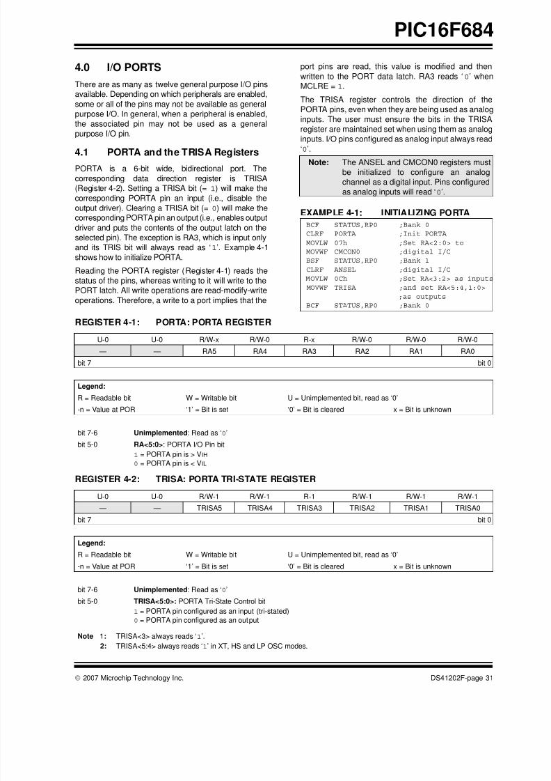
8/10/2019 PIC16F684 Datasheet
http://slidepdf.com/reader/full/pic16f684-datasheet 33/192
© 2007 Microchip Technology Inc. DS41202F-page 31
PIC16F684
4.0 I/O PORTS
There are as many as twelve general purpose I/O pins
available. Depending on which peripherals are enabled,
some or all of the pins may not be available as general
purpose I/O. In general, when a peripheral is enabled,
the associated pin may not be used as a general
purpose I/O pin.
4.1 PORTA and the TRISA Registers
PORTA is a 6-bit wide, bidirectional port. The
corresponding data direction register is TRISA
(Register 4-2). Setting a TRISA bit (= 1) will make the
corresponding PORTA pin an input (i.e., disable the
output driver). Clearing a TRISA bit (= 0) will make the
corresponding PORTA pin an output (i.e., enables output
driver and puts the contents of the output latch on the
selected pin). The exception is RA3, which is input only
and its TRIS bit will always read as ‘1’. Example 4-1
shows how to initialize PORTA.
Reading the PORTA register (Register 4-1) reads thestatus of the pins, whereas writing to it will write to the
PORT latch. All write operations are read-modify-write
operations. Therefore, a write to a port implies that the
port pins are read, this value is modified and then
written to the PORT data latch. RA3 reads ‘0’ when
MCLRE = 1.
The TRISA register controls the direction of the
PORTA pins, even when they are being used as analog
inputs. The user must ensure the bits in the TRISA
register are maintained set when using them as analog
inputs. I/O pins configured as analog input always read‘0’.
EXAMPLE 4-1: INITIALIZING PORTA
Note: The ANSEL and CMCON0 registers must
be initialized to configure an analog
channel as a digital input. Pins configured
as analog inputs will read ‘0’.
BCF STATUS,RP0 ;Bank 0
CLRF PORTA ;Init PORTA
MOVLW 07h ;Set RA<2:0> to
MOVWF CMCON0 ;digital I/O
BSF STATUS,RP0 ;Bank 1
CLRF ANSEL ;digital I/O
MOVLW 0Ch ;Set RA<3:2> as inputs
MOVWF TRISA ;and set RA<5:4,1:0>
;as outputs
BCF STATUS,RP0 ;Bank 0
REGISTER 4-1: PORTA: PORTA REGISTER
U-0 U-0 R/W-x R/W-0 R-x R/W-0 R/W-0 R/W-0
— — RA5 RA4 RA3 RA2 RA1 RA0
bit 7 bit 0
Legend:
R = Readable bit W = Writable bit U = Unimplemented bit, read as ‘0’
-n = Value at POR ‘1’ = Bit is set ‘0’ = Bit is cleared x = Bit is unknown
bit 7-6 Unimplemented: Read as ‘0’
bit 5-0 RA<5:0>: PORTA I/O Pin bit
1 = PORTA pin is > VIH
0 = PORTA pin is < VIL
REGISTER 4-2: TRISA: PORTA TRI-STATE REGISTER
U-0 U-0 R/W-1 R/W-1 R-1 R/W-1 R/W-1 R/W-1
— — TRISA5 TRISA4 TRISA3 TRISA2 TRISA1 TRISA0
bit 7 bit 0
Legend:
R = Readable bit W = Writable bit U = Unimplemented bit, read as ‘0’
-n = Value at POR ‘1’ = Bit is set ‘0’ = Bit is cleared x = Bit is unknown
bit 7-6 Unimplemented: Read as ‘0’
bit 5-0 TRISA<5:0>: PORTA Tri-State Control bit
1 = PORTA pin configured as an input (tri-stated)
0 = PORTA pin configured as an output
Note 1: TRISA<3> always reads ‘1’.
2: TRISA<5:4> always reads ‘1’ in XT, HS and LP OSC modes.
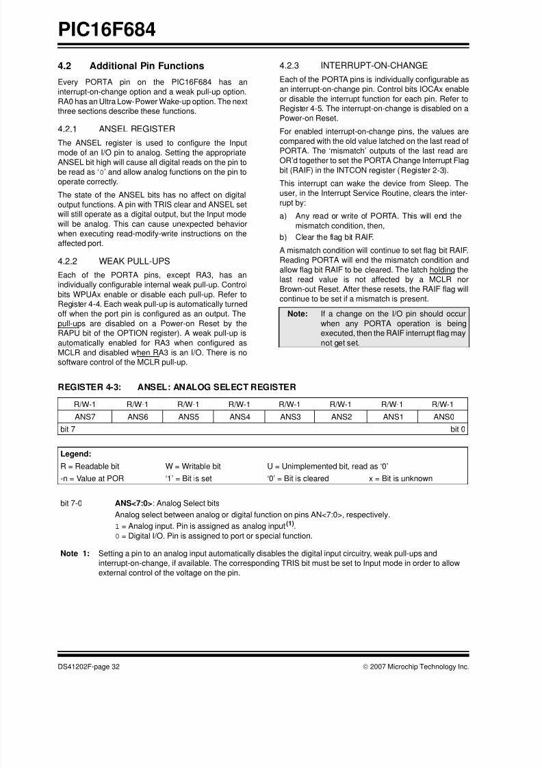
8/10/2019 PIC16F684 Datasheet
http://slidepdf.com/reader/full/pic16f684-datasheet 34/192
PIC16F684
DS41202F-page 32 © 2007 Microchip Technology Inc.
4.2 Additional Pin Functions
Every PORTA pin on the PIC16F684 has an
interrupt-on-change option and a weak pull-up option.
RA0 has an Ultra Low-Power Wake-up option. The next
three sections describe these functions.
4.2.1 ANSEL REGISTER
The ANSEL register is used to configure the Input
mode of an I/O pin to analog. Setting the appropriate
ANSEL bit high will cause all digital reads on the pin to
be read as ‘0’ and allow analog functions on the pin to
operate correctly.
The state of the ANSEL bits has no affect on digital
output functions. A pin with TRIS clear and ANSEL set
will still operate as a digital output, but the Input mode
will be analog. This can cause unexpected behavior
when executing read-modify-write instructions on the
affected port.
4.2.2 WEAK PULL-UPS
Each of the PORTA pins, except RA3, has an
individually configurable internal weak pull-up. Control
bits WPUAx enable or disable each pull-up. Refer to
Register 4-4. Each weak pull-up is automatically turned
off when the port pin is configured as an output. The
pull-ups are disabled on a Power-on Reset by the
RAPU bit of the OPTION register). A weak pull-up is
automatically enabled for RA3 when configured as
MCLR and disabled when RA3 is an I/O. There is no
software control of the MCLR pull-up.
4.2.3 INTERRUPT-ON-CHANGE
Each of the PORTA pins is individually configurable as
an interrupt-on-change pin. Control bits IOCAx enable
or disable the interrupt function for each pin. Refer to
Register 4-5. The interrupt-on-change is disabled on a
Power-on Reset.
For enabled interrupt-on-change pins, the values arecompared with the old value latched on the last read of
PORTA. The ‘mismatch’ outputs of the last read are
OR’d together to set the PORTA Change Interrupt Flag
bit (RAIF) in the INTCON register (Register 2-3).
This interrupt can wake the device from Sleep. The
user, in the Interrupt Service Routine, clears the inter-
rupt by:
a) Any read or write of PORTA. This will end the
mismatch condition, then,
b) Clear the flag bit RAIF.
A mismatch condition will continue to set flag bit RAIF.
Reading PORTA will end the mismatch condition and
allow flag bit RAIF to be cleared. The latch holding thelast read value is not affected by a MCLR nor
Brown-out Reset. After these resets, the RAIF flag will
continue to be set if a mismatch is present.
Note: If a change on the I/O pin should occur
when any PORTA operation is being
executed, then the RAIF interrupt flag may
not get set.
REGISTER 4-3: ANSEL: ANALOG SELECT REGISTER
R/W-1 R/W-1 R/W-1 R/W-1 R/W-1 R/W-1 R/W-1 R/W-1
ANS7 ANS6 ANS5 ANS4 ANS3 ANS2 ANS1 ANS0
bit 7 bit 0
Legend:
R = Readable bit W = Writable bit U = Unimplemented bit, read as ‘0’
-n = Value at POR ‘1’ = Bit is set ‘0’ = Bit is cleared x = Bit is unknown
bit 7-0 ANS<7:0>: Analog Select bits
Analog select between analog or digital function on pins AN<7:0>, respectively.
1 = Analog input. Pin is assigned as analog input(1).
0 = Digital I/O. Pin is assigned to port or special function.
Note 1: Setting a pin to an analog input automatically disables the digital input circuitry, weak pull-ups and
interrupt-on-change, if available. The corresponding TRIS bit must be set to Input mode in order to allow
external control of the voltage on the pin.
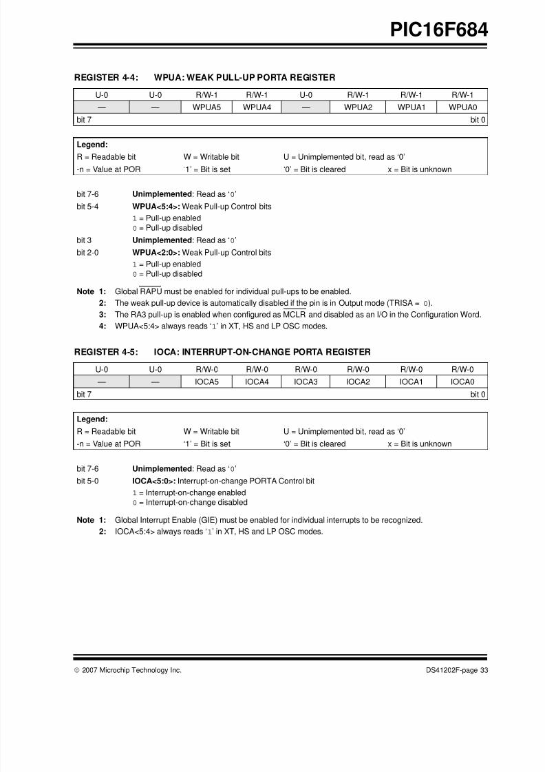
8/10/2019 PIC16F684 Datasheet
http://slidepdf.com/reader/full/pic16f684-datasheet 35/192
© 2007 Microchip Technology Inc. DS41202F-page 33
PIC16F684
REGISTER 4-4: WPUA: WEAK PULL-UP PORTA REGISTER
U-0 U-0 R/W-1 R/W-1 U-0 R/W-1 R/W-1 R/W-1
— — WPUA5 WPUA4 — WPUA2 WPUA1 WPUA0
bit 7 bit 0
Legend:
R = Readable bit W = Writable bit U = Unimplemented bit, read as ‘0’
-n = Value at POR ‘1’ = Bit is set ‘0’ = Bit is cleared x = Bit is unknown
bit 7-6 Unimplemented: Read as ‘0’
bit 5-4 WPUA<5:4>: Weak Pull-up Control bits
1 = Pull-up enabled
0 = Pull-up disabled
bit 3 Unimplemented: Read as ‘0’
bit 2-0 WPUA<2:0>: Weak Pull-up Control bits
1 = Pull-up enabled
0 = Pull-up disabled
Note 1: Global RAPU must be enabled for individual pull-ups to be enabled.
2: The weak pull-up device is automatically disabled if the pin is in Output mode (TRISA = 0).
3: The RA3 pull-up is enabled when configured as MCLR and disabled as an I/O in the Configuration Word.
4: WPUA<5:4> always reads ‘1’ in XT, HS and LP OSC modes.
REGISTER 4-5: IOCA: INTERRUPT-ON-CHANGE PORTA REGISTER
U-0 U-0 R/W-0 R/W-0 R/W-0 R/W-0 R/W-0 R/W-0
— — IOCA5 IOCA4 IOCA3 IOCA2 IOCA1 IOCA0
bit 7 bit 0
Legend:
R = Readable bit W = Writable bit U = Unimplemented bit, read as ‘0’
-n = Value at POR ‘1’ = Bit is set ‘0’ = Bit is cleared x = Bit is unknown
bit 7-6 Unimplemented: Read as ‘0’
bit 5-0 IOCA<5:0>: Interrupt-on-change PORTA Control bit
1 = Interrupt-on-change enabled
0 = Interrupt-on-change disabled
Note 1: Global Interrupt Enable (GIE) must be enabled for individual interrupts to be recognized.
2: IOCA<5:4> always reads ‘1’ in XT, HS and LP OSC modes.
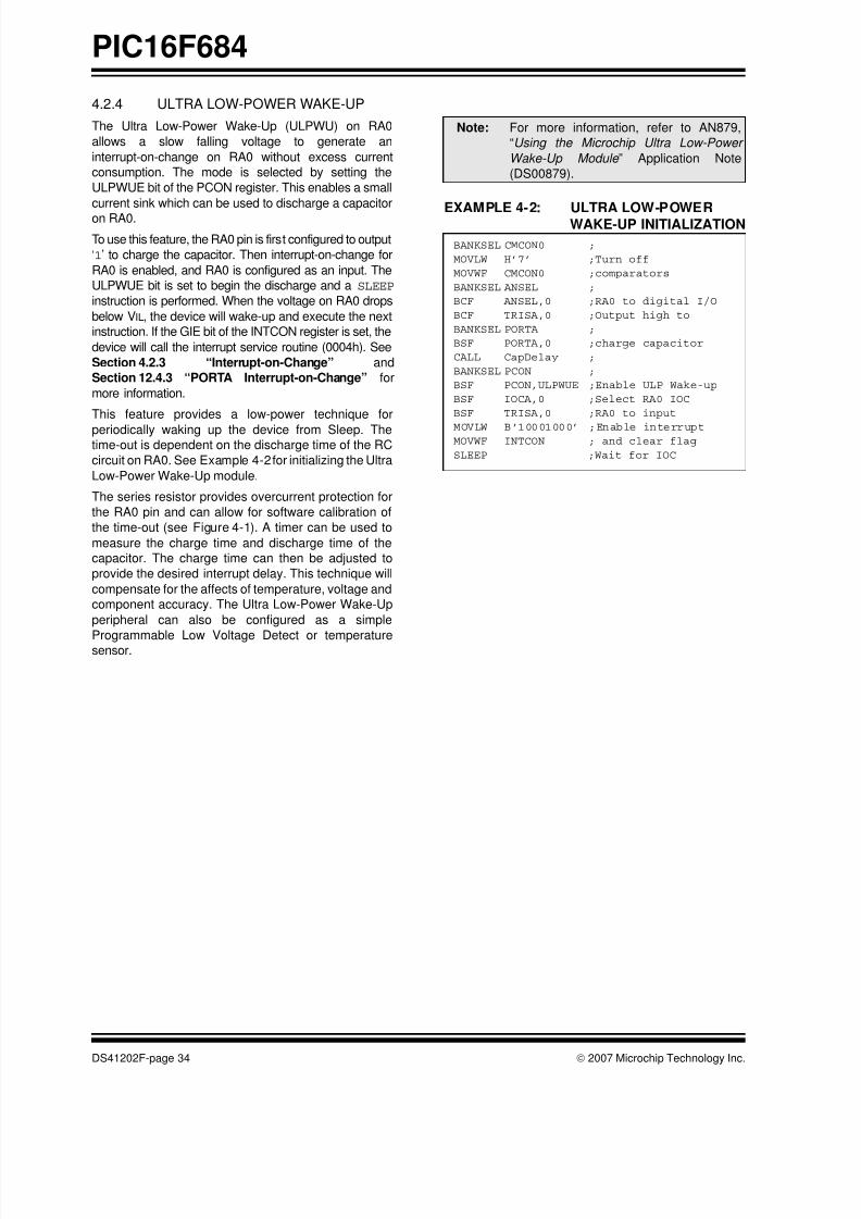
8/10/2019 PIC16F684 Datasheet
http://slidepdf.com/reader/full/pic16f684-datasheet 36/192
PIC16F684
DS41202F-page 34 © 2007 Microchip Technology Inc.
4.2.4 ULTRA LOW-POWER WAKE-UP
The Ultra Low-Power Wake-Up (ULPWU) on RA0
allows a slow falling voltage to generate an
interrupt-on-change on RA0 without excess current
consumption. The mode is selected by setting the
ULPWUE bit of the PCON register. This enables a small
current sink which can be used to discharge a capacitor
on RA0.
To use this feature, the RA0 pin is first configured to output
‘1’ to charge the capacitor. Then interrupt-on-change for
RA0 is enabled, and RA0 is configured as an input. The
ULPWUE bit is set to begin the discharge and a SLEEP
instruction is performed. When the voltage on RA0 drops
below VIL, the device will wake-up and execute the next
instruction. If the GIE bit of the INTCON register is set, the
device will call the interrupt service routine (0004h). See
Section 4.2.3 “Interrupt-on-Change” and
Section 12.4.3 “PORTA Interrupt-on-Change” for
more information.
This feature provides a low-power technique for
periodically waking up the device from Sleep. Thetime-out is dependent on the discharge time of the RC
circuit on RA0. See Example 4-2 for initializing the Ultra
Low-Power Wake-Up module.
The series resistor provides overcurrent protection for
the RA0 pin and can allow for software calibration of
the time-out (see Figure 4-1). A timer can be used to
measure the charge time and discharge time of the
capacitor. The charge time can then be adjusted to
provide the desired interrupt delay. This technique will
compensate for the affects of temperature, voltage and
component accuracy. The Ultra Low-Power Wake-Up
peripheral can also be configured as a simple
Programmable Low Voltage Detect or temperaturesensor.
EXAMPLE 4-2: ULTRA LOW-POWERWAKE-UP INITIALIZATION
Note: For more information, refer to AN879,
“Using the Microchip Ultra Low-Power
Wake-Up Module ” Application Note
(DS00879).
BANKSEL CMCON0 ;
MOVLW H’7’ ;Turn off
MOVWF CMCON0 ;comparators
BANKSEL ANSEL ;
BCF ANSEL,0 ;RA0 to digital I/O
BCF TRISA,0 ;Output high to
BANKSEL PORTA ;
BSF PORTA,0 ;charge capacitor
CALL CapDelay ;
BANKSEL PCON ;
BSF PCON,ULPWUE ;Enable ULP Wake-up
BSF IOCA,0 ;Select RA0 IOC
BSF TRISA,0 ;RA0 to input
MOVLW B’10001000’ ;Enable interruptMOVWF INTCON ; and clear flag
SLEEP ;Wait for IOC
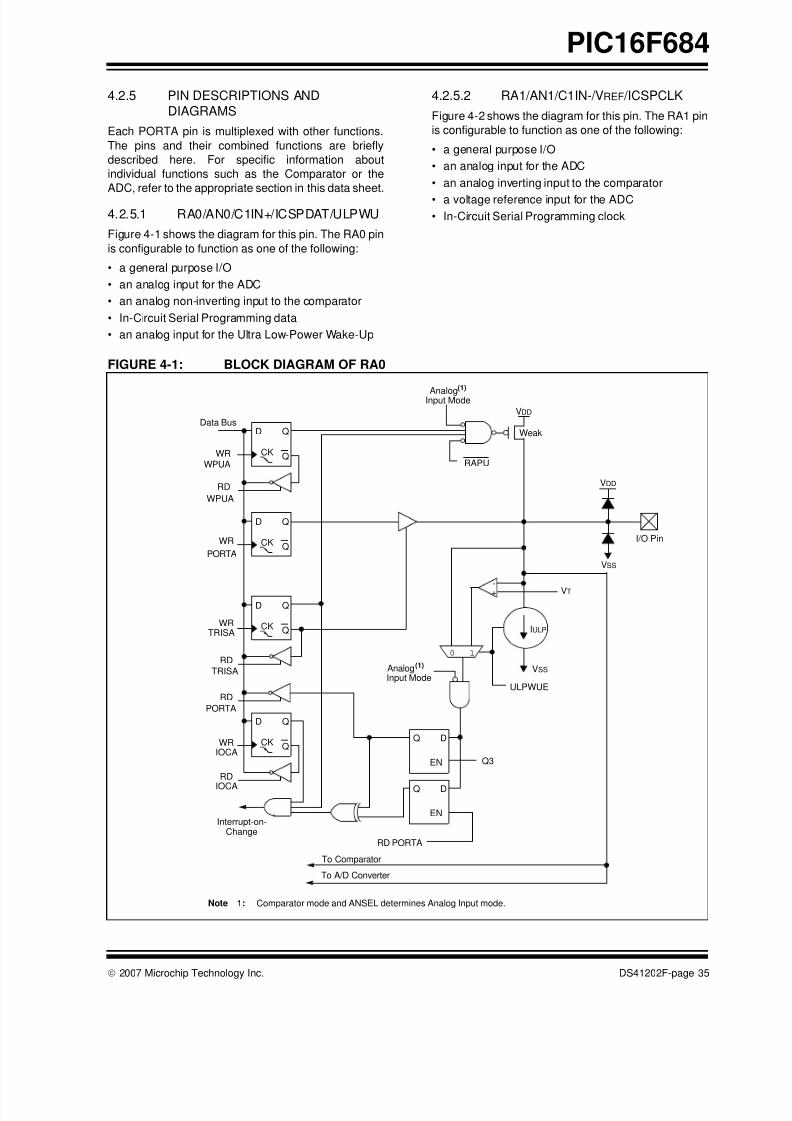
8/10/2019 PIC16F684 Datasheet
http://slidepdf.com/reader/full/pic16f684-datasheet 37/192
© 2007 Microchip Technology Inc. DS41202F-page 35
PIC16F684
4.2.5 PIN DESCRIPTIONS AND
DIAGRAMS
Each PORTA pin is multiplexed with other functions.
The pins and their combined functions are briefly
described here. For specific information about
individual functions such as the Comparator or the
ADC, refer to the appropriate section in this data sheet.
4.2.5.1 RA0/AN0/C1IN+/ICSPDAT/ULPWU
Figure 4-1 shows the diagram for this pin. The RA0 pin
is configurable to function as one of the following:
• a general purpose I/O
• an analog input for the ADC
• an analog non-inverting input to the comparator
• In-Circuit Serial Programming data
• an analog input for the Ultra Low-Power Wake-Up
4.2.5.2 RA1/AN1/C1IN-/VREF /ICSPCLK
Figure 4-2 shows the diagram for this pin. The RA1 pin
is configurable to function as one of the following:
• a general purpose I/O
• an analog input for the ADC
• an analog inverting input to the comparator
• a voltage reference input for the ADC
• In-Circuit Serial Programming clock
FIGURE 4-1: BLOCK DIAGRAM OF RA0
VDD
VSS
D
QCK
Q
D
QCK
Q
D
QCK
Q
D
QCK
Q
VDD
D
EN
Q
D
EN
Q
Weak
RD PORTA
RD
WR
WR
RD
WRIOCA
RD
IOCA
Interrupt-on-
To Comparator
Analog(1)
Input Mode
RAPU
Analog(1)
Input Mode
Change
Q3
WR
RD
0 1
IULP
WPUA
Data Bus
WPUA
PORTA
TRISA
TRISA
PORTA
Note 1: Comparator mode and ANSEL determines Analog Input mode.
-+ VT
ULPWUE
To A/D Converter
VSS
I/O Pin
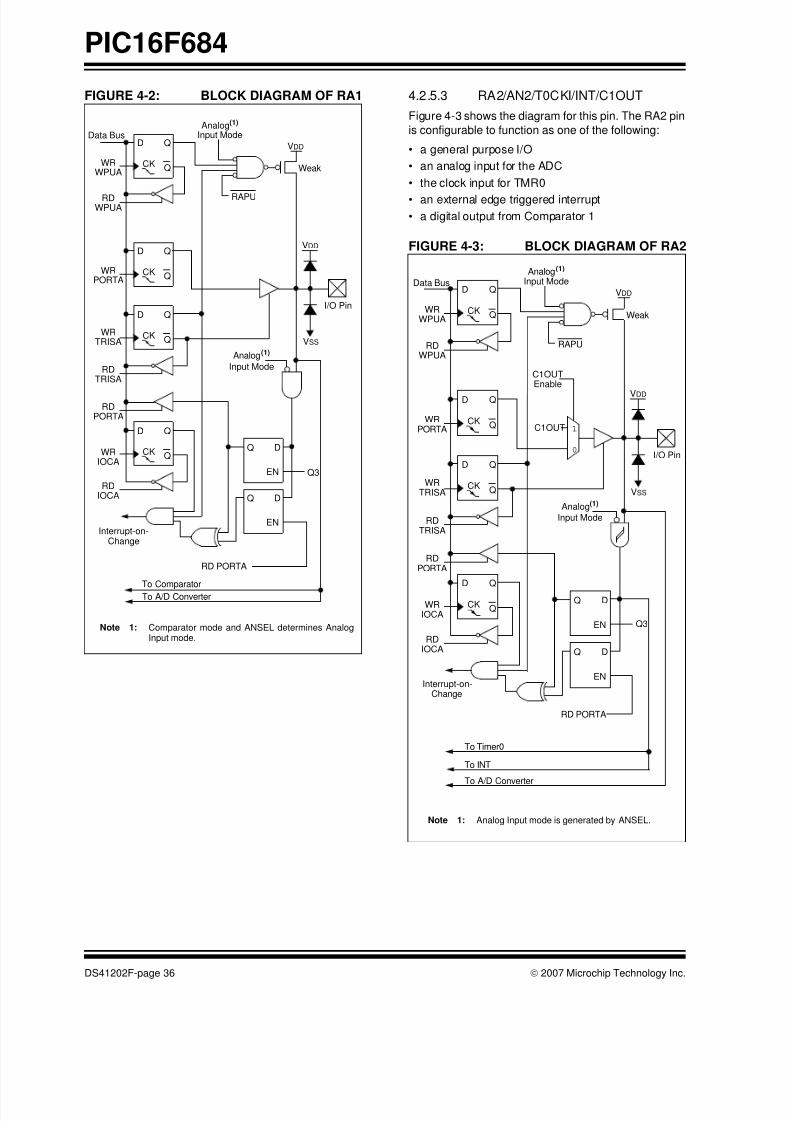
8/10/2019 PIC16F684 Datasheet
http://slidepdf.com/reader/full/pic16f684-datasheet 38/192
PIC16F684
DS41202F-page 36 © 2007 Microchip Technology Inc.
FIGURE 4-2: BLOCK DIAGRAM OF RA1 4.2.5.3 RA2/AN2/T0CKI/INT/C1OUT
Figure 4-3 shows the diagram for this pin. The RA2 pin
is configurable to function as one of the following:
• a general purpose I/O
• an analog input for the ADC
• the clock input for TMR0
• an external edge triggered interrupt
• a digital output from Comparator 1
FIGURE 4-3: BLOCK DIAGRAM OF RA2VDD
VSS
D
QCK
Q
D
QCK
Q
D
QCK
Q
D
QCK
Q
VDD
D
EN
Q
D
EN
Q
Weak
Data Bus
WRWPUA
RDWPUA
RD PORTA
RDPORTA
WRPORTA
WRTRISA
RDTRISA
WRIOCA
RDIOCA
Interrupt-on-
To Comparator
Analog(1)
Input Mode
RAPU
Analog(1)
Input Mode
Change
Q3
Note 1: Comparator mode and ANSEL determines AnalogInput mode.
To A/D Converter
I/O Pin
VDD
VSS
D
QCK
Q
D
QCK
Q
D
QCK
Q
D
QCK
Q
VDD
D
EN
Q
D
EN
Q
Weak
Analog(1)
Input Mode
Data Bus
WRWPUA
RDWPUA
RDPORTA
WRPORTA
WRTRISA
RDTRISA
WRIOCA
RDIOCA
To A/D Converter
0
1C1OUT
C1OUTEnable
To INT
To Timer0
Analog(1)
Input Mode
RAPU
RD PORTA
Interrupt-on-Change
Q3
Note 1: Analog Input mode is generated by ANSEL.
I/O Pin

8/10/2019 PIC16F684 Datasheet
http://slidepdf.com/reader/full/pic16f684-datasheet 39/192
© 2007 Microchip Technology Inc. DS41202F-page 37
PIC16F684
4.2.5.4 RA3/MCLR/VPP
Figure 4-4 shows the diagram for this pin. The RA3 pin
is configurable to function as one of the following:
• a general purpose input
• as Master Clear Reset with weak pull-up
FIGURE 4-4: BLOCK DIAGRAM OF RA3
4.2.5.5 RA4/AN3/T1G/OSC2/CLKOUT
Figure 4-5 shows the diagram for this pin. The RA4 pin
is configurable to function as one of the following:
• a general purpose I/O
• an analog input for the ADC
• a Timer1 gate (count enable)
• a crystal/resonator connection
• a clock output
FIGURE 4-5: BLOCK DIAGRAM OF RA4
VSS
D
Q
CK
Q
D
EN
Q
Data Bus
RD PORTA
RDPORTA
WR
IOCA
RDIOCA
ResetMCLRE
RDTRISA
VSS
D
EN
Q
MCLRE
VDD
WeakMCLRE
Interrupt-on-Change
Q3
InputPin
VDD
VSS
D
QCK
Q
D
QCK
Q
D
QCK
Q
D
QCK
Q
VDD
D
EN
Q
D
EN
Q
Weak
AnalogInput Mode
Data Bus
WRWPUA
RDWPUA
RDPORTA
WRPORTA
WRTRISA
RDTRISA
WRIOCA
RDIOCA
FOSC /4
To A/D Converter
Oscillator
CircuitOSC1
CLKOUT
0
1
CLKOUTEnable
Enable
Analog(3)
Input Mode
RAPU
RD PORTATo T1G
INTOSC/ RC/EC(2)
CLK(1)
Modes
CLKOUTEnable
Note 1: CLK modes are XT, HS, LP, LPTMR1 and CLKOUTEnable.
2: With CLKOUT option.
3: Analog Input mode comes from ANSEL.
Interrupt-on-Change
Q3
I/O Pin
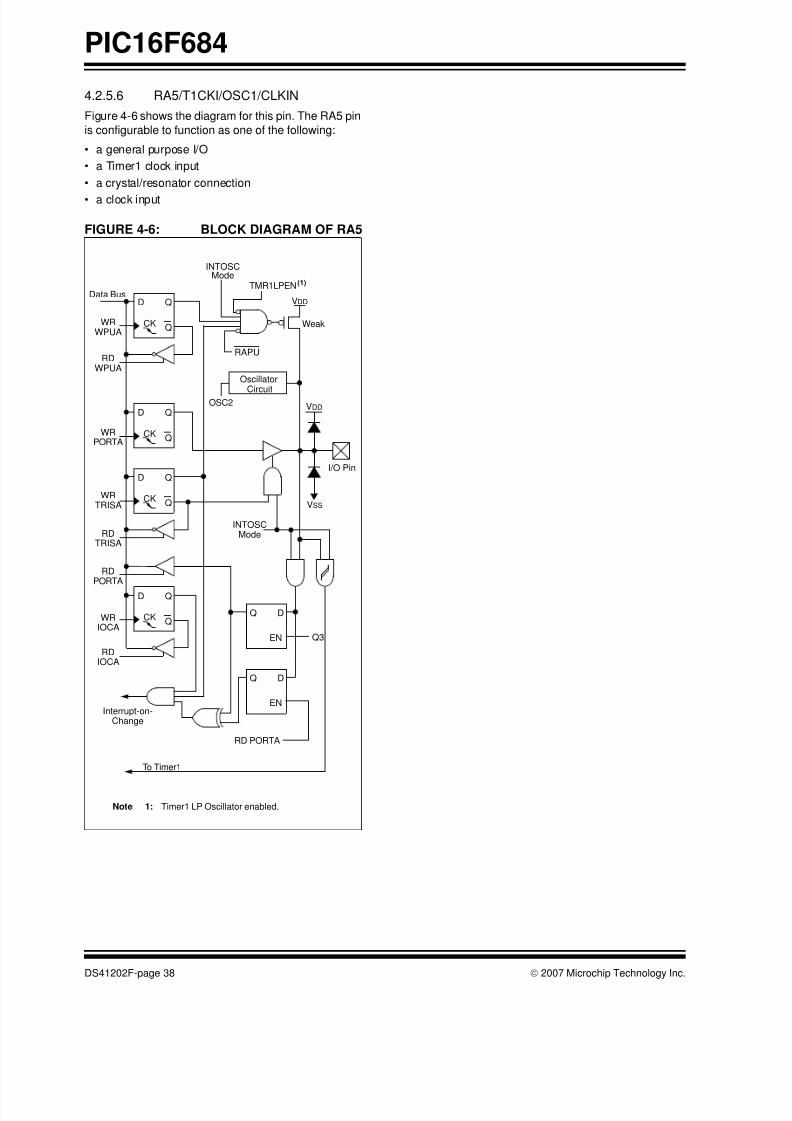
8/10/2019 PIC16F684 Datasheet
http://slidepdf.com/reader/full/pic16f684-datasheet 40/192
PIC16F684
DS41202F-page 38 © 2007 Microchip Technology Inc.
4.2.5.6 RA5/T1CKI/OSC1/CLKIN
Figure 4-6 shows the diagram for this pin. The RA5 pin
is configurable to function as one of the following:
• a general purpose I/O
• a Timer1 clock input
• a crystal/resonator connection
• a clock input
FIGURE 4-6: BLOCK DIAGRAM OF RA5
VDD
VSS
D
QCK
Q
D
QCK
Q
D
QCK
Q
D
QCK
Q
VDD
D
EN
Q
D
EN
Q
Weak
Data Bus
WRWPUA
RDWPUA
RDPORTA
WRPORTA
WRTRISA
RDTRISA
WRIOCA
RDIOCA
To Timer1
INTOSCMode
RD PORTA
INTOSCMode
RAPU
OSC2
Note 1: Timer1 LP Oscillator enabled.
TMR1LPEN(1)
Interrupt-on-Change
Oscillator
Circuit
Q3
I/O Pin

8/10/2019 PIC16F684 Datasheet
http://slidepdf.com/reader/full/pic16f684-datasheet 41/192
© 2007 Microchip Technology Inc. DS41202F-page 39
PIC16F684
TABLE 4-1: SUMMARY OF REGISTERS ASSOCIATED WITH PORTA
Name Bit 7 Bit 6 Bit 5 Bit 4 Bit 3 Bit 2 Bit 1 Bit 0Value on:
POR, BOR
Value on
all other
Resets
ANSEL ANS7 ANS6 ANS5 ANS4 ANS3 ANS2 ANS1 ANS0 1111 1111 1111 1111
CMCON0 C2OUT C1OUT C2INV C1INV CIS CM2 CM1 CM0 0000 0000 0000 0000
PCON — — ULPWUE SBOREN — — POR BOR --01 --qq --0u --uu
INTCON GIE PEIE T0IE INTE RAIE T0IF INTF RAIF 0000 0000 0000 0000
IOCA — — IOCA5 IOCA4 IOCA3 IOCA2 IOCA1 IOCA0 --00 0000 --00 0000
OPTION_REG RAPU INTEDG T0CS T0SE PSA PS2 PS1 PS0 1111 1111 1111 1111
PORTA — — RA5 RA4 RA3 RA2 RA1 RA0 --x0 x000 --uu uu00
TRISA — — TRISA5 TRISA4 TRISA3 TRISA2 TRISA1 TRISA0 --11 1111 --11 1111
WPUA — — WPUA5 WPUA4 — WPUA2 WPUA1 WPUA0 --11 -111 --11 -111
Legend: x = unknown, u = unchanged, – = unimplemented locations read as ‘0’. Shaded cells are not used by PORTA.
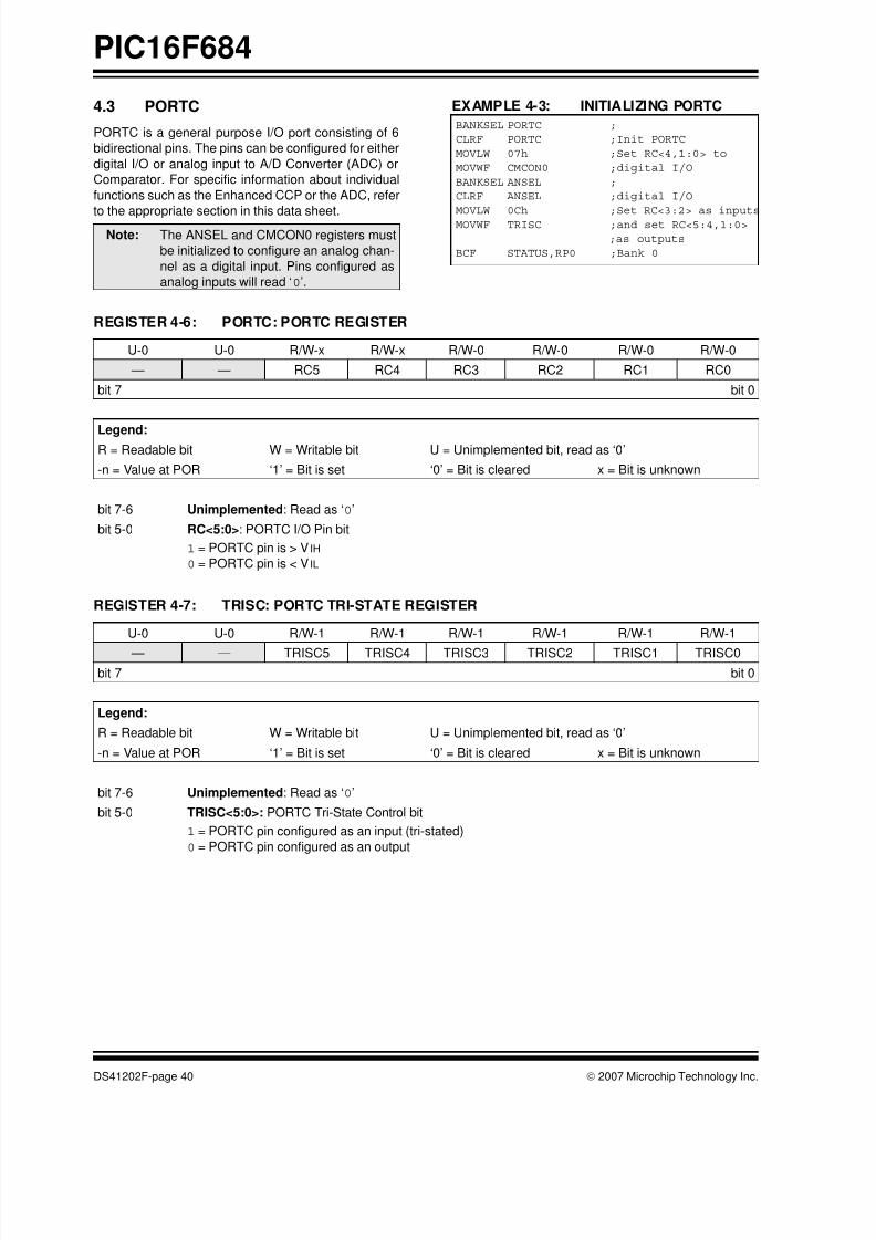
8/10/2019 PIC16F684 Datasheet
http://slidepdf.com/reader/full/pic16f684-datasheet 42/192
PIC16F684
DS41202F-page 40 © 2007 Microchip Technology Inc.
4.3 PORTC
PORTC is a general purpose I/O port consisting of 6
bidirectional pins. The pins can be configured for either
digital I/O or analog input to A/D Converter (ADC) or
Comparator. For specific information about individual
functions such as the Enhanced CCP or the ADC, refer
to the appropriate section in this data sheet.
EXAMPLE 4-3: INITIALIZING PORTC
Note: The ANSEL and CMCON0 registers must
be initialized to configure an analog chan-
nel as a digital input. Pins configured as
analog inputs will read ‘0’.
BANKSEL PORTC ;
CLRF PORTC ;Init PORTC
MOVLW 07h ;Set RC<4,1:0> to
MOVWF CMCON0 ;digital I/O
BANKSEL ANSEL ;
CLRF ANSEL ;digital I/O
MOVLW 0Ch ;Set RC<3:2> as inputs
MOVWF TRISC ;and set RC<5:4,1:0>
;as outputs
BCF STATUS,RP0 ;Bank 0
REGISTER 4-6: PORTC: PORTC REGISTER
U-0 U-0 R/W-x R/W-x R/W-0 R/W-0 R/W-0 R/W-0
— — RC5 RC4 RC3 RC2 RC1 RC0
bit 7 bit 0
Legend:R = Readable bit W = Writable bit U = Unimplemented bit, read as ‘0’
-n = Value at POR ‘1’ = Bit is set ‘0’ = Bit is cleared x = Bit is unknown
bit 7-6 Unimplemented: Read as ‘0’
bit 5-0 RC<5:0>: PORTC I/O Pin bit
1 = PORTC pin is > VIH
0 = PORTC pin is < VIL
REGISTER 4-7: TRISC: PORTC TRI-STATE REGISTER
U-0 U-0 R/W-1 R/W-1 R/W-1 R/W-1 R/W-1 R/W-1
— — TRISC5 TRISC4 TRISC3 TRISC2 TRISC1 TRISC0
bit 7 bit 0
Legend:
R = Readable bit W = Writable bit U = Unimplemented bit, read as ‘0’
-n = Value at POR ‘1’ = Bit is set ‘0’ = Bit is cleared x = Bit is unknown
bit 7-6 Unimplemented: Read as ‘0’
bit 5-0 TRISC<5:0>: PORTC Tri-State Control bit
1 = PORTC pin configured as an input (tri-stated)
0 = PORTC pin configured as an output
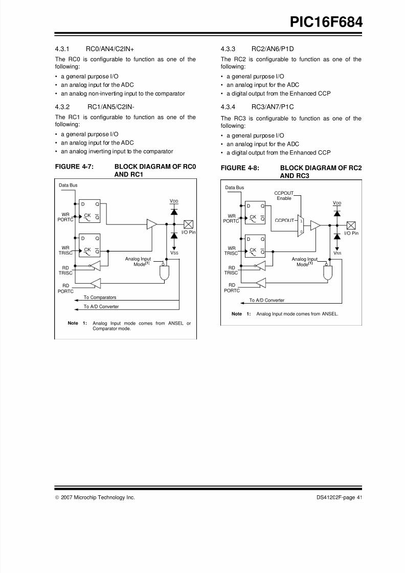
8/10/2019 PIC16F684 Datasheet
http://slidepdf.com/reader/full/pic16f684-datasheet 43/192
© 2007 Microchip Technology Inc. DS41202F-page 41
PIC16F684
4.3.1 RC0/AN4/C2IN+
The RC0 is configurable to function as one of the
following:
• a general purpose I/O
• an analog input for the ADC
• an analog non-inverting input to the comparator
4.3.2 RC1/AN5/C2IN-
The RC1 is configurable to function as one of the
following:
• a general purpose I/O
• an analog input for the ADC
• an analog inverting input to the comparator
FIGURE 4-7: BLOCK DIAGRAM OF RC0AND RC1
4.3.3 RC2/AN6/P1D
The RC2 is configurable to function as one of the
following:
• a general purpose I/O
• an analog input for the ADC
• a digital output from the Enhanced CCP
4.3.4 RC3/AN7/P1C
The RC3 is configurable to function as one of the
following:
• a general purpose I/O
• an analog input for the ADC
• a digital output from the Enhanced CCP
FIGURE 4-8: BLOCK DIAGRAM OF RC2AND RC3
I/O Pin
VDD
VSS
D
QCK
Q
D
QCK
Q
Data Bus
WRPORTC
WRTRISC
RDTRISC
To A/D Converter
RD
PORTC
Analog InputMode(1)
To Comparators
Note 1: Analog Input mode comes from ANSEL orComparator mode.
I/O Pin
VDD
VSS
D
QCK
Q
D
QCK
Q
Data Bus
WRPORTC
WRTRISC
RDTRISC
To A/D Converter
RDPORTC
Analog InputMode(1)
0
1CCPOUT
CCPOUT
Enable
Note 1: Analog Input mode comes from ANSEL.
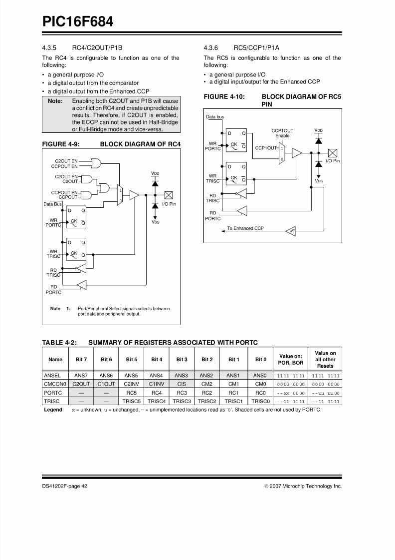
8/10/2019 PIC16F684 Datasheet
http://slidepdf.com/reader/full/pic16f684-datasheet 44/192
PIC16F684
DS41202F-page 42 © 2007 Microchip Technology Inc.
4.3.5 RC4/C2OUT/P1B
The RC4 is configurable to function as one of the
following:
• a general purpose I/O
• a digital output from the comparator
• a digital output from the Enhanced CCP
FIGURE 4-9: BLOCK DIAGRAM OF RC4
4.3.6 RC5/CCP1/P1A
The RC5 is configurable to function as one of the
following:
• a general purpose I/O
• a digital input/output for the Enhanced CCP
FIGURE 4-10: BLOCK DIAGRAM OF RC5PIN
TABLE 4-2: SUMMARY OF REGISTERS ASSOCIATED WITH PORTC
Note: Enabling both C2OUT and P1B will cause
a conflict on RC4 and create unpredictable
results. Therefore, if C2OUT is enabled,
the ECCP can not be used in Half-Bridge
or Full-Bridge mode and vice-versa.
I/O Pin
VDD
VSS
D
QCK
Q
D
QCK
Q
Data Bus
WRPORTC
WRTRISC
RDTRISC
RD
PORTC
0
1
Note 1: Port/Peripheral Select signals selects betweenport data and peripheral output.
C2OUT ENCCPOUT EN
C2OUT ENC2OUT
CCPOUT ENCCPOUT
I/O Pin
VDD
VSS
D
QCK
Q
D
QCK
Q
Data bus
WRPORTC
WRTRISC
RDTRISC
To Enhanced CCP
RD
PORTC
0
1CCP1OUT
CCP1OUTEnable
Name Bit 7 Bit 6 Bit 5 Bit 4 Bit 3 Bit 2 Bit 1 Bit 0Value on:
POR, BOR
Value on
all other
Resets
ANSEL ANS7 ANS6 ANS5 ANS4 ANS3 ANS2 ANS1 ANS0 1111 1111 1111 1111
CMCON0 C2OUT C1OUT C2INV C1INV CIS CM2 CM1 CM0 0000 0000 0000 0000
PORTC — — RC5 RC4 RC3 RC2 RC1 RC0 --xx 0000 --uu uu00
TRISC — — TRISC5 TRISC4 TRISC3 TRISC2 TRISC1 TRISC0 --11 1111 --11 1111
Legend: x = unknown, u = unchanged, – = unimplemented locations read as ‘0’. Shaded cells are not used by PORTC.

8/10/2019 PIC16F684 Datasheet
http://slidepdf.com/reader/full/pic16f684-datasheet 45/192
© 2007 Microchip Technology Inc. DS41202F-page 43
PIC16F684
5.0 TIMER0 MODULE
The Timer0 module is an 8-bit timer/counter with the
following features:
• 8-bit timer/counter register (TMR0)
• 8-bit prescaler (shared with Watchdog Timer)
• Programmable internal or external clock source
• Programmable external clock edge selection
• Interrupt on overflow
Figure 5-1 is a block diagram of the Timer0 module.
5.1 Timer0 Operation
When used as a timer, the Timer0 module can be used
as either an 8-bit timer or an 8-bit counter.
5.1.1 8-BIT TIMER MODE
When used as a timer, the Timer0 module will
increment every instruction cycle (without prescaler).Timer mode is selected by clearing the T0CS bit of the
OPTION register to ‘0’.
When TMR0 is written, the increment is inhibited for
two instruction cycles immediately following the write.
5.1.2 8-BIT COUNTER MODE
When used as a counter, the Timer0 module will
increment on every rising or falling edge of the T0CKI
pin. The incrementing edge is determined by the T0SEbit of the OPTION register. Counter mode is selected by
setting the T0CS bit of the OPTION register to ‘1’.
FIGURE 5-1: BLOCK DIAGRAM OF THE TIMER0/WDT PRESCALER
Note: The value written to the TMR0 register can
be adjusted, in order to account for the two
instruction cycle delay when TMR0 is
written.
T0CKI
T0SE
pin
TMR0
WatchdogTimer
WDTTime-out
PS<2:0>
WDTE
Data Bus
Set Flag bit T0IFon Overflow
T0CS
Note 1: T0SE, T0CS, PSA, PS<2:0> are bits in the OPTION register.
2: SWDTEN and WDTPS<3:0> are bits in the WDTCON register.
3: WDTE bit is in the Configuration Word register.
0
1
0
1
0
1
Sync 2cycles
8
8
8-bitPrescaler
0
1
FOSC /4
PSA
PSA
PSA
16-bitPrescaler
16
WDTPS<3:0>
31 kHzINTOSC
SWDTEN3
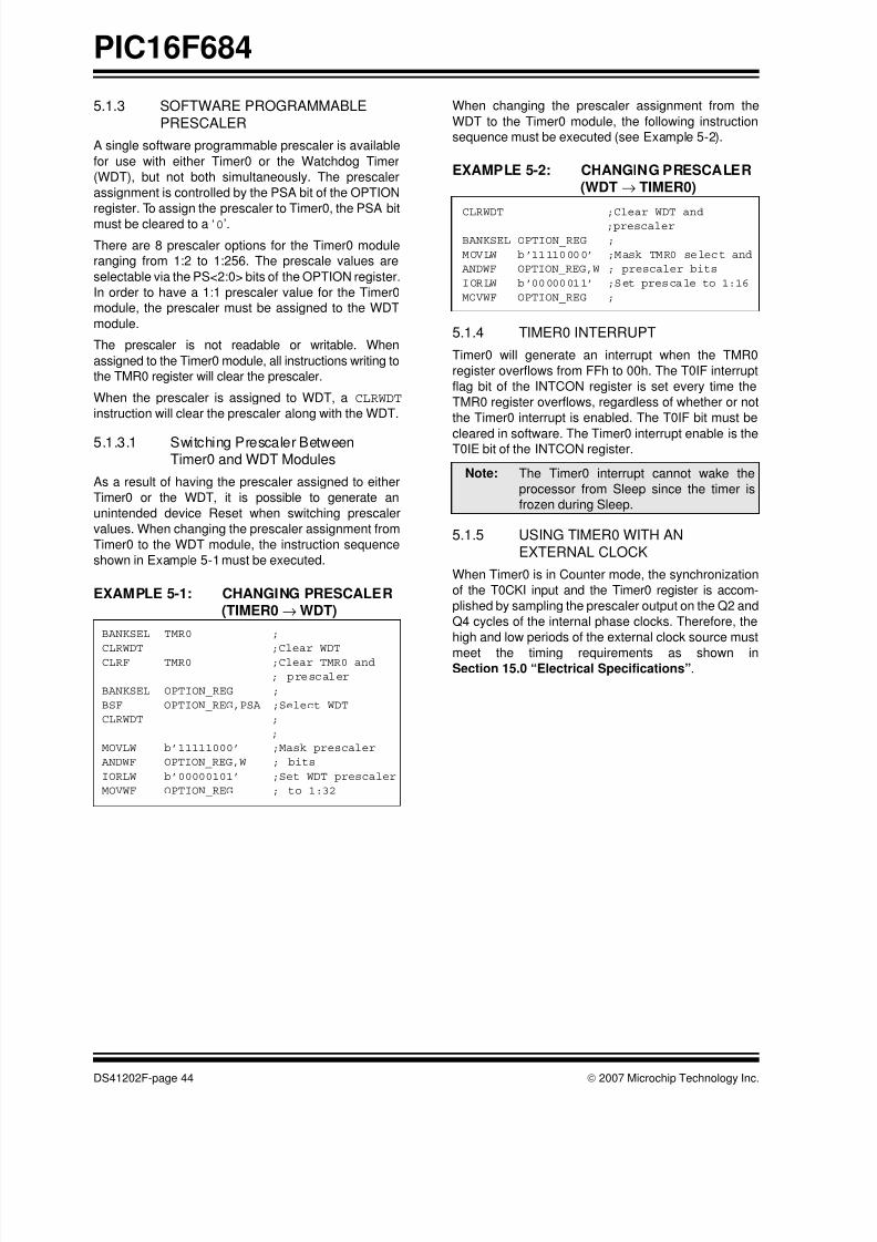
8/10/2019 PIC16F684 Datasheet
http://slidepdf.com/reader/full/pic16f684-datasheet 46/192
PIC16F684
DS41202F-page 44 © 2007 Microchip Technology Inc.
5.1.3 SOFTWARE PROGRAMMABLE
PRESCALER
A single software programmable prescaler is available
for use with either Timer0 or the Watchdog Timer
(WDT), but not both simultaneously. The prescaler
assignment is controlled by the PSA bit of the OPTION
register. To assign the prescaler to Timer0, the PSA bit
must be cleared to a ‘0’.
There are 8 prescaler options for the Timer0 module
ranging from 1:2 to 1:256. The prescale values are
selectable via the PS<2:0> bits of the OPTION register.
In order to have a 1:1 prescaler value for the Timer0
module, the prescaler must be assigned to the WDT
module.
The prescaler is not readable or writable. When
assigned to the Timer0 module, all instructions writing to
the TMR0 register will clear the prescaler.
When the prescaler is assigned to WDT, a CLRWDT
instruction will clear the prescaler along with the WDT.
5.1.3.1 Switching Prescaler BetweenTimer0 and WDT Modules
As a result of having the prescaler assigned to either
Timer0 or the WDT, it is possible to generate an
unintended device Reset when switching prescaler
values. When changing the prescaler assignment from
Timer0 to the WDT module, the instruction sequence
shown in Example 5-1 must be executed.
EXAMPLE 5-1: CHANGING PRESCALER(TIMER0 → WDT)
When changing the prescaler assignment from the
WDT to the Timer0 module, the following instruction
sequence must be executed (see Example 5-2).
EXAMPLE 5-2: CHANGING PRESCALER(WDT → TIMER0)
5.1.4 TIMER0 INTERRUPT
Timer0 will generate an interrupt when the TMR0
register overflows from FFh to 00h. The T0IF interrupt
flag bit of the INTCON register is set every time the
TMR0 register overflows, regardless of whether or not
the Timer0 interrupt is enabled. The T0IF bit must be
cleared in software. The Timer0 interrupt enable is theT0IE bit of the INTCON register.
5.1.5 USING TIMER0 WITH AN
EXTERNAL CLOCK
When Timer0 is in Counter mode, the synchronization
of the T0CKI input and the Timer0 register is accom-
plished by sampling the prescaler output on the Q2 and
Q4 cycles of the internal phase clocks. Therefore, the
high and low periods of the external clock source must
meet the timing requirements as shown inSection 15.0 “Electrical Specifications”.
BANKSEL TMR0 ;
CLRWDT ;Clear WDTCLRF TMR0 ;Clear TMR0 and
; prescaler
BANKSEL OPTION_REG ;
BSF OPTION_REG,PSA ;Select WDT
CLRWDT ;
;
MOVLW b’11111000’ ;Mask prescaler
ANDWF OPTION_REG,W ; bits
IORLW b’00000101’ ;Set WDT prescaler
MOVWF OPTION_REG ; to 1:32
Note: The Timer0 interrupt cannot wake the
processor from Sleep since the timer is
frozen during Sleep.
CLRWDT ;Clear WDT and;prescaler
BANKSEL OPTION_REG ;
MOVLW b’11110000’ ;Mask TMR0 select and
ANDWF OPTION_REG,W ; prescaler bits
IORLW b’00000011’ ;Set prescale to 1:16
MOVWF OPTION_REG ;

8/10/2019 PIC16F684 Datasheet
http://slidepdf.com/reader/full/pic16f684-datasheet 47/192
© 2007 Microchip Technology Inc. DS41202F-page 45
PIC16F684
TABLE 5-1: SUMMARY OF REGISTERS ASSOCIATED WITH TIMER0
REGISTER 5-1: OPTION_REG: OPTION REGISTER
R/W-1 R/W-1 R/W-1 R/W-1 R/W-1 R/W-1 R/W-1 R/W-1
RAPU INTEDG T0CS T0SE PSA PS2 PS1 PS0
bit 7 bit 0
Legend:
R = Readable bit W = Writable bit U = Unimplemented bit, read as ‘0’
-n = Value at POR ‘1’ = Bit is set ‘0’ = Bit is cleared x = Bit is unknown
bit 7 RAPU: PORTA Pull-up Enable bit
1 = PORTA pull-ups are disabled
0 = PORTA pull-ups are enabled by individual PORT latch values
bit 6 INTEDG: Interrupt Edge Select bit
1 = Interrupt on rising edge of INT pin
0 = Interrupt on falling edge of INT pin
bit 5 T0CS: TMR0 Clock Source Select bit
1 = Transition on T0CKI pin0 = Internal instruction cycle clock (FOSC /4)
bit 4 T0SE: TMR0 Source Edge Select bit
1 = Increment on high-to-low transition on T0CKI pin
0 = Increment on low-to-high transition on T0CKI pin
bit 3 PSA: Prescaler Assignment bit
1 = Prescaler is assigned to the WDT
0 = Prescaler is assigned to the Timer0 module
bit 2-0 PS<2:0>: Prescaler Rate Select bits
Note 1: A dedicated 16-bit WDT postscaler is available. See Section 12.6 “Watchdog Timer (WDT)” for more
information.
000
001
010
011
100
101
110
111
1 : 2
1 : 4
1 : 8
1 : 16
1 : 32
1 : 64
1 : 128
1 : 256
1 : 1
1 : 2
1 : 4
1 : 8
1 : 16
1 : 32
1 : 64
1 : 128
BIT VALUE TMR0 RATE WDT RATE
Name Bit 7 Bit 6 Bit 5 Bit 4 Bit 3 Bit 2 Bit 1 Bit 0 Value on:POR, BOR
Value on
all otherResets
TMR0 Timer0 Module Register xxxx xxxx uuuu uuuu
INTCON GIE PEIE T0IE INTE RAIE T0IF INTF RAIF 0000 0000 0000 0000
OPTION_REG RAPU INTEDG T0CS T0SE PSA PS2 PS1 PS0 1111 1111 1111 1111
TRISA — — TRISA5 TRISA4 TRISA3 TRISA2 TRISA1 TRISA0 --11 1111 --11 1111
Legend: – = Unimplemented locations, read as ‘0’, u = unchanged, x = unknown. Shaded cells are not used by the
Timer0 module.

8/10/2019 PIC16F684 Datasheet
http://slidepdf.com/reader/full/pic16f684-datasheet 48/192
PIC16F684
DS41202F-page 46 © 2007 Microchip Technology Inc.
NOTES:

8/10/2019 PIC16F684 Datasheet
http://slidepdf.com/reader/full/pic16f684-datasheet 49/192
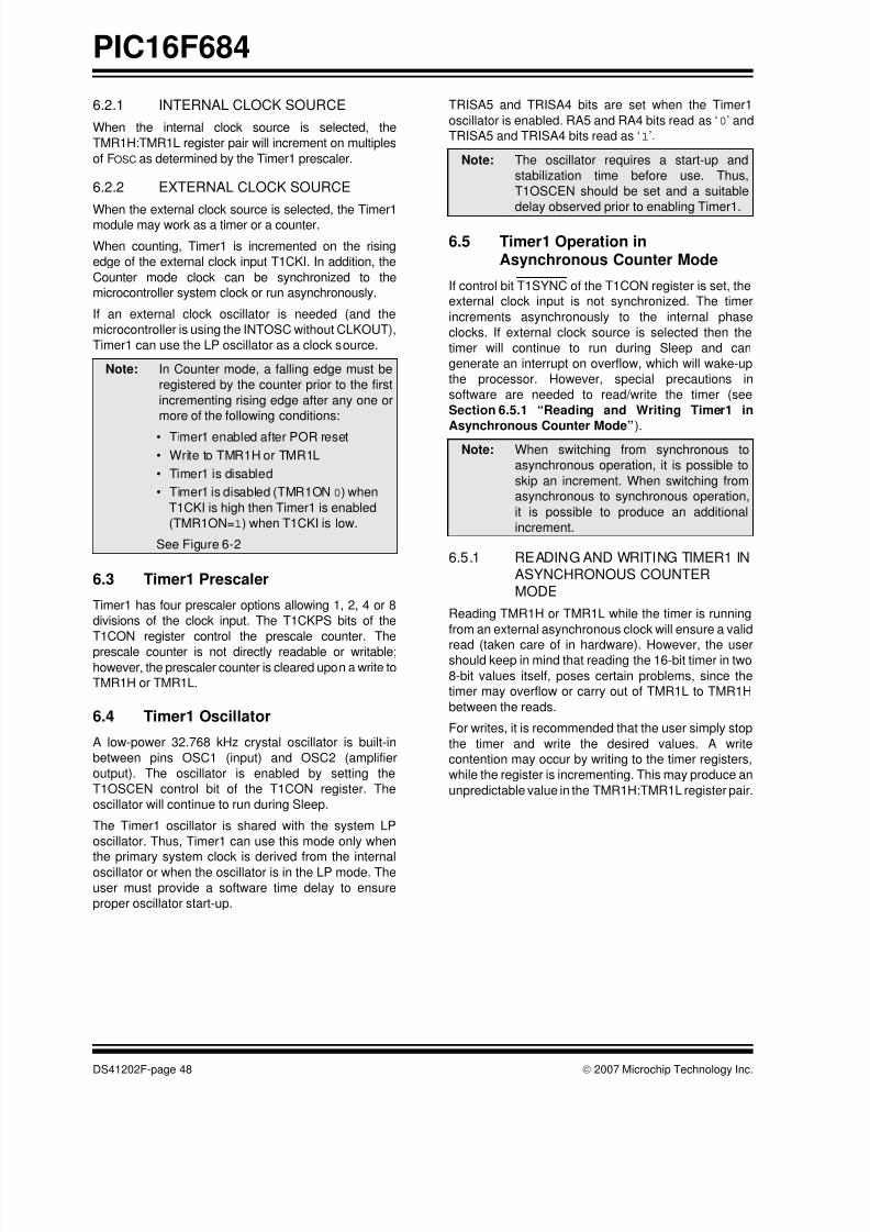
8/10/2019 PIC16F684 Datasheet
http://slidepdf.com/reader/full/pic16f684-datasheet 50/192
PIC16F684
DS41202F-page 48 © 2007 Microchip Technology Inc.
6.2.1 INTERNAL CLOCK SOURCE
When the internal clock source is selected, the
TMR1H:TMR1L register pair will increment on multiples
of FOSC as determined by the Timer1 prescaler.
6.2.2 EXTERNAL CLOCK SOURCE
When the external clock source is selected, the Timer1module may work as a timer or a counter.
When counting, Timer1 is incremented on the rising
edge of the external clock input T1CKI. In addition, the
Counter mode clock can be synchronized to the
microcontroller system clock or run asynchronously.
If an external clock oscillator is needed (and the
microcontroller is using the INTOSC without CLKOUT),
Timer1 can use the LP oscillator as a clock source.
6.3 Timer1 Prescaler
Timer1 has four prescaler options allowing 1, 2, 4 or 8
divisions of the clock input. The T1CKPS bits of the
T1CON register control the prescale counter. The
prescale counter is not directly readable or writable;however, the prescaler counter is cleared upon a write to
TMR1H or TMR1L.
6.4 Timer1 Oscillator
A low-power 32.768 kHz crystal oscillator is built-in
between pins OSC1 (input) and OSC2 (amplifier
output). The oscillator is enabled by setting the
T1OSCEN control bit of the T1CON register. The
oscillator will continue to run during Sleep.
The Timer1 oscillator is shared with the system LP
oscillator. Thus, Timer1 can use this mode only when
the primary system clock is derived from the internal
oscillator or when the oscillator is in the LP mode. The
user must provide a software time delay to ensure
proper oscillator start-up.
TRISA5 and TRISA4 bits are set when the Timer1
oscillator is enabled. RA5 and RA4 bits read as ‘0’ and
TRISA5 and TRISA4 bits read as ‘1’.
6.5 Timer1 Operation inAsynchronous Counter Mode
If control bit T1SYNC of the T1CON register is set, the
external clock input is not synchronized. The timer
increments asynchronously to the internal phase
clocks. If external clock source is selected then the
timer will continue to run during Sleep and can
generate an interrupt on overflow, which will wake-up
the processor. However, special precautions in
software are needed to read/write the timer (see
Section 6.5.1 “Reading and Writing Timer1 in
Asynchronous Counter Mode”).
6.5.1 READING AND WRITING TIMER1 INASYNCHRONOUS COUNTER
MODE
Reading TMR1H or TMR1L while the timer is running
from an external asynchronous clock will ensure a valid
read (taken care of in hardware). However, the usershould keep in mind that reading the 16-bit timer in two
8-bit values itself, poses certain problems, since the
timer may overflow or carry out of TMR1L to TMR1H
between the reads.
For writes, it is recommended that the user simply stop
the timer and write the desired values. A write
contention may occur by writing to the timer registers,
while the register is incrementing. This may produce an
unpredictable value in the TMR1H:TMR1L register pair.
Note: In Counter mode, a falling edge must be
registered by the counter prior to the first
incrementing rising edge after any one or
more of the following conditions:
• Timer1 enabled after POR reset
• Write to TMR1H or TMR1L
• Timer1 is disabled
• Timer1 is disabled (TMR1ON 0) when
T1CKI is high then Timer1 is enabled
(TMR1ON=1) when T1CKI is low.
See Figure 6-2
Note: The oscillator requires a start-up and
stabilization time before use. Thus,
T1OSCEN should be set and a suitable
delay observed prior to enabling Timer1.
Note: When switching from synchronous to
asynchronous operation, it is possible to
skip an increment. When switching from
asynchronous to synchronous operation,
it is possible to produce an additional
increment.

8/10/2019 PIC16F684 Datasheet
http://slidepdf.com/reader/full/pic16f684-datasheet 51/192
© 2007 Microchip Technology Inc. DS41202F-page 49
PIC16F684
6.6 Timer1 Gate
Timer1 gate source is software configurable to be the
T1G pin or the output of Comparator 2. This allows the
device to directly time external events using T1G or
analog events using Comparator 2. See the CMCON1
register (Register 8-2) for selecting the Timer1 gate
source. This feature can simplify the software for aDelta-Sigma A/D converter and many other applications.
For more information on Delta-Sigma A/D converters,
see the Microchip web site (www.microchip.com).
Timer1 gate can be inverted using the T1GINV bit of
the T1CON register, whether it originates from the T1G
pin or Comparator 2 output. This configures Timer1 to
measure either the active-high or active-low time
between events.
6.7 Timer1 Interrupt
The Timer1 register pair (TMR1H:TMR1L) increments
to FFFFh and rolls over to 0000h. When Timer1 rolls
over, the Timer1 interrupt flag bit of the PIR1 register is
set. To enable the interrupt on rollover, you must set
these bits:
• TMR1ON bit or the T1CON register
• TMR1IE bit of the PIE1 register
• PEIE bit of the INTCON register
• GIE bit of the INTCON register
The interrupt is cleared by clearing the TMR1IF bit inthe Interrupt Service Routine.
6.8 Timer1 Operation During Sleep
Timer1 can only operate during Sleep when setup in
Asynchronous Counter mode. In this mode, an external
crystal or clock source can be used to increment the
counter. To set up the timer to wake the device:
• TMR1ON bit of the T1CON register must be set
• TMR1IE bit of the PIE1 register must be set• PEIE bit of the INTCON register must be set
• T1SYNC bit of the T1CON register
• TMR1CS bit of the T1CON register
• T1OSCEN bit of the T1CON register (can be set)
The device will wake-up on an overflow and execute
the next instruction. If the GIE bit of the INTCON
register is set, the device will call the Interrupt Service
Routine (0004h).
6.9 ECCP Capture/Compare Time Base
The ECCP module uses the TMR1H:TMR1L register
pair as the time base when operating in Capture or
Compare mode.
In Capture mode, the value in the TMR1H:TMR1L
register pair is copied into the CCPR1H:CCPR1L
register pair on a configured event.
In Compare mode, an event is triggered when the value
CCPR1H:CCPR1L register pair matches the value in
the TMR1H:TMR1L register pair. This event can be a
Special Event Trigger.
For more information, see Section 11.0 “Enhanced
Capture/Compare/PWM (With Auto-Shutdown and
Dead Band) Module”.
6.10 ECCP Special Event Trigger
When the ECCP is configured to trigger a special
event, the trigger will clear the TMR1H:TMR1L register
pair. This special event does not cause a Timer1interrupt. The ECCP module may still be configured to
generate a ECCP interrupt.
In this mode of operation, the CCPR1H:CCPR1L
register pair effectively becomes the period register for
Timer1.
Timer1 should be synchronized to the FOSC to utilize
the Special Event Trigger. Asynchronous operation of
Timer1 can cause a Special Event Trigger to be
missed.
In the event that a write to TMR1H or TMR1L coincides
with a Special Event Trigger from the ECCP, the write
will take precedence.
For more information, see Section 11.2.4 “SpecialEvent Trigger”.
6.11 Comparator Synchronization
The same clock used to increment Timer1 can also be
used to synchronize the comparator output. This
feature is enabled in the Comparator module.
When using the comparator for Timer1 gate, the
comparator output should be synchronized to Timer1.
This ensures Timer1 does not miss an increment if the
comparator changes.
For more information, see Section 8.9 “Synchronizing
Comparator C2 Output to Timer1”.
Note: TMR1GE bit of the T1CON register must
be set to use either T1G or C2OUT as the
Timer1 gate source. See the CMCON1
register (Register 8-2) for more informa-
tion on selecting the Timer1 gate source.
Note: The TMR1H:TTMR1L register pair and the
TMR1IF bit should be cleared before
enabling interrupts.
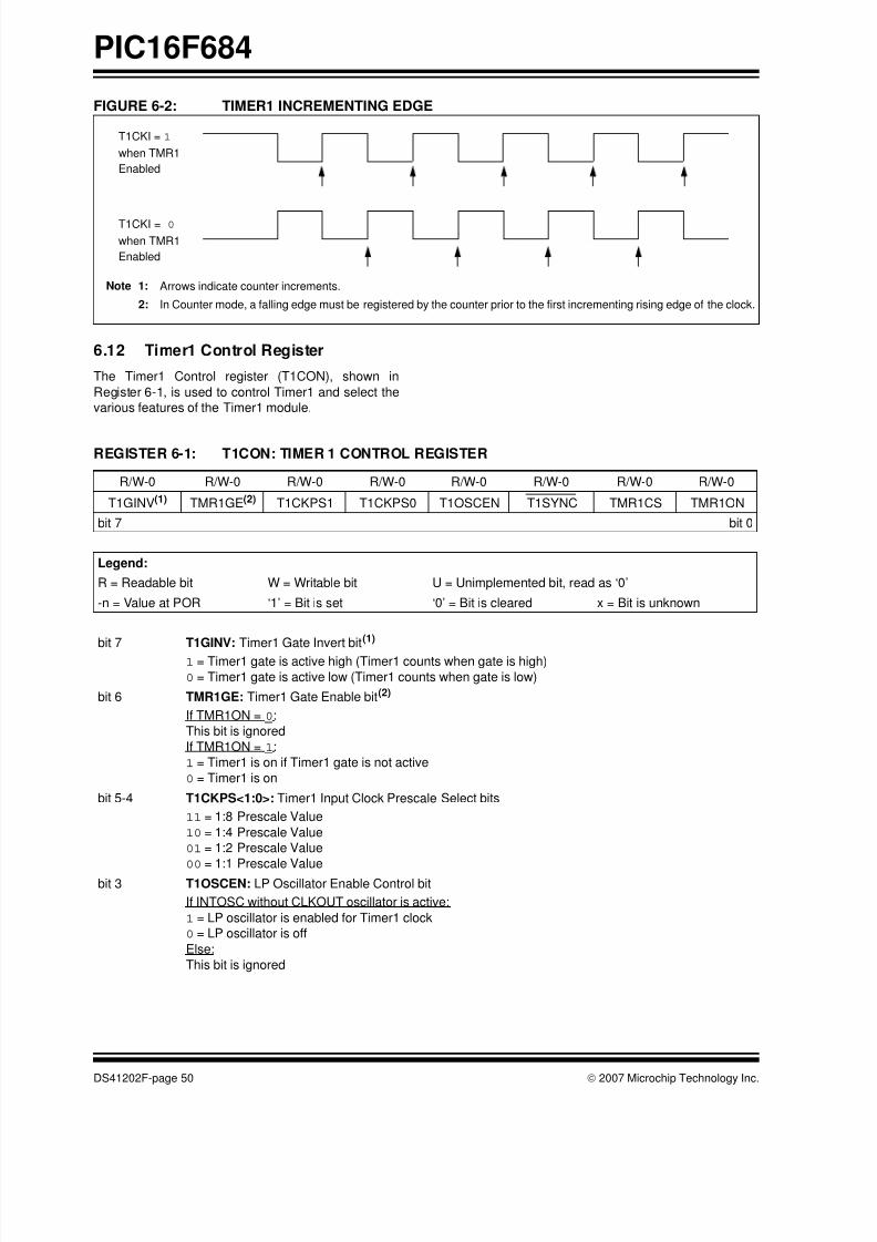
8/10/2019 PIC16F684 Datasheet
http://slidepdf.com/reader/full/pic16f684-datasheet 52/192
PIC16F684
DS41202F-page 50 © 2007 Microchip Technology Inc.
FIGURE 6-2: TIMER1 INCREMENTING EDGE
6.12 Timer1 Control Register
The Timer1 Control register (T1CON), shown in
Register 6-1, is used to control Timer1 and select the
various features of the Timer1 module.
T1CKI = 1
when TMR1
Enabled
T1CKI = 0
when TMR1
Enabled
Note 1: Arrows indicate counter increments.
2: In Counter mode, a falling edge must be registered by the counter prior to the first incrementing rising edge of the clock.
REGISTER 6-1: T1CON: TIMER 1 CONTROL REGISTER
R/W-0 R/W-0 R/W-0 R/W-0 R/W-0 R/W-0 R/W-0 R/W-0
T1GINV(1) TMR1GE(2) T1CKPS1 T1CKPS0 T1OSCEN T1SYNC TMR1CS TMR1ON
bit 7 bit 0
Legend:
R = Readable bit W = Writable bit U = Unimplemented bit, read as ‘0’
-n = Value at POR ‘1’ = Bit is set ‘0’ = Bit is cleared x = Bit is unknown
bit 7 T1GINV: Timer1 Gate Invert bit(1)
1 = Timer1 gate is active high (Timer1 counts when gate is high)
0 = Timer1 gate is active low (Timer1 counts when gate is low)
bit 6 TMR1GE: Timer1 Gate Enable bit(2)
If TMR1ON = 0:
This bit is ignored
If TMR1ON = 1:
1 = Timer1 is on if Timer1 gate is not active
0 = Timer1 is on
bit 5-4 T1CKPS<1:0>: Timer1 Input Clock Prescale Select bits
11 = 1:8 Prescale Value
10 = 1:4 Prescale Value
01 = 1:2 Prescale Value
00 = 1:1 Prescale Value
bit 3 T1OSCEN: LP Oscillator Enable Control bit
If INTOSC without CLKOUT oscillator is active:
1 = LP oscillator is enabled for Timer1 clock
0 = LP oscillator is off
Else:
This bit is ignored
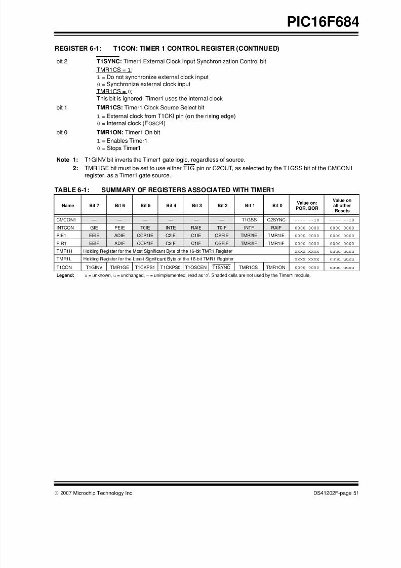
8/10/2019 PIC16F684 Datasheet
http://slidepdf.com/reader/full/pic16f684-datasheet 53/192
© 2007 Microchip Technology Inc. DS41202F-page 51
PIC16F684
TABLE 6-1: SUMMARY OF REGISTERS ASSOCIATED WITH TIMER1
bit 2 T1SYNC: Timer1 External Clock Input Synchronization Control bit
TMR1CS = 1:
1 = Do not synchronize external clock input
0 = Synchronize external clock input
TMR1CS = 0:
This bit is ignored. Timer1 uses the internal clockbit 1 TMR1CS: Timer1 Clock Source Select bit
1 = External clock from T1CKI pin (on the rising edge)
0 = Internal clock (FOSC /4)
bit 0 TMR1ON: Timer1 On bit
1 = Enables Timer1
0 = Stops Timer1
Note 1: T1GINV bit inverts the Timer1 gate logic, regardless of source.
2: TMR1GE bit must be set to use either T1G pin or C2OUT, as selected by the T1GSS bit of the CMCON1
register, as a Timer1 gate source.
Name Bit 7 Bit 6 Bit 5 Bit 4 Bit 3 Bit 2 Bit 1 Bit 0Value on:POR, BOR
Value onall otherResets
CMCON1 — — — — — — T1GSS C2SYNC ---- --10 ---- --10
INTCON GIE PEIE T0IE INTE RAIE T0IF INTF RAIF 0000 0000 0000 0000
PIE1 EEIE ADIE CCP1IE C2IE C1IE OSFIE TMR2IE TMR1IE 0000 0000 0000 0000
PIR1 EEIF ADIF CCP1IF C2IF C1IF OSFIF TMR2IF TMR1IF 0000 0000 0000 0000
TMR1H Holding Register for the Most Significant Byte of the 16-bit TMR1 Register xxxx xxxx uuuu uuuu
TMR1L Holding Register for the Least Significant Byte of the 16-bit TMR1 Register xxxx xxxx uuuu uuuu
T1CON T1GINV TMR1GE T1CKPS1 T1CKPS0 T1OSCEN T1SYNC TMR1CS TMR1ON 0000 0000 uuuu uuuu
Legend: x = unknown, u = unchanged, — = unimplemented, read as ‘0’. Shaded cells are not used by the Timer1 module.
REGISTER 6-1: T1CON: TIMER 1 CONTROL REGISTER (CONTINUED)

8/10/2019 PIC16F684 Datasheet
http://slidepdf.com/reader/full/pic16f684-datasheet 54/192
PIC16F684
DS41202F-page 52 © 2007 Microchip Technology Inc.
NOTES:

8/10/2019 PIC16F684 Datasheet
http://slidepdf.com/reader/full/pic16f684-datasheet 55/192
© 2007 Microchip Technology Inc. DS41202F-page 53
PIC16F684
7.0 TIMER2 MODULE
The Timer2 module is an eight-bit timer with the
following features:
• 8-bit timer register (TMR2)
• 8-bit period register (PR2)
• Interrupt on TMR2 match with PR2
• Software programmable prescaler (1:1, 1:4, 1:16)
• Software programmable postscaler (1:1 to 1:16)
See Figure 7-1 for a block diagram of Timer2.
7.1 Timer2 Operation
The clock input to the Timer2 module is the system
instruction clock (FOSC /4). The clock is fed into the
Timer2 prescaler, which has prescale options of 1:1,
1:4 or 1:16. The output of the prescaler is then used to
increment the TMR2 register.
The values of TMR2 and PR2 are constantly compared
to determine when they match. TMR2 will increment
from 00h until it matches the value in PR2. When a
match occurs, two things happen:
• TMR2 is reset to 00h on the next increment cycle.
• The Timer2 postscaler is incremented
The match output of the Timer2/PR2 comparator is fed
into the Timer2 postscaler. The postscaler has
postscale options of 1:1 to 1:16 inclusive. The output of
the Timer2 postscaler is used to set the TMR2IF
interrupt flag bit in the PIR1 register.
The TMR2 and PR2 registers are both fully readable
and writable. On any Reset, the TMR2 register is set to
00h and the PR2 register is set to FFh.
Timer2 is turned on by setting the TMR2ON bit in the
T2CON register to a ‘1’. Timer2 is turned off by clearing
the TMR2ON bit to a ‘0’.
The Timer2 prescaler is controlled by the T2CKPS bitsin the T2CON register. The Timer2 postscaler is
controlled by the TOUTPS bits in the T2CON register.
The prescaler and postscaler counters are cleared
when:
• A write to TMR2 occurs.
• A write to T2CON occurs.
• Any device Reset occurs (Power-on Reset, MCLR
Reset, Watchdog Timer Reset, or Brown-out
Reset).
FIGURE 7-1: TIMER2 BLOCK DIAGRAM
Note: TMR2 is not cleared when T2CON is
written.
Comparator
TMR2Sets Flag
TMR2
Output
Reset
Postscaler
Prescaler
PR2
2
FOSC /4
1:1 to 1:16
1:1, 1:4, 1:16
EQ
4
bit TMR2IF
TOUTPS<3:0>
T2CKPS<1:0>
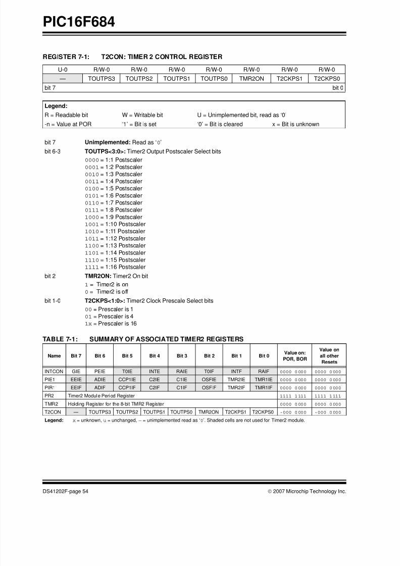
8/10/2019 PIC16F684 Datasheet
http://slidepdf.com/reader/full/pic16f684-datasheet 56/192
PIC16F684
DS41202F-page 54 © 2007 Microchip Technology Inc.
TABLE 7-1: SUMMARY OF ASSOCIATED TIMER2 REGISTERS
REGISTER 7-1: T2CON: TIMER 2 CONTROL REGISTER
U-0 R/W-0 R/W-0 R/W-0 R/W-0 R/W-0 R/W-0 R/W-0
— TOUTPS3 TOUTPS2 TOUTPS1 TOUTPS0 TMR2ON T2CKPS1 T2CKPS0
bit 7 bit 0
Legend:
R = Readable bit W = Writable bit U = Unimplemented bit, read as ‘0’
-n = Value at POR ‘1’ = Bit is set ‘0’ = Bit is cleared x = Bit is unknown
bit 7 Unimplemented: Read as ‘0’
bit 6-3 TOUTPS<3:0>: Timer2 Output Postscaler Select bits
0000 = 1:1 Postscaler
0001 = 1:2 Postscaler
0010 = 1:3 Postscaler
0011 = 1:4 Postscaler
0100 = 1:5 Postscaler
0101 = 1:6 Postscaler0110 = 1:7 Postscaler
0111 = 1:8 Postscaler
1000 = 1:9 Postscaler
1001 = 1:10 Postscaler
1010 = 1:11 Postscaler
1011 = 1:12 Postscaler
1100 = 1:13 Postscaler
1101 = 1:14 Postscaler
1110 = 1:15 Postscaler
1111 = 1:16 Postscaler
bit 2 TMR2ON: Timer2 On bit
1 = Timer2 is on
0 = Timer2 is off
bit 1-0 T2CKPS<1:0>: Timer2 Clock Prescale Select bits
00 = Prescaler is 1
01 = Prescaler is 4
1x = Prescaler is 16
Name Bit 7 Bit 6 Bit 5 Bit 4 Bit 3 Bit 2 Bit 1 Bit 0Value on:
POR, BOR
Value on
all other
Resets
INTCON GIE PEIE T0IE INTE RAIE T0IF INTF RAIF 0000 0000 0000 0000
PIE1 EEIE ADIE CCP1IE C2IE C1IE OSFIE TMR2IE TMR1IE 0000 0000 0000 0000
PIR1 EEIF ADIF CCP1IF C2IF C1IF OSFIF TMR2IF TMR1IF 0000 0000 0000 0000
PR2 Timer2 Module Period Register 1111 1111 1111 1111TMR2 Holding Register for the 8-bit TMR2 Register 0000 0000 0000 0000
T2CON — TOUTPS3 TOUTPS2 TOUTPS1 TOUTPS0 TMR2ON T2CKPS1 T2CKPS0 -000 0000 -000 0000
Legend: x = unknown, u = unchanged, — = unimplemented read as ‘0’. Shaded cells are not used for Timer2 module.
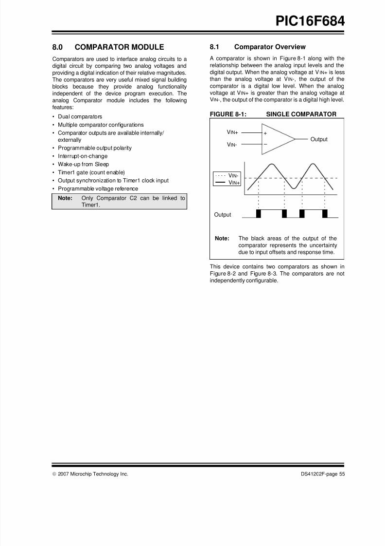
8/10/2019 PIC16F684 Datasheet
http://slidepdf.com/reader/full/pic16f684-datasheet 57/192
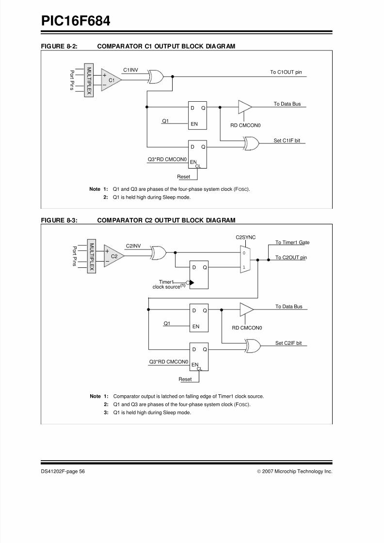
8/10/2019 PIC16F684 Datasheet
http://slidepdf.com/reader/full/pic16f684-datasheet 58/192
PIC16F684
DS41202F-page 56 © 2007 Microchip Technology Inc.
FIGURE 8-2: COMPARATOR C1 OUTPUT BLOCK DIAGRAM
FIGURE 8-3: COMPARATOR C2 OUTPUT BLOCK DIAGRAM
D Q
EN
To C1OUT pin
RD CMCON0
Set C1IF bit
M U L T I P L E X
P or t P i n s
Q3*RD CMCON0
Reset
To Data Bus
C1INV
D Q
ENCL
Q1
Note 1: Q1 and Q3 are phases of the four-phase system clock (FOSC).2: Q1 is held high during Sleep mode.
C1
C2SYNC
D Q
EN
To C2OUT pin
RD CMCON0
Set C2IF bit
M U L T I P L E X
P or t P i n s
Q3*RD CMCON0
Reset
To Data Bus
C2INV
Timer1clock source(1)
0
1
To Timer1 Gate
D Q
D Q
ENCL
Q1
Note 1: Comparator output is latched on falling edge of Timer1 clock source.
2: Q1 and Q3 are phases of the four-phase system clock (FOSC).
3: Q1 is held high during Sleep mode.
C2
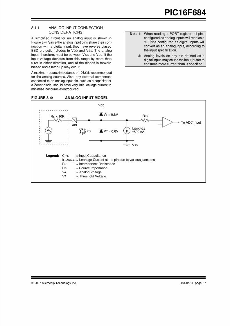
8/10/2019 PIC16F684 Datasheet
http://slidepdf.com/reader/full/pic16f684-datasheet 59/192
© 2007 Microchip Technology Inc. DS41202F-page 57
PIC16F684
8.1.1 ANALOG INPUT CONNECTION
CONSIDERATIONS
A simplified circuit for an analog input is shown in
Figure 8-4. Since the analog input pins share their con-
nection with a digital input, they have reverse biased
ESD protection diodes to VDD and VSS. The analog
input, therefore, must be between VSS and VDD. If the
input voltage deviates from this range by more than
0.6V in either direction, one of the diodes is forward
biased and a latch-up may occur.
A maximum source impedance of 10 kΩ is recommended
for the analog sources. Also, any external component
connected to an analog input pin, such as a capacitor or
a Zener diode, should have very little leakage current to
minimize inaccuracies introduced.
FIGURE 8-4: ANALOG INPUT MODEL
Note 1: When reading a PORT register, all pins
configured as analog inputs will read as a
‘0’. Pins configured as digital inputs will
convert as an analog input, according to
the input specification.
2: Analog levels on any pin defined as adigital input, may cause the input buffer to
consume more current than is specified.
VA
Rs < 10K
CPIN
5 pF
VDD
VT ≈ 0.6V
VT ≈ 0.6V
RIC
ILEAKAGE
±500 nA
Vss
AIN
Legend: CPIN = Input Capacitance
ILEAKAGE = Leakage Current at the pin due to various junctions
RIC = Interconnect Resistance
RS = Source Impedance
VA = Analog VoltageVT = Threshold Voltage
To ADC Input
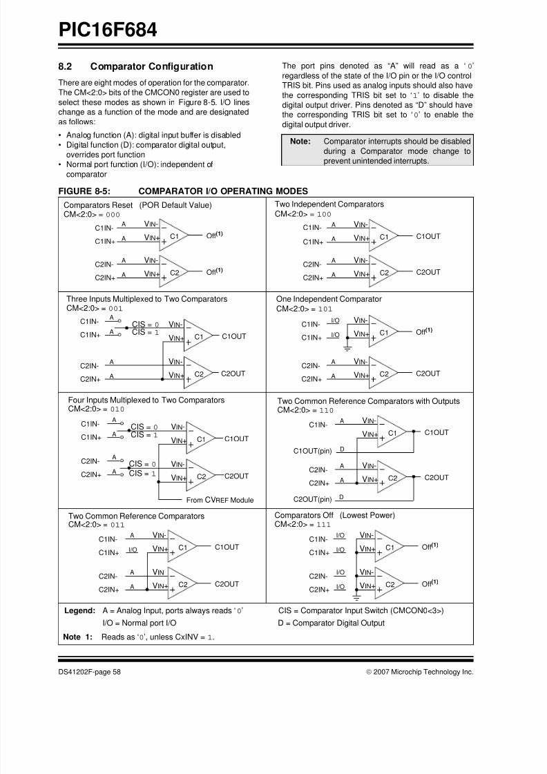
8/10/2019 PIC16F684 Datasheet
http://slidepdf.com/reader/full/pic16f684-datasheet 60/192
PIC16F684
DS41202F-page 58 © 2007 Microchip Technology Inc.
8.2 Comparator Configuration
There are eight modes of operation for the comparator.
The CM<2:0> bits of the CMCON0 register are used to
select these modes as shown in Figure 8-5. I/O lines
change as a function of the mode and are designated
as follows:
• Analog function (A): digital input buffer is disabled• Digital function (D): comparator digital output,
overrides port function
• Normal port function (I/O): independent of
comparator
The port pins denoted as “A” will read as a ‘0’
regardless of the state of the I/O pin or the I/O control
TRIS bit. Pins used as analog inputs should also have
the corresponding TRIS bit set to ‘1’ to disable the
digital output driver. Pins denoted as “D” should have
the corresponding TRIS bit set to ‘0’ to enable the
digital output driver.
FIGURE 8-5: COMPARATOR I/O OPERATING MODES
Note: Comparator interrupts should be disabled
during a Comparator mode change to
prevent unintended interrupts.
C1C1IN-
VIN-
VIN+C1IN+
Off(1)
Comparators Reset (POR Default Value)
A
A
CM<2:0> = 000
C2
C2IN-VIN-
VIN+C2IN+Off(1)
A
A
C1
C1IN- VIN-
VIN+C1IN+
C1OUT
Two Independent Comparators
A
A
CM<2:0> = 100
C2
C2IN-VIN-
VIN+C2IN+C2OUT
A
A
C1C1IN-
VIN-
VIN+C1IN+
C1OUT
Two Common Reference Comparators
A
I/O
CM<2:0> = 011
C2C2IN-
VIN-
VIN+C2IN+
C2OUT
A
A
C1C1IN-
VIN-
VIN+C1IN+
Off(1)
One Independent Comparator
I/O
I/O
CM<2:0> = 101
C2C2IN-
VIN-
VIN+C2IN+
C2OUT
A
A
C1C1IN-
VIN-
VIN+C1IN+
Off(1)
Comparators Off (Lowest Power)
I/O
I/O
CM<2:0> = 111
C2C2IN-
VIN-
VIN+C2IN+
Off(1)
I/O
I/O
C1
C1IN- VIN-
VIN+C1IN+ C1OUT
Four Inputs Multiplexed to Two Comparators
A
A
CM<2:0> = 010
C2
C2IN- VIN-
VIN+C2IN+ C2OUT
A
A
From CVREF Module
CIS = 0CIS = 1
CIS = 0CIS = 1
C1C1IN-
VIN-
VIN+
C1OUT(pin)
C1OUT
Two Common Reference Comparators with Outputs
A
D
CM<2:0> = 110
C2C2IN-
VIN-
VIN+C2IN+
C2OUT
A
A
C2OUT(pin)
C1
C1IN- VIN-
VIN+C1IN+ C1OUT
Three Inputs Multiplexed to Two Comparators
A
A
CM<2:0> = 001
C2C2IN-
VIN-
VIN+C2IN+
C2OUT
A
A
CIS = 0CIS = 1
D
Legend: A = Analog Input, ports always reads ‘0’ CIS = Comparator Input Switch (CMCON0<3>)
I/O = Normal port I/O D = Comparator Digital Output
Note 1: Reads as ‘0’, unless CxINV = 1.
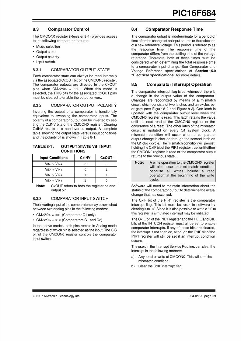
8/10/2019 PIC16F684 Datasheet
http://slidepdf.com/reader/full/pic16f684-datasheet 61/192
© 2007 Microchip Technology Inc. DS41202F-page 59
PIC16F684
8.3 Comparator Control
The CMCON0 register (Register 8-1) provides access
to the following comparator features:
• Mode selection
• Output state
• Output polarity
• Input switch
8.3.1 COMPARATOR OUTPUT STATE
Each comparator state can always be read internally
via the associated CxOUT bit of the CMCON0 register.
The comparator outputs are directed to the CxOUT
pins when CM<2:0> = 110. When this mode is
selected, the TRIS bits for the associated CxOUT pins
must be cleared to enable the output drivers.
8.3.2 COMPARATOR OUTPUT POLARITY
Inverting the output of a comparator is functionally
equivalent to swapping the comparator inputs. The
polarity of a comparator output can be inverted by set-ting the CxINV bits of the CMCON0 register. Clearing
CxINV results in a non-inverted output. A complete
table showing the output state versus input conditions
and the polarity bit is shown in Table 8-1.
TABLE 8-1: OUTPUT STATE VS. INPUTCONDITIONS
8.3.3 COMPARATOR INPUT SWITCH
The inverting input of the comparators may be switched
between two analog pins in the following modes:
• CM<2:0> = 001 (Comparator C1 only)
• CM<2:0> = 010 (Comparators C1 and C2)
In the above modes, both pins remain in Analog mode
regardless of which pin is selected as the input. The CIS
bit of the CMCON0 register controls the comparator
input switch.
8.4 Comparator Response Time
The comparator output is indeterminate for a period of
time after the change of an input source or the selection
of a new reference voltage. This period is referred to as
the response time. The response time of the
comparator differs from the settling time of the voltage
reference. Therefore, both of these times must beconsidered when determining the total response time
to a comparator input change. See Comparator and
Voltage Reference specifications of Section 15.0
“Electrical Specifications” for more details.
8.5 Comparator Interrupt Operation
The comparator interrupt flag is set whenever there is
a change in the output value of the comparator.
Changes are recognized by means of a mismatch
circuit which consists of two latches and an exclusive-
or gate (see Figure 8-2 and Figure 8-3). One latch is
updated with the comparator output level when the
CMCON0 register is read. This latch retains the value
until the next read of the CMCON0 register or the
occurrence of a reset. The other latch of the mismatch
circuit is updated on every Q1 system clock. A
mismatch condition will occur when a comparator
output change is clocked through the second latch on
the Q1 clock cycle. The mismatch condition will persist,
holding the CxIF bit of the PIR1 register true, until either
the CMCON0 register is read or the comparator output
returns to the previous state.
Software will need to maintain information about the
status of the comparator output to determine the actual
change that has occurred.
The CxIF bit of the PIR1 register is the comparator
interrupt flag. This bit must be reset in software by
clearing it to ‘0’. Since it is also possible to write a ‘1’ to
this register, a simulated interrupt may be initiated.
The CxIE bit of the PIE1 register and the PEIE and GIE
bits of the INTCON register must all be set to enable
comparator interrupts. If any of these bits are cleared,
the interrupt is not enabled, although the CxIF bit of the
PIR1 register will still be set if an interrupt condition
occurs.
The user, in the Interrupt Service Routine, can clear the
interrupt in the following manner:
a) Any read or write of CMCON0. This will end the
mismatch condition.
b) Clear the CxIF interrupt flag.
Input Conditions CxINV CxOUT
VIN- > VIN+ 0 0
VIN- < VIN+ 0 1
VIN- > VIN+ 1 1
VIN- < VIN+ 1 0
Note: CxOUT refers to both the register bit and
output pin.
Note: A write operation to the CMCON0 register
will also clear the mismatch condition
because all writes include a read
operation at the beginning of the write
cycle.
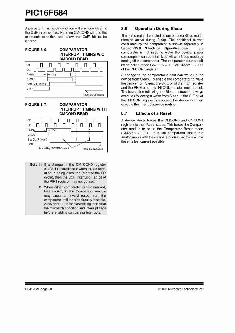
8/10/2019 PIC16F684 Datasheet
http://slidepdf.com/reader/full/pic16f684-datasheet 62/192
PIC16F684
DS41202F-page 60 © 2007 Microchip Technology Inc.
A persistent mismatch condition will preclude clearing
the CxIF interrupt flag. Reading CMCON0 will end the
mismatch condition and allow the CxIF bit to be
cleared.
FIGURE 8-6: COMPARATOR
INTERRUPT TIMING W/O
CMCON0 READ
FIGURE 8-7: COMPARATORINTERRUPT TIMING WITH
CMCON0 READ
8.6 Operation During Sleep
The comparator, if enabled before entering Sleep mode,
remains active during Sleep. The additional current
consumed by the comparator is shown separately in
Section 15.0 “Electrical Specifications”. If the
comparator is not used to wake the device, power
consumption can be minimized while in Sleep mode byturning off the comparator. The comparator is turned off
by selecting mode CM<2:0> = 000 or CM<2:0> = 111
of the CMCON0 register.
A change to the comparator output can wake-up the
device from Sleep. To enable the comparator to wake
the device from Sleep, the CxIE bit of the PIE1 register
and the PEIE bit of the INTCON register must be set.
The instruction following the Sleep instruction always
executes following a wake from Sleep. If the GIE bit of
the INTCON register is also set, the device will then
execute the interrupt service routine.
8.7 Effects of a Reset
A device Reset forces the CMCON0 and CMCON1
registers to their Reset states. This forces the Compar-
ator module to be in the Comparator Reset mode
(CM<2:0> = 000). Thus, all comparator inputs are
analog inputs with the comparator disabled to consume
the smallest current possible.
Note 1: If a change in the CM1CON0 register
(CxOUT) should occur when a read oper-
ation is being executed (start of the Q2
cycle), then the CxIF Interrupt Flag bit of
the PIR1 register may not get set.
2: When either comparator is first enabled,
bias circuitry in the Comparator module
may cause an invalid output from the
comparator until the bias circuitry is stable.
Allow about 1 µs for bias settling then clear
the mismatch condition and interrupt flags
before enabling comparator interrupts.
Q1
Q3
CxIN+
CxOUT
Set CMIF (level)
CMIF
TRT
reset by software
Q1
Q3
CxIN+
CxOUT
Set CMIF (level)
CMIF
TRT
reset by softwarecleared by CMCON0 read
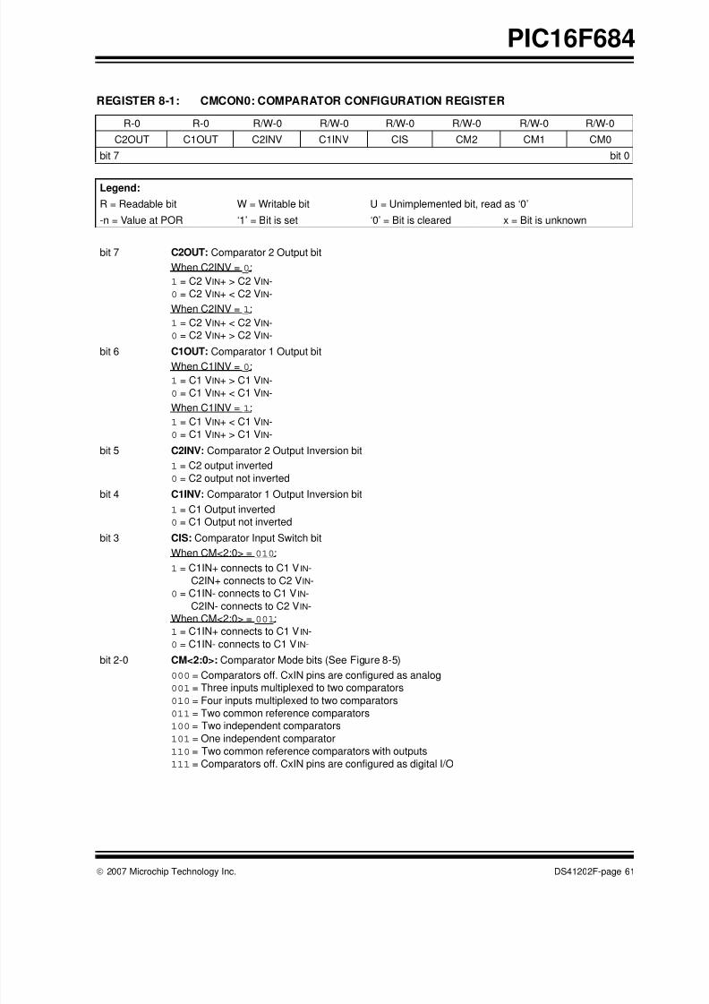
8/10/2019 PIC16F684 Datasheet
http://slidepdf.com/reader/full/pic16f684-datasheet 63/192
© 2007 Microchip Technology Inc. DS41202F-page 61
PIC16F684
REGISTER 8-1: CMCON0: COMPARATOR CONFIGURATION REGISTER
R-0 R-0 R/W-0 R/W-0 R/W-0 R/W-0 R/W-0 R/W-0
C2OUT C1OUT C2INV C1INV CIS CM2 CM1 CM0
bit 7 bit 0
Legend:
R = Readable bit W = Writable bit U = Unimplemented bit, read as ‘0’
-n = Value at POR ‘1’ = Bit is set ‘0’ = Bit is cleared x = Bit is unknown
bit 7 C2OUT: Comparator 2 Output bit
When C2INV = 0:
1 = C2 VIN+ > C2 VIN-
0 = C2 VIN+ < C2 VIN-
When C2INV = 1:
1 = C2 VIN+ < C2 VIN-
0 = C2 VIN+ > C2 VIN-
bit 6 C1OUT: Comparator 1 Output bitWhen C1INV = 0:
1 = C1 VIN+ > C1 VIN-
0 = C1 VIN+ < C1 VIN-
When C1INV = 1:
1 = C1 VIN+ < C1 VIN-
0 = C1 VIN+ > C1 VIN-
bit 5 C2INV: Comparator 2 Output Inversion bit
1 = C2 output inverted
0 = C2 output not inverted
bit 4 C1INV: Comparator 1 Output Inversion bit
1 = C1 Output inverted
0 = C1 Output not inverted
bit 3 CIS: Comparator Input Switch bit
When CM<2:0> = 010:
1 = C1IN+ connects to C1 VIN-
C2IN+ connects to C2 VIN-
0 = C1IN- connects to C1 VIN-
C2IN- connects to C2 VIN-
When CM<2:0> = 001:
1 = C1IN+ connects to C1 VIN-
0 = C1IN- connects to C1 VIN-
bit 2-0 CM<2:0>: Comparator Mode bits (See Figure 8-5)
000 = Comparators off. CxIN pins are configured as analog
001 = Three inputs multiplexed to two comparators
010 = Four inputs multiplexed to two comparators011 = Two common reference comparators
100 = Two independent comparators
101 = One independent comparator
110 = Two common reference comparators with outputs
111 = Comparators off. CxIN pins are configured as digital I/O
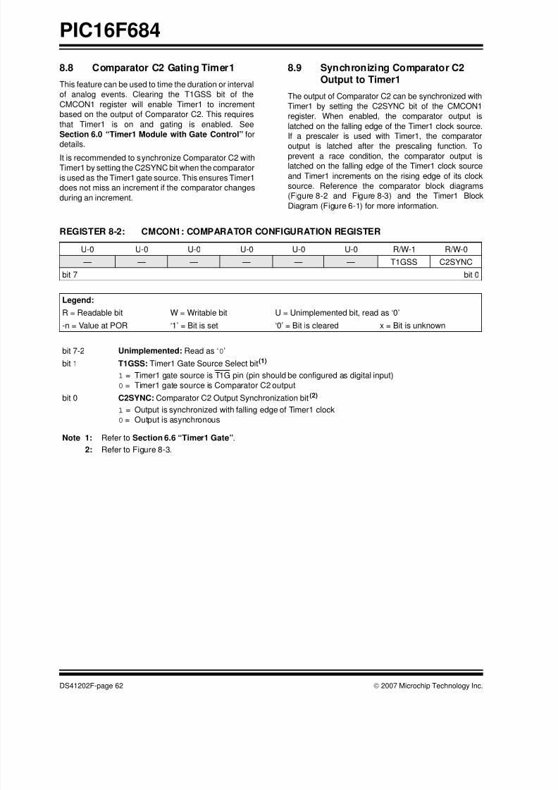
8/10/2019 PIC16F684 Datasheet
http://slidepdf.com/reader/full/pic16f684-datasheet 64/192
PIC16F684
DS41202F-page 62 © 2007 Microchip Technology Inc.
8.8 Comparator C2 Gating Timer1
This feature can be used to time the duration or interval
of analog events. Clearing the T1GSS bit of the
CMCON1 register will enable Timer1 to increment
based on the output of Comparator C2. This requires
that Timer1 is on and gating is enabled. See
Section 6.0 “Timer1 Module with Gate Control” fordetails.
It is recommended to synchronize Comparator C2 with
Timer1 by setting the C2SYNC bit when the comparator
is used as the Timer1 gate source. This ensures Timer1
does not miss an increment if the comparator changes
during an increment.
8.9 Synchronizing Comparator C2Output to Timer1
The output of Comparator C2 can be synchronized with
Timer1 by setting the C2SYNC bit of the CMCON1
register. When enabled, the comparator output is
latched on the falling edge of the Timer1 clock source.
If a prescaler is used with Timer1, the comparatoroutput is latched after the prescaling function. To
prevent a race condition, the comparator output is
latched on the falling edge of the Timer1 clock source
and Timer1 increments on the rising edge of its clock
source. Reference the comparator block diagrams
(Figure 8-2 and Figure 8-3) and the Timer1 Block
Diagram (Figure 6-1) for more information.
REGISTER 8-2: CMCON1: COMPARATOR CONFIGURATION REGISTER
U-0 U-0 U-0 U-0 U-0 U-0 R/W-1 R/W-0
— — — — — — T1GSS C2SYNC
bit 7 bit 0
Legend:
R = Readable bit W = Writable bit U = Unimplemented bit, read as ‘0’
-n = Value at POR ‘1’ = Bit is set ‘0’ = Bit is cleared x = Bit is unknown
bit 7-2 Unimplemented: Read as ‘0’
bit 1 T1GSS: Timer1 Gate Source Select bit(1)
1 = Timer1 gate source is T1G pin (pin should be configured as digital input)
0 = Timer1 gate source is Comparator C2 output
bit 0 C2SYNC: Comparator C2 Output Synchronization bit(2)
1 = Output is synchronized with falling edge of Timer1 clock
0 = Output is asynchronous
Note 1: Refer to Section 6.6 “Timer1 Gate”.
2: Refer to Figure 8-3.

8/10/2019 PIC16F684 Datasheet
http://slidepdf.com/reader/full/pic16f684-datasheet 65/192
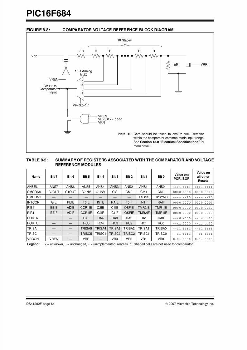
8/10/2019 PIC16F684 Datasheet
http://slidepdf.com/reader/full/pic16f684-datasheet 66/192
PIC16F684
DS41202F-page 64 © 2007 Microchip Technology Inc.
FIGURE 8-8: COMPARATOR VOLTAGE REFERENCE BLOCK DIAGRAM
TABLE 8-2: SUMMARY OF REGISTERS ASSOCIATED WITH THE COMPARATOR AND VOLTAGEREFERENCE MODULES
Name Bit 7 Bit 6 Bit 5 Bit 4 Bit 3 Bit 2 Bit 1 Bit 0Value on:
POR, BOR
Value on
all other
Resets
ANSEL ANS7 ANS6 ANS5 ANS4 ANS3 ANS2 ANS1 ANS0 1111 1111 1111 1111
CMCON0 C2OUT C1OUT C2INV C1INV CIS CM2 CM1 CM0 0000 0000 0000 0000
CMCON1 — — — — — — T1GSS C2SYNC ---- --10 ---- --10
INTCON GIE PEIE T0IE INTE RAIE T0IF INTF RAIF 0000 0000 0000 0000
PIE1 EEIE ADIE CCP1IE C2IE C1IE OSFIE TMR2IE TMR1IE 0000 0000 0000 0000
PIR1 EEIF ADIF CCP1IF C2IF C1IF OSFIF TMR2IF TMR1IF 0000 0000 0000 0000
PORTA — — RA5 RA4 RA3 RA2 RA1 RA0 --x0 x000 --uu uu00
PORTC — — RC5 RC4 RC3 RC2 RC1 RC0 --xx 0000 --uu uu00
TRISA — — TRISA5 TRISA4 TRISA3 TRISA2 TRISA1 TRISA0 --11 1111 --11 1111
TRISC — — TRISC5 TRISC4 TRISC3 TRISC2 TRISC1 TRISC0 --11 1111 --11 1111
VRCON VREN — VRR — VR3 VR2 VR1 VR0 0-0- 0000 0-0- 0000
Legend: x = unknown, u = unchanged, - = unimplemented, read as ‘0’. Shaded cells are not used for comparator.
VRR8R
VR<3:0>(1)
16-1 Analog
8R R R R R
CVREF to
16 Stages
ComparatorInput
VREN
VDD
MUX
VR<3:0> = 0000VREN
VRR
0
12
14
15
Note 1: Care should be taken to ensure VREF remains
within the comparator common mode input range.
See Section 15.0 “Electrical Specifications” for
more detail.

8/10/2019 PIC16F684 Datasheet
http://slidepdf.com/reader/full/pic16f684-datasheet 67/192
© 2007 Microchip Technology Inc. DS41202F-page 65
PIC16F684
9.0 ANALOG-TO-DIGITALCONVERTER (ADC) MODULE
The Analog-to-Digital Converter (ADC) allows
conversion of an analog input signal to a 10-bit binary
representation of that signal. This device uses analog
inputs, which are multiplexed into a single sample and
hold circuit. The output of the sample and hold isconnected to the input of the converter. The converter
generates a 10-bit binary result via successive
approximation and stores the conversion result into the
ADC result registers (ADRESL and ADRESH).
The ADC voltage reference is software selectable to
either VDD or a voltage applied to the external reference
pins.
The ADC can generate an interrupt upon completion of
a conversion. This interrupt can be used to wake-up the
device from Sleep.
Figure 9-1 shows the block diagram of the ADC.
FIGURE 9-1: ADC BLOCK DIAGRAM
RA0/AN0
A/DRA1/AN1/VREF
RA2/AN2
RC0/AN4
VDD
VREF
ADON
GO/DONE
VCFG = 1
VCFG = 0
CHS <3:0>
VSS
RC1/AN5
RC2/AN6
RC3/AN7
RA4/AN3
ADRESH ADRESL
10
10
ADFM0 = Left Justify
1 = Right Justify
4
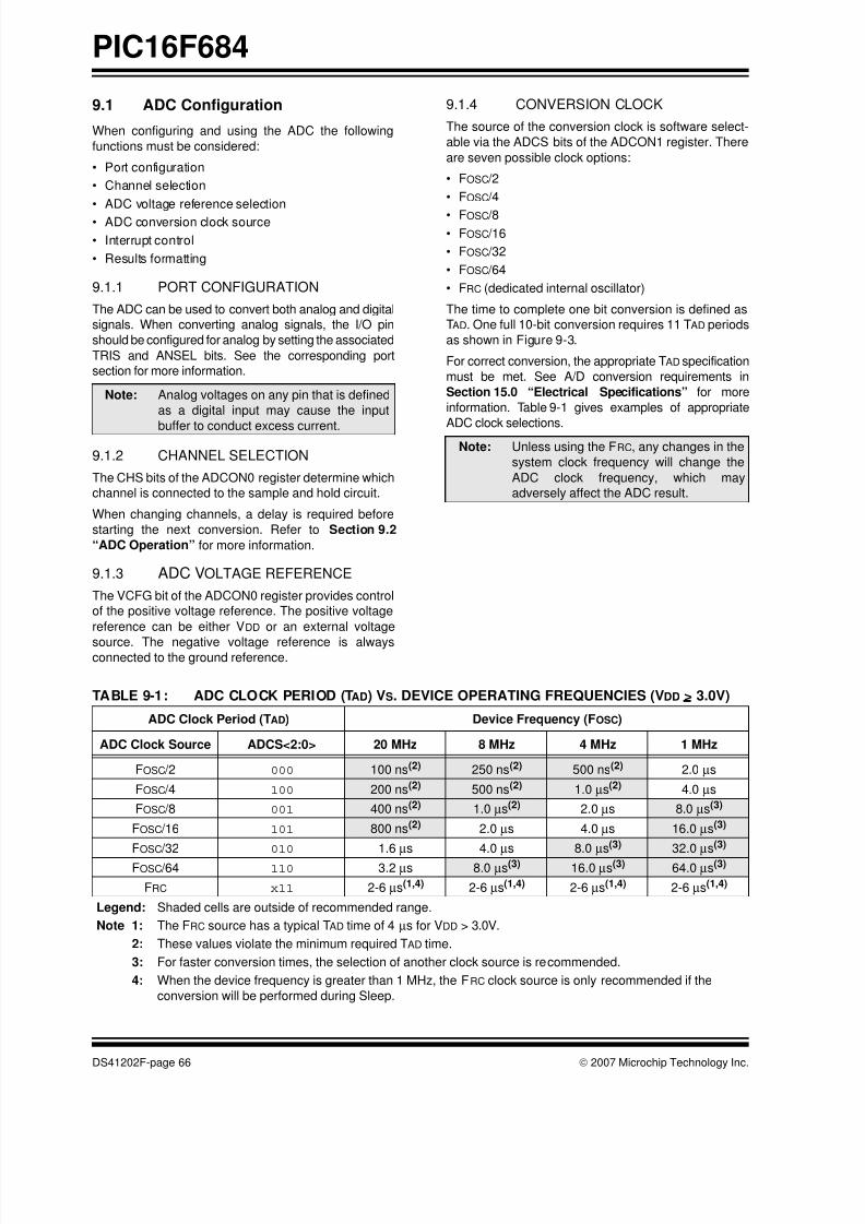
8/10/2019 PIC16F684 Datasheet
http://slidepdf.com/reader/full/pic16f684-datasheet 68/192
PIC16F684
DS41202F-page 66 © 2007 Microchip Technology Inc.
9.1 ADC Configuration
When configuring and using the ADC the following
functions must be considered:
• Port configuration
• Channel selection
• ADC voltage reference selection
• ADC conversion clock source
• Interrupt control
• Results formatting
9.1.1 PORT CONFIGURATION
The ADC can be used to convert both analog and digital
signals. When converting analog signals, the I/O pin
should be configured for analog by setting the associated
TRIS and ANSEL bits. See the corresponding port
section for more information.
9.1.2 CHANNEL SELECTION
The CHS bits of the ADCON0 register determine which
channel is connected to the sample and hold circuit.
When changing channels, a delay is required before
starting the next conversion. Refer to Section 9.2
“ADC Operation” for more information.
9.1.3 ADC VOLTAGE REFERENCE
The VCFG bit of the ADCON0 register provides control
of the positive voltage reference. The positive voltage
reference can be either VDD or an external voltage
source. The negative voltage reference is alwaysconnected to the ground reference.
9.1.4 CONVERSION CLOCK
The source of the conversion clock is software select-
able via the ADCS bits of the ADCON1 register. There
are seven possible clock options:
• FOSC /2
• FOSC /4
• FOSC /8• FOSC /16
• FOSC /32
• FOSC /64
• FRC (dedicated internal oscillator)
The time to complete one bit conversion is defined as
TAD. One full 10-bit conversion requires 11 TAD periods
as shown in Figure 9-3.
For correct conversion, the appropriate TAD specification
must be met. See A/D conversion requirements in
Section 15.0 “Electrical Specifications” for more
information. Table 9-1 gives examples of appropriate
ADC clock selections.
TABLE 9-1: ADC CLOCK PERIOD (TAD) VS. DEVICE OPERATING FREQUENCIES (VDD > 3.0V)
Note: Analog voltages on any pin that is defined
as a digital input may cause the input
buffer to conduct excess current.Note: Unless using the FRC, any changes in the
system clock frequency will change the
ADC clock frequency, which may
adversely affect the ADC result.
ADC Clock Period (TAD) Device Frequency (FOSC)
ADC Clock Source ADCS<2:0> 20 MHz 8 MHz 4 MHz 1 MHz
FOSC /2 000 100 ns(2) 250 ns(2) 500 ns(2) 2.0 µs
FOSC /4 100 200 ns(2) 500 ns(2) 1.0 µs(2) 4.0 µs
FOSC /8 001 400 ns(2) 1.0 µs(2) 2.0 µs 8.0 µs(3)
FOSC /16 101 800 ns(2) 2.0 µs 4.0 µs 16.0 µs(3)
FOSC /32 010 1.6 µs 4.0 µs 8.0 µs(3) 32.0 µs(3)
FOSC /64 110 3.2 µs 8.0 µs(3) 16.0 µs(3) 64.0 µs(3)
FRC x11 2-6 µs(1,4) 2-6 µs(1,4) 2-6 µs(1,4) 2-6 µs(1,4)
Legend: Shaded cells are outside of recommended range.
Note 1: The FRC source has a typical TAD time of 4 µs for VDD > 3.0V.
2: These values violate the minimum required TAD time.
3: For faster conversion times, the selection of another clock source is recommended.
4: When the device frequency is greater than 1 MHz, the FRC clock source is only recommended if the
conversion will be performed during Sleep.

8/10/2019 PIC16F684 Datasheet
http://slidepdf.com/reader/full/pic16f684-datasheet 69/192
© 2007 Microchip Technology Inc. DS41202F-page 67
PIC16F684
FIGURE 9-2: ANALOG-TO-DIGITAL CONVERSION TAD CYCLES
9.1.5 INTERRUPTS
The ADC module allows for the ability to generate an
interrupt upon completion of an analog-to-digital
conversion. The ADC interrupt flag is the ADIF bit in the
PIR1 register. The ADC interrupt enable is the ADIE bit
in the PIE1 register. The ADIF bit must be cleared insoftware.
This interrupt can be generated while the device is
operating or while in Sleep. If the device is in Sleep, the
interrupt will wake-up the device. Upon waking from
Sleep, the next instruction following the SLEEP
instruction is always executed. If the user is attempting
to wake-up from Sleep and resume in-line code
execution, the global interrupt must be disabled. If the
global interrupt is enabled, execution will switch to the
interrupt service routine.Please see Section 9.1.5 “Interrupts” for more
information.
9.1.6 RESULT FORMATTING
The 10-bit A/D conversion result can be supplied in two
formats, left justified or right justified. The ADFM bit of
the ADCON0 register controls the output format.
Figure 9-4 shows the two output formats.
FIGURE 9-3: 10-BIT A/D CONVERSION RESULT FORMAT
TAD1 TAD2 TAD3 TAD4 TAD5 TAD6 TAD7 TAD8 TAD9
Set GO/DONE bit
Holding Capacitor is Disconnected from Analog Input (typically 100 ns)
b9 b8 b7 b6 b5 b4 b3 b2
TAD10 TAD11
b1 b0
TCY to TAD
Conversion Starts
ADRESH and ADRESL registers are loaded,
GO bit is cleared,
ADIF bit is set,
Holding capacitor is connected to analog input
Note: The ADIF bit is set at the completion of
every conversion, regardless of whether
or not the ADC interrupt is enabled.
ADRESH ADRESL
(ADFM = 0) MSB LSB
bit 7 bit 0 bit 7 bit 0
10-bit A/D Result Unimplemented: Read as ‘0’
(ADFM = 1) MSB LSBbit 7 bit 0 bit 7 bit 0
Unimplemented: Read as ‘0’ 10-bit A/D Result

8/10/2019 PIC16F684 Datasheet
http://slidepdf.com/reader/full/pic16f684-datasheet 70/192
PIC16F684
DS41202F-page 68 © 2007 Microchip Technology Inc.
9.2 ADC Operation
9.2.1 STARTING A CONVERSION
To enable the ADC module, the ADON bit of the
ADCON0 register must be set to a ‘1’. Setting the
GO/DONE bit of the ADCON0 register to a ‘1’ will start
the analog-to-digital conversion.
9.2.2 COMPLETION OF A CONVERSION
When the conversion is complete, the ADC module will:
• Clear the GO/DONE bit
• Set the ADIF flag bit
• Update the ADRESH:ADRESL registers with new
conversion result
9.2.3 TERMINATING A CONVERSIONIf a conversion must be terminated before completion,
the GO/DONE bit can be cleared in software. The
ADRESH:ADRESL registers will not be updated with
the partially complete analog-to-digital conversion
sample. Instead, the ADRESH:ADRESL register pair
will retain the value of the previous conversion. Addi-
tionally, a 2 TAD delay is required before another acqui-
sition can be initiated. Following this delay, an input
acquisition is automatically started on the selected
channel.
9.2.4 ADC OPERATION DURING SLEEP
The ADC module can operate during Sleep. This
requires the ADC clock source to be set to the FRC
option. When the FRC clock source is selected, the
ADC waits one additional instruction before starting the
conversion. This allows the SLEEP instruction to be
executed, which can reduce system noise during the
conversion. If the ADC interrupt is enabled, the device
will wake-up from Sleep when the conversion
completes. If the ADC interrupt is disabled, the ADC
module is turned off after the conversion completes,
although the ADON bit remains set.
When the ADC clock source is something other than
FRC, a SLEEP instruction causes the present conver-
sion to be aborted and the ADC module is turned off,
although the ADON bit remains set.
9.2.5 SPECIAL EVENT TRIGGER
The ECCP Special Event Trigger allows periodic ADC
measurements without software intervention. When
this trigger occurs, the GO/DONE bit is set by hardware
and the Timer1 counter resets to zero.
Using the Special Event Trigger does not ensure
proper ADC timing. It is the user’s responsibility toensure that the ADC timing requirements are met.
See Section 11.0 “Enhanced Capture/Com-
pare/PWM (With Auto-Shutdown and Dead Band)
Module” for more information.
9.2.6 A/D CONVERSION PROCEDURE
This is an example procedure for using the ADC to
perform an Analog-to-Digital conversion:
1. Configure Port:
• Disable pin output driver (See TRIS register)
• Configure pin as analog
2. Configure the ADC module:
• Select ADC conversion clock
• Configure voltage reference
• Select ADC input channel
• Select result format
• Turn on ADC module
3. Configure ADC interrupt (optional):
• Clear ADC interrupt flag
• Enable ADC interrupt
• Enable peripheral interrupt
• Enable global interrupt(1)
4. Wait the required acquisition time(2).
5. Start conversion by setting the GO/DONE bit.6. Wait for ADC conversion to complete by one of
the following:
• Polling the GO/DONE bit
• Waiting for the ADC interrupt (interrupts
enabled)
7. Read ADC Result
8. Clear the ADC interrupt flag (required if interrupt
is enabled).
Note: The GO/DONE bit should not be set in the
same instruction that turns on the ADC.
Refer to Section 9.2.6 “A/D Conversion
Procedure”.
Note: A device Reset forces all registers to their
Reset state. Thus, the ADC module is
turned off and any pending conversion isterminated.
Note 1: The global interrupt can be disabled if the
user is attempting to wake-up from Sleep
and resume in-line code execution.
2: See Section 9.3 “A/D Acquisition
Requirements”.

8/10/2019 PIC16F684 Datasheet
http://slidepdf.com/reader/full/pic16f684-datasheet 71/192
© 2007 Microchip Technology Inc. DS41202F-page 69
PIC16F684
EXAMPLE 9-1: A/D CONVERSION
;This code block configures the ADC
;for polling, Vdd reference, Frc clock
;and AN0 input.
;
;Conversion start & polling for completion
; are included.
;BANKSEL ADCON1 ;
MOVLW B’01110000’ ;ADC Frc clock
MOVWF ADCON1 ;
BANKSEL TRISA ;
BSF TRISA,0 ;Set RA0 to input
BANKSEL ANSEL ;
BSF ANSEL,0 ;Set RA0 to analog
BANKSEL ADCON0 ;
MOVLW B’10000001’ ;Right justify,
MOVWF ADCON0 ; Vdd Vref, AN0, On
CALL SampleTime ;Acquisiton delay
BSF ADCON0,GO ;Start conversion
BTFSC ADCON0,GO ;Is conversion done?
GOTO $-1 ;No, test again
BANKSEL ADRESH ;MOVF ADRESH,W ;Read upper 2 bits
MOVWF RESULTHI ;store in GPR space
BANKSEL ADRESL ;
MOVF ADRESL,W ;Read lower 8 bits
MOVWF RESULTLO ;Store in GPR space

8/10/2019 PIC16F684 Datasheet
http://slidepdf.com/reader/full/pic16f684-datasheet 72/192
PIC16F684
DS41202F-page 70 © 2007 Microchip Technology Inc.
9.2.7 ADC REGISTER DEFINITIONS
The following registers are used to control the operation of the ADC.
REGISTER 9-1: ADCON0: A/D CONTROL REGISTER 0
R/W-0 R/W-0 U-0 R/W-0 R/W-0 R/W-0 R/W-0 R/W-0
ADFM VCFG — CHS2 CHS1 CHS0 GO/DONE ADONbit 7 bit 0
Legend:
R = Readable bit W = Writable bit U = Unimplemented bit, read as ‘0’
-n = Value at POR ‘1’ = Bit is set ‘0’ = Bit is cleared x = Bit is unknown
bit 7 ADFM: A/D Conversion Result Format Select bit
1 = Right justified
0 = Left justified
bit 6 VCFG: Voltage Reference bit
1 = VREF pin
0 = VDD
bit 5 Unimplemented: Read as ‘0’
bit 4-2 CHS<2:0>: Analog Channel Select bits
000 = AN0
001 = AN1
010 = AN2
011 = AN3
100 = AN4
101 = AN5
110 = AN6
111 = AN7
bit 1 GO/DONE: A/D Conversion Status bit
1 = A/D conversion cycle in progress. Setting this bit starts an A/D conversion cycle.
This bit is automatically cleared by hardware when the A/D conversion has completed.
0 = A/D conversion completed/not in progress
bit 0 ADON: ADC Enable bit1 = ADC is enabled
0 = ADC is disabled and consumes no operating current
REGISTER 9-2: ADCON1: A/D CONTROL REGISTER 1
U-0 R/W-0 R/W-0 R/W-0 U-0 U-0 U-0 U-0
— ADCS2 ADCS1 ADCS0 — — — —
bit 7 bit 0
Legend:
R = Readable bit W = Writable bit U = Unimplemented bit, read as ‘0’
-n = Value at POR ‘1’ = Bit is set ‘0’ = Bit is cleared x = Bit is unknown
bit 7 Unimplemented: Read as ‘0’
bit 6-4 ADCS<2:0>: A/D Conversion Clock Select bits
000 = FOSC /2
001 = FOSC /8
010 = FOSC /32
x11 = FRC (clock derived from a dedicated internal oscillator = 500 kHz max)
100 = FOSC /4
101 = FOSC /16
110 = FOSC /64
bit 3-0 Unimplemented: Read as ‘0’

8/10/2019 PIC16F684 Datasheet
http://slidepdf.com/reader/full/pic16f684-datasheet 73/192
© 2007 Microchip Technology Inc. DS41202F-page 71
PIC16F684
REGISTER 9-3: ADRESH: ADC RESULT REGISTER HIGH (ADRESH) ADFM = 0
R/W-x R/W-x R/W-x R/W-x R/W-x R/W-x R/W-x R/W-x
ADRES9 ADRES8 ADRES7 ADRES6 ADRES5 ADRES4 ADRES3 ADRES2
bit 7 bit 0
Legend:
R = Readable bit W = Writable bit U = Unimplemented bit, read as ‘0’
-n = Value at POR ‘1’ = Bit is set ‘0’ = Bit is cleared x = Bit is unknown
bit 7-0 ADRES<9:2>: ADC Result Register bits
Upper 8 bits of 10-bit conversion result
REGISTER 9-4: ADRESL: ADC RESULT REGISTER LOW (ADRESL) ADFM = 0
R/W-x R/W-x R/W-x R/W-x R/W-x R/W-x R/W-x R/W-x
ADRES1 ADRES0 — — — — — —
bit 7 bit 0
Legend:
R = Readable bit W = Writable bit U = Unimplemented bit, read as ‘0’
-n = Value at POR ‘1’ = Bit is set ‘0’ = Bit is cleared x = Bit is unknown
bit 7-6 ADRES<1:0>: ADC Result Register bits
Lower 2 bits of 10-bit conversion result
bit 5-0 Reserved: Do not use.
REGISTER 9-5: ADRESH: ADC RESULT REGISTER HIGH (ADRESH) ADFM = 1
R/W-x R/W-x R/W-x R/W-x R/W-x R/W-x R/W-x R/W-x
— — — — — — ADRES9 ADRES8
bit 7 bit 0
Legend:
R = Readable bit W = Writable bit U = Unimplemented bit, read as ‘0’
-n = Value at POR ‘1’ = Bit is set ‘0’ = Bit is cleared x = Bit is unknown
bit 7-2 Reserved: Do not use.
bit 1-0 ADRES<9:8>: ADC Result Register bits
Upper 2 bits of 10-bit conversion result
REGISTER 9-6: ADRESL: ADC RESULT REGISTER LOW (ADRESL) ADFM = 1
R/W-x R/W-x R/W-x R/W-x R/W-x R/W-x R/W-x R/W-x
ADRES7 ADRES6 ADRES5 ADRES4 ADRES3 ADRES2 ADRES1 ADRES0
bit 7 bit 0
Legend:
R = Readable bit W = Writable bit U = Unimplemented bit, read as ‘0’
-n = Value at POR ‘1’ = Bit is set ‘0’ = Bit is cleared x = Bit is unknown
bit 7-0 ADRES<7:0>: ADC Result Register bits
Lower 8 bits of 10-bit conversion result
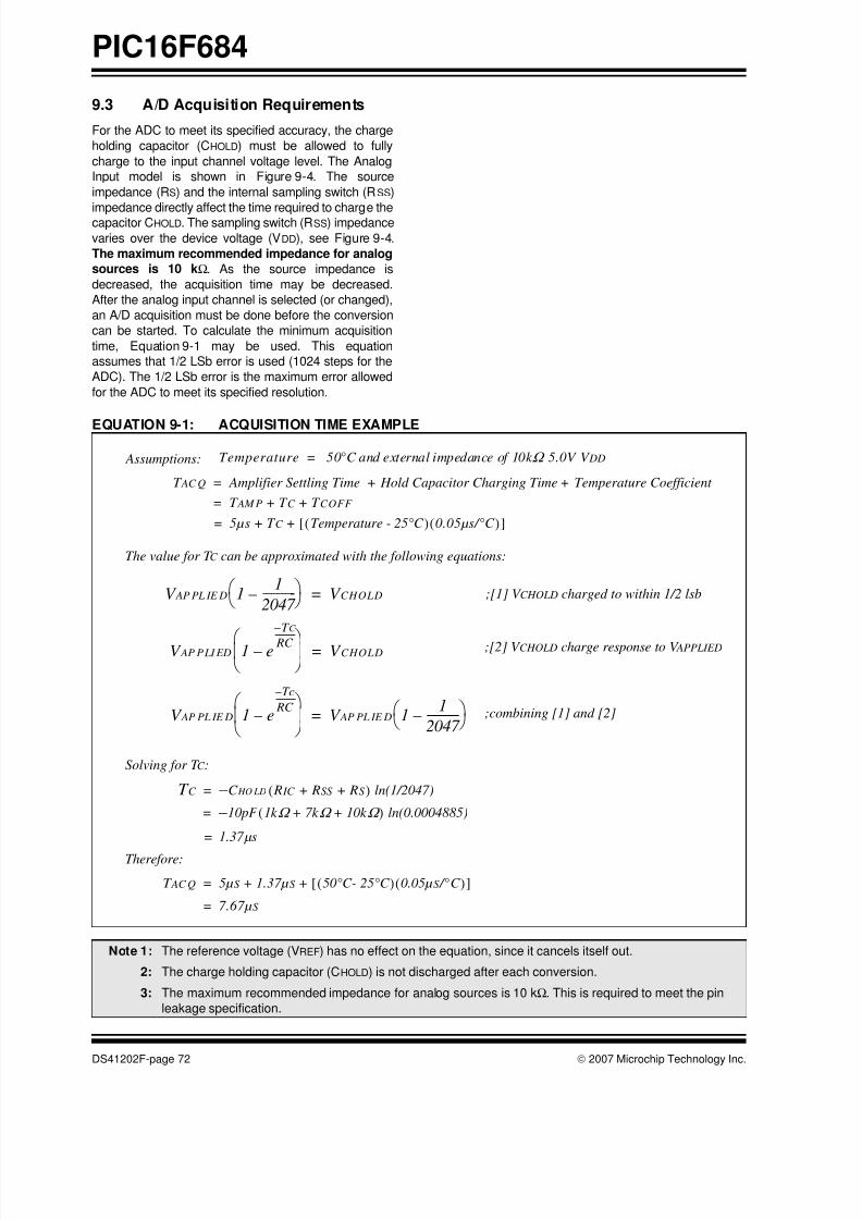
8/10/2019 PIC16F684 Datasheet
http://slidepdf.com/reader/full/pic16f684-datasheet 74/192
PIC16F684
DS41202F-page 72 © 2007 Microchip Technology Inc.
9.3 A/D Acquisition Requirements
For the ADC to meet its specified accuracy, the charge
holding capacitor (CHOLD) must be allowed to fully
charge to the input channel voltage level. The Analog
Input model is shown in Figure 9-4. The source
impedance (RS) and the internal sampling switch (RSS)
impedance directly affect the time required to charge thecapacitor CHOLD. The sampling switch (RSS) impedance
varies over the device voltage (VDD), see Figure 9-4.
The maximum recommended impedance for analog
sources is 10 kΩ. As the source impedance is
decreased, the acquisition time may be decreased.
After the analog input channel is selected (or changed),
an A/D acquisition must be done before the conversion
can be started. To calculate the minimum acquisition
time, Equation 9-1 may be used. This equation
assumes that 1/2 LSb error is used (1024 steps for the
ADC). The 1/2 LSb error is the maximum error allowed
for the ADC to meet its specified resolution.
EQUATION 9-1: ACQUISITION TIME EXAMPLE
T AC Q Amplifier Settling Time Hold Capacitor Charging Time Temperature Coefficient + +=
T AM P T C T COFF + +=
5µs T C Temperature - 25°C ( ) 0.05µs/°C ( )[ ]+ +=
T C C HO LD R IC RSS RS + +( ) ln(1/2047)–=
10pF 1k Ω 7k Ω 10k Ω + +( )– ln(0.0004885)=
1.37 = µs
T AC Q 5µS 1.37µS 50°C- 25°C ( ) 0.05µS /°C ( )[ ]+ +=
7.67µS =
V AP PL IE D 1 e
Tc–
RC ---------
–⎝ ⎠⎜ ⎟⎛ ⎞
V AP PL IE D 11
2047 ------------–⎝ ⎠
⎛ ⎞=
V AP PL IE D 11
2047 ------------–⎝ ⎠
⎛ ⎞ V CHOLD=
V AP PLI ED 1 e
T C –
RC ----------
–⎝ ⎠⎜ ⎟⎛ ⎞ V CHOLD=
;[1] V CHOLD charged to within 1/2 lsb
;[2] V CHOLD charge response to V APPLIED
;combining [1] and [2]
The value for T C can be approximated with the following equations:
Solving for T C :
Therefore:
Temperature 50°C and external impedance of 10k Ω 5.0V V DD= Assumptions:
Note 1: The reference voltage (VREF) has no effect on the equation, since it cancels itself out.
2: The charge holding capacitor (CHOLD) is not discharged after each conversion.
3: The maximum recommended impedance for analog sources is 10 kΩ. This is required to meet the pin
leakage specification.
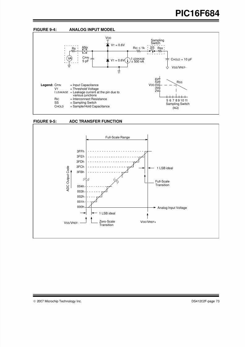
8/10/2019 PIC16F684 Datasheet
http://slidepdf.com/reader/full/pic16f684-datasheet 75/192
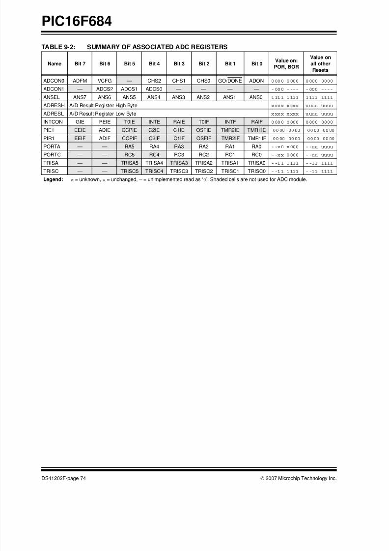
8/10/2019 PIC16F684 Datasheet
http://slidepdf.com/reader/full/pic16f684-datasheet 76/192
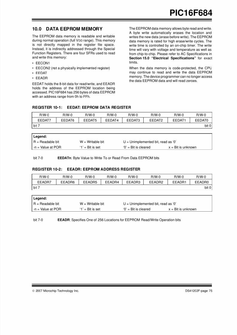
8/10/2019 PIC16F684 Datasheet
http://slidepdf.com/reader/full/pic16f684-datasheet 77/192
© 2007 Microchip Technology Inc. DS41202F-page 75
PIC16F684
10.0 DATA EEPROM MEMORY
The EEPROM data memory is readable and writable
during normal operation (full VDD range). This memory
is not directly mapped in the register file space.
Instead, it is indirectly addressed through the Special
Function Registers. There are four SFRs used to read
and write this memory:• EECON1
• EECON2 (not a physically implemented register)
• EEDAT
• EEADR
EEDAT holds the 8-bit data for read/write, and EEADR
holds the address of the EEPROM location being
accessed. PIC16F684 has 256 bytes of data EEPROM
with an address range from 0h to FFh.
The EEPROM data memory allows byte read and write.
A byte write automatically erases the location and
writes the new data (erase before write). The EEPROM
data memory is rated for high erase/write cycles. The
write time is controlled by an on-chip timer. The write
time will vary with voltage and temperature as well as
from chip-to-chip. Please refer to AC Specifications in
Section 15.0 “Electrical Specifications” for exactlimits.
When the data memory is code-protected, the CPU
may continue to read and write the data EEPROM
memory. The device programmer can no longer access
the data EEPROM data and will read zeroes.
REGISTER 10-1: EEDAT: EEPROM DATA REGISTER
R/W-0 R/W-0 R/W-0 R/W-0 R/W-0 R/W-0 R/W-0 R/W-0
EEDAT7 EEDAT6 EEDAT5 EEDAT4 EEDAT3 EEDAT2 EEDAT1 EEDAT0
bit 7 bit 0
Legend:
R = Readable bit W = Writable bit U = Unimplemented bit, read as ‘0’
-n = Value at POR ‘1’ = Bit is set ‘0’ = Bit is cleared x = Bit is unknown
bit 7-0 EEDATn: Byte Value to Write To or Read From Data EEPROM bits
REGISTER 10-2: EEADR: EEPROM ADDRESS REGISTER
R/W-0 R/W-0 R/W-0 R/W-0 R/W-0 R/W-0 R/W-0 R/W-0
EEADR7 EEADR6 EEADR5 EEADR4 EEADR3 EEADR2 EEADR1 EEADR0
bit 7 bit 0
Legend:
R = Readable bit W = Writable bit U = Unimplemented bit, read as ‘0’
-n = Value at POR ‘1’ = Bit is set ‘0’ = Bit is cleared x = Bit is unknown
bit 7-0 EEADR: Specifies One of 256 Locations for EEPROM Read/Write Operation bits

8/10/2019 PIC16F684 Datasheet
http://slidepdf.com/reader/full/pic16f684-datasheet 78/192
PIC16F684
DS41202F-page 76 © 2007 Microchip Technology Inc.
10.1 EECON1 and EECON2 Registers
EECON1 is the control register with four low-order bits
physically implemented. The upper four bits are
non-implemented and read as ‘0’s.
Control bits RD and WR initiate read and write,
respectively. These bits cannot be cleared, only set in
software. They are cleared in hardware at completionof the read or write operation. The inability to clear the
WR bit in software prevents the accidental, premature
termination of a write operation.
The WREN bit, when set, will allow a write operation.
On power-up, the WREN bit is clear. The WRERR bit is
set when a write operation is interrupted by a MCLR
Reset, or a WDT Time-out Reset during normal
operation. In these situations, following Reset, the user
can check the WRERR bit, clear it and rewrite the
location. The data and address will be cleared.
Therefore, the EEDAT and EEADR registers will need
to be re-initialized.
Interrupt flag, EEIF bit of the PIR1 register, is set when
write is complete. This bit must be cleared in software.
EECON2 is not a physical register. Reading EECON2
will read all ‘0’s. The EECON2 register is used
exclusively in the data EEPROM write sequence.
Note: The EECON1, EEDAT and EEADR
registers should not be modified during a
data EEPROM write (WR bit = 1).
REGISTER 10-3: EECON1: EEPROM CONTROL REGISTER
U-0 U-0 U-0 U-0 R/W-x R/W-0 R/S-0 R/S-0
— — — — WRERR WREN WR RD
bit 7 bit 0
Legend:
S = Bit can only be set
R = Readable bit W = Writable bit U = Unimplemented bit, read as ‘0’
-n = Value at POR ‘1’ = Bit is set ‘0’ = Bit is cleared x = Bit is unknown
bit 7-4 Unimplemented: Read as ‘0’
bit 3 WRERR: EEPROM Error Flag bit
1 = A write operation is prematurely terminated (any MCLR Reset, any WDT Reset during
normal operation or BOR Reset)
0 = The write operation completedbit 2 WREN: EEPROM Write Enable bit
1 = Allows write cycles
0 = Inhibits write to the data EEPROM
bit 1 WR: Write Control bit
1 = Initiates a write cycle (The bit is cleared by hardware once write is complete. The WR bit can only
be set, not cleared, in software.)
0 = Write cycle to the data EEPROM is complete
bit 0 RD: Read Control bit
1 = Initiates an EEPROM read (Read takes one cycle. RD is cleared in hardware. The RD bit can only
be set, not cleared, in software.)
0 = Does not initiate an EEPROM read

8/10/2019 PIC16F684 Datasheet
http://slidepdf.com/reader/full/pic16f684-datasheet 79/192
© 2007 Microchip Technology Inc. DS41202F-page 77
PIC16F684
10.2 Reading the EEPROM DataMemory
To read a data memory location, the user must write the
address to the EEADR register and then set control bit
RD of the EECON1 register, as shown in Example 10-1.
The data is available, at the very next cycle, in the
EEDAT register. Therefore, it can be read in the nextinstruction. EEDAT holds this value until another read, or
until it is written to by the user (during a write operation).
EXAMPLE 10-1: DATA EEPROM READ
10.3 Writing to the EEPROM DataMemory
To write an EEPROM data location, the user must firstwrite the address to the EEADR register and the data
to the EEDAT register. Then the user must follow a
specific sequence to initiate the write for each byte, as
shown in Example 10-2.
EXAMPLE 10-2: DATA EEPROM WRITE
The write will not initiate if the above sequence is not
exactly followed (write 55h to EECON2, write AAh to
EECON2, then set WR bit) for each byte. We strongly
recommend that interrupts be disabled during this
code segment. A cycle count is executed during the
required sequence. Any number that is not equal to the
required cycles to execute the required sequence will
prevent the data from being written into the EEPROM.
Additionally, the WREN bit in EECON1 must be set to
enable write. This mechanism prevents accidentalwrites to data EEPROM due to errant (unexpected)
code execution (i.e., lost programs). The user should
keep the WREN bit clear at all times, except when
updating EEPROM. The WREN bit is not cleared
by hardware.
After a write sequence has been initiated, clearing the
WREN bit will not affect this write cycle. The WR bit will
be inhibited from being set unless the WREN bit is set.
At the completion of the write cycle, the WR bit is
cleared in hardware and the EE Write Complete
Interrupt Flag bit (EEIF) is set. The user can either
enable this interrupt or poll this bit. The EEIF bit of the
PIR1 register must be cleared by software.
10.4 Write Verify
Depending on the application, good programming
practice may dictate that the value written to the data
EEPROM should be verified (see Example 10-3) to the
desired value to be written.
EXAMPLE 10-3: WRITE VERIFY
10.4.1 USING THE DATA EEPROM
The data EEPROM is a high-endurance, byte
addressable array that has been optimized for the
storage of frequently changing information (e.g.,
program variables or other data that are updated often).
When variables in one section change frequently, while
variables in another section do not change, it is possible
to exceed the total number of write cycles to the
EEPROM (specification D124) without exceeding the
total number of write cycles to a single byte
(specifications D120 and D120A). If this is the case,
then a refresh of the array must be performed. For this
reason, variables that change infrequently (such as
constants, IDs, calibration, etc.) should be stored in
Flash program memory.
BANKSEL EEADR ;
MOVLW CONFIG_ADDR;
MOVWF EEADR ;Address to read
BSF EECON1,RD ;EE Read
MOVF EEDAT,W ;Move data to W
BANKSEL EECON1 ;
BSF EECON1,WREN ;Enable write
BCF INTCON,GIE ;Disable INTs
BTFSC INTCON,GIE ;See AN576
GOTO $-2 ;
MOVLW 55h ;Unlock write
MOVWF EECON2 ;
MOVLW AAh ;MOVWF EECON2 ;
BSF EECON1,WR ;Start the write
BSF INTCON,GIE ;Enable INTS
R e q
u i r e d
S e q u e n c e
BANKSELEEDAT ;
MOVF EEDAT,W ;EEDAT not changed
;from previous write
BSF EECON1,RD ;YES, Read the
;value writtenXORWF EEDAT,W
BTFSS STATUS,Z ;Is data the same
GOTO WRITE_ERR ;No, handle error
: ;Yes, continue
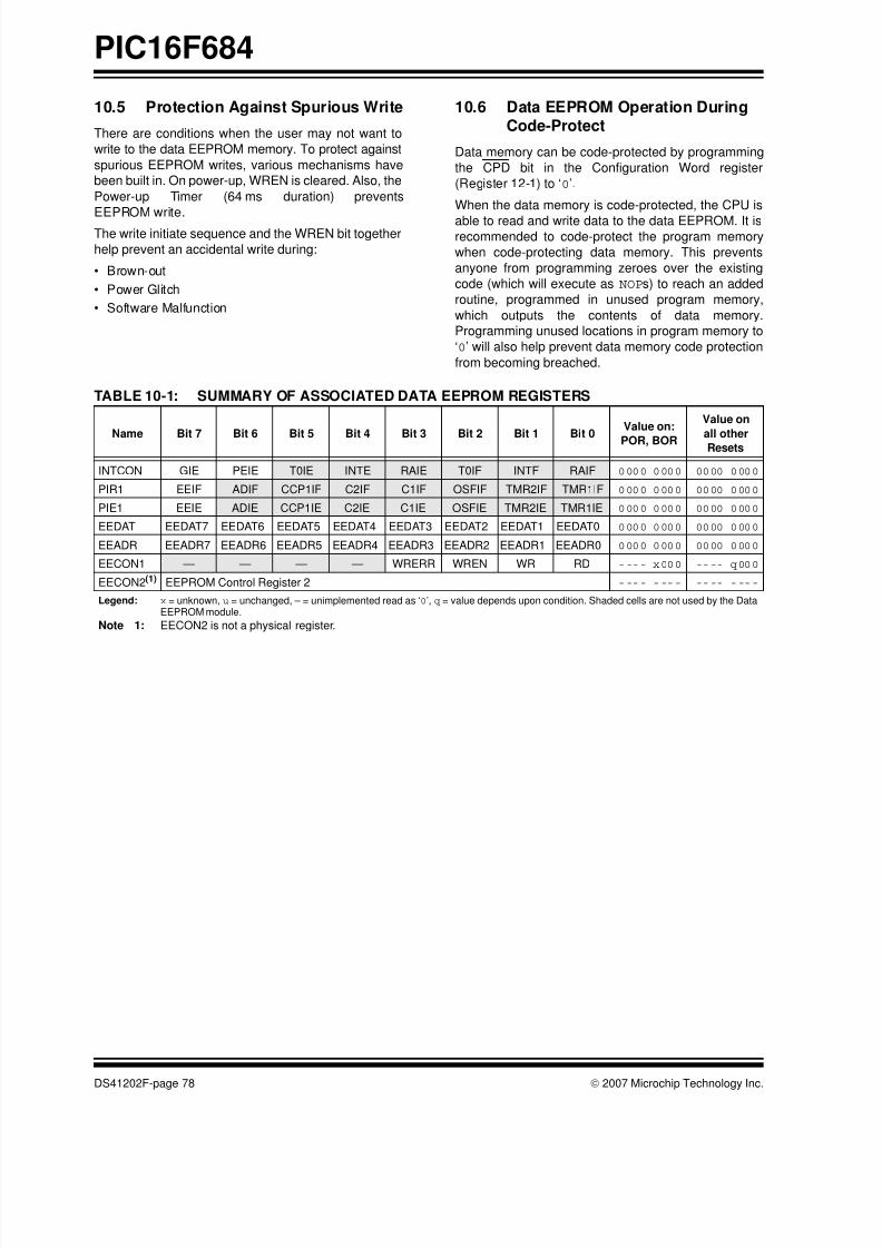
8/10/2019 PIC16F684 Datasheet
http://slidepdf.com/reader/full/pic16f684-datasheet 80/192
PIC16F684
DS41202F-page 78 © 2007 Microchip Technology Inc.
10.5 Protection Against Spurious Write
There are conditions when the user may not want to
write to the data EEPROM memory. To protect against
spurious EEPROM writes, various mechanisms have
been built in. On power-up, WREN is cleared. Also, the
Power-up Timer (64 ms duration) prevents
EEPROM write.The write initiate sequence and the WREN bit together
help prevent an accidental write during:
• Brown-out
• Power Glitch
• Software Malfunction
10.6 Data EEPROM Operation DuringCode-Protect
Data memory can be code-protected by programming
the CPD bit in the Configuration Word register
(Register 12-1) to ‘0’.
When the data memory is code-protected, the CPU is
able to read and write data to the data EEPROM. It isrecommended to code-protect the program memory
when code-protecting data memory. This prevents
anyone from programming zeroes over the existing
code (which will execute as NOPs) to reach an added
routine, programmed in unused program memory,
which outputs the contents of data memory.
Programming unused locations in program memory to
‘0’ will also help prevent data memory code protection
from becoming breached.
TABLE 10-1: SUMMARY OF ASSOCIATED DATA EEPROM REGISTERS
Name Bit 7 Bit 6 Bit 5 Bit 4 Bit 3 Bit 2 Bit 1 Bit 0
Value on:
POR, BOR
Value on
all otherResets
INTCON GIE PEIE T0IE INTE RAIE T0IF INTF RAIF 0000 0000 0000 0000
PIR1 EEIF ADIF CCP1IF C2IF C1IF OSFIF TMR2IF TMR1IF 0000 0000 0000 0000
PIE1 EEIE ADIE CCP1IE C2IE C1IE OSFIE TMR2IE TMR1IE 0000 0000 0000 0000
EEDAT EEDAT7 EEDAT6 EEDAT5 EEDAT4 EEDAT3 EEDAT2 EEDAT1 EEDAT0 0000 0000 0000 0000
EEADR EEADR7 EEADR6 EEADR5 EEADR4 EEADR3 EEADR2 EEADR1 EEADR0 0000 0000 0000 0000
EECON1 — — — — WRERR WREN WR RD ---- x000 ---- q000
EECON2(1) EEPROM Control Register 2 ---- ---- ---- ----
Legend: x = unknown, u = unchanged, – = unimplemented read as ‘0’, q = value depends upon condition. Shaded cells are not used by the DataEEPROM module.
Note 1: EECON2 is not a physical register.
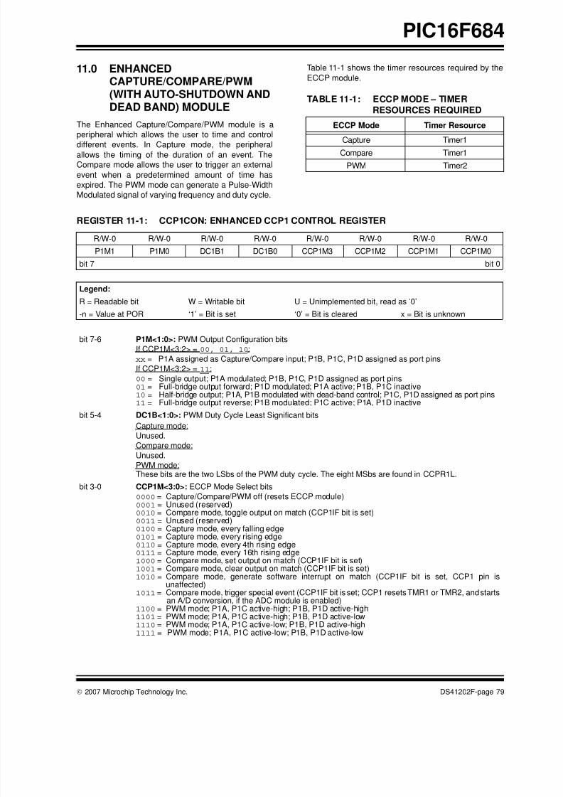
8/10/2019 PIC16F684 Datasheet
http://slidepdf.com/reader/full/pic16f684-datasheet 81/192
© 2007 Microchip Technology Inc. DS41202F-page 79
PIC16F684
11.0 ENHANCEDCAPTURE/COMPARE/PWM(WITH AUTO-SHUTDOWN ANDDEAD BAND) MODULE
The Enhanced Capture/Compare/PWM module is a
peripheral which allows the user to time and control
different events. In Capture mode, the peripheral
allows the timing of the duration of an event. The
Compare mode allows the user to trigger an external
event when a predetermined amount of time has
expired. The PWM mode can generate a Pulse-Width
Modulated signal of varying frequency and duty cycle.
Table 11-1 shows the timer resources required by the
ECCP module.
TABLE 11-1: ECCP MODE – TIMER
RESOURCES REQUIRED
ECCP Mode Timer Resource
Capture Timer1
Compare Timer1
PWM Timer2
REGISTER 11-1: CCP1CON: ENHANCED CCP1 CONTROL REGISTER
R/W-0 R/W-0 R/W-0 R/W-0 R/W-0 R/W-0 R/W-0 R/W-0
P1M1 P1M0 DC1B1 DC1B0 CCP1M3 CCP1M2 CCP1M1 CCP1M0
bit 7 bit 0
Legend:
R = Readable bit W = Writable bit U = Unimplemented bit, read as ‘0’
-n = Value at POR ‘1’ = Bit is set ‘0’ = Bit is cleared x = Bit is unknown
bit 7-6 P1M<1:0>: PWM Output Configuration bits
If CCP1M<3:2> = 00, 01, 10:
xx = P1A assigned as Capture/Compare input; P1B, P1C, P1D assigned as port pins
If CCP1M<3:2> = 11:
00 = Single output; P1A modulated; P1B, P1C, P1D assigned as port pins01 = Full-bridge output forward; P1D modulated; P1A active; P1B, P1C inactive10 = Half-bridge output; P1A, P1B modulated with dead-band control; P1C, P1D assigned as port pins11 = Full-bridge output reverse; P1B modulated; P1C active; P1A, P1D inactive
bit 5-4 DC1B<1:0>: PWM Duty Cycle Least Significant bitsCapture mode:
Unused.
Compare mode:
Unused.
PWM mode:These bits are the two LSbs of the PWM duty cycle. The eight MSbs are found in CCPR1L.
bit 3-0 CCP1M<3:0>: ECCP Mode Select bits
0000 = Capture/Compare/PWM off (resets ECCP module)0001 = Unused (reserved)0010 = Compare mode, toggle output on match (CCP1IF bit is set)0011 = Unused (reserved)0100 = Capture mode, every falling edge0101 = Capture mode, every rising edge0110 = Capture mode, every 4th rising edge0111 = Capture mode, every 16th rising edge1000 = Compare mode, set output on match (CCP1IF bit is set)1001 = Compare mode, clear output on match (CCP1IF bit is set)1010 = Compare mode, generate software interrupt on match (CCP1IF bit is set, CCP1 pin is
unaffected)1011 = Compare mode, trigger special event (CCP1IF bit is set; CCP1 resets TMR1 or TMR2, and starts
an A/D conversion, if the ADC module is enabled)1100 = PWM mode; P1A, P1C active-high; P1B, P1D active-high1101 = PWM mode; P1A, P1C active-high; P1B, P1D active-low1110 = PWM mode; P1A, P1C active-low; P1B, P1D active-high1111 = PWM mode; P1A, P1C active-low; P1B, P1D active-low
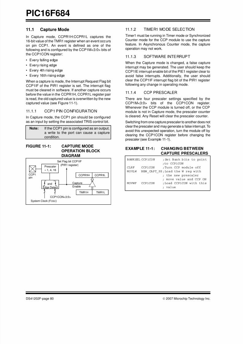
8/10/2019 PIC16F684 Datasheet
http://slidepdf.com/reader/full/pic16f684-datasheet 82/192
PIC16F684
DS41202F-page 80 © 2007 Microchip Technology Inc.
11.1 Capture Mode
In Capture mode, CCPR1H:CCPR1L captures the
16-bit value of the TMR1 register when an event occurs
on pin CCP1. An event is defined as one of the
following and is configured by the CCP1M<3:0> bits of
the CCP1CON register:
• Every falling edge• Every rising edge
• Every 4th rising edge
• Every 16th rising edge
When a capture is made, the Interrupt Request Flag bit
CCP1IF of the PIR1 register is set. The interrupt flag
must be cleared in software. If another capture occurs
before the value in the CCPR1H, CCPR1L register pair
is read, the old captured value is overwritten by the new
captured value (see Figure 11-1).
11.1.1 CCP1 PIN CONFIGURATION
In Capture mode, the CCP1 pin should be configured
as an input by setting the associated TRIS control bit.
FIGURE 11-1: CAPTURE MODEOPERATION BLOCK
DIAGRAM
11.1.2 TIMER1 MODE SELECTION
Timer1 must be running in Timer mode or Synchronized
Counter mode for the CCP module to use the capture
feature. In Asynchronous Counter mode, the capture
operation may not work.
11.1.3 SOFTWARE INTERRUPT
When the Capture mode is changed, a false capture
interrupt may be generated. The user should keep the
CCP1IE interrupt enable bit of the PIE1 register clear to
avoid false interrupts. Additionally, the user should
clear the CCP1IF interrupt flag bit of the PIR1 register
following any change in operating mode.
11.1.4 CCP PRESCALER
There are four prescaler settings specified by the
CCP1M<3:0> bits of the CCP1CON register.
Whenever the CCP module is turned off, or the CCP
module is not in Capture mode, the prescaler counter
is cleared. Any Reset will clear the prescaler counter.
Switching from one capture prescaler to another does not
clear the prescaler and may generate a false interrupt. To
avoid this unexpected operation, turn the module off by
clearing the CCP1CON register before changing the
prescaler (see Example 11-1).
EXAMPLE 11-1: CHANGING BETWEEN
CAPTURE PRESCALERS
Note: If the CCP1 pin is configured as an output,
a write to the port can cause a capture
condition.
CCPR1H CCPR1L
TMR1H TMR1L
Set Flag bit CCP1IF
(PIR1 register)
Capture
Enable
CCP1CON<3:0>
Prescaler
÷ 1, 4, 16
and
Edge Detect
pinCCP1
System Clock (FOSC)
BANKSEL CCP1CON ;Set Bank bits to point
;to CCP1CON
CLRF CCP1CON ;Turn CCP module off
MOVLW NEW_CAPT_PS;Load the W reg with
; the new prescaler
; move value and CCP ONMOVWF CCP1CON ;Load CCP1CON with this
; value
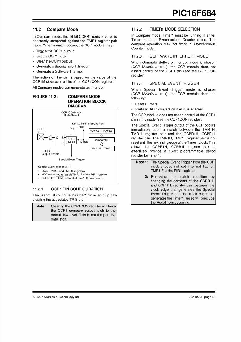
8/10/2019 PIC16F684 Datasheet
http://slidepdf.com/reader/full/pic16f684-datasheet 83/192
© 2007 Microchip Technology Inc. DS41202F-page 81
PIC16F684
11.2 Compare Mode
In Compare mode, the 16-bit CCPR1 register value is
constantly compared against the TMR1 register pair
value. When a match occurs, the CCP module may:
• Toggle the CCP1 output
• Set the CCP1 output
• Clear the CCP1 output
• Generate a Special Event Trigger
• Generate a Software Interrupt
The action on the pin is based on the value of the
CCP1M<3:0> control bits of the CCP1CON register.
All Compare modes can generate an interrupt.
FIGURE 11-2: COMPARE MODE
OPERATION BLOCKDIAGRAM
11.2.1 CCP1 PIN CONFIGURATION
The user must configure the CCP1 pin as an output by
clearing the associated TRIS bit.
11.2.2 TIMER1 MODE SELECTION
In Compare mode, Timer1 must be running in either
Timer mode or Synchronized Counter mode. The
compare operation may not work in Asynchronous
Counter mode.
11.2.3 SOFTWARE INTERRUPT MODE
When Generate Software Interrupt mode is chosen
(CCP1M<3:0> = 1010), the CCP module does not
assert control of the CCP1 pin (see the CCP1CON
register).
11.2.4 SPECIAL EVENT TRIGGER
When Special Event Trigger mode is chosen
(CCP1M<3:0> = 1011), the CCP module does the
following:
• Resets Timer1
• Starts an ADC conversion if ADC is enabled
The CCP module does not assert control of the CCP1
pin in this mode (see the CCP1CON register).The Special Event Trigger output of the CCP occurs
immediately upon a match between the TMR1H,
TMR1L register pair and the CCPR1H, CCPR1L
register pair. The TMR1H, TMR1L register pair is not
reset until the next rising edge of the Timer1 clock. This
allows the CCPR1H, CCPR1L register pair to
effectively provide a 16-bit programmable period
register for Timer1.
Note: Clearing the CCP1CON register will force
the CCP1 compare output latch to the
default low level. This is not the port I/O
data latch.
CCPR1H CCPR1L
TMR1H TMR1L
ComparatorQ S
R
OutputLogic
Special Event Trigger
Set CCP1IF Interrupt Flag(PIR1)
Match
TRIS
CCP1CON<3:0>Mode Select
Output Enable
Pin
Special Event Trigger will:
• Clear TMR1H and TMR1L registers.
• NOT set interrupt flag bit TMR1IF of the PIR1 register.
• Set the GO/DONE bit to start the ADC conversion.
CCP1 4
Note 1: The Special Event Trigger from the CCP
module does not set interrupt flag bit
TMR1IF of the PIR1 register.
2: Removing the match condition by
changing the contents of the CCPR1Hand CCPR1L register pair, between the
clock edge that generates the Special
Event Trigger and the clock edge that
generates the Timer1 Reset, will preclude
the Reset from occurring.
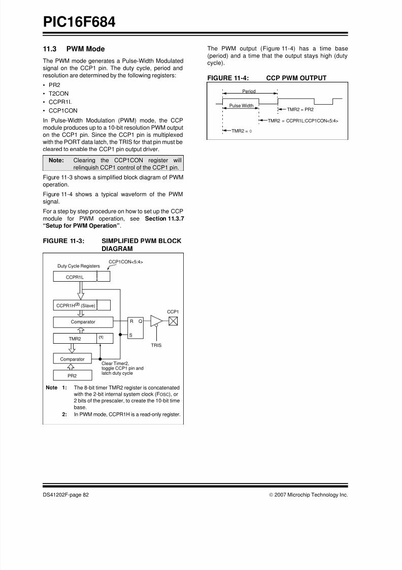
8/10/2019 PIC16F684 Datasheet
http://slidepdf.com/reader/full/pic16f684-datasheet 84/192
PIC16F684
DS41202F-page 82 © 2007 Microchip Technology Inc.
11.3 PWM Mode
The PWM mode generates a Pulse-Width Modulated
signal on the CCP1 pin. The duty cycle, period and
resolution are determined by the following registers:
• PR2
• T2CON
• CCPR1L
• CCP1CON
In Pulse-Width Modulation (PWM) mode, the CCP
module produces up to a 10-bit resolution PWM output
on the CCP1 pin. Since the CCP1 pin is multiplexed
with the PORT data latch, the TRIS for that pin must be
cleared to enable the CCP1 pin output driver.
Figure 11-3 shows a simplified block diagram of PWM
operation.
Figure 11-4 shows a typical waveform of the PWM
signal.
For a step by step procedure on how to set up the CCP
module for PWM operation, see Section 11.3.7
“Setup for PWM Operation”.
FIGURE 11-3: SIMPLIFIED PWM BLOCKDIAGRAM
The PWM output (Figure 11-4) has a time base
(period) and a time that the output stays high (duty
cycle).
FIGURE 11-4: CCP PWM OUTPUT
Note: Clearing the CCP1CON register will
relinquish CCP1 control of the CCP1 pin.
CCPR1L
CCPR1H(2) (Slave)
Comparator
TMR2
PR2
(1)
R Q
S
Duty Cycle RegistersCCP1CON<5:4>
Clear Timer2,toggle CCP1 pin andlatch duty cycle
Note 1: The 8-bit timer TMR2 register is concatenated
with the 2-bit internal system clock (FOSC), or
2 bits of the prescaler, to create the 10-bit timebase.
2: In PWM mode, CCPR1H is a read-only register.
TRIS
CCP1
Comparator
Period
Pulse Width
TMR2 = 0
TMR2 = CCPR1L:CCP1CON<5:4>
TMR2 = PR2
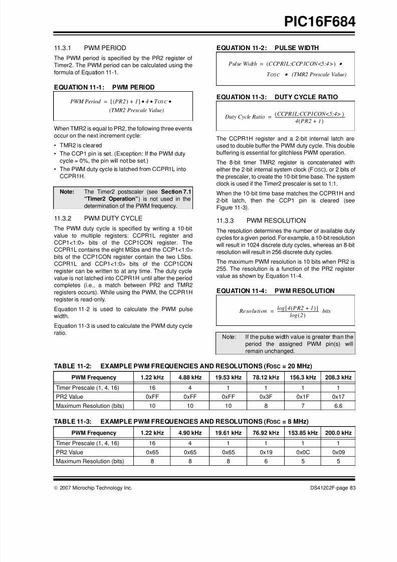
8/10/2019 PIC16F684 Datasheet
http://slidepdf.com/reader/full/pic16f684-datasheet 85/192
© 2007 Microchip Technology Inc. DS41202F-page 83
PIC16F684
11.3.1 PWM PERIOD
The PWM period is specified by the PR2 register of
Timer2. The PWM period can be calculated using the
formula of Equation 11-1.
EQUATION 11-1: PWM PERIOD
When TMR2 is equal to PR2, the following three events
occur on the next increment cycle:
• TMR2 is cleared
• The CCP1 pin is set. (Exception: If the PWM duty
cycle = 0%, the pin will not be set.)
• The PWM duty cycle is latched from CCPR1L into
CCPR1H.
11.3.2 PWM DUTY CYCLE
The PWM duty cycle is specified by writing a 10-bit
value to multiple registers: CCPR1L register and
CCP1<1:0> bits of the CCP1CON register. The
CCPR1L contains the eight MSbs and the CCP1<1:0>
bits of the CCP1CON register contain the two LSbs.
CCPR1L and CCP1<1:0> bits of the CCP1CON
register can be written to at any time. The duty cycle
value is not latched into CCPR1H until after the period
completes (i.e., a match between PR2 and TMR2
registers occurs). While using the PWM, the CCPR1Hregister is read-only.
Equation 11-2 is used to calculate the PWM pulse
width.
Equation 11-3 is used to calculate the PWM duty cycle
ratio.
EQUATION 11-2: PULSE WIDTH
EQUATION 11-3: DUTY CYCLE RATIO
The CCPR1H register and a 2-bit internal latch are
used to double buffer the PWM duty cycle. This double
buffering is essential for glitchless PWM operation.
The 8-bit timer TMR2 register is concatenated with
either the 2-bit internal system clock (FOSC), or 2 bits of
the prescaler, to create the 10-bit time base. The system
clock is used if the Timer2 prescaler is set to 1:1.
When the 10-bit time base matches the CCPR1H and
2-bit latch, then the CCP1 pin is cleared (see
Figure 11-3).
11.3.3 PWM RESOLUTION
The resolution determines the number of available duty
cycles for a given period. For example, a 10-bit resolution
will result in 1024 discrete duty cycles, whereas an 8-bit
resolution will result in 256 discrete duty cycles.
The maximum PWM resolution is 10 bits when PR2 is
255. The resolution is a function of the PR2 register
value as shown by Equation 11-4.
EQUATION 11-4: PWM RESOLUTION
TABLE 11-2: EXAMPLE PWM FREQUENCIES AND RESOLUTIONS (FOSC = 20 MHz)
TABLE 11-3: EXAMPLE PWM FREQUENCIES AND RESOLUTIONS (FOSC = 8 MHz)
Note: The Timer2 postscaler (see Section 7.1
“Timer2 Operation”) is not used in thedetermination of the PWM frequency.
PWM Period PR2( ) 1+[ ] 4 T OS C •••=
(TMR2 Prescale Value)
Note: If the pulse width value is greater than the
period the assigned PWM pin(s) will
remain unchanged.
Pulse Width CCPR1L:CCP1CON<5:4>( ) • =
T OS C • (TMR2 Prescale Value)
Duty Cycle RatioCCPR1L:CCP1CON<5:4>( )
4 PR2 1+( )-----------------------------------------------------------------------=
Reso lu tion4 PR2 1+( )[ ]log
2( )log------------------------------------------ bits=
PWM Frequency 1.22 kHz 4.88 kHz 19.53 kHz 78.12 kHz 156.3 kHz 208.3 kHz
Timer Prescale (1, 4, 16) 16 4 1 1 1 1
PR2 Value 0xFF 0xFF 0xFF 0x3F 0x1F 0x17
Maximum Resolution (bits) 10 10 10 8 7 6.6
PWM Frequency 1.22 kHz 4.90 kHz 19.61 kHz 76.92 kHz 153.85 kHz 200.0 kHz
Timer Prescale (1, 4, 16) 16 4 1 1 1 1
PR2 Value 0x65 0x65 0x65 0x19 0x0C 0x09
Maximum Resolution (bits) 8 8 8 6 5 5
8/10/2019 PIC16F684 Datasheet
http://slidepdf.com/reader/full/pic16f684-datasheet 86/192
PIC16F684
DS41202F-page 84 © 2007 Microchip Technology Inc.
11.3.4 OPERATION IN SLEEP MODE
In Sleep mode, the TMR2 register will not increment
and the state of the module will not change. If the CCP1
pin is driving a value, it will continue to drive that value.
When the device wakes up, TMR2 will continue from its
previous state.
11.3.5 CHANGES IN SYSTEM CLOCKFREQUENCY
The PWM frequency is derived from the system clock
frequency. Any changes in the system clock frequency
will result in changes to the PWM frequency. See
Section 3.0 “Oscillator Module (With Fail-Safe
Clock Monitor)” for additional details.
11.3.6 EFFECTS OF RESET
Any Reset will force all ports to Input mode and the
CCP registers to their Reset states.
11.3.7 SETUP FOR PWM OPERATION
The following steps should be taken when configuring
the CCP module for PWM operation:
1. Disable the PWM pin (CCP1) output driver by
setting the associated TRIS bit.
2. Set the PWM period by loading the PR2 register.
3. Configure the CCP module for the PWM modeby loading the CCP1CON register with the
appropriate values.
4. Set the PWM duty cycle by loading the CCPR1L
register and CCP1 bits of the CCP1CON register.
5. Configure and start Timer2:
• Clear the TMR2IF interrupt flag bit of the
PIR1 register.
• Set the Timer2 prescale value by loading the
T2CKPS bits of the T2CON register.
• Enable Timer2 by setting the TMR2ON bit of
the T2CON register.
6. Enable PWM output after a new PWM cycle has
started:
• Wait until Timer2 overflows (TMR2IF bit of
the PIR1 register is set).
• Enable the CCP1 pin output driver by clearing
the associated TRIS bit.
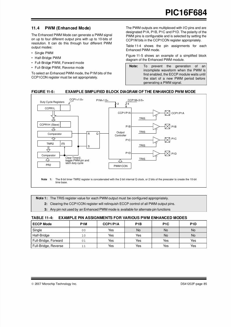
8/10/2019 PIC16F684 Datasheet
http://slidepdf.com/reader/full/pic16f684-datasheet 87/192
© 2007 Microchip Technology Inc. DS41202F-page 85
PIC16F684
11.4 PWM (Enhanced Mode)
The Enhanced PWM Mode can generate a PWM signal
on up to four different output pins with up to 10-bits of
resolution. It can do this through four different PWM
output modes:
• Single PWM
• Half-Bridge PWM
• Full-Bridge PWM, Forward mode
• Full-Bridge PWM, Reverse mode
To select an Enhanced PWM mode, the P1M bits of the
CCP1CON register must be set appropriately.
The PWM outputs are multiplexed with I/O pins and are
designated P1A, P1B, P1C and P1D. The polarity of the
PWM pins is configurable and is selected by setting the
CCP1M bits in the CCP1CON register appropriately.
Table 11-4 shows the pin assignments for each
Enhanced PWM mode.
Figure 11-5 shows an example of a simplified blockdiagram of the Enhanced PWM module.
FIGURE 11-5: EXAMPLE SIMPLIFIED BLOCK DIAGRAM OF THE ENHANCED PWM MODE
TABLE 11-4: EXAMPLE PIN ASSIGNMENTS FOR VARIOUS PWM ENHANCED MODES
Note: To prevent the generation of an
incomplete waveform when the PWM is
first enabled, the ECCP module waits until
the start of a new PWM period before
generating a PWM signal.
CCPR1L
CCPR1H (Slave)
Comparator
TMR2
Comparator
PR2
(1)
R Q
S
Duty Cycle RegistersCCP1<1:0>
Clear Timer2,toggle PWM pin andlatch duty cycle
Note 1: The 8-bit timer TMR2 register is concatenated with the 2-bit internal Q clock, or 2 bits of the prescaler to create the 10-bittime base.
TRISCCP1/P1A
TRIS
P1B
TRIS
P1C
TRIS
P1D
OutputController
P1M<1:0>
2
CCP1M<3:0>
4
PWM1CON
CCP1/P1A
P1B
P1C
P1D
Note 1: The TRIS register value for each PWM output must be configured appropriately.
2: Clearing the CCP1CON register will relinquish ECCP control of all PWM output pins.
3: Any pin not used by an Enhanced PWM mode is available for alternate pin functions
ECCP Mode P1M CCP1/P1A P1B P1C P1D
Single 00 Yes No No No
Half-Bridge 10 Yes Yes No No
Full-Bridge, Forward 01 Yes Yes Yes Yes
Full-Bridge, Reverse 11 Yes Yes Yes Yes
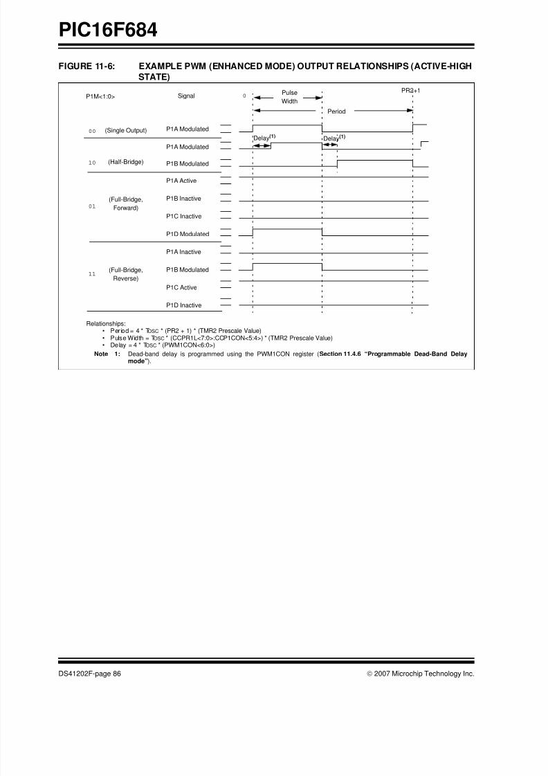
8/10/2019 PIC16F684 Datasheet
http://slidepdf.com/reader/full/pic16f684-datasheet 88/192
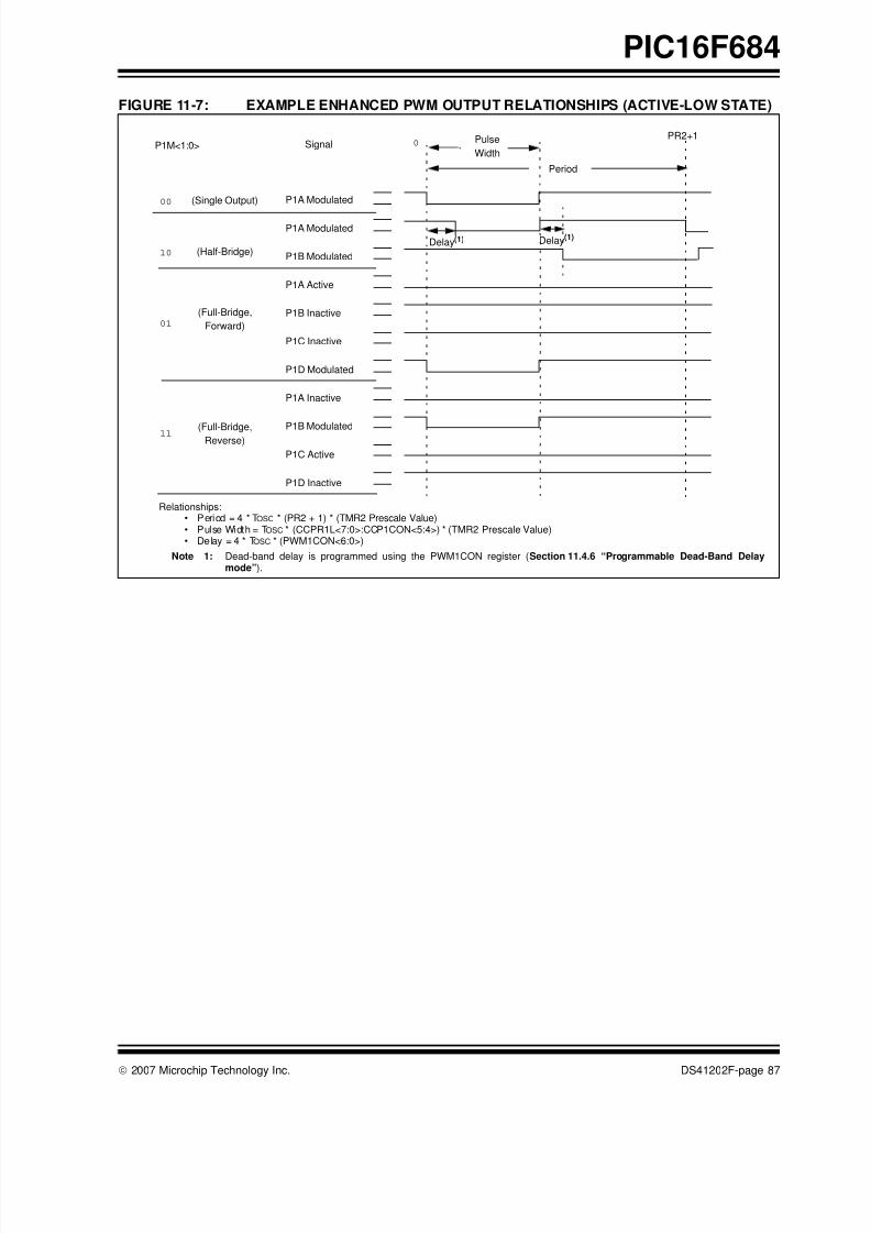
8/10/2019 PIC16F684 Datasheet
http://slidepdf.com/reader/full/pic16f684-datasheet 89/192
© 2007 Microchip Technology Inc. DS41202F-page 87
PIC16F684
FIGURE 11-7: EXAMPLE ENHANCED PWM OUTPUT RELATIONSHIPS (ACTIVE-LOW STATE)
0
Period
00
10
01
11
SignalPR2+1
P1M<1:0>
P1A Modulated
P1A Modulated
P1B Modulated
P1A Active
P1B Inactive
P1C Inactive
P1D Modulated
P1A Inactive
P1B Modulated
P1C Active
P1D Inactive
Pulse
Width
(Single Output)
(Half-Bridge)
(Full-Bridge,
Forward)
(Full-Bridge,Reverse)
Delay(1) Delay(1)
Relationships:• Period = 4 * TOSC * (PR2 + 1) * (TMR2 Prescale Value)• Pulse Width = TOSC * (CCPR1L<7:0>:CCP1CON<5:4>) * (TMR2 Prescale Value)• Delay = 4 * TOSC * (PWM1CON<6:0>)
Note 1: Dead-band delay is programmed using the PWM1CON register (Section 11.4.6 “Programmable Dead-Band Delaymode”).
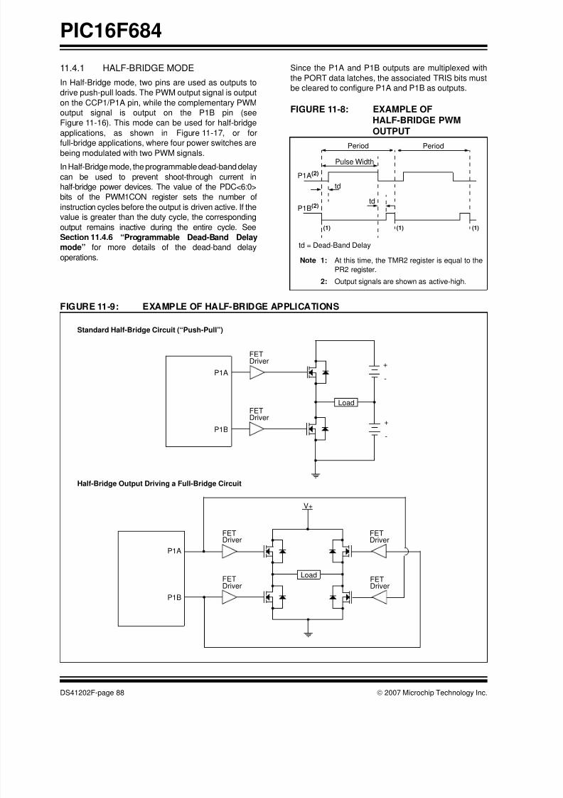
8/10/2019 PIC16F684 Datasheet
http://slidepdf.com/reader/full/pic16f684-datasheet 90/192
PIC16F684
DS41202F-page 88 © 2007 Microchip Technology Inc.
11.4.1 HALF-BRIDGE MODE
In Half-Bridge mode, two pins are used as outputs to
drive push-pull loads. The PWM output signal is output
on the CCP1/P1A pin, while the complementary PWM
output signal is output on the P1B pin (see
Figure 11-16). This mode can be used for half-bridge
applications, as shown in Figure 11-17, or for
full-bridge applications, where four power switches are
being modulated with two PWM signals.
In Half-Bridge mode, the programmable dead-band delay
can be used to prevent shoot-through current in
half-bridge power devices. The value of the PDC<6:0>
bits of the PWM1CON register sets the number of
instruction cycles before the output is driven active. If the
value is greater than the duty cycle, the corresponding
output remains inactive during the entire cycle. See
Section 11.4.6 “Programmable Dead-Band Delay
mode” for more details of the dead-band delay
operations.
Since the P1A and P1B outputs are multiplexed with
the PORT data latches, the associated TRIS bits must
be cleared to configure P1A and P1B as outputs.
FIGURE 11-8: EXAMPLE OFHALF-BRIDGE PWM
OUTPUT
FIGURE 11-9: EXAMPLE OF HALF-BRIDGE APPLICATIONS
Period
Pulse Width
td
td
(1)
P1A(2)
P1B(2)
td = Dead-Band Delay
Period
(1) (1)
Note 1: At this time, the TMR2 register is equal to the
PR2 register.
2: Output signals are shown as active-high.
P1A
P1B
FETDriver
FET
Driver
Load
+
-
+
-
FETDriver
FETDriver
V+
Load
FETDriver
FETDriver
P1A
P1B
Standard Half-Bridge Circuit (“Push-Pull”)
Half-Bridge Output Driving a Full-Bridge Circuit
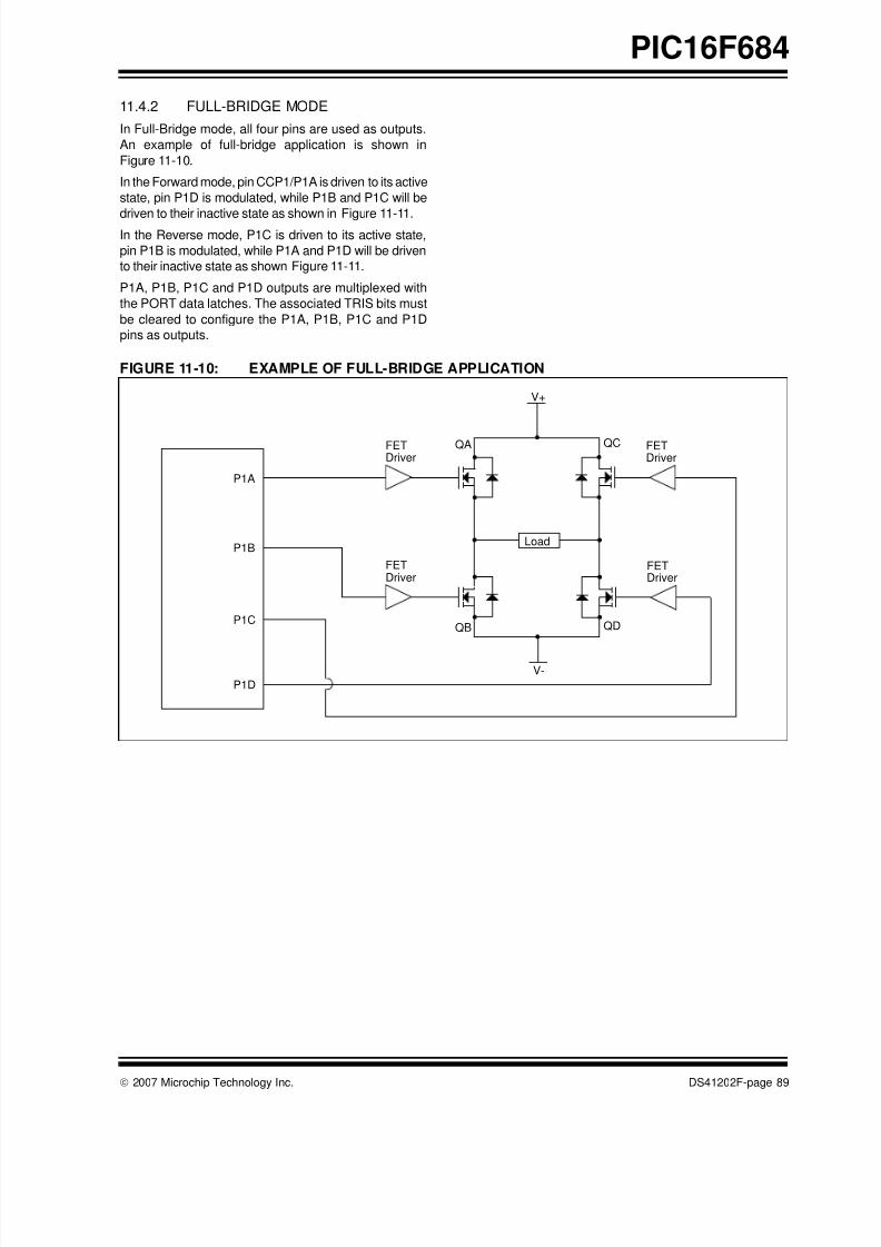
8/10/2019 PIC16F684 Datasheet
http://slidepdf.com/reader/full/pic16f684-datasheet 91/192
© 2007 Microchip Technology Inc. DS41202F-page 89
PIC16F684
11.4.2 FULL-BRIDGE MODE
In Full-Bridge mode, all four pins are used as outputs.
An example of full-bridge application is shown in
Figure 11-10.
In the Forward mode, pin CCP1/P1A is driven to its active
state, pin P1D is modulated, while P1B and P1C will be
driven to their inactive state as shown in Figure 11-11.In the Reverse mode, P1C is driven to its active state,
pin P1B is modulated, while P1A and P1D will be driven
to their inactive state as shown Figure 11-11.
P1A, P1B, P1C and P1D outputs are multiplexed with
the PORT data latches. The associated TRIS bits must
be cleared to configure the P1A, P1B, P1C and P1D
pins as outputs.
FIGURE 11-10: EXAMPLE OF FULL-BRIDGE APPLICATION
P1A
P1C
FETDriver
FETDriver
V+
V-
Load
FETDriver
FETDriver
P1B
P1D
QA
QB QD
QC
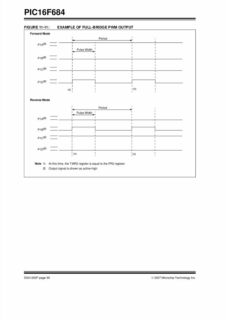
8/10/2019 PIC16F684 Datasheet
http://slidepdf.com/reader/full/pic16f684-datasheet 92/192
PIC16F684
DS41202F-page 90 © 2007 Microchip Technology Inc.
FIGURE 11-11: EXAMPLE OF FULL-BRIDGE PWM OUTPUT
Period
Pulse Width
P1A(2)
P1B(2)
P1C(2)
P1D(2)
Forward Mode
(1)
Period
Pulse Width
P1A(2)
P1C(2)
P1D(2)
P1B(2)
Reverse Mode
(1)
(1)(1)
Note 1: At this time, the TMR2 register is equal to the PR2 register.
2: Output signal is shown as active-high.
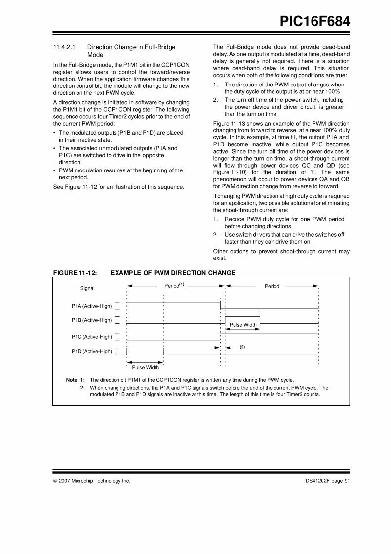
8/10/2019 PIC16F684 Datasheet
http://slidepdf.com/reader/full/pic16f684-datasheet 93/192
© 2007 Microchip Technology Inc. DS41202F-page 91
PIC16F684
11.4.2.1 Direction Change in Full-Bridge
Mode
In the Full-Bridge mode, the P1M1 bit in the CCP1CON
register allows users to control the forward/reverse
direction. When the application firmware changes this
direction control bit, the module will change to the new
direction on the next PWM cycle.
A direction change is initiated in software by changing
the P1M1 bit of the CCP1CON register. The following
sequence occurs four Timer2 cycles prior to the end of
the current PWM period:
• The modulated outputs (P1B and P1D) are placed
in their inactive state.
• The associated unmodulated outputs (P1A and
P1C) are switched to drive in the opposite
direction.
• PWM modulation resumes at the beginning of the
next period.
See Figure 11-12 for an illustration of this sequence.
The Full-Bridge mode does not provide dead-band
delay. As one output is modulated at a time, dead-band
delay is generally not required. There is a situation
where dead-band delay is required. This situation
occurs when both of the following conditions are true:
1. The direction of the PWM output changes when
the duty cycle of the output is at or near 100%.
2. The turn off time of the power switch, including
the power device and driver circuit, is greater
than the turn on time.
Figure 11-13 shows an example of the PWM direction
changing from forward to reverse, at a near 100% duty
cycle. In this example, at time t1, the output P1A and
P1D become inactive, while output P1C becomes
active. Since the turn off time of the power devices is
longer than the turn on time, a shoot-through current
will flow through power devices QC and QD (see
Figure 11-10) for the duration of ‘t’. The same
phenomenon will occur to power devices QA and QB
for PWM direction change from reverse to forward.
If changing PWM direction at high duty cycle is requiredfor an application, two possible solutions for eliminating
the shoot-through current are:
1. Reduce PWM duty cycle for one PWM period
before changing directions.
2. Use switch drivers that can drive the switches off
faster than they can drive them on.
Other options to prevent shoot-through current may
exist.
FIGURE 11-12: EXAMPLE OF PWM DIRECTION CHANGE
Pulse Width
Period(1)Signal
Note 1: The direction bit P1M1 of the CCP1CON register is written any time during the PWM cycle.
2: When changing directions, the P1A and P1C signals switch before the end of the current PWM cycle. Themodulated P1B and P1D signals are inactive at this time. The length of this time is four Timer2 counts.
Period
(2)
P1A (Active-High)
P1B (Active-High)
P1C (Active-High)
P1D (Active-High)
Pulse Width
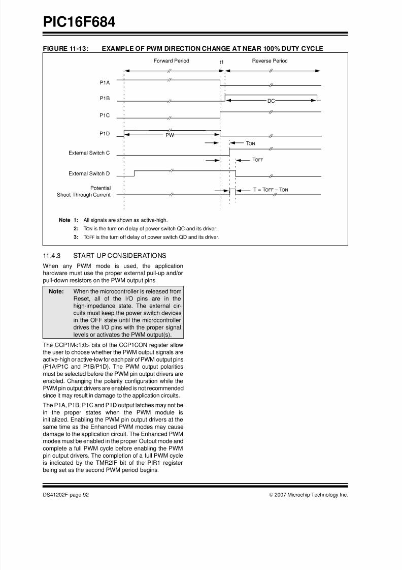
8/10/2019 PIC16F684 Datasheet
http://slidepdf.com/reader/full/pic16f684-datasheet 94/192
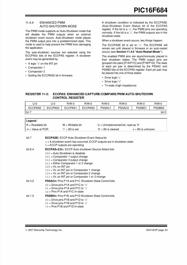
8/10/2019 PIC16F684 Datasheet
http://slidepdf.com/reader/full/pic16f684-datasheet 95/192
© 2007 Microchip Technology Inc. DS41202F-page 93
PIC16F684
11.4.4 ENHANCED PWM
AUTO-SHUTDOWN MODE
The PWM mode supports an Auto-Shutdown mode that
will disable the PWM outputs when an external
shutdown event occurs. Auto-Shutdown mode places
the PWM output pins into a predetermined state. This
mode is used to help prevent the PWM from damaging
the application.
The auto-shutdown sources are selected using the
ECCPASx bits of the ECCPAS register. A shutdown
event may be generated by:
• A logic ‘0’ on the INT pin
• Comparator 1
• Comparator 2
• Setting the ECCPASE bit in firmware
A shutdown condition is indicated by the ECCPASE
(Auto-Shutdown Event Status) bit of the ECCPAS
register. If the bit is a ‘0’, the PWM pins are operating
normally. If the bit is a ‘1’, the PWM outputs are in the
shutdown state.
When a shutdown event occurs, two things happen:
The ECCPASE bit is set to ‘1’. The ECCPASE willremain set until cleared in firmware or an auto-restart
occurs (see Section 11.4.5 “Auto-Restart Mode”).
The enabled PWM pins are asynchronously placed in
their shutdown states. The PWM output pins are
grouped into pairs [P1A/P1C] and [P1B/P1D]. The state
of each pin pair is determined by the PSSAC and
PSSBD bits of the ECCPAS register. Each pin pair may
be placed into one of three states:
• Drive logic ‘1’
• Drive logic ‘0’
• Tri-state (high-impedance)
REGISTER 11-2: ECCPAS: ENHANCED CAPTURE/COMPARE/PWM AUTO-SHUTDOWNCONTROL REGISTER
U-0 U-0 R/W-0 R/W-0 R/W-0 R/W-0 R/W-0 R/W-0
ECCPASE ECCPAS2 ECCPAS1 ECCPAS0 PSSAC1 PSSAC0 PSSBD1 PSSBD0
bit 7 bit 0
Legend:
R = Readable bit W = Writable bit U = Unimplemented bit, read as ‘0’
-n = Value at POR ‘1’ = Bit is set ‘0’ = Bit is cleared x = Bit is unknown
bit 7 ECCPASE: ECCP Auto-Shutdown Event Status bit
1 = A shutdown event has occurred; ECCP outputs are in shutdown state
0 = ECCP outputs are operating
bit 6-4 ECCPAS<2:0>: ECCP Auto-shutdown Source Select bits
000 = Auto-Shutdown is disabled
001 = Comparator 1 output change
010 = Comparator 2 output change
011 = Either Comparator 1 or 2 change
100 = VIL on INT pin
101 = VIL on INT pin or Comparator 1 change
110 = VIL on INT pin or Comparator 2 change
111 = VIL on INT pin or Comparator 1 or 2 change
bit 3-2 PSSACn: Pins P1A and P1C Shutdown State Control bits
00 = Drive pins P1A and P1C to ‘0’01 = Drive pins P1A and P1C to ‘1’
1x = Pins P1A and P1C tri-state
bit 1-0 PSSBDn: Pins P1B and P1D Shutdown State Control bits
00 = Drive pins P1B and P1D to ‘0’
01 = Drive pins P1B and P1D to ‘1’
1x = Pins P1B and P1D tri-state
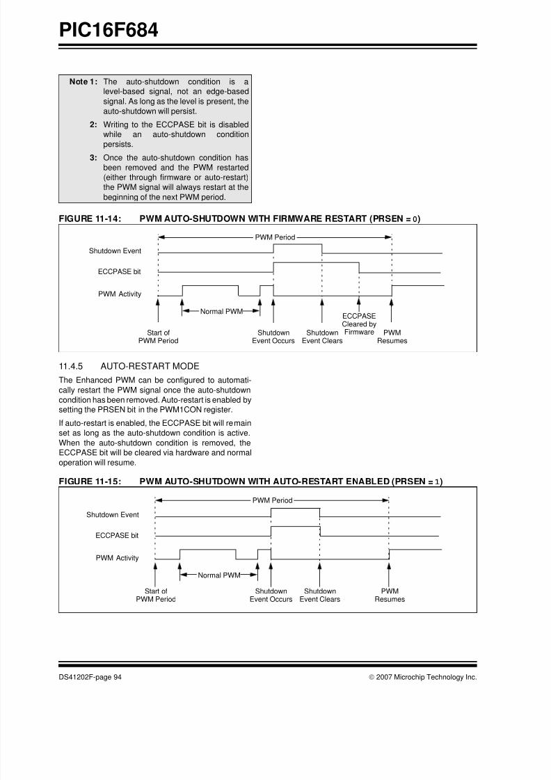
8/10/2019 PIC16F684 Datasheet
http://slidepdf.com/reader/full/pic16f684-datasheet 96/192
PIC16F684
DS41202F-page 94 © 2007 Microchip Technology Inc.
FIGURE 11-14: PWM AUTO-SHUTDOWN WITH FIRMWARE RESTART (PRSEN = 0)
11.4.5 AUTO-RESTART MODE
The Enhanced PWM can be configured to automati-
cally restart the PWM signal once the auto-shutdown
condition has been removed. Auto-restart is enabled by
setting the PRSEN bit in the PWM1CON register.
If auto-restart is enabled, the ECCPASE bit will remain
set as long as the auto-shutdown condition is active.
When the auto-shutdown condition is removed, the
ECCPASE bit will be cleared via hardware and normal
operation will resume.
FIGURE 11-15: PWM AUTO-SHUTDOWN WITH AUTO-RESTART ENABLED (PRSEN = 1)
Note 1: The auto-shutdown condition is a
level-based signal, not an edge-based
signal. As long as the level is present, the
auto-shutdown will persist.
2: Writing to the ECCPASE bit is disabled
while an auto-shutdown conditionpersists.
3: Once the auto-shutdown condition has
been removed and the PWM restarted
(either through firmware or auto-restart)
the PWM signal will always restart at the
beginning of the next PWM period.
Shutdown
PWM
ECCPASE bit
Activity
Event
ShutdownEvent Occurs
ShutdownEvent Clears
PWMResumes
Normal PWM
Start ofPWM Period
ECCPASECleared byFirmware
PWM Period
Shutdown
PWM
ECCPASE bit
Activity
Event
ShutdownEvent Occurs
ShutdownEvent Clears
PWMResumes
Normal PWM
Start ofPWM Period
PWM Period

8/10/2019 PIC16F684 Datasheet
http://slidepdf.com/reader/full/pic16f684-datasheet 97/192
© 2007 Microchip Technology Inc. DS41202F-page 95
PIC16F684
11.4.6 PROGRAMMABLE DEAD-BAND
DELAY MODE
In half-bridge applications where all power switches are
modulated at the PWM frequency, the power switches
normally require more time to turn off than to turn on. If
both the upper and lower power switches are switched
at the same time (one turned on, and the other turned
off), both switches may be on for a short period of time
until one switch completely turns off. During this brief
interval, a very high current (shoot-through current ) will
flow through both power switches, shorting the bridge
supply. To avoid this potentially destructive
shoot-through current from flowing during switching,
turning on either of the power switches is normally
delayed to allow the other switch to completely turn off.
In Half-Bridge mode, a digitally programmable
dead-band delay is available to avoid shoot-through
current from destroying the bridge power switches. The
delay occurs at the signal transition from the non-active
state to the active state. See Section FIGURE 11-17:
“Example of Half-Bridge Applications” forillustration. The lower seven bits of the associated
PWM1CON register (Register 11-3) sets the delay
period in terms of microcontroller instruction cycles
(TCY or 4 TOSC).
FIGURE 11-16: EXAMPLE OF
HALF-BRIDGE PWMOUTPUT
FIGURE 11-17: EXAMPLE OF HALF-BRIDGE APPLICATIONS
Period
Pulse Width
td
td
(1)
P1A(2)
P1B(2)
td = Dead-Band Delay
Period
(1) (1)
Note 1: At this time, the TMR2 register is equal to the
PR2 register.
2: Output signals are shown as active-high.
P1A
P1B
FETDriver
FETDriver
V+
V-
Load
+V-
+V-
Standard Half-Bridge Circuit (“Push-Pull”)

8/10/2019 PIC16F684 Datasheet
http://slidepdf.com/reader/full/pic16f684-datasheet 98/192
PIC16F684
DS41202F-page 96 © 2007 Microchip Technology Inc.
TABLE 11-5: SUMMARY OF REGISTERS ASSOCIATED WITH CAPTURE, COMPARE AND PWM
REGISTER 11-3: PWM1CON: ENHANCED PWM CONTROL REGISTER
R/W-0 R/W-0 R/W-0 R/W-0 R/W-0 R/W-0 R/W-0 R/W-0
PRSEN PDC6 PDC5 PDC4 PDC3 PDC2 PDC1 PDC0
bit 7 bit 0
Legend:
R = Readable bit W = Writable bit U = Unimplemented bit, read as ‘0’
-n = Value at POR ‘1’ = Bit is set ‘0’ = Bit is cleared x = Bit is unknown
bit 7 PRSEN: PWM Restart Enable bit
1 = Upon auto-shutdown, the ECCPASE bit clears automatically once the shutdown event goes
away; the PWM restarts automatically
0 = Upon auto-shutdown, ECCPASE must be cleared in software to restart the PWM
bit 6-0 PDC<6:0>: PWM Delay Count bits
PDCn = Number of FOSC /4 (4 * TOSC) cycles between the scheduled time when a PWM signal
should transition active and the actual time it transitions active
Note 1: Bit resets to ‘0’ with Two-Speed Start-up and LP, XT or HS selected as the Oscillator mode or Fail-Safe
mode is enabled.
Name Bit 7 Bit 6 Bit 5 Bit 4 Bit 3 Bit 2 Bit 1 Bit 0Value on:
POR, BOR
Value on
all other
Resets
CCPR1L Capture/Compare/PWM Register 1 Low Byte xxxx xxxx uuuu uuuu
CCPR1H Capture/Compare/PWM Register 1 High Byte xxxx xxxx uuuu uuuu
CCP1CON P1M1 P1M0 DC1B1 DC1B0 CCP1M3 CCP1M2 CCP1M1 CCP1M0 0000 0000 0000 0000
CMCON0 C2OUT C1OUT C2INV C1INV CIS CM2 CM1 CM0 0000 0000 0000 0000
CMCON1 — — — — — — T1GSS C2SYNC ---- --10 ---- --10
ECCPAS ECCPASE ECCPAS2 ECCPAS1 ECCPAS0 PSSAC1 PSSAC0 PSSBD1 PSSBD0 0000 0000 0000 0000
INTCON GIE PEIE T0IE INTE RAIE T0IF INTF RAIF 0000 0000 0000 0000
PIE1 EEIE ADIE CCP1IE C2IE C1IE OSFIE TMR2IE TMR1IE 0000 0000 0000 0000
PIR1 EEIF ADIF CCP1IF C2IF C1IF OSFIF TMR2IF TMR1IF 0000 0000 0000 0000
PR2 Timer2 Module Period Register 1111 1111 1111 1111
PWM1CON PRSEN PDC6 PDC5 PDC4 PDC3 PDC2 PDC1 PDC0 0000 0000 0000 0000
T1CON T1GINV TMR1GE T1CKPS1 T1CKPS0 T1OSCEN T1SYNC TMR1CS TMR1ON 0000 0000 uuuu uuuu
T2CON — TOUTPS3 TOUTPS2 TOUTPS1 TOUTPS0 TMR2ON T2CKPS1 T2CKPS0 -000 0000 -000 0000
TMR1L Holding Register for the Least Significant Byte of the 16-bit TMR1 Register xxxx xxxx uuuu uuuu
TMR1H Holding Register for the Most Significant Byte of the 16-bit TMR1 Register xxxx xxxx uuuu uuuu
TMR2 Timer2 Module Register 0000 0000 0000 0000
TRISA — — TRISA5 TRISA4 TRISA3 TRISA2 TRISA1 TRISA0 --11 1111 --11 1111TRISC — — TRISC5 TRISC4 TRISC3 TRISC2 TRISC1 TRISC0 --11 1111 --11 1111
Legend: - = Unimplemented locations, read as ‘0’, u = unchanged, x = unknown. Shaded cells are not used by the Capture,
Compare and PWM.
8/10/2019 PIC16F684 Datasheet
http://slidepdf.com/reader/full/pic16f684-datasheet 99/192

8/10/2019 PIC16F684 Datasheet
http://slidepdf.com/reader/full/pic16f684-datasheet 100/192
PIC16F684
DS41202F-page 98 © 2007 Microchip Technology Inc.
REGISTER 12-1: CONFIG: CONFIGURATION WORD REGISTER
— — — — FCMEN IESO BOREN1 BOREN0
bit 15 bit 8
CPD CP MCLRE PWRTE WDTE FOSC2 FOSC1 FOSC0
bit 7 bit 0
Legend:
R = Readable bit W = Writable bit P = Programmable’ U = Unimplemented bit, read as ‘0’
-n = Value at POR ‘1’ = Bit is set ‘0’ = Bit is cleared x = Bit is unknown
bit 15-12 Unimplemented: Read as ‘1’
bit 11 FCMEN: Fail-Safe Clock Monitor Enabled bit
1 = Fail-Safe Clock Monitor is enabled
0 = Fail-Safe Clock Monitor is disabled
bit 10 IESO: Internal External Switchover bit1 = Internal External Switchover mode is enabled
0 = Internal External Switchover mode is disabled
bit 9-8 BOREN<1:0>: Brown-out Reset Selection bits(1)
11 = BOR enabled
10 = BOR enabled during operation and disabled in Sleep
01 = BOR controlled by SBOREN bit of the PCON register
00 = BOR disabled
bit 7 CPD: Data Code Protection bit(2)
1 = Data memory code protection is disabled
0 = Data memory code protection is enabled
bit 6 CP: Code Protection bit(3)
1 = Program memory code protection is disabled
0 = Program memory code protection is enabled
bit 5 MCLRE: RA3/MCLR pin function select bit(4)
1 = RA3/MCLR pin function is MCLR
0 = RA3/MCLR pin function is digital input, MCLR internally tied to VDD
bit 4 PWRTE: Power-up Timer Enable bit
1 = PWRT disabled
0 = PWRT enabled
bit 3 WDTE: Watchdog Timer Enable bit
1 = WDT enabled
0 = WDT disabled and can be enabled by SWDTEN bit of the WDTCON register
bit 2-0 FOSC<2:0>: Oscillator Selection bits
111 = RC oscillator: CLKOUT function on RA4/OSC2/CLKOUT pin, RC on RA5/OSC1/CLKIN
110 = RCIO oscillator: I/O function on RA4/OSC2/CLKOUT pin, RC on RA5/OSC1/CLKIN
101 = INTOSC oscillator: CLKOUT function on RA4/OSC2/CLKOUT pin, I/O function on RA5/OSC1/CLKIN
100 = INTOSCIO oscillator: I/O function on RA4/OSC2/CLKOUT pin, I/O function on RA5/OSC1/CLKIN
011 = EC: I/O function on RA4/OSC2/CLKOUT pin, CLKIN on RA5/OSC1/CLKIN
010 = HS oscillator: High-speed crystal/resonator on RA4/OSC2/CLKOUT and RA5/OSC1/CLKIN
001 = XT oscillator: Crystal/resonator on RA4/OSC2/CLKOUT and RA5/OSC1/CLKIN
000 = LP oscillator: Low-power crystal on RA4/OSC2/CLKOUT and RA5/OSC1/CLKIN
Note 1: Enabling Brown-out Reset does not automatically enable Power-up Timer.
2: The entire data EEPROM will be erased when the code protection is turned off.
3: The entire program memory will be erased when the code protection is turned off.
4: When MCLR is asserted in INTOSC or RC mode, the internal clock oscillator is d isabled.

8/10/2019 PIC16F684 Datasheet
http://slidepdf.com/reader/full/pic16f684-datasheet 101/192
© 2007 Microchip Technology Inc. DS41202F-page 99
PIC16F684
12.2 Calibration Bits
Brown-out Reset (BOR), Power-on Reset (POR) and
8 MHz internal oscillator (HFINTOSC) are factory cali-
brated. These calibration values are stored in fuses
located in the Calibration Word (2009h). The Calibra-
tion Word is not erased when using the specified bulk
erase sequence in the “PIC12F6XX/16F6XX Memory Programming Specification” (DS41244) and thus, does
not require reprogramming.
12.3 Reset
The PIC16F684 differentiates between various kinds of
Reset:
a) Power-on Reset (POR)
b) WDT Reset during normal operation
c) WDT Reset during Sleep
d) MCLR Reset during normal operation
e) MCLR Reset during Sleep
f) Brown-out Reset (BOR)
Some registers are not affected in any Reset condition;
their status is unknown on POR and unchanged in any
other Reset. Most other registers are reset to a “Reset
state” on:
• Power-on Reset
• MCLR Reset
• MCLR Reset during Sleep• WDT Reset
• Brown-out Reset (BOR)
WDT wake-up does not cause register resets in the
same manner as a WDT Reset since wake-up is
viewed as the resumption of normal operation. TO and
PD bits are set or cleared differently in different Reset
situations, as indicated in Table 12-2. Software can use
these bits to determine the nature of the Reset. See
Table 12-4 for a full description of Reset states of all
registers.
A simplified block diagram of the On-Chip Reset Circuit
is shown in Figure 12-1.
The MCLR Reset path has a noise filter to detect andignore small pulses. See Section 15.0 “Electrical
Specifications” for pulse-width specifications.
FIGURE 12-1: SIMPLIFIED BLOCK DIAGRAM OF ON-CHIP RESET CIRCUIT
S
R Q
ExternalReset
MCLR/VPP pin
VDD
OSC1/
WDTModule
VDD RiseDetect
OST/PWRT
LFINTOSC
WDT
Time-out
Power-on Reset
OST
10-bit Ripple Counter
PWRT
Chip_Reset
11-bit Ripple Counter
Reset
Enable OST
Enable PWRT
SLEEP
Brown-out(1)
Reset
SBORENBOREN
CLKI pin
Note 1: Refer to the Configuration Word register (Register 12-1).
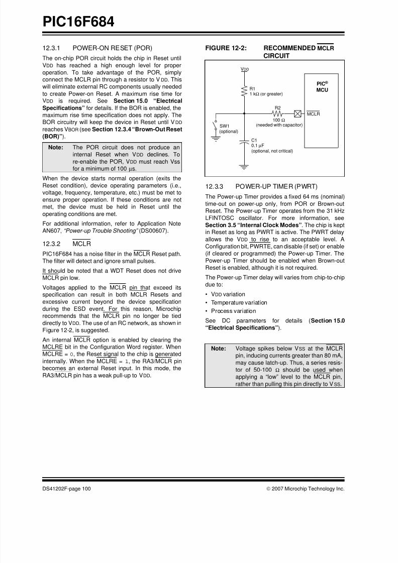
8/10/2019 PIC16F684 Datasheet
http://slidepdf.com/reader/full/pic16f684-datasheet 102/192
PIC16F684
DS41202F-page 100 © 2007 Microchip Technology Inc.
12.3.1 POWER-ON RESET (POR)
The on-chip POR circuit holds the chip in Reset until
VDD has reached a high enough level for proper
operation. To take advantage of the POR, simply
connect the MCLR pin through a resistor to VDD. This
will eliminate external RC components usually needed
to create Power-on Reset. A maximum rise time for
VDD is required. See Section 15.0 “Electrical
Specifications” for details. If the BOR is enabled, the
maximum rise time specification does not apply. The
BOR circuitry will keep the device in Reset until VDD
reaches VBOR (see Section 12.3.4 “Brown-Out Reset
(BOR)”).
When the device starts normal operation (exits the
Reset condition), device operating parameters (i.e.,
voltage, frequency, temperature, etc.) must be met to
ensure proper operation. If these conditions are not
met, the device must be held in Reset until the
operating conditions are met.
For additional information, refer to Application Note
AN607, “Power-up Trouble Shooting” (DS00607).
12.3.2 MCLR
PIC16F684 has a noise filter in the MCLR Reset path.
The filter will detect and ignore small pulses.
It should be noted that a WDT Reset does not drive
MCLR pin low.
Voltages applied to the MCLR pin that exceed its
specification can result in both MCLR Resets andexcessive current beyond the device specification
during the ESD event. For this reason, Microchip
recommends that the MCLR pin no longer be tied
directly to VDD. The use of an RC network, as shown in
Figure 12-2, is suggested.
An internal MCLR option is enabled by clearing the
MCLRE bit in the Configuration Word register. When
MCLRE = 0, the Reset signal to the chip is generated
internally. When the MCLRE = 1, the RA3/MCLR pin
becomes an external Reset input. In this mode, the
RA3/MCLR pin has a weak pull-up to VDD.
FIGURE 12-2: RECOMMENDED MCLR
CIRCUIT
12.3.3 POWER-UP TIMER (PWRT)
The Power-up Timer provides a fixed 64 ms (nominal)time-out on power-up only, from POR or Brown-out
Reset. The Power-up Timer operates from the 31 kHz
LFINTOSC oscillator. For more information, see
Section 3.5 “Internal Clock Modes”. The chip is kept
in Reset as long as PWRT is active. The PWRT delay
allows the VDD to rise to an acceptable level. A
Configuration bit, PWRTE, can disable (if set) or enable
(if cleared or programmed) the Power-up Timer. The
Power-up Timer should be enabled when Brown-out
Reset is enabled, although it is not required.
The Power-up Timer delay will varies from chip-to-chip
due to:
• VDD variation• Temperature variation
• Process variation
See DC parameters for details (Section 15.0
“Electrical Specifications”).
Note: The POR circuit does not produce an
internal Reset when VDD declines. To
re-enable the POR, VDD must reach Vss
for a minimum of 100 µs.
Note: Voltage spikes below VSS at the MCLR
pin, inducing currents greater than 80 mA,
may cause latch-up. Thus, a series resis-
tor of 50-100 Ω should be used when
applying a “low” level to the MCLR pin,
rather than pulling this pin directly to VSS.
VDD
PIC ®
MCLR
R11 kΩ (or greater)
C10.1 µF(optional, not critical)
R2
100 Ω(needed with capacitor)SW1
(optional)
MCU

8/10/2019 PIC16F684 Datasheet
http://slidepdf.com/reader/full/pic16f684-datasheet 103/192
© 2007 Microchip Technology Inc. DS41202F-page 101
PIC16F684
12.3.4 BROWN-OUT RESET (BOR)
The BOREN0 and BOREN1 bits in the Configuration
Word register select one of four BOR modes. Two
modes have been added to allow software or hardware
control of the BOR enable. When BOREN<1:0> = 01,
the SBOREN bit of the PCON register enables/disables
the BOR, allowing it to be controlled in software. By
selecting BOREN<1:0> = 10, the BOR is automatically
disabled in Sleep to conserve power and enabled on
wake-up. In this mode, the SBOREN bit is disabled.
See Register 12-1 for the Configuration Word
definition.
A brown-out occurs when VDD falls below VBOR for
greater than parameter TBOR (see Section 15.0
“Electrical Specifications”). The brown-out condition
will reset the device. This will occur regardless of VDD
slew rate. A Brown-out Reset may not occur if VDD falls
below VBOR for less than parameter TBOR.
On any Reset (Power-on, Brown-out Reset, Watchdog
Timer, etc.), the chip will remain in Reset until VDD rises
above VBOR (see Figure 12-3). If enabled, thePower-up Timer will be invoked by the Reset and keep
the chip in Reset an additional 64 ms.
If VDD drops below VBOR while the Power-up Timer is
running, the chip will go back into a Brown-out Reset
and the Power-up Timer will be re-initialized. Once VDD
rises above VBOR, the Power-up Timer will execute a
64 ms Reset.
12.3.5 BOR CALIBRATION
The PIC16F684 stores the BOR calibration values infuses located in the Calibration Word register (2008h).
The Calibration Word register is not erased when using
the specified bulk erase sequence in the
“PIC12F6XX/16F6XX Memory Programming Specifi-
cation ” (DS41204) and thus, does not require
reprogramming.
FIGURE 12-3: BROWN-OUT SITUATIONS
Note: The Power-up Timer is enabled by the
PWRTE bit in the Configuration Word
register.
Note: Address 2008h is beyond the user pro-
gram memory space. It belongs to the
special configuration memory space
(2000h-3FFFh), which can be accessed
only during programming. See
“PIC12F6XX/16F6XX Memory Program-
ming Specification” (DS41204) for moreinformation.
64 ms(1)
VBOR VDD
Internal
Reset
VBOR VDD
Internal
Reset 64 ms(1)< 64 ms
64 ms(1)
VBOR VDD
Internal
Reset
Note 1: 64 ms delay only if PWRTE bit is programmed to ‘0’.

8/10/2019 PIC16F684 Datasheet
http://slidepdf.com/reader/full/pic16f684-datasheet 104/192
PIC16F684
DS41202F-page 102 © 2007 Microchip Technology Inc.
12.3.6 TIME-OUT SEQUENCE
On power-up, the time-out sequence is as follows:
• PWRT time-out is invoked after POR has expired.
• OST is activated after the PWRT time-out has
expired.
The total time-out will vary based on oscillator
configuration and PWRTE bit status. For example, in ECmode with PWRTE bit erased (PWRT disabled), there
will be no time-out at all. Figure 12-4, Figure 12-5 and
Figure 12-6 depict time-out sequences. The device can
execute code from the INTOSC while OST is active by
enabling Two-Speed Start-up or Fail-Safe Monitor (see
Section 3.7.2 “Two-speed Start-up Sequence” and
Section 3.8 “Fail-Safe Clock Monitor”).
Since the time-outs occur from the POR pulse, if MCLR
is kept low long enough, the time-outs will expire. Then,
bringing MCLR high will begin execution immediately
(see Figure 12-5). This is useful for testing purposes or
to synchronize more than one PIC16F684 device
operating in parallel.Table 12-5 shows the Reset conditions for some
special registers, while Table 12-4 shows the Reset
conditions for all the registers.
12.3.7 POWER CONTROL (PCON)
REGISTER
The Power Control register PCON (address 8Eh) has
two Status bits to indicate what type of Reset occurred
last.
Bit 0 is BOR (Brown-out). BOR is unknown on
Power-on Reset. It must then be set by the user andchecked on subsequent Resets to see if BOR = 0,
indicating that a Brown-out has occurred. The BOR
Status bit is a “don’t care” and is not necessarily
predictable if the brown-out circuit is disabled
(BOREN<1:0> = 00 in the Configuration Word
register).
Bit 1 is POR (Power-on Reset). It is a ‘0’ on Power-on
Reset and unaffected otherwise. The user must write a
‘1’ to this bit following a Power-on Reset. On a subse-
quent Reset, if POR is ‘0’, it will indicate that a
Power-on Reset has occurred (i.e., VDD may have
gone too low).
For more information, see Section 4.2.4 “UltraLow-Power Wake-up” and Section 12.3.4
“Brown-Out Reset (BOR)”.
TABLE 12-1: TIME-OUT IN VARIOUS SITUATIONS
TABLE 12-2: STATUS/PCON BITS AND THEIR SIGNIFICANCE
TABLE 12-3: SUMMARY OF REGISTERS ASSOCIATED WITH BROWN-OUT RESET
Oscillator ConfigurationPower-up Brown-out Reset Wake-up from
SleepPWRTE = 0 PWRTE = 1 PWRTE = 0 PWRTE = 1
XT, HS, LP TPWRT + 1024 •
TOSC
1024 • TOSC TPWRT + 1024 •
TOSC
1024 • TOSC 1024 • TOSC
RC, EC, INTOSC TPWRT — TPWRT — —
POR BOR TO PD Condition
0 x 1 1 Power-on Reset
u 0 1 1 Brown-out Reset
u u 0 u WDT Reset
u u 0 0 WDT Wake-up
u u u u MCLR Reset during normal operation
u u 1 0 MCLR Reset during Sleep
Legend: u = unchanged, x = unknown
Name Bit 7 Bit 6 Bit 5 Bit 4 Bit 3 Bit 2 Bit 1 Bit 0Value on:
POR, BOR
Value on
all other
Resets(1)
PCON — — ULPWUE SBOREN — — POR BOR --01 --qq --0u --uu
STATUS IRP RP1 RP0 TO PD Z DC C 0001 1xxx 000q quuu
Legend: u = unchanged, x = unknown, – = unimplemented bit, reads as ‘0’, q = value depends on condition.
Shaded cells are not used by BOR.
Note 1: Other (non Power-up) Resets include MCLR Reset and Watchdog Timer Reset during normal operation.
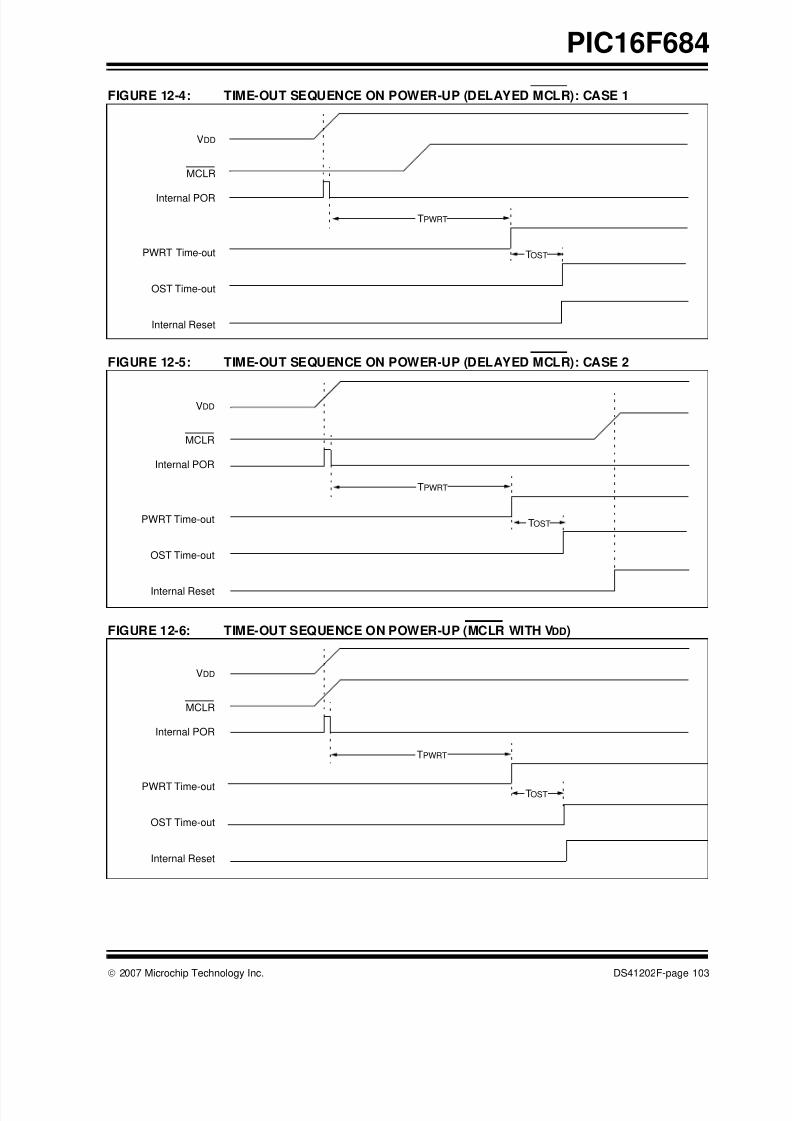
8/10/2019 PIC16F684 Datasheet
http://slidepdf.com/reader/full/pic16f684-datasheet 105/192
© 2007 Microchip Technology Inc. DS41202F-page 103
PIC16F684
FIGURE 12-4: TIME-OUT SEQUENCE ON POWER-UP (DELAYED MCLR): CASE 1
FIGURE 12-5: TIME-OUT SEQUENCE ON POWER-UP (DELAYED MCLR): CASE 2
FIGURE 12-6: TIME-OUT SEQUENCE ON POWER-UP (MCLR WITH VDD)
TPWRT
TOST
VDD
MCLR
Internal POR
PWRT Time-out
OST Time-out
Internal Reset
VDD
MCLR
Internal POR
PWRT Time-out
OST Time-out
Internal Reset
TPWRT
TOST
TOST
VDD
MCLR
Internal POR
PWRT Time-out
OST Time-out
Internal Reset
TPWRT

8/10/2019 PIC16F684 Datasheet
http://slidepdf.com/reader/full/pic16f684-datasheet 106/192
PIC16F684
DS41202F-page 104 © 2007 Microchip Technology Inc.
TABLE 12-4: INITIALIZATION CONDITION FOR REGISTERS
Register AddressPower-on
Reset
MCLR Reset
WDT Reset
Brown-out Reset(1)
Wake-up from Sleep through
Interrupt
Wake-up from Sleep through
WDT Time-out
W — xxxx xxxx uuuu uuuu uuuu uuuu
INDF 00h/80h xxxx xxxx xxxx xxxx uuuu uuuu
TMR0 01h xxxx xxxx uuuu uuuu uuuu uuuu
PCL 02h/82h 0000 0000 0000 0000 PC + 1(3)
STATUS 03h/83h 0001 1xxx 000q quuu(4) uuuq quuu(4)
FSR 04h/84h xxxx xxxx uuuu uuuu uuuu uuuu
PORTA(6) 05h --x0 x000 --u0 u000 --uu uuuu
PORTC(6) 07h --xx 0000 --uu 0000 --uu uuuu
PCLATH 0Ah/8Ah ---0 0000 ---0 0000 ---u uuuu
INTCON 0Bh/8Bh 0000 0000 0000 0000 uuuu uuuu(2)
PIR1 0Ch 0000 0000 0000 0000 uuuu uuuu(2)
TMR1L 0Eh xxxx xxxx uuuu uuuu uuuu uuuu
TMR1H 0Fh xxxx xxxx uuuu uuuu uuuu uuuu
T1CON 10h 0000 0000 uuuu uuuu -uuu uuuu
TMR2 11h 0000 0000 0000 0000 uuuu uuuu
T2CON 12h -000 0000 -000 0000 -uuu uuuu
CCPR1L 13h xxxx xxxx uuuu uuuu uuuu uuuu
CCPR1H 14h xxxx xxxx uuuu uuuu uuuu uuuu
CCP1CON 15h 0000 0000 0000 0000 uuuu uuuu
PWM1CON 16h 0000 0000 0000 0000 uuuu uuuu
ECCPAS 17h 0000 0000 0000 0000 uuuu uuuu
WDTCON 18h ---0 1000 ---0 1000 ---u uuuuCMCON0 19h 0000 0000 0000 0000 uuuu uuuu
CMCON1 1Ah ---- --10 ---- --10 ---- --uu
ADRESH 1Eh xxxx xxxx uuuu uuuu uuuu uuuu
ADCON0 1Fh 00-0 0000 00-0 0000 uu-u uuuu
OPTION_REG 81h 1111 1111 1111 1111 uuuu uuuu
TRISA 85h --11 1111 --11 1111 --uu uuuu
TRISC 87h --11 1111 --11 1111 --uu uuuu
PIE1 8Ch 0000 0000 0000 0000 uuuu uuuu
PCON 8Eh --01 --0x --0u --uq(1, 5) --uu --uu
OSCCON 8Fh -110 x000 -110 q000 -uuu uuuu
Legend: u = unchanged, x = unknown, – = unimplemented bit, reads as ‘0’, q = value depends on condition.Note 1: If VDD goes too low, Power-on Reset will be activated and registers will be affected differently.
2: One or more bits in INTCON and/or PIR1 will be affected (to cause wake-up).
3: When the wake-up is due to an interrupt and the GIE bit is set, the PC is loaded with the interrupt
vector (0004h).
4: See Table 12-5 for Reset value for specific condition.
5: If Reset was due to brown-out, then bit 0 = 0. All other Resets will cause bit 0 = u.
6: Port pins with analog functions controlled by the ANSEL register will read ‘0’ immediately after a Reset
even though the data latches are either undefined (POR) or unchanged (other Resets).
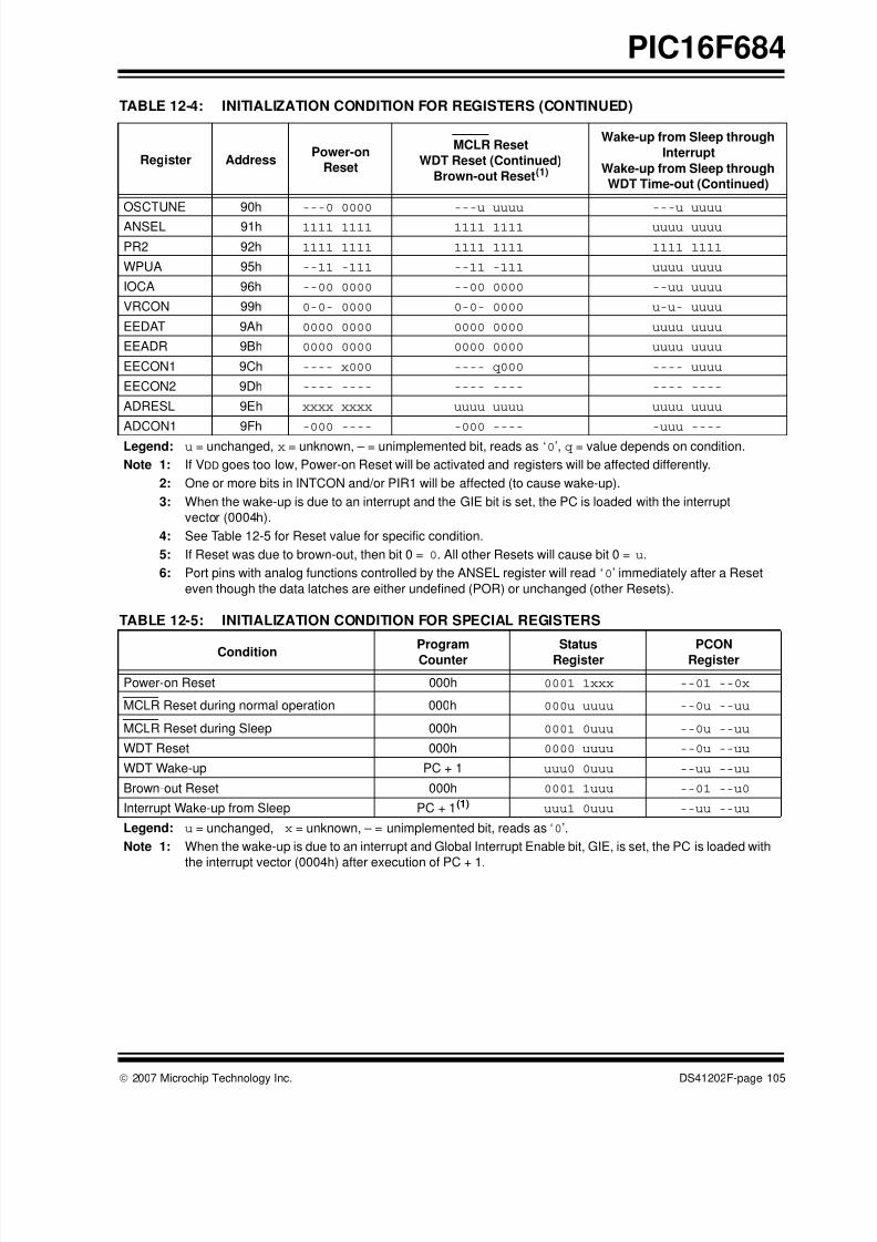
8/10/2019 PIC16F684 Datasheet
http://slidepdf.com/reader/full/pic16f684-datasheet 107/192
© 2007 Microchip Technology Inc. DS41202F-page 105
PIC16F684
TABLE 12-5: INITIALIZATION CONDITION FOR SPECIAL REGISTERS
OSCTUNE 90h ---0 0000 ---u uuuu ---u uuuu
ANSEL 91h 1111 1111 1111 1111 uuuu uuuu
PR2 92h 1111 1111 1111 1111 1111 1111
WPUA 95h --11 -111 --11 -111 uuuu uuuu
IOCA 96h --00 0000 --00 0000 --uu uuuu
VRCON 99h 0-0- 0000 0-0- 0000 u-u- uuuu
EEDAT 9Ah 0000 0000 0000 0000 uuuu uuuu
EEADR 9Bh 0000 0000 0000 0000 uuuu uuuu
EECON1 9Ch ---- x000 ---- q000 ---- uuuu
EECON2 9Dh ---- ---- ---- ---- ---- ----
ADRESL 9Eh xxxx xxxx uuuu uuuu uuuu uuuu
ADCON1 9Fh -000 ---- -000 ---- -uuu ----
ConditionProgram
Counter
Status
Register
PCON
Register
Power-on Reset 000h 0001 1xxx --01 --0x
MCLR Reset during normal operation 000h 000u uuuu --0u --uu
MCLR Reset during Sleep 000h 0001 0uuu --0u --uu
WDT Reset 000h 0000 uuuu --0u --uu
WDT Wake-up PC + 1 uuu0 0uuu --uu --uu
Brown-out Reset 000h 0001 1uuu --01 --u0
Interrupt Wake-up from Sleep PC + 1(1) uuu1 0uuu --uu --uu
Legend: u = unchanged, x = unknown, – = unimplemented bit, reads as ‘0’.
Note 1: When the wake-up is due to an interrupt and Global Interrupt Enable bit, GIE, is set, the PC is loaded with
the interrupt vector (0004h) after execution of PC + 1.
TABLE 12-4: INITIALIZATION CONDITION FOR REGISTERS (CONTINUED)
Register AddressPower-on
Reset
MCLR Reset
WDT Reset (Continued)
Brown-out Reset(1)
Wake-up from Sleep through
Interrupt
Wake-up from Sleep through
WDT Time-out (Continued)
Legend: u = unchanged, x = unknown, – = unimplemented bit, reads as ‘0’, q = value depends on condition.
Note 1: If VDD goes too low, Power-on Reset will be activated and registers will be affected differently.
2: One or more bits in INTCON and/or PIR1 will be affected (to cause wake-up).
3: When the wake-up is due to an interrupt and the GIE bit is set, the PC is loaded with the interrupt
vector (0004h).
4: See Table 12-5 for Reset value for specific condition.
5: If Reset was due to brown-out, then bit 0 = 0. All other Resets will cause bit 0 = u.
6: Port pins with analog functions controlled by the ANSEL register will read ‘0’ immediately after a Reset
even though the data latches are either undefined (POR) or unchanged (other Resets).
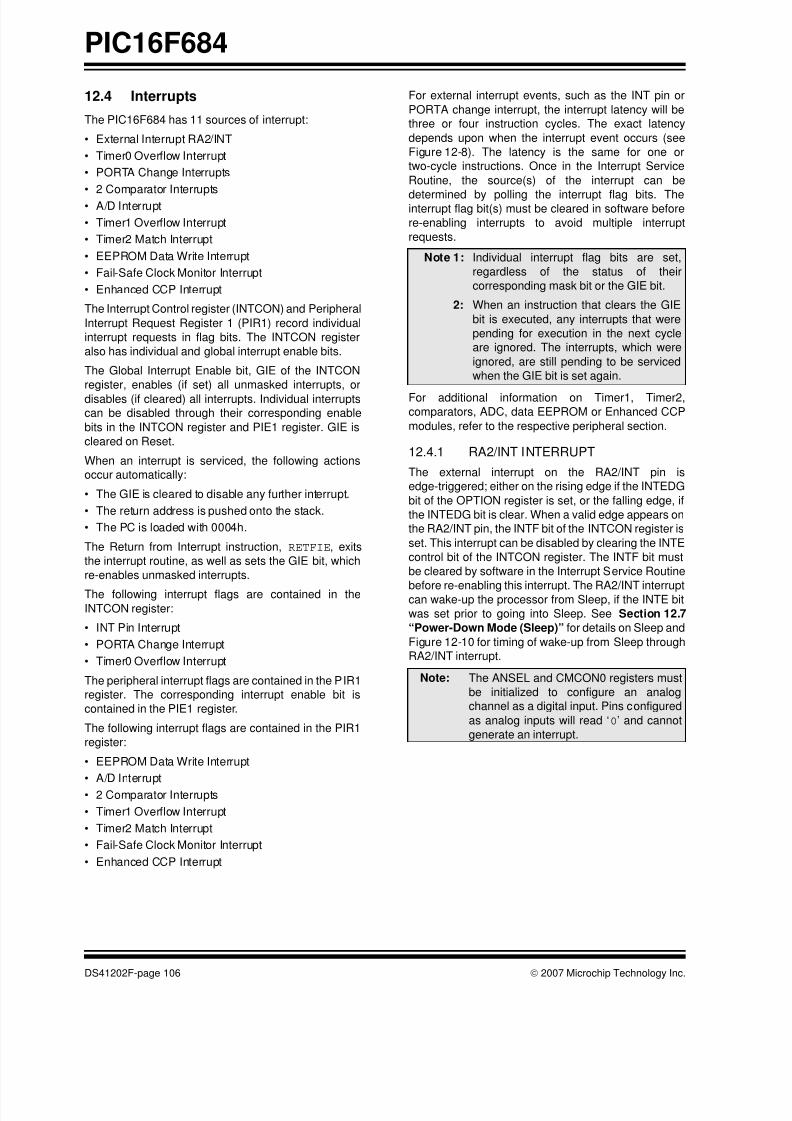
8/10/2019 PIC16F684 Datasheet
http://slidepdf.com/reader/full/pic16f684-datasheet 108/192
PIC16F684
DS41202F-page 106 © 2007 Microchip Technology Inc.
12.4 Interrupts
The PIC16F684 has 11 sources of interrupt:
• External Interrupt RA2/INT
• Timer0 Overflow Interrupt
• PORTA Change Interrupts
• 2 Comparator Interrupts
• A/D Interrupt
• Timer1 Overflow Interrupt
• Timer2 Match Interrupt
• EEPROM Data Write Interrupt
• Fail-Safe Clock Monitor Interrupt
• Enhanced CCP Interrupt
The Interrupt Control register (INTCON) and Peripheral
Interrupt Request Register 1 (PIR1) record individual
interrupt requests in flag bits. The INTCON register
also has individual and global interrupt enable bits.
The Global Interrupt Enable bit, GIE of the INTCON
register, enables (if set) all unmasked interrupts, or
disables (if cleared) all interrupts. Individual interrupts
can be disabled through their corresponding enable
bits in the INTCON register and PIE1 register. GIE is
cleared on Reset.
When an interrupt is serviced, the following actions
occur automatically:
• The GIE is cleared to disable any further interrupt.
• The return address is pushed onto the stack.
• The PC is loaded with 0004h.
The Return from Interrupt instruction, RETFIE, exits
the interrupt routine, as well as sets the GIE bit, which
re-enables unmasked interrupts.
The following interrupt flags are contained in the
INTCON register:
• INT Pin Interrupt
• PORTA Change Interrupt
• Timer0 Overflow Interrupt
The peripheral interrupt flags are contained in the PIR1
register. The corresponding interrupt enable bit is
contained in the PIE1 register.
The following interrupt flags are contained in the PIR1
register:
• EEPROM Data Write Interrupt
• A/D Interrupt
• 2 Comparator Interrupts
• Timer1 Overflow Interrupt
• Timer2 Match Interrupt
• Fail-Safe Clock Monitor Interrupt
• Enhanced CCP Interrupt
For external interrupt events, such as the INT pin or
PORTA change interrupt, the interrupt latency will be
three or four instruction cycles. The exact latency
depends upon when the interrupt event occurs (see
Figure 12-8). The latency is the same for one or
two-cycle instructions. Once in the Interrupt Service
Routine, the source(s) of the interrupt can be
determined by polling the interrupt flag bits. Theinterrupt flag bit(s) must be cleared in software before
re-enabling interrupts to avoid multiple interrupt
requests.
For additional information on Timer1, Timer2,
comparators, ADC, data EEPROM or Enhanced CCP
modules, refer to the respective peripheral section.
12.4.1 RA2/INT INTERRUPT
The external interrupt on the RA2/INT pin is
edge-triggered; either on the rising edge if the INTEDG
bit of the OPTION register is set, or the falling edge, if
the INTEDG bit is clear. When a valid edge appears on
the RA2/INT pin, the INTF bit of the INTCON register is
set. This interrupt can be disabled by clearing the INTE
control bit of the INTCON register. The INTF bit must
be cleared by software in the Interrupt Service Routine
before re-enabling this interrupt. The RA2/INT interruptcan wake-up the processor from Sleep, if the INTE bit
was set prior to going into Sleep. See Section 12.7
“Power-Down Mode (Sleep)” for details on Sleep and
Figure 12-10 for timing of wake-up from Sleep through
RA2/INT interrupt.
Note 1: Individual interrupt flag bits are set,
regardless of the status of their
corresponding mask bit or the GIE bit.
2: When an instruction that clears the GIE
bit is executed, any interrupts that were
pending for execution in the next cycle
are ignored. The interrupts, which were
ignored, are still pending to be serviced
when the GIE bit is set again.
Note: The ANSEL and CMCON0 registers must
be initialized to configure an analog
channel as a digital input. Pins configured
as analog inputs will read ‘0’ and cannot
generate an interrupt.
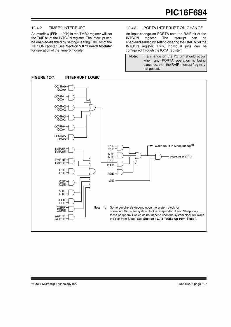
8/10/2019 PIC16F684 Datasheet
http://slidepdf.com/reader/full/pic16f684-datasheet 109/192
© 2007 Microchip Technology Inc. DS41202F-page 107
PIC16F684
12.4.2 TIMER0 INTERRUPT
An overflow (FFh → 00h) in the TMR0 register will set
the T0IF bit of the INTCON register. The interrupt can
be enabled/disabled by setting/clearing T0IE bit of the
INTCON register. See Section 5.0 “Timer0 Module”
for operation of the Timer0 module.
12.4.3 PORTA INTERRUPT-ON-CHANGE
An input change on PORTA sets the RAIF bit of the
INTCON register. The interrupt can be
enabled/disabled by setting/clearing the RAIE bit of the
INTCON register. Plus, individual pins can be
configured through the IOCA register.
FIGURE 12-7: INTERRUPT LOGIC
Note: If a change on the I/O pin should occurwhen any PORTA operation is being
executed, then the RAIF interrupt flag may
not get set.
TMR1IFTMR1IE
C1IFC1IE
T0IFT0IE
INTFINTE
RAIF
RAIE
GIE
PEIE
Wake-up (If in Sleep mode)(1)
Interrupt to CPU
EEIEEEIF
ADIFADIE
IOC-RA0IOCA0
IOC-RA1IOCA1
IOC-RA2IOCA2
IOC-RA3IOCA3
IOC-RA4IOCA4
IOC-RA5IOCA5
TMR2IFTMR2IE
CCP1IFCCP1IE
OSFIFOSFIE
C2IFC2IE
Note 1: Some peripherals depend upon the system clock for
operation. Since the system clock is suspended during Sleep, only
those peripherals which do not depend upon the system clock will wake
the part from Sleep. See Section 12.7.1 “Wake-up from Sleep”.
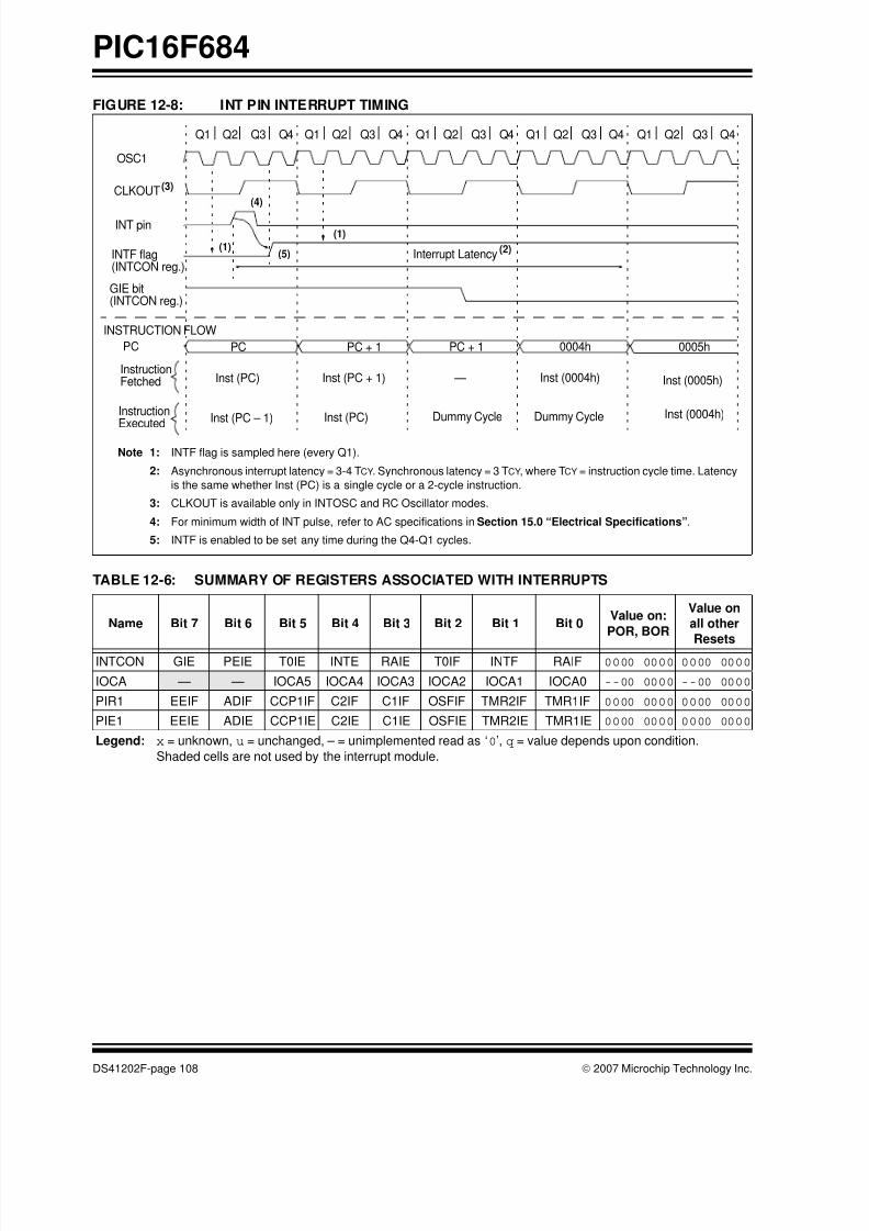
8/10/2019 PIC16F684 Datasheet
http://slidepdf.com/reader/full/pic16f684-datasheet 110/192
PIC16F684
DS41202F-page 108 © 2007 Microchip Technology Inc.
FIGURE 12-8: INT PIN INTERRUPT TIMING
TABLE 12-6: SUMMARY OF REGISTERS ASSOCIATED WITH INTERRUPTS
Name Bit 7 Bit 6 Bit 5 Bit 4 Bit 3 Bit 2 Bit 1 Bit 0Value on:
POR, BOR
Value on
all other
Resets
INTCON GIE PEIE T0IE INTE RAIE T0IF INTF RAIF 0000 0000 0000 0000
IOCA — — IOCA5 IOCA4 IOCA3 IOCA2 IOCA1 IOCA0 --00 0000 --00 0000
PIR1 EEIF ADIF CCP1IF C2IF C1IF OSFIF TMR2IF TMR1IF 0000 0000 0000 0000
PIE1 EEIE ADIE CCP1IE C2IE C1IE OSFIE TMR2IE TMR1IE 0000 0000 0000 0000
Legend: x = unknown, u = unchanged, – = unimplemented read as ‘0’, q = value depends upon condition.
Shaded cells are not used by the interrupt module.
Q2Q1 Q3 Q4 Q2Q1 Q3 Q4 Q2Q1 Q3 Q4 Q2Q1 Q3 Q4 Q2Q1 Q3 Q4
OSC1
CLKOUT
INT pin
INTF flag(INTCON reg.)
GIE bit(INTCON reg.)
INSTRUCTION FLOW
PC
InstructionFetched
InstructionExecuted
Interrupt Latency
PC PC + 1 PC + 1 0004h 0005h
Inst (0004h) Inst (0005h)
Dummy Cycle
Inst (PC) Inst (PC + 1)
Inst (PC – 1) Inst (0004h)Dummy CycleInst (PC)
—
Note 1: INTF flag is sampled here (every Q1).
2: Asynchronous interrupt latency = 3-4 TCY. Synchronous latency = 3 TCY, where TCY = instruction cycle time. Latency
is the same whether Inst (PC) is a single cycle or a 2-cycle instruction.
3: CLKOUT is available only in INTOSC and RC Oscillator modes.
4: For minimum width of INT pulse, refer to AC specifications in Section 15.0 “Electrical Specifications”.
5: INTF is enabled to be set any time during the Q4-Q1 cycles.
(1)
(2)
(3)
(4)
(5)(1)

8/10/2019 PIC16F684 Datasheet
http://slidepdf.com/reader/full/pic16f684-datasheet 111/192
© 2007 Microchip Technology Inc. DS41202F-page 109
PIC16F684
12.5 Context Saving During Interrupts
During an interrupt, only the return PC value is saved
on the stack. Typically, users may wish to save key
registers during an interrupt (e.g., W and STATUS
registers). This must be implemented in software.
Temporary holding registers W_TEMP and
STATUS_TEMP should be placed in the last 16 bytesof GPR (see Figure 2-2). These 16 locations are
common to all banks and do not require banking. This
makes context save and restore operations simpler.
The code shown in Example 12-1 can be used to:
• Store the W register
• Store the STATUS register
• Execute the ISR code
• Restore the Status (and Bank Select Bit register)
• Restore the W register
EXAMPLE 12-1: SAVING STATUS AND W REGISTERS IN RAM
Note: The PIC16F684 does not require saving
the PCLATH. However, if computed
GOTOs are used in both the ISR and the
main code, the PCLATH must be saved
and restored in the ISR.
MOVWF W_TEMP ;Copy W to TEMP register
SWAPF STATUS,W ;Swap status to be saved into W
;Swaps are used because they do not affect the status bits
MOVWF STATUS_TEMP ;Save status to bank zero STATUS_TEMP register
:
:(ISR) ;Insert user code here
:
SWAPF STATUS_TEMP,W ;Swap STATUS_TEMP register into W
;(sets bank to original state)MOVWF STATUS ;Move W into STATUS register
SWAPF W_TEMP,F ;Swap W_TEMP
SWAPF W_TEMP,W ;Swap W_TEMP into W

8/10/2019 PIC16F684 Datasheet
http://slidepdf.com/reader/full/pic16f684-datasheet 112/192
PIC16F684
DS41202F-page 110 © 2007 Microchip Technology Inc.
12.6 Watchdog Timer (WDT)
The WDT has the following features:
• Operates from the LFINTOSC (31 kHz)
• Contains a 16-bit prescaler
• Shares an 8-bit prescaler with Timer0
• Time-out period is from 1 ms to 268 seconds
• Configuration bit and software controlled
WDT is cleared under certain conditions described in
Table 12-7.
12.6.1 WDT OSCILLATOR
The WDT derives its time base from the 31 kHz
LFINTOSC. The LTS bit of the OSCCON register does
not reflect that the LFINTOSC is enabled.
The value of WDTCON is ‘---0 1000’ on all Resets.
This gives a nominal time base of 17 ms.
12.6.2 WDT CONTROL
The WDTE bit is located in the Configuration Word
register. When set, the WDT runs continuously.
When the WDTE bit in the Configuration Word register
is set, the SWDTEN bit of the WDTCON register has no
effect. If WDTE is clear, then the SWDTEN bit can be
used to enable and disable the WDT. Setting the bit willenable it and clearing the bit will disable it.
The PSA and PS<2:0> bits of the OPTION register
have the same function as in previous versions of the
PIC16F684 Family of microcontrollers. See
Section 5.0 “Timer0 Module” for more information.
FIGURE 12-9: WATCHDOG TIMER BLOCK DIAGRAM
Note: When the Oscillator Start-up Timer (OST)
is invoked, the WDT is held in Reset,
because the WDT Ripple Counter is used
by the OST to perform the oscillator delay
count. When the OST count has expired,
the WDT will begin counting (if enabled).
TABLE 12-7: WDT STATUS
Conditions WDT
WDTE = 0
ClearedCLRWDT Command
Oscillator Fail Detected
Exit Sleep + System Clock = T1OSC, EXTRC, INTRC, EXTCLK
Exit Sleep + System Clock = XT, HS, LP Cleared until the end of OST
31 kHz
PSA
16-bit WDT Prescaler
From Timer0 Clock Source
Prescaler(1)
8
PS<2:0>
PSA
WDT Time-out
To Timer0WDTPS<3:0>
WDTE from the Configuration Word Register
1
10
0
SWDTEN from WDTCON
LFINTOSC Clock
Note 1: This is the shared Timer0/WDT prescaler. See Section 5.0 “Timer0 Module” for more information.
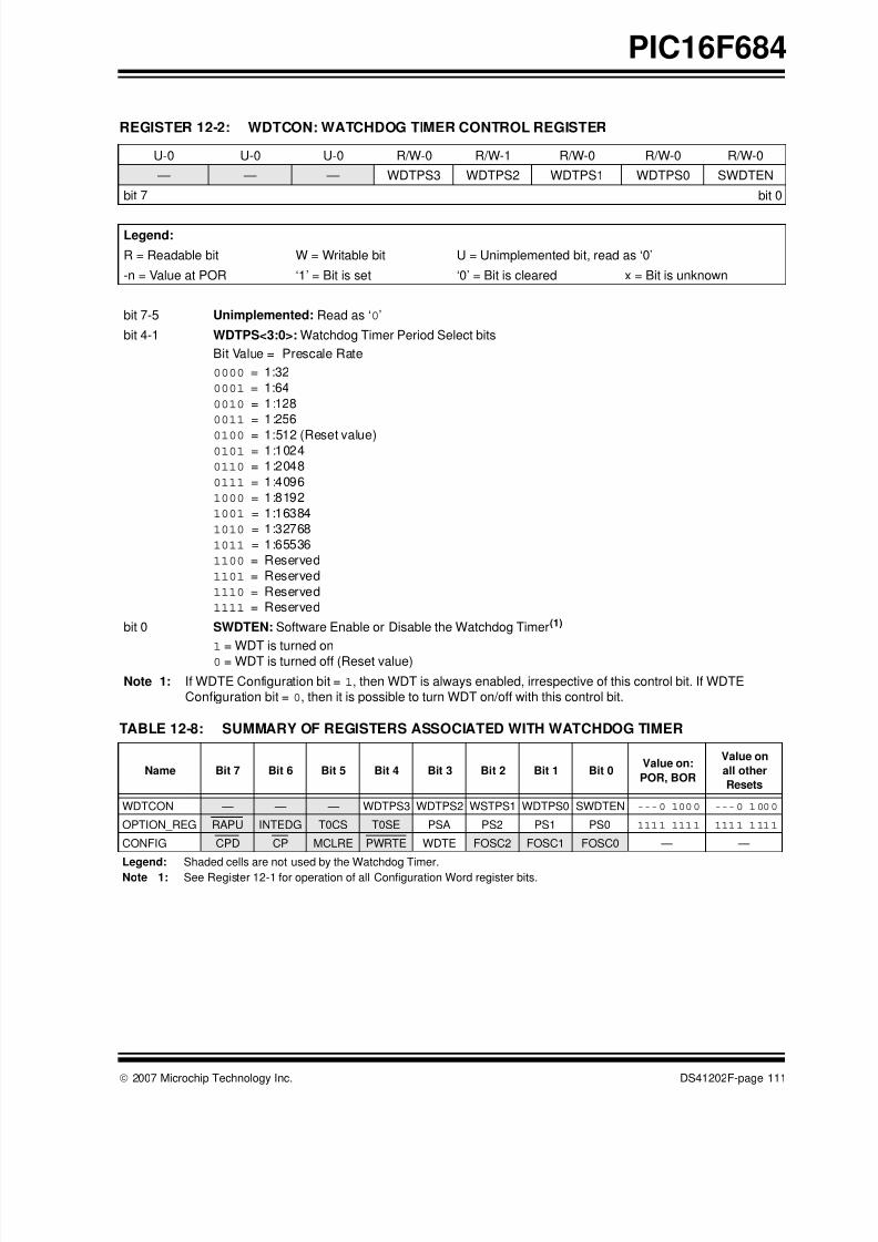
8/10/2019 PIC16F684 Datasheet
http://slidepdf.com/reader/full/pic16f684-datasheet 113/192
© 2007 Microchip Technology Inc. DS41202F-page 111
PIC16F684
TABLE 12-8: SUMMARY OF REGISTERS ASSOCIATED WITH WATCHDOG TIMER
REGISTER 12-2: WDTCON: WATCHDOG TIMER CONTROL REGISTER
U-0 U-0 U-0 R/W-0 R/W-1 R/W-0 R/W-0 R/W-0
— — — WDTPS3 WDTPS2 WDTPS1 WDTPS0 SWDTEN
bit 7 bit 0
Legend:
R = Readable bit W = Writable bit U = Unimplemented bit, read as ‘0’
-n = Value at POR ‘1’ = Bit is set ‘0’ = Bit is cleared x = Bit is unknown
bit 7-5 Unimplemented: Read as ‘0’
bit 4-1 WDTPS<3:0>: Watchdog Timer Period Select bits
Bit Value = Prescale Rate
0000 = 1:32
0001 = 1:64
0010 = 1:128
0011 = 1:256
0100 = 1:512 (Reset value)0101 = 1:1024
0110 = 1:2048
0111 = 1:4096
1000 = 1:8192
1001 = 1:16384
1010 = 1:32768
1011 = 1:65536
1100 = Reserved
1101 = Reserved
1110 = Reserved
1111 = Reserved
bit 0 SWDTEN: Software Enable or Disable the Watchdog Timer(1)
1 = WDT is turned on
0 = WDT is turned off (Reset value)
Note 1: If WDTE Configuration bit = 1, then WDT is always enabled, irrespective of this control bit. If WDTE
Configuration bit = 0, then it is possible to turn WDT on/off with this control bit.
Name Bit 7 Bit 6 Bit 5 Bit 4 Bit 3 Bit 2 Bit 1 Bit 0Value on:
POR, BOR
Value on
all other
Resets
WDTCON — — — WDTPS3 WDTPS2 WSTPS1 WDTPS0 SWDTEN ---0 1000 ---0 1000
OPTION_REG RAPU INTEDG T0CS T0SE PSA PS2 PS1 PS0 1111 1111 1111 1111
CONFIG CPD CP MCLRE PWRTE WDTE FOSC2 FOSC1 FOSC0 — —
Legend: Shaded cells are not used by the Watchdog Timer.
Note 1: See Register 12-1 for operation of all Configuration Word register bits.
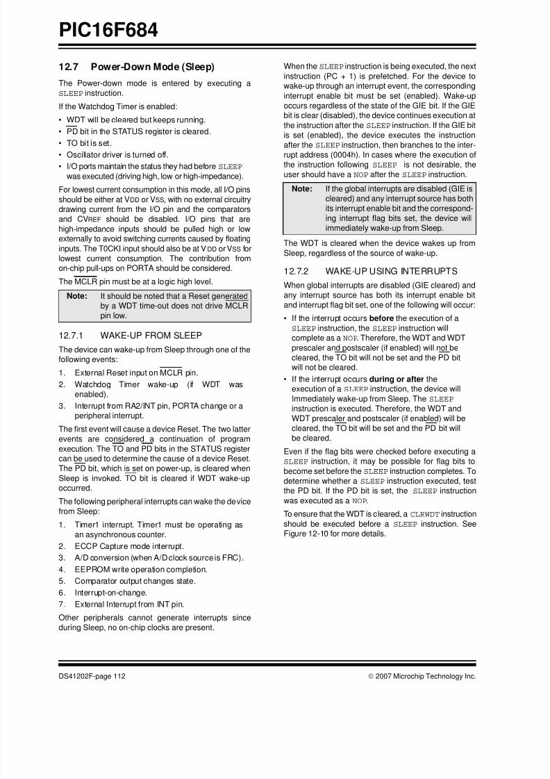
8/10/2019 PIC16F684 Datasheet
http://slidepdf.com/reader/full/pic16f684-datasheet 114/192
PIC16F684
DS41202F-page 112 © 2007 Microchip Technology Inc.
12.7 Power-Down Mode (Sleep)
The Power-down mode is entered by executing a
SLEEP instruction.
If the Watchdog Timer is enabled:
• WDT will be cleared but keeps running.
• PD bit in the STATUS register is cleared.
• TO bit is set.
• Oscillator driver is turned off.
• I/O ports maintain the status they had beforeSLEEP
was executed (driving high, low or high-impedance).
For lowest current consumption in this mode, all I/O pins
should be either at VDD or VSS, with no external circuitry
drawing current from the I/O pin and the comparators
and CVREF should be disabled. I/O pins that are
high-impedance inputs should be pulled high or low
externally to avoid switching currents caused by floating
inputs. The T0CKI input should also be at VDD or VSS for
lowest current consumption. The contribution from
on-chip pull-ups on PORTA should be considered.
The MCLR pin must be at a logic high level.
12.7.1 WAKE-UP FROM SLEEP
The device can wake-up from Sleep through one of the
following events:
1. External Reset input on MCLR pin.
2. Watchdog Timer wake-up (if WDT was
enabled).
3. Interrupt from RA2/INT pin, PORTA change or aperipheral interrupt.
The first event will cause a device Reset. The two latter
events are considered a continuation of program
execution. The TO and PD bits in the STATUS register
can be used to determine the cause of a device Reset.
The PD bit, which is set on power-up, is cleared when
Sleep is invoked. TO bit is cleared if WDT wake-up
occurred.
The following peripheral interrupts can wake the device
from Sleep:
1. Timer1 interrupt. Timer1 must be operating as
an asynchronous counter.
2. ECCP Capture mode interrupt.3. A/D conversion (when A/D clock source is FRC).
4. EEPROM write operation completion.
5. Comparator output changes state.
6. Interrupt-on-change.
7. External Interrupt from INT pin.
Other peripherals cannot generate interrupts since
during Sleep, no on-chip clocks are present.
When the SLEEP instruction is being executed, the next
instruction (PC + 1) is prefetched. For the device to
wake-up through an interrupt event, the corresponding
interrupt enable bit must be set (enabled). Wake-up
occurs regardless of the state of the GIE bit. If the GIE
bit is clear (disabled), the device continues execution at
the instruction after the SLEEP instruction. If the GIE bit
is set (enabled), the device executes the instructionafter the SLEEP instruction, then branches to the inter-
rupt address (0004h). In cases where the execution of
the instruction following SLEEP is not desirable, the
user should have a NOP after the SLEEP instruction.
The WDT is cleared when the device wakes up from
Sleep, regardless of the source of wake-up.
12.7.2 WAKE-UP USING INTERRUPTSWhen global interrupts are disabled (GIE cleared) and
any interrupt source has both its interrupt enable bit
and interrupt flag bit set, one of the following will occur:
• If the interrupt occurs before the execution of a
SLEEP instruction, the SLEEP instruction will
complete as a NOP. Therefore, the WDT and WDT
prescaler and postscaler (if enabled) will not be
cleared, the TO bit will not be set and the PD bit
will not be cleared.
• If the interrupt occurs during or after the
execution of a SLEEP instruction, the device will
Immediately wake-up from Sleep. The SLEEP
instruction is executed. Therefore, the WDT andWDT prescaler and postscaler (if enabled) will be
cleared, the TO bit will be set and the PD bit will
be cleared.
Even if the flag bits were checked before executing a
SLEEP instruction, it may be possible for flag bits to
become set before the SLEEP instruction completes. To
determine whether a SLEEP instruction executed, test
the PD bit. If the PD bit is set, the SLEEP instruction
was executed as a NOP.
To ensure that the WDT is cleared, a CLRWDT instruction
should be executed before a SLEEP instruction. See
Figure 12-10 for more details.
Note: It should be noted that a Reset generated
by a WDT time-out does not drive MCLR
pin low.
Note: If the global interrupts are disabled (GIE is
cleared) and any interrupt source has both
its interrupt enable bit and the correspond-
ing interrupt flag bits set, the device will
immediately wake-up from Sleep.
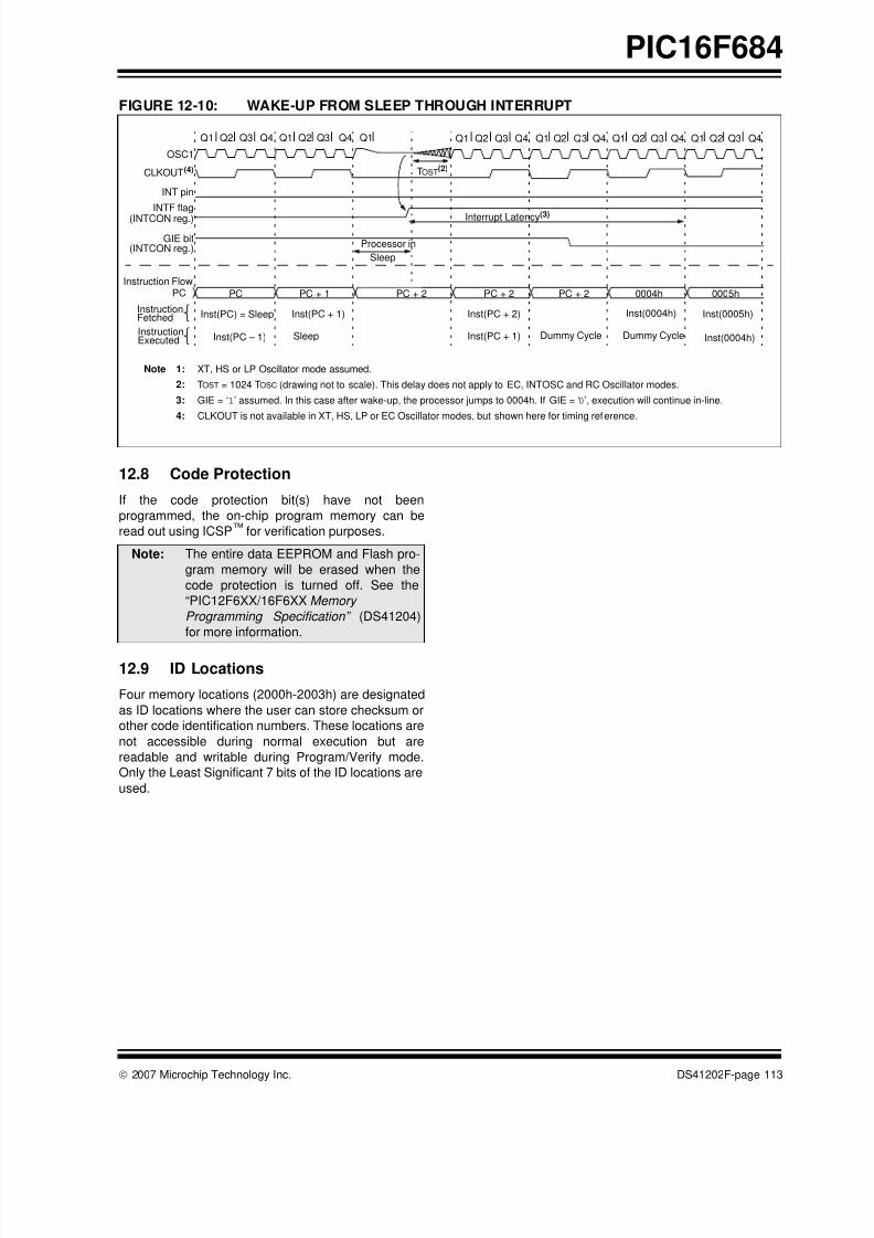
8/10/2019 PIC16F684 Datasheet
http://slidepdf.com/reader/full/pic16f684-datasheet 115/192
© 2007 Microchip Technology Inc. DS41202F-page 113
PIC16F684
FIGURE 12-10: WAKE-UP FROM SLEEP THROUGH INTERRUPT
12.8 Code Protection
If the code protection bit(s) have not been
programmed, the on-chip program memory can be
read out using ICSP™ for verification purposes.
12.9 ID Locations
Four memory locations (2000h-2003h) are designated
as ID locations where the user can store checksum or
other code identification numbers. These locations are
not accessible during normal execution but are
readable and writable during Program/Verify mode.
Only the Least Significant 7 bits of the ID locations are
used.
Q1 Q2 Q3 Q4 Q1 Q2 Q3 Q4 Q1 Q1 Q2 Q3 Q4 Q1 Q2 Q3 Q4 Q1 Q2 Q3 Q4 Q1 Q2 Q3 Q4
OSC1
CLKOUT(4)
INT pin
INTF flag
(INTCON reg.)
GIE bit(INTCON reg.)
Instruction FlowPC
InstructionFetched
InstructionExecuted
PC PC + 1 PC + 2
Inst(PC) = Sleep
Inst(PC – 1)
Inst(PC + 1)
Sleep
Processor in
Sleep
Interrupt Latency(3)
Inst(PC + 2)
Inst(PC + 1)
Inst(0004h) Inst(0005h)
Inst(0004h)Dummy Cycle
PC + 2 0004h 0005h
Dummy Cycle
TOST(2)
PC + 2
Note 1: XT, HS or LP Oscillator mode assumed.
2: TOST = 1024 TOSC (drawing not to scale). This delay does not apply to EC, INTOSC and RC Oscillator modes.
3: GIE = ‘1’ assumed. In this case after wake-up, the processor jumps to 0004h. If GIE = ‘0’, execution will continue in-line.
4: CLKOUT is not available in XT, HS, LP or EC Oscillator modes, but shown here for timing reference.
Note: The entire data EEPROM and Flash pro-
gram memory will be erased when the
code protection is turned off. See the
“PIC12F6XX/16F6XX Memory
Programming Specification” (DS41204)
for more information.

8/10/2019 PIC16F684 Datasheet
http://slidepdf.com/reader/full/pic16f684-datasheet 116/192
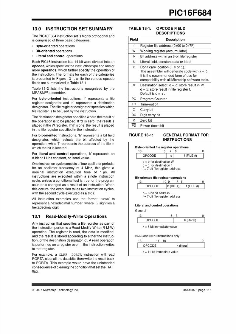
8/10/2019 PIC16F684 Datasheet
http://slidepdf.com/reader/full/pic16f684-datasheet 117/192
© 2007 Microchip Technology Inc. DS41202F-page 115
PIC16F684
13.0 INSTRUCTION SET SUMMARY
The PIC16F684 instruction set is highly orthogonal and
is comprised of three basic categories:
• Byte-oriented operations
• Bit-oriented operations
• Literal and control operations
Each PIC16 instruction is a 14-bit word divided into an
opcode, which specifies the instruction type and one or
more operands, which further specify the operation of
the instruction. The formats for each of the categories
is presented in Figure 13-1, while the various opcode
fields are summarized in Table 13-1.
Table 13-2 lists the instructions recognized by the
MPASMTM assembler.
For byte-oriented instructions, ‘f’ represents a file
register designator and ‘d’ represents a destination
designator. The file register designator specifies which
file register is to be used by the instruction.
The destination designator specifies where the result ofthe operation is to be placed. If ‘d’ is zero, the result is
placed in the W register. If ‘d’ is one, the result is placed
in the file register specified in the instruction.
For bit-oriented instructions, ‘b’ represents a bit field
designator, which selects the bit affected by the
operation, while ‘f’ represents the address of the file in
which the bit is located.
For literal and control operations, ‘k’ represents an
8-bit or 11-bit constant, or literal value.
One instruction cycle consists of four oscillator periods;
for an oscillator frequency of 4 MHz, this gives a
nominal instruction execution time of 1 µs. All
instructions are executed within a single instructioncycle, unless a conditional test is true, or the program
counter is changed as a result of an instruction. When
this occurs, the execution takes two instruction cycles,
with the second cycle executed as a NOP.
All instruction examples use the format ‘0xhh’ to
represent a hexadecimal number, where ‘h’ signifies a
hexadecimal digit.
13.1 Read-Modify-Write Operations
Any instruction that specifies a file register as part of
the instruction performs a Read-Modify-Write (R-M-W)
operation. The register is read, the data is modified,
and the result is stored according to either the instruc-
tion, or the destination designator ‘d’. A read operation
is performed on a register even if the instruction writes
to that register.
For example, a CLRF PORTA instruction will read
PORTA, clear all the data bits, then write the result back
to PORTA. This example would have the unintended
consequence of clearing the condition that set the RAIF
flag.
TABLE 13-1: OPCODE FIELD
DESCRIPTIONS
FIGURE 13-1: GENERAL FORMAT FOR
INSTRUCTIONS
Field Description
f Register file address (0x00 to 0x7F)
W Working register (accumulator)
b Bit address within an 8-bit file register
k Literal field, constant data or label
x Don’t care location (= 0 or 1).
The assembler will generate code with x = 0.
It is the recommended form of use for
compatibility with all Microchip software tools.
d Destination select; d = 0: store result in W,
d = 1: store result in file register f.
Default is d = 1.
PC Program Counter
TO Time-out bit
C Carry bit
DC Digit carry bit
Z Zero bit
PD Power-down bit
Byte-oriented file register operations
13 8 7 6 0
d = 0 for destination W
OPCODE d f (FILE #)
d = 1 for destination ff = 7-bit file register address
Bit-oriented file register operations
13 10 9 7 6 0
OPCODE b (BIT #) f (FILE #)
b = 3-bit bit addressf = 7-bit file register address
Literal and control operations
13 8 7 0
OPCODE k (literal)
k = 8-bit immediate value
13 11 10 0
OPCODE k (literal)
k = 11-bit immediate value
General
CALL and GOTO instructions only
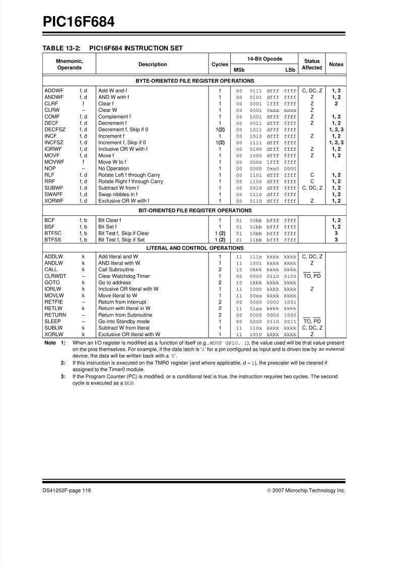
8/10/2019 PIC16F684 Datasheet
http://slidepdf.com/reader/full/pic16f684-datasheet 118/192
PIC16F684
DS41202F-page 116 © 2007 Microchip Technology Inc.
TABLE 13-2: PIC16F684 INSTRUCTION SET
Mnemonic,
OperandsDescription Cycles
14-Bit Opcode Status
AffectedNotes
MSb LSb
BYTE-ORIENTED FILE REGISTER OPERATIONS
ADDWF
ANDWFCLRF
CLRW
COMF
DECF
DECFSZ
INCF
INCFSZ
IORWF
MOVF
MOVWF
NOP
RLF
RRF
SUBWF
SWAPF
XORWF
f, d
f, df
–
f, d
f, d
f, d
f, d
f, d
f, d
f, d
f
–
f, d
f, d
f, d
f, d
f, d
Add W and f
AND W with fClear f
Clear W
Complement f
Decrement f
Decrement f, Skip if 0
Increment f
Increment f, Skip if 0
Inclusive OR W with f
Move f
Move W to f
No Operation
Rotate Left f through Carry
Rotate Right f through Carry
Subtract W from f
Swap nibbles in f
Exclusive OR W with f
1
11
1
1
1
1(2)
1
1(2)
1
1
1
1
1
1
1
1
1
00
0000
00
00
00
00
00
00
00
00
00
00
00
00
00
00
00
0111
01010001
0001
1001
0011
1011
1010
1111
0100
1000
0000
0000
1101
1100
0010
1110
0110
dfff
dffflfff
0xxx
dfff
dfff
dfff
dfff
dfff
dfff
dfff
lfff
0xx0
dfff
dfff
dfff
dfff
dfff
ffff
ffffffff
xxxx
ffff
ffff
ffff
ffff
ffff
ffff
ffff
ffff
0000
ffff
ffff
ffff
ffff
ffff
C, DC, Z
ZZ
Z
Z
Z
Z
Z
Z
C
C
C, DC, Z
Z
1, 2
1, 22
1, 2
1, 2
1, 2, 3
1, 2
1, 2, 3
1, 2
1, 2
1, 2
1, 2
1, 2
1, 2
1, 2
BIT-ORIENTED FILE REGISTER OPERATIONS
BCF
BSF
BTFSC
BTFSS
f, b
f, b
f, b
f, b
Bit Clear f
Bit Set f
Bit Test f, Skip if Clear
Bit Test f, Skip if Set
1
1
1 (2)
1 (2)
01
01
01
01
00bb
01bb
10bb
11bb
bfff
bfff
bfff
bfff
ffff
ffff
ffff
ffff
1, 2
1, 2
3
3
LITERAL AND CONTROL OPERATIONS
ADDLW
ANDLW
CALL
CLRWDT
GOTO
IORLW
MOVLWRETFIE
RETLW
RETURN
SLEEP
SUBLW
XORLW
k
k
k
–
k
k
k –
k
–
–
k
k
Add literal and W
AND literal with W
Call Subroutine
Clear Watchdog Timer
Go to address
Inclusive OR literal with W
Move literal to WReturn from interrupt
Return with literal in W
Return from Subroutine
Go into Standby mode
Subtract W from literal
Exclusive OR literal with W
1
1
2
1
2
1
12
2
2
1
1
1
11
11
10
00
10
11
1100
11
00
00
11
11
111x
1001
0kkk
0000
1kkk
1000
00xx0000
01xx
0000
0000
110x
1010
kkkk
kkkk
kkkk
0110
kkkk
kkkk
kkkk0000
kkkk
0000
0110
kkkk
kkkk
kkkk
kkkk
kkkk
0100
kkkk
kkkk
kkkk1001
kkkk
1000
0011
kkkk
kkkk
C, DC, Z
Z
TO, PD
Z
TO, PD
C, DC, Z
Z
Note 1: When an I/O register is modified as a function of itself (e.g., MOVF GPIO, 1), the value used will be that value present
on the pins themselves. For example, if the data latch is ‘1’ for a pin configured as input and is driven low by an external
device, the data will be written back with a ‘0’.
2: If this instruction is executed on the TMR0 register (and where applicable, d = 1), the prescaler will be cleared if
assigned to the Timer0 module.
3: If the Program Counter (PC) is modified, or a conditional test is true, the instruction requires two cycles. The second
cycle is executed as a NOP.
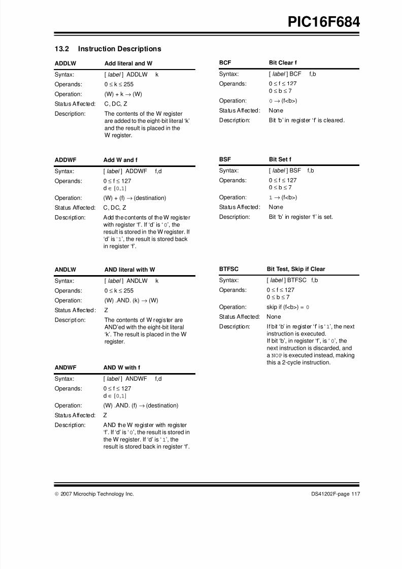
8/10/2019 PIC16F684 Datasheet
http://slidepdf.com/reader/full/pic16f684-datasheet 119/192
© 2007 Microchip Technology Inc. DS41202F-page 117
PIC16F684
13.2 Instruction Descriptions
ADDLW Add literal and W
Syntax: [ label ] ADDLW k
Operands: 0 ≤ k ≤ 255
Operation: (W) + k → (W)
Status Affected: C, DC, Z
Description: The contents of the W register
are added to the eight-bit literal ‘k’
and the result is placed in the
W register.
ADDWF Add W and f
Syntax: [ label ] ADDWF f,d
Operands: 0 ≤ f ≤ 127
d ∈ [0,1]
Operation: (W) + (f) → (destination)Status Affected: C, DC, Z
Description: Add the contents of the W register
with register ‘f’. If ‘d’ is ‘0’, the
result is stored in the W register. If
‘d’ is ‘1’, the result is stored back
in register ‘f’.
ANDLW AND literal with W
Syntax: [ label ] ANDLW k
Operands: 0 ≤ k ≤ 255
Operation: (W) .AND. (k) → (W)
Status Affected: Z
Description: The contents of W register are
AND’ed with the eight-bit literal
‘k’. The result is placed in the W
register.
ANDWF AND W with f
Syntax: [ label ] ANDWF f,d
Operands: 0 ≤ f ≤ 127
d ∈ [0,1]Operation: (W) .AND. (f) → (destination)
Status Affected: Z
Description: AND the W register with register
‘f’. If ‘d’ is ‘0’, the result is stored in
the W register. If ‘d’ is ‘1’, the
result is stored back in register ‘f’.
BCF Bit Clear f
Syntax: [ label ] BCF f,b
Operands: 0 ≤ f ≤ 127
0 ≤ b ≤ 7
Operation: 0 → (f<b>)
Status Affected: None
Description: Bit ‘b’ in register ‘f’ is cleared.
BSF Bit Set f
Syntax: [ label ] BSF f,b
Operands: 0 ≤ f ≤ 127
0 ≤ b ≤ 7
Operation: 1 → (f<b>)Status Affected: None
Description: Bit ‘b’ in register ‘f ’ is set.
BTFSC Bit Test, Skip if Clear
Syntax: [ label ] BTFSC f,b
Operands: 0 ≤ f ≤ 127
0 ≤ b ≤ 7Operation: skip if (f<b>) = 0
Status Affected: None
Description: If bit ‘b’ in register ‘f’ is ‘1’, the next
instruction is executed.
If bit ‘b’, in register ‘f’, is ‘0’, the
next instruction is discarded, and
a NOP is executed instead, making
this a 2-cycle instruction.

8/10/2019 PIC16F684 Datasheet
http://slidepdf.com/reader/full/pic16f684-datasheet 120/192
PIC16F684
DS41202F-page 118 © 2007 Microchip Technology Inc.
BTFSS Bit Test f, Skip if Set
Syntax: [ label ] BTFSS f,b
Operands: 0 ≤ f ≤ 127
0 ≤ b < 7
Operation: skip if (f<b>) = 1
Status Affected: None
Description: If bit ‘b’ in register ‘f’ is ‘0’, the next
instruction is executed.
If bit ‘b’ is ‘1’, then the next
instruction is discarded and a NOP
is executed instead, making this a
2-cycle instruction.
CALL Call Subroutine
Syntax: [ label ] CALL k
Operands: 0 ≤ k ≤ 2047
Operation: (PC)+ 1→ TOS,
k → PC<10:0>,
(PCLATH<4:3>) → PC<12:11>
Status Affected: None
Description: Call Subroutine. First, return
address (PC + 1) is pushed onto
the stack. The eleven-bit
immediate address is loaded into
PC bits <10:0>. The upper bits of
the PC are loaded from PCLATH.
CALL is a two-cycle instruction.
CLRF Clear f
Syntax: [ label ] CLRF f
Operands: 0 ≤ f ≤ 127
Operation: 00h → (f)
1 → Z
Status Affected: Z
Description: The contents of register ‘f ’ are
cleared and the Z bit is set.
CLRW Clear W
Syntax: [ label ] CLRW
Operands: None
Operation: 00h → (W)
1 → Z
Status Affected: Z
Description: W register is cleared. Zero bit (Z)
is set.
CLRWDT Clear Watchdog Timer
Syntax: [ label ] CLRWDT
Operands: None
Operation: 00h → WDT
0 → WDT prescaler,1 → TO
1 → PD
Status Affected: TO, PD
Description: CLRWDT instruction resets the
Watchdog Timer. It also resets the
prescaler of the WDT.
Status bits TO and PD are set.
COMF Complement f
Syntax: [ label ] COMF f,d
Operands: 0 ≤ f ≤ 127
d ∈ [0,1]
Operation: (f) → (destination)
Status Affected: Z
Description: The contents of register ‘f’ are
complemented. If ‘d’ is ‘0’, the
result is stored in W. If ‘d’ is ‘1’,
the result is stored back in
register ‘f’.
DECF Decrement f
Syntax: [ label ] DECF f,d
Operands: 0 ≤ f ≤ 127
d ∈ [0,1]
Operation: (f) - 1 → (destination)
Status Affected: Z
Description: Decrement register ‘f ’. If ‘d’ is ‘0’,
the result is stored in the W
register. If ‘d’ is ‘1’, the result is
stored back in register ‘f’.
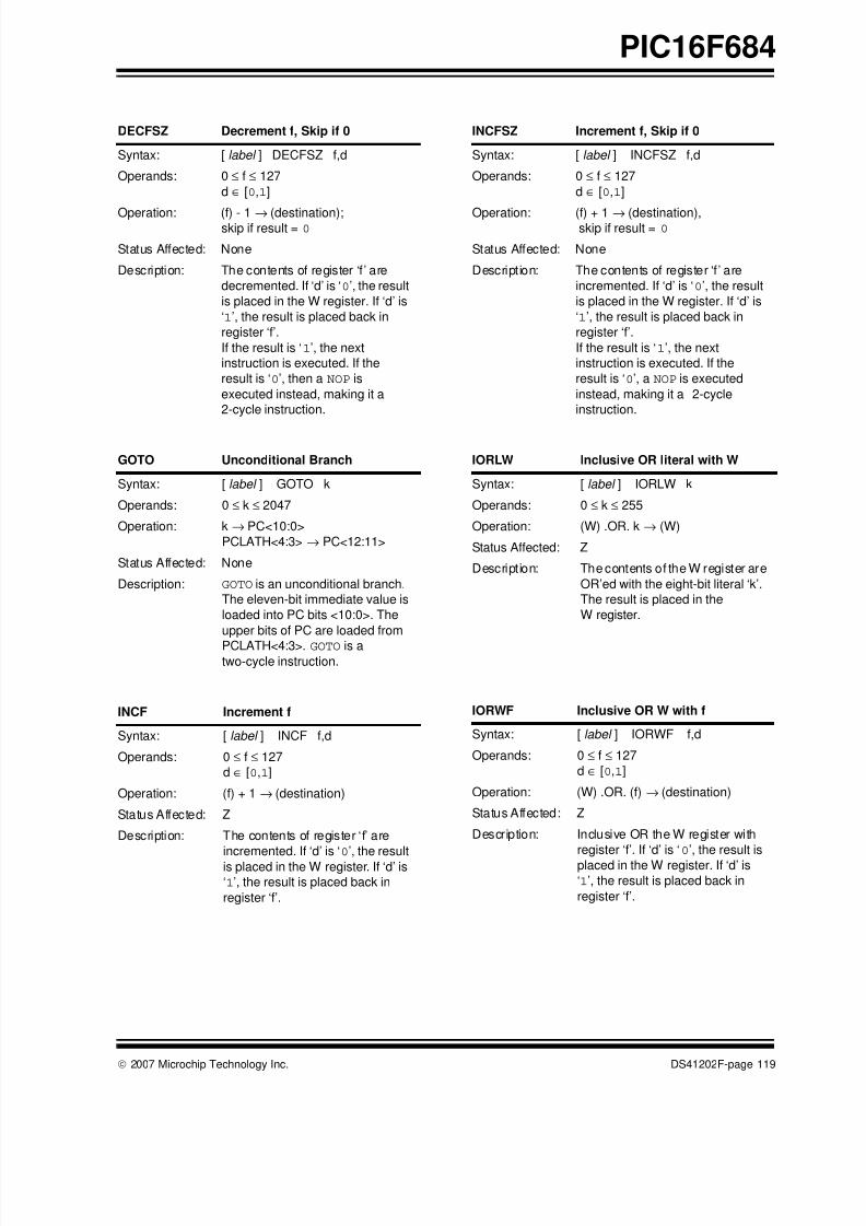
8/10/2019 PIC16F684 Datasheet
http://slidepdf.com/reader/full/pic16f684-datasheet 121/192
© 2007 Microchip Technology Inc. DS41202F-page 119
PIC16F684
DECFSZ Decrement f, Skip if 0
Syntax: [ label ] DECFSZ f,d
Operands: 0 ≤ f ≤ 127
d ∈ [0,1]
Operation: (f) - 1 → (destination);skip if result = 0
Status Affected: None
Description: The contents of register ‘f ’ are
decremented. If ‘d’ is ‘0’, the result
is placed in the W register. If ‘d’ is
‘1’, the result is placed back in
register ‘f’.
If the result is ‘1’, the next
instruction is executed. If the
result is ‘0’, then a NOP is
executed instead, making it a
2-cycle instruction.
GOTO Unconditional Branch
Syntax: [ label ] GOTO k
Operands: 0 ≤ k ≤ 2047
Operation: k → PC<10:0>
PCLATH<4:3> → PC<12:11>
Status Affected: None
Description: GOTO is an unconditional branch.
The eleven-bit immediate value is
loaded into PC bits <10:0>. The
upper bits of PC are loaded from
PCLATH<4:3>. GOTO is atwo-cycle instruction.
INCF Increment f
Syntax: [ label ] INCF f,d
Operands: 0 ≤ f ≤ 127
d ∈ [0,1]
Operation: (f) + 1 → (destination)
Status Affected: Z
Description: The contents of register ‘f’ are
incremented. If ‘d’ is ‘0’, the result
is placed in the W register. If ‘d’ is
‘1’, the result is placed back in
register ‘f’.
INCFSZ Increment f, Skip if 0
Syntax: [ label ] INCFSZ f,d
Operands: 0 ≤ f ≤ 127
d ∈ [0,1]
Operation: (f) + 1 → (destination), skip if result = 0
Status Affected: None
Description: The contents of register ‘f ’ are
incremented. If ‘d’ is ‘0’, the result
is placed in the W register. If ‘d’ is
‘1’, the result is placed back in
register ‘f’.
If the result is ‘1’, the next
instruction is executed. If the
result is ‘0’, a NOP is executed
instead, making it a 2-cycle
instruction.
IORLW Inclusive OR literal with W
Syntax: [ label ] IORLW k
Operands: 0 ≤ k ≤ 255
Operation: (W) .OR. k → (W)
Status Affected: Z
Description: The contents of the W register are
OR’ed with the eight-bit literal ‘k’.
The result is placed in the
W register.
IORWF Inclusive OR W with f
Syntax: [ label ] IORWF f,d
Operands: 0 ≤ f ≤ 127
d ∈ [0,1]
Operation: (W) .OR. (f) → (destination)
Status Affected: Z
Description: Inclusive OR the W register with
register ‘f’. If ‘d’ is ‘0’, the result is
placed in the W register. If ‘d’ is
‘1’, the result is placed back in
register ‘f’.
8/10/2019 PIC16F684 Datasheet
http://slidepdf.com/reader/full/pic16f684-datasheet 122/192
PIC16F684
DS41202F-page 120 © 2007 Microchip Technology Inc.
MOVF Move f
Syntax: [ label ] MOVF f,d
Operands: 0 ≤ f ≤ 127
d ∈ [0,1]
Operation: (f) → (dest)Status Affected: Z
Description: The contents of register f is
moved to a destination dependent
upon the status of d. If d = 0,
destination is W register. If d = 1,
the destination is file register f
itself. d = 1 is useful to test a file
register since status flag Z is
affected.
Words: 1
Cycles: 1
Example: MOVF FSR, 0
After Instruction
W = value in FSR
register
Z = 1
MOVLW Move literal to W
Syntax: [ label ] MOVLW k
Operands: 0 ≤ k ≤ 255
Operation: k → (W)
Status Affected: None
Description: The eight-bit literal ‘k’ is loaded into
W register. The “don’t cares” will
assemble as ‘0’s.
Words: 1
Cycles: 1
Example: MOVLW 0x5A
After Instruction
W = 0x5A
MOVWF Move W to f
Syntax: [ label ] MOVWF f
Operands: 0 ≤ f ≤ 127
Operation: (W) → (f)
Status Affected: None
Description: Move data from W register to
register ‘f’.
Words: 1
Cycles: 1
Example: MOVW
F
OPTION
Before Instruction
OPTION = 0xFF
W = 0x4F
After Instruction
OPTION = 0x4F
W = 0x4F
NOP No Operation
Syntax: [ label ] NOP
Operands: None
Operation: No operation
Status Affected: None
Description: No operation.
Words: 1
Cycles: 1
Example: NOP
8/10/2019 PIC16F684 Datasheet
http://slidepdf.com/reader/full/pic16f684-datasheet 123/192
© 2007 Microchip Technology Inc. DS41202F-page 121
PIC16F684
RETFIE Return from Interrupt
Syntax: [ label ] RETFIE
Operands: None
Operation: TOS → PC,
1 → GIEStatus Affected: None
Description: Return from Interrupt. Stack is
POPed and Top-of-Stack (TOS) is
loaded in the PC. Interrupts are
enabled by setting Global
Interrupt Enable bit, GIE
(INTCON<7>). This is a two-cycle
instruction.
Words: 1
Cycles: 2
Example: RETFIE
After InterruptPC = TOS
GIE = 1
RETLW Return with literal in W
Syntax: [ label ] RETLW k
Operands: 0 ≤ k ≤ 255
Operation: k → (W);
TOS → PCStatus Affected: None
Description: The W register is loaded with the
eight bit literal ‘k’. The program
counter is loaded from the top of
the stack (the return address).
This is a two-cycle instruction.
Words: 1
Cycles: 2
Example:
TABLE
CALL TABLE;W containstable
;offset value
• ;W now has table value
•
•
ADDWF PC ;W = offset
RETLW k1 ;Begin table
RETLW k2 ;
•
•
•
RETLW kn ; End of table
Before Instruction
W = 0x07
After Instruction
W = value of k8
RETURN Return from Subroutine
Syntax: [ label ] RETURN
Operands: None
Operation: TOS → PC
Status Affected: None
Description: Return from subroutine. The stack
is POPed and the top of the stack
(TOS) is loaded into the program
counter. This is a two-cycle
instruction.

8/10/2019 PIC16F684 Datasheet
http://slidepdf.com/reader/full/pic16f684-datasheet 124/192
PIC16F684
DS41202F-page 122 © 2007 Microchip Technology Inc.
RLF Rotate Left f through Carry
Syntax: [ label ] RLF f,d
Operands: 0 ≤ f ≤ 127
d ∈ [0,1]
Operation: See description below
Status Affected: C
Description: The contents of register ‘f’ are
rotated one bit to the left through
the Carry flag. If ‘d’ is ‘0’, the
result is placed in the W register.
If ‘d’ is ‘1’, the result is stored
back in register ‘f’.
Words: 1
Cycles: 1
Example: RLF REG1,0
Before InstructionREG1 = 1110 0110
C = 0
After InstructionREG1 = 1110 0110
W = 1100 1100
C = 1
RRF Rotate Right f through Carry
Syntax: [ label ] RRF f,d
Operands: 0 ≤ f ≤ 127
d ∈ [0,1]Operation: See description below
Status Affected: C
Description: The contents of register ‘f ’ are
rotated one bit to the right through
the Carry flag. If ‘d’ is ‘0’, the
result is placed in the W register.
If ‘d’ is ‘1’, the result is placed
back in register ‘f’.
Register fC
Register fC
SLEEP Enter Sleep mode
Syntax: [ label ] SLEEP
Operands: None
Operation: 00h → WDT,
0 → WDT prescaler,
1 → TO,
0 → PD
Status Affected: TO, PD
Description: The power-down Status bit, PD is
cleared. Time-out Status bit, TO
is set. Watchdog Timer and its
prescaler are cleared.
The processor is put into Sleep
mode with the oscillator stopped.
SUBLW Subtract W from literal
Syntax: [ label ] SUBLW k
Operands: 0 ≤ k ≤ 255
Operation: k - (W) → (W)
Status Affected: C, DC, Z
Description: The W register is subtracted (2’s
complement method) from the
eight-bit literal ‘k’. The result is
placed in the W register.
C = 0 W > k
C = 1 W ≤ k
DC = 0 W<3:0> > k<3:0>
DC = 1 W<3:0> ≤ k<3:0>
8/10/2019 PIC16F684 Datasheet
http://slidepdf.com/reader/full/pic16f684-datasheet 125/192
© 2007 Microchip Technology Inc. DS41202F-page 123
PIC16F684
SUBWF Subtract W from f
Syntax: [ label ] SUBWF f,d
Operands: 0 ≤ f ≤ 127
d ∈ [0,1]
Operation: (f) - (W) → (destination)Status Affected: C, DC, Z
Description: Subtract (2’s complement method)
W register from register ‘f’. If ‘d’ is
‘0’, the result is stored in the W
register. If ‘d’ is ‘1’, the result is
stored back in register ‘f.
SWAPF Swap Nibbles in f
Syntax: [ label ] SWAPF f,d
Operands: 0 ≤ f ≤ 127
d ∈ [0,1]
Operation: (f<3:0>) → (destination<7:4>),
(f<7:4>) → (destination<3:0>)
Status Affected: None
Description: The upper and lower nibbles of
register ‘f’ are exchanged. If ‘d’ is‘0’, the result is placed in the W
register. If ‘d’ is ‘1’, the result is
placed in register ‘f’.
C = 0 W > f
C = 1 W ≤ f
DC = 0 W<3:0> > f<3:0>
DC = 1 W<3:0> ≤ f<3:0>
XORLW Exclusive OR literal with W
Syntax: [ label ] XORLW k
Operands: 0 ≤ k ≤ 255
Operation: (W) .XOR. k → (W)
Status Affected: Z
Description: The contents of the W register
are XOR’ed with the eight-bit
literal ‘k’. The result is placed in
the W register.
XORWF Exclusive OR W with f
Syntax: [ label ] XORWF f,d
Operands: 0 ≤ f ≤ 127
d ∈ [0,1]
Operation: (W) .XOR. (f) → (destination)
Status Affected: Z
Description: Exclusive OR the contents of the
W register with register ‘f’. If ‘d’ is
‘0’, the result is stored in the Wregister. If ‘d’ is ‘1’, the result is
stored back in register ‘f’.

8/10/2019 PIC16F684 Datasheet
http://slidepdf.com/reader/full/pic16f684-datasheet 126/192
PIC16F684
DS41202F-page 124 © 2007 Microchip Technology Inc.
NOTES:
8/10/2019 PIC16F684 Datasheet
http://slidepdf.com/reader/full/pic16f684-datasheet 127/192
© 2007 Microchip Technology Inc. DS41202F-page 125
PIC16F684
14.0 DEVELOPMENT SUPPORT
The PIC ® microcontrollers are supported with a full
range of hardware and software development tools:
• Integrated Development Environment
- MPLAB ® IDE Software
• Assemblers/Compilers/Linkers
- MPASMTM Assembler
- MPLAB C18 and MPLAB C30 C Compilers
- MPLINKTM Object Linker/
MPLIBTM Object Librarian
- MPLAB ASM30 Assembler/Linker/Library
• Simulators
- MPLAB SIM Software Simulator
• Emulators
- MPLAB ICE 2000 In-Circuit Emulator
- MPLAB REAL ICE™ In-Circuit Emulator
• In-Circuit Debugger
- MPLAB ICD 2
• Device Programmers
- PICSTART ® Plus Development Programmer
- MPLAB PM3 Device Programmer
- PICkit™ 2 Development Programmer
• Low-Cost Demonstration and Development
Boards and Evaluation Kits
14.1 MPLAB Integrated DevelopmentEnvironment Software
The MPLAB IDE software brings an ease of software
development previously unseen in the 8/16-bit micro-
controller market. The MPLAB IDE is a Windows ®
operating system-based application that contains:
• A single graphical interface to all debugging tools
- Simulator
- Programmer (sold separately)
- Emulator (sold separately)
- In-Circuit Debugger (sold separately)
• A full-featured editor with color-coded context
• A multiple project manager
• Customizable data windows with direct edit of
contents
• High-level source code debugging
• Visual device initializer for easy register
initialization
• Mouse over variable inspection• Drag and drop variables from source to watch
windows
• Extensive on-line help
• Integration of select third party tools, such as
HI-TECH Software C Compilers and IAR
C Compilers
The MPLAB IDE allows you to:
• Edit your source files (either assembly or C)
• One touch assemble (or compile) and download
to PIC MCU emulator and simulator tools
(automatically updates all project information)
• Debug using:- Source files (assembly or C)
- Mixed assembly and C
- Machine code
MPLAB IDE supports multiple debugging tools in a
single development paradigm, from the cost-effective
simulators, through low-cost in-circuit debuggers, to
full-featured emulators. This eliminates the learning
curve when upgrading to tools with increased flexibility
and power.
8/10/2019 PIC16F684 Datasheet
http://slidepdf.com/reader/full/pic16f684-datasheet 128/192
PIC16F684
DS41202F-page 126 © 2007 Microchip Technology Inc.
14.2 MPASM Assembler
The MPASM Assembler is a full-featured, universal
macro assembler for all PIC MCUs.
The MPASM Assembler generates relocatable object
files for the MPLINK Object Linker, Intel ® standard HEX
files, MAP files to detail memory usage and symbol
reference, absolute LST files that contain source linesand generated machine code and COFF files for
debugging.
The MPASM Assembler features include:
• Integration into MPLAB IDE projects
• User-defined macros to streamline
assembly code
• Conditional assembly for multi-purpose
source files
• Directives that allow complete control over the
assembly process
14.3 MPLAB C18 and MPLAB C30C Compilers
The MPLAB C18 and MPLAB C30 Code Development
Systems are complete ANSI C compilers for
Microchip’s PIC18 and PIC24 families of microcontrol-
lers and the dsPIC30 and dsPIC33 family of digital sig-
nal controllers. These compilers provide powerful
integration capabilities, superior code optimization and
ease of use not found with other compilers.
For easy source level debugging, the compilers provide
symbol information that is optimized to the MPLAB IDE
debugger.
14.4 MPLINK Object Linker/MPLIB Object Librarian
The MPLINK Object Linker combines relocatable
objects created by the MPASM Assembler and the
MPLAB C18 C Compiler. It can link relocatable objects
from precompiled libraries, using directives from a
linker script.
The MPLIB Object Librarian manages the creation and
modification of library files of precompiled code. When
a routine from a library is called from a source file, only
the modules that contain that routine will be linked in
with the application. This allows large libraries to be
used efficiently in many different applications.
The object linker/library features include:
• Efficient linking of single libraries instead of many
smaller files
• Enhanced code maintainability by grouping
related modules together
• Flexible creation of libraries with easy module
listing, replacement, deletion and extraction
14.5 MPLAB ASM30 Assembler, Linkerand Librarian
MPLAB ASM30 Assembler produces relocatable
machine code from symbolic assembly language for
dsPIC30F devices. MPLAB C30 C Compiler uses the
assembler to produce its object file. The assembler
generates relocatable object files that can then bearchived or linked with other relocatable object files and
archives to create an executable file. Notable features
of the assembler include:
• Support for the entire dsPIC30F instruction set
• Support for fixed-point and floating-point data
• Command line interface
• Rich directive set
• Flexible macro language
• MPLAB IDE compatibility
14.6 MPLAB SIM Software Simulator
The MPLAB SIM Software Simulator allows codedevelopment in a PC-hosted environment by simulat-
ing the PIC MCUs and dsPIC ® DSCs on an instruction
level. On any given instruction, the data areas can be
examined or modified and stimuli can be applied from
a comprehensive stimulus controller. Registers can be
logged to files for further run-time analysis. The trace
buffer and logic analyzer display extend the power of
the simulator to record and track program execution,
actions on I/O, most peripherals and internal registers.
The MPLAB SIM Software Simulator fully supports
symbolic debugging using the MPLAB C18 and
MPLAB C30 C Compilers, and the MPASM and
MPLAB ASM30 Assemblers. The software simulator
offers the flexibility to develop and debug code outside
of the hardware laboratory environment, making it an
excellent, economical software development tool.

8/10/2019 PIC16F684 Datasheet
http://slidepdf.com/reader/full/pic16f684-datasheet 129/192
© 2007 Microchip Technology Inc. DS41202F-page 127
PIC16F684
14.7 MPLAB ICE 2000High-PerformanceIn-Circuit Emulator
The MPLAB ICE 2000 In-Circuit Emulator is intended
to provide the product development engineer with a
complete microcontroller design tool set for PIC
microcontrollers. Software control of the MPLAB ICE2000 In-Circuit Emulator is advanced by the MPLAB
Integrated Development Environment, which allows
editing, building, downloading and source debugging
from a single environment.
The MPLAB ICE 2000 is a full-featured emulator
system with enhanced trace, trigger and data monitor-
ing features. Interchangeable processor modules allow
the system to be easily reconfigured for emulation of
different processors. The architecture of the MPLAB
ICE 2000 In-Circuit Emulator allows expansion to
support new PIC microcontrollers.
The MPLAB ICE 2000 In-Circuit Emulator system has
been designed as a real-time emulation system withadvanced features that are typically found on more
expensive development tools. The PC platform and
Microsoft ® Windows ® 32-bit operating system were
chosen to best make these features available in a
simple, unified application.
14.8 MPLAB REAL ICE In-CircuitEmulator System
MPLAB REAL ICE In-Circuit Emulator System is
Microchip’s next generation high-speed emulator for
Microchip Flash DSC ® and MCU devices. It debugs and
programs PIC ® and dsPIC ® Flash microcontrollers with
the easy-to-use, powerful graphical user interface of theMPLAB Integrated Development Environment (IDE),
included with each kit.
The MPLAB REAL ICE probe is connected to the design
engineer’s PC using a high-speed USB 2.0 interface and
is connected to the target with either a connector
compatible with the popular MPLAB ICD 2 system
(RJ11) or with the new high speed, noise tolerant, low-
voltage differential signal (LVDS) interconnection
(CAT5).
MPLAB REAL ICE is field upgradeable through future
firmware downloads in MPLAB IDE. In upcoming
releases of MPLAB IDE, new devices will be supported,
and new features will be added, such as software break-points and assembly code trace. MPLAB REAL ICE
offers significant advantages over competitive emulators
including low-cost, full-speed emulation, real-time
variable watches, trace analysis, complex breakpoints, a
ruggedized probe interface and long (up to three meters)
interconnection cables.
14.9 MPLAB ICD 2 In-Circuit Debugger
Microchip’s In-Circuit Debugger, MPLAB ICD 2, is a
powerful, low-cost, run-time development tool,
connecting to the host PC via an RS-232 or high-speed
USB interface. This tool is based on the Flash PIC
MCUs and can be used to develop for these and other
PIC MCUs and dsPIC DSCs. The MPLAB ICD 2 utilizesthe in-circuit debugging capability built into the Flash
devices. This feature, along with Microchip’s In-Circuit
Serial ProgrammingTM (ICSPTM) protocol, offers cost-
effective, in-circuit Flash debugging from the graphical
user interface of the MPLAB Integrated Development
Environment. This enables a designer to develop and
debug source code by setting breakpoints, single step-
ping and watching variables, and CPU status and
peripheral registers. Running at full speed enables
testing hardware and applications in real time. MPLAB
ICD 2 also serves as a development programmer for
selected PIC devices.
14.10 MPLAB PM3 Device ProgrammerThe MPLAB PM3 Device Programmer is a universal,
CE compliant device programmer with programmable
voltage verification at VDDMIN and VDDMAX for
maximum reliability. It features a large LCD display
(128 x 64) for menus and error messages and a modu-
lar, detachable socket assembly to support various
package types. The ICSP™ cable assembly is included
as a standard item. In Stand-Alone mode, the MPLAB
PM3 Device Programmer can read, verify and program
PIC devices without a PC connection. It can also set
code protection in this mode. The MPLAB PM3
connects to the host PC via an RS-232 or USB cable.
The MPLAB PM3 has high-speed communications andoptimized algorithms for quick programming of large
memory devices and incorporates an SD/MMC card for
file storage and secure data applications.
8/10/2019 PIC16F684 Datasheet
http://slidepdf.com/reader/full/pic16f684-datasheet 130/192
PIC16F684
DS41202F-page 128 © 2007 Microchip Technology Inc.
14.11 PICSTART Plus DevelopmentProgrammer
The PICSTART Plus Development Programmer is an
easy-to-use, low-cost, prototype programmer. It
connects to the PC via a COM (RS-232) port. MPLAB
Integrated Development Environment software makes
using the programmer simple and efficient. ThePICSTART Plus Development Programmer supports
most PIC devices in DIP packages up to 40 pins.
Larger pin count devices, such as the PIC16C92X and
PIC17C76X, may be supported with an adapter socket.
The PICSTART Plus Development Programmer is CE
compliant.
14.12 PICkit 2 Development Programmer
The PICkit™ 2 Development Programmer is a low-cost
programmer and selected Flash device debugger with
an easy-to-use interface for programming many of
Microchip’s baseline, mid-range and PIC18F families of
Flash memory microcontrollers. The PICkit 2 Starter Kitincludes a prototyping development board, twelve
sequential lessons, software and HI-TECH’s PICC™
Lite C compiler, and is designed to help get up to speed
quickly using PIC ® microcontrollers. The kit provides
everything needed to program, evaluate and develop
applications using Microchip’s powerful, mid-range
Flash memory family of microcontrollers.
14.13 Demonstration, Development andEvaluation Boards
A wide variety of demonstration, development and
evaluation boards for various PIC MCUs and dsPIC
DSCs allows quick application development on fully func-
tional systems. Most boards include prototyping areas for
adding custom circuitry and provide application firmwareand source code for examination and modification.
The boards support a variety of features, including LEDs,
temperature sensors, switches, speakers, RS-232
interfaces, LCD displays, potentiometers and additional
EEPROM memory.
The demonstration and development boards can be
used in teaching environments, for prototyping custom
circuits and for learning about various microcontroller
applications.
In addition to the PICDEM™ and dsPICDEM™ demon-
stration/development board series of circuits, Microchip
has a line of evaluation kits and demonstration software
for analog filter design, KEELOQ ® security ICs, CAN,IrDA ® , PowerSmart ® battery management, SEEVAL ®
evaluation system, Sigma-Delta ADC, flow rate
sensing, plus many more.
Check the Microchip web page (www.microchip.com)
and the latest “Product Selector Guide” (DS00148) for
the complete list of demonstration, development and
evaluation kits.
8/10/2019 PIC16F684 Datasheet
http://slidepdf.com/reader/full/pic16f684-datasheet 131/192
© 2007 Microchip Technology Inc. DS41202F-page 129
PIC16F684
15.0 ELECTRICAL SPECIFICATIONS
Absolute Maximum Ratings(†)
Ambient temperature under bias..........................................................................................................-40°to +125°C
Storage temperature ........................................................................................................................ -65°C to +150°C
Voltage on VDD with respect to VSS ................................................................................................... -0.3V to +6.5VVoltage on MCLR with respect to Vss ............................................................................................... -0.3V to +13.5V
Voltage on all other pins with respect to VSS ........................................................................... -0.3V to (VDD + 0.3V)
Total power dissipation(1) ............................................................................................................................... 800 mW
Maximum current out of VSS pin ...................................................................................................................... 95 mA
Maximum current into VDD pin ......................................................................................................................... 95 mA
Input clamp current, IIK (VI < 0 or VI > VDD)...............................................................................................................± 20 mA
Output clamp current, IOK (Vo < 0 or Vo >VDD).........................................................................................................± 20 mA
Maximum output current sunk by any I/O pin....................................................................................................25 mA
Maximum output current sourced by any I/O pin .............................................................................................. 25 mA
Maximum current sunk by PORTA and PORTC (combined) ........................................................................... 90 mA
Maximum current sourced PORTA and PORTC (combined) ........................................................................... 90 mA
Note 1: Power dissipation is calculated as follows: PDIS = VDD x IDD – ∑ IOH + ∑ (VDD – VOH) x IOH + ∑(VOl x IOL).
† NOTICE: Stresses above those listed under “Absolute Maximum Ratings” may cause permanent damage to the
device. This is a stress rating only and functional operation of the device at those or any other conditions above those
indicated in the operation listings of this specification is not implied. Exposure above maximum rating conditions for
extended periods may affect device reliability.
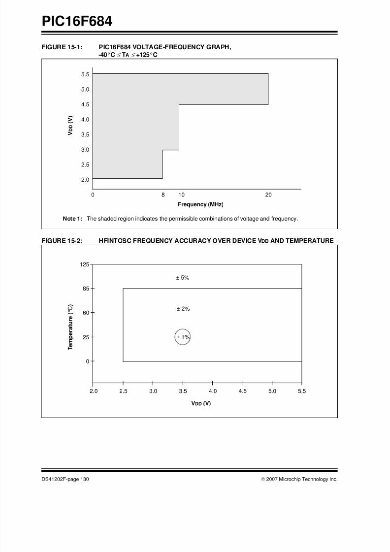
8/10/2019 PIC16F684 Datasheet
http://slidepdf.com/reader/full/pic16f684-datasheet 132/192
PIC16F684
DS41202F-page 130 © 2007 Microchip Technology Inc.
FIGURE 15-1: PIC16F684 VOLTAGE-FREQUENCY GRAPH,
-40°C ≤ TA ≤ +125°C
FIGURE 15-2: HFINTOSC FREQUENCY ACCURACY OVER DEVICE VDD AND TEMPERATURE
5.5
2.0
3.5
2.5
0
3.0
4.0
4.5
5.0
Frequency (MHz)
V D D ( V )
Note 1: The shaded region indicates the permissible combinations of voltage and frequency.
8 2010
125
25
2.0
0
60
85
VDD (V)
4.0 5.04.5
T e m p e r a
t u r e
( ° C )
2.5 3.0 3.5 5.5
± 1%
± 2%
± 5%
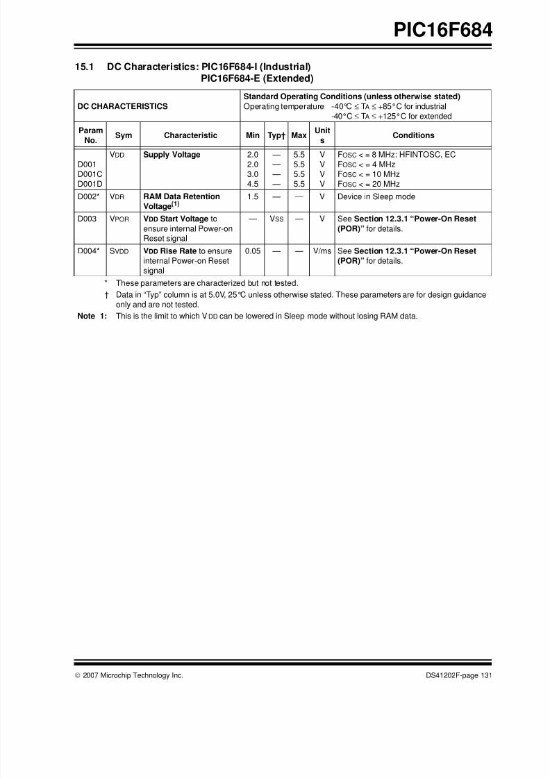
8/10/2019 PIC16F684 Datasheet
http://slidepdf.com/reader/full/pic16f684-datasheet 133/192
© 2007 Microchip Technology Inc. DS41202F-page 131
PIC16F684
15.1 DC Characteristics: PIC16F684-I (Industrial) PIC16F684-E (Extended)
DC CHARACTERISTICS
Standard Operating Conditions (unless otherwise stated)
Operating temperature -40°C ≤ TA ≤ +85°C for industrial
-40°C ≤ TA ≤ +125°C for extended
Param
No. Sym Characteristic Min Typ† MaxUnit
s Conditions
D001
D001C
D001D
VDD Supply Voltage 2.0
2.0
3.0
4.5
—
—
—
—
5.5
5.5
5.5
5.5
V
V
V
V
FOSC < = 8 MHz: HFINTOSC, EC
FOSC < = 4 MHz
FOSC < = 10 MHz
FOSC < = 20 MHz
D002* VDR RAM Data Retention
Voltage(1)1.5 — — V Device in Sleep mode
D003 VPOR VDD Start Voltage to
ensure internal Power-on
Reset signal
— VSS — V See Section 12.3.1 “Power-On Reset
(POR)” for details.
D004* SVDD VDD Rise Rate to ensure
internal Power-on Reset
signal
0.05 — — V/ms See Section 12.3.1 “Power-On Reset
(POR)” for details.
* These parameters are characterized but not tested.
† Data in “Typ” column is at 5.0V, 25°C unless otherwise stated. These parameters are for design guidance
only and are not tested.
Note 1: This is the limit to which VDD can be lowered in Sleep mode without losing RAM data.
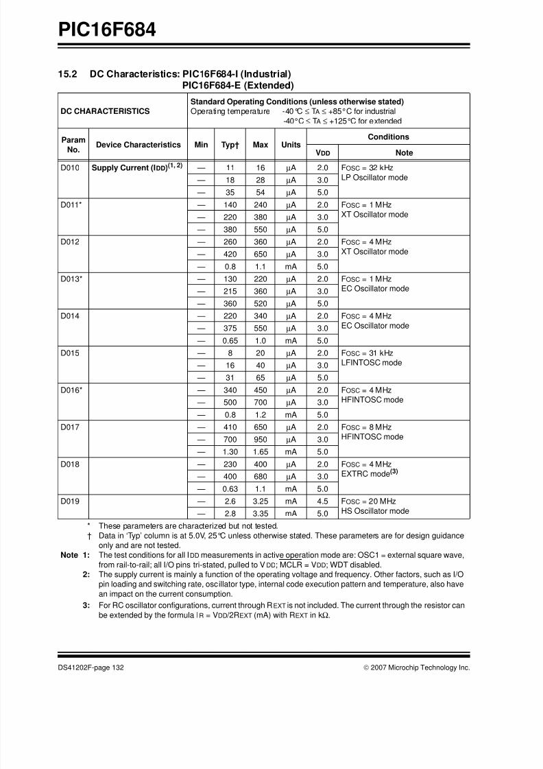
8/10/2019 PIC16F684 Datasheet
http://slidepdf.com/reader/full/pic16f684-datasheet 134/192
PIC16F684
DS41202F-page 132 © 2007 Microchip Technology Inc.
15.2 DC Characteristics: PIC16F684-I (Industrial)PIC16F684-E (Extended)
DC CHARACTERISTICS
Standard Operating Conditions (unless otherwise stated)
Operating temperature -40°C ≤ TA ≤ +85°C for industrial
-40°C ≤ TA ≤ +125°C for extended
Param
No.Device Characteristics Min Typ† Max Units
Conditions
VDD Note
D010 Supply Current (IDD)(1, 2) — 11 16 µA 2.0 FOSC = 32 kHz
LP Oscillator mode — 18 28 µA 3.0
— 35 54 µA 5.0
D011* — 140 240 µA 2.0 FOSC = 1 MHz
XT Oscillator mode — 220 380 µA 3.0
— 380 550 µA 5.0
D012 — 260 360 µA 2.0 FOSC = 4 MHz
XT Oscillator mode — 420 650 µA 3.0
— 0.8 1.1 mA 5.0D013* — 130 220 µA 2.0 FOSC = 1 MHz
EC Oscillator mode — 215 360 µA 3.0
— 360 520 µA 5.0
D014 — 220 340 µA 2.0 FOSC = 4 MHz
EC Oscillator mode — 375 550 µA 3.0
— 0.65 1.0 mA 5.0
D015 — 8 20 µA 2.0 FOSC = 31 kHz
LFINTOSC mode — 16 40 µA 3.0
— 31 65 µA 5.0
D016* — 340 450 µA 2.0 FOSC = 4 MHz
HFINTOSC mode — 500 700 µA 3.0 — 0.8 1.2 mA 5.0
D017 — 410 650 µA 2.0 FOSC = 8 MHz
HFINTOSC mode — 700 950 µA 3.0
— 1.30 1.65 mA 5.0
D018 — 230 400 µA 2.0 FOSC = 4 MHz
EXTRC mode(3) — 400 680 µA 3.0
— 0.63 1.1 mA 5.0
D019 — 2.6 3.25 mA 4.5 FOSC = 20 MHz
HS Oscillator mode — 2.8 3.35 mA 5.0
* These parameters are characterized but not tested.
† Data in ‘Typ’ column is at 5.0V, 25°C unless otherwise stated. These parameters are for design guidanceonly and are not tested.
Note 1: The test conditions for all IDD measurements in active operation mode are: OSC1 = external square wave,
from rail-to-rail; all I/O pins tri-stated, pulled to VDD; MCLR = VDD; WDT disabled.
2: The supply current is mainly a function of the operating voltage and frequency. Other factors, such as I/O
pin loading and switching rate, oscillator type, internal code execution pattern and temperature, also have
an impact on the current consumption.
3: For RC oscillator configurations, current through REXT is not included. The current through the resistor can
be extended by the formula IR = VDD /2REXT (mA) with REXT in kΩ.
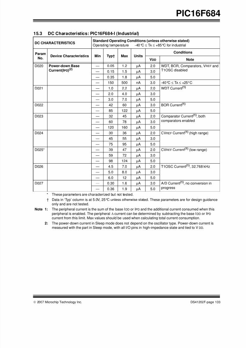
8/10/2019 PIC16F684 Datasheet
http://slidepdf.com/reader/full/pic16f684-datasheet 135/192
© 2007 Microchip Technology Inc. DS41202F-page 133
PIC16F684
15.3 DC Characteristics: PIC16F684-I (Industrial)
DC CHARACTERISTICSStandard Operating Conditions (unless otherwise stated)
Operating temperature -40°C ≤ TA ≤ +85°C for industrial
Param
No.Device Characteristics Min Typ† Max Units
Conditions
VDD NoteD020 Power-down Base
Current(IPD)(2)
— 0.05 1.2 µA 2.0 WDT, BOR, Comparators, VREF andT1OSC disabled — 0.15 1.5 µA 3.0
— 0.35 1.8 µA 5.0
— 150 500 nA 3.0 -40°C ≤ TA ≤ +25°C
D021 — 1.0 2.2 µA 2.0 WDT Current(1)
— 2.0 4.0 µA 3.0
— 3.0 7.0 µA 5.0
D022 — 42 60 µA 3.0 BOR Current(1)
— 85 122 µA 5.0
D023 — 32 45 µA 2.0 Comparator Current(1), both
comparators enabled — 60 78 µA 3.0 — 120 160 µA 5.0
D024 — 30 36 µA 2.0 CVREF Current(1) (high range)
— 45 55 µA 3.0
— 75 95 µA 5.0
D025* — 39 47 µA 2.0 CVREF Current(1) (low range)
— 59 72 µA 3.0
— 98 124 µA 5.0
D026 — 4.5 7.0 µA 2.0 T1OSC Current(1), 32.768 kHz
— 5.0 8.0 µA 3.0
— 6.0 12 µA 5.0
D027 — 0.30 1.6 µA 3.0 A/D Current(1), no conversion inprogress — 0.36 1.9 µA 5.0
* These parameters are characterized but not tested.
† Data in ‘Typ’ column is at 5.0V, 25°C unless otherwise stated. These parameters are for design guidance
only and are not tested.
Note 1: The peripheral current is the sum of the base IDD or IPD and the additional current consumed when this
peripheral is enabled. The peripheral ∆ current can be determined by subtracting the base IDD or IPD
current from this limit. Max values should be used when calculating total current consumption.
2: The power-down current in Sleep mode does not depend on the oscillator type. Power-down current is
measured with the part in Sleep mode, with all I/O pins in high-impedance state and tied to VDD.
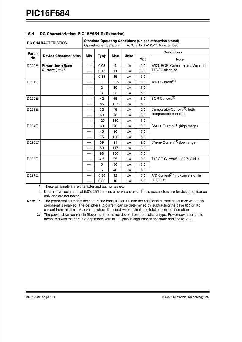
8/10/2019 PIC16F684 Datasheet
http://slidepdf.com/reader/full/pic16f684-datasheet 136/192
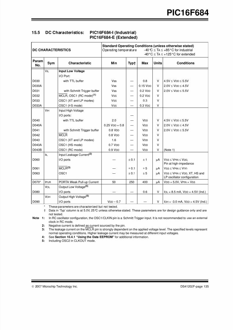
8/10/2019 PIC16F684 Datasheet
http://slidepdf.com/reader/full/pic16f684-datasheet 137/192
© 2007 Microchip Technology Inc. DS41202F-page 135
PIC16F684
15.5 DC Characteristics: PIC16F684-I (Industrial) PIC16F684-E (Extended)
DC CHARACTERISTICS
Standard Operating Conditions (unless otherwise stated)
Operating temperature -40°C ≤ TA ≤ +85°C for industrial
-40°C ≤ TA ≤ +125°C for extended
Param
No.Sym Characteristic Min Typ† Max Units Conditions
VIL Input Low Voltage
I/O Port:
D030 with TTL buffer Vss — 0.8 V 4.5V ≤ VDD ≤ 5.5V
D030A Vss — 0.15 VDD V 2.0V ≤ VDD ≤ 4.5V
D031 with Schmitt Trigger buffer Vss — 0.2 VDD V 2.0V ≤ VDD ≤ 5.5V
D032 MCLR, OSC1 (RC mode)(1) VSS — 0.2 VDD V
D033 OSC1 (XT and LP modes) VSS — 0.3 V
D033A OSC1 (HS mode) VSS — 0.3 VDD V
VIH Input High Voltage
I/O ports: —D040 with TTL buffer 2.0 — VDD V 4.5V ≤ VDD ≤ 5.5V
D040A 0.25 VDD + 0.8 — VDD V 2.0V ≤ VDD ≤ 4.5V
D041 with Schmitt Trigger buffer 0.8 VDD — VDD V 2.0V ≤ VDD ≤ 5.5V
D042 MCLR 0.8 VDD — VDD V
D043 OSC1 (XT and LP modes) 1.6 — VDD V
D043A OSC1 (HS mode) 0.7 VDD — VDD V
D043B OSC1 (RC mode) 0.9 VDD — VDD V (Note 1)
IIL Input Leakage Current(2)
D060 I/O ports — ± 0.1 ± 1 µA VSS ≤ VPIN ≤ VDD,
Pin at high-impedance
D061 MCLR(3) — ± 0.1 ± 5 µA VSS ≤ VPIN ≤ VDD
D063 OSC1 — ± 0.1 ± 5 µA VSS ≤ VPIN ≤ VDD, XT, HS andLP oscillator configuration
D070* IPUR PORTA Weak Pull-up Current 50 250 400 µA VDD = 5.0V, VPIN = VSS
VOL Output Low Voltage(5)
D080 I/O ports — — 0.6 V IOL = 8.5 mA, VDD = 4.5V (Ind.)
VOH Output High Voltage(5)
D090 I/O ports VDD – 0.7 — — V IOH = -3.0 mA, VDD = 4.5V (Ind.)
* These parameters are characterized but not tested.
† Data in ‘Typ’ column is at 5.0V, 25°C unless otherwise stated. These parameters are for design guidance only and are
not tested.
Note 1: In RC oscillator configuration, the OSC1/CLKIN pin is a Schmitt Trigger input. It is not recommended to use an external
clock in RC mode.
2: Negative current is defined as current sourced by the pin.
3: The leakage current on the MCLR pin is strongly dependent on the applied voltage level. The specified levels represent
normal operating conditions. Higher leakage current may be measured at different input voltages.
4: See Section 10.4.1 “Using the Data EEPROM” for additional information.
5: Including OSC2 in CLKOUT mode.
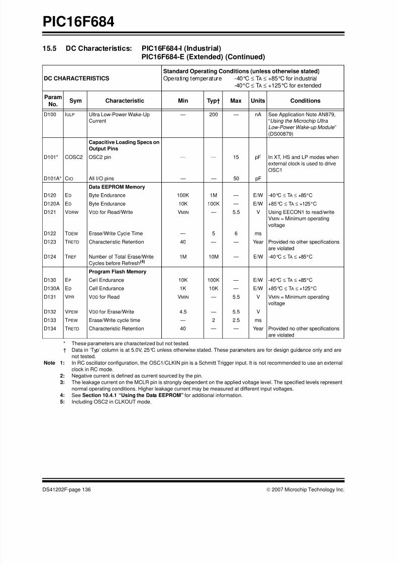
8/10/2019 PIC16F684 Datasheet
http://slidepdf.com/reader/full/pic16f684-datasheet 138/192
PIC16F684
DS41202F-page 136 © 2007 Microchip Technology Inc.
D100 IULP Ultra Low-Power Wake-Up
Current
— 200 — nA See Application Note AN879,
“Using the Microchip Ultra
Low-Power Wake-up Module ”
(DS00879)
Capacitive Loading Specs on
Output Pins
D101* COSC2 OSC2 pin — — 15 pF In XT, HS and LP modes when
external clock is used to drive
OSC1
D101A* CIO All I/O pins — — 50 pF
Data EEPROM Memory
D120 ED Byte Endurance 100K 1M — E/W -40°C ≤ TA ≤ +85°CD120A ED Byte Endurance 10K 100K — E/W +85°C ≤ TA ≤ +125°C
D121 VDRW VDD for Read/Write VMIN — 5.5 V Using EECON1 to read/write
VMIN = Minimum operating
voltage
D122 TDEW Erase/Write Cycle Time — 5 6 ms
D123 TRETD Characteristic Retention 40 — — Year Provided no other specifications
are violated
D124 TREF Number of Total Erase/Write
Cycles before Refresh(4)1M 10M — E/W -40°C ≤ TA ≤ +85°C
Program Flash Memory
D130 EP Cell Endurance 10K 100K — E/W -40°C ≤ TA ≤ +85°C
D130A ED Cell Endurance 1K 10K — E/W +85°C ≤ TA ≤ +125°C
D131 VPR VDD for Read VMIN — 5.5 V VMIN = Minimum operatingvoltage
D132 VPEW VDD for Erase/Write 4.5 — 5.5 V
D133 TPEW Erase/Write cycle time — 2 2.5 ms
D134 TRETD Characteristic Retention 40 — — Year Provided no other specifications
are violated
15.5 DC Characteristics: PIC16F684-I (Industrial) PIC16F684-E (Extended) (Continued)
DC CHARACTERISTICS
Standard Operating Conditions (unless otherwise stated)
Operating temperature -40°C ≤ TA ≤ +85°C for industrial
-40°C ≤ TA ≤ +125°C for extended
ParamNo.
Sym Characteristic Min Typ† Max Units Conditions
* These parameters are characterized but not tested.
† Data in ‘Typ’ column is at 5.0V, 25°C unless otherwise stated. These parameters are for design guidance only and are
not tested.
Note 1: In RC oscillator configuration, the OSC1/CLKIN pin is a Schmitt Trigger input. It is not recommended to use an external
clock in RC mode.
2: Negative current is defined as current sourced by the pin.
3: The leakage current on the MCLR pin is strongly dependent on the applied voltage level. The specified levels represent
normal operating conditions. Higher leakage current may be measured at different input voltages.
4: See Section 10.4.1 “Using the Data EEPROM” for additional information.5: Including OSC2 in CLKOUT mode.

8/10/2019 PIC16F684 Datasheet
http://slidepdf.com/reader/full/pic16f684-datasheet 139/192
© 2007 Microchip Technology Inc. DS41202F-page 137
PIC16F684
15.6 Thermal Considerations
Standard Operating Conditions (unless otherwise stated)
Operating temperature -40°C ≤ TA ≤ +125°C
Param
No.Sym Characteristic Typ Units Conditions
TH01 θJA Thermal ResistanceJunction to Ambient
69.8 C/W 14-pin PDIP package85.0 C/W 14-pin SOIC package
100.4 C/W 14-pin TSSOP package
46.3 C/W 16-pin QFN 4x0.9mm package
TH02 θJC Thermal Resistance
Junction to Case
32.5 C/W 14-pin PDIP package
31.0 C/W 14-pin SOIC package
31.7 C/W 14-pin TSSOP package
2.6 C/W 16-pin QFN 4x0.9mm package
TH03 TJ Junction Temperature 150 C For derated power calculations
TH04 PD Power Dissipation — W PD = PINTERNAL + PI / O
TH05 PINTERNAL Internal Power Dissipation — W PINTERNAL = IDD x VDD
(NOTE 1)
TH06 PI / O I/O Power Dissipation — W PI / O = Σ (IOL * VOL) + Σ (IOH * (VDD - VOH))TH07 PDER Derated Power — W PDER = (TJ - TA)/ θJA
(NOTE 2, 3)
Note 1: IDD is current to run the chip alone without driving any load on the output pins.
2: TA = Ambient Temperature.
3: Maximum allowable power dissipation is the lower value of either the absolute maximum total power
dissipation or derated power (PDER).
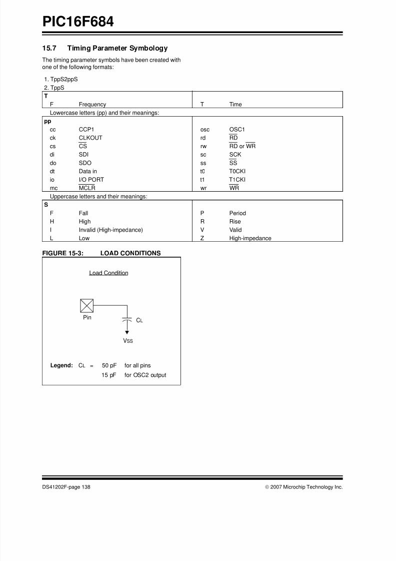
8/10/2019 PIC16F684 Datasheet
http://slidepdf.com/reader/full/pic16f684-datasheet 140/192
PIC16F684
DS41202F-page 138 © 2007 Microchip Technology Inc.
15.7 Timing Parameter Symbology
The timing parameter symbols have been created with
one of the following formats:
FIGURE 15-3: LOAD CONDITIONS
1. TppS2ppS
2. TppS
TF Frequency T Time
Lowercase letters (pp) and their meanings:
pp
cc CCP1 osc OSC1
ck CLKOUT rd RD
cs CS rw RD or WR
di SDI sc SCK
do SDO ss SS
dt Data in t0 T0CKI
io I/O PORT t1 T1CKI
mc MCLR wr WR
Uppercase letters and their meanings:S
F Fall P Period
H High R Rise
I Invalid (High-impedance) V Valid
L Low Z High-impedance
VSS
CL
Legend: CL = 50 pF for all pins
15 pF for OSC2 output
Load Condition
Pin
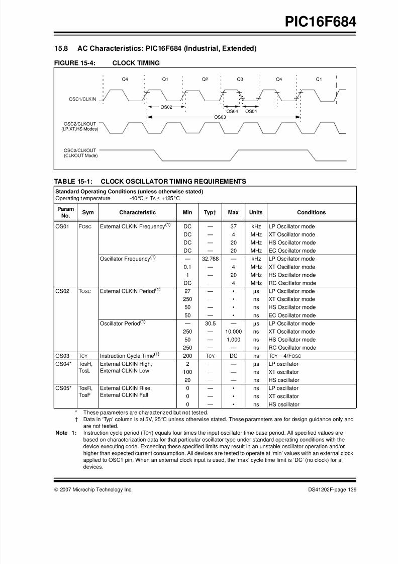
8/10/2019 PIC16F684 Datasheet
http://slidepdf.com/reader/full/pic16f684-datasheet 141/192
© 2007 Microchip Technology Inc. DS41202F-page 139
PIC16F684
15.8 AC Characteristics: PIC16F684 (Industrial, Extended)
FIGURE 15-4: CLOCK TIMING
TABLE 15-1: CLOCK OSCILLATOR TIMING REQUIREMENTS
Standard Operating Conditions (unless otherwise stated)
Operating t emperature -40°C ≤ TA ≤ +125°C
Param
No.Sym Characteristic Min Typ† Max Units Conditions
OS01 FOSC External CLKIN Frequency(1) DC — 37 kHz LP Oscillator mode
DC — 4 MHz XT Oscillator mode
DC — 20 MHz HS Oscillator mode
DC — 20 MHz EC Oscillator mode
Oscillator Frequency(1) — 32.768 — kHz LP Oscillator mode
0.1 — 4 MHz XT Oscillator mode
1 — 20 MHz HS Oscillator mode
DC — 4 MHz RC Oscillator mode
OS02 TOSC External CLKIN Period(1) 27 — • µs LP Oscillator mode
250 — • ns XT Oscillator mode
50 — • ns HS Oscillator mode
50 — • ns EC Oscillator mode
Oscillator Period(1) — 30.5 — µs LP Oscillator mode
250 — 10,000 ns XT Oscillator mode
50 — 1,000 ns HS Oscillator mode
250 — — ns RC Oscillator mode
OS03 TCY Instruction Cycle Time(1) 200 TCY DC ns TCY = 4/FOSC
OS04* TosH,
TosL
External CLKIN High,
External CLKIN Low
2 — — µs LP oscillator
100 — — ns XT oscillator
20 — — ns HS oscillator
OS05* TosR,
TosF
External CLKIN Rise,
External CLKIN Fall
0 — • ns LP oscillator
0 — • ns XT oscillator
0 — • ns HS oscillator
* These parameters are characterized but not tested.
† Data in ‘Typ’ column is at 5V, 25°C unless otherwise stated. These parameters are for design guidance only and
are not tested.
Note 1: Instruction cycle period (TCY) equals four times the input oscillator time base period. All specified values are
based on characterization data for that particular oscillator type under standard operating conditions with the
device executing code. Exceeding these specified limits may result in an unstable oscillator operation and/or
higher than expected current consumption. All devices are tested to operate at ‘min’ values with an external clock
applied to OSC1 pin. When an external clock input is used, the ‘max’ cycle time limit is ‘DC’ (no clock) for all
devices.
OSC1/CLKIN
OSC2/CLKOUT
Q4 Q1 Q2 Q3 Q4 Q1
OS02
OS03
OS04 OS04
OSC2/CLKOUT(LP,XT,HS Modes)
(CLKOUT Mode)
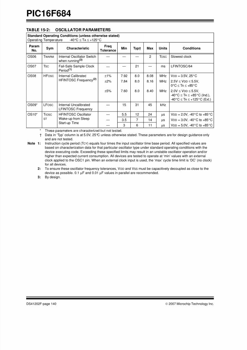
8/10/2019 PIC16F684 Datasheet
http://slidepdf.com/reader/full/pic16f684-datasheet 142/192
PIC16F684
DS41202F-page 140 © 2007 Microchip Technology Inc.
TABLE 15-2: OSCILLATOR PARAMETERS
Standard Operating Conditions (unless otherwise stated)
Operating Temperature -40°C ≤ TA ≤ +125°C
Param
No.Sym Characteristic
Freq
ToleranceMin Typ† Max Units Conditions
OS06 TWARM Internal Oscillator Switch
when running(3)
— — — 2 TOSC Slowest clock
OS07 TSC Fail-Safe Sample Clock
Period(1) — — 21 — ms LFINTOSC/64
OS08 HFOSC Internal Calibrated
HFINTOSC Frequency(2)±1% 7.92 8.0 8.08 MHz VDD = 3.5V, 25°C
±2% 7.84 8.0 8.16 MHz 2.5V ≤ VDD ≤ 5.5V,
0°C ≤ TA ≤ +85°C
±5% 7.60 8.0 8.40 MHz 2.0V ≤ VDD ≤ 5.5V,
-40°C ≤ TA ≤ +85°C (Ind.),
-40°C ≤ TA ≤ +125°C (Ext.)
OS09* LFOSC Internal Uncalibrated
LFINTOSC Frequency
— 15 31 45 kHz
OS10* TIOSC
ST
HFINTOSC Oscillator
Wake-up from Sleep
Start-up Time
— 5.5 12 24 µs VDD = 2.0V, -40°C to +85°C
— 3.5 7 14 µs VDD = 3.0V, -40°C to +85°C
— 3 6 11 µs VDD = 5.0V, -40°C to +85°C
* These parameters are characterized but not tested.
† Data in ‘Typ’ column is at 5.0V, 25°C unless otherwise stated. These parameters are for design guidance only
and are not tested.
Note 1: Instruction cycle period (TCY) equals four times the input oscillator time base period. All specified values are
based on characterization data for that particular oscillator type under standard operating conditions with the
device executing code. Exceeding these specified limits may result in an unstable oscillator operation and/or
higher than expected current consumption. All devices are tested to operate at ‘min’ values with an external
clock applied to the OSC1 pin. When an external clock input is used, the ‘max’ cycle time limit is ‘DC’ (no clock)
for all devices.
2: To ensure these oscillator frequency tolerances, VDD and VSS must be capacitively decoupled as close to the
device as possible. 0.1 µF and 0.01 µF values in parallel are recommended.
3: By design.
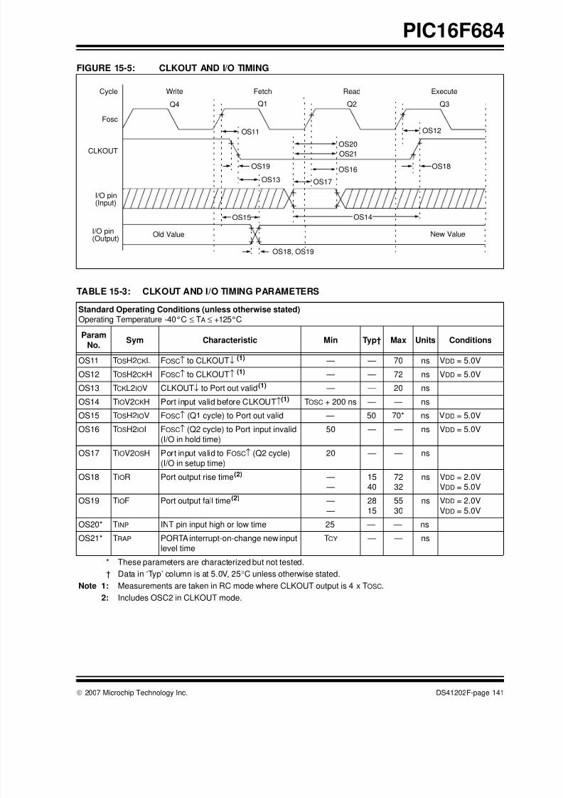
8/10/2019 PIC16F684 Datasheet
http://slidepdf.com/reader/full/pic16f684-datasheet 143/192
© 2007 Microchip Technology Inc. DS41202F-page 141
PIC16F684
FIGURE 15-5: CLKOUT AND I/O TIMING
Fosc
CLKOUT
I/O pin(Input)
I/O pin(Output)
Q4 Q1 Q2 Q3
OS11
OS19
OS13
OS15
OS18, OS19
OS20
OS21
OS17
OS16
OS14
OS12
OS18
Old Value New Value
Write Fetch Read ExecuteCycle
TABLE 15-3: CLKOUT AND I/O TIMING PARAMETERS
Standard Operating Conditions (unless otherwise stated)
Operating Temperature -40°C ≤ TA ≤ +125°C
Param
No.Sym Characteristic Min Typ† Max Units Conditions
OS11 TOSH2CKL FOSC↑ to CLKOUT↓ (1) — — 70 ns VDD = 5.0V
OS12 TOSH2CKH FOSC↑ to CLKOUT↑ (1) — — 72 ns VDD = 5.0V
OS13 TCKL2IOV CLKOUT↓ to Port out valid(1) — — 20 ns
OS14 TIOV2CKH Port input valid before CLKOUT↑(1) TOSC + 200 ns — — ns
OS15 TOSH2IOV FOSC↑ (Q1 cycle) to Port out valid — 50 70* ns VDD = 5.0VOS16 TOSH2IOI FOSC↑ (Q2 cycle) to Port input invalid
(I/O in hold time)
50 — — ns VDD = 5.0V
OS17 TIOV2OSH Port input valid to FOSC↑ (Q2 cycle)
(I/O in setup time)
20 — — ns
OS18 TIOR Port output rise time(2) —
—
15
40
72
32
ns VDD = 2.0V
VDD = 5.0V
OS19 TIOF Port output fall time(2) —
—
28
15
55
30
ns VDD = 2.0V
VDD = 5.0V
OS20* TINP INT pin input high or low time 25 — — ns
OS21* TRAP PORTA interrupt-on-change new input
level time
TCY — — ns
* These parameters are characterized but not tested.
† Data in ‘Typ’ column is at 5.0V, 25°C unless otherwise stated.
Note 1: Measurements are taken in RC mode where CLKOUT output is 4 x TOSC.
2: Includes OSC2 in CLKOUT mode.
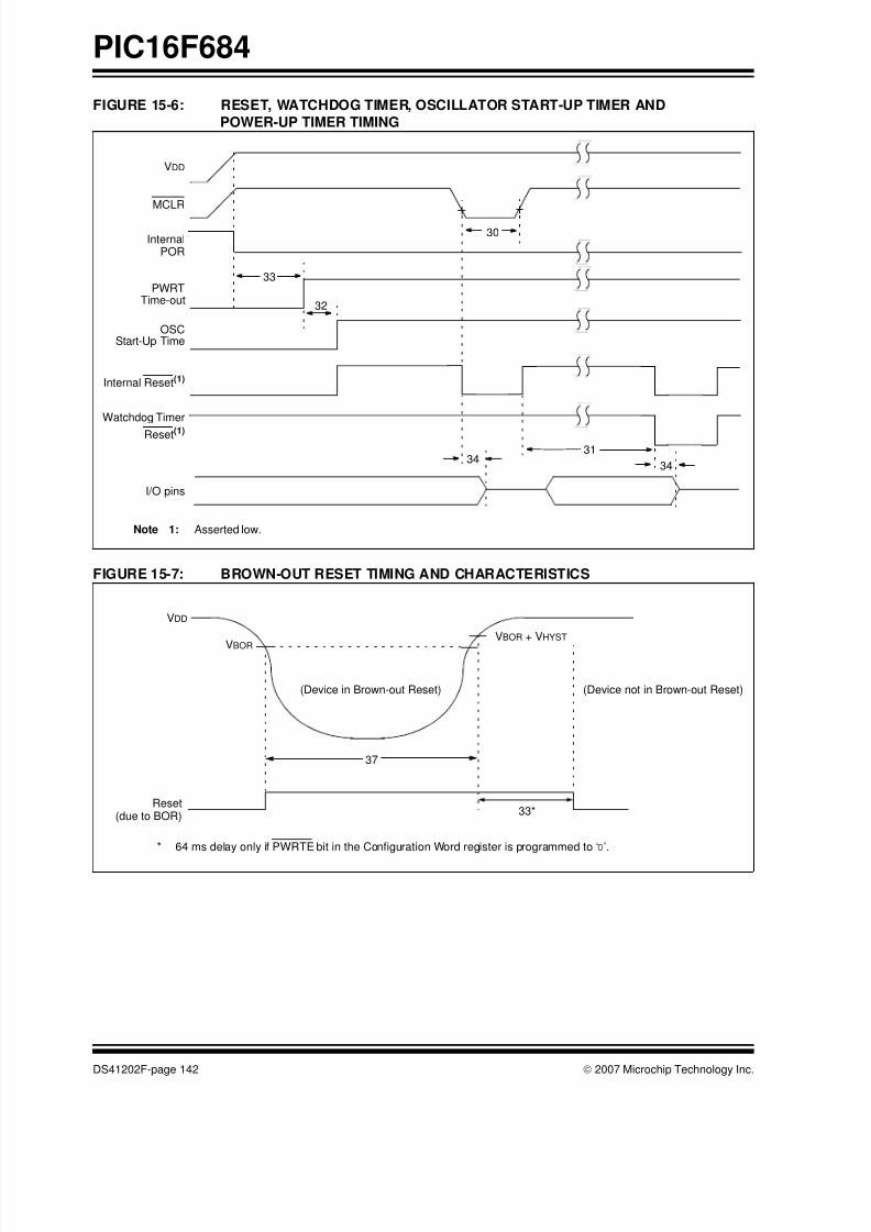
8/10/2019 PIC16F684 Datasheet
http://slidepdf.com/reader/full/pic16f684-datasheet 144/192
PIC16F684
DS41202F-page 142 © 2007 Microchip Technology Inc.
FIGURE 15-6: RESET, WATCHDOG TIMER, OSCILLATOR START-UP TIMER AND
POWER-UP TIMER TIMING
FIGURE 15-7: BROWN-OUT RESET TIMING AND CHARACTERISTICS
VDD
MCLR
InternalPOR
PWRTTime-out
OSCStart-Up Time
Internal Reset(1)
Watchdog Timer
33
32
30
3134
I/O pins
34
Note 1: Asserted low.
Reset(1)
VBOR
VDD
(Device in Brown-out Reset) (Device not in Brown-out Reset)
33*
37
* 64 ms delay only if PWRTE bit in the Configuration Word register is programmed to ‘0’.
Reset(due to BOR)
VBOR + VHYST

8/10/2019 PIC16F684 Datasheet
http://slidepdf.com/reader/full/pic16f684-datasheet 145/192
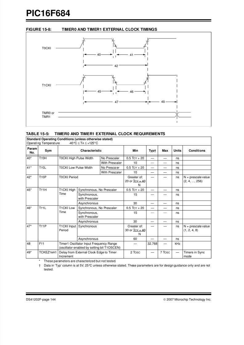
8/10/2019 PIC16F684 Datasheet
http://slidepdf.com/reader/full/pic16f684-datasheet 146/192
PIC16F684
DS41202F-page 144 © 2007 Microchip Technology Inc.
FIGURE 15-8: TIMER0 AND TIMER1 EXTERNAL CLOCK TIMINGS
TABLE 15-5: TIMER0 AND TIMER1 EXTERNAL CLOCK REQUIREMENTS
Standard Operating Conditions (unless otherwise stated)
Operating Temperature -40°C ≤ TA ≤ +125°C
Param
No.Sym Characteristic Min Typ† Max Units Conditions
40* TT0H T0CKI High Pulse Width No Prescaler 0.5 TCY + 20 — — ns
With Prescaler 10 — — ns
41* TT0L T0CKI Low Pulse Width No Prescaler 0.5 TCY + 20 — — ns
With Prescaler 10 — — ns
42* TT0P T0CKI Period Greater of:
20 or TCY + 40 N
— — ns N = prescale value
(2, 4, ..., 256)
45* TT1H T1CKI High
Time
Synchronous, No Prescaler 0.5 TCY + 20 — — ns
Synchronous,
with Prescaler
15 — — ns
Asynchronous 30 — — ns
46* TT1L T1CKI Low
Time
Synchronous, No Prescaler 0.5 TCY + 20 — — ns
Synchronous,
with Prescaler
15 — — ns
Asynchronous 30 — — ns
47* TT1P T1CKI Input
Period
Synchronous Greater of:
30 or TCY + 40
N
— — ns N = prescale value
(1, 2, 4, 8)
Asynchronous 60 — — ns
48 FT1 Timer1 Oscillator Input Frequency Range
(oscillator enabled by setting bit T1OSCEN)
— 32.768 — kHz
49* TCKEZTMR1 Delay from External Clock Edge to Timer
Increment
2 TOSC — 7 TOSC — Timers in Sync
mode
* These parameters are characterized but not tested.
† Data in ‘Typ’ column is at 5V, 25°C unless otherwise stated. These parameters are for design guidance only and are not
tested.
T0CKI
T1CKI
40 41
42
45 46
47 49
TMR0 orTMR1
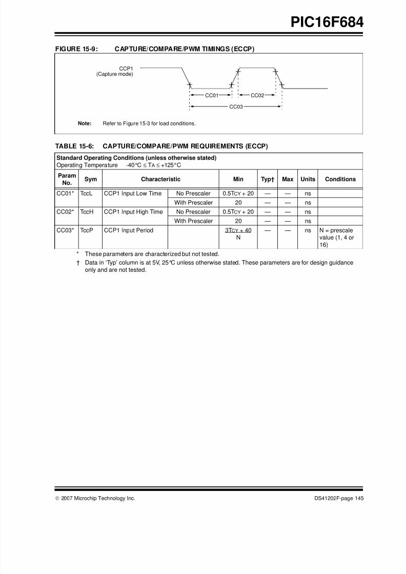
8/10/2019 PIC16F684 Datasheet
http://slidepdf.com/reader/full/pic16f684-datasheet 147/192
© 2007 Microchip Technology Inc. DS41202F-page 145
PIC16F684
FIGURE 15-9: CAPTURE/COMPARE/PWM TIMINGS (ECCP)
TABLE 15-6: CAPTURE/COMPARE/PWM REQUIREMENTS (ECCP)
Standard Operating Conditions (unless otherwise stated)
Operating Temperature -40°C ≤ TA ≤ +125°C
Param
No.Sym Characteristic Min Typ† Max Units Conditions
CC01* TccL CCP1 Input Low Time No Prescaler 0.5TCY + 20 — — ns
With Prescaler 20 — — ns
CC02* TccH CCP1 Input High Time No Prescaler 0.5TCY + 20 — — ns
With Prescaler 20 — — ns
CC03* TccP CCP1 Input Period 3TCY + 40
N
— — ns N = prescale
value (1, 4 or
16)
* These parameters are characterized but not tested.
† Data in ‘Typ’ column is at 5V, 25°C unless otherwise stated. These parameters are for design guidance
only and are not tested.
Note: Refer to Figure 15-3 for load conditions.
(Capture mode)
CC01 CC02
CC03
CCP1
8/10/2019 PIC16F684 Datasheet
http://slidepdf.com/reader/full/pic16f684-datasheet 148/192

8/10/2019 PIC16F684 Datasheet
http://slidepdf.com/reader/full/pic16f684-datasheet 149/192
© 2007 Microchip Technology Inc. DS41202F-page 147
PIC16F684
TABLE 15-9: PIC16F684 A/D CONVERTER (ADC) CHARACTERISTICS
Standard Operating Conditions (unless otherwise stated)
Operating temperature -40°C ≤ TA ≤ +125°C
Param
No.Sym Characteristic Min Typ† Max Units Conditions
AD01 NR Resolution — — 10 bits bit
AD02 EIL Integral Error — — ±1 LSb VREF = 5.12V
AD03 EDL Differential Error — — ±1 LSb No missing codes to 10 bits
VREF = 5.12V
AD04 EOFF Offset Error — — ±1 LSb VREF = 5.12V
AD07 EGN Gain Error — — ±1 LSb VREF = 5.12V
AD06
AD06A
VREF Reference Voltage(3) 2.2
2.7
— —
VDD
V
Absolute minimum to ensure 1 LSb
accuracy
AD07 VAIN Full-Scale Range VSS — VREF V
AD08 ZAIN Recommended
Impedance of Analog
Voltage Source
— — 10 kΩ
AD09* IREF VREF Input Current(3) 10 — 1000 µA During VAIN acquisition.
Based on differential of VHOLD to VAIN.
— — 50 µA During A/D conversion cycle.
* These parameters are characterized but not tested.
† Data in ‘Typ’ column is at 5.0V, 25°C unless otherwise stated. These parameters are for design guidance
only and are not tested.
Note 1: Total Absolute Error includes integral, differential, offset and gain errors.
2: The A/D conversion result never decreases with an increase in the input voltage and has no missing
codes.
3: ADC VREF is from external VREF or VDD pin, whichever is selected as reference input.
4: When ADC is off, it will not consume any current other than leakage current. The power-down current
specification includes any such leakage from the ADC module.
8/10/2019 PIC16F684 Datasheet
http://slidepdf.com/reader/full/pic16f684-datasheet 150/192
PIC16F684
DS41202F-page 148 © 2007 Microchip Technology Inc.
TABLE 15-10: PIC16F684 A/D CONVERSION REQUIREMENTS
Standard Operating Conditions (unless otherwise stated)
Operating temperature -40°C ≤ TA ≤ +125°C
Param
No.Sym Characteristic Min Typ† Max Units Conditions
AD130* TAD A/D Clock Period 1.6 — 9.0 µs TOSC-based, VREF ≥ 3.0V
3.0 — 9.0 µs TOSC-based, VREF full range
A/D Internal RC
Oscillator Period 3.0 6.0 9.0 µs
ADCS<1:0> = 11 (ADRC mode)
At VDD = 2.5V
1.6 4.0 6.0 µs At VDD = 5.0V
AD131 TCNV Conversion Time
(not including
Acquisition Time)(1)
— 11 — TAD Set GO/DONE bit to new data in A/D
Result register
AD132* TACQ Acquisition Time 11.5 — µs
AD133* TAMP Amplifier Settling Time — — 5 µs
AD134 TGO Q4 to A/D Clock Start —
—
TOSC /2
TOSC /2 + TCY
—
—
—
— If the A/D clock source is selected as
RC, a time of TCY is added before the
A/D clock starts. This allows the SLEEP
instruction to be executed.
* These parameters are characterized but not tested.
† Data in ‘Typ’ column is at 5.0V, 25°C unless otherwise stated. These parameters are for design guidance
only and are not tested.
Note 1: ADRESH and ADRESL registers may be read on the following TCY cycle.
2: See Section 9.3 “A/D Acquisition Requirements” for minimum conditions.
8/10/2019 PIC16F684 Datasheet
http://slidepdf.com/reader/full/pic16f684-datasheet 151/192

8/10/2019 PIC16F684 Datasheet
http://slidepdf.com/reader/full/pic16f684-datasheet 152/192
PIC16F684
DS41202F-page 150 © 2007 Microchip Technology Inc.
NOTES:
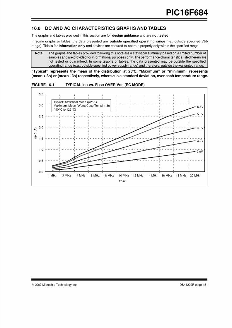
8/10/2019 PIC16F684 Datasheet
http://slidepdf.com/reader/full/pic16f684-datasheet 153/192
© 2007 Microchip Technology Inc. DS41202F-page 151
PIC16F684
16.0 DC AND AC CHARACTERISTICS GRAPHS AND TABLES
The graphs and tables provided in this section are for design guidance and are not tested.
In some graphs or tables, the data presented are outside specified operating range (i.e., outside specified VDD
range). This is for information only and devices are ensured to operate properly only within the specified range.
“Typical” represents the mean of the distribution at 25°C. “Maximum” or “minimum” represents
(mean + 3σ) or (mean - 3σ) respectively, where σ is a standard deviation, over each temperature range.
FIGURE 16-1: TYPICAL IDD vs. FOSC OVER VDD (EC MODE)
Note: The graphs and tables provided following this note are a statistical summary based on a limited number of
samples and are provided for informational purposes only. The performance characteristics listed herein arenot tested or guaranteed. In some graphs or tables, the data presented may be outside the specified
operating range (e.g., outside specified power supply range) and therefore, outside the warranted range.
3.0V
4.0V
5.0V
5.5V
2.0V
0.0
0.5
1.0
1.5
2.0
2.5
3.0
3.5
1 MHz 2 MHz 4 MHz 6 MHz 8 MHz 10 MHz 12 MHz 14 MHz 16 MHz 18 MHz 20 MHz
FOSC
I D D
( m A )
Typical: Statistical Mean @25°C
Maximum: Mean (Worst Case Temp) + 3σ(-40°C to 125°C)

8/10/2019 PIC16F684 Datasheet
http://slidepdf.com/reader/full/pic16f684-datasheet 154/192
PIC16F684
DS41202F-page 152 © 2007 Microchip Technology Inc.
FIGURE 16-2: MAXIMUM IDD vs. FOSC OVER VDD (EC MODE)
FIGURE 16-3: TYPICAL IDD vs. FOSC OVER VDD (HS MODE)
3.0V
4.0V
5.0V
2.0V
0.0
0.5
1.0
1.5
2.0
2.5
3.0
3.5
4.0
1 MHz 2 MHz 4 MHz 6 MHz 8 MHz 10 MHz 12 MHz 14 MHz 16 MHz 18 MHz 20 MHz
FOSC
I D D ( m A )
5.5V
Typical: Statistical Mean @25°C
Maximum: Mean (Worst Case Temp) + 3σ(-40°C to 125°C)
HS Mode
3.0V3.5V4.0V
4.5V
5.0V
5.5V
0.0
0.5
1.0
1.5
2.0
2.5
3.0
3.5
4.0
4 MHz 10 MHz 16 MHz 20 MHz
FOSC
I D D ( m A )
Typical: Statistical Mean @25°C
Maximum: Mean (Worst Case Temp) + 3σ(-40°C to 125°C)

8/10/2019 PIC16F684 Datasheet
http://slidepdf.com/reader/full/pic16f684-datasheet 155/192
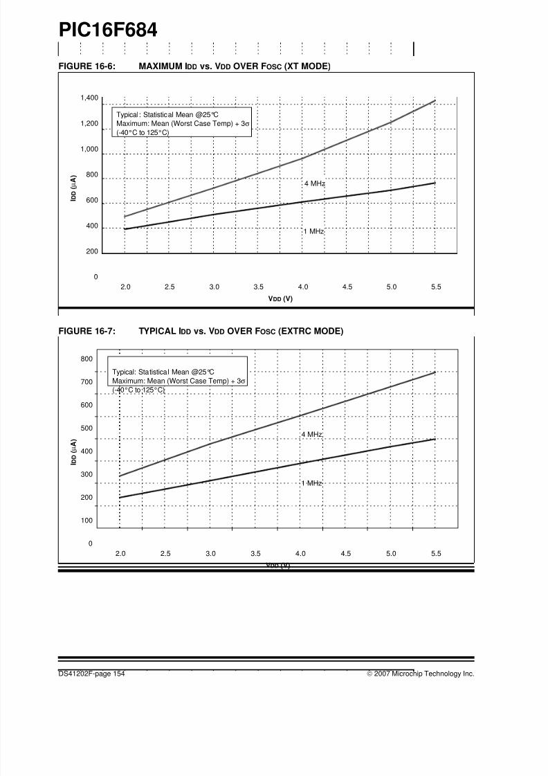
8/10/2019 PIC16F684 Datasheet
http://slidepdf.com/reader/full/pic16f684-datasheet 156/192
PIC16F684
DS41202F-page 154 © 2007 Microchip Technology Inc.
FIGURE 16-6: MAXIMUM IDD vs. VDD OVER FOSC (XT MODE)
FIGURE 16-7: TYPICAL IDD vs. VDD OVER FOSC (EXTRC MODE)
XT Mode
0
200
400
600
800
1,000
1,200
1,400
2.0 2.5 3.0 3.5 4.0 4.5 5.0 5.5
VDD (V)
I D D ( µ A )
Typical: Statistical Mean @25°C
Maximum: Mean (Worst Case Temp) + 3σ
(-40°C to 125°C)
4 MHz
1 MHz
0
100
200
300
400
500
600
700
800
2.0 2.5 3.0 3.5 4.0 4.5 5.0 5.5
VDD (V)
I D D ( µ A )
1 MHz
Typical: Statistical Mean @25°C
Maximum: Mean (Worst Case Temp) + 3σ(-40°C to 125°C)
4 MHz
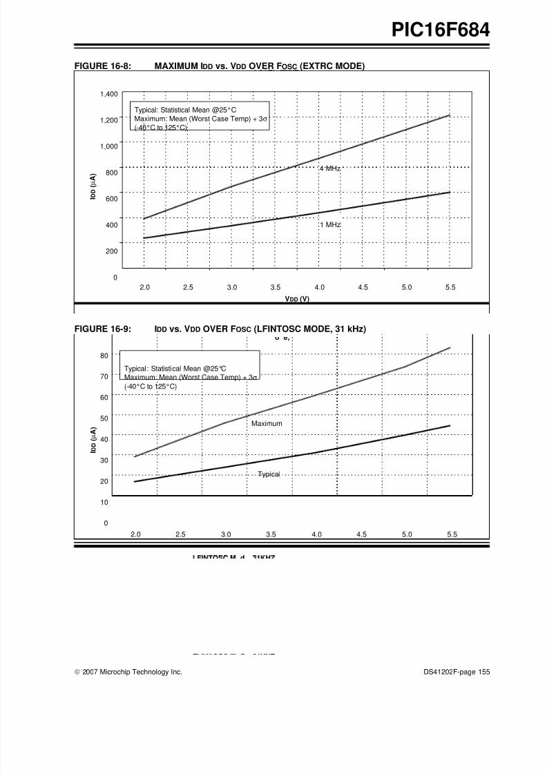
8/10/2019 PIC16F684 Datasheet
http://slidepdf.com/reader/full/pic16f684-datasheet 157/192
© 2007 Microchip Technology Inc. DS41202F-page 155
PIC16F684
FIGURE 16-8: MAXIMUM IDD vs. VDD OVER FOSC (EXTRC MODE)
FIGURE 16-9: IDD vs. VDD OVER FOSC (LFINTOSC MODE, 31 kHz)
0
200
400
600
800
1,000
1,200
1,400
2.0 2.5 3.0 3.5 4.0 4.5 5.0 5.5
VDD (V)
I D D ( µ A )
Typical: Statistical Mean @25°C
Maximum: Mean (Worst Case Temp) + 3σ(-40°C to 125°C)
4 MHz
1 MHz
o e,
Typical
Maximum
0
10
20
30
40
50
60
70
80
VDD (V)
I D D ( µ A )
Typical: Statistical Mean @25°C
Maximum: Mean (Worst Case Temp) + 3σ(-40°C to 125°C)
2.0 2.5 3.0 3.5 4.0 4.5 5.0 5.5
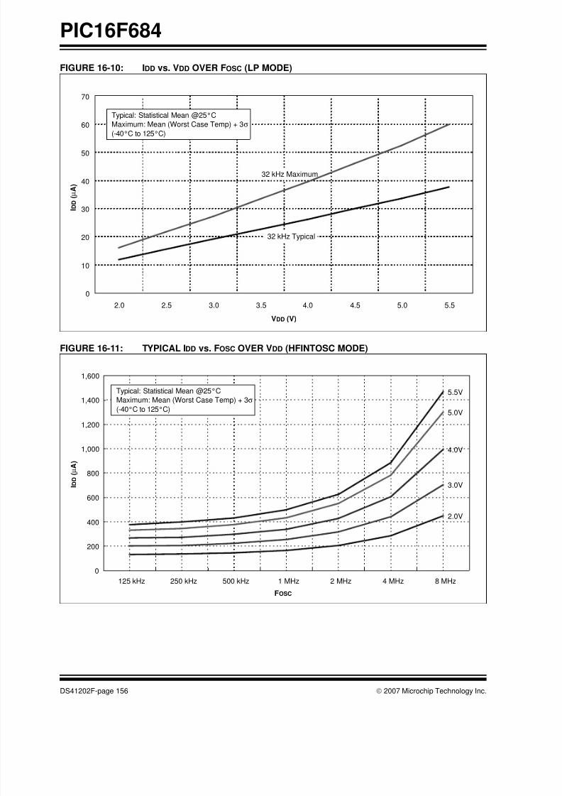
8/10/2019 PIC16F684 Datasheet
http://slidepdf.com/reader/full/pic16f684-datasheet 158/192
PIC16F684
DS41202F-page 156 © 2007 Microchip Technology Inc.
FIGURE 16-10: IDD vs. VDD OVER FOSC (LP MODE)
FIGURE 16-11: TYPICAL IDD vs. FOSC OVER VDD (HFINTOSC MODE)
0
10
20
30
40
50
60
70
2.0 2.5 3.0 3.5 4.0 4.5 5.0 5.5
VDD (V)
I D D ( µ A )
Typical: Statistical Mean @25°C
Maximum: Mean (Worst Case Temp) + 3σ(-40°C to 125°C)
32 kHz Maximum
32 kHz Typical
2.0V
3.0V
4.0V
5.0V
5.5V
0
200
400
600
800
1,000
1,200
1,400
1,600
125 kHz 250 kHz 500 kHz 1 MHz 2 MHz 4 MHz 8 MHz
FOSC
I D D ( µ A )
Typical: Statistical Mean @25°C
Maximum: Mean (Worst Case Temp) + 3σ(-40°C to 125°C)
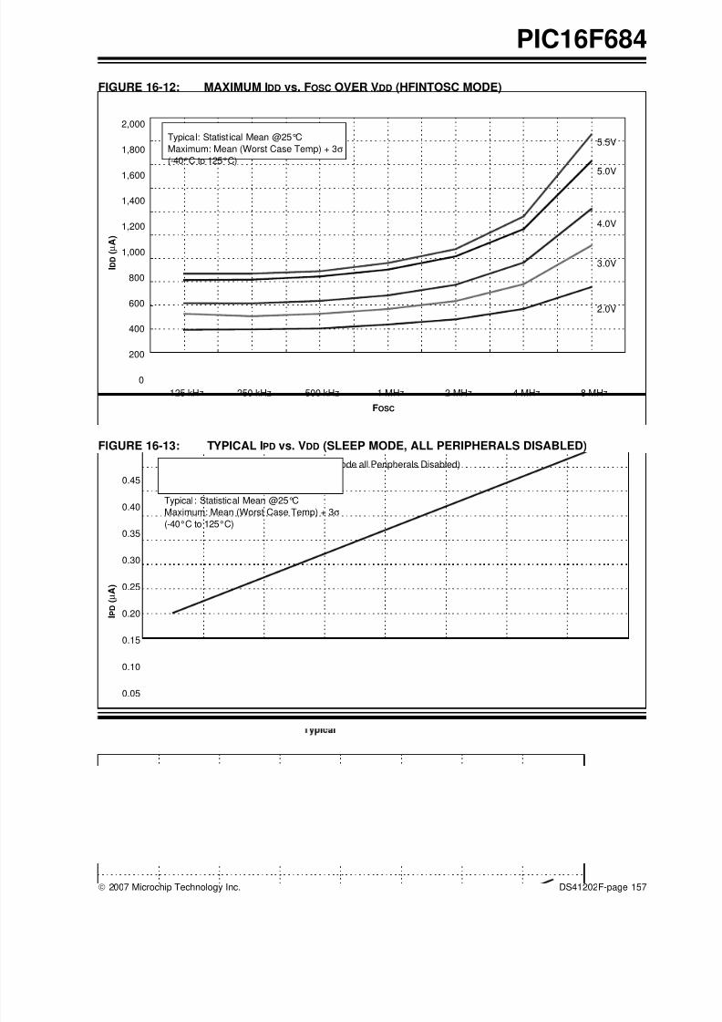
8/10/2019 PIC16F684 Datasheet
http://slidepdf.com/reader/full/pic16f684-datasheet 159/192
© 2007 Microchip Technology Inc. DS41202F-page 157
PIC16F684
FIGURE 16-12: MAXIMUM IDD vs. FOSC OVER VDD (HFINTOSC MODE)
FIGURE 16-13: TYPICAL IPD vs. VDD (SLEEP MODE, ALL PERIPHERALS DISABLED)
2.0V
3.0V
4.0V
5.0V
5.5V
0
200
400
600
800
1,000
1,200
1,400
1,600
1,800
2,000
125 kHz 250 kHz 500 kHz 1 MHz 2 MHz 4 MHz 8 MHz
FOSC
I D D ( µ A )
Typical: Statistical Mean @25°C
Maximum: Mean (Worst Case Temp) + 3σ(-40°C to 125°C)
(Sleep Mode all Peripherals Disabled)
0.0
0.05
0.10
0.15
0.20
0.25
0.30
0.35
0.40
0.45
2.0 2.5 3.0 3.5 4.0 4.5 5.0 5.5
VDD (V)
I P D ( µ A )
Typical: Statistical Mean @25°C
Maximum: Mean (Worst Case Temp) + 3σ(-40°C to 125°C)
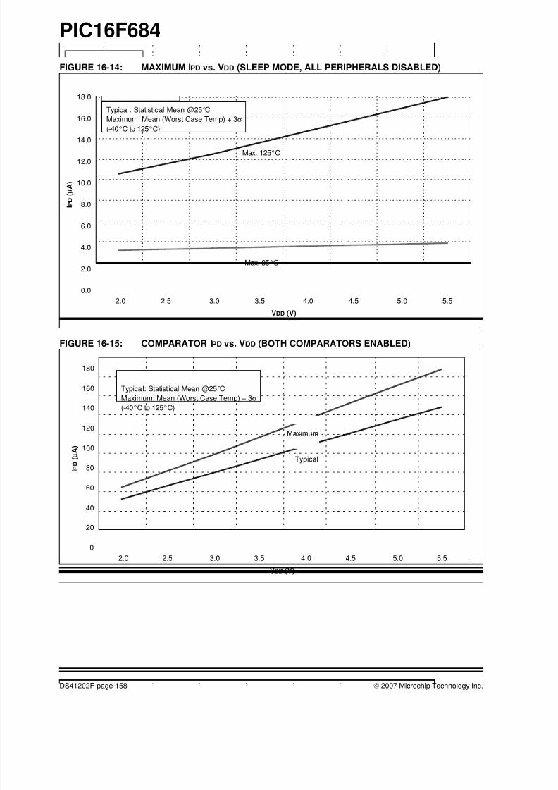
8/10/2019 PIC16F684 Datasheet
http://slidepdf.com/reader/full/pic16f684-datasheet 160/192
PIC16F684
DS41202F-page 158 © 2007 Microchip Technology Inc.
FIGURE 16-14: MAXIMUM IPD vs. VDD (SLEEP MODE, ALL PERIPHERALS DISABLED)
FIGURE 16-15: COMPARATOR IPD vs. VDD (BOTH COMPARATORS ENABLED)
Maximum(Sleep Mode all Peripherals Disabled)
Max. 125°C
Max. 85°C
0.0
2.0
4.0
6.0
8.0
10.0
12.0
14.0
16.0
18.0
2.0 2.5 3.0 3.5 4.0 4.5 5.0 5.5
VDD (V)
I P D
( µ A )
Maximum: Mean + 3σTypical: Statistical Mean @25°C
Maximum: Mean (Worst Case Temp) + 3σ(-40°C to 125°C)
0
20
40
60
80
100
120
140
160
180
2.0 2.5 3.0 3.5 4.0 4.5 5.0 5.5
VDD (V)
I P D
( µ A )
Maximum
Typical
Typical: Statistical Mean @25°C
Maximum: Mean (Worst Case Temp) + 3σ(-40°C to 125°C)
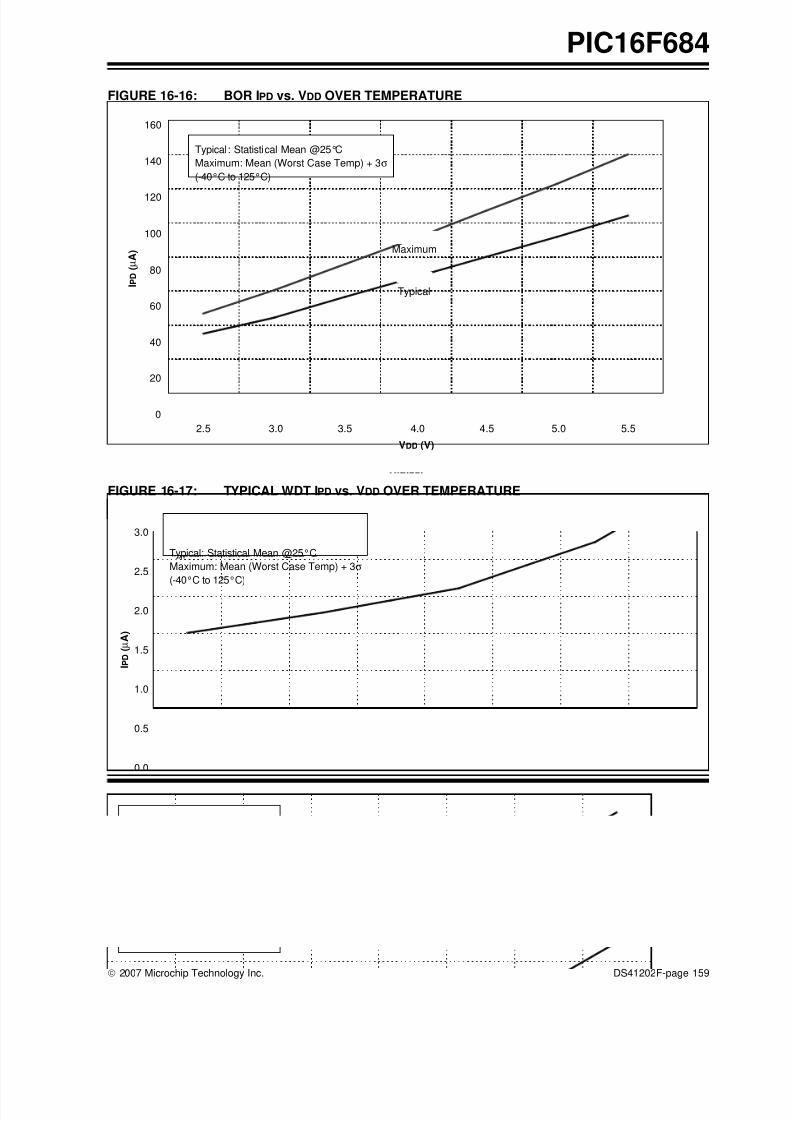
8/10/2019 PIC16F684 Datasheet
http://slidepdf.com/reader/full/pic16f684-datasheet 161/192
© 2007 Microchip Technology Inc. DS41202F-page 159
PIC16F684
FIGURE 16-16: BOR IPD vs. VDD OVER TEMPERATURE
FIGURE 16-17: TYPICAL WDT IPD vs. VDD OVER TEMPERATURE
0
20
40
60
80
100
120
140
160
2.5 3.0 3.5 4.0 4.5 5.0 5.5
VDD (V)
I P D ( µ A )
Typical: Statistical Mean @25°C
Maximum: Mean (Worst Case Temp) + 3σ(-40°C to 125°C)
Maximum
Typical
0.0
0.5
1.0
1.5
2.0
2.5
3.0
2.0 2.5 3.0 3.5 4.0 4.5 5.0 5.5VDD (V)
I P D
( µ A )
Typical: Statistical Mean @25°CTypical: Statistical Mean @25°C
Maximum: Mean (Worst Case Temp) + 3σ(-40°C to 125°C)
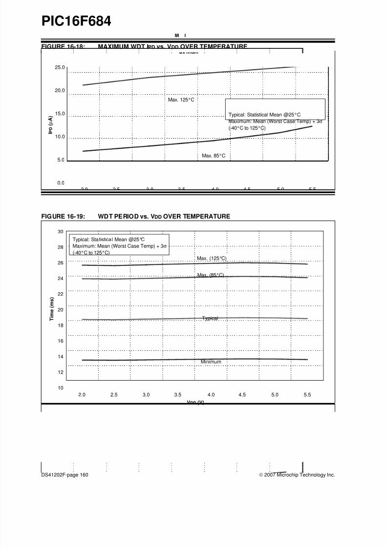
8/10/2019 PIC16F684 Datasheet
http://slidepdf.com/reader/full/pic16f684-datasheet 162/192
PIC16F684
DS41202F-page 160 © 2007 Microchip Technology Inc.
FIGURE 16-18: MAXIMUM WDT IPD vs. VDD OVER TEMPERATURE
FIGURE 16-19: WDT PERIOD vs. VDD OVER TEMPERATURE
ax mum
Max. 125°C
Max. 85°C
0.0
5.0
10.0
15.0
20.0
25.0
2.0 2.5 3.0 3.5 4.0 4.5 5.0 5.5VDD (V)
I P D ( µ A ) Typical: Statistical Mean @25°C
Maximum: Mean (Worst Case Temp) + 3σ(-40°C to 125°C)
Minimum
Typical
10
12
14
16
18
20
22
24
26
28
30
2.0 2.5 3.0 3.5 4.0 4.5 5.0 5.5
VDD (V)
T i m e ( m s )
Typical: Statistical Mean @25°C
Maximum: Mean (Worst Case Temp) + 3σ(-40°C to 125°C)
Max. (125°C)
Max. (85°C)
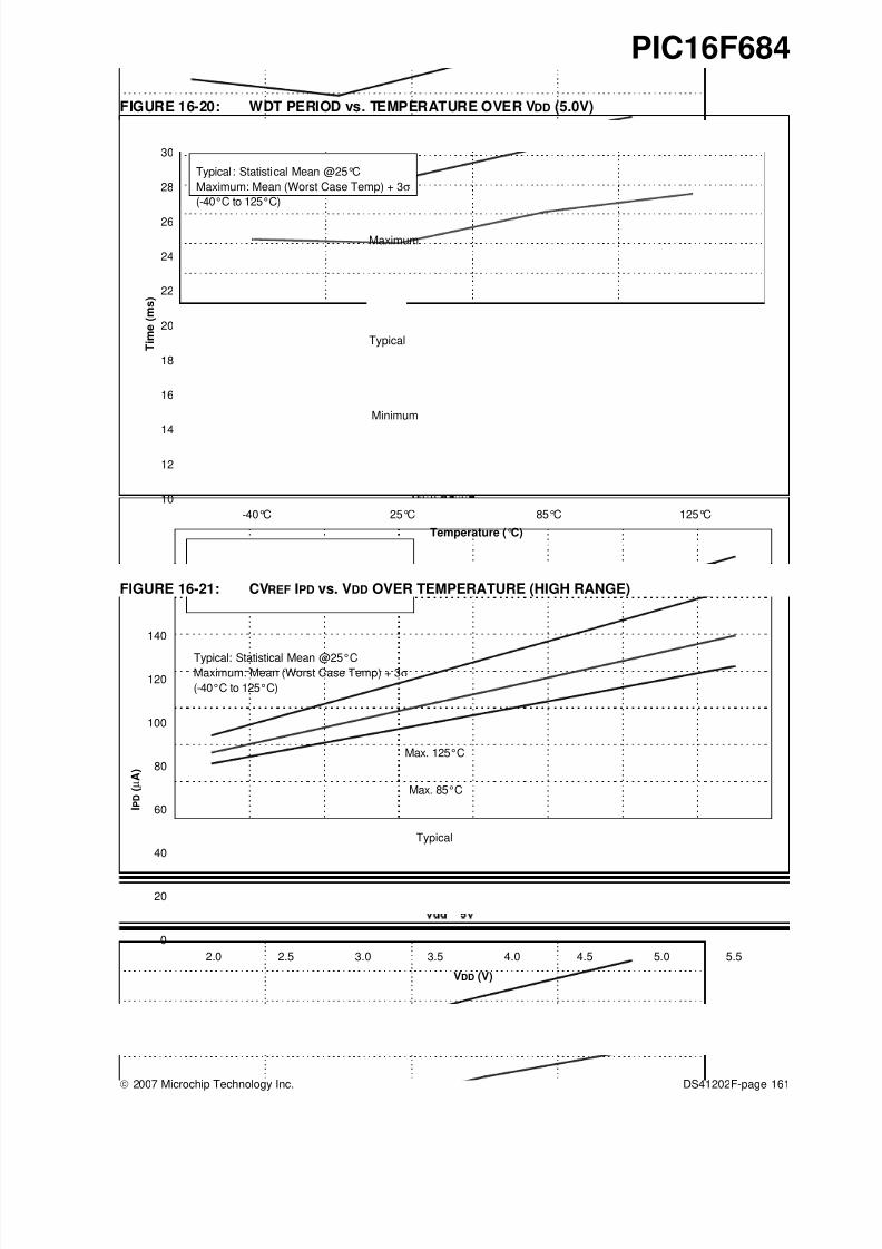
8/10/2019 PIC16F684 Datasheet
http://slidepdf.com/reader/full/pic16f684-datasheet 163/192
© 2007 Microchip Technology Inc. DS41202F-page 161
PIC16F684
FIGURE 16-20: WDT PERIOD vs. TEMPERATURE OVER VDD (5.0V)
FIGURE 16-21: CVREF IPD vs. VDD OVER TEMPERATURE (HIGH RANGE)
=
10
12
14
16
18
20
22
24
26
28
30
-40°C 25°C 85°C 125°C
Temperature (°C)
T i m e ( m s )
Typical: Statistical Mean @25°C
Maximum: Mean (Worst Case Temp) + 3σ(-40°C to 125°C)
Maximum
Typical
Minimum
Typical
Max. 85°C
0
20
40
60
80
100
120
140
2.0 2.5 3.0 3.5 4.0 4.5 5.0 5.5
VDD (V)
I P D ( µ A )
Max. 125°C
Typical: Statistical Mean @25°CMaximum: Mean (Worst Case Temp) + 3σ(-40°C to 125°C)
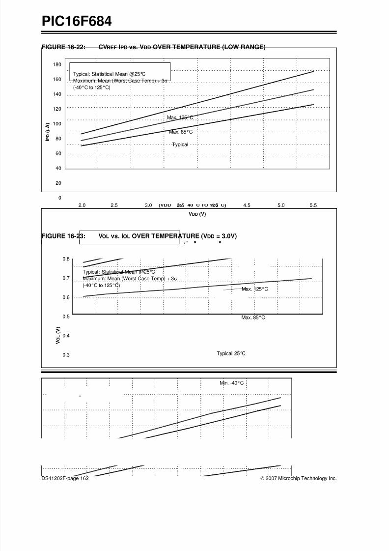
8/10/2019 PIC16F684 Datasheet
http://slidepdf.com/reader/full/pic16f684-datasheet 164/192
PIC16F684
DS41202F-page 162 © 2007 Microchip Technology Inc.
FIGURE 16-22: CVREF IPD vs. VDD OVER TEMPERATURE (LOW RANGE)
FIGURE 16-23: VOL vs. IOL OVER TEMPERATURE (VDD = 3.0V)
Typical
Max. 85°C
0
20
40
60
80
100
120
140
160
180
2.0 2.5 3.0 3.5 4.0 4.5 5.0 5.5
VDD (V)
I P D ( µ A )
Max. 125°C
Typical: Statistical Mean @25°C
Maximum: Mean (Worst Case Temp) + 3σ(-40°C to 125°C)
= , - × ×
0.0
0.1
0.2
0.3
0.4
0.5
0.6
0.7
0.8
5.0 5.5 6.0 6.5 7.0 7.5 8.0 8.5 9.0 9.5 10.0
IOL (mA)
V O L ( V )
Max. 85°C
Max. 125°C
Typical 25°C
Min. -40°C
Typical: Statistical Mean @25°C
Maximum: Mean (Worst Case Temp) + 3σ(-40°C to 125°C)
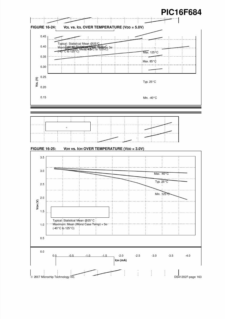
8/10/2019 PIC16F684 Datasheet
http://slidepdf.com/reader/full/pic16f684-datasheet 165/192
© 2007 Microchip Technology Inc. DS41202F-page 163
PIC16F684
FIGURE 16-24: VOL vs. IOL OVER TEMPERATURE (VDD = 5.0V)
FIGURE 16-25: VOH vs. IOH OVER TEMPERATURE (VDD = 3.0V)
0.00
0.05
0.10
0.15
0.20
0.25
0.30
0.35
0.40
0.45
5.0 5.5 6.0 6.5 7.0 7.5 8.0 8.5 9.0 9.5 10.0
IOL (mA)
V O L ( V )
Typical: Statistical Mean @25×CMaximum: Meas + 3(-40×C to 125×C)
Typical: Statistical Mean @25°C
Maximum: Mean (Worst Case Temp) + 3σ(-40°C to 125°C)
Max. 85°C
Typ. 25°C
Min. -40°C
Max. 125°C
0.0
0.5
1.0
1.5
2.0
2.5
3.0
3.5
-4.0-3.5-3.0-2.5-2.0-1.5-1.0-0.50.0
IOH (mA)
V O H ( V )
Typ. 25°C
Max. -40°C
Min. 125°C
Typical: Statistical Mean @25°C
Maximum: Mean (Worst Case Temp) + 3σ(-40°C to 125°C)
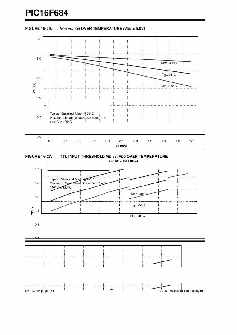
8/10/2019 PIC16F684 Datasheet
http://slidepdf.com/reader/full/pic16f684-datasheet 166/192
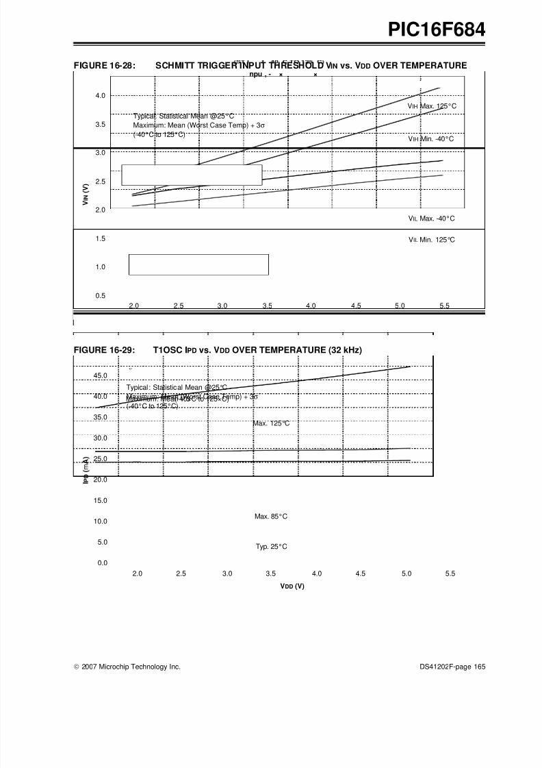
8/10/2019 PIC16F684 Datasheet
http://slidepdf.com/reader/full/pic16f684-datasheet 167/192
© 2007 Microchip Technology Inc. DS41202F-page 165
PIC16F684
FIGURE 16-28: SCHMITT TRIGGER INPUT THRESHOLD VIN vs. VDD OVER TEMPERATURE
FIGURE 16-29: T1OSC IPD vs. VDD OVER TEMPERATURE (32 kHz)
npu , - × ×
0.5
1.0
1.5
2.0
2.5
3.0
3.5
4.0
2.0 2.5 3.0 3.5 4.0 4.5 5.0 5.5
VDD (V)
V I N
( V )
VIH Max. 125°C
VIH Min. -40°C
VIL Min. 125°C
VIL Max. -40°C
Typical: Statistical Mean @25°C
Maximum: Mean (Worst Case Temp) + 3σ
(-40°C to 125°C)
Typ. 25°C
Max. 85°C
Max. 125°C
0.0
5.0
10.0
15.0
20.0
25.0
30.0
35.0
40.0
45.0
2.0 2.5 3.0 3.5 4.0 4.5 5.0 5.5
VDD (V)
I P D ( m A )
Maximum: Mean + 3(-40×C to 125×C)
Typical: Statistical Mean @25°C
Maximum: Mean (Worst Case Temp) + 3σ
(-40°C to 125°C)

8/10/2019 PIC16F684 Datasheet
http://slidepdf.com/reader/full/pic16f684-datasheet 168/192
PIC16F684
DS41202F-page 166 © 2007 Microchip Technology Inc.
FIGURE 16-30: COMPARATOR RESPONSE TIME (RISING EDGE)
FIGURE 16-31: COMPARATOR RESPONSE TIME (FALLING EDGE)
0
100
200
300
400
500
600
700
800
900
1000
2.0 2.5 4.0 5.5
VDD (V)
R e s p o n s e T i m e ( n S )
Max. 85°C
Typ. 25°C
Min. -40°C
Max. 125°C
Note:
V- input = Transition from VCM + 100MV to VCM - 20MV
V+ input = VCM
VCM = VDD - 1.5V)/2
0
100
200
300
400
500
600
700
800
900
1000
2.0 2.5 4.0 5.5
VDD (V)
R e s p o n s e T i m e ( n S )
Max. 85°C
Typ. 25°C
Min. -40°C
Max. 125°C
Note:
V- input = Transition from VCM - 100MV to VCM + 20MV
V+ input = VCM
VCM = VDD - 1.5V)/2
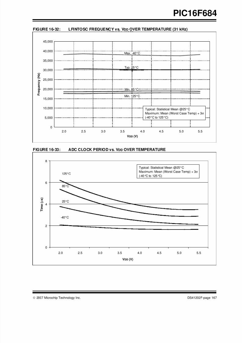
8/10/2019 PIC16F684 Datasheet
http://slidepdf.com/reader/full/pic16f684-datasheet 169/192
© 2007 Microchip Technology Inc. DS41202F-page 167
PIC16F684
FIGURE 16-32: LFINTOSC FREQUENCY vs. VDD OVER TEMPERATURE (31 kHz)
FIGURE 16-33: ADC CLOCK PERIOD vs. VDD OVER TEMPERATURE
0
5,000
10,000
15,000
20,000
25,000
30,000
35,000
40,000
45,000
2.0 2.5 3.0 3.5 4.0 4.5 5.0 5.5
VDD (V)
F r e q u e n c y ( H z )
Max. -40°C
Typ. 25°C
Min. 85°C
Min. 125°C
Typical: Statistical Mean @25°C
Maximum: Mean (Worst Case Temp) + 3σ(-40°C to 125°C)
0
2
4
6
8
2.0 2.5 3.0 3.5 4.0 4.5 5.0 5.5
VDD (V)
T i m e ( µ s )
25°C
85°C
125°C
-40°C
Typical: Statistical Mean @25°C
Maximum: Mean (Worst Case Temp) + 3σ(-40°C to 125°C)

8/10/2019 PIC16F684 Datasheet
http://slidepdf.com/reader/full/pic16f684-datasheet 170/192
PIC16F684
DS41202F-page 168 © 2007 Microchip Technology Inc.
FIGURE 16-34: TYPICAL HFINTOSC START-UP TIMES vs. VDD OVER TEMPERATURE
FIGURE 16-35: MAXIMUM HFINTOSC START-UP TIMES vs. VDD OVER TEMPERATURE
0
2
4
6
8
10
12
14
16
2.0 2.5 3.0 3.5 4.0 4.5 5.0 5.5
VDD (V)
T i m e ( µ s )
85°C
25°C
-40°C
Typical: Statistical Mean @25°C
Maximum: Mean (Worst Case Temp) + 3σ(-40°C to 125°C)
-
0
5
10
15
20
25
2.0 2.5 3.0 3.5 4.0 4.5 5.0 5.5
VDD (V)
T i m e ( µ s )
-40°C
85°C
25°C
Typical: Statistical Mean @25°C
Maximum: Mean (Worst Case Temp) + 3σ(-40°C to 125°C)
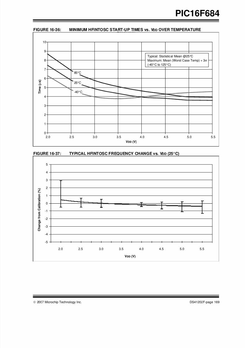
8/10/2019 PIC16F684 Datasheet
http://slidepdf.com/reader/full/pic16f684-datasheet 171/192
© 2007 Microchip Technology Inc. DS41202F-page 169
PIC16F684
FIGURE 16-36: MINIMUM HFINTOSC START-UP TIMES vs. VDD OVER TEMPERATURE
FIGURE 16-37: TYPICAL HFINTOSC FREQUENCY CHANGE vs. VDD (25°C)
0
1
2
3
4
5
6
7
8
9
10
2.0 2.5 3.0 3.5 4.0 4.5 5.0 5.5
VDD (V)
T i m e ( µ s )
-40°C
25°C
85°C
Typical: Statistical Mean @25°C
Maximum: Mean (Worst Case Temp) + 3σ(-40°C to 125°C)
-5
-4
-3
-2
-1
0
1
2
3
4
5
2.0 2.5 3.0 3.5 4.0 4.5 5.0 5.5
VDD (V)
C h a n g e f r o m C
a l i b r a t i o n ( % )
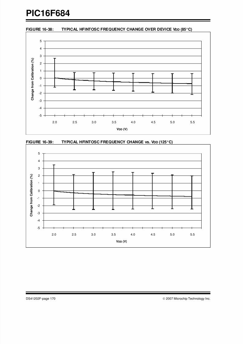
8/10/2019 PIC16F684 Datasheet
http://slidepdf.com/reader/full/pic16f684-datasheet 172/192
PIC16F684
DS41202F-page 170 © 2007 Microchip Technology Inc.
FIGURE 16-38: TYPICAL HFINTOSC FREQUENCY CHANGE OVER DEVICE VDD (85°C)
FIGURE 16-39: TYPICAL HFINTOSC FREQUENCY CHANGE vs. VDD (125°C)
-5
-4
-3
-2
-1
0
1
2
3
4
5
2.0 2.5 3.0 3.5 4.0 4.5 5.0 5.5
VDD (V)
C h a n g e f r o m C
a l i b r a t i o n ( %
)
-5
-4
-3
-2
-1
0
1
2
3
4
5
2.0 2.5 3.0 3.5 4.0 4.5 5.0 5.5
VDD (V)
C h a n g e f r o m C
a l i b r a t i o n
( % )
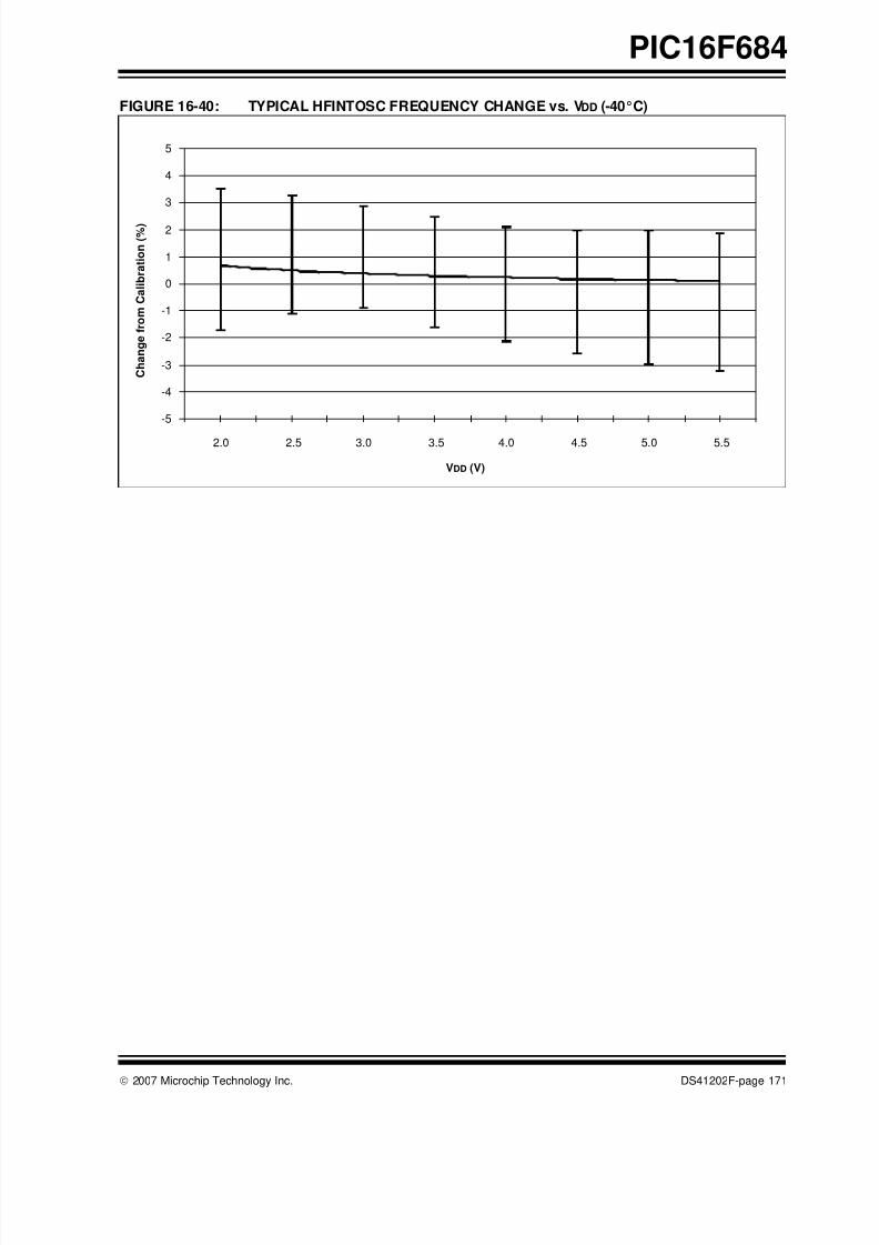
8/10/2019 PIC16F684 Datasheet
http://slidepdf.com/reader/full/pic16f684-datasheet 173/192
© 2007 Microchip Technology Inc. DS41202F-page 171
PIC16F684
FIGURE 16-40: TYPICAL HFINTOSC FREQUENCY CHANGE vs. VDD (-40°C)
-5
-4
-3
-2
-1
0
1
2
3
4
5
2.0 2.5 3.0 3.5 4.0 4.5 5.0 5.5
VDD (V)
C h a n g e f r o m C
a l i b r a t i o n ( % )

8/10/2019 PIC16F684 Datasheet
http://slidepdf.com/reader/full/pic16f684-datasheet 174/192
PIC16F684
DS41202F-page 172 © 2007 Microchip Technology Inc.
NOTES:
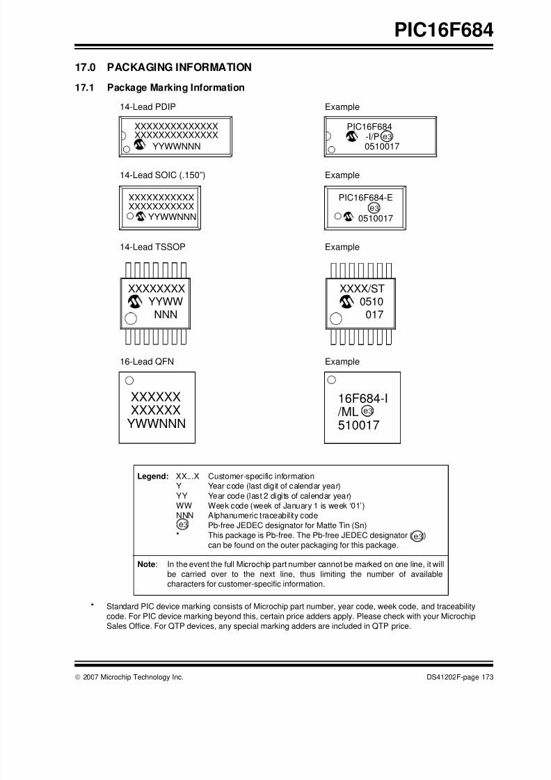
8/10/2019 PIC16F684 Datasheet
http://slidepdf.com/reader/full/pic16f684-datasheet 175/192
© 2007 Microchip Technology Inc. DS41202F-page 173
PIC16F684
17.0 PACKAGING INFORMATION
17.1 Package Marking Information
* Standard PIC device marking consists of Microchip part number, year code, week code, and traceability
code. For PIC device marking beyond this, certain price adders apply. Please check with your Microchip
Sales Office. For QTP devices, any special marking adders are included in QTP price.
XXXXXX
16-Lead QFN
XXXXXXYWWNNN
16F684-I
Example
/ML510017
14-Lead PDIP
XXXXXXXXXXXXXX
XXXXXXXXXXXXXXYYWWNNN
Example
PIC16F684
0510017
14-Lead SOIC (.150”)
XXXXXXXXXXXXXXXXXXXXXX
YYWWNNN
Example
PIC16F684-E
0510017
14-Lead TSSOP
XXXXXXXXYYWWNNN
Example
XXXX/ST0510017
Legend: XX...X Customer-specific information
Y Year code (last digit of calendar year)
YY Year code (last 2 digits of calendar year)
WW Week code (week of January 1 is week ‘01’)
NNN Alphanumeric traceability code
Pb-free JEDEC designator for Matte Tin (Sn)
* This package is Pb-free. The Pb-free JEDEC designator ( )
can be found on the outer packaging for this package.
Note: In the event the full Microchip part number cannot be marked on one line, it will
be carried over to the next line, thus limiting the number of available
characters for customer-specific information.
3e
3e
3e
3e
3e
-I/P
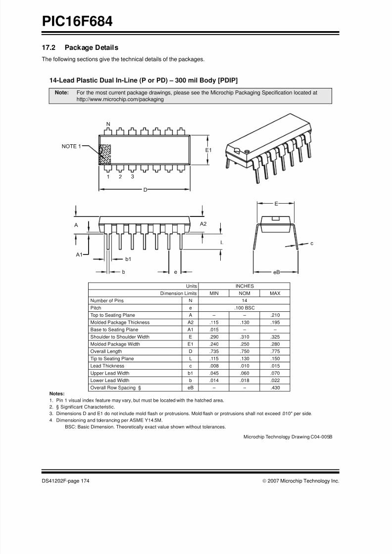
8/10/2019 PIC16F684 Datasheet
http://slidepdf.com/reader/full/pic16f684-datasheet 176/192
PIC16F684
DS41202F-page 174 © 2007 Microchip Technology Inc.
17.2 Package Details
The following sections give the technical details of the packages.
14-Lead Plastic Dual In-Line (P or PD) – 300 mil Body [PDIP]
Notes:
1. Pin 1 visual index feature may vary, but must be located with the hatched area.
2. § Significant Characteristic.
3. Dimensions D and E1 do not include mold flash or protrusions. Mold flash or protrusions shall not exceed .010" per side.
4. Dimensioning and tolerancing per ASME Y14.5M.
BSC: Basic Dimension. Theoretically exact value shown without tolerances.
Note: For the most current package drawings, please see the Microchip Packaging Specification located at
http://www.microchip.com/packaging
Units INCHES
Dimension Limits MIN NOM MAX
Number of Pins N 14
Pitch e .100 BSC
Top to Seating Plane A – – .210
Molded Package Thickness A2 .115 .130 .195
Base to Seating Plane A1 .015 – –
Shoulder to Shoulder Width E .290 .310 .325
Molded Package Width E1 .240 .250 .280
Overall Length D .735 .750 .775
Tip to Seating Plane L .115 .130 .150
Lead Thickness c .008 .010 .015
Upper Lead Width b1 .045 .060 .070
Lower Lead Width b .014 .018 .022
Overall Row Spacing § eB – – .430
N
E1
D
NOTE 1
1 2 3
E
c
eB
A2
L
A
A1b1
b e
Microchip Technology Drawing C04-005B
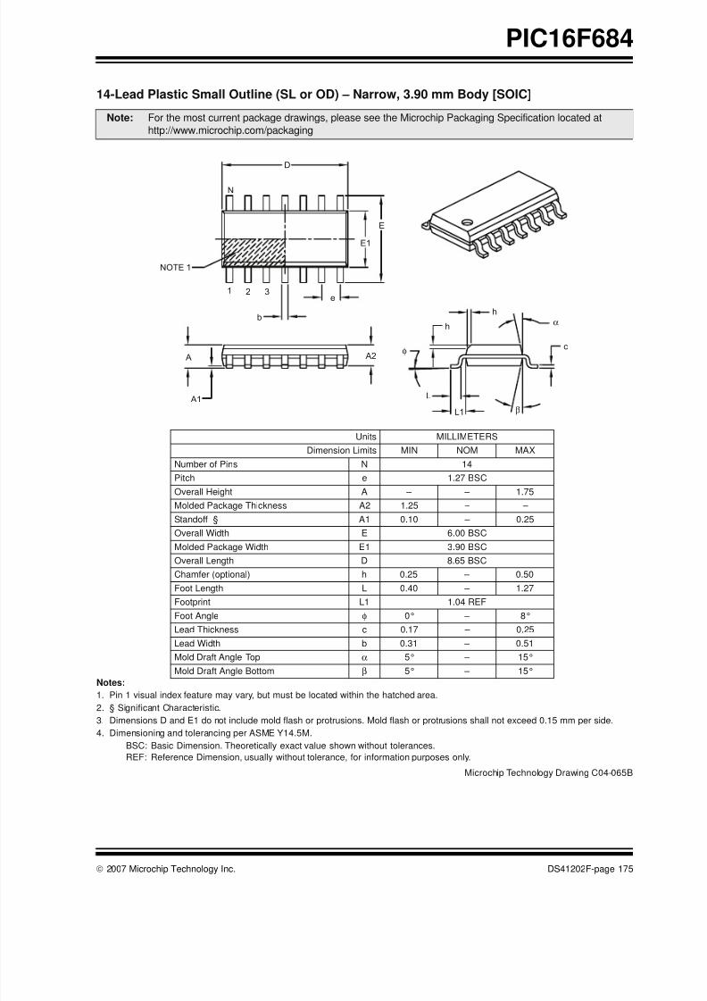
8/10/2019 PIC16F684 Datasheet
http://slidepdf.com/reader/full/pic16f684-datasheet 177/192
© 2007 Microchip Technology Inc. DS41202F-page 175
PIC16F684
14-Lead Plastic Small Outline (SL or OD) – Narrow, 3.90 mm Body [SOIC]
Notes:
1. Pin 1 visual index feature may vary, but must be located within the hatched area.
2. § Significant Characteristic.
3. Dimensions D and E1 do not include mold flash or protrusions. Mold flash or protrusions shall not exceed 0.15 mm per side.
4. Dimensioning and tolerancing per ASME Y14.5M.
BSC: Basic Dimension. Theoretically exact value shown without tolerances.
REF: Reference Dimension, usually without tolerance, for information purposes only.
Note: For the most current package drawings, please see the Microchip Packaging Specification located at
http://www.microchip.com/packaging
Units MILLIMETERS
Dimension Limits MIN NOM MAX
Number of Pins N 14
Pitch e 1.27 BSC
Overall Height A – – 1.75
Molded Package Thickness A2 1.25 – –
Standoff § A1 0.10 – 0.25
Overall Width E 6.00 BSC
Molded Package Width E1 3.90 BSC
Overall Length D 8.65 BSC
Chamfer (optional) h 0.25 – 0.50
Foot Length L 0.40 – 1.27
Footprint L1 1.04 REF
Foot Angle φ 0° – 8°
Lead Thickness c 0.17 – 0.25
Lead Width b 0.31 – 0.51
Mold Draft Angle Top α 5° – 15°
Mold Draft Angle Bottom β 5° – 15°
NOTE 1
N
D
E
E1
1 2 3
b
e
A
A1
A2
L
L1
c
h
h α
β
φ
Microchip Technology Drawing C04-065B

8/10/2019 PIC16F684 Datasheet
http://slidepdf.com/reader/full/pic16f684-datasheet 178/192
PIC16F684
DS41202F-page 176 © 2007 Microchip Technology Inc.
14-Lead Plastic Thin Shrink Small Outline (ST) – 4.4 mm Body [TSSOP]
Notes:
1. Pin 1 visual index feature may vary, but must be located within the hatched area.
2. Dimensions D and E1 do not include mold flash or protrusions. Mold flash or protrusions shall not exceed 0.15 mm per side.
3. Dimensioning and tolerancing per ASME Y14.5M.
BSC: Basic Dimension. Theoretically exact value shown without tolerances.
REF: Reference Dimension, usually without tolerance, for information purposes only.
Note: For the most current package drawings, please see the Microchip Packaging Specification located at
http://www.microchip.com/packaging
Units MILLIMETERS
Dimension Limits MIN NOM MAX
Number of Pins N 14
Pitch e 0.65 BSC
Overall Height A – – 1.20
Molded Package Thickness A2 0.80 1.00 1.05
Standoff A1 0.05 – 0.15
Overall Width E 6.40 BSC
Molded Package Width E1 4.30 4.40 4.50
Molded Package Length D 4.90 5.00 5.10
Foot Length L 0.45 0.60 0.75
Footprint L1 1.00 REF
Foot Angle φ 0° – 8°
Lead Thickness c 0.09 – 0.20
Lead Width b 0.19 – 0.30
NOTE 1
D
N
E
E1
1 2
e
b
c
A
A1
A2
L1 L
φ
Microchip Technology Drawing C04-087B

8/10/2019 PIC16F684 Datasheet
http://slidepdf.com/reader/full/pic16f684-datasheet 179/192
© 2007 Microchip Technology Inc. DS41202F-page 177
PIC16F684
16-Lead Plastic Quad Flat, No Lead Package (ML) – 4x4x0.9 mm Body [QFN]
Notes:
1. Pin 1 visual index feature may vary, but must be located within the hatched area.
2. Package is saw singulated.
3. Dimensioning and tolerancing per ASME Y14.5M.
BSC: Basic Dimension. Theoretically exact value shown without tolerances.
REF: Reference Dimension, usually without tolerance, for information purposes only.
Note: For the most current package drawings, please see the Microchip Packaging Specification located at
http://www.microchip.com/packaging
Units MILLIMETERS
Dimension Limits MIN NOM MAX
Number of Pins N 16
Pitch e 0.65 BSC
Overall Height A 0.80 0.90 1.00
Standoff A1 0.00 0.02 0.05
Contact Thickness A3 0.20 REF
Overall Width E 4.00 BSC
Exposed Pad Width E2 2.50 2.65 2.80
Overall Length D 4.00 BSC
Exposed Pad Length D2 2.50 2.65 2.80
Contact Width b 0.25 0.30 0.35
Contact Length L 0.30 0.40 0.50
Contact-to-Exposed Pad K 0.20 – –
D
E
N
2
1
EXPOSED
PAD
D2
E2
2
1
e
b
K
N
NOTE 1
A3
A1
A
LTOP VIEW BOTTOM VIEW
Microchip Technology Drawing C04-127B

8/10/2019 PIC16F684 Datasheet
http://slidepdf.com/reader/full/pic16f684-datasheet 180/192
8/10/2019 PIC16F684 Datasheet
http://slidepdf.com/reader/full/pic16f684-datasheet 181/192
© 2007 Microchip Technology Inc. DS41202F-page 179
PIC16F684
APPENDIX A: DATA SHEETREVISION HISTORY
Revision A
This is a new data sheet.
Revision B
Rewrites of the Oscillator and Special Features of the
CPU Sections. General corrections to Figures and
formatting.
Revision C
Revision D
Added Characterization Data. Updated Electrical
Specifications. Incorporated Golden Chapter Sections
for the following:
• Section 3.0 “Oscillator Module (With Fail-Safe
Clock Monitor)”
• Section 5.0 “Timer0 Module”
• Section 6.0 “Timer1 Module with Gate Control”
• Section 7.0 “Timer2 Module”
• Section 8.0 “Comparator Module”
• Section 9.0 “Analog-to-Digital Converter (ADC)
Module”
• Section 11.0 “Enhanced Capture/Compare/PWM
(With Auto-Shutdown and Dead Band) Module”
Revision E
Updated Package Drawings; Replace PICmicro with
PIC.
Revision F (03/2007)
Replaced Package Drawings (Rev. AM); Replaced
Development Support Section.
APPENDIX B: MIGRATING FROMOTHER PIC ® DEVICES
This discusses some of the issues in migrating from
other PIC devices to the PIC16F6XX Family of devices.
B.1 PIC16F676 to PIC16F684
TABLE B-1: FEATURE COMPARISON
Feature PIC16F676 PIC16F684
Max Operating
Speed
20 MHz 20 MHz
Max Program
Memory (Words)
1024 2048
SRAM (bytes) 64 128
A/D Resolution 10-bit 10-bit
Data EEPROM
(Bytes)
128 256
Timers (8/16-bit) 1/1 2/1
Oscillator Modes 8 8
Brown-out Reset Y Y
Internal Pull-ups RA0/1/2/4/5 RA0/1/2/4/5,
MCLR
Interrupt-on-change RA0/1/2/3/4/5 RA0/1/2/3/4/5
Comparator 1 2
ECCP N Y
Ultra Low-Power
Wake-Up
N Y
Extended WDT N Y
Software ControlOption of WDT/BOR
N Y
INTOSC
Frequencies
4 MHz 32 kHz-
8 MHz
Clock Switching N Y
Note: This device has been designed to perform
to the parameters of its data sheet. It has
been tested to an electrical specification
designed to determine its conformance
with these parameters. Due to process
differences in the manufacture of this
device, this device may have different
performance characteristics than its earlierversion. These differences may cause this
device to perform differently in your
application than the earlier version of this
device.

8/10/2019 PIC16F684 Datasheet
http://slidepdf.com/reader/full/pic16f684-datasheet 182/192
PIC16F684
DS41202F-page 180 © 2007 Microchip Technology Inc.
NOTES:
8/10/2019 PIC16F684 Datasheet
http://slidepdf.com/reader/full/pic16f684-datasheet 183/192
© 2007 Microchip Technology Inc. DS41202F-page 181
PIC16F684
INDEX
A
A/D
Specifications......... ................ ............... ............ 147, 148
Absolute Maximum Ratings ..............................................129
AC Characteristics
Industrial and Extended ............................................ 139
Load Conditions........................................................ 138
ADC .................................................................................... 65
Acquisition Requirements...........................................72
Associated registers.................. ................ ............... ... 74
Block Diagram.......... ................ ............... ............... ..... 65
Calculating Acquisition Time.... ............... ................. ... 72
Channel Selection...... ............... ................ ............... ... 66
Configuration.............. ............... .................. ............... . 66
Configuring Interrupt ................................................... 68
Conversion Clock....... ............... ................ ................. . 66
Conversion Procedure ................................................68
Internal Sampling Switch (RSS) Impedance................72
Interrupts..................................................................... 67
Operation ....................................................................68
Operation During Sleep ..............................................68
Port Configuration ................ ................. ............... ....... 66Reference Voltage (VREF)........................................... 66
Result Formatting............. ............... ................. ........... 67
Source Impedance..... ................. ................ ............... . 72
Special Event Trigger............... ................. ............... ... 68
Starting an A/D Conversion ........................................ 67
ADCON0 Register.......... ................ ................. ............... ..... 70
ADCON1 Register.......... ................ ................. ............... ..... 70
ADRESH Register (ADFM = 0) ............... ............... ............. 71
ADRESH Register (ADFM = 1) ............... ............... ............. 71
ADRESL Register (ADFM = 0)............ .................. .............. 71
ADRESL Register (ADFM = 1)............ .................. .............. 71
Analog Input Connection Considerations.............. .............. 57
Analog-to-Digital Converter. See ADC
ANSEL Register.. ................. ............... ................ ............... . 32
AssemblerMPASM Assembler.......... ................. ............... ......... 126
B
Block Diagrams
(CCP) Capture Mode Operation ................................. 80
ADC ............................................................................65
ADC Transfer Function ...............................................73
Analog Input Model............................................... 57, 73
CCP PWM............ .................. ............... ............... ....... 82
Clock Source.................. ............... ................ .............. 19
Comparator 1 .............................................................. 56
Comparator 2 .............................................................. 56
Comparator Modes.....................................................58
Compare ..................................................................... 81
Crystal Operation............... ................. ............... ......... 22External RC Mode............ ............... ................. ........... 23
Fail-Safe Clock Monitor (FSCM)................. ............... . 29
In-Circuit Serial Programming Connections.............. 114
Interrupt Logic...........................................................107
MCLR Circuit............ ................ ................. ............... . 100
On-Chip Reset Circuit ............... .................. ............... . 99
PIC16F684....................................................................5
PWM (Enhanced)...................... ................ ............... ... 85
RA0 Pins.....................................................................35
RA1 Pins.....................................................................36
RA2 Pin....................................................................... 36
RA3 Pin....................................................................... 37
RA4 Pin ...................................................................... 37
RA5 Pin ...................................................................... 38
RC0 and RC1 Pins ..................................................... 41
RC2 and RC3 Pins ..................................................... 41
RC4 Pin ...................................................................... 42
RC5 Pin ...................................................................... 42
Resonator Operation .................................................. 22Timer1 ........................................................................ 47
Timer2 ........................................................................ 53
TMR0/WDT Prescaler ................................................ 43
Watchdog Timer (WDT)............................................ 110
Brown-out Reset (BOR)........... ............... ................. ......... 101
Associated................................................................ 102
Calibration ................................................................ 101
Specifications ........................................................... 143
Timing and Characteristics....................................... 142
C
C Compilers
MPLAB C18.............................................................. 126
MPLAB C30.............................................................. 126
Calibration Bits................... ................. ............... ................ . 99Capture Module. See Enhanced Capture/
Compare/PWM (ECCP)
Capture/Compare/PWM (CCP)
Associated registers w/ Capture/Compare/PWM ....... 96
Capture Mode............................................................. 80
CCP1 Pin Configuration ............................................. 80
Compare Mode........................................................... 81
CCP1 Pin Configuration ..................................... 81
Software Interrupt Mode............................... 80, 81
Special Event Trigger ......................................... 81
Timer1 Mode Selection.................... ............. 80, 81
Prescaler .................................................................... 80
PWM Mode................................................................. 82
Duty Cycle.......................................................... 83
Effects of Reset.................................................. 84
Example PWM Frequencies and
Resolutions, 20 MHZ.................................. 83
Example PWM Frequencies and
Resolutions, 8 MHz .................................... 83
Operation in Sleep Mode.................................... 84
Setup for Operation ............................................ 84
System Clock Frequency Changes .................... 84
PWM Period ............................................................... 83
Setup for PWM Operation .......................................... 84
CCP1CON (Enhanced) Register ........................................ 79
Clock Sources
External Modes........................................................... 21
EC ...................................................................... 21
HS ...................................................................... 22
LP....................................................................... 22
OST.................................................................... 21RC ...................................................................... 23
XT....................................................................... 22
Internal Modes............................................................ 23
Frequency Selection........................................... 25
HFINTOSC ......................................................... 23
HFINTOSC/LFINTOSC Switch Timing............... 25
INTOSC.............................................................. 23
INTOSCIO.......................................................... 23
LFINTOSC.......................................................... 25
Clock Switching .................................................................. 27
CMCON0 Register.............................................................. 61

8/10/2019 PIC16F684 Datasheet
http://slidepdf.com/reader/full/pic16f684-datasheet 184/192
PIC16F684
DS41202F-page 182 © 2007 Microchip Technology Inc.
CMCON1 Register ..............................................................62
Code Examples
A/D Conversion...........................................................69
Assigning Prescaler to Timer0 .............. ................. ..... 44
Assigning Prescaler to WDT ............... ................ ........ 44
Changing Between Capture Prescalers...... ............... . 80
Data EEPROM Read .................................................. 77
Data EEPROM Write .................................................. 77
Indirect Addressing .....................................................19Initializing PORTA..... ............... ............... ................. ... 31
Initializing PORTC............ ................ ................. .......... 40
Saving Status and W Registers in RAM ................ ... 109
Ultra Low-Power Wake-Up Initialization...... ............... . 34
Write Verify .................................................................77
Code Protection ................................................................113
Comparator.........................................................................55
C2OUT as T1 Gate .....................................................62
Configurations..... ............... ............... .................. ........ 58
Interrupts... .................. ............... ............... ................. . 59
Operation ....................................................................59
Operation During Sleep ..............................................60
Overview.....................................................................55
Response Time...........................................................59
Synchronizing COUT w/Timer1 ..................................62Comparator Module
Associated Registers .................................................. 64
Comparator Voltage Reference (CVREF)
Response Time...........................................................59
Comparator Voltage Reference (CVREF) ............................63
Effects of a Reset........................................................60
Specifications...... ............... ................. ................ ...... 146
Comparators
C2OUT as T1 Gate.....................................................49
Effects of a Reset........................................................60
Specifications...... ............... ................. ................ ...... 146
Compare Module. See Enhanced Capture/
Compare/PWM (ECCP)
CONFIG Register.... ................. ................ ................. .......... 98
Configuration Bits...... ............... ................. ................ .......... 97CPU Features ..................................................................... 97
Customer Change Notification Service ............... .............. 187
Customer Notification Service.......... ............... ................. . 187
Customer Support................ ................ ............... .............. 187
D
Data EEPROM Memory
Associated Registers .................................................. 78
Code Protection .................................................... 75, 78
Data Memory............... ............... ................. ................ .......... 7
DC and AC Characteristics
Graphs and Tables ................................................... 151
DC Characteristics
Extended and Industrial ............... ............... .............. 135
Industrial and Extended ............... ............... .............. 131
Development Support .......................................................125Device Overview ............... ............... ................. ............... ..... 5
E
ECCP. See Enhanced Capture/Compare/PWM
ECCPAS Register ............... ............... ................. ............... . 93
EEADR Register .................................................................75
EECON1 Register ............... ............... ................. ............... . 76
EECON2 Register ............... ............... ................. ............... . 76
EEDAT Register...... ............... .................. ............... ............ 75
EEPROM Data Memory
Avoiding Spurious Write..... ................. ................ ........ 78
Reading ...................................................................... 77
Write Verify ................................................................. 77
Writing ........................................................................ 77
Effects of Reset
PWM mode................................................................. 84
Electrical Specifications............... ................. ............... ..... 129
Enhanced Capture/Compare/PWM .................................... 79
Enhanced Capture/Compare/PWM (ECCP)
Enhanced PWM Mode......... ............... ............... ......... 85Auto-Restart ....................................................... 94
Auto-shutdown.................................................... 93
Direction Change in Full-Bridge Output Mode.... 91
Full-Bridge Application.......... ................. ............. 89
Full-Bridge Mode ................................................ 89
Half-Bridge Application ....................................... 88
Half-Bridge Application Examples ...................... 95
Half-Bridge Mode.............. ................ ............... ... 88
Output Relationships (Active-High and
Active-Low)................................................ 86
Output Relationships Diagram.............. .............. 87
Programmable Dead-Band Delay.............. ......... 95
Shoot-through Current........................................ 95
Start-up Considerations...... ................ ............... . 92
Specifications ........................................................... 145Timer Resources ........................................................ 79
Errata .................................................................................... 4
F
Fail-Safe Clock Monitor ...................................................... 29
Fail-Safe Condition Clearing......... ................. ............. 29
Fail-Safe Detection ..................................................... 29
Fail-Safe Operation................... ................ ................. . 29
Reset or Wake-up from Sleep .................................... 29
Firmware Instructions ....................................................... 115
Fuses. See Configuration Bits
G
General Purpose Register File ............................................. 8
IID Locations...................................................................... 113
In-Circuit Debugger.............. ............... ................ .............. 114
In-Circuit Serial Programming (ICSP)....... ................. ....... 114
Indirect Addressing, INDF and FSR registers................ ..... 19
Instruction Format............................................................. 115
Instruction Set................................................................... 115
ADDLW..................................................................... 117
ADDWF..................................................................... 117
ANDLW..................................................................... 117
ANDWF..................................................................... 117
BCF .......................................................................... 117
BSF........................................................................... 117
BTFSC...................................................................... 117
BTFSS ...................................................................... 118
CALL......................................................................... 118CLRF ........................................................................ 118
CLRW....................................................................... 118
CLRWDT .................................................................. 118
COMF....................................................................... 118
DECF........................................................................ 118
DECFSZ ................................................................... 119
GOTO....................................................................... 119
INCF ......................................................................... 119
INCFSZ..................................................................... 119
IORLW...................................................................... 119
IORWF...................................................................... 119
8/10/2019 PIC16F684 Datasheet
http://slidepdf.com/reader/full/pic16f684-datasheet 185/192
© 2007 Microchip Technology Inc. DS41202F-page 183
PIC16F684
MOVF.............. ............... ............... ................. ........... 120
MOVLW ....................................................................120
MOVWF ....................................................................120
NOP ..........................................................................120
RETFIE ..................................................................... 121
RETLW ..................................................................... 121
RETURN...................................................................121
RLF ...........................................................................122
RRF............. ............... ................. .................. ............ 122SLEEP ...................................................................... 122
SUBLW .....................................................................122
SUBWF.....................................................................123
SWAPF .....................................................................123
XORLW..................................................................... 123
XORWF................ ................ ............... ................. ..... 123
Summary Table.......... ............... ................ ............... . 116
INTCON Register.. ............... ................. ................ .............. 15
Internal Oscillator Block
INTOSC
Specifications............. ................. .............. 140, 141
Internal Sampling Switch (RSS) Impedance........................ 72
Internet Address............. .................. ............... ............... ... 187
Interrupts... ................ ............... ............... ............... ........... 106
ADC ............................................................................68Associated Registers ................................................108
Comparator................................................................. 59
Context Saving................. ............... ................. ......... 109
Data EEPROM Memory Write ....................................76
Interrupt-on-Change.................... ................ ............... . 32
PORTA Interrupt-on-Change .............. ............... ....... 107
RA2/INT .................................................................... 106
Timer0....................................................................... 107
TMR1.......................................................................... 49
INTOSC Specifications ............................................. 140, 141
IOCA Register... ............... ................ ................. ............... ... 33
L
Load Conditions................................................................ 138
MMCLR.............. ............... ................ ................. ............... ... 100
Internal ...................................................................... 100
Memory Organization............. ............... ................. ............... 7
Data ..............................................................................7
Data EEPROM Memory....... ............... ............... ......... 75
Program ........................................................................ 7
Microchip Internet Web Site.............. ................ ............... . 187
Migrating from other PICmicro Devices ................ ............ 179
MPLAB ASM30 Assembler, Linker, Librarian ................ ... 126
MPLAB ICD 2 In-Circuit Debugger ...................................127
MPLAB ICE 2000 High-Performance Universal
In-Circuit Emulator .................................................... 127
MPLAB Integrated Development Environment Software .. 125
MPLAB PM3 Device Programmer ....................................127
MPLAB REAL ICE In-Circuit Emulator System..... ............ 127MPLINK Object Linker/MPLIB Object Librarian ............... . 126
O
OPCODE Field Descriptions...... ............... ................. ....... 115
OPTION Register.. ............... ................. ................ ........ 14, 45
OSCCON Register.. ............... ................. ............... ............. 20
Oscillator
Associated registers.................. ................ ............ 30, 51
Oscillator Module ................................................................19
EC............................................................................... 19
HFINTOSC............... ................ ............... ............... ..... 19
HS............................................................................... 19
INTOSC ...................................................................... 19
INTOSCIO .................................................................. 19
LFINTOSC.................................................................. 19
LP ............................................................................... 19
RC .............................................................................. 19
RCIO........................................................................... 19
XT............................................................................... 19
Oscillator Parameters ....................................................... 140Oscillator Specifications.................. ................. ................. 139
Oscillator Start-up Timer (OST)
Specifications ........................................................... 143
Oscillator Switching
Fail-Safe Clock Monitor .............................................. 29
Two-Speed Clock Start-up ......................................... 27
OSCTUNE Register............................................................ 24
P
P1A/P1B/P1C/P1D.See Enhanced Capture/
Compare/PWM (ECCP).............. ................. ............... 85
Packaging......................................................................... 173
Marking..................................................................... 173
PDIP Details ............................................................. 174
PCL and PCLATH....................... ................ ............... ......... 19Stack........................................................................... 19
PCON Register........................................................... 18, 102
PICSTART Plus Development Programmer.......... ........... 128
PIE1 Register ..................................................................... 16
Pin Diagram
PDIP, SOIC, TSSOP.................................................... 2
QFN.............................................................................. 3
Pinout Descriptions
PIC16F684 ................................................................... 6
PIR1 Register ..................................................................... 17
PORTA............................................................................... 31
Additional Pin Functions............................................. 32
ANSEL Register ................................................. 32
Interrupt-on-Change ........................................... 32
Ultra Low-Power Wake-Up........................... 32, 34
Weak Pull-up ...................................................... 32
Associated registers ................................................... 39
Pin Descriptions and Diagrams .................................. 35
RA0............................................................................. 35
RA1............................................................................. 35
RA2............................................................................. 36
RA3............................................................................. 37
RA4............................................................................. 37
RA5............................................................................. 38
Specifications ........................................................... 141
PORTA Register................................................................. 31
PORTC............................................................................... 40
Associated registers ................................................... 42
P1A/P1B/P1C/P1D.See Enhanced Capture/
Compare/PWM (ECCP)..................... ................. 40
Specifications ........................................................... 141PORTC Register................................................................. 40
Power-Down Mode (Sleep)................... ............... ............. 112
Power-on Reset (POR)............ ............... ................. ......... 100
Power-up Timer (PWRT) .................................................. 100
Specifications ........................................................... 143
Precision Internal Oscillator Parameters .......................... 141
Prescaler
Shared WDT/Timer0................................................... 44
Switching Prescaler Assignment ................................ 44
Program Memory.................................................................. 7
Map and Stack.............................................................. 7
8/10/2019 PIC16F684 Datasheet
http://slidepdf.com/reader/full/pic16f684-datasheet 186/192
PIC16F684
DS41202F-page 184 © 2007 Microchip Technology Inc.
Programming, Device Instructions ............ .................. ...... 115
PWM Mode. See Enhanced Capture/Compare/PWM ........85
PWM1CON Register .............. .................. ............... ............ 96
R
Reader Response ................ ................ ............... .............. 188
Read-Modify-Write Operations.................. ................ ........ 115
Registers
ADCON0 (ADC Control 0) ..........................................70ADCON1 (ADC Control 1) ..........................................70
ADRESH (ADC Result High) with ADFM = 0)............. 71
ADRESH (ADC Result High) with ADFM = 1)............. 71
ADRESL (ADC Result Low) with ADFM = 0).. ............ 71
ADRESL (ADC Result Low) with ADFM = 1).. ............ 71
ANSEL (Analog Select).......... ............... ................. ..... 32
CCP1CON (Enhanced CCP1 Control).......... .............. 79
CMCON0 (Comparator Control 0) ..............................61
CMCON1 (Comparator Control 1) ..............................62
CONFIG (Configuration Word).......... .................. ........ 98
Data Memory Map ........................................................8
ECCPAS (Enhanced CCP Auto-shutdown Control) ... 93
EEADR (EEPROM Address) ......................................75
EECON1 (EEPROM Control 1)......... .................. ........ 76
EECON2 (EEPROM Control 2)......... .................. ........ 76EEDAT (EEPROM Data) ............................................75
INTCON (Interrupt Control).. ................. ................ ...... 15
IOCA (Interrupt-on-Change PORTA) ................ .......... 33
OPTION_REG (OPTION) .....................................14, 45
OSCCON (Oscillator Control) ............... ................... ... 20
OSCTUNE (Oscillator Tuning) .............. ................ ...... 24
PCON (Power Control Register) ............... ................. . 18
PCON (Power Control) .............................................102
PIE1 (Peripheral Interrupt Enable 1) ................. .......... 16
PIR1 (Peripheral Interrupt Register 1) ................ ........ 17
PORTA........................................................................31
PORTC ....................................................................... 40
PWM1CON (Enhanced PWM Control) ............... ........ 96
Reset Values............. ............... ................. ............... . 104
Reset Values (Special Registers) ................. ............ 105
Special Function Registers ............... .................. .......... 8
Special Register Summary .........................................11
STATUS......................................................................13
T1CON........................................................................50
T2CON........................................................................54
TRISA (Tri-State PORTA)...... ............... ................ ...... 31
TRISC (Tri-State PORTC) ..........................................40
VRCON (Voltage Reference Control) ............... .......... 63
WDTCON (Watchdog Timer Control)........................ 111
WPUA (Weak Pull-Up PORTA) ..................................33
Reset...................................................................................99
Revision History .................. ............... ................. .............. 179
S
Shoot-through Current ........................................................95
SleepPower-Down Mode ...................................................112
Wake-up....................................................................112
Wake-up Using Interrupts ................ ................. ........ 112
Software Simulator (MPLAB SIM)...... ............... ............... . 126
Special Event Trigger..........................................................68
Special Function Registers .............. ............... ............... ....... 8
STATUS Register.............. ................. ............... ............... ... 13
T
T1CON Register..................................................................50
T2CON Register..................................................................54
Thermal Considerations................... ............... ................. . 137
Time-out Sequence .......................................................... 102
Timer0................................................................................. 43
Associated Registers.................................................. 45
External Clock................ ............... ................. ............. 44
Interrupt ...................................................................... 45
Operation.............................................................. 43, 47
Specifications ........................................................... 144
T0CKI ......................................................................... 44Timer1................................................................................. 47
Associated registers ................................................... 51
Asynchronous Counter Mode..................................... 48
Reading and Writing ........................................... 48
Interrupt ...................................................................... 49
Modes of Operation .................................................... 47
Operation During Sleep.............................................. 49
Oscillator..................................................................... 48
Prescaler .................................................................... 48
Specifications ........................................................... 144
Timer1 Gate
Inverting Gate..................................................... 49
Selecting Source .......................................... 49, 62
Synchronizing COUT w/Timer1 .......................... 62
TMR1H Register......................................................... 47TMR1L Register..................... ............... ............... ....... 47
Timer2
Associated registers ................................................... 54
Timers
Timer1
T1CON ............................................................... 50
Timer2
T2CON ............................................................... 54
Timing Diagrams
A/D Conversion.................... ............... ................. ..... 149
A/D Conversion (Sleep Mode)............ ............... ....... 149
Brown-out Reset (BOR)........... ................. ............... . 142
Brown-out Reset Situations ...................................... 101
CLKOUT and I/O ...................................................... 141
Clock Timing............................................................. 139Comparator Output..................................................... 55
Enhanced Capture/Compare/PWM (ECCP).......... ... 145
Fail-Safe Clock Monitor (FSCM)........... ............... ....... 30
Full-Bridge PWM Output........ ................. ............... ..... 90
Half-Bridge PWM Output ...................................... 88, 95
INT Pin Interrupt ....................................................... 108
Internal Oscillator Switch Timing ................................ 26
PWM Auto-shutdown
Auto-restart Enabled............... ................. ........... 94
Firmware Restart ................................................ 94
PWM Direction Change .............................................. 91
PWM Direction Change at Near 100% Duty Cycle..... 92
PWM Output (Active-High) ......................................... 86
PWM Output (Active-Low) .......................................... 87
Reset, WDT, OST and Power-up Timer ................... 142
Time-out SequenceCase 1 .............................................................. 103
Case 2 .............................................................. 103
Case 3 .............................................................. 103
Timer0 and Timer1 External Clock........................... 144
Two Speed Start-up........... ............... ............... ........... 28
Wake-up from Interrupt........ ............... ............... ....... 113
Timing Parameter Symbology .......................................... 138
TRISA Register................................................................... 31
TRISC Register............ .................. ............... ................. ..... 40
Two-Speed Clock Start-up Mode.......... ................. ............. 27
8/10/2019 PIC16F684 Datasheet
http://slidepdf.com/reader/full/pic16f684-datasheet 187/192
© 2007 Microchip Technology Inc. DS41202F-page 185
PIC16F684
U
Ultra Low-Power Wake-Up ....................................... 6, 32, 34
V
Voltage Reference. See Comparator Voltage Reference
(CVREF)
Voltage References
Associated Registers .................................................. 64
VREF. S EE ADC Reference Voltage
W
Wake-up Using Interrupts ................ ................. ............... . 112
Watchdog Timer (WDT)....................................................110
Associated Registers ................................................111
Clock Source.................... ............... ............... ........... 110
Modes....................................................................... 110
Period................ ................. ............... ............... ......... 110
Specifications......... ................ ............... ................. ... 143
WDTCON Register ........................................................... 111
WPUA Register. ............... ................ ................. ............... ... 33
WWW Address............... ................ ................. ............... ... 187
WWW, On-Line Support .......................................................4

8/10/2019 PIC16F684 Datasheet
http://slidepdf.com/reader/full/pic16f684-datasheet 188/192
PIC16F684
DS41202F-page 186 © 2007 Microchip Technology Inc.
NOTES:

8/10/2019 PIC16F684 Datasheet
http://slidepdf.com/reader/full/pic16f684-datasheet 189/192
© 2007 Microchip Technology Inc. DS41202F-page 187
PIC16F684
THE MICROCHIP WEB SITE
Microchip provides online support via our WWW site at
www.microchip.com. This web site is used as a means
to make files and information easily available to
customers. Accessible by using your favorite Internet
browser, the web site contains the following
information:• Product Support – Data sheets and errata,
application notes and sample programs, design
resources, user’s guides and hardware support
documents, latest software releases and archived
software
• General Technical Support – Frequently Asked
Questions (FAQ), technical support requests,
online discussion groups, Microchip consultant
program member listing
• Business of Microchip – Product selector and
ordering guides, latest Microchip press releases,
listing of seminars and events, listings of
Microchip sales offices, distributors and factory
representatives
CUSTOMER CHANGE NOTIFICATIONSERVICE
Microchip’s customer notification service helps keep
customers current on Microchip products. Subscribers
will receive e-mail notification whenever there are
changes, updates, revisions or errata related to a
specified product family or development tool of interest.
To register, access the Microchip web site at
www.microchip.com, click on Customer Change
Notification and follow the registration instructions.
CUSTOMER SUPPORT
Users of Microchip products can receive assistance
through several channels:
• Distributor or Representative
• Local Sales Office
• Field Application Engineer (FAE)
• Technical Support
• Development Systems Information Line
Customers should contact their distributor,
representative or field application engineer (FAE) for
support. Local sales offices are also available to help
customers. A listing of sales offices and locations is
included in the back of this document.
Technical support is available through the web site
at: http://support.microchip.com

8/10/2019 PIC16F684 Datasheet
http://slidepdf.com/reader/full/pic16f684-datasheet 190/192
PIC16F684
DS41202F-page 188 © 2007 Microchip Technology Inc.
READER RESPONSE
It is our intention to provide you with the best documentation possible to ensure successful use of your Microchip prod-
uct. If you wish to provide your comments on organization, clarity, subject matter, and ways in which our documentation
can better serve you, please FAX your comments to the Technical Publications Manager at (480) 792-4150.
Please list the following information, and use this outline to provide us with your comments about this document.
To: Technical Publications Manager
RE: Reader Response
Total Pages Sent ________
From: Name
Company
Address
City / State / ZIP / Country
Telephone: (_______) _________ - _________
Application (optional):
Would you like a reply? Y N
Device: Literature Number:
Questions:
FAX: (______) _________ - _________
DS41202FPIC16F684
1. What are the best features of this document?
2. How does this document meet your hardware and software development needs?
3. Do you find the organization of this document easy to follow? If not, why?
4. What additions to the document do you think would enhance the structure and subject?
5. What deletions from the document could be made without affecting the overall usefulness?
6. Is there any incorrect or misleading information (what and where)?
7. How would you improve this document?

8/10/2019 PIC16F684 Datasheet
http://slidepdf.com/reader/full/pic16f684-datasheet 191/192
© 2007 Microchip Technology Inc. DS41202F-page 189
PIC16F684
PRODUCT IDENTIFICATION SYSTEM
To order or obtain information, e.g., on pricing or delivery, refer to the factory or the listed sales office.
PART NO. X /XX XXX
PatternPackageTemperatureRange
Device
Device: PIC16F684, PIC16F684T(1)
VDD range 2.0V to 5.5V
TemperatureRange:
I = -40°C to +85°C (Industr ial)E = -40°C to +125°C (Extended)
Package: ML = Quad Flat No Leads (QFN)P = Plastic DIPSL = 14-lead Small Outline (3.90 mm)ST = Thin Shrink Small Outline (4.4 mm)
Pattern: QTP, SQTPSM or ROM Code; Special Requirements(blank otherwise)
Examples:
a) PIC16F684-E/P 301 = Extended Temp., PDIPpackage, 20 MHz, QTP pattern #301
b) PIC16F684-I/SO = Industrial Temp., SOIC
package, 20 MHz
Note 1: T = in tape and reel TSSOP, SOIC andQFN packages only.

8/10/2019 PIC16F684 Datasheet
http://slidepdf.com/reader/full/pic16f684-datasheet 192/192
AMERICASCorporate Office2355 West Chandler Blvd.
Chandler, AZ 85224-6199
Tel: 480-792-7200
Fax: 480-792-7277
Technical Support:
http://support.microchip.com
Web Address:
www.microchip.com
AtlantaDuluth, GA
Tel: 678-957-9614
Fax: 678-957-1455
BostonWestborough, MA
ASIA/PACIFIC
Asia Pacific Office
Suites 3707-14, 37th Floor
Tower 6, The Gateway
Habour City, Kowloon
Hong Kong
Tel: 852-2401-1200
Fax: 852-2401-3431
Australia - SydneyTel: 61-2-9868-6733
Fax: 61-2-9868-6755
China - BeijingTel: 86-10-8528-2100
Fax: 86-10-8528-2104
China - Chengdu
T l 86 28 8665 5511
ASIA/PACIFIC
India - BangaloreTel: 91-80-4182-8400
Fax: 91-80-4182-8422
India - New Delhi
Tel: 91-11-4160-8631
Fax: 91-11-4160-8632
India - Pune
Tel: 91-20-2566-1512
Fax: 91-20-2566-1513
Japan - Yokohama
Tel: 81-45-471- 6166
Fax: 81-45-471-6122
Korea - GumiTel: 82-54-473-4301
EUROPE
Austria - Wels
Tel: 43-7242-2244-39
Fax: 43-7242-2244-393
Denmark - CopenhagenTel: 45-4450-2828
Fax: 45-4485-2829
France - ParisTel: 33-1-69-53-63-20
Fax: 33-1-69-30-90-79
Germany - MunichTel: 49-89-627-144-0
Fax: 49-89-627-144-44
Italy - MilanTel: 39-0331-742611
Fax: 39 0331 466781
WORLDWIDE SALES AND SERVICE
Recommended


![Atmel ATmega16U4, ATmega32U4 Datasheet …...ATmega16U4/32U4 [DATASHEET] 8](https://img.dokumen.tips/doc/110x75/5f0a39897e708231d42a9d86/-atmel-atmega16u4-atmega32u4-datasheet-atmega16u432u4-datasheet-8.jpg)