Phase noisePhase noise
MMIC Design and TechnologyMMIC Design and Technology
Ali MediAli MediAli MediAli Medi
MMIC CourseMMIC Course 11
OutlineOutlineOutlineOutline
IntroductionIntroductionIntroductionIntroductionPhase NoisePhase NoiseO t t Ph N i S tO t t Ph N i S tOutput Phase Noise SpectrumOutput Phase Noise SpectrumOn chip InductorsOn chip InductorsAdvanced On Chip InductorAdvanced On Chip Inductor
MMIC CourseMMIC Course 22
OutlineOutlineOutlineOutline
IntroductionIntroductionIntroductionIntroductionPhase NoisePhase NoiseO t t Ph N i S tO t t Ph N i S tOutput Phase Noise SpectrumOutput Phase Noise SpectrumOn chip InductorsOn chip InductorsAdvanced On Chip InductorAdvanced On Chip Inductor
MMIC CourseMMIC Course 33
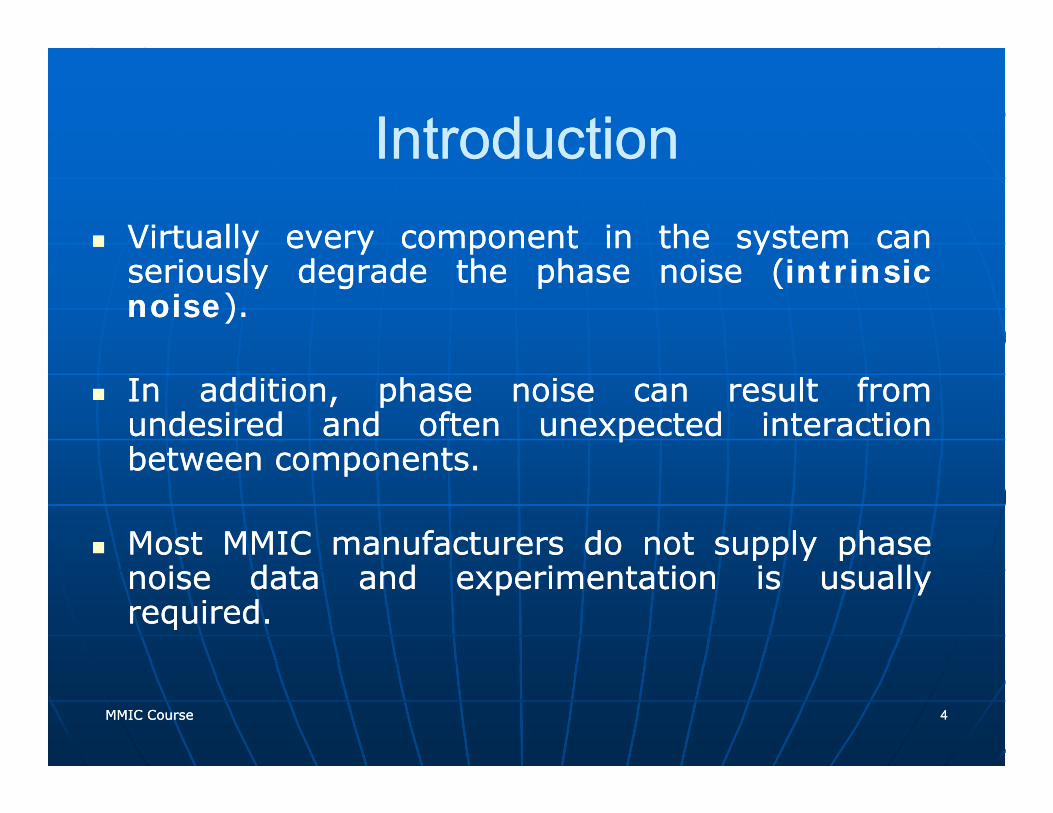
IntroductionIntroductionIntroductionIntroductionVirtually every component in the system can Virtually every component in the system can y y p yy y p yseriously degrade the phase noise (seriously degrade the phase noise (intrinsic intrinsic noisenoise).).
In addition, phase noise can result from In addition, phase noise can result from undesired and often unexpected interaction undesired and often unexpected interaction between componentsbetween componentsbetween components.between components.
Most MMIC manufacturers do not supply phase Most MMIC manufacturers do not supply phase pp y ppp y pnoise data and experimentation is usually noise data and experimentation is usually required.required.
MMIC CourseMMIC Course 44
OutlineOutlineOutlineOutline
IntroductionIntroductionIntroductionIntroductionPhase NoisePhase NoiseO t t Ph N i S tO t t Ph N i S tOutput Phase Noise SpectrumOutput Phase Noise SpectrumOn chip InductorsOn chip InductorsAdvanced On Chip InductorAdvanced On Chip Inductor
MMIC CourseMMIC Course 55
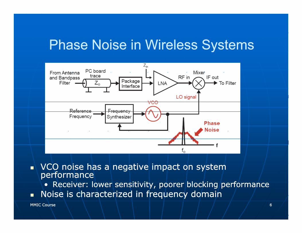
Phase Noise in Wireless SystemsPhase Noise in Wireless SystemsPhase Noise in Wireless Systems Phase Noise in Wireless Systems
VCO noise has a negative impact on system VCO noise has a negative impact on system performance performance •• Receiver: lower sensitivity, poorer blocking performance Receiver: lower sensitivity, poorer blocking performance
MMIC CourseMMIC Course 66
Noise is characterized in frequency domain Noise is characterized in frequency domain
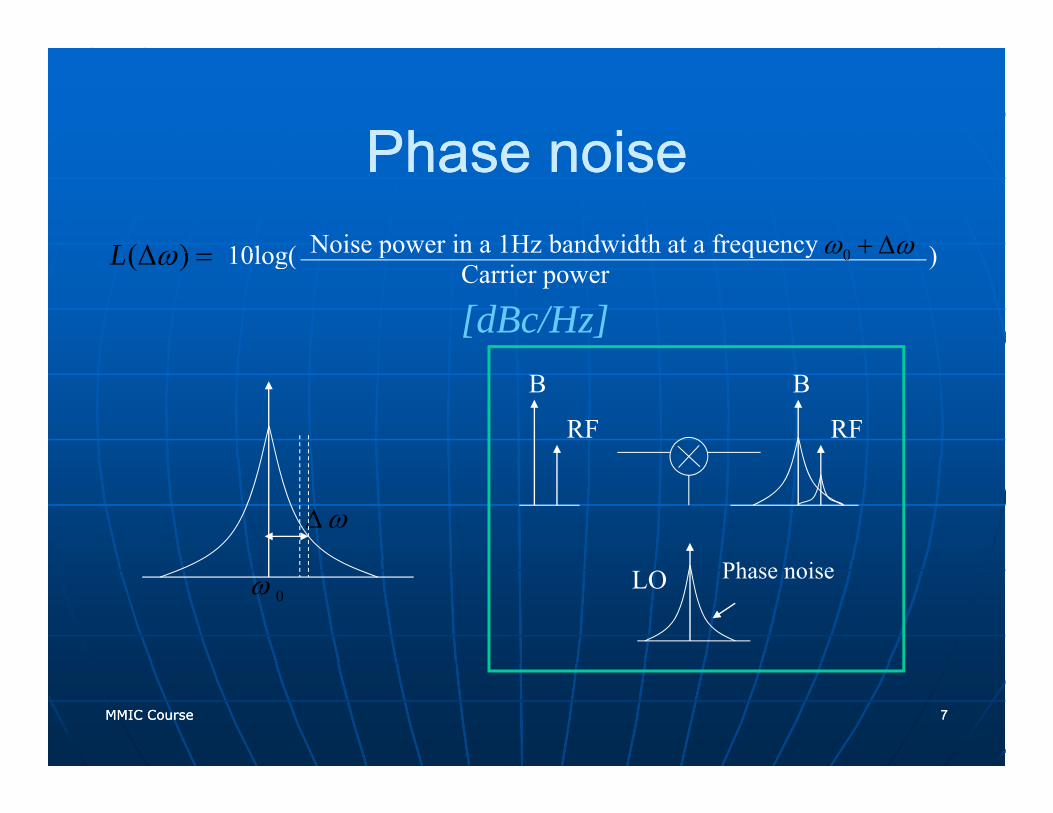
Phase noisePhase noisePhase noisePhase noiseΔ )( ωL 10log( Noise power in a 1Hz bandwidth at a frequency ωω Δ+0 )
[dBc/Hz]
=Δ )( ωL 10log( p q yCarrier power
ωω Δ+0 )
RF
B
RF
B
ωΔ
0ω Phase noiseLO
MMIC CourseMMIC Course 77
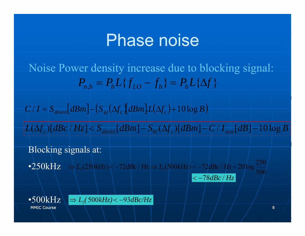
Phase noisePhase noisePhase noisePhase noiseNoise Power density increase due to blocking signal:
}{}{, fLPffLPP bbLObbn Δ=−=
( )
y g g
BdBICdBmfSdBmSHzdBcfL cbldésiréc log10][/])[(][]/)[( min −−Δ−<Δ
[ ] ( )[ ] ( )( )BfLdBmfSdBmSIC ccbldésiré log10./ +ΔΔ−=
ff cbldésiréc g)()( min
Blocking signals at:250•250kHz500250log20/72)500(/72)250( 11 +−=⇒−<⇒ HzdBckHzLHzdBckHzL
HzdBc /78−<
MMIC CourseMMIC Course 88•500kHz dBc/HzkHz)(L 935002 −<⇒
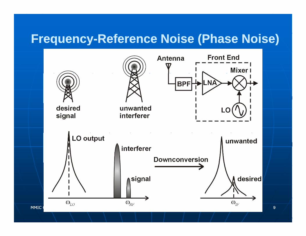
FrequencyFrequency--Reference Noise (Phase Noise)Reference Noise (Phase Noise)q yq y ( )( )
MMIC CourseMMIC Course 99
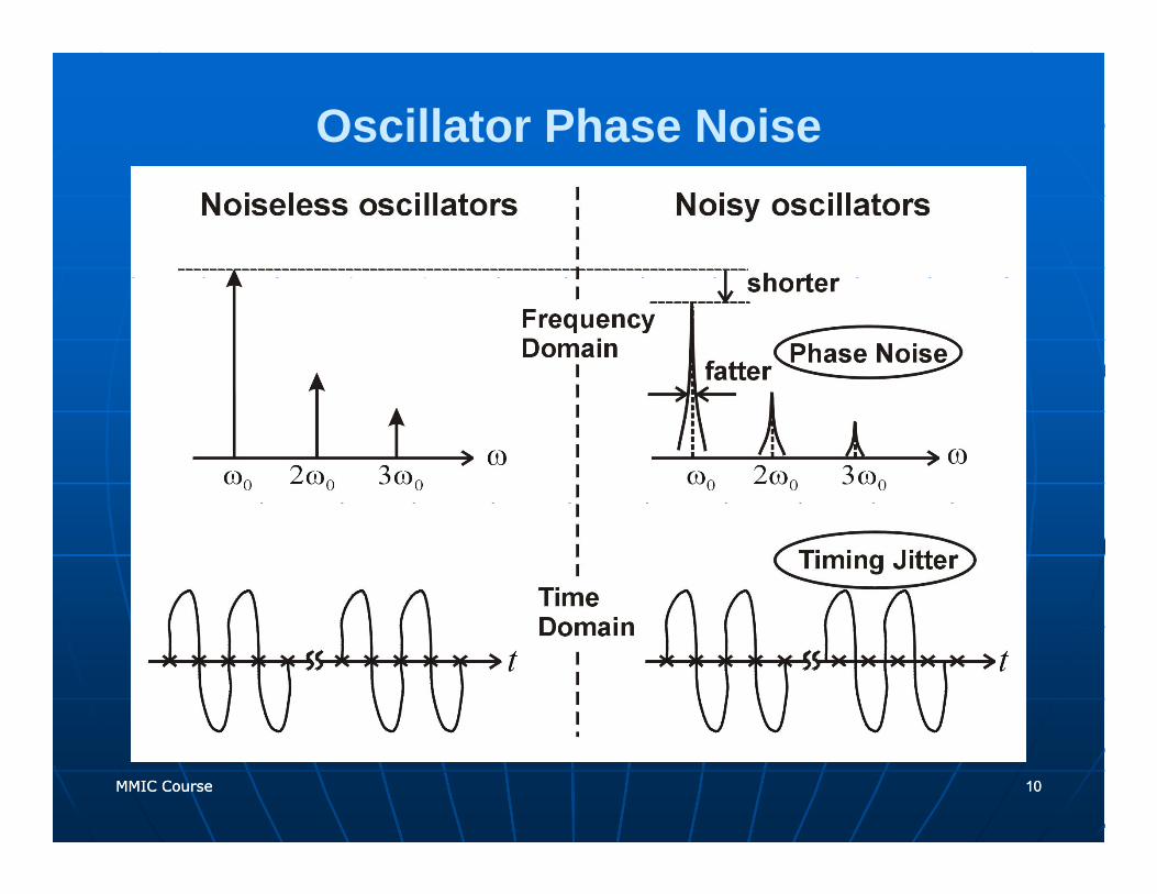
Oscillator Phase Noise
MMIC CourseMMIC Course 1010
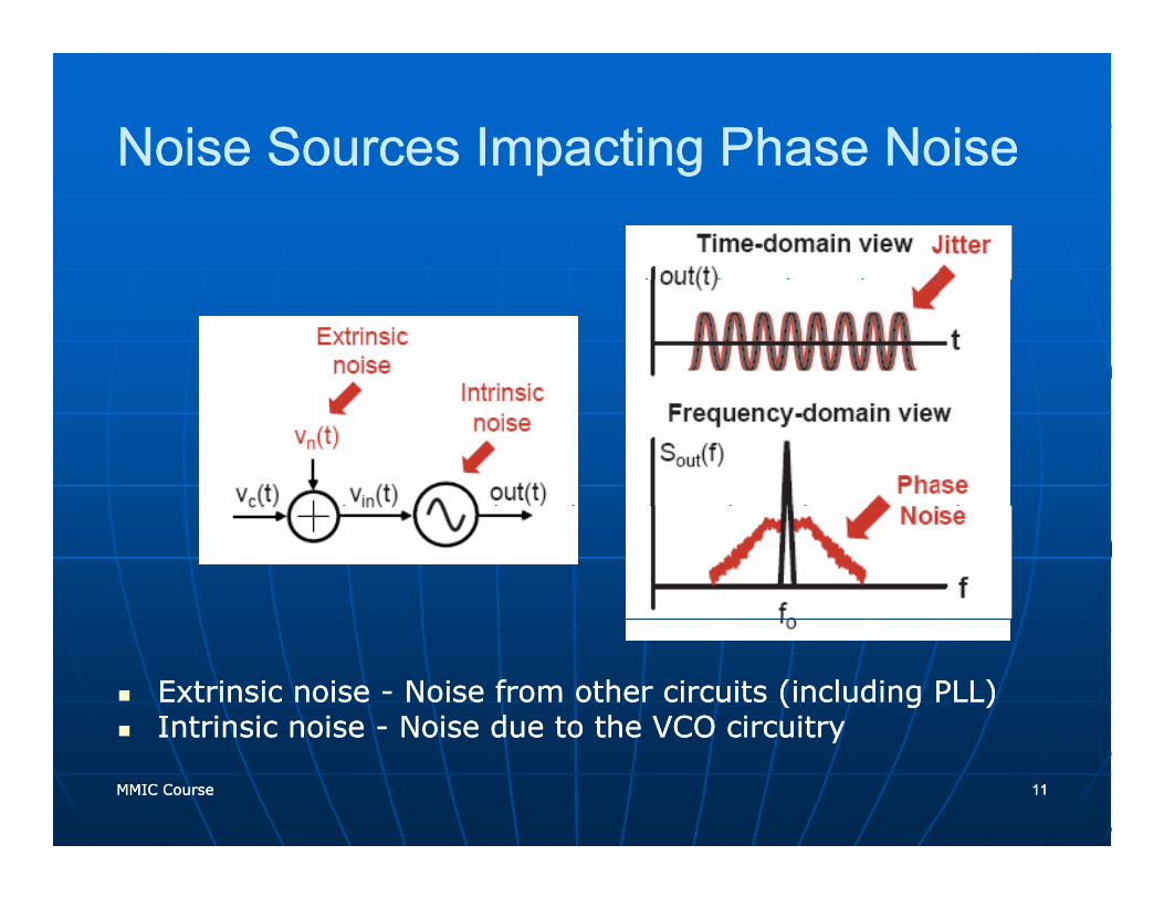
Noise Sources Impacting Phase Noise Noise Sources Impacting Phase Noise p gp g
Extrinsic noise Extrinsic noise -- Noise from other circuits (including PLL) Noise from other circuits (including PLL) Intrinsic noise Intrinsic noise -- Noise due to the VCO circuitry Noise due to the VCO circuitry
MMIC CourseMMIC Course 1111
Intrinsic noise Intrinsic noise Noise due to the VCO circuitry Noise due to the VCO circuitry
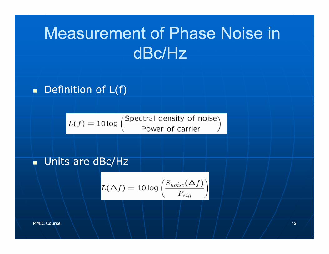
Measurement of Phase Noise in Measurement of Phase Noise in dB /HdB /HdBc/Hz dBc/Hz
Definition of L(f)Definition of L(f)
Units are dBc/HzUnits are dBc/Hz
MMIC CourseMMIC Course 1212
OutlineOutlineOutlineOutline
IntroductionIntroductionIntroductionIntroductionPhase NoisePhase NoiseO t t Ph N i S tO t t Ph N i S tOutput Phase Noise SpectrumOutput Phase Noise SpectrumOn chip InductorsOn chip InductorsAdvanced On Chip InductorAdvanced On Chip Inductor
MMIC CourseMMIC Course 1313
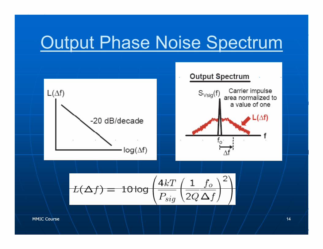
Output Phase Noise SpectrumOutput Phase Noise Spectrum
MMIC CourseMMIC Course 1414
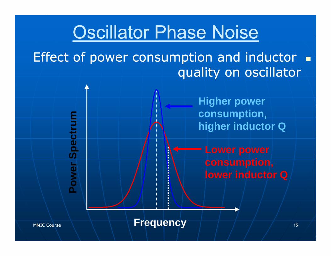
Oscillator Phase NoiseOscillator Phase NoiseEffect of power consumption and inductor Effect of power consumption and inductor
quality on oscillatorquality on oscillator
Higher power consumptionm consumption, higher inductor Q
ectr
um
Lower power consumption, lower inductor Qw
er S
pe
lower inductor Q
Pow
MMIC CourseMMIC Course 1515Frequency
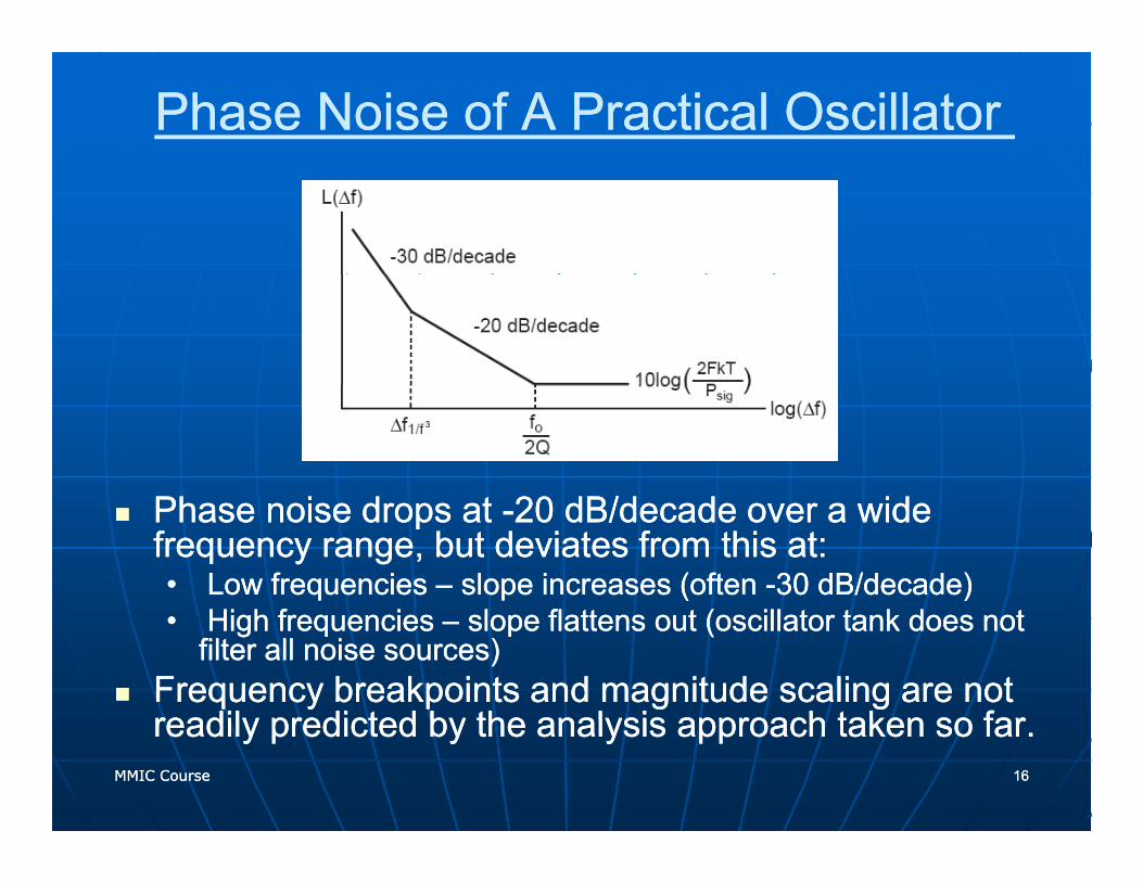
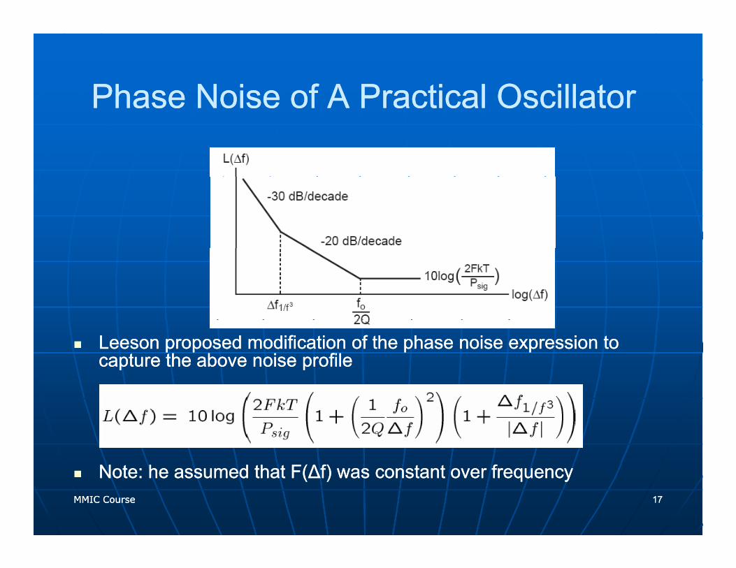
Phase Noise of A Practical Oscillator Phase Noise of A Practical Oscillator
Ph i dPh i d 2020 dB/d d iddB/d d idPhase noise drops at Phase noise drops at --20 20 dB/decade over a wide dB/decade over a wide frequency range, but deviates from this at:frequency range, but deviates from this at:•• Low frequencies Low frequencies –– slope increases (often slope increases (often --30 30 dB/decade)dB/decade)•• High frequencies High frequencies –– slope flattens out (oscillator tank does not slope flattens out (oscillator tank does not
filter all noise sources) filter all noise sources) Frequency breakpoints and magnitude scaling are not Frequency breakpoints and magnitude scaling are not readily predicted by the analysis approach taken so farreadily predicted by the analysis approach taken so far
MMIC CourseMMIC Course 1616
readily predicted by the analysis approach taken so far. readily predicted by the analysis approach taken so far.
Phase Noise of A Practical OscillatorPhase Noise of A Practical OscillatorPhase Noise of A Practical Oscillator Phase Noise of A Practical Oscillator
Leeson proposed modification of the phase noise expression to Leeson proposed modification of the phase noise expression to capture the above noise profilecapture the above noise profile
MMIC CourseMMIC Course 1717
Note: he assumed that F(∆f) was constant over frequency Note: he assumed that F(∆f) was constant over frequency
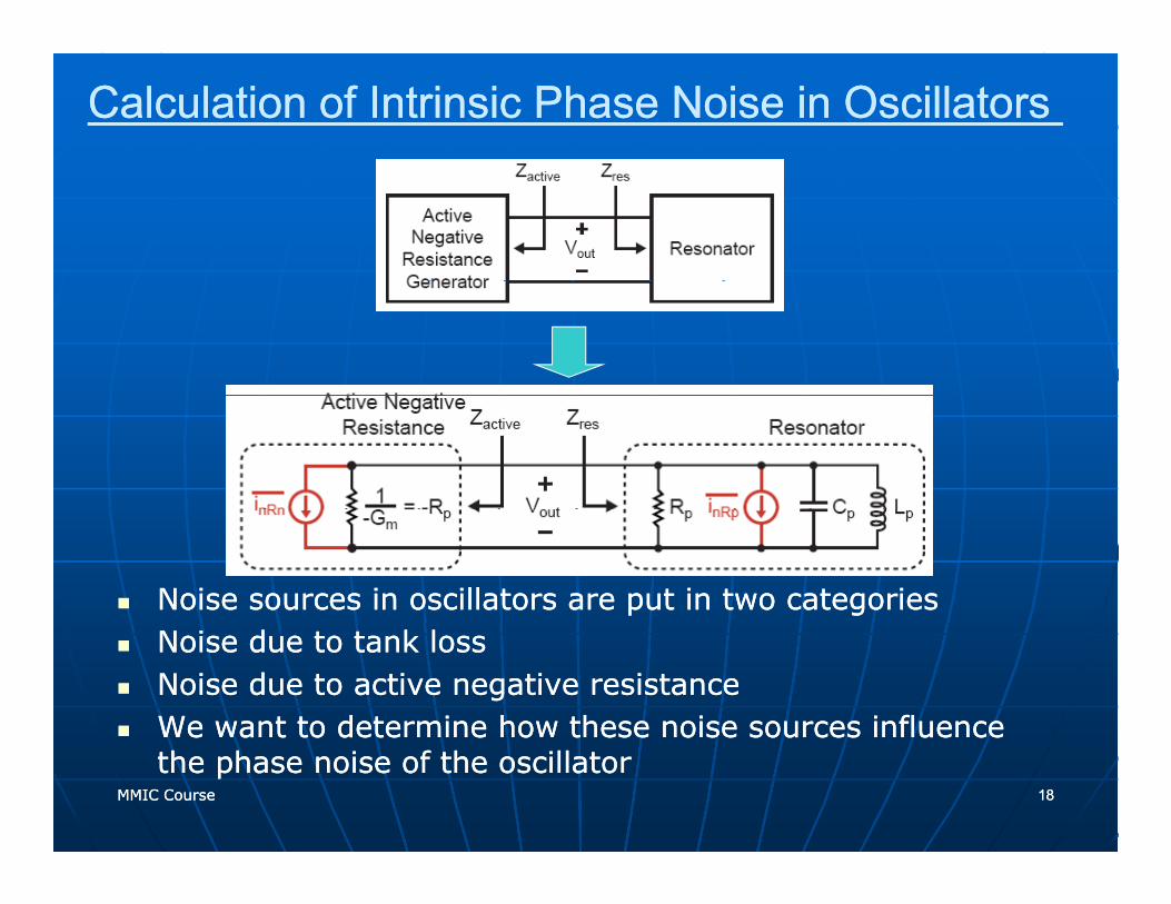
Calculation of Intrinsic Phase Noise in Oscillators Calculation of Intrinsic Phase Noise in Oscillators
Noise sources in oscillators are put in two categories Noise sources in oscillators are put in two categories Noise due to tank loss Noise due to tank loss Noise due to active negative resistance Noise due to active negative resistance We want to determine how these noise sources influence We want to determine how these noise sources influence
MMIC CourseMMIC Course 1818
e a t to dete e o t ese o se sou ces ue cee a t to dete e o t ese o se sou ces ue cethe phase noise of the oscillator the phase noise of the oscillator
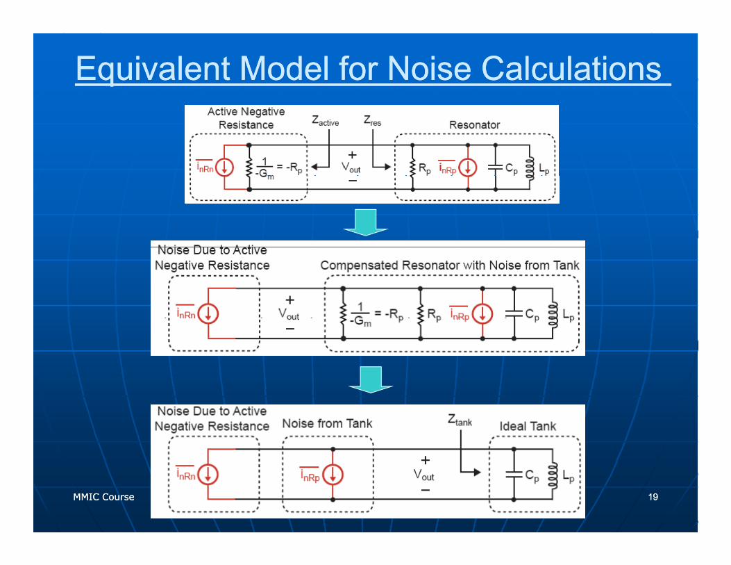
Equivalent Model for Noise Calculations Equivalent Model for Noise Calculations
MMIC CourseMMIC Course 1919
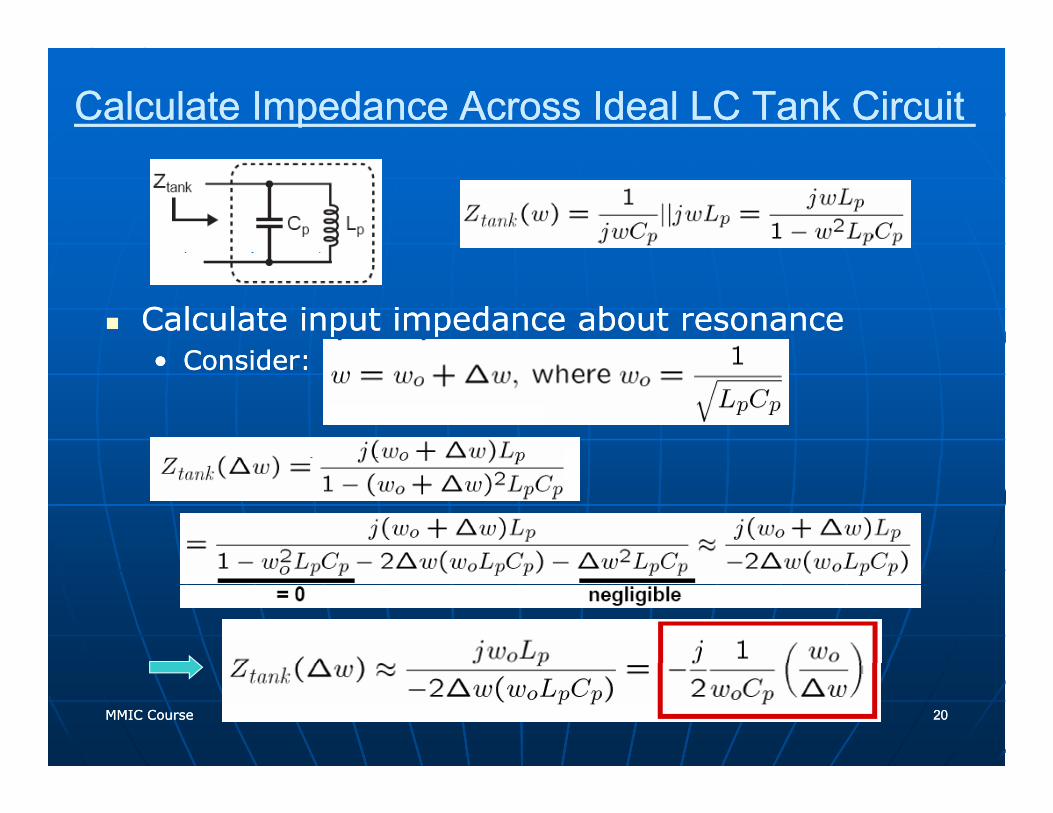
Calculate Impedance Across Ideal LC Tank Circuit Calculate Impedance Across Ideal LC Tank Circuit
Calculate input impedance about resonance Calculate input impedance about resonance Consider: Consider: •• Consider: Consider:
MMIC CourseMMIC Course 2020
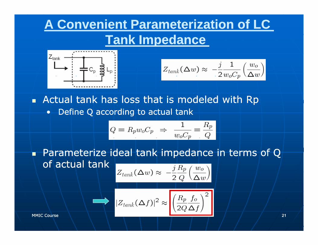
A Convenient Parameterization of LC A Convenient Parameterization of LC Tank ImpedanceTank Impedancepp
Actual tank has loss that is modeled with Rp Actual tank has loss that is modeled with Rp •• Define Q according to actual tank Define Q according to actual tank
Parameterize ideal tank impedance in terms of Q Parameterize ideal tank impedance in terms of Q of actual tank of actual tank
MMIC CourseMMIC Course 2121
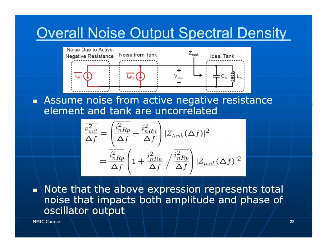
Overall Noise Output Spectral Density Overall Noise Output Spectral Density
Assume noise from active negative resistance Assume noise from active negative resistance element and tank are uncorrelatedelement and tank are uncorrelatedelement and tank are uncorrelatedelement and tank are uncorrelated
Note that the above expression represents total Note that the above expression represents total noise that impacts both amplitude and phase of noise that impacts both amplitude and phase of
MMIC CourseMMIC Course 2222
oscillator output oscillator output
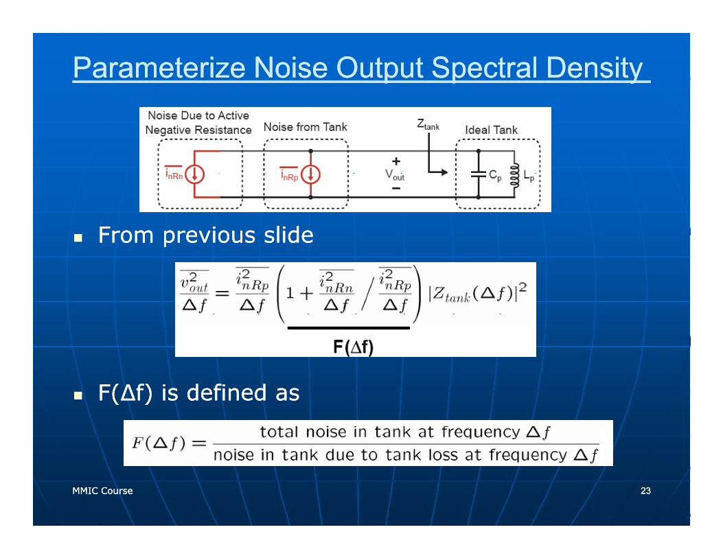
Parameterize Noise Output Spectral Density Parameterize Noise Output Spectral Density
From previous slide From previous slide pp
F(Δf) i d fi d F(Δf) i d fi d F(Δf) is defined as F(Δf) is defined as
MMIC CourseMMIC Course 2323
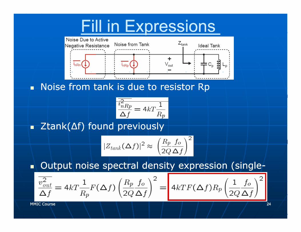
Fill in Expressions Fill in Expressions
Noise from tank is due to resistor Rp Noise from tank is due to resistor Rp
Ztank(Δf) found previously Ztank(Δf) found previously ( ) p y( ) p y
Output noise spectral density expression (singleOutput noise spectral density expression (single--sided) sided)
MMIC CourseMMIC Course 2424
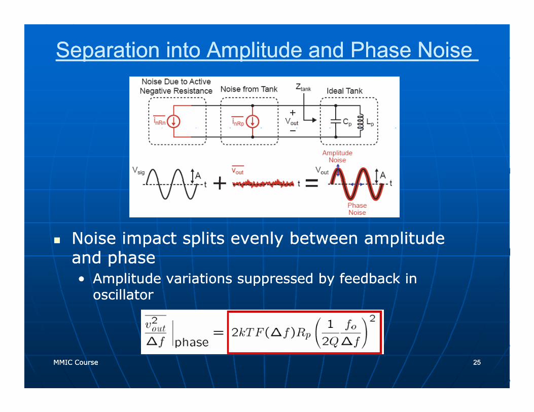
Separation into Amplitude and Phase Noise Separation into Amplitude and Phase Noise
N i i li l b li d N i i li l b li d Noise impact splits evenly between amplitude Noise impact splits evenly between amplitude and phaseand phase•• Amplitude variations suppressed by feedback in Amplitude variations suppressed by feedback in p pp yp pp y
oscillator oscillator
MMIC CourseMMIC Course 2525
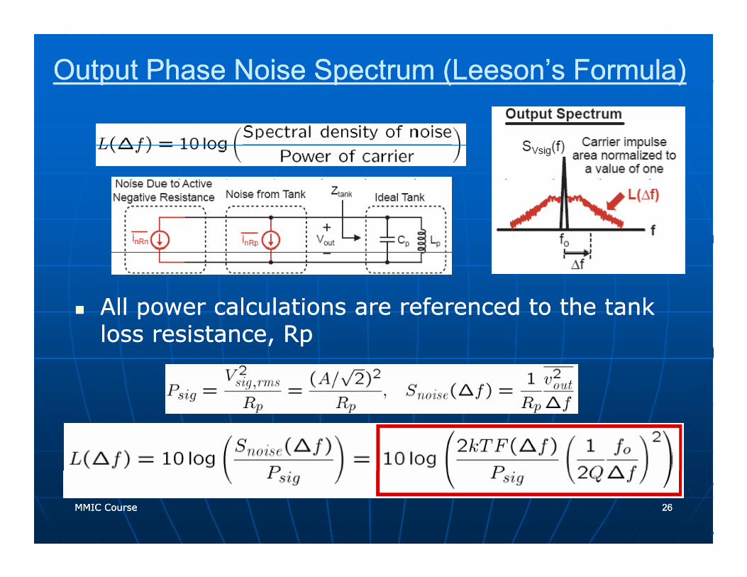
Output Phase Noise Spectrum (Leeson’s Formula)Output Phase Noise Spectrum (Leeson’s Formula)
All power calculations are referenced to the tank All power calculations are referenced to the tank llloss resistance, Rp loss resistance, Rp
MMIC CourseMMIC Course 2626
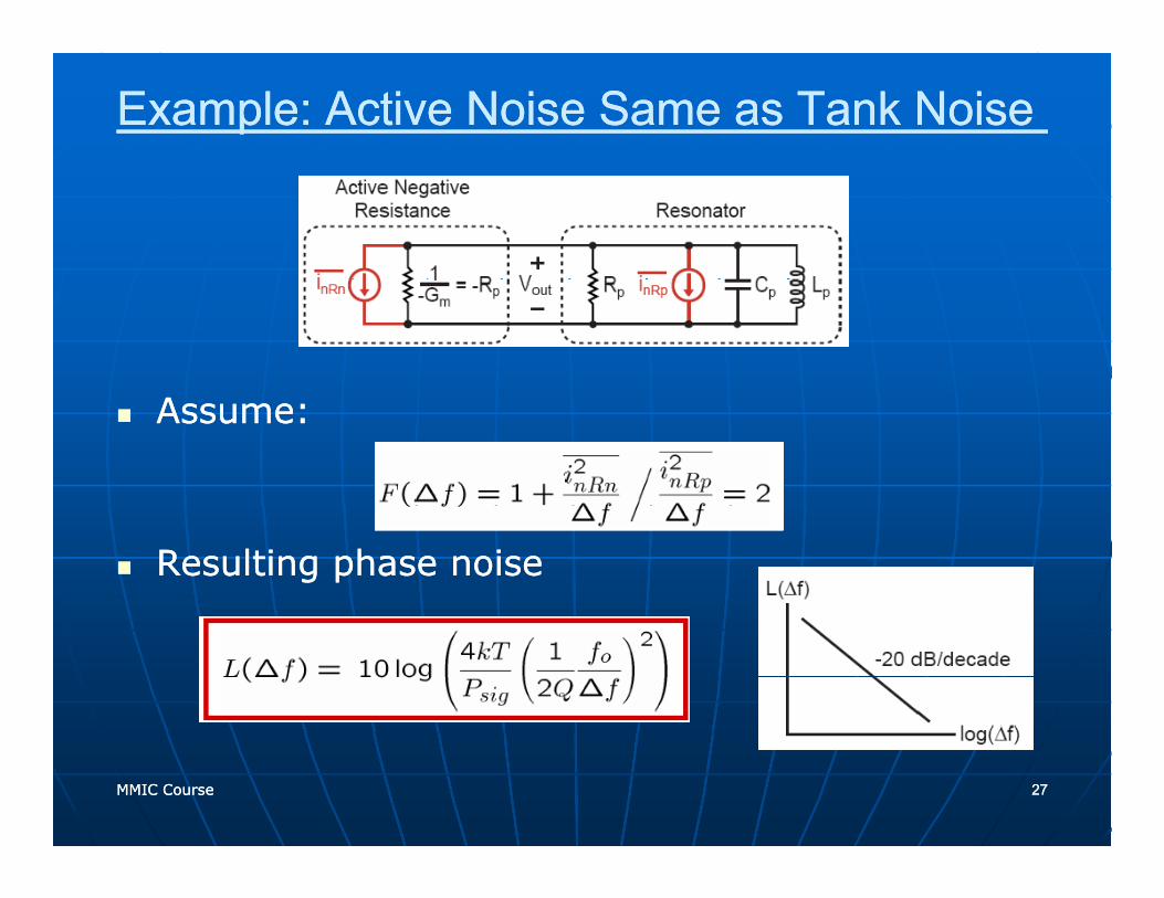
Example: Active Noise Same as Tank Noise Example: Active Noise Same as Tank Noise
Assume:Assume:
Resulting phase noise Resulting phase noise
MMIC CourseMMIC Course 2727
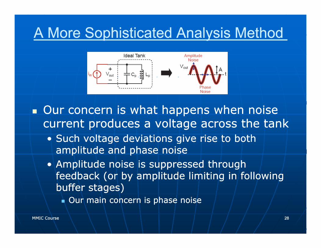
A More Sophisticated Analysis Method A More Sophisticated Analysis Method
Our concern is what happens when noise Our concern is what happens when noise Our concern is what happens when noise Our concern is what happens when noise current produces a voltage across the tank current produces a voltage across the tank •• Such voltage deviations give rise to both Such voltage deviations give rise to both •• Such voltage deviations give rise to both Such voltage deviations give rise to both
amplitude and phase noise amplitude and phase noise •• Amplitude noise is suppressed through Amplitude noise is suppressed through
feedback (or by amplitude limiting in following feedback (or by amplitude limiting in following buffer stages) buffer stages)
Our main concern is phase noise Our main concern is phase noise
MMIC CourseMMIC Course 2828
Our main concern is phase noise Our main concern is phase noise
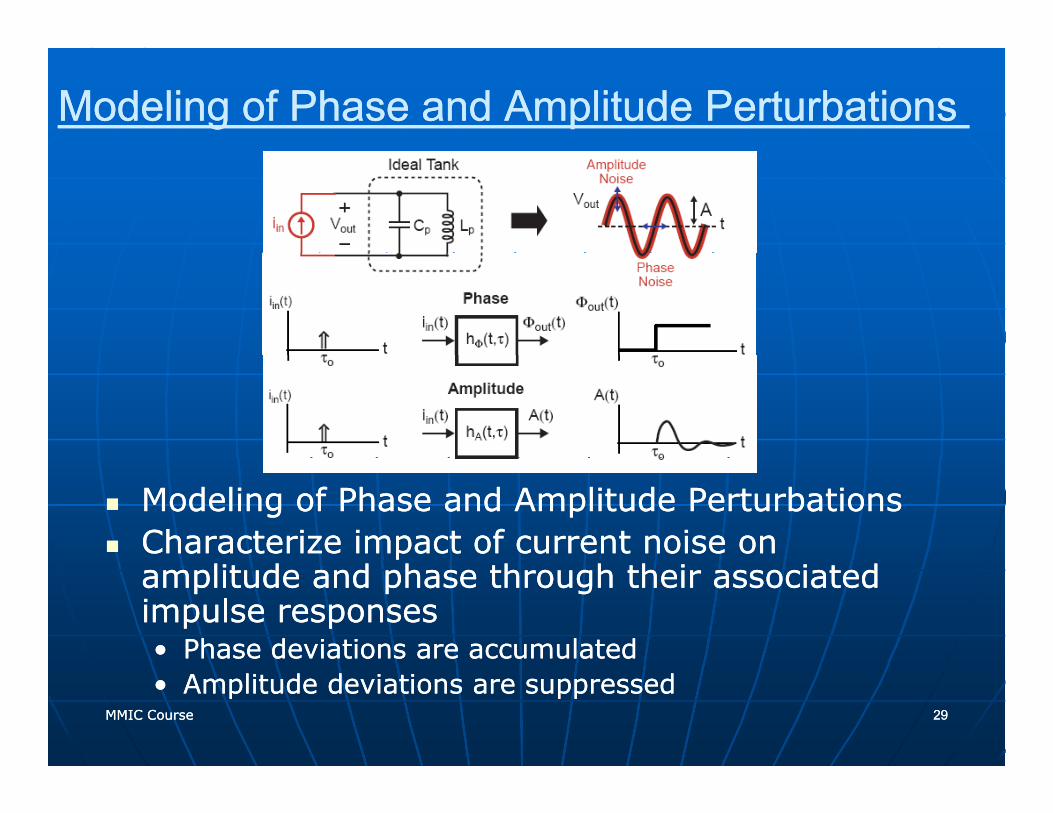
Modeling of Phase and Amplitude Perturbations Modeling of Phase and Amplitude Perturbations
Modeling of Phase and Amplitude Perturbations Modeling of Phase and Amplitude Perturbations Characterize impact of current noise on Characterize impact of current noise on amplitude and phase through their associated amplitude and phase through their associated impulse responsesimpulse responses•• Phase deviations are accumulated Phase deviations are accumulated
MMIC CourseMMIC Course 2929
•• Amplitude deviations are suppressed Amplitude deviations are suppressed
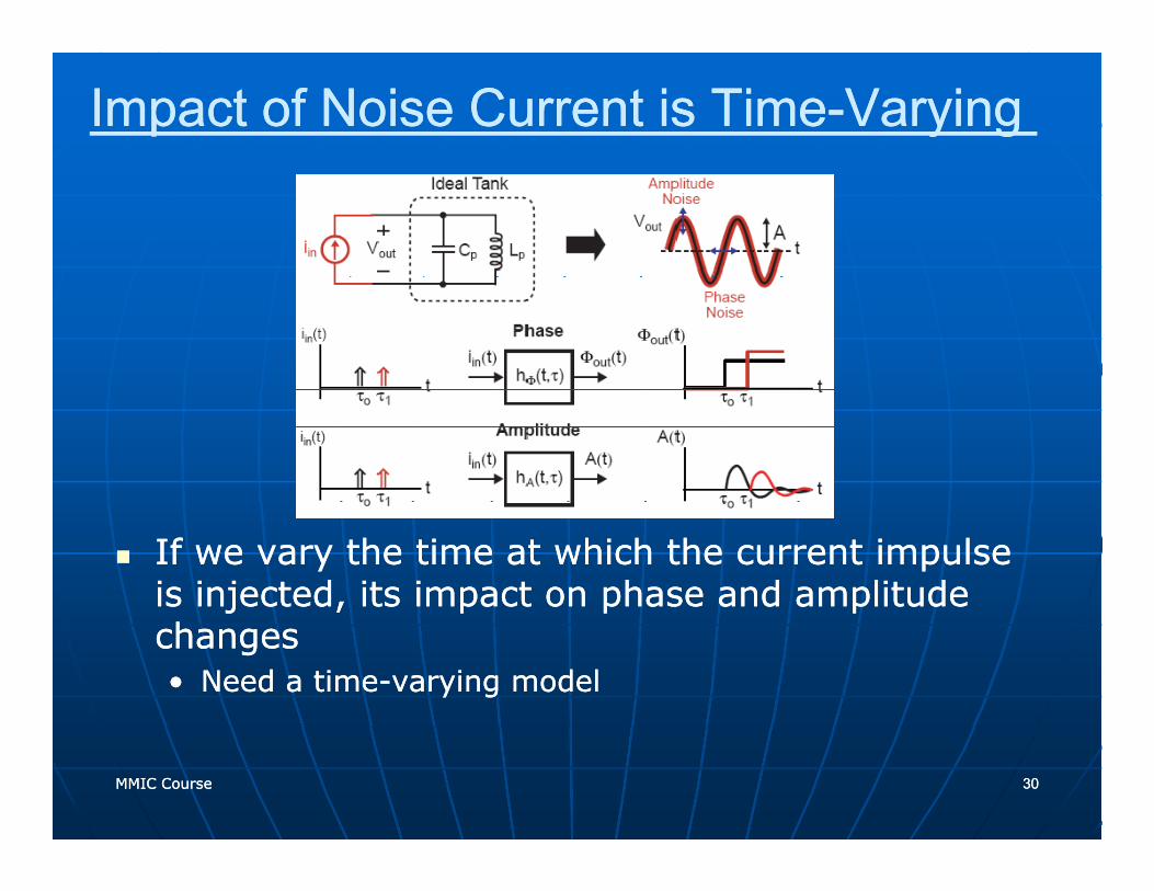
Varying Varying --Impact of Noise Current is TimeImpact of Noise Current is Time
If we vary the time at which the current impulse If we vary the time at which the current impulse is injected, its impact on phase and amplitude is injected, its impact on phase and amplitude changeschanges•• Need a timeNeed a time--varying model varying model
MMIC CourseMMIC Course 3030
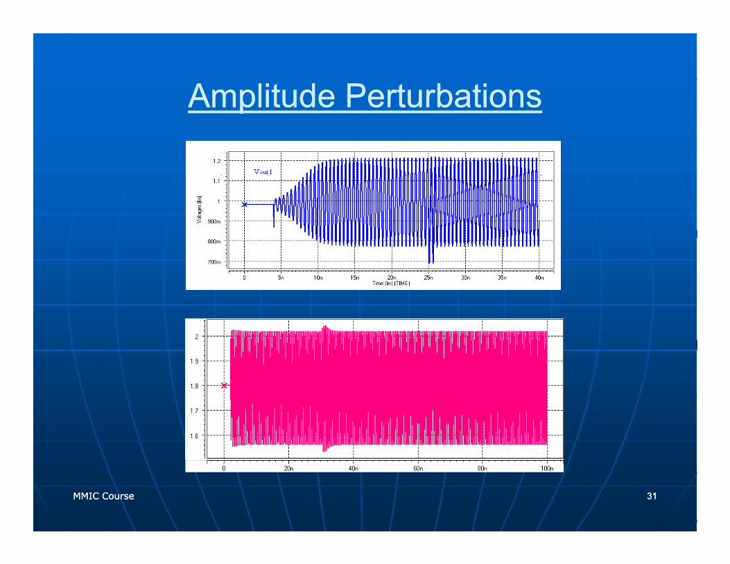
Amplitude PerturbationsAmplitude PerturbationsAmplitude PerturbationsAmplitude Perturbations
MMIC CourseMMIC Course 3131
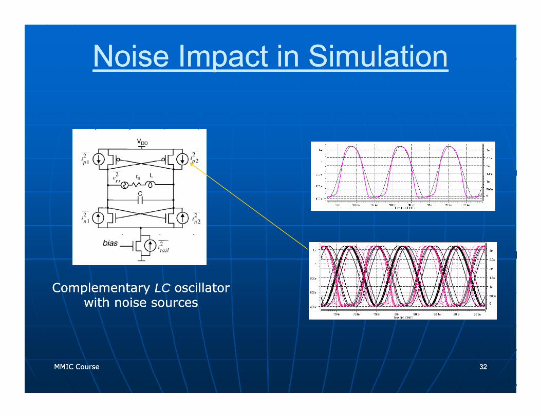
Noise Impact in SimulationNoise Impact in Simulation
Complementary Complementary LC LC oscillator oscillator Complementary Complementary LC LC oscillator oscillator with noise sourceswith noise sources
MMIC CourseMMIC Course 3232
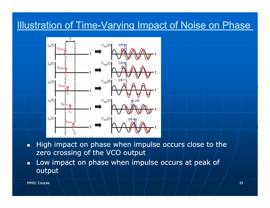
Varying Impact of Noise on Phase Varying Impact of Noise on Phase --Illustration of TimeIllustration of Time
High impact on phase when impulse occurs close to the High impact on phase when impulse occurs close to the High impact on phase when impulse occurs close to the High impact on phase when impulse occurs close to the zero crossing of the VCO output zero crossing of the VCO output Low impact on phase when impulse occurs at peak of Low impact on phase when impulse occurs at peak of output output
MMIC CourseMMIC Course 3333
output output
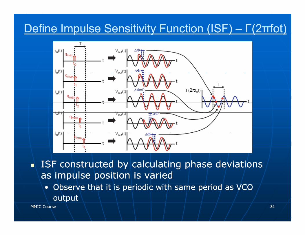
Define Impulse Sensitivity Function (ISF) Define Impulse Sensitivity Function (ISF) –– Γ(Γ(22πfot)πfot)
ISF t t d b l l ti h d i ti ISF t t d b l l ti h d i ti ISF constructed by calculating phase deviations ISF constructed by calculating phase deviations as impulse position is variedas impulse position is varied•• Observe that it is periodic with same period as VCO Observe that it is periodic with same period as VCO
MMIC CourseMMIC Course 3434
outputoutput
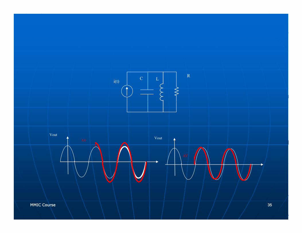
i(t) C LR
∆V
∆VVout
Vout
MMIC CourseMMIC Course 3535
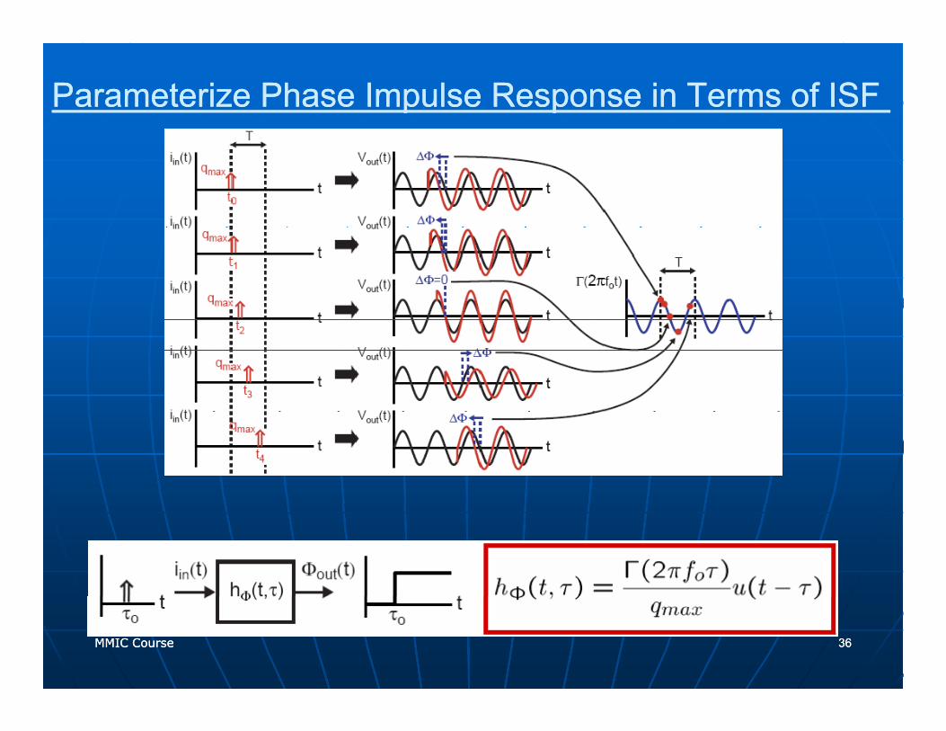
Parameterize Phase Impulse Response in Terms of ISFParameterize Phase Impulse Response in Terms of ISF
MMIC CourseMMIC Course 3636
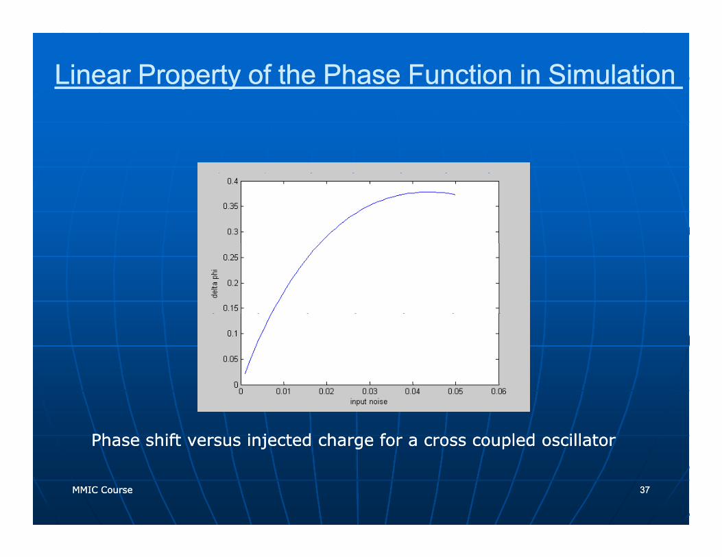
Linear Property of the Phase Function in Simulation Linear Property of the Phase Function in Simulation
Phase shift versus injected charge for a cross coupled oscillatorPhase shift versus injected charge for a cross coupled oscillator
MMIC CourseMMIC Course 3737
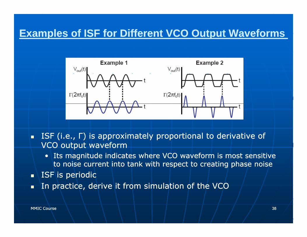
Examples of ISF for Different VCO Output WaveformsExamples of ISF for Different VCO Output Waveforms
ISF (i Γ) i i t l ti l t d i ti f ISF (i Γ) i i t l ti l t d i ti f ISF (i.e., Γ) is approximately proportional to derivative of ISF (i.e., Γ) is approximately proportional to derivative of VCO output waveformVCO output waveform•• Its magnitude indicates where VCO waveform is most sensitive Its magnitude indicates where VCO waveform is most sensitive
to noise current into tank with respect to creating phase noiseto noise current into tank with respect to creating phase noiseto noise current into tank with respect to creating phase noiseto noise current into tank with respect to creating phase noiseISF is periodicISF is periodicIn practice, derive it from simulation of the VCO In practice, derive it from simulation of the VCO
MMIC CourseMMIC Course 3838
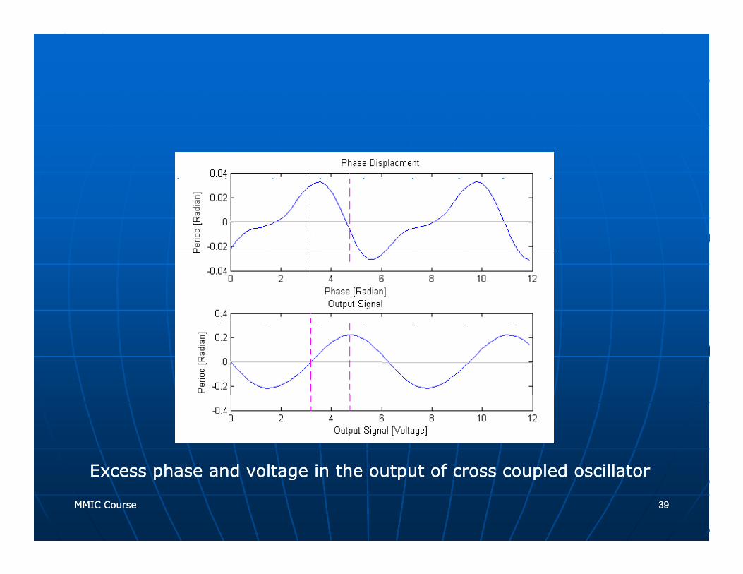
Excess phase and voltage in the output of cross coupled oscillator Excess phase and voltage in the output of cross coupled oscillator
MMIC CourseMMIC Course 3939
Excess phase and voltage in the output of cross coupled oscillator Excess phase and voltage in the output of cross coupled oscillator
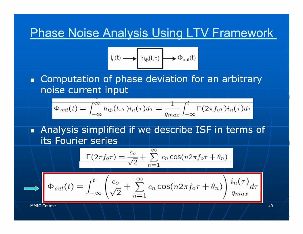
Phase Noise Analysis Using LTV Framework Phase Noise Analysis Using LTV Framework
Computation of phase deviation for an arbitrary Computation of phase deviation for an arbitrary noise current input noise current input
Analysis simplified if we describe ISF in terms of Analysis simplified if we describe ISF in terms of Analysis simplified if we describe ISF in terms of Analysis simplified if we describe ISF in terms of its Fourier seriesits Fourier series
MMIC CourseMMIC Course 4040
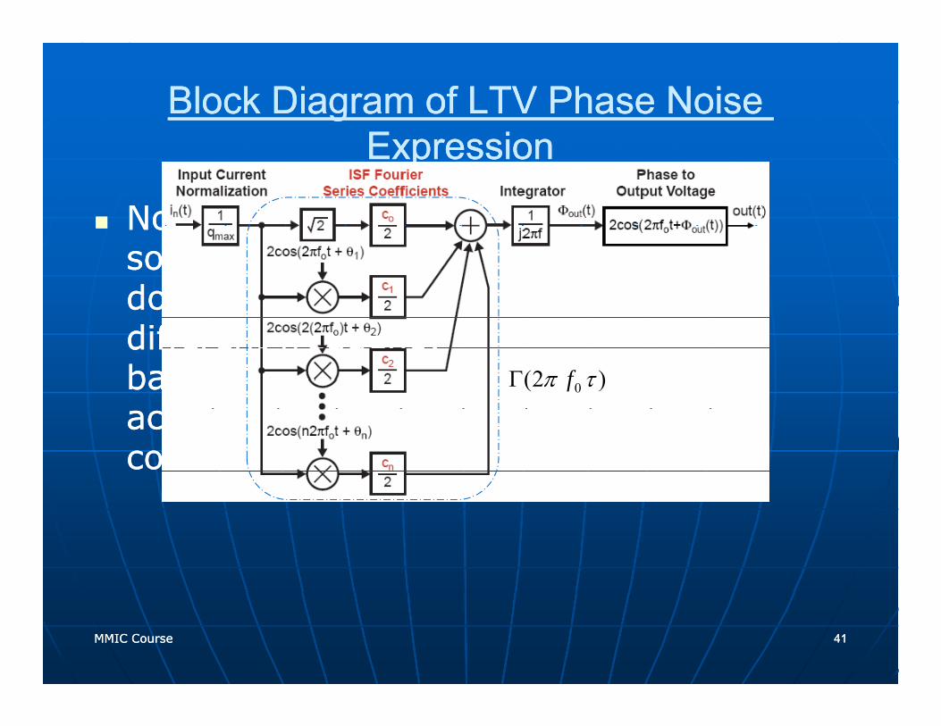
Block Diagram of LTV Phase Noise Block Diagram of LTV Phase Noise E iE iExpression Expression
Noise from current Noise from current Noise from current Noise from current source is mixed source is mixed down from down from different frequency different frequency bands and scaled bands and scaled
di t ISF di t ISF )2( 0τπ fΓ
according to ISF according to ISF coefficients coefficients
MMIC CourseMMIC Course 4141
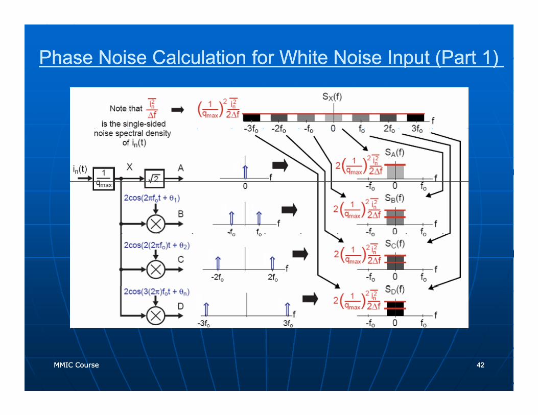
) ) 11Phase Noise Calculation for White Noise Input (Part Phase Noise Calculation for White Noise Input (Part
MMIC CourseMMIC Course 4242
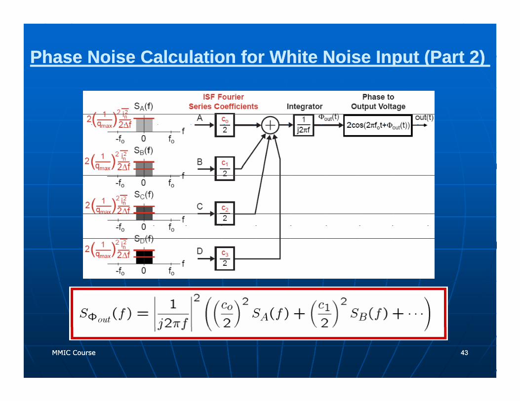
))22Phase Noise Calculation for White Noise Input (Part Phase Noise Calculation for White Noise Input (Part
MMIC CourseMMIC Course 4343
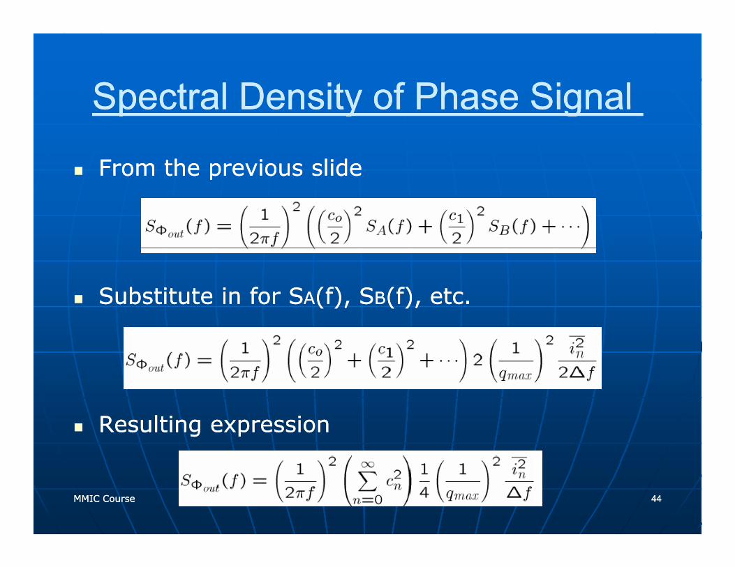
Spectral Density of Phase SignalSpectral Density of Phase SignalSpectral Density of Phase Signal Spectral Density of Phase Signal
From the previous slide From the previous slide pp
Substitute in for SSubstitute in for SAA(f), S(f), SBB(f), etc. (f), etc.
Resulting expressionResulting expression
MMIC CourseMMIC Course 4444
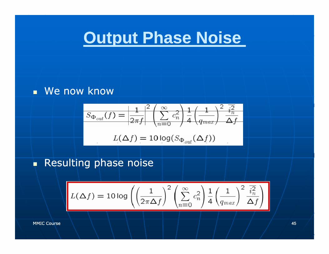
Output Phase NoiseOutput Phase Noise
We now know We now know
Resulting phase noise Resulting phase noise
MMIC CourseMMIC Course 4545
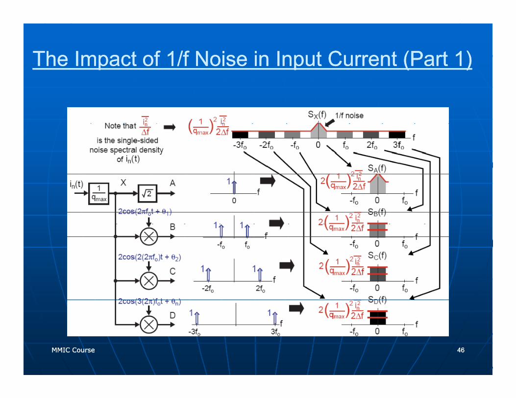
))11/f Noise in Input Current (Part /f Noise in Input Current (Part 11The Impact of The Impact of
MMIC CourseMMIC Course 4646
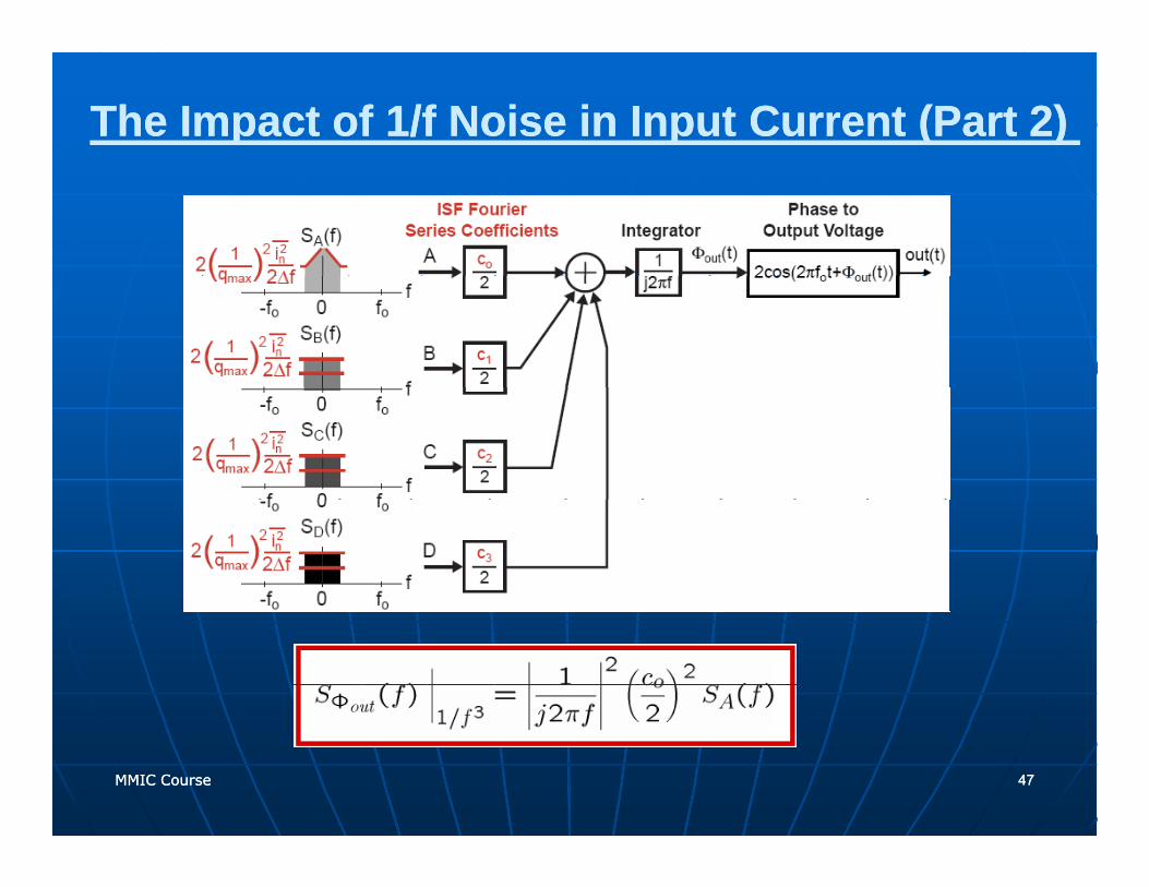
))22/f Noise in Input Current (Part /f Noise in Input Current (Part 11The Impact of The Impact of
MMIC CourseMMIC Course 4747
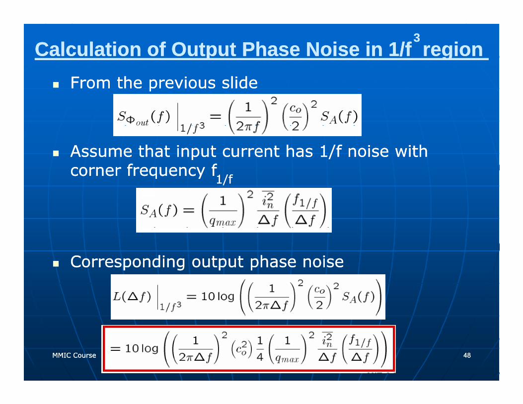
/f region/f region11Calculation of Output Phase Noise in Calculation of Output Phase Noise in 33
From the previous slide From the previous slide
Assume that input current has Assume that input current has 11/f noise with /f noise with corner frequency fcorner frequency f11/f/fq yq y 11/f/f
Corresponding output phase noiseCorresponding output phase noise
MMIC CourseMMIC Course 4848
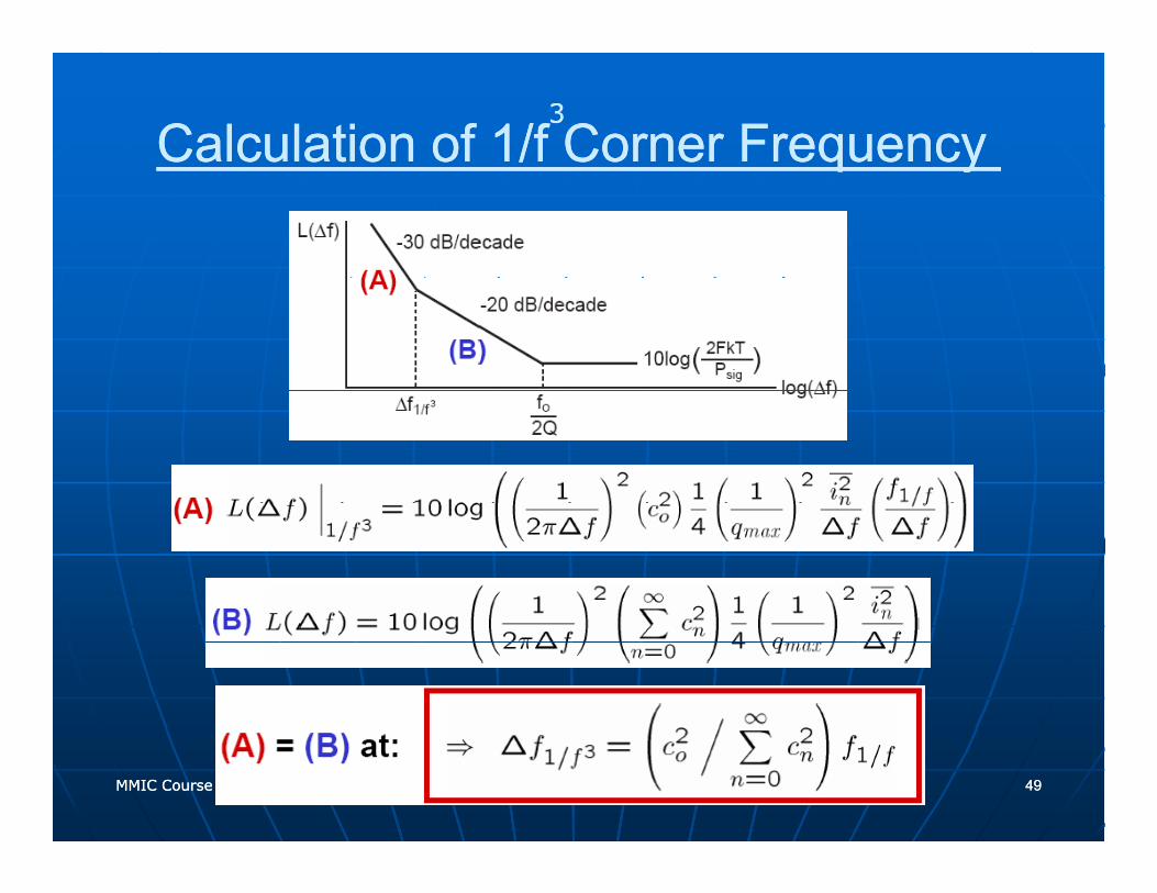
/f Corner Frequency /f Corner Frequency 11Calculation of Calculation of 33
q yq y
MMIC CourseMMIC Course 4949
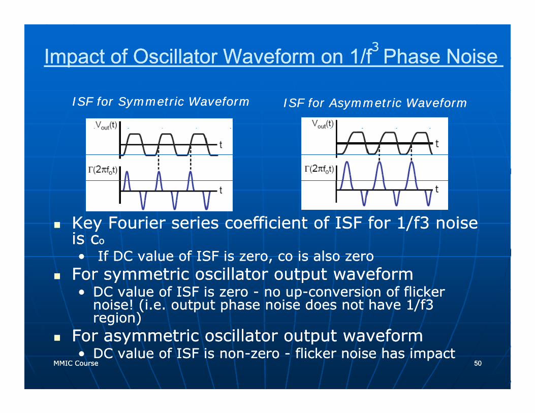
/f Phase Noise /f Phase Noise 11Impact of Oscillator Waveform on Impact of Oscillator Waveform on 33
ISF for Symmetric Waveform ISF for Symmetric Waveform ISF for Asymmetric Waveform ISF for Asymmetric Waveform
Key Fourier series coefficient of ISF for Key Fourier series coefficient of ISF for 11/f/f3 3 noise noise i i is cis coo
•• If DC value of ISF is zero, co is also zero If DC value of ISF is zero, co is also zero For symmetric oscillator output waveformFor symmetric oscillator output waveform•• DC value of ISF is zero DC value of ISF is zero -- no upno up--conversion of flicker conversion of flicker
noise! (i.e. output phase noise does not have noise! (i.e. output phase noise does not have 11/f/f3 3 region) region)
For asymmetric oscillator output waveformFor asymmetric oscillator output waveformMMIC CourseMMIC Course 5050
For asymmetric oscillator output waveformFor asymmetric oscillator output waveform•• DC value of ISF is nonDC value of ISF is non--zero zero -- flicker noise has impact flicker noise has impact
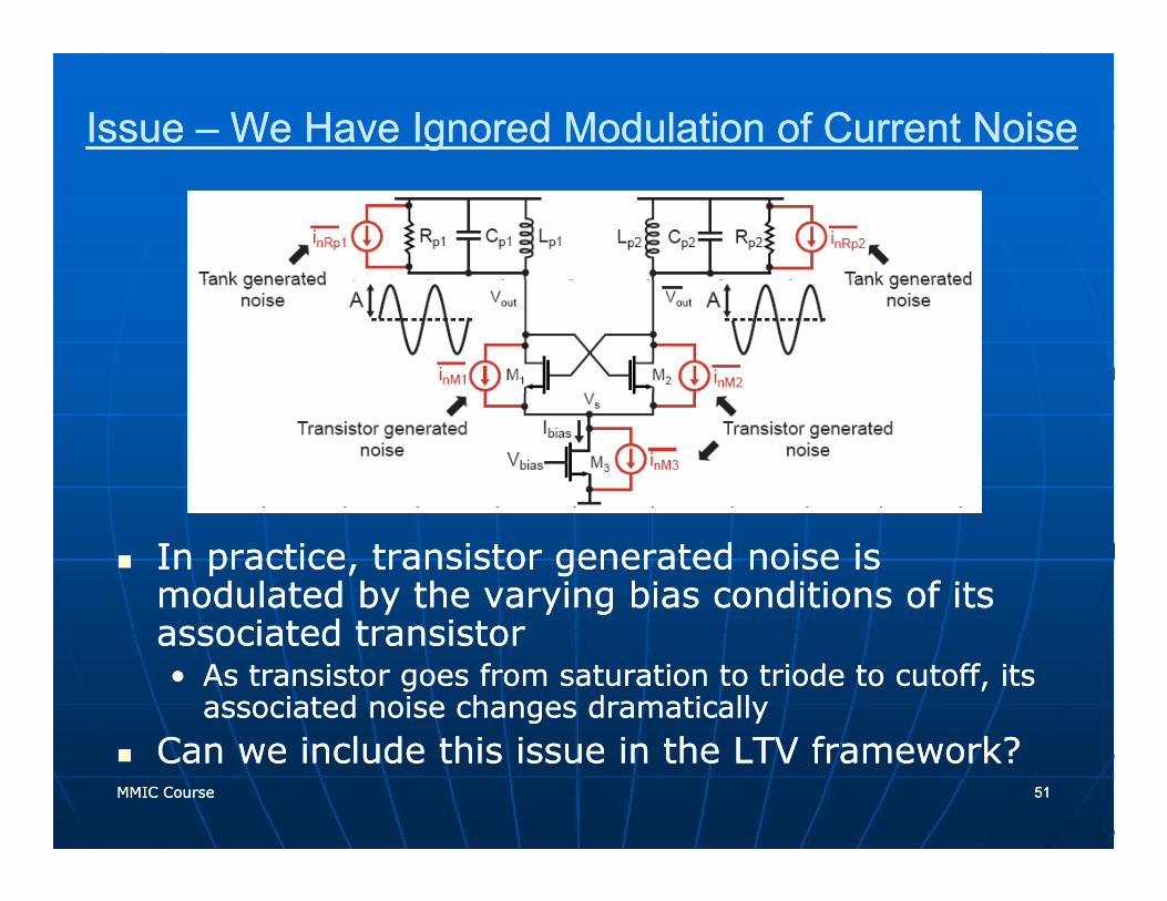
Issue Issue –– We Have Ignored Modulation of Current Noise We Have Ignored Modulation of Current Noise
In practice, transistor generated noise is In practice, transistor generated noise is modulated by the varying bias conditions of its modulated by the varying bias conditions of its
i t d t i ti t d t i tassociated transistorassociated transistor•• As transistor goes from saturation to triode to cutoff, its As transistor goes from saturation to triode to cutoff, its
associated noise changes dramaticallyassociated noise changes dramatically
MMIC CourseMMIC Course 5151
Can we include this issue in the LTV framework? Can we include this issue in the LTV framework?
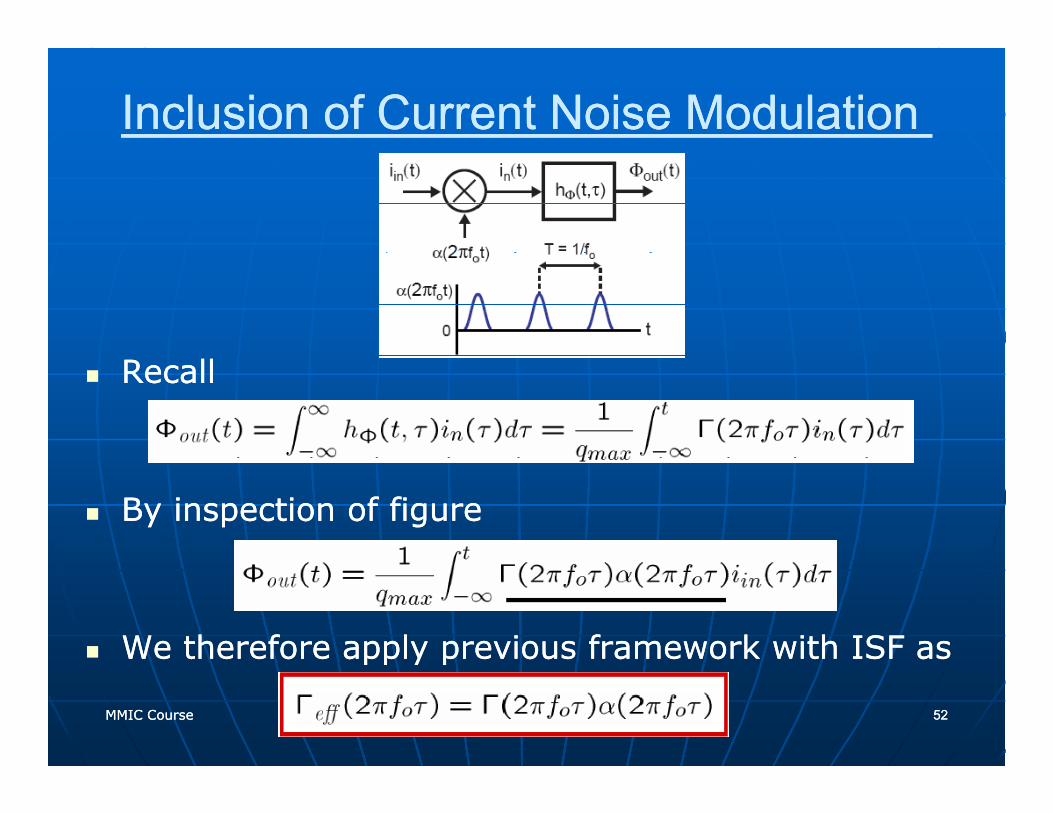
Inclusion of Current Noise Modulation Inclusion of Current Noise Modulation
Recall Recall
By inspection of figure By inspection of figure
We therefore apply previous framework with ISF as We therefore apply previous framework with ISF as
MMIC CourseMMIC Course 5252
pp y ppp y p
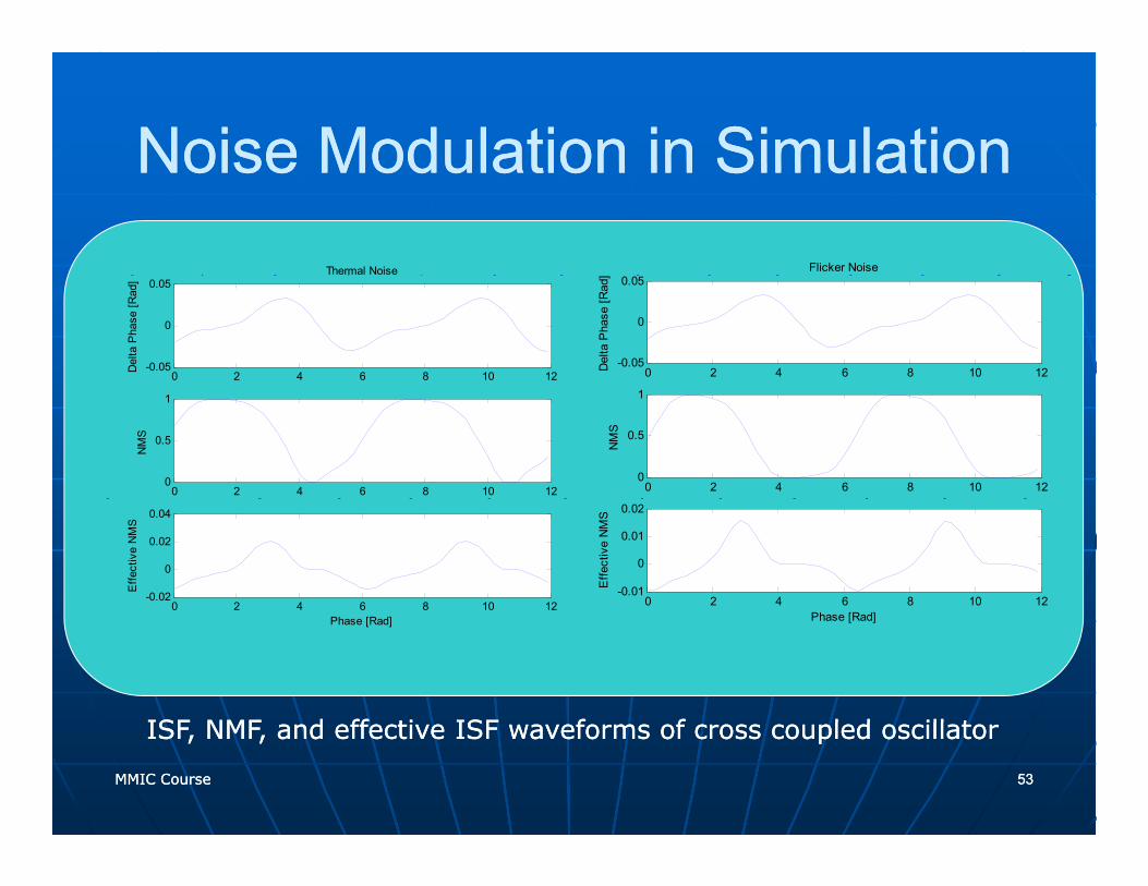
Noise Modulation in SimulationNoise Modulation in SimulationNoise Modulation in SimulationNoise Modulation in Simulation Thermal Noise Flicker Noise
0 2 4 6 8 10 12-0.05
0
0.05
Del
ta P
hase
[Rad
]
0 2 4 6 8 10 12-0.05
0
0.05
Del
ta P
hase
[Rad
]
0 2 4 6 8 10 120
0.5
1
NM
S
0 2 4 6 8 10 120
0.5
1
NM
S
0 2 4 6 8 10 12-0.02
0
0.02
0.04
Effe
ctiv
e N
MS
0 2 4 6 8 10 12-0.01
0
0.01
0.02
Effe
ctiv
e N
MS
Phase [Rad] Phase [Rad]
ISF NMF d ff ti ISF f f l d ill t ISF NMF d ff ti ISF f f l d ill t
MMIC CourseMMIC Course 5353
ISF, NMF, and effective ISF waveforms of cross coupled oscillator ISF, NMF, and effective ISF waveforms of cross coupled oscillator
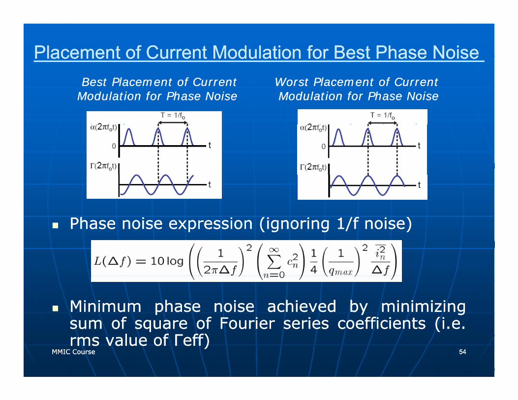
Placement of Current Modulation for Best Phase Noise Placement of Current Modulation for Best Phase Noise Best Placement of Current Best Placement of Current
Modulation for Phase Noise Modulation for Phase Noise Worst Placement of Current Worst Placement of Current Modulation for Phase NoiseModulation for Phase Noise
Phase noise expression (ignoring Phase noise expression (ignoring 11/f noise) /f noise) Phase noise expression (ignoring Phase noise expression (ignoring 11/f noise) /f noise)
Minimum phase noise achieved by minimizing Minimum phase noise achieved by minimizing sum of square of Fourier series coefficients (i e sum of square of Fourier series coefficients (i e
MMIC CourseMMIC Course 5454
sum of square of Fourier series coefficients (i.e. sum of square of Fourier series coefficients (i.e. rms value of Γeff) rms value of Γeff)
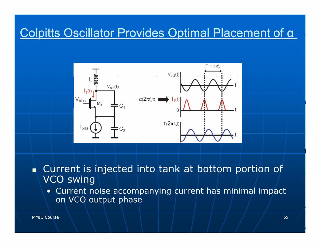
Colpitts Oscillator Provides Optimal Placement of α Colpitts Oscillator Provides Optimal Placement of α
Current is injected into tank at bottom portion of Current is injected into tank at bottom portion of VCO swing • Current noise accompanying current has minimal impact
on VCO output phase
MMIC CourseMMIC Course 5555
on VCO output phase
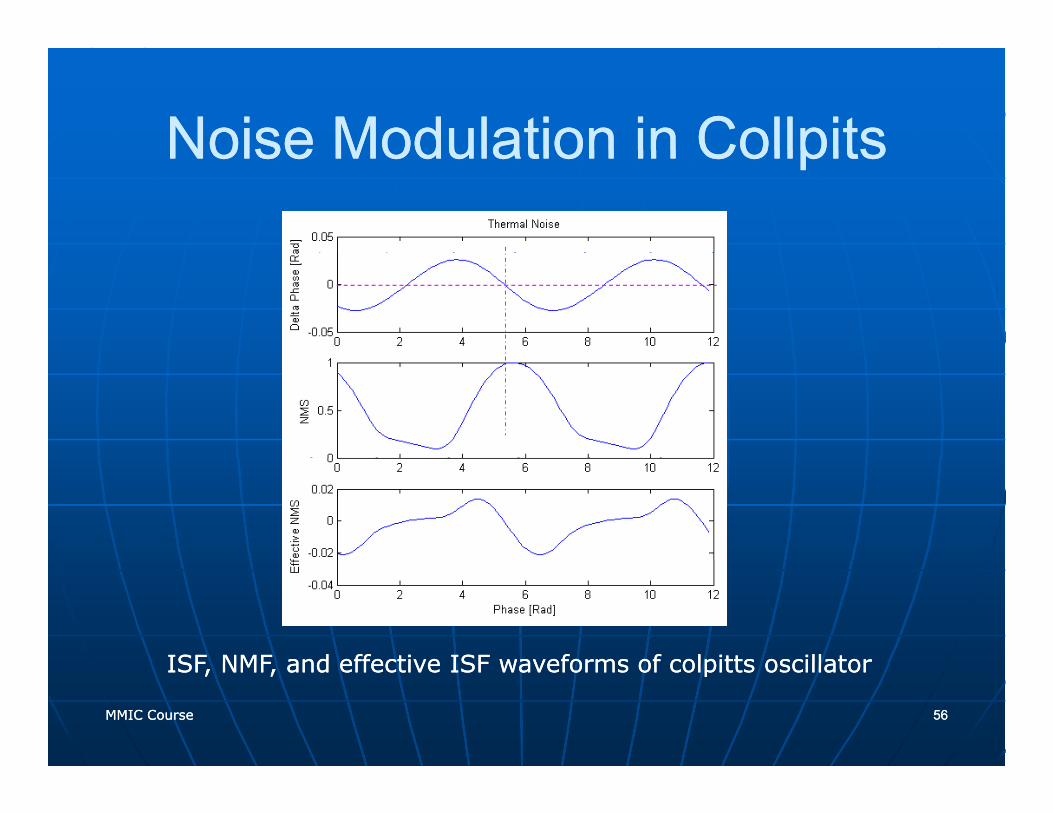
Noise Modulation in CollpitsNoise Modulation in CollpitsNoise Modulation in CollpitsNoise Modulation in Collpits
ISF NMF and effective ISF waveforms of colpitts oscillator ISF NMF and effective ISF waveforms of colpitts oscillator
MMIC CourseMMIC Course 5656
ISF, NMF, and effective ISF waveforms of colpitts oscillator ISF, NMF, and effective ISF waveforms of colpitts oscillator
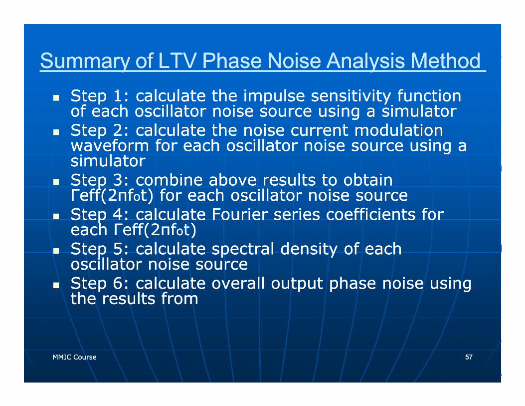
Summary of LTV Phase Noise Analysis Method Summary of LTV Phase Noise Analysis Method Step Step 11: calculate the impulse sensitivity function : calculate the impulse sensitivity function of each oscillator noise source using a simulator of each oscillator noise source using a simulator St St 22 l l t th i t d l ti l l t th i t d l ti Step Step 22: calculate the noise current modulation : calculate the noise current modulation waveform for each oscillator noise source using a waveform for each oscillator noise source using a simulator simulator Step Step 33: combine above results to obtain : combine above results to obtain Step Step 33: combine above results to obtain : combine above results to obtain Γeff(Γeff(22πfπfoot) for each oscillator noise source t) for each oscillator noise source Step Step 44: calculate Fourier series coefficients for : calculate Fourier series coefficients for each Γeff(each Γeff(22πfπfoot) t) each Γeff(each Γeff(22πfπfoot) t) Step Step 55: calculate spectral density of each : calculate spectral density of each oscillator noise sourceoscillator noise sourceStep Step 66 calc late o e all o tp t phase noise sing calc late o e all o tp t phase noise sing Step Step 66: calculate overall output phase noise using : calculate overall output phase noise using the results from the results from
MMIC CourseMMIC Course 5757
OutlineOutlineOutlineOutline
IntroductionIntroductionIntroductionIntroductionPhase NoisePhase NoiseO t t Ph N i S tO t t Ph N i S tOutput Phase Noise SpectrumOutput Phase Noise SpectrumOn chip InductorsOn chip InductorsAdvanced On Chip InductorAdvanced On Chip Inductor
MMIC CourseMMIC Course 5858
On chip InductorsOn chip InductorsOn chip InductorsOn chip InductorsIn contrast with digital circuits which use mainly In contrast with digital circuits which use mainly
ti d i ti d i hi i t hi i t active devices, onactive devices, on--chip passive components are chip passive components are necessary and imperative adjuncts to most RF necessary and imperative adjuncts to most RF electronics. These components include inductors, electronics. These components include inductors, capacitors varactors and resistors capacitors varactors and resistors capacitors, varactors, and resistors capacitors, varactors, and resistors For example, the Nokia For example, the Nokia 6161 6161 cellphone contains cellphone contains 15 15 IC’s with IC’s with 232 232 capacitors, capacitors, 149 149 resistors, and resistors, and 24 24 inductorsinductorsinductorsinductorsInductors in particular are critical components in Inductors in particular are critical components in low noise amplifiers, oscillators.low noise amplifiers, oscillators.The lack of an accurate and scalable model for The lack of an accurate and scalable model for The lack of an accurate and scalable model for The lack of an accurate and scalable model for onon--chip spiral inductors presents a challenging chip spiral inductors presents a challenging problem for RF IC’s designersproblem for RF IC’s designers
MMIC CourseMMIC Course 5959
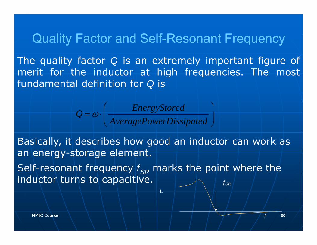
Quality Factor and SelfQuality Factor and Self--Resonant FrequencyResonant Frequencyyy yyThe quality factor Q is an extremely important figure ofmerit for the inductor at high frequencies. The mostg qfundamental definition for Q is
⎞⎛ edEnergyStor
B i ll it d ib h d i d t k
⎟⎟⎠
⎞⎜⎜⎝
⎛⋅=
ederDissipatAveragePowedEnergyStorQ ω
Basically, it describes how good an inductor can work as an energy-storage element. Self-resonant frequency f marks the point where the Self resonant frequency fSR marks the point where the inductor turns to capacitive.
LfSR
MMIC CourseMMIC Course 6060f
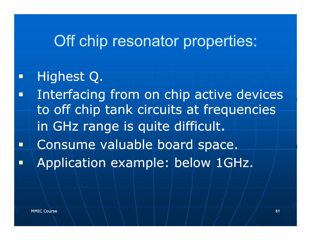
Off chip resonator properties:Off chip resonator properties:Off chip resonator properties:Off chip resonator properties:
Highest QHighest QHighest Q.Highest Q.Interfacing from on chip active devices Interfacing from on chip active devices
ff hi k i i f i ff hi k i i f i to off chip tank circuits at frequencies to off chip tank circuits at frequencies in GHz range is quite difficultin GHz range is quite difficult. . Consume valuable board space.Consume valuable board space.Application example: below Application example: below 11GHz. GHz. Application example: below Application example: below 11GHz. GHz.
MMIC CourseMMIC Course 6161
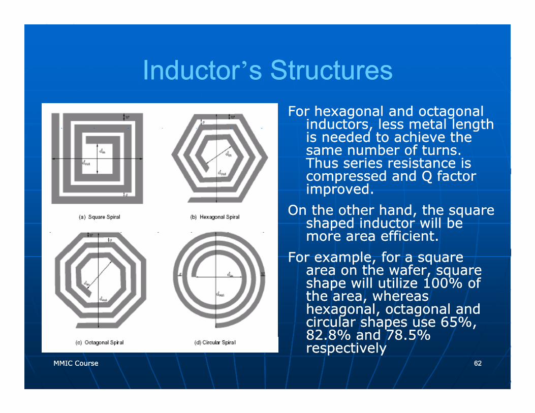
InductorInductor’’s Structuress StructuresInductorInductor s Structuress StructuresFor hexagonal and octagonal For hexagonal and octagonal
inductors, less metal length inductors, less metal length inductors, less metal length inductors, less metal length is needed to achieve the is needed to achieve the same number of turns. same number of turns. Thus series resistance is Thus series resistance is compressed and Q factor compressed and Q factor compressed and Q factor compressed and Q factor improved. improved.
On the other hand, the square On the other hand, the square shaped inductor will be shaped inductor will be
ffi i t ffi i t more area efficient. more area efficient. For example, for a square For example, for a square
area on the wafer, square area on the wafer, square shape will utilize shape will utilize 100100% of % of shape will utilize shape will utilize 100100% of % of the area, whereas the area, whereas hexagonal, octagonal and hexagonal, octagonal and circular shapes use circular shapes use 6565%, %, 8282 88% and % and 7878 55% %
MMIC CourseMMIC Course 6262
8282..88% and % and 7878..55% % respectively respectively
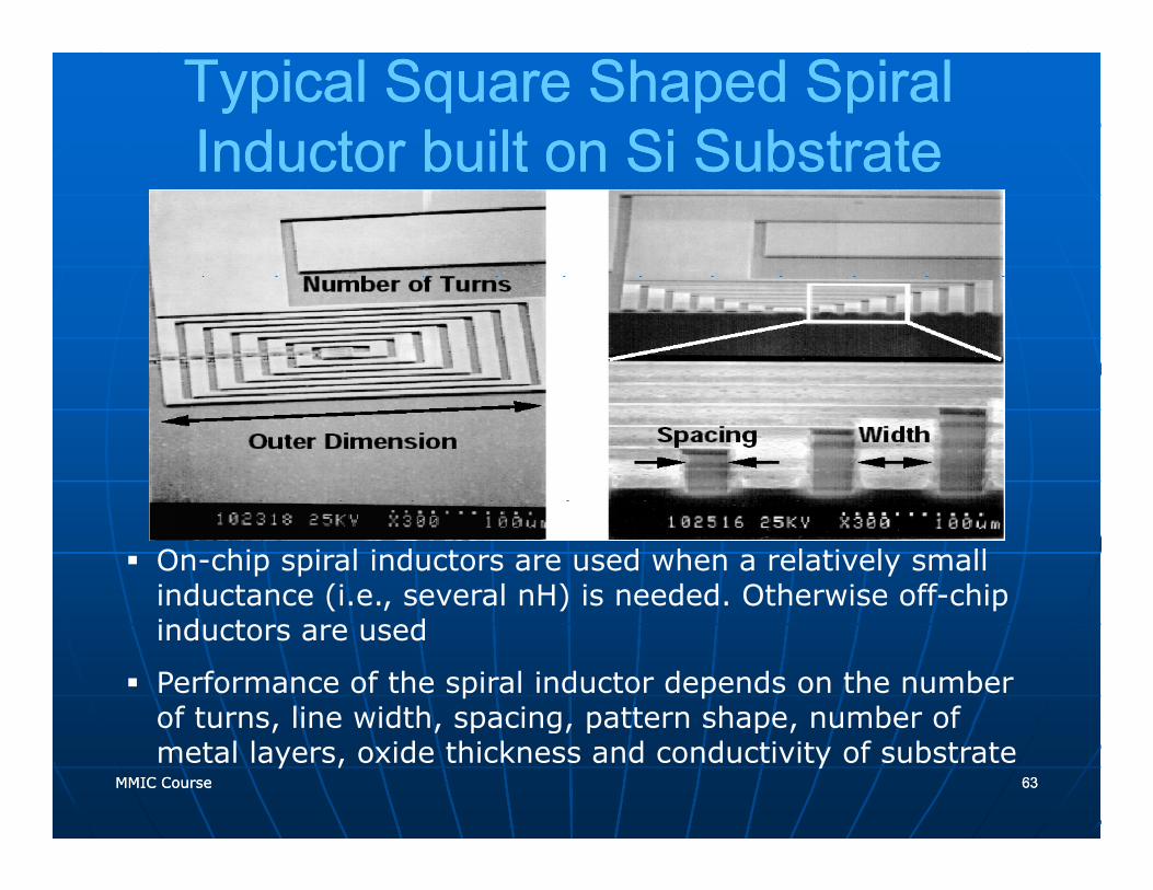
Typical Square Shaped Spiral Typical Square Shaped Spiral Inductor built on Si SubstrateInductor built on Si SubstrateInductor built on Si SubstrateInductor built on Si Substrate
On-chip spiral inductors are used when a relatively small inductance (i.e., several nH) is needed. Otherwise off-chip inductors are used
Performance of the spiral inductor depends on the number of turns, line width, spacing, pattern shape, number of
MMIC CourseMMIC Course 6363
of turns, line width, spacing, pattern shape, number of metal layers, oxide thickness and conductivity of substrate
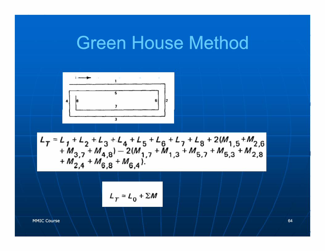
Green House MethodGreen House MethodGreen House MethodGreen House Method
MMIC CourseMMIC Course 6464
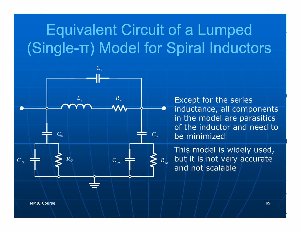
Equivalent Circuit of a Lumped Equivalent Circuit of a Lumped (Si l(Si l ) M d l f S i l I d t) M d l f S i l I d t(Single(Single--ππ) Model for Spiral Inductors) Model for Spiral Inductors
sC
Except for the series sL sR
s
Except for the series inductance, all components in the model are parasitics of the inductor and need to
s s
be minimized
This model is widely used, but it is not very accurate C R
oxC oxC
RC but it is not very accurate and not scalable
SiC SiRSiRSiC
MMIC CourseMMIC Course 6565
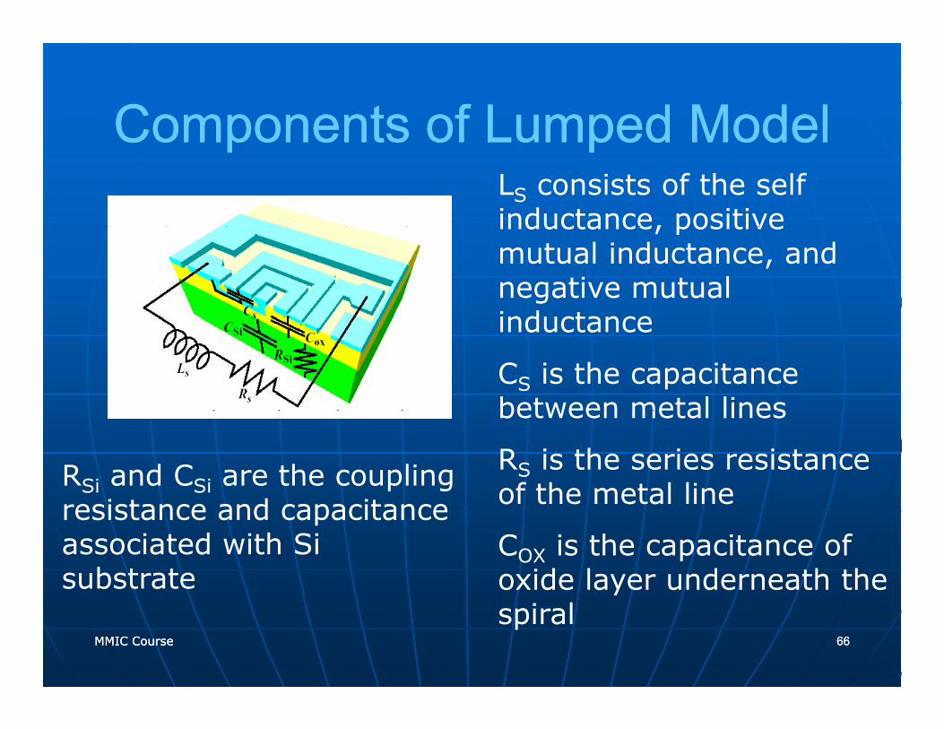
Components of Lumped ModelComponents of Lumped ModelComponents of Lumped ModelComponents of Lumped ModelLS consists of the self inductance, positive inductance, positive mutual inductance, and negative mutual inductanceinductance
CS is the capacitance between metal linesbetween metal lines
RS is the series resistance of the metal lineRSi and CSi are the coupling
i t d it of the metal line
COX is the capacitance of oxide layer underneath the
resistance and capacitance associated with Si substrate
MMIC CourseMMIC Course 6666
yspiral
OutlineOutlineOutlineOutline
IntroductionIntroductionIntroductionIntroductionPhase NoisePhase NoiseO t t Ph N i S tO t t Ph N i S tOutput Phase Noise SpectrumOutput Phase Noise SpectrumOn chip InductorsOn chip InductorsAdvanced On Chip InductorAdvanced On Chip Inductor
MMIC CourseMMIC Course 6767
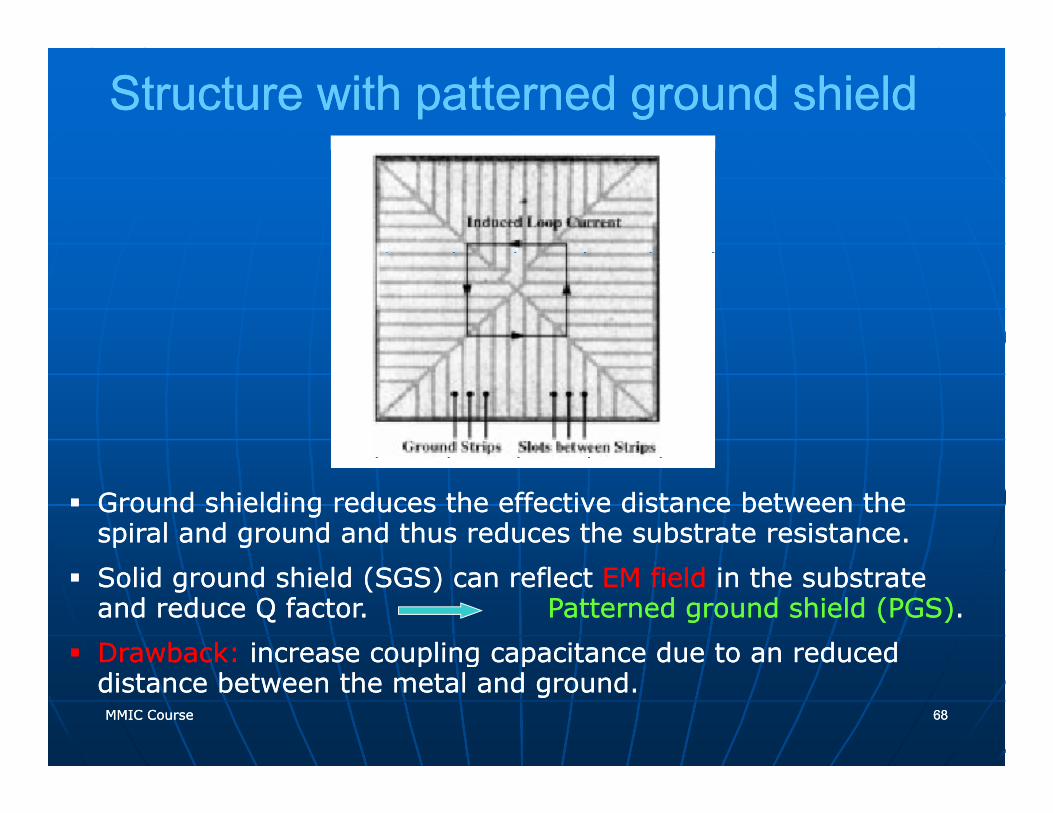
Structure with patterned ground shieldStructure with patterned ground shield
Ground shielding reduces the effective distance between the Ground shielding reduces the effective distance between the spiral and ground and thus reduces the substrate resistance. spiral and ground and thus reduces the substrate resistance.
Solid ground shield (SGS) can reflect Solid ground shield (SGS) can reflect EM fieldEM field in the substrate in the substrate and reduce Q factor. and reduce Q factor. Patterned groundPatterned ground shield (PGS)shield (PGS). .
Drawback:Drawback: increase coupling capacitance due to an reduced increase coupling capacitance due to an reduced
MMIC CourseMMIC Course 6868
p g pp g pdistance between the metal and ground. distance between the metal and ground.
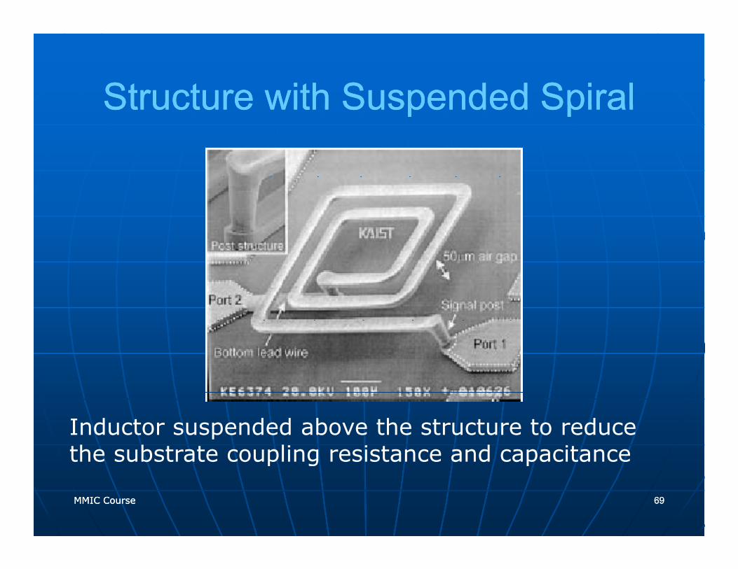
Structure with Suspended SpiralStructure with Suspended SpiralStructure with Suspended SpiralStructure with Suspended Spiral
Inductor suspended above the structure to reduce the substrate coupling resistance and capacitance
MMIC CourseMMIC Course 6969
p g p
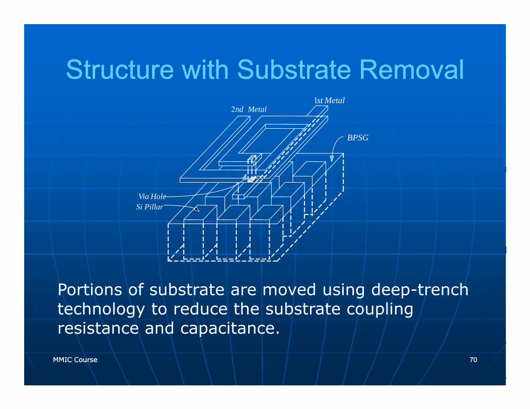
Structure with Substrate RemovalStructure with Substrate RemovalStructure with Substrate RemovalStructure with Substrate Removalst1 Metal
nd2 Metal
BPSG
Via HoleSi Pillar
Portions of substrate are moved using deep-trench technology to reduce the substrate coupling resistance and capacitance.
MMIC CourseMMIC Course 7070
resistance and capacitance.
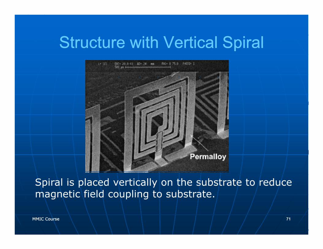
Structure with Vertical SpiralStructure with Vertical SpiralStructure with Vertical SpiralStructure with Vertical Spiral
Spiral is placed vertically on the substrate to reduce magnetic field coupling to substrate.
MMIC CourseMMIC Course 7171
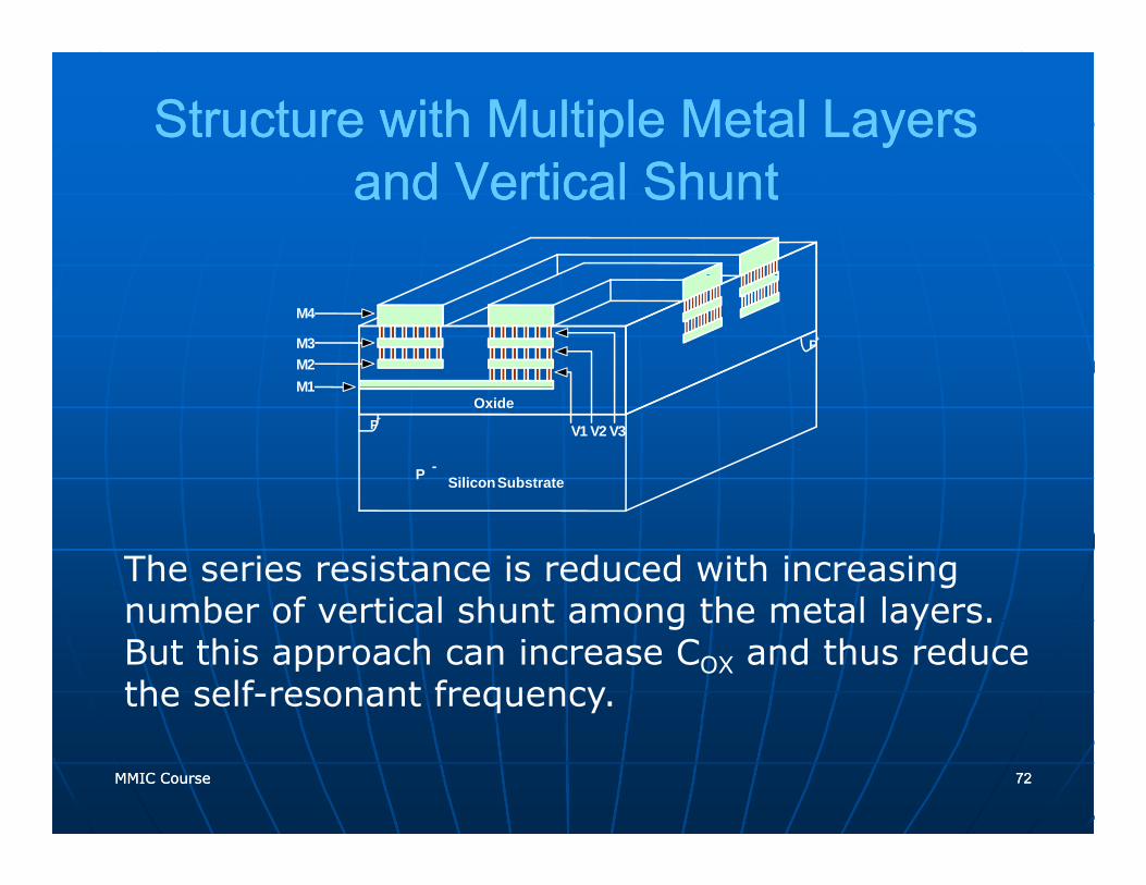
Structure with Multiple Metal Layers Structure with Multiple Metal Layers d V ti l Sh td V ti l Sh tand Vertical Shuntand Vertical Shunt
M4
M3M2M1
P+
M1
V1 V2 V3
OxideP+
P -SiliconSubstrate
The series resistance is reduced with increasing number of vertical shunt among the metal layers number of vertical shunt among the metal layers. But this approach can increase COX and thus reduce the self-resonant frequency.
MMIC CourseMMIC Course 7272
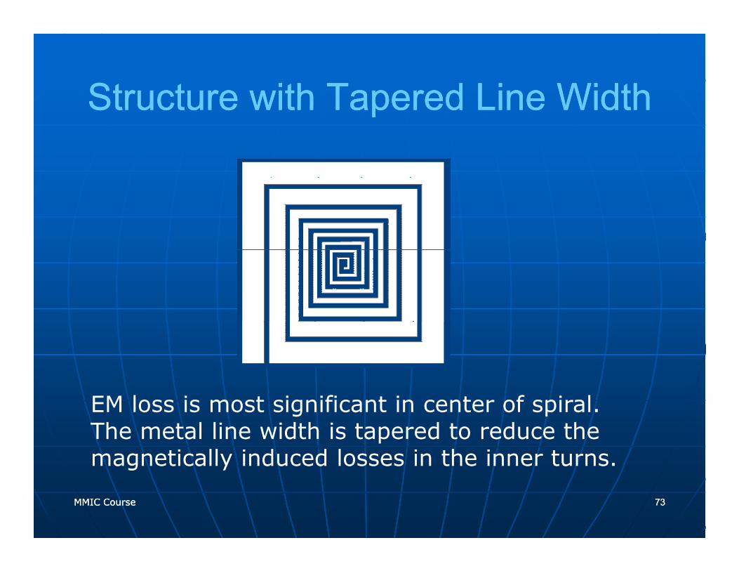
Structure with Tapered Line WidthStructure with Tapered Line WidthStructure with Tapered Line WidthStructure with Tapered Line Width
EM loss is most significant in center of spiral. The metal line width is tapered to reduce the magnetically induced losses in the inner turns.
MMIC CourseMMIC Course 7373
magnetically induced losses in the inner turns.
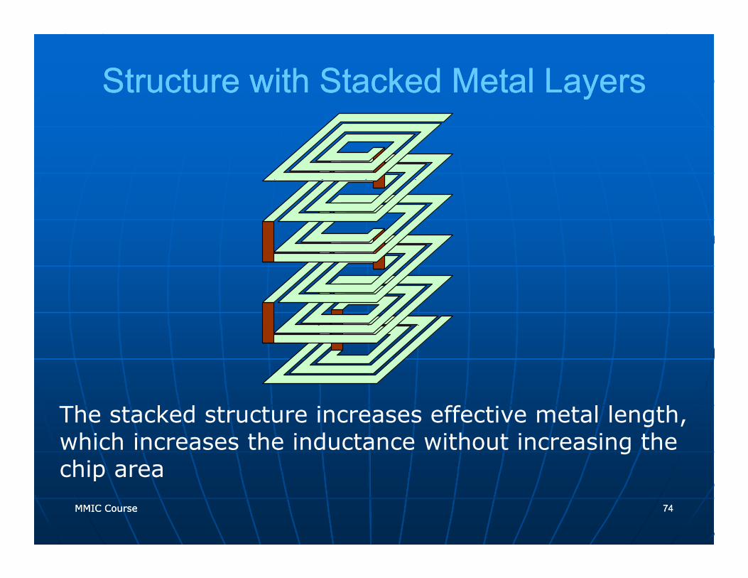
Structure with Stacked Metal LayersStructure with Stacked Metal Layers
The stacked structure increases effective metal length, which increases the inductance without increasing the chip area
MMIC CourseMMIC Course 7474
chip area
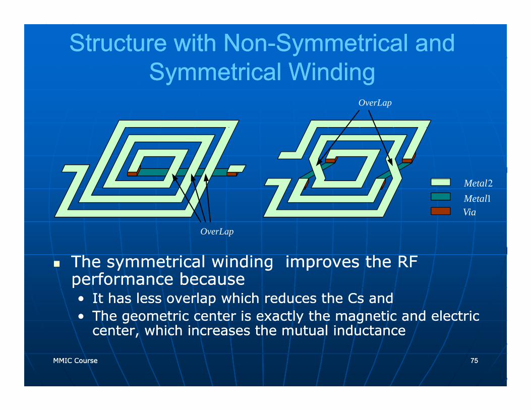
Structure with NonStructure with Non--Symmetrical and Symmetrical and Symmetrical WindingSymmetrical WindingSymmetrical WindingSymmetrical Winding
OverLap
1Metal2Metal
Via
OverLap
The symmetrical winding The symmetrical winding improves the RF improves the RF performance because performance because
OverLap
performance because performance because •• It has less overlap which reduces the Cs and It has less overlap which reduces the Cs and •• The geometric center is exactly the magnetic and electric The geometric center is exactly the magnetic and electric
center, which increases the mutual inductance center, which increases the mutual inductance
MMIC CourseMMIC Course 7575
center, which increases the mutual inductance center, which increases the mutual inductance
Future WorksFuture WorksFuture WorksFuture Works
Intrinsic Mesfet noisesIntrinsic Mesfet noisesIntrinsic Mesfet noisesIntrinsic Mesfet noisesPhase noise in different topologyPhase noise in different topologyI d t i G A I d t i G A Inductors in GaAs Inductors in GaAs
MMIC CourseMMIC Course 7676
ReferencesReferencesReferencesReferences1.1. Hajimiri and T. Lee, “A general theory of phase noise in Hajimiri and T. Lee, “A general theory of phase noise in
electrical oscillators ” IEEE J Solidelectrical oscillators ” IEEE J Solid State Circuits vol State Circuits vol 3333 electrical oscillators, IEEE J. Solidelectrical oscillators, IEEE J. Solid--State Circuits, vol. State Circuits, vol. 3333, , pp. pp. 179179––194194, Feb. , Feb. 19981998..
2.2. 11Roberto Aparicio and Ali Hajimiri, "A NoiseRoberto Aparicio and Ali Hajimiri, "A Noise--Shifting Shifting Differential Colpitts VCO," IEEE,Differential Colpitts VCO," IEEE,20022002..
3.3. Thomas H. Lee, Member, IEEE, and Ali Hajimiri , Thomas H. Lee, Member, IEEE, and Ali Hajimiri , "Oscillator Phase Noise: A Tutorial", Member, IEEE, "Oscillator Phase Noise: A Tutorial", Member, IEEE, 20002000..
4.4. Hajimiri and T. Lee , “Design issues in CMOS differential Hajimiri and T. Lee , “Design issues in CMOS differential LC oscillators ” IEEE J SolidLC oscillators ” IEEE J Solid--State Circuits vol State Circuits vol 3434 pp pp LC oscillators, IEEE J. SolidLC oscillators, IEEE J. Solid State Circuits, vol. State Circuits, vol. 3434, pp. , pp. 716716––724724, May , May 19991999..
5.5. Razavi , “A study of phase noise in CMOS oscillators,” Razavi , “A study of phase noise in CMOS oscillators,” IEEE J. SolidIEEE J. Solid--State Circuits, vol. State Circuits, vol. 3131, pp. , pp. 331331––343343, Mar. , Mar. 1996199619961996..
MMIC CourseMMIC Course 7777
Recommended