\
CALIFORNIA INSTITUTE OF TECHNOLOGY
OPTIMUM NOISE PERFORMANCE
OF TRANSISTOR INPUT CIRCUITS
by R. D. Middlebrook
TRANSISTOR AC AND DC AMPLI Fl E RS
WITH HIGH INPUT IMPEDANCE
by R. D. Middlebrook and C. A. Mead
Ca"for •
.r f l e c r t" J rw!ogy E t.: b cc.. Er:gineer rg
Libra~
Electrical Engineering Department March 1959

OP.riMUM NOISE PERFORMAh0E
OF TRANSISTOR INPUT CIRCUITS
by
R. D. Middlebrook
Presented at the Philadelphia Transistor and Solid State Circuits Conference,
February 1958.
Published in Semiconductbr Products, July7August, 1958 .
..;antnrma
tnst·"·~ p • • • :· noivgy
Libra.y
TRANSISTOR AC AND DC AMPLIFIERS
WITH HIGH INPUT IMPEDANCE
by
R. D. Middlebrook and c. A. Mead
Published in Semiconductor Products, March 1959·
•
OP.l'IMUM NOISE PERFORMANCE OF TRANSISTOR INPUT CIRCUITS
ADS TRACT
Same results are presented for optimum noise performance of tran-
sistor input stages when fed from resistive or reactive sources.
Standard theory has shown that a common-emitter transistor fed from a
resistive source presents a minimum noise figure F when the source m
resistance has a certain value Rf!'Pl in the order of lkn· In this
paper, expressions are developed for minimum noise figure and optimum
source resistance in the presence of base bias resistors, emitter de-
generation resistance, and various kinds of feedback. Results are in
terms of F and R only, and do not contain other functions of the m fYil
transistor internal noise sources. It is shown that the minimum noise
figure is never less than F , but the optimum source resistance can be m
either greater or less than R gpl
In the case of reactive sources, noise figure is meaningless and
the quantity of interest is signal-to-noise ratio over the passband.
It is shown that for an inductive source, such as a magnetic tape head,
there is a maximum signal-to-noise ratio obtainable with an optimum
source inductance, and that a Figure of Merit can be assigned to the
source which is independent of its inductance .
Experimental results presented for both resistive and inductive
sources show good agreement with the theoretical predictions.

Page 1
I. Introduction
The noise performance of any electronic circuit, whether measured in
terms of noise figure or signal-to-noise ratio, is dependent on two classes
of properties: first, the physical sources of noise within the circuit
components, and second, the way in which the components are interconnected.
This paper is concerned with the second of these, and in particular, with
the effects on the overall noise performance of various circuit arrange-
mente of transistors and passive elements with given noise properties.
1 It has been shown by Bargellini and Herscher that a transistor fed
from a resistive source exhibits a noise figure F which is a function of
the transistor internal parameters and noise sources and of the. external
signal source resistance
exhibits a minimum value
R . It was also shown that the noise figure g
F when the source resistance has an optimum m
value R in the order of lkn, and that the values of F and R ~ m ~
are essentially the same whether the transistor is in CE, CB, or CC con-
nection.
It will be shown in the following work that the noise figure of a cir-
cuit containing aCE transistor and a resistive signal source exhibits a
minimum noise figure F I m
for an optimum source resistance R ~
in the
presence of bias resistors, emitter degeneration resistors, and feedback.
Expressions for F I
m and R gm
are presented in terms of F m
and R ~
as defined above. It will be shown that F 1 is always equal to or greater m
than F , and that m R~ may be either greater than or less than R
~
However, it is easy to design circuits in which
a small amount.
F I
m exceeds F by only
m
In many practical applications the signal source feeding a transistor
amplifier is not purely resistive. In these circumstances the noise perfo~-
ance of the entire circuit is more conveniently expressed in terms of signal~
to-noise ratio at the output rather than in ter.ms of noise figure. Indeed,
Page 2
noise figure becomes meaningless if the signal source is purely reactive, a
condition approximated in magnetic tape heads. It is obvious that the
noise perfonnance in such cases is intimately connected not only with the
properties of the transistor and associated circuitry, but also with the
properties of the signal source or transducer.
Since the design of transistor amplifiers to be fed from magnetic tape
heads or other inductive sources is of some practical importance, it is of
interest to inquire whether an optimum source inductance exists which
would maximize the output signal-to-noise ratio of the whole circuit. It
will be shown in the following work that under certain condi tiona an opti
mum source inductance does in fact exist, and expressions for this quantity
and for the maximum attainable signal-to-noise ratio will be given. These
expressions are in a convenient fonn for practical use, since they are in
tenns of quanti ties easily measurable or calculable from the noise proper
ties of the first-stage transistor, the overall gain versus frequency
characteristic, and certain circuit parameters concerned with the biasing
arrangements of the first-stage transistor. It will further be shown that
a Figure of Merit can be ascribed to an inductive signal source, to which
the signal-to-noise ratio of the complete amplifier is proportional. Ex
perimental results pre~ented for both resistive and inductive sources show
good agreement with the theoretical predictions.
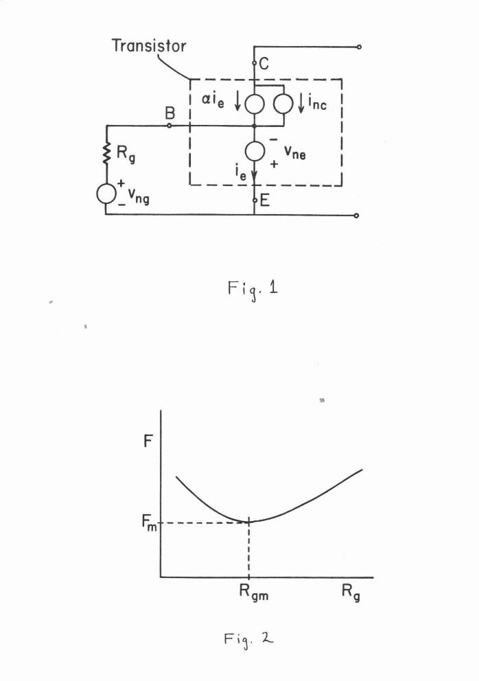
II. Amplifier Noise Figures with Resistive Sources
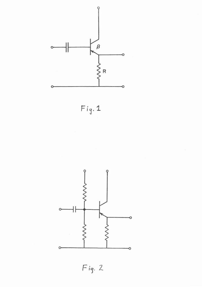
The equivalent circuit to be used to represent a noisy transistor is
shown in Fig. 1. This representation is stripped to the bare essentials
since the present concern is with the circuit properties of the transistor
and not with its internal performance. The simpler the equivalent circuit
of the transistor, the simpler and more illuminating will be the desired
results, and the justification for such simplicity will be found in the
Page 3
validity of the results for practical purposes. Thus in the tee equivalent
circuit of Fig. 1, the emitter and base resistances are assumed negligibly
small , the collector resistance negligibly large, and frequencies of
interest are assumed to be such that collector capacitance and variations of
the current gain a may be ignored. The internal mechanisms of noise
generation are here of no interest, and the simplest valid representation
of the noise is by means of an emitter noise voltage generator v ne and a
collector noise current generator i nc The polarities shown in Fig. 1 are
of course arbitrary, since ultimately only noise powers are of interest.
The quantities vne and i nc
are defined as rms noise voltage and current
in 1 cps bandwidth, and in the present work are considered to be the same
at all frequencies; thus "1/f noise" is neglected. However, this limita-
tion is not necessary, and the principles of most of the calculations des-
cribed herein are equally valid if this restriction is removed, although
the complexity of the results is considerably increased.
For future purposes, it is convenient to suppose that the emitter noise
voltage is due to a fictitious "emitter effective noise resistance" R dene
fined by v 2 = 4kTR , where k is Boltzmann's constant and T is the ne ne
absolute temperature.
If a noisy transistor is connected as a CE amplifier to a signal source
of internal resistance R , and thermal noise voltage v g ng (4kTR )1/ 2 in
g
1 cps bandwidth, as in Fig. 1, it is easily shown that the noise figure F
of the circuit is given by
F (1)
The noise figure is therefore a function of the generator resistance Rg'
and exhibits a minimum value F when the generator resistance has an m

Page 4
optimtml value Rgm' where
av ne
Rgm = -i-nc
2R l+~
R gm
(2)
( 3)
l The above equations may be obtained from the work of Bargellini and Herscher
by appropriate simplification .
Figure 2 shows the general form of the variation of the noise figure
F as a function of the generator resistance Rg for the circuit of Fig. 1.
For a low-noise transistor, F is of the order of 2.5 (4 db) and R m gm
in the region of J.kn, These two quanti ties are readily measured, and fran
them the parameters vne' i ' nc and R can be determined fran Eqs. ( 2)
ne
and ( 3) . From the applications point of view, the circuit measurements are
more appropriate than the internal generators v and i nc' and hence in ne
the following work r esults will be expressed in terms of F and R m gm
Practical transistor amplifiers are rarely as simple as that shown in
Fig. 1. It is, therefore, of interest to consider the effects on noise per-
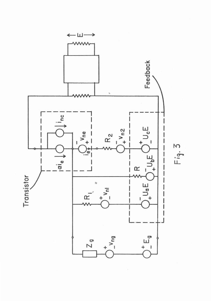
formance of typical associated circuitry. Figure 3 shows the equivalent
circuit of a generalized transistor amplifier input stage which contains
most of the features likely to be encountered in a realistic amplifier: the
input signal voltage E may arise in a reactive source of impedance g
Z = R + JX and with thermal noise v = (4kTR )1
/ 2. the resistor R1 g g g ng g ,
and its thermal noise vnl = (4kTR1 )1
/ 2 accounts for any biasing arrange-
ment to the base of the first-stage transistor, such as
divider; the resistor R2 and its thermal noise v = n2
the usual potential
(4kTR )1
/ 2 accounts 2
for any emitter degeneration caused by un-bypassed emitter resistance; and
Page 5
the generators u ' a and U
c account, respectively, for bias resistor
bootstrapping, feedback to the base, and feedback to the emitter, all pro-
portional to the complete amplifier output voltage E. It is assumed that
all noise sources following the first-stage transistor may be neglected.
Let it first be supposed that the signal source is purely resistive,
thus X = 0. The noise figure F' of the complete amplifier may be cang
puted with greater complexity than difficulty, and is found to show a mini-
mum value F 1 when the source resistance has an optimum value R 1• These
m ~
quantities may be expressed in terms of the corresponding quantities
Rgm for the simple CE transistor (defined above) as
F m and
R ' gm
[
1 + (R/Rgm) 2 + R2/~e ll/2
= -(l_+_R_2_/R_l_)-:::"2 ~+-=-( R_gm_/_R_l-:) 2::----:+=(~l-+-R2-/-~-)-R-~..._.,2,...../-~-R-ne-) J (4) R
gm
F ' - 1 m
F - 1 m
(5)
Although interpretation of the above equations is somewhat laborious, one
conclusion is immediately obvious: neither R gm nor F ' depends on any
m
of the feedback generators U. The importance of this result may be emphasized
by stating it in other words: the input impedance and the gain characteristic
of the amplifier are strongly dependent on any feedback, but the minimum
noise figure attainable and the optimum source resistance to provide it are
unaltered by feedback and remain the same as when no feedback is applied.
It is seen from Eqs. (4) and (5) that the only elements causing R 1
~
and Fm 1 to differ from Rgm and Fm are the resistors !)_ and R2• In
order to obtain a clearer understanding of their effects, it is convenient
to consider the modifications introduced by R1 and R2
separately. If,
first, R2
= 0, Eqs. (4) and (5) reduce to
Rgm =
R I
gm [
R@}ll 2 ( !)_ )] 1 / 2 1+-- 1+-
R 2
R 1 ne
F 1
- 1 (1 1 ) Fm- 1 = R R + ~ m gm 1 E911
Page 6
(6)
(7)
It is seen from the above results that R 1 ~ R and F '~F, that is, gm gm m m
the presence of R1 always increases the minimum noise figure and decreases
the optimum source resistance necessary to achieve i t.
If, next, R1 = oo, Eqs. (4) and (5) reduce to
Rgm I
(1 R 2 R ) 1/2
--= +-2-+~ R R 2 R gm gm ne
(8)
F I - 1 1 m
(R 2 + Rgm 1) F - 1
=-R m gm
(9)
from which it is seen that R 1 ~ R and F 1 ~ F , that is, the presence gm gm m m
of R2
always increases the minimum noise figure and increases the optimum
source resistance necessary to achieve it .
The similarity between the pairs of equations (6), (7), and (8), (9)
suggests that a single graph with appropriate variables could be drawn for
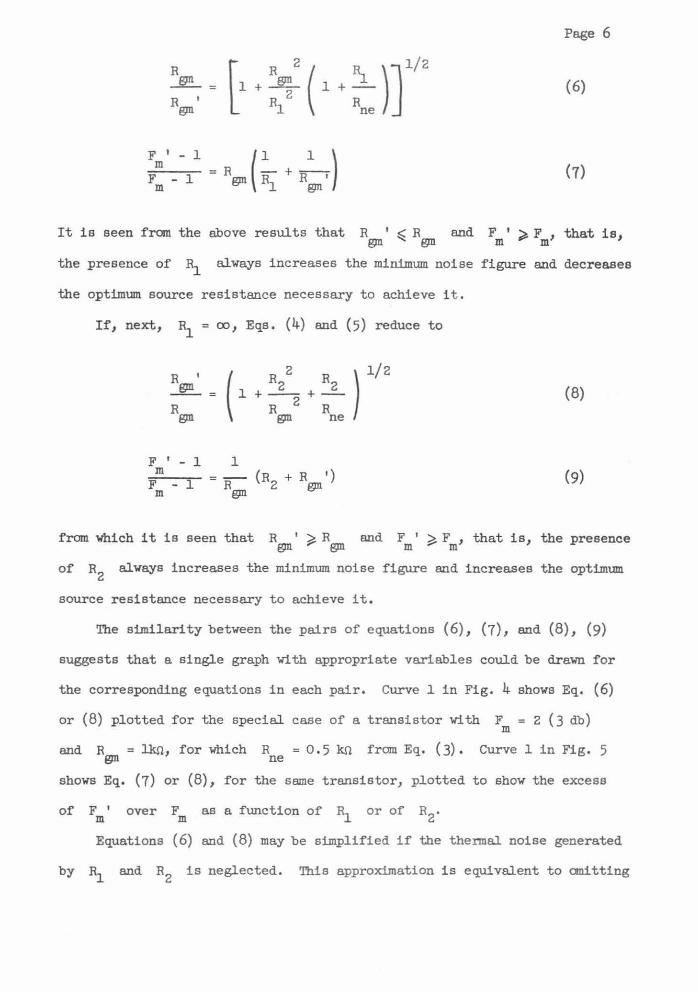
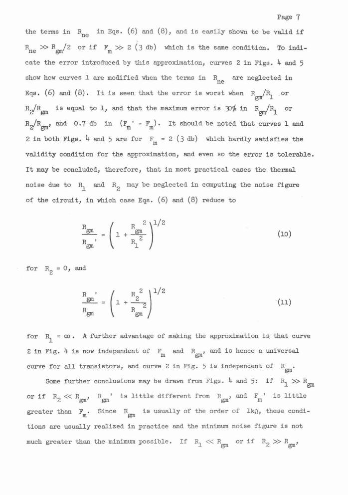
the corresponding equations in each pair. Curve 1 in Fig. 4 shows Eq. (6)
or (8) plotted for the special case of a transistor with F = 2 (3 db) m
and R = l.kn, for which R = 0. 5 kn from Eq. ( 3). Curve 1 in Fig. 5 gm ne
shows Eq. (7) or (8), for the same transistor, plotted to show the excess
of Fm 1 over Fm as a function of R1 or of R2.
Equations (6) and (8) may be simplified if the thermal noise generated
by ~ and R2
is neglected. This approximation is equivalent to anitting
Page 7
the terms in R in Eqs. (6) and (8), and is easily shown to be valid if ne
Rne >> Rf!Jil/2 or if Fm >> 2 (3 db) which is the same condition. To indi-
cate the error introduced by this approximation, curves 2 in Figs. 4 and 5
show how curves 1 are modified when the terms in R are neglected in ne
Eqs. (6) and (8). It is seen that the error is worst when Rgm/R1
or
R/Rgm is equal to 1 1 and that the maximum error is J)cf, in Rgm/~ or
R/Rgm' and 0. 7 db in (Fm' - Fm). It should be noted that curves 1 and
2 in both Figs. 4 and 5 are for F m
2 ( 3 db) which hardly satisfies the
validity condition for the approximation, and even so the error is tolerable.
It may be concluded, therefore, that in most practical cases the thermal
noise due to R1
and R2
may be neglected in computing the noise figure
of the circuit, in which case Eqs. (6) and (8) reduce to
( R 2 )1/2
= 1 +7 Rl
(10)
for R2
= 0, and
(11)
for ~ = a>. A further advantage of making the approximation is. that curve
2 in Fig. 4 is now independent of F and R , and is hence a universal m gm
curve for all transistors, and curve 2 in Fig. 5 is independent of R • gm
Some further conclusions may be drawn from Figs . 4 and 5: if R1 >> Rgm
R gm is little different from R , and F ' is little gm m
greater than F • Since R is usually of the order of lkn, these condi-m gm
tiona are usually realized in practice and the minimum noise figure is not
much greater than the minimum possible. If R1 << Rgm or if R2 >> Rgm'

Page 8
R tends to R1 or to R2
as appropriate, and the minimum noise figure grn
is appreciably greater than the minimum possible. Further, as shown in
curves 3 and 4 of Fig. 5, the greater the value of F for the transistor, m
the greater is the increase above F m in the noise figure of the complete
circuit.
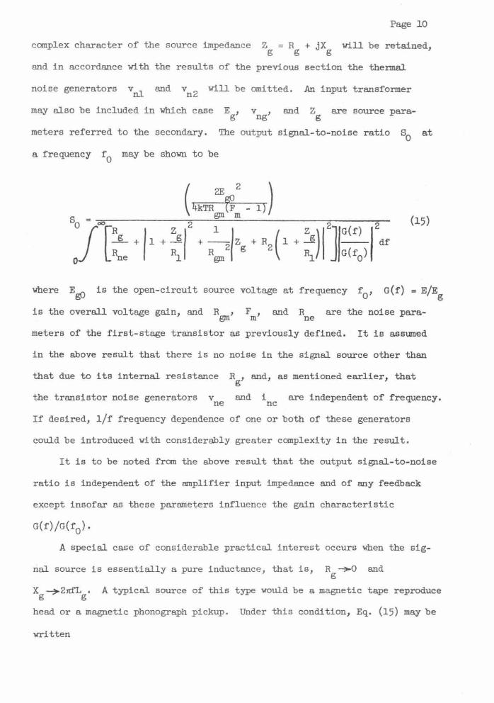
To check the validity of the results described, experimental measure-
menta of the 1 kc noise figure were made for various values of R1
and
R2 and compared with the predicted values. The procedure was as follows.
Measurements of the noise figure F of a single CE transistor as shown i n
Fig. 1 wer e made as a function of source resistance
should satisfy the relation
F (F - 1) (R - R ) 2
F + _m--=-- --=g=-=--=gm'---m 2 R R
ggm
R • g
These poi nts
(12)
The line shown in Fig. 6 (for ~ = co ) or in Fig. 7 (for R2 = 0 ) is the
best fit with the experimental points which also satisfies Eq. (12) . From
this ''best fit" line, the values of F and R for the experimental m gm
transistor at the particular operating point chosen were found to be
F m
5.62 (7. 5 db) and R = 0.63 kn· • gm
In the presence of R1
, the noise figure F' as a function of source
resistance Rg should satisfy the relation
(13)
where Fm' and Rgm are given by Eqs. (7) and (10) respectively. Figure
6 shows Eq. (13) plotted for three values of R1 , and it is seen that the
experimental points agree quite well with the predicted curves. It should
be noted that thermal noise in R1 was neglected in computing the curves,

Page 9
and the agreement between the measured and predicted results is further
evidence of the validity of the approximation.
In the presence of R2, the noise figure F' as a function of source
resistance R should satisfy the relation g
(14)
where F ' and R m g)ll
are given by Eqs. (9) and (11) respectivel y . Figure
7 shows Eq. (14) plotted for two values of R2, and again the agreement be
tween measured and predicted results is good even though thermal noise in
R2
is neglected.
III. Amplifier Signal-to-Noise Ratios with Reactive Sources
If the signal source impedance contains a reactive component, the spot
noise figure of the complete amplifier will vary with frequency. Indeed, if
the source is purely reactive, noise figure becomes meaningless . In such
cases a more useful measure of noise performance is the s i gnal- to-noise ratio
s0 at the amplifier output. More precisely, s0 may be defined as the
ratio of the signal power in the load to the total noise power in the load.
In general, the signal power in the load will depend on the chosen frequency
f0
, the source voltage at r0 , and the overall amplifier gain at f0
• The
total noise power in the load will depend on the noise properties of the
first-stage transistor and associated circuit elements, any noise from the
signal source such as its own resistive thermal noise and noise brought into
the system along with the signal, and on the overall gain versus frequency
response of the complete amplifier.
The equivalent circuit of the generalized amplifier shown in Fig. 3
will again provide a sui table foundation for discussion, except that the
Page 10
complex character of the source impedance Z = R + jX will be retained, g g g
and in accordance with the results of the previous section the thermal
noise generators vnl and vn2
will be omitted. An input transformer
may also be included in which case E ' g and zg are source para-
meters referred to the secondary. The output signal-to-noise ratio s0
at
a frequency f0
may be shown to be
(15)
where EgO is the open-circuit source voltage at frequency f0
, G(f) = E/E g
is the overall voltage gain, and R , F 1 and R are the noise para-gm m ne
meters of the first-stage transistor as previously defined. It is assumed
in the above result that there is no noise in the signal source other than
that due to its internal resistance R , and, as mentioned earlier, that g
the transistor noise generators v ne and i
nc are independent of frequency.
If desired, 1/f frequency dependence of one or both of these generators
could be introduced with considerably greater complexity in the result.
It is to be noted from the above result that the output signal-to-noise
ratio is independent of the amplifier input impedance and of any feedback
except insofar as these parameters influence the gain characteristic
A special case of considerable practical interest occurs when the sig-
nal source is essentially a pure inductance, that is, R --:'>-0 and g
X ~21tf'L • A typical source of this type would be a magnetic tape reproduce g g
head or a magnetic phonograph pickup. Under this condition, Eq. (15) may be
written

in which M is a "source parameter" defined as
'\ and A2
are "gain parameters" defined by
and c1 and C 2 are "circuit parameters" defined by
c = 2 [ (
R ) 2 R 2 J 1/2 1+~ +~
2 Rl Rl
Page 11
(16)
(17)
(18)
(19)
( ro)
(21)
Some properties of the "source parameter" M are of interest. Con-
sider a magnetic tape head containing N turns of wire of negligible re-
sistance . If the head is stimulated by a tape recorded with constant flux
amplitude at all frequencies ¢ = r sin 2~ ft, then the open-circuit volt
age of the head will be proportional to the frequency and to the number of
•
Page 12
turns:
( 22)
However, the inductance of the head is proportional to the square of the
number of turns:
( 23)
The above relations assume no leakage flux and that the head gap is small
compared to the recorded wavelength. It follows from Eqs . (22) and (23)
2 2 that the quantity E /f L is independent of frequency and the number of
g g
turns, and hence of the inductance, if the tape is recorded with constant
flux amplitude. Similarly, for a phonograph pickup the same remarks apply
if the disk recording characteristic is constant amplitude at all frequen-
cies. Even if the recording characteristic is not constant amplitude,
E 2jf~ is still independent of the inductance though not of frequency.
g
It follows, therefore, that the "source parameter" M may be rewritten
E 2 M = g
8nkTf\ g
( 24)
and may be rechristened a Figure of Merit for the source "Which is independent
of its inductance and also, in certain circumstances, of frequency. A de-
finition of the Figure of Merit in physical terms may be expressed as
follows:
M 2(max. available signal energy in 1 cycle)
thermal energy in 1 cycle
•
Page 13
The source Figure of Merit is a dimensionless number which may for con-
venience be expressed in db.
Attention may now be returned to Eq. (16). The output signal-to-noise
ratio is seen to be a function of the source inductance L , and since g
it has been shown that M is independent of L g
it follows that S ex-0
hibits a maximum value 80m When the source inductance has an optimum
value L , where, from Eq. (16) gill
L gill
M
(25)
(26)
The optimum source inductance Lgm is, of course, independent of the fre
quency f0
at Which s0
is determined, while s0
is not, in general, in
dependent of f0
•
It has thus been shown that an optimum source inductance exists for
which a maximum output signal-to-noise ratio is realized, and expressions
for these two quantities have been given in terms of a source Figure of
Merit, the first-stage transistor noise parameters Fm and R , amplifier gm
overall gain parameters, and circuit parameters containing only the resis-
tors ~ and R2
shown in Fig. 3. The results are easily applied to
practical design problems to determine the maximum attainable signal-to-
noise ratio and the required source inductance. For a given source, it is
of course usually more convenient to match the existing source inductance to
the optimum value by a transformer than to redesign the transducer.
Some typical figures will help to give insight into the magnitudes in-
volved. Suppose a transistor amplifier is to be designed to provide constant
output at all frequencies between f1 = 50 cps and f 2 = 10 kc from a

Page 14
magnetic tape recording. It is desired to find the maximum attainable
signal-to-noise ratio and the optimum source inductance given that the
first stage transistor has F m 4 (6 db), R = l.kn, and that the tape gm
head has an inductance of 3 mh and provides an output of 0. 6 mv at
1 kc.
Insertion of the given figures for the tape head into Eq. (24) leads
to a value for the Figure of Merit of M = 1.2 x 10⁹ (91 db). It remains
only to find the "circuit parameters" and the "gain parameters". To take
a case 'WOrse than 'WOuld probably occur in practice, suppose that in the
circuit of Fig. 3 ~ = 5kn and R2 = lkn. Use of Eqs. (~) and (21) leads
to cl = 1.41, c2 = 1. 22 (note that cl = c2 = 1 if ~ = 00 and
R2 = 0) • To find the "gain parameters", the gain characteristic must be
determined. Since the tape recording is constant amplitude, the open-cir-
cui t output voltage of the head will fall as the frequency rises at 6 db
per octave, and since an amplifier output voltage constant with frequency
is required, the inverse characteristic must be provided in the amplifier.
Hence jG(f) /G(f0)12
= (f0/f) 2, and if for simplicity it is supposed that
sharp cutoff occurs at a low frequency f 1 and a high frequency f 2, use
1/2 1/2 of Eqs. (18) and (19) leads to ~ = 1/ f 1 , A2 = f 2 • With
f1 = 50 cps and f 2 = 10 kc as given, use of Eqs. (25) and (26) leads to
Lgm = 26o mh, SOm = 72 db, where the signal-to-noise ratio is in this case
independent of signal frequency chosen because of the output characteristic
specified. Thus an output signal-to-noise ratio of 72 db can be realized
if the number of turns on the tape head is increased to make its inductance
-26o mh, or alternatively if a step-up input transformer of turns ratio
(26o/3)1/ 2 = 9 . 3 is used with the given head.
Page 15
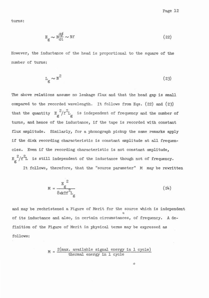
IV. Experimental Results for Inductive Source
An experiment was performed to verify the theoretical prediction that
a maximum signal-to-noise ratio exists for an optimum value of source in-
ductance . Since the source inductance was to be varied, a high input imped-
ance to the transistor amplifier was desired so that the gain function
l G(f)/G(f0
)\ 2
should not change with source inductance. The signal-to-
noise ratio s0
at 1 kc as a function of source inductance L was deg
termined theoretically and experimentally as follows.
A transistor feedback amplifier was constructed with a constant voltage
gain between low and high frequency roll-offs of 12 db per octave, the
break frequencies being approximately 100 cps and 5 kc. The first stage
of the amplifier contained the same t ransistor, at the same operating point,
whose noise characteristics are shown in Figs . 6 and 7. The input impedance
was not less than 2Mn throughout the passband. The resistor R1 was
negligibly large, and R2 was J.kn . Since Rgm = 0 .63kn and Fm = 5.6
( 7. 5 db} , the circuit parameters can be found from Eqs. ( 20} and { 21.) to
be c1 = 1.88, c2 = 1. By use of Eqs. (18) and (19) and straight-line
approximations to the gain characteristic, the gain parameters may be found
analytically to be ~ ~0,082 (cps)-1
/ 2, A2 ~410 (cps)1
/ 2 at f0
= lk.c.
Numerical integration of the measured gain characteristic led to more
-l/2 1/2 accurate values of '\ = 0 .076 (cps) , A
2 = 420 (cps) , and it may
be noted that the approximate analytical values are quite adequate for
practical applications. If an inductive signal source with a Figure of Merit
M = 109 (90 db) at 1 kc is assumed, Eqs. (25) and (26) predict that the
amplifier should exhibit a maximum signal-to-noise ratio SOm = 65.7 db
when the source inductance has an optimum value L = 0.0343 h. gm
Experimental measurements of output signal-to-noise ratio were made on
the amplifier with a true rms voltmeter. The signal source was a simulated

magnetic tape head consisting of a variable inductance
Page 16
L in series with g
a 1 kc voltage Eg from an oscillator whose magnitude was adjusted to
maintain a constant Figure of Merit of 90 db: thus, from Eq. (24),
2 -4 2/ E /L = 1.03 x 10 v h. g g
The results are shown in Fig. 8, in which the
solid curve is the predicted 1 kc signal-to-noise ratio as a function of
source inductance with SOm = 65.7 db and L = 0 • 0 34 3 h. gm
The points are
the measured values obtained with the dummy inductive source. The agreement
between predicted and measured values is quite close.
v. Concl usions
The noise performance of transistor amplifier circuits fed from resis-
tive and reactive sources has been discussed.
For resistive sources, it has been shown that a minimum noise figure
exists for an optimum source resistance, that these quantities are inde-
pendent of any feedback, but dependent on equivalent input shunt r esistance
and on equivalent emitter degeneration resistance in the f i rst stage CE
transistor. The presence of these two resistances increases the minimum
noise figure, but the degradation is only slight with resistance values
easily achieved in practice.
For i nductive sources, such as a magnetic tape head or a magnetic
phonograph pickup, it has been shown that a Figure of Merit can be ascribed
to the source which is independent of its inductance. It has further been
shown that a maximum signal- to-noise ratio is at~nable at the amplifier
output for an optimum source inductance. Expressions for these two quanti-
ties have been given in terms of the source Figure of Merit, first-stage
transistor noise properties, circuit parameters and gain parameters. Typi-
cal figures and experimental results in close agreement with theory have
been presentee..

Page 17
It is to be emphasized that the crit eria for best noise performance,
whether the source is resistive or reactive, are in no ~ay connected with
the criteria for maximum power transfer from the source.
ACKNOWLEOOMENTS
Part of this material is based on work performed for Westrex Corpora
tion, Hollywood, California, and is reported by permission of Westrex
Corporation. The author also wishes to thank A. G. D1 Loreto and T. C.
Sorensen, of the California Institute of Technology, who performed the
experimental measurements, and the Alectra Division of Consolidated Electro
dynamics Corporation, Pasadena, California, for their kind loan of a true
rms voltmeter.
REFERENCE
1. P. M. Bargellini and M. B. Herscher, "Investigations of noise in audio
frequency amplifiers using junction transistors 1 " Proc. IRE., vol. 4 3,
pp . 217-226J February 1955.
• '
•
FIGURE CAPI'IONS
1. Simple equivalent circuit of CE transistor amplifier fed from resistive
source.
2. Noise figure F vs. source resistance R for the amplifier of Fig. 1. g
3. Generalized transistor amplifier fed from reactive source, including
input (base) shunt resistance and emitter degeneration resistance with
thermal noise, also feedback generators which are functions of amplifier
output voltage.
4. Optimum source resistance R gm
of thermal noise generated in
as a function of R1
or R2
• Neglect
~ and R2 introduces only small error.
5. Increase in minimum noise figure caused by ~ or R2
. Neglect of
thermal noise generated in ~ and R2 introduces only small error.
6. Comparison between p~dicted and measured noise figure curves as func
tions of source resistance, for resistive source and R2
= 0. Thermal
noise generated in R1 was neglected in computing the predicted curves.
' 7. Comparison between predicted and measured noise figure curves as func
tions of source resistance, for resistive source and ~=co . · Ther
mal noise generated i~ R2 was neglected in computing the predicted
curves.
8. Comparison between predicted and measured signal-to-noise ratio as
functions of source inductance. Source Figure of Merit taken as
M = 109 (90 db) .
Transistor
F
"r---1 a ie l
8 I
F i ~· 1
•
...!111:: 0 0 .0 "U Q)
~
w
w c
::::> ' +
I I L_
0' w
+ I
I I I I I I I I I I I I I I I J
. a--·-
LL

10 5
-e( e
0
1
01
a::
a::
'- 0 e,-e
01
0
a::
a::
•
Rgm
V
S.
Fm =
3 d
b {I
) R
om' I
Rom
vs
.
Rgm
(R
2 =
0)
R, R2
{R1
=en
) Ro
m
Rgm
= I k
.O.
I (R
na=
0.5
k.O
.) /
I om
(2)
As
(I),
bu
t ne
glec
ting
ther
mal
no
ise
in
11
R1 an
d R
2 {in
depe
nden
t o
f Fm
and
R
0m
) I
I / 'I
//
'/ /
I ,.
(I)
/ I
... /
// (
2l
I ,.,
..""
I .,.,
--
--I
-------
-----~--
1 I I
~ ~
05~--------~--~--------~--~----------------~---
o.or
o.
o5
0.1 R
R
o.5
1
5 10
~or__!..
R1
R0m
Fi
g. 4

,_,---
------
--0~------------------~~------~------------------~~------~
0.1
0.5
I R
R
5
10
__!!!
!_.
or
_3
_.
R1
Rom
Fi
~.5

..0
~ ..
Q) ~
::J
Cl
lL
Q)
(/)
0 z ()
~ -
25
'
10 5
Rg
R,
', ~Locus o
f M
inim
a
' ' '
' '
R1=
0.3
0 k
fi
\
-!
-~---
Fm
=7
.5d
b
I
Rgm
=0.
63 k
il
Cur
ves
= P
red
icte
d
Va
lue
s P
oin
ts
= M
ea
sure
d V
alu
es
QL
_ _
__
__
__
__
_ ~----L-----------~----~
Ql
0.5
I 5
10
Rg
, kfi
Fi
~. 6

.Q
"'0 Q)
(/) ·- 0 z (.)
~
5
R2
=3
k!l
J
R2
= lk
!l
j
Rg
0 /
/
R2
/ /
/
/
---'
-f --~-
--s,
r---
F m =
7. 5
db
I
Cu
rve
s P
oin
ts
I
Rgm
= 0
.63
k!l
=
Pre
dic
ted
V
alue
s =
Mea
sure
d V
alue
s
Lo
cus
of
Min
ima
\///
/
/
/
0 O~.~~--------~Q~5----~~------------~5----~IO
R9
, kf
i Fi
~. 7

65
So db
60
Cur
ves
= P
red
icte
d
Val
ues
Poi
nts
= M
easu
red
Val
ues
. 0
0
M=
90
db
a
t I k
c
Sou
rce
55
----
0.01
L9m
=0.
034
h I I r
---S
om
= 65
.7 d
b
2M!l
L9,h
0 0
0
Am
plif
ier
0.05
Fi~-
8
0 o
o
0.1
Oo
o o
•

TRANSISTOR AC AND 00 AMPLIFIERS WITH HIGH INPUT IMPEDANCE
ABSTRACT
A class of transistor amplifiers is described in
which high input impedance is achieved with good bias
stability. Input impedances of the order of _megohms
shunted by one or two micramicrofarads are easily realized
with simple circuits, and higher impedances may be obtained
with more elaborate circuitry. Other important properties
are that input shunt capacitance can be almost completely
eliminated, the voltage gain is stabilized, and the output
impedance is low. Typical practical measurements are
given, and various illustrative circuits are shown for
both ac and de amplifiers.
Page 1
I. Introduction
The inherently low input impedance of a transistor requires specific
effor ts on the part of the circuit designer to achieve higb input imped-, ances i n transistor amplifiers. Same form of negative feedback will solve
this problem; however, a high degree of bias stability is usually re-
quired, and when faced with a practical design one's fir st conclusion is
that high input impedance and high bias stability are incompatible.
Since the emitter- follower configuration offers the highest input
impedance of the three, attempts have been made to achieve high input
1 impedances by using one or more emitter followers in cascade , as shown
in Fig. 1. The input impedance of such a single emitter- follower stage
is approximately ~R shunted by the parallel combination of the collec-
tor resistance and capacitance . By operating the stage at l ow current,
the i nput impedance may be made high . There are three major disadvantages
of this arrangement: (1) the operating point is completely unstabilized,
since the floating base forces the collector current to be approximately
~Ico' where IcO is the collector saturation current, and hence is ex
ponentially dependent on temperature; (2) the input resistance is shunted
by the collector capacitance; (3) when driven from a high impedance
source, which would often be the case when a high-impedance input is called
for, the frequency response is limited by the ~ cutoff frequency of the
transistor .
Attempts to improve the bias stability must involve setting the volt-
age level of the input base, which in turn requires a low-impedance bias
source such as shown in Fig. 2. Thus immediately the previously high in-
put impedance is shunted by the low impedance bias source, leading to the
incompatibility mentioned above.

Page 2
Many improvements can be made in the basic circuit of Fig. 2 to in-
crease the input impedance and yet maintain adequate bias stability.
Such attempts involve multi-stage amplifiers with ac negative feedback
to stabilize gain, de negative feedback to stabilize operating points,
and ''bootstrapping" the input bias potential divider to minimize its
2 shunting effect on the input impedance . The bootstrapping technique
actually involves positive feedback with less-than-unity loop gain.
All these well-established techniques are applicable to the circuits
to be described in this paper, which utilize in addition both negative
and positive feedback with greater- than-unity loop gain . These circuits
exhibit, even without bootstrapping, input resistances of the order of
megohms with a high degree of bias and gain stability 1 and moreover the
detrimental effects of input- stage collector capacitance and input stray
capacitance can be almost completely eliminated. A typical figure for
the input impedance of such an amplifier is 4Mn shunted by 1~~, mea-
sured at the input end of a shielded cable with 73~~ shunt capacitance.
Examples of both ac and de high impedance ampl\fiers will be given in
the following sections .
II. Principles of the new high- impedance circuit
The basic fonn of the new high input impedance ac amplifier is shown
in Fig. 3. The circuit contains a two-stage common-emitter amplifier,
and bias stability is achieved by the battery- resistor combination Eb' ~' which represents any of the many forms of bias arrangement, such as the
potential divider type shown in Fig . 2.
Consider first the de bias conditions . If ~ is small, the base
current of transistor No . 1 is able to take the value required to make
the voltage drop across R1 equal to ~ . Because of the current gain
Page 3
of transistor No . 2, the current through R2
is almost the same as that
through R1
• Thus the voltage across (R1 + R2), which is the output
de level, is approximately Eb(R1
+ R2)/R
1, and is hence stabilized
against changes in both the ~ and the Ico of both transistors . This
is a well-known solution to the bias stability problem, but has hereto-
fore been inapplicable to high input impedance circuits because the bias
resistor ~ limits the input impedance. However, in the new circuit
this difficulty is overcome by the positive feedback link through Rn
and C , as shown below. n
Consider next the ac signal conditions. A simple ac equivalent cir-
cui t of Fig . 3 may be drawn as shown in Fig. 4. Each transistor is re-
presented by a simple equivalent circuit in which the base and emitter
resistances are neglected and the collector current is ~ times the base
current . The collector impedance of No. 2 is neglected since it is in
parallel with the relat ively small (R1 + R2
) ; however, the collector
impedance of No . 1 (collector resistance r c
in parallel with the space-
charge capacitance C ) is important, and effectively appears between c
the input tenninal A and ground (since the collector of No . 1 is
effectively at ac ground through the base-emitter junction of No. 2) .
Also appearing between A and ground are the bias source resistance ~
and any stray capacitance
elements c ' c
C between the input leads. s
The four parallel
C may all be lumped together in an admittance s
Yi, and the parallel combination of Rn and C may be represented by n
an admittance y • n
The following approximations may be made, where the symbols are as
defined in Fig. 4:
(a) ~2 >> 1, hence the current through R1 is essentially the same
as that through R2 .
Page 4
(b) 1 /Yn >> R1 + R2, hence if << ~1~2~1 and the current through
R2 (and R1 ) is essentially equal to ~1~2ibl' To compute the voltage gain, consider a signal voltage +v1 applied
at the input. Since the base and emitter resistances of No . 1 are neg-
lected, the voltage across ~ is vl. Hence, because of approximation
(a), the output voltage at B is equal to vl(Rl + R2)/Rl . Thus the
voltage gain G is v
v Rl + R2 G 2 (1) = - = v vl Rl
and is greater than 1 and is independent of transistor parameters .
The input impedance is by definition v1/i1 , or the input admittance
yin is
( 2)
By summing currents at junction A:
( 3)
where
(4)
= y (R2 l v (7) n n1
1
Page 5
Hence
(8)
The interpretation of this result is as follows:
(a) The term l/~1~ZRl is the admittance at the input of the first
transistor, and can easily be made many megohms.
(b) The term Yi expresses the shunting effect of transistor col-
lector admittance, bias supply resistance, and stray admittance across
the input. The bias suppl y resistance I), is essential if any attempt
is made to stabilize the de operating condition. By proper bootstrapping
techniques both I), and the collector impedance may be r aised in effec
tive value, but not eliminated . However, this approach can not reduce
the effect of the stray capacitance C , and in general will increase its s
value with detrimental results.
is a result of the feedback network Y n
and acts to reduce the effect of the other two . Clearly, by proper
choice of component values, the input admittance can be made small, zero,
or even negative.
It might seem that the optimum choice of y n
would be that leading
to zero admittance, or infinite impedance . However, in practice this is
undesirable since the adjustment is quite sensitive to changes in ~1~2 .
To overcome this problem it is only necessary to choose y n
such that
the second and third terms exactly cancel. This adjustment is independent
of transistor parameters. For this condition
y n
(9)

Page 6
The input impedance zin is then
(10)
which is the theoretical limit obtainable with conventional circuits
assuming perfect bootstrapping and no stray input admittance. This imped-
ance can easily be made higher than any value nonnally required in prac-
tice.
Under the condition Yn = Yi(R1/R2
) described above, the circuit
exhibits the following properties:
(1) Stabilized de operating conditions determined by the bias supply
~' ~ and independent of transistor parameters. Various bias methods
equivalent to and superior to the bias supply ~' ~ are discussed
later.
independent of transistor parameters.
(3) The input impedance is large, i.e., Zin = 13113A and remains
large up to the 13 cutoff frequency of transistor No . 1 or No. 2. Note
in particular that t he stray admittance across the input tennin8.ls and
the collector admittance of No . l do not shunt Zin: these effects have
been removed in the circuit adjustment .
(4) The output impedance is low, being (R2
/132
) if driven from a
low impedance source .
Practical adjustment of the circuit to a desired input impedance is
conducted as follows. The approximate value of R is given by n
(ll)
Page 7
which is Eq. (9) for low frequencies and in which the shunting effect of
r is neglected. The exact value of R is set by a dynamic measure-c n
ment: observe the output voltage v2
when the input is fed through a
source resistance Rs f rom an oscillator set to same midband frequency,
say lkc . Let the output voltage be when R s is present, and v '
2
when R is short- circuited . The input resistance is then s
R = ,---:-'is......--r-_7
(v2
•/v2
) - 1 (12)
and Rn can be adjusted until Rin reaches the desired value . For
example, if the output voltage is lv with R s
absent, then the input
resistance will be 1Mn if R is adjusted so that the output voltage n
falls to 0. 5v when R = lMn s
is inserted in series with the input.
The value of C is next adjusted so that the output voltage stays n
at the same value up to as high a frequency as possible, measured with
R present and the oscillator output maintained at constant amplitude. s
It will be found that it is possible to increase the output voltage at
higher frequencies in this way; this corresponds to over- compensation of
the total shunt input capacitance (c + c ) . c s
Such a condition is
liable to introduce instability, and c n
should be adjusted so that an
acceptable degree of peaking, perhaps lO'f.,, is achieved.
Measurements made on a typical circuit after adjustments were made
in this way are given in Section III.
III . Practical ac high-impedance amplifier
Many practical embodiments of the basic circuit of Fig. 3 are pos-
sible. The most obvious modification eliminates the separate bias battery
Eb by substitution of a potential divider as shown in Fig. 2: the

' Page 8
effective ac value of ~ is then the parallel combination of the two
bias resistors.
Although the collector current of t ransistor No. 2 may be well
stabilized, as described in the previous section, a disadvantage of the
basic circuit of Fig. 3 is that the collector current of No. 1 is equal
to the base current of No . 2, and is therefore small and may be widely
variable from one circuit to another. A way to overcame this difficulty
is shown in Fig. 5, which also contains same other improvements. The
collector current of No. 1 is determined by the de voltage across R3
and the emitter bias resistor R6, the base voltage of No. 2 is determined
by the drop across R8, and the collector current of No. 2 is then fixed
by Rr. Overall de negative feedback to improve the bias stability still
fUrther is obtained by returning the high end of the bias resistor R5
to the low end of R7
, instead of to the supply voltage. It will be
noted that the ac equivalent circuit of this arrangement is identical
with that of the basic circuit shown in Fig. 4, except that the effective
value of ~ is increased because both bias resistors are
bootstrapped to the emitter of No. 1. It will also be noticed that in
Fig. 6 the blocking condenser in series with R n
and en has been
omitted: this improves the low-frequency performance of the amplifier,
but has the disadvantage that positive feedback exists at de which tends
to degrade t he bias stability.
Practical design values and performance data will be given for a typi-
cal ac high impedance amplifier of the general type discussed in the pre-
vious section. The circuit is shown in Fig. 6, and contains bias arrange-
ments somewhat less elaborate than those shown in Fig . 5. No attempt is
made to bootstrap the bias resi stors; however, de negative feedback is
applied to the bias resistors, and the collector current of No. 1 is f ixed

Page 9
at about 0.25ma by the presence of R8. The collector current of No.
2 i s stabilized at lma, and hence the voltage operating level of the
No. 2 emitter is -lOv, and t hat of the No . 2 collector is - 5v. The
common-emitter current-gains of the two transistors used were ~l = 75,
~2 = 64. The equivalent bias resistor I\, is the value of R3
in
parallel with R4, or 4okn; hence it is expected that the positive feed
back resistor should be (R/R1 )I1, = l6okn. Since fine adjustment of
R is required, the circuit suitably contains a 1 20kn fixed resistor n
in series with a 50kn potentiometer.
The voltage gain of the circuit is (R1 + R2)/~ = 4.9, and was mea
sured to be 5 .0 at lkc. The gain was not noticeably less at 5cps,
and fell by 3db at 1. 3Mc . The magnitude of t he input impedance, ( Zinl ,
is shown in Fig. 7 as a function of fre quency for various conditions.
Curves 1 and 2 show j Zinl as a fUnction of f r equency when Rin at lkc
is adjusted to 4Mn and to lMn, respectively, as described in the pre-
vious section . It is observed that the high impedance is maintained to
over lOOkc in each case, and the decr ease in l zin l at higher frequen
cies may roughly be ascribed to the presence of an effective shunt input
capacitance of 1~-t~. Curve 3 shows } Zin \ as a function of f r equency
when R. at lkc is adjusted to lMn in the presence of an input ~n
shielded cable with 7 3~-t~ shunt capacitance . The equivalent input shunt
capacitance is about 2~-t~: note that this is the apparent capacitance at
the input of the shielded cable .
The decrease in jzin l at low frequencies is caused by the 0.5~ ca-
pacitor C in series with Rn and C . n This was purposely made small
in order to illustrate its effect . At first glance it would appear that
jzin l should be reduced by a factor of 2 at a f requency f 0 = l / 2nRnC;
Page 10
however, analysis shows that this frequency is actually f 0 = Rin/2nRnCRin 1'
R0
present.
and R 1
in are the midband input resistances with and without
Thus the effective time constant R C is reduced Whenever n
positive feedback is introduced to increase the input impedance. Substitu-
tion of numerical values R = 16ok.n, C = 0 . 5~, R 1 = 4ok.n ( ~ R ) n in -o
shows that is about 50 cps for R = lMn in and about 200cps for
Rin = 4Mn. These values are in reasonable agreement with the results of
Fig. 7. The high input impedance can, of course, easily be extended to
lower frequencies by increasing C, or C can be omitted altogether with
consequent degradation in de stability.
Figure 8 shows the output resistance Rout at lkc of the circuit
of Fig . 6, as a function of source resistance R . s The presence of posi-
ti ve feedback to increase Rin also increases R at high values of out
source resistance; obviously if R = O, s
R out is independent of any
positive feedback, and the predicted value is easily seen from Fig. 4 to
be Rout = R4/13 2• The curves shown in Fig. 8 were taken with a transistor
No. 2 having 132 = 34, thus R t = 3900/34 = ll5n Which agrees well ou
with the measured results for R ~0. Although the output resistance s
is not large unless high values of source resistance are used, the output
resistance can, of course, be reduced by addition of an emitter- follower
stage to the output .
It is of interest to observe the effects of changing transistors on
the operating points and on the input impedance. Table I shows the
variations in the output de voltage v0 and in the input resistance Rin
at lkc as transistors were changed. It can be seen that the operating
point is well stabilized, but that re-adjustment of
to maintain Rin constant .
R n
would be necessary

Page ll
TABLE I
t31 t32 vo Rio
75 64 5 .0v l .OMn
52 64 4 . 6 0.8
75 34 5.0 0.6
52 34 4 . 5 0 . 5
It is impractical to try to adjust the input resistance to more than
about 100 times the value of I\' hence in the practical circuit of Fig.
6 4Mn is about the highest input resistance 'Which can be achi eved v.l th
r easonabl e stabi lity. However, if bootstrapping were employed as shown
in Fig. 5, input r esistances higher than 4Mn could easily be achieved.
IV . De high impedance ampl ifiers
The principles outlined in the previous sections may be extended to
de amplifiers by the addition of a third transistor.
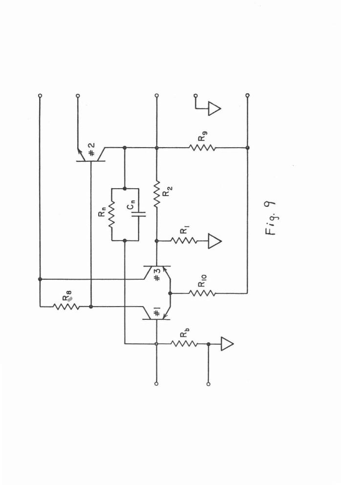
One possible basic arrangement is shown in Fig. 9· By proper choice
of component values, both the input and output may be set at ground level
for zero signal . Both positive- and negative-going signals can-be
accommodated. The voltage gain is (R1 + R2)/R1 , and the input admittance
yin is
where Yi
in Fig. 9.
(13)
and Y are as defined in Fig. 4 and have the same significance 0
Another possible arrangement of a high impedance de amplifier is
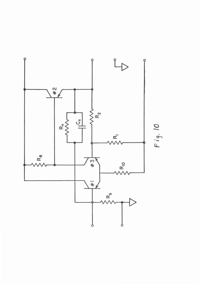
shown in Fig . 10. This circuit differs from that of Fig. 9 in that
transistor No. 2 is in common-collector instead of in common-emitter

Page 12
connection, and to maintain correct phase relationships the base drive
for No. 2 must be derived from the collector of No. 3 instead of from
that of No. 1. The vol ta.ge gain is again (R1 + R2) /R1, and the input
admittance is
(14)
The relative merits of the cir cuits of Figs. 9 and 10 are as follows.
In Fig. 10, the output can not be set at zero de level, unless the out-
put is taken from the junction of ~ and R2
instead of from the
emitter of transistor No. 2, in which case the voltage gain is unity.
The first term on the right-hand side of the equation for the i nput admit-
tance is larger for the circuit of Fig. 10 than for that of Fig. 9, hence
a greater degree of positive feedback through Yn is necessary to attain
a given input admittance. In the circuit of Fig . 10, all the transistors
are of the same type, and also the phase shift within the feedback loop
is less than in the circuit of Fig . 9, and hence greater stability re-
sults.
V. Conclusions
Principles of transistor amplifiers have been described which employ
both negative and positive feedback, whth greater-than-unity loop gain,
to realize high input impedance with good bias stability. Two-stage ac
amplifiers and three-stage de amplifiers are described which exhibit input
impedances of the order of megohms shunted by one or two micromicrofarads.
Ac bootstrapping would enable even higher ac impedances to be realized
with the same degree of bias stability. ~ther desirable features are
that input shunt capacitance, such as that of a shielded cable, can be
Page 13
almost completely eliminated, the voltage gain is greater than unity and
is stabilized, and the output impedance is low for low source impedances.
Typical practical measurements are given, and various illustrative cir
cuits are shown for both a.c and de amplifiers.
The authors wish to thank A. G. DiLoreto, T. C. Sorensen, and W. T.
McDonald, of the California Institute of Technology, for their help with
the experimental measurements. Patents covering many of the circuits
have been applied for by the California Institute of Technology.

REFERENCES
1. A. E. Bachmann, "Transistor low noise preamplifier with high input
impedance," presented at the Transistor and Solid State Circuits
Conference, Philadelphia, February 1957.
2. P . J. Anzalone, "A high input impedance transistor circuit,"
Electronic Design, Vol . 5, June 1 , l957J pp . 38- 41 .

FIGURES
1. Basic emitter-follower circuit for obtaining high input impedance .
2. Bias- stabilized emitter- follower circuit.
3. Basic circuit of a high input impedance, bias- and gain- stabilized
amplifier.
4. Ac equivalent circuit of the high impedance ampli fier of Fig. 3.
5. Possi ble modifications of the basic high impedance ampl ifier, incl ud
ing de negative feedback to increase bias stability, and bootstrapp
ing to increase the input impedance.
6. Practical high impedance amplifier with voltage gain of 5, input
impedance up to 4Mn shunted by lJl~ .
7. Input impedance as a function of frequency for the circuit of Fig. 6.
8. Output resistance as a function of source resistance for the circuit
of Fig. 6.
9. One fonn of high impedance de amplifier. Both input and output can
be set at ground level .
10 . Another fonn of high impedance de amplifier . Output can not be set
at ground level except with unity voltage gain.
R
F ;~. 1

+
c: . 0: 0, -
LL
-
(\J > + m
> +
(\J
a::
ll
a::
ltl
(.)

8
(I)
0::
It)
0:: c
0::
+
·-lL.
8
T

> 10 . C\J
I
~ mo a:: -
c: a::
~
0 0 !'(')
-:1. 10
(.) 0 L----y
T
- ~ a::
. ~ ·-

10~----~~~------~--~------~~------~--~------~~
5 CD
4 M
n at
1 kc
-----..
IZinl
®
1 Mn
at
Ike
IMnl
/
1::::::
1 r
I ~
®
1 Mn
at
Ike -------
with
7
3 p.
.p..
f in
pu
t ca
ble
capa
cita
nce
OJ..
...__ _
_ __
., _
_,__
__
_ _.
____
_, _
__
__
_ -'-
_ __
._ _
__
_.__
_L--
-_--
L--
--L
..__
__.
10
100
Ike
10
100
I Me
FREQ
UEN
CY
Fij
. 7
c: ::E
0 0
0
c: L-----~--~----------~----~---------W~ c:
~
0
3~N'VlSIS3~ lndlnO
~ 0 0
c.J u z <t t-(/) C() (/) w . a: 0"-> ·-w u LL. a:: ::::> 0 (/)
c 0::
N 0::
(7)
0::
·-u..
0 -. Ch ·-
Recommended