A Microchip Technology Company
©2011 Silicon Storage Technology, Inc. DS25028A 08/11
Not Recommended for New Designs
www.microchip.com
16 Mbit / 32 Mbit / (x16) Multi-Purpose Flash PlusSST39VF1601 / SST39VF3201SST39VF1602 / SST39VF3202
Features• Organized as 1M x16: SST39VF1601/1602
2M x16: SST39VF3201/3202
• Single Voltage Read and Write Operations– 2.7-3.6V
• Superior Reliability– Endurance: 100,000 Cycles (Typical)– Greater than 100 years Data Retention
• Low Power Consumption (typical values at 5 MHz)– Active Current: 9 mA (typical)– Standby Current: 3 µA (typical)– Auto Low Power Mode: 3 µA (typical)
• Hardware Block-Protection/WP# Input Pin– Top Block-Protection (top 32 KWord)
for SST39VF1602/3202– Bottom Block-Protection (bottom 32 KWord)
for SST39VF1601/3201
• Sector-Erase Capability– Uniform 2 KWord sectors
• Block-Erase Capability– Uniform 32 KWord blocks
• Chip-Erase Capability
• Erase-Suspend/Erase-Resume Capabilities
• Hardware Reset Pin (RST#)
• Security-ID Feature– SST: 128 bits; User: 128 bits
• Fast Read Access Time:– 70 ns
• Latched Address and Data
• Fast Erase and Word-Program:– Sector-Erase Time: 18 ms (typical)– Block-Erase Time: 18 ms (typical)– Chip-Erase Time: 40 ms (typical)– Word-Program Time: 7 µs (typical)
• Automatic Write Timing– Internal VPP Generation
• End-of-Write Detection– Toggle Bits– Data# Polling
• CMOS I/O Compatibility
• JEDEC Standard– Flash EEPROM Pinouts and command sets
• Packages Available– 48-lead TSOP (12mm x 20mm)– 48-ball TFBGA (6mm x 8mm)
• All devices are RoHS compliant
The SST39VF1601/1602 and SST39VF3201/3202 devices are 1M x16 and 2Mx16, respectively, CMOS Multi-Purpose Flash Plus (MPF+) manufactured withSST's proprietary, high performance CMOS SuperFlash technology. The split-gate cell design and thick-oxide tunneling injector attain better reliability and man-ufacturability compared with alternate approaches. The SST39VF1601/1602/3201/3202 write (Program or Erase) with a 2.7-3.6V power supply. These devicesconforms to JEDEC standard pinouts for x16 memories.
Not recommended for new designs. Please use SST39VF1601Cand SST39VF3201B.

©20
16 Mbit / 32 Mbit Multi-Purpose Flash PlusSST39VF1601 / SST39VF3201SST39VF1602 / SST39VF3202
Not Recommended for New Designs
A Microchip Technology Company
Product DescriptionThe SST39VF160x and SST39VF320x devices are 1M x16 and 2M x16, respectively, CMOS Multi-Purpose Flash Plus (MPF+) manufactured with SST’s proprietary, high performance CMOS Super-Flash technology. The split-gate cell design and thick-oxide tunneling injector attain better reliabilityand manufacturability compared with alternate approaches. The SST39VF160x/320x write (Programor Erase) with a 2.7-3.6V power supply. These devices conform to JEDEC standard pinouts for x16memories.
Featuring high performance Word-Program, the SST39VF160x/320x devices provide a typical Word-Program time of 7 µsec. These devices use Toggle Bit or Data# Polling to indicate the completion ofProgram operation. To protect against inadvertent write, they have on-chip hardware and SoftwareData Protection schemes. Designed, manufactured, and tested for a wide spectrum of applications,these devices are offered with a guaranteed typical endurance of 100,000 cycles. Data retention israted at greater than 100 years.
The SST39VF160x/320x devices are suited for applications that require convenient and economicalupdating of program, configuration, or data memory. For all system applications, they significantlyimprove performance and reliability, while lowering power consumption. They inherently use lessenergy during Erase and Program than alternative flash technologies. The total energy consumed is afunction of the applied voltage, current, and time of application. Since for any given voltage range, theSuperFlash technology uses less current to program and has a shorter erase time, the total energyconsumed during any Erase or Program operation is less than alternative flash technologies. Thesedevices also improve flexibility while lowering the cost for program, data, and configuration storageapplications.
The SuperFlash technology provides fixed Erase and Program times, independent of the number ofErase/Program cycles that have occurred. Therefore the system software or hardware does not haveto be modified or de-rated as is necessary with alternative flash technologies, whose Erase and Pro-gram times increase with accumulated Erase/Program cycles.
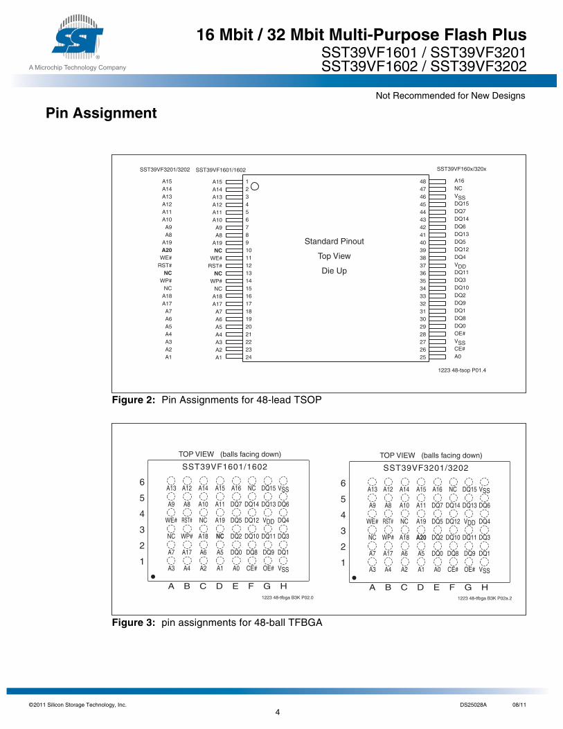
To meet high density, surface mount requirements, the SST39VF160x/320x are offered in 48-leadTSOP and 48-ball TFBGA packages. See Figures 2 and 3 for pin assignments.
11 Silicon Storage Technology, Inc. DS25028A 08/11
2

©20
16 Mbit / 32 Mbit Multi-Purpose Flash PlusSST39VF1601 / SST39VF3201SST39VF1602 / SST39VF3202
Not Recommended for New Designs
A Microchip Technology Company
Block Diagram
Figure 1: Functional Block Diagram
Y-Decoder
I/O Buffers and Data Latches
1223 B1.0
Address Buffer Latches
X-Decoder
DQ15 - DQ0
Memory Address
OE#CE#
WE#
SuperFlashMemory
Control LogicWP#
RESET#
11 Silicon Storage Technology, Inc. DS25028A 08/11
3
©20
16 Mbit / 32 Mbit Multi-Purpose Flash PlusSST39VF1601 / SST39VF3201SST39VF1602 / SST39VF3202
Not Recommended for New Designs
A Microchip Technology Company
Pin Assignment
Figure 2: Pin Assignments for 48-lead TSOP
Figure 3: pin assignments for 48-ball TFBGA
A15A14A13A12A11A10A9A8
A19A20
WE#RST#
NCWP#
NCA18A17A7A6A5A4A3A2A1
123456789101112131415161718192021222324
A16NCVSSDQ15DQ7DQ14DQ6DQ13DQ5DQ12DQ4VDDDQ11DQ3DQ10DQ2DQ9DQ1DQ8DQ0OE#VSSCE#A0
484746454443424140393837363534333231302928272625
1223 48-tsop P01.4
Standard Pinout
Top View
Die Up
SST39VF160x/320x
A15A14A13A12A11A10A9A8
A19NC
WE#RST#
NCWP#
NCA18A17A7A6A5A4A3A2A1
SST39VF1601/1602SST39VF3201/3202
A13
A9
WE#
NC
A7
A3
A12
A8
RST#
WP#
A17
A4
A14
A10
NC
A18
A6
A2
A15
A11
A19
A20
A5
A1
A16
DQ7
DQ5
DQ2
DQ0
A0
NC
DQ14
DQ12
DQ10
DQ8
CE#
DQ15
DQ13
VDD
DQ11
DQ9
OE#
VSS
DQ6
DQ4
DQ3
DQ1
VSS
1223 48-tfbga B3K P02a.2
SST39VF3201/3202
TOP VIEW (balls facing down)
6
5
4
3
2
1
A B C D E F G H
A13
A9
WE#
NC
A7
A3
A12
A8
RST#
WP#
A17
A4
A14
A10
NC
A18
A6
A2
A15
A11
A19
NC
A5
A1
A16
DQ7
DQ5
DQ2
DQ0
A0
NC
DQ14
DQ12
DQ10
DQ8
CE#
DQ15
DQ13
VDD
DQ11
DQ9
OE#
VSS
DQ6
DQ4
DQ3
DQ1
VSS
1223 48-tfbga B3K P02.0
SST39VF1601/1602
TOP VIEW (balls facing down)
6
5
4
3
2
1
A B C D E F G H
11 Silicon Storage Technology, Inc. DS25028A 08/11
4

©20
16 Mbit / 32 Mbit Multi-Purpose Flash PlusSST39VF1601 / SST39VF3201SST39VF1602 / SST39VF3202
Not Recommended for New Designs
A Microchip Technology Company
Table 1: Pin Description
Symbol Pin Name Functions
AMS1-A0 Address Inputs To provide memory addresses.
During Sector-Erase AMS-A11 address lines will select the sector.During Block-Erase AMS-A15 address lines will select the block.
DQ15-DQ0 Data Input/output To output data during Read cycles and receive input data during Write cycles.Data is internally latched during a Write cycle.The outputs are in tri-state when OE# or CE# is high.
WP# Write Protect To protect the top/bottom boot block from Erase/Program operation whengrounded.
RST# Reset To reset and return the device to Read mode.
CE# Chip Enable To activate the device when CE# is low.
OE# Output Enable To gate the data output buffers.
WE# Write Enable To control the Write operations.
VDD Power Supply To provide power supply voltage: 2.7-3.6V
VSS Ground
NC No Connection Unconnected pins.T1.2 25028
1. AMS = Most significant addressAMS = A19 for SST39VF1601/1602, and A20 for SST39VF3201/3202
11 Silicon Storage Technology, Inc. DS25028A 08/11
5

©20
16 Mbit / 32 Mbit Multi-Purpose Flash PlusSST39VF1601 / SST39VF3201SST39VF1602 / SST39VF3202
Not Recommended for New Designs
A Microchip Technology Company
Device OperationCommands are used to initiate the memory operation functions of the device. Commands are writtento the device using standard microprocessor write sequences. A command is written by asserting WE#low while keeping CE# low. The address bus is latched on the falling edge of WE# or CE#, whicheveroccurs last. The data bus is latched on the rising edge of WE# or CE#, whichever occurs first.
The SST39VF160x/320x also have the Auto Low Power mode which puts the device in a nearstandby mode after data has been accessed with a valid Read operation. This reduces the IDD activeread current from typically 9 mA to typically 3 µA. The Auto Low Power mode reduces the typical IDDactive read current to the range of 2 mA/MHz of Read cycle time. The device exits the Auto Low Powermode with any address transition or control signal transition used to initiate another Read cycle, withno access time penalty. Note that the device does not enter Auto-Low Power mode after power-up withCE# held steadily low, until the first address transition or CE# is driven high.
ReadThe Read operation of the SST39VF160x/320x is controlled by CE# and OE#, both have to be low forthe system to obtain data from the outputs. CE# is used for device selection. When CE# is high, thechip is deselected and only standby power is consumed. OE# is the output control and is used to gatedata from the output pins. The data bus is in high impedance state when either CE# or OE# is high.Refer to the Read cycle timing diagram for further details (Figure 4).
Word-Program OperationThe SST39VF160x/320x are programmed on a word-by-word basis. Before programming, the sectorwhere the word exists must be fully erased. The Program operation is accomplished in three steps.The first step is the three-byte load sequence for Software Data Protection. The second step is to loadword address and word data. During the Word-Program operation, the addresses are latched on thefalling edge of either CE# or WE#, whichever occurs last. The data is latched on the rising edge ofeither CE# or WE#, whichever occurs first. The third step is the internal Program operation which is ini-tiated after the rising edge of the fourth WE# or CE#, whichever occurs first. The Program operation,once initiated, will be completed within 10 µs. See Figures 5 and 6 for WE# and CE# controlled Pro-gram operation timing diagrams and Figure 20 for flowcharts. During the Program operation, the onlyvalid reads are Data# Polling and Toggle Bit. During the internal Program operation, the host is free toperform additional tasks. Any commands issued during the internal Program operation are ignored.During the command sequence, WP# should be statically held high or low.
Sector/Block-Erase OperationThe Sector- (or Block-) Erase operation allows the system to erase the device on a sector-by-sector (orblock-by-block) basis. The SST39VF160x/320x offer both Sector-Erase and Block-Erase mode. Thesector architecture is based on uniform sector size of 2 KWord. The Block-Erase mode is based onuniform block size of 32 KWord. The Sector-Erase operation is initiated by executing a six-byte com-mand sequence with Sector-Erase command (30H) and sector address (SA) in the last bus cycle. TheBlock-Erase operation is initiated by executing a six-byte command sequence with Block-Erase com-mand (50H) and block address (BA) in the last bus cycle. The sector or block address is latched on thefalling edge of the sixth WE# pulse, while the command (30H or 50H) is latched on the rising edge ofthe sixth WE# pulse. The internal Erase operation begins after the sixth WE# pulse. The End-of-Eraseoperation can be determined using either Data# Polling or Toggle Bit methods. See Figures 10 and 11
11 Silicon Storage Technology, Inc. DS25028A 08/11
6

©20
16 Mbit / 32 Mbit Multi-Purpose Flash PlusSST39VF1601 / SST39VF3201SST39VF1602 / SST39VF3202
Not Recommended for New Designs
A Microchip Technology Company
for timing waveforms and Figure 24 for the flowchart. Any commands issued during the Sector- orBlock-Erase operation are ignored. When WP# is low, any attempt to Sector- (Block-) Erase the pro-tected block will be ignored. During the command sequence, WP# should be statically held high or low.
Erase-Suspend/Erase-Resume CommandsThe Erase-Suspend operation temporarily suspends a Sector- or Block-Erase operation thus allowingdata to be read from any memory location, or program data into any sector/block that is not suspendedfor an Erase operation. The operation is executed by issuing one byte command sequence with Erase-Suspend command (B0H). The device automatically enters read mode typically within 20 µs after theErase-Suspend command had been issued. Valid data can be read from any sector or block that is notsuspended from an Erase operation. Reading at address location within erase-suspended sectors/blocks will output DQ2 toggling and DQ6 at “1”. While in Erase-Suspend mode, a Word-Program oper-ation is allowed except for the sector or block selected for Erase-Suspend.
To resume Sector-Erase or Block-Erase operation which has been suspended the system must issueErase Resume command. The operation is executed by issuing one byte command sequence withErase Resume command (30H) at any address in the last Byte sequence.
Chip-Erase OperationThe SST39VF160x/320x provide a Chip-Erase operation, which allows the user to erase the entirememory array to the “1” state. This is useful when the entire device must be quickly erased.
The Chip-Erase operation is initiated by executing a six-byte command sequence with Chip-Erasecommand (10H) at address 5555H in the last byte sequence. The Erase operation begins with the ris-ing edge of the sixth WE# or CE#, whichever occurs first. During the Erase operation, the only validread is Toggle Bit or Data# Polling. See Table 6 for the command sequence, Figure 10 for timing dia-gram, and Figure 24 for the flowchart. Any commands issued during the Chip-Erase operation areignored. When WP# is low, any attempt to Chip-Erase will be ignored. During the command sequence,WP# should be statically held high or low.
Write Operation Status DetectionThe SST39VF160x/320x provide two software means to detect the completion of a Write (Program orErase) cycle, in order to optimize the system write cycle time. The software detection includes two sta-tus bits: Data# Polling (DQ7) and Toggle Bit (DQ6). The End-of-Write detection mode is enabled afterthe rising edge of WE#, which initiates the internal Program or Erase operation.
The actual completion of the nonvolatile write is asynchronous with the system; therefore, either aData# Polling or Toggle Bit read may be simultaneous with the completion of the write cycle. If thisoccurs, the system may possibly get an erroneous result, i.e., valid data may appear to conflict witheither DQ7 or DQ6. In order to prevent spurious rejection, if an erroneous result occurs, the softwareroutine should include a loop to read the accessed location an additional two (2) times. If both readsare valid, then the device has completed the Write cycle, otherwise the rejection is valid.
11 Silicon Storage Technology, Inc. DS25028A 08/11
7

©20
16 Mbit / 32 Mbit Multi-Purpose Flash PlusSST39VF1601 / SST39VF3201SST39VF1602 / SST39VF3202
Not Recommended for New Designs
A Microchip Technology Company
Data# Polling (DQ7)When the SST39VF160x/320x are in the internal Program operation, any attempt to read DQ7 will pro-duce the complement of the true data. Once the Program operation is completed, DQ7 will producetrue data. Note that even though DQ7 may have valid data immediately following the completion of an internalWrite operation, the remaining data outputs may still be invalid: valid data on the entire data bus will appear insubsequent successive Read cycles after an interval of 1 µs. During internal Erase operation, any attemptto read DQ7 will produce a ‘0’. Once the internal Erase operation is completed, DQ7 will produce a ‘1’.The Data# Polling is valid after the rising edge of fourth WE# (or CE#) pulse for Program operation. ForSector-, Block- or Chip-Erase, the Data# Polling is valid after the rising edge of sixth WE# (or CE#)pulse. See Figure 7 for Data# Polling timing diagram and Figure 21 for a flowchart.
Toggle Bits (DQ6 and DQ2)During the internal Program or Erase operation, any consecutive attempts to read DQ6 will producealternating “1”s and “0”s, i.e., toggling between 1 and 0. When the internal Program or Erase operationis completed, the DQ6 bit will stop toggling. The device is then ready for the next operation. For Sector-, Block-, or Chip-Erase, the toggle bit (DQ6) is valid after the rising edge of sixth WE# (or CE#) pulse.DQ6 will be set to “1” if a Read operation is attempted on an Erase-Suspended Sector/Block. If Pro-gram operation is initiated in a sector/block not selected in Erase-Suspend mode, DQ6 will toggle.
An additional Toggle Bit is available on DQ2, which can be used in conjunction with DQ6 to checkwhether a particular sector is being actively erased or erase-suspended. Table 2 shows detailed statusbits information. The Toggle Bit (DQ2) is valid after the rising edge of the last WE# (or CE#) pulse ofWrite operation. See Figure 8 for Toggle Bit timing diagram and Figure 21 for a flowchart.
Note: DQ7 and DQ2 require a valid address when reading status information.
Data ProtectionThe SST39VF160x/320x provide both hardware and software features to protect nonvolatile data frominadvertent writes.
Hardware Data ProtectionNoise/Glitch Protection: A WE# or CE# pulse of less than 5 ns will not initiate a write cycle.
VDD Power Up/Down Detection: The Write operation is inhibited when VDD is less than 1.5V.
Write Inhibit Mode: Forcing OE# low, CE# high, or WE# high will inhibit the Write operation. This pre-vents inadvertent writes during power-up or power-down.
Table 2: Write Operation Status
Status DQ7 DQ6 DQ2
Normal Operation Standard Program DQ7# Toggle No Toggle
Standard Erase 0 Toggle Toggle
Erase-Suspend Mode Read from Erase-Suspended Sector/Block 1 1 Toggle
Read from Non- Erase-Suspended Sector/Block Data Data Data
Program DQ7# Toggle N/A
T2.0 25028
11 Silicon Storage Technology, Inc. DS25028A 08/11
8

©20
16 Mbit / 32 Mbit Multi-Purpose Flash PlusSST39VF1601 / SST39VF3201SST39VF1602 / SST39VF3202
Not Recommended for New Designs
A Microchip Technology Company
Hardware Block ProtectionThe SST39VF1602/3202 support top hardware block protection, which protects the top 32 KWordblock of the device. The SST39VF1601/3201 support bottom hardware block protection, which pro-tects the bottom 32 KWord block of the device. The Boot Block address ranges are described in Table3. Program and Erase operations are prevented on the 32 KWord when WP# is low. If WP# is left float-ing, it is internally held high via a pull-up resistor, and the Boot Block is unprotected, enabling Programand Erase operations on that block.
Hardware Reset (RST#)The RST# pin provides a hardware method of resetting the device to read array data. When the RST#pin is held low for at least TRP, any in-progress operation will terminate and return to Read mode. Whenno internal Program/Erase operation is in progress, a minimum period of TRHR is required after RST#is driven high before a valid Read can take place (see Figure 16).
The Erase or Program operation that has been interrupted needs to be reinitiated after the deviceresumes normal operation mode to ensure data integrity.
Software Data Protection (SDP)The SST39VF160x/320x provide the JEDEC approved Software Data Protection scheme for all dataalteration operations, i.e., Program and Erase. Any Program operation requires the inclusion of thethree-byte sequence. The three-byte load sequence is used to initiate the Program operation, provid-ing optimal protection from inadvertent Write operations, e.g., during the system power-up or power-down. Any Erase operation requires the inclusion of six-byte sequence. These devices are shippedwith the Software Data Protection permanently enabled. See Table 6 for the specific software com-mand codes. During SDP command sequence, invalid commands will abort the device to read modewithin TRC. The contents of DQ15-DQ8 can be VIL or VIH, but no other value, during any SDP commandsequence.
Common Flash Memory Interface (CFI)The SST39VF160x/320x also contain the CFI information to describe the characteristics of the device.In order to enter the CFI Query mode, the system must write three-byte sequence, same as product IDentry command with 98H (CFI Query command) to address 5555H in the last byte sequence. Once thedevice enters the CFI Query mode, the system can read CFI data at the addresses given in Tables 7through 10. The system must write the CFI Exit command to return to Read mode from the CFI Querymode.
Table 3: Boot Block Address Ranges
Product Address Range
Bottom Boot Block
SST39VF1601/3201 000000H-007FFFH
Top Boot Block
SST39VF1602 0F8000H-0FFFFFH
SST39VF3202 1F8000H-1FFFFFHT3.0 25028
11 Silicon Storage Technology, Inc. DS25028A 08/11
9

©20
16 Mbit / 32 Mbit Multi-Purpose Flash PlusSST39VF1601 / SST39VF3201SST39VF1602 / SST39VF3202
Not Recommended for New Designs
A Microchip Technology Company
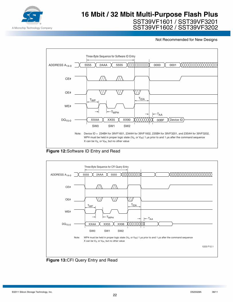
Product IdentificationThe Product Identification mode identifies the devices as the SST39VF1601, SST39VF1602,SST39VF3201, or SST39VF3202, and manufacturer as SST. This mode may be accessed softwareoperations. Users may use the Software Product Identification operation to identify the part (i.e., usingthe device ID) when using multiple manufacturers in the same socket. For details, see Table 6 for soft-ware operation, Figure 12 for the Software ID Entry and Read timing diagram and Figure 22 for theSoftware ID Entry command sequence flowchart.
Product Identification Mode Exit/CFI Mode ExitIn order to return to the standard Read mode, the Software Product Identification mode must be exited.Exit is accomplished by issuing the Software ID Exit command sequence, which returns the device tothe Read mode. This command may also be used to reset the device to the Read mode after any inad-vertent transient condition that apparently causes the device to behave abnormally, e.g., not read cor-rectly. Please note that the Software ID Exit/CFI Exit command is ignored during an internal Programor Erase operation. See Table 6 for software command codes, Figure 14 for timing waveform, and Fig-ures 22 and 23 for flowcharts.
Security IDThe SST39VF160x/320x devices offer a 256-bit Security ID space. The Secure ID space is divided intotwo 128-bit segments - one factory programmed segment and one user programmed segment. Thefirst segment is programmed and locked at SST with a random 128-bit number. The user segment isleft un-programmed for the customer to program as desired.
To program the user segment of the Security ID, the user must use the Security ID Word-Programcommand. To detect end-of-write for the SEC ID, read the toggle bits. Do not use Data# Polling. Oncethis is complete, the Sec ID should be locked using the User Sec ID Program Lock-Out. This disablesany future corruption of this space. Note that regardless of whether or not the Sec ID is locked, neitherSec ID segment can be erased.
The Secure ID space can be queried by executing a three-byte command sequence with Enter Sec IDcommand (88H) at address 5555H in the last byte sequence. To exit this mode, the Exit Sec ID com-mand should be executed. Refer to Table 6 for more details.
Table 4: Product Identification
Address Data
Manufacturer’s ID 0000H BFH
Device ID
SST39VF1601 0001H 234BH
SST39VF1602 0001H 234AH
SST39VF3201 0001H 235BH
SST39VF3202 0001H 235AHT4.2 25028
11 Silicon Storage Technology, Inc. DS25028A 08/11
10
©20
16 Mbit / 32 Mbit Multi-Purpose Flash PlusSST39VF1601 / SST39VF3201SST39VF1602 / SST39VF3202
Not Recommended for New Designs
A Microchip Technology Company
Operations
Table 5: Operation Modes Selection
Mode CE# OE# WE# DQ Address
Read VIL VIL VIH DOUT AIN
Program VIL VIH VIL DIN AIN
Erase VIL VIH VIL X1
1. X can be VIL or VIH, but no other value.
Sector or block address,XXH for Chip-Erase
Standby VIH X X High Z X
Write Inhibit X VIL X High Z/ DOUT X
X X VIH High Z/ DOUT X
Product Identification
Software Mode VIL VIL VIH See Table 6T5.0 25028
Table 6: Software Command Sequence
CommandSequence
1st BusWrite Cycle
2nd BusWrite Cycle
3rd BusWrite Cycle
4th BusWrite Cycle
5th BusWrite Cycle
6th BusWrite Cycle
Addr1
1. Address format A14-A0 (Hex).Addresses A15-A19 can be VIL or VIH, but no other value, for Command sequence for SST39VF1601/1602,Addresses A15-A20 can be VIL or VIH, but no other value, for Command sequence for SST39VF3201/3202,
Data2 Addr1 Data2 Addr1 Data2 Addr1 Data2 Addr1 Data2 Addr1 Data2
Word-Program 5555H AAH 2AAAH 55H 5555H A0H WA3 Data
Sector-Erase 5555H AAH 2AAAH 55H 5555H 80H 5555H
AAH 2AAAH 55H SAX4 30H
Block-Erase 5555H AAH 2AAAH 55H 5555H 80H 5555H
AAH 2AAAH 55H BAX4 50H
Chip-Erase 5555H AAH 2AAAH 55H 5555H 80H 5555H
AAH 2AAAH 55H 5555H
10H
Erase-Suspend XXXXH
B0H
Erase-Resume XXXXH
30H
Query Sec ID5 5555H AAH 2AAAH 55H 5555H 88H
User Security IDWord-Program
5555H AAH 2AAAH 55H 5555H A5H WA6 Data
User Security IDProgram Lock-Out
5555H AAH 2AAAH 55H 5555H 85H XXH6 0000H
Software IDEntry7,8
5555H AAH 2AAAH 55H 5555H 90H
CFI Query Entry 5555H AAH 2AAAH 55H 5555H 98H
Software IDExit9,10/CFI Exit/Sec ID Exit
5555H AAH 2AAAH 55H 5555H F0H
Software IDExit9,10
/CFI Exit/Sec IDExit
XXH F0H
T6.6 25028
11 Silicon Storage Technology, Inc. DS25028A 08/11
11

©20
16 Mbit / 32 Mbit Multi-Purpose Flash PlusSST39VF1601 / SST39VF3201SST39VF1602 / SST39VF3202
Not Recommended for New Designs
A Microchip Technology Company
2. DQ15-DQ8 can be VIL or VIH, but no other value, for Command sequence3. WA = Program Word address4. SAX for Sector-Erase; uses AMS-A11 address lines
BAX, for Block-Erase; uses AMS-A15 address linesAMS = Most significant addressAMS = A19 for SST39VF1601/1602 and A20 for SST39VF3201/3202
5. With AMS-A4 = 0; Sec ID is read with A3-A0,SST ID is read with A3 = 0 (Address range = 000000H to 000007H),User ID is read with A3 = 1 (Address range = 000010H to 000017H).
Lock Status is read with A7-A0 = 0000FFH. Unlocked: DQ3 = 1 / Locked: DQ3 = 0.6. Valid Word-Addresses for Sec ID are from 000000H-000007H and 000010H-000017H.7. The device does not remain in Software Product ID Mode if powered down.8. With AMS-A1 =0; SST Manufacturer ID = 00BFH, is read with A0 = 0,
SST39VF1601 Device ID = 234BH, is read with A0 = 1,SST39VF1602 Device ID = 234AH, is read with A0 = 1,SST39VF3201 Device ID = 235BH, is read with A0 = 1,SST39VF3202 Device ID = 235AH, is read with A0 = 1,
AMS = Most significant addressAMS = A19 for SST39VF1601/1602 and A20 for SST39VF3201/3202
9. Both Software ID Exit operations are equivalent10. If users never lock after programming, Sec ID can be programmed over the previously unprogrammed bits (data=1)
using the Sec ID mode again (the programmed “0” bits cannot be reversed to “1”). Valid Word-Addresses for Sec ID arefrom 000000H-000007H and 000010H-000017H.
Table 7: CFI Query Identification String1 for SST39VF160x/320x
1. Refer to CFI publication 100 for more details.
Address Data Data
10H 0051H Query Unique ASCII string “QRY”
11H 0052H
12H 0059H
13H 0001H Primary OEM command set
14H 0007H
15H 0000H Address for Primary Extended Table
16H 0000H
17H 0000H Alternate OEM command set (00H = none exists)
18H 0000H
19H 0000H Address for Alternate OEM extended Table (00H = none exits)
1AH 0000HT7.1 25028
11 Silicon Storage Technology, Inc. DS25028A 08/11
12
©20
16 Mbit / 32 Mbit Multi-Purpose Flash PlusSST39VF1601 / SST39VF3201SST39VF1602 / SST39VF3202
Not Recommended for New Designs
A Microchip Technology Company
Table 8: System Interface Information for SST39VF160x/320x
Address Data Data
1BH 0027H VDD Min (Program/Erase)DQ7-DQ4: Volts, DQ3-DQ0: 100 millivolts
1CH 0036H VDD Max (Program/Erase)DQ7-DQ4: Volts, DQ3-DQ0: 100 millivolts
1DH 0000H VPP min. (00H = no VPP pin)
1EH 0000H VPP max. (00H = no VPP pin)
1FH 0003H Typical time out for Word-Program 2N µs (23 = 8 µs)
20H 0000H Typical time out for min. size buffer program 2N µs (00H = not supported)
21H 0004H Typical time out for individual Sector/Block-Erase 2N ms (24 = 16 ms)
22H 0005H Typical time out for Chip-Erase 2N ms (25 = 32 ms)
23H 0001H Maximum time out for Word-Program 2N times typical (21 x 23 = 16 µs)
24H 0000H Maximum time out for buffer program 2N times typical
25H 0001H Maximum time out for individual Sector/Block-Erase 2N times typical (21 x 24 = 32ms)
26H 0001H Maximum time out for Chip-Erase 2N times typical (21 x 25 = 64 ms)T8.3 25028
Table 9: Device Geometry Information for SST39VF1601/1602
Address Data Data
27H 0015H Device size = 2N Bytes (15H = 21; 221 = 2 MByte)
28H 0001H Flash Device Interface description; 0001H = x16-only asynchronous interface
29H 0000H
2AH 0000H Maximum number of byte in multi-byte write = 2N (00H = not supported)
2BH 0000H
2CH 0002H Number of Erase Sector/Block sizes supported by device
2DH 00FFH Sector Information (y + 1 = Number of sectors; z x 256B = sector size)
2EH 0001H y = 511 + 1 = 512 sectors (01FF = 511
2FH 0010H
30H 0000H z = 16 x 256 Bytes = 4 KByte/sector (0010H = 16)
31H 001FH Block Information (y + 1 = Number of blocks; z x 256B = block size)
32H 0000H y = 31 + 1 = 32 blocks (001F = 31)
33H 0000H
34H 0001H z = 256 x 256 Bytes = 64 KByte/block (0100H = 256)T9.0 25028
11 Silicon Storage Technology, Inc. DS25028A 08/11
13
©20
16 Mbit / 32 Mbit Multi-Purpose Flash PlusSST39VF1601 / SST39VF3201SST39VF1602 / SST39VF3202
Not Recommended for New Designs
A Microchip Technology Company
Table 10:Device Geometry Information for SST39VF3201/3202
Address Data Data
27H 0016H Device size = 2N Bytes (16H = 22; 222 = 4 MByte)
28H 0001H Flash Device Interface description; 0001H = x16-only asynchronous interface
29H 0000H
2AH 0000H Maximum number of byte in multi-byte write = 2N (00H = not supported)
2BH 0000H
2CH 0002H Number of Erase Sector/Block sizes supported by device
2DH 00FFH Sector Information (y + 1 = Number of sectors; z x 256B = sector size)
2EH 0003H y = 1023 + 1 = 1024 (03FFH = 1023)
2FH 0010H
30H 0000H z = 16 x 256 Bytes = 4 KBytes/sector (0010H = 16)
31H 003FH Block Information (y + 1 = Number of blocks; z x 256B = block size)
32H 0000H y = 63 + 1 = 64 blocks (003FH = 63)
33H 0000H
34H 0001H z = 256 x 256 Bytes = 64 KBytes/block (0100H = 256)T10.2 25028
11 Silicon Storage Technology, Inc. DS25028A 08/11
14

©20
16 Mbit / 32 Mbit Multi-Purpose Flash PlusSST39VF1601 / SST39VF3201SST39VF1602 / SST39VF3202
Not Recommended for New Designs
A Microchip Technology Company
Absolute Maximum Stress Ratings (Applied conditions greater than those listed under “AbsoluteMaximum Stress Ratings” may cause permanent damage to the device. This is a stress rating only andfunctional operation of the device at these conditions or conditions greater than those defined in theoperational sections of this data sheet is not implied. Exposure to absolute maximum stress rating con-ditions may affect device reliability.)
Temperature Under Bias . . . . . . . . . . . . . . . . . . . . . . . . . . . . . . . . . . . . . . . . . . . . . -55°C to +125°CStorage Temperature . . . . . . . . . . . . . . . . . . . . . . . . . . . . . . . . . . . . . . . . . . . . . . . . -65°C to +150°CD. C. Voltage on Any Pin to Ground Potential . . . . . . . . . . . . . . . . . . . . . . . . . . . . -0.5V to VDD+0.5VTransient Voltage (<20 ns) on Any Pin to Ground Potential . . . . . . . . . . . . . . . . . . -2.0V to VDD+2.0VVoltage on A9 Pin to Ground Potential . . . . . . . . . . . . . . . . . . . . . . . . . . . . . . . . . . . . . -0.5V to 13.2VPackage Power Dissipation Capability (TA = 25°C) . . . . . . . . . . . . . . . . . . . . . . . . . . . . . . . . . . 1.0WSurface Mount Solder Reflow Temperature1 . . . . . . . . . . . . . . . . . . . . . . . . . . . 260°C for 10 seconds
1. Excluding certain with-Pb 32-PLCC units, all packages are 260°C capable in both non-Pb and with-Pb solder versions.Certain with-Pb 32-PLCC package types are capable of 240°C for 10 seconds; please consult the factory for the latestinformation.
Output Short Circuit Current2 . . . . . . . . . . . . . . . . . . . . . . . . . . . . . . . . . . . . . . . . . . . . . . . . . . 50 mA
2. Outputs shorted for no more than one second. No more than one output shorted at a time.
Table 11:Operating Range
Range Ambient Temp VDD
Commercial 0°C to +70°C 2.7-3.6V
Industrial -40°C to +85°C 2.7-3.6VT11.1 25028
Table 12:AC Conditions of Test1
1. See Figures 18 and 19
Input Rise/Fall Time Output Load
5ns CL = 30 pFT12.1 25028
11 Silicon Storage Technology, Inc. DS25028A 08/11
15

©20
16 Mbit / 32 Mbit Multi-Purpose Flash PlusSST39VF1601 / SST39VF3201SST39VF1602 / SST39VF3202
Not Recommended for New Designs
A Microchip Technology Company
Table 13:DC Operating Characteristics VDD = 2.7-3.6V1
Symbol Parameter
Limits
Test ConditionsMin Max Units
IDD Power Supply Current Address input=VILT/VIHT2, at f=5 MHz,
VDD=VDD Max
Read3 18 mA CE#=VIL, OE#=WE#=VIH, all I/Os open
Program and Erase 35 mA CE#=WE#=VIL, OE#=VIH
ISB Standby VDD Current 20 µA CE#=VIHC, VDD=VDD Max
IALP Auto Low Power 20 µA CE#=VILC, VDD=VDD MaxAll inputs=VSS or VDD, WE#=VIHC
ILI Input Leakage Current 1 µA VIN=GND to VDD, VDD=VDD Max
ILIW Input Leakage Currenton WP# pin and RST#
10 µA WP#=GND to VDD or RST#=GND toVDD
ILO Output Leakage Current 10 µA VOUT=GND to VDD, VDD=VDD Max
VIL Input Low Voltage 0.8 V VDD=VDD Min
VILC Input Low Voltage (CMOS) 0.3 V VDD=VDD Max
VIH Input High Voltage 0.7VDD V VDD=VDD Max
VIHC Input High Voltage (CMOS) VDD-0.3 V VDD=VDD Max
VOL Output Low Voltage 0.2 V IOL=100 µA, VDD=VDD Min
VOH Output High Voltage VDD-0.2 V IOH=-100 µA, VDD=VDD MinT13.8 25028
1. Typical conditions for the Active Current shown on the front page of the data sheet are average values at 25°C(room temperature), and VDD = 3V. Not 100% tested.
2. See Figure 183. The IDD current listed is typically less than 2mA/MHz, with OE# at VIH. Typical VDD is 3V.
Table 14:Recommended System Power-up Timings
Symbol Parameter Minimum Units
TPU-READ1
1. This parameter is measured only for initial qualification and after a design or process change that could affect this parameter.
Power-up to Read Operation 100 µs
TPU-WRITE1 Power-up to Program/Erase Operation 100 µs
T14.0 25028
Table 15:Capacitance (TA = 25°C, f=1 MHz, other pins open)
Parameter Description Test Condition Maximum
CI/O1
1. This parameter is measured only for initial qualification and after a design or process change that could affect this parameter.
I/O Pin Capacitance VI/O = 0V 12 pF
CIN1 Input Capacitance VIN = 0V 6 pF
T15.0 25028
Table 16:Reliability Characteristics
Symbol Parameter Minimum Specification Units Test Method
NEND1,2
1. This parameter is measured only for initial qualification and after a design or process change that could affect this parameter.2. NEND endurance rating is qualified as a 10,000 cycle minimum for the whole device. A sector- or block-level rating would
result in a higher minimum specification.
Endurance 10,000 Cycles JEDEC Standard A117
TDR1 Data Retention 100 Years JEDEC Standard A103
ILTH1 Latch Up 100 + IDD mA JEDEC Standard 78
T16.2 25028
11 Silicon Storage Technology, Inc. DS25028A 08/11
16

©20
16 Mbit / 32 Mbit Multi-Purpose Flash PlusSST39VF1601 / SST39VF3201SST39VF1602 / SST39VF3202
Not Recommended for New Designs
A Microchip Technology Company
AC Characteristics
Table 17:Read Cycle Timing Parameters VDD = 2.7-3.6V
Symbol Parameter Min Max Units
TRC Read Cycle Time 70 ns
TCE Chip Enable Access Time 70 ns
TAA Address Access Time 70 ns
TOE Output Enable Access Time 35 ns
TCLZ1
1. This parameter is measured only for initial qualification and after a design or process change that could affect thisparameter.
CE# Low to Active Output 0 ns
TOLZ1 OE# Low to Active Output 0 ns
TCHZ1 CE# High to High-Z Output 20 ns
TOHZ1 OE# High to High-Z Output 20 ns
TOH1 Output Hold from Address Change 0 ns
TRP1 RST# Pulse Width 500 ns
TRHR1 RST# High before Read 50 ns
TRY1,2
2. This parameter applies to Sector-Erase, Block-Erase and Program operations.This parameter does not apply to Chip-Erase operations.
RST# Pin Low to Read Mode 20 µsT17.3 25028
Table 18:Program/Erase Cycle Timing Parameters
Symbol Parameter Min Max Units
TBP Word-Program Time 10 µs
TAS Address Setup Time 0 ns
TAH Address Hold Time 30 ns
TCS WE# and CE# Setup Time 0 ns
TCH WE# and CE# Hold Time 0 ns
TOES OE# High Setup Time 0 ns
TOEH OE# High Hold Time 10 ns
TCP CE# Pulse Width 40 ns
TWP WE# Pulse Width 40 ns
TWPH1
1. This parameter is measured only for initial qualification and after a design or process change that could affect thisparameter.
WE# Pulse Width High 30 ns
TCPH1 CE# Pulse Width High 30 ns
TDS Data Setup Time 30 ns
TDH1 Data Hold Time 0 ns
TIDA1 Software ID Access and Exit Time 150 ns
TSE Sector-Erase 25 ms
TBE Block-Erase 25 ms
TSCE Chip-Erase 50 msT18.1 25028
11 Silicon Storage Technology, Inc. DS25028A 08/11
17

©20
16 Mbit / 32 Mbit Multi-Purpose Flash PlusSST39VF1601 / SST39VF3201SST39VF1602 / SST39VF3202
Not Recommended for New Designs
A Microchip Technology Company
Figure 4: Read Cycle Timing Diagram
Figure 5: WE# Controlled Program Cycle Timing Diagram
1223 F03.3
ADDRESS AMS-0
DQ15-0
WE#
OE#
CE#
TCE
TRC TAA
TOE
TOLZVIH
HIGH-Z
TCLZ TOH
TCHZ
HIGH-ZDATA VALIDDATA VALID
TOHZ
Note: AMS = Most significant addressAMS = A19 for SST39VF1601/1602 and A20 for SST39VF3201/3202
1223 F04.4
ADDRESS AMS-0
DQ15-0
TDH
TWPH TDS
TWP
TAH
TAS
TCH
TCS
CE#
SW0 SW1 SW2
5555 2AAA 5555 ADDR
XXAA XX55 XXA0 DATA
INTERNAL PROGRAM OPERATION STARTS
WORD(ADDR/DATA)
OE#
WE#
TBP
Note: AMS = Most significant addressAMS = A19 for SST39VF1601/1602 and A20 for SST39VF3201/3202WP# must be held in proper logic state (VIL or VIH) 1 µs prior to and 1 µs after the command sequenceX can be VIL or VIH, but no other value
11 Silicon Storage Technology, Inc. DS25028A 08/11
18

©20
16 Mbit / 32 Mbit Multi-Purpose Flash PlusSST39VF1601 / SST39VF3201SST39VF1602 / SST39VF3202
Not Recommended for New Designs
A Microchip Technology Company
Figure 6: CE# Controlled Program Cycle Timing Diagram
Figure 7: Data# Polling Timing Diagram
1223 F05.4
ADDRESS AMS-0
DQ15-0
TDH
TCPH TDS
TCP
TAH
TAS
TCH
TCS
WE#
SW0 SW1 SW2
5555 2AAA 5555 ADDR
XXAA XX55 XXA0 DATA
INTERNAL PROGRAM OPERATION STARTS
WORD(ADDR/DATA)
OE#
CE#
TBP
Note: AMS = Most significant addressAMS = A19 for SST39VF1601/1602 and A20 for SST39VF3201/3202WP# must be held in proper logic state (VIL or VIH) 1 µs prior to and 1 µs after the command sequenceX can be VIL or VIH, but no other value
1223 F06.3
ADDRESS AMS-0
DQ7 DATA DATA# DATA# DATA
WE#
OE#
CE#
TOEH
TOE
TCE
TOES
Note: AMS = Most significant addressAMS = A19 for SST39VF1601/1602 and A20 for SST39VF3201/3202
11 Silicon Storage Technology, Inc. DS25028A 08/11
19

©20
16 Mbit / 32 Mbit Multi-Purpose Flash PlusSST39VF1601 / SST39VF3201SST39VF1602 / SST39VF3202
Not Recommended for New Designs
A Microchip Technology Company
Figure 8: Toggle Bits Timing Diagram
Figure 9: WE# Controlled Chip-Erase Timing Diagram
1223 F07.4
ADDRESS AMS-0
DQ6 and DQ2
WE#
OE#
CE#
TOE
TOEH
TCE
TOES
TWO READ CYCLESWITH SAME OUTPUTS
Note: AMS = Most significant addressAMS = A19 for SST39VF1601/1602 and A20 for SST39VF3201/3202
1223 F08.5
ADDRESS AMS-0
DQ15-0
WE#
SW0 SW1 SW2 SW3 SW4 SW5
5555 2AAA 2AAA5555 5555
XX55 XX10XX55XXAA XX80 XXAA
5555
OE#
CE#
SIX-BYTE CODE FOR CHIP-ERASE TSCE
TWP
Note: This device also supports CE# controlled Chip-Erase operation. The WE# and CE# signals areinterchageable as long as minimum timings are met. (See Table 17)AMS = Most significant addressAMS = A19 for SST39VF1601/1602 and A20 for SST39VF3201/3202WP# must be held in proper logic state (VIH) 1 µs prior to and 1 µs after the command sequenceX can be VIL or VIH, but no other value
11 Silicon Storage Technology, Inc. DS25028A 08/11
20

©20
16 Mbit / 32 Mbit Multi-Purpose Flash PlusSST39VF1601 / SST39VF3201SST39VF1602 / SST39VF3202
Not Recommended for New Designs
A Microchip Technology Company
Figure 10:WE# Controlled Block-Erase Timing Diagram
Figure 11:WE# Controlled Sector-Erase Timing Diagram
1223 F09.5
ADDRESS AMS-0
DQ15-0
WE#
SW0 SW1 SW2 SW3 SW4 SW5
5555 2AAA 2AAA5555 5555
XX55 XX50XX55XXAA XX80 XXAA
BAX
OE#
CE#
SIX-BYTE CODE FOR BLOCK-ERASE TBE
TWP
Note: This device also supports CE# controlled Block-Erase operation. The WE# and CE# signals areinterchageable as long as minimum timings are met. (See Table 17)BAX = Block AddressAMS = Most significant addressAMS = A19 for SST39VF1601/1602 and A20 for SST39VF3201/3202WP# must be held in proper logic state (VIL or VIH) 1 µs prior to and 1 µs after the command sequenceX can be VIL or VIH, but no other value
1223 F10.5
ADDRESS AMS-0
DQ15-0
WE#
SW0 SW1 SW2 SW3 SW4 SW5
5555 2AAA 2AAA5555 5555
XX55 XX30XX55XXAA XX80 XXAA
SAX
OE#
CE#
SIX-BYTE CODE FOR SECTOR-ERASE TSE
TWP
Note: This device also supports CE# controlled Sector-Erase operation. The WE# and CE# signals areinterchageable as long as minimum timings are met. (See Table 17)SAX = Sector AddressAMS = Most significant addressAMS = A19 for SST39VF1601/1602 and A20 for SST39VF3201/3202WP# must be held in proper logic state (VIL or VIH) 1 µs prior to and 1 µs after the command sequenceX can be VIL or VIH, but no other value
11 Silicon Storage Technology, Inc. DS25028A 08/11
21
©20
16 Mbit / 32 Mbit Multi-Purpose Flash PlusSST39VF1601 / SST39VF3201SST39VF1602 / SST39VF3202
Not Recommended for New Designs
A Microchip Technology Company
Figure 12:Software ID Entry and Read
Figure 13:CFI Query Entry and Read
1
ADDRESS A14-0
TIDA
DQ15-0
WE#
SW0 SW1 SW2
5555 2AAA 5555 0000 0001
OE#
CE#
Three-Byte Sequence for Software ID Entry
TWP
TWPH TAA
00BF Device IDXX55XXAA XX90
Note: Device ID = 234BH for 39VF1601, 234AH for 39VF1602, 235BH for 39VF3201, and 235AH for 39VF3202,WP# must be held in proper logic state (VIL or VIH) 1 µs prior to and 1 µs after the command sequenceX can be VIL or VIH, but no other value
1223 F12.1
ADDRESS A14-0
TIDA
DQ15-0
WE#
SW0 SW1 SW2
5555 2AAA 5555
OE#
CE#
Three-Byte Sequence for CFI Query Entry
TWP
TWPH TAA
XX55XXAA XX98
Note: WP# must be held in proper logic state (VIL or VIH) 1 µs prior to and 1 µs after the command sequenceX can be VIL or VIH, but no other value
11 Silicon Storage Technology, Inc. DS25028A 08/11
22

©20
16 Mbit / 32 Mbit Multi-Purpose Flash PlusSST39VF1601 / SST39VF3201SST39VF1602 / SST39VF3202
Not Recommended for New Designs
A Microchip Technology Company
Figure 14:Software ID Exit/CFI Exit
Figure 15:Sec ID Entry
1223 F13.0
ADDRESS A14-0
DQ15-0
TIDA
TWP
TWHP
WE#
SW0 SW1 SW2
5555 2AAA 5555
THREE-BYTE SEQUENCE FORSOFTWARE ID EXIT AND RESET
OE#
CE#
XXAA XX55 XXF0
Note: WP# must be held in proper logic state (VIL or VIH) 1 µs prior to and 1 µs after the command sequenceX can be VIL or VIH, but no other value
1223 F20.2
ADDRESS AMS-0
TIDA
DQ15-0
WE#
SW0 SW1 SW2
5555 2AAA 5555
OE#
CE#
THREE-BYTE SEQUENCE FORCFI QUERY ENTRY
TWP
TWPH TAA
XX55XXAA XX88
Note: AMS = Most significant addressAMS = A19 for SST39VF1601/1602 and A20 for SST39VF3201/3202WP# must be held in proper logic state (VIL or VIH) 1 µs prior to and 1 µs after the command sequenceX can be VIL or VIH, but no other value.
11 Silicon Storage Technology, Inc. DS25028A 08/11
23

©20
16 Mbit / 32 Mbit Multi-Purpose Flash PlusSST39VF1601 / SST39VF3201SST39VF1602 / SST39VF3202
Not Recommended for New Designs
A Microchip Technology Company
Figure 16:RST# Timing Diagram (When no internal operation is in progress)
Figure 17:RST# Timing Diagram (During Program or Erase operation)
Figure 18:AC Input/Output Reference Waveforms
Figure 19:A Test Load Example
1223 F22.1
RST#
CE#/OE#
TRP
TRHR
1223 F23.0
RST#
CE#/OE#
TRP
TRY
End-of-Write Detection
(Toggle-Bit)
1223 F14.0
REFERENCE POINTS OUTPUTINPUT VIT
VIHT
VILT
VOT
AC test inputs are driven at VIHT (0.9 VDD) for a logic “1” and VILT (0.1 VDD) for alogic “0”. Measurement reference points for inputs and outputs are VIT (0.5 VDD) and VOT (0.5VDD). Input rise and fall times (10% 90%) are <5 ns.
Note: VIT - VINPUT TestVOT - VOUTPUT TestVIHT - VINPUT HIGH TestVILT - VINPUT LOW Test
1223 F15.0
TO TESTER
TO DUT
CL
11 Silicon Storage Technology, Inc. DS25028A 08/11
24

©20
16 Mbit / 32 Mbit Multi-Purpose Flash PlusSST39VF1601 / SST39VF3201SST39VF1602 / SST39VF3202
Not Recommended for New Designs
A Microchip Technology Company
Figure 20:Word-Program Algorithm
1223 F16.0
Start
Load data: XXAAHAddress: 5555H
Load data: XX55HAddress: 2AAAH
Load data: XXA0HAddress: 5555H
Load WordAddress/Word
Data
Wait for end ofProgram (TBP,Data# Polling
bit, or Toggle bitoperation)
ProgramCompleted
X can be VIL or VIH, but no other value
11 Silicon Storage Technology, Inc. DS25028A 08/11
25

©20
16 Mbit / 32 Mbit Multi-Purpose Flash PlusSST39VF1601 / SST39VF3201SST39VF1602 / SST39VF3202
Not Recommended for New Designs
A Microchip Technology Company
Figure 21:Wait Options
1223 F17.0
Wait TBP,TSCE, TSE
or TBE
Program/EraseInitiated
Internal Timer Toggle Bit
Yes
Yes
No
No
Program/EraseCompleted
Does DQ6match
Read sameword
Data# Polling
Program/EraseCompleted
Program/EraseCompleted
Read word
Is DQ7 =true data
Read DQ7
Program/EraseInitiated
Program/EraseInitiated
11 Silicon Storage Technology, Inc. DS25028A 08/11
26
©20
16 Mbit / 32 Mbit Multi-Purpose Flash PlusSST39VF1601 / SST39VF3201SST39VF1602 / SST39VF3202
Not Recommended for New Designs
A Microchip Technology Company
Figure 22:Software ID/CFI Entry Command Flowcharts
1223 F21.0
Load data: XXAAHAddress: 5555H
Software Product ID EntryCommand Sequence
Load data: XX55HAddress: 2AAAH
Load data: XX90HAddress: 5555H
Wait TIDA
Read Software ID
Load data: XXAAHAddress: 5555H
CFI Query EntryCommand Sequence
Load data: XX55HAddress: 2AAAH
Load data: XX98HAddress: 5555H
Wait TIDA
Read CFI data
Load data: XXAAHAddress: 5555H
Sec ID Query EntryCommand Sequence
Load data: XX55HAddress: 2AAAH
Load data: XX88HAddress: 5555H
Wait TIDA
Read Sec ID
X can be VIL or VIH, but no other value
11 Silicon Storage Technology, Inc. DS25028A 08/11
27

©20
16 Mbit / 32 Mbit Multi-Purpose Flash PlusSST39VF1601 / SST39VF3201SST39VF1602 / SST39VF3202
Not Recommended for New Designs
A Microchip Technology Company
Figure 23:Software ID/CFI Exit Command Flowcharts
1223 F18.1
Load data: XXAAHAddress: 5555H
Software ID Exit/CFI Exit/Sec ID ExitCommand Sequence
Load data: XX55HAddress: 2AAAH
Load data: XXF0HAddress: 5555H
Load data: XXF0HAddress: XXH
Return to normaloperation
Wait TIDA
Wait TIDA
Return to normaloperation
X can be VIL or VIH, but no other value
11 Silicon Storage Technology, Inc. DS25028A 08/11
28

©20
16 Mbit / 32 Mbit Multi-Purpose Flash PlusSST39VF1601 / SST39VF3201SST39VF1602 / SST39VF3202
Not Recommended for New Designs
A Microchip Technology Company
Figure 24:Erase Command Sequence
1223 F19.0
Load data: XXAAHAddress: 5555H
Chip-EraseCommand Sequence
Load data: XX55HAddress: 2AAAH
Load data: XX80HAddress: 5555H
Load data: XX55HAddress: 2AAAH
Load data: XX10HAddress: 5555H
Load data: XXAAHAddress: 5555H
Wait TSCE
Chip erasedto FFFFH
Load data: XXAAHAddress: 5555H
Sector-EraseCommand Sequence
Load data: XX55HAddress: 2AAAH
Load data: XX80HAddress: 5555H
Load data: XX55HAddress: 2AAAH
Load data: XX30HAddress: SAX
Load data: XXAAHAddress: 5555H
Wait TSE
Sector erasedto FFFFH
Load data: XXAAHAddress: 5555H
Block-EraseCommand Sequence
Load data: XX55HAddress: 2AAAH
Load data: XX80HAddress: 5555H
Load data: XX55HAddress: 2AAAH
Load data: XX50HAddress: BAX
Load data: XXAAHAddress: 5555H
Wait TBE
Block erasedto FFFFH
X can be VIL or VIH, but no other value
11 Silicon Storage Technology, Inc. DS25028A 08/11
29

©20
16 Mbit / 32 Mbit Multi-Purpose Flash PlusSST39VF1601 / SST39VF3201SST39VF1602 / SST39VF3202
Not Recommended for New Designs
A Microchip Technology Company
Product Ordering Information
SST 39 VF 1601 - 70 - 4C - EKE
XX XX XXXX - XX - XX - XXX
Environmental AttributeE1 = non-Pb
Package ModifierK = 48 balls or leads
Package TypeE = TSOP (type1, die up, 12mm x 20mm)B3 = TFBGA (6mm x 8mm, 0.8mm pitch)
Temperature RangeC = Commercial = 0°C to +70°CI = Industrial = -40°C to +85°C
Minimum Endurance4 = 10,000 cycles
Read Access Speed70 = 70 ns
Hardware Block Protection1 = Bottom Boot-Block2 = Top Boot-Block
Device Density160 = 16 Mbit320 = 32 Mbit
VoltageV = 2.7-3.6V
Product Series39 = Multi-Purpose Flash
1. Environmental suffix “E” denotes non-Pb solder.SST non-Pb solder devices are “RoHS Compliant”.
11 Silicon Storage Technology, Inc. DS25028A 08/11
30
©20
16 Mbit / 32 Mbit Multi-Purpose Flash PlusSST39VF1601 / SST39VF3201SST39VF1602 / SST39VF3202
Not Recommended for New Designs
A Microchip Technology Company
Valid Combinations for SST39VF1601SST39VF1601-70-4C-EKE SST39VF1601-70-4C-B3KESST39VF1601-90-4C-EKE SST39VF1601-90-4C-B3KE
SST39VF1601-70-4I-EKE SST39VF1601-70-4I-B3KESST39VF1601-90-4I-EKE SST39VF1601-90-4I-B3KE
Valid Combinations for SST39VF1602SST39VF1602-70-4C-EKE SST39VF1602-70-4C-B3KESST39VF1602-90-4C-EKE SST39VF1602-90-4C-B3KE
SST39VF1602-70-4I-EKE SST39VF1602-70-4I-B3KESST39VF1602-90-4I-EKE SST39VF1602-90-4I-B3KE
Valid Combinations for SST39VF3201SST39VF3201-70-4C-EKE SST39VF3201-70-4C-B3KESST39VF3201-90-4C-EKE SST39VF3201-90-4C-B3KE
SST39VF3201-70-4I-EKE SST39VF3201-70-4I-B3KESST39VF3201-90-4I-EKE SST39VF3201-90-4I-B3KE
Valid Combinations for SST39VF3202SST39VF3202-70-4C-EKE SST39VF3202-70-4C-B3KESST39VF3202-90-4C-EKE SST39VF3202-90-4C-B3KE
SST39VF3202-70-4I-EKE SST39VF3202-70-4I-B3KESST39VF3202-90-4I-EKE SST39VF3202-90-4I-B3KE
Note:Valid combinations are those products in mass production or will be in mass production. Consult your SSTsales representative to confirm availability of valid combinations and to determine availability of new combi-nations.
11 Silicon Storage Technology, Inc. DS25028A 08/11
31

©20
16 Mbit / 32 Mbit Multi-Purpose Flash PlusSST39VF1601 / SST39VF3201SST39VF1602 / SST39VF3202
Not Recommended for New Designs
A Microchip Technology Company
Packaging Diagrams
Figure 25:48-lead Thin Small Outline Package (TSOP) 12mm x 20mmSST Package Code: EK
1.050.95
0.700.50
18.5018.30
20.2019.80
0.700.50
12.2011.80
0.270.17
0.150.05
48-tsop-EK-8
Note: 1. Complies with JEDEC publication 95 MO-142 DD dimensions,although some dimensions may be more stringent.
2. All linear dimensions are in millimeters (max/min).3. Coplanarity: 0.1 mm4. Maximum allowable mold flash is 0.15 mm at the package ends, and 0.25 mm between leads.
1.20max.
1mm
0°- 5°
DETAIL
Pin # 1 Identifier
0.50BSC
11 Silicon Storage Technology, Inc. DS25028A 08/11
32
©20
16 Mbit / 32 Mbit Multi-Purpose Flash PlusSST39VF1601 / SST39VF3201SST39VF1602 / SST39VF3202
Not Recommended for New Designs
A Microchip Technology Company
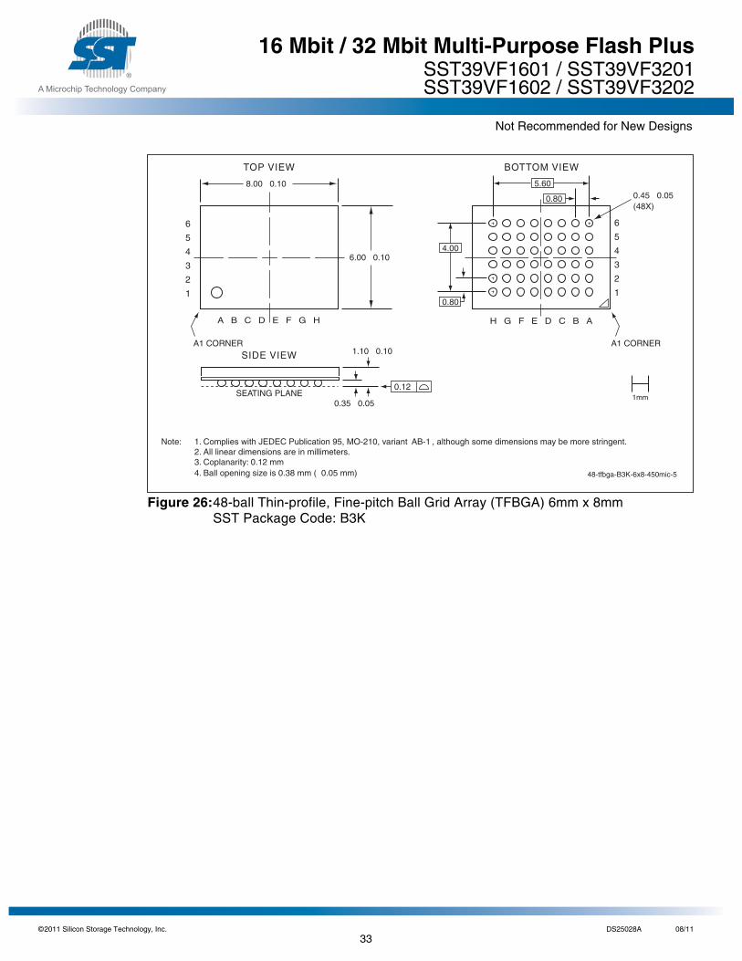
Figure 26:48-ball Thin-profile, Fine-pitch Ball Grid Array (TFBGA) 6mm x 8mmSST Package Code: B3K
A1 CORNER
H G F E D C B AA B C D E F G H
BOTTOM VIEWTOP VIEW
SIDE VIEW
6
5
4
3
2
1
6
5
4
3
2
1
SEATING PLANE0.35 0.05
1.10 0.10
0.12
6.00 0.10
0.45 0.05(48X)
A1 CORNER
8.00 0.10
0.80
4.00
0.80
5.60
48-tfbga-B3K-6x8-450mic-5
Note: 1. Complies with JEDEC Publication 95, MO-210, variant AB-1 , although some dimensions may be more stringent.2. All linear dimensions are in millimeters.3. Coplanarity: 0.12 mm4. Ball opening size is 0.38 mm ( 0.05 mm)
1mm
11 Silicon Storage Technology, Inc. DS25028A 08/11
33
©20
16 Mbit / 32 Mbit Multi-Purpose Flash PlusSST39VF1601 / SST39VF3201SST39VF1602 / SST39VF3202
Not Recommended for New Designs
A Microchip Technology Company
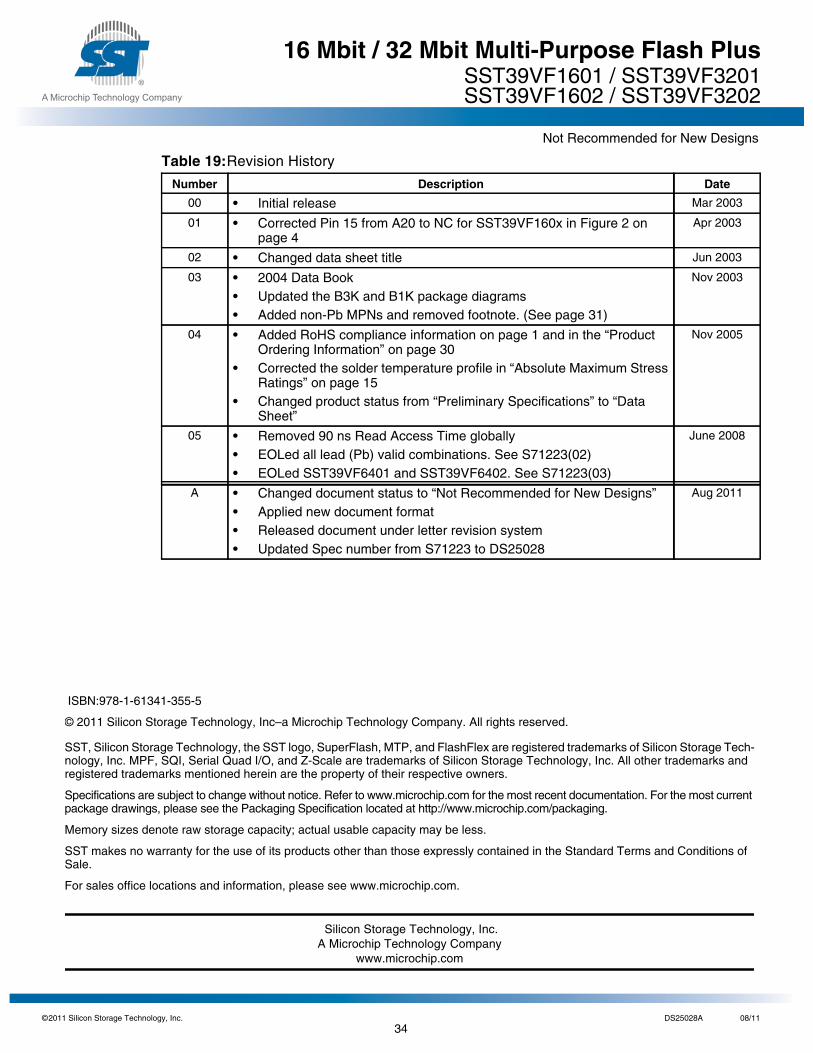
Table 19:Revision History
Number Description Date
00 • Initial release Mar 2003
01 • Corrected Pin 15 from A20 to NC for SST39VF160x in Figure 2 onpage 4
Apr 2003
02 • Changed data sheet title Jun 2003
03 • 2004 Data Book• Updated the B3K and B1K package diagrams• Added non-Pb MPNs and removed footnote. (See page 31)
Nov 2003
04 • Added RoHS compliance information on page 1 and in the “ProductOrdering Information” on page 30
• Corrected the solder temperature profile in “Absolute Maximum StressRatings” on page 15
• Changed product status from “Preliminary Specifications” to “DataSheet”
Nov 2005
05 • Removed 90 ns Read Access Time globally• EOLed all lead (Pb) valid combinations. See S71223(02)• EOLed SST39VF6401 and SST39VF6402. See S71223(03)
June 2008
A • Changed document status to “Not Recommended for New Designs”• Applied new document format• Released document under letter revision system• Updated Spec number from S71223 to DS25028
Aug 2011
© 2011 Silicon Storage Technology, Inc–a Microchip Technology Company. All rights reserved.
SST, Silicon Storage Technology, the SST logo, SuperFlash, MTP, and FlashFlex are registered trademarks of Silicon Storage Tech-nology, Inc. MPF, SQI, Serial Quad I/O, and Z-Scale are trademarks of Silicon Storage Technology, Inc. All other trademarks andregistered trademarks mentioned herein are the property of their respective owners.
Specifications are subject to change without notice. Refer to www.microchip.com for the most recent documentation. For the most currentpackage drawings, please see the Packaging Specification located at http://www.microchip.com/packaging.
Memory sizes denote raw storage capacity; actual usable capacity may be less.
SST makes no warranty for the use of its products other than those expressly contained in the Standard Terms and Conditions ofSale.
For sales office locations and information, please see www.microchip.com.
Silicon Storage Technology, Inc.A Microchip Technology Company
www.microchip.com
ISBN:978-1-61341-355-5
11 Silicon Storage Technology, Inc. DS25028A 08/11
34
Recommended