
Niko Kangas
A Comparison of High-Level Synthesis
and Traditional RTL in Software and
FPGA Design
Technology and Communication
2020

2
VAASAN AMMATTIKORKEAKOULU
UNIVERSITY OF APPLIED SCIENCES
Tietotekniikka
TIIVISTELMÄ
Tekijä Niko Kangas
Opinnäytetyön nimi Korkean tason synteesin ja perinteisen RTL:n vertailu
ohjelmisto- ja FPGA-suunnittelussa
Vuosi 2020
Kieli englanti
Pages 89 + 2 liitettä
Ohjaaja Santiago Chavez (VAMK), Petri Ylirinne (Vacon Oy)
Tämä opinnäytetyö tehtiin Vacon Oy:lle, joka on osa Danfossin Drives-segmenttiä.
Opinnäytetyön tarkoituksena oli vertailla uutta Vitis-työkalua nykyisesti käytössä
oleviin, Vivadoon ja SDK:hon, joilla suunnitellaan FPGA-piirejä sekä ohjelmistoja.
Työ antaisi puoleettoman näkemyksen kummastakin suunnitteluvuosta, ja auttaisi
hahmottamaan niiden kustannustehokkuuksia.
Työssä toteutettiin ledin kirkkauden ohjaus kummallakin vuolla, ja niitä verrattiin
keskenään. Vertailussa oli tarkoituksena tuoda esille eri toteutuksien koko, tehon-
kulutus, verifioinnin helppous ja käytetty aika.
Tietoa etsittiin tieteellisistä artikkeleista, julkaisuista sekä ohjelmistojen ja
laitteiden valmistajan manuaaleista ja dokumentaatiosta.
Työssä todettiin, ettei Vitis-työkalulla voida toteuttaa tehtävänannon mukaista to-
teutusta. Sen sijaan uudeksi vertailukohteeksi otettiin Vivado HLS-työkalu.
Vertailusta selvisi, että molemmat vuot käyttävät lähes saman verran resursseja ja
tehoa. Algoritmin verifiointiprosessi on myös helpompaa HLS-vuossa. HLS-to-
teutus kuitenkin tuotti pientä viivettä jatkuvassa ajossa, joten sitä ei pitäisi käyttää
aikakriittisissä käyttötarkoituksissa.
HLS:llä ei voida täysin korvata perinteistä vuota, mutta se voisi soveltua parem-
minkin käyttökohteisiin, joissa vaaditaan suurta laskentatehoa, eikä vaadi aika-
kriittistä toiminnallisuutta.
Keywords FPGA, High Level Synthesis, HLS, Xilinx, Vitis

3
VAASAN AMMATTIKORKEAKOULU
UNIVERSITY OF APPLIED SCIENCES
Tietotekniikka
ABSTRACT
Author Niko Kangas
Title A Comparison of High-Level Synthesis and Traditional RTL
in Software and FPGA Design
Year 2020
Language English
Pages 89 + 2 appendices
Name of Supervisor Santiago Chavez (VAMK), Petri Ylirinne (Vacon Oy)
This thesis was done for Vacon Oy, which is a part of Danfoss's Drives segment.
The aim of the thesis was to compare the new Vitis tool with those currently in use,
Vivado and SDK, which are used to design FPGA circuits and software. The thesis
would give an objective look into both design flows and could help to understand
their cost-effectiveness.
The thesis was carried out by creating an LED brightness control program with both
flows and they were compared to each other. The aim of the comparison was to
bring up the size of both implementations, the power consumption, the ease of ver-
ification and the time spent.
Information was sought in scientific articles, publications, and software and hard-
ware manufacturer manuals and documentation.
During the course of the thesis it was concluded that Vitis cannot be used to imple-
ment the specified functionality. Instead, the Vivado HLS tool was introduced as a
new benchmark.
The comparison revealed that both flows use nearly the equal amount of resources
and power. The algorithm verification process is also easier using the HLS flow.
However, the HLS implementation introduced a small delay between runs and
therefore it should not be used in timing-critical applications.
The traditional flow should not be entirely replaced with HLS, however it could be
more suitable for intensive mathematical algorithms that do not require time-critical
functionality.
Keywords FPGA, High Level Synthesis, HLS, Xilinx, Vitis

4
CONTENTS
TIIVISTELMÄ
ABSTRACT
1 INTRODUCTION .......................................................................................... 12
1.1 Background ............................................................................................. 12
1.2 Objective of the thesis ............................................................................. 13
1.3 Structure of the thesis.............................................................................. 13
1.4 Danfoss ................................................................................................... 14
1.5 Frequency converter................................................................................ 14
2 RELEVANT TECHNOLOGIES AND TOOLS ............................................ 16
2.1 FPGA ...................................................................................................... 16
2.1.1 RTL ............................................................................................. 17
2.1.2 HLS ............................................................................................. 19
2.2 Zynq-7000 SoC ....................................................................................... 21
2.3 PWM ....................................................................................................... 23
2.4 Vivado Design Suite ............................................................................... 23
2.4.1 Main features ............................................................................... 24
2.5 Xilinx SDK ............................................................................................. 27
2.5.1 Basic features .............................................................................. 28
2.6 Xilinx Vitis.............................................................................................. 30
2.6.1 Vitis IDE ..................................................................................... 30
2.7 Vivado HLS ............................................................................................ 32
2.7.1 Vivado HLS IDE ......................................................................... 32
2.8 Advanced eXtensible Interface (AXI) .................................................... 33
2.8.1 AXI Interconnect ......................................................................... 36
3 DESIGN FLOWS ........................................................................................... 37
3.1 Vivado design flow ................................................................................. 37

5
3.1.1 Create design ............................................................................... 39
3.1.2 Simulate design ........................................................................... 39
3.1.3 Assign design constraints ............................................................ 39
3.1.4 Synthesis and implementation .................................................... 39
3.1.5 Export to SDK and develop software.......................................... 40
3.2 Vitis application acceleration flow ......................................................... 40
3.2.1 Features and architecture............................................................. 40
3.2.2 Obstacles for using Vitis in FPGA design .................................. 43
3.3 Vivado HLS design flow ........................................................................ 44
4 IMPLEMENTATION .................................................................................... 45
4.1 The PWM program ................................................................................. 45
4.2 Traditional RTL and software implementation....................................... 48
4.2.1 Creating the IP............................................................................. 48
4.2.2 Configuring the PS ...................................................................... 52
4.2.3 Managing connections ................................................................ 53
4.2.4 Simulating the design .................................................................. 53
4.2.5 Assigning the PWM output to an LED ....................................... 56
4.2.6 Synthesis and implementation .................................................... 57
4.2.7 Developing the software ............................................................. 59
4.3 Implementing the design with HLS ........................................................ 63
4.3.1 Validating the algorithm with a C testbench ............................... 63
4.3.2 Configuring the IP ....................................................................... 65
4.3.3 Synthesis ..................................................................................... 66
4.3.4 C/RTL cosimulation and exporting the IP .................................. 68
4.3.5 Managing connections and configurations ................................. 71
4.3.6 Developing the software ............................................................. 73
5 COMPARING THE TWO WORKFLOWS .................................................. 78
5.1 Resource utilization and power consumption ......................................... 78
5.2 Time consumed ....................................................................................... 79
5.3 Migrating designs to an ASIC or other manufacturer’s tools ................. 82
6 CONCLUSIONS ............................................................................................ 84

6
6.1 Potential futher research ......................................................................... 85
REFERENCES ...................................................................................................... 86
LIST OF FIGURES AND TABLES
Figure 1, Danfoss logo /3/ .................................................................................... 14
Figure 2, Danfoss Drives product line /3/ ............................................................ 15
Figure 3. Basic FPGA architecture /5/ ................................................................. 17
Figure 4. Example circuit /7/ ................................................................................ 18
Figure 5. VHDL description of above-mentioned circuit /7/ ................................ 19
Figure 6. An example of a high-level data flow specification /9/ ......................... 20
Figure 7. An example of a possible RTL implementation of the specification above
/9/ .......................................................................................................................... 21
Figure 8. The evaluation board connected into a base board .............................. 22
Figure 9, 50%, 75% and 25% duty cycle examples /12/ ....................................... 23
Figure 10. GUI of the Vivado Design Suite .......................................................... 24
Figure 11. Block design view ................................................................................ 25
Figure 12. Example view of IP packager .............................................................. 25
Figure 13. Waveform window in the simulation tool /12/ ..................................... 26
Figure 14. Synthesis utilization report /14/ .......................................................... 27
Figure 15. Xilinx SDK GUI /15/ ........................................................................... 28
Figure 16. Example view of Xilinx SDK and some of its features /16/ ................. 29
Figure 17. Debugging view in Xilinx SDK /16/ .................................................... 29
Figure 18. Vitis IDE default perspective /18/ ....................................................... 31
Figure 19. Workspace in Vitis Analyzer /18/ ........................................................ 32
Figure 20. Vivado HLS GUI /19/ .......................................................................... 33
Figure 21. Channel architecture of writes /20/ ..................................................... 35
Figure 22. AXI4-Lite control signals in a write transaction /21/ ......................... 36
Figure 23. AXI Interconnect core diagram, /22/................................................... 36

7
Figure 24. Xilinx Vivado design flow /23/ ............................................................ 38
Figure 25. Vitis Unified Software Platform elements /18/ .................................... 41
Figure 26. Descriptions of the build targets in Vitis /18/ ..................................... 42
Figure 27. Architecture of a Vitis accelerated application /18/ ........................... 42
Figure 28. A flowchart visualizing the program’s operation. .............................. 47
Figure 29. AXI IP creation wizard ........................................................................ 48
Figure 30. Included design source files ................................................................ 49
Figure 31. Counter and comparator handling processes ..................................... 50
Figure 32. Ports and Interfaces view .................................................................... 50
Figure 33. Included software drivers and source code files ................................. 51
Figure 34. Graphical view of the resulting IP ...................................................... 51
Figure 35. Address range of the PWM generator module .................................... 52
Figure 36. Zynq PS ............................................................................................... 52
Figure 37. Zynq’s clock configuration view ......................................................... 52
Figure 38. Diagram showing the block design ..................................................... 53
Figure 39. Block diagram for the simulation ........................................................ 54
Figure 40. Functionality of the counter ................................................................ 54
Figure 41. Simulation with 50% pulse width ........................................................ 55
Figure 42. Simulation with 0% pulse width .......................................................... 55
Figure 43. Simulation with 100% pulse width ...................................................... 56
Figure 44. XDC file ............................................................................................... 56
Figure 45. Block design with debugging IP included ........................................... 57
Figure 46. RTL representation of the PWM generator module ............................ 58
Figure 47. Utilization report of the implementation ............................................. 58
Figure 48. Power consumption estimate of the implementation ........................... 59
Figure 49. Timing summary of the implementation .............................................. 59
Figure 50. Pulse width control software ............................................................... 60
Figure 51. Software cycling the pulse width ......................................................... 61
Figure 52. Fixed pulse width value in SDK .......................................................... 62
Figure 53. Hardware debugger view in Vivado ................................................... 62
Figure 54. LED with a 35% pulse width ............................................................... 62

8
Figure 55. LED with a 5% pulse width ................................................................. 63
Figure 56. PWM signal generation function in Vivado HLS ................................ 64
Figure 57. Test bench code 1 ................................................................................ 65
Figure 58. C simulation successful ....................................................................... 65
Figure 59. AXI interface configurations in Vivado HLS....................................... 66
Figure 60. Test bench code 2 ................................................................................ 67
Figure 61. Synthesized interfaces ......................................................................... 67
Figure 62. Register address information .............................................................. 68
Figure 63. C/RTL cosimulation waveform ............................................................ 70
Figure 64. Synthesized VHDL file ......................................................................... 70
Figure 65. PWM signal with 50% pulse width ..................................................... 71
Figure 66. Block design with the HLS IP .............................................................. 72
Figure 67. XDC file in the HLS block design ....................................................... 72
Figure 68. Utilization of the HLS implementation ................................................ 72
Figure 69. Power consumption estimate of the HLS implementation ................... 73
Figure 70. Module initialization function ............................................................. 74
Figure 71. Pulse width control function ............................................................... 75
Figure 72. Write transaction of 25% pulse width ................................................. 76
Figure 73. Pulse width of 25% on the LED .......................................................... 76
Figure 74. Pulse width of 5% on the LED ............................................................ 76
Table 1. Comparison of resource utilization ........................................................ 78
Table 2. Comparison of estimated power consumption ....................................... 79
Table 3. Comparison of required time .................................................................. 80

9
LIST OF..APPENDICES
APPENDIX 1. HLS driver initialization function ............................................... 90
APPENDIX 2. HLS driver functions ................................................................... 91

10
LIST OF ABBREVIATIONS
ALU Arithmetic logic unit
API Application programming interface
ASIC Application Specific Integrated Circuits
AXI Advanced eXtensible Interface
BRAM Block RAM
BSP Board support package
CLB Configurable logic block
DSP Digital signal processing
FF Flip-flop
FPGA Field-programmable gate array
GPIO General-purpose input/output
GUI Graphical user interface
HDL Hardware description language
HLS High-Level Synthesis
HW Hardware
I/O Input and output
IC Integrated circuit

11
IDE Integrated development environment
IP Intellectual property
LED Light-emitting diode
LUT Look-up table
PL Programmable logic
PLL Phase-locked loop
PS Processing system
PWM Pulse-width modulation
RAM Random-access memory
RTL Register-transfer-level
SDK Software development kit
SOC System on chip
UART Universal Asynchronous Receiver/Transmitter
VHDL Very High Speed Integrated Circuit Hardware De-
scription Language
VIP Verification Intellectual Property
XDC Xilinx Design Constraints
XRT Xilinx Runtime

12
1 INTRODUCTION
1.1 Background
There is a rising trend on the market towards increasing abstraction in field-pro-
grammable gate array (FPGA) design. What this means in practice, is that the de-
sign is programmed entirely using a high-level language, for example, in C, C++ or
Python. The used software tool’s compiler will then translate the code into a register
transfer level (RTL) implementation automatically, without the need for the user to
have any knowledge about FPGA design and VHDL, which is a hardware descrip-
tion language. This design flow is called HLS (High-Level Synthesis). Tradition-
ally, all this has been done by first implementing the FPGA block in VHDL on the
RTL and then programming the controlling software using C or C++. Essentially,
the HLS design flow enables the developer to do both phases using their preferred
programming language.
Xilinx is one of the leading semiconductor and FPGA manufacturers and most im-
portantly, the inventor of the FPGA. On the 1st of October 2019, Xilinx announced
the Vitis Unified Software Platform, a new, free and open source tool for HLS de-
velopment. One of the main reasons why Xilinx has developed this tool is that they
want to provide developers the possibility to utilize hardware (HW) with common
programming languages they understand, because modern computer architectures
can be difficult to work with, and understanding and utilizing CPUs, GPUs and
FPGAs well requires a lot of hardware expertise. /1/
Every used resource consumes real space on the FPGA chip. Thus, it is clearly im-
portant to optimize the resource usage in the design. When manufacturing an FPGA
chip out of the implementation designed on an evaluation board, all of the logic not
in use is stripped from the final product. Therefore, every cent of increased cost
accumulates into a large amount of money when the number of shipped products is
in hundreds of thousands, or even millions. In other words: the smaller the chip, the
more efficient the cost.

13
1.2 Objective of the thesis
The aim of this thesis is to compare these two workflows for Vacon Oy. The goal
is to find out what the HLS implementation is like and which of the workflows is
the most efficient one to use. The factors being compared include the time con-
sumed, ease of verification and the size of the implementation. The comparison is
done by creating a PWM program, which will be used to control the brightness of
an LED (Light-emitting diode). It is also important to regard if HLS in fact does not
require the engineer to have any knowledge about FPGA design.
The traditional workflow utilizes Xilinx Vivado Design Suite and Xilinx Software
Development Kit, which are used to design the FPGA block design and the control-
ling software, respectively.
At first, the objective was to implement the entire HLS implementation using only
Xilinx’s Vitis tool. After a while of researching it was discovered that it cannot be
done with Vitis alone. That is because Vitis cannot access the physical hardware
pins and only manages the data flow between a host software and a kernel on the
FPGA. This will be explained in more detail in chapter 3.2 Then, the best course
of action was to research, whether an other Xilinx tool, Vivado HLS, would work.
According to HLS’s documentation it can be used to develop IPs using C, C++ or
SystemC. What this means in practice is that HLS replaces the part where develop-
ers would traditionally code the IP in VHDL, with C. HLS also enables the devel-
oper to test the algorithm using a test bench written in C, before needing to perform
RTL simulation. The rest of the flow including creation of the control software us-
ing Xilinx SDK remains the same. /2/
1.3 Structure of the thesis
The second chapter of the thesis describes the relevant technologies and tools for
the thesis. The third chapter describes the design flows. The fourth chapter de-
scribes the implementation of the PWM program using both RTL and software, and

14
HLS workflows. The fifth chapter is for comparing these two workflows. The sixth
chapter includes the conclusions of the thesis and potential research for the future.
1.4 Danfoss
Danfoss is a Danish family-owned company founded in 1933, that operates in sev-
eral segments around the world. The segments include expertise in heating, cooling,
power solutions and drives. Danfoss employs more than 28,000 people and has fac-
tories in over 100 countries. /3/
Danfoss Drives is the segment that manufactures frequency converters. Vacon
(founded 1993 in Vaasa) became a part of Danfoss Drives in December of 2014,
and the combination has made Drives one of the world’s leading frequency con-
verter manufacturers. The combination of forces also opened new possibilities for
Vacon to invest further in R&D and sales. /3/
Figure 1, Danfoss logo /3/
1.5 Frequency converter
Frequency converters, or AC drives, are used to control the speed of an electrical
motor. This enables the enhancing of process control, energy consumption reduc-
tion, decrease of mechanical stress and optimization of the operation of electric
motor-controlled applications.
Frequency converters have multiple uses, including converting energy from the sun,
wind or tides and transmitting it into the electrical network, combining energy
sources and storages to create energy management solutions, elevators, pumps and
cranes. When used in cranes or elevators, they can be equipped with brakes to
smoothly reduce the controlled motor’s speed.

15
For Danfoss, the environment is a key driver in the development of AC drives. Be-
cause more than 50% of electrical energy consumption comes from the use of elec-
trical motors, AC drives have a key role in reducing global emissions. If AC drives
were used in every suitable application, global electricity consumption could be
reduced by up to 10%. While they are barely seen, they contribute a lot at making
the world more sustainable. /3/
Figure 2, Danfoss Drives product line /3/
16
2 RELEVANT TECHNOLOGIES AND TOOLS
This chapter describes the relevant technologies and tools used in this thesis.
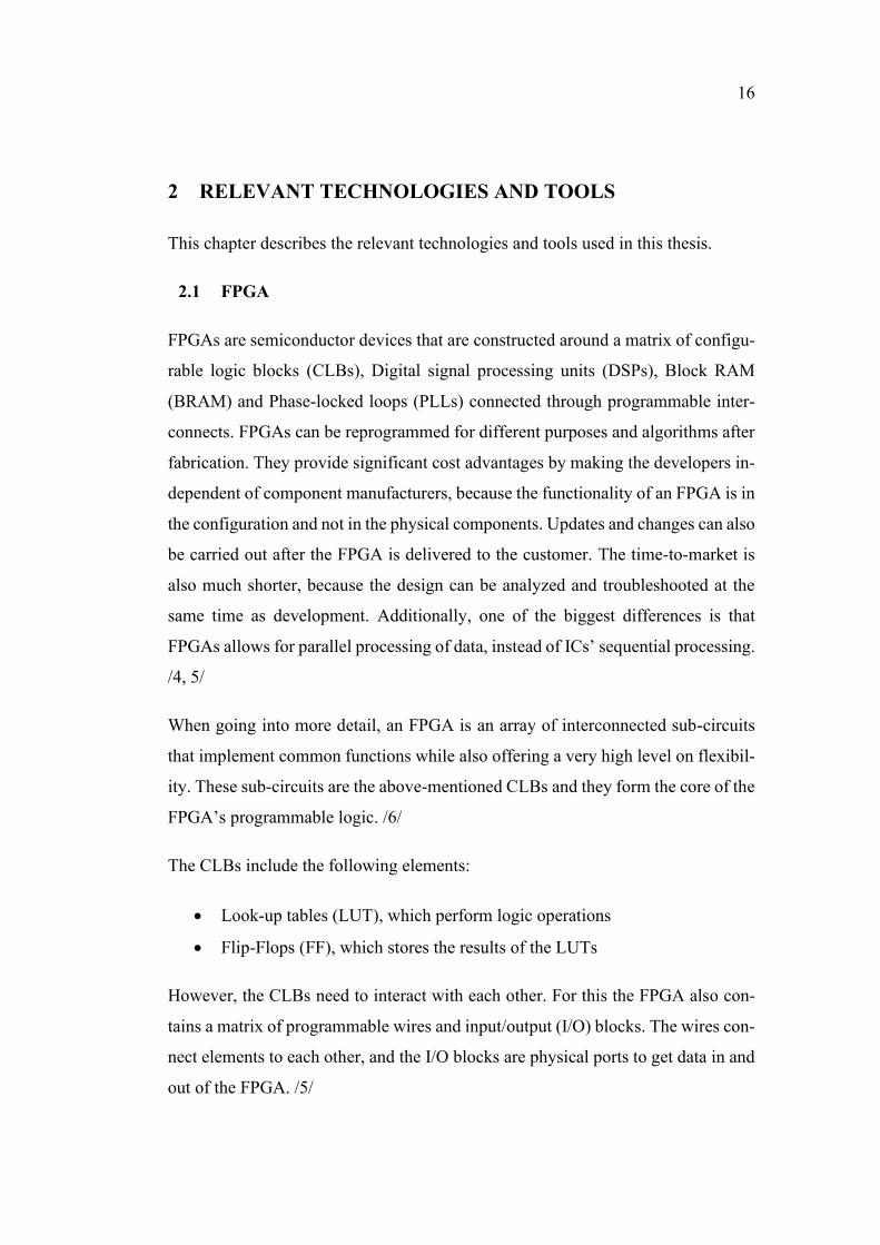
2.1 FPGA
FPGAs are semiconductor devices that are constructed around a matrix of configu-
rable logic blocks (CLBs), Digital signal processing units (DSPs), Block RAM
(BRAM) and Phase-locked loops (PLLs) connected through programmable inter-
connects. FPGAs can be reprogrammed for different purposes and algorithms after
fabrication. They provide significant cost advantages by making the developers in-
dependent of component manufacturers, because the functionality of an FPGA is in
the configuration and not in the physical components. Updates and changes can also
be carried out after the FPGA is delivered to the customer. The time-to-market is
also much shorter, because the design can be analyzed and troubleshooted at the
same time as development. Additionally, one of the biggest differences is that
FPGAs allows for parallel processing of data, instead of ICs’ sequential processing.
/4, 5/
When going into more detail, an FPGA is an array of interconnected sub-circuits
that implement common functions while also offering a very high level on flexibil-
ity. These sub-circuits are the above-mentioned CLBs and they form the core of the
FPGA’s programmable logic. /6/
The CLBs include the following elements:
• Look-up tables (LUT), which perform logic operations
• Flip-Flops (FF), which stores the results of the LUTs
However, the CLBs need to interact with each other. For this the FPGA also con-
tains a matrix of programmable wires and input/output (I/O) blocks. The wires con-
nect elements to each other, and the I/O blocks are physical ports to get data in and
out of the FPGA. /5/

17
An I/O block consists of different components, including pull-up/pull-down resis-
tors, buffers and inverters. The FPGAs program is stored in SRAM cells that define
the functionality of the CLB. /6/ The combination of these elements form the basic
FPGA architecture shown in Figure 3 below:
Figure 3. Basic FPGA architecture /5/
2.1.1 RTL
Register-transfer level (RTL) is part of digital circuit design, and a typical part in
modern digital design. It is a design abstraction, which models a circuit regarding
the flow of data signals between hardware registers and the logical operations exe-
cuted on those signals. RTL abstraction is used in hardware description languages
(HDLs), such as VHDL and Verilog, to create descriptions of a circuit, from which
lower-level representations and actual wiring can be derived RTL abstraction is a
part of the FPGA design flow, which will be demonstrated later. /7/

18
A synchronous circuit consists of registers, which utilize sequential logic, and com-
binational logic. Registers are the only elements in the circuit to have memory prop-
erties, and they synchronize the circuit’s operation to the clock cycles’ edges. They
consist of a parallel combination of flip-flops. Combinational logic is a type of dig-
ital logic which is implemented by Boolean circuits, where the output depends en-
tirely on the present input and it typically consists of logic gates Combinational
logic then executes all the logical functions in the circuit. /7, 8/
In Figure 4, a very simple synchronous circuit is shown. The inverter is connected
from the register’s output Q to the register’s input D. This creates a circuit which
changes its state on every rising edge of the clock clk. In addition to the register,
the combinational logic consists of the inverter /7/.
Figure 4. Example circuit /7/
However, when designing real-world digital integrated circuits, the designs are
commonly written with an HDL at a higher level of abstraction. The engineer de-
clares the registers and describes the combinational logic in HDLs by using if-else
-like constructs and arithmetic operations. This is the level, which is called the reg-
ister-transfer-level. The term RTL meaning that it focuses on describing the
stream of the signals between registers. In the case of RTL, registers roughly cor-
respond to variables in programming languages. /7/
Figure 5 shows the above-mentioned circuit described in VHDL:

19
Figure 5. VHDL description of above-mentioned circuit /7/
Additionally, in FPGA design, software is used alongside RTL abstraction. While
RTL is utilized to describe the functionality of the circuit, a software application
can be created to complement the FPGA design. The software application can, for
example, perform more complex calculations and then feed the results to the RTL
design, and handle communications.
2.1.2 HLS
Creating a behavioral description of hardware in a high-level programming lan-
guage, like C or C++, forms the basis of HLS. Next the HLS compiler translates the
created hardware specification code into an RTL implementation. /5/
High-level synthesis provides the following benefits:
• Verification at C-level provides much faster validation of the algorithm than
RTL verification.
• Improved system performance for software designers (They can accelerate
the most intensive parts of their algorithms by compiling on the FPGA.)
• Creation of different implementations of the source code using optimization
directives.
• Developers only need to focus on the algorithm and not the hardware-level
implementation, which is synthesized automatically. /5/
HLS also possesses some limitations:

20
• In more complex designs, the algorithm must be written in a particular style
to make the synthesis tool utilize parallelism
o C algorithms should not be directly translated with HLS, because it
can cause poor performance
• RTL produced by HLS is very difficult to follow
o Any problems on the synthesized RTL can be difficult to pinpoint
In the following example, a simple high-level data flow specification is shown.
Variables x1 and x2 carry the values from the + and – operators to an another +
operator, which outputs y:
Figure 6. An example of a high-level data flow specification /9/
In Figure 7, a possible RTL implementation is shown, when the high-level specifi-
cation code is fed into the HLS compiler:

21
Figure 7. An example of a possible RTL implementation of the specification above
/9/
In the above-mentioned RTL example, the following steps have been taken:
• The variables have been assigned to registers
• Operations have been assigned to function units
• The controller schedules the operations to occur on a certain clock cycle.
2.2 Zynq-7000 SoC
The Zynq-7000 family is based on the Xilinx System on Chip (SoC) architecture.
These boards feature an ARM Cortex-A9 based CPU and Xilinx 28nm program-
mable logic in a single device. The evaluation board used in this thesis is the MYIR
Tech MYC-C7Z020, which is based on the Zynq-7000 SoC. It includes the Xilinx’s
dual-core Cortex-A9 processor and an Artix-7 FPGA. The Artix-7 family is typi-
cally used in cost-sensitive, low power applications where serial transceivers and
high DSP and logic throughput is required. /10/
The processing system (PS) of the MYIR Tech evaluation board include the fol-
lowing elements:
• ARM Cortex-A9 dual core processor
o 677 MHz

22
• On-Chip Memory
o 1GB DDR3 SDRAM
o 4GB eMMC
o 32MB Flash memory
• Linux 3.15.0 OS support
• I/O peripherals
o 10/100/1000M Ethernet
o LEDs
o 2x serial ports
o 2x I2C
o ADC
o JTAG
The programmable logic (PL) includes the following elements:
• Artix-7 FPGA subsystem
o 85 000 logic cells
▪ 53 200 LUTs
▪ 220 DSPs
The evaluation board (blue) connected into a Vacon’s base board is shown in Figure
8:
Figure 8. The evaluation board connected into a base board

23
2.3 PWM
Pulse width modulation is a type of a digital signal. It is used to create a square
wave by switching the signal’s state to high and low (on and off). This pattern sim-
ulates voltage values between these two states by changing the amount of time the
signal spends on versus the time it spends off. The duration of time when the signal
is “on” or “high”, is called the pulse width, or duty cycle. By changing the pulse
width, the signal gets varying analog values, the average voltage, between the two
states. /11/
For example, if the “high” state is set to 5 Volts and “low” is set to 0 Volts, and
pulse width is set to 50%, the resulting output voltage value is 2.5V. Correspond-
ingly, by setting the pulse width to 100% the resulting output would be 5 Volts. In
Figure 9 below, visual representation of different pulse widths, or duty cycles, are
shown:
Figure 9, 50%, 75% and 25% duty cycle examples /12/
PWM can be used to control the frequency and voltage supplied to an AC motor.
2.4 Vivado Design Suite
Vivado Design Suite is a Xilinx development system for implementing designs into
Xilinx programmable logic devices. It includes the IP integrator tool, which is used

24
to create embedded hardware. IP integrator is used in this thesis to create a custom
PWM signal generator block. The PWM block is then configured in VHDL on the
RTL by setting a fixed frequency of 1000 Hz and connecting the PWM signal to an
LED. The graphical user interface (GUI) of the Vivado Design Suite is shown in
Figure 10:
Figure 10. GUI of the Vivado Design Suite
2.4.1 Main features
All of the main features are accessible from the starting view. These features in-
clude:
• IP integrator
• Simulation
• Synthesis and implementation
• Hardware manager

25
The block design view is used to add the Zynq processing system and the PWM
generator block to the design, and to manage connections. The view is shown in
Figure 11:
Figure 11. Block design view
The PWM block is created using the IP integrator’s IP packaging tool, which cre-
ates an AXI IP. An example view in the IP packaging tool is as follows:
Figure 12. Example view of IP packager

26
The simulation tool includes the Waveform window, which can be used to monitor
signals and analyze simulation results by, for example:
• Running the simulation to verify the design functionality
• Adding signals to monitor their status
• Changing signal and wave properties to review the signals
• Using markers and cursors to highlight important events in the simulation
• Using zoom and time measurement functionalities
An example view of the Waveform window is shown in Figure 13. /12/
Figure 13. Waveform window in the simulation tool /12/
The synthesis and implementation tools are used to transform an RTL design into a
gate-level representation. The tool provides data of the implementation’s use of de-
vice resources, power consumption and timing. /13/ As we can see in Figure 14, the
generated utilization report shows the utilization of an example implementation,
including the used LUTs and Flip-Flops:

27
Figure 14. Synthesis utilization report /14/
2.5 Xilinx SDK
Xilinx Software Development Kit (SDK) is a tool based on the Eclipse open-source
framework, and is used to develop software applications for embedded hardware.
It directly interfaces to the Vivado embedded hardware design environment. In this
thesis, the SDK is used to develop the software which varies the created PWM gen-
erator’s pulse width. An example view of the SDK’s GUI is shown in Figure 15.

28
Figure 15. Xilinx SDK GUI /15/
2.5.1 Basic features
The Xilinx SDK enables the developer to:
• Create board support packages
• Develop applications
• Debug code
• Interact with the hardware created in Vivado
The Xilinx SDK has the integrated development environment (IDE) of Eclipse,
which is familiar to many software developers. It has the well-known common fea-
tures of Eclipse IDE shown in Figure 16.

29
Figure 16. Example view of Xilinx SDK and some of its features /16/
The SDK’s debugging view is shown in Figure 17.
Figure 17. Debugging view in Xilinx SDK /16/

30
One of the most important features in the SDK for this thesis is that the Vivado
simulation waveform view can be utilized on the SDK. The developer can set break-
points and force certain values to the variables in the SDK, and set triggers in the
Vivado Hardware Manager to make the program stop on certain conditions and then
visualize what is happening on the PL.
2.6 Xilinx Vitis
The Xilinx Vitis unified software platform is a tool that unifies every aspect of Xil-
inx software development into a single platform. What this means is that it can be
used for the same case as the Xilinx SDK is used in this thesis in the embedded
software development. In addition to this, Vitis also supports application accelera-
tion flow, which enables software developers to accelerate the most performance-
intensive parts on the FPGA. /17/
Right at the start it can be seen that the embedded software development flow in-
volves no HLS, because it is designed to replace SDK with Vitis for developing
software. So, the next course of action was to take a look into the acceleration flow.
This chapter describes the basics of the IDE itself. The reasons why it was eventu-
ally concluded that it is not possible to create a design entirely in high-level lan-
guage by only using Vitis, are went through in chapter 3. /17/
2.6.1 Vitis IDE
The default view of the Vitis is quite similar to SDK. That is no surprise, because
Vitis is Eclipse-based aswell.

31
Figure 18. Vitis IDE default perspective /18/
The default view basically includes all of the main features:
• Software emulation
• Hardware emulation
• Hardware execution
• Vitis Analyzer
The IDE includes the Vitis Analyzer, which is a powerful debugging tool for view-
ing application timelines, waveforms system summaries and guidance on optimiz-
ing the design. Figure 19 shows an example workspace in the Analyzer.

32
Figure 19. Workspace in Vitis Analyzer /18/
2.7 Vivado HLS
Xilinx Vivado HLS is a tool that transforms a C specification into an RTL imple-
mentation which is synthesized into an FPGA. Vivado HLS is also Xilinx’s imple-
mentation of an HLS compiler. It a very similar programming environment as any
other designed for application development. It shares technology with other proces-
sor compilers for the interpretation, analysis and optimization of C and C++ pro-
grams. The main difference is that the Vivado HLS compiler targets an FPGA as
the execution fabric. /5/
2.7.1 Vivado HLS IDE
The IDE of Vivado HLS is graphically very straightforward. The software has just
a couple functions to it, all of which can be accessed from the main screen. A newly
created project is shown in Figure 20.

33
Figure 20. Vivado HLS GUI /19/
The four main features of Vivado HLS are highlighted at the top of the window in
Figure 20:
• C-simulation
• C Synthesis
• C/RTL cosimulation
• Export RTL.
2.8 Advanced eXtensible Interface (AXI)
AXI is a part of a family of microcontroller buses, ARM AMBA (Advanced Mi-
crocontroller Bus Architecture). It is a widely adopted interface protocol in Xilinx
products. /20/
There are three types of AXI4 interfaces:
• AXI4 (high-performance memory-mapped requirements)
• AXI4-Lite (simple, low-throughput communication)
• AXI4-Stream (high-speed streaming of data). /20/

34
The major benefit of standardizing on the AXI bus is that developers only need to
learn a single protocol for IPs. The AXI4-Lite interface is used in this thesis due to
the lightweight nature of the logic to be implemented, and the Lite interface is the
simplest of the three. /20/
The simplest description of the AXI interface is that it connects a single AXI master
and AXI slave to each other, which exchange information. In this case, the PWM
generator IP acts as an AXI slave, and the Zynq PS acts as a master. Data can move
in both directions between the master and slave simultaneously and data transfer
sizes can vary. However, AXI4-Lite only allows for one data transfer per transac-
tion, but it is enough, because the only data needed to be transferred is the pulse
width value. /20/
The interface consists of five different channels:
• Read address channel
• Write address channel
• Read data channel
• Write data channel
• Write response channel. /20/
The separate data and address connections for reads and writes provides simultane-
ous and bidirectional data transfer.
Figure 21 shows an example write transaction, which includes the write address,
data and write response channels.

35
Figure 21. Channel architecture of writes /20/
The PWM implementation in this thesis only utilizes the write transaction, so let’s
take a closer look at it. A signal port called WDATA, which resides in the write
data channel, contains the data that the software sends to the PWM generator mod-
ule. Because this port may contain more data in addition to the pulse width value,
there are four control signals which indicate that the data inside WDATA port is
significant /21/:
• AWREADY (Write address channel)
o Indicates that the slave is ready to accept an address.
• WVALID (Write data channel)
o Indicates that valid write data is available.
• WREADY (Write data channel)
o Indicates that the slave can accept the data.
• BVALID (Write response channel)
o Indicates that a valid write response is available./21/
Figure 22 shows the control signals in action, when the value “70000004” is sent:

36
Figure 22. AXI4-Lite control signals in a write transaction /21/
2.8.1 AXI Interconnect
The AXI Interconnect is a block which connects one or more AXI memory-mapped
master devices to one or more slave devices. Figure 23 shows the AXI Interconnect
core block diagram.
Figure 23. AXI Interconnect core diagram, /22/
Inside the core, a crossbar core routes traffic between the master and slave inter-
faces. Along each pathway between the interfaces, additional AXI cores can per-
form various conversion and buffering functions.

37
3 DESIGN FLOWS
The used design flows, including the traditional RTL flow and the newer HLS flow,
will be described in this chapter. The Vitis tool will also be looked into, and it will
be explained why it could not be used to create the specified functionality.
3.1 Vivado design flow
In the case of the traditional RTL and software flow, the PWM program is split into
two parts. The following lists includes the two parts and the used tools:
• Hardware implementation
o Vivado Design Suite
• Software
o Xilinx SDK
Next, the design is then implemented with HLS:
• Hardware implementation
o Vivado HLS
o Vivado Design Suite
• Software
o Xilinx SDK
The entire Vivado design flow is shown in Figure 24:

38
Figure 24. Xilinx Vivado design flow /23/
The first part, hardware implementation, includes creating the PWM generation
module in VHDL, configuring the processing system, simulating and verifying the
design, connecting the PWM output signal to an LED and managing other connec-
tions, synthesis and implementation. All of this is done in Vivado.
Figure 24 also includes “C-Based Design with High-Level Synthesis”. This repre-
sents the development of the PWM module with HLS, which will replace VHDL
with C-language using the Vivado HLS tool, and the rest of the flow remains nearly
the same. This will be demonstrated later.

39
3.1.1 Create design
During the design creation process, the PWM module is created by using the AXI4-
Lite IP creation wizard. The resulting IP is then configured in VHDL to generate a
PWM signal in accordance with the specification.
Next, the Zynq PS is added to the block design and configured accordingly. Vivado
automatically manages most of the connections and adds any required additional
IPs to aid with the functionality, for example a processor system reset IP and the
AXI Interconnect.
3.1.2 Simulate design
The design is then simulated to verify the functionality of the PWM module using
the AXI Verification IP. In this case the VIP acts as an AXI master that writes data
to the PWM module, which acts as an AXI slave.
3.1.3 Assign design constraints
Next, the PWM signal output is connected to an LED by assigning a constraint in a
Xilinx Design Constraints (XDC) file. Timing, placement and synthesis constraints
can also be assigned at this point to help improve design performance. They can be,
for example, period constraints for clock signals, placement constraints for each
type of logic element and synthesis constraints which control how the synthesis tool
processes and implements FPGA resources. However, in this particular scenario,
the only constraint needed is the connection between the PWM output signal and
an LED. /24/
3.1.4 Synthesis and implementation
After that, the design is synthesized from HDL sources into a design netlist, which
contains both logical design data and constraints. When synthesis is complete, de-
sign implementation can be run, which converts the logical design into a physical
40
bitstream file that can be downloaded on to the FPGA. The resulting implementa-
tion includes timing, resource and power consumption reports. /24/
3.1.5 Export to SDK and develop software
The second part of the PWM program is the software that varies the created signal’s
pulse width and sends the value to a register’s memory address in the PWM module
every 10 ms. The software is created in Xilinx SDK. When the hardware bitstream
is generated and exported to the SDK, the resulting project contains the required
drivers for the IPs and software libraries, which are a part of the board support
package (BSP)generated from the bitstream.
After the software is ready to run, the hardware bitstream is downloaded to the
FPGA device and the software is run on the board’s ARM processor. The software
can be stored on the RAM or flash memory. The running implementation can then
be debugged in Vivado and SDK by utilizing the JTAG connection.
3.2 Vitis application acceleration flow
The Vitis acceleration flow provides a framework for software developers to de-
velop applications using their preferred high-level programming language, and to
accelerate them on an FPGA. The acceleration takes place on a hardware compo-
nent, called kernel, which can be developed on C, C++, OpenCL C or RTL to be
run on the FPGA. The software component, the host program, runs on an embedded
processor, for example, the ARM A9 processor on the Zynq board, and is written
in C or C++. The host program communicates with the kernel using OpenCL API
calls.
3.2.1 Features and architecture
Vitis provides a variety of accelerated libraries, including AI, image processing and
video transcoding. /18/
Figure 25 shows the following elements and features of the Vitis platform:

41
Figure 25. Vitis Unified Software Platform elements /18/
• A target platform
o Such as Xilinx Alveo Data center accelerator cards or Zynq boards,
on which the kernel is developed.
• XRT (Xilinx Runime)
o Connects the host program to the target platform and handles the
transactions between the program and kernel(s) with an API.
• Vitis core development kit
o Provides the tools for the software development.
• Vitis accelerated libraries
o Provide FPGA acceleration with common functions of math, statis-
tics, linear algebra and DSP and use specific applications. /18/
As mentioned in chapter 2.6.1, three of Vitis’s main features are build targets called
Software Emulation, Hardware Emulation and Hardware Execution. The two emu-
lation modes are used for validation and debugging, and the system hardware target
is used to generate the FPGA binary into the device. /18/
The features can be seen in Figure 26.

42
Figure 26. Descriptions of the build targets in Vitis /18/
The architecture of a Vitis accelerated application is shown in Figure 27:
Figure 27. Architecture of a Vitis accelerated application /18/
Figure 27 depicts the functionality between a host program and a kernel. Let’s im-
agine a scenario where the developer has concluded that the software has a partic-
ularly intensive function, which requires to be run faster or is a bottleneck in the
software. The function is then set to be run on a kernel on the FPGA. /18/
For example, if this were implemented on the Zynq board, the host program would
be running on the ARM processor and the kernel on the PL. The execution model
can be separated into the following steps:
• Host program writes the data in to the global memory of the device through
the AXI bus.
• Host program sets up the kernel with input parameters.

43
• Host program triggers the execution of the kernel on the FPGA.
• Kernel performs the required function while reading data from global
memory.
• Kernel outputs data back to global memory and notifies the host.
• Host program reads data from global memory and continues processing. /18/
3.2.2 Obstacles for using Vitis in FPGA design
Without going into any more detail on the build process of the application and ker-
nels, let’s go through the obstacles that prevent the use of this flow.
The target platform, which in this case would be based on the Zynq board, is created
in Vitis. However, the platform creation requires an XSA hardware specification
file, which is generated by Vivado, that represents the hardware implementation of
the block design. Xilinx provides sample platforms for Zynq devices, but the de-
veloper can also create them manually. Nonetheless, this directly contradicts the
theory that both, the hardware and software, could be created entirely in Vitis only
using C-language.
The kernel is created to be run on the hardware platform. While the kernel has in-
puts and outputs, they are used for communicating with the host application through
the global memory, and not with any external hardware pins. This is the second and
final obstacle, which led to the conclusion that Vitis alone cannot be used for im-
plementing the specified PWM functionality. The only use case Vitis can be used
in is to replace SDK as the IDE in software development. /17, 18/
Even if it were somehow possible to implement the specified PWM functionality
with Vitis alone, it would require an unnecessary amount of extra work. First, the
documentation does not indicate at any point that the Vitis is intended for this kind
of use, or that it is even possible. Second, Vivado HLS already exists for the purpose

44
of developing IPs with high-level languages and the documentation includes tuto-
rials for this. To summarize, using Vivado HLS is the recommended approach if
HLS development is required. /9/
While Xilinx promotes Vitis as a platform which requires no expertise in hardware
or FPGA design, this is actually correct, as Vitis does not involve the creation of
hardware at all. Their statement means that software developers can access the per-
formance of FPGAs and utilize it in the most computation-intensive parts in their
software, without actually having any technical knowledge about them. /1/
3.3 Vivado HLS design flow
As mentioned in chapter 3.2, the design flow in Vivado HLS remains much the
same as with the traditional RTL flow. The differences are in creating the IP and
simulating the design. One must keep in mind however, that synthesis in HLS
means translating the C code into HDLs, and not synthesizing the design into a
netlist, which is a step taken in Vivado, and can be confusing. The steps taken in
Vivado HLS are shown here:
• The PWM signal generation algorithm is coded entirely in C.
• The algorithm is tested and simulated with a C testbench.
• The algorithm is synthesized into an RTL representation.
• The RTL representation is simulated using C/RTL co-simulation.
o Verifies the synthesized RTL using the C testbench.
o Simulation waveforms can be output to Vivado simulator.
• The finished design can then be exported to Vivado as an IP. /23/
Additionally, the software side has some differences. Mainly that the IP needs to be
initialized and started manually using drivers. In any case, Figure 24 in chapter 3.1
applies to HLS as well.

45
4 IMPLEMENTATION
In this chapter the PWM program is described, verified and implemented. The tra-
ditional RTL and software flow will be implemented first, and second the HLS
flow.
4.1 The PWM program
The aim of the program is to generate a PWM signal that controls an LED’s bright-
ness with a sweeping pulse width. The PWM signal is configured with a fixed fre-
quency of 1000 Hz, which translates to a 1 millisecond (ms) period. The pulse width
starts at 0% and is then varied every 10 ms by 1% until it reaches 100%. Then, the
pulse width starts to decrease by 1% every 10 ms until it reaches 1%. As a result
the LED appears to have a slow “breathing” effect.
A period of 1 ms is achieved by creating a counter variable named counter, which
goes from 0 to a set maximum value and resets after 1 ms. First, the clock frequency
on the evaluation board is set to 100 MHz, when a clock cycle is performed every
10 nanoseconds. A millisecond consists of 1 000 000 nanoseconds. The following
calculation results in the required counter’s maximum value:
1 000 000 𝑛𝑠
10 𝑛𝑠= 100 000
After the counter’s maximum value is clear, the next step is to simulate the pulse
width. For example, to achieve a 1% pulse width, a limit variable called pulse_width
needs to be created with a value of 1% of the counter’s maximum. In this case, it
would be 1000.
So, the counter is initialized and set to 0 and the PWM signal output defaults to
high. When the counter reaches the pulse width limit the program switches the
PWM signal’s state to low, until the counter reaches its maximum value. Then it
resets and starts counting again from 0.

46
One of the program’s requirements was to change the pulse width by 1% every 10
ms, so the pulse_width is increased every 10 ms by 1000. Figure 28 shows a
flowchart to visualize the PWM program’s operation:

47
Figure 28. A flowchart visualizing the program’s operation.

48
As the program’s requirements state, the pulse width needs to decrease 1% at a time
after it has reached 100%. This means that the same principle needs to be imple-
mented as with the increasing pulse width, but with the pulse_width variable de-
creasing instead of increasing by 1000 every 10 periods until it reaches 0. Then it
starts to increase again until 100 and so on.
4.2 Traditional RTL and software implementation
At this point the traditional implementation of the PWM program is demonstrated.
4.2.1 Creating the IP
The implementation begins with creating the project and selecting the correct part
which represents the evaluation board. After this is done the project is ready. The
next step is to create an AXI4-Lite IP, which will become the PWM generator mod-
ule. The AXI IP creation wizard has the following options:
• Choose between master and slave
• The type of interface, for example, stream or lite.
• Number of registers
Figure 29. AXI IP creation wizard
For this use case only one register is needed, and that is for the pulse width value,
but the minimum amount of registers is 4 so that is fine.

49
After the IP creation is complete, the wizard directs us to a separate window where
the programming of the IP happens. The newly created IP includes two source files:
Figure 30. Included design source files
The top-level file includes all of the physical port descriptions, including the control
signals included in the AXI interface, and any potentially customizable parameters.
In this case, only the PWM output port needs to be added.
The lower-level file includes the description of the PWM generator’s logic, which
consists of the following things (corresponding signal and variable declarations in-
cluded):
• A counter from 0 to 100000
signal counter : unsigned
(C_S_AXI_DATA_WIDTH-1 downto 0); constant PWM_COUNTER_MAX : integer := 100000;
• PWM output signal and port
signal pwm : std_logic := '0'; PWM_output : out std_logic;
• A register called slave register 0 for writing the pulse width data from the
software
signal slv_reg0 :std_logic_vector(C_S_AXI_DATA_WIDTH-1
downto 0);
• Counter handling process
o Increases the counter value one by one until it reaches its maximum,
then it is reset
• Comparator handling process
o Compares the counter value to the register’s value and sets the PWM
signal value accordingly

50
The processes are shown here:
Figure 31. Counter and comparator handling processes
After the PWM generation is written, the IP is ready for packaging, after which the
IP can be connected to the Zynq PS. From the Package IP tab the newly created
output port can be seen:
Figure 32. Ports and Interfaces view

51
The software drivers to be created and the source code files can also be viewed in
the tab:
Figure 33. Included software drivers and source code files
And finally, the graphical representation of the resulting IP:
Figure 34. Graphical view of the resulting IP
After packaging of the IP, the address range of the newly created IP can be viewed
in IP integrator. When the slave registers are created along with the IP, their ad-
dresses are offset every 4 bytes: 0x00, 0x04x, 0x08, 0x12 and so on. Since the used
register is slave register 0, its address is the first address in the range shown in
Figure 35, 0x43C00000:

52
Figure 35. Address range of the PWM generator module
4.2.2 Configuring the PS
When the IP is packaged, it is ready to be added to the design, along with the Zynq
PS. The Zynq PS block looks like as shown here:
Figure 36. Zynq PS
The clock used to control the PWM module is the FCLK_CLK0 as seen in Figure
35. The clock is connected to the AXI master GP0 clock seen on the left side of the
PS. As the program’s specification states, the FCLK clock frequency needs to be
set to 100 MHz:
Figure 37. Zynq’s clock configuration view

53
Another mandatory configuration was to select the correct DDR memory compo-
nent on the PS.
4.2.3 Managing connections
After the PS is configured accordingly, the next step is to manage all the connec-
tions, of which the majority is handled automatically by Vivado. The connection
automation tool connects the Zynq PS to the PWM module with the AXI interface
while utilizing the AXI Interconnect, which is automatically added to the design in
case more AXI interfaces are required. The only connection needed to make man-
ually is to create a physical output port for the PWM signal output. Additionally,
Vivado adds a PS reset block for reset functionalities. Figure 38 depicts the created
block design:
Figure 38. Diagram showing the block design
4.2.4 Simulating the design
At this point the IP is ready for simulation. The simulation is made easy with the
AXI VIP, which was used by starting the IP creation wizard where instead of choos-
ing the option to edit an IP, the verification of the IP was chosen. This creates a new
block design which includes the verification IP and a sample AXI IP. The IP can

54
be deleted from the design and replaced with our PWM generator module. The be-
havioral simulation can now be started. The block diagram looks as depicted below:
Figure 39. Block diagram for the simulation
At this point, a testbench for the VIP could be created. While, the VIP only supports
SystemVerilog language for the testbench, it was possible to move forward with
forcing certain pulse width values in the graphical simulator view instead, because
the only variable that affects the functionality of the PWM signal is the pulse width.
However, with more complex designs, creating a testbench would simplify the ver-
ification process tremendously.
First, the simulation is run for 5ms with pulse width set to 50000, which is 50% of
the counter’s maximum value and it results as a 50% pulse width in the PWM output
signal.
Figure 40. Functionality of the counter
From the Figure 40, two things can be seen:
• Counter works as expected, resetting at its set maximum and starts from 0.
• PWM output signal is synchronized to clock signal’s rising edges

55
When zooming out a bit, the effect of the set pulse width value can be seen clearly:
Figure 41. Simulation with 50% pulse width
The program’s specification stated that the period of the PWM signal is 1 ms. In
Figure 41 above, there are 2 markers set to measure the time the PWM signal is
high, which is 500 microseconds, or 0,5ms. This seems to be functioning correctly,
as the pulse width was set to 50%.
Next, two more things need to be verified: Will the PWM signal go fully low with
0% pulse width, and fully high with 100% pulse width. First, simulation for 5 ms
with 0% pulse width:
Figure 42. Simulation with 0% pulse width
The reason I was concerned about the 0% pulse width is that the PWM generator
code states that the comparator process first checks if the counter value is lower
than the pulse width value and primarily wants to set the PWM signal to high, but
as seen in Figure 42, the PWM signal in fact stays at low state.
As for the PWM signal’s reaction to 100% pulse width, the simulation with 50%
pulse width shown in Figure 41 indicates that the PWM signal does not go high
when the counter is at 0, but when its value is at 1. This something that needs to be
verified with 100% pulse width, so that the signal truly remains at high state. Below,
simulation with 100% pulse width is shown:

56
Figure 43. Simulation with 100% pulse width
As seen in Figure 43, the PWM signal does in fact stay at high state with 100%
pulse width. When thinking about it, it makes sense, because when the counter
reaches 99999, the comparator process checks if it is less than the pulse width value,
which it is, and remains at high. Then the counter is reset to 0 due to being at its
maximum and the IP continues doing its work.
The implementation can also be simulated post-synthesis and post-implementation
to see if the synthesis or implementation result alters the functionality of the design.
In this scenario it was concluded to be unnecessary, since the design is quite simple.
It is sufficient to have Vivado only run the timing analysis to see, whether the design
can be run with the set 100 MHz clock frequency.
4.2.5 Assigning the PWM output to an LED
After the design’s functionality is verified by simulation, the PWM output port is
ready to be connected to an LED. To do this, an XDC file needs to be created with
the following contents:
Figure 44. XDC file
The upper row assigns the PWM output port to a pin called L20. This pin is assigned
to an LED, which I discovered from Vacon’s sample project. The lower row spec-
ifies an I/O standard, which informs the tool what kind of a voltage the pin is using.
It can also be used to specify the drive strength and slew rate, which determine the
57
output impedance and maximum rate of change of output voltage per unit of time,
respectively.
4.2.6 Synthesis and implementation
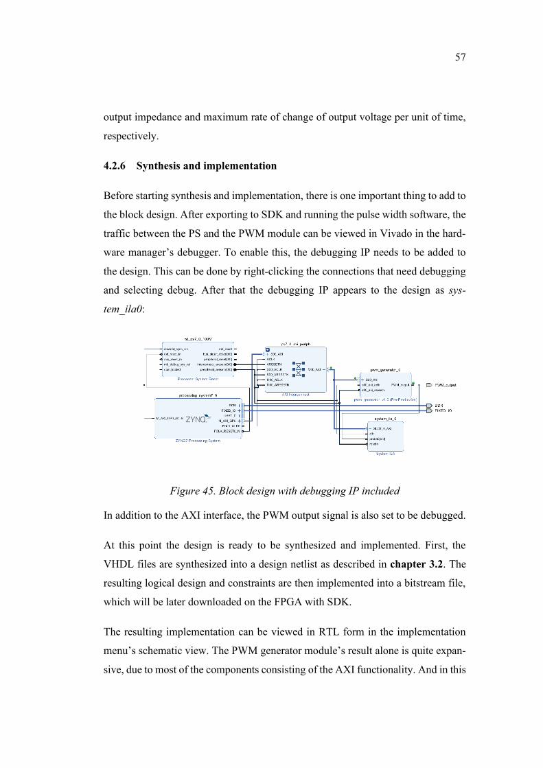
Before starting synthesis and implementation, there is one important thing to add to
the block design. After exporting to SDK and running the pulse width software, the
traffic between the PS and the PWM module can be viewed in Vivado in the hard-
ware manager’s debugger. To enable this, the debugging IP needs to be added to
the design. This can be done by right-clicking the connections that need debugging
and selecting debug. After that the debugging IP appears to the design as sys-
tem_ila0:
Figure 45. Block design with debugging IP included
In addition to the AXI interface, the PWM output signal is also set to be debugged.
At this point the design is ready to be synthesized and implemented. First, the
VHDL files are synthesized into a design netlist as described in chapter 3.2. The
resulting logical design and constraints are then implemented into a bitstream file,
which will be later downloaded on the FPGA with SDK.
The resulting implementation can be viewed in RTL form in the implementation
menu’s schematic view. The PWM generator module’s result alone is quite expan-
sive, due to most of the components consisting of the AXI functionality. And in this

58
case, it is not useful to examine it thoroughly. The module’s RTL schematic is
shown in top-down view below:
Figure 46. RTL representation of the PWM generator module
The implementation’s resource utilization report is as follows:
Figure 47. Utilization report of the implementation
As we can see from the report, the resulting implementation is quite lightweight.
Same can be seen from the power consumption estimation report:

59
Figure 48. Power consumption estimate of the implementation
As the power consumption report indicates, the large majority (95%) of the power
is used by the PS. Both reports will be compared to the HLS implementations re-
ports in a later chapter.
The timing report includes a summary of the timing constraints set automatically
by Vivado, when the clock frequency was set to 100 MHz. The report indicates that
the design works as expected:
Figure 49. Timing summary of the implementation
When the bitstream has been generated, the design is ready to be exported to SDK
for developing the software.
4.2.7 Developing the software
After exporting the bitstream to SDK, the BSP is generated, which includes the
software libraries and device drivers. In this case, the software creation process is

60
quite simple. The PWM generator module requires no manual control or initializa-
tion whatsoever.
The software that controls the pulse width is simple. It is written in C-language and
has the following components:
• Increase and send pulse width value by 1% every 10 ms until it reaches
100%
• Decrease and send pulse width value by 1% every 10 ms until it reaches 0%
Going more into detail, the software has two for loops, one for increasing and the
other for decreasing the pulse width. When starting the program, the first loop starts
by sending its default value, 0%, to the slave register’s memory address and then
waits for 10 ms using a sleep function, after which the pulse width value is increased
by 1%. Then the process is repeated until the pulse width reaches 100% and then
the program proceeds to the second loop and executes until it reaches 0%. The code
can be seen here:
Figure 50. Pulse width control software

61
Because the nature of the entire design is very simple and has only function, the
software was possible to be made using a sleep function. Essentially, this halts the
execution of the whole software for 10 ms and nothing else can be executed during
this time, but this implementation does it job, which is to be simple.
If there were more functionalities in the design, for example, communications with
Ethernet or fieldbuses, the LED blinking part of the software would make any of
the communications impossible, due to the sleep function pausing the entire pro-
gram. If this was indeed a more complex design, the write transaction of the pulse
width value should be implemented with an interrupt, that interrupts the program to
send the data every 10 ms and then resumes executing other functions in the soft-
ware.
Moving on, the next step is to connect the evaluation board into the PC using a
JTAG-connection, which allows the SDK to program the FPGA with the bitstream
file and to download the software on the RAM. Additionally, the JTAG-connection
makes it possible to simultaneously debug the design in Vivado by viewing any
required signals in a waveform, and in SDK. After the FPGA has been programmed,
the LED starts pulsing, and the data traffic is then examined in Vivado. The result
of running the software is shown in Figure 50:
Figure 51. Software cycling the pulse width
The functionality can be examined closer by setting a fixed pulse width value in
SDK’s debugger and viewing the write transaction for the pulse width value. For
example, setting a fixed 35000 pulse width value in SDK results in a 35% pulse
width.

62
Figure 52. Fixed pulse width value in SDK
The transaction where this value is sent to the slave register is seen in Vivado:
Figure 53. Hardware debugger view in Vivado
From Figure 53 it can be seen that the write transaction is successful, by looking at
the control signals. Comparing to AXI4-Lite’s documentation (Figure 22) they
seem to be functioning as expected. Lastly, the resulting pulse width’s effect can be
seen on the LED:
Figure 54. LED with a 35% pulse width
When comparing to a 5% pulse width, the LED gets visibly dimmer:

63
Figure 55. LED with a 5% pulse width
From the previously mentioned results it can be stated that the implementation func-
tions as specified.
4.3 Implementing the design with HLS
This chapter describes the implementation of the PWM program using Vivado
HLS, Vivado and SDK.
4.3.1 Validating the algorithm with a C testbench
The very first step when starting a design in HLS is to select a part and define a
clock signal’s period. The clock frequency specified is 100 MHz, so the period
would be 10 ns. The next step is to develop the PWM generation algorithm and
verify its functionality with a C testbench. As mentioned before, this provides a
much faster verification of the algorithm compared to RTL verification, because
this way the algorithm can be verified without needing to create the RTL imple-
mentation first. In the traditional flow, the developer also needs to create every sig-
nal and port that is required.
The algorithm’s general functionality is the same as with the RTL version. A coun-
ter is compared to the pulse width value and PWM signal output is set accordingly.
If the counter reaches its cap, it is reset to 0. For testing purposes, a result variable
is created to resemble the resulting pulse width that the algorithm outputs with the
PWM signal.
In HLS, the IP to be created is a single function in C code. The function declaration
includes the inputs and outputs

64
The pulse_width variable acts as an input that sends the pulse width value to the IP.
The *pwm variable acts as an output port that outputs the PWM signal. In HLS the
output ports need to be declared as pointers. The above-mentioned result variable
is returned to the testbench when this function is called. The function is shown here:
Figure 56. PWM signal generation function in Vivado HLS
The function is now ready for testing. HLS documentation states, that the simula-
tion is considered successful, if the testbench returns 0. Anything else will cause
the simulation to issue a fail message. /25/
The testbench used includes the following components:
o Three pulse width values to be sent to the PWM generator: 0%, 50% and
100%
o Three result variables, where the pulse width output by the generator func-
tion is sent
o An if statement to check if the returning pulse width values are correct
o Returns 0 if correct
o Returns anything else than 0 if it fails, in this case, 1
The testbench code is shown in Figure 57:

65
Figure 57. Test bench code 1
After running the C simulation, the simulation appears to be successful:
Figure 58. C simulation successful
Vivado HLS documentation also recommends as a good practice to compare test
bench results with golden data, which is a file that contains the correct results. In
this kind of a simple design, the testing performed is sufficient.
4.3.2 Configuring the IP
The code is almost ready for synthesis. After the algorithm’s functionality is vali-
dated, the last steps to do is to remove the result variable from the code, so that it
will not consume unnecessary resources, and to configure the IP as an AXI slave.
The function can also be changed to void function, as there are no return values to
it. This procedure can be risky, but the changes were minimal, and the simulation
later showed that the algorithm was working as expected.

66
Additionally, resulting IP needs to be configured as an AXI slave, like the RTL IP
created before. This can be done by adding the following three pragmas into the
code:
Figure 59. AXI interface configurations in Vivado HLS
The first pragma creates the AXI slave port with the relevant control signals. The
second row creates the PWM signal output port without any protocols. If this row
were missing, in this case the port would be automatically implemented using
ap_vld protocol, which includes a valid port to indicate the ready state of the port.
However, in this case it is not required. The third row implements the pulse width
input as a register and assigns a memory address to it.
4.3.3 Synthesis
Before running synthesis, the test bench code can be altered to better represent the
software that is used to control pulse width for verification purposes. The new
testbench is very similar to the one used in chapter 4.2.7, with the difference that
this test bench updates the pulse width every period, or 1 ms, rather than every 10
ms. The test bench is shown in Figure 60:

67
Figure 60. Test bench code 2
Now the design is ready to be synthesized from C to an RTL representation. The
synthesis process is rather quick, and it generates a report that includes performance
estimates, utilization estimates and generated interfaces.
Figure 61. Synthesized interfaces

68
As seen in Figure 61, the PWM signal output is correctly set as an output and the
AXI control signals can be seen. The generated VHDL files include information
about the registers’ addresses, including the pulse_width register:
Figure 62. Register address information
The address offset is 0x10 for the pulse width register, which makes the address
0x43C00010, if the same base address that was used with the RTL IP is used here.
The addresses include control signals to start the IP and other data signals. How-
ever, these addresses do not necessarily need to be used manually, because the gen-
erated drivers include functions that change these registers’ values.
4.3.4 C/RTL cosimulation and exporting the IP
After the synthesis is complete, the design can be simulated using C/RTL cosimu-
lation, which verifies that the synthesized RTL representation matches the C code.
This simulation also uses the C testbench. When the simulation is complete, the
logic can be examined in the Analysis tab. This tab helps to visualize what is hap-
pening on the RTL, as the HLS compiler synthesizes the design with complicated
variable names and the data routes are a bit hard to follow without graphical repre-
sentation. The process of the algorithm can be summarized as follows:
• Pulse width value is read

69
• A multiplexer handles the increase of the counter and the comparison to its
maximum and the pulse width value
• The counter value is compared to the read pulse width value and PWM out-
put signal is written
The waveform of the simulation can be viewed in Vivado. When examining the
waveform, a potential negative effect of HLS synthesis can be seen:
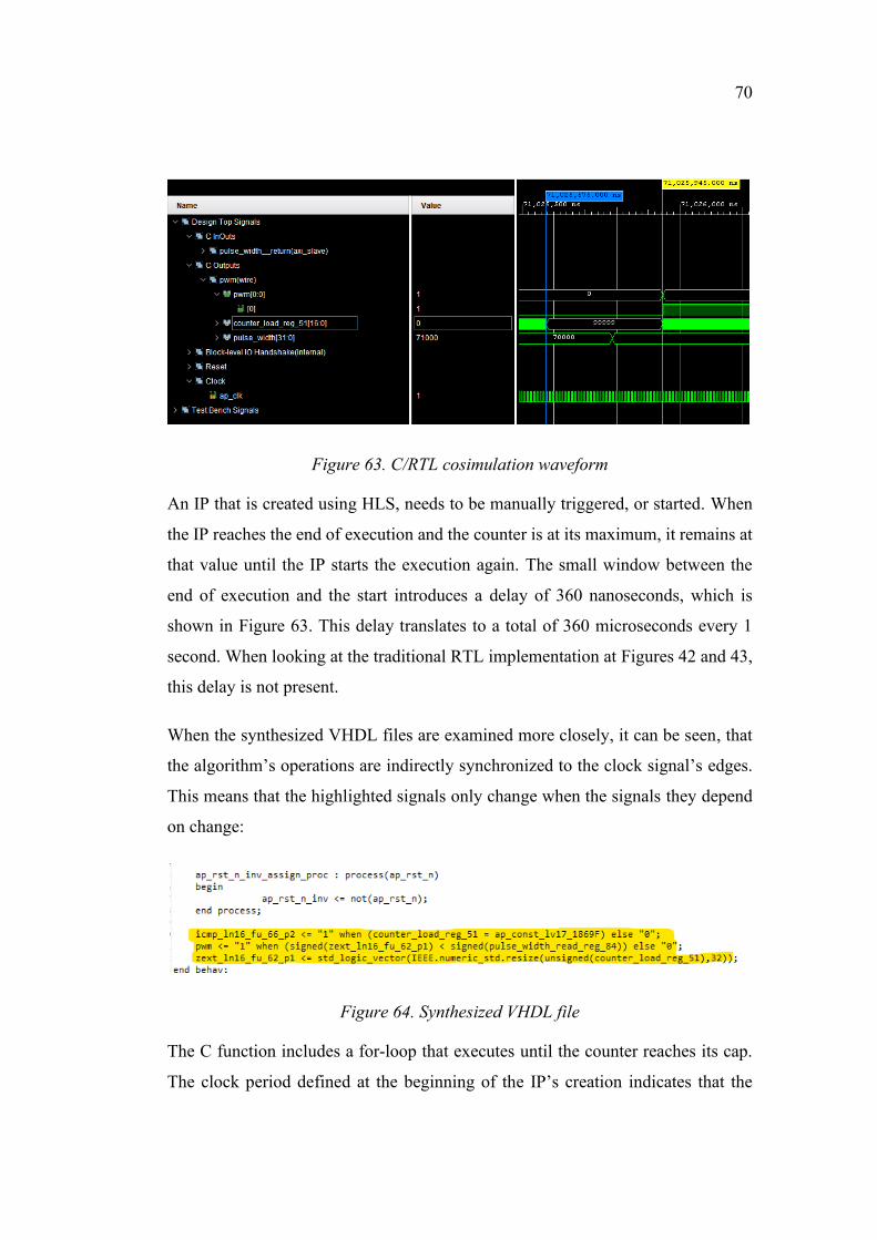
70
Figure 63. C/RTL cosimulation waveform
An IP that is created using HLS, needs to be manually triggered, or started. When
the IP reaches the end of execution and the counter is at its maximum, it remains at
that value until the IP starts the execution again. The small window between the
end of execution and the start introduces a delay of 360 nanoseconds, which is
shown in Figure 63. This delay translates to a total of 360 microseconds every 1
second. When looking at the traditional RTL implementation at Figures 42 and 43,
this delay is not present.
When the synthesized VHDL files are examined more closely, it can be seen, that
the algorithm’s operations are indirectly synchronized to the clock signal’s edges.
This means that the highlighted signals only change when the signals they depend
on change:
Figure 64. Synthesized VHDL file
The C function includes a for-loop that executes until the counter reaches its cap.
The clock period defined at the beginning of the IP’s creation indicates that the
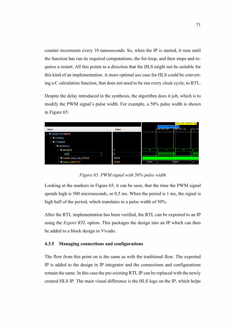
71
counter increments every 10 nanoseconds. So, when the IP is started, it runs until
the function has run its required computations, the for-loop, and then stops and re-
quires a restart. All this points to a direction that the HLS might not be suitable for
this kind of an implementation. A more optimal use case for HLS could be convert-
ing a C calculation function, that does not need to be run every clock cycle, to RTL.
Despite the delay introduced in the synthesis, the algorithm does it job, which is to
modify the PWM signal’s pulse width. For example, a 50% pulse width is shown
in Figure 65:
Figure 65. PWM signal with 50% pulse width
Looking at the markers in Figure 65, it can be seen, that the time the PWM signal
spends high is 500 microseconds, or 0,5 ms. When the period is 1 ms, the signal is
high half of the period, which translates to a pulse width of 50%.
After the RTL implementation has been verified, the RTL can be exported to an IP
using the Export RTL option. This packages the design into an IP which can then
be added to a block design in Vivado.
4.3.5 Managing connections and configurations
The flow from this point on is the same as with the traditional flow. The exported
IP is added to the design in IP integrator and the connections and configurations
remain the same. In this case the pre-existing RTL IP can be replaced with the newly
created HLS IP. The main visual difference is the HLS logo on the IP, which helps

72
at distinguishing the HLS IPs from RTL ones. Figure 66 shows the complete block
design with the HLS IP included:
Figure 66. Block design with the HLS IP
Since the PWM output port is named a bit differently, the XDC file needs to be
adjusted accordingly:
Figure 67. XDC file in the HLS block design
Next, the design is synthesized and implemented the same way the traditional de-
sign was. The generated resource and power reports are as follows:
Figure 68. Utilization of the HLS implementation

73
Figure 69. Power consumption estimate of the HLS implementation
These reports will be compared to the RTL implementation’s reports in chapter 5.
4.3.6 Developing the software
As stated before in chapter 4.3.4, an HLS IP needs to be started manually. This is
done by utilizing the IP’s drivers in the control software; therefore, the software
requires some additional driver functions:
• Config lookup function
o Checks if the corresponding device configuration can be found
• Config initialization function
o Checks if the device and the configuration can be found and sets the
IP’s state to ready
• Function that checks if the IP is ready
o Checks if the IP is ready for the next input
• IP start function (included in initialization, start and autorestart functions)
o Sets the start bit to 1 on the IP if it is ready
• IP auto-restart function

74
o Sets the auto-restart bit to 1 that automatically restarts execution af-
ter the IP has finished and is ready
• Set pulse width value function
o Sends the pulse width value to the IP’s register’s address
These functions’ prototypes are declared in the driver functions’ header file
xpwm_module.h and the functions’ implementations themselves are included in Ap-
penix 1 and 2. /19/
The software itself has two functions: An initialization function and the main func-
tion. The initialization function includes the lookup and initialization functions. /19/
The function is shown here:
Figure 70. Module initialization function
When called inside the main function, it first looks for the device configuration and
then proceeds to initialize it. Then it returns the status to the main function, where
the initialization is checked. If the setup was successful, the main function proceeds
to enable the auto-restart bit in the IP and then starts its execution:

75
Figure 71. Pulse width control function
As seen from the main function, the while loop functions exactly as with the tradi-
tional flow’s software. The only difference is that the HLS version of the IP pro-
vides a driver function that sends the pulse width data to the register, without the
need of knowing the address. This can also be done by sending the data to the ad-
dress manually.
Next the bitstream is downloaded to the FPGA, the software on the RAM, and the
data flow can be viewed in Vivado’s hardware manager afterwards. By forcing a
fixed 25000 pulse width value in SDK the result is as follows:

76
Figure 72. Write transaction of 25% pulse width
The resulting pulse width of 25% is seen on the LED, followed by a pulse width of
5%:
Figure 73. Pulse width of 25% on the LED
Figure 74. Pulse width of 5% on the LED
When letting the software cycle the pulse width value automatically, the LED ap-
pears to be pulsing as expected.
The point made in chapter 4.3.4 was that because the IP needs to be manually
started, there is a small delay between every period in the PWM signal. Although
the auto-restart bit can be enabled, the IP still has to wait for the ready bit to go high
before it can start again. This further reinforces the theory that HLS IPs are more
suitable for calculations that do not need to be run continuously.

77
As for the statement made at the introduction chapter that HLS does not need any
knowledge about FPGA design, this is false. This implementation would not be
possible to design without the knowledge about AXI bus, and the whole Vivado
design flow, including simulation, verification and configurations. But the case of
Vitis is a bit different since it does not involve the design of FPGAs themselves but
accessing their resources to boost the performance of software.

78
5 COMPARING THE TWO WORKFLOWS
The ultimate goal of this thesis was to find out how an HLS implementation com-
pares to an RTL implementation. The next step is to compare the two implementa-
tions’ resource utilization, power consumption and estimated time consumed.
5.1 Resource utilization and power consumption
After both of the designs were synthesized and implemented, Vivado generated re-
source utilization and estimated power consumption reports. Table 1 below shows
the difference between the usage of resources that were used a different amount in
the implementations:
Comparison of resource utilization (pcs)
RTL HLS Diff.(%)
LUT 431 457 6,0
FF 621 596 -4,0
Table 1. Comparison of resource utilization
From table 1 it can be seen that the resource utilization of both flows is really close
to each other, which is quite surprising. HLS automatically implements the RTL
implementation and it could be believed that it cannot be as efficient as the tradi-
tional RTL implementation. It can also be assumed that with RTL, the implemen-
tation’s efficiency in resource utilization has more to do with the skills of the de-
veloper than with HLS.
As for the resource usage itself, RTL possibly uses more FFs because the IP created
in Vivado included four pre-made registers by default, while the HLS IP included
only the one created manually. HLS’s higher use of LUTs, on the other hand, must
have something to do with the implementation itself, and the way the synthesized
RTL implementation handles the algorithm.

79
HLS also includes the possibility of declaring optimization directives that influence
the resulting RTL implementation. In a design this simple, however, there were no
suitable spots in the code to optimize. Possible targets of optimization in more com-
plex designs include, for example, function and loop pipelining, which allow the
operations to be implemented in an overlapping manner, and array partitioning,
which allows for splitting RAM blocks into multiple smaller arrays.
As for the estimated power consumption, the component that uses the majority
(95%) in both implementations is the processing system. Table 2 shows the total
power consumption difference between the implementations:
Comparison of estimated power con-
sumption (Watts)
RTL HLS Diff.(%)
Total 1,713 1,714 ~ 0
Table 2. Comparison of estimated power consumption
Looking at the results shown in table 2, the difference in power consumption is
quite negilible. If the design were a hundred or thousand times bigger, the difference
would undoubtedly be more relevant. When combining the information of both ta-
bles, the HLS implementation performed surprisingly well.
5.2 Time consumed
Next, the time consumed between the two flows is compared. The comparison is
measured in minutes and done by dividing the flows into smaller steps and estimat-
ing the required time to complete those steps. Table 3 represents the differences
between the design steps and the estimated required time for developing the spec-
ified PWM functionality. Each step is described in more detail after the table:

80
Design step RTL HLS
Coding the algorithm 60 min 30 min
Verifying the algorithm 45 min * 10 min
Verifying the implemen-
tation by simulation
- 15 min
Adding the IP to the de-
sign and configuring the
PS
15 min 15 min
Synthesis and implemen-
tation
5 min 5 min
Developing software 45 min 60 min
HW debugging 30 min 30 min
Total 200 min 165 min
*includes simulation
Table 3. Comparison of required time
In table 3, the first step specified is coding the algorithm. The estimated time re-
quired in this step include possible changes needed in the code.
The main difference here between the two flows is that with RTL there are simply
more lines of code. The RTL implementation includes two separate processes for
handling the PWM signal, and signal and port specifications in two separate files.
VHDL’s syntax is also much stricter than in C and it can take more time to get
everything right, for example, matching the data widths and handling type conver-
sions between signals that communicate with each other.

81
The next step includes the creation of a testbench on the HLS side, simulation on
the RTL side, and estimated time to make changes to the code after test runs. One
major benefit of HLS is that it allows the developer to verify the algorithm with a
C test bench and before RTL simulation. Not only is it much faster to make changes
to the code after each test run, C is also a more common programming language
and the RTL simulation is slow. RTL flow does, however, provide the possibility
of verifying the IP using an HDL test bench, but it would still require RTL simula-
tion of the IP.
While verifying the HLS design also requires simulating the synthesized RTL im-
plementation, it saves time to verify the algorithm itself beforehand. In table 3, the
time required at simulation for traditional RTL is included in the second step. The
next two steps are identical between the two flows, therefore the time required is
the same in these cases.
The final step that has differences is software development. In the case of HLS, the
IP requires more manual control than a traditional RTL one. The IP needs to be
manually initialized and started for each run by using the driver functions. Fortu-
nately though, all of the control functions include a ready check part inside them,
so that is handled automatically. Nevertheless, if HLS were used to create an IP that
performs certain computations and does not run continuously, the developer needs
to put extra work into managing the IP.
To summarize, it can be seen from table 3 that the HLS implementation was ap-
proximately 21% faster to develop. The use of resources and power was nearly the
same with both implementations.
It could be argued that the HLS flow might prove more useful in a much larger
implementation. That is because the design cycle is faster, and the gap between the
two flows could potentially increase as the design gets more complicated. Regard-
less, even though the HLS flow is faster and on par with the RTL flow in resource

82
usage, the delay between executions potentially makes it unsuitable for timing-crit-
ical uses, like controlling an electrical motor’s voltage and speed with PWM.
To make a secure choice between the two, more research needs to be done with
HLS, specifically about the use of optimization directives. But with the received
results so far, I would personally use HLS, as long as the implementation does not
require timing-critical performance.
5.3 Migrating designs to an ASIC or other manufacturer’s tools
One of the possible use cases of FPGAs is to design a circuit and then port the
design on to an ASIC. Xilinx provides platforms designed for ASIC prototyping,
and migrating designs created in Xilinx’s tools to ASICs can introduce technical
challenges, but migrating to other manufacturers’ devices and tools has legal obsta-
cles.
In the case of the traditional RTL implementation, the VHDL algorithm can be mi-
grated to an ASIC or other manufacturers’ FPGA design tools. There are naturally
device-specific coding styles among ASICs that require the modification of the
VHDL code to work on the target device, but no license agreement prevents this.
Using the code on other manufacturers’ tools is also possible, as long as it is purely
created by the developer. The developers who created the algorithm have every
right to use it the way they please.
However, Xilinx’s use agreement prevents the use of any software or bitstream
generated by Xilinx tools to develop designs for non-Xilinx devices. This concerns
RTL code synthesized by Vivado HLS. It does not prevent the developer of porting
ASIC designs to Xilinx devices for prototyping and verification. /26/
Consequently, if someone were to design an algorithm in C language and synthe-
sized it to an RTL implementation using Vivado HLS, the use agreement does not
allow said RTL code to be used in non-Xilinx tools or devices. The main motivation
behind this is most likely financial. Xilinx is the largest FPGA circuit manufacturer,

83
and wants to prevent any harm caused to their business. They openly let people use
their parts and tools as long as they are not used to allow competitors to take poten-
tial business away. Therefore, if one were to use Xilinx’s products to develop de-
signs, they are only to be used with Xilinx’s products.
These restrictions are further emphasized by the fact that Xilinx’s design tools are
all free to use, but cannot be used in conjunction with other manufacturers’ devices.
Their business approach is naturally to generate as much turnover as possible, by
selling as much devices as possible. Xilinx is also one of the few companies that
encourages schools to use their parts and tools for studies, but any thesis or paper
published that includes prohibited use of Xilinx’s tools or devices, while being as-
sociated to a school supported by Xilinx, may result in the removal of said support.
It is also important to note, that when testing a logic on an FPGA before migrating
it on an ASIC, one must consider that certain features may not even be available on
other vendors’ devices.
In summary, migrating designs between Xilinx devices only introduces technical
device-specific challenges, until other manufacturers’ devices or tools come into
the picture. It is possible to use Xilinx’s tools to develop code and use it anywhere,
as long as it is not generated by Xilinx’s tools in any way. Prototyping ASICs using
Vivado HLS is also much stricter, as the generated HLS code cannot be used with
non-Xilinx devices or tools.

84
6 CONCLUSIONS
The main goal of this thesis was to compare two design flows, RTL and HLS, both
of which was accompanied by a software. The comparison was done by developing
an LED controlling PWM program. The factors being compared were use of re-
sources, power consumption, ease of verification and time consumed.
The implementation using the traditional design flow went relatively smoothly.
However, the HLS flow was more of an issue, because the Vitis tool was first con-
cluded to be unable to perform the required task. After Vivado HLS was introduced
as a secondary option, the specified functionality was implemented successfully.
The used tools were quite complicated at the start and the amount of documentation
and tutorials is vast. After getting past the initial learning curve, the tools became
fun and much easier to use. In the case of Vitis, it took quite a long time to accept
that it might not be suitable for the specified task.
The comparison resulted in RTL’s favor due to the small delay introduced in the
HLS implementation, when the IP was run continuously. This result does not take
away from the fact, however, that HLS is perfectly capable of synthesizing a work-
ing RTL implementation, but for this particular implementation, the RTL version
is more robust.
At this point it seems that HLS is designed for translating C code into RTL, when
a developer already knows how to create an algorithm with C, or it is not worthwhile
to translate an existing algorithm to VHDL. To verify if HLS can replace RTL in
more mathematical use cases, more research needs to be done.
Compared to my personal expectations, the thesis panned out much better than ex-
pected. At first, the assignment felt quite daunting due to the very little amount of
FPGA courses in our university. However, because there was a practically endless
amount of documentation available, the only thing to prevent this from succeeding
was myself. The only way forward was to work hard.

85
Looking back, the terminology, theory and tools are much easier to understand after
actually implementing the designs. Personally, I consider myself to be a practical
person and I tend to learn much more by doing things myself. No matter how much
I read and research, it only matters so much until I get to use that information in
practice.
6.1 Potential futher research
A potential idea for further research could be investigating how HLS IPs can used
in conjunction with IPs made with traditional RTL. A good point to think about is
that if it is easier and more efficient to make certain computationally intensive al-
gorithms with HLS and the other parts with RTL that require continuous operation.
The comparison could also be repeated with a more complicated algorithm to see if
the faster design cycle difference gets even bigger, and if HLS could potentially
replace RTL in those scenarios. A particularly interesting matter in HLS is the ef-
fectiveness of the optimization directives.

86
REFERENCES
/1/ News article about the Vitis announcement. Accessed 6.2.2020.
https://www.xilinx.com/news/press/2019/xilinx-announces-vitis--a-unified-soft-
ware-platform-unlocking-a-new-design-experience-for-all-developers.html
/2 / Vivado HLS documentation (UG902). Accessed 24.4.2020.
https://www.xilinx.com/support/documentation/sw_manuals/xilinx2014_1/ug902-
vivado-high-level-synthesis.pdf
/3/ Danfoss website. Accessed 7.5.2020.
https://www.danfoss.com/en/
/4/ Xilinx website. Accessed 4.2.2020.
https://www.xilinx.com/products/silicon-devices/fpga/what-is-an-fpga.html/
/5/ Xilinx documentation (UG998). Accessed 7.2.2020.
https://www.xilinx.com/support/documentation/sw_manuals/ug998-vivado-intro-
fpga-design-hls.pdf
/6/ All about circuits website. “What is an FPGA?”. Accessed 4.2.2020.
https://www.allaboutcircuits.com/technical-articles/what-is-an-fpga-introduction-
to-programmable-logic-fpga-vs-microcontroller//
/7/ Wikipedia article. Accessed 4.2.2020.
https://en.wikipedia.org/wiki/Register-transfer_level/.

87
/8/ Tutorialspoint website. Accessed 4.2.2020.
https://www.tutorialspoint.com/computer_logical_organization/combina-
tional_circuits.htm/.
/9/ Sciencedirect article. Accessed 7.2.2020.
https://www.sciencedirect.com/topics/computer-science/high-level-synthesis/
/10/ Evaluation board description. Accessed 7.2.2020.
https://www.xilinx.com/products/boards-and-kits/1-79drxf.html
/11/ Arduino website. Accessed 4.2.2020.
https://www.arduino.cc/en/tutorial/PWM
/12/ Vivado documentation (UG937). Accessed 5.2.2020.
https://www.xilinx.com/support/documentation/sw_manuals/xilinx2014_1/ug937-
vivado-design-suite-simulation-tutorial.pdf Accessed 14.2.2020/
/13/ Vivado documentation (UG901), Accessed 14.2.2020.
https://www.xilinx.com/support/documentation/sw_manuals/xilinx2019_2/ug901-
vivado-synthesis.pdf
/14/ Xilinx tutorial video. Accessed 14.2.2020.
https://www.xilinx.com/video/hardware/synthesizing-the-design.html
/15/ Xilinx SDK product description. Accessed 14.2.2020.
https://www.xilinx.com/products/design-tools/embedded-software/sdk.html
/16/ Xilinx SDK overview video. Accessed 14.2.2020
https://www.xilinx.com/video/soc/xilinx-sdk-overview.html Accessed 14.2.2020

88
/17/ Xilinx Vitis platform documentation. Accessed 29.4.2020.
https://www.xilinx.com/html_docs/xilinx2019_2/vitis_doc/index.html
/18/ Vitis acceleration flow documentation. Accessed in 29.4.2020.
https://www.xilinx.com/html_docs/xilinx2019_2/vi-
tis_doc/kme1569523964461.html
/19/ Vivado HLS tutorial (UG871). Accessed 30.4.2020.
https://www.xilinx.com/support/documentation/sw_manuals/xilinx2014_2/ug871-
vivado-high-level-synthesis-tutorial.pdf
/20/ AXI reference guide (UG1037). Accessed 24.4.2020.
https://www.xilinx.com/support/documentation/ip_documenta-
tion/axi_ref_guide/latest/ug1037-vivado-axi-reference-guide.pdf
/21/ AXI4-Lite documentation. Accessed 4.5.2020.
https://www.xilinx.com/support/documentation/ip_documenta-
tion/axi_lite_ipif/v3_0/pg155-axi-lite-ipif.pdf
/22/AXI Interconnect documentation. Accessed 27.4.2020.
https://www.xilinx.com/support/documentation/ip_documentation/axi_intercon-
nect/v2_1/pg059-axi-interconnect.pdf
/23/ Vivado design flows overview (UG892). Accessed 27.4.2020
https://www.xilinx.com/support/documentation/sw_manuals/xilinx2018_2/ug892-
vivado-design-flows-overview.pdf
89
/24/ Xilinx documentation. Accessed 27.4.2020.
https://www.xilinx.com/support/documentation/sw_manuals/xil-
inx11/ise_c_fpga_design_flow_overview.htm
/25/ Vivado HLS overview. Accessed 30.4.2020.
http://users.ece.utexas.edu/~gerstl/ee382v_f14/soc/vivado_hls/VivadoHLS_Over-
view.pdf
/26/ Xilinx end user license agreement. Accessed 5.5.2020
https://www.xilinx.com/support/documentation/sw_manuals/xilinx2016_1/end-
user-license-agreement.pdf

90
APPENDIX 1. HLS driver initialization function
// ==============================================================
// Vivado(TM) HLS - High-Level Synthesis from C, C++ and SystemC
v2019.1 (64-bit)
// Copyright 1986-2019 Xilinx, Inc. All Rights Reserved.
// ==============================================================
#ifndef __linux__
#include "xstatus.h"
#include "xparameters.h"
#include "xpwm_module.h"
extern XPwm_module_Config XPwm_module_ConfigTable[];
XPwm_module_Config *XPwm_module_LookupConfig(u16 DeviceId) {
XPwm_module_Config *ConfigPtr = NULL;
int Index;
for (Index = 0; Index < XPAR_XPWM_MODULE_NUM_INSTANCES; In-
dex++) {
if (XPwm_module_ConfigTable[Index].DeviceId == DeviceId) {
ConfigPtr = &XPwm_module_ConfigTable[Index];
break;
}
}
return ConfigPtr;
}
int XPwm_module_Initialize(XPwm_module *InstancePtr, u16 DeviceId)
{
XPwm_module_Config *ConfigPtr;
Xil_AssertNonvoid(InstancePtr != NULL);
ConfigPtr = XPwm_module_LookupConfig(DeviceId);
if (ConfigPtr == NULL) {
InstancePtr->IsReady = 0;
return (XST_DEVICE_NOT_FOUND);
}
return XPwm_module_CfgInitialize(InstancePtr, ConfigPtr);
}
#endif

91
APPENDIX 2. HLS driver functions
// ==============================================================
// Vivado(TM) HLS - High-Level Synthesis from C, C++ and SystemC
v2019.1 (64-bit)
// Copyright 1986-2019 Xilinx, Inc. All Rights Reserved.
// ==============================================================
/***************************** Include Files
*********************************/
#include "xpwm_module.h"
/************************** Function Implementation
*************************/
#ifndef __linux__
int XPwm_module_CfgInitialize(XPwm_module *InstancePtr, XPwm_mod-
ule_Config *ConfigPtr) {
Xil_AssertNonvoid(InstancePtr != NULL);
Xil_AssertNonvoid(ConfigPtr != NULL);
InstancePtr->Axilites_BaseAddress = ConfigPtr->Ax-
ilites_BaseAddress;
InstancePtr->IsReady = XIL_COMPONENT_IS_READY;
return XST_SUCCESS;
}
#endif
void XPwm_module_Start(XPwm_module *InstancePtr) {
u32 Data;
Xil_AssertVoid(InstancePtr != NULL);
Xil_AssertVoid(InstancePtr->IsReady == XIL_COMPO-
NENT_IS_READY);
Data = XPwm_module_ReadReg(InstancePtr->Axilites_BaseAddress,
XPWM_MODULE_AXILITES_ADDR_AP_CTRL) & 0x80;
XPwm_module_WriteReg(InstancePtr->Axilites_BaseAddress,
XPWM_MODULE_AXILITES_ADDR_AP_CTRL, Data | 0x01);
}
u32 XPwm_module_IsDone(XPwm_module *InstancePtr) {
u32 Data;
Xil_AssertNonvoid(InstancePtr != NULL);
Xil_AssertNonvoid(InstancePtr->IsReady == XIL_COMPO-
NENT_IS_READY);
Data = XPwm_module_ReadReg(InstancePtr->Axilites_BaseAddress,
XPWM_MODULE_AXILITES_ADDR_AP_CTRL);
return (Data >> 1) & 0x1;
}
u32 XPwm_module_IsIdle(XPwm_module *InstancePtr) {
u32 Data;

92
Xil_AssertNonvoid(InstancePtr != NULL);
Xil_AssertNonvoid(InstancePtr->IsReady == XIL_COMPO-
NENT_IS_READY);
Data = XPwm_module_ReadReg(InstancePtr->Axilites_BaseAddress,
XPWM_MODULE_AXILITES_ADDR_AP_CTRL);
return (Data >> 2) & 0x1;
}
u32 XPwm_module_IsReady(XPwm_module *InstancePtr) {
u32 Data;
Xil_AssertNonvoid(InstancePtr != NULL);
Xil_AssertNonvoid(InstancePtr->IsReady == XIL_COMPO-
NENT_IS_READY);
Data = XPwm_module_ReadReg(InstancePtr->Axilites_BaseAddress,
XPWM_MODULE_AXILITES_ADDR_AP_CTRL);
// check ap_start to see if the pcore is ready for next input
return !(Data & 0x1);
}
void XPwm_module_EnableAutoRestart(XPwm_module *InstancePtr) {
Xil_AssertVoid(InstancePtr != NULL);
Xil_AssertVoid(InstancePtr->IsReady == XIL_COMPO-
NENT_IS_READY);
XPwm_module_WriteReg(InstancePtr->Axilites_BaseAddress,
XPWM_MODULE_AXILITES_ADDR_AP_CTRL, 0x80);
}
void XPwm_module_DisableAutoRestart(XPwm_module *InstancePtr) {
Xil_AssertVoid(InstancePtr != NULL);
Xil_AssertVoid(InstancePtr->IsReady == XIL_COMPO-
NENT_IS_READY);
XPwm_module_WriteReg(InstancePtr->Axilites_BaseAddress,
XPWM_MODULE_AXILITES_ADDR_AP_CTRL, 0);
}
void XPwm_module_Set_pulse_width(XPwm_module *InstancePtr, u32
Data) {
Xil_AssertVoid(InstancePtr != NULL);
Xil_AssertVoid(InstancePtr->IsReady == XIL_COMPO-
NENT_IS_READY);
XPwm_module_WriteReg(InstancePtr->Axilites_BaseAddress,
XPWM_MODULE_AXILITES_ADDR_PULSE_WIDTH_DATA, Data);
}
u32 XPwm_module_Get_pulse_width(XPwm_module *InstancePtr) {
u32 Data;
Xil_AssertNonvoid(InstancePtr != NULL);
Xil_AssertNonvoid(InstancePtr->IsReady == XIL_COMPO-
NENT_IS_READY);

93
Data = XPwm_module_ReadReg(InstancePtr->Axilites_BaseAddress,
XPWM_MODULE_AXILITES_ADDR_PULSE_WIDTH_DATA);
return Data;
}
void XPwm_module_InterruptGlobalEnable(XPwm_module *InstancePtr) {
Xil_AssertVoid(InstancePtr != NULL);
Xil_AssertVoid(InstancePtr->IsReady == XIL_COMPO-
NENT_IS_READY);
XPwm_module_WriteReg(InstancePtr->Axilites_BaseAddress,
XPWM_MODULE_AXILITES_ADDR_GIE, 1);
}
void XPwm_module_InterruptGlobalDisable(XPwm_module *InstancePtr)
{
Xil_AssertVoid(InstancePtr != NULL);
Xil_AssertVoid(InstancePtr->IsReady == XIL_COMPO-
NENT_IS_READY);
XPwm_module_WriteReg(InstancePtr->Axilites_BaseAddress,
XPWM_MODULE_AXILITES_ADDR_GIE, 0);
}
void XPwm_module_InterruptEnable(XPwm_module *InstancePtr, u32
Mask) {
u32 Register;
Xil_AssertVoid(InstancePtr != NULL);
Xil_AssertVoid(InstancePtr->IsReady == XIL_COMPO-
NENT_IS_READY);
Register = XPwm_module_ReadReg(InstancePtr->Ax-
ilites_BaseAddress, XPWM_MODULE_AXILITES_ADDR_IER);
XPwm_module_WriteReg(InstancePtr->Axilites_BaseAddress,
XPWM_MODULE_AXILITES_ADDR_IER, Register | Mask);
}
void XPwm_module_InterruptDisable(XPwm_module *InstancePtr, u32
Mask) {
u32 Register;
Xil_AssertVoid(InstancePtr != NULL);
Xil_AssertVoid(InstancePtr->IsReady == XIL_COMPO-
NENT_IS_READY);
Register = XPwm_module_ReadReg(InstancePtr->Ax-
ilites_BaseAddress, XPWM_MODULE_AXILITES_ADDR_IER);
XPwm_module_WriteReg(InstancePtr->Axilites_BaseAddress,
XPWM_MODULE_AXILITES_ADDR_IER, Register & (~Mask));
}
void XPwm_module_InterruptClear(XPwm_module *InstancePtr, u32
Mask) {
Xil_AssertVoid(InstancePtr != NULL);

94
Xil_AssertVoid(InstancePtr->IsReady == XIL_COMPO-
NENT_IS_READY);
XPwm_module_WriteReg(InstancePtr->Axilites_BaseAddress,
XPWM_MODULE_AXILITES_ADDR_ISR, Mask);
}
u32 XPwm_module_InterruptGetEnabled(XPwm_module *InstancePtr) {
Xil_AssertNonvoid(InstancePtr != NULL);
Xil_AssertNonvoid(InstancePtr->IsReady == XIL_COMPO-
NENT_IS_READY);
return XPwm_module_ReadReg(InstancePtr->Axilites_BaseAddress,
XPWM_MODULE_AXILITES_ADDR_IER);
}
u32 XPwm_module_InterruptGetStatus(XPwm_module *InstancePtr) {
Xil_AssertNonvoid(InstancePtr != NULL);
Xil_AssertNonvoid(InstancePtr->IsReady == XIL_COMPO-
NENT_IS_READY);
return XPwm_module_ReadReg(InstancePtr->Axilites_BaseAddress,
XPWM_MODULE_AXILITES_ADDR_ISR);
}

Recommended


