Low Phase Noise & Fast Startup Crystal
Oscillator
by
Avinash Pandit
A thesis submitted in partial fulfillment for the
degree of Master of Technology
under supervision of
Dr. Anuj Grover
Department of Electronics and Communication Engineering
Indraprastha Institute of Information Technology, Delhi
June 2019

easily
c©Indraprastha Institute of Information Technologyy (IIITD), New Delhi 2019

Low Phase Noise & Fast Startup Crystal
Oscillator
by
Avinash Pandit
A thesis submitted in partial fulfillment for the
degree of Master of Technology
to
Indraprastha Institute of Information Technology, Delhi
June 2019
Certificate
This is to certify that the thesis titled ”Low Phase Noise & Fast Startup Crystal
Oscillator.” submitted by Avinash Pandit (Roll Number - MT17084) for the partial
fulfillment for the degree of Master of Technology in VLSI & Embedded Systems
of the requirements is an original work carried out by him under my supervision. In my
opinion, thesis has reached the standards fulfilling the requirements of the regulations
relating to the degree. The results contained in the thesis have not been submitted in
part or full to any other university or institute for the award of any degree/diploma.
Date:
Dr. Anuj Grover
Associate Professor
Department of Electronics and Communication Engineering
Indraprastha Institute of Information Technology, Delhi
New Delhi 110020
Mr. Shiv Mathur
Sr. Technologist
ASIC DEV Engineering
Western Digital (SanDisk) India Device Design center Pvt Ltd
Bengaluru 560103
Mr. Ramakrishnan Subramanian
Sr. Manager
ASIC DEV Engineering
Western Digital (SanDisk) India Device Design center Pvt Ltd
Bengaluru 560103
i

Abstract
The crystal oscillator is widely used in the electronics industry since it has become
one of the essential parts of the reference clock for the Phase-locked loop(PLL). High-
performance systems benefit from higher frequency reference clocks. However, there is
a real frequency limitation to quartz resonators. Quartz operates up to 1GHz and is
not manufactured with today’s technology. PLL has more intrinsic noise and has more
power consumption. To reduce the overall noise of PLL, the reference clock must have
minimum noise. Hence, this works presents the design and implementation of a low
phase noise & fast startup crystal oscillator. Generally, crystal oscillators have limited
current support depending on their drive level capability. The transconductance gm
stage has been proposed by limiting the current which leads to improvement in phase
noise. Jitter has been controlled by using the low pass filter. This circuit is capable of
ensuring fast startup time with the help of its proposed crystal architecture design and
transconductance design, which is presented in this work.
The proposed circuit design is implemented in TSMC 28nm CMOS technology. Two
types of power supply have been used as an external and main power supply. The
simulation results show the startup time of crystal oscillator from 120us to 150us. The
crystal oscillator’s current consumption from 362uA to 1.58mA. The phase noise of the
crystal oscillator -138dBc/Hz @1KHz. The jitter of the crystal oscillator from 1ps to
3ps. Duty Cycle of the crystal oscillator at different PVT corners is from 46% to 52%.

Acknowledgements
This thesis work has been supported by and carried out at Western Digital (SanDisk)
India Device Design center Pvt Ltd, India in the year 2018-2019.
I would like to thanks my advisor Dr.Anuj Grover, for his guidance, support and correc-
tions in the scope of this work. I am highly thankful to my mentors at Western Digital,
Mr. Shiv Mathur and Mr. Ramakrishnan Subramanian, for providing suggestions and
valuable feedback in the above endeavour, without which it would not have been pos-
sible to accomplish the above task effectively. I also earnestly acknowledge the support
and guidance of all my team members at Western Digital. Performing this work among
these outstanding professionals contributed a lot to my evolution as a professional and
a human being.
This work is dedicated to my parents, Mr.RamaKant Pandit and Mrs.Shanti Devi Pan-
dit for their blessings, teachings and values passed on me. To, my brother Mr.Vishal
Pandit and my mother’s brother Mr.Umesh Pandit for all his support and friendship
throughtout these years.
iii

Contents
Certificate i
Abstract ii
Acknowledgements iii
List of Figures vi
List of Tables vii
1 Introduction 1
1.1 Motivation . . . . . . . . . . . . . . . . . . . . . . . . . . . . . . . . . . . 2
1.2 Thesis Outline . . . . . . . . . . . . . . . . . . . . . . . . . . . . . . . . . 2
1.3 Structure of the Work . . . . . . . . . . . . . . . . . . . . . . . . . . . . . 3
2 Crystal Oscillator 5
2.1 Quartz crystal . . . . . . . . . . . . . . . . . . . . . . . . . . . . . . . . . 5
2.1.1 Piezoelectric Effect . . . . . . . . . . . . . . . . . . . . . . . . . . . 6
2.1.2 Equivalent Crystal . . . . . . . . . . . . . . . . . . . . . . . . . . . 6
2.1.3 Quality Factor . . . . . . . . . . . . . . . . . . . . . . . . . . . . . 7
2.1.4 Crystal Resonant Frequency . . . . . . . . . . . . . . . . . . . . . . 7
2.1.5 Motional Impedance . . . . . . . . . . . . . . . . . . . . . . . . . . 8
2.1.6 Overtone . . . . . . . . . . . . . . . . . . . . . . . . . . . . . . . . 8
2.1.7 Aging . . . . . . . . . . . . . . . . . . . . . . . . . . . . . . . . . . 8
2.1.8 Losses . . . . . . . . . . . . . . . . . . . . . . . . . . . . . . . . . . 9
2.1.9 Drive Level . . . . . . . . . . . . . . . . . . . . . . . . . . . . . . . 10
2.2 Related Crystal Oscillator Work . . . . . . . . . . . . . . . . . . . . . . . 11
2.2.1 Negative Resistance . . . . . . . . . . . . . . . . . . . . . . . . . . 11
2.2.2 RF feedback resistor . . . . . . . . . . . . . . . . . . . . . . . . . . 13
2.2.3 CL Load Capacitance . . . . . . . . . . . . . . . . . . . . . . . . . 14
2.2.4 Oscillation Transconductance & Allowance . . . . . . . . . . . . . 14
2.2.5 Startup Time . . . . . . . . . . . . . . . . . . . . . . . . . . . . . . 15
3 Noise & Jitter Analysis 16
3.0.1 Extrinsic Noise . . . . . . . . . . . . . . . . . . . . . . . . . . . . . 16
iv

Contents v
3.0.2 Intrinsic Noise . . . . . . . . . . . . . . . . . . . . . . . . . . . . . 16
3.1 Types of Intrinsic Noise . . . . . . . . . . . . . . . . . . . . . . . . . . . . 17
3.1.1 Thermal Noise . . . . . . . . . . . . . . . . . . . . . . . . . . . . . 17
3.1.2 Shot Noise . . . . . . . . . . . . . . . . . . . . . . . . . . . . . . . 18
3.1.3 Flicker Noise . . . . . . . . . . . . . . . . . . . . . . . . . . . . . . 18
3.1.4 Generation − Recombination noise . . . . . . . . . . . . . . . . . . 19
3.1.5 Substrate noise . . . . . . . . . . . . . . . . . . . . . . . . . . . . . 19
3.2 Oscillator Noise . . . . . . . . . . . . . . . . . . . . . . . . . . . . . . . . . 20
3.2.1 Phase Noise In Oscillator . . . . . . . . . . . . . . . . . . . . . . . 20
3.2.2 Phase Noise Curve . . . . . . . . . . . . . . . . . . . . . . . . . . . 21
3.2.3 Leesons Phase Noise Model . . . . . . . . . . . . . . . . . . . . . . 22
3.3 Timing Jitter in Oscillator . . . . . . . . . . . . . . . . . . . . . . . . . . . 23
3.3.1 Random Jitter . . . . . . . . . . . . . . . . . . . . . . . . . . . . . 23
3.3.2 Deterministic Jitter . . . . . . . . . . . . . . . . . . . . . . . . . . 24
4 Proposed Architecture Design 25
4.1 Proposed System Architecture . . . . . . . . . . . . . . . . . . . . . . . . 25
4.2 Digital Logic . . . . . . . . . . . . . . . . . . . . . . . . . . . . . . . . . . 27
4.3 Related Gm Stage . . . . . . . . . . . . . . . . . . . . . . . . . . . . . . . 28
4.3.1 Pierce Inverter Gm Stage . . . . . . . . . . . . . . . . . . . . . . . 28
4.3.2 Class AB Gm Stage . . . . . . . . . . . . . . . . . . . . . . . . . . 29
4.4 Proposed Gm Stage . . . . . . . . . . . . . . . . . . . . . . . . . . . . . . 30
4.5 Buffer Stage . . . . . . . . . . . . . . . . . . . . . . . . . . . . . . . . . . . 32
4.6 Schmitt Trigger Stage . . . . . . . . . . . . . . . . . . . . . . . . . . . . . 33
5 Result and Discussion 35
5.1 Dc Analysis . . . . . . . . . . . . . . . . . . . . . . . . . . . . . . . . . . . 35
5.2 Open Loop Analysis . . . . . . . . . . . . . . . . . . . . . . . . . . . . . . 36
5.3 Closed loop Ac Analysis . . . . . . . . . . . . . . . . . . . . . . . . . . . . 37
5.4 Transient Analysis . . . . . . . . . . . . . . . . . . . . . . . . . . . . . . . 38
5.5 Phase Noise Analysis . . . . . . . . . . . . . . . . . . . . . . . . . . . . . . 39
5.6 Jitter Analysis . . . . . . . . . . . . . . . . . . . . . . . . . . . . . . . . . 39
5.7 Discussion . . . . . . . . . . . . . . . . . . . . . . . . . . . . . . . . . . . . 40
6 Conclusion 42
6.1 Future Work . . . . . . . . . . . . . . . . . . . . . . . . . . . . . . . . . . 43
Bibliography 44
List of Figures
1.1 Block diagram of PLL . . . . . . . . . . . . . . . . . . . . . . . . . . . . . 1
2.1 Quartz Crystal Architecture . . . . . . . . . . . . . . . . . . . . . . . . . . 6
2.2 Load capacitance with crystal . . . . . . . . . . . . . . . . . . . . . . . . . 9
2.3 Crystal Impedance with motional impedance . . . . . . . . . . . . . . . . 10
2.4 Crystal Impedance with ESR . . . . . . . . . . . . . . . . . . . . . . . . . 10
2.5 Feedback Oscillator . . . . . . . . . . . . . . . . . . . . . . . . . . . . . . . 11
2.6 Negative Resistance Model . . . . . . . . . . . . . . . . . . . . . . . . . . 12
2.7 Pierce Oscillator . . . . . . . . . . . . . . . . . . . . . . . . . . . . . . . . 12
2.8 Cmos Inverter Pierce Oscillator . . . . . . . . . . . . . . . . . . . . . . . . 13
3.1 corner frequency 1/f . . . . . . . . . . . . . . . . . . . . . . . . . . . . . . 18
3.2 Phase noise of an ideal and practical oscillator . . . . . . . . . . . . . . . 21
3.3 Phase Noise Model . . . . . . . . . . . . . . . . . . . . . . . . . . . . . . . 21
3.4 Leeson’s Phase Noise Model . . . . . . . . . . . . . . . . . . . . . . . . . . 23
4.1 Proposed Architecture of Crystal Oscillator . . . . . . . . . . . . . . . . . 26
4.2 Digital Logic . . . . . . . . . . . . . . . . . . . . . . . . . . . . . . . . . . 27
4.3 Level Shifter . . . . . . . . . . . . . . . . . . . . . . . . . . . . . . . . . . 27
4.4 Inverter Gm stage . . . . . . . . . . . . . . . . . . . . . . . . . . . . . . . 28
4.5 Small signal model of Inverter Gm stage . . . . . . . . . . . . . . . . . . . 28
4.6 Class AB Gm Stage . . . . . . . . . . . . . . . . . . . . . . . . . . . . . . 29
4.7 Small signal model of class AB Gm Stage . . . . . . . . . . . . . . . . . . 29
4.8 Proposed Gm Current stage architecture . . . . . . . . . . . . . . . . . . . 30
4.9 Proposed Gm gain stage architecture . . . . . . . . . . . . . . . . . . . . . 31
4.10 Small signal model of proposed Gm stage architecture . . . . . . . . . . . 32
4.11 Buffer Stage . . . . . . . . . . . . . . . . . . . . . . . . . . . . . . . . . . . 33
4.12 Schmitt Trigger . . . . . . . . . . . . . . . . . . . . . . . . . . . . . . . . . 34
5.1 Dc Sweep . . . . . . . . . . . . . . . . . . . . . . . . . . . . . . . . . . . . 36
5.2 Open Loop Stability Analysis . . . . . . . . . . . . . . . . . . . . . . . . . 37
5.3 Closed Loop Ac Analysis . . . . . . . . . . . . . . . . . . . . . . . . . . . . 37
5.4 Transient Analysis . . . . . . . . . . . . . . . . . . . . . . . . . . . . . . . 38
5.5 Close View of Transient Result . . . . . . . . . . . . . . . . . . . . . . . . 39
5.6 Phase Noise . . . . . . . . . . . . . . . . . . . . . . . . . . . . . . . . . . . 39
5.7 Jitter Analysis . . . . . . . . . . . . . . . . . . . . . . . . . . . . . . . . . 40
vi

List of Tables
2.1 Crystal Specification . . . . . . . . . . . . . . . . . . . . . . . . . . . . . . 6
4.1 Specification . . . . . . . . . . . . . . . . . . . . . . . . . . . . . . . . . . . 25
5.1 Design Comparison with existing design . . . . . . . . . . . . . . . . . . . 41
vii

Dedicated to my beloved parents. . .
viii

Chapter 1
Introduction
Nowadays, a precise and accurate clock is an essential part of the integrated circuits.
There are many types of oscillators, which produces a clock for transceivers and digital
circuits. In these oscillators, a Crystal oscillator is one of the most stable and accurate
clock generator and as a reference clock generator crystal is the most reliable choice [1].
Clock generators such as ring oscillator, LC oscillator, and relaxation oscillator have
frequency variation due to changes in supply, process, and temperature. For instance,
real-time frequency variation specification of a Bluetooth should be less than the ±75
at a 2.4GHz carrier frequency[2]. Total variation in frequency after including, the clock
distributor circuits, phase locked loop(PLL) and the reference clock shown in Fig.1.1
must be less than ±31 ppm[2]. This specification is difficult to achieve for an on-chip
oscillators because temperature variations also caused frequency variations and it is
more than ±.1 % which is 1000ppm[2]. High quality factor of quartz crystal leads to less
frequency variation in crystal, which is better than the CMOS oscillators. Phase noise
is dependent on frequency variation. Minimum frequency deviation leads to less phase
noise.
Figure 1.1: Block diagram of PLL
1

Introduction 2
Other than frequency variation, one of the crucial aspects is power. When oscillations
start, the oscillator requires more current. Which leads to high power consumption. To
reduce power in these circuits, there are two modes active and standby mode. The active
mode in which power consumption is high, all the circuits are ’ON’. Standby mode in
which power consumption is less, required circuits are ’ON’.
It is essential to keep track of the drive power rating of the crystal [3]. Due, to limited
power dissipation by a series resistor of the crystal. Excess current at this resistor may
lead to destroying the crystal. Hence, current in the crystal must be less than the drive
level. Oscillation allowance of the crystal is one of the critical parameter, which depends
on amplifier resistance. To have the oscillation in crystal negative resistance provided
by the amplifier must be greater than the crystal resistance.
The crystal oscillator deals with a slow startup, many techniques have been listed such
as injecting the noise using ring oscillator, these methods lead to decrease the phase
noise of the crystal but it increases the overall area of the circuit[4]. A Novel technique
has been proposed while limiting the current in the crystal. This technique improves
the startup, phase noise and jitter of the crystal oscillator.
1.1 Motivation
Due to the impact of technology node scaling, device noise increases and area limits.
Which leads to more deviation in frequency. Due to more frequency deviation, data
of the transmitter & receiver can detect the wrong data, which leads to failure in data
synchronization. Phase noise & reliability of the crystal oscillator degrade. Due to the
presence of high load capacitor loop gain of the crystal oscillator reduce. It degrades
the startup time of the crystal oscillator. If load capacitance reduces the frequency of
the oscillator increases. While improving the loop gain of the crystal oscillator, current
consumption increases. Hence, the design suffers from high losses and high currents.
Other challenges are aging, overtone frequency of oscillator and losses due to motional
inductance. To overcome these challenges an architecture of the crystal oscillator design
has been proposed with a transconductance gm gain stage to achieve the goal of low
phase noise and fast startup.
1.2 Thesis Outline
The main objective of this thesis is to design a low phase noise and fast startup &
higher reliability crystal oscillator circuit for on chip clock generation. Several states of

Introduction 3
art techniques have been studied and incorporated within the design to address the open
design challenges such as oscillation allowance, phase noise, startup, and jitter. TSMC
28nm CMOS technology has been used for the design of crystal oscillator. This thesis
primarily introduces the behavior of crystal oscillator and its design challenges.
The specification for inner power supply is from 1.6v to 2.0v & the outer power supply is
from 0.8v to 1.0v. The current consumption for the crystal in the range from 300uA to
1.8mA. In low power mode, the current consumption is from 300uA to 1.2mA. Oscillation
Swing of the crystal oscillator in the range from 0v to 1.8v. The square wave clock
generation from crystal is in the range from 0v to 0.9v. The gm stages must provide the
current in the range from 600uA to 1.2mA. The Oscillation allowance must be greater
than 5, to produce stable oscillation. Startup time must be lower than 1ms. The OFF
chip capacitor value is 10pF. The power drive value of crystal is 200uW.
The phase noise specification for crystal oscillator is -120dBc/Hz @1KHz and -150dBc/Hz
@1MHz. Startup time must be lower than 1ms. Jitter must be less than 10ps @(100kHz
to 100MHz). However, these specification limits the requirements of gm gain stage of
the crystal oscillator. The proposed gm gain stage has current stability, high gain, large
bandwidth, and sufficient area. This proposed work has been verified against different
PVT variations.
1.3 Structure of the Work
This thesis is divided into 6 chapters to reflect the necessary information that leads up
to the complete design of a crystal oscillator.
• Chapter 2: Crystal Oscillator
This chapter describes various Crystal Oscillator parameters and its blocks, such as
Quality Factor, Resonant Frequency, Overtone, Drive level, Startup Time, Losses.
Different types of crystal oscillator design have been described in this section.
Oscillation allowance, negative resistance and startup time of crystal has been
discussed.
• Chapter 3: Noise & Jitter Analysis
This chapter gives an insight into the crystal Oscillator phase noise. It also contains
a brief description of the jitter, random noise, and deterministic noise.

Introduction 4
• Chapter 4: Proposed Architecture Design
This chapter discusses the proposed crystal oscillator design, proposed transcon-
ductance gm stage design, buffer stage design, and schmitt trigger stage design &
its detailed analysis.
• Results
This chapter shows the results of the proposed gm stage & crystal oscillator design.
• Conclusions
This chapter concludes all the findings and contributions of this work and discusses
possible future work.

Chapter 2
Crystal Oscillator
This chapter provides the main focus on the fundamental property of crystal oscillator. It
also discusses the theoretical aspects of the crystal oscillator. The brief discussion on the
quartz crystal in section 2.1 & its property for e.g piezoelectric effect, crystal resonance,
quality factor, motional impedance, overtone frequency, losses, drive level, aging effects
on the crystal. A Later brief discussion on crystal oscillator design, negative resistance,
start-up time, oscillation allowance, Feedback Resistor, oscillator transconductance, and
load capacitance. LC oscillators are one of the basic oscillators used for tuned circuits.
They have poor phase noise and frequency drift due to PVT variations. Crystal oscillator
also used in tuned circuits because of its stable oscillations. At resonance, Quartz
crystals have high-quality factor(Q) in the range of 10,000 to several thousand. One of
the limitations of the crystal oscillator is high Q. In the crystal, loss of energy occurs
through the resistance in the quartz material. While energy stored in capacitance and
inductor bypassing the current from one component to another component.
2.1 Quartz crystal
Quartz crystal has better temperature stability, quality factor, aging effect than other
resonators. The advantage of a quartz crystal is more over than a discrete LC oscillator.
Quartz crystal has the piezoelectric property that transforms one energy into another
(mechanical to electrical or electrical to mechanical). The Piezoelectric effect has its
property that it produces mechanical vibrations when the electric field applied to it. The
electrical signal produces mechanical vibration. Because this vibration crystal starts to
resonate at a certain frequency and amplitude signal becomes larger as the signal goes
near to this mechanical vibration.
5

Crystal Oscillator 6
2.1.1 Piezoelectric Effect
As we discussed in the above subsection 2.1, Quartz crystal has a piezoelectric effect
and piezoelectric material is used for quartz crystal. Piezoelectric material has a phe-
nomenon. When external stress has been applied to the Crystal, it will be deformed or
mechanically strained. The polarity of the electric charge is reversed, due to the strain
applied on the crystal. It will revert the direction of charges present on crystal, which
changes the polarity. This is called the direct piezoelectric effect, and these properties
show by quartz crystals are known as piezoelectric crystals. When an electric field is
placed over piezoelectric material, strain started to show over the crystal, because of
charges produced by an applied electric field. This will change the crystal dimension.
Due to applied reverse electric field effects the reversed strain direction a field. This is
known as a converse piezoelectric effect.
2.1.2 Equivalent Crystal
Table 2.1: Crystal Specification
Rm 56.38Ohm
Lm 31.714100mH
Cm 1.278334fF
C0 0.609577pF
In this subsection, the equivalent circuit of quartz crystal has been shown in Fig.2.1.
Specification of the crystal has been shown in Table.2.1. The mechanical behavior of
the crystal element is shown by the motional parameters which are Rm, Lm, Cm. Rm
is known as motional resistance, mechanical losses represent by Rm. Lm is known as
motional inductance, it is proportional to the mass of the mechanical resonator. Cm
is known as motional capacitance it is proportional to the inverse of its stiffness. The
electrical behavior of crystal shown by C0, it also represents shunt capacitance due to
the capacitor formed by electrodes. Stable oscillation produced by Lmand Cm, which
forms a stable resonant circuit, when small Rm has been used in crystal.
Figure 2.1: Quartz Crystal Architecture

Crystal Oscillator 7
2.1.3 Quality Factor
The quality or efficiency of the crystal determines by the Quality factor (Q). It is in
the range of 10 to 10,000. Typically, crystal has a high Q. High-quality factor leads to
narrow bandwidth but frequency stability will be high. Mathematical, Quality factor is
defined as:
Q =Energy Stored per cycle
EnergyDissipatedpercycle=
1
ω0RmCm=ω0LmRm
=1
Rm
√LmCm
2.1.4 Crystal Resonant Frequency
In this subsection, the discussion will be on the series frequency and parallel frequency
of the crystal. As shown in equ 2.1[5] , Rm is the impedance of the crystal. f0 is
the operating frequency of a crystal and it is lies between parallel and series frequency.
The range between series and parallel frequency is known as crystal bandwidth. i.e
fs < f0 < fp. The resonant frequency of Crystal at that point, where (XL = XC)
which means inductance and capacitance of crystal cancels each other. When crystal
operates at fs, crystal impedance will be minimum. When crystal operates at fp, crystal
impedance will be maximum.
Z =j
ω∗ ω2 ∗ Lm ∗ Cm − 1
(C0 + Cm)− ω2 ∗ Lm ∗ Cm ∗ C0(2.1)
A crystal has two resonant frequencies
(i). The series-resonant fs[5], is derived from equ 2.1 when impedance Z=0, it is due to
Cm and Lm.
fs =1
2π√LmCm
(ii). The parallel-resonant fp[5], is derived from equ 2.1 when impedance Z=infinity, it
is due to C0, Cm and Lm.
fp =1
2π√Lm
CmC0Cm+C0
= fs
√1 +
CmC0

Crystal Oscillator 8
2.1.5 Motional Impedance
In this section, we will discuss the motional impedance of crystal, As discussed in above
section that due to high quality factor, the bandwidth of the crystal narrows down. Mo-
tional impedance changes due to high quality factor. The main dependency of motional
impedance shown over the motional current(im). Equ.2.4[6] concludes, negligible cur-
rent flow through the crystal which will be sinusoidal and it has no voltage dependency.
The complex motional impedance is given by[6]:
Zm = Rm + Jω0Lm +1
jω0Cm(2.2)
It can be also written as:
Zm = Rm +jω0
Cm.ω0 + ωsωs
.ω0 − ωsωs
= Rm + j2P
ω0Cm(2.3)
im(t) = |im| sin(ω0t) (2.4)
2.1.6 Overtone
Crystal operates at its fundamental frequency. Crystal banks will get thinner due to
increment in its frequency. Then, one option is to use its odd harmonics. Odd harmonics
are known as the odd multiple frequencies of the fundamental, 3rd, 5th, 7th, e.t.c. which
is close to overtones oscillation of the crystal. crystal may also have many other modes
of operation which can be exercised. These modes are unwanted and maybe excited
to lesser or greater degrees by different circuits. Overtone frequency is not the exact
multiple of the harmonics of the fundamental frequency, but it close to the fundamental
frequency. The Only fundamental frequency has been used in this thesis.
2.1.7 Aging
In this subsection, we will be going to discuss the aging of the crystal oscillator. Due
to change in frequency leads to a drop in the performance of crystal. Characteristics
of crystal change as it grows older. It is known as the aging effect of crystal. The
Aging effect is triggered by a high drive level and high temperature. Other factors
affect the mechanical shock, moisture absorption mounts stress relief. One of the main
contributions, the aging effect of crystal is a high drive level due to which frequency
deviation is high.

Crystal Oscillator 9
2.1.8 Losses
In this subsection, we will be going to discuss the losses in crystal, Losses are due to
resistance or real part of the crystal. Depending on where the cut has been made in the
equivalent circuit, we can make two distinctive characterizations of the crystal losses.
Variation of load capacitance with crystal shown in Fig.2.2[7].
Figure 2.2: Load capacitance with crystal
Case (i): The circuit cut’s made in Fig.2.3. C0 and CL are considered with the rest of
the circuit and we assume f0 = fs:
Re(Zm) = Rm

Crystal Oscillator 10
Figure 2.3: Crystal Impedance with motional impedance
Case (ii): The circuit cut’s made in Fig.2.4. In this case, we can define the equivalent
series resistance (ESR) of the crystal:
Figure 2.4: Crystal Impedance with ESR
2.1.9 Drive Level
The drive level of the crystal is due to the power dissipation of the real part of the
crystal. Drive level is the level after which the crystal failed to produce oscillation. The
main reason is due to excess mechanical vibration. The drive level of the crystal is
defined by the frequency and physical size. It is given by a crystal manufacturer. The
drive level may cause reversible changes to the crystal. Generally, the drive level is in
mW. Power consumed by the crystal is due to drive level and is also known as the power
consumption of crystal. The power consumed by an active component of the crystal is
known as Equivalent series resistance, ESR [7] i.e:
ESR = Rm ∗(1 +
C0
CL)2
The power consumption is given by:
P = I21,rms.ESR =
(I1,P−P
2√
2
).R1
(1 +
C0
CL
)2
Where I1,rms is the root-mean Square (RMS) value and I1,PP is the peak-to-peak value
of the fundamental signal current.

Crystal Oscillator 11
2.2 Related Crystal Oscillator Work
Crystal oscillators are an example of a harmonic oscillator. These oscillators produce
sinusoidal wave without giving any input. These oscillators are known as feedback oscil-
lator. They have two subfamilies, first is positive feedback, second is negative resistance
which is known as an active element. Positive feedback oscillators follow the Barkhausen
model and negative resistance has its model to find out the resistance of the oscillator
which is in the inverted current direction. For stable oscillations, one of the necessary
conditions is the Barkhausen criterion. Fig 2.5 shows the general model of oscillators.
Positive feedback equation has been shown in equ.2.5 & equ.2.6
Figure 2.5: Feedback Oscillator
A(jω) and B(jω) represents feed-forward gain and feedback gain.
Where,
|Aβ| = 1, (2.5)
∠Aβ = (2N)180o, (2.6)
The loop gain of the oscillator are shown in equ. 2.7
H(jω) =A(jω)
1±A(jω)B(jω)(2.7)
2.2.1 Negative Resistance
Negative resistance is defined by an applied voltage proportional to applied current
which is flowing in the opposite direction. There are two types of branch in the crystal
oscillator. Active and passive are two branches in the oscillation loop. Negative resis-
tance model shown in Fig 2.6. Negative resistance is given by an active network, which

Crystal Oscillator 12
is equal to passive branch motional resistance. The Frequency of the crystal is defined
when a reactive part of the active branch cancels the passive branch reactive part. The
Steady state condition when both branches are equal as follow:
Figure 2.6: Negative Resistance Model
−RNEG = RM
−XOSC = XM
The following Fig 2.7[7] which is an example of the pierce oscillator(a type of a crystal
oscillator). To calculate a negative resistance set of equations has been derived.
Figure 2.7: Pierce Oscillator
VXY = VC1 − VC2,
XC1 =1
jωC1, XC2 =
1
jωC2,

Crystal Oscillator 13
VC1 = ix ∗XC1 = ix ∗1
jωC1,
VC2 = −ix ∗ gmVC1 ∗1
jωC2,
VXY = ix ∗1
jωC1+
(ix ∗ gm(ix ∗
1
jωC1)
)∗ 1
jωC2,
V
I=
1
jωC1+
1
jωC2− gmω2C1C2
Imaginary Part = C1+C2jωC1C2
Negative Resistance, -R = − gmω2C1C2
2.2.2 RF feedback resistor
Figure 2.8: Cmos Inverter Pierce Oscillator
Fig 2.8[8] shows an example of inverter pierce oscillator(type of crystal oscillator). Re-
sistance over the inverter is called as feedback resistance. Because of this feedback
resistance, inverter works as an amplifier. This resistance used to bias the inverter,
when Vin = Vout, this works in the linear region between Vin and Vout and act as an
amplifier. Thermal noise produced between series frequency and parallel frequency of
crystal amplified by this amplifier. This will kick start the crystal. After having the
stable oscillation on crystal, this feedback resistance can be removed.

Crystal Oscillator 14
2.2.3 CL Load Capacitance
In Fig 2.8 C1 & C2 known as CL load capacitance of crystal. To get the accurate
frequency of the crystal load capacitance has been used. Specifications of CL is defined
by the crystal manufacturer. Both C1 & C2 are equal, because CL must be constant
to provide stable frequency and should be in specification defined by the manufacturer.
Mismatch in C1 & C2 leads to frequency variation in crystal. The following equation
shows the expression of CL :
CL =CL1 ∗ CL2CL1 + CL2
2.2.4 Oscillation Transconductance & Allowance
To reach the stable oscillation, crystal oscillator must have enough & sufficient gain.
Gain produce by the oscillator transconductance stage will compensate for the losses
produced in the loop. It provides enough energy, which starts the oscillator. Due to the
presence of passive elements in crystal, which has tolerances, temperature dependency
and losses in crystal, which prevent the oscillator to start up. So, the ratio between the
oscillator loop gain and oscillator critical gain must be greater than 1. When oscillation
is stable, the power produced by the oscillator will be dissipated by the oscillation loop.
Two types of transconductance are specified to maintained stable oscillation are the
following:
• The minimal transconductance of an oscillator is defined by gmcrit. To maintain
stable oscillation, minimal transconductance required. Expression of gmcrit is de-
fined as:
gmcrit = 4 ∗ ESR ∗ (2πf)2 ∗ (C0 + CL)2
Where,
ESR = equivalent crystal resistance,
f = crystal oscillation frequency,
CL = crystal load capacitance,
C0 = crystal shunt capacitance
• The Oscillator transconductance of an oscillator is defined by gm. It is generated
by an amplifier stage of the crystal oscillator.
Oscillation allowance is the allowance at which the ratio of gm and gmcrit able to produce
stable oscillation in the crystal oscilator. It is also known as gainmargin. It is determined
Crystal Oscillator 15
by gainmargin = gm/gmcrit. If gainmargin is lower than 1, oscillation may not able to
build up and this will fail the crystal to start. Hence startup problem arises. Hence
grater gainmargin will be required to start the crystal oscillator. Practically, gainmargin
of the crystal oscillator must be greater than 5.
2.2.5 Startup Time
The time at which, oscillation starts to build and reach a stable state or steady state
is known as startup time. Startup state at which addition of the imaginary part of the
active, passive device is equal to zero and the sum of the real part of the active and
passive gain is less than zero, losses must be canceled. It depends on many factors, for
example, ESR, CL, Quality factor & gain margin e.t.c. As we discussed in subsection
2.2.4, more gain margin leads to less startup time. Startup time also depends on the
quality factor, if the quality factor of the crystal oscillator is high(due to a ceramic
resonator) startup time will be high. If ESR will be high, startup time will be high. It
also depends on CL, if the size of CL is higher or lower, discharging time will depend on
its size. The startup time at which amplitude grows exponentially is given by the time
constant τ [6].
τ =−2Lm
Re(Zm) +Re(Zosc)
where,
Lm = Motional inductance,
Re(Zm) = Passive motional resistance,
Re(Zosc) = Active gain resistance
Chapter 3
Noise & Jitter Analysis
Noise is an undefined signal which is present in the desired signal. It degrades the
signal quality & accuracy of an original signal. These signals produced from unknown
and random sources. Sometimes the source of the noise is predictable, which can be
removable. But non-predictable noise can not be removed. The effect of noise on the
device is less, at lower frequencies. At higher frequencies, the impact of noise on the
device is more. This device noise degrades the signal quality, which is not acceptable.
Hence, it is important to characterize the noise at a high RF frequency. Noise can be
broadly classified into two parts.
1. Extrinsic noise
2. Intrinsic noise
3.0.1 Extrinsic Noise
Extrinsic noise of the signal is generated by the source inferred from external sources.
This external noise generated from the nearby environment. Due to unpredictable
sources e.g. power supply, parasitic, external parameters, crosstalk, and electromag-
netic interference are the source of extrinsic noise. This noise can be compensated or
reduced by reducing the noise power or strengthening the signal power. This will improve
the (SNR) signal to noise ratio.
3.0.2 Intrinsic Noise
The noise which is created inside the device is known as intrinsic noise. The noise
created by the device can be predicted up to a certain extent. Sources of the noise
are due to variations in process, voltage, temperature, variation in capacitance, gate
16
Noise & Jitter Analysis 17
tunneling and mobility variations e.t.c. Nowadays, due to scaling in technology most of
the designs contain more intrinsic noise because of increment in technology variation,
due to less device spacing. By reducing the power optimization techniques this noise
can be compensated. By using the optimized layout techniques fundamental noise can
be reduced.
3.1 Types of Intrinsic Noise
There are several types of fundamental noise in CMOS device, This noise occurring at
various terminals and active regions of the MOS device. They are thermal noise, shot
noise, flicker noise, generation-recombination noise, and substrate noise.
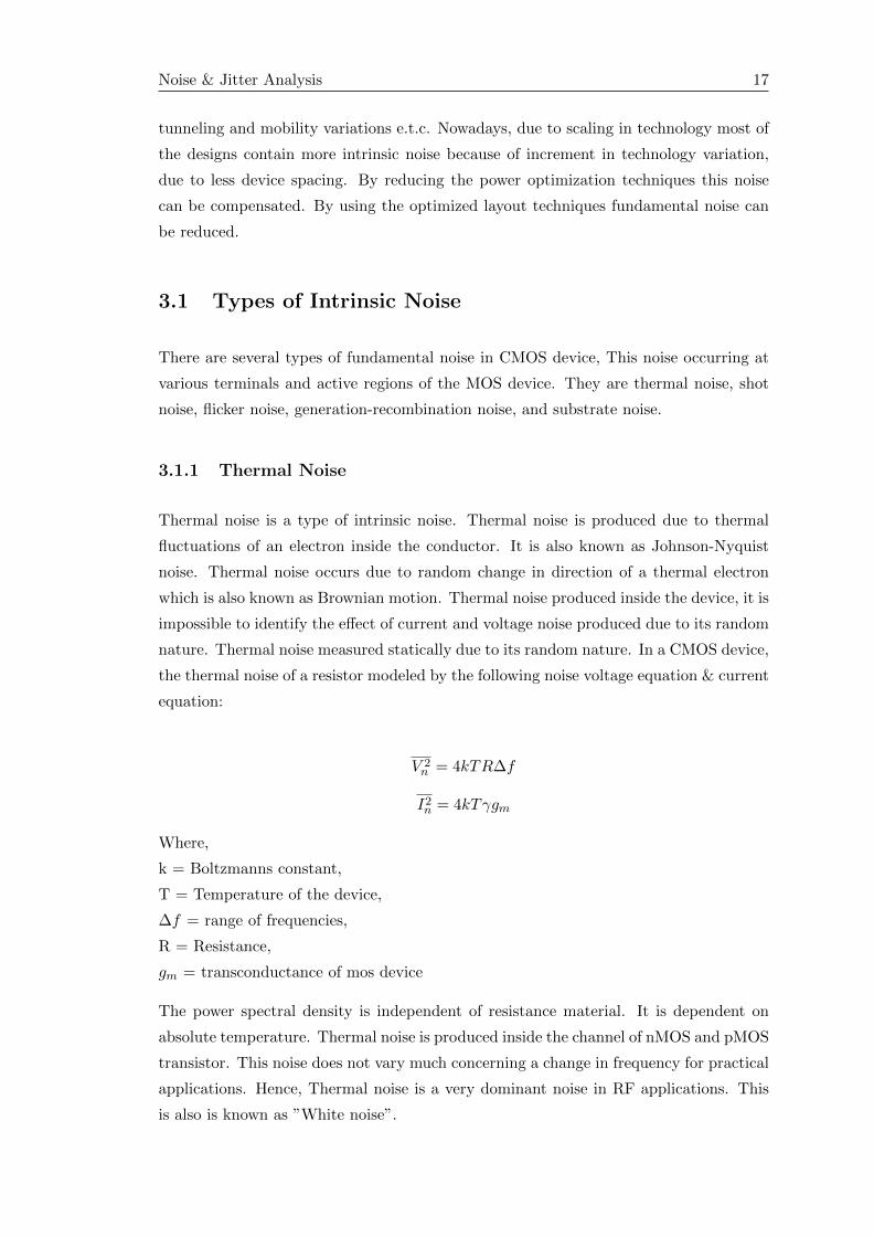
3.1.1 Thermal Noise
Thermal noise is a type of intrinsic noise. Thermal noise is produced due to thermal
fluctuations of an electron inside the conductor. It is also known as Johnson-Nyquist
noise. Thermal noise occurs due to random change in direction of a thermal electron
which is also known as Brownian motion. Thermal noise produced inside the device, it is
impossible to identify the effect of current and voltage noise produced due to its random
nature. Thermal noise measured statically due to its random nature. In a CMOS device,
the thermal noise of a resistor modeled by the following noise voltage equation & current
equation:
V 2n = 4kTR∆f
I2n = 4kTγgm
Where,
k = Boltzmanns constant,
T = Temperature of the device,
∆f = range of frequencies,
R = Resistance,
gm = transconductance of mos device
The power spectral density is independent of resistance material. It is dependent on
absolute temperature. Thermal noise is produced inside the channel of nMOS and pMOS
transistor. This noise does not vary much concerning a change in frequency for practical
applications. Hence, Thermal noise is a very dominant noise in RF applications. This
is also is known as ”White noise”.

Noise & Jitter Analysis 18
3.1.2 Shot Noise
When electrons and holes across the potential barrier in the transistor, This produces
the shot noise. These potential barriers are found at the junction depletion region,
channel depletion region in a CMOS device transistor. In the time domain, the current
is the sum of discrete pulses. The Current noise is proportional to temperature. Hence,
by lowering the temperature shot noise can be reduced.
3.1.3 Flicker Noise
Flicker noise is also called 1/f noise. Frequency is inversely proportional to the power
density of electronic devices. The main mechanism of flicker noise still under investi-
gation its exact mechanism and origination are uncertain and unknown. But, different
models suggest that it generates from the oxide traps which traps and release in the
channel. It has been suggested that it is generated from source, bulk, dangling bonds,
silicon interface. It has been found that for different devices, flicker noise has been
different.
Figure 3.1: corner frequency 1/f
Flicker noise has been generated from defects present at the surface and it can be modeled
easily, these defects depend on the fabrication of CMOS technology. Flicker noise is
lesser in PMOS than NMOS, because holes in PMOS keep the distance from these
traps. Flicker noise in CMOS devices can be modeled by a voltage source in series with
the gate or current source connected between drain and source. They are given by
V 2n =
K
WLCox
1
fm

Noise & Jitter Analysis 19
I2n = g2mK
WLCox
1
fm
Where,
W is the gate width,
L is the channel length,
Cox is the gate oxide capacitance per unit area,
K is a constant
Fig.3.1[9] shows the flicker noise & thermal noise at which power spectral density of
thermal frequency 1/f intercepts at fc is known as corner frequency. By equating the
flicker and thermal noise, corner frequency fc at 1/f can be calculated[7].
g2mK
WLCox
1
fm= 4kTγgm ⇔ fc =
K
WLCox
gm4kTγ
3.1.4 Generation − Recombination noise
The Generation-Recombination noise is generated due to fluctuations in free carriers
with random charge carriers in different energy bands. This will cause a fluctuation in
current flow. It represents a typical noise that depends on the carrier concentration of
semiconductors material. The generation-recombination noise in MOS devices originates
from bulk silicon defects. These defects create traps that capture or release carriers.
Recombination noise is caused by these trapping centers in the bulk of the device.
Generation recombination noise in MOS is usually much smaller than 1/f noise.
3.1.5 Substrate noise
The noise produced through the substrate of a transistor is known as substrate noise. In
between drain, source and substrate virtual capacitors formed between the bulk, drain
or sources region. These capacitors only affect the high frequency, a small current will
pass through the bulk of the mos device because at high-frequency capacitors act as
short and it allows this leakage current. Lower frequency does not have any effect on
these capacitors at lower frequency capacitors act as an open. The following equation
shows the substrate noise dependency on the frequency with resistance.
fmax =ft2
√routRs

Noise & Jitter Analysis 20
The substrate noise affects the output resistance and output conductance of the device.
Frequency increases the output resistance will also increases, which leads to more sub-
strate noise. Most dominating noise is thermal noise as it tends to affect the wide range
of frequencies.
3.2 Oscillator Noise
Oscillator oscillates at its fundamental frequency which is f0. It produces sinusoidal
frequency. While converting into the frequency domain, sinusoidal frequency converts
into two Dirac delta function centered at frequencies -f0 and f0. If the oscillator is
ideal, all the energy distribute over this frequency. Practically, the oscillator has some
amount of energy distribute or spread around the oscillation centered frequency, which
is known as phase noise. Phase noise is the combination of noise discussed in the above
subsection thermal, shot, flicker, generation- recombination and substrate noise and
extrinsic noise. Oscillator amplitude has a maximum and minimum limit at which it
oscillates. The amplitude of the oscillator is controlled by the non-linearity in the circuit.
The amplitude and loop gain of the oscillator is inversely proportional to each other. If
amplitude decrease, loop gain increases or amplitude increases, loop gain decreases. If
there is a change in the phase of the oscillator, then is no loop restoring force. Hence
phase noise became the critical aspect of an oscillator.
3.2.1 Phase Noise In Oscillator
Phase noise or jitter are two important parameters of an oscillator. They have a direct
impact on the performance of a system. Noise can corrupt a signal, it can change
the frequency spectrum & timing spectrum of the signal. Phase noise and jitter are
associated with the noise of an oscillator. Phase noise is defined as the fluctuation in
the frequency output of an oscillator. It is due to the random change in the phase of
an oscillator. At frequency domain, due to intrinsic and extrinsic noise, the phase at
the central frequency of an oscillator changes from its original phase to an unwanted
phase of an oscillator. The Phase noise of an ideal and practical oscillator has been
shown in Fig.3.2. Ideally, an oscillator output must be pure sinusoidal, it must be Dirac
delta in frequency domain represented as a vertical line at a single frequency. However,
in practice, due to the noise source inside an oscillator, the output of an oscillator
changes to its original position near its carrier frequency. The output of an ideal and
real oscillator mathematically expressed as follows:
• Output of an ideal oscillator: V0 = A0 sin(ω0t)
Noise & Jitter Analysis 21
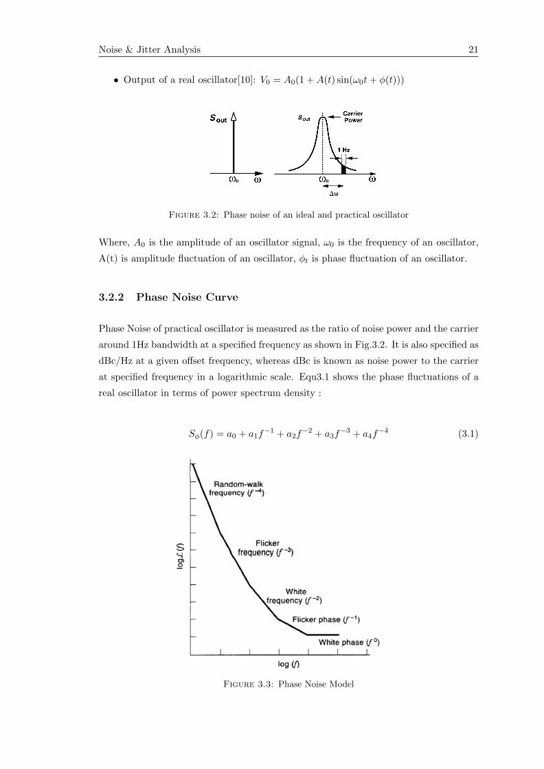
• Output of a real oscillator[10]: V0 = A0(1 +A(t) sin(ω0t+ φ(t)))
Figure 3.2: Phase noise of an ideal and practical oscillator
Where, A0 is the amplitude of an oscillator signal, ω0 is the frequency of an oscillator,
A(t) is amplitude fluctuation of an oscillator, φt is phase fluctuation of an oscillator.
3.2.2 Phase Noise Curve
Phase Noise of practical oscillator is measured as the ratio of noise power and the carrier
around 1Hz bandwidth at a specified frequency as shown in Fig.3.2. It is also specified as
dBc/Hz at a given offset frequency, whereas dBc is known as noise power to the carrier
at specified frequency in a logarithmic scale. Equ3.1 shows the phase fluctuations of a
real oscillator in terms of power spectrum density :
Sφ(f) = a0 + a1f−1 + a2f
−2 + a3f−3 + a4f
−4 (3.1)
Figure 3.3: Phase Noise Model

Noise & Jitter Analysis 22
The different components of noise have been defined by the coefficient of a & shown in
equ.3.1. The slope of the single-sideband phase noise, Lφ(f) is defined by the defined
spectrum degree frequency. As shown in Fig.3.3[11] spectrum degree with 0, -1, -2, -3,
-4 usually named as White phase modulation PM (WHPM), Flicker (FLPM), Random
Walk PM (RWPM) also known as White Frequency Modulation (WHIFM), Random
Run PM (RRPM or Flicker FM (FLFM)), and Random Walk (RWFM). Along with the
reduction of fm, a strong effect of the short-term noise of Lφ(f) appears. Closer the
frequency to the carrier, the larger Sφ(f) is. Extremely Sφ(f) will reach infinite. But
in the real circuits, it is not efficient that all components of Sφ(f) are presented. Each
component comes out only in the specific frequency range.
3.2.3 Leesons Phase Noise Model
The phase noise of an oscillator is described by an equation which is given by David B.
Leeson. Phase noise, Leeson model equation is given by[9]:
L(∆ω) = 10log
([2FkT
Psig
][1 +
( ω
2Q∆ω
)2][1 +
∆ω 1f3
∆ω
])dBc/Hz (3.2)
Where,
Psig = oscillator output power,
∆ω = offset from the oscillation frequency,
L(∆ω) = single sideband phase noise density,
F = active device noise factor,
∆ω1/f3 = break between 1/f flicker noise and a frequency range with slope 20 dB/decade.
Fig.3.4[9] shows Lesson phase noise model. Shot noise & thermal noise & dominates,
region between the ∆ω/2Q and ∆ω1/f3 . 1kHz region lies behind ∆ω1/f3 . ∆ω/2Q lies
around in the few MHz region. As shown above in lesson noise model equ.3.2, Phase
noise of an oscillator can be reduced:
• The power dissipated by the oscillator and quality factor of an oscillator is directly
proportional to the carrier to noise. To reduce the phase noise or noise around the
carrier, the quality factor of the oscillator should be increased.
• It can be reduced by increasing the width and length of the device. This will
reduce the flicker noise. If the devices used for the oscillators have less device
noise, the phase noise of an oscillator can be improved. If the noise floor can be

Noise & Jitter Analysis 23
Figure 3.4: Leeson’s Phase Noise Model
moved further due to less intrinsic noise, at lower offset frequency noise will get
improved.
• It can be reduced by reducing the current consumption of a signal. The power
of the signal reduced, due to reduced current consumption. This will reduce the
phase noise of an oscillator.
3.3 Timing Jitter in Oscillator
Jitter is defined as short-term variations of the significant instants of a signal from their
ideal positions in time and essentially describes how far the signal period has deviated
from its ideal value. Jitter is a variation in the zero-crossing times of a signal or a
variation in the period of the signal. Jitter is often defined as an RMS quantity. Jitter is
composed of two major components, one that is predictable and one that is random. The
predictable component of jitter is called deterministic jitter. The random component of
jitter is called random jitter. Random jitter comes from the random phase noise, while
deterministic jitter comes from the deterministic noise[11].
3.3.1 Random Jitter
Random Jitter is uncorrelated jitter and describes timing variations caused by less pre-
dictable influences. Random jitter is characterized by a Gaussian distribution and as-
sumed to be unbounded. It can be caused by many sources, such as thermal or other
physical, random processes. These sources include are shot noise, thermal noise, flicker
noise[10].

Noise & Jitter Analysis 24
3.3.2 Deterministic Jitter
Deterministic jitter is created by identifiable interference signals. It is always bounded
in amplitude, has Specific (not random) causes, and cannot be analyzed statistically.
It is caused by many sources such as crosstalk between adjacent signal traces, EMI
radiation on a sensitive signal path, Noise from power layers of a multi-layer substrate
and simultaneous switching of multiple gates to the same logic state.

Chapter 4
Proposed Architecture Design
This chapter discusses the proposed crystal oscillator design with the proposed transcon-
ductance stage along with all blocks. This crystal oscillator is designed to produce a
25MHz clock with low phase noise and fast startup.
4.1 Proposed System Architecture
Table.4.1 shows the specification required to design crystal oscillator. Fig.4.1 shows the
proposed functional block diagram. The crystal oscillator starts when digital logic starts
working. This logic starts the gm stage (current stage & stage 1-7). Now, gm stages
provide sufficient gain and current to crystal. As discussed above in subsection 3.1.9
that currently given to crystal must not exceed the drive level of crystal and minimum
current must provide, so that the crystal starts its functionality. Due to sufficient gain
and current, the crystal starts to resonate at its fundamental frequency. Oscillation
starts to build slowly, at a certain time interval at which stable oscillation achieved, also
Table 4.1: Specification
Technology TSMC 28nm
Supply 1 1.8V (1.6V to 2.0V)
Supply 2 0.9V (0.8V to 1.0V)
Crystal Frequency 25MHz
Output clock 0 to 0.9V
Load Capacitor 10pF
Drive Level ≤200µW
Startup Time ≤1ms
Phase Noise @1kHz ≥-120dBc/Hz
Phase Noise @1MHz ≥-150dBc/Hz
Jitter @≥1MHz 10ps
25

Proposed Architecture Design 26
Figure 4.1: Proposed Architecture of Crystal Oscillator

Proposed Architecture Design 27
called as startup time. These sinusoidal oscillations can be converted to a square wave
pulse by the use of CMOS buffer[12] and Schmitt trigger[13].
4.2 Digital Logic
Digital logic consists of a combination of NAND gates and level shifters shown in Fig.4.2.
Operation starts at an active mode when A1, A2, A3 and reset is at high logic 1. This
logic pass through the NAND gate which gives logic’0’ to the input of level shifter shown
in Fig.4.3. Due to positive feedback present in the level shifter. It converts the input
logic ’0’ to output Out port to logic’1’ & output Outb port to logic’0’. Which gives SB0,
SB1, SB2 go to logic 0, and S0, S1, S2 go to logic 1. Standby mode, when only A3 and
reset is at logic’1’ others at logic’0’. S2 and SB2 go to logic ’1’ & ’0’. S1,S0 and SB1,
SB0 go to logic ’0’ & ’1’ respectively.
Figure 4.2: Digital Logic
Figure 4.3: Level Shifter

Proposed Architecture Design 28
4.3 Related Gm Stage
There are many traditional gm stage circuits for crystal oscillator, which are widely
used in the industry for crystal oscillator. Some of them are discussed are here. In this
section, Some of the existing Gm stage techniques have been discussed.
4.3.1 Pierce Inverter Gm Stage
There are many traditional gm stage circuits for crystal oscillator, which are widely used
in the industry for crystal oscillator. Pierce-Gate oscillator (Inverter based crystal oscil-
lator) shown in Fig.4.4[14] is very popular as a topology that minimizes the tank loading
minimizing the crystal de-Qing and consumes less power compared to the other topolo-
gies, the configuration is not robust and stable with Process, Voltage and Temperature
variations (PVT).
Figure 4.4: Inverter Gm stage
Figure 4.5: Small signal model of Inverter Gm stage
Gain =VOUTVIN1
=−(GM1 +GM0)
Gds1 +Gds0, R0 =
1
(GdsM1 +GdsM0)
These can significantly degrade the Phase Noise (PN) and Power Supply Rejection Ratio
(PSRR) performance, as well as the output frequency stability, one of the most important
parameters when designing crystal oscillator. Moreover, if the Transconductance of

Proposed Architecture Design 29
the sustaining amplifier varies significantly with PVT, the oscillator could even fail to
oscillate.
4.3.2 Class AB Gm Stage
This configuration has more robust and stable with Process, Voltage and Temperature
variations (PVT) than an inverter-based crystal oscillator. Class AB gm Stage circuit
is shown in Fig.4.6 needs an extra biasing circuit to bias M2 which introduces extra
complexity.
Figure 4.6: Class AB Gm Stage
Figure 4.7: Small signal model of class AB Gm Stage
Small signal analysis results:
Gain =VOUTVIN1
=−(GM1 +GM0)
Gds1 +Gds0, R0 =
1
(GdsM1 +GdsM0)
The area of the overall circuit increases, due to extra biasing circuit addition in the
overall architecture. This extra biasing circuit consists of diode-connected NMOS and
PMOS, which has PVT variation. This architecture has better phase noise than the
inverter-based crystal oscillator. If, the power supply of both architectures is the same

Proposed Architecture Design 30
as voltage sinusoidal swing rail to rail of this architecture is less than the previous
architecture. Due to lower rail to rail swing, power consumption is lower than the
previous architecture. It has more startup time than the other previous architecture,
because of the extra capacitor attached to the crystal.
4.4 Proposed Gm Stage
To mitigate the above-stated limitations of the gm stage. Gm boosting loop has been
proposed which consist of current stage shown in Fig.4.8 and its gain stage shown in
Fig.4.9. A Combination of current and gain stage leads to increment in gain and ampli-
tude as compared to the inverter and class AB push-pull gm stage. This configuration
has more robust and stable with PVT variations than the other architectures. This
architecture does not need extra bias circuit. This architecture has a full rail to rail
swing. This architecture can track and control the current consumption at input and
output.
Figure 4.8: Proposed Gm Current stage architecture

Proposed Architecture Design 31
In the proposed Gm current stage, When SB goes to zero, R1 and diode-connected
PMOS (M5) passes the current, these currents divided into two parts NMOS (M5, M6).
So, whenever the current tries to go more into NMOS (M6) than other current tries to
pull it back to NMOS (M5). This operation leads to compensate for current consumption
so it has less effect on PVT variation.
Figure 4.9: Proposed Gm gain stage architecture
In the proposed Gm gain stage, current stage PMOS (M8) current mirrors to PMOS
(M1). This stable current flows into the NMOS (M0). Due to which, Common mode
maintains between PMOS (M1) & NMOS (M0). Hence, the duty cycle of this archi-
tectures is best. This gain stage gives the fast startup time because the gain of the
architecture depends on the multiplication of transconductance NMOS (M0) and resis-
tance of PMOS (M1) & NMOS (M0). The proposed Gm stage improves the phase Noise
& jitter of the oscillator.
Gain equation of the proposed Gm stage:
A = A0
[1− s
z
1 + sp
]
Small signal analysis and gain of the proposed Gm stage:

Proposed Architecture Design 32
A0 =VOUTVIN1
=−GM0
Gds1 +Gds0= −GM0R0
Gain Bandwidth equation derivation:
The impedance of Cgd and Cdb capacitors of the devices are very large compared to the
impedance offered by COUT
R0 =1
(GdsM1 +GdsM0), z =
−GM0
CgdM0 + CgdM1
C0 = (CgdM0 + CgdM1 + CdbM0 + CdbM1 + COUT )
p = − (GdsM1 +GdsM0)
(CgdM0 + CgdM1 + CdbM0 + CdbM1 + COUT )= − 1
R0C0' −(GdsM1 +GdsM0)
COUT
This is a single pole system because zero occurs at a very high frequency. Gain Band-
width Product(GB) and is given by
GB = A0 ∗ p = −GM0R0 ∗
(− 1
R0C0
)=−GM0
C0
Figure 4.10: Small signal model of proposed Gm stage architecture
4.5 Buffer Stage
There are many ways to convert the sinusoidal wave to a square wave. One of the easiest
ways is to use a CMOS buffer shown in Fig.4.11[15]. The CMOS buffer consists of two
back to back inverters. The size of the second inverter increases by 3x, 7x to drive
the buffer capability. Reduced power supply and sub-threshold voltage, these buffers
are more vulnerable to noise reduced power supply and noise robustness. Due to these

Proposed Architecture Design 33
supply variations and PVT variation occurs these buffer may not able to give a better
duty cycle. These variations lead to false stabilize output. To improve the output
stabilization, The Schmitt trigger can be used. Another way is to increase the length &
width of the transistor, which leads to an increase in the area.
Figure 4.11: Buffer Stage
4.6 Schmitt Trigger Stage
CMOS buffers are limited to supply variation and noise robustness, one of the ways to
improve is to use Schmitt trigger design shown in Fig.4.12[15]. These are the positive
feedback circuit in which loop gain of this circuit is greater than one. Because of the
feedback present in the circuit, it stabilizes the output logic and reduces sensitivity to
noises. The input of these circuit changes below/above a predefined threshold level, due
to feedback output logic holds its value and undesired noise not able to trigger a change
at the output. This Schmitt trigger design consists of an inverter (M2, M1) and two more
pairs of PMOS (M2, M5) & NMOS (M0, M5). These two pairs of NMOS and PMOS
are used to provide positive feedback at logic low & high. When Vin < V thnmos, Vout
= VDD, and M4 is in saturated and on, both M0 & M1 are off. When Vin > V thnmos,
M0 became on whereas M1 remains off due to the present feedback voltage at its drain
terminal. This feedback voltage depends on the dimensions of M0, M4 and V thnmos.
VFB = VDD − VTHN − (V ′IN − VTHN ) ∗√
(WN1 ∗ LN2)/(WN2 ∗ LN1)
where L and W are the corresponding transistors length and width. VFB improves
the SNM of the ST-INV since a higher VNOISE is now required for switching N0 on
(V ′IN = VTHN + VFB). Therefore, the high switching threshold becomes :

Proposed Architecture Design 34
V ′IN = VTHN + (VDD − VTHN ) ∗(1 +
√(WN1 ∗ LN2)/(WN2 ∗ LN1))−1
Assuming that N1 and N2 have the same dimensions, the high switching threshold is
(VDD + VTHN )/2. Similarly, in case of pMOS transistors, the ST-INV low switching
threshold is:
V ′IN = VDD − VTHP + (VDD + VTHP ) ∗(1 +
√(WP1 ∗ LP2)/(WP2 ∗ LP1))−1
Assuming that P1 and P2 have the same dimensions, the low ST-INV switching threshold
is improved to (VDD - VTHP )/2.
Figure 4.12: Schmitt Trigger
Chapter 5
Result and Discussion
This chapter presents the simulation results of the proposed crystal oscillator and transcon-
ductance stage. The circuits are implemented in Cadence Virtuoso TSMC 28nm CMOS
technology and simulations took place using the HSPICE & SPECTRE simulator. The
characterization has been done on basis of many variables such as outer supply voltage
variation from 0.8v to 1.0v, inner supply voltage variation from 1.6v to 2.0v, temperature
variation from -40C to 125C, resistance and capacitance variation up to (45%), MOS
parameters mismatch is taken up to 3 σ. Other variations could be due fabrication pro-
cess variation such as Vth and Cox variation. Simulations have been performed for cross
corners with variation in MOSFET intrinsic parameters, temperature, and resistance.
Process corners are used for simulations are Typical, Fast Fast(FF), Fast Slow(FS), Slow
Fast(SF) and Slow Slow(SS). A total of 45 corners is being used for the simulation of
the proposed crystal oscillator.
5.1 Dc Analysis
This section contains the Dc analysis of the proposed transconductance stage of the
crystal oscillator. Dc analysis shows the operating point of the circuit. In this case, the
Dc analysis shows the operating point of the gm stage. As input varies from 0 to 1.8v,
and supply varies from 1.6v to 2.0v, the output characteristic of the transconductance
stage works as an amplifier input region between 0.7v to 1.1v. This region is in the
linear region as we discussed earlier in chapter 3. The input region between 0v to 0.6v
gives full supply voltage at the output, the input region between 1.2v to 1.8v output
goes to ground voltage. While doing the dc analysis, it has been found one gm stage
producing 200µA current at a Typical corner. 30% gm stage current variation has been
35

Result and Discussion 36
found out at cross corners. At cross corners, all gm stages (30-35)% current variations
have been found out.
Figure 5.1: Dc Sweep
5.2 Open Loop Analysis
This section contains the open loop analysis of the proposed transconductance stage of
the crystal oscillator. Open loop analysis has been done by a loop break technique. In
Fig 5.1, disconnect the crystal, then a 0V voltage source is placed in series in the loop,
one pin of the voltage loop connected to the loop input, the other pin to output pin.
Open loop stability analysis has been presented by using the cadence spectre.
Fig.5.2, represents open loop analysis of proposed crystal oscillator gm stages at PVT
variations. When all 7 gain stages are connected then gain achieved at the typical
corner is 15.14dB at the frequency of 25MHz. The phase margin of the gm stages at the
typical corner is 94.4o at the frequency of 25MHz. Gain @25MHz varies from 19.17dB
to 11.7dB. Phase @25MHz varies from 101o to 94.4o. At the low power mode, when only
4 gm stages are connected. At PVT corners, Gain @25MHz from 15.1dB to 7.761dB.
At PVT corners, phase @25MHz from 87.81o to 97.56o.

Result and Discussion 37
Figure 5.2: Open Loop Stability Analysis
5.3 Closed loop Ac Analysis
This section contains the closed loop ac analysis of the proposed crystal oscillator. Closed
loop analysis has been done by maintaining the loop. When crystal connected with all
the gm stages. Ac signal has been applied between Xin and crystal, then stability
analysis has been performed. Fig.5.3 represents the closed loop analysis results when all
the gm stages connected to the crystal at PVT corners.
Figure 5.3: Closed Loop Ac Analysis
At the series resonant frequency, L1 and C1 cancel, impedance is determined by R1.
The second higher frequency is the parallel resonant frequency. At parallel resonance,
resistance is at a maximum. A typical corner gain @25MHz is 24.7dB, the total phase
Result and Discussion 38
is 174.7o. At PVT corners the closed loop gain has been varied from 27.3dB to 21.2dB.
At PVT corners the closed loop phase has been varied from 165o to 176o. At the low
power mode, when only 4 gm stages are connected. At PVT corners, Gain has @25MHz
from 24.9dB to 17.5dB. At PVT corners, phase @25MHz from 164o to 175o.
5.4 Transient Analysis
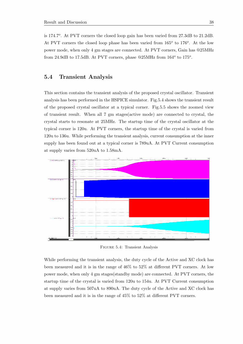
This section contains the transient analysis of the proposed crystal oscillator. Transient
analysis has been performed in the HSPICE simulator. Fig.5.4 shows the transient result
of the proposed crystal oscillator at a typical corner. Fig.5.5 shows the zoomed view
of transient result. When all 7 gm stages(active mode) are connected to crystal, the
crystal starts to resonate at 25MHz. The startup time of the crystal oscillator at the
typical corner is 120u. At PVT corners, the startup time of the crystal is varied from
120u to 136u. While performing the transient analysis, current consumption at the inner
supply has been found out at a typical corner is 789uA. At PVT Current consumption
at supply varies from 520uA to 1.58mA.
Figure 5.4: Transient Analysis
While performing the transient analysis, the duty cycle of the Active and XC clock has
been measured and it is in the range of 46% to 52% at different PVT corners. At low
power mode, when only 4 gm stages(standby mode) are connected. At PVT corners, the
startup time of the crystal is varied from 120u to 154u. At PVT Current consumption
at supply varies from 507uA to 890uA. The duty cycle of the Active and XC clock has
been measured and it is in the range of 45% to 52% at different PVT corners.

Result and Discussion 39
Figure 5.5: Close View of Transient Result
5.5 Phase Noise Analysis
This section contains the phase noise analysis on the proposed crystal oscillator. Fig.5.6
shows the phase noise result of the proposed crystal oscillator at XOUT, spectre simu-
lation has been used for phase noise simulation. Due to the novel loop technique phase
noise has been improved, lower the phase noise at different frequency better the noise im-
munity of crystal oscillator. Phase noise at 1Hz measured -49.711dBc/Hz, phase noise at
1KHz measured -136.67dBc/Hz, phase noise at 10kHz measured -148.21dBc/Hz, phase
noise at 10kHz measured -153.97dBc/Hz. 2% variations have been measured in phase
noise at different PVT corners.
Figure 5.6: Phase Noise
5.6 Jitter Analysis
This section contains the jitter analysis on the proposed crystal oscillator. Jitter analysis
has been done to check the variation due to overtone frequency(odd harmonics) on crystal
frequency. Fig.5.7 shows the jitter analysis result of the proposed crystal oscillator. Jitter

Result and Discussion 40
Figure 5.7: Jitter Analysis
is measured on the 1.8v power supply of crystal oscillator. A low pass filter has been
connected at the power supply to reject the frequency greater than 1MHz. As shown in
Fig.5.7 50mv of the sinusoidal pulse at different frequency starting from 100kHz, 1MHz,
12.5MHz, 37.5MHz, 62.5MHz, and 100MHz has been connected to the power supply.
It has been measured that maximum jitter variation on the 12.5MHz sinusoidal power
supply is 3ps. Overall jitter has measured from 1ps to 3ps at 100kHz, 1MHz, 12.5MHz,
37.5MHz, 62.5MHz, 100MHz sinusoidal frequency power supply.
5.7 Discussion
Table.5.1 shows the comparison of the performance metrics of the proposed crystal
oscillator with the other State-of-the-Art crystal oscillator available. The present work
has been noise efficient compared to the existing work. In the lowest technology node,
the best phase noise has been achieved, while comparing to an existing design. This
present work produced the best startup time at PVT corners compared to the existing
architecture. Most of the existing work has not mentioned or calculated the jitter for odd
harmonics of crystal. This work produced 3ps jitter which is the best till now. Most of
the existing work used the extra circuit to reduce the power which increases the area and
leads to more PVT variation. This work provides the best power consumption without
increasing the overall area with less PVT variation. The duty cycle has not measured
by the other state of the art. In this work, duty cycle has also been calculated. The
performance has been compared with [16] [12] [1] [13] [17] [18].

Result and Discussion 41
Table5.1:
Des
ign
Com
pari
son
wit
hex
isti
ng
des
ign
Tech
nolo
gy
28n
m(T
his
Wor
k)
65n
m[1
6]65
nm
[12]
65n
m[1
]40
nm
[13]
28n
m[1
7]90
nm
[18]
Su
pp
ly1.
8V1.
4V1.
8V3.
3V0.
7V1V
1.4
Osc
illa
tion
Fre
qu
en
cy
25M
Hz
38.4
MH
z26
MH
z39
.25M
Hz
39.2
5MH
z48
MH
z25
MH
z
Pow
er(µW
)14
2049
0014
4019
6915
0030
00
Sta
rtu
pT
imeµS
120
1250
3200
3900
259u
-25
00
Ph
ase
Nois
e@
1kH
z-1
37d
Bc/
Hz
-135
-136
-139
-120
-114
-140
Ph
ase
Nois
e@
1M
Hz
-154
dB
c/H
z-
--1
53-
-152
-152
Jit
ter
@≥
1M
Hz
3ps
--
--
--

Chapter 6
Conclusion
A novel low phase noise and fast startup time crystal oscillator has been implemented and
analyzed. This thesis discusses the design, circuit implementation and the performance
of the crystal oscillator to eliminate the existing design challenges. Initially, Various
types of oscillators have been discussed and addressed its limitations & why crystal
oscillator has been used. Due to more on-chip variations in this oscillator, the Crystal
oscillator’s advantages over the other oscillators are highlighted. Various parameters,
property’s and related work of crystal have been discussed. Noise and jitter analysis of
crystal oscillator has been discussed. The advantages of the proposed transconductance
stages of crystal oscillator have been discussed. This crystal oscillator is designed to
generate a reference clock for PLL, which requires less phase noise & fast startup time.
Drawbacks of crystal oscillators are highlighted and how the novel transconductance
technique overcomes the challenges shown in the thesis.
Simulation results of the crystal oscillator transconductance stage shows (30-35)% cur-
rent variations of gm stages, maximum & minimum current consumption at PVT corners
found out to be 1.58mA (when all the gm stages are on) and 362uA (when only four gm
stages are on) as a result at low power mode power consumption reduced. The imple-
mented transconductance stage shows 38% open loop Gain @25MHz & 22% closed loop
@25MHz variation at PVT corners. This technique leads to fast startup time which is
in the range from 120u to 154u. The duty cycle variation of the clock is in between (45%
- 52%). Phase noise improvement shown -136.67dBc/Hz at 1kHz and -148.21dBc/Hz at
10kHz. This technique leads to minimization in jitter which is in the range between 1ps
to 3ps.
The novel crystal oscillator design is developed in TSMC 28nm CMOS technology at
western digital, PVT variations have been discussed and presented thoroughly.
42

43
6.1 Future Work
In the current work, proposed crystal oscillator design and simulations performed at the
schematic level. As future work, post layout simulations can be done to verify the design
robustness against parasitic capacitance and resistances and more importantly off-chip
connection of crystal oscillator. The Power consumption of the current work can be
further improved by using the power management circuit.

Bibliography
[1] Shunta Iguchi Takayasu Sakurai Makoto Takamiya. A low-power cmos crystal oscil-
lator using a stacked-amplifier architecture. IEEE Journal Of Solid-State Circuits,
51(11):3006–3017, 2017.
[2] Shunta Iguchi Hiroshi Fuketa Takayasu Sakurai Makoto Takamiya. Variation-
tolerant quick-start-up cmos crystal oscillator with chirp injection and negative
resistance booster. IEEE Journal Of Solid-State Circuits, 51(2):496–508, 2016.
[3] Kannan Sankaragomathi Lori Callaghan Richard Ruby Brian Otis. A 220db fom,
1.9 ghz oscillator using a phase noise reduction technique for high-q oscillators. 2013
IEEE Radio Frequency Integrated Circuits Symposium (RFIC), 2013.
[4] Dongmin Yoon Taekwang Jang Dennis Sylvester David Blaauw. A 5.58 nw crystal
oscillator using pulsed driver for real-time clocks. IEEE Journal Of Solid-State
Circuits, 51(2):509–522, 2016.
[5] Statek. The quartz crystal model and its frequencies.
[6] Eric A. Vittoz Marc G. R. Degrauwe Serge Bitz. High-performance crystal oscillator
circuits: Theory and application. IEEE Journal Of Solid-State Circuits, 51(2):509–
522, 2016.
[7] Eric A. Vittoz. Low-Power Crystal and MEMS Oscillators.
[8] Kin Keung Lee Kristian Granhaug Nikolaj Andersen. A study of low-power crystal
oscillator design. 2013 NORCHIP Vilnius, Lithuania, 2013.
[9] Thomas H. Lee Ali Hajimiri. Oscillator phase noise: A tutorial. IEEE Journal Of
Solid-State Circuits, 35(3):326–336, 2000.
[10] Xianhe Huang Feng Tan Qilong Rong Wei Wei. Study and estimation of crystal
oscillator phase jitter. 2006 International Conference on Communications, Circuits
and Systems, 2007.
[11] David B. Leeson. Oscillator phase noise: A 50-year review. IEEE transactions on
ultrasonics, ferroelectrics, and frequency control, 63(8):1208–1225, 2016.
44

References 45
[12] Yuyu Chang John Leete Zhimin Zhou Morteza Vadipour Yin-Ting Chang and
Hooman Darabi. A differential digitally controlled crystal oscillator with a 14-
bit tuning resolution and sine wave outputs for cellular applications. IEEE Journal
Of Solid-State Circuits, 47(2):421–434, 2012.
[13] Shunta Iguchi Akira Saito Yunfei Zheng Kazunori Watanabe Takayasu Sakurai and
Makoto Takamiya. 93% power reduction by automatic self power gating (aspg)
and multistage inverter for negative resistance (minr) in 0.7v, 9.2uw, 39mhz crystal
oscillator. 2013 Symposium on VLSI Circuits Digest of Technical Papers, pages
10–4, 2013.
[14] Puneeth Kumar S. Rekha. Fast start crystal oscillator design with negative resis-
tance control. Integration, the VLSI Journal.
[15] Walid Ibrahim ; Valeriu Beiu ; Mihai Tache ; Fekri Kharbash. On schmitt trig-
ger and other inverters. 2013 IEEE 20th International Conference on Electronics,
Circuits, and Systems (ICECS), 2013.
[16] Danielle Griffith Fikret Dlger Gennady Feygin Ahmed Nader Mohieldin Prasanth
Vallur. A 65nm cmos dcxo system for generating 38.4mhz and a real time clock
from a single crystal in 0.09mm2. IEEE Radio Freq. Integr. Circuits Conf. Dig.
Tech. Papers, pages 321–324.
[17] Mohammad Mahdi Ghahramani Yashar Rajavi Alireza Khalili Amirpouya Kavou-
sian Beomsup Kim and Michael P. Flynn. A 192mhz differential xo based frequency
quadrupler with sub-picosecond jitter in 28nm cmos. 2015 IEEE Radio Frequency
Integrated Circuits Symposium (RFIC), 2015.
[18] Jerry (Heng-Chih) Lin. A low-phase-noise 0.004-ppm/step dcxo with guaranteed
monotonicity in the 90-nm cmos process. IEEE Journal Of Solid-State Circuits,
pages 2726–2734, 2005.
Recommended

![RFM110/RFM117€¦ · 1.4 Crystal Oscillator Table 6. Crystal Oscillator Specifications Parameter Symbol conditions min typ max unit Crystal Frequency[1] F XTAL 26 MHz Crystal Tolerance[2]](https://img.dokumen.tips/doc/110x75/5e7a7c857e3f1f22673379d8/rfm110rfm117-14-crystal-oscillator-table-6-crystal-oscillator-specifications.jpg)