LogiCORE IP 7 Series FPGAs TransceiversWizard v1.3 User Guide
UG769 (v1.0) March 1, 2011

7 Series FPGAs Transceivers Wizard User Guide www.xilinx.com UG769 (v1.0) March 1, 2011
Xilinx is providing this product documentation, hereinafter “Information,” to you “AS IS” with no warranty of any kind, express or implied. Xilinx makes no representation that the Information, or any particular implementation thereof, is free from any claims of infringement. You are responsible for obtaining any rights you may require for any implementation based on the Information. All specifications are subject to change without notice.
XILINX EXPRESSLY DISCLAIMS ANY WARRANTY WHATSOEVER WITH RESPECT TO THE ADEQUACY OF THE INFORMATION OR ANY IMPLEMENTATION BASED THEREON, INCLUDING BUT NOT LIMITED TO ANY WARRANTIES OR REPRESENTATIONS THAT THIS IMPLEMENTATION IS FREE FROM CLAIMS OF INFRINGEMENT AND ANY IMPLIED WARRANTIES OF MERCHANTABILITY OR FITNESS FOR A PARTICULAR PURPOSE.
Except as stated herein, none of the Information may be copied, reproduced, distributed, republished, downloaded, displayed, posted, or transmitted in any form or by any means including, but not limited to, electronic, mechanical, photocopying, recording, or otherwise, without the prior written consent of Xilinx.
© Copyright 2011. Xilinx, Inc. XILINX, the Xilinx logo, Artix, ISE, Kintex, Spartan, Virtex, and other designated brands included herein are trademarks of Xilinx in the United States and other countries. CPRI is a trademark of Siemens AG. PCI, PCI-SIG, PCI EXPRESS, PCIE, PCI-X, PCI HOT PLUG, MINI PCI, EXPRESSMODULE, and the PCI, PCI-X, PCI HOT PLUG, and MINI PC design marks are trademarks, registered trademarks, and/or service marks of PCI-SIG. All other trademarks are the property of their respective owners.
Revision HistoryThe following table shows the revision history for this document.
Date Version Revision
03/01/11 1.0 Initial Xilinx release.

Table of Contents
Revision History . . . . . . . . . . . . . . . . . . . . . . . . . . . . . . . . . . . . . . . . . . . . . . . . . . . . . . . . . . . . . 2
Preface: About This GuideGuide Contents . . . . . . . . . . . . . . . . . . . . . . . . . . . . . . . . . . . . . . . . . . . . . . . . . . . . . . . . . . . . . . 5Additional Resources . . . . . . . . . . . . . . . . . . . . . . . . . . . . . . . . . . . . . . . . . . . . . . . . . . . . . . . . 5
Chapter 1: IntroductionAbout the Wizard . . . . . . . . . . . . . . . . . . . . . . . . . . . . . . . . . . . . . . . . . . . . . . . . . . . . . . . . . . . . 7
Features . . . . . . . . . . . . . . . . . . . . . . . . . . . . . . . . . . . . . . . . . . . . . . . . . . . . . . . . . . . . . . . . . . 8Supported Devices . . . . . . . . . . . . . . . . . . . . . . . . . . . . . . . . . . . . . . . . . . . . . . . . . . . . . . . . . 8Provided with the Wizard . . . . . . . . . . . . . . . . . . . . . . . . . . . . . . . . . . . . . . . . . . . . . . . . . . 8
Recommended Design Experience . . . . . . . . . . . . . . . . . . . . . . . . . . . . . . . . . . . . . . . . . . . . 8Related Xilinx Documents . . . . . . . . . . . . . . . . . . . . . . . . . . . . . . . . . . . . . . . . . . . . . . . . . . . . 9Technical Support. . . . . . . . . . . . . . . . . . . . . . . . . . . . . . . . . . . . . . . . . . . . . . . . . . . . . . . . . . . . 9Ordering Information . . . . . . . . . . . . . . . . . . . . . . . . . . . . . . . . . . . . . . . . . . . . . . . . . . . . . . . . 9Feedback. . . . . . . . . . . . . . . . . . . . . . . . . . . . . . . . . . . . . . . . . . . . . . . . . . . . . . . . . . . . . . . . . . . . . 9
Transceiver Wizard . . . . . . . . . . . . . . . . . . . . . . . . . . . . . . . . . . . . . . . . . . . . . . . . . . . . . . . . 9Document . . . . . . . . . . . . . . . . . . . . . . . . . . . . . . . . . . . . . . . . . . . . . . . . . . . . . . . . . . . . . . . 10
Chapter 2: Installing the WizardTools and System Requirements. . . . . . . . . . . . . . . . . . . . . . . . . . . . . . . . . . . . . . . . . . . . . 11
Operating Systems . . . . . . . . . . . . . . . . . . . . . . . . . . . . . . . . . . . . . . . . . . . . . . . . . . . . . . . . 11Design Tools . . . . . . . . . . . . . . . . . . . . . . . . . . . . . . . . . . . . . . . . . . . . . . . . . . . . . . . . . . . . . 11
Before You Begin . . . . . . . . . . . . . . . . . . . . . . . . . . . . . . . . . . . . . . . . . . . . . . . . . . . . . . . . . . . 12Installing the Wizard . . . . . . . . . . . . . . . . . . . . . . . . . . . . . . . . . . . . . . . . . . . . . . . . . . . . . . . . 12Verifying Your Installation . . . . . . . . . . . . . . . . . . . . . . . . . . . . . . . . . . . . . . . . . . . . . . . . . . 12
Chapter 3: Running the WizardOverview . . . . . . . . . . . . . . . . . . . . . . . . . . . . . . . . . . . . . . . . . . . . . . . . . . . . . . . . . . . . . . . . . . . 15
Functional Overview . . . . . . . . . . . . . . . . . . . . . . . . . . . . . . . . . . . . . . . . . . . . . . . . . . . . . . 15Structure of the Example Design and Testbench . . . . . . . . . . . . . . . . . . . . . . . . . . . . . . 17Example Design – XAUI Configuration . . . . . . . . . . . . . . . . . . . . . . . . . . . . . . . . . . . . . . 18
Setting Up the Project . . . . . . . . . . . . . . . . . . . . . . . . . . . . . . . . . . . . . . . . . . . . . . . . . . . . . . . 19Creating a Directory . . . . . . . . . . . . . . . . . . . . . . . . . . . . . . . . . . . . . . . . . . . . . . . . . . . . . . 19Setting the Project Options . . . . . . . . . . . . . . . . . . . . . . . . . . . . . . . . . . . . . . . . . . . . . . . . . 20
Configuring and Generating the Wrapper . . . . . . . . . . . . . . . . . . . . . . . . . . . . . . . . . . . 21Line Rate, GT Placement, and Clocking . . . . . . . . . . . . . . . . . . . . . . . . . . . . . . . . . . . . . . 22Encoding and Optional Ports . . . . . . . . . . . . . . . . . . . . . . . . . . . . . . . . . . . . . . . . . . . . . . . 25Alignment, Termination, and Equalization . . . . . . . . . . . . . . . . . . . . . . . . . . . . . . . . . . . 30PCI Express, SATA, OOB, PRBS, Channel Bonding, and Clock Correction Selection 34Channel Bonding and Clock Correction Sequence . . . . . . . . . . . . . . . . . . . . . . . . . . . . . 38Summary . . . . . . . . . . . . . . . . . . . . . . . . . . . . . . . . . . . . . . . . . . . . . . . . . . . . . . . . . . . . . . . . 40
7 Series FPGAs Transceivers Wizard User Guide www.xilinx.com 3UG769 (v1.0) March 1, 2011

Chapter 4: Quick Start Example DesignOverview . . . . . . . . . . . . . . . . . . . . . . . . . . . . . . . . . . . . . . . . . . . . . . . . . . . . . . . . . . . . . . . . . . . 41Functional Simulation of the Example Design . . . . . . . . . . . . . . . . . . . . . . . . . . . . . . . 41
Using ModelSim . . . . . . . . . . . . . . . . . . . . . . . . . . . . . . . . . . . . . . . . . . . . . . . . . . . . . . . . . . 41Implementing the Example Design . . . . . . . . . . . . . . . . . . . . . . . . . . . . . . . . . . . . . . . . . . 42
Chapter 5: Detailed Example DesignDirectory and File Structure . . . . . . . . . . . . . . . . . . . . . . . . . . . . . . . . . . . . . . . . . . . . . . . . . 43Directory and File Contents . . . . . . . . . . . . . . . . . . . . . . . . . . . . . . . . . . . . . . . . . . . . . . . . . 44
<project directory> . . . . . . . . . . . . . . . . . . . . . . . . . . . . . . . . . . . . . . . . . . . . . . . . . . . . . . . 44<project directory>/<component name> . . . . . . . . . . . . . . . . . . . . . . . . . . . . . . . . . . . . 44<component name>/doc . . . . . . . . . . . . . . . . . . . . . . . . . . . . . . . . . . . . . . . . . . . . . . . . . . 45<component name>/example design . . . . . . . . . . . . . . . . . . . . . . . . . . . . . . . . . . . . . . . . 45<component name>/implement . . . . . . . . . . . . . . . . . . . . . . . . . . . . . . . . . . . . . . . . . . . . 46implement/results . . . . . . . . . . . . . . . . . . . . . . . . . . . . . . . . . . . . . . . . . . . . . . . . . . . . . . . . 46<component name>/simulation . . . . . . . . . . . . . . . . . . . . . . . . . . . . . . . . . . . . . . . . . . . . 46simulation/functional . . . . . . . . . . . . . . . . . . . . . . . . . . . . . . . . . . . . . . . . . . . . . . . . . . . . . 47
Example Design Description . . . . . . . . . . . . . . . . . . . . . . . . . . . . . . . . . . . . . . . . . . . . . . . . 48Example Design Hierarchy . . . . . . . . . . . . . . . . . . . . . . . . . . . . . . . . . . . . . . . . . . . . . . . . . . 49
4 www.xilinx.com 7 Series FPGAs Transceivers Wizard User GuideUG769 (v1.0) March 1, 2011

Preface
About This Guide
This guide describes the function and operation of the Xilinx® LogiCORE ™ IP 7 Series FPGAs Transceivers Wizard v1.3.
Guide ContentsThis guide contains the following chapters:
• Preface, About This Guide introduces the organization and purpose of this guide, a list of additional resources, and the conventions used in this document.
• Chapter 1, Introduction describes the Wizard and related information, including additional resources, technical support, and submitting feedback to Xilinx.
• Chapter 2, Installing the Wizard provides information about installing and licensing the Transceiver Wizard.
• Chapter 3, Running the Wizard provides an overview of the Transceiver Wizard, and a step-by-step tutorial to generate a sample transceiver wrapper with the Xilinx® CORE Generator™ tool.
• Chapter 4, Quick Start Example Design introduces the example design that is included with the transceiver wrappers. The example design demonstrates how to use the wrappers and demonstrates some of the key features of the transceiver.
• Chapter 5, Detailed Example Design provides detailed information about the example design, including a description of files and the directory structure generated by the CORE Generator tool, the purpose and contents of the provided scripts, the contents of the example HDL wrappers, and the operation of the demonstration testbench.
Additional ResourcesTo find additional documentation, see the Xilinx website at:
http://www.xilinx.com/support/documentation/index.htm.
To search the Answer Database of silicon, software, and IP questions and answers, or to create a technical support WebCase, see the Xilinx website at:
http://www.xilinx.com/support/mysupport.htm.
7 Series FPGAs Transceivers Wizard User Guide www.xilinx.com 5UG769 (v1.0) March 1, 2011

Preface: About This Guide
6 www.xilinx.com 7 Series FPGAs Transceivers Wizard User GuideUG769 (v1.0) March 1, 2011

Chapter 1
Introduction
This chapter introduces and describes the Xilinx® LogiCORE ™ IP 7 Series FPGAs Transceivers Wizard and provides related information, including additional resources, technical support, and instruction for submitting feedback to Xilinx.
About the WizardThe Transceiver Wizard automates the task of creating HDL wrappers to configure the high-speed serial transceivers in the Xilinx Virtex®-7 and Kintex™-7 FPGAs.
The Transceiver Wizard is a Xilinx® CORE Generator™ tool designed to support both Verilog and VHDL design environments. In addition, the example design delivered with the Wizard is provided in Verilog or VHDL.
The menu-driven interface allows one or more transceivers to be configured using pre-defined templates for popular industry standards, or from scratch, to support a wide variety of custom protocols. The Wizard produces a wrapper, an example design, and a testbench for rapid integration and verification of the serial interface with your custom function.
The Wizard produces a wrapper that instantiates one or more properly configured transceivers for custom applications (Figure 1-1).X-Ref Target - Figure 1-1
Figure 1-1: Transceiver Wizard Wrapper
ApplicationPorts
Customization Wrapper
GT
UG769_c1_01_122110
TransceiverPorts
ConfigParameters
(GigabitTransceiver)
7 Series FPGAs Transceivers Wizard User Guide www.xilinx.com 7UG769 (v1.0) March 1, 2011

Chapter 1: Introduction
The Transceiver Wizard can be accessed from the ISE® software CORE Generator tool. For information about system requirements and installation, see Chapter 2, Installing the Wizard.
For the latest information on this wizard, refer to the Xilinx Architecture Wizards product information page, located at http://www.xilinx.com/products/design_resources/conn_central/solution_kits/wizards/.
Features• Creates customized HDL wrappers to configure transceivers in the Virtex-7 and
Kintex-7 FPGAs
• The Wizard can configure transceivers in the Virtex-7 and Kintex-7 FPGAs to conform to industry standard protocols using predefined templates, or tailored for custom protocols
• Templates include support for the following specifications: 10GBASE-R, CPRI, Gigabit Ethernet, RXAUI, XAUI, and XLAUI
• Automatically configures transceiver analog settings of the PMA
• Each custom wrapper includes example design, testbench and simulation scripts
• Supports 64B/66B, 64B/67B, and 8B/10B encoding/decoding
Supported DevicesThe Wizard supports the Virtex-7 and Kintex-7 FPGAs.
For a complete listing of supported devices, see the Release Notes for this Wizard.
For more information on the 7 series devices, see the 7 Series FPGAs Overview.
Provided with the WizardThe following are provided with the Wizard:
Recommended Design ExperienceThe Transceiver Wizard is a fully verified solution that helps automate the task of defining parameter settings for 7 Series Xilinx® Multi-Gigabit Serial Transceivers. The additional challenge associated with implementing a complete design will vary depending on the configuration and required functionality of the application. Previous experience building high-performance, pipelined FPGA designs using Xilinx implementation software and user constraints files (UCF) is recommended.
• Documentation: This user guide
• Design Files: Verilog and VHDL
• Example Design: Verilog and VHDL
• Constraints File: Constraints file
• Testbench: Verilog and VHDL
• Simulation Model: Verilog and VHDL
8 www.xilinx.com 7 Series FPGAs Transceivers Wizard User GuideUG769 (v1.0) March 1, 2011
Related Xilinx Documents
For those with less experience, Xilinx offers various training classes to help you with various aspects of designing with Xilinx FPGAs. These include classes on such topics as designing for performance and designing with multi-gigabit serial I/O. For more information, see http://www.xilinx.com/training.
Your local Xilinx sales representative can provide a closer review and estimation for your specific requirements.
Related Xilinx DocumentsFor detailed information and updates about the Transceiver Wizard, see the following documents located at the Architecture Wizards page:
• UG769: LogiCORE IP 7 Series FPGAs Transceivers Wizard v1.3 User Guide
• Transceiver Wizard Release Notes
Prior to generating the Transceiver Wizard, users should be familiar with the following:
• DS180: 7 Series FPGAs Overview
• UG476: 7 Series FPGAs Transceivers User Guide
• ISE® software documentation: www.xilinx.com/ise
Technical SupportFor technical support, go to www.xilinx.com/support. Questions are routed to a team of engineers with expertise using the Transceiver Wizard.
Xilinx provides technical support for use of this product as described in this guide. Xilinx cannot guarantee timing, functionality, or support of this product for designs that do not follow these guidelines.
Ordering InformationThe Transceiver Wizard is provided free of charge under the terms of the Xilinx End User License Agreement. The Wizard can be generated by the Xilinx ISE CORE Generator software, which is a standard component of the Xilinx ISE Design Suite. This version of the Wizard can be generated using the ISE CORE Generator system v13.1. For more information, please visit the Architecture Wizards web page. Information about additional Xilinx LogiCORE modules is available at the Xilinx IP Center. For pricing and availability of other Xilinx LogiCORE modules and software, please contact your local Xilinx sales representative.
FeedbackXilinx welcomes comments and suggestions about the Transceiver Wizard and the accompanying documentation.
Transceiver WizardFor comments or suggestions about the Transceiver Wizard, please submit a WebCase from www.xilinx.com/support. (Registration is required to log in to WebCase.) Be sure to include the following information:
• Product name
7 Series FPGAs Transceivers Wizard User Guide www.xilinx.com 9UG769 (v1.0) March 1, 2011

Chapter 1: Introduction
• Wizard version number
• List of parameter settings
• Explanation of your comments, including whether the case is requesting an enhancement (you believe something could be improved) or reporting a defect (you believe something isn’t working correctly).
DocumentFor comments or suggestions about this document, please submit a WebCase from www.xilinx.com/support. (Registration is required to log in to WebCase.) Be sure to include the following information:
• Document title
• Document number
• Page number(s) to which your comments refer
• Explanation of your comments, including whether the case is requesting an enhancement (you believe something could be improved) or reporting a defect (you believe something isn’t documented correctly).
10 www.xilinx.com 7 Series FPGAs Transceivers Wizard User GuideUG769 (v1.0) March 1, 2011

Chapter 2
Installing the Wizard
This chapter provides instructions for installing the Xilinx® LogiCORE ™ IP 7 Series FPGAs Transceivers Wizard v1.3 in the Xilinx® CORE Generator™ tool.
Tools and System Requirements
Operating Systems
Windows
• Windows XP Professional 32-bit/64-bit
• Windows Vista Business 32-bit/64-bit
Linux
• Red Hat Enterprise Linux WS v4.0 32-bit/64-bit
• Red Hat Enterprise Desktop v5.0 32-bit/64-bit (with Workstation Option)
• SUSE Linux Enterprise (SLE) v10.1 32-bit/64-bit Design Tools
Design Tools
Design Entry
• CORE Generator software 13.1
Simulation
• ISE® software 13.1
• Mentor Graphics ModelSim 6.6d
• Cadence Incisive Enterprise (IES) 10.2
• Synopsys VCS and VCS MX 2010.06
Check the release notes for the required Service Pack; ISE Service Packs can be downloaded from www.xilinx.com/support/download.htm.
Synthesis
• XST 13.1
7 Series FPGAs Transceivers Wizard User Guide www.xilinx.com 11UG769 (v1.0) March 1, 2011

Chapter 2: Installing the Wizard
Before You BeginBefore installing the Wizard, you must have a MySupport account and the ISE 13.1 software installed on your system. If you already have an account and have the software installed, go to Installing the Wizard, otherwise do the following:
1. Click Login at the top of the Xilinx home page then follow the onscreen instructions to create a MySupport account.
2. Install the ISE 13.1 software.
For the software installation instructions, see the ISE Design Suite Release Notes and Installation Guide available in ISE software Documentation.
Installing the WizardThe Transceiver Wizard is included with the ISE 13.1 software. Follow the ISE 13.1 installation instructions in the ISE Installation and Release Notes available in www.xilinx.com/support/documentation under the "Design Tools" tab.
Verifying Your InstallationUse the following procedure to verify that you have successfully installed the Transceiver Wizard in the CORE Generator tool.
1. Start the CORE Generator tool.
2. The IP core functional categories appear at the left side of the window (Figure 2-1).
3. Click to expand or collapse the view of individual functional categories, or click the View by Name tab at the top of the list to see an alphabetical list of all cores in all categories.
X-Ref Target - Figure 2-1
Figure 2-1: CORE Generator Window
UG769_c2_01_122110
12 www.xilinx.com 7 Series FPGAs Transceivers Wizard User GuideUG769 (v1.0) March 1, 2011

Verifying Your Installation
4. Determine if the installation was successful by verifying that Transceiver Wizard 1.3 appears at the following location in the Functional Categories list:/FPGA Features and Design/IO Interfaces
7 Series FPGAs Transceivers Wizard User Guide www.xilinx.com 13UG769 (v1.0) March 1, 2011

Chapter 2: Installing the Wizard
14 www.xilinx.com 7 Series FPGAs Transceivers Wizard User GuideUG769 (v1.0) March 1, 2011

Chapter 3
Running the Wizard
OverviewThis chapter provides a step-by-step procedure for generating a transceiver wrapper, implementing the wrapper in hardware using the accompanying example design, and simulating the wrapper with the provided example testbench.
Note: The screen captures in this chapter are conceptual representatives of their subjects and provide general information only. For the latest information, see the Xilinx ® CORE Generator™ tool.
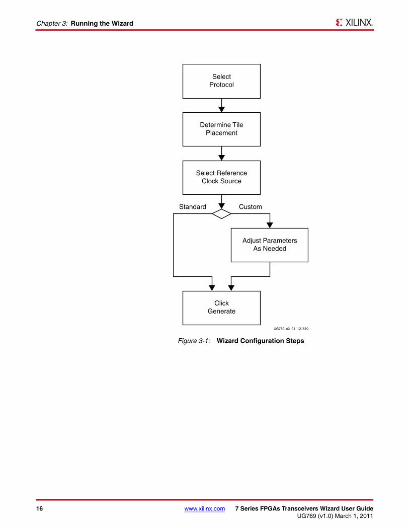
Functional OverviewFigure 3-1, page 16 shows the steps required to configure transceivers using the Wizard. Start the CORE Generator ™ software and select the Transceiver Wizard, then follow the chart to configure the transceivers and generate a wrapper that includes the accompanying example design.
• If you use an existing template with no changes, click Generate.
• If you are modifying a standard template or starting from scratch, proceed through the Wizard and adjust the settings as needed.
See Configuring and Generating the Wrapper, page 21 for details on the various transceiver features and parameters available.
7 Series FPGAs Transceivers Wizard User Guide www.xilinx.com 15UG769 (v1.0) March 1, 2011
Chapter 3: Running the Wizard
X-Ref Target - Figure 3-1
Figure 3-1: Wizard Configuration Steps
UG769_c3_01_121610
Determine TilePlacement
Select ReferenceClock Source
SelectProtocol
ClickGenerate
Adjust ParametersAs Needed
Standard Custom
16 www.xilinx.com 7 Series FPGAs Transceivers Wizard User GuideUG769 (v1.0) March 1, 2011

Overview
Structure of the Example Design and TestbenchFigure 3-2 illustrates the structure of the example design and testbench files generated with the GT wrapper. For details, see Example Design Description, page 48.
The following files are provided to demonstrate how to simulate the configured transceiver:
• GT Wrapper, which includes:
• The specific gigabit transceiver configuration parameters set using the Wizard.
• Transceiver primitive(s) selected using the Wizard.
• Example Design illustrating modules required to simulate the wrapper. The components are:
• FRAME_GEN Module: Generates a user-definable data stream for simulation analysis.
• FRAME_CHECK Module: Tests for correct transmission of data stream for simulation analysis.
• Tx Data File: Specifies the data pattern to be transmitted to transceiver.
• Rx Data File: Specifies the data pattern that should be compared against receive data from transceiver.
• GT_USRCLK_SOURCE Module: Generates required clock signals for GT transceiver.
• Testbench: Top-level testbench demonstrating how to stimulate the design.
X-Ref Target - Figure 3-2
Figure 3-2: Structure of the Example Design and Testbench
Example Design
Configuration Parameters
Testbench
FRAME_GEN
FRAME_CHECKRx Data File
Tx Data File
GT_USRCLK_SOURCEMODULE
Transceivers
Wrapper
UG769_c3_02_010911
7 Series FPGAs Transceivers Wizard User Guide www.xilinx.com 17UG769 (v1.0) March 1, 2011

Chapter 3: Running the Wizard
Example Design – XAUI ConfigurationThe example design covered in this section is a wrapper that configures a group of GT transceivers for use in a XAUI application. Guidelines are also given for incorporating the wrapper in a design and for the expected behavior in operation. For detailed information, see Chapter 4, Quick Start Example Design.
The XAUI example consists of the following components:
• A single transceiver wrapper implementing a four-lane XAUI port using four transceivers
• A demonstration testbench to drive the example design in simulation
• An example design providing clock signals and connecting an instance of the XAUI wrapper
The Transceiver Wizard example design has been tested with ModelSim 6.6d for simulation.
Figure 3-3 shows a block diagram of the default XAUI example design.X-Ref Target - Figure 3-3
Figure 3-3: XAUI Transceiver Configuration Example Design and Testbench
XAUI ConfigParameters
TransceiverPorts
Example Design
Transceiver(s)
UG769_c3_03_121610
XAUI Wrapper
Testbench
18 www.xilinx.com 7 Series FPGAs Transceivers Wizard User GuideUG769 (v1.0) March 1, 2011
Setting Up the Project
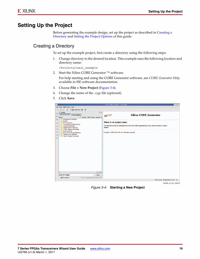
Setting Up the ProjectBefore generating the example design, set up the project as described in Creating a Directory and Setting the Project Options of this guide.
Creating a DirectoryTo set up the example project, first create a directory using the following steps:
1. Change directory to the desired location. This example uses the following location and directory name:
/Projects/xaui_example
2. Start the Xilinx CORE Generator ™ software.
For help starting and using the CORE Generator software, see CORE Generator Help, available in ISE software documentation.
3. Choose File > New Project (Figure 3-4).
4. Change the name of the .cgp file (optional).
5. Click Save. X-Ref Target - Figure 3-4
Figure 3-4: Starting a New ProjectUG769_c3_04_122010
7 Series FPGAs Transceivers Wizard User Guide www.xilinx.com 19UG769 (v1.0) March 1, 2011

Chapter 3: Running the Wizard
Setting the Project OptionsSet the project options using the following steps:
1. Click Part in the option tree.
2. Select Virtex7 from the Family list.
3. Select a device from the Device list that supports transceivers.
4. Select an appropriate package from the Package list. This example uses the XC7V1500T device (see Figure 3-5).
Note: If an unsupported silicon family is selected, the Transceiver Wizard remains light grey in the taxonomy tree and cannot be customized. Only devices containing transceivers are supported by the Wizard.
5. Click Generation in the option tree and select either Verilog or VHDL as the output language.
6. Click OK.
Note: Help opens the Xilinx ISE Help window.
X-Ref Target - Figure 3-5
Figure 3-5: Target Architecture SettingUG769_c3_05_122010
20 www.xilinx.com 7 Series FPGAs Transceivers Wizard User GuideUG769 (v1.0) March 1, 2011
Configuring and Generating the Wrapper
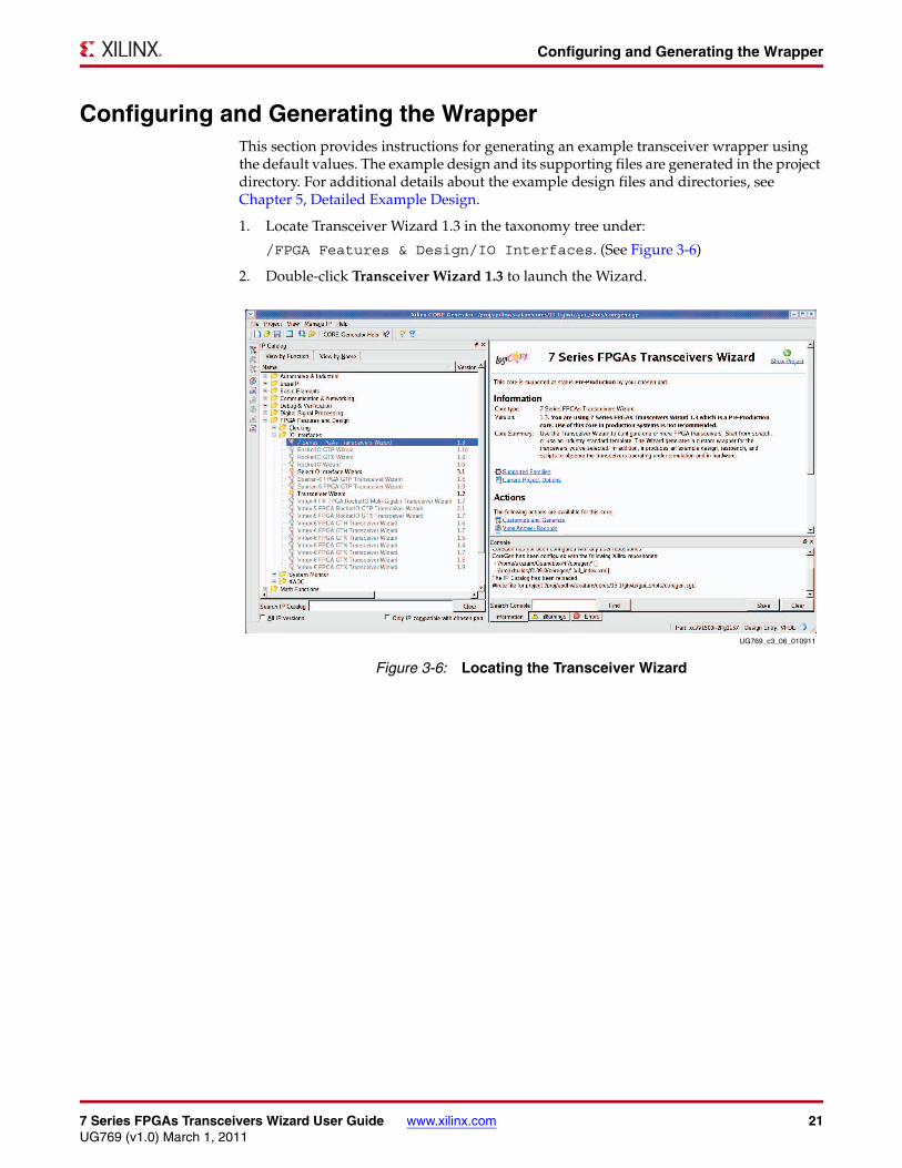
Configuring and Generating the WrapperThis section provides instructions for generating an example transceiver wrapper using the default values. The example design and its supporting files are generated in the project directory. For additional details about the example design files and directories, see Chapter 5, Detailed Example Design.
1. Locate Transceiver Wizard 1.3 in the taxonomy tree under:
/FPGA Features & Design/IO Interfaces. (See Figure 3-6)
2. Double-click Transceiver Wizard 1.3 to launch the Wizard.X-Ref Target - Figure 3-6
Figure 3-6: Locating the Transceiver Wizard
UG769_c3_06_010911
7 Series FPGAs Transceivers Wizard User Guide www.xilinx.com 21UG769 (v1.0) March 1, 2011

Chapter 3: Running the Wizard
Line Rate, GT Placement, and ClockingPage 1 of the Wizard (Figure 3-7) allows you to select the component name and determine the line rate, reference clock frequency, GT placement and clocking. In addition, this page specifies a protocol template.
The number of available transceivers appearing on this page depends on the selected target device and package. The XAUI example design uses four transceivers.
1. In the Component Name field, enter a name for the Wizard instance. This example uses the name xaui_wrapper.
2. From the Protocol Template list, select Start from scratch if you wish to manually set all parameters.
Select one of the available protocols from the list to begin your design with a pre-defined protocol template. The XAUI example uses the XAUI protocol template.
3. Use Tables 3-1 through 3-5 to determine the line rate, reference clock, and optional ports settings available on this page.
X-Ref Target - Figure 3-7
Figure 3-7: Line Rates, GT Selection and Clocking - Page 1
UG769_c3_07_010911
22 www.xilinx.com 7 Series FPGAs Transceivers Wizard User GuideUG769 (v1.0) March 1, 2011

Configuring and Generating the Wrapper
Table 3-1: TX Settings
Options Description
Line RateSet to the desired target line rate in Gb/s. Can be independent of the receive line rate.
The XAUI example uses 3.125 Gb/s.
Reference ClockSelect from the list the optimal reference clock frequency to be provided by the application.
The XAUI example uses 156.25 MHz.
TX offSelecting this option disables the TX path of the GT. The transceiver will act as a receiver only.
The XAUI example design requires both TX and RX functionality.
Notes: Options not used by the XAUI example are shaded.
Table 3-2: RX Settings
Options Description
Line RateSet to the desired target line rate in Gb/s.
The XAUI example uses 3.125 Gb/s.
Reference ClockSelect from the list the optimal reference clock frequency to be provided by the application.
The XAUI example uses 156.25 MHz.
RX offSelecting this option disables the RX path of the GT. The transceiver will act as a transmitter only.
The XAUI example design requires both TX and RX functionality.
Notes: Options not used by the XAUI example are shaded.
Table 3-3: Additional Options
Option Description
Use Common DRP Select this option to have the dynamic reconfiguration port signals of the COMMON block available to the application.
QUAD PLL Use the Quad PLL when all four transceivers of quad are used to save power. Quad PLL is shared across four transceivers of a quad.
Advanced Clocking OptionUse this check box to bring out all possible reference clock ports to the generated wrapper. Used for dynamic clock switching.
7 Series FPGAs Transceivers Wizard User Guide www.xilinx.com 23UG769 (v1.0) March 1, 2011

Chapter 3: Running the Wizard
Table 3-4: Select Transceiver and Reference Clocks
Option Description
GTSelect the individual GT transceivers by location to be used in the target design. The XAUI example requires four transceivers.
TX Clock Source Determines the source for the reference clock signal provided to each selected GT transceiver (see Table 3-5). Two differential clock signal input pin pairs, labeled REFCLK0 and REFCLK1 are provided for every four transceivers. The groups are labelled Q0 through Q4 starting at the bottom of the transceiver column. Each transceiver has access to the local signal group and one or two adjacent groups depending upon the transceiver position. The XAUI example uses the REFCLK0 signal from the group local to the four selected GT transceivers (REFCLK0 Q0 option).
RX Clock Source
Table 3-5: Reference Clock Source Options
Option Description
REFCLK0/1 Q0 GT reference clock local to transceivers Y0-Y3
REFCLK0/1 Q1 GT reference clock local to transceivers Y4-Y7
REFCLK0/1 Q2 GT reference clock local to transceivers Y8-Y11
REFCLK0/1 Q4 GT reference clock local to transceivers Y12-Y15
REFCLK0/1 Q5 GT reference clock local to transceivers Y16-Y19
REFCLK0/1 Q6 GT reference clock local to transceivers Y20-Y23
REFCLK0/1 Q7 GT reference clock local to transceivers Y24-Y27
REFCLK0/1 Q8 GT reference clock local to transceivers Y28-Y31
REFCLK0/1 Q9 GT reference clock local to transceivers Y32-Y35
GREFCLK Reference clock driven by internal fabric. Lowest performance option.
24 www.xilinx.com 7 Series FPGAs Transceivers Wizard User GuideUG769 (v1.0) March 1, 2011

Configuring and Generating the Wrapper
Encoding and Optional PortsPage 2 of the Wizard (Figure 3-8) allows you to select encoding and 8B/10B optional ports. Tables 3-6 through 3-12 list the available options.X-Ref Target - Figure 3-8
Figure 3-8: Encoding and Optional Ports - Page 2
UG769_c3_08_010911
7 Series FPGAs Transceivers Wizard User Guide www.xilinx.com 25UG769 (v1.0) March 1, 2011

Chapter 3: Running the Wizard
Table 3-6: TX Settings
Options Description
External Data Width
16Sets both the internal transmitter data path width and the transmitter application interface data width to two 8-bit bytes.
20
Sets the internal transmitter data path width to two 10-bit bytes (20-bits). If 8B/10B encoding is selected, the transmitter application interface data path width will be set to 16-bits. If 8B/10B encoding is not selected, the transmitter application interface data path width will be set to 20-bits.
32
Sets both the internal transmitter data path and the transmitter application interface data path width to four 8-bit bytes (32 bits) if internal data width is selected as 32 bits. For internal data width 16, transmitter data path width is 32 bits and internal data path width is 16
40
Sets the internal transmitter data path width to four 10-bit bytes (40 bits) if internal width is selected as 32 bits. If 8B/10B encoding is selected, the transmitter application interface data path width will be set to four 8-bit bytes (32 bits). If 8B/10B encoding is not selected, the transmitter application interface data path width will also be set.
64 Sets the internal transmitter data path width to four 8-bit bytes (32 bits). Sets the transmitter application interface data path width to eight 8-bit bytes (64 bits).
80
Sets the internal transmitter data path width to four 10-bit bytes (40 bits). If 8B/10B encoding is selected, the transmitter application interface data path width will be set to eight 8-bit bytes (64 bits). If 8B/10B encoding is not selected, the transmitter application interface data path width will be set to eight 10-bit bytes (80 bits).
Encoding
8B/10B Data stream is passed to an internal 8B/10B encoder prior to transmission.
64B/66B_with_Ext_Seq_Ctr
Data stream is passed through the 64B/66B gear-box and scrambler. Sequence counter for the gear-box is implemented in fabric
64B/66B_with_Int_Seq_Ctr
Data stream is passed through the 64B/66B gear-box and scrambler. Sequence counter for the gear-box is implemented within GT
64B/67B_with_Ext_Seq_Ctr
Data stream is passed through the 64B/67B gear-box and scrambler. Sequence counter for the gear-box is implemented in fabric
64B/67B_with_Int_Seq_Ctr
Data stream is passed through the 64B/67B gear-box and scrambler. Sequence counter for the gear-box is implemented within GT
Internal Data Width
16 Selects the internal data width as 16.
20 Selects the internal data width as 20.
32 Selects the internal data width as 32.
40 Selects the internal data width as 40.
Notes: Options not used by the XAUI example are shaded.
26 www.xilinx.com 7 Series FPGAs Transceivers Wizard User GuideUG769 (v1.0) March 1, 2011
Configuring and Generating the Wrapper
The TX PCS/PMA Phase Alignment setting controls whether the TX buffer is enabled or bypassed. See the 7 Series FPGAs Transceivers User Guide for details on this setting. The RX PCS/PMA Alignment setting controls whether the RX phase alignment circuit is enabled.
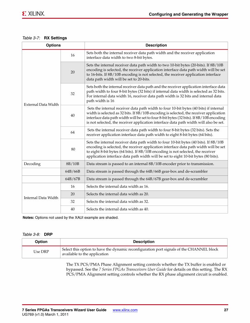
Table 3-7: RX Settings
Options Description
External Data Width
16Sets both the internal receiver data path width and the receiver application interface data width to two 8-bit bytes.
20
Sets the internal receiver data path width to two 10-bit bytes (20-bits). If 8B/10B encoding is selected, the receiver application interface data path width will be set to 16-bits. If 8B/10B encoding is not selected, the receiver application interface data path width will be set to 20-bits.
32
Sets both the internal receiver data path and the receiver application interface data path width to four 8-bit bytes (32 bits) if internal data width is selected as 32 bits. For internal data width 16, receiver data path width is 32 bits and internal data path width is 16
40
Sets the internal receiver data path width to four 10-bit bytes (40 bits) if internal width is selected as 32 bits. If 8B/10B encoding is selected, the receiver application interface data path width will be set to four 8-bit bytes (32 bits). If 8B/10B encoding is not selected, the receiver application interface data path width will also be set.
64 Sets the internal receiver data path width to four 8-bit bytes (32 bits). Sets the receiver application interface data path width to eight 8-bit bytes (64 bits).
80
Sets the internal receiver data path width to four 10-bit bytes (40 bits). If 8B/10B encoding is selected, the receiver application interface data path width will be set to eight 8-bit bytes (64 bits). If 8B/10B encoding is not selected, the receiver application interface data path width will be set to eight 10-bit bytes (80 bits).
Decoding 8B/10B Data stream is passed to an internal 8B/10B encoder prior to transmission.
64B/66B Data stream is passed through the 64B/66B gear-box and de-scrambler
64B/67B Data stream is passed through the 64B/67B gear-box and de-scrambler
Internal Data Width
16 Selects the internal data width as 16.
20 Selects the internal data width as 20.
32 Selects the internal data width as 32.
40 Selects the internal data width as 40.
Notes: Options not used by the XAUI example are shaded.
Table 3-8: DRP
Option Description
Use DRPSelect this option to have the dynamic reconfiguration port signals of the CHANNEL block available to the application
7 Series FPGAs Transceivers Wizard User Guide www.xilinx.com 27UG769 (v1.0) March 1, 2011

Chapter 3: Running the Wizard
Table 3-9 shows the optional ports for 8B/10B.
Table 3-10 details the TXUSRCLK and RXUSRCLK source signal options.
Table 3-11 details the TXOUTCLK and RXOUTCLK source signal options.
Table 3-9: 8B/10B Optional Ports
Option Description
TX
TXBYPASS8B10BTwo-bit wide port disables 8B/10B encoder on a per-byte basis. High-order bit affects high-order byte of data path.
TXCHARDISPMODE Two-bit wide ports control disparity of outgoing 8B/10B data. High-order bit affects high-order byte of data path.TXCHARDISPVAL
RX
RXCHARISCOMMATwo-bit wide port flags valid 8B/10B comma characters as they are encountered. High-order bit corresponds to high-order byte of data path.
RXCHARISKTwo-bit wide port flags valid 8B/10B K characters as they are encountered. High-order bit corresponds to high-order byte of data path.
Notes: Options not used by the XAUI example are shaded.
Table 3-10: TXUSRCLK and RXUSRCLK Source
Option Description
TX TXOUTCLK TXUSRCLK is driven by TXOUTCLK.
RX TXOUTCLKRXUSRCLK is driven by TXOUTCLK. This option is not available if the RX buffer is bypassed. For RX buffer bypass mode, RXOUTCLK is used to source RXUSRCLK
Table 3-11: TXOUTCLK and RXOUTCLK Source
Option Description
TXUse TXPLLREFCLK
If the check box Use TXPLLREFCLK is checked, TXOUTCLK(1) is generated from the input reference clock, else, the wizard selects the appropriate source for TXOUTCLK.
RXUse RXPLLREFCLK
If the check box Use RXPLLREFCLK is checked, RXOUTCLK(1) is generated from the input reference clock, else, the wizard selects the appropriate source for RXOUTCLK.
1. See the 7 Series FPGAs Transceivers User Guide for more information on TXOUTCLK and RXOUTCLK control.
28 www.xilinx.com 7 Series FPGAs Transceivers Wizard User GuideUG769 (v1.0) March 1, 2011

Configuring and Generating the Wrapper
Table 3-12 shows the optional ports available for latency and clocking.
Table 3-12: Optional Ports
Option Description
TXPCSRESET Active-High reset signal for the transmitter PCS logic.
TXBUFSTATUSTwo-bit signal monitors the status of the TX elastic buffer. This option is not available when the TX buffer is bypassed.
TXRATE Transmit rate change port
RXPCSRESET Active-High reset signal for the receiver PCS logic.
RXBUFSTATUS Indicates condition of the RX elastic buffer. Option is not available when the RX buffer is bypassed.
RXBUFRESETActive-High reset signal for the RX elastic buffer logic. This option is not available when the RX buffer is bypassed.
RXRATE Receive rate change port.
Notes: Options not used by the XAUI example are shaded.
7 Series FPGAs Transceivers Wizard User Guide www.xilinx.com 29UG769 (v1.0) March 1, 2011

Chapter 3: Running the Wizard
Alignment, Termination, and EqualizationPage 3 of the Wizard (Figure 3-9) allows you to set comma characters and control receive equalization and terminal voltage. X-Ref Target - Figure 3-9
Figure 3-9: Synchronization and Alignment - Page 3
UG769_c3_09_010911
30 www.xilinx.com 7 Series FPGAs Transceivers Wizard User GuideUG769 (v1.0) March 1, 2011

Configuring and Generating the Wrapper
Table 3-13 shows the settings for receive comma alignment.
Table 3-13: Comma Detection
Option Description
Use Comma DetectionEnables receive comma detection. Used to identify comma characters and SONET framing characters in the data stream.
Decode Valid Comma OnlyWhen receive comma detection is enabled, limits the detection to specific defined comma characters.
Comma ValueSelect one of the standard comma patterns or User Defined to enter a custom pattern. The XAUI example uses K28.5.
Plus Comma10-bit binary pattern representing the positive-disparity comma character to match. The right-most bit of the pattern is the first bit to arrive serially.
The XAUI example uses 0101111100 (K28.5).
Minus Comma10-bit binary pattern representing the negative-disparity comma character to match. The right-most bit of the pattern is the first bit to arrive serially.
The XAUI example uses 1010000011. (K28.5)
Comma Mask
10-bit binary pattern representing the mask for the comma match patterns. A 1 bit indicates the corresponding bit in the comma patterns is to be matched. A 0 bit indicates don’t care for the corresponding bit in the comma patterns.
The XAUI example matches the lower seven bits (K28.5).
Align to...
Any Byte Boundary When a comma is detected, the data stream is aligned using the comma pattern to the nearest byte boundary.
Two Byte Boundary When a comma is detected, the data stream is aligned using the comma pattern to the 2-byte boundary.
Four Byte Boundary When a comma is detected, the data stream is aligned using the comma pattern to the 4-byte boundary
Optional Ports
ENPCOMMAALIGN Active-High signal which enables the byte boundary alignment process when the plus comma pattern is detected.
ENMCOMMAALIGN Active-High signal which enables the byte boundary alignment process when the minus comma pattern is detected.
RXSLIDE Active-High signal that causes the byte alignment to be adjusted by one bit with each assertion. Takes precedence over normal comma alignment.
RXBYTEISALIGNED Active-High signal indicating that the parallel data stream is aligned to byte boundaries.
RXBYTEREALIGN Active-High signal indicating that byte alignment has changed with a recent comma detection. Note that data errors can occur with this condition.
RXCOMMADETActive-High signal indicating the comma alignment logic has detected a comma pattern in the data stream.
Notes: Options not used by the XAUI example are shaded.
7 Series FPGAs Transceivers Wizard User Guide www.xilinx.com 31UG769 (v1.0) March 1, 2011

Chapter 3: Running the Wizard
Table 3-14 details the preemphasis and differential swing settings.
Table 3-15 describes the RX Equalization settings.
Table 3-16 describes the RX Termination settings.
Table 3-14: Preemphasis and Differential Swing
Option Description
Differential Swing and Emphasis Mode
Specifies the transmitter pre-cursor pre-emphasis mode setting. Selecting Custom mode enables user driven settings for differential swing and pre-emphasis level.
The XAUI example uses the Custom mode to dynamically set the pre-emphasis level. See the 7 Series FPGAs Transceivers User Guide for details.
Table 3-15: RX Equalization
Option Description
Equalization ModeSets the equalization mode in the receiver. See the 7 Series FPGAs Transceivers User Guide for details on the decision feedback equalizer.
The XAUI example uses DFE-Auto mode.
Automatic Gain Control Sets the automatic gain control of the receiver. The value can be set to Auto or Manual.
Notes: Options not used by the XAUI example are shaded.
Table 3-16: RX Termination
Option Description
Termination Voltage
Selecting GND grounds the internal termination network. Selecting either Floating isolates the network. Selecting AVTT applies an internal voltage reference source to the termination network.
Select the Programmable option for Termination Voltage to select RX termination voltage from a drop down menu
The XAUI example uses the GND setting.
32 www.xilinx.com 7 Series FPGAs Transceivers Wizard User GuideUG769 (v1.0) March 1, 2011

Configuring and Generating the Wrapper
Table 3-17 lists the optional ports available on this page.
Table 3-17: Optional Ports
Option Description
TXPOLARITY Active-High signal to invert the polarity of the transmitter output.
TXINHIBIT Active-High signal forces transmitter output to steady state.
RXPOLARITY Active-High signal inverts the polarity of the receive data signal.
RXCDRRESETActive-High reset signal causes the CDR logic to unlock and return to the shared PLL frequency.
TXQPIBIASEN Active-High signal to enable QPI bias
TXQPIWEAKUP Active-High signal transmit for QPI
RXDFEAGCOVRDEN Active-High signal for DFE AGC over-ride
TXPOSTCURSOR TXPOSTCURSOR port
TXQPISENN Transmit QPI port (Negative polarity)
RXDFEMONITOROUT Receive DFE monitor port
RXLPMHFOVRDEN Receive low pass over-ride enable port
TXQPISENP Transmit QPI port (Positive polarity)
RXDFEMONITORSEL Receive DFE monitor select port
RXLPMLFKLOVRDEN Receive low pass over-ride enable port
TXQPISTRONGPDOWN Transmit QPI power down port
RXDFERESET Resets the receive DFE block
TXDIFFCTRL Transmit driver swing control
Notes: Options not used by the XAUI example are shaded.
7 Series FPGAs Transceivers Wizard User Guide www.xilinx.com 33UG769 (v1.0) March 1, 2011

Chapter 3: Running the Wizard
PCI Express, SATA, OOB, PRBS, Channel Bonding, and Clock Correction Selection
Page 4 of the Wizard (Figure 3-10) allows you to configure the receiver for PCI Express® and Serial ATA (SATA) features. In addition, configuration options for the RX out of band signal (OOB), PRBS detector, and channel bonding and clock correction settings are provided.
Table 3-18 details the receiver SATA configuration options.
X-Ref Target - Figure 3-10
Figure 3-10: PCI Express, SATA, OOB, PRBS, and Channel Bonding, Clock Correction Selection - Page 4
UG769_c3_10_010911
Table 3-18: Receiver Serial ATA Options
Options Description
Enable PCI ExpressSelecting this option enables certain operations specific to PCI Express, including enabling options for PCI Express powerdown modes and PCIe® channel bonding. This option should be activated whenever the transceiver is used for PCI Express.
SATA COM Sequence
BurstsInteger value between 0 and 7 indicating the number of burst sequences to declare a COM match. This value defaults to 4, which is the burst count specified in the SATA specification for COMINIT, COMRESET, and COMWAKE.
IdlesInteger value between 0 and 7 indicating the number of idle sequences to declare a COM match. Each idle is an OOB signal with a length that matches COMINIT/COMRESET or COMWAKE.
Notes: Options not used by the XAUI example are shaded.
34 www.xilinx.com 7 Series FPGAs Transceivers Wizard User GuideUG769 (v1.0) March 1, 2011

Configuring and Generating the Wrapper
Table 3-19 details the receiver PCI Express configuration options.
Table 3-19: PCI Express Parameters
Option Description
Transition Time
To P2
Integer value between 0 and 65,535. Sets a counter to determine the transition time to the P2 power state for PCI Express. See the 7 Series FPGAs Transceivers User Guide for details on determining the time value for each count.
The XAUI example does not require this feature and uses the default setting of 100.
From P2
Integer value between 0 and 65,535. Sets a counter to determine the transition time from the P2 power state for PCI Express. See the 7 Series FPGAs Transceivers User Guide for details on determining the time value for each count.
The XAUI example does not require this feature and uses the default setting of 60.
To/From non-P2
Integer value between 0 and 65,535. Sets a counter to determine the transition time to or from power states other than P2 for PCI Express. See the 7 Series FPGAs Transceivers User Guide for details on determining the time value for each count.
The XAUI example does not require this feature and uses the default setting of 25.
Optional Ports
LOOPBACK 3-bit signal to enable the various data loopback modes for testing.
RXSTATUS3-bit receiver status signal. The encoding of this signal is dependent on the setting of RXSTATUS encoding format.
RXVALID Active-High, PCI Express RX OOB/beacon signal. Indicates symbol lock and valid data on RXDATA and RXCHARISK[3:0].
COMINITDET Active-High initialization detection signal
COMSASDET Active-High detection signal for SATA
COMWAKEDET Active-High wake up detection signal
TXCOMINIT Transmit initialization port
TXCOMSAS OOB signal
TXCOMWAKE OOB signal
COMFINISH Completion of OOB
TXDETECTRX
PIPE interface for PCI Express specification-compliant control signal. Activates the PCI Express receiver detection feature. Function depends on the state of TXPOWERDOWN, RXPOWERDOWN, TXELECIDLE, TXCHARDISPMODE, and TXCHARDISPVAL. This port is not available if RXSTATUS encoding format is set to SATA.
TXELECIDLE
Drives the transmitter to an electrical idle state (no differential voltage). In PCI Express mode this option is used for electrical idle modes. Function depends on the state of TXPOWERDOWN, RXPOWERDOWN, TXELECIDLE, TXCHARDISPMODE, and TXCHARDISPVAL.
PHYSTATUSPCI Express receive detect support signal. Indicates completion of several PHY functions.
Notes: Options not used by the XAUI example are shaded.
7 Series FPGAs Transceivers Wizard User Guide www.xilinx.com 35UG769 (v1.0) March 1, 2011

Chapter 3: Running the Wizard
Table 3-20 shows the OOB signal detection options.
Table 3-21 details the PRBS settings.
Table 3-22 shows the Channel Bonding options.
Table 3-20: OOB Signal Detection
Option Description
Use RX OOB Signal DetectionEnables the internal Out-of-Band signal detector (OOB). OOB signal detection is used for PCIe® and SATA.
Table 3-21: PRBS Detector
Option Description
Use PRBS DetectorEnables the internal pseudo random bitstream sequence detector (PRBS). This feature can be used by an application to implement a built-in self-test.
Use Port TXPRBSSEL Selects the PRBS Transmission control port.
Use Port TXPRBSFORCEERREnables the PRBS force error control port. This port controls the insertion of errors into the bit stream.
RXPRBSERR_LOOPBACKSelect this option to loop back RXPRBSERR bit to TXPRBSFORCEERR of the same GT transceiver.
Notes: Options not used by the XAUI example are shaded.
Table 3-22: Channel Bonding Setup
Option Description
Use Channel BondingEnables receiver channel bonding logic using unique character sequences. When recognized, these sequences allow for adding or deleting characters in the receive buffer to byte-align multiple data transceivers.
Sequence LengthSelect from the drop down list the number of characters in the unique channel bonding sequence.
The XAUI example uses 1.
Sequence Max Skew
Select from the drop down list the maximum skew in characters that can be handled by channel bonding. Must always be less than half the minimum distance between channel bonding sequences.
The XAUI example uses 7.
Use Two Channel Bonding Sequences
Activates the optional second channel bonding sequence. Detection of either sequence triggers channel bonding.
Notes: Options not used by the XAUI example are shaded.
36 www.xilinx.com 7 Series FPGAs Transceivers Wizard User GuideUG769 (v1.0) March 1, 2011

Configuring and Generating the Wrapper
Table 3-23 shows the Clock Correction options.
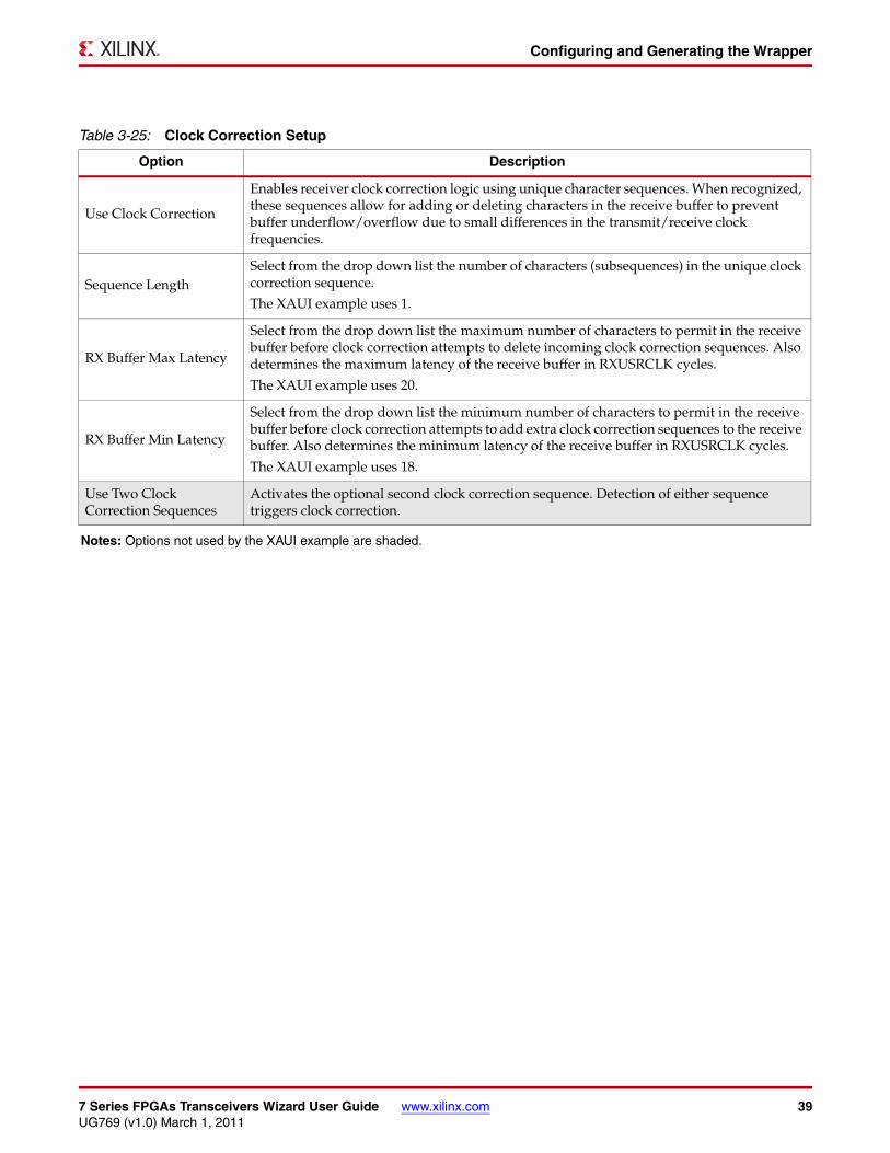
Table 3-23: Clock Correction Setup
Option Description
Use Clock Correction
Enables receiver clock correction logic using unique character sequences. When recognized, these sequences allow for adding or deleting characters in the receive buffer to prevent buffer underflow/overflow due to small differences in the transmit/receive clock frequencies.
Sequence LengthSelect from the drop down list the number of characters (subsequences) in the unique clock correction sequence.
The XAUI example uses 1.
RX Buffer Max Latency
Select from the drop down list the maximum number of characters to permit in the receive buffer before clock correction attempts to delete incoming clock correction sequences. Also determines the maximum latency of the receive buffer in RXUSRCLK cycles.
The XAUI example uses 20.
RX Buffer Min Latency
Select from the drop down list the minimum number of characters to permit in the receive buffer before clock correction attempts to add extra clock correction sequences to the receive buffer. Also determines the minimum latency of the receive buffer in RXUSRCLK cycles.
The XAUI example uses 18.
Use Two Clock Correction Sequences
Activates the optional second clock correction sequence. Detection of either sequence triggers clock correction.
Notes: Options not used by the XAUI example are shaded.
7 Series FPGAs Transceivers Wizard User Guide www.xilinx.com 37UG769 (v1.0) March 1, 2011

Chapter 3: Running the Wizard
Channel Bonding and Clock Correction SequencePage 5 of the Wizard (Figure 3-11) allow you to define the channel bonding sequence(s). Table 3-24 describes the sequence definition settings and Table 3-25, page 39 describes the clock setup settings.X-Ref Target - Figure 3-11
Figure 3-11: Channel Bonding and Clock Correction Sequence - Page 5UG769_c3_11_010911
Table 3-24: Channel Bonding and Clock Correction Sequences
Option Description
Byte (Symbol) Set each symbol to match the pattern the protocol requires. The XAUI sequence length is 8 bits. 01111100 is used for channel bonding. 00011100 is used for clock correction. The other symbols are disabled because the Sequence Length is set to 1.
K Character This option is available when 8B/10B decoding is selected. When checked, as is the case for XAUI, the symbol is an 8B/10B K character.
Inverted Disparity Some protocols with 8B/10B decoding use symbols with deliberately inverted disparity. This option should be checked when such symbols are expected in the sequence.
Don’t Care Multiple-byte sequences can have wild card symbols by checking this option. Unused bytes in the sequence automatically have this option set.
Notes: Options not used by the XAUI example are shaded.
38 www.xilinx.com 7 Series FPGAs Transceivers Wizard User GuideUG769 (v1.0) March 1, 2011
Configuring and Generating the Wrapper
Table 3-25: Clock Correction Setup
Option Description
Use Clock Correction
Enables receiver clock correction logic using unique character sequences. When recognized, these sequences allow for adding or deleting characters in the receive buffer to prevent buffer underflow/overflow due to small differences in the transmit/receive clock frequencies.
Sequence LengthSelect from the drop down list the number of characters (subsequences) in the unique clock correction sequence.
The XAUI example uses 1.
RX Buffer Max Latency
Select from the drop down list the maximum number of characters to permit in the receive buffer before clock correction attempts to delete incoming clock correction sequences. Also determines the maximum latency of the receive buffer in RXUSRCLK cycles.
The XAUI example uses 20.
RX Buffer Min Latency
Select from the drop down list the minimum number of characters to permit in the receive buffer before clock correction attempts to add extra clock correction sequences to the receive buffer. Also determines the minimum latency of the receive buffer in RXUSRCLK cycles.
The XAUI example uses 18.
Use Two Clock Correction Sequences
Activates the optional second clock correction sequence. Detection of either sequence triggers clock correction.
Notes: Options not used by the XAUI example are shaded.
7 Series FPGAs Transceivers Wizard User Guide www.xilinx.com 39UG769 (v1.0) March 1, 2011

Chapter 3: Running the Wizard
Summary Page 6 of the Wizard (Figure 3-12) provides a summary of the selected configuration parameters. After reviewing the settings, click Generate to exit and generate the wrapper.X-Ref Target - Figure 3-12
Figure 3-12: Summary - Page 6
UG769_c3_12_010911
40 www.xilinx.com 7 Series FPGAs Transceivers Wizard User GuideUG769 (v1.0) March 1, 2011

Chapter 4
Quick Start Example Design
OverviewThis chapter introduces the example design that is included with the transceiver wrappers. The example design demonstrates how to use the wrappers and demonstrates some of the key features of the GT transceiver. For detailed information about the example design, see Chapter 5, Detailed Example Design.
Functional Simulation of the Example DesignThe Transceiver Wizard provides a quick way to simulate and observe the behavior of the wrapper using the provided example design and script files.
To simulate simplex designs, the SIMPLEX_PARTNER environment variable should be set to the path of the complementary core generated to test the simplex design. For example, if a design is generated with “RX OFF”, a simplex partner design with RX enabled is needed to simulate the DUT. The SIMPLEX_PARTNER environment variable should be set to the path of the RX enabled design. The name of the simplex partner should be the same as the name of the DUT with a prefix of “tx” or ”rx” as applicable. In the current example, the name of the simplex partner design would be prefixed with “rx”.
Using ModelSimPrior to simulating the wrapper with ModelSim, the functional (gate-level) simulation models must be generated. All source files in the following directories must be compiled to a single library as shown in Table 4-1. See the Synthesis and Simulation Design Guide for ISE® 13.1 available in the ISE software documentation, for instructions on how to compile ISE simulation libraries.
The Wizard provides a command line script for use within ModelSim. To run a VHDL or Verilog ModelSim simulation of the wrapper, use the following instructions:
1. Launch the Modelsim simulator and set the current directory to
<project_directory>/<component_name>/simulation/functional
Table 4-1: Required ModelSim Simulation Libraries
HDL Library Source Directories
Verilog UNISIMS_VER<Xilinx dir>/virtex7/verilog/src/unisims<Xilinx dir>/virtex7/secureip/mti
VHDL UNISIM<Xilinx dir>/virtex7/vhdl/src/unisims/primitive<Xilinx dir>/virtex7/secureip/mti
7 Series FPGAs Transceivers Wizard User Guide www.xilinx.com 41UG769 (v1.0) March 1, 2011

Chapter 4: Quick Start Example Design
2. Set the MTI_LIBS variable:
modelsim> setenv MTI_LIBS <path to compiled libraries>
3. Launch the simulation script:
modelsim> do simulate_mti.do
The ModelSim script compiles the example design and testbench, and adds the relevant signals to the wave window.
Implementing the Example DesignWhen all of the parameters are set as desired, clicking Generate creates a directory structure under the provided Component Name. Wrapper generation proceeds and the generated output populates the appropriate subdirectories.
The directory structure for the XAUI example is provided in Chapter 5, Detailed Example Design.
After wrapper generation is complete, the results can be tested in hardware. The provided example design incorporates the wrapper and additional blocks allowing the wrapper to be driven and monitored in hardware. The generated output also includes several scripts to assist in running the Xilinx software.
From the command prompt, navigate to the project directory and type the following:
For Windows
> cd xaui_wrapper\implement> implement.bat
For Linux
% cd xaui_wrapper/implement% implement.sh
Note: Substitute Component Name string for “xaui_wrapper”.
These commands execute a script that synthesizes, builds, maps, places, and routes the example design and produces a bitmap file. The resulting files are placed in the implement/results directory.
42 www.xilinx.com 7 Series FPGAs Transceivers Wizard User GuideUG769 (v1.0) March 1, 2011

Chapter 5
Detailed Example Design
This chapter provides detailed information about the example design, including a description of files and the directory structure generated by the Xilinx® CORE Generator™ tool, the purpose and contents of the provided scripts, the contents of the example HDL wrappers, and the operation of the demonstration testbench.
Directory and File Structure<project directory>topdirectory
Top-level project directory; name is user-defined
<project directory>/<component name>opdirectory
Wizard release notes file.
<component name>/docProduct documentation
<component name>/example design Verilog and VHDL design files
<component name>/implementImplementation script files
implement/resultsResults directory, created after implementation scripts are run, and contains implement script results
<component name>/simulationSimulation scripts
simulation/functionalFunctional simulation files
7 Series FPGAs Transceivers Wizard User Guide www.xilinx.com 43UG769 (v1.0) March 1, 2011
Chapter 5: Detailed Example Design
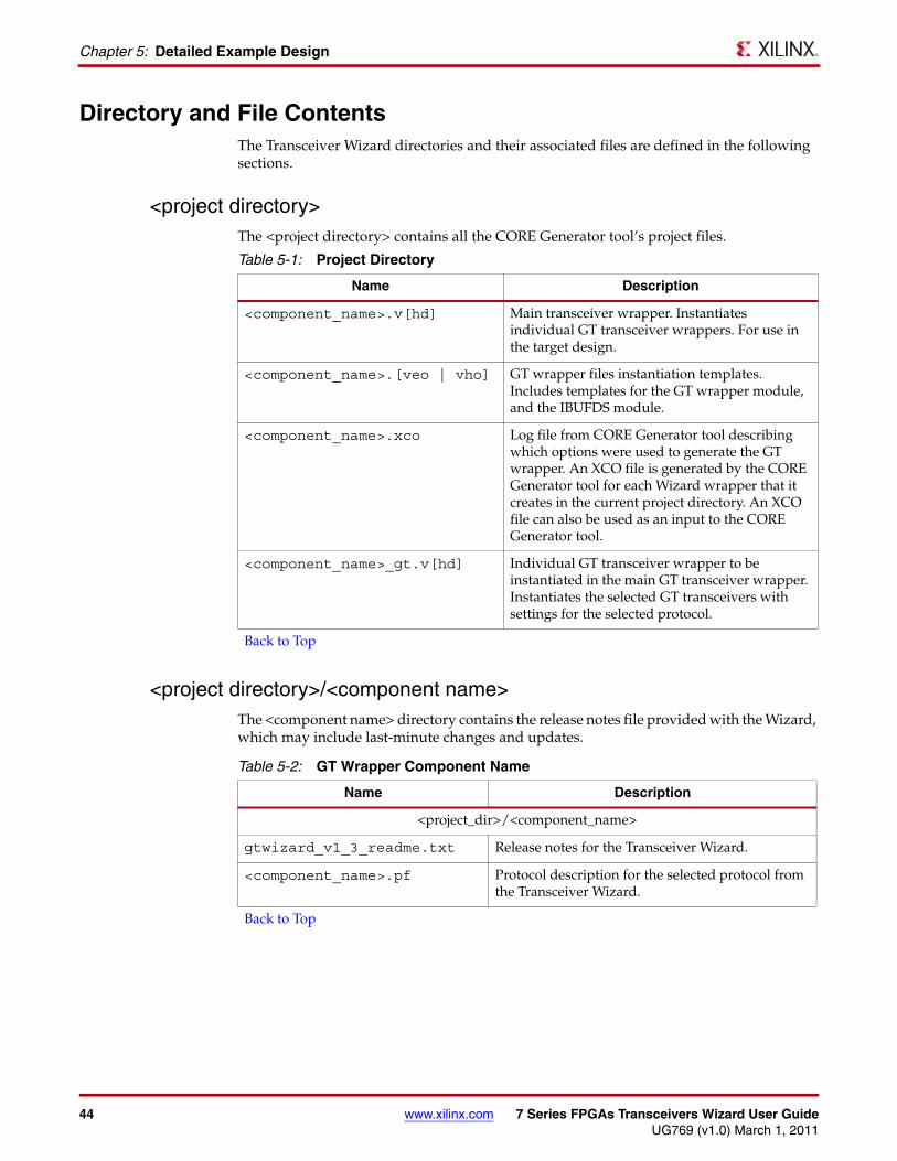
Directory and File ContentsThe Transceiver Wizard directories and their associated files are defined in the following sections.
<project directory> The <project directory> contains all the CORE Generator tool’s project files.
<project directory>/<component name> The <component name> directory contains the release notes file provided with the Wizard, which may include last-minute changes and updates.
Table 5-1: Project Directory
Name Description
<component_name>.v[hd] Main transceiver wrapper. Instantiates individual GT transceiver wrappers. For use in the target design.
<component_name>.[veo | vho] GT wrapper files instantiation templates. Includes templates for the GT wrapper module, and the IBUFDS module.
<component_name>.xco Log file from CORE Generator tool describing which options were used to generate the GT wrapper. An XCO file is generated by the CORE Generator tool for each Wizard wrapper that it creates in the current project directory. An XCO file can also be used as an input to the CORE Generator tool.
<component_name>_gt.v[hd] Individual GT transceiver wrapper to be instantiated in the main GT transceiver wrapper. Instantiates the selected GT transceivers with settings for the selected protocol.
Back to Top
Table 5-2: GT Wrapper Component Name
Name Description
<project_dir>/<component_name>
gtwizard_v1_3_readme.txt Release notes for the Transceiver Wizard.
<component_name>.pf Protocol description for the selected protocol from the Transceiver Wizard.
Back to Top
44 www.xilinx.com 7 Series FPGAs Transceivers Wizard User GuideUG769 (v1.0) March 1, 2011
Directory and File Contents
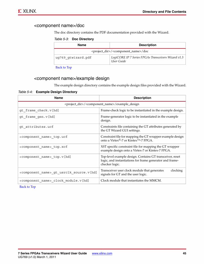
<component name>/docThe doc directory contains the PDF documentation provided with the Wizard.
<component name>/example designThe example design directory contains the example design files provided with the Wizard.
Table 5-3: Doc Directory
Name Description
<project_dir>/<component_name>/doc
ug769_gtwizard.pdf LogiCORE IP 7 Series FPGAs Transceivers Wizard v1.3 User Guide
Back to Top
Table 5-4: Example Design Directory
Name Description
<project_dir>/<component_name>/example_design
gt_frame_check.v[hd] Frame-check logic to be instantiated in the example design.
gt_frame_gen.v[hd] Frame-generator logic to be instantiated in the example design.
gt_attributes.ucf Constraints file containing the GT attributes generated by the GT Wizard GUI settings.
<component_name>_top.ucf Constraint file for mapping the GT wrapper example design onto a Virtex®-7 or Kintex™-7 FPGA.
<component_name>_top.xcf XST specific constraint file for mapping the GT wrapper example design onto a Virtex-7 or Kintex-7 FPGA.
<component_name>_top.v[hd] Top-level example design. Contains GT transceiver, reset logic, and instantiations for frame generator and frame-checker logic.
<component_name>_gt_usrclk_source.v[hd]Transceiver user clock module that generates clocking signals for GT and the user logic.
<component_name>_clock_module.v[hd] Clock module that instantiates the MMCM.
Back to Top
7 Series FPGAs Transceivers Wizard User Guide www.xilinx.com 45UG769 (v1.0) March 1, 2011

Chapter 5: Detailed Example Design
<component name>/implementThe implement directory contains the implementation script files provided with the Wizard wrapper.
implement/resultsThe results directory is created by the implement script, after which the implement script results are placed in the results directory.
<component name>/simulationThe simulation directory contains the simulation scripts provided with the Wizard wrapper.
Table 5-5: Implement Directory
Name Description
<project_dir>/<component_name>/implement
implement.bat A Windows batch file that processes the example design through the Xilinx tool flow.
implement.sh A Linux shell script that processes the example design through the Xilinx tool flow.
xst.prj The XST project file for the example design; it lists all of the source files to be synthesized.
xst.scr The XST script file for the example design that is used to synthesize the Wizard, called from the implement script described above.
Back to Top
Table 5-6: Results Directory
Name Description
<project_dir>/<component_name>/implement/results
Implement script result files.
Back to Top
Table 5-7: Simulation Directory
Name Description
<project_dir>/<component_name>/simulation
demo_tb.v[hd] Testbench to simulate the provided example design. See Functional Simulation of the Example Design, page 41.
Back to Top
46 www.xilinx.com 7 Series FPGAs Transceivers Wizard User GuideUG769 (v1.0) March 1, 2011

Directory and File Contents
simulation/functionalThe functional directory contains functional simulation scripts provided with the Wizard wrapper.
Table 5-8: Functional Directory
Name Description
<project_dir>/<component_name>/simulation/functional
simulate_mti.do ModelSim simulation script.
wave_mti.do Script for adding GT wrapper signals to the ModelSim wave viewer.
simulate_ncsim.sh Linux script for running simulation using Cadence Incisive Enterprise Simulator (IES).
simulate_vcs.sh Linux script for running simulation using Synopsys VCS and
VCS MX.
ucli_command.key Command file for VCS simulator.
vcs_session.tcl Script for adding GT wrapper signals to VCS wave window.
wave_ncsim.sv Script for adding GT - wrapper signals to the Cadence IES wave viewer.
gt_rom_init_tx.dat Block RAM initialization pattern for gt_frame_gen module. The pattern is user modifiable.
gt_rom_init_rx.dat Block RAM initialization pattern for gt_frame_check module. The pattern is user modifiable.
Back to Top
7 Series FPGAs Transceivers Wizard User Guide www.xilinx.com 47UG769 (v1.0) March 1, 2011

Chapter 5: Detailed Example Design
Example Design DescriptionThe example design that is delivered with the wrappers helps Wizard designers understand how to use the wrappers and GT transceivers in a design. The example design is shown in Figure 5-1.
The example design connects a frame generator and a frame checker to the wrapper. The frame generator transmits an incrementing counting pattern while the frame checker monitors the received data for correctness. The frame generator counting pattern is stored in BRAM. This pattern can be easily modified by altering the parameters in the gt_rom_init_tx.dat and gt_rom_init_rx.dat files. The frame checker contains the same pattern in BRAM and compares it with the received data. An error counter in the frame checker keeps a track of how many errors have occurred.
If comma alignment is enabled, the comma character will be placed within the counting pattern. Similarly, if channel bonding is enabled, the channel bonding sequence would be interspersed within the counting pattern. The frame check works by first scanning the received data for the START_OF_PACKET_CHAR. In 8B/10B designs, this is the comma alignment character. Once the START_OF_PACKET_CHAR has been found, the received data will continuously be compared to the counting pattern stored in the BRAM at each RXUSRCLK2 cycle. Once comparison has begun, if the received data ever fails to match the data in the BRAM, checking of receive data will immediately stop, an error counter will be incremented and the frame checker will return to searching for the START_OF_PACKET_CHAR.
The example design also demonstrates how to properly connect clocks to transceiver ports TXUSRCLK, TXUSRCLK2, RXUSRCLK and RXUSRCLK2. Properly configured clock module wrappers are also provided if they are required to generate user clocks for the instantiated transceivers. The logic for scrambler, descrambler and block synchronization is instantiated in the example design for 64B/66B and 64B/67B encoding.
For the example design to work properly in simulation, both the transmit and receive side need to be configured with the same line rate, encoding and datapath-width in the GUI.
X-Ref Target - Figure 5-1
Figure 5-1: Diagram of Example Design and Testbench
Example Design
Wrapper
TransceiverPorts
ConfigurationParameters
Testbench
FRAME_GEN
FRAME_CHECKTransceiver
UG769_c5_01_010611
GT_USRCLK_SOURCEModule
48 www.xilinx.com 7 Series FPGAs Transceivers Wizard User GuideUG769 (v1.0) March 1, 2011

Example Design Hierarchy
Example Design HierarchyThe hierarchy for the design used in this example is shown below.
EXAMPLE_TB |___EXAMPLE_GT_TOP |___XAUI_WRAPPER | |___XAUI_WRAPPER_GT (1 per transceiver) | |___GT_FRAME_GEN (1 per transceiver) |___GT_FRAME_CHECK (1 per transceiver) |___GT_USRCLK_SOURCE |___CLOCK_MODULE
7 Series FPGAs Transceivers Wizard User Guide www.xilinx.com 49UG769 (v1.0) March 1, 2011
Recommended