LM7171Very High Speed, High Output Current, VoltageFeedback AmplifierGeneral DescriptionThe LM7171 is a high speed voltage feedback amplifier thathas the slewing characteristic of a current feedback ampli-fier; yet it can be used in all traditional voltage feedback am-plifier configurations. The LM7171 is stable for gains as lowas +2 or −1. It provides a very high slew rate at 4100V/µsand a wide unity-gain bandwidth of 200 MHz while consum-ing only 6.5 mA of supply current. It is ideal for video andhigh speed signal processing applications such as HDSLand pulse amplifiers. With 100 mA output current, theLM7171 can be used for video distribution, as a transformerdriver or as a laser diode driver.
Operation on ±15V power supplies allows for large signalswings and provides greater dynamic range andsignal-to-noise ratio. The LM7171 offers low SFDR andTHD, ideal for ADC/DAC systems. In addition, the LM7171 isspecified for ±5V operation for portable applications.
The LM7171 is built on National’s advanced VIP™ III (Verti-cally integrated PNP) complementary bipolar process.
Features(Typical Unless Otherwise Noted)
n Easy-To-Use Voltage Feedback Topologyn Very High Slew Rate: 4100V/µsn Wide Unity-Gain Bandwidth: 200 MHzn −3 dB Frequency @ AV = +2: 220 MHzn Low Supply Current: 6.5 mAn High Open Loop Gain: 85 dBn High Output Current: 100 mAn Differential Gain and Phase: 0.01%, 0.02˚n Specified for ±15V and ±5V Operation
Applicationsn HDSL and ADSL Driversn Multimedia Broadcast Systemsn Professional Video Camerasn Video Amplifiersn Copiers/Scanners/Faxn HDTV Amplifiersn Pulse Amplifiers and Peak Detectorsn CATV/Fiber Optics Signal Processing
Typical Performance Connection Diagrams
VIP™ is a trademark of National Semiconductor Corporation.
Large Signal Pulse ResponseAV = +2, VS = ±15V
DS012385-1
8-Pin DIP/SO
DS012385-2
Top View
16-Pin Wide Body SO
DS012385-3
Top View
May 1999
LM7171
VeryH
ighS
peed,High
OutputC
urrent,VoltageFeedback
Am
plifier
© 1999 National Semiconductor Corporation DS012385 www.national.com

Ordering InformationPackage Temperature Range Transport
MediaNSC
DrawingIndustrial Military
−40˚C to +85˚C −55˚C to +125˚C
8-Pin DIP LM7171AIN, LM7171BIN Rails N08E
8-Pin CDIP LM7171AMJ-QMLLM7171AMJ-QMLV
5962-95536 Rails J08A
10-Pin CeramicSOIC
LM7171AMWG-QMLLM7171AMWG-QMLV
5962-95536 Trays WG10A
8-Pin LM7171AIM, LM7171BIM Rails M08A
Small Outline LM7171AIMX, LM7171BIMX Tape and Reel
16-Pin LM7171AIWM, LM7171BIWM Rails M16B
Small Outline LM7171AWMX, LM7171BWMX Tape and Reel
www.national.com 2
Absolute Maximum Ratings (Note 1)
If Military/Aerospace specified devices are required,please contact the National Semiconductor Sales Office/Distributors for availability and specifications.
ESD Tolerance (Note 2) 2.5 kVSupply Voltage (V+–V−) 36VDifferential Input Voltage (Note 11) ±10VOutput Short Circuit to Ground(Note 3) ContinuousStorage Temperature Range −65˚C to +150˚C
Maximum Junction Temperature(Note 4) 150˚C
Operating Ratings (Note 1)
Supply Voltage 5.5V ≤ VS ≤ 36VJunction Temperature Range
LM7171AI, LM7171BI −40˚C ≤ TJ ≤ +85˚CThermal Resistance (θJA)N Package, 8-Pin Molded DIP 108˚C/WM Package, 8-Pin Surface Mount 172˚C/WM Package, 16-Pin Surface Mount 95˚C/W
±15V DC Electrical CharacteristicsUnless otherwise specified, all limits guaranteed for TJ = 25˚C, V+ = +15V, V− = −15V, VCM = 0V, and RL = 1 kΩ. Boldfacelimits apply at the temperature extremes
Symbol Parameter Conditions Typ(Note 5)
LM7171AI LM7171BI Units
Limit Limit
(Note 6) (Note 6)
VOS Input Offset Voltage 0.2 1 3 mV
4 7 max
TC VOS Input Offset Voltage 35 µV/˚C
Average Drift
IB Input Bias Current 2.7 10 10 µA
12 12 max
IOS Input Offset Current 0.1 4 4 µA
6 6 max
RIN Input Resistance Common Mode 40 MΩDifferential Mode 3.3
RO Open Loop Output 15 ΩResistance
CMRR Common Mode VCM = ±10V 105 85 75 dB
Rejection Ratio 80 70 min
PSRR Power Supply VS = ±15V to ±5V 90 85 75 dB
Rejection Ratio 80 70 min
VCM Input Common-Mode CMRR > 60 dB ±13.35 V
Voltage Range
AV Large Signal Voltage RL = 1 kΩ 85 80 75 dB
Gain (Note 7) 75 70 min
RL = 100Ω 81 75 70 dB
70 66 min
VO Output Swing RL = 1 kΩ 13.3 13 13 V
12.7 12.7 min
−13.2 −13 −13 V
−12.7 −12.7 max
RL = 100Ω 11.8 10.5 10.5 V
9.5 9.5 min
−10.5 −9.5 −9.5 V
−9 −9 max
Output Current Sourcing, RL = 100Ω 118 105 105 mA
(Open Loop) 95 95 min
(Note 8) Sinking, RL = 100Ω 105 95 95 mA
90 90 max
www.national.com3
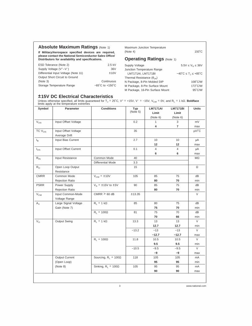
±15V DC Electrical Characteristics (Continued)
Unless otherwise specified, all limits guaranteed for TJ = 25˚C, V+ = +15V, V− = −15V, VCM = 0V, and RL = 1 kΩ. Boldfacelimits apply at the temperature extremes
Symbol Parameter Conditions Typ(Note 5)
LM7171AI LM7171BI Units
Limit Limit
(Note 6) (Note 6)
Output Current Sourcing, RL = 100Ω 100 mA
(in Linear Region) Sinking, RL = 100Ω 100
ISC Output Short Circuit Sourcing 140 mA
Current Sinking 135
IS Supply Current 6.5 8.5 8.5 mA
9.5 9.5 max
±15V AC Electrical CharacteristicsUnless otherwise specified, TJ = 25˚C, V+ = +15V, V− = −15V, VCM = 0V, and RL = 1 kΩ.
Typ LM7171AI LM7171BI
Symbol Parameter Conditions (Note 5) Limit Limit Units
(Note 6) (Note 6)
SR Slew Rate (Note 9) AV = +2, VIN = 13 VPP 4100 V/µs
AV = +2, VIN = 10 VPP 3100
Unity-Gain Bandwidth 200 MHz
−3 dB Frequency AV = +2 220 MHz
φm Phase Margin 50 Deg
ts Settling Time (0.1%) AV = −1, VO = ±5V 42 ns
RL = 500Ωtp Propagation Delay AV = −2, VIN = ±5V, 5 ns
RL = 500ΩAD Differential Gain (Note 10) 0.01 %
φD Differential Phase (Note 10) 0.02 Deg
Second Harmonic (Note 12) fIN = 10 kHz −110 dBc
fIN = 5 MHz −75 dBc
Third Harmonic (Note 12) fIN = 10 kHz −115 dBc
fIN = 5 MHz −55 dBc
en Input-Referred f = 10 kHz 14
Voltage Noise
in Input-Referred f = 10 kHz 1.5
Current Noise
±5V DC Electrical CharacteristicsUnless otherwise specified, all limits guaranteed for TJ = 25˚C, V+ = +5V, V− = −5V, VCM = 0V, and RL = 1 kΩ. Boldface lim-its apply at the temperature extremes
Typ LM7171AI LM7171BI
Symbol Parameter Conditions (Note 5) Limit Limit Units
(Note 6) (Note 6)
VOS Input Offset Voltage 0.3 1.5 3.5 mV
4 7 max
TC VOS Input Offset Voltage 35 µV/˚C
Average Drift
IB Input Bias Current 3.3 10 10 µA
12 12 max
IOS Input Offset Current 0.1 4 4 µA
www.national.com 4

±5V DC Electrical Characteristics (Continued)
Unless otherwise specified, all limits guaranteed for TJ = 25˚C, V+ = +5V, V− = −5V, VCM = 0V, and RL = 1 kΩ. Boldface lim-its apply at the temperature extremes
Typ LM7171AI LM7171BI
Symbol Parameter Conditions (Note 5) Limit Limit Units
(Note 6) (Note 6)
6 6 max
RIN Input Resistance Common Mode 40 MΩDifferential Mode 3.3
RO Output Resistance 15 ΩCMRR Common Mode VCM = ±2.5V 104 80 70 dB
Rejection Ratio 75 65 min
PSRR Power Supply VS = ±15V to ±5V 90 85 75 dB
Rejection Ratio 80 70 min
VCM Input Common-Mode CMRR > 60 dB ±3.2 V
Voltage Range
AV Large Signal Voltage RL = 1 kΩ 78 75 70 dB
Gain (Note 7) 70 65 min
RL = 100Ω 76 72 68 dB
67 63 min
VO Output Swing RL = 1 kΩ 3.4 3.2 3.2 V
3 3 min
−3.4 −3.2 −3.2 V
−3 −3 max
RL = 100Ω 3.1 2.9 2.9 V
2.8 2.8 min
−3.0 −2.9 −2.9 V
−2.8 −2.8 max
Output Current Sourcing, RL = 100Ω 31 29 29 mA
(Open Loop) (Note 8) 28 28 min
Sinking, RL = 100Ω 30 29 29 mA
28 28 max
ISC Output Short Circuit Sourcing 135 mA
Current Sinking 100
IS Supply Current 6.2 8 8 mA
9 9 max
±5V AC Electrical CharacteristicsUnless otherwise specified, TJ = 25˚C, V+ = +5V, V− = −5V, VCM = 0V, and RL = 1 kΩ.
Typ LM7171AI LM7171BI
Symbol Parameter Conditions (Note 5) Limit Limit Units
(Note 6) (Note 6)
SR Slew Rate (Note 9) AV = +2, VIN = 3.5 VPP 950 V/µs
Unity-Gain Bandwidth 125 MHz
−3 dB Frequency AV = +2 140 MHz
φm Phase Margin 57 Deg
ts Settling Time (0.1%) AV = −1, VO = ±1V, 56 ns
RL = 500Ωtp Propagation Delay AV = −2, VIN = ±1V, 6 ns
RL = 500ΩAD Differential Gain (Note 1) 0.02 %
www.national.com5

±5V AC Electrical Characteristics (Continued)
Unless otherwise specified, TJ = 25˚C, V+ = +5V, V− = −5V, VCM = 0V, and RL = 1 kΩ.
Typ LM7171AI LM7171BI
Symbol Parameter Conditions (Note 5) Limit Limit Units
(Note 6) (Note 6)
φD Differential Phase (Note 10) 0.03 Deg
Second Harmonic (Note 12) fIN = 10 kHz −102 dBc
fIN = 5 MHz −70 dBc
Third Harmonic (Note 12) fIN = 10 kHz −110 dBc
fIN = 5 MHz −51 dBc
en Input-Referred f = 10 kHz 14
Voltage Noise
in Input-Referred f = 10 kHz 1.8
Current Noise
Note 1: Absolute Maximum Ratings indicate limits beyond which damage to the device may occur. Operating Ratings indicate conditions for which the device is in-tended to be functional, but specific performance is not guaranteed. For guaranteed specifications and the test conditions, see the Electrical Characteristics.
Note 2: Human body model, 1.5 kΩ in series with 100 pF.
Note 3: Applies to both single-supply and split-supply operation. Continuous short circuit operation at elevated ambient temperature can result in exceeding themaximum allowed junction temperature of 150˚C.
Note 4: The maximum power dissipation is a function of TJ(max), θJA, and TA. The maximum allowable power dissipation at any ambient temperature is PD =(TJ(max)–TA)/θJA. All numbers apply for packages soldered directly into a PC board.
Note 5: Typifcal values represent the most likely parametric norm.
Note 6: All limits are guaranteed by testing or statistical analysis.
Note 7: Large signal voltage gain is the total output swing divided by the input signal required to produce that swing. For VS = ±15V, VOUT = ±5V. For VS = ±5V,VOUT = ±1V.
Note 8: The open loop output current is guaranteed, by the measurement of the open loop output voltage swing, using 100Ω output load.
Note 9: Slew Rate is the average of the raising and falling slew rates.
Note 10: Differential gain and phase are measured with AV = +2, VIN = 1 VPP at 3.58 MHz and both input and output 75Ω terminated.
Note 11: Input differential voltage is applied at VS = ±15V.
Note 12: Harmonics are measured with VIN = 1 VPP, AV = +2 and RL = 100Ω.
Typical Performance Characteristics unless otherwise noted, TA= 25˚C
Supply Currentvs Supply Voltage
DS012385-63
Supply Currentvs Temperature
DS012385-64
Input Offset Voltagevs Temperature
DS012385-65
www.national.com 6

Typical Performance Characteristics unless otherwise noted, TA= 25˚C (Continued)
Input Bias Currentvs Temperature
DS012385-66
Short Circuit Currentvs Temperature (Sourcing)
DS012385-67
Short Circuit Currentvs Temperature (Sinking)
DS012385-68
Output Voltagevs Output Current
DS012385-69
Output Voltagevs Output Current
DS012385-70
CMRR vs Frequency
DS012385-71
PSRR vs Frequency
DS012385-72
PSRR vs Frequency
DS012385-73
Open Loop FrequencyResponse
DS012385-51
Open Loop FrequencyResponse
DS012385-52
Gain-Bandwidth Productvs Supply Voltage
DS012385-53
www.national.com7

Typical Performance Characteristics unless otherwise noted, TA= 25˚C (Continued)
Gain-Bandwidth Productvs Load Capacitance
DS012385-54
Large Signal Voltage Gainvs Load
DS012385-55
Large Signal Voltage Gainvs Load
DS012385-56
Input Voltage Noisevs Frequency
DS012385-57
Input Voltage Noisevs Frequency
DS012385-58
Input Current Noisevs Frequency
DS012385-59
Input Current Noisevs Frequency
DS012385-60
Slew Ratevs Supply Voltage
DS012385-61
Slew Ratevs Input Voltage
DS012385-62
www.national.com 8

Typical Performance Characteristics unless otherwise noted, TA= 25˚C (Continued)
Slew Ratevs Load Capacitance
DS012385-23
Open Loop OutputImpedance vs Frequency
DS012385-25
Open Loop OutputImpedance vs Frequency
DS012385-26
Large Signal PulseResponse A V = −1,VS = ±15V
DS012385-27
Large Signal PulseResponse A V = −1,VS = ±5V
DS012385-28
Large Signal PulseResponse A V = +2,VS = ±15V
DS012385-29
Large Signal PulseResponse A V = +2,VS = ±5V
DS012385-30
Small Signal PulseResponse A V = −1,VS = ±15V
DS012385-31
Small Signal PulseResponse A V = −1,VS = ±5V
DS012385-32
www.national.com9

Typical Performance Characteristics unless otherwise noted, TA= 25˚C (Continued)
Small Signal PulseResponse A V = +2,VS = ±15V
DS012385-33
Small Signal PulseResponse A V = +2,VS = ±5V
DS012385-34
Closed Loop FrequencyResponse vs SupplyVoltage (A V = +2)
DS012385-35
Closed Loop FrequencyResponse vs CapacitiveLoad (A V = +2)
DS012385-36
Closed Loop FrequencyResponse vs CapacitiveLoad (A V = +2)
DS012385-37
Closed Loop FrequencyResponse vs Input SignalLevel (A V = +2)
DS012385-38
Closed Loop FrequencyResponse vs Input SignalLevel (A V = +2)
DS012385-43
Closed Loop FrequencyResponse vs Input SignalLevel (A V = +2)
DS012385-39
Closed Loop FrequencyResponse vs Input SignalLevel (A V = +2)
DS012385-40
www.national.com 10

Typical Performance Characteristics unless otherwise noted, TA= 25˚C (Continued)
Closed Loop FrequencyResponse vs Input SignalLevel (A V = +4)
DS012385-44
Closed Loop FrequencyResponse vs Input SignalLevel (A V = +4)
DS012385-45
Closed Loop FrequencyResponse vs Input SignalLevel (A V = +4)
DS012385-41
Closed Loop FrequencyResponse vs Input SignalLevel (A V = +4)
DS012385-42
Total Harmonic Distortionvs Frequency (Note 13)
DS012385-46
Total Harmonic Distortionvs Frequency (Note 13)
DS012385-47
Undistorted Output Swingvs Frequency
DS012385-49
Undistorted Output Swingvs Frequency
DS012385-48
Undistorted Output Swingvs Frequency
DS012385-50
www.national.com11

Typical Performance Characteristics unless otherwise noted, TA= 25˚C (Continued)
Note 13: The THD measurement at low frequency is limited by the test instrument.
Simplified Schematic Diagram
Application Notes
LM7171 Performance DiscussionThe LM7171 is a very high speed, voltage feedback ampli-fier. It consumes only 6.5 mA supply current while providinga unity-gain bandwidth of 200 MHz and a slew rate of 4100V/µs. It also has other great features such as low differentialgain and phase and high output current.
The LM7171 is a true voltage feedback amplifier. Unlike cur-rent feedback amplifiers (CFAs) with a low inverting input im-pedance and a high non-inverting input impedance, both in-puts of voltage feedback amplifiers (VFAs) have highimpedance nodes. The low impedance inverting input in
CFAs and a feedback capacitor create an additional polethat will lead to instability. As a result, CFAs cannot be usedin traditional op amp circuits such as photodiode amplifiers,I-to-V converters and integrators where a feedback capacitoris required.
LM7171 Circuit OperationThe class AB input stage in LM7171 is fully symmetrical andhas a similar slewing characteristic to the current feedbackamplifiers. In the LM7171 Simplified Schematic, Q1 throughQ4 form the equivalent of the current feedback input buffer,RE the equivalent of the feedback resistor, and stage A buff-
Harmonic Distortionvs Frequency
DS012385-74
Harmonic Distortionvs Frequency
DS012385-75
Maximum Power Dissipationvs Ambient Temperature
DS012385-20
DS012385-9
Note: M1 and M2 are current mirrors.
www.national.com 12
LM7171 Circuit Operation (Continued)
ers the inverting input. The triple-buffered output stage iso-lates the gain stage from the load to provide low output im-pedance.
LM7171 Slew Rate CharacteristicThe slew rate of LM7171 is determined by the current avail-able to charge and discharge an internal high impedancenode capacitor. This current is the differential input voltagedivided by the total degeneration resistor RE. Therefore, theslew rate is proportional to the input voltage level, and thehigher slew rates are achievable in the lower gain configura-tions. A curve of slew rate versus input voltage level is pro-vided in the “Typical Performance Characteristics”.
When a very fast large signal pulse is applied to the input ofan amplifier, some overshoot or undershoot occurs. By plac-ing an external resistor such as 1 kΩ in series with the inputof LM7171, the bandwidth is reduced to help lower the over-shoot.
Slew Rate LimitationIf the amplifier’s input signal has too large of an amplitude attoo high of a frequency, the amplifier is said to be slew ratelimited; this can cause ringing in time domain and peaking infrequency domain at the output of the amplifier.
In the “Typical Performance Characteristics” section, thereare several curves of AV = +2 and AV = +4 versus input sig-nal levels. For the AV = +4 curves, no peaking is present andthe LM7171 responds identically to the different input signallevels of 30 mV, 100 mV and 300 mV.
For the AV = +2 curves, with slight peaking occurs. Thispeaking at high frequency (>100 MHz) is caused by a largeinput signal at high enough frequency that exceeds the am-plifier’s slew rate. The peaking in frequency response doesnot limit the pulse response in time domain, and the LM7171is stable with noise gain of ≥+2.
Layout Consideration
PRINTED CIRCUIT BOARDS AND HIGH SPEED OPAMPS
There are many things to consider when designing PCboards for high speed op amps. Without proper caution, it isvery easy to have excessive ringing, oscillation and other de-graded AC performance in high speed circuits. As a rule, thesignal traces should be short and wide to provide low induc-tance and low impedance paths. Any unused board spaceneeds to be grounded to reduce stray signal pickup. Criticalcomponents should also be grounded at a common point toeliminate voltage drop. Sockets add capacitance to theboard and can affect high frequency performance. It is betterto solder the amplifier directly into the PC board without us-ing any socket.
USING PROBES
Active (FET) probes are ideal for taking high frequency mea-surements because they have wide bandwidth, high inputimpedance and low input capacitance. However, the probeground leads provide a long ground loop that will produce er-rors in measurement. Instead, the probes can be groundeddirectly by removing the ground leads and probe jackets andusing scope probe jacks.
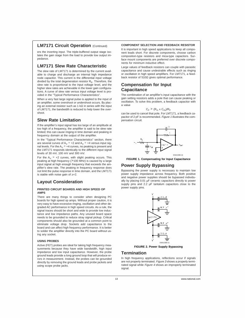
COMPONENT SELECTION AND FEEDBACK RESISTOR
It is important in high speed applications to keep all compo-nent leads short. For discrete components, choose carboncomposition-type resistors and mica-type capacitors. Sur-face mount components are preferred over discrete compo-nents for minimum inductive effect.
Large values of feedback resistors can couple with parasiticcapacitance and cause undesirable effects such as ringingor oscillation in high speed amplifiers. For LM7171, a feed-back resistor of 510Ω gives optimal performance.
Compensation for InputCapacitanceThe combination of an amplifier’s input capacitance with thegain setting resistors adds a pole that can cause peaking oroscillation. To solve this problem, a feedback capacitor witha value
CF > (RG x CIN)/RF
can be used to cancel that pole. For LM7171, a feedback ca-pacitor of 2 pF is recommended. Figure 1 illustrates the com-pensation circuit.
Power Supply BypassingBypassing the power supply is necessary to maintain lowpower supply impedance across frequency. Both positiveand negative power supplies should be bypassed individu-ally by placing 0.01 µF ceramic capacitors directly to powersupply pins and 2.2 µF tantalum capacitors close to thepower supply pins.
TerminationIn high frequency applications, reflections occur if signalsare not properly terminated. Figure 3 shows a properly termi-nated signal while Figure 4 shows an improperly terminatedsignal.
DS012385-10
FIGURE 1. Compensating for Input Capacitance
DS012385-11
FIGURE 2. Power Supply Bypassing
www.national.com13

Termination (Continued)
To minimize reflection, coaxial cable with matching charac-teristic impedance to the signal source should be used. Theother end of the cable should be terminated with the samevalue terminator or resistor. For the commonly used cables,RG59 has 75Ω characteristic impedance, and RG58 has50Ω characteristic impedance.
Driving Capacitive LoadsAmplifiers driving capacitive loads can oscillate or have ring-ing at the output. To eliminate oscillation or reduce ringing,an isolation resistor can be placed as shown below in Figure5 The combination of the isolation resistor and the load ca-pacitor forms a pole to increase stability by adding morephase margin to the overall system. The desired perfor-mance depends on the value of the isolation resistor; the big-ger the isolation resistor, the more damped the pulse re-sponse becomes. For LM7171, a 50Ω isolation resistor isrecommended for initial evaluation. Figure 6 shows theLM7171 driving a 150 pF load with the 50Ω isolation resistor.
Power DissipationThe maximum power allowed to dissipate in a device is de-fined as:
PD = (TJ(max) − TA)/θJA
Where
PD is the power dissipation in a device
TJ(max) is the maximum junction temperature
TA is the ambient temperature
θJA is the thermal resistance of a particular package
For example, for the LM7171 in a SO-8 package, the maxi-mum power dissipation at 25˚C ambient temperature is730 mW.
Thermal resistance, θJA, depends on parameters such asdie size, package size and package material. The smallerthe die size and package, the higher θJA becomes. The 8-pinDIP package has a lower thermal resistance (108˚C/W) thanthat of 8-pin SO (172˚C/W). Therefore, for higher dissipationcapability, use an 8-pin DIP package.
The total power dissipated in a device can be calculated as:
PD = PQ + PL
PQ is the quiescent power dissipated in a device with no loadconnected at the output. PL is the power dissipated in the de-vice with a load connected at the output; it is not the powerdissipated by the load.
Furthermore,
PQ: = supply current x total supply voltage with no load
PL: = output current x (voltage difference betweensupply voltage and output voltage of the sameside of supply voltage)
DS012385-17
FIGURE 3. Properly Terminated Signal
DS012385-18
FIGURE 4. Improperly Terminated Signal
DS012385-12
FIGURE 5. Isolation Resistor Usedto Drive Capacitive Load
DS012385-13
FIGURE 6. The LM7171 Driving a 150 pF Loadwith a 50 Ω Isolation Resistor
www.national.com 14

Power Dissipation (Continued)
For example, the total power dissipated by the LM7171 withVS = ±15V and output voltage of 10V into 1 kΩ is
PD = PQ + PL
= (6.5 mA) x (30V) + (10 mA) x (15V − 10V)= 195 mW + 50 mW= 245 mW
Application Circuit
Fast Instrumentation Amplifier
DS012385-14
DS012385-80
Multivibrator
DS012385-15
DS012385-81
Pulse Width Modulator
DS012385-16
www.national.com15

Application Circuit (Continued)
Video Line Driver
DS012385-21
www.national.com 16

Design KitA design kit is available for the LM7171. The design kit con-tains:
• High Speed Evaluation Board
• LM7171 in 8-pin DIP Package
• LM7171 Datasheet
• Pspice Macromodel DIskette With The LM7171 Macro-model
• Amplifier Selection Guide
Pitch PackA pitch pack is available for the LM7171. The pitch pack con-tains:
• LM7171 in 8-pin DIP Package
• LM7171 Datasheet
• Pspice Macromodel DIskette With The LM7171 Macro-model
• Amplifier Selection Guide
Contact your local National Semiconductor sales office toobtain a pitch pack and design kit.
www.national.com17
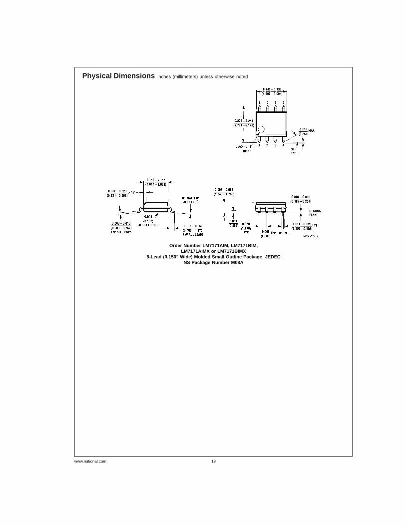
Physical Dimensions inches (millimeters) unless otherwise noted
Order Number LM7171AIM, LM7171BIM,LM7171AIMX or LM7171BIMX
8-Lead (0.150" Wide) Molded Small Outline Package, JEDECNS Package Number M08A
www.national.com 18

Physical Dimensions inches (millimeters) unless otherwise noted (Continued)
Order Number LM7171AIWM, LM7171BIWM,LM7171AIWMX or LM7171BIWMX
16-Lead (0.300" Wide) Molded Small Outline Package, JEDECNS Package Number M16B
Order Number LM7171AIN or LM7171BIN8-Lead (0.300" Wide) Molded Dual-In-Line Package, JEDEC
NS Package Number N08E
www.national.com19

Physical Dimensions inches (millimeters) unless otherwise noted (Continued)
LIFE SUPPORT POLICY
NATIONAL’S PRODUCTS ARE NOT AUTHORIZED FOR USE AS CRITICAL COMPONENTS IN LIFE SUPPORTDEVICES OR SYSTEMS WITHOUT THE EXPRESS WRITTEN APPROVAL OF THE PRESIDENT AND GENERALCOUNSEL OF NATIONAL SEMICONDUCTOR CORPORATION. As used herein:
1. Life support devices or systems are devices orsystems which, (a) are intended for surgical implantinto the body, or (b) support or sustain life, andwhose failure to perform when properly used inaccordance with instructions for use provided in thelabeling, can be reasonably expected to result in asignificant injury to the user.
2. A critical component is any component of a lifesupport device or system whose failure to performcan be reasonably expected to cause the failure ofthe life support device or system, or to affect itssafety or effectiveness.
National SemiconductorCorporationAmericasTel: 1-800-272-9959Fax: 1-800-737-7018Email: [email protected]
National SemiconductorEurope
Fax: +49 (0) 1 80-530 85 86Email: [email protected]
Deutsch Tel: +49 (0) 1 80-530 85 85English Tel: +49 (0) 1 80-532 78 32Français Tel: +49 (0) 1 80-532 93 58Italiano Tel: +49 (0) 1 80-534 16 80
National SemiconductorAsia Pacific CustomerResponse GroupTel: 65-2544466Fax: 65-2504466Email: [email protected]
National SemiconductorJapan Ltd.Tel: 81-3-5639-7560Fax: 81-3-5639-7507
www.national.com
Order Number 5962-9553601QPA8-Lead Dual-In-Line Package
NS Package Number J08ANSID is LM7171AMJ/883
LM71
71Ve
ryH
igh
Spe
ed,H
igh
Out
putC
urre
nt,V
olta
geFe
edba
ckA
mpl
ifier
National does not assume any responsibility for use of any circuitry described, no circuit patent licenses are implied and National reserves the right at any time without notice to change said circuitry and specifications.
Recommended