Lecture #3 PIC Microcontrollers
Instructor: Dr. Ahmad El-Banna
SPR
IN
G 2
015
E-626-A Real-Time Embedded Systems (RTES)
Integrated Technical Education Cluster At AlAmeeria
© A
hmad
El-B
anna

Agenda
What’s a Microcontroller?
Types of Microcontrollers
Features and Internal structure of PIC 16F877A
Instruction Execution 2
RTES
, Lec
#3 , S
prin
g 201
5 ©
Ahm
ad E
l-Ban
na

What is a microcontroller?
• A microcontroller (sometimes abbreviated µC, uC or
MCU) is a small computer on a single integrated circuit
containing a processor core, memory, and
programmable input/output peripherals.
• It can only perform simple/specific tasks.
• A microcontroller is often described as a ‘computer-on-a-
chip’.
3
RTES
, Lec
#3 , S
prin
g 201
5 ©
Ahm
ad E
l-Ban
na

Microcomputer system and Microcontroller based system
4
RTES
, Lec
#3 , S
prin
g 201
5 ©
Ahm
ad E
l-Ban
na

Microcontrollers..
• Microcontrollers are purchased ‘blank’ and then programmed with a specific control program.
• Once programmed the microcontroller is build into a product to make the product more intelligent and easier to use.
• A designer will use a Microcontroller to:
• Gather input from various sensors
• Process this input into a set of actions
• Use the output mechanisms on the microcontroller to do something useful.
5
RTES
, Lec
#3 , S
prin
g 201
5 ©
Ahm
ad E
l-Ban
na

Types of Microcontrollers
• Parallax Propeller • Freescale 68HC11 (8-bit) • Intel 8051 • Silicon Laboratories Pipelined 8051 Microcontrollers • ARM processors (from many vendors) using ARM7 or Cortex-M3
cores are generally microcontrollers • STMicroelectronics STM8 (8-bit), ST10 (16-bit) and STM32 (32-bit) • Atmel AVR (8-bit), AVR32 (32-bit), and AT91SAM (32-bit) • Freescale ColdFire (32-bit) and S08 (8-bit) • Hitachi H8, Hitachi SuperH (32-bit) • Hyperstone E1/E2 (32-bit, First full integration of RISC and DSP on
one processor core [1996]) • Infineon Microcontroller: 8, 16, 32 Bit microcontrollers for
automotive and industrial applications.
6
RTES
, Lec
#3 , S
prin
g 201
5 ©
Ahm
ad E
l-Ban
na

Types of Microcontrollers..
• MIPS (32-bit PIC32)
• NEC V850 (32-bit)
• Microchip PIC (8-bit PIC16, PIC18, 16-bit dsPIC33/PIC24)
• PowerPC ISE
• PSoC (Programmable System-on-Chip)
• Rabbit 2000 (8-bit)
• Texas Instruments Microcontroller MSP 430 (16-bit), C2000 (32-bit), and Stellaris (32-bit)
• Toshiba TLCS-870 (8-bit/16-bit)
• Zilog eZ8 (16-bit), eZ80 (8-bit)
• etc
7
RTES
, Lec
#3 , S
prin
g 201
5 ©
Ahm
ad E
l-Ban
na

Microcontroller Packaging and Appearance
8
RTES
, Lec
#3 , S
prin
g 201
5 ©
Ahm
ad E
l-Ban
na
From left to right: PIC 12F508, PIC 16F84A, PIC 16C72, Motorola 68HC05B16, PIC 16F877, Motorola 68000

PIC Microcontrollers
• Peripheral Interface Controller (PIC) was originally designed by General Instruments
• In the late 1970s, GI introduced PIC® 1650 and 1655 – RISC with 30 instructions.
• PIC was sold to Microchip
• Features: low-cost, self-contained, 8-bit, Harvard structure, pipelined, RISC, single accumulator, with fixed reset and interrupt vectors.
9
RTES
, Lec
#3 , S
prin
g 201
5 ©
Ahm
ad E
l-Ban
na

PIC Microcontroller product family
10
RTES
, Lec
#3 , S
prin
g 201
5 ©
Ahm
ad E
l-Ban
na
• 8-bit microcontrollers
• PIC10
• PIC12
• PIC14
• PIC16
• PIC17
• PIC18
• 16-bit microcontrollers
• PIC24F
• PIC24H
• 32-bit microcontrollers
• PIC32
• 16-bit digital signal controllers • dsPIC30
• dsPIC33F

PIC Microcontroller product family..
11
RTES
, Lec
#3 , S
prin
g 201
5 ©
Ahm
ad E
l-Ban
na
• The F in a name generally indicates the PICmicro uses flash memory and can be erased electronically.
• The C generally means it can only be erased by exposing the die to ultraviolet light (which is only possible if a windowed package style is used). An exception to this rule is the PIC16C84 which uses EEPROM and is therefore electrically erasable.

An Example: PIC16F877
• Why PIC16F877A is very popular?
• This is because PIC16F877A is very cheap. Apart from that it is also very easy to be assembled. Additional components that you need to make this IC work is just a 5V power supply adapter, a 20MHz crystal oscillator and 2 units of 22pF capacitors.
• What is the advantages of PIC16F877A?
• This IC can be reprogrammed and erased up to 10,000 times. Therefore it is very good for new product development phase.
• What is the disadvantages of PIC16F877A?
• This IC has no internal oscillator so you will need an external crystal of other clock source.
12
RTES
, Lec
#3 , S
prin
g 201
5 ©
Ahm
ad E
l-Ban
na
Feat
ure
s
13
RTES
, Lec
#3 , S
prin
g 201
5 ©
Ahm
ad E
l-Ban
na
Key Features PIC16F877
MAX Operating Frequency 20MHz
FLASH Program Memory
(14-bit words) 8K
Data Memory (bytes) 368
EEPROM Data Memory (bytes) 256
I/O Ports
RA0-5 (6)
RB0-7 (8)
RC0-7 (8)
RD0-7 (8)
RE0-2 (3)
Timers 3
CCP ( Capture/Compare/PWM) 2
Serial Communications MSSP, USART
Parallel Communications PSP
10-bit Analog-to-Digital Module 8 Channels
Instruction Set 35 Instructions
Pins (DIP) 40 Pins

Bubble diagram of PIC16F877
14
RTES
, Lec
#3 , S
prin
g 201
5 ©
Ahm
ad E
l-Ban
na

Pin Diagram of PIC16F877
15
RTES
, Lec
#3 , S
prin
g 201
5 ©
Ahm
ad E
l-Ban
na
Quad Flat
Package (QFP)
Plastic Leaded Chip Carrier
Package (PLCC)

Pin Diagram of PIC16F877..
16
RTES
, Lec
#3 , S
prin
g 201
5 ©
Ahm
ad E
l-Ban
na
• Plastic dual in-line package (DIP)

PIC16F877 Architecture
17
RTES
, Lec
#3 , S
prin
g 201
5 ©
Ahm
ad E
l-Ban
na

PIC16F877 Internal Block Diagram
• The basic architecture of PIC16F877 consists of Program memory, file registers and RAM, ALU and CPU registers.
18
RTES
, Lec
#3 , S
prin
g 201
5 ©
Ahm
ad E
l-Ban
na

Memory of the PIC16F877
• divided into 3 types of memories:
1. Program Memory – A memory that contains the program (which we had written), after we've burned it. As a reminder, Program Counter executes commands stored in the program memory, one after the other.
2. Data Memory – This is RAM memory type, which contains a special registers like SFR (Special Function Register) and GPR (General Purpose Register). The variables that we store in the Data Memory during the program are deleted after we turn off the micro. These two memories have separated data buses, which makes the access to each one of them very easy.
3. Data EEPROM (Electrically Erasable Programmable Read-Only Memory) – A memory that allows storing the variables as a result of burning the written program. 19
RTES
, Lec
#3 , S
prin
g 201
5 ©
Ahm
ad E
l-Ban
na

Memory of the PIC16F877..
• Each one of them has a different role. Program Memory and Data Memory two memories that are needed to build a program, and Data EEPROM is used to save data after the microcontroller is turn off.
20
RTES
, Lec
#3 , S
prin
g 201
5 ©
Ahm
ad E
l-Ban
na

PIC16F877A Program Memory
• Is Flash Memory • Used for storing
compiled code (user’s program)
• Program Memory capacity is 8K x 14 bit Each location is 14 bits long
Every instruction is coded as a 14 bit word
• PC can address up to 8K addresses
• Addresses H’000’ and H’004’ are treated in a special way
21
RTES
, Lec
#3 , S
prin
g 201
5 ©
Ahm
ad E
l-Ban
na

PIC16F877A Data Memory (RAM)
• Memory storage for variables
• Data Memory is also known as Register File and consists of two components. • General purpose register file (same as RAM).
• Special purpose register file (similar to SFR in 8051).
• Addresses range from 0 to 511 and partitioned into 4 banks each bank extends up to 7Fh (128 bytes).
• The user can only access a RAM byte in a set of 4 banks and only one bank at a time. The default bank is BANK0.
• To access a register that is located in another bank, one should access it inside the program. There are special registers which can be accessed from any bank, such as STATUS register.
22
RTES
, Lec
#3 , S
prin
g 201
5 ©
Ahm
ad E
l-Ban
na

PIC16F877A Registers
• Some CPU Registers:
• W
• PC
• FSR
• IDF
• PCL
• PCLATH
• STATUS
23
RTES
, Lec
#3 , S
prin
g 201
5 ©
Ahm
ad E
l-Ban
na

W Register
• W, the working register, is used by many instructions as the source of an operand. This is similar to accumulator in 8051.
• It may also serve as the destination for the result of the instruction execution. It is an 8-bit register.
24
RTES
, Lec
#3 , S
prin
g 201
5 ©
Ahm
ad E
l-Ban
na

Program Counter
• Program Counter (PC) is 13 bit and capable of addressing an 8K word x 14 bit program memory space.
• PC keeps track of the program execution by holding the address of the current instruction.
• It is automatically incremented to the next instruction during the current instruction execution.
• Program Counter Stack • an independent 8-level stack is used for the program counter. • As the PC is 13-bit, the stack is organized as 8x13bit registers. • When an interrupt occurs, the PC is pushed onto the stack. When
the interrupt is being served, other interrupts remain disabled. Hence, other 7 registers of the stack can be used for subroutine calls within an interrupt service routine or within the mainline program.
25
RTES
, Lec
#3 , S
prin
g 201
5 ©
Ahm
ad E
l-Ban
na

FSR & INDF
• FSR Register
• (File Selection Register, address = 04H, 84H)
is an 8-bit register used as data memory address pointer. This is used in indirect addressing mode.
• INDF Register
• (INDirect through FSR, address = 00H, 80H)
INDF is not a physical register. Accessing INDF is actually access the location pointed to by FSR in indirect addressing mode.
26
RTES
, Lec
#3 , S
prin
g 201
5 ©
Ahm
ad E
l-Ban
na
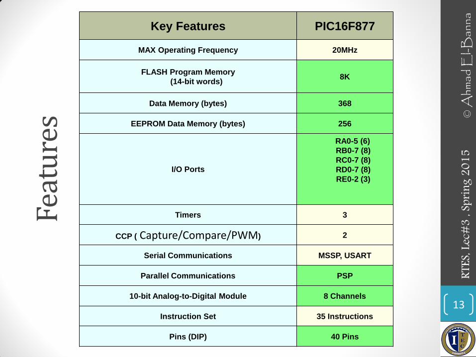
PCL & PCLATH
• PCL Register • (Program Counter Low Byte, address =02H, 82H)
PCL is actually the lower 8-bits of the 13-bit Program Counter. This is a both readable and writable register.
• PCLATH Register • (Program Counter LATcH, address = 0AH, 8AH)
PCLATH is a 8-bit register which can be used to decide the upper 5-bits of the PC. PCLATH is not the upper 5bits of the PC. PCLATH can be read from or written to without affecting the PC. The upper 3 bits of PCLATH remain zero and they serve no purpose. When PCL is written to, the lower 5bits of PCLATH are automatically loaded to the upper 5bits of the PC.
27
RTES
, Lec
#3 , S
prin
g 201
5 ©
Ahm
ad E
l-Ban
na

Memory Map Registers
• In order to start programming and build automated system, there is no need to study all the registers of the memory map, but only a few most important ones:
• STATUS register – changes/moves from/between the banks.
• PORT registers – assigns logic values (“0”/”1”) to the ports
• TRIS registers – data direction register (input/output)
28
RTES
, Lec
#3 , S
prin
g 201
5 ©
Ahm
ad E
l-Ban
na

STATUS Register
• Is an 8-bit register that stores the status of the processor.
• In most cases, this register is used to switch between the banks (Register Bank Select), but also has other capabilities.
• IRP - Register Bank Select bit.
• RP1:RP0: - Register Bank Select bits.
• TO: Time-out bit
• PD: Power-down bit
• Z: Zero bit
• DC: Digit carry/borrow bit
• C: Carry/borrow bit
29
RTES
, Lec
#3 , S
prin
g 201
5 ©
Ahm
ad E
l-Ban
na
Used in conjunction with PIC’s sleep mode

PIC16F877 Peripheral features
1. I/O Ports:
• PIC16F877 has 5 I/O ports:
• PORT A has 6 bit wide, Bidirectional
• PORT B, C, D have 8 bit wide, Bidirectional
• PORT E has 3 bit wide, Bidirectional
• In addition, they have the following alternate functions:
30
RTES
, Lec
#3 , S
prin
g 201
5 ©
Ahm
ad E
l-Ban
na

PIC16F877 Peripheral features..
• Each port has 2 control registers: • TRISx sets whether each pin is an input(1) or
output(0)
• PORTx sets their output bit levels or contain their input bit levels.
• Pin functionality “overloaded” with other features.
• Most pins have 25mA source/sink thus it can drive LEDs directly.
31
RTES
, Lec
#3 , S
prin
g 201
5 ©
Ahm
ad E
l-Ban
na

PIC16F877 Peripheral features…
2. Analog to Digital Converter (ADC) • Only available in 14bit and 16bit cores • Fs (sample rate) < 54KHz • The result is a 10 bit digital number • Can generate an interrupt when ADC conversion is done • The A/D module has 4 registers:
• A/D Result High Register (ADRESH) • A/D Result Low Register (ADRESL) • A/D Control Register0 (ADCON0) • A/D Control Register1 (ADCON1)
• Multiplexed 8 channel inputs • Must wait T acq to change up sampling capacitor.
• Can take a reference voltage different from that of the controller.
32
RTES
, Lec
#3 , S
prin
g 201
5 ©
Ahm
ad E
l-Ban
na

PIC16F877 Peripheral features….
3. Timer/counter modules • Generate interrupts on timer overflow
• Can use external pins as clock in/ clock out (ie. for counting events or using a different Fosc)
• There are 3 Timer/counter modules:
• Timer0: 8-bit timer/counter with 8-bit pre-scaler
• Timer1: 16-bit timer/counter with 8-bit pre-scaler, can be incremented during SLEEP via external crystal/clock
• Timer2: 8-bit timer/counter with 8-bit period register, pre-scaler and post-scaler.
33
RTES
, Lec
#3 , S
prin
g 201
5 ©
Ahm
ad E
l-Ban
na

PIC16F877 Peripheral features…..
4. Universal Synchronous Asynchronous Receiver Transmitter (USART/SCI) with 9-bit address detection.
• Asynchronous communication: UART (RS 232 serial) • Can do 300bps – 115kbps • 8 or 9 bits, parity, start and stop bits, etc. • Outputs 5V needs a RS232 level converter (e.g
MAX232) • Synchronous communication: i.e with clock signal
• SPI = Serial Peripheral Interface • 3 wire: Data in, Data out, Clock • Master/Slave (can have multiple masters) • Very high speed (1.6Mbps) • Full speed simultaneous send and receive (Full duplex)
• I2C = Inter IC • 2 wire: Data and Clock • Master/Slave (Single master only) • Lots of cheap I2C chips available; typically < 100kbps
34
RTES
, Lec
#3 , S
prin
g 201
5 ©
Ahm
ad E
l-Ban
na

PIC16F877 Peripheral features…..
5. Capture, Compare, PWM modules • Capture is 16-bit, max. resolution is 12.5 ns
• Compare is 16-bit, max. resolution is 200 ns
• PWM max. resolution is 10-bit
6. Parallel Slave Port (PSP) 8-bits wide, with external RD, WR and CS controls
35
RTES
, Lec
#3 , S
prin
g 201
5 ©
Ahm
ad E
l-Ban
na

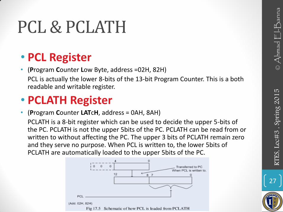
Clock and Instruction Cycles
• Clock from the oscillator enters a microcontroller via OSC1 pin where internal circuit of a microcontroller divides the clock into four even clocks Q1, Q2, Q3 and Q4 which do not overlap.
• These four clocks make up one instruction cycle (also called machine cycle) during which one instruction is executed.
36
RTES
, Lec
#3 , S
prin
g 201
5 ©
Ahm
ad E
l-Ban
na
Clock and Instruction Cycles..
• Execution of instruction starts by calling an instruction that is next in string.
• Instruction is called from program memory on every Q1 and is written in Instruction Register (IR) on Q4.
• Decoding and execution of instruction are done between the next Q1 and Q4 cycles. The following diagram shows the relationship between instruction cycle and clock of the oscillator (OSC1) as well as that of internal clocks Q1 – Q4.
• Program Counter (PC) holds information about the address of the next instruction.
37
RTES
, Lec
#3 , S
prin
g 201
5 ©
Ahm
ad E
l-Ban
na

Pipelining in PIC
• There are 35 single word instructions. A two-stage pipeline overlaps fetch and execution of instructions. As a result, all instructions execute in a single cycle except for program branches. These take two cycles since the fetch instruction is “flushed” from the pipeline while the new instruction is being fetched and then executed.
• A typical picture of the pipeline is shown in Figure 3.
38
RTES
, Lec
#3 , S
prin
g 201
5 ©
Ahm
ad E
l-Ban
na
Figure3: Instruction Pipeline Flow

• For more details, refer to:
• Chapter 14, John Catsoulis, Designing Embedded Hardware, 2005.
• The lecture is available online at:
• http://bu.edu.eg/staff/ahmad.elbanna-courses/12134
• For inquires, send to:
39
© A
hmad
El-B
anna
RT
ES, L
ec#3
, Spr
ing 2
015
Recommended
![Chapter 4 Introduction to Bipolar Junction Transistors (BJTs)bu.edu.eg/portal/uploads/Engineering, Shoubra/Electrical Engineering... · Figure 4.3 Forward-reverse bias of a BJT. [5]](https://img.dokumen.tips/doc/110x75/5ebfec4b97389926ad05ea31/chapter-4-introduction-to-bipolar-junction-transistors-bjtsbueduegportaluploadsengineering.jpg)