Lecture 12: Photodiode detectors
Background concepts p-n photodiodes Photoconductive/photovoltaic modes p-i-n photodiodes Responsivity and bandwidth Noise in photodetectors
1
References: This lecture partially follows the materials from Photonic Devices, Jia-Ming Liu, Chapter 14. Also from Fundamentals of Photonics, 2nd ed., Saleh & Teich, Chapters 18.

2
Electron-hole photogeneration Most modern photodetectors operate on the basis of the
internal photoelectric effect – the photoexcited electrons and holes remain within the material, increasing the electrical conductivity of the material
Electron-hole photogeneration in a semiconductor
h
h
• absorbed photons generate free electron-hole pairs
• Transport of the free electrons and holesupon an electric field results in a current
Eg

3
Absorption coefficient
Bandgaps for some semiconductor photodiode materials at 300 K
Bandgap (eV) at 300 K
Indirect Direct
SiGeGaAsInAsInPGaSbIn0.53Ga0.47AsIn0.14Ga0.86AsGaAs0.88Sb0.12
1.140.67-------
4.100.811.430.351.350.730.751.151.15
kink

4
Absorption coefficient E.g. absorption coefficient = 103 cm-1
Means an 1/e optical power absorption length of
1/ = 10-3 cm = 10 m
Likewise, = 104 cm-1 => 1/e optical power absorption length of 1 m.
= 105 cm-1 => 1/e optical power absorption length of 100 nm.
= 106 cm-1 => 1/e optical power absorption length of 10 nm.

5
Indirect absorption Silicon and germanium absorb light by both indirect and
direct optical transitions. Indirect absorption requires the assistance of a phonon so that
momentum and energy are conserved. Unlike the emission process, the absorption process can be
sequential, with the excited electron-hole pair thermalize within their respective energy bands by releasing energy/momentum via phonons.
This makes the indirect absorption less efficient than direct absorption where no phonon is involved.
electron wavevector k
Electronenergy
h thermalization
Phononprocess

6
Indirect vs. direct absorption in silicon and germanium
Silicon is only weakly absorbing over the wavelength band 0.8 – 0.9 m. This is because transitions over this wavelength band in silicon are due only to the indirectabsorption mechanism. The threshold for indirect absorption (long wavelength cutoff) occurs at 1.09 m.
The bandgap for direct absorption in silicon is 4.10 eV, corresponding to a threshold of 0.3 m.
Germanium is another semiconductor material for which the lowest energy absorption takes place by indirect optical transitions. Indirect absorption will occur up to a threshold of 1.85 m.
However, the threshold for direct absorption occurs at 1.53 m, for shorter wavelengths germanium becomes strongly absorbing (see the kink in the absorption coefficient curve).

7
Choice of photodiode materials A photodiode material should be chosen with a bandgap
energy slightly less than the photon energy corresponding to the longest operating wavelength of the system.
This gives a sufficiently high absorption coefficient to ensure a good response, and yet limits the number of thermally generated carriers in order to attain a low “dark current” (i.e. current generated with no incident light).
Germanium photodiodes have relatively large dark currentsdue to their narrow bandgaps in comparison to other semiconductor materials. This is a major shortcoming with the use of germanium photodiodes, especially at shorter wavelengths (below 1.1 m)
Eg slightly less than hLhL hs

8
III-V compound semiconductors Direct-bandgap III-V compound semiconductors can be
better material choices than germanium for the longer wavelength region.
Their bandgaps can be tailored to the desired wavelength by changing the relative concentrations of their constituents (resulting in lower dark currents).
They may also be fabricated in heterojunction structures (which enhances their high-speed operations).
e.g. In0.53Ga0.47As lattice matched to InP substrates responds to wavelengths up to around 1.7 m. (most important for 1.3 and 1.55 m)

9
Junction photodiodes The semiconductor photodiode detector is a p-n junction
structure that is based on the internal photoeffect.
The photoresponse of a photodiode results from the photogeneration of electron-hole pairs through band-to-band optical absorption.=> The threshold photon energy of a semiconductor photodiode is the bandgap energy Eg of its active region.
The photogenerated electrons and holes in the depletion layerare subject to the local electric field within that layer. The electron/hole carriers drift in opposite directions. This transport process induces an electric current in the external circuit.
Here, we will focus on semiconductor homojunctions.

10
e- diffusionregion
Photoexcitation and energy-band diagram of a p-n photodiode
h h
h
h h
Depletion layer
WLe
homogeneousp region
h+ diffusionregion
Lh
homogeneousn region
drift
drift
diffusion
diffusion
Recombine with majority h+
before reaching the junction
Recombine withmajority e-
before reaching the junctionActive regionp n

11
In the depletion layer, the internal electric field sweeps the photogenerated electron to the n side and the photogenerated hole to the p side.=> a drift current that flows in the reverse direction from the n side (cathode) to the p side (anode).
Within one of the diffusion regions at the edges of the depletion layer, the photogenerated minority carrier (hole in the n side and electron in the p side) can reach the depletion layer by diffusion and then be swept to the other side by the internal field. => a diffusion current that also flows in the reverse direction.
In the p or n homogeneous region, essentially no current is generated because there is essentially no internal field to separate the charges and a minority carrier generated in a homogeneous region cannot diffuse to the depletion layer before recombining with a majority carrier.

12
Photocurrent in an illuminated junction
If a junction of cross-sectional area A is uniformly illuminated by photons with h > Eg, a photogeneration rateG (EHP/cm3-s) gives rise to a photocurrent.
The number of holes created per second within a diffusion length Lh of the depletion region on the n side is ALhG.
The number of electrons created per second within a diffusion length Le of the depletion region on the p side is ALeG.
Similarly, AWG carriers are generated within the depletion region of width W.
The resulting junction photocurrent from n to p:
Ip = eA (Lh + Le + W) G

13
Diode equation Recall the current-voltage (I-V) characteristic of the junction is
given by the diode equation:
I = I0(exp(eV/kBT) – 1)
The current I is the injection current under a forward bias V. I0 is the “saturation current” representing thermal-generated free
carriers which flow through the junction (dark current).
V
I
Dark current

14
I-V characteristics of an illuminated junction The photodiode therefore has an I-V characteristic:
I = I0(exp(eV/kBT) – 1) – Ip
This is the usual I-V curve of a p-n junction with an added photocurrent –Ip proportional to the photon flux.
p
nIp
Ip
Vp
V
I
G = 0
G1
G2
G3
I0
Ip

15
Short-circuit current and open-circuit voltage
The short-circuit current (V = 0) is the photocurrent Ip. The open-circuit voltage (I = 0) is the photovoltage Vp.
Vp = (kBT/e) ln(Ip/I0 + 1)
Ip1
Ip
Ip2
Ip3
Vp
+
-
V
I
G = 0
G1
G2
G3
I0
Vp1 Vp2 Vp3

16
Photocurrent and photovoltage
As the light intensity increases, the short-circuit current increases linearly (Ip G);
The open-circuit voltage increases only logarithmically (Vp ln (Ip/I0)) and limits by the equilibrium contact potential.
Intensity (mW/cm2)
Vp (V)
Ip (A)

17
Open-circuit voltage
The photogenerated, field-separated, majority carriers (+ve charge on the p-side, -ve charge on the n-side) forward-bias the junction.
The appearance of a forward voltage across an illuminated junction (photovoltage) is known as the photovoltaic effect.
The limit on Vp is the equilibrium contact potential V0 as the contact potential is the maximum forward bias that can appear across a junction. (drift current vanishes with Vp = V0)
e(V0-Vp)Ec
Ev
EF
eV0
EFp
EFneVp
+++
---
p n p n
Accumulatedmajoritycarriers
Accumulated majoritycarriers
e(V0-Vp)
18
Photoconductive and photovoltaic modes There are two modes of operation for a junction photodiode:
photoconductive and photovoltaic
The device functions in photoconductive mode in the thirdquadrant of its current-voltage characteristics, including the short-circuit condition on the vertical axis for V = 0. (acting as a current source)
It functions in photovoltaic mode in the fourth quadrant, including the open-circuit condition on the horizontal axis for I = 0. (acting as a voltage source with output voltage limited by the equilibrium contact potential)
The mode of operation is determined by the bias conditionand the external circuitry.

19
Photoconductive mode under reverse bias
Ec
Ev
EF
eV0
p n
Ec
Ev
EFpe(V0 + VB)
p n
EFn
eVB
(For silicon photodiodes, V0 0.7 V, VB can be up to -5 – -10 V)
W W+D

20
Basic circuitry and load line for the photoconductive mode
“Photoconductive” mode – reverse biasing the photodiode With a series load resistor RL< Ri gives the load line Keep Vout < VB so that the photodiode is reverse biased
(VB is sufficiently large) Under these conditions and before it saturates, a photodiode has the following
linear response: Vout = (I0 + Ip) RL
Vout
+
-
RLVB
Ri
V
I
G = 0
G1
-VB
-VB/RL
RL << Ri
I0
Vout = 0V
+
-
VBRi
V
I
G = 0
G1
-VBI0
RL = 0
I0+Ip I0+Ip
Vout
(short-circuit current)

21
Basic circuitry and load line for the photovoltaic mode
Vout
+
-V
I
G = 0
G1
G2
G3
I0
RL
RL >> Ri
I
• Does not require a bias voltage but requires a large load resistance.
• RL >> Ri, so that the current I flowing through the diode and the load resistance is negligibly small.
Limited by the contact potential

22
Operation regimes of an illuminated junction
Photoconductive: Power (+ve) is delivered to the device by the external circuit (photodetector)
Photovoltaic: Power (-ve) is delivered to the load by the device(solar cell/ energy harvesting)
3rd quadrant (external reverse bias, reverse current)
V
Ip
nir
+
-Vr
RL
4th quadrant(internal forward bias, reverse current)
V
Ip
nir
-
+V
RL

23
A reverse-biased p-n photodiode
It is important that the photons are absorbed in the depletion region. Thus, it is made as long as possible (say by decreasing the doping in the n type material). The depletion region width in a p-n photodiode is normally 1 – 3 m.
The depletion-layer width widens and the junction capacitance drops with reverse voltage across the junction.
p
n
E-field
Depletion region
Diffusion region
Absorptionregion
W + D

24
p-i-n photodiodes
A p-i-n photodiode consists of an intrinsic region sandwiched between heavily doped p+ and n+
regions. The depletion layer is almost completely defined by the intrinsic region.
In practice, the intrinsic region does not have to be truly intrinsic but only has to be highly resistive (lightly doped p or n region).

25
A reverse-biased p-i-n photodiode
All the absorption takes place in the depletion region. The intrinsic region can be an n-type material that is lightly doped, and to make a low-resistance contact a highly doped n-type (n+) layer is added.
p
i
E-field
Depletion region
Absorption region
n+
||
26
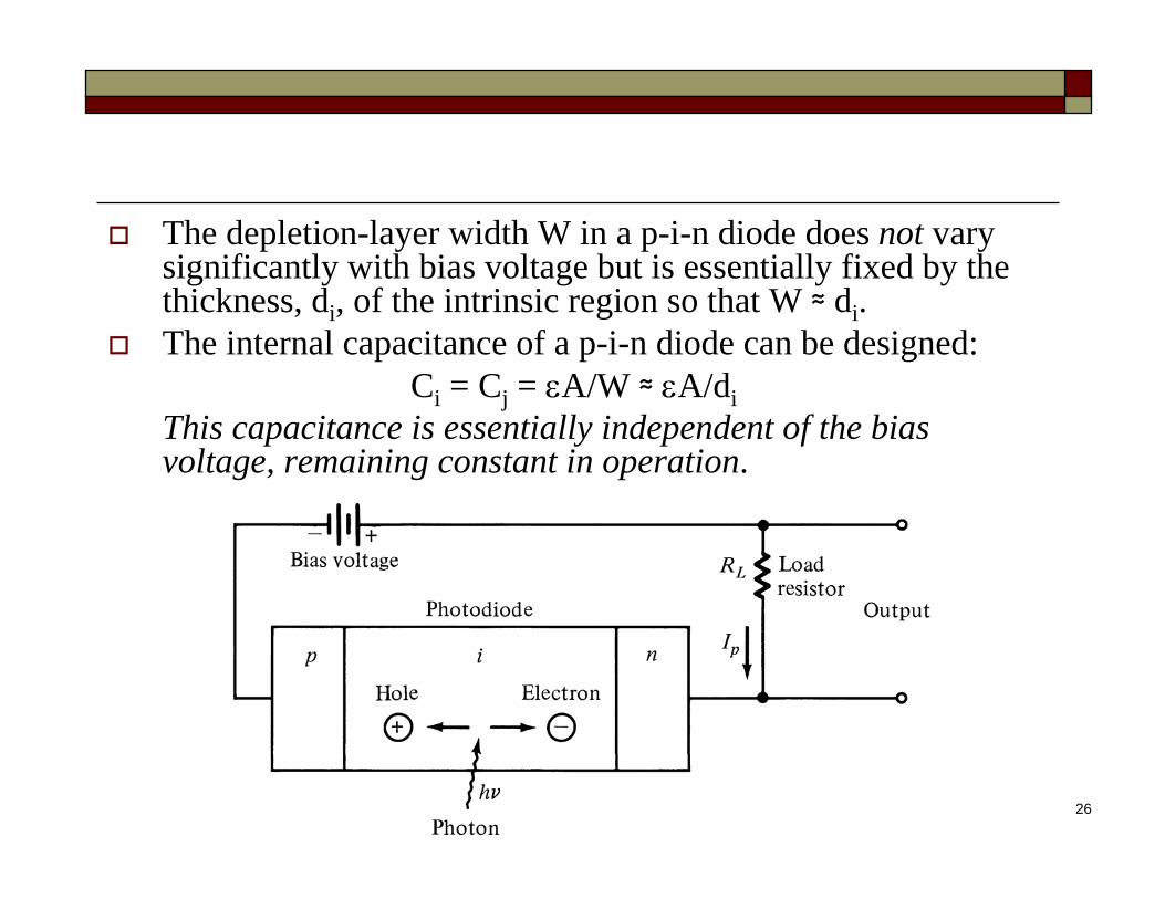
The depletion-layer width W in a p-i-n diode does not vary significantly with bias voltage but is essentially fixed by the thickness, di, of the intrinsic region so that W ≈ di.
The internal capacitance of a p-i-n diode can be designed:Ci = Cj = A/W ≈ A/di
This capacitance is essentially independent of the bias voltage, remaining constant in operation.

27
p-i-n photodiodes offer the following advantages: Increasing the width of the depletion layer (where the
generated carriers can be transported by drift) increases the area available for capturing light
Increasing the width of the depletion layer reduces the junction capacitance and thereby the RC time constant. Yet, the transit time increases with the width of the depletion layer.
Reducing the ratio between the diffusion length and the drift length of the device results in a greater proportion of the generated current being carried by the faster drift process.

28
Heterojunction photodiodes Many III-V p-i-n photodiodes have heterojunction
structures. Examples: p+-AlGaAs/GaAs/n+-AlGaAs, p+-InP/InGaAs/n+-
InP, or p+-AlGaAs/GaAs/n+-GaAs, p+-InGaAs/InGaAs/n+-InP.
AlGaAs/GaAs (0.7 – 0.87 m) InGaAs/InP (1300 – 1600 nm). A typical InGaAs p-i-n
photodetector operating at 1550 nm has a quantum efficiency ≈ 0.75 and a responsivity R ≈ 0.9 A/W
p+ InP
i InGaAs
n+ InP
P
narrow bandgap
wide bandgap
wide bandgap

29
Heterojunction photodiodes Heterojunction structures offer additional flexibility in
optimizing the performance of a photodiode. In a heterojunction photodiode, the active region normally
has a bandgap that is smaller than one or both of the homogeneous regions.
A wide-bandgap homogeneous region, which can be either the top p+ region or the substrate n region, serves as a windowfor the optical signal to enter.
The small bandgap of the active region determines the long-wavelength cutoff of the photoresponse, th.
The large bandgap of the homogeneous window region sets the short-wavelength cutoff of the photoresponse, c.
=> For an optical signal that has a wavelength s in the range th> s > c, the quantum efficiency and the responsivity can be optimized.

30
InGaAs fiber-optic pin photodetector(Thorlabs D400FC) Spectral response 800 – 1700 nm
Peak response 0.95 A/W @ 1550 nm
Rise/fall time 0.1 ns
Diode capacitance 0.7 pF (typ)
NEP @ 1550 nm 1.0 x 10⁻¹⁵ W/Hz
Dark current 0.7nA (typ),1.0nA (max)
PD Active diameter 0.1 mm
Bandwidth 1 GHz (min)
Damage threshold 100 mW CW
Bias (reverse) 12V battery
Coupling lens 0.8” dia. Ball lens
Coupling efficiency 92% (typ) from both single- and multi-mode fibers over full spectral response
fiber RF cable
Light in
c th

31
Application notes – output voltage
The RF output signal (suitable for both pulsed and CW light sources) is the direct photocurrent out of the photodiode anode and is a function of the incident light power and wavelength.
The responsivity R() can be used to estimate the amount of photocurrent.
To convert this photocurrent to a voltage (say for viewing on an oscilloscope), add an external load resistance, RL.
The output voltage is given as:
V0 = P R() RL

32
Responsivity
The responsivity of a photodetector relates the electric current Ip flowing in the device circuit to the optical power P incident on it.
Ip = e = eP/h R P : quantum efficiency
Responsivity R = Ip/P = e/h = /1.24 [A/W]
(Recall the LED responsivity [W/A])
The responsivity is linearly proportional to both the quantum efficiency and the free-space wavelength .(e.g. for = 1, = 1.24 m, R = 1 A/W)
33
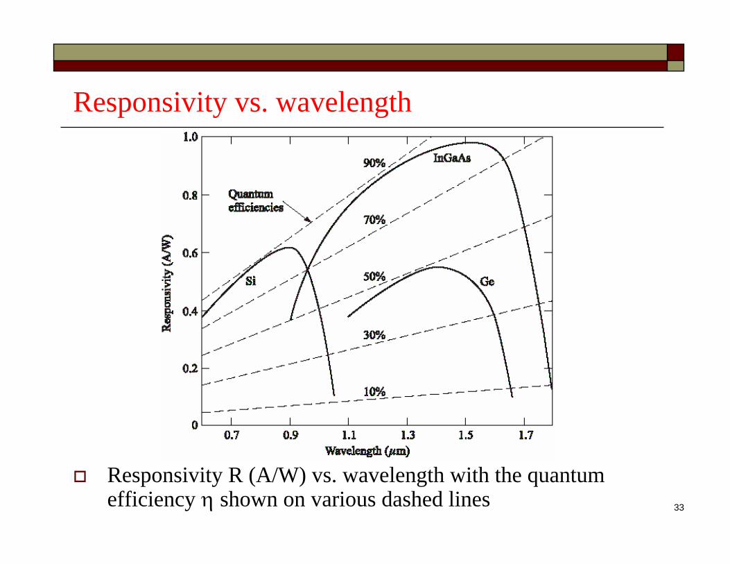
Responsivity vs. wavelength
Responsivity R (A/W) vs. wavelength with the quantum efficiency shown on various dashed lines

34
Quantum efficiency The quantum efficiency (external quantum efficiency) of a
photodetector is the probability that a single photon incident on the device generates a photocarrier pair that contributes to the detector current.
= (1-R) [1 – exp(-d)]
R is the optical power reflectance at the surface, is the fraction of electron-hole pairs that contribute to the detector current, the absorption coefficient of the material, and d the photodetector depth.
is the fraction of electron-hole pairs that avoid recombination (often dominated at the material surface) and contribute to the useful photocurrent. Surface recombination can be reduced by careful material growth and device design/fabrication.
[1 – exp(-d)] represents the fraction of the photon flux absorbed in the bulk of the material. The device should have a value of d that is sufficiently large. (d > 1/ = 104 cm-1, d > 1 m)

35
Dependence of quantum efficiency on wavelengths The characteristics of the semiconductor material determines
the spectral window for large . The bandgap wavelength g = hc/Eg is the long-wavelength
limit of the semiconductor material. For sufficiently short , also decreases because most
photons are absorbed near the surface of the device (e.g. for = 104 cm-1, most of the light is absorbed within a distance 1/ = 1 m; for = 105 – 106 cm-1, most of the light is absorbed within a distance 1/ = 0.1 – 0.01 m).
The recombination lifetime is quite short near the surface, so that the photocarriers recombine before being collected. (short-wavelength limit)
In the near-infrared region, silicon photodiodes with antireflection coating can reach 100% quantum efficiency near 0.8 – 0.9 m.
In the 1.0 – 1.6 m region, Ge photodiodes, InGaAs photodiodes, and InGaAsP photodiodes have shown high quantum efficiencies.

36
Application notes - bandwidth The bandwidth, f3dB, and the 10 - 90% rise-time response, tr,
are determined from the diode capacitance Cj, and the load resistance RL:
f3dB = 1/(2 RLCj)
tr = 0.35/f3dB
For maximum bandwidth, use a direct connection to the measurement device having a 50 input impedance. An SMA-SMA RF cable with a 50 terminating resistor at the end can also be used. This will minimize ringing by matching the coax with its characteristic impedance.
If bandwidth is not important, such as for continuous wave (CW) measurement, one can increase the amount of voltage for a given input light by increasing the RL up to a maximum value (say 10 k).

37
Speed-limiting factors of a photodiode
High-speed photodiodes are by far the most widely used photodetectors in applications requiring high-speed or broadband photodetection.
The speed of a photodiode is determined by two factors: The response time of the photocurrent The RC time constant of its equivalent circuit
Because a photodiode operating in photovoltaic mode has a large RC time constant due to the large internal diffusion capacitance upon internal forward bias in this mode of operation => only photodiodes operating in a photoconductive mode are suitable for high-speed or broadband applications.

38
Response time of the photocurrent (photoconductive mode)
The response time is determined by two factors: Drift of the electrons and holes that are photogenerated in the
depletion layer Diffusion of the electrons and holes that are photogenerated in
the diffusion regions Drift of the carriers across the depletion layer is a fast process -
given by the transit times of the photogenerated electrons and holes across the depletion layer.
Diffusion of the carriers is a slow process – caused by the optical absorption in the diffusion regions outside of the high-field depletion region. (diffusion current can last as long as the carrier lifetime)=> a long tail in the impulse response of the photodiode=> a low-frequency falloff in the device frequency response

39
Drift velocity and carrier mobility A constant electric field E presented to a semiconductor (or
metal) causes its free charge carriers to accelerate. The accelerated free carriers then encounter frequent
collisions with lattice ions moving about their equilibrium positions via thermal motion and imperfections in the crystal lattice (e.g. associated with impurity ions).
These collisions cause the carriers to suffer random decelerations (like frictional force!)=> the result is motion at an average velocity rather than at a constant acceleration.
The mean drift velocity of a carrier
vd = (eE/m) col = E
where m is the effective mass, col is the mean time between collisions, = ecol/m is the carrier mobility.

40
Drift time upon saturated carrier velocities
When the field in the depletion region exceeds a saturationvalue then the carriers travel at a maximum drift velocity vd.
The longest transit time tr is for carriers which must traverse the full depletion layer width W:
tr = W/vd
A field strength above 2 x 10⁴ Vcm-1 (say 2 V across 1 m distance) in silicon gives maximum (saturated) carrier velocities of approximately 107 cms-1. (max. vd)
=> The transit time through a depletion layer width of 1 m is around 10 ps.

41
Diffusion time Diffusion time of carriers generated outside the depletion
region – carrier diffusion is a relatively slow process. The diffusion time, diff, for carriers to diffuse a distance d is
diff = d2/2D
where D is the minority carrier diffusion coefficient.
e.g. The hole diffusion time through 10 m of silicon is 40 ns. The electron diffusion time over a similar distance is around 8 ns.=> for a high-speed photodiode, this diffusion mechanism has to be eliminated (by reducing the photogeneration of carriers outside the depletion layer through design of the device structure, say using heterojunction pin diode).

42
Photodiode capacitance Time constant incurred by the capacitance of the
photodiode with its load – the junction capacitance
Cj = A/W
where is the permittivity of the semiconductor material and A is the diode junction area.
A small depletion layer width W increases the junction capacitance.
(The capacitance of the photodiode Cpd is that of the junctiontogether with the capacitance of the leads and packaging. This capacitance must be minimized in order to reduce the RC time constant. In ideal cases, Cpd ≈ Cj.)

43
Remarks on junction capacitance For pn junctions, because the width of the depletion layer
decreases with forward bias but increases with reverse bias, the junction capacitance increases when the junction is subject to a forward bias voltage but decreases when it is subject to a reverse bias voltage.
For p-i-n diodes, the width of the depletion (intrinsic) layer is fixed => the junction capacitance is not affected by biasing conditions.
e.g. A GaAs p-n homojunction has a 100 m x 100 m cross section and a width of the depletion layer W = 440 nm. Consider the junction in thermal equilibrium without bias at 300 K. Find the junction capacitance.
= 13.180 for GaAs, 0 = 8.854 x 10⁻¹² Fm-1
Cj = 13.18 x 8.854 x 10-12 x 1 x 10-8/(440 x 10-9) = 2.65 pF

44
Photodiode response to rectangular optical input pulses for various detector parameters
(b) W >> 1/ (all photons are absorbed in the depletion layer) and small Cj.
(c) W >> 1/, large photodiode capacitance, RC time limited(d) W 1/some photons are absorbed in the diffusion region
diffusion component limited
(optical) High-speedphotodiode response
Distortedwaveform
Distortedwaveform
45
Transit-time-limited Thus, for a high-speed photodiode, diffusion mechanism has
to be eliminated (by reducing the photogeneration of carriers outside the depletion layer through design of the device structure).
When the diffusion mechanism is eliminated, the frequency response of the photocurrent is only limited by the transit times of electrons and holes.
In a semiconductor, electrons normally have a higher mobility (smaller electron effective mass), thus a smaller transit time, than holes.
For a good estimate of the detector frequency response, we use the average of electron and hole transit times:
tr = ½(tre + tr
h)

46
Approximated transit-time-limited power spectrum In the simple case when the process of carrier drift is
dominated by a constant transit time of tr
=> the temporal response of the photocurrent is ideally a rectangular function of duration tr in the time domain
=> the power spectrum of the photocurrent frequency response can be approximately given as a sinc function in the frequency domain:
Rph2(f) = |iph(f)/P(f)|2 ≈ Rph
2(0) (sin(ftr)/ftr)2
=>a transit-time-limited 3-dB frequency:
fph,3dB ≈ 0.443/tr

47
Total frequency response
0
0.5
1
0 2 4 6 8 10
Rc = 10 psRc = 50 psRc = 100 ps
tr = 50 ps
f3dB = 8.86 GHz≈ 0.443/50ps
Signal frequency f (GHz)
Nor
mal
ized
resp
onse
R2 (
f)/R
2 (0)
Photocurrent power spectrum

48
Small-signal equivalent circuits
• A photodiode has an internal resistance Ri and an internal capacitance Ciacross its junction.
• The series resistance Rs takes into account both resistance in the homogeneous regions of the diode and parasitic resistance from the contacts.
• The external parallel capacitance Cp is the parasitic capacitance from the contacts and the package.
• The series inductance Ls is the parasitic inductance from the wire or transmission-line connections.
• The values of Rs, Cp, and Ls can be minimized with careful design, processing, and packaging of the device.
ipRi Ci
RsLs
Cp RL Vout
+
-

49
Both Ri and Ci depend on the size and the structure of the photodiode and vary with the voltage across the junction.
In photoconductive mode under a reverse voltage, the diode has a large Ri normally on the order of 1 – 100 M for a typical photodiode, and a small Ci dominated by the junction capacitance Cj.
As the reverse voltage increases in magnitude, Ri increases but Ci decreases because the depletion-layer width increases with reverse voltage.
In photovoltaic mode with a forward voltage across the junction, the diode has a large Ci dominated by the diffusion capacitance Cd.
It still has a large Ri, though smaller than that in the photoconductive mode.

50
Remark on diffusion capacitance
Because the diffusion capacitance is associated with the storage of majority carrier charges in the diffusion region (photogenerated electrons and holes swept from the depletion region stored in the n side and the p side), it exists only when a junction is under forward bias.
When a junction is under forward bias, Cd can be significantly larger than Cj at high injection currents.
When a junction is under reverse bias, Cj is the only capacitance of significance.
=> the capacitance of a junction under reverse bias can be substantially smaller than when it is under forward bias.

51
Frequency response of the equivalent circuit
The frequency response of the equivalent circuit is determined by The internal resistance Ri and capacitance Ci of the
photodiode The parasitic effects characterized by Rs, Cp, and LS The load resistance RL
The parasitic effects must be eliminated as much as possible.
A high-speed photodiode normally operates under the condition that Ri >> RL, Rs. => equivalent resistance ≈ RL
In the simple case, when the parasitic inductance/capacitance are negligible, the speed of the circuit is dictated by the RC time constant RC = RLCi.

52
Approximated power spectrum
The equivalent circuit frequency response:
Rc2(f) ≈ Rc
2(0)/(1 + 42f2RC2)
An RC-time-limited 3-dB frequency
fc,3dB ≈ 1/2RC = 1/2RLCi
Combining the photocurrent response and the circuit response, the total output power spectrum of an optimized photodiode operating in photoconductive mode
R2(f) = Rc2(f) Rph
2(f) ≈ [Rc2(0)/(1+42f2RC
2)] (sin(ftr)/ftr)2

53
RC-time-limited bandwidthe.g. In a silicon photodiode with W = 1 m driven at saturation drift velocity,
tr ≈ 10-4 cm/107 cms-1 ≈ 10 ps
suppose the diode capacitance = 1 pF and a load resistance of 50 ,
RC ≈ 50 ps
=> f3dB ≈ 1/2RC ≈ 3.2 GHz

54
Rise and fall times upon a square-pulse signal
In the time domain, the speed of a photodetector is characterized by the risetime, r, and the falltime, f, of its response to a square-pulse signal.
The risetime - the time interval for the response to rise from 10 to 90% of its peak value.
The falltime - the time interval for the response to decay from 90 to 10% of its peak value.
The risetime of the square-pulse response is determined by the RC circuit-limited bandwidth of the photodetector.

55
Rise time and the circuit 3-dB bandwidth
• Typical response of a photodetector to a square-pulse signal=> the 3-dB bandwidth (for the RC circuit) is
r = 0.35/f3dB

56
For a voltage step input of amplitude V, the output voltage waveform Vout(t) as a function of time t is:
Vout(t) = V[1 – exp(-t/RC)]
=> the 10 to 90% rise time r for the circuit is given by:
r = 2.2 RC
The transfer function for this circuit is given by
|H()| = 1/[1 + 2(RC)2]1/2
The 3-dB bandwidth for the circuit is
f3dB = 1/2RC
=> r = 2.2/2f3dB = 0.35/f3dB

Noise in photodetectors

Noise sources and disturbances
Photon noise – the most fundamental source of noise is associated with the randomarrivals of the photons (usually described by Poisson statistics)Photoelectron noise – a single photon generates an electron-hole pair with probability . The photocarrier-generation process is random.Gain noise – the amplification process that provides internal gain in certain photodetectors is stochastic.Receiver circuit noise – various components in the electrical circuitry of an optical receiver, such as thermal noise in resistors.

Performance measures
The signal-to-noise ratio (SNR) of a random variable - the ratio of its square-mean to its variance. Thus, the SNR of the current i is SNR = i2/i
2, while the SNR of the photon number is SNR = n2/n2
The minimum-detectable signal – the mean signal that yields SNR = 1
The bit error rate (BER) – the probability of error per bit in a digital optical receiver.
The receiver sensitivity – the signal that corresponds to a prescribed value of the SNR. While the minimum-detectable signal corresponds to a receiver sensitivity that provides SNR = 1, a higher value of SNR is often specified to ensure a given value of accuracy (e.g. SNR = 10 – 103 corresponding to 10 – 30 dB). For a digital system, the receiver sensitivity is defined as the minimum optical energy or corresponding mean number of photons per bit required to attain a prescribed BER (e.g. BER = 10-9 or better).
Photon noise• The photon flux associated with a fixed optical power P is
inherently uncertain (statistical).
• The mean photon flux is = P/h, but this quantity fluctuates randomly in accordance with a probability law that depends on the nature of the light source.
• The number of photons n counted in a time interval T is thus random with mean n = T.
• For monochromatic coherent radiation, the photon number statistics obeys the Poisson probability distribution n
2 = n(i.e. variance equals mean)
=> the fluctuations associated with an average of 100 photons result in an actual number of photons that lies approximately within the range 100 10.
Poisson distribution The statistics arriving at a detector follows a discrete
probability distribution which is independent of the number of photons previously detected.
The probability P(z) of detecting z photons in time period when it is expected on average to detect zm photons obeys the Poisson distribution
P(z) = zmz exp(-zm)/z!
where zm the mean is equal to the variance of the probability distribution.
The number of electrons generated in time is equal to the average number of photons detected over this time period
zm = P/h
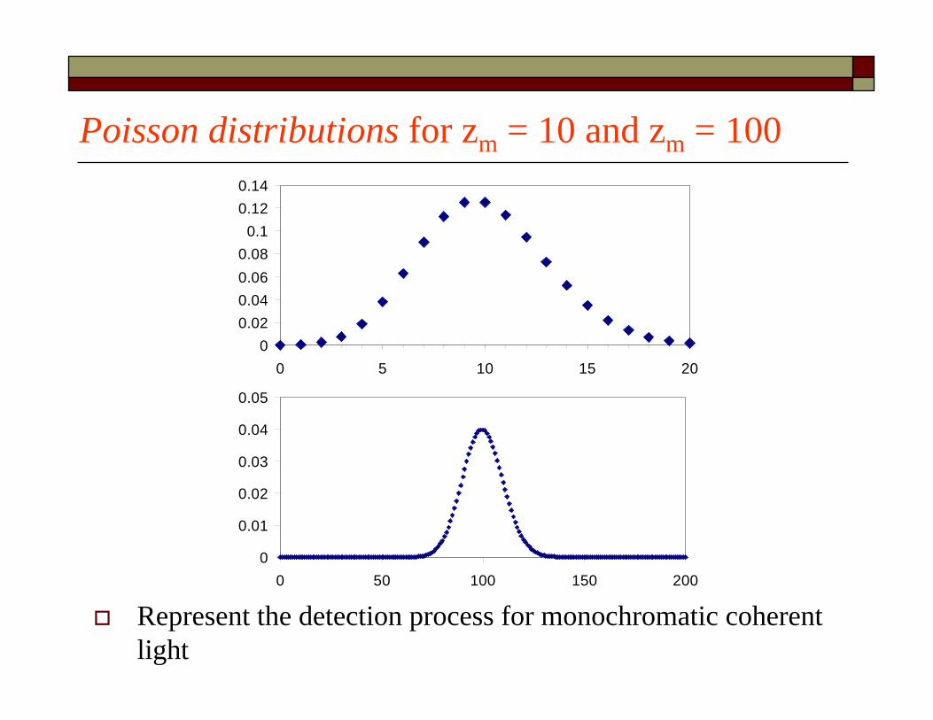
Poisson distributions for zm = 10 and zm = 100
Represent the detection process for monochromatic coherent light
0
0.01
0.02
0.03
0.04
0.05
0 50 100 150 200
00.020.040.060.08
0.10.120.14
0 5 10 15 20

Incoherent light is emitted by independent atoms and therefore there is no phase relationship among the emitted photons. This property dictates exponential distribution for incoherent light (if averaged over the Poisson distribution)
P(z) = zmz/(1 + zm)z+1
This is identical to the Bose-Einstein distribution which is used to describe the random statistics of light emitted in black body radiation (thermal light).
0
0.05
0.1
0 5 10 15 200
0.005
0.01
0 50 100 150
zm = 10 zm = 100
z z

Photon-number signal-to-noise ratio The photon-number signal-to-noise ratio
SNR = n2/n2 = n
and the minimum-detectable photon number
n = 1 photon
If the observation time T = 1 s and the wavelength = 1.24 m, this is equivalent to a minimum detectable power of 0.16 pW. (e = 1.6 x 10⁻¹⁹ C)
The receiver sensitivity for SNR = 103 (30 dB) is 1000 photons. If the time interval T = 10 ns, this is equivalent to a sensitivity of 1011 photons/s or an optical power sensitivity of 16 nW at = 1.24 m.

Photoelectron noise
A photon incident on a photodetector of quantum efficiency generates an electron-hole pair or liberates a photoelectron with probability .
An incident mean photon flux (photons/s) therefore results in a mean photoelectron flux .
The number of photoelectrons m detected in the time interval T is a random variable with mean
m = T = n
If the photon number follows the Poisson probability distribution, so is the photoelectron number.
=> the photoelectron-number variance m2 = m = n

Photoelectron-number signal-to-noise ratio
SNR = m = n
The minimum-detectable photoelectron number is m = n = 1 photoelectron, corresponding to 1/photons (i.e. > 1 photons).
The receiver sensitivity for SNR = 103 is 1000 photoelectrons or 1000/ photons.

Photocurrent noise
Here we examine the properties of the electric current i(t) induced in a circuit by a random photoelectron flux with mean .
We include the effects of photon noise, photoelectron noise, and the characteristic time response of the detector and circuitry (filtering).
Assume every photoelectron-hole pair generates a pulse of electric current with charge (area) e and time duration p in the external circuit of the photodetector.
A photon stream incident on a photodetector therefore results in a stream of current pulses which add together to constitute the photocurrent i(t).=> The randomness of the photon stream is transformed into a fluctuating electric current. If the incident photons are Poisson distributed, these fluctuations are known as shot noise.

Shot noise
The photocurrent induced in a photodetector circuit comprises a superposition of current pulses, each associated with a detected photon. The individual pulses illustrated are exponentially decaying step functions but they can assume an arbitrary shape.
photons
photoelectrons
Current pulses
Electric current(shot noise) i(t)
t
t
t
ti(t)
Area etp

Consider a photon flux incident on a photoelectric detector of quantum efficiency .
Let the random number m of photoelectrons counted within a characteristic time interval T = 1/2B (the resolution time of the circuit) generate a photocurrent i(t), where t is the instant of time immediately following the interval T. (The parameter B represents the bandwidth of the device/circuit system.)
For rectangular current pulses of duration T, the current and photoelectron-number random variables are related by i = (e/T) m.
The photocurrent mean and variance are
i = (e/T) m
i2 = (e/T)2 m
2
where m = T = /2B is the mean number of photoelectrons collected in the time interval T = 1/2B.

Substituting m2 = m for the Poisson law yields the
photocurrent mean and variance
i = ei
2 = 2e B i
=> the photocurrent SNR
SNR = i2/i2 = i/2eB = /2B = m
The current SNR is directly proportional to the photon flux and inversely proportional to the electrical bandwidth of the circuit B.
The result is identical to that of the photoelectron-number SNR ratio m as expected as the circuit introduces no added randomness.

e.g. SNR and receiver sensitivity. For i = 10 nA and the electrical bandwidth of the circuit B = 100 MHz, i ≈ 0.57 nA, corresponding to a SNR = 310 or 25 dB. => An average of 310 photoelectrons are detected in every time interval T = 1/2B = 5 ns.=> The minimum-detectable photon flux for SNR = 1 is
= 2B/=> The receiver sensitivity for SNR = 103 is
= 1000 (2B/) = 2 x 10¹¹/ photons/s

Dark current noise When there is no optical power incident on the photodetector
a small reverse leakage current still flows from the device terminals.
Dark-current noise results from random electron-hole pairs generated thermally (or by tunneling).
This dark current contributes to the total system noise and gives random fluctuations about the average photocurrent. => It therefore manifests itself as shot noise on the photocurrent.
The dark current noise is
d2 = 2 eB Id

Thermal noise Thermal noise (also called Johnson noise or Nyquist noise)
results from random thermal motions of the electrons in a conductor. It is associated with the blackbody radiation of a conductor at the radio or microwave frequency range of the signal.
Because only materials that can absorb and dissipate energycan emit blackbody radiation, thermal noise is generated only by the resistive components of the detector and its circuit. (Capacitive and inductive components do not generate thermal noise because they neither dissipate nor emit energy.)
These motions give rise to a random electric current even in the absence of an external electrical power source. The thermal electric current in a resistance R is a random function i(t) whose mean value i(t) = 0.
=> the variance of the current i2 = Ith
2

In normal operation of most photodetectors, f << kBT/h = 6.24 THz at room temperature, the frequency dependence of the thermal noise power is negligible
The total thermal noise power for a detection system of a bandwidth B is
Pn,th = 4kBTB
For a resistor that has a resistance R, the thermal noise can be treated as either current noise or voltage noise
Pn,th = Ith2 R = vth
2/R
=> Ith2 = 4kBTB/R and vth
2 = 4kBTBR
e.g. A 1-k resistor at T = 300o K in a circuit bandwidth B = 100 MHz exhibits an RMS thermal noise current Ith
21/2 ≈ 41 nA.

For an optical detection system, the resistance R is the total equivalent resistance, including the internal resistance of the detector and the load resistance RL from the circuit, at the output of the detector.
For a detector that has a current signal, the thermal noise is determined by the lowest shunt resistance to the detector, which is often the load resistance of the detector. => The thermal current noise Ith
2 = 4kBTB/RL can be reduced by increasing this resistance at the expense of reducing the response speed of the system.
For a detector that has a voltage signal, the thermal voltage noise vth
2 = 4kBTBRL can be reduced by decreasing this resistance, but at the expense of reducing the output voltage signal.

Signal-to-noise ratio The total noise of a photodetector is basically the sum of its
shot noise and thermal noise:
n2 = sh
2 + th2
A photodetector is said to function in the quantum regime if sh
2 > th2 (shot-noise limited)
A photodetector is in the thermal regime if th2 > sh
2
(thermal-noise limited)
SNR = Ip2/n2 = Ip2/[2eB(Ip + Id) + 4kBTB/RL]
= P2R2/[2eB(PR + Id) + 4kBTB/RL]
where R = e/h is the responsivity of a photodetector.

Noise equivalent power The NEP of a photodetector is defined as the input power
required of the optical signal for the signal-to-noise ratio to be unity, SNR = 1, at the detector output.
The NEP for a photodetector that has an output current signal can be defined as
NEP = in21/2/R
where in2 is the mean square noise current at an input
optical power level for SNR = 1 and R is the responsivity.
For most detection systems at the small input signal level for SNR = 1, the shot noise contributed by the input optical signal is negligible compared to both the shot noise from other sources and the thermal noise of the detector.

In this situation, the NEP of a photodetector:
NEP = (2eid + 4kBT/RL)1/2 B1/2 / R
The NEP of a photodetector is often specified in terms of the NEP for a bandwidth of 1 Hz as NEP/B1/2, in the unit of W Hz-1/2.
In order to reduce the RC time constant, a high-speed photodetector that has a current signal normally has a small area, thus a small dark current, but requires a small load resistance, thus a large thermal noise.
=> the NEP of a high-speed photodetector is usually limited by the thermal noise from its external load resistance (4kBTB/RL) rather than by the shot noise from its internal dark current (2eB id).

E.g. A Si photodetector has an active area of A = 5 mm2, a bandwidth of B = 100 MHz, and a dark current of id = 10 nA. Find its shot-noise limited NEP, its thermal-noise-limited NEP, and its total NEP, all for a bandwidth of 1 Hz. Calculate the total NEP for its entire bandwidth.
The shot noise from the dark currentish
2 = 2eB id = 2 x 1.6 x 10-19 x 10 x 10-9 x B A2 Hz-1
= 3.2 x 10⁻²⁷ B A2 Hz-1
The thermal noiseith
2 = 4kBTB/RL= (4 x 25.9 x 10-3 x 1.6 x 10-19 / 50) x B A2 Hz-1
= 3.32 x 10⁻²² B A2 Hz-1
The total noise in2 = ish
2 + ith2 = 3.32 x 10⁻²² B A2 Hz-1, which is completely
dominated by thermal noise.
Suppose R = 0.5 AW-1. The shot-noise-limited NEP for a bandwidth of 1 Hz:
(NEP)sh/B1/2 = ish21/2/(B1/2R) = 113 fW Hz-1/2

The thermal-noise-limited NEP for a bandwidth of 1 Hz is
(NEP)th/B1/2 = ith21/2/(B1/2R) = 36.4 pW Hz-1/2
The total NEP for a bandwidth of 1 Hz is
NEP/B1/2 = 36.4 pW Hz-1/2
For B = 100 MHz, the total NEP for the entire bandwidth is
NEP = 36.4 x 10-12 x (100 x 106)1/2 W = 364 nW
This detector is completely limited by the thermal noise of its load resistance.
Recommended


