1
DEPARTMENT OF ELECTRICAL AND ELECTRONICSENGINEERING
EE6211-ELECTRIC CIRCUITS LABORATORY
LABORATORY MANUAL
1ST YEAR – EEE
(REGULATION 2013)

EE6211 - Electric Circuits Laboratory
2
EE6211 ELECTRIC CIRCUITS LABORATORY L T P C 0 0 3 2
LIST OF EXPERIMENTS
1. Experimental verification of Kirchhoff’s voltage and current laws2. Experimental verification of network theorems (Thevenin, Norton, Superposition
and maximum power transfer Theorem).3. Study of CRO and measurement of sinusoidal voltage, frequency and power factor.4. Experimental determination of time constant of series R-C electric circuits.5. Experimental determination of frequency response of RLC circuits.6. Design and Simulation of series resonance circuit.7. Design and Simulation of parallel resonant circuits.8. Simulation of low pass and high pass passive filters.9. Simulation of three phase balanced and unbalanced star, delta networks circuits.10. Experimental determination of power in three phase circuits by two-watt meter
method.11. Calibration of single phase energy meter.12. Determination of two port network parameters.
TOTAL: 45 PERIODS
LABORATORY REQUIREMENTS FOR BATCH OF 30 STUDENTS
1 Regulated Power Supply: 0 – 15 V D.C - 10 Nos / Distributed Power Source.2 Function Generator (1 MHz) - 10 Nos.3 Single Phase Energy Meter - 1 No.4 Oscilloscope (20 MHz) - 10 Nos.5 Digital Storage Oscilloscope (20 MHz) – 1 No.6 Circuit Simulation Software (5 Users) (Pspice / Matlab /other Equivalent softwarePackage) with PC (5 Nos.) and Printer (1 No.)7 AC/DC - Voltmeters (10 Nos.), Ammeters (10 Nos.) and Multi-meters (10 Nos.)8 Single Phase Wattmeter – 3 Nos.9 Decade Resistance Box, Decade Inductance Box, Decade Capacitance Box Each - 6Nos.10 Circuit Connection Boards - 10 Nos.Necessary Quantities of Resistors, Inductors, Capacitors of various capacities (QuarterWatt to 10 Watt)

EE6211 - Electric Circuits Laboratory
3
EE6211 ELECTRIC CIRCUITS LABORATORY
Cycle – 1
1. Experimental verification of Kirchhoff’s voltage and current laws.
2. Experimental verification of network theorems (Thevenin, Norton, Superposition
and maximum power transfer Theorem).
3. Study of CRO and measurement of sinusoidal voltage, frequency and power
factor.
4. Design and Simulation of series resonance circuit.
5. Design and Simulation of parallel resonant circuits.
6. Simulation of low pass and high pass passive filters.
Cycle – 2
1. Simulation of three phase balanced and unbalanced star, delta networks circuits.
2. Experimental determination of power in three phase circuits by two-watt meter
method.
3. Calibration of single phase energy meter.
4. Determination of two port network parameters.
5. Experimental determination of time constant of series R-C electric circuits.
6. Experimental determination of frequency response of RLC circuits.
ADDITIONAL EXPERIMENTS:
1. Verification of Compensation Theorem.
2. Verification of Reciprocity Theorem.

EE6211 - Electric Circuits Laboratory
4
Sl.No. DATE TITLE OF THE EXPERIMENT MARKS SIGN
1Experimental verification of Kirchhoff’svoltage and current laws.
2
Experimental verification of networktheorems (Thevenin, Norton,Superposition and maximum powertransfer Theorem).
3Study of CRO and measurement ofsinusoidal voltage, frequency and powerfactor.
4Design and Simulation of seriesresonance circuit.
5 Design and Simulation of parallelresonant circuits.
6 Simulation of low pass and high passpassive filters.
7 Simulation of three phase balanced andunbalanced star, delta networks circuits.
8 Experimental determination of power inthree phase circuits by two-watt metermethod.
9Calibration of single phase energy meter.
10 Determination of two port networkparameters.
11 Experimental determination of timeconstant of series R-C electric circuits.
12 Experimental determination of frequencyresponse of RLC circuits.

EE6211 - Electric Circuits Laboratory
5
CIRCUIT DIAGRAM FOR KIRCHHOFF’S CURRENT LAW
Fuse Calculation:
125% of Rated Current = 1.25 * 21mA = 26.25mA
OBSERVATION TABLE
S.No V
(Volts)
I1
(mA)
I2
(mA)
I3
(mA)
I1 = I2 + I3
( mA)
1.
2.
3.
4.
5.
2
4
6
8
10

EE6211 - Electric Circuits Laboratory
6
EXP. NO.:
DATE:
EXPERIMENTAL VERIFICATION OF KIRCHHOFF’S VOLTAGE AND
CURRENT LAWS
AIM:
To verify (i) Kirchhoff’s current law and (ii) Kirchhoff’s voltage law
APPARATUS REQUIRED:
S.No Name of the apparatus Range Type Quantity
1 RPS (0-30)V - 1
2 Resistor 270Ω, 330 Ω, 560 Ω Fixed 1 each
3 Ammeter(0-25)mA, (0-
25)mA, (0-1)mAMC 1 each
4 Voltmeter (0-10)V MC 3
5 Bread board - - 1
6 Connecting wires - - As Required
KIRCHHOFF’S CURRENT LAW
THEORY:
The law states, “The sum of the currents entering a node is equal to sum of the
currents leaving the same node”. Alternatively, the algebraic sum of currents at a
node is equal to zero. The term node means a common point where the different
elements are connected. Assume negative sign for leaving current and positive sign
for entering current.

EE6211 - Electric Circuits Laboratory
7
THEORETICAL CALCULATION
MODEL CALCULATION
S.No. V
(Volts)
I1
(mA)
I2
(mA)
I3
(mA)
I1 = I2 + I3
( mA)
1.
2.
3.
4.
5.
2
4
6
8
10

EE6211 - Electric Circuits Laboratory
8
PROCEDURE:
1. Connect the circuit as per the circuit diagram.
2. Switch on the supply.
3. Set different values of voltages in the RPS.
4. Measure the corresponding values of branch currents I1, I2 and I3.
5. Enter the readings in the tabular column.
Find the theoretical values and compare with the practical values
FORMULA:
∑ Currents entering a node = ∑ Currents leaving the node
I1 = I2 + I3

EE6211 - Electric Circuits Laboratory
9
CIRCUIT DIAGRAM FOR KIRCHHOFF’S VOLTAGE LAW
Fuse Calculation:
125% of Rated Current = 1.25 * 8.6mA = 11mA
OBSERVATION TABLE
S.
No.
V
Volts
V1
Volts
V2
Volts
V3
Volts
V =V1+ V2 +V3
Volts
1.
2.
3.
4.
5.
2
4
6
8
10

EE6211 - Electric Circuits Laboratory
10
KIRCHHOFF’S VOLTAGE LAW
THEORY:
The law states, “The algebraic sum of the voltages in a closed circuit/mesh is
zero”.
The voltage rise is taken as positive and the voltage drop is taken as negative.
PROCEDURE:
1. Connect the circuit as per the circuit diagram.
2. Switch on the supply.
3. Set different values of voltages in the RPS.
4. Measure the corresponding values of voltages (V1, V2 and V3) across resistors R1,
R2 and R3 respectively.
5. Enter the readings in the tabular column.
6. Find the theoretical values and compare with the practical values.
FORMULA:
∑ Voltages in a closed loop = 0
V-V1-V2-V3 = 0

EE6211 - Electric Circuits Laboratory
11
THEORETICAL CALCULATION
MODEL CALCULATION
S.No.V
Volts
V1
Volts
V2
Volts
V2
Volts
V =V1+ V2 + V3
Volts
1.
2.
3.
4.
5
2
4
6
8
10

EE6211 - Electric Circuits Laboratory
12
VIVA QUESTIONS:
1. State Kirchhoff’s Voltage Law.
2. State Kirchhoff’s Current Law.
3. What is current division rule?
4. What is voltage division rule?
5. Give the equivalent resistance when ‘n’ number of resistances is connected in
series.
6. Give the equivalent resistance when ‘n’ number of resistances is connected in
parallel.
INFERENCE:
RESULT:
Thus the Kirchhoff’s Current and Voltage laws are verified.

EE6211 - Electric Circuits Laboratory
13
CIRCUIT DIAGRAM FOR THEVENIN’S THEOREM
Fuse Calculation:
125% of Rated Current = 1.25 * 36mA = 45mA
TO FIND LOAD CURRENT

EE6211 - Electric Circuits Laboratory
14
EXP. NO.:
DATE:
EXPERIMENTAL VERIFICATION OF NETWORK THEOREMS
(THEVENIN, NORTON, SUPERPOSITION AND MAXIMUM POWER
TRANSFER THEOREM)
AIM :
To verify Thevenin’s, Norton’s, Superposition and Maximum power transfer
theorem.
APPARATUS REQUIRED:
THEVENIN’S THEOREM
S.No
no
Name of the Components
/ EquipmentType/Range
Quantity
required
1 Resistor100Ω,270Ω,
560 Ω1 each
2 DC power supply (0-30)V RPS 1
3 Voltmeter (0-10)V MC 1
4 Ammeter (0-25)mA MC 1
5 Connecting Wires - As Required
6 Bread board - 1
NORTON’S THEOREM
S.No
no
Name of the Components
/ EquipmentType/Range
Quantity
required
1 Resistor 100Ω,270Ω,
560Ω1 each
2 DC power supply (0-30)V RPS 1
3 DRB Variable
(1Ω-100kΩ)
1
4 Ammeter (0-30)mA MC 2
5 Connecting Wires - As Required
6 Bread board - 1

EE6211 - Electric Circuits Laboratory
15
TO FIND Vth
TO FIND Rth

EE6211 - Electric Circuits Laboratory
16
SUPERPOSITION THEOREM
S.No
no
Name of the Components
/ EquipmentType/Range
Quantity
required
1 Resistor 330Ω,270Ω,
560Ω1 each
2 DC power supply (0-30)V RPS 2
3 Ammeter (0-30)mA MC 1
4 Connecting Wires - As Required
5 Bread board - 1
MAXIMUM POWER TRANSFER THEOREM
S.No
no
Name of the Components
/ EquipmentType/Range
Quantity
required
1 Resistor 330Ω,270Ω,
560Ω1 each
2 DC power supply (0-30)V RPS 1
3 DRB Variable
(1Ω-100kΩ)
1
4 Ammeter (0-30)mA MC 1
5 Connecting Wires - As Required
6 Bread board - 1
THEVENIN’S THEOREM
Statement:
Any two-terminal linear network, composed of voltage sources, current
sources, and resistors, can be replaced by an equivalent two-terminal network
consisting of an independent voltage source in series with a resistor. The value of
voltage source is equivalent to the open circuit voltage (Vth) across two terminals of
the network and the resistance is equal to the equivalent resistance (Rth) measured
between the terminals with all energy sources replaced by their internal resistances.
Circuit
Rth
Vth

EE6211 - Electric Circuits Laboratory
17
THEVENIN’S EQUIVALENT CIRCUIT
OBSERVATION TABLE
S.
No
Vdc
Vth
(Volts)
Rth
( Ω )
Current through
Load Resistance
IL(mA)
Practical
Value
Theoretical
Value
Practical
Value
Theoretical
Value
Practical
Value
Theoretical
Value
1.
2.
3.
4.
5
2
4
6
8
10

EE6211 - Electric Circuits Laboratory
18
PROCEDURE:
1. Give connections as per the circuit diagram.
2. Measure the current through RL in the ammeter.
3. Open circuit the output terminals by disconnecting load resistance RL.
4. Connect a voltmeter across AB and measure the open circuit voltage Vth.
5. To find Rth, replace the voltage source by short circuit.
6. Give connections as per the Thevenin’s Equivalent circuit.
7. Measure the current through load resistance in Thevenin’s Equivalent
circuit.
8. Verify thevenin’s theorem by comparing the measured currents in
Thevenin’s equivalent circuit with the values calculated theoretically.
EE6211 - Electric Circuits Laboratory
19
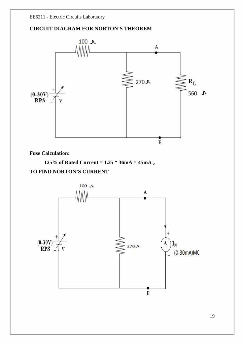
CIRCUIT DIAGRAM FOR NORTON’S THEOREM
Fuse Calculation:
125% of Rated Current = 1.25 * 36mA = 45mA
TO FIND NORTON’S CURRENT

EE6211 - Electric Circuits Laboratory
20
NORTON’S THEOREM
Statement:
Any two-terminal linear network, composed of voltage sources, current
sources, and resistors, can be replaced by an equivalent two-terminal network
consisting of an independent current source in parallel with a resistor. The value of the
current source is the short circuit current (IN) between the two terminals of the
network and the resistance is equal to the equivalent resistance (RN) measured
between the terminals with all energy sources replaced by their internal resistances.
Circuit
RNIN

EE6211 - Electric Circuits Laboratory
21
TO FIND NORTON’S RESISTANCE
NORTON’S EQUIVALENT CIRCUIT
OBSERVATION TABLE
S.
NoVdc
Rth
(Ω)
IN
(mA)
Current through
Load Resistance
IL(mA)
Practical
Value
Theoretical
Value
Practical
Value
Theoretical
Value
Practical
Value
Theoretical
Value
1.
2.
3.
4.
5
2
4
6
8
10

EE6211 - Electric Circuits Laboratory
22
PROCEDURE:
1. Give connections as per the circuit diagram.
2. Measure the current through RL in ammeter.
3. Short circuit A and B through an ammeter.
4. Measure the Norton current in the ammeter.
5. Find out the Norton’s Resistance viewed from the output terminals.
6. Give connections as per the Norton’s Equivalent circuit.
7. Measure the current through RL.
8. Verify Norton’s theorem by comparing currents in RL directly and that
obtained with the equivalent circuit.

EE6211 - Electric Circuits Laboratory
23
CIRCUIT DIAGRAM FOR SUPERPOSITION THEOREM
CIRCUIT DIAGRAM WITH V1 ACTING INDEPENDENTLY
Fuse Calculation:
125% of Rated Current = 1.25 * 21mA = 26.25mA

EE6211 - Electric Circuits Laboratory
24
SUPERPOSITION THEOREM
Statement:
In any linear, bilateral network energized by two or more sources, the total
response is equal to the algebraic sum of the responses caused by individual sources
acting alone while the other sources are replaced by their internal resistances.
To replace the other sources by their internal resistances, the voltage sources
are short- circuited and the current sources open-circuited.

EE6211 - Electric Circuits Laboratory
25
CIRCUIT DIAGRAM WITH V2 ACTING INDEPENDENTLY
OBSERVATION TABLE
Experimental Values Theoretical Values
V1
(Volts)
V2
(Volts)
I3
(mA)
2
4
6
8
10
V1
(Volts)
V2
(Volts)
I3
(mA)
2
4
6
8
10

EE6211 - Electric Circuits Laboratory
26
FORMULAE:
I3’ + I3
’’ = I3
PROCEDURE:
1. Connections are made as per the circuit diagram given in Fig. 1.
2. Switch on the supply.
3. Note the readings of three Ammeters.
4. One of the voltage source V1 is connected and the other voltage source
V2 is short circuited as given in Fig.2.
5. Note the three ammeter readings.
6. Now short circuit the voltage source V1 and connect the voltage source
V2 as given in the circuit diagram of Fig. 3.
7. Note the three ammeter readings.
8. Algebraically add the currents in steps (5) and (7) above to compare
with the current in step (3) to verify the theorem.
9. Verify with theoretical values.

EE6211 - Electric Circuits Laboratory
27
VERIFICATION OF SUPERPOSITION THEOREM
Practical:
S.No.I3
(mA)
I3’
(mA)
I3’’
(mA)
I3= I3’ +I3’’
(mA)
Theoretical:
S.No.I3
(mA)
I3’
(mA)
I3’’
(mA)
I3= I3’ +I3’’
(mA)

EE6211 - Electric Circuits Laboratory
28
MODEL CALCULATION

EE6211 - Electric Circuits Laboratory
29
CIRCUIT DIAGRAM FOR MAXIMUM POWER TRANSFER THEOREM
OBSERVATION TABLE
S.No. RL (Ω)
IL (mA) P = I2RL (mW)
Practical
Value
Theoretical
Value
Practical
Value
Theoretical
Value

EE6211 - Electric Circuits Laboratory
30
MAXIMUM POWER TRANSFER THEOREM
Statement:
The Maximum Power Transfer Theorem states that maximum power is
delivered from a source to a load when the load resistance is equal to source
resistance.
PROCEDURE:
1. Find the Load current for the minimum position of the Rheostat theoretically.
2. Select the ammeter Range.
3. Give connections as per the circuit diagram.
4. Measure the load current by gradually increasing RL .
5. Enter the readings in the tabular column.
6. Calculate the power delivered in RL.
7. Plot the curve between RL and power.
8. Check whether the power is maximum at a value of load resistance that equals
source resistance.
9. Verify the maximum power transfer theorem.

EE6211 - Electric Circuits Laboratory
31
MODEL GRAPH
MODEL CALCULATION

EE6211 - Electric Circuits Laboratory
32
VIVA QUESTIONS:
1. What is meant by a linear network?
2. State Thevenin’s Theorem.
3. How do you calculate thevenin’s resistance?
4. State Norton’s Theorem.
5. Give the usefulness of thevenin’s and Norton’s theorems.
6. State Superposition Theorem.
7. What is meant by a linear system?
8. Give the usefulness of Superposition Theorem.
9. How will you apply Superposition Theorem to a linear circuit containing
both dependent and independent sources?
10. State the limitations of Superposition theorem.
11. Define Power. What is the unit of Power?
12. State Maximum Power Transfer Theorem.
INFERENCE:
RESULT:
Thus the network theorems (Thevenin, Norton, Superposition and Maximum
power transfer theorem) are verified.

EE6211 - Electric Circuits Laboratory
33
BLOCK DIAGRAM OF GENERAL PURPOSE CRO
OBSERVATION TABLE
S.No Type ofwave
Timeperiod
(T)Amplitude Theoretical
FrequencyPractical
Frequency
1.
2.
3.

EE6211 - Electric Circuits Laboratory
34
EXP. NO.:
DATE:
STUDY OF CRO AND MEASUREMENT OF SINUSOIDAL VOLTAGE,FREQUENCY AND POWER FACTOR
AIM:The aim of the experiment is to understand the operation of cathode rayoscilloscope (CRO) and to become familiar with its usage, also to perform anexperiment using function generator to measure amplitude, time period,frequency & power factor of the time varying signals using a calibrated cathoderay oscilloscope.
APPARATUS REQUIRED:
THEORY:The cathode ray oscilloscope (CRO) provides a visual presentation of anywaveform applied to the input terminal. The oscilloscope consists of thefollowing major subsystems.
Cathode ray tube (CRT) Vertical amplifier Horizontal amplifier Sweep Generator Trigger circuit Associated power supply
It can be employed to measure quantities such as peak voltage, frequency,phase difference, pulse width, delay time, rise time, and fall time.
CATHODE RAY TUBE:The CRT is the heart of the CRO providing visual display of an input signal
waveform. A CRT contains four basic parts: An electron gun to provide a stream of electrons. Focusing and accelerating elements to produce a well define beam of
electrons. Horizontal and vertical deflecting plates to control the path of the
electron beam. An evacuated glass envelope with a phosphorescent which glows visibly
when struck by electron beam.
S.No Name of theComponents/Equipment
Qty
1. CRO 12. Function generator 13. Probes 2

EE6211 - Electric Circuits Laboratory
35
A Cathode containing an oxide coating is heated indirectly by a filament resultingin the release of electrons from the cathode surface. The control grid which has anegative potential, controls the electron flow from the cathode and thus control thenumber of electron directed to the screen. Once the electron passes the control grid,they are focused into a tight beam and accelerated to a higher velocity by focusing andaccelerating anodes. The high velocity and well defined electron beam then passedthrough two sets of deflection plates.
The First set of plates is oriented to deflect the electron beam vertically. The angleof the vertical deflection is determined by the voltage polarity applied to the deflectionplates. The electron beam is also being deflected horizontally by a voltage applied tothe horizontal deflection plates. The tube sensitivity to deflecting voltages can beexpressed in two ways that are deflection factor and deflection sensitivity.
The deflected beam is then further accelerated by very high voltages applied to thetube with the beam finally striking a phosphorescent material on the inside face of thetube. The phosphor glows when struck by the energetic electrons.
CONTROL GRID:Regulates the number of electrons that reach the anode and hence the
brightness of the spot on the screen.
FOCUSING ANODE:Ensures that electrons leaving the cathode in slightly different directions are
focused down to a narrow beam and all arrive at the same spot on the screen.
ELECTRON GUN:Cathode, control grid, focusing anode and accelerating anode.
DEFLECTING PLATES:Electric fields between the first pair of plates deflect the electrons horizontally
and an electric field between the second pair deflects them vertically. If no deflectingfields are present, the electrons travel in a straight line from the hole in theaccelerating anode to the center of the screen , where they produce a bright spot. Ingeneral purpose oscilloscope, amplifier circuits are needed to increase the input signalto the voltage level required to operate the tube because the signals measured usingCRO are typically small. There are amplifier sections for both vertical and horizontaldeflection of the beam.
VERTICAL AMPLIFIER:Amplify the signal at its input prior to the signal being applied to the vertical
deflection plates.

EE6211 - Electric Circuits Laboratory
36
HORIZONTAL AMPLIFIER:Amplify the signal at its input prior to the signal being applied to the horizontal
deflection plates.
SWEEP GENERATOR:Develop a voltage at the horizontal deflection plate that increases linearly with
time.
OPERATION:The four main parts of the oscilloscope CRT are designed to create and direct
an electron beam to a screen to form an image. The oscilloscope links to a circuit thatdirectly connects to the vertical deflection plates while the horizontal plates havelinearly increasing charge to form a plot of the circuit voltage over time. In anoperating cycle, the heater gives electrons in the cathode enough energy to escape.The electrons are attracted to the accelerating anode and pulled through a control gridthat regulates the number of electrons in the beam, a focusing anode that controls thewidth of the beam, and the accelerating anode itself. The vertical and horizontaldeflection plates create electric field that bend the beam of electrons. The electronsfinally hit the fluorescent screen which absorbs the energy from the electron beam nademits it in the form of light to display an image at the end of the glass tube.
PRECAUTIONS:
1. Do not leave a ‘bright spot’ on the screen for any length of time.
2. Do not apply signals that exceed the scopes voltage rating.
3. Do not try make accurate measurements on signals whose frequency is outside
the scope’s frequency specifications.
4. Be aware that the scope’s input circuitry can cause loading effects on the
circuitry under test-use correct probe for the work.

EE6211 - Electric Circuits Laboratory
37
PROCEDURE:
1. Measurement of Voltage Using CRO: A voltage can be measured by notingthe Y deflection produced by the voltage; using this deflection in conjunction with theY-gain setting, the voltage can be calculated as follows : V = ( no. of boxes in cm. ) x( selected Volts/cm scale )
2 .Measurement of Current and Resistance Using a CRO: Using the generalmethod, a correctly calibrated CRO can be used in conjunction with a known value ofresistance R to determine the current I flowing through the resistor.
3 Measurement of Frequency Using a CRO: A simple method of determiningthe frequency of a signal is to estimate its periodic time from the trace on the screen ofa CRT. However this method has limited accuracy, and should only be used whereother methods are not available. To calculate the frequency of the observed signal, onehas to measure the period, i.e. the time taken for 1 complete cycle, using the calibratedsweep scale. The period could be calculated by T = (no. of squares in cm) x (selectedTime/cm scale) Once the period T is known, the frequency is given by f (Hz) = 1/T(sec).
4. Measurement of Phase: The calibrated time scales can be used to calculatethe phase shift between two sinusoidal signals of the same frequency. If a dual trace orbeam CRO is available to display the two signals simultaneously (one of the signals isused for synchronization), both of the signals will appear in proper time perspectiveand the amount of time difference between the waveforms can be measured. This, inturn can be utilized to calculate the phase angle θ, between the two signals.Referring to the fig. the phase shift can be calculated by the formula;
θ°=
MEASUREMENT OF POWER FACTOR:
The power factor is calculated by the formulaPf= VICOSϕ
.

EE6211 - Electric Circuits Laboratory
38
VIVA QUESTIONS:1. What is a CRO?2. How can we measure the voltage using a CRO?3. Explain the different parts of the CRO4. Explain the operation of a CRO.
INFERENCE:
RESULT:Thus, the performance and operation of CRO is studied.

EE6211 - Electric Circuits Laboratory
39
CIRCUIT DIAGRAM FOR SERIES RESONANCE
MODEL GRAPH FOR SERIES RESONANCE
Imax
0.707Imax
Current in mA
f1 fr f2
A B
Frequency in Hz

EE6211 - Electric Circuits Laboratory
40
EXP. NO.:
DATE:
DESIGN AND SIMULATION OF SERIES RESONANCE CIRCUIT
AIM:To plot the magnitude & phase angle of current for various frequencies for the
given RLC series circuit.
SOFTWARE REQUIRED:Matlab 7.1
THEORY:
A circuit is said to be in resonance when applied voltage V and current I are in
phase with each other. Thus at resonance condition, the equivalent complex
impedance of the circuit consists of only resistance (R) and hence current is
maximum. Since V and I are in phase, the power factor is unity.
The complex impedance
Z = R + j (XL – XC)
WhereXL = L
XC = 1/C
At resonance, XL= XC and hence Z= R
BANDWIDTH OF A RESONANCE CIRCUIT:
Bandwidth of a circuit is given by the band of frequencies which lies between
two points on either side of resonance frequency, where current falls through 1/1.414
of the maximum value of resonance. Narrow is the bandwidth, higher the selectivity
of the circuit. As shown in the model graph, the bandwidth AB is given by f2 – f1. f1 is
the lower cut off frequency and f2 is the upper cut off frequency.

EE6211 - Electric Circuits Laboratory
41
PLOT OF MAGNITUDE & PHASE ANGLE OF CURRENT FOR VARIOUSFREQUENCIES

EE6211 - Electric Circuits Laboratory
42
PROCEDURE:
1. Open a new MATLAB/SIMULINK model
2. Connect the circuit as shown in the figure
3. Debug and run the circuit
4. By double clicking the powergui plot the value of current for the
different values of frequencies.
VIVA QUESTIONS:
1. What is meant by resonance?
2. What are the characteristics of a series resonant circuit?
3. What will be the power factor of the circuit at resonance?
INFERENCE:
RESULT:
Thus, the plot of the magnitude & phase angle of current for variousfrequencies for the given RLC series circuit is done.

EE6211 - Electric Circuits Laboratory
43
CIRCUIT DIAGRAM FOR PARALLEL RESONANCE
MODEL GRAPH FOR PARALLEL RESONANCE
Frequency in Hz
Imin
fr
Cur
rent
in m
A

EE6211 - Electric Circuits Laboratory
44
EXP. NO.:
DATE:
DESIGN AND SIMULATION OF PARALLEL RESONANCE CIRCUIT
AIM:To plot the magnitude & phase angle of current for various frequencies for the
given RLC parallel circuit.
SOFTWARE REQUIRED:Matlab 7.1
THEORY:
A circuit is said to be in resonance when applied voltage V and current I are in
phase with each other. Thus at resonance condition, the equivalent complex
impedance of the circuit consists of only resistance (R) and hence current is
maximum. Since V and I are in phase, the power factor is unity.
The complex impedance
Z = R + j (XL – XC)
WhereXL = L
XC = 1/C
At resonance, XL= XC and hence Z= R
BANDWIDTH OF A RESONANCE CIRCUIT:
Bandwidth of a circuit is given by the band of frequencies which lies between
two points on either side of resonance frequency, where current falls through 1/1.414
of the maximum value of resonance. Narrow is the bandwidth, higher the selectivity
of the circuit. As shown in the model graph, the bandwidth AB is given by f2 – f1. f1 is
the lower cut off frequency and f2 is the upper cut off frequency.

EE6211 - Electric Circuits Laboratory
45
PLOT OF MAGNITUDE & PHASE ANGLE OF CURRENT FOR VARIOUSFREQUENCIES

EE6211 - Electric Circuits Laboratory
46
PROCEDURE:
1. Open a new MATLAB/SIMULINK model
2. Connect the circuit as shown in the figure
3. Debug and run the circuit
4. By double clicking the powergui plot the value of current for the
different values of frequencies.
VIVA QUESTIONS
1. What are the characteristics of a parallel resonant circuit?
2. What is meant by resonant frequency?
3. Define Bandwidth.
4. Define Quality factor.
5. How is upper and lower cut- off frequencies determined?
6. What is meant by selectivity?
7. Give the significance of Q- factor.
INFERENCE:
RESULT:Thus the plot of the magnitude & phase angle of current for various frequencies
for the given RLC parallel circuit is done.

EE6211 - Electric Circuits Laboratory
47
CIRCUIT DIAGRAM: Low pass Filter
Scope result for Amplitude=5; Frequency=1:
Scope result for Amplitude=5; Frequency=10

EE6211 - Electric Circuits Laboratory
48
EXP. NO.:
DATE:SIMULATION OF LOW PASS AND HIGH PASS PASSIVE FILTERS
AIM:To design the low pass and high pass passive filters for specified cut off
frequencies.
SOFTWARE REQUIRED:Matlab 7.1
THEORY:
Filter is a frequency selective network , which passes desired range of
frequencies from the input to the output by rejecting(filtering) other frequency signals.
The filter can be broadly classified into active filters and passive filters. According to
their characteristics they can be classified into,
1. Low pass filter which allows only low frequency signals
2. High pass filter which allows only high frequency signals
3. Pass band filter which allows only certain range of frequency signals.
4. Stop band filter which rejects the particular range of frequency signals.
LOW PASS FILTER:
The magnitude response of an ideal low pass filter allows low frequencies in
the passband i.e., 0<ω<ωc to pass, whereas the higher frequencies ω>ωc are blocked.
The frequency ωc is the cut off frequency between two pass bands, where the
magnitude is 0.707.
Cut off frequency ωc = 1/RC
H(s) =Vo (s)/Vin(s) =(1/RC)/(s+RC)
Where, s- complex value; for sinusoidal signal s=jɷ
H(jɷ)= (1/RC)/( jɷ +RC)
| H(jɷ)|= (1/RC)/√( ɷ2 +(1/RC)2
angle H(jɷ)= -tan-1(ɷ/RC)

EE6211 - Electric Circuits Laboratory
49
MODEL GRAPH FOR LPF
PLOT OF MAGNITUDE & PHASE ANGLE

EE6211 - Electric Circuits Laboratory
50
PROCEDURE FOR LPF:
1. Open a new MATLAB/SIMULINK model.
2. Connect the circuit as shown in the figure.
3. Debug and run the circuit.
4. By using scope we can observe graph for various frequencies.
5. To obtain bode plot for LPF, type the following codes in command
window.
num= 10
den=[1 10]
sys=tf(num,den)
bode(sys)

EE6211 - Electric Circuits Laboratory
51
CIRCUIT DIAGRAM: High pass Filter
Scope result for Amplitude=1; Frequency=1:
Scope result for Amplitude=1; Frequency=100000:

EE6211 - Electric Circuits Laboratory
52
HIGH PASS FILTER:
The magnitude response of an ideal high pass filter allows high frequencies i.e.,
ω>ωc to pass, and rejects the frequencies ω=0 and ω=ωc. The frequency ωc is the cut
off frequency at the magnitude is 0.707
Cut off frequency ωc = 1/RC
Vo = [R/(C+R)]Vin
Vo = R/[(1/jɷc)+R] Vin
Vo = jɷcR/(1+ jɷcR) Vin
Vo =[ jɷ/(1/CR)]/[1+ jɷ/ (1/CR)] Vin
Let ɷc= 1/CR=2∏fc
Vo =(jɷ/2∏fc)/[1+(jɷ/2∏fc)] Vin
PROCEDURE FOR HPF:
1. Open a new MATLAB/SIMULINK model.
2. Connect the circuit as shown in the figure.
3. Debug and run the circuit.
4. By using scope we can observe graph for various frequencies.
5. To obtain bode plot for LPF, type the following codes in command
window.
num= [1/(2*3.14*100) 0]
den=[1/(2*3.14*100) 1]
sys=tf(num,den)bode(sys)

EE6211 - Electric Circuits Laboratory
53
MODEL GRAPH
PLOT OF MAGNITUDE & PHASE ANGLE

EE6211 - Electric Circuits Laboratory
54
VIVA QUESTIONS:1. What is meant by passive filter?2. List the different types of filter.3. What is cutoff frequency?
INFERENCE:
RESULT:Thus, the simulation of low pass filter and high pass filter is done and their
outputs are noted.

EE6211 - Electric Circuits Laboratory
55
CIRCUIT DIAGRAM:
SIMULATION OF BALANCED/UNBALANCED STAR CONNECTED CIRCUIT
MODEL GRAPH

EE6211 - Electric Circuits Laboratory
56
EXP. NO.:
DATE:
SIMULATION OF THREE PHASE BALANCED AND UNBALANCED STAR,DELTA NETWORKS CIRCUITS
AIM:To design three phase balanced and unbalanced star, delta networks circuits.
SOFTWARE REQUIRED:Matlab 7.1
THEORY:
Balanced three- phase circuit:
Balanced phase voltages are equal in magnitude and are out of phase
with each other by 120°.The phase sequence is the time order in which the voltages
pass through their respective maximum values. A balanced load is one in which the
phase impedances are equal in magnitude and in phase.
Possible Load Configurations
Four possible connections between source and load:
1. Y-Yconnection (Y-connected source with a Y-connected load)
2. Y-∆connection (Y-connected source with a ∆-connected load)
3. ∆-∆connection
4. ∆-Yconnection
Unbalanced three- phase circuit:
An unbalanced system is due to unbalanced voltage sources or an unbalanced
load. To calculate power in an unbalanced three-phase system requires that we find
the power in each phase. The total power is not simply three times the power in one
phase but the sum of the powers in the three phases.

EE6211 - Electric Circuits Laboratory
57
CIRCUIT DIAGRAM:
SIMULATION OF BALANCED/UNBALANCED DELTA CONNECTED CIRCUIT
MODEL GRAPH:

EE6211 - Electric Circuits Laboratory
58
VIVA QUESTIONS:
1. What do you meant by balanced circuit?
2. List the possible load configuration?
3. What is mean by unbalanced circuit?
INFERENCE:
RESULT:Thus the simulation of balanced/unbalanced star & delta connected circuits has been
done and the output graph is observed.

EE6211 - Electric Circuits Laboratory
59
CIRCUIT DIAGRAM:
Fuse Calculation:125% of rated current = 1.25 * 5.2 = 6.5A
Name Plate Details
Switch
I=6A, V=240V
Autotransformer
3 Phase V=415V
Voltmeter
V=(0-600)V,MI
Ammeter
I=(0-10A),MI
Watt meter
V=250V, I= 5A, UPF
Variable Resistive Load
3 Phase Load, 415V, 5 H.P

EE6211 - Electric Circuits Laboratory
60
EXP. NO.:
DATE:
EXPERIMENTAL DETERMINATION OF POWER IN THREE PHASECIRCUITS BY TWO-WATT METER METHOD
AIM:To determine the power in three-phase balanced and unbalanced circuit using
two-watt meter method.
APPARATUS REQUIRED:
THEORY:Two wattmeter method can be employed to measure power in a 3- phase,3 wire
star or delta connected balance or unbalanced load. In this method, the current coils ofthe watt meters are connected in any two lines say R and Y and potential coil of eachwatt meters is joined across the same line and third line i.e. B. Then the sum of thepower measured by two watt meters W1 and W2 is equal to the power absorbed Bythe 3- phase load
PROCEDURE:1. Connect the Voltmeter, Ammeter and Watt meters to the load through 3ф
Autotransformer as shown fig and set up the Autotransformer to Zero position.2. Switch on the 3ф A.C. supply and adjust the autotransformer till a suitable
voltage.3.Note down the readings of watt meters, voltmeter& ammeter4. Vary the voltage by Autotransformer and note down the Various readings.5. Now after the observation switch off and disconnect all the Equipment or
remove the lead wire.
FORMULAE USED:1. Total power or Real power P = √3VLILCOSф =W1actual+W2actual
2. Reactive power of load= Q=√3(W1actual-W2actual)3. tan ф= [√3(W1actual-W2actual)]/[ W1actual+W2actual]
4. Power factor=cos ф
SLNO NAME OF ITEM SPECIFICATION QUANTITY1. 3-phase Auto transformer 20 A, 440v 50 Hz 12. Ammeter MI(0-10A) 13. Voltmeter MI(0-600V) 14. Wattmeter 250v, 5A 2
5.3- phase Load or 3- phaseinduction motor
415V, 5H.P 1
6 Connecting wires - Few

EE6211 - Electric Circuits Laboratory
61
OBSERVATION TABLE
MODEL CALCULATION
Sl.No.
Voltmeterreading
VL
Ammeter reading
IL
Wattmeter reading(watts)
Totalpower
P
Reactivepower
Q Powerfactor
(V) (A) W1
ObservedW1
ActualW2
ObsW2
Act (watts) (watts)

EE6211 - Electric Circuits Laboratory
62
PRECAUTION & SOURCES OF ERROR:1. Proper currents and voltage range must be selected before putting the
instruments in the circuit.2. If any Wattmeter reads backward, reverse its pressure coil connection and
the reading as negative.3. As the supply voltage Fluctuates it is not possible to observe the readings
correctly.
VIVA QUESTIONS:1. What are the various types of wattmeter?2. How many coils are there in wattmeter?3. What is meant by real power?4. What is meant by apparent power?
INFERENCE:
RESULT:Thus, the power is measured in the 3-phase circuit and there corresponding
power factors are observed.

EE6211 - Electric Circuits Laboratory
63
CIRCUIT DIAGRAM
Fuse Calculation:
125% of rated current = 1.25 * 21.739A = 27.12A
Name Plate Details
Switch
I=6A, V=240V
Autotransformer
V=230V
Voltmeter
V=(0-300)V,MI
Ammeter
I=(0-10A),MI
Watt meter
V=300V, I= 10A, LPF
Variable Resistive Load
P=5KW
Energy Meter
I=5-20A, V=240V, 1200 Revs/KWh

EE6211 - Electric Circuits Laboratory
64
EXP. NO.:
DATE:CALIBRATION OF SINGLE PHASE ENERGY METER
AIM:To calibrate the energy consumed in a single phase circuit using single phase
energy meter.
APPARATUS REQUIRED:S.NO COMPONENTS RANGE TYPE QUANTITY
1 Ammeter (0-10)A MI 12 Voltmeter (0-300)V MI 13 Load 5kW Resistive 1
4 Energy meter300V, 10A,Single phase
UPF 1
5 Wires - - As required6 Tester - - 17 Wattmeter 300V, 10A UPF 1
THEORY:Energy meters are integrating instruments and are used for measurement of
energy in a circuit over a given time. Since the working principle of such instrumentsis based on electromagnetic induction, these are known as induction type energymeters. The fig. 1 explains the working of such instrument.
Here are two coils in an induction type energy meter, namely current coil (cc)and voltage coil (vc). The current coil is connected in series with the load while thevoltage coil is connected across the load. The aluminum disc experiences deflectingtorque due to eddy currents induced in it and its rotations are counted by a gear trainmechanism (not shown in fig.)
The ratings associated with the energy meter areVoltage ratingCurrent ratingFrequency ratingMeter constant.
FORMULAE USED:1. Actual wattmeter reading= Observed wattmeter reading * Multiplication
factor (MF)
2. Using energy meter constant 1200 revolution = 1kWh
1 revolution = 1*1000*3600/1200 =3000 Watts sec.ie Ke = 3000 Watts sec.
3. Measured wattmeter reading = [(Ke * n)/ t] Watts.
Where. t – Time taken for n revolutions in seconds.4. % Error = [(Wact – W meas)/ Wact]* 100

EE6211 - Electric Circuits Laboratory
65
OBSERVTION TABLEMultiplication factor (MF) = (VIcosф )/ full scale deflection=_______Number of revolution n= ____
S.NO
Ammeterreading
(A)
Voltmeterreading
(V)
WattmeterReading
TimeTaken
For‘n’
Revolution
Measuredwattmeter
readingW measured
%ErrorObserved
Wobser
ActualWactual
MODEL GRAPH
MODEL CALCULATION

EE6211 - Electric Circuits Laboratory
66
PROCEDURE:1. Connections are given as shown in circuit diagram.
2. Supply is switched on and load is increased in steps, each time note downthe readings of ammeter, voltmeter and wattmeter. Also the time taken for nrevolution of the disc is measured using stop watch.
3. Step 2 is repeated till rated current of the energy meter is reached.
4. % Error is calculated and calibration curve is drawn.
VIVA QUESTIONS:
1. What is enery meter constant?
2. What is the unit of energy?
3. What are the ratings associated with energy meter?
INFERENCE:
RESULT:Thus the calibration of energy meter is done and the error values are calculated
for different loads.

EE6211 - Electric Circuits Laboratory
67
CIRCUIT DIAGRAM FOR TWO-PORT NETWORK
OBSERVATION TABLE
S.No V1
(Volts)V2
(Volts)I1
(Amps)I2
(Amps)Z11
(Ohms)Z12
(Ohms)Z22
(Ohms)Z21
(Ohms)

EE6211 - Electric Circuits Laboratory
68
EXP. NO.:
DATE:DETERMINATION OF TWO PORT NETWORK PARAMETERS
AIM:To determine the two port parameters for the given electric circuit.
APPARATUS REQUIRED:
THEORY:
1 2
1’ 2’
The terminal pair where the signal enters the network is called as the INPUT
PORT and the terminal pair where it leaves the network is called as the OUTPUT
PORT. V1& I1 are measured at the Input terminals and V2 & I2 are measured at the
Output terminals. The two port network parameters express the inter relationship
between V1, I1,V2 and I2 They are Z- parameters, Y- parameters, H-parameters, ABCD
parameters and image parameters.
The Impedance parameters are also called as Z parameters.V1 = Z11I1 + Z12I2 …………..……. (i)V2 = Z21I1 + Z22I2 …………..……. (ii)
S.NO Name of theApparatus/Component Range Type Quantity
1Ammeter
(0-25)mA MC 2
2DC Power Supply
(0-30)V RPS 2
3 Resistor 100Ω Fixed 3
4 Connecting wires - Single Strand As Required
5 Breadboard - - 1
Linear Network

EE6211 - Electric Circuits Laboratory
69
MODEL CALCULATION

EE6211 - Electric Circuits Laboratory
70
where, Z11, Z12, Z22 and Z21 are constants of the network called Z parameters.
When I2=0, (Open circuit the output terminal)
Z11=V1/I1 ….……………... (iii)Z21=V2/I1 ..……………....... (iv)
When I1=0, ( Open circuit the Input terminal)
Z12=V1/I2 ….……………... (v)Z22=V2/I2 ….……………... (vi)
PROCEDURE:
1. Connect the circuit as per the circuit diagram.
2. Open circuit the output terminal (2,2’).
3. Vary the power supply to a fixed value and note down the ammeter and
voltmeter readings.
4. Open circuit the Input terminal (1,1’).
5. Vary the power supply to a fixed value and note down the ammeter and
voltmeter readings.
6. Tabulate the readings and calculate the Z parameters.
VIVA QUESTIONS:1. What is meant by a two-port network?
2. Give the use of two-port network model.
3. What are impedance parameters?
4. What are admittance parameters?
5. What are hybrid parameters?
6. What are ABCD parameters? Mention their significance.
INFERENCE:
RESULT:Thus the two port parameters are measured for the given electric circuit.

EE6211 - Electric Circuits Laboratory
71
CIRCUIT DIAGRAM FOR RC TRANSIENT:
Name Plate Details
Function Generator: 20 V, 500ΩDecade Capacitance Box: 1µfd – 1000pfd
MODEL GRAPH

EE6211 - Electric Circuits Laboratory
72
RC
tin
C eR
VI
)1( RC
t
inC eVV
)1( 1 eVV inC
EXP. NO.:
DATE:
EXPERIMENTAL DETERMINATION OF TIME CONSTANT OF SERIESR-C ELECTRIC CIRCUIT
AIM:
To find the time constant of series R-C electric circuits
APPARATUS REQUIRED:
S.No.Name of the
Components/EquipmentRange/Type
Quantityrequired
1 Resistor 100 Ώ 12 Function generator 20 V, 500Ω 13 Voltmeter (0-30)V MI 1
4 Decade capacitance box1µfd –
1000pfd1
5 Wires Single strand As Required6 Bread board - 1
THEORY:RC Circuit:
Consider a series RC circuit as shown. The switch is in open state initially.
There is no charge on condenser and no voltage across it. At instant t=0, switch is
closed.
Immediately after closing a switch, the capacitor acts as a short circuit, so
current at the time of switching is high. The voltage across capacitor is zero at t= 0+ as
capacitor acts as a short circuit, and the current is maximum given by,
i = V/R Amps
This current is maximum at t=0+ which is charging current. As the capacitor
starts charging, the voltage across capacitor VC starts increasing and charging current
starts decreasing. After some time, when the capacitor charges to V volts, it achieves
steady state. In steady state it acts as an open circuit and current will be zero finally.
Charging current and voltage in capacitor are given as below

EE6211 - Electric Circuits Laboratory
73
OBSERVATION TABLE
S.No. Frequency(Hz)
Time(s)
Voltage across thecapacitor VC
(v)
MODEL CALCULATION

EE6211 - Electric Circuits Laboratory
74
The term RC in equation of VC or IC is called Time constant and denoted by ,
measured in seconds.
when t = RC = then,
VC = 0.632Vin
So time constant of series RC circuit is defined as time required by the
capacitor voltage to rise from zero to 0.632 of its final steady state value during
charging.
Thus, time constant of RC circuit can be defined as time seconds, during which
voltage across capacitor (stating from zero) would reach its final steady state value if
its rate of change was maintained constant at its initial value throughout charging
period.
PROCEDURE:
1. Make the connections as per the circuit diagram
2. Vary the frequency by using function generator
3. For different frequencies tabulate the value of voltage across the capacitor
4. Calculate the time period
5. Plot the graph for time period Vs voltage across the capacitor.
VIVA QUESTIONS:
1. Differentiate steady state and transient state.
2. What is meant by transient response?
3. Define the time constant of a RL Circuit.
4. Define the time constant of a RC Circuit.
5. What is meant by forced response?
INFERENCE:
RESULT:
Thus the transient responses of RC circuit is found practically.

EE6211 - Electric Circuits Laboratory
75
CIRCUIT DIAGRAM FOR SERIES RESONANCE
CIRCUIT DIAGRAM FOR PARALLEL RESONANCE
Name Plate Details
Function Generator: 20 V, 500ΩDecade Capacitance Box: 1µfd – 1000pfdDecade Inductance Box: 1µH – 1000µH
EE6211 - Electric Circuits Laboratory
76
EXP. NO.:
DATE:
FREQUENCY RESPONSE OF SERIES AND PARALLEL RESONANCECIRCUITS
AIM:To plot the current Vs frequency graph of series and parallel resonant circuits
and hence measure their bandwidth, resonant frequency and Q factor.
APPARATUS REQUIRED:
S.No. Name of theComponents/Equipment
Type Range Quantityrequired
1 Function Generator - 20 V, 500Ω 12 Resistor Fixed 100 Ω 13 Decade Inductance Box Variable 1µH – 1000µH 14 Decade Capacitance Box Variable 1µfd – 1000pfd 15 Ammeter MI (0-30) mA 16 Connecting Wires Single
Strand- As
Required
THEORY:
A circuit is said to be in resonance when applied voltage V and current I are in
phase with each other. Thus at resonance condition, the equivalent complex
impedance of the circuit consists of only resistance (R) and hence current is
maximum. Since V and I are in phase, the power factor is unity.
The complex impedance
Z = R + j (XL – XC)
WhereXL = L
XC = 1/C
At resonance, XL= XC and hence Z= R

EE6211 - Electric Circuits Laboratory
77
OBSERVATION TABLE
Series Resonance
Sl. No. L XL C XC
Frequency
(HZ)
Output
Current
(mA)
Parallel Resonance
Sl. No. L XL C XC
Frequency
(HZ)
Output
Current
(mA)

EE6211 - Electric Circuits Laboratory
78
BANDWIDTH OF A RESONANCE CIRCUIT:
Bandwidth of a circuit is given by the band of frequencies which lies between
two points on either side of resonance frequency, where current falls through 1/1.414
of the maximum value of resonance. Narrow is the bandwidth, higher the selectivity
of the circuit.
As shown in the model graph, the bandwidth AB is given by f2 – f1. f1 is the
lower cut off frequency and f2 is the upper cut off frequency.
Q - Factor:In the case of a RLC series circuit, Q-factor is defined as the voltage
magnification in the circuit at resonance. At resonance, current is maximum. Io= V/R.
The applied voltage V = IoR
Voltage magnification = VL/V = IoXL
In the case of resonance, high Q factor means not only high voltage, but also
higher sensitivity of tuning circuit. Q factor can be increased by having a coil of
large inductance, not of smaller ohmic resistance.
Q = L / R
FORMULAE USED:
Resonant frequency fr =LC2
1Hz
Bandwidth BW = f2 – f1
Quality Factor =BW
f r
PROCEDURE:
1. Connect the circuit as per the circuit diagram.
2. Vary the frequency and note down the corresponding meter reading.
3. Draw the current Vs frequency curve and measure the bandwidth, resonant
frequency and Q factor.

EE6211 - Electric Circuits Laboratory
79
MODEL GRAPH FOR SERIES RESONANCE
Imax
0.707Imax
MODEL GRAPH FOR PARALLEL RESONANCE
Frequency in Hz
Current in mA
f1 fr f2
A B
Frequency in Hz
Imin
fr
Cur
rent
in m
A

EE6211 - Electric Circuits Laboratory
80
VIVA QUESTIONS:
1. Define Bandwidth.
2. Define Quality factor.
3. What is meant by selectivity?
4. Give the significance of Q- factor.
INFERENCE:
RESULT:
Thus the current Vs frequency graphs of series and parallel resonant circuits
were plotted and the bandwidth, resonant frequency and Q factor were measured.
They were found to be
(a) Series resonance
Resonant frequency = ____________
Bandwidth = ____________
Q- Factor = ____________
(b) Parallel Resonance
Resonant frequency = ____________
Bandwidth = ____________
Q- Factor = ____________

EE6211 - Electric Circuits Laboratory
81
CIRCUIT DIAGRAM
Figure 1Fuse Calculation:
125% of rated current = 1.25*14.1mA = 17.63 mA.
Figure 2

EE6211 - Electric Circuits Laboratory
82
EXP. NO.:
DATE:
VERIFICATION OF RECIPROCITY THEOREM
AIM:
To verify Reciprocity theorem for a given network.
APPARATUS REQUIRED:
S.NO. Name of the Apparatus Range Quantity1 Bread Board - 12 Resistor 1 KΩ 33 Resistor 2.2 KΩ 34 Ammeterer 0-10 mA 15 Voltmeter 0-30 V 16 RPS 0-30 V 1
THEORY:
In any linear bilateral network, if a single voltage source Va in branch ‘a’produces a current Ib in branch ‘b’, then if the voltage source Va is removed andinserted in branch ‘b’ will produce a current Ib in branch ‘a’. The ratio ofresponse to excitation is same for the two conditions mentioned above. This is
called the reciprocity theorem. Consider the network shown in figure. AA1 denotes
input terminals and BB1 denotes output terminals. The application of voltage V
across AA1 produces current I at BB1. Now if the position of source and
responses are interchanged, by connecting the voltage source across BB1, the
resultant current I will be at terminals AA1. According to Reciprocitytheorem, the ratio of response to excitation is the same in both cases.

EE6211 - Electric Circuits Laboratory
83
OBSERVATION TABLE
Table 1(for I3):
V1 (v)I3 (mA) R = (V1/ I3) (Ω)
Theoretical Practical Theoretical Practical
Table 2 (for I31):
V1 (v) I31 (mA) R1 = (V1/ I3
1) (Ω)
Theoretical Practical Theoretical Practical

EE6211 - Electric Circuits Laboratory
84
PROCEDURE:
1. Connection are made as per the circuit diagram shown in figure 1.2. Vary the supply voltage V1 and take the corresponding reading I3
from the ammeter.3. Find out the ratio R = (V1/ I3).4. Now interchange the position of ammeter and Variable voltage supply
V1 as shown in figure 2.
5. Vary the supply voltage V1 and take the corresponding reading I31
from the ammeter.6. Find out the ratio R1 = (V1/ I31).7. Now check whether R and R1 are same.
INFERENCE:
RESULT:
Thus the reciprocity theorem was verified.

EE6211 - Electric Circuits Laboratory
85
Figure 3
Fuse Calculation:125% of rated current = 1.25 * 0.02 = 25mA
Figure 4
Figure 5

EE6211 - Electric Circuits Laboratory
86
EXP. NO.:
DATE:VERIFICATION OF COMPENSATION THEOREM
AIM:
To verify Compensation theorem for the given network.
APPARATUS REQUIRED:
S.NO. Name of the Apparatus Range Quantity1 Bread Board - 12 Resistor 1 KΩ 33 DRB - 14 Ammeter 0-25 mA 15 Voltmeter 0-30 V 16 RPS 0-30 V 1
THEORY:
The compensation theorem states that any element in the linear, bilateralnetwork, may be replaced by a voltage source of magnitude equal to the currentpassing through the element multiplied by the value of the element, provided thecurrents and voltages in other parts of the circuit remain unchanged. Considerthe circuit shown in figure 1. The element R can be replaced by voltage source V,which is equal to the current I passing through R multiplied by R as shown below.
Figure 1
This theorem is useful in finding the changes in current or voltage when thevalue of resistance is changed in the circuit as shown in figure 2.

EE6211 - Electric Circuits Laboratory
87
OBSERVATION TABLETable 1(for I3):
V1 (v)I3 (mA)
Theoretical Practical
15
Table 2 (for I31):
Radd
(KΩ)I3
1
(mA)
Theoretical Practical
12345
Table 3 (for I3”):
V2 =I3Radd
(v)
I3” (mA)
Theoretical Practical
Table 4 (for Ammeter Reading):
I3 (mA) 11I3 (mA)Ammeter ReadingI = I3 –I 11 (mA)3

EE6211 - Electric Circuits Laboratory
88
Figure 2PROCEDURE:
1. Connection are made as per the circuit diagram shown in figure 3.2. Set the supply voltage V1 = 15 V and take the corresponding reading I3
from the ammeter.3. Now connect the additional resistor (DRB) as shown in figure 4.4. Now fixing V1 =15 V and finding out the current I3 due to extra resistor
DRB where Decade Resistance Box Value is changed correspondingly.5. Now replace the voltage V1 by compensated voltage V2 as shown in fig. 5
and find out the I3 due to compensated voltage V2.6. Finally find the Ammeter Reading I=I3-I3.
INFERENCE:
RESULT:
Thus the Compensation theorem was verified.
Recommended


![A Romantic Jazz Suite [C118] - Free-scores.com : World Free … · eee eee e eee )o 2e %e&o %vq i r x m ± ± m ± ± ± ± ± m ± ± m ± ± ± ± ± " eee eee e eee)o 2e %e&o %vq](https://img.dokumen.tips/doc/110x75/60a6220791891f1ffb1e5d23/a-romantic-jazz-suite-c118-free-world-free-eee-eee-e-eee-o-2e-eo-vq.jpg)