Semiconductor Power Switching Devices-2(Lecture-5)
R S Ananda Murthy
Associate Professor and HeadDepartment of Electrical & Electronics Engineering,
Sri Jayachamarajendra College of Engineering,Mysore 570 006
R S Ananda Murthy Semiconductor Power Switching Devices-2
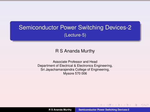
Silicon Controlled Rectifier (SCR)
p+
p
Gate (G)Cathode (K)
Anode (A)
n-
J1
J2n+
J3
Structure of SCR
p+ indicates heavily doped p-type regionn- indicates lightly doped n-type regionn+ indicates heavily doped n-type region
A
KG
Circuit Symbolof SCR
ON
OFF
= Latching Current= Holding Current
ReverseLeakageCurrent
ForwardLeakageCurrent
Thicker n- layer gives higher voltage blocking capability tothe device.The forward voltage at which the device turns ondecreases with increase in gate current.
R S Ananda Murthy Semiconductor Power Switching Devices-2

Control Characteristics of SCR
vo
iG
vo
+
−
iG
V
t
R
−
+
V
t
SCR is semicontrolled and pulse triggered.
R S Ananda Murthy Semiconductor Power Switching Devices-2

Two Transistor Model of SCR
p1
p2
n1
n2
p1
n1
2p
n2
p2
1n
T1
T2
+
−
Gate
Control
Circuit
IG
+
−
IK
IA
α1
IC 1
IC 2
α2 T2
IB 1
IB 2
T1
K
A
K
J1
J2
J3G
R
V
A
K
G
G V
RA
1.0
0.8
0.6
0.4
0.2
00 (mA)1
α
IE
(a) (b)
(c) (d)
R S Ananda Murthy Semiconductor Power Switching Devices-2
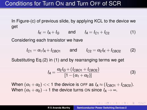
Conditions for Turn ON and Turn OFF of SCR
In Figure-(c) of previous slide, by applying KCL to the device weget
IK = IA + IG and IA = IC1 + IC2 (1)
Considering each transistor we have
IC1 = α1IA + ICBO1 and IC2 = α2IK + ICBO2 (2)
Substituting Eq.(2) in (1) and by rearranging terms we get
IA =α2IG +(ICBO1 + ICBO2)
[1− (α1 +α2)](3)
When (α1 +α2)<< 1 the device is OFF as IA ≈ (ICBO1 + ICBO2).When (α1 +α2)→ 1 the device turns ON since IA→ ∞.
R S Ananda Murthy Semiconductor Power Switching Devices-2

Factors Causing Turn ON of SCR
Forward voltage vAK > VBO. This should be avoided sinceit may permanently damage the device.Rise in device temperature can cause unwanted turn ON
and hence should be avoided by cooling the device.By injecting positive gate current IG until IA = IL where IL isthe latching value. This is the preferred method of turningON the device.Forward dvAK/dt > rated value causes undesirable turnON and should prevented by connecting a snubber circuitacross the SCR.Light radiation of specific wavelength incident on junctionsof SCR turns ON the device. LASCR’s are turned ON bythis method.
R S Ananda Murthy Semiconductor Power Switching Devices-2
How to Turn Off SCR?
Gate current has no control over the SCR after it turns ON.IA should be reduced below the holding value IH in order tomake (α1 +α2)→ 0 to stop the internal regenerative actionto turn OFF the device.After IA drops to zero, the device should be reverse biasedfor a duration tq > tOFF where tOFF is known as the deviceturn OFF time and tq is known as the circuit turn-off time.
R S Ananda Murthy Semiconductor Power Switching Devices-2
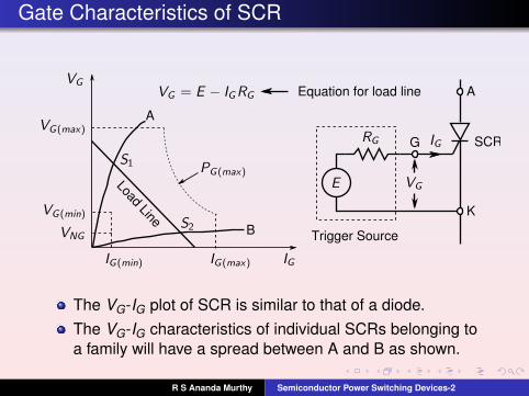
Gate Characteristics of SCR
Load Line
Equation for load line A
K
G
A
B Trigger Source
SCR
The VG-IG plot of SCR is similar to that of a diode.The VG-IG characteristics of individual SCRs belonging toa family will have a spread between A and B as shown.
R S Ananda Murthy Semiconductor Power Switching Devices-2
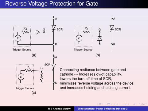
Reverse Voltage Protection for Gate
A
K
G
Trigger Source
SCR
Connecting resitance between gate andcathode --- Increases dv/dt capability,lowers the turn off time of SCR,minimizes reverse voltage across the device,and increases holding and latching current.
(a) (b)
(c)
A
K
G
Trigger Source
SCR
A
K
G
Trigger Source
SCR
R S Ananda Murthy Semiconductor Power Switching Devices-2
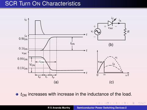
SCR Turn ON Characteristics
(a)
(b)
(c)
tON increases with increase in the inductance of the load.
R S Ananda Murthy Semiconductor Power Switching Devices-2
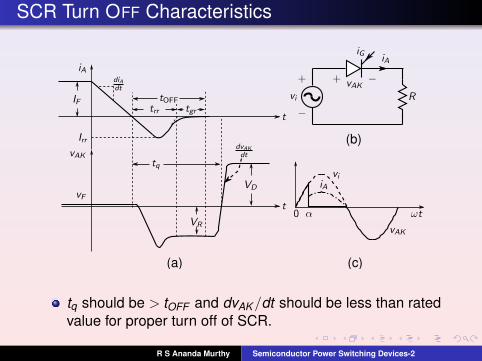
SCR Turn OFF Characteristics
(a)
(b)
(c)
tq should be > tOFF and dvAK/dt should be less than ratedvalue for proper turn off of SCR.
R S Ananda Murthy Semiconductor Power Switching Devices-2
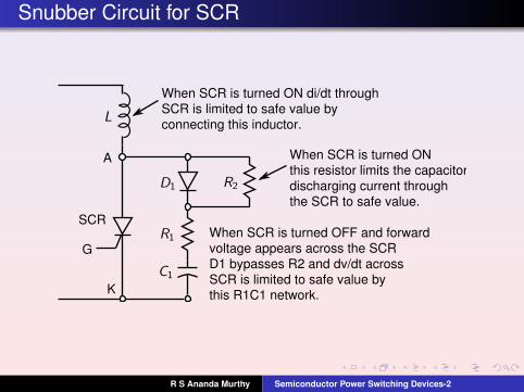
Snubber Circuit for SCR
When SCR is turned ON di/dt throughSCR is limited to safe value byconnecting this inductor.
When SCR is turned ONthis resistor limits the capacitordischarging current throughthe SCR to safe value.
When SCR is turned OFF and forwardvoltage appears across the SCRD1 bypasses R2 and dv/dt acrossSCR is limited to safe value bythis R1C1 network.
A
K
SCR
G
R S Ananda Murthy Semiconductor Power Switching Devices-2
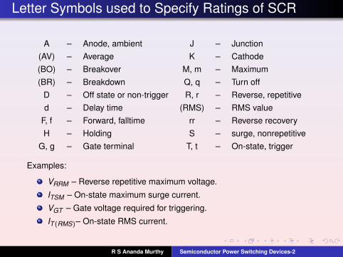
Letter Symbols used to Specify Ratings of SCR
A – Anode, ambient J – Junction(AV) – Average K – Cathode(BO) – Breakover M, m – Maximum(BR) – Breakdown Q, q – Turn off
D – Off state or non-trigger R, r – Reverse, repetitived – Delay time (RMS) – RMS value
F, f – Forward, falltime rr – Reverse recoveryH – Holding S – surge, nonrepetitive
G, g – Gate terminal T, t – On-state, trigger
Examples:
VRRM – Reverse repetitive maximum voltage.
ITSM – On-state maximum surge current.
VGT – Gate voltage required for triggering.
IT (RMS)– On-state RMS current.
R S Ananda Murthy Semiconductor Power Switching Devices-2
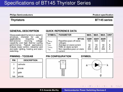
Specifications of BT145 Thyristor Series
R S Ananda Murthy Semiconductor Power Switching Devices-2

Specifications of BT145 Thyristor Series
R S Ananda Murthy Semiconductor Power Switching Devices-2
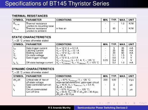
Specifications of BT145 Thyristor Series
R S Ananda Murthy Semiconductor Power Switching Devices-2

Specifications of BT145 Thyristor Series
R S Ananda Murthy Semiconductor Power Switching Devices-2
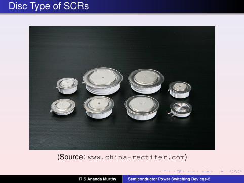
Disc Type of SCRs
(Source: www.china-rectifer.com)
R S Ananda Murthy Semiconductor Power Switching Devices-2

Disc Type of SCR
(Source: www.abb.com)
R S Ananda Murthy Semiconductor Power Switching Devices-2
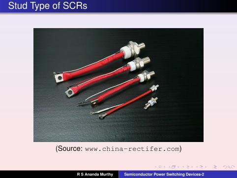
Stud Type of SCRs
(Source: www.china-rectifer.com)
R S Ananda Murthy Semiconductor Power Switching Devices-2
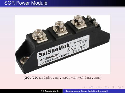
SCR Power Module
(Source: saishe.en.made-in-china.com)
R S Ananda Murthy Semiconductor Power Switching Devices-2
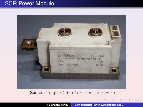
SCR Power Module
(Source: http://theelectrostore.com)
R S Ananda Murthy Semiconductor Power Switching Devices-2
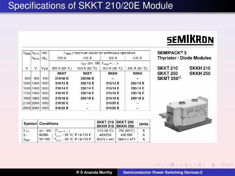
Specifications of SKKT 210/20E Module
R S Ananda Murthy Semiconductor Power Switching Devices-2

Specifications of SKKT 210/20E Module
R S Ananda Murthy Semiconductor Power Switching Devices-2
Next Lecture...
In the next lecture we will discuss some more powersemiconductor switching devices used in power electronics.
Thank You.
R S Ananda Murthy Semiconductor Power Switching Devices-2
Recommended