ISO1176Function Diagram
DE
6D
5
R3
4RE
ISODE10
B
A
13
12
PV7
GA
LV
AN
IC IS
OL
AT
ION
Product
Folder
Sample &Buy
Technical
Documents
Tools &
Software
Support &Community
ISO1176SLLS897E –MARCH 2008–REVISED JUNE 2015
ISO1176 Isolated RS-485 Profibus Transceiver1 Features 3 Description
The ISO1176 device is an isolated differential line1• Meets or Exceeds the Requirements of
transceiver designed for use in PROFIBUSEN 50170 and TIA/EIA-485-Aapplications. The device is ideal for long transmission
• Signaling Rates up to 40 Mbps lines because the ground loop is broken to provide for• Differential Output Exceeds 2.1 V (54-Ω Load) operation with a much larger common-mode voltage
range. The symmetrical isolation barrier of each• Low Bus Capacitance – 10 pF (Maximum)device is tested to provide 2500 VRMS of isolation per• Up to 160 Transceivers on a Bus UL between the line transceiver and the logic level
• 50 kV/μs Typical Transient Immunity interface.• Fail-Safe Receiver for Bus Open, Short, Idle The galvanically isolated differential bus transceiver is• 3.3-V Inputs are 5-V Tolerant an integrated circuit designed for bidirectional data
communication on multipoint bus-transmission lines.• Bus-Pin ESD ProtectionThe transceiver combines a galvanically isolated– 16-kV HBM Between Bus Pins and GND2 differential line driver and differential input line
– 6-kV HBM Between Bus Pins and GND1 receiver. The driver has an active-high enable withisolated enable-state output on the ISODE pin (pin• Safety and Regulatory Approvals10) to facilitate direction control. The driver differential– 4000-VPK Isolation, 560-VPK VIORM per DIN Voutputs and the receiver differential inputs connectVDE V 0884-10 (VDE V 0884-10): 2006-12 internally to form a differential input/output (I/O) busand DIN EN 61010-1 port that is designed to offer minimum loading to the
– 2500 VRMS Isolation Rating per UL 1577 bus allowing up to 160 nodes.– 4000 VPK Isolation Rating per CSA CA5A and The PV pin (pin 7) is provided as a full-chip enable
IEC 60950-1 option. All device outputs become high impedancewhen a logic low is applied to the PV pin. For more
2 Applications information, see the function tables in DeviceFunctional Modes.• Profibus
• Factory Automation Device Information(1)
• Networked Sensors PART NUMBER PACKAGE BODY SIZE (NOM)• Motor and Motion Control ISO1176 SOIC (16) 10.30 mm × 7.50 mm• HVA and Building Automation Networks (1) For all available packages, see the orderable addendum at
the end of the data sheet.• Networked Security Stations
Simplified Schematic
1
An IMPORTANT NOTICE at the end of this data sheet addresses availability, warranty, changes, use in safety-critical applications,intellectual property matters and other important disclaimers. PRODUCTION DATA.
ISO1176SLLS897E –MARCH 2008–REVISED JUNE 2015 www.ti.com
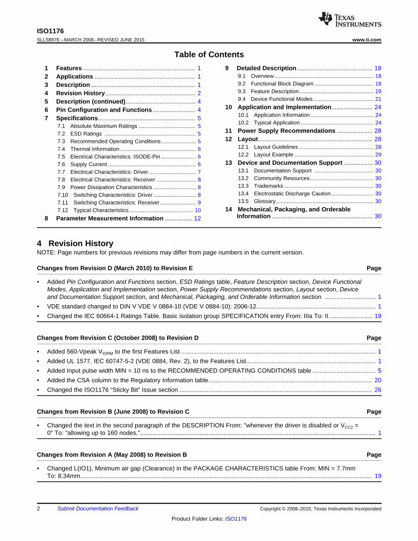
Table of Contents1 Features .................................................................. 1 9 Detailed Description ............................................ 18
9.1 Overview ................................................................. 182 Applications ........................................................... 19.2 Functional Block Diagram ....................................... 183 Description ............................................................. 19.3 Feature Description................................................. 194 Revision History..................................................... 29.4 Device Functional Modes........................................ 215 Description (continued)......................................... 4
10 Application and Implementation........................ 246 Pin Configuration and Functions ......................... 410.1 Application Information.......................................... 247 Specifications......................................................... 510.2 Typical Application ................................................ 247.1 Absolute Maximum Ratings ...................................... 5
11 Power Supply Recommendations ..................... 287.2 ESD Ratings ............................................................ 512 Layout................................................................... 287.3 Recommended Operating Conditions....................... 5
12.1 Layout Guidelines ................................................. 287.4 Thermal Information .................................................. 612.2 Layout Example .................................................... 297.5 Electrical Characteristics: ISODE-Pin ....................... 6
13 Device and Documentation Support ................. 307.6 Supply Current .......................................................... 613.1 Documentation Support ....................................... 307.7 Electrical Characteristics: Driver ............................... 713.2 Community Resources.......................................... 307.8 Electrical Characteristics: Receiver .......................... 813.3 Trademarks ........................................................... 307.9 Power Dissipation Characteristics ............................ 813.4 Electrostatic Discharge Caution............................ 307.10 Switching Characteristics: Driver ............................ 813.5 Glossary ................................................................ 307.11 Switching Characteristics: Receiver........................ 9
14 Mechanical, Packaging, and Orderable7.12 Typical Characteristics .......................................... 10Information ........................................................... 308 Parameter Measurement Information ................ 12
4 Revision HistoryNOTE: Page numbers for previous revisions may differ from page numbers in the current version.
Changes from Revision D (March 2010) to Revision E Page
• Added Pin Configuration and Functions section, ESD Ratings table, Feature Description section, Device FunctionalModes, Application and Implementation section, Power Supply Recommendations section, Layout section, Deviceand Documentation Support section, and Mechanical, Packaging, and Orderable Information section .............................. 1
• VDE standard changed to DIN V VDE V 0884-10 (VDE V 0884-10): 2006-12...................................................................... 1• Changed the IEC 60664-1 Ratings Table. Basic isolation group SPECIFICATION entry From: IIIa To: II ......................... 19
Changes from Revision C (October 2008) to Revision D Page
• Added 560-Vpeak VIORM to the first Features List .................................................................................................................. 1• Added UL 1577, IEC 60747-5-2 (VDE 0884, Rev. 2), to the Features List............................................................................ 1• Added Input pulse width MIN = 10 ns to the RECOMMENDED OPERATING CONDITIONS table ..................................... 5• Added the CSA column to the Regulatory Information table................................................................................................ 20• Changed the ISO1176 “Sticky Bit” Issue section ................................................................................................................. 26
Changes from Revision B (June 2008) to Revision C Page
• Changed the text in the second paragraph of the DESCRIPTION From: "whenever the driver is disabled or VCC2 =0" To: "allowing up to 160 nodes.".......................................................................................................................................... 1
Changes from Revision A (May 2008) to Revision B Page
• Changed L(IO1), Minimum air gap (Clearance) in the PACKAGE CHARACTERISTICS table From: MIN = 7.7mmTo: 8.34mm........................................................................................................................................................................... 19
2 Submit Documentation Feedback Copyright © 2008–2015, Texas Instruments Incorporated
Product Folder Links: ISO1176

ISO1176www.ti.com SLLS897E –MARCH 2008–REVISED JUNE 2015
Changes from Original (March 2008) to Revision A Page
• Added 3.3-V Inputs are 5-V Tolerant to the Features List...................................................................................................... 1• Added the Bus-Pin ESD Protection bullet and sub bullets to the Features List..................................................................... 1• Added Bus pins to GND1 and Bus pins to GND2 to the ESD information in the Handling Rating table ............................... 5• Added the APPLICATION INFORMATION section.............................................................................................................. 24
Copyright © 2008–2015, Texas Instruments Incorporated Submit Documentation Feedback 3
Product Folder Links: ISO1176
1
2
3
4
5
6
7
8 9
10
11
12
13
14
15
16
R
RE
D
GND1
NC
VCC2
B
A
NC
GND2
DE
VCC1
GND1 GND2
ISODEPV
ISO1176SLLS897E –MARCH 2008–REVISED JUNE 2015 www.ti.com
5 Description (continued)Any cabled I/O can be subjected to electrical noise transients from various sources. These noise transients cancause damage to the transceiver and/or nearby sensitive circuitry if they are of sufficient magnitude and duration.The ISO1176 can significantly reduce the risk of data corruption and damage to expensive control circuits.
The device is characterized for operation over the ambient temperature range of –40°C to +85°C.
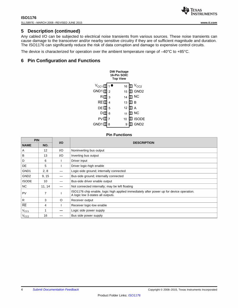
6 Pin Configuration and Functions
DW Package16-Pin SOIC
Top View
Pin FunctionsPIN
I/O DESCRIPTIONNAME NO.A 12 I/O Noninverting bus outputB 13 I/O Inverting bus outputD 6 I Driver inputDE 5 I Driver logic-high enableGND1 2, 8 — Logic-side ground; internally connectedGND2 9, 15 — Bus-side ground; internally connectedISODE 10 — Bus-side driver enable outputNC 11, 14 — Not connected internally; may be left floating
ISO1176 chip enable, logic high applied immediately after power up for device operation.PV 7 I A logic low 3-states all outputs.R 3 O Receiver outputRE 4 I Receiver logic-low enableVCC1 1 — Logic side power supplyVCC2 16 — Bus side power supply
4 Submit Documentation Feedback Copyright © 2008–2015, Texas Instruments Incorporated
Product Folder Links: ISO1176

ISO1176www.ti.com SLLS897E –MARCH 2008–REVISED JUNE 2015
7 Specifications
7.1 Absolute Maximum Ratingsover operating junction temperature range unless otherwise noted (1)
MIN MAX UNITVCC Supply voltage (2) VCC1, VCC2 –0.5 7 VVO Voltage at any bus I/O pins –9 14 VVI Voltage input D, DE or RE –0.5 7 VIO Receiver output current –10 10 mATJ Maximum junction temperature 170 °CTstg Storage temperature -65 150 °C
(1) Stresses beyond those listed under Absolute Maximum Ratings may cause permanent damage to the device. These are stress ratingsonly, and functional operation of the device at these or any other conditions beyond those indicated under Recommended OperatingConditions is not implied. Exposure to absolute-maximum-rated conditions for extended periods may affect device reliability. All voltagevalues are with respect to the network ground terminal unless otherwise noted.
(2) All voltage values except differential I/O bus voltages are with respect to the referenced network ground terminal and are peak voltagevalues.
7.2 ESD RatingsVALUE UNIT
Human body model (HBM), per ANSI/ESDA/JEDEC JS- Bus pins to 2, 8 ±6000001 (1)
Bus pins to 9, 15 ±16000ElectrostaticV(ESD) All pins ±4000 Vdischarge
Charged device model (CDM), per JEDEC specification JESD22-C101, all pins (2) ±1000Machine model (MM), per ANSI/ESDS5.2-1996, all pins ±200
(1) JEDEC document JEP155 states that 500-V HBM allows safe manufacturing with a standard ESD control process.(2) JEDEC document JEP157 states that 250-V CDM allows safe manufacturing with a standard ESD control process.
7.3 Recommended Operating ConditionsMIN NOM MAX UNIT
Logic-side supply voltage, VCC1 (with respect to GND1) 3.15 5.5VCC V
Bus-side supply voltage, VCC2 (with respect to GND2) 4.75 5.25VCM Voltage at either bus I/O terminal A, B –7 12 V
PV, RE 2 5.5VIH High-level input voltage V
D, DE 0.7 VCC1
PV, RE 0 0.8VIL Low-level input voltage V
D, DE 0.3 VCC1
VID Differential input voltage A with respect to B –12 12 VDriver –70 70
IO Output current mAReceiver –8 8
Input pulse width 10 nsTA Ambient temperature –40 25 85 °CTJ Junction temperature 150 °C
Copyright © 2008–2015, Texas Instruments Incorporated Submit Documentation Feedback 5
Product Folder Links: ISO1176
ISO1176SLLS897E –MARCH 2008–REVISED JUNE 2015 www.ti.com
7.4 Thermal InformationISO1176
THERMAL METRIC (1) DW [SOIC] UNIT16 PINS
High-K board 81.4RθJA Junction-to-ambient thermal resistance °C/W
Low-K board 168RθJC(top) Junction-to-case (top) thermal resistance 41.4 °C/WRθJB Junction-to-board thermal resistance 46.4 °C/WψJT Junction-to-top characterization parameter 13.1 °C/WψJB Junction-to-board characterization parameter 45.8 °C/WRθJC(bot) Junction-to-case (bottom) thermal resistance N/A °C/W
(1) For more information about traditional and new thermal metrics, see the Semiconductor and IC Package Thermal Metrics applicationreport, SPRA953.
7.5 Electrical Characteristics: ISODE-Pinover recommended operating conditions (unless otherwise noted)
PARAMETER TEST CONDITIONS MIN TYP MAX UNITIOH = –8 mA VCC2 – 0.8 4.6
VOH High-level output voltage VIOH = –20 μA VCC2 – 0.1 5IOL = 8 mA 0.2 0.4
VOL Low-level output voltage VIOL = 20 μA 0 0.1
7.6 Supply Currentover recommended operating conditions (unless otherwise noted)
PARAMETER TEST CONDITIONS MIN TYP MAX UNITDE at 0 V 4 6
3 V DE at VCC1, 2 Mbps 5DE at VCC1, 25 Mbps 6
ICC1 Logic-side RMS supply current mADE at 0 V 7 10
5.5 V DE at VCC1, 2 Mbps 8DE at VCC1, 25 Mbps 11DE at 0 V 15 18
ICC2 Bus-side RMS supply current 5.25 V DE at VCC1, 2 Mbps, 54-Ω load 70 mADE at VCC1, 25 Mbps, 54-Ω load 75
6 Submit Documentation Feedback Copyright © 2008–2015, Texas Instruments Incorporated
Product Folder Links: ISO1176
ISO1176www.ti.com SLLS897E –MARCH 2008–REVISED JUNE 2015
7.7 Electrical Characteristics: Driverover recommended operating conditions (unless otherwise noted)
PARAMETER TEST CONDITIONS MIN TYP MAX UNITVOD Open-circuit differential output voltage |VA – VB|, Figure 8 1.5 VCC2 V
See Figure 9 and Figure 13 2.1Steady-state differential output voltage|VOD(SS)| VCommon-mode loading with Vtest from –7magnitude 2.1V to 12 V, See Figure 10Change in steady-state differential output|ΔVOD(SS)| RL = 54 Ω, See Figure 11 and Figure 12 –0.2 0.2 Vvoltage between logic states
VOC(SS) Steady-state common-mode output voltage 2 3Change in steady-state common-mode outputΔVOC(SS) RL = 54 Ω, See Figure 11 and Figure 12 –0.2 0.2 Vvoltage
VOC(PP) Peak-to-peak common-mode output voltage 0.5Differential output voltage over- andVOD(RING) See Figure 13 and Figure 17 10% VOD(pp)undershoot
VI(HYS) Input voltage hysteresis See Figure 14 150 mVD, DE at 0 V or VCC1 –10 10
II Input current μAPV (1) at 0 V or VCC1 120
IO(OFF) Output current with power off VCC ≤ 2.5 V See receiver inputcurrent in Electrical
Characteristics:IOZ High-impedance state output current DE at 0 VReceiver
IOS(P) Peak short-circuit output current VOS = –7 V to 12 V –250 250DE at VCC, See VOS = 12 V, D at 135Figure 15 and GND1 mA
IOS(SS) Steady-state short-circuit output current Figure 16 VOS = –7 V, D at –135VCC1
See receiver CIN inElectricalCOD Differential output capacitance Characteristics:Receiver
CMTI Common-mode transient immunity See Figure 27 25 kV/μs
(1) The PV pin has a 50-kΩ pullup resistor and leakage current depends on supply voltage.
Copyright © 2008–2015, Texas Instruments Incorporated Submit Documentation Feedback 7
Product Folder Links: ISO1176
ISO1176SLLS897E –MARCH 2008–REVISED JUNE 2015 www.ti.com
7.8 Electrical Characteristics: Receiverover recommended operating conditions (unless otherwise noted)
PARAMETER TEST CONDITIONS MIN TYP MAX UNIT
VIT(+) Positive-going differential input voltage threshold IO = –8 mA –80 –10 mVSeeFigure 22
VIT(–) Negative-going differential input voltage threshold IO = 8 mA –200 –120 mV
Vhys Hysteresis voltage (VIT+ – VIT-) 40 mV
IOH = –8 mA VCC1 –0.4 3VID = 200 mV,VOH High-level output voltage VSee Figure 22 IO H = –20 μA VCC1 –0.1 3.3VCC1 at 3.3 V and VCC2 at5 V IO L = 8 mA 0.2 0.4VID = –200 mV,VOL Low-level output voltage VSee Figure 22 IOL = 20 μA 0 0.1
IOH = –8 mA VCC1 –0.8 4.6VID = 200 mV,VOH High-level output voltage VSee Figure 22 IO H = –20 μA VCC1 –0.1 5VCC1 at 5 V and VCC2 at 5V IO L = 8 mA 0.2 0.4VID = –200 mV,VOL Low-level output voltage VSee Figure 22 IOL = –20 μA 0 0.1
IA, IB VCC = 4.75 V or 5.25 VVI = –7 V or 12 V,Bus pin input current –160 200 μAIA(OFF) Other input = 0 V VCC2 = 0 VIB(OFF)
II Receiver enable input current RE = 0 V –50 50 μA
IOZ High-impedance state output current RE = VCC1 –1 1 μA
RID Differential input resistance A, B 48 kΩ
Test input signal is a 1.5-MHz sine wave with1 Vpp amplitude , CD is measured acrossCID Differential input capacitance 7 10 pFA and B
CMR Common-mode rejection See Figure 26 4 V
7.9 Power Dissipation CharacteristicsPARAMETER VALUE UNIT
VCC1 = VCC2 = 5.25 V, TJ = 150°C, CL = 15 pF,PD Power Dissipation 220 mWInput a 20 MHz 50% duty-cycle square wave
7.10 Switching Characteristics: Driverover recommended operating conditions (unless otherwise noted)
PARAMETER TEST CONDITIONS MIN TYP MAX UNITtpLH, tpHL Propagation delay time 35 nsVCC1 at 5 V
VCC2 at 5 Vtsk(p) Pulse skew (|tp HL – tpLH|) 2 5 nstpLH, tpHL Propagation delay time 40 nsVCC1 at 3.3 V See Figure 17VCC2 at 5 Vtsk(p) Pulse skew (|tp HL – tp LH|) 2 5 nstr Differential output signal rise time 2 3 7.5 nstf Differential output signal fall time 2 3 7.5 nstpDE DE to ISODE prop delay See Figure 21 30 nstt(MLH), tt(MHL) Output transition skew See Figure 18 1 nstp(AZH), tp(BZH) Propagation delay time, high-impedance-to-active output 80 nstp(AZL), tp(BZL) CL = 50 pF,tp(AHZ), tp(BHZ) RE at 0 V,Propagation delay time, active-to-high-impedance output 80 nstp(ALZ), tp(BLZ) See Figure 19 and
Figure 20|tp(AZL) – tp(BZH)| Enable skew time 0.55 1.5 ns|tp(AZH) – tp(BZL)|t(CFB) Time from application of short-circuit to current foldback See Figure 16 0.5 μst(TSD) Time from application of short-circuit to thermal shutdown TA = 25°C, See Figure 16 100 μs
8 Submit Documentation Feedback Copyright © 2008–2015, Texas Instruments Incorporated
Product Folder Links: ISO1176

ISO1176www.ti.com SLLS897E –MARCH 2008–REVISED JUNE 2015
7.11 Switching Characteristics: Receiverover recommended operating conditions (unless otherwise noted)
PARAMETER TEST CONDITIONS MIN TYP MAX UNITtpLH, tpHL Propagation delay time 50 ns
VCC1 at 5 V, VCC2 at 5 Vtsk(p) Pulse skew (|tp HL – tpLH|) 2 5 nstpLH, tpHL Propagation delay time 55 ns
VCC1 at 3.3 V, VCC2 at 5 V See Figure 23tsk(p) Pulse skew (|tp HL – tp LH|) 2 5 nstr Output signal rise time 2 4 nstf Output signal fall time 2 4 nstpZH Propagation delay time, high-impedance-to-high-level output 13 25 nsDE at VCC1,
See Figure 24tpHZ Propagation delay time, high-level-to-high-impedance output 13 25 nstpZL Propagation delay time, high-impedance-to-low-level output 13 25 nsDE at VCC,
See Figure 25tpLZ Propagation delay time, low-level-to-high-impedance output 13 25 ns
Copyright © 2008–2015, Texas Instruments Incorporated Submit Documentation Feedback 9
Product Folder Links: ISO1176

-99
-89
-79
-69
-59
-49
-39
-29
-19
-9
10 1 2 3 4 5
V - Output Voltage - VO
I-
Ou
tpu
t C
urr
en
t -
mA
O
15 pF LoadT = 25°CA
0
0.1
0.2
0.3
0.4
0.5
0.6
0.7
−40 −15 10 35 60 85
VCC = 4.75 V
VCC = 5.25 V
TA − Free-Air Temperature −°C
Dri
ver
En
ab
le S
kew
−n
s
RL = 110 Ω,
CL = 50 pF
VCC = 5 V
2
2.25
2.5
2.75
3
3.25
3.5
3.75
4
−40 −15 10 35 60 85
VCC = 4.75 V
VCC = 5.25 V
VCC = 5 V
Dri
ver
Ris
e, F
all T
ime
−n
s
TA − Free-Air Temperature −°C
RL = 54 Ω,
CL = 50 pF
0
0.05
0.1
0.15
0.2
0.25
0.3
0.35
−40 −15 10 35 60 85
VCC = 4.75 V
VCC = 5 V
VCC = 5.25 V
Dri
ver
Ou
tpu
t Tr
an
sit
ion
Skew
−n
s
TA − Free-Air Temperature −°C
RL = 54 Ω,
CL = 50 pF
0
10
20
30
40
50
60
70
80
90
100
0 5 10 15 20
Signalling Rate - Mbps
I-
Su
pp
ly C
urr
en
t -
mA
CC
ICC1
ICC2
5 V VCC1
3.3 V VCC1
No LoadT = 25°CA
0
0.5
1
1.5
2
2.5
3
3.5
4
4.5
5
0 20 40 60 80
VCC = 4.75 V
VCC = 5 V
VCC = 5.25 V
VO
D−
Dif
fere
nti
al O
utp
ut
Volt
ag
e−
V
IL − Load Current − mA
100 Ω
50 Ω
TA = 25 C
ISO1176SLLS897E –MARCH 2008–REVISED JUNE 2015 www.ti.com
7.12 Typical Characteristics
Figure 1. Differential Output Voltage vs Load Current Figure 2. RMS Supply Current vs Signaling Rate
Figure 3. Driver Output Transition Skew vs Free-Air Figure 4. Driver Rise and Fall Time vs Free-Air TemperatureTemperature
Figure 5. Driver Enable Skew vs Free-Air Temperature Figure 6. High-Level Output Voltage vs High-Level OutputCurrent
10 Submit Documentation Feedback Copyright © 2008–2015, Texas Instruments Incorporated
Product Folder Links: ISO1176
0
10
20
30
40
50
60
70
80
90
100
110
0 1 2 3 4 5
V - Output Voltage - VO
I-
Ou
tpu
t C
urr
en
t -
mA
O
15 pF LoadT = 25°CA
ISO1176www.ti.com SLLS897E –MARCH 2008–REVISED JUNE 2015
Typical Characteristics (continued)
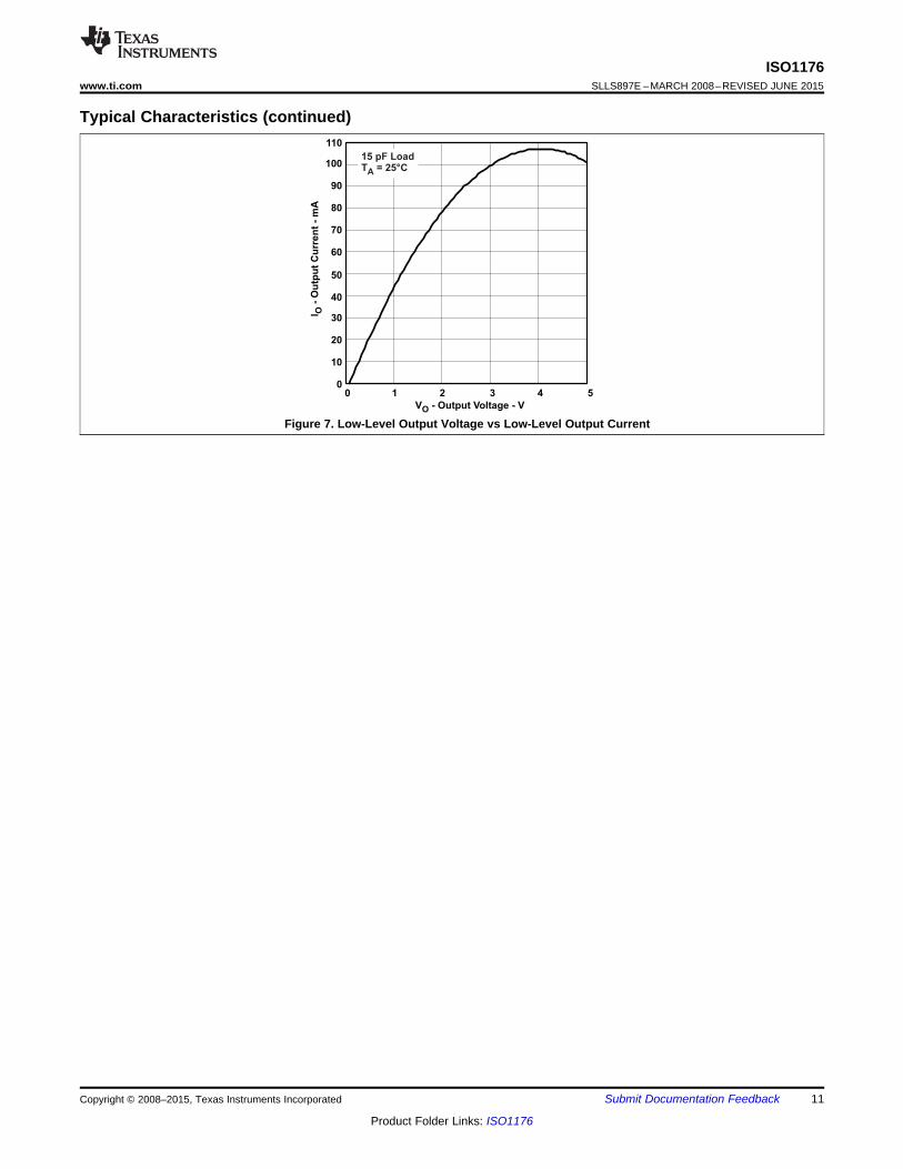
Figure 7. Low-Level Output Voltage vs Low-Level Output Current
Copyright © 2008–2015, Texas Instruments Incorporated Submit Documentation Feedback 11
Product Folder Links: ISO1176
375 W
60 W
+
VOD-
D
DE
GND 2
A
B0 or 3 V
VCC2
375 W
-7 V
to
12 V
I I
VI
D
DE
A
B
VOB VOA
VOD
IOA
IOB
GND 1
GND 1 GND 2
54 W
VCC1
0 or
VCC1
GND 2
I
VI
D
DE
A
B
VOB VOA
VOD
IOA
IOB
GND 1
GND 2
VCC1
0 or
VCC1
GND 1
GND 2
ISO1176SLLS897E –MARCH 2008–REVISED JUNE 2015 www.ti.com
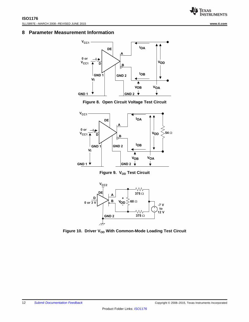
8 Parameter Measurement Information
Figure 8. Open Circuit Voltage Test Circuit
Figure 9. VOD Test Circuit
Figure 10. Driver VOD With Common-Mode Loading Test Circuit
12 Submit Documentation Feedback Copyright © 2008–2015, Texas Instruments Incorporated
Product Folder Links: ISO1176

0 V Differential
VOD(pp)
VDO(RING)
VDO(SS)
Generator PRR = 500 kHz,50% duty cycle, t < 6 ns,
t < 6 ns, Z = 50r
t O Ω
II
VI
D
DEA
B
VOB VOA
VOD
IOA
IOB
GND 1
VOC
RL2
RL2
VOC
B VB
VAA
OC(p-p)V
VOC(SS)
VCC1
GND 1 GND 2
GND 2
Input
II
VI
D
DE
A
B
VOB VOA
VOD
IOA
IOB
GND 1
GND 1 GND 2
VOC
RL
2
RL
2
VCC1
0 or
VCC1
GND 2
ISO1176www.ti.com SLLS897E –MARCH 2008–REVISED JUNE 2015
Parameter Measurement Information (continued)
Figure 11. Driver VOD and VOC Without Common-Mode Loading Test Circuit
Figure 12. Steady-State Output Voltage Test Circuit and Voltage Waveforms
Figure 13. VOD(RING) Waveform and Definitions
Copyright © 2008–2015, Texas Instruments Incorporated Submit Documentation Feedback 13
Product Folder Links: ISO1176

VOD
50 W
D
A
B
DE
VIInput
Generator
90%GND 1
VCC1
R = 54
±1%L W
C = 50 pF
± 20%L
C Includes Fixture and
Instrumentation CapacitanceL
Generator PRR = 500 kHz, 50 % Duty
Cycle, t <6 ns, Z = 50r O W
VI
VOD
3 V
1.5 V 1.5 V
tPLHtPHL
VOD (H)
VOD (L)
90%
0 V 0 V
10% 10%
trtf
IOS
D
A
B
Vos
IOS
time
60
250
120
GND 2GND 1
DE
GND 2 t(CFB)
t(TSD)
Ou
tpu
t C
urr
en
t -
mA
I OS
D
A
B
Vos
I OS
time
60
250
120
GND 1
DE
GND 2GND 2
0.5 W
t(CFB)
t(TSD)
Ou
tpu
t C
urr
en
t -
mA
II
VI
D
DE
A
B
VOB VOA
VOD
IOA
IOBGND 1
54 W
VCC1
0 or
VCC1
GND 1
GND 2
GND 2
ISO1176SLLS897E –MARCH 2008–REVISED JUNE 2015 www.ti.com
Parameter Measurement Information (continued)
Figure 14. Input Voltage Hysteresis Test Circuit
Figure 15. Driver Short-Circuit Test Circuit and Waveforms (Short-Circuit Applied at Time t=0)
Figure 16. IOS(SS) Steady State Short-Circuit Output Current Test Circuit
Figure 17. Driver Switching Test Circuit and Waveforms
14 Submit Documentation Feedback Copyright © 2008–2015, Texas Instruments Incorporated
Product Folder Links: ISO1176

Signal
Generator
DE
B
A
D
VOA VOB
DE
A
B
50%
0 V
50 W
GND 1 GND 2
R = 110L W
C = 50 pFL
R = 110L W
C = 50 pFL
VCC2
t(AZH)
t(BZL)
1.5 V
V +0.5 VOL
V -0.5 VOH
V = 3 VIN t(AHZ)
50%
t(BLZ)
Generator PRR = 500 kHz, 50% Duty
Cycle, t <6 ns, t <6 ns, Z = 50r f O W
DE
A
B
50 %
50 %
0 V
Signal
Generator 50 W
DE
B
A
D
GND 1 GND 2
VOAVOB
V = 0 VIN
R = 110L W
C = 50 pFL
R = 110L W
C = 50 pFL
VCC2
t(AZL)
t(BZH)
1.5 V
t(ALZ)
t(BHZ)
V +0.5 VOL
V -0.5 VO
Generator PRR = 500 kHz, 50% Duty
Cycle, t <6 ns, t <6 ns, Z = 50r f O W
50 W
D
A
B
DE
VIInput
Generator
GND 1 VOA VOB
50 %
VO
A
B
VCC1
GND 2
R = 54
±1%L W C = 50 pF
±20%L tt(MHL) tt(MLH)
50 %
50 % 50 %
C Includes Fixture and
Instrumentation CapacitanceL
Generator PRR = 500 kHz, 50% Duty
Cycle, t <6 ns, t <6 ns, Z = 50r f O W
ISO1176www.ti.com SLLS897E –MARCH 2008–REVISED JUNE 2015
Parameter Measurement Information (continued)
Figure 18. Driver Output Transition Skew Test Circuit and Waveforms
Figure 19. Driver Enable and Disable Test, D at Logic Low Test Circuit and Waveforms
Figure 20. Driver Enable and Disable Test, D at Logic High Test Circuit and Waveforms
Copyright © 2008–2015, Texas Instruments Incorporated Submit Documentation Feedback 15
Product Folder Links: ISO1176

1.5 V
VO
GND
tpZH tpHZ
1.5 V
3 V
0 V
1.5 V
RE
R
SignalGenerator
50 W
CL= 15 pF
R
A
B
1 kW
RE
PRR = 100 kHz, 50% duty cycle,
t <6 ns, t <6 ns, Z = 50r f O W
(Includes Probe andJig Capacitance)
DE
D
54 W
0 V
VCC
VCC
V -0.5 VOH
Input A
Output
50%
VOH
VOLtftr
tpLH tpHL
10%
90%
1.5 V
1.5 V
0 V
Input BSignal
Generator 50 W
CL= 15 pF
R
A
B
VID
VO
IO
(Includes Probe andJig Capacitance)
PRR = 100 kHz, 50% Duty Cycle,
t <6 ns, t <6 ns, Z = 50r f O W
SignalGenerator
50 W
VID
IO
VO
SignalGenerator 50 W
DE
D
GND 1
ISODE
ISODE
DE 50%
VCC1 VCC2
V = VIN CC1
GND 2
C = 15 pF
± 20%L
50%
t DE_LHPt DE_HLP
50%
50%
Generator PRR = 500 kHz, 50% Duty
Cycle, t <6 ns, t <6 ns, Z = 50r f O W
ISO1176SLLS897E –MARCH 2008–REVISED JUNE 2015 www.ti.com
Parameter Measurement Information (continued)
Figure 21. DE to ISODE Prop Delay Test Circuit and Waveforms
Figure 22. Receiver DC Parameter Definitions
Figure 23. Receiver Switching Test Circuit and Waveforms
Figure 24. Receiver Enable Test Circuit and Waveforms, Data Output High
16 Submit Documentation Feedback Copyright © 2008–2015, Texas Instruments Incorporated
Product Folder Links: ISO1176

D
R
DE
1 kWRE
54 W
GND 1
VTEST
GND 2
(Includes Probe andJig Capacitance)
A
B
GND1
S1
2 V C = 0.1 F±1%
m VCC1 VCC2
0.8 V
V or VOH OL
C = 15 pFL
Success / Fail Criterion:Stable V or V OutputsOH OL
V or VOH OL
C = 0.1 F ± 1%m
50 W
470 nF100 nF
2.2 kW
Scope
ScopeVR
100 nF
GND
A
B
R
D
RE
DE
V
f = 1 to 50 MHzAmpl. = ± 5 V
INPUT
V
= -2 V to 7 VOFFSET
VCC
50 W
2.2 kW
1.5 V
OHV
VOL
tpZL tpLZ
1.5 V
3 V
0 V
RE
R
1.5 V
0 V
SignalGenerator
R
A
B
RE
DE
D
54 W
50 W
1 kW
PRR = 100 kHz, 50% duty cycle,
t <6 ns, t <6 ns, Z = 50r f O W
CL= 15 pF
(Includes Probe andJig Capacitance)
VCC
VCC1
V +0.5 VOL
ISO1176www.ti.com SLLS897E –MARCH 2008–REVISED JUNE 2015
Parameter Measurement Information (continued)
Figure 25. Receiver Enable Test Circuit and Waveforms, Data Output Low
Figure 26. Common-Mode Rejection Test Circuit
Figure 27. Common-Mode Transient Immunity Test Circuit
Copyright © 2008–2015, Texas Instruments Incorporated Submit Documentation Feedback 17
Product Folder Links: ISO1176
VCC1
R
D
VCC2
GA
LV
AN
ICIS
OLA
TIO
N
GND1 GND2
B
ARE
DE
PV
ISODE
ISO1176SLLS897E –MARCH 2008–REVISED JUNE 2015 www.ti.com
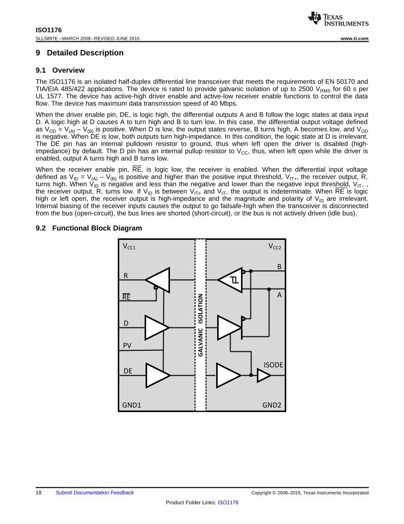
9 Detailed Description
9.1 OverviewThe ISO1176 is an isolated half-duplex differential line transceiver that meets the requirements of EN 50170 andTIA/EIA 485/422 applications. The device is rated to provide galvanic isolation of up to 2500 VRMS for 60 s perUL 1577. The device has active-high driver enable and active-low receiver enable functions to control the dataflow. The device has maximum data transmission speed of 40 Mbps.
When the driver enable pin, DE, is logic high, the differential outputs A and B follow the logic states at data inputD. A logic high at D causes A to turn high and B to turn low. In this case, the differential output voltage definedas VOD = V(A) – V(B) is positive. When D is low, the output states reverse, B turns high, A becomes low, and VODis negative. When DE is low, both outputs turn high-impedance. In this condition, the logic state at D is irrelevant.The DE pin has an internal pulldown resistor to ground, thus when left open the driver is disabled (high-impedance) by default. The D pin has an internal pullup resistor to VCC, thus, when left open while the driver isenabled, output A turns high and B turns low.
When the receiver enable pin, RE, is logic low, the receiver is enabled. When the differential input voltagedefined as VID = V(A) – V(B) is positive and higher than the positive input threshold, VIT+, the receiver output, R,turns high. When VID is negative and less than the negative and lower than the negative input threshold, VIT– ,the receiver output, R, turns low. If VID is between VIT+ and VIT– the output is indeterminate. When RE is logichigh or left open, the receiver output is high-impedance and the magnitude and polarity of VID are irrelevant.Internal biasing of the receiver inputs causes the output to go failsafe-high when the transceiver is disconnectedfrom the bus (open-circuit), the bus lines are shorted (short-circuit), or the bus is not actively driven (idle bus).
9.2 Functional Block Diagram
18 Submit Documentation Feedback Copyright © 2008–2015, Texas Instruments Incorporated
Product Folder Links: ISO1176
ISO1176www.ti.com SLLS897E –MARCH 2008–REVISED JUNE 2015
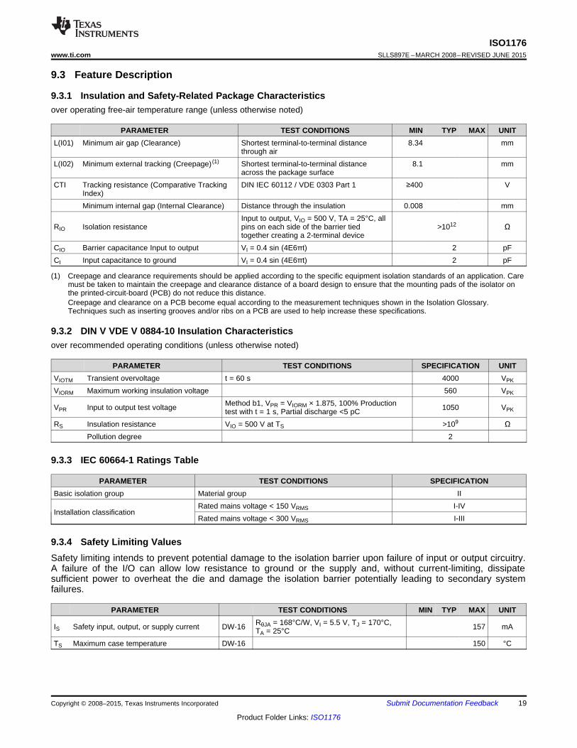
9.3 Feature Description
9.3.1 Insulation and Safety-Related Package Characteristicsover operating free-air temperature range (unless otherwise noted)
PARAMETER TEST CONDITIONS MIN TYP MAX UNITL(I01) Minimum air gap (Clearance) Shortest terminal-to-terminal distance 8.34 mm
through airL(I02) Minimum external tracking (Creepage) (1) Shortest terminal-to-terminal distance 8.1 mm
across the package surfaceCTI Tracking resistance (Comparative Tracking DIN IEC 60112 / VDE 0303 Part 1 ≥400 V
Index)Minimum internal gap (Internal Clearance) Distance through the insulation 0.008 mm
Input to output, VIO = 500 V, TA = 25°C, allRIO Isolation resistance pins on each side of the barrier tied >1012 Ω
together creating a 2-terminal deviceCIO Barrier capacitance Input to output VI = 0.4 sin (4E6πt) 2 pFCI Input capacitance to ground VI = 0.4 sin (4E6πt) 2 pF
(1) Creepage and clearance requirements should be applied according to the specific equipment isolation standards of an application. Caremust be taken to maintain the creepage and clearance distance of a board design to ensure that the mounting pads of the isolator onthe printed-circuit-board (PCB) do not reduce this distance.Creepage and clearance on a PCB become equal according to the measurement techniques shown in the Isolation Glossary.Techniques such as inserting grooves and/or ribs on a PCB are used to help increase these specifications.
9.3.2 DIN V VDE V 0884-10 Insulation Characteristicsover recommended operating conditions (unless otherwise noted)
PARAMETER TEST CONDITIONS SPECIFICATION UNITVIOTM Transient overvoltage t = 60 s 4000 VPK
VIORM Maximum working insulation voltage 560 VPK
Method b1, VPR = VIORM × 1.875, 100% ProductionVPR Input to output test voltage 1050 VPKtest with t = 1 s, Partial discharge <5 pCRS Insulation resistance VIO = 500 V at TS >109 Ω
Pollution degree 2
9.3.3 IEC 60664-1 Ratings Table
PARAMETER TEST CONDITIONS SPECIFICATIONBasic isolation group Material group II
Rated mains voltage < 150 VRMS I-IVInstallation classification
Rated mains voltage < 300 VRMS I-III
9.3.4 Safety Limiting ValuesSafety limiting intends to prevent potential damage to the isolation barrier upon failure of input or output circuitry.A failure of the I/O can allow low resistance to ground or the supply and, without current-limiting, dissipatesufficient power to overheat the die and damage the isolation barrier potentially leading to secondary systemfailures.
PARAMETER TEST CONDITIONS MIN TYP MAX UNITRθJA = 168°C/W, VI = 5.5 V, TJ = 170°C,IS Safety input, output, or supply current DW-16 157 mATA = 25°C
TS Maximum case temperature DW-16 150 °C
Copyright © 2008–2015, Texas Instruments Incorporated Submit Documentation Feedback 19
Product Folder Links: ISO1176
Case Temperature (°C)
Sa
fety
Lim
itin
g C
urr
en
t(m
A)
0 50 100 150 2000
50
100
150
200
D001
VCC1 = VCC2 = 5.5 V
ISO1176SLLS897E –MARCH 2008–REVISED JUNE 2015 www.ti.com
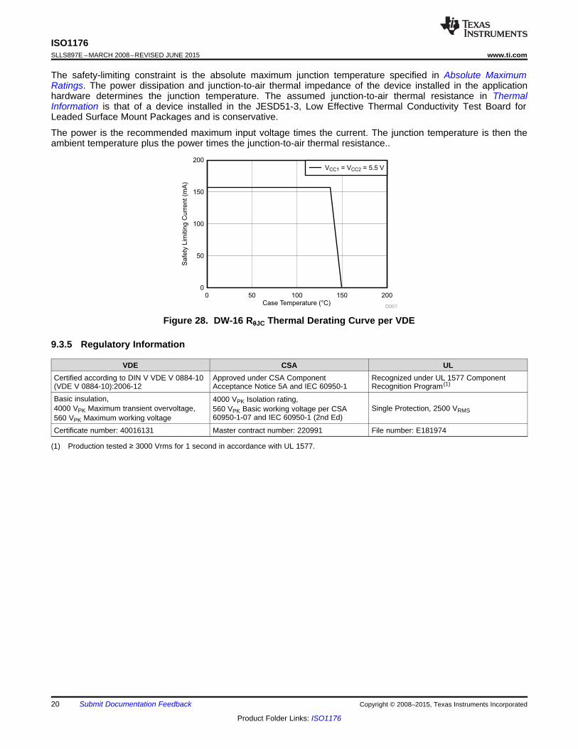
The safety-limiting constraint is the absolute maximum junction temperature specified in Absolute MaximumRatings. The power dissipation and junction-to-air thermal impedance of the device installed in the applicationhardware determines the junction temperature. The assumed junction-to-air thermal resistance in ThermalInformation is that of a device installed in the JESD51-3, Low Effective Thermal Conductivity Test Board forLeaded Surface Mount Packages and is conservative.
The power is the recommended maximum input voltage times the current. The junction temperature is then theambient temperature plus the power times the junction-to-air thermal resistance..
Figure 28. DW-16 RθJC Thermal Derating Curve per VDE
9.3.5 Regulatory Information
VDE CSA ULCertified according to DIN V VDE V 0884-10 Approved under CSA Component Recognized under UL 1577 Component(VDE V 0884-10):2006-12 Acceptance Notice 5A and IEC 60950-1 Recognition Program (1)
Basic insulation, 4000 VPK Isolation rating,4000 VPK Maximum transient overvoltage, Single Protection, 2500 VRMS560 VPK Basic working voltage per CSA
60950-1-07 and IEC 60950-1 (2nd Ed)560 VPK Maximum working voltageCertificate number: 40016131 Master contract number: 220991 File number: E181974
(1) Production tested ≥ 3000 Vrms for 1 second in accordance with UL 1577.
20 Submit Documentation Feedback Copyright © 2008–2015, Texas Instruments Incorporated
Product Folder Links: ISO1176
ISO1176www.ti.com SLLS897E –MARCH 2008–REVISED JUNE 2015
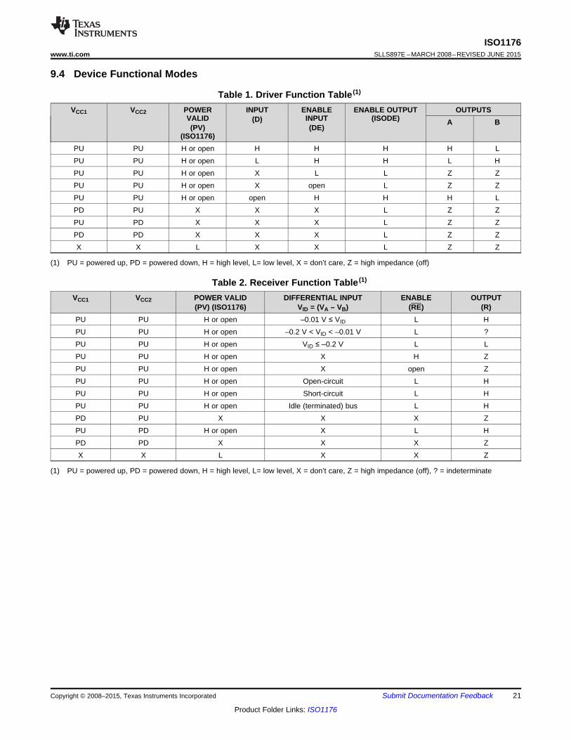
9.4 Device Functional Modes
Table 1. Driver Function Table (1)
VCC1 VCC2 POWER INPUT ENABLE ENABLE OUTPUT OUTPUTSVALID INPUT (ISODE)(D) A B(PV) (DE)
(ISO1176)PU PU H or open H H H H LPU PU H or open L H H L HPU PU H or open X L L Z ZPU PU H or open X open L Z ZPU PU H or open open H H H LPD PU X X X L Z ZPU PD X X X L Z ZPD PD X X X L Z ZX X L X X L Z Z
(1) PU = powered up, PD = powered down, H = high level, L= low level, X = don’t care, Z = high impedance (off)
Table 2. Receiver Function Table (1)
VCC1 VCC2 POWER VALID DIFFERENTIAL INPUT ENABLE OUTPUT(PV) (ISO1176) VID = (VA – VB) (RE) (R)
PU PU H or open –0.01 V ≤ VID L HPU PU H or open –0.2 V < VID < –0.01 V L ?PU PU H or open VID ≤ –0.2 V L LPU PU H or open X H ZPU PU H or open X open ZPU PU H or open Open-circuit L HPU PU H or open Short-circuit L HPU PU H or open Idle (terminated) bus L HPD PU X X X ZPU PD H or open X L HPD PD X X X ZX X L X X Z
(1) PU = powered up, PD = powered down, H = high level, L= low level, X = don’t care, Z = high impedance (off), ? = indeterminate
Copyright © 2008–2015, Texas Instruments Incorporated Submit Documentation Feedback 21
Product Folder Links: ISO1176

500 W
D, RE Input DE Input
PV Input
11 W
ISODE Output
4 W
3.3 V R Output 5 V R Output
VCC1 VCC1 VCC1
500 W
VCC1
1 MW
1 MW
VCC1
VCC2
5.5 W
5.5 W
11 W
VCC1VCC1VCC1
500 W
VCC1
6.4 W
VCC1
50 kW
ISO1176SLLS897E –MARCH 2008–REVISED JUNE 2015 www.ti.com
Figure 29. Equivalent I/O Schematics
22 Submit Documentation Feedback Copyright © 2008–2015, Texas Instruments Incorporated
Product Folder Links: ISO1176
Input
B Input
90 kW
Input
A Input
18 kW16 V
VCC2
16 V 18 kW
16 V
16 V
18 kW
18 kW
VCC2
Output
A and B Outputs
VCC2
16 V
16 V
90 kW
ISO1176www.ti.com SLLS897E –MARCH 2008–REVISED JUNE 2015
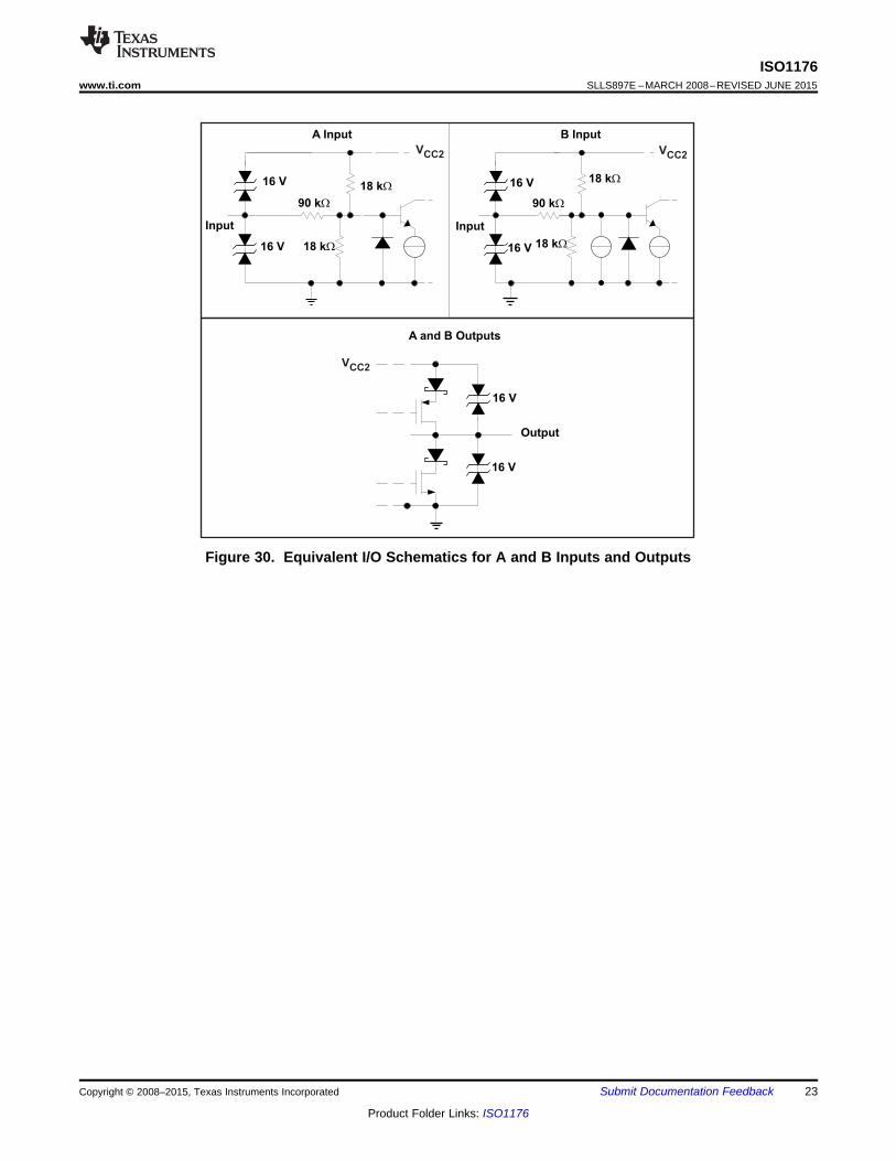
Figure 30. Equivalent I/O Schematics for A and B Inputs and Outputs
Copyright © 2008–2015, Texas Instruments Incorporated Submit Documentation Feedback 23
Product Folder Links: ISO1176

R
D
R
RE
DE
D
A
B
R
D
R
RE
DE
D
A
B
R
D
R
RE
DE
D
A
B
a) Independent driver andreceiver enable signals
b) Combined enable signals foruse as directional control pin
c) Receiver always on
ISO1176SLLS897E –MARCH 2008–REVISED JUNE 2015 www.ti.com
10 Application and Implementation
NOTEInformation in the following applications sections is not part of the TI componentspecification, and TI does not warrant its accuracy or completeness. TI’s customers areresponsible for determining suitability of components for their purposes. Customers shouldvalidate and test their design implementation to confirm system functionality.
10.1 Application InformationThe ISO1176 device consists of a RS-485 transceiver, commonly used for asynchronous data transmissions. Forhalf-duplex transmission, only one pair is shared for both transmission and reception of data. To eliminate linereflections, each cable end is terminated with a termination resistor, R(T), whose value matches thecharacteristic impedance, Z0, of the cable. This method, known as parallel termination, allows for higher datarates over longer cable length.
10.2 Typical Application
Figure 31. Half-Duplex Transceiver Configurations
10.2.1 Design RequirementsRS-485 is a robust electrical standard suitable for long-distance networking that may be used in a wide range ofapplications with varying requirements, such as distance, data rate, and number of nodes.
Table 3. Design ParametersPARAMETER VALUE
Pullup and Pulldown Resistors 1 kΩ to 10 kΩDecoupling Capacitors 100 nF
10.2.2 Detailed Design ProcedureIsolating of a circuit insulates it from other circuits and earth, so that noise voltage develops across the insulationrather than circuit components. The most common noise threat to data-line circuits is voltage surges or electricalfast transients that occur after installation. The transient ratings of the ISO1176 standard are sufficient for all butthe most severe installations. However, some equipment manufacturers use ESD generators to test equipmenttransient susceptibility. This practice can exceed insulation ratings. ESD generators simulate static dischargesthat may occur during device or equipment handling with low-energy but high-voltage transients.
24 Submit Documentation Feedback Copyright © 2008–2015, Texas Instruments Incorporated
Product Folder Links: ISO1176
94.0
1611
1
C
C1
1
C1
C1
C1
v
v
IN
ISO
INISO
ISO
N
2GND=
+
=
+
=
+
=
49
9
INISO
ISO
N
2GND
10x610
10
RR
R
v
v
+
=
+
=
INISO
ISON2GND
ZZ
Zvv
+
=
VN
RINCIN
RISOCISO
System Ground (GND1)
Bus Return (GND2)
16V
A or B
ISO1176www.ti.com SLLS897E –MARCH 2008–REVISED JUNE 2015
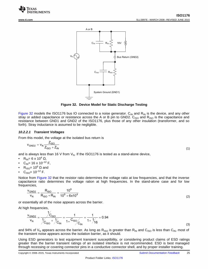
Figure 32. Device Model for Static Discharge Testing
Figure 32 models the ISO1176 bus IO connected to a noise generator. CIN and RIN is the device, and any otherstray or added capacitance or resistance across the A or B pin to GND2. CISO and RISO is the capacitance andresistance between GND1 and GND2 of the ISO1176, plus those of any other insulation (transformer, and soforth). Stray inductance is assumed to be negligible.
10.2.2.1 Transient VoltagesFrom this model, the voltage at the isolated bus return is
(1)
and is always less than 16 V from VN. If the ISO1176 is tested as a stand-alone device,• RIN= 6 x 10⁴ Ω,• CIN= 16 x 10–12 F,• RISO= 109 Ω and• CISO= 10–12 F.
Notice from Figure 32 that the resistor ratio determines the voltage ratio at low frequencies, and that the inversecapacitance ratio determines the voltage ration at high frequencies. In the stand-alone case and for lowfrequencies,
(2)
or essentially all of the noise appears across the barrier.
At high frequencies,
(3)
and 94% of VN appears across the barrier. As long as RISO is greater than RIN and CISO is less than CIN, most ofthe transient noise appears across the isolation barrier, as it should.
Using ESD generators to test equipment transient susceptibility, or considering product claims of ESD ratingsgreater than the barrier transient ratings of an isolated interface is not recommended. ESD is best managedthrough recessing or covering connector pins in a conductive connector shell, and by proper installer training.
Copyright © 2008–2015, Texas Instruments Incorporated Submit Documentation Feedback 25
Product Folder Links: ISO1176

EFFECTIVE PULSE WIDTH
REFRESH TIME
ACTIVE DRIVER STATE
BUS DIFFERENTIAL VOLTAGE
ISO1176 RECEIVER OUTPUT
RECEIVER POSITIVE THRESHOLD
RECEIVER NEGATIVE THRESHOLD
DISABLED
EFFECTIVE PULSE WIDTH
REFRESH TIME
ACTIVE DRIVER STATE
BUS DIFFERENTIAL VOLTAGE
ISO1176 RECEIVER OUTPUT
RECEIVER POSITIVE THRESHOLD
RECEIVER NEGATIVE THRESHOLD
Case 2
Case 1
ISO1176SLLS897E –MARCH 2008–REVISED JUNE 2015 www.ti.com
10.2.2.2 ISO1176 “Sticky Bit” Issue (Under Certain Conditions)Summary: In applications with sufficient differential noise on the bus, the output of the ISO1176 receiver may“stick” at an incorrect state for up to 30 µs.
Description: The ISO1176 isolated Profibus (RS-485) transceiver is rated for signaling up to 40 Mbps on twisted-pair bus lines. The receiver thresholds comply with RS-485 and Profibus specifications; an input differentialvoltage VID = VA – VB > 200 mV causes a logic High on the R output, and VID < –200 mV causes a logic Low onthe R output. To assure a known receiver output when the bus is shorted or idle, the upper threshold is set belowzero, such that VID = 0 mV causes a logic High on the R output. The data sheet specifies a typical upperthreshold (VIT+) of –80 mV and a typical lower threshold (VIT-) of –120 mV.
At a signaling rate of 40 Mbps, each valid data bit has a duration of 25 ns. At typical Profibus signaling rates of12 Mbps or lower, each valid data bit has a duration of 83 ns or more. The ISO1176 correctly sets the R outputfor each of these valid data bits.
In applications with a high degree of differential noise on the bus lines, it is possible to get short periods when aninvalid bus voltage triggers a change in state of the internal receiver circuits. An issue with the digital isolationchannel in the ISO1176 may cause the invalid receiver state to “stick” rather than immediately transition back tothe correct state. The receiver output will always transition to the correct state, but may stick in the incorrect statefor up to 30 µs. This can cause a temporary loss of data.
Figure 33 shows two cases which could result in temporary loss of data.
Figure 33. "Sticky Bit" Issue Waveforms
26 Submit Documentation Feedback Copyright © 2008–2015, Texas Instruments Incorporated
Product Folder Links: ISO1176
10
100
0 250 500 750 1000
WORKING VOLTAGE (V IORM) -- V
WO
RK
ING
LIF
E--
YE
AR
S
VIORM
at 560 V
28
880120
PK
PK
ISO1176www.ti.com SLLS897E –MARCH 2008–REVISED JUNE 2015
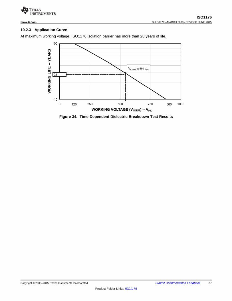
10.2.3 Application CurveAt maximum working voltage, ISO1176 isolation barrier has more than 28 years of life.
Figure 34. Time-Dependent Dielectric Breakdown Test Results
Copyright © 2008–2015, Texas Instruments Incorporated Submit Documentation Feedback 27
Product Folder Links: ISO1176

ISO1176SLLS897E –MARCH 2008–REVISED JUNE 2015 www.ti.com
11 Power Supply RecommendationsTo ensure reliable operation at all data rates and supply voltages, TI recommends a 0.1-μF bypass capacitor atinput and output supply pins (VCC1 and VCC2). The capacitors should be placed as close to the supply pins aspossible. If only a single primary-side power supply is available in an application, isolated power can begenerated for the secondary-side with the help of a transformer driver such as TI's SN6501. For suchapplications, detailed power supply design and transformer selection recommendations are available in SN6501data sheet (SLLSEA0).
12 Layout
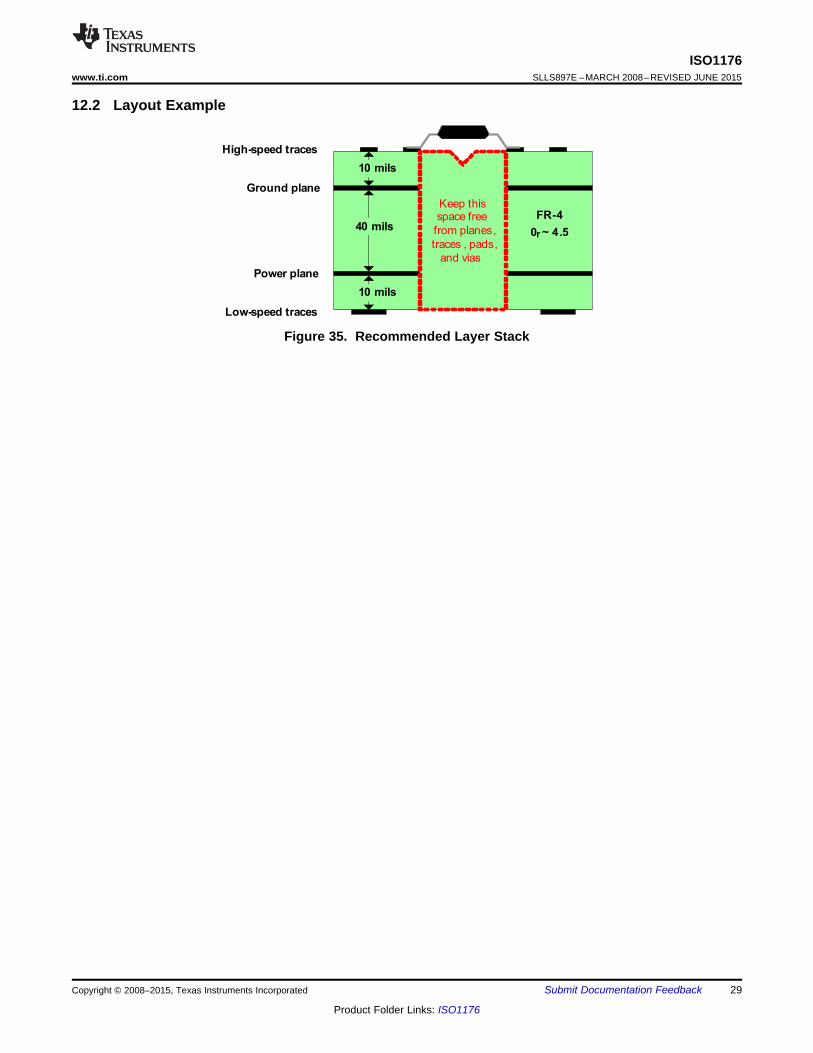
12.1 Layout GuidelinesON-chip IEC-ESD protection is good for laboratory and portable equipment but never sufficient for EFT andsurge transients occurring in industrial environments. Therefore, robust and reliable bus node design requires theuse of external transient protection devices. Because ESD and EFT transients have a wide frequency bandwidthfrom approximately 3-MHz to 3-GHz, high-frequency layout techniques must be applied during PCB design. Aminimum of four layers is required to accomplish a low EMI PCB design (see Figure 35).• Layer stacking should be in the following order (top-to-bottom): high-speed signal layer, ground plane, power
plane, and low-frequency signal layer.• Placing a solid ground plane next to the high-speed signal layer establishes controlled impedance for
transmission line interconnects and provides an excellent low-inductance path for the return current flow.• Placing the power plane next to the ground plane creates additional high-frequency bypass capacitance of
approximately 100 pF/in2.• Routing the slower speed control signals on the bottom layer allows for greater flexibility as these signal links
usually have margin to tolerate discontinuities such as vias.• Place the protection circuitry close to the bus connector to prevent noise transients from penetrating your
board.• Use VCC and ground planes to provide low-inductance. High-frequency currents might follow the path of least
inductance and not necessarily the path of least resistance.• Design the protection components into the direction of the signal path. Do not force the transient currents to
divert from the signal path to reach the protection device.• Apply 0.1-µF bypass capacitors as close as possible to the VCC-pins of transceiver, UART, and controller ICs
on the board.• Use at least two vias for VCC and ground connections of bypass capacitors and protection devices to
minimize effective via-inductance.• Use 1-kΩ to 10-kΩ pullup and pulldown resistors for enable lines to limit noise currents in theses lines during
transient events.• Insert pulse-proof resistors into the A and B bus lines if the TVS clamping voltage is higher than the specified
maximum voltage of the transceiver bus pins. These resistors limit the residual clamping current into thetransceiver and prevent it from latching up.
• While pure TVS protection is sufficient for surge transients up to 1 kV, higher transients require metal-oxidevaristors (MOVs) which reduce the transients to a few hundred volts of clamping voltage, and transientblocking units (TBUs) that limit transient current to less than 1 mA.
• Routing the high-speed traces on the top layer avoids the use of vias (and the introduction of theirinductances) and allows for clean interconnects between the isolator and the transmitter and receiver circuitsof the data link.
If an additional supply voltage plane or signal layer is needed, add a second power and ground plane system tothe stack to keep it symmetrical. This makes the stack mechanically stable and prevents it from warping. Also thepower and ground plane of each power system can be placed closer together, thus increasing the high-frequencybypass capacitance significantly.
NOTEFor detailed layout recommendations, see Application Note Digital Isolator Design Guide,SLLA284.
28 Submit Documentation Feedback Copyright © 2008–2015, Texas Instruments Incorporated
Product Folder Links: ISO1176
10 mils
10 mils
40 milsFR-4
0r ~ 4.5
Keep thisspace free
from planes,
traces , pads,
and vias
Ground plane
Power plane
Low-speed traces
High-speed traces
ISO1176www.ti.com SLLS897E –MARCH 2008–REVISED JUNE 2015
12.2 Layout Example
Figure 35. Recommended Layer Stack
Copyright © 2008–2015, Texas Instruments Incorporated Submit Documentation Feedback 29
Product Folder Links: ISO1176
ISO1176SLLS897E –MARCH 2008–REVISED JUNE 2015 www.ti.com
13 Device and Documentation Support
13.1 Documentation Support
13.1.1 Related DocumentationFor related documentation see the following:• SLLA284, Digital Isolator Design Guide• SLLSEA0, Transformer Driver for Isolated Power Supplies• SLLA353, Isolation Glossary
13.2 Community ResourcesThe following links connect to TI community resources. Linked contents are provided "AS IS" by the respectivecontributors. They do not constitute TI specifications and do not necessarily reflect TI's views; see TI's Terms ofUse.
TI E2E™ Online Community TI's Engineer-to-Engineer (E2E) Community. Created to foster collaborationamong engineers. At e2e.ti.com, you can ask questions, share knowledge, explore ideas and helpsolve problems with fellow engineers.
Design Support TI's Design Support Quickly find helpful E2E forums along with design support tools andcontact information for technical support.
13.3 TrademarksE2E is a trademark of Texas Instruments.All other trademarks are the property of their respective owners.
13.4 Electrostatic Discharge CautionThese devices have limited built-in ESD protection. The leads should be shorted together or the device placed in conductive foamduring storage or handling to prevent electrostatic damage to the MOS gates.
13.5 GlossarySLYZ022 — TI Glossary.
This glossary lists and explains terms, acronyms, and definitions.
14 Mechanical, Packaging, and Orderable InformationThe following pages include mechanical, packaging, and orderable information. This information is the mostcurrent data available for the designated devices. This data is subject to change without notice and revision ofthis document. For browser-based versions of this data sheet, refer to the left-hand navigation.
30 Submit Documentation Feedback Copyright © 2008–2015, Texas Instruments Incorporated
Product Folder Links: ISO1176
PACKAGE OPTION ADDENDUM
www.ti.com 11-Apr-2013
Addendum-Page 1
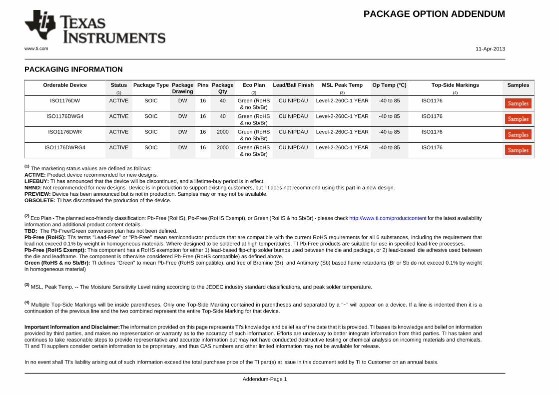
PACKAGING INFORMATION
Orderable Device Status(1)
Package Type PackageDrawing
Pins PackageQty
Eco Plan(2)
Lead/Ball Finish MSL Peak Temp(3)
Op Temp (°C) Top-Side Markings(4)
Samples
ISO1176DW ACTIVE SOIC DW 16 40 Green (RoHS& no Sb/Br)
CU NIPDAU Level-2-260C-1 YEAR -40 to 85 ISO1176
ISO1176DWG4 ACTIVE SOIC DW 16 40 Green (RoHS& no Sb/Br)
CU NIPDAU Level-2-260C-1 YEAR -40 to 85 ISO1176
ISO1176DWR ACTIVE SOIC DW 16 2000 Green (RoHS& no Sb/Br)
CU NIPDAU Level-2-260C-1 YEAR -40 to 85 ISO1176
ISO1176DWRG4 ACTIVE SOIC DW 16 2000 Green (RoHS& no Sb/Br)
CU NIPDAU Level-2-260C-1 YEAR -40 to 85 ISO1176
(1) The marketing status values are defined as follows:ACTIVE: Product device recommended for new designs.LIFEBUY: TI has announced that the device will be discontinued, and a lifetime-buy period is in effect.NRND: Not recommended for new designs. Device is in production to support existing customers, but TI does not recommend using this part in a new design.PREVIEW: Device has been announced but is not in production. Samples may or may not be available.OBSOLETE: TI has discontinued the production of the device.
(2) Eco Plan - The planned eco-friendly classification: Pb-Free (RoHS), Pb-Free (RoHS Exempt), or Green (RoHS & no Sb/Br) - please check http://www.ti.com/productcontent for the latest availabilityinformation and additional product content details.TBD: The Pb-Free/Green conversion plan has not been defined.Pb-Free (RoHS): TI's terms "Lead-Free" or "Pb-Free" mean semiconductor products that are compatible with the current RoHS requirements for all 6 substances, including the requirement thatlead not exceed 0.1% by weight in homogeneous materials. Where designed to be soldered at high temperatures, TI Pb-Free products are suitable for use in specified lead-free processes.Pb-Free (RoHS Exempt): This component has a RoHS exemption for either 1) lead-based flip-chip solder bumps used between the die and package, or 2) lead-based die adhesive used betweenthe die and leadframe. The component is otherwise considered Pb-Free (RoHS compatible) as defined above.Green (RoHS & no Sb/Br): TI defines "Green" to mean Pb-Free (RoHS compatible), and free of Bromine (Br) and Antimony (Sb) based flame retardants (Br or Sb do not exceed 0.1% by weightin homogeneous material)
(3) MSL, Peak Temp. -- The Moisture Sensitivity Level rating according to the JEDEC industry standard classifications, and peak solder temperature.
(4) Multiple Top-Side Markings will be inside parentheses. Only one Top-Side Marking contained in parentheses and separated by a "~" will appear on a device. If a line is indented then it is acontinuation of the previous line and the two combined represent the entire Top-Side Marking for that device.
Important Information and Disclaimer:The information provided on this page represents TI's knowledge and belief as of the date that it is provided. TI bases its knowledge and belief on informationprovided by third parties, and makes no representation or warranty as to the accuracy of such information. Efforts are underway to better integrate information from third parties. TI has taken andcontinues to take reasonable steps to provide representative and accurate information but may not have conducted destructive testing or chemical analysis on incoming materials and chemicals.TI and TI suppliers consider certain information to be proprietary, and thus CAS numbers and other limited information may not be available for release.
In no event shall TI's liability arising out of such information exceed the total purchase price of the TI part(s) at issue in this document sold by TI to Customer on an annual basis.
PACKAGE OPTION ADDENDUM
www.ti.com 11-Apr-2013
Addendum-Page 2
TAPE AND REEL INFORMATION
*All dimensions are nominal
Device PackageType
PackageDrawing
Pins SPQ ReelDiameter
(mm)
ReelWidth
W1 (mm)
A0(mm)
B0(mm)
K0(mm)
P1(mm)
W(mm)
Pin1Quadrant
ISO1176DWR SOIC DW 16 2000 330.0 16.4 10.75 10.7 2.7 12.0 16.0 Q1
PACKAGE MATERIALS INFORMATION
www.ti.com 16-Aug-2013
Pack Materials-Page 1
*All dimensions are nominal
Device Package Type Package Drawing Pins SPQ Length (mm) Width (mm) Height (mm)
ISO1176DWR SOIC DW 16 2000 367.0 367.0 38.0
PACKAGE MATERIALS INFORMATION
www.ti.com 16-Aug-2013
Pack Materials-Page 2
GENERIC PACKAGE VIEW
Images above are just a representation of the package family, actual package may vary.Refer to the product data sheet for package details.
DW 16 SOIC - 2.65 mm max heightSMALL OUTLINE INTEGRATED CIRCUIT
4040000-2/H

www.ti.com
PACKAGE OUTLINE
C
TYP10.639.97
2.65 MAX
14X 1.27
16X 0.510.31
2X8.89
TYP0.330.10
0 - 80.30.1
(1.4)
0.25GAGE PLANE
1.270.40
A
NOTE 3
10.510.1
BNOTE 4
7.67.4
4221009/B 07/2016
SOIC - 2.65 mm max heightDW0016BSOIC
NOTES: 1. All linear dimensions are in millimeters. Dimensions in parenthesis are for reference only. Dimensioning and tolerancing per ASME Y14.5M. 2. This drawing is subject to change without notice. 3. This dimension does not include mold flash, protrusions, or gate burrs. Mold flash, protrusions, or gate burrs shall not exceed 0.15 mm, per side. 4. This dimension does not include interlead flash. Interlead flash shall not exceed 0.25 mm, per side.5. Reference JEDEC registration MS-013.
1 16
0.25 C A B
98
PIN 1 IDAREA
SEATING PLANE
0.1 C
SEE DETAIL A
DETAIL ATYPICAL
SCALE 1.500

www.ti.com
EXAMPLE BOARD LAYOUT
(9.75)R0.05 TYP
0.07 MAXALL AROUND
0.07 MINALL AROUND
(9.3)
14X (1.27)
R0.05 TYP
16X (1.65)
16X (0.6)
14X (1.27)
16X (2)
16X (0.6)
4221009/B 07/2016
SOIC - 2.65 mm max heightDW0016BSOIC
SYMM
SYMM
SEEDETAILS
1
8 9
16
SYMM
HV / ISOLATION OPTION8.1 mm CLEARANCE/CREEPAGE
NOTES: (continued) 6. Publication IPC-7351 may have alternate designs. 7. Solder mask tolerances between and around signal pads can vary based on board fabrication site.
METAL SOLDER MASKOPENING
NON SOLDER MASKDEFINED
SOLDER MASK DETAILS
OPENINGSOLDER MASK METAL
SOLDER MASKDEFINED
LAND PATTERN EXAMPLESCALE:4X
SYMM
1
8 9
16
IPC-7351 NOMINAL7.3 mm CLEARANCE/CREEPAGE
SEEDETAILS

www.ti.com
EXAMPLE STENCIL DESIGN
R0.05 TYPR0.05 TYP
16X (1.65)
16X (0.6)
14X (1.27)
(9.75)
16X (2)
16X (0.6)
14X (1.27)
(9.3)
4221009/B 07/2016
SOIC - 2.65 mm max heightDW0016BSOIC
NOTES: (continued) 8. Laser cutting apertures with trapezoidal walls and rounded corners may offer better paste release. IPC-7525 may have alternate design recommendations. 9. Board assembly site may have different recommendations for stencil design.
SYMM
SYMM
1
8 9
16
HV / ISOLATION OPTION8.1 mm CLEARANCE/CREEPAGE
SOLDER PASTE EXAMPLEBASED ON 0.125 mm THICK STENCIL
SCALE:4X
SYMM
SYMM
1
8 9
16
IPC-7351 NOMINAL7.3 mm CLEARANCE/CREEPAGE

IMPORTANT NOTICE
Texas Instruments Incorporated (TI) reserves the right to make corrections, enhancements, improvements and other changes to itssemiconductor products and services per JESD46, latest issue, and to discontinue any product or service per JESD48, latest issue. Buyersshould obtain the latest relevant information before placing orders and should verify that such information is current and complete.TI’s published terms of sale for semiconductor products (http://www.ti.com/sc/docs/stdterms.htm) apply to the sale of packaged integratedcircuit products that TI has qualified and released to market. Additional terms may apply to the use or sale of other types of TI products andservices.Reproduction of significant portions of TI information in TI data sheets is permissible only if reproduction is without alteration and isaccompanied by all associated warranties, conditions, limitations, and notices. TI is not responsible or liable for such reproduceddocumentation. Information of third parties may be subject to additional restrictions. Resale of TI products or services with statementsdifferent from or beyond the parameters stated by TI for that product or service voids all express and any implied warranties for theassociated TI product or service and is an unfair and deceptive business practice. TI is not responsible or liable for any such statements.Buyers and others who are developing systems that incorporate TI products (collectively, “Designers”) understand and agree that Designersremain responsible for using their independent analysis, evaluation and judgment in designing their applications and that Designers havefull and exclusive responsibility to assure the safety of Designers' applications and compliance of their applications (and of all TI productsused in or for Designers’ applications) with all applicable regulations, laws and other applicable requirements. Designer represents that, withrespect to their applications, Designer has all the necessary expertise to create and implement safeguards that (1) anticipate dangerousconsequences of failures, (2) monitor failures and their consequences, and (3) lessen the likelihood of failures that might cause harm andtake appropriate actions. Designer agrees that prior to using or distributing any applications that include TI products, Designer willthoroughly test such applications and the functionality of such TI products as used in such applications.TI’s provision of technical, application or other design advice, quality characterization, reliability data or other services or information,including, but not limited to, reference designs and materials relating to evaluation modules, (collectively, “TI Resources”) are intended toassist designers who are developing applications that incorporate TI products; by downloading, accessing or using TI Resources in anyway, Designer (individually or, if Designer is acting on behalf of a company, Designer’s company) agrees to use any particular TI Resourcesolely for this purpose and subject to the terms of this Notice.TI’s provision of TI Resources does not expand or otherwise alter TI’s applicable published warranties or warranty disclaimers for TIproducts, and no additional obligations or liabilities arise from TI providing such TI Resources. TI reserves the right to make corrections,enhancements, improvements and other changes to its TI Resources. TI has not conducted any testing other than that specificallydescribed in the published documentation for a particular TI Resource.Designer is authorized to use, copy and modify any individual TI Resource only in connection with the development of applications thatinclude the TI product(s) identified in such TI Resource. NO OTHER LICENSE, EXPRESS OR IMPLIED, BY ESTOPPEL OR OTHERWISETO ANY OTHER TI INTELLECTUAL PROPERTY RIGHT, AND NO LICENSE TO ANY TECHNOLOGY OR INTELLECTUAL PROPERTYRIGHT OF TI OR ANY THIRD PARTY IS GRANTED HEREIN, including but not limited to any patent right, copyright, mask work right, orother intellectual property right relating to any combination, machine, or process in which TI products or services are used. Informationregarding or referencing third-party products or services does not constitute a license to use such products or services, or a warranty orendorsement thereof. Use of TI Resources may require a license from a third party under the patents or other intellectual property of thethird party, or a license from TI under the patents or other intellectual property of TI.TI RESOURCES ARE PROVIDED “AS IS” AND WITH ALL FAULTS. TI DISCLAIMS ALL OTHER WARRANTIES ORREPRESENTATIONS, EXPRESS OR IMPLIED, REGARDING RESOURCES OR USE THEREOF, INCLUDING BUT NOT LIMITED TOACCURACY OR COMPLETENESS, TITLE, ANY EPIDEMIC FAILURE WARRANTY AND ANY IMPLIED WARRANTIES OFMERCHANTABILITY, FITNESS FOR A PARTICULAR PURPOSE, AND NON-INFRINGEMENT OF ANY THIRD PARTY INTELLECTUALPROPERTY RIGHTS. TI SHALL NOT BE LIABLE FOR AND SHALL NOT DEFEND OR INDEMNIFY DESIGNER AGAINST ANY CLAIM,INCLUDING BUT NOT LIMITED TO ANY INFRINGEMENT CLAIM THAT RELATES TO OR IS BASED ON ANY COMBINATION OFPRODUCTS EVEN IF DESCRIBED IN TI RESOURCES OR OTHERWISE. IN NO EVENT SHALL TI BE LIABLE FOR ANY ACTUAL,DIRECT, SPECIAL, COLLATERAL, INDIRECT, PUNITIVE, INCIDENTAL, CONSEQUENTIAL OR EXEMPLARY DAMAGES INCONNECTION WITH OR ARISING OUT OF TI RESOURCES OR USE THEREOF, AND REGARDLESS OF WHETHER TI HAS BEENADVISED OF THE POSSIBILITY OF SUCH DAMAGES.Unless TI has explicitly designated an individual product as meeting the requirements of a particular industry standard (e.g., ISO/TS 16949and ISO 26262), TI is not responsible for any failure to meet such industry standard requirements.Where TI specifically promotes products as facilitating functional safety or as compliant with industry functional safety standards, suchproducts are intended to help enable customers to design and create their own applications that meet applicable functional safety standardsand requirements. Using products in an application does not by itself establish any safety features in the application. Designers mustensure compliance with safety-related requirements and standards applicable to their applications. Designer may not use any TI products inlife-critical medical equipment unless authorized officers of the parties have executed a special contract specifically governing such use.Life-critical medical equipment is medical equipment where failure of such equipment would cause serious bodily injury or death (e.g., lifesupport, pacemakers, defibrillators, heart pumps, neurostimulators, and implantables). Such equipment includes, without limitation, allmedical devices identified by the U.S. Food and Drug Administration as Class III devices and equivalent classifications outside the U.S.TI may expressly designate certain products as completing a particular qualification (e.g., Q100, Military Grade, or Enhanced Product).Designers agree that it has the necessary expertise to select the product with the appropriate qualification designation for their applicationsand that proper product selection is at Designers’ own risk. Designers are solely responsible for compliance with all legal and regulatoryrequirements in connection with such selection.Designer will fully indemnify TI and its representatives against any damages, costs, losses, and/or liabilities arising out of Designer’s non-compliance with the terms and provisions of this Notice.
Mailing Address: Texas Instruments, Post Office Box 655303, Dallas, Texas 75265Copyright © 2017, Texas Instruments Incorporated
Recommended