Interdigitated
Back-contacted(IBC)
c-Si solar cells based on
laser processed dielectric layers
Thesis submitted in partial fulfillment of the requirement for the PhD Degree
issued by the Universitat Politectnica de Catalunya (UPC), in its Electronic
Engineering Program
Gema López Rodríguez
Co-directors: Dr. Pablo Rafael Ortega Villasclaras
Dr. Isidro Martín García
October 2016
Electronic Engineering Department
Agradecimientos
En primer lugar quiero agradecer a mis directores de tesis, los profesores Pablo
Ortega e Isidro Martín la dirección y supervisión de este trabajo de tesis. "Gracias
a los dos por resolver mis infinitas dudas, por toda vuestra ayuda, dedicación y
apoyo. -Gracias Pablo por esa energía infinita".
Gracias a Ramón Alcubilla, a Cristobal Voz y a Michael Vetter por haber
confiado en mi y haberme brindado la primera oportunidad de trabajar con el
grupo. Gracias también por todo vuestro apoyo a lo largo de estos años.
A los técnicos de la Sala Blanca Miguel y Xavi. Quiero agradecer muy es-
pecialmente, tanto a nivel profesional como personal a Miguel García. A nivel
profesional porque considero que es incuestionable el excelente trabajo que realiza
en la sala blanca, por toda su ayuda técnica, profesional y por todo lo aprendido
de él y a nivel personal por su amistad y por todos los buenos momentos "-Gracias
Miguel".
A David Muñoz y Carlos Molpecedes del Centro Laser de la UPM. Su ines-
timable coraboración ha sido clave para conseguir el 20% de eficiencia.
A Trifon Trifonov del Centre de Recerca en Nanoenginyeria CRne, por su
gran trabajo con el FIB/SEM y su tiempo para obtener siempre la mejor imagen
posible.
A Luis Enrique Romero y a Javier Pérez del Instituto de Ciencies Fotóniques,
ICFO, por horas y horas de ALD en las que siempre han estado disponibles para
solventar cualquier duda y problema.
Quisiera agradecer a los doctorandos del pasado y del presente, todos los
buenos momentos dentro y fuera de la universidad. Gracias por haber hecho y
hacer más agradable los días de trabajo: David Molinero, Gerard Villar, Jordi,
Rafa, Lukasz, Denis, Moises, Delfina, Kike, Enrique, Maziar, Vito, Carmina,
Martín, Gerard Masmitja, Rasha, Guillermo, Chen y Chenna.
A Santi Pérez (por ayudar siempre), Arnau, Teresa, Eric y Sergi por la in-
III
IV Agradecimientos
finidad de horas compartidas "working and post-working".
Finalmente y ya fuera del ámbito de la universidad quiero expresar mi sincera
gratitud a Kiko Rodriguez, Mónica DelaPirriera, Mónica Colina, Anna Belen,
David Hernandez y Juan Carlos por todos estos años de amistad. Y por último
gracias a mi familia por su apoyo incondicional, a mis padres, mis herman@s (JL,
JM y MA), cuñad@s y a mi sobrino Pablo.
This work has been supported by the MINECO under project TEC 2014-
59736-R and ENE2013-48629-C4-1-R and by the European UnionÂťs Seventh
Framework Programme for research, technological development and demonstra-
tion under project HERCULES (Grant agreement: 608498).
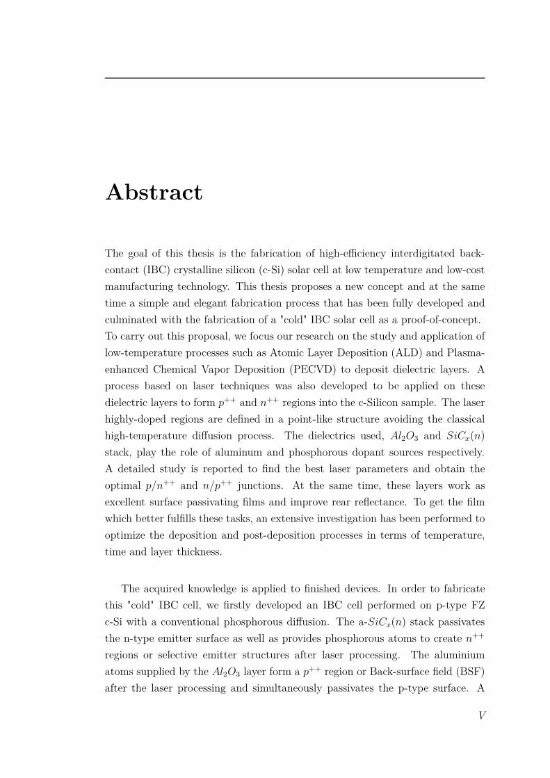
Abstract
The goal of this thesis is the fabrication of high-efficiency interdigitated back-
contact (IBC) crystalline silicon (c-Si) solar cell at low temperature and low-cost
manufacturing technology. This thesis proposes a new concept and at the same
time a simple and elegant fabrication process that has been fully developed and
culminated with the fabrication of a "cold" IBC solar cell as a proof-of-concept.
To carry out this proposal, we focus our research on the study and application of
low-temperature processes such as Atomic Layer Deposition (ALD) and Plasma-
enhanced Chemical Vapor Deposition (PECVD) to deposit dielectric layers. A
process based on laser techniques was also developed to be applied on these
dielectric layers to form p++ and n++ regions into the c-Silicon sample. The laser
highly-doped regions are defined in a point-like structure avoiding the classical
high-temperature diffusion process. The dielectrics used, Al2O3 and SiCx(n)
stack, play the role of aluminum and phosphorous dopant sources respectively.
A detailed study is reported to find the best laser parameters and obtain the
optimal p/n++ and n/p++ junctions. At the same time, these layers work as
excellent surface passivating films and improve rear reflectance. To get the film
which better fulfills these tasks, an extensive investigation has been performed to
optimize the deposition and post-deposition processes in terms of temperature,
time and layer thickness.
The acquired knowledge is applied to finished devices. In order to fabricate
this "cold" IBC cell, we firstly developed an IBC cell performed on p-type FZ
c-Si with a conventional phosphorous diffusion. The a-SiCx(n) stack passivates
the n-type emitter surface as well as provides phosphorous atoms to create n++
regions or selective emitter structures after laser processing. The aluminium
atoms supplied by the Al2O3 layer form a p++ region or Back-surface field (BSF)
after the laser processing and simultaneously passivates the p-type surface. A
V

VI Abstract
promising efficiency of 18.7% (Jsc = 39.1 mA/cm2, Voc = 638 mV, FF = 75.3%)
was obtained as a result of this new concept.
The first "cold" IBC cell was obtained on n-type substrate. The conventional
phosphorous diffusion is eliminated and the fabrication steps are rearranged in
order to reduce the thermal budget and the complex photolithographic steps.
The laser employed was a pulsed Nd-YAG lamp-pumped working at 1064 nm in
the nanosecond regime. The efficiency achieved was 18.0% (Jsc = 39.2 mA/cm2,
Voc = 647 mV, FF = 71.1%) on 280 µm thick 2.5± 0.5 Ωcm n-type FZ c-Si with
a designated area of 9 cm2. Finally, the efficiency achieved of the "Cold" IBC
cell was boosted to 20% (Jsc = 40.5 mA/cm2, Voc = 650 mV and FF= 76.4%),
changing the employed laser by a pulsed Nd:YVO4 laser operating at 355 nm
(UV) with a better laser power control and improving the FF by decreasing de
pitch from 250 µm to 125 µm.
Contents
I
Agradecimientos III
Abstract V
1 Introduction 1
1.1 Market Overview . . . . . . . . . . . . . . . . . . . . . . . . . . . 1
1.2 Thesis motivation . . . . . . . . . . . . . . . . . . . . . . . . . . . 6
1.3 Thesis Outline . . . . . . . . . . . . . . . . . . . . . . . . . . . . . 8
2 Fundamental Background 17
2.1 Fundamental parameters of solar cells . . . . . . . . . . . . . . . . 17
2.1.1 Introduction . . . . . . . . . . . . . . . . . . . . . . . . . . 17
2.1.2 p-n junction . . . . . . . . . . . . . . . . . . . . . . . . . . 18
2.1.3 The solar cell . . . . . . . . . . . . . . . . . . . . . . . . . 19
2.1.4 Intrinsic losses limitations . . . . . . . . . . . . . . . . . . 22
2.2 Review of back-contact silicon solar cells . . . . . . . . . . . . . . 23
2.2.1 Metallization and Emitter Wrap Through (MWT and EWT)
solar cells . . . . . . . . . . . . . . . . . . . . . . . . . . . 25
2.2.2 Back-contact back-junction (BC-BJ) solar cells . . . . . . . 27
2.2.3 Technological challenges of BC-BJ solar cells . . . . . . . . 28
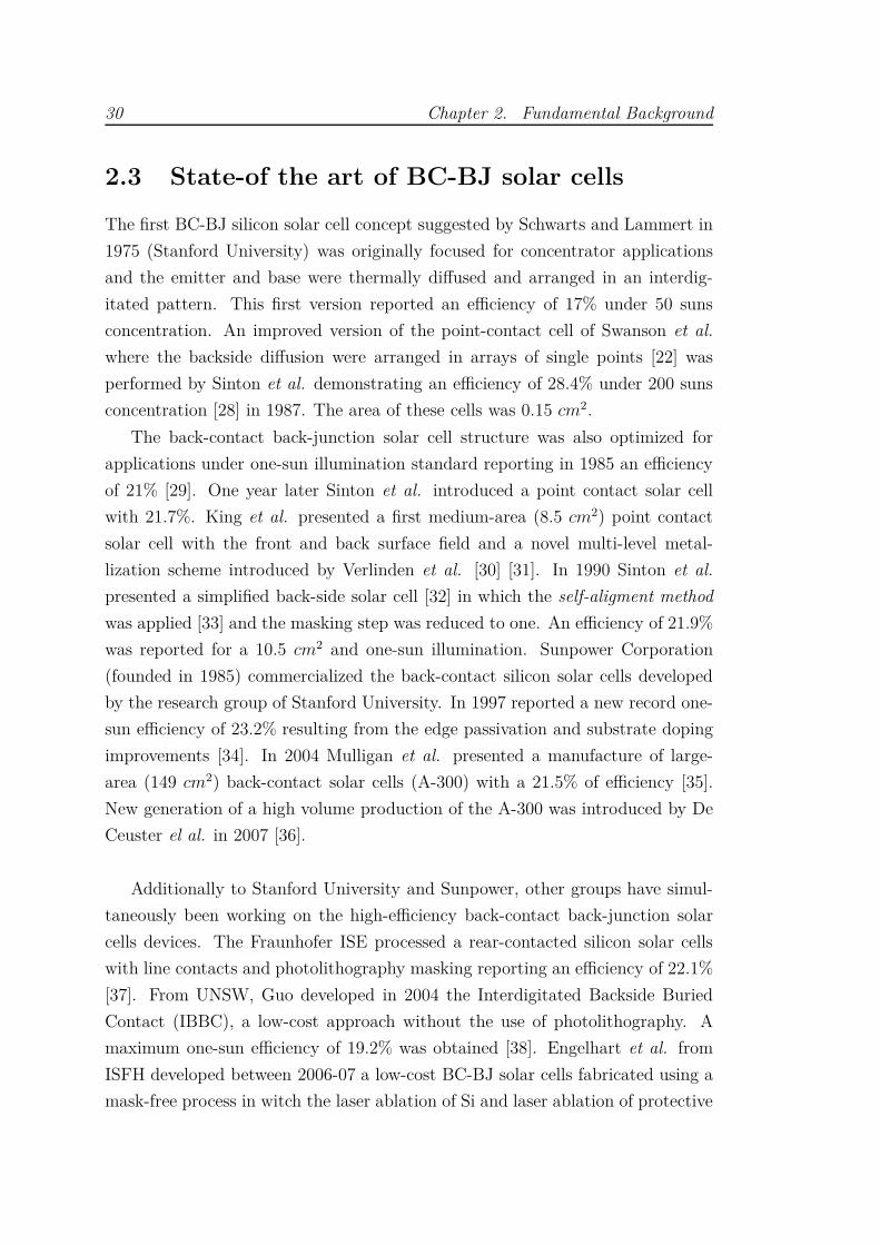
2.3 State-of the art of BC-BJ solar cells . . . . . . . . . . . . . . . . . 30
2.4 Experimental techniques . . . . . . . . . . . . . . . . . . . . . . . 34
2.4.1 Cleaning and wet texturing . . . . . . . . . . . . . . . . . 34
2.4.2 Thermal Atomic Layer Deposition, ALD . . . . . . . . . . 38
2.4.3 Plasma Enhanced Chemical Vapour Deposition,
PECVD . . . . . . . . . . . . . . . . . . . . . . . . . . . . 39
VII

VIII Contents
2.4.4 Laser . . . . . . . . . . . . . . . . . . . . . . . . . . . . . . 41
2.4.5 Characterization systems . . . . . . . . . . . . . . . . . . . 41
3 c-Si surface passivation by Al2O3 thin films 53
3.1 Introduction . . . . . . . . . . . . . . . . . . . . . . . . . . . . . . 53
3.2 Recombination in the bulk of c-Si . . . . . . . . . . . . . . . . . . 54
3.2.1 Radiative recombination . . . . . . . . . . . . . . . . . . . 55
3.2.2 Auger recombination . . . . . . . . . . . . . . . . . . . . . 56
3.2.3 Recombination through defects in the bandgap, SRH . . . 58
3.3 Recombination at c-Si surface . . . . . . . . . . . . . . . . . . . . 61
3.4 The Effective lifetime of c-Si . . . . . . . . . . . . . . . . . . . . . 63
3.5 State-of-the-art of c-Si surface passivation . . . . . . . . . . . . . 64
3.5.1 Thermally grown silicon dioxide, SiO2 . . . . . . . . . . . 65
3.5.2 Amorphous silicon-based compounds . . . . . . . . . . . . 66
3.5.3 Aluminum oxide, Al2O3 . . . . . . . . . . . . . . . . . . . 68
3.6 c-Si surface passivation by Al2O3 thin films . . . . . . . . . . . . . 69
3.6.1 Introduction . . . . . . . . . . . . . . . . . . . . . . . . . . 69
3.6.2 Influence of the ALD deposition temperature and anneal-
ing treatment (time and temperature) on surface recombi-
nation velocity . . . . . . . . . . . . . . . . . . . . . . . . 70
3.6.3 Influence of Al2O3 thickness on surface recombination velocity 72
3.6.4 Al2O3/a − SiCx surface passivating stacks.
Experimental . . . . . . . . . . . . . . . . . . . . . . . . . 75
3.6.5 Al2O3/a − SiCx stacks. Optical characterization. . . . . . 78
3.7 CONCLUSION . . . . . . . . . . . . . . . . . . . . . . . . . . . . 82
4 Emitter formation using laser doping technique on n- and p-type
c-Si substrates 91
4.1 Introduction . . . . . . . . . . . . . . . . . . . . . . . . . . . . . . 91
4.2 Experimental . . . . . . . . . . . . . . . . . . . . . . . . . . . . . 92
4.2.1 Laser system . . . . . . . . . . . . . . . . . . . . . . . . . 92
4.2.2 Sample preparation . . . . . . . . . . . . . . . . . . . . . . 93
4.3 Experimental results. J-V measurements . . . . . . . . . . . . . . 95
4.3.1 Hydrofluoric acid treatment. . . . . . . . . . . . . . . . . . 97
4.4 Conclusion . . . . . . . . . . . . . . . . . . . . . . . . . . . . . . . 101

Contents IX
5 The "Hybrid" IBC solar cell 105
5.1 Introduction . . . . . . . . . . . . . . . . . . . . . . . . . . . . . . 105
5.2 Precursor samples. Diodes . . . . . . . . . . . . . . . . . . . . . . 106
5.3 Emitter saturation current (Joe) study . . . . . . . . . . . . . . . 108
5.4 "Hybrid" IBC Fabrication process . . . . . . . . . . . . . . . . . . 110
5.5 J-V measurements and Suns-Voc . . . . . . . . . . . . . . . . . . . 116
5.6 Optical losses analysis and Quantum
Efficiency of the "Hybrid" IBC cells . . . . . . . . . . . . . . . . . 119
5.6.1 Simulation of the solar cell optics . . . . . . . . . . . . . . 120
5.6.2 External quantum efficiency analysis . . . . . . . . . . . . 123
5.7 Conclusion . . . . . . . . . . . . . . . . . . . . . . . . . . . . . . . 127
6 "Cold" Back-contact Back-junction silicon solar cells 131
6.1 Introduction . . . . . . . . . . . . . . . . . . . . . . . . . . . . . . 131
6.2 Surface passivation and minority diffusion length . . . . . . . . . 133
6.3 Sheet resistance . . . . . . . . . . . . . . . . . . . . . . . . . . . . 134
6.4 Precursor samples. Diodes . . . . . . . . . . . . . . . . . . . . . . 135
6.4.1 p++ region . . . . . . . . . . . . . . . . . . . . . . . . . . . 135
6.4.2 n++ region . . . . . . . . . . . . . . . . . . . . . . . . . . . 137
6.5 Emitter saturation current (Joe) . . . . . . . . . . . . . . . . . . . 139
6.6 "Cold" IBC structure and fabrication process. . . . . . . . . . . . 141
6.7 J-V measurements and Suns-Voc . . . . . . . . . . . . . . . . . . . 147
6.8 Optical losses analysis and Quantum
Efficiency of the "Cold" IBC cells . . . . . . . . . . . . . . . . . . 150
6.8.1 Simulation of the solar cell optics . . . . . . . . . . . . . . 151
6.8.2 External quantum efficiency analysis . . . . . . . . . . . . 154
6.9 "Cold" IBC fabrication using 400 ns of pulse duration for emitter
and BSF formation . . . . . . . . . . . . . . . . . . . . . . . . . . 156
6.9.1 "Cold" IBC surface passivation . . . . . . . . . . . . . . . . 157
6.9.2 Precursor samples. Diodes p++/n . . . . . . . . . . . . . . 157
6.9.3 Emitter saturation current (Joe) . . . . . . . . . . . . . . . 158
6.9.4 J-V measurements, Suns-Voc and EQE . . . . . . . . . . . 159
6.10 Conclusion . . . . . . . . . . . . . . . . . . . . . . . . . . . . . . . 166
7 One step forward!. Achieving high-efficiency solar cell 169
7.1 Optimization of laser-doped contacts . . . . . . . . . . . . . . . . 170

X Contents
7.1.1 Laser system . . . . . . . . . . . . . . . . . . . . . . . . . 170
7.1.2 Sheet resistance (Rsheet) and precursor diodes . . . . . . . 170
7.2 "Cold" IBC solar cells characterization . . . . . . . . . . . . . . . 175
7.2.1 J-V measurements and Suns-Voc . . . . . . . . . . . . . . . 176
7.3 Conclusions . . . . . . . . . . . . . . . . . . . . . . . . . . . . . . 180
8 Summary and Future Work 183
8.1 Summary . . . . . . . . . . . . . . . . . . . . . . . . . . . . . . . 183
8.2 Future works . . . . . . . . . . . . . . . . . . . . . . . . . . . . . 186
8.3 List of publications . . . . . . . . . . . . . . . . . . . . . . . . . . 187
8.3.1 Refereed journal paper . . . . . . . . . . . . . . . . . . . . 187
8.3.2 Other related publications . . . . . . . . . . . . . . . . . . 187
8.3.3 National and International conferences . . . . . . . . . . . 188
Chapter 1
Introduction
Solar cells transform sunlight directly into electricity and they are a promising
technology for satisfying the current and future energy demands in a sustainable
and environmentally friendly way.
1.1 Market Overview
Fossil fuels such a coal, oil and natural gas are and will be in a short term the most
used form of energy. However, their relative share in the future energy supply will
be significantly decreased. The limited reserves of the fossil fuels as well as cli-
mate change caused by the emission of greenhouse gases are the major problems
that directly concern the humanity as a cause and effect. Therefore, the transi-
tion from fossil energy sources to a clean and renewable energy (wind, biomass,
water and solar) is a clear alternative and challenge for the present and the future.
The Earth receives incoming solar radiation from the sun in just one hour to
cover the present global annual energy consumption. Solar energy is an abundant
and widely available source of energy that can be directly converted into electricity
by the photovoltaic cells without any emissions.
Since the first commercial use of solar cells in the late 1950’s for powering
satellites, the market of solar cells has followed a rapid expansion with a variety
of end uses including grid connected systems, consumer products and remote area
power supply. The PV market has remarkably progressed and has maintained a
continuous growth in the past decade, even during difficult economic times. As it
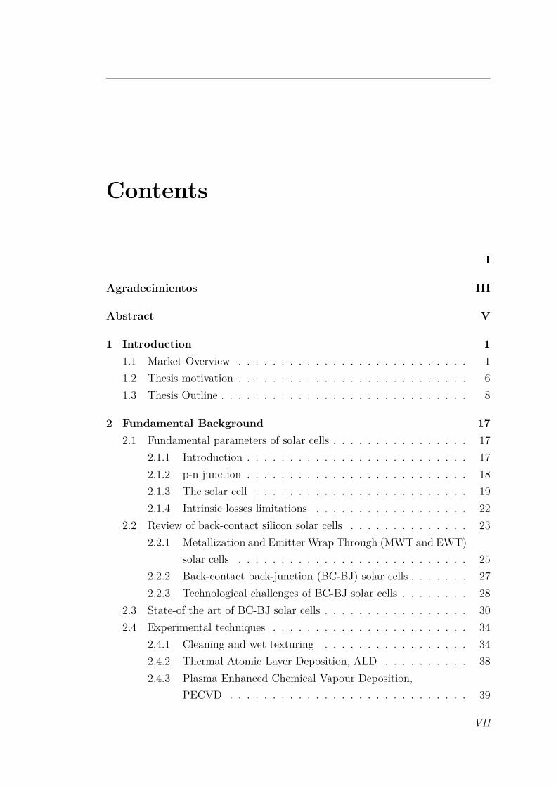
is shown in Fig. 1.1, at the end of 2009, the world’s cumulative installed capacity
1
2 Chapter 1. Introduction
was more than 23 GW. One year later it was 40.3 GW and by the end of 2014,
cumulative photovoltaic capacity reached at least 178 GW, sufficient to supply 1
percent of global electricity demands1 [1].
0
50000
100000
150000
200000
20
06
20
07
20
08
20
09
20
10
20
11
20
12
20
13
20
14
MW
p
Rest of the World
China
Asia-Pacific
Middle East and
Africa
Americas
Europe
Figure 12
Figure 1.1: Evolution of global PV cumulative installed capacity 2006-2014.Data extrated from The European Photovoltaic Industry Association (EPIA)
However and for the first time in more than a decade, the Europe market lost
its leadership to Asia in terms of new installations (China was the top market
in 2013 with 11.8GW, Japan with 6.9 GW in front of 3.3 GW from Germany,
the top European market) and these non-European markets (among others i.e.
USA) are keeping the global PV development on, compensating the European
slowdown as a consequence of political decisions to reduce PV incentives and the
financial situation [1] (Fig. 1.2).
Figure 1.3 shows the cumulative capacity forecasts for global PV by 2020.
Conservative scenario capacity foresee to reach 400GW, assuming declining an-
nual installations from current levels, while more optimistic scenarios project
cumulative capacity to grow beyond 500 GW [2].
1During the closing months of 2015, the global PV industry grown a 35 percent, global PVinstallations are forecast to grow an additional 17 percent in 2016, culminating in 21 GW ofPV to be installed worldwide in the fourth quarter

1.1. Market Overview 3
Germany
20%
Italy
10%
ROW
9% Rest of Europe
18%
North America
12%
Japan
13%
China&Taiwan
18%
Global Cumulative PV Installation by Region
Figure 1.2: The total cumulative installations amounted to 178 GWp at the end 2014.Allpercentages are related to total global installations, including off-grid systems.
0
100000
200000
300000
400000
500000
600000
20
06
20
08
20
10
20
12
20
14
20
16
20
18
MW
p
High scenario
Low scenario
Average projection
Historical cumulative
capacity
Figure 1.3: Projected global cumulative capacity. Source: EPIA

4 Chapter 1. Introduction
The International Energy Agency proposed in its latest edition of the Tech-
nology Roadmap: Solar Photovoltaic Energy report, a revised long-term scenario
for 2050 that would occur if underlying economic, regulatory and political con-
ditions played out. Figure 1.4 envisages up to 16% of global electricity for solar
PV with 6300 TWh generated in 2050. In order to achieve IEA’s projection, PV
deployment of 124 GW and investments of $225 billion are required annually.
7000
6000
3000
5000
4000
2000
1000
0 2025 2015 2030 2020 2045 2035 2040 2050
PV
ele
ctri
city
ge
ne
rati
on
(T
Wh
)
10%
8%
0%
2%
4%
6%
14%
12%
16%
18%
Sh
are
of
tota
l e
lect
rici
ty g
en
era
tio
n
United States
Middle East Other developing Asia Eastern Europe and FSU
Other OECD Americas European Union Other OECD China India Africa
Non-OECD Americas Share of total Scenario
Figure 1.4: Regional production of PV electricity envisioned in the IEA’s roapmad [3]
In Europe, photovoltaic energy covers 3.5% of energy demand and 6% of the
peak electricity demand [3] and in it could cover between 10% and 15% in 2030
if the political scenario is favourable. However, without major changes of policy,
PV contribution to the final electricity demand, could be by 2030, between 7%
and 11%. In a short-term prospects for the European markets are stable in the
best case, and could even decline. In the worst scenario, without support from
policymakers for PV, the transition to a cost-competitive PV market driven less
by financial support schemes could be difficult over the five years to come.
Economies of scale, technological improvements and intense competition which
lead to module oversupply have been also responsible for achieving continued cost
reductions. The average price per watt has dropped drastically for solar cells over
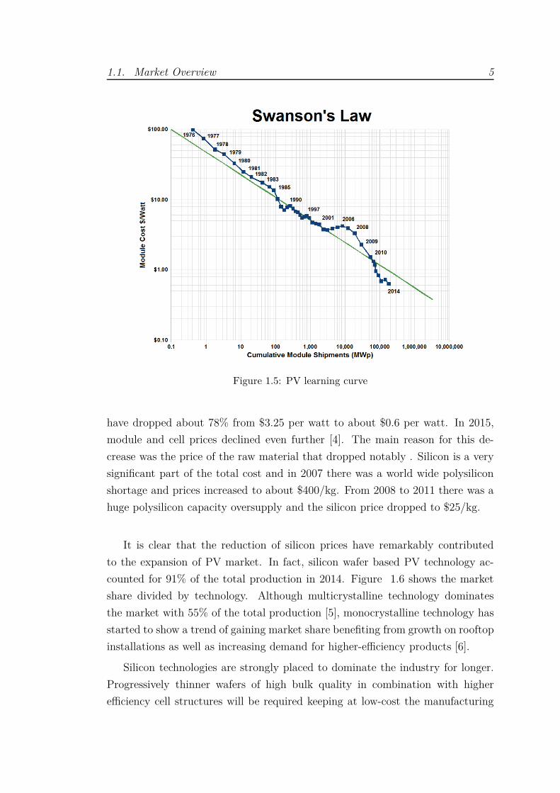
the last few decades following the named Swanson’s Law (Fig. 1.5) which states
that the per-watt cost of solar cells and panels fall by 20% for every doubling of
cumulative photovoltaic production.
As it can be seen from the graph, recent solar module prices have experienced
a dramatic price reduction. From 2006 to 2014 worldwide average module prices
1.1. Market Overview 5
Figure 1.5: PV learning curve
have dropped about 78% from $3.25 per watt to about $0.6 per watt. In 2015,
module and cell prices declined even further [4]. The main reason for this de-
crease was the price of the raw material that dropped notably . Silicon is a very
significant part of the total cost and in 2007 there was a world wide polysilicon
shortage and prices increased to about $400/kg. From 2008 to 2011 there was a
huge polysilicon capacity oversupply and the silicon price dropped to $25/kg.
It is clear that the reduction of silicon prices have remarkably contributed
to the expansion of PV market. In fact, silicon wafer based PV technology ac-
counted for 91% of the total production in 2014. Figure 1.6 shows the market
share divided by technology. Although multicrystalline technology dominates
the market with 55% of the total production [5], monocrystalline technology has
started to show a trend of gaining market share benefiting from growth on rooftop
installations as well as increasing demand for higher-efficiency products [6].
Silicon technologies are strongly placed to dominate the industry for longer.
Progressively thinner wafers of high bulk quality in combination with higher
efficiency cell structures will be required keeping at low-cost the manufacturing

6 Chapter 1. Introduction
Multi-Si
55%
Thin Film
9%
CIGS 3.4%
a-Si 1.6%
CdTe 4%
Mono-Si
36%
Global Market Share by Technology
Figure 1.6: Global PV market by technology in 2014. Source: "Photovoltaics Report".Fraunhofer ISE. August 2015
technology.
1.2 Thesis motivation
From the above overview, the short and medium term for industrial solar cells
appears to be based on mono and multicrystalline silicon wafers. The substrates
will be progressively thinner for costs reasons and surface recombination losses
thus become more significant and even dominant for high quality substrates. The
minimization of surface recombination losses, known as surface passivation is then
crucial to achieve high-efficiency solar cells.
An emerging technology that offers high quality passivation at low temperature
is Atomic Layer deposited, (ALD) aluminum oxide (Al2O3) films. The main
advantages that ALD technique offers are:
• Ultimate control of film growth and thickness (mono-layer growth control)
• Extremely high conformality/step coverage (very good coverage of textured
surfaces
• Good uniformity on large substrates (easily scalable up to > 300mm wafers)

1.2. Thesis motivation 7
• Relatively low substrates temperatures, typically 200-400°C (even RT)
For the PV industry, high-throughput spatial and batch ALD equipment have
been designed in the last few years and are already commercially available [7].
The study of the passivation quality of Al2O3 deposited by thermal ALD for a va-
riety of different surface conditions is an important topic in this thesis and is the
continuation of previous work developed in a master-thesis work. Furthermore,
the optical properties makes Al2O3 ideal for photovoltaic applications as a single
layer anti-reflection coating. Therefore, Al2O3 films deposited by ALD technique
offer great potential for increasing the efficiency of industrial crystalline silicon
solar cells without increasing the fabrication cost.
On the other hand, conventional high-temperature thermal diffusion to cre-
ate n+ and p+ regions in c-Si solar cells represents one of the most expensive
and time-consuming processes in the solar cell fabrication line. Laser appears as
a good candidate to achieve highly doped regions at low temperature and low
manufacturing cost. Lasers are widely used for different applications in the in-
dustry of solar cells such as scribing grooves in buried contact solar cells [8], firing
contacts in the laser fired contact (LFC) structure[9],[10], [11],texturing surfaces
[12],[13], ablating dielectrics layers [14], among others. Several methods apply-
ing laser doping technique (LD) to junction formation have been presented to
date and a wide variety of dopant source can be used in gas, liquid or solid form
[15],[16],[17],[18].
In the last years our research group (Micro and Nanotechnologies, MNT) at the
UPC has developed and optimized a laser process on phosphorus-doped silicon
carbide stack a-SiCx(n) for the creation of n+ region and successfully applied
to the rear contact of heterojunction solar cell [19],[20],[21]. Previous group
knowledge has been used as starting point and during this thesis laser doped
technique has been optimized to create highly-doped regions into c-Si using a-
SiCx(n) stack deposited by PECVD and Al2O3 by thermal ALD and consequently
reducing the global thermal budget of the solar cell fabrication. The main ad-
vantage of these dielectric layers is that, if they are correctly tuned, they can
work as c-Si surface passivating layers, dopant source and reduce the optical re-
flectance simultaneously. Results of this study have been published in several
papers [22],[11],[18],[23],[24],[25].
8 Chapter 1. Introduction
The highest conversion efficiency of crystalline solar cell for one-sun applica-
tions is 26.3% and was achieved in a practical size (180 cm2) by Kaneka Cor-
poration in September 2016. This recent new record was based on Back-contact
back-junction structure with heterojunction technology. This achievement breaks
the past world record of 25.6% by ∼ 0.7 %, achieved by Panasonic (2014) using
the same heterojunction back-contact type structure [26].
MNT research group has acquired in the last years an extensive experience
on interdigitated back-contact solar cells fabrication [27] and together with Aalto
University have achieved the world record in Black Silicon solar cells with interdi-
gitated back-contacts (IBC) [28]. However this cell structure is quite complex and
its fabrication involves multiple masking steps, high temperature diffusion and
extremely well aligned processes. Due to the potential of high-efficiency devices
combined with low-cost fabrication process, the last part of this thesis consists
of applying dielectric layers previously studied to fabricate the final IBC solar
cell. High surface passivation quality and good antireflection properties in the
photovoltaic range are needed. On the other hand, these layers have to provide
enough quantity of dopant to originate p+ and n+ regions into c-Si either to form
a Back-surface field or np+/pn+ junction. Thus, optimized laser conditions, i.e.
laser power, mode and number of pulses are required. Combining these dielectric
layers with laser processing has the potential to drastically simplify the fabrication
of IBC c-Si solar cells.
1.3 Thesis Outline
This thesis work has one main and a clear objective: the fabrication of a "cold"
IBC, i.e. An interdigitated back-contact solar cell that do not involve the conven-
tional high-temperature diffusion neither time-consuming and complex processes.
In order to achieve this final objective, the followed methodology can be seen in
figure 1.7 together with the corresponding chapters of the thesis.

1.3. Thesis Outline 9
Optical
characterization
Precursor diodes.
Laser parameter
characterization
Surface passivation
“Hybrid” IBC
fabrication
“Cold” IBC
fabrication
Chapter 3 Chapter 4
Chapter 5
Chapter 6,7
Figure 1.7: Schematic of the experimental flow developed along this thesis work.

10 Chapter 1. Introduction
High vacuum gate
Turbo molecular pumps
Process chamber Load lock chamber
Sample
Plasma
Heater
Electrode
Gas flow
Chapter 2 is the starting point of this thesis.
Fundamental background as basic concepts and
parameters of crystalline silicon solar cells as well
as the intrinsic limitations are presented. Back-
contacted silicon solar cell designs are briefly in-
troduced and special attention is paid to IBC
structure and a short historic overview is given.
The last part of this chapter comprises the ex-
planation of the fundamental equipment used in this thesis for processing and
characterization.
Sef
f,m
ax
T
In Chapter 3 basic concepts of recom-
bination mechanisms and surface passivating
films in c-Si are presented. Next, we study
in detail the Al2O3 layer and Al2O3/a −
SiCx stacks as passivating films. Surface
recombination velocity has been analyzed as
a function of deposition temperature, annea-
ling time and temperature and thickness
film.
Ref
lect
an
ce (
%)
As a second step optical properties of the
studied films i.e. Al2O3 and Al2O3/a − SiCx
stack are also analyzed in this chapter. Re-
flectance properties on polish and textured c-Si
are evaluated in order to find the best film struc-
ture that simultaneously fulfills the surface passi-
vation and the antireflection condition needed
for the fabrication of an IBC solar cell.

1.3. Thesis Outline 11
The third stage of the experimental flow
scheme corresponds to Chapter 4. In this chap-
ter we explore the laser parameters in order to
find the ideal conditions to be applied in the for-
mation of the highly doped regions of the solar
cell, i.e BSF and emitter. Dark J-V measure-
ments of both n++/p and p++/n diodes under test are analyzed. The p++ regions
results from applying laser technique through Al2O3 layers and their n++ counter-
part based on Si-rich intrinsic a−SiCx(i)/phosphorous-doped a-Si/stoichiometric
a − SiCx stack laser processing. Additional HF treatment after the laser stage is
also evaluated.
In Chapter 5 we introduce the first approxi-
mation to the final "cold" IBC solar cell. In this
chapter we fabricate a "hybrid" IBC in which one
conventional phosphorous thermal diffusion step
is involved. In this structure, the emitter and
base region contact are performed by laser tech-
nique (IR laser). The knowledge acquired about surface passivation, optical re-
flectance and laser doped technique applied to the films studied is the starting
point of the IBC fabrication. Dark J-V measurement of the precursor diodes
involved, Joe measurement, EQE, Suns-Voc, reflectance measurement and simula-
tion of the optical properties of the fabricated IBC solar cells are reported. As a
proof of concept, an excellent 18.7% efficiency has been achieved.
n-type c-Sip++n++
In Chapter 6 we describe the fabrication pro-
cess of our "cold" IBC solar cell. The elimina-
tion of the thermal diffusion process and the re-
arrangement of the layers involved in the pro-
cess has culminated in a promising 18.0% of effi-
ciency. The simplicity of the fabrication process
proposed is explained in detail. Again, Dark J-V
measurement of the precursor diodes involved, Joe measurement, EQE, Suns-Voc,
reflectance measurement and simulation of the optical properties are used to
characterize the devices.
12 Chapter 1. Introduction
Re
flecta
nce
(%
)
EQ
E (%
), IQ
E(%
)
wavelength (nm)
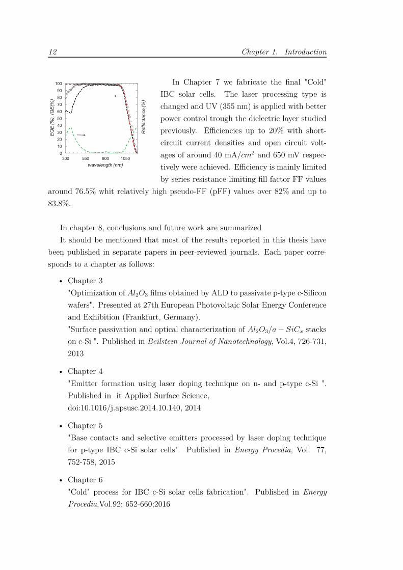
In Chapter 7 we fabricate the final "Cold"
IBC solar cells. The laser processing type is
changed and UV (355 nm) is applied with better
power control trough the dielectric layer studied
previously. Efficiencies up to 20% with short-
circuit current densities and open circuit volt-
ages of around 40 mA/cm2 and 650 mV respec-
tively were achieved. Efficiency is mainly limited
by series resistance limiting fill factor FF values
around 76.5% whit relatively high pseudo-FF (pFF) values over 82% and up to
83.8%.
In chapter 8, conclusions and future work are summarized
It should be mentioned that most of the results reported in this thesis have
been published in separate papers in peer-reviewed journals. Each paper corre-
sponds to a chapter as follows:
• Chapter 3
"Optimization of Al2O3 films obtained by ALD to passivate p-type c-Silicon
wafers". Presented at 27th European Photovoltaic Solar Energy Conference
and Exhibition (Frankfurt, Germany).
"Surface passivation and optical characterization of Al2O3/a − SiCx stacks
on c-Si ". Published in Beilstein Journal of Nanotechnology, Vol.4, 726-731,
2013
• Chapter 4
"Emitter formation using laser doping technique on n- and p-type c-Si ".
Published in it Applied Surface Science,
doi:10.1016/j.apsusc.2014.10.140, 2014
• Chapter 5
"Base contacts and selective emitters processed by laser doping technique
for p-type IBC c-Si solar cells". Published in Energy Procedia, Vol. 77,
752-758, 2015
• Chapter 6
"Cold" process for IBC c-Si solar cells fabrication". Published in Energy
Procedia,Vol.92; 652-660;2016
Bibliography 13
Bibliography
[1] EPIA European Photovoltaic Industry Association. Global market outlook
for photovoltaics 2014-2018, www.solarpowereurope.org, 2014.
[2] Solar Power. Global market outlook 2015-2019, www.solarpowereurope.org,
2015.
[3] IEA International Energy Agency. Technology roadmap-solar photovoltaic
energy, www.iea.org, 2014.
[4] http://pv.energytrend.com/pricequotes.html, 2015.
[5] Fraunhofer Institute for Solar Energy Systems ISE. Photovoltaics report,
www.ise.fraunhofer.de/de/downloads/pdf-files/aktuelles/photovoltaics-
report-in-englischer-sprache.pdf, 2015.
[6] IHS Technology. Top solar power industry trends for
2015, www.ihs.com/pdf/top-solar-power-industry-trends-for-2015-
213963110915583632.pdf, 2015.
[7] G. Dingemans and W. M. M. Kessels. Status and prospects of Al2O3-based
surface passivation schemes for silicon solar cells. Journal of Vacuum Science
and Technology A: Vacuum, Surfaces, and Films, 30:040802, 2012.
[8] A. W. Y. Ho and Stuart R. Wenham. Buried contact solar cells with in-
novative rear localised contacts. Progress in Photovoltaics: Research and
Applications, 12:297–308, 2004.
[9] E. Schneiderlöchner, R. Preu, R. Lüdemann, and S. W. Glunz. Laser-fired
rear contacts for crystalline silicon solar cells. Progress in Photovoltaics:
Research and Applications, 10:29–34, 2002.
[10] D. Carrió, P. Ortega, I. Martín, G. López, J. M. López-González, A. Orpella,
C. Voz, and R. Alcubilla. Rear Contact Pattern Optimization based on 3D
Simulations for IBC Solar Cells with Point-like Doped Contacts. Energy
Procedia, 55:47–52, 2014.
[11] I. Martín, P. Ortega, M. Colina, A. Orpella, G. López, and R. Alcubilla.
Laser processing of Al2O3 /a-SiCx:H stacks: a feasible solution for the rear
14 Bibliography
surface of high-efficiency p-type c-si solar cells. Progress in Photovoltaics:
Research and Applications, 21:1171–1175, 2012.
[12] Pirozzi L., Vetrella U.B, Falconieri M., and Salza E. A laser system for
silicon solar cell processing: design, setup and operation. Materials Science
Forum, pages 319–324, 1995.
[13] Pirozzi L., Vetrella U.B, and Salza E. Innovative applications of laser tech-
nology in photovoltaics. In Proc. SPIE Conf. Laser Applications in Micro-
electronic and Optoelectronic Manufacturing II, 1997.
[14] A. Knorz, M. Peters, A. Grohe, C. Harmel, and R. Preu. Selective laser
ablation of SiNx layers on textured surfaces for low temperature front side
metallizations. Progress in Photovoltaics: Research and Applications, 17:
127–136, 2009.
[15] G. B. Turner. Solar cells made by laser-induced diffusion directly from phos-
phine gas. Applied Physics Letters, 39:967, 1981.
[16] D. Kray, A. Fell, S. Hopman, K. Mayer, G. P. Willeke, and S. W. Glunz.
Laser Chemical Processing (LCP). a versatile tool for microstructuring ap-
plications. Applied Physics A, 93:99–103, 2008.
[17] E. Fogarassy. Silicon solar cells realized by laser induced diffusion of vacuum-
deposited dopants. Journal of Applied Physics, 52:1076, 1981.
[18] M. Colina, I. Martín, C. Voz, A. Morales-Vilches, P. Ortega, G. López,
A. Orpella, R. Alcubilla, I. Sánchez-Aniorte, and C. Molpeceres. Optimiza-
tion of laser doping processes for the creation of p+ regions from solid dopand
sources. In 27 th EUPVSEC, pages 1885–1889, 2012.
[19] I. Martín, M. Colina, A. Orpella, C. Voz, S. De Vecchi, T. Desrues, S. Abol-
masov, P. Roca i Cabarrocas, and R. Alcubilla. Low recombination n+ re-
gions created by n+ c-si epitaxial layers and laser processing of phosphorus-
doped SiCx films. In 27th European Photovoltaic Solar Energy Conference
and Exhibition, pages 1519–1523, 2012.
[20] A. Morales-Vilches, C. Voz, M. Colina, G. Lopez, I. Martin, A. Orpella,
J. Puigdollers, M. Garcia, and R. Alcubilla. Progress in silicon heterojunction
Bibliography 15
solar cell fabrication with rear laser-fired contacts. In Proceedings of the 2013
Spanish Conference on Electron Devices, CDE 2013, pages 345–348, 2013.
[21] A.B. Morales-Vilches, C. Voz, M. Colina, D. Munoz-Martin, I. Martin, P. R.
Ortega, G. Lopez-Rodriguez, C. Molpeceres, and R. Alcubilla. Study of the
surface recombination velocity for ultraviolet and visible laser-fired contacts
applied to silicon heterojunction solar cells. IEEE Journal of Photovoltaics,
5:1006–1013, 2015.
[22] P. Ortega, I. Martín, G. Lopez, M. Colina, A. Orpella, C. Voz, and R. Alcu-
billa. p-type c-Si solar cells based on rear side laser processing of Al2O3/SiCx
stacks. Solar Energy Materials and Solar Cells, 106:80–83, 2012.
[23] J. M. López-González, I. Martín, P. Ortega, A. Orpella, and R. Alcubilla.
Numerical simulations of rear point-contacted solar cells on 2.2 ohm.cm p-
type c-si substrates. Progress in Photovoltaics: Research and Applications,
23:69–77, 2013.
[24] I. Martín, M. Colina, G. Coll, A.and López, P. Ortega, A. Orpella, and
R. Alcubilla. c-si solar cells based on laser-processed dielectric films. Energy
Procedia, 55:255–264, 2014.
[25] G. López, P. Ortega, M. Colina, C. Voz, I. Martín, A. Morales-Vilches,
A. Orpella, and R. Alcubilla. Emitter formation using laser doping technique
on n- and p-type c-si substrates. Applied Surface Science, 2014.
[26] K. Masuko, M. Shigematsu, T. Hashiguchi, D. Fujishima, M. Kai,
N. Yoshimura, T. Yamaguchi, Y. Ichihashi, T. Mishima, N. Matsubara,
T. Yamanishi, T. Takahama, M. Taguchi, E. Maruyama, and S. Okamoto.
Achievement of more than 25% conversion efficiency with crystalline silicon
heterojunction solar cell. IEEE Journal of Photovoltaics, 4:1433–1435, 2014.
[27] P. Ortega, E. Calle, G. von Gastrow, P. Repo, D. Carrió, H. Savin, and R. Al-
cubilla. High-efficiency black silicon interdigitated back contacted solar cells
on p-type and n-type c-si substrates. Progress in Photovoltaics: Research
and Applications, 2015.
[28] H. Savin, P. Repo, G. von Gastrow, P. Ortega, E. Calle, M. Garín, and R. Al-
cubilla. Black silicon solar cells with interdigitated back-contacts achieve
22.1% efficiency. Nature Nanotechnology, 10:624–628, 2015.

Chapter 2
Fundamental Background
In this chapter we present some basic concepts of silicon solar cells.
We merely focus on fundamental definitions in order to understand
how solar cells work. Additionally, back-contact solar cells and state-
of-the-art technology are also described as well as the critical draw-
backs involved with IBC solar cell concept. A general overview and
a short theoretical background of the methods and equipment used in
this thesis are reported.
2.1 Fundamental parameters of solar cells
2.1.1 Introduction
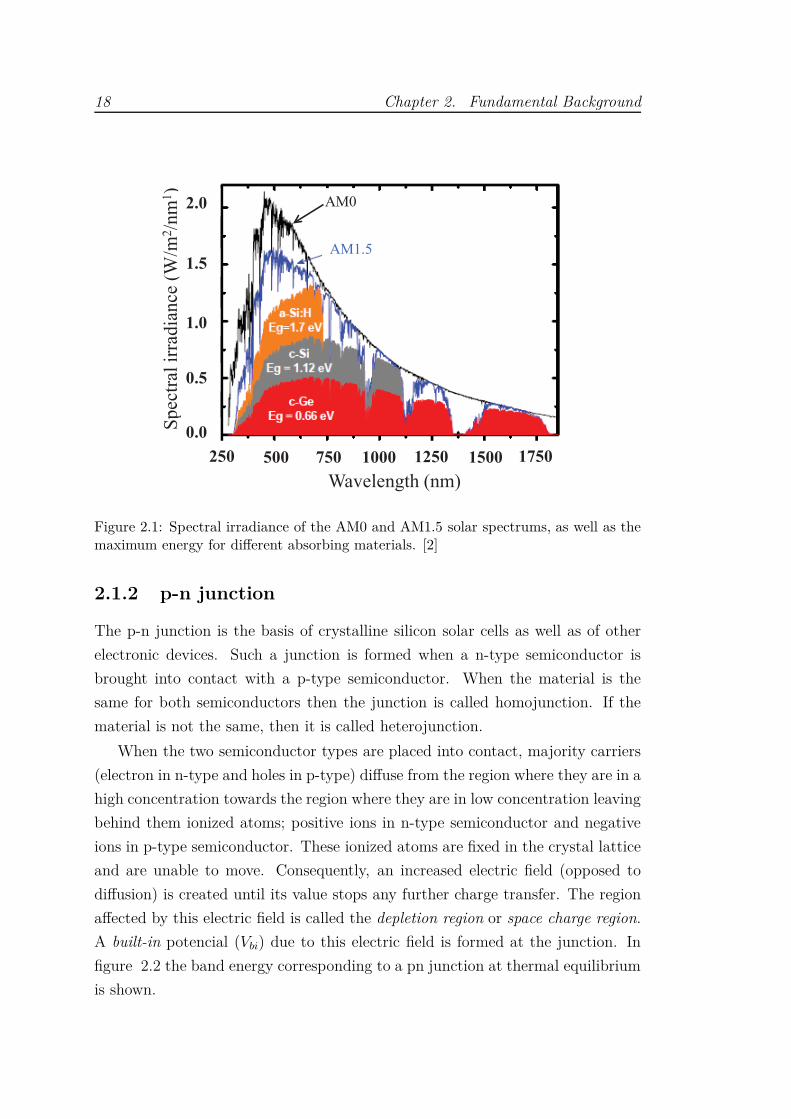
In the photovoltaic effect, the energy of a photon is transferred to charge carriers
i.e. converted into electrical energy. In figure 2.1 we plot the AM01 and AM1.52
spectral irradiance corresponding to the spectrum used as a reference by the
spatial industry and photovoltaic earth applications respectively.
The thermodinamic limit of the conversion efficiency for a single band-gap of
c-Si (1.12 eV) under AM1.5G solar spectrum and taking into intrinsic recombi-
nation was found to be 29.4% [1].
In figure 2.1 in grey color we can see the fraction of the spectrum that can be
converted to electrical energy by a single-junction silicon solar cell. Others ab-
sorbing materials used in PV field are also shown for comparison.
1http://rredc.nrel.gov/solar/spectra/am02http://rredc.nrel.gov/solar/spectra/am1.5
17
18 Chapter 2. Fundamental Background
Wavelength (nm)
Sp
ectr
al i
rrad
ian
ce (
W/m
2/n
m1)
0.0
0.5
1.0
1.5
2.0
250 500 750 1000 1250 1500 1750
AM0
AM1.5
Figure 2.1: Spectral irradiance of the AM0 and AM1.5 solar spectrums, as well as themaximum energy for different absorbing materials. [2]
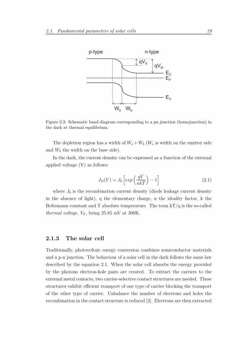
2.1.2 p-n junction
The p-n junction is the basis of crystalline silicon solar cells as well as of other
electronic devices. Such a junction is formed when a n-type semiconductor is
brought into contact with a p-type semiconductor. When the material is the
same for both semiconductors then the junction is called homojunction. If the
material is not the same, then it is called heterojunction.
When the two semiconductor types are placed into contact, majority carriers
(electron in n-type and holes in p-type) diffuse from the region where they are in a
high concentration towards the region where they are in low concentration leaving
behind them ionized atoms; positive ions in n-type semiconductor and negative
ions in p-type semiconductor. These ionized atoms are fixed in the crystal lattice
and are unable to move. Consequently, an increased electric field (opposed to
diffusion) is created until its value stops any further charge transfer. The region
affected by this electric field is called the depletion region or space charge region.
A built-in potencial (Vbi) due to this electric field is formed at the junction. In
figure 2.2 the band energy corresponding to a pn junction at thermal equilibrium
is shown.
2.1. Fundamental parameters of solar cells 19
Figure 2.2: Schematic band diagram corresponding to a pn junction (homojunction) inthe dark at thermal equilibrium.
The depletion region has a width of We + Wb (We is width on the emitter side
and Wb the width on the base side).
In the dark, the current density can be expressed as a function of the external
applied voltage (V) as follows:
JD(V ) = J0
[
exp(
qV
nkT
)
− 1]
(2.1)
where J0 is the recombination current density (diode leakage current density
in the absence of light), q the elementary charge, n the ideality factor, k the
Boltzmann constant and T absolute temperature. The term kT/q is the so-called
thermal voltage, VT , being 25.85 mV at 300K.
2.1.3 The solar cell
Traditionally, photovoltaic energy conversion combines semiconductor materials
and a p-n junction. The behaviour of a solar cell in the dark follows the same law
described by the equation 2.1. When the solar cell absorbs the energy provided
by the photons electron-hole pairs are created. To extract the carriers to the
external metal contacts, two carrier-selective contact structures are needed. These
structures exhibit efficient transport of one type of carrier blocking the transport
of the other type of carrier. Unbalance the number of electrons and holes the
recombination in the contact structure is reduced [3]. Electrons are then extracted

20 Chapter 2. Fundamental Background
by metal contacts to an external circuit where dissipate its energy and return to
the solar cell. Consequently, a good ohmic contact is required. This flow of
carriers is called photogenerated current.
In short-circuit conditions the carriers are injected to the external circuit
generating a current (Jsc, short-circuit current density). When the solar cell
works under open-circuit conditions the junction energy barrier height decreases.
Consequently, the minority diffusion currents increase in such a way that perfectly
cancel the photogenerated current leading to no external current, i.e. open-circuit
conditions. The voltage required to achieve at this equilibrium is called open-
circuit voltage, Voc. To understand the electrical properties of a solar cell, it
is useful to create a model which is electrically equivalent and based on discrete
electrical components. This model describes an illuminated solar cell and includes
the initial diode and the photogenerated current density (Jph) flowing in the
opposite direction, as it is shown in figure 2.3.
Rs
Rsh
JPh
V
JJD
+
_
Figure 2.3: Electrical model used to describe a solar cell.
The electrical model above described also includes parasitic series resistance
(RS) that takes into account all the resistive losses in the solar cell (e.g. contact
resistance, emitter and base resistance, metallization grid ohmic losses, etc.) and
shunt resistance (Rsh) causing efficiency drops. Equation 2.2 describes electrical
behaviour considering ohmic losses where, rs and rsh are the normalized resis-
tances considering the cell area in (Ωcm2) units.
J(V ) = J0[exp(q(V − rsJ)
nKT) − 1] +
V − rsJ
rsh− Jph (2.2)
2.1. Fundamental parameters of solar cells 21
Losses caused by series resistance increase, in a first approximation, quadrati-
cally with the photocurrent. Series resistance losses are therefore most important
at high illumination intensities and have to be kept as low as possible. As se-
ries resistance increases, the terminal voltage significantly decreases. The short-
circuit current, is slightly affected but very high values of Rs could also produce
a significant reduction of this parameter.
Low shunt resistance produces a significant reduction in the terminal current
and a slight reduction in Voc. Although very low values of Rsh could also signifi-
cantly reduce Voc. Obviously, shunt resistance has to be kept as high as possible.
Very high series resistance or/and very low shunt resistance produce a solar cell
behaviour similar to those of a resistor.
Physically, reverse saturation current (or recombination current density) is
a measurement of the leakage of carriers across the p-n junction in reverse bias
resulting from the recombination in the neutral regions on either side of the
junction. The increase of Jo leads to a reduction of Voc proportional to the
inverse of the logarithm of the increase.
The ideality factor (n) is a parameter related to the current mechanism do-
minating the J-V curve. The ideality factor n = 1 implies recombination taking
place at the quasi-neutral regions of the diode without recombination within the
space-charge region. On the other hand, when recombination in space-region
dominates then n ∼= 2.
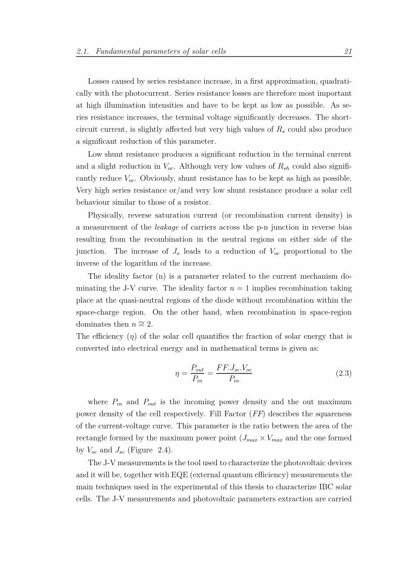
The efficiency (η) of the solar cell quantifies the fraction of solar energy that is
converted into electrical energy and in mathematical terms is given as:
η =Pout
Pin=
FF.Jsc.Voc
Pin(2.3)
where Pin and Pout is the incoming power density and the out maximum
power density of the cell respectively. Fill Factor (FF) describes the squareness
of the current-voltage curve. This parameter is the ratio between the area of the
rectangle formed by the maximum power point (Jmax × Vmax and the one formed
by Voc and Jsc (Figure 2.4).
The J-V measurements is the tool used to characterize the photovoltaic devices
and it will be, together with EQE (external quantum efficiency) measurements the
main techniques used in the experimental of this thesis to characterize IBC solar
cells. The J-V measurements and photovoltaic parameters extraction are carried
22 Chapter 2. Fundamental Background
0
5
10
15
20
25
30
35
40
0 0,2 0,4 0,6
Cu
rren
t d
ensi
ty [
mA
/cm
2]
V [V]
JscxVoc
JmaxxVmax
Jsc
Voc
Jmax
Vmax
Figure 2.4: Typical J-V curve of a solar cell
out under standard test conditions, i.e. AM1.5G 1 KW/m2 Solar spectrum and
T = 25 °C.
Dark measurements allow to determine J0 and n parameters while under illu-
mination conditions we get information of Voc, Jsc and FF, as well as solar cell
efficiency.
2.1.4 Intrinsic losses limitations
The conversion efficiency in a c-Si solar cell is limited in a first approximation by
the following intrinsic and unavoidable loss mechanisms:
• Photons with energy higher than the bandgap energy of the material (1.12
eV) will generate electron-hole pairs. However, the exceeding energy will
be lost due to thermalization process. This means that the electron will be
promoted from valence band to conduction band at an energy level higher
than the edge of conduction band. These hot electrons release its extra
energy via phonon scattering in a very short time compared to the one
needed to collect them.
• Photons with smaller energy than the bandgap of silicon will not be ab-
sorbed by the material. The photon energy will not be enough to generate
electron-hole pairs and its energy will be lost.

2.2. Review of back-contact silicon solar cells 23
• Absorption coefficient of the silicon strongly depends on the photon wave-
length. For photons with wavelength higher than 1000 nm the absorption
coefficient is very low resulting in absorption lengths longer than device
thickness. Then, depending on light-trapping properties, these photons can
escape from the device without being absorbed, despite of having the ap-
propriate energy to generate electron-hole pairs.
• The finite maximal average path length of the photons within the silicon
is an intrinsic optical loss effect which limits the short-circuit current (Jsc)
of a solar cell. This maximal average path length (l), considering optimal
light trapping scheme, can be approximated by [4],[5]:
l ≈ 4 × nSi(λ) × W (2.4)
where nSi(λ) is the refraction index of the silicon as a function of the wave-
length and W is the wafer thickness.
Take into account equation 2.4 and the AM1.5G spectrum, the Jsc limit for
a silicon wafer thickness of 280 µn is calculated about 43.8 mA/cm2. [6].
• Open-circuit voltage (Voc) of solar cell is limited by the recombination rate
of the electrons and holes. Intrinsic recombination are radiative and Auger
recombination (explained in detail in chapter 3 (3.2.1 and 3.2.2). A detailed
study of the limit of the open-circuit voltage calculated for different wafer
thicknesses and different base doping density of an n and p-type solar cell
can be found in the thesis work realized by Kerr [6].
All the intrinsic loss mechanisms above explained determine the maximum
light-electricity conversion to be achieved by a solar cell, resulted to be about
28.5% ([6]). However, this efficiency will be even more reduced due to technolog-
ical issues related to solar cell processing.
2.2 Review of back-contact silicon solar cells
Conventional solar cells have metal contacts on both cell sides. The best example
of this architecture is the so-called Passivated Emitter Rear Locally diffussed
(PERL) cell (see figure 2.5). This structure enabled reaching at 25% of efficiency

24 Chapter 2. Fundamental Background
of monocrystalline (homojunction) silicon solar cell under one-sun illumination
intensity [7]. The features of this cell are:
• A selective doping profiles underneath metal contacts for low contact re-
combination
• Passivated front and rear surfaces
• Well textured front surface with an antireflection coating for low front sur-
face reflection
• A flat, highly reflective rear for light-trapping
• Low front contact shading
Rear contact oxide
finger “inverted” pyramids
Figure 2.5: The passivated emitter, rear locally-diffused PERL cell. Record efficiencyof 25%
These features are required for high-efficiency PERL solar cells but also are re-
quired for the back-contact back-junction cell structure. However, the full PERL
design is not easy to apply to low-cost industrial production because of the necessi-
ty for multiple photolithography steps. On the other hand, a trade-off between
resistive losses and optical shading losses due to the front metal grid have to be
considered. Such a problem is partially or totally overcame using back contact
structures.

2.2. Review of back-contact silicon solar cells 25
Back contact cell design is not a recent concept. Since the first publications
by R.J. Schwartz in 1975 [8], interest in back-contact cells has been growing in
the last years. Two major advantages which make these cells of great interest are
a lack of grid shading loss and a coplanar interconnection.
In April 2014 Panasonic achieved the world’s highest energy conversion effi-
ciency of 25.6% at research level (147.7 cm2) [9]. This new record is an improve-
ment of 0.6 points over the previous record for small area crystalline silicon-based
solar cells of 25% (University of New South Wales (Australia)) [10]. Even more
recently, in September 2016, Kaneka Corporation has announced a 26.3% of effi-
ciency. This achievement was possible by further development of its heterojunc-
tion technology adopted to a back-contact solar cell structure which allows the
more efficient utilization of the sunlight.
Back-contact cells developed to date can be divided into three categories:
• Metallization Wrap Through (MWT) solar cells
• Emitter Wrap Through (EWT) solar cells
• Back-Contact Back-Junction (BC-BJ) solar cells, also called Interdigitated
Back Contact (IBC) solar cells
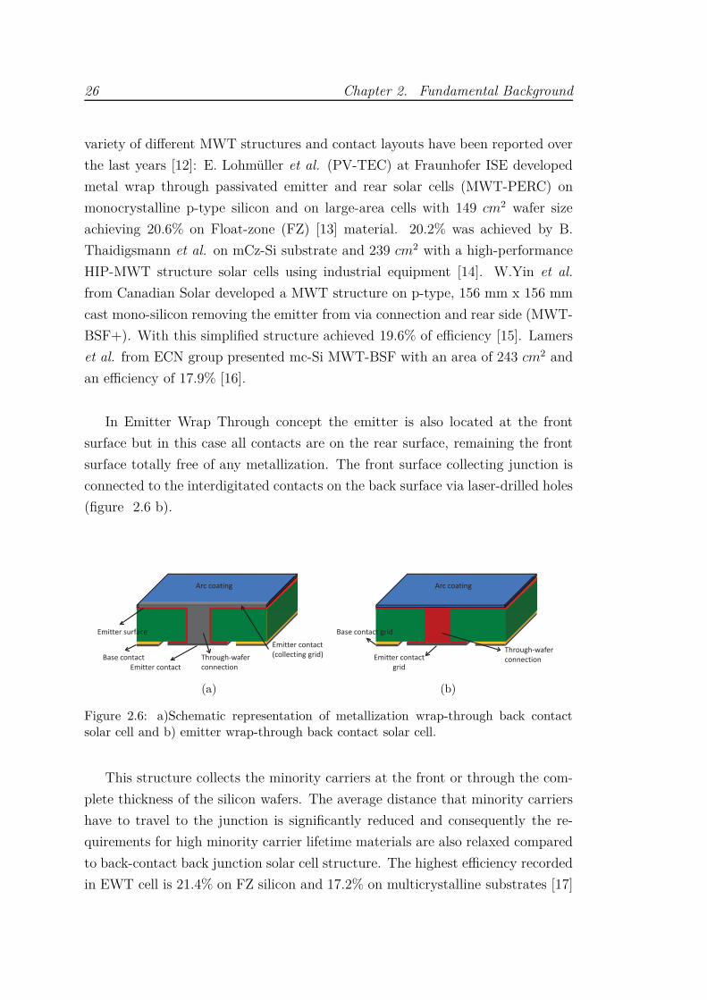
2.2.1 Metallization and Emitter Wrap Through (MWT
and EWT) solar cells
Metallization wrap-through back-contact cell [11] is the concept that is most clo-
sely linked to the conventional cell structure (Figure 2.5). In both cell structures
the emitter is located at the front surface, but in the former part of the front
metallisation grid is moved from the front to the rear surface. The front side
metal fingers are interconnected to the busbar placed at the rear side through
the laser drilled holes in the wafer (figure 2.6 a). The MWT cell concept offers
some advantages over the conventional solar cell. Removing the busbar from
the front side, front contact shading is reduced. Simultaneously, the coplanar in-
terconnection is possible since both contact polarities are placed on the back side.
Many highly efficient metal wrap through solar cell types on monocrystalline
p-type and n-type silicon with efficiencies of about 20% have been reported and a
26 Chapter 2. Fundamental Background
variety of different MWT structures and contact layouts have been reported over
the last years [12]: E. Lohmüller et al. (PV-TEC) at Fraunhofer ISE developed
metal wrap through passivated emitter and rear solar cells (MWT-PERC) on
monocrystalline p-type silicon and on large-area cells with 149 cm2 wafer size
achieving 20.6% on Float-zone (FZ) [13] material. 20.2% was achieved by B.
Thaidigsmann et al. on mCz-Si substrate and 239 cm2 with a high-performance
HIP-MWT structure solar cells using industrial equipment [14]. W.Yin et al.
from Canadian Solar developed a MWT structure on p-type, 156 mm x 156 mm
cast mono-silicon removing the emitter from via connection and rear side (MWT-
BSF+). With this simplified structure achieved 19.6% of efficiency [15]. Lamers
et al. from ECN group presented mc-Si MWT-BSF with an area of 243 cm2 and
an efficiency of 17.9% [16].
In Emitter Wrap Through concept the emitter is also located at the front
surface but in this case all contacts are on the rear surface, remaining the front
surface totally free of any metallization. The front surface collecting junction is
connected to the interdigitated contacts on the back surface via laser-drilled holes
(figure 2.6 b).
Through-wafer
connection
Arc coating
Emitter contact
(collecting grid)
Emitter surface
Emitter contact
Base contact
(a)
Through-wafer
connection
Arc coating
Emitter contact
grid
Base contact grid
(b)
Figure 2.6: a)Schematic representation of metallization wrap-through back contactsolar cell and b) emitter wrap-through back contact solar cell.
This structure collects the minority carriers at the front or through the com-
plete thickness of the silicon wafers. The average distance that minority carriers
have to travel to the junction is significantly reduced and consequently the re-
quirements for high minority carrier lifetime materials are also relaxed compared
to back-contact back junction solar cell structure. The highest efficiency recorded
in EWT cell is 21.4% on FZ silicon and 17.2% on multicrystalline substrates [17]

2.2. Review of back-contact silicon solar cells 27
2.2.2 Back-contact back-junction (BC-BJ) solar cells
In Back-contact back-junction solar cell (figure 2.7), the collecting junction to-
gether with both contacts are located on the back side of the cell, commonly
designed forming an interdigitated (IBC) pattern. A special attention will be
given to this structure type since it will be the main topic of this thesis.
Monocrystalline Si (Cz n-type, textured)
n-type a-Si
Passivation layer
i-type a-Si
p-type a-Si
Grid electrodes
Figure 2.7: Structure of c-Si HIT solar cell with interdigitated back contact. Panasonic,2014
This structure, as in EWT solar cells, eliminates the front surface contact
reflection and exhibit the following advantages.
• Higher Jsc of the cell due to the absence of the front metal grid to shadow
the incident photon flux. Zero shading.
• As a consequence of the absence of the front metal grid, the front surface can
be optical and electrically optimized (i.e. light trapping and surface passi-
vation improvements) without the constrains imposed by the conventional
trade-off between reflection and series resistance found in front-contacted
solar cells.
• Series resistance can be substantially reduced because the backside metal-
lization pattern width is not limited by the shading losses and it can cover
nearly half of the back surface for each type of polarization.
28 Chapter 2. Fundamental Background
• BC-BJ solar cells are well suited for tandem solar cells as bottom cells. The
metal-free front surface can be used for epitaxial growth of the top cells or
even just as a holder in four terminal configuration.
• Easier co-planar interconnection in the module and increases of the solar
cell packaging density.
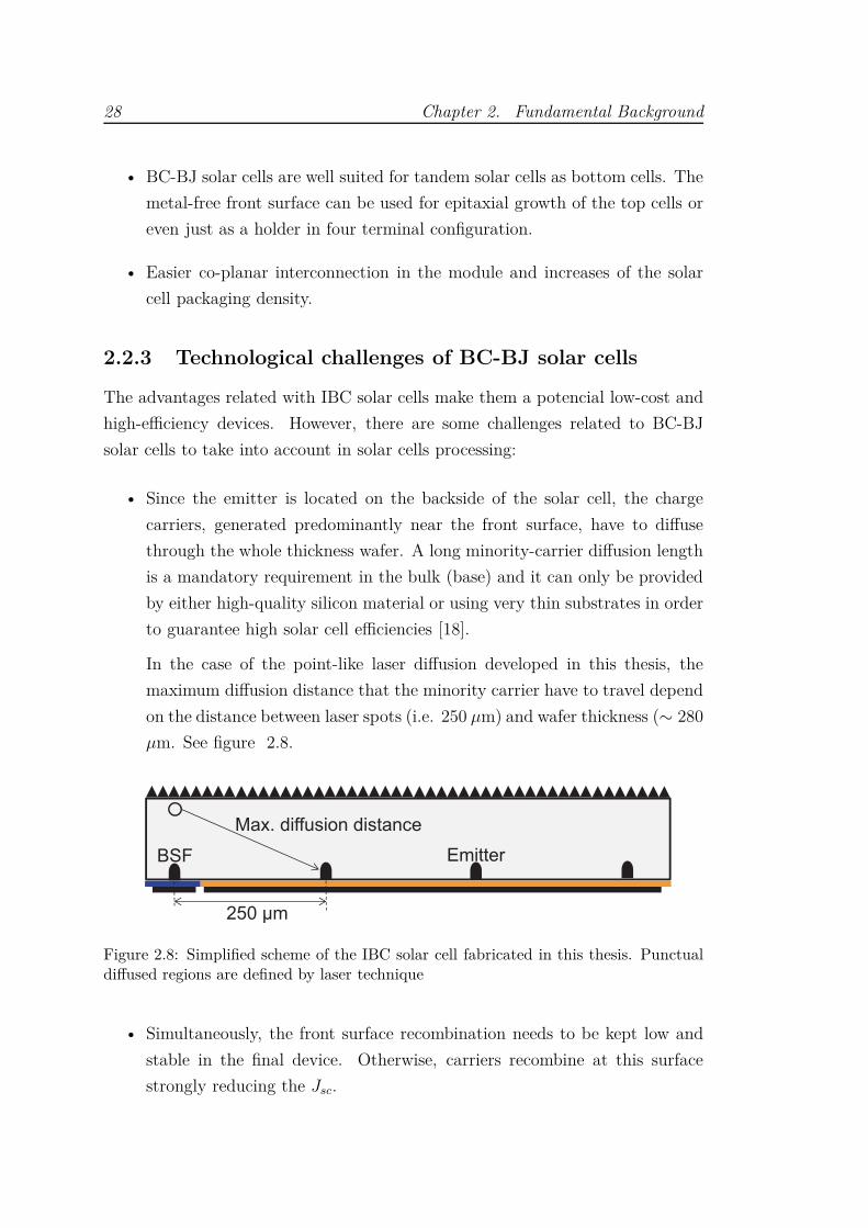
2.2.3 Technological challenges of BC-BJ solar cells
The advantages related with IBC solar cells make them a potencial low-cost and
high-efficiency devices. However, there are some challenges related to BC-BJ
solar cells to take into account in solar cells processing:
• Since the emitter is located on the backside of the solar cell, the charge
carriers, generated predominantly near the front surface, have to diffuse
through the whole thickness wafer. A long minority-carrier diffusion length
is a mandatory requirement in the bulk (base) and it can only be provided
by either high-quality silicon material or using very thin substrates in order
to guarantee high solar cell efficiencies [18].
In the case of the point-like laser diffusion developed in this thesis, the
maximum diffusion distance that the minority carrier have to travel depend
on the distance between laser spots (i.e. 250 µm) and wafer thickness (∼ 280
µm. See figure 2.8.
Figure 2.8: Simplified scheme of the IBC solar cell fabricated in this thesis. Punctualdiffused regions are defined by laser technique
• Simultaneously, the front surface recombination needs to be kept low and
stable in the final device. Otherwise, carriers recombine at this surface
strongly reducing the Jsc.

2.2. Review of back-contact silicon solar cells 29
• Back surface passivation quality is also needed to avoid carrier recombina-
tion. Furthermore, the rear surface hosts the extended termination of the
junction and the Voc and the FF of the cell can be lowered by the contribu-
tion of the second diode recombination current due to a space-charge region
surface recombination [19].
• Surface conductance channels can be formed between the emitter and the
base contacts when dielectric layers are applied for passivation schemes
based on surface field in the silicon. Thermal SiO2 or densified deposited
oxide are good options [20],[21].
• The processing of back-contact solar cells requires several patterning steps
resulting in a complex fabrication process.
• The closely spaced interdigitated fingers of opposite polarity on the backside
of the cell, requires careful alignment to avoid risk of fatal shunting between
the p- and n- electrodes.
Recombination in the contact areas become dominant once the base lifetime
is sufficiently high and all the surfaces are well passivated. Reducing the contact
fraction helps to reduce this recombination and the point contact cell is the best
way to achieve it [22],[23]. The point-contact structure consists of the alternating
n- and p-regions in an array pattern on the bottom surface of the device. The IBC
solar cells fabricated in this thesis follow this structure (see figure 2.8) and the
point-contact base and emitter are formed by laser processing through dielectric
layer as it will be explained in chapter 4.
The reduction of the recombination in the contact areas by reducing the
fraction results in an increased open-circuit voltage. However, the collection of
minority-carrier is also reduced and consequently the short-circuit current and/or
fill factor [24],[25]. An accurate solar cell design is needed in order to optimize
the trade-off between the improvement of the Voc and the reduction of Jsc and
FF. On the other hand, by reducing the area of the highly diffused regions, the
dark saturation current of the doped areas could be also reduced significantly.
With this idea in mind our group at the UPC (MNT, Micro and Nanotechnolo-
gies) has carefully designed and simulated different rear point-contact patterns to
be implemented in IBC solar cell, giving a first approximation to the fabrication
of our first IBC solar cell [26],[27].
30 Chapter 2. Fundamental Background
2.3 State-of the art of BC-BJ solar cells
The first BC-BJ silicon solar cell concept suggested by Schwarts and Lammert in
1975 (Stanford University) was originally focused for concentrator applications
and the emitter and base were thermally diffused and arranged in an interdig-
itated pattern. This first version reported an efficiency of 17% under 50 suns
concentration. An improved version of the point-contact cell of Swanson et al.
where the backside diffusion were arranged in arrays of single points [22] was
performed by Sinton et al. demonstrating an efficiency of 28.4% under 200 suns
concentration [28] in 1987. The area of these cells was 0.15 cm2.
The back-contact back-junction solar cell structure was also optimized for
applications under one-sun illumination standard reporting in 1985 an efficiency
of 21% [29]. One year later Sinton et al. introduced a point contact solar cell
with 21.7%. King et al. presented a first medium-area (8.5 cm2) point contact
solar cell with the front and back surface field and a novel multi-level metal-
lization scheme introduced by Verlinden et al. [30] [31]. In 1990 Sinton et al.
presented a simplified back-side solar cell [32] in which the self-aligment method
was applied [33] and the masking step was reduced to one. An efficiency of 21.9%
was reported for a 10.5 cm2 and one-sun illumination. Sunpower Corporation
(founded in 1985) commercialized the back-contact silicon solar cells developed
by the research group of Stanford University. In 1997 reported a new record one-
sun efficiency of 23.2% resulting from the edge passivation and substrate doping
improvements [34]. In 2004 Mulligan et al. presented a manufacture of large-
area (149 cm2) back-contact solar cells (A-300) with a 21.5% of efficiency [35].
New generation of a high volume production of the A-300 was introduced by De
Ceuster el al. in 2007 [36].
Additionally to Stanford University and Sunpower, other groups have simul-
taneously been working on the high-efficiency back-contact back-junction solar
cells devices. The Fraunhofer ISE processed a rear-contacted silicon solar cells
with line contacts and photolithography masking reporting an efficiency of 22.1%
[37]. From UNSW, Guo developed in 2004 the Interdigitated Backside Buried
Contact (IBBC), a low-cost approach without the use of photolithography. A
maximum one-sun efficiency of 19.2% was obtained [38]. Engelhart et al. from
ISFH developed between 2006-07 a low-cost BC-BJ solar cells fabricated using a
mask-free process in witch the laser ablation of Si and laser ablation of protective
2.3. State-of the art of BC-BJ solar cells 31
coating were applied. 22% of efficiency was achieved on 4 cm2 laboratory solar
cell [39].
Interdigitated back contact solar cell has long been widely regarded and nowa-
days with silicon heterojunction (SHJ) technology has surpass the previous world
record efficiency of 25% achieved in silicon single-junction solar cell [40]. Pana-
sonic has recently reported a new record of 25.6% of efficiency combining the SHJ
technique and IBC structure on 143.7 cm2 [41]. The same year, Sharp also re-
ported and efficiency of 25.1% on 4 cm2 based on the same SHJ-IBC architecture
[42]. Last Septembre (2016) Kaneka announced an efficiency of 26.3%. SunPower
reported a 25.2% for its IBC solar cells using more standard surface passivation
methods and manufactured on an industrial pilot line [43]. ANU/Trina and LG
reported and efficiency of 24.4 and 23.4% respectively using thermal diffusion and
SHJ technique in each case [44],[45]. Table 2.1 shows a summary of the state-of-
the-art.
More than twenty years ago, our research group (MNT,UPC) started its ad-
venture in the solar cell world. Among others, a research line of PERC-solar
cells was developed, concluding with an excellent 21% of efficiency. The PERC
solar cell developed was backside passivated with Al2O3 and rear contacted by
laser processing [46]. Other important developments in a − Si/a − SiCx, laser
doping technique and heterojunction solar cells contributed to group solar cell
knowledge.
Five years ago, the MNT group started its research in IBC-BJ solar cells.
Since then, many focus of interest have opened different research lines. Conven-
tional diffused IBC, "Hybrid" IBC, "Cool" IBC, IBC based on carrier-selective
heterocontacts (TMO's, T iO2, Tunnel oxides and alkaline metal salts). Today,
an excellent 22% of efficiency have been obtained in conventional diffused IBC
solar cells improved with a front surface black-silicon textured [47], a 20.8% effi-
ciency in n-type "Hybrid" IBC [48]. The work of this thesis has contributed with
a 18.8% of efficiency in p-type "Hybrid" IBC, with a 18% in our first "Cold" IBC
[49] (laser IR) and with a 20% of efficiency in the last "Cold" IBC cells developed
with UV laser.
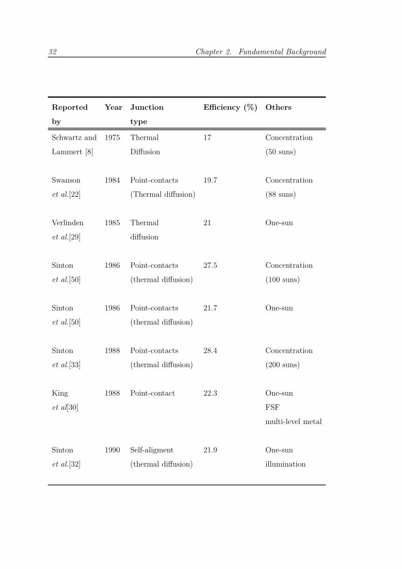
32 Chapter 2. Fundamental Background
Reported Year Junction Efficiency (%) Others
by type
Schwartz and 1975 Thermal 17 Concentration
Lammert [8] Diffusion (50 suns)
Swanson 1984 Point-contacts 19.7 Concentration
et al.[22] (Thermal diffusion) (88 suns)
Verlinden 1985 Thermal 21 One-sun
et al.[29] diffusion
Sinton 1986 Point-contacts 27.5 Concentration
et al.[50] (thermal diffusion) (100 suns)
Sinton 1986 Point-contacts 21.7 One-sun
et al.[50] (thermal diffusion)
Sinton 1988 Point-contacts 28.4 Concentration
et al.[33] (thermal diffusion) (200 suns)
King 1988 Point-contact 22.3 One-sun
et al[30] FSF
multi-level metal
Sinton 1990 Self-aligment 21.9 One-sun
et al.[32] (thermal diffusion) illumination

2.3. State-of the art of BC-BJ solar cells 33
Reported Year Junction Efficiency (%) Others
by type
King 1991 Point-contacts 22.7 One-sun
et al.[51] FSF illumination
multi-level metal
Verlinden 1997 Point-contacts 23.4 One-sun
et al.[34] (thermal diffusion) illumination
Dicker (ISE) 2002 line contacts 22.1 One-sun
et al.[37] (thermal diffusion) (illumination)
Guo 2004 Buried contacts 19.2 One-sun
(UNSW)[38] (thermal diffusion) illumination
Mohr 2005 line contacts 25 Concentration
(ISE)[52] (thermal diffusion) (100 suns)
Engelhart 2006 Laser ablation 22 One-sun
et al [39] (thermal diffusion) illumination
(ISFH)
ANU/Trina[44] 2013 Thermal diffusion 24.4 one-sun
illumination
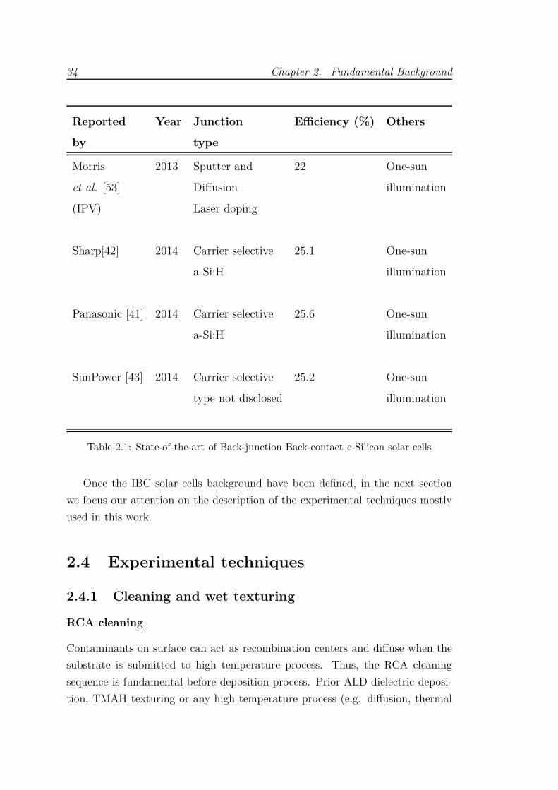
34 Chapter 2. Fundamental Background
Reported Year Junction Efficiency (%) Others
by type
Morris 2013 Sputter and 22 One-sun
et al. [53] Diffusion illumination
(IPV) Laser doping
Sharp[42] 2014 Carrier selective 25.1 One-sun
a-Si:H illumination
Panasonic [41] 2014 Carrier selective 25.6 One-sun
a-Si:H illumination
SunPower [43] 2014 Carrier selective 25.2 One-sun
type not disclosed illumination
Table 2.1: State-of-the-art of Back-junction Back-contact c-Silicon solar cells
Once the IBC solar cells background have been defined, in the next section
we focus our attention on the description of the experimental techniques mostly
used in this work.
2.4 Experimental techniques
2.4.1 Cleaning and wet texturing
RCA cleaning
Contaminants on surface can act as recombination centers and diffuse when the
substrate is submitted to high temperature process. Thus, the RCA cleaning
sequence is fundamental before deposition process. Prior ALD dielectric deposi-
tion, TMAH texturing or any high temperature process (e.g. diffusion, thermal
2.4. Experimental techniques 35
oxidation) wafers are cleaned following a complete RCA sequence [54].
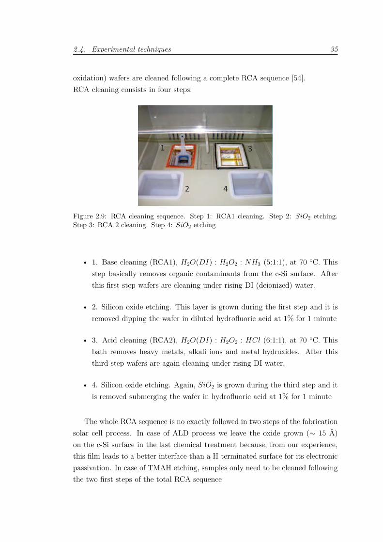
RCA cleaning consists in four steps:
1
2
3
4
Figure 2.9: RCA cleaning sequence. Step 1: RCA1 cleaning. Step 2: SiO2 etching.Step 3: RCA 2 cleaning. Step 4: SiO2 etching
• 1. Base cleaning (RCA1), H2O(DI) : H2O2 : NH3 (5:1:1), at 70 C. This
step basically removes organic contaminants from the c-Si surface. After
this first step wafers are cleaning under rising DI (deionized) water.
• 2. Silicon oxide etching. This layer is grown during the first step and it is
removed dipping the wafer in diluted hydrofluoric acid at 1% for 1 minute
• 3. Acid cleaning (RCA2), H2O(DI) : H2O2 : HCl (6:1:1), at 70 C. This
bath removes heavy metals, alkali ions and metal hydroxides. After this
third step wafers are again cleaning under rising DI water.
• 4. Silicon oxide etching. Again, SiO2 is grown during the third step and it
is removed submerging the wafer in hydrofluoric acid at 1% for 1 minute
The whole RCA sequence is no exactly followed in two steps of the fabrication
solar cell process. In case of ALD process we leave the oxide grown (∼ 15 Å)
on the c-Si surface in the last chemical treatment because, from our experience,
this film leads to a better interface than a H-terminated surface for its electronic
passivation. In case of TMAH etching, samples only need to be cleaned following
the two first steps of the total RCA sequence
36 Chapter 2. Fundamental Background
Wet texturing
Reduction of light reflected from the solar cell surface is of paramount importance
to get high efficiency devices. These reflection losses can be significantly reduced
by application of the so-called antireflection coating (ARC) and/or texturing
the c-Si wafer surface. Random pyramidal texturing is commonly achieved by
chemical anisotropic etching in potassium hydroxide (KOH) or sodium hydroxide
(NaOH) and isopropyl alcohol (IPA), but it can contaminate the surface with K+
and Na+ metal ions . To avoid this contamination, the non-pollutant and non-
toxic alternative used in this work is tetramethyl ammonium hydroxyde (TMAH)
and IPA used as a surfactant to diminish the adherence of hydrogen bubbles to
the etched surface. Figure 2.10(a) illustrates how a pyramidal structure can
reflect incident rays onto a neighbouring pyramid giving the photons two or more
opportunities to be transmitted into the cell’s absorber. Texture also helps ab-
sorption by increasing a cell 's capacity to “trap”reflected light from the rear
surface of the silicon wafer [55].
Conditions applied in this experimental research for texturing c-Si surface are
depicted in the following table. Texturing process is carried out in one silicon
side while the other one remains protected by thermal SiO2.
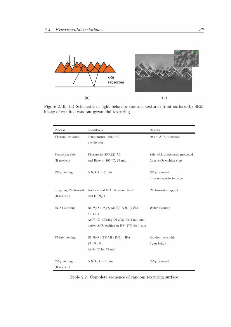
2.4. Experimental techniques 37
c-Si
(absorber)
(a) (b)
Figure 2.10: (a) Schematic of light behavior towards textured front surface.(b) SEMimage of resulted random pyramidal texturing
Process Conditions Results
Thermal oxidation Temperature: 1060 °C 60 nm SiO2 thickness
t = 60 min
Protection side Photoresist SPR220 7.0 Side with photoresist protected
(If needed) and Bake at 105 °C, 15 min from SiO2 etching step
SiO2 etching NH4F t = 2 min SiO2 removed
from non-protected side
Stripping Photoresist Acetone and IPA ultrasonic bath Photoresist stripped
(If needed) and DI H2O
RCA1 cleaning DI H2O : H2O2 (30%): NH3 (25%) Wafer cleaning
6 : 1 : 1
At 75 °C +Rising DI H2O for 5 min and
native SiO2 etching in HF (1%) for 1 min
TMAH etching DI H2O : TMAH (25%) : IPA Random pyramids
83 : 9 : 8 6 µm height
At 80 °C for 73 min
SiO2 etching NH4F , t = 2 min SiO2 removed
(If needed)
Table 2.2: Complete sequence of random texturing surface
38 Chapter 2. Fundamental Background
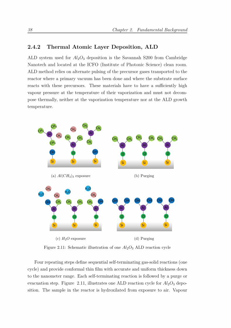
2.4.2 Thermal Atomic Layer Deposition, ALD
ALD system used for Al2O3 deposition is the Savannah S200 from Cambridge
Nanotech and located at the ICFO (Institute of Photonic Science) clean room.
ALD method relies on alternate pulsing of the precursor gases transported to the
reactor where a primary vacuum has been done and where the substrate surface
reacts with these precursors. These materials have to have a sufficiently high
vapour pressure at the temperature of their vaporization and must not decom-
pose thermally, neither at the vaporization temperature nor at the ALD growth
temperature.
CH4
CH4
Si Si Si
OH OH O
Al
CH3 CH3
(a) Al(CH3)3 exposure
Si Si Si
O
Al
CH3 CH3
O O
(b) Purging
Si Si Si
O
Al
O O
OH OH CH3 CH3 CH3 CH3
CH4
CH4 CH4 H2O
H2O H2O
(c) H2O exposure
Si Si Si
O
Al
O O
OH OH OH OH OH OH
(d) Purging
Figure 2.11: Schematic illustration of one Al2O3 ALD reaction cycle
Four repeating steps define sequential self-terminating gas-solid reactions (one
cycle) and provide conformal thin film with accurate and uniform thickness down
to the nanometer range. Each self-terminating reaction is followed by a purge or
evacuation step. Figure 2.11, illustrates one ALD reaction cycle for Al2O3 depo-
sition. The sample in the reactor is hydroxilated from exposure to air. Vapour

2.4. Experimental techniques 39
H20 is adsorbed on the surface and with silicon surface form: Si-O-H. The four
steps defined in the reactor are: (a)Self-terminating reaction of the first reac-
tant. A 0.05 sec pulse of trimethylaluminum ([Al(CH3)3],TMA) (Al precursor)
reacts with hydroxyl groups, -OH. (b) Then a 5 sec of purge or evacuation with
inert N2 removes the non-reacted TMA and gaseous reaction by-products (CH4,
Ammonia). (c) Self-terminating reaction of 0.015 sec of the second reactant
(H2O)(oxygen precursor) reacts with the dangling methyl groups on the new sur-
face, creating aluminium-oxygen (Al-O) bridges an hydroxyl surface groups. (d)
Finally a 5 sec of purge or evacuation with N2 removes non-reacted H2O and
CH4. The amount deposited per cycle (step 1 to 4) is expressed as growth rate,
GPC (Growth per cycle) and is 1.1 Å. Reaction cycles are repeated until the
desired amount of material has been deposited.
2.4.3 Plasma Enhanced Chemical Vapour Deposition,
PECVD
Plasma-enhanced chemical vapour deposition is a subset of chemical vapour de-
position techniques to deposit thin films from vapour phase to solid state on
substrates. Process gas is decomposed aided (enhanced) by a plasma created by
radio-frequency (13.56 MHz) discharge between two flat and parallel electrodes.
In the frame of this work, RF PECVD from Elettrorava S.p.A was used to de-
posit intrinsic a-SiCx, a-Si(n-type, doped with phosphorous) and stoichiometric
a-SiCx as antireflection coating using SiH4, CH4 and SiH4 + P H3 as precursor
gases. As it is schematically illustrated at figure 2.12 the equipment consists
of a Load-Lock chamber and one unique chamber reservoir physically separated
by a high vacuum gate. The base pressure of each chamber is ensured by a tur-
bomolecular pump, backed by a rotary vane pump. The substrate is placed in
the load-lock chamber and it is evacuated by the pumping unit while the process
chamber remain at 1 − 3 × 10⁻⁶ mbar and at working temperature of 250 oC.
Then the substrate is transferred into the process chamber by opening the high
vacuum gate. In this chamber we introduce the process gas mixture via Mass
Flow Controllers and the pressure is kept constant by a variable conductance
valve. Gas is continually pumped out of the chamber so that a constant pro-
cess pressure is maintained inside the reactor during the deposition. Plasma is
then ignited between the upper and the lower electrode by an RF generator and
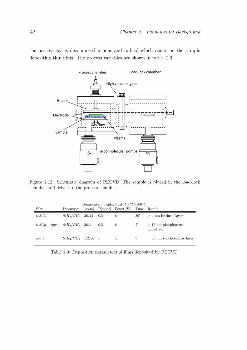
40 Chapter 2. Fundamental Background
the process gas is decomposed in ions and radical which reacts on the sample
depositing thin films. The process variables are shown in table 2.3.
High vacuum gate
Turbo molecular pumps
Process chamber Load-lock chamber
Sample
Plasma
Heater
Electrode
Gas flow
Figure 2.12: Schematic diagram of PECVD. The sample is placed in the load-lockchamber and driven to the process chamber
Temperature display/real (500oC/300oC)Film Precursors [sccm] P[mbar] Power [W] Time Result
a-SiCx SiH4/CH4 36/12 0.5 6 30" ∽ 4 nm Intrinsic layer
a-Si(n − type) SiH4/PH3 36/4 0.5 6 2’ ∽ 15 nm phosphorousdoped a-Si
a-SiCx SiH4/CH4 1.2/60 1 18 9’ ∽ 35 nm stoichiometric layer
Table 2.3: Deposition parameters of films deposited by PECVD.
2.4. Experimental techniques 41
2.4.4 Laser
During this thesis, laser processing has been used for locally doping p+ and n+
c-Si regions on IBC solar cells. The laser employed is a pulsed Nd-YAG lamp-
pumped working at 1064 nm in nanosecond regime in TEM00 mode (Starmark
SMP100 II Rofin-Baasel). Laser parameters such as power, pulse duration and
number of pulses, are varied in order to find the conditions leading to the optimal
electrical behavior of the formed junctions. The frequency is fixed to 4Khz and
two different laser pulse duration: 100 ns and 400 ns. Regarding the beam
characteristics, an objective lens with a focal length of 31.4 cm is used leading
to a beam waist radius of 70 µm with a Gaussian profile and a round shape. All
the experiments were performed at the same focal distance, as close as possible
to the beam focus. The energy of the laser beam can be adjusted by varying the
current intensity of the continuous lamp that pumps the Nd:YAG crystal. Power
measurements are realized just before every surface treatment with a Ophir power
meter F150 equipped with a thermal power sensor.
2.4.5 Characterization systems
Carrier lifetime measurement through photoconductance
technique
The effective lifetime of photogenerated carriers quantifies the recombination rate
occurring within a solar cell. Among them, non-contacting techniques are very
useful to examine the surface recombination at passivated surface of partially
processed samples, which are free of metal contacts. To generate the excess
carrier density and measure their effective lifetime, optical sources such as laser,
led arrays [56] or a simple flash-lamp [57] are used.
Photoconductance methods are based in the measurement of two parameters:
• Sample photoconductance, ∆σ
• The light intensity
In this thesis, the effective lifetime was measured using the photoconductance
tool WTC-120 commercialized by Sinton Consulting [57]. In this experimental
setup (See Fig. 2.13), the measured c-Si sample is illuminated by a Xenon flash
lamp generating the excess carriers within the sample which leads to an excess

42 Chapter 2. Fundamental Background
of conductance. The photoconductance, ∆σ, is measured contactless by using
inductive coupling. At the same time, the light intensity is measured through
a calibrated solar cell placed next to the measured sample. The excess carrier
density, ∆n, in the sample is calculated from ∆σ. The electron-holes photogene-
rated within the sample under measurement can be estimated, Gext(t). Reflection
losses of the sample are defined by an effective optical transmission factor, fopt,
to accurately determine Gext(t) from the light intensity that is monitored by the
reference solar cell. After determination both ∆n and Gext, τeff can be calculated
as a function of ∆n using the following equation [57]
τeff =∆n
Gext −d∆n
dt
(2.5)
Figure 2.13: Schematic and image of the carrier lifetime measurement system (WCT-120) used in this thesis
This method operates in quasi-steady-state (QSS-PC) and photoconductance
decay (PCD) regimes. The latter involves an abrupt pulse of illumination and
subsequent determination of the excess carrier density without illumination. A
very short flash (∼ 15 µs) creates an excess carriers which recombines depending
on recombination parameters of the bulk and surface. The advantage of this
method is that the only magnitude needed is the photoconductance of the sam-
ple since Gext = 0 (see equation 2.5). However relatively high τeff values are
also required to obtain reliable values. In QSS-PC regime the intensity of the
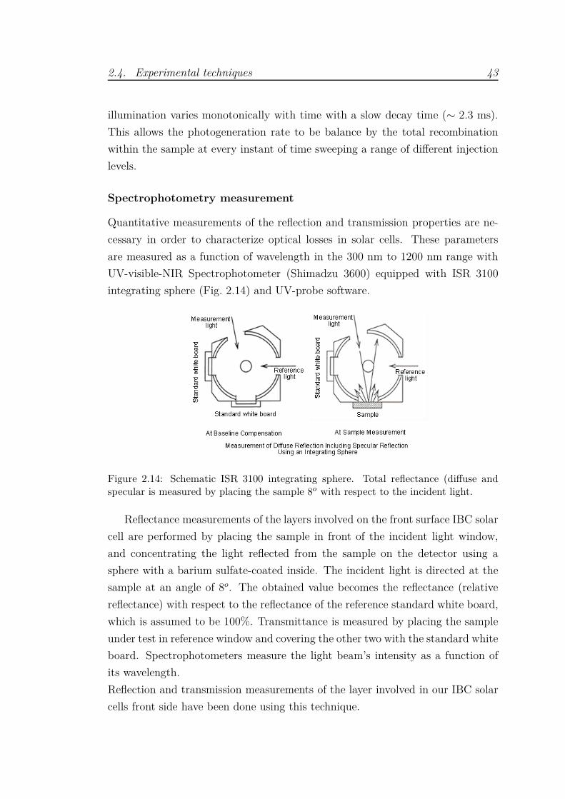
2.4. Experimental techniques 43
illumination varies monotonically with time with a slow decay time (∼ 2.3 ms).
This allows the photogeneration rate to be balance by the total recombination
within the sample at every instant of time sweeping a range of different injection
levels.
Spectrophotometry measurement
Quantitative measurements of the reflection and transmission properties are ne-
cessary in order to characterize optical losses in solar cells. These parameters
are measured as a function of wavelength in the 300 nm to 1200 nm range with
UV-visible-NIR Spectrophotometer (Shimadzu 3600) equipped with ISR 3100
integrating sphere (Fig. 2.14) and UV-probe software.
Figure 2.14: Schematic ISR 3100 integrating sphere. Total reflectance (diffuse andspecular is measured by placing the sample 8o with respect to the incident light.
Reflectance measurements of the layers involved on the front surface IBC solar
cell are performed by placing the sample in front of the incident light window,
and concentrating the light reflected from the sample on the detector using a
sphere with a barium sulfate-coated inside. The incident light is directed at the
sample at an angle of 8o. The obtained value becomes the reflectance (relative
reflectance) with respect to the reflectance of the reference standard white board,
which is assumed to be 100%. Transmittance is measured by placing the sample
under test in reference window and covering the other two with the standard white
board. Spectrophotometers measure the light beam’s intensity as a function of
its wavelength.
Reflection and transmission measurements of the layer involved in our IBC solar
cells front side have been done using this technique.
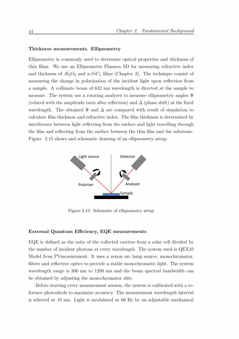
44 Chapter 2. Fundamental Background
Thickness measurements. Ellipsometry
Ellipsometry is commonly used to determine optical properties and thickness of
thin films. We use an Ellipsometer Plasmos SD for measuring refractive index
and thickness of Al2O3 and a-SiCx films (Chapter 3). The technique consist of
measuring the change in polarization of the incident light upon reflection from
a sample. A collimate beam of 632 nm wavelength is directed at the sample to
measure. The system use a rotating analyzer to measure ellipsometric angles Ψ
(related with the amplitude ratio after reflection) and ∆ (phase shift) at the fixed
wavelength. The obtained Ψ and ∆ are compared with result of simulation to
calculate film thickness and refractive index. The film thickness is determined by
interference between light reflecting from the surface and light travelling through
the film and reflecting from the surface between the thin film and the substrate.
Figure 2.15 shows and schematic drawing of an ellipsometry setup.
Light source
Polarizer Analyzer
Detector
Sample
Figure 2.15: Schematic of ellipsometry setup
External Quantum Efficiency, EQE measurements
EQE is defined as the ratio of the collected carriers from a solar cell divided by
the number of incident photons at every wavelength. The system used is QEX10
Model from PVmeasurement. It uses a xenon arc lamp source, monochromator,
filters and reflective optics to provide a stable monochromatic light. The system
wavelength range is 300 nm to 1200 nm and the beam spectral bandwidth can
be obtained by adjusting the monochromator slits.
Before starting every measurement session, the system is calibrated with a re-
ference photodiode to maximize accuracy. The measurement wavelength interval
is selected at 10 nm. Light is modulated at 66 Hz by an adjustable mechanical
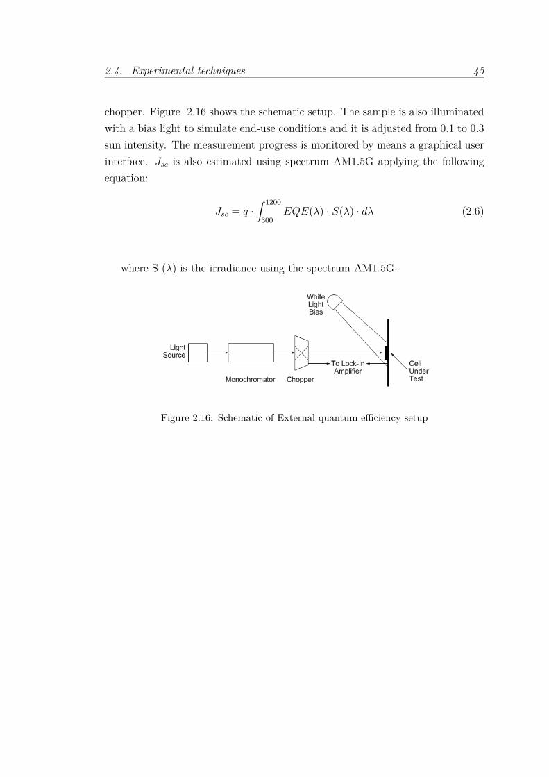
2.4. Experimental techniques 45
chopper. Figure 2.16 shows the schematic setup. The sample is also illuminated
with a bias light to simulate end-use conditions and it is adjusted from 0.1 to 0.3
sun intensity. The measurement progress is monitored by means a graphical user
interface. Jsc is also estimated using spectrum AM1.5G applying the following
equation:
Jsc = q ·
∫ 1200
300EQE(λ) · S(λ) · dλ (2.6)
where S (λ) is the irradiance using the spectrum AM1.5G.
Figure 2.16: Schematic of External quantum efficiency setup

46 Bibliography
Bibliography
[1] A. Richter, S.W. Glunz, F. Werner, J. Schmidt, and A. Cuevas. Improved
quantitative description of auger recombination in crystalline silicon. Physi-
cal Review B: Condens. Matter Mater. Physc., 86:165202, 2012.
[2] M. Labrune. Silicon surface passivation and epitaxial growth on c-Si by low
temperature plasma processes for high efficiency solar cells. PhD thesis, Ecole
Polytechnique, 2011.
[3] C. Battaglia, A. Cuevas, and S. De Wolf. High-efficiency crystalline siliocn
solar cells: status and perspectives. Energy and Environmental Science, 9:
1552–1576, 2016.
[4] T. Tiedje, E. Yablonovitch, G.D. Cody, and B.G. Brooks. Limiting efficiency
of silicon solar cells. IEEE Transactations on Electron Devices, 5:711–716,
1984.
[5] R. Brendel. Thin-Film Crystalline Silicon Solar Cells: Physics and Techno-
logy. 2011.
[6] M.J. Kerr. Surface, emitter and bulk recombination in silicon and deve-
lopment of silicon nitride passivated solar cells. PhD thesis, 2002. URL
https://digitalcollections.anu.edu.au/handle/1885/47459.
[7] J. Zhao, A. Wang, and MA. Green. 24.5% efficiency PERT silicon solar cells
on SEH MCZ substrates and cell performance on other SEH CZ and FZ
substrates. Solar Energy Materials and Solar Cells, 66:27–36, 2001.
[8] R.J. Schwartz. Silicon solar cells for high concentration applications. In
IEEE International Electron Devices Meeting, Washington D.C, pages 350–
352. IEEE, 1975.
[9] M. Green, K. Emery, Y. Hishikawa, W. Warta, and E. Dunlop. Solar cell
efficiency tables (version 47). Progress in Photovoltaics: Research and Appli-
cations, 24:3–11, 2015.
[10] M. Green, K. Emery, Y. Hishikawa, W. Warta, and E. Dunlop. Solar cell
efficiency tables (version 43). Progress in Photovoltaics: Research and Appli-
cations, 22:1–9, 2014.

Bibliography 47
[11] E. Van Kerschaver, R. Einhaus, J. Szlufcik, J. Nijs, and R. Mertens. A novel
silicon solar cell structure with both external polarity contacts on the back
surface. In 2nd World Conference Photovoltaic Energy Convers, Vienna,
(Austria), pages 1479–1482, 1998.
[12] E. Lohmuller, M. Thanasa, B. Thaidigsmann, and F. Clement. Electrical
properties of the rear contact structure of MWT silicon solar cells. Solar
Energy Materials and Sola cells, 137:293–302, 2015.
[13] E. Lohmuller, B. Thaidigsmann, M. Pospischil, U. Jager, S. Mack, J. Specht,
J. Nekarda, M. Retzlaff, A. Krieg, F. Clement, A. Wolf, D. Biro, and R. Preu.
20% efficient passivated large-area metal wrap through solar cells on boron-
doped cz silicon. IEEE Electron Device Letters, 32:1719–1721, 2011.
[14] T. Benjamin, L. Michael, W. Andreas, C. Florian, B. Daniel, and P. Ralf.
The path to industrial production of highly efficient metal wrap through
silicon solar cells. GREEN, 2:171–6, 2012.
[15] W. Yin, X. Wang, F. Zhang, and L. Zhang. 19.6% cast mono-mwt solar cells
and 268 w modules. In 38th Photovoltaic Specialists Conference (PVSC),
pages 1–5. IEEE, 2012.
[16] M. W. P. E. Lamers, C. Tjengdrawira, M. Koppes, I. J. Bennett, E. E.
Bende, T. P. Visser, E. Kossen, B. Brockholz, A. A. Mewe, I. G. Romijn,
E. Sauar, L. Carnel, S. Julsrud, T. Naas, P. C. de Jong, and A. W. Weeber.
17.9% metal-wrap-through mc-si cells resulting in module efficiency of 17.0%.
Progress in Photovoltaics: Research and Applications, 20:62–73, 2012.
[17] M.K. Mat Desa, S. Sapeaia, Sopiana K. Azharia, A.W., M.Y. Sulaimana,
N. Amina, and S.H. Zaidia. Silicon back contact solar cell configuration:
A pathway towards higher efficiency. Renewable and Sustainable Energy
Reviews, 60:1516–1532, 2016.
[18] O. Nichiporuk, A. Kaminski, J. Kraiem, S. Quoizola, A. Fave, and M. Lemiti.
Realisation of interdigitated back contacts solar cells on thin epitaxially
grown silicon layers on porous silicon. In 19th Photovoltaic Specialists Con-
ference (PVSC), pages 1127–1130. IEEE, 2004.
48 Bibliography
[19] R. Kühn, A. Boueke, M. Wibral, C. Zechner, P. Fath, G. Willeke, and
E. Buchner. Investigation of the effect of p/n-junctions bordering on the
surface of silicon solar cells. In 2nd WCPSEC, Vienna, pages 1390–1393,
1998.
[20] A. Schonecker, A.W. Weeber, W.C. Sinke, C. Zechner, Kress A., and P Fath.
Attacking limiting factors in 10 x 10 cm2 multicristalline silicon, emitter
wrap-through solar cell design and processing. In 2nd WCPSEC, Vienna,
pages 1677–1680, 1998.
[21] D.D. Smith and J.M. Gee. Review of back-contact silicon solar cells for low
cost application. In 16th EPVSC, Glassgow, pages 1104–1107, 2000.
[22] R.M. Swanson, S.K. Beckwith, R.A. Crane, W.D. Eades, Y.H. Kwark, R.A.
Sinton, and S.E. Swirhun. Point contact silicon solar cells. IEEE, Transaction
on Electron Devices, 32(5):661–664, 1982.
[23] R.M. Swanson. Point contact silicon solar cells. In 17th IEEE PVSEC, pages
1294–1296, 1984.
[24] G. Stehelin, J.P David, F. Floret, and P. Verlinden. Comparison of the
open-circuit voltage for point contact and linear contact ibc solar cells. In
7th EPVSC, Sevilla, pages 865–869, 1986.
[25] P. Verlinden, F. Van De Wiele, G. Stehelin, F. Floret, and J.P David. High ef-
ficiency interdigitated back contact silicon solar cells. In 19th IEEE PVSEC,
New Orleans, pages 405–410. IEEE, 1987.
[26] D. Carrió, P. Ortega, I. Martín, G. López, J. M. López-González, A. Orpella,
C. Voz, and R. Alcubilla. Rear Contact Pattern Optimization based on 3D
Simulations for IBC Solar Cells with Point-like Doped Contacts. Energy
Procedia, 55:47–52, 2014.
[27] J. M. López-González, I. Martín, P. Ortega, A. Orpella, and R. Alcubilla.
Numerical simulations of rear point-contacted solar cells on 2.2 ohm.cm p-
type c-si substrates. Progress in Photovoltaics: Research and Applications,
23:69–77, 2013.
Bibliography 49
[28] R.A. Sinton and R.M. Swanson. Design criteria for si point-contact concen-
trator solar cells. IEEE, Transaction on Electron Devices, 34(10):2116–2123,
1987.
[29] P. Verlinden, F. Van de Wiele, G. Stehelin, and J.P. David. An interdigi-
tated back contact solar cell with high efficiency under concentrated sunlight.
In 18th IEEE Photovoltaic Specialists Conference, Las Vegas, pages 55–60,
1985.
[30] R.R. King, R.A. Sinton, and Swanson R.M. Front and back surface fields for
point-contact solar cells. In 20th IEEE Photovoltaic Specialist Conference
PVSEC, Las Vegas, pages 538–544. IEEE, 1988.
[31] P. Verlinden, R.A. Sinton, and R.A. Swanson. High efficiency large area back
contact concentrator solar cells with a multilevel interconnection. Interna-
tional Journal of Solar Energy, 6(6):347–366, 1988.
[32] R.A. Sinton and R.M. Swanson. Simplified backside-contact solar cells.
IEEE, Transaction on Electron Devices, 37(2):348–352, 1990.
[33] R.A. Sinton, P. Verlinden, D.E. Kane, and R.M. Swanson. Development
efforts in silicon backside-contact solar cells. In 8th European Photovoltaic
Solar Energy Conference, EU-PVSEC, Florence, pages 1472–1476, 1988.
[34] P.J. Verlinden, R.A. Sinton, K. Wickham, R.A. Crane, and R.M. Swanson.
Backside-contact silicon solar cells with improved efficiency for the ’96 world
solar challenge. In 14th European Photovoltaic Solar Energy Conference,
EU-PVSEC, Barcelona, pages 96–99, 1997.
[35] W.P. Mulligan, D.H. Rose, M.J. Cudzinovic, D.M. De Ceuster, K.R. McIn-
tosh, D.D. Smith, and R.M. Swanson. Manufacture of solar cells with 21%
efficiency. In 19th European Photovoltaic Solar Energy Conference, EU-
PVSEC, Paris, pages 387–390, 2004.
[36] D. De Ceuster, P. Cousins, D. Rose, D. Vicente, P. Tipones, and W. Mul-
ligan. Low cost, high volume production of > 22% efficiency silicon solar
cells. In 22nd European Photovoltaic Solar Energy Conference, EU-PVSEC,
Milan, pages 816–819, 2007.

50 Bibliography
[37] J. Dicker, J.O. Schumacher, W. Warta, and S.W. Glunz. Analysis of one-sun
monocrystalline rear-contacted silicon solar cells with efficiencies of 22.1%.
Journal of Applied Physics, 91(7):4335–4343, 2002.
[38] J.H. Guo, B.S. Tjahjono, and J.E. Cotter. 19.2% efficiency n-type laser-
grooved silicon solar cells. In 31sth IEEE Photovoltaic Specialist Conference
PVSEC, Orlando, pages 983–986. IEEE, 2005.
[39] P. Engelhart, N.P. Harder, R. Grischke, A. Merkle, R. Meyer, and R. Bren-
del. Laser structuring for back junction silicon solar cells. Progress in Pho-
tovoltaics: Research and Application, 15:237–243, 2006.
[40] J. Zhao, A. Wang, M.A. Green, and F. Ferrazza. Novel 19.8% efficient
"honeycomb "textured multicrystalline and 24.2% monocrystalline silicon so-
lar cells. Applied Physics Letters, 73:1991–1993, 1998.
[41] K. Masuko, M. Shigematsu, T. Hashiguchi, D. Fujishima, M. Kai,
N. Yoshimura, and T. et al. Yamaguchi. Achievement of more than 25%
conversion efficiency with crystalline silicon heterojunction solar cell. IEEE
journal of photovoltaics, 4(6):1433–1435, 2014.
[42] J Nakamura, N. Asano, T Hieda, C. Okamoto, H. Katayama, and K. Naka-
mura. Development of heterojunction back contact si solar cells. IEEE
journal of photovoltaics, 4(6):1491–1495, 2014.
[43] D. Smith, P. Cousins, S. Westerberg, R. De Jesus-Tabajonda, G. Aniero, and
Y-C. Shen. Toward the practical limits of silicon solar cells. IEEE journal
of photovoltaics, 4(6):1465–1469, 2014.
[44] E. Franklin, K. Fong, K. McIntosh, A. Fell, A. Blakers, T. Kho, D. Walter,
and D. et al. Wang. Design, fabricationand charactisation of a 24.4% efficient
interdigitated back contact solar cell. Progress in Photovoltaics: Research
and applications, DOI 10.1002 pip.2556, 2014.
[45] K.S. Ji, J. Syn, H.and Choi, H.M. Lee, and D. Tech. Digest Kim. In 21st
International Photovoltaic Science and Engineering Conference, Fukuoka,
Japan, pages 3A–1O–06, 2011.

Bibliography 51
[46] P. Ortega, I. Martín, G. Lopez, M. Colina, A. Orpella, C. Voz, and R. Alcu-
billa. p-type c-Si solar cells based on rear side laser processing of Al2O3/SiCx
stacks. Solar Energy Materials and Solar Cells, 106:80–83, 2012.
[47] H. Savin, P. , Repo, G. von Gastrow, P. Ortega, E. Calle, M. Garín,
and R. Alcubilla. Black silicon solar cells with interdigitated back-contacts
achieve 22.1% efficiency. Nature Nanotechnology, 10:624–628, 2015.
[48] G. Masmitja, P. Ortega, I. Martín, G. López, and R. Voz, C.and Alcubilla.
IBC c-Si(n) Solar Cells Based on Laser Doping Processing for Selective Emit-
ter and Base Contact Formation. Energy Procedia, 92:956–961, 2016.
[49] G. López, G. Ortega, i: Marín, C. Voz, A. Orpella, and R. Alcubilla. "Cold"
process for IBC c-Si solar cells fabrication. Energy Procedia, 92:652–660,
2016.
[50] R.A. Sinton, Y. Kwark, and R.M. Gan, J.Y. abd Swanson. 27.5 percent
silicon concentration solar cells. IEEE Electron Devices Letter, EDL-7:567–
569, 1986.
[51] R.R. King, R.A. Sinton, and R.M. Swanson. One-sun, single-crystalline
silicon solar cell research. Technical Report, Solid-State Electronics Lab.,
1991.
[52] A Mohr. Silicon concentrator cells in a two-stage photovoltaic system with a
concentration factor of 300X. PhD thesis, Universiät Freiburg, 2005.
[53] M. Dahlinger, B. Bazer-Bachi, Köhler J.R. Röder, T.C. and, R. Zapf-
Gottwick, and J.H Werner. 22.0% Efficient laser doped back contact solar
cells. Energy Procedia, 38:250–253, 2013.
[54] W. Kern and D. Puotinen. Cleaning solutions based on hydrogen peroxide
for use in silicon semiconductor technology. RCA review, 31:187–206, 1970.
[55] K McIntosh and Luke P. Recombination at textured silicon surfaces passi-
vated with silicon dioxide. Journal of Applied Physics, 105:124520, 2009.
[56] J. Schmidt and Armin G. Aberle. Accurate method for the determination of
bulk minority-carrier lifetimes of mono- and multicrystalline silicon wafers.
Journal of Applied Physics, 81:6186, 1997.

52 Bibliography
[57] Ronald A. Sinton and A. Cuevas. Contactless determination of current-
voltage characteristics and minority-carrier lifetimes in semiconductors from
quasi-steady-state photoconductance data. Applied Physics Letters, 69:2510,
1996.
Chapter 3
c-Si surface passivation by Al2O3
thin films
The improvement of the electrical quality of the c-Si surface is crucial
in the development of high efficiency c-Si solar cells. This chapter in-
troduces fundamental recombination mechanisms in c-Si and the con-
ventional surface passivating films used in solar cells fabrication. The
second part is focused on the study and optimization of Al2O3 film
deposited by thermal-ALD used as passivating c-Si surface. The ex-
perimental is carried out depositing Al2O3 and Al2O3/a−SiCx stacks
at different conditions on both random textured and polished surfaces.
Optical properties are also measured and analyzed
3.1 Introduction
Generation in semiconductors is the process whereby electron-hole pairs are crea-
ted. The implied energy comes from thermal activity, electrical excitation, or
through the absorption of photons, as occurs in solar cells. Recombination is the
opposite effect in which an electron from the conduction band is combined with a
hole from the valence band and consequently a electron-hole pair is annihilated.
This process liberates energy in form of photons or phonons. Recombination rate,
U, quantifies this process and its minimization is crucial in high efficiency solar
cell development. As the recombination rate decreases, the photo generated ca-
rries increase their contribution to the photo-current and therefore the conversion
efficiency of the solar cell also increases.
53
54 Chapter 3. c-Si surface passivation by Al2O3 thin films
Experimentally, the recombination rate can not be directly measured and instead
it is used the recombination lifetime (τ) defined as the average time of a carrier
between its generation and its recombination. This term is applied when the
solar cell works under mid-injection or even high-injection conditions. Under
low-injection conditions recombination lifetimes are referred to minority carriers
and the term used is minority carrier lifetimes. In this thesis lifetime is studied
for a wide range of injection conditions and we always use the term recombination
lifetime to refer any carrier lifetime.
The relationship between recombination rate and lifetime is given by:
U =∆n
τ(3.1)
where ∆n is the excess minority carrier density per unit volume and ∆n = n−n0
(n0 is the minority carrier density under thermal equilibrium)1.
3.2 Recombination in the bulk of c-Si
Under thermal equilibrium and at temperatures higher than absolute zero the
recombination and thermal generation are equal and consequently the excess ca-
rrier density is zero. In the case of solar cells we are interested in study the device
exposed to an external source of light. Assuming a constant light intensity and
steady-state conditions, an excess carrier density is present in the semiconductor
and for every recombination process a net recombination rate (U) can be defined
as (3.1)
Three fundamental recombination mechanisms occur in the bulk of crystalline
silicon (c-Si):
• Radiative recombination
• Auger recombination, and
1∆n can be referred to both electron or hole excess carrier density, since we assumed ∆n ∼=∆p in quasi-neutral regions
3.2. Recombination in the bulk of c-Si 55
• Recombination through defects in the bandgap, or Shockley-Read-Hall re-
combination
Radiative and Auger recombination are semiconductor intrinsic processes and
therefore, unavoidable. Shockley-Read-Hall recombination (SRH) is an extrinsic
recombination via defect states and hence it can significantly be reduced by im-
proving the material quality. The use of high quality thin substrates considerably
minimizes the recombination processes into the bulk. Therefore, the recombina-
tion at the silicon surface becomes dominant and the reduction of such surface
recombination is a requirement for high efficiency solar cells development.
The total recombination rate within the bulk is defined as the sum of each re-
combination mechanisms:
U = URad + UAug + USRH =∆n
τRad
+∆n
τAug
+∆n
τSRH
=∆n
τbulk
(3.2)
The corresponding recombination lifetime can be calculated as:
1τbulk
=1
τRad
+1
τAug
+1
τSRH
(3.3)
3.2.1 Radiative recombination
Radiative or band to band recombination (Urad) is the direct annihilation of an
electron from the conduction band and a hole from valence band releasing the ex-
cess energy (energy close to that of the bandgap) as a photon [1], as schematically
depicted in Fig. 3.1. This recombination mechanism in c-Si is a process with
relative low probability due to the indirect band gap of c-Si and it is normally of
minor importance for solar cells made with this material [2].
This recombination mechanism is dominant in direct bandgap semiconductor
(e.g.,CdTe y GaAs) and depends on the density of electrons and holes, since one
of each is needed in this process. The net recombination rate can be expressed
by:

56 Chapter 3. c-Si surface passivation by Al2O3 thin films
Urad =∆n
τrad= B∆n(Ndop + ∆n) (3.4)
where Ndop is the corresponding doping density (acceptor or donor) and B is the
recombination radiative coefficient.
Accordingly to 3.1, τrad is defined as follow:
τrad =1
B(Ndop + ∆n)(3.5)
Ec
Ev
_
+
Photon and/or
phonons
Figure 3.1: Radiative recombination in a semiconductor
In silicon, many authors have reported on the determination of this coefficient.
At room temperature, Michaelis and Pilkuhn determined a B = 1.7×10⁻¹⁵cm3s−1
[3], Ruff et al. a B = 7 × 10⁻¹⁵cm3s−1 [4] and Schlangenotto et al. a B =
0.95 × 10⁻¹⁴cm3s−1 [5]. More recently a complete study comes from the work
done by T. Trupke et al.[6]. This paper include a discussion about the previous
research and determined B = 4.73 × 10⁻¹⁵cm3s−1
3.2.2 Auger recombination
Auger recombination is a three-particle interaction where an electron from con-
duction band recombines with a hole from valence band. The energy and mo-
mentum conservation are assured by a third particle (electron in the conduction
band or hole in the valence band)[7], as it is shown in Fig. 3.2. The total Auger
recombination UAuger is given by:
UAuger = Cn(n2p − n20p0) + Cp(np2 − n0p
20) (3.6)
where n(p) is the electron (hole) density, n0(p0) the electron (hole) density at
equilibrium and Cn, Cp are Auger coefficients.
Many works concerning the determination of these coefficients can be found
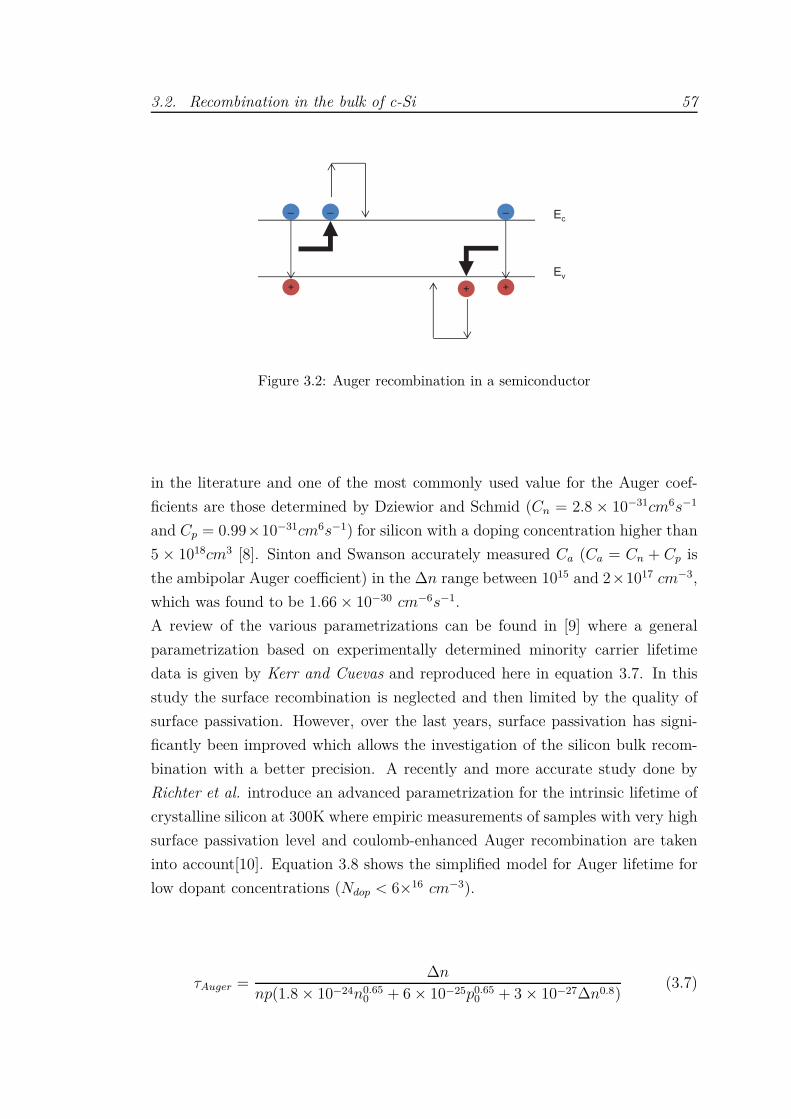
3.2. Recombination in the bulk of c-Si 57
Figure 3.2: Auger recombination in a semiconductor
in the literature and one of the most commonly used value for the Auger coef-
ficients are those determined by Dziewior and Schmid (Cn = 2.8 × 10⁻³¹cm6s−1
and Cp = 0.99×10⁻³¹cm6s−1) for silicon with a doping concentration higher than
5 × 1018cm3 [8]. Sinton and Swanson accurately measured Ca (Ca = Cn + Cp is
the ambipolar Auger coefficient) in the ∆n range between 1015 and 2×1017 cm−3,
which was found to be 1.66 × 10⁻³⁰ cm−6s−1.
A review of the various parametrizations can be found in [9] where a general
parametrization based on experimentally determined minority carrier lifetime
data is given by Kerr and Cuevas and reproduced here in equation 3.7. In this
study the surface recombination is neglected and then limited by the quality of
surface passivation. However, over the last years, surface passivation has signi-
ficantly been improved which allows the investigation of the silicon bulk recom-
bination with a better precision. A recently and more accurate study done by
Richter et al. introduce an advanced parametrization for the intrinsic lifetime of
crystalline silicon at 300K where empiric measurements of samples with very high
surface passivation level and coulomb-enhanced Auger recombination are taken
into account[10]. Equation 3.8 shows the simplified model for Auger lifetime for
low dopant concentrations (Ndop < 6×16 cm−3).
τAuger =∆n
np(1.8 × 10⁻²⁴n0.650 + 6 × 10⁻²⁵p0.65
0 + 3 × 10⁻²⁷∆n0.8)(3.7)
58 Chapter 3. c-Si surface passivation by Al2O3 thin films
τAuger =∆n
np(8.7 × 10⁻²⁹ + n0.910 + 6 × 10⁻³⁰p0.94
0 + 3 × 10⁻²⁹∆n0.92)(3.8)
Auger recombination is typically the dominant intrinsic bulk recombination mech-
anism in solar cells. Both intrinsic recombinations (Auger and radiative) are de-
pendent on the c-Si doping level and charge carrier density [9].
3.2.3 Recombination through defects in the bandgap
, SRH
The presence of defects within the silicon crystal due to impurities or crystal-
lographic imperfections creates a number of states within the bandgap. These
defect levels act as carrier traps for free electrons or holes and greatly facilitate
recombination through a two-step process resulting in the dominant mechanism
in indirect bandgap semiconductors. The recombination happens when an elec-
tron from conduction band (or a hole from valence band) is trapped firstly at this
defect level and then released to the valence band (or conduction band). There
are four interactions between the defect center and the charge carrier as it can
be seen in figure 3.3:
• 1. Capture of an electron from conduction band
• 2. Emission of an electron from defect level to conduction band
• 3. Capture of a hole from valence band
• 4. Emission of a hole from defect level to valence band
Carrier recombination does not happen when the charge carrier is released
into the same band where it was captured. That is, when the electron is released
to conduction band (step 1 and 2) or the hole is released to valence band (step 3
and 4).
Recombination through defects is an extrinsic process and was described by
Shockley and Read [1] and Hall [11] in 1952. SRH recombination rate USRH , for
a single defect level is described by the following equation:
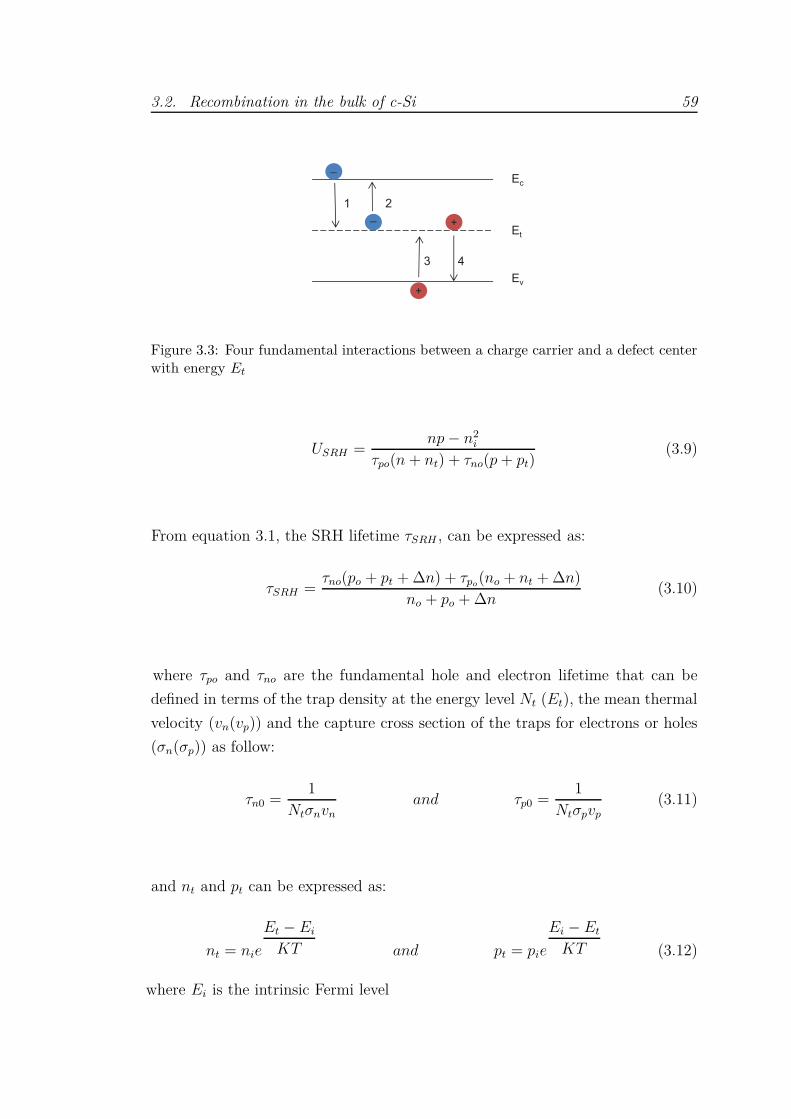
3.2. Recombination in the bulk of c-Si 59
Figure 2.1 a,b,c
Figure 3.3: Four fundamental interactions between a charge carrier and a defect centerwith energy Et
USRH =np − n2
i
τpo(n + nt) + τno(p + pt)(3.9)
From equation 3.1, the SRH lifetime τSRH , can be expressed as:
τSRH =τno(po + pt + ∆n) + τpo
(no + nt + ∆n)no + po + ∆n
(3.10)
where τpo and τno are the fundamental hole and electron lifetime that can be
defined in terms of the trap density at the energy level Nt (Et), the mean thermal
velocity (vn(vp)) and the capture cross section of the traps for electrons or holes
(σn(σp)) as follow:
τn0 =1
Ntσnvnand τp0 =
1Ntσpvp
(3.11)
and nt and pt can be expressed as:
nt = nie
Et − Ei
KT and pt = pie
Ei − Et
KT (3.12)
where Ei is the intrinsic Fermi level
60 Chapter 3. c-Si surface passivation by Al2O3 thin films
We must underline that when the defect is close to Ei level, i.e. close to the
midgap, the SRH recombination will be the highest one. Contrariwise, if the de-
fect energy is located close to conduction or valence band (shallow defects), the
defect will act more like a trap for electrons or holes rather like a recombination
center. These shallow defects become more active at high-injection level.
Finally, all these recombination processes lead to a total effective bulk lifetime
previously described at the equation 3.3.
Figure 3.4, shows the Auger, radiative and SRH recombination lifetime as
a function of the excess carrier density, ∆n (injection level) for 2.5 Ωcm n- and
p-type substrates used in this thesis (a and b respectively) corresponding to a
donor density of 1.88 ×1015 cm−3 and a acceptor density of 5.7 ×1015 cm−3. The
resulting τbulk is also shown is black line. To calculate τrad and τAuger equation 3.5
the constant value B = 4.73 × 10⁻¹⁵ cm3s−1 and 3.8 have been used. In the case
of τSRH , we consider one defect located in the middle of the bandgap (Et = Ei)
and τn0 = τp0 = 2.5 ms [12]. The radiative lifetime is constant at low injection,
but then decreases and continues decreasing as the injection level increases. At
high injection depends on the inverse of the carrier density (τrad ∝ 1∆n
). Auger
lifetime depends on the inverse of the carrier density squared (τAuger ∝ 1∆n2 ) and
hence it shows a stepper slope with the injection level than τrad. In fact, Auger
recombination is dominant in highly doped c-Si, e.g. in emitters) and under light
concentration.

3.3. Recombination at c-Si surface 61
Lif
etim
e (µ
s)
Excess carrier density (cm-3)
Rad
Auger
SRH
Bulk
(a) n-type c-Si substrate
Lif
etim
e (µ
s)
Excess carrier density (cm-3)
(b) p-type c-Si substrate
Figure 3.4: Fundamental recombination mechanism in the bulk of a n-type and p-type c-Si substrate at 300 K (ni = 9.65 · 109 cm−3, ρp−type = ρn−type = 2.5 Ωcm,τn0 = τp0 = 2.5ms)
3.3 Recombination at c-Si surface
The continuity of the crystal lattice is completely lost at the surface of any crys-
talline material [13]. The large number of partially bonded silicon atoms gives
rise to many dangling bonds and therefore, a high amount of defect states are
present within the bandgap leading to a high recombination rate. Recombination
at c-Si surface can be described similar as bulk SRH recombination by replacing
the bulk carrier density by the surface carrier density. The net recombination
rate per unit area, can be defined as follow:
Us =nsps − n2
i
ns + n1
Spo+
ps + p1
Sno
(3.13)
where ns and ps are the concentrations of electrons and holes at the surface
(ns = ∆ns + no, ps = ∆ns + po), and Spo and Spo are related to the density
of surface states per unit area, Nst, the capture cross-sections, σp and σn and
thermal velocity, vth for the specific defect as follow:
Sno ≡ σnvthNst and Spo ≡ σpvthNst (3.14)
62 Chapter 3. c-Si surface passivation by Al2O3 thin films
Equation 3.13 shows that surface recombination depends on the properties of
the surface states, on the injection level and on the doping density. The energy
level of the defects dependence is the same to the Shockley-Read-Hall lifetime.
Surface recombination can be characterized by the surface recombination velocity
in cm/s, S, as:
Us = S∆ns (3.15)
where ∆ns is the minority carrier density at the surface. An electric field is
usually found at c-Si surface and ∆ns could be far away from ∆ps since the
electric field creates large differences between ns and ps [14]. Hence, an effective
surface recombination velocity, Seff , is defined as:
Us = Seff .∆n (3.16)
where ∆n ∼= ∆p is the minority carrier density at the quasi-neutral bulk region
and easily measured by changing the illumination level.
The surface recombination is the dominant recombination mechanism in sili-
con and the reduction of such parameter, i.e. surface passivation, is of paramount
importance to maintain the minority carrier high and achieve high efficiency solar
cells.
There are two fundamental passivation mechanisms:
• Reducing the density of the interface states
• Modifying the relative concentration of photogenerated electrons and holes
near the surface.
Saturation of defects
The high amount of defects at the surface can be reduced by saturating the
remaining silicon dangling bonds. This strategy represents the direct reduction
of Sno and Spo described by equation (3.13). By depositing or growing an appro-
priate dielectric layer over the c-Si surface, Dit(E)2 is decreased and consequently
2Instead of Nst. Dit(E) defines a density of states as function of energy level. There isa large number of levels within the bandgap, each of them with a determinated density andcapture cross-section
3.4. The Effective lifetime of c-Si 63
Us. This strategy is more sensitive to the presence of defects at the silicon surface
than the field effect passivation.
Modification of the photogenerated carriers
When the population of the two types of carriers (electrons and holes) is equal,
the recombination rate at the surface is maximum. This strategy consists of re-
ducing one type of carriers at the interface by shielding the action of one type
of carriers and therefore strongly reduce the recombination rate. This can be
achieved by doping the semiconductor surface to repel the minority carriers such
as in an emitter region or a back-surface-field (BSF). Another strategy consists in
depositing or growing a charged film which also repels one type of carriers, elec-
trons or holes depending on the type of fixed charge in the overlying dielectric
film.
The films employed in solar cells for passivating the c-Si surface use a combina-
tion of both passivating strategies and usually is achieved by dielectric material
(SiO2, SiNx, SiCx, Al2O3) or semiconductor such a a-Si:H.
3.4 The Effective lifetime of c-Si
The total losses in the c-Si bulk and at the c-Si surface results in the so-called
effective lifetime of the minority charge carriers (τeff) and can be experimentally
measured. In general, the recombination processes can be considered to occur
independently and the total recombination is the sum of the individual recombi-
nation mechanisms and therefore:
1τeff
=1
τbulk+
1τsurface
(3.17)
where the first term correspond to:
1τbulk
=1
τrad
+1
τAuger
+1
τSRH
=1
τint
+1
τSRH
(3.18)
where τint is the intrinsic recombination parameter combining both Auger and
radiative mechanisms.
A c-Si sample symmetrically passivated with identical dielectric film the τeff

64 Chapter 3. c-Si surface passivation by Al2O3 thin films
can be written as:
1τeff
=1
τbulk
+2Seff
W(3.19)
where W is the c-Si sample thickness.
In all the experiments performed in this thesis Float Zone silicon wafers of very
high quality are employed. Therefore, the presence of defects within the bulk is
extremely low and the corresponding SRH lifetime will be assumed to be infinite.
Consequently, expression 3.19 can be simplified as follow:
1τeff
=1
τint
+2Seff
W(3.20)
From this expression, we can extract the maximum surface recombination
(Seff,max) assuming the bulk lifetime as infinite.
Seff,max =W
2 × τeff(3.21)
Equation 3.21 will be the expression used in this thesis and it results from the
effective lifetime measurements using the photoconductance technique explained
in section 2.4.5.
3.5 State-of-the-art of c-Si surface passivation
In the 1980s an intense research and development in the field of passivation layers
was carried out due to the successful implementation of passivating layers for
high-efficiency devices (higher than 20%). According to their main passivation
mechanism these layers can be divided into three groups:
• Thermally grown silicon dioxide (SiO2)
• Amorphous silicon based compounds: Amorphous hydrogenated silicon ni-
tride (a-SiNx:H), silicon carbide(a-SiCx:H) and intrinsic amorphous silicon
(i a-Si:H)
• Aluminum oxide (Al2O3)
3.5. State-of-the-art of c-Si surface passivation 65
3.5.1 Thermally grown silicon dioxide, SiO2
It is the state-of-the-art surface passivation layer on lightly doped n- and p-type
c-Si. It was the passivation layer employed for the first solar cells with efficien-
cies higher than 20%. On highly doped n-type c-Si (e.g. n+ emitter) the level
of surface passivation results excellent [15]. However, the passivation quality of
p-type emitters is poorer [14].
The excellent surface passivation achieved with this film is mainly attributed
to high quality of the c-Si/SiO2 interface that reduces the density of states at
the interface (∼ 109cm−2eV −1). In addition, positive charge densities within the
dielectric layer (up to 1011cm−2) [2],[16] cause a weak field effect passivation [17]
and contribute to lead to Seff values as low as 2 cm/s (substrate n-type) and 12
cm/s (p-type) [18]. Due to the positive sign of these charges, electron are drifted
to the c-Si surface and holes are rejected. As a consequence, at the surface of low
resistivity p-type c-Si and p-type emitters, electron density equals hole density
resulting in an increasing in surface recombination.
The high quality interface is due to the fact that thermal SiO2 is grown onto
the silicon wafer by oxidation at elevated temperatures (1000-1100 C) guaran-
teeing an unaffected final interface by initial c-Si surface conditions. A post-
deposition anneal in H2 atmosphere further improves the electrical passivation
by supplying H to the interface. Another method is the deposition of a sac-
rificial/structural Al film in the SiO2 followed by a anneal process at 400 C
typically. This so-called Alneal generates atomic hydrogen, which effectively re-
duces the Si/SiO2 interface states density [14].
The high growth temperatures employed are the main limitation for the appli-
cation thermal SiO2 as passivating layer requiring high purity c-Si to avoid sig-
nificant bulk time degradation [19]. Moreover, the high temperature is a clear
disadvantage from production cost and throughput point of view. On the other
hand, the SiO2 refractive index (1.47) is rather low to be applied as single an-
tireflection coating on the front side of c-Si solar cells.
66 Chapter 3. c-Si surface passivation by Al2O3 thin films
3.5.2 Amorphous silicon-based compounds
Between such compounds we can find amorphous silicon (a-Si), silicon nitride
(a-SiNx), silicon carbide (a-SiCx). Deposition conditions of these layer strongly
affects the optical and electronic properties. High content of silicon presents
strong optical absorption in visible-ultraviolet range and when the content of Si
is low, light absorption and conductivity decrease, thus exhibiting transparency
and very good dielectric properties.
Methods based on decomposition of hydrogenated gases are usually used ensuring
a high content of hydrogen that improves the surface passivation by saturating
dangling bonds. Plasma excitation systems are the most widespread methods.
Amorphous silicon nitride, a − SiNx : H
Extensive research has been led during last decades to produce silicon nitride
with excellent surface passivation properties. The positive fixed charge density is
particularly beneficial in the passivation of n-type c-Si as the minority carriers (i.e.
holes) are effectively shielded from c-Si surface and wherein an accumulation of
majority carriers takes place. A substantial problem of a-SiNx passivation layers
with their high built-in positive charge is that they yield inversion layers for low-
doped p-type c-Si which can lead to a parasitic shunting between contacts [20].
Seff as low as 6 cm/s and 22 cm/s have been reported on 1.5 Ωcm n-type and 1
Ωcm p-type passivated by a-SiNx:H, respectively [21].
In order to reduce this shunting effect, some authors suggest the use of a
thin SiO2 layer between Si and SiNx [22]. Thermally grown SiO2/SiNx stacks
provide a high level of passivation due to a low interface density [23],[24]. The
combination of such stacked films on p-type, 1 Ωcm wafers resulted in Seff values
lower than 3 cm/s. More recently, low-temperature SiOx/a-SiNx synthesized
by plasma enhanced chemical vapor deposition (PECVD) has demonstrated a
good alternative to thermal oxidation and very low Seff has been obtained (i.e. 6
cm/s and 11 cm/s for n- and p-type c-Si on 3.5 Ωcm and 2.2 Ωcm respectively)[25].
Apart from its excellent passivation properties, silicon nitride shows two more
advantages:
• Its refractive index can be widely tuned in the range of 1.9 to 2.3 controlled
by the quantity of Si within the layer. More quantity of Si involves higher
3.5. State-of-the-art of c-Si surface passivation 67
refractive index. The available range allows to use SiNx as optimum anti-
reflection coating (ARC) with n = 1.9 [26]. Schmidt et al. showed that films
with a refractive index equal to 2.1 enhanced the effective lifetime after a
short treatment at 900°C, while the index was slightly higher (n=2.4) and
therefore more rich in silicon, the tendency was inverted [27],[28].
• SiNx deposited by PECVD is characterized by high quantity of hydrogen.
During annealing steps, atomic hydrogen can diffuse into the c-Si bulk pa-
ssivating its bulk defects
Amorphous silicon carbide, a-SiCx:H
Amorphous silicon carbide (a-SiCx:H) is a feasible process that has shown very
good passivation results and good antireflection coating properties. Refractive
indexes in the range 2.25-2.7 and a widely tunable band gap 1.5-3 eV, have been
reported [29], [22]. Optical characteristics strongly depend on film and can be
tuned by quantity of carbon in the film [30]. Surface passivation is dependent
on hydrogen content which promotes saturation of dangling bonds. Silicon-rich
films have yielded Seff values at 1 sun-illumination below 3 and 2 cm/s on 1
Ωcm on p- and n-type c-Si , respectively [31]. Dopability (n or p), thermal
and mechanical stability are other qualities of a-SiCx. It is widely deposited by
(PEVCD) technique through the decomposition of silane (SiH4) and methane
(CH4) gases and can be doped by phosphorous or boron phosphine (P H3) or
diborane (B2H6) gases, respectively. Phosphorus-doped amorphous silicon car-
bide (a-SiCx : H(n))has also demonstrated the ability to passivate p-type c-Si
substrates and highly doped n-type emitters in solar cells [32].
Our research group (Micro and Nanotechnology, MNT at UPC) has exten-
sively explored the c-Si passivation properties of a-SiCx : H films deposited by
PECVD with excellent results on p- and n- type c-Si [30], [32], [33]. More recently
phosporous-doped silicon carbide stack has successfully implemented as passivat-
ing layer and dopand source at the rear side of heterojuntion solar cell [34], [35]
and DopLA (Doped by Laser) concept [36]. Stoichiometric a-SiCx has also been
applied as capping layer (ARC) on the rear side of p-type PERC c-Si solar cell.
In the second part of this chapter, we focus on the optical study results obtained
from stoichiometric a-SiCx implemented as ARC deposited on Al2O3 layers.
68 Chapter 3. c-Si surface passivation by Al2O3 thin films
Amorphous silicon, a-Si:H
This material has been widely studied for several applications in the microelec-
tronics industry and effectively exploited in the HIT (Heterojunction with In-
trinsic Thin-layer) c-Si solar cell developed by Sanyo electric Co. a-Si:H has
demonstrated an excellent level of c-Si surface passivation and it has also been
used as active part in solar cells.
The principle of passivation of amorphous silicon is based on defects satu-
ration, like silicon oxide. To provide such low interface states density good hy-
drogenation of the interface is critical. However, if the substrate temperature is
too high hydrogen effusion may occur due to its high mobility, leaving dangling
bonds at the interface and therefore decreasing the surface passivation quality.
a-Si:H film is produced from decomposition of silane (SiH4), with optional
addition of molecular H2. The films can be n or p-type doped by introducing
phosphine (P H3) or diborane (B2H6) together with silane.
Effective surface recombination velocities of around 2 to 5 cm/s were typically
shown in literature deposited by PECVD technique [37], [38],[39]. [40].
The main challenge in the application of a-Si:H in solar cell devices is related
to its relatively low thermal stability and its high absorption in the UV part of
the solar spectrum. To reduce optical losses, thickness should be kept as low as
possible when applied at the front of c-Si solar cells. Moreover, optical properties
of a-Si:H are not optimal when is applied at the rear side.
3.5.3 Aluminum oxide, Al2O3
The main difference of Al2O3 in comparison to other passivation schemes is its
high fixed negative charge density Qf (1012 − 1013 cm−2) located at Al2O3/Si
interface which produces effective field-effect passivation by shielding electrons
from the interface [41]. Moreover, the significant reduction in the interface defect
density Dit (1010 − 1012eV −1cm−2) during post-deposition annealing is vital for
c-Si surface passivation performance. Hydrogen content around 2-3% seems to
play an important role in passivating defects at the Si/SiOx interface which is
formed when Al2O3 is applied on an H-terminated Si surface.
Al2O3 has demonstrated a good alternative for passivating both lightly and
highly doped n- and also p-type c-Si substrates [42],[43],[44]. Seff values below

3.6. c-Si surface passivation by Al2O3 thin films 69
3 cm/s have been achieved depositing Al2O3 by Atomic Layer Deposition (ALD)
system.
Al2O3 layers are essential in the developing work of this thesis. Special at-
tention will be paid in the next section where experiments will be focused on the
study of the passivation quality and optical properties of Al2O3 films deposited
by thermal ALD (explained in detail in chapter 2). Deposition temperature, film
thickness, annealing temperature and time have been analyzed in order to know
how these parameters affect surface passivation quality.
3.6 c-Si surface passivation by Al2O3 thin films
3.6.1 Introduction
Back-contact solar cells exhibit some advantages over the conventional solar cell
with metal contact on the front side (see chapter 5 for more details). However,
there are also some challenges related to its fabrication and structure. Due to the
fact that both emitter and base metal contacts are placed on the back cell side,
the photo generated carriers need to diffuse through the wafer thickness before
be collected by the contacts. Then high minority carrier diffusion lengths are
required. As a rule of thumb it can be assumed that the diffusion length of the
minority carriers should be at least four times greater than the wafer thickness in
order to allow high efficiencies in IBC solar cells [45]. High front surface recom-
bination velocities (Sfront) due to a poorly passivated front surface and/or low
minority carrier lifetime in the bulk (τbulk) cause carrier losses by recombination.
Therefore, (Sfront) and (τbulk) are the two most critical parameters to achieve
high-efficiency solar cells.
In this section we optimize Al2O3 films deposited by thermal ALD to obtain
low surface recombination velocity. We study the influence of the deposition tem-
perature from 150 to 250 oC and the post-annealing treatments needed to activate
the surface passivation. We also analyze the surface passivation of Al2O3/a−SiCx
stacks on both p-type and n-type polished and textured c-Si substrates. Diffe-
rent thicknesses of Al2O3 are deposited at 200 oC and complemented up to a total

70 Chapter 3. c-Si surface passivation by Al2O3 thin films
thickness of 75 nm (corresponding to the optimum antireflection coating, ARC)
with a-SiCx film deposited by PECVD. Both passivation and a high-quality ARC
plays a vital role in high efficiency solar cells [46]. We experimentally determine
the optimum thickness of the stack for photovoltaic applications by minimizing
reflection losses over a wide wavelength range (300-1200 nm), without compromis-
ing the passivation properties of Al2O3 films. The effective surface recombination
velocity (Seff) is calculated from the measured effective lifetime (τeff) by applying
the quasi-steady-state photo-conductance (QSS-PC) method and assuming an in-
finite bulk lifetime leading to an upper limit of the surface recombination velocity
(Seff,max). This parameter is evaluated at a carrier injection level corresponding
to 1-sun illumination. In order to assess the optical properties, a UV-VIS-NIR
spectrometer equipped with an integrating sphere was used to measure the diffuse
and specular reflection and absorption spectra (See section 2.4.5) of our antire-
flection stacks.
3.6.2 Influence of the ALD deposition temperature and
annealing treatment (time and temperature) on sur-
face recombination velocity
Samples processed for determining the surface recombination velocity are FZ p-
type c-Si with a resistivity of 2.5± 0.5 Ωcm and 290 µm thickness. Prior ALD
deposition films, the silicon samples are cleaned using a RCA sequence as it was
explained in section 2.4. Once the substrate is in the reactor, it is preheated at the
deposition temperature for 5 min before the ALD process starts. 50 nm of Al2O3
is deposited on both sides at 150, 200 and 250 oC. After deposition, samples are
annealed 20 minutes in H2/N2 atmosphere at different temperatures (300, 350,
375, 400 and 435 oC). Additionally, annealing time is varied (10, 20 and 30 min)
in order to evaluate its impact on surface passivation quality. Seff,max is calcu-
lated before and after annealing from equation 3.22 using the effective lifetime
(τeff) measured by quasi-steady-state photoconductance (QSSPC) technique and
assuming infinite bulk lifetime.
Seff,max =W
2 × τeff
(3.22)
where W is the substrate thickness. The obtained results are shown in figure 3.5
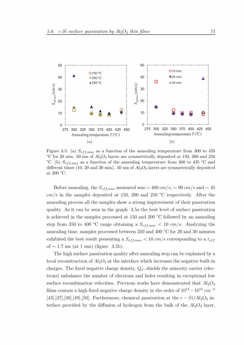
3.6. c-Si surface passivation by Al2O3 thin films 71
5050
150 ºC
40
150 ºC
40 200 ºC
) 250 ºC
/s) 50 C
30m/
(cm
ax
20eff,
m
20
Sef
1010
00
275 300 325 350 375 400 425 450
Annealing temperature T (ºC)Annealing temperature T ( C)
(a)
5050
10 min
40 20 min40 20 min
) 30 min
/s) 30 min
30
cm/
(cm
ax
20eff,
m
20
Sef
1010
00
275 300 325 350 375 400 425 450
Annealing temperature T (ºC)Annealing temperature T ( C)
(b)
Figure 3.5: (a) Seff,max as a function of the annealing temperature from 300 to 435°C for 20 min. 50 nm of Al2O3 layers are symmetrically deposited at 150, 200 and 250°C. (b) Seff,max as a function of the annealing temperature from 300 to 435 °C anddifferent times (10, 20 and 30 min). 50 nm of Al2O3 layers are symmetrically depositedat 200 °C.
Before annealing, the Seff,max measured was ∼ 480 cm/s, ∼ 90 cm/s and ∼ 45
cm/s in the samples deposited at 150, 200 and 250 °C respectively. After the
annealing process all the samples show a strong improvement of their passivation
quality. As it can be seen in the graph 3.5a the best level of surface passivation
is achieved in the samples processed at 150 and 200 °C followed by an annealing
step from 350 to 400 °C range obtaining a Seff,max < 10 cm/s. Analyzing the
annealing time, samples processed between 350 and 400 °C for 20 and 30 minutes
exhibited the best result presenting a Seff,max < 10 cm/s corresponding to a τeff
of ∼ 1.7 ms (at 1 sun) (figure 3.5b).
The high surface passivation quality after annealing step can be explained by a
local reconstruction of Al2O3 at the interface which increases the negative built-in
charges. The fixed negative charge density, Qf , shields the minority carrier (elec-
trons) unbalance the number of electrons and holes resulting in exceptional low
surface recombination velocities. Previous works have demonstrated that Al2O3
films contain a high fixed negative charge density in the order of 1012 −1013 cm−2
[43],[47],[48],[49],[50]. Furthermore, chemical passivation at the c − Si/Al2O3 in-
terface provided by the diffusion of hydrogen from the bulk of the Al2O3 layer,

72 Chapter 3. c-Si surface passivation by Al2O3 thin films
reduces defect related recombination [47],[48],[49],[50],[51] improving even more
the passivation.
Another important fact that should be mentioned is the blistering effect de-
tected at the samples processed at 150 °C followed by a post-annealing temper-
ature higher than 350 °C and at the remaining samples annealed above 435 °C
(Figure 3.6). This effect consists of the partial delamination of the Al2O3 film and
the corresponding bubble formation is attributed to the local accumulation and
release of gaseous hydrogen and/or H2O from the layer upon thermal treatments
above a critical temperature [52],[53],[54]. The higher the annealing temperature
is, the higher the bubble density and bubble radii are. Despite the blistering
phenomenon in some samples, effective lifetime measurements still evidenced a
good passivation quality after the annealing step.
Figure 3.6: Optical microscope images of the blistering effect. The sample with 50nmof Al2O3 was deposited at 150 oC. Image shows bubbles of 8 µm radius and 200bubbles/mm2 density
3.6.3 Influence of Al2O3 thickness on surface recombina-
tion velocity
Influence of Al2O3 thickness on the passivation quality is also studied. Samples
under test are ALD processed at 200 °C and 1.4, 6.5, 14, 25 and 50 nm (corres-
ponding to 13, 59, 127, 227 and 455 cycles) of Al2O3 are deposited after a RCA
cleaning. Then, the samples are annealed at different temperatures and time.
Seff,max results are displayed in Figure 3.7.
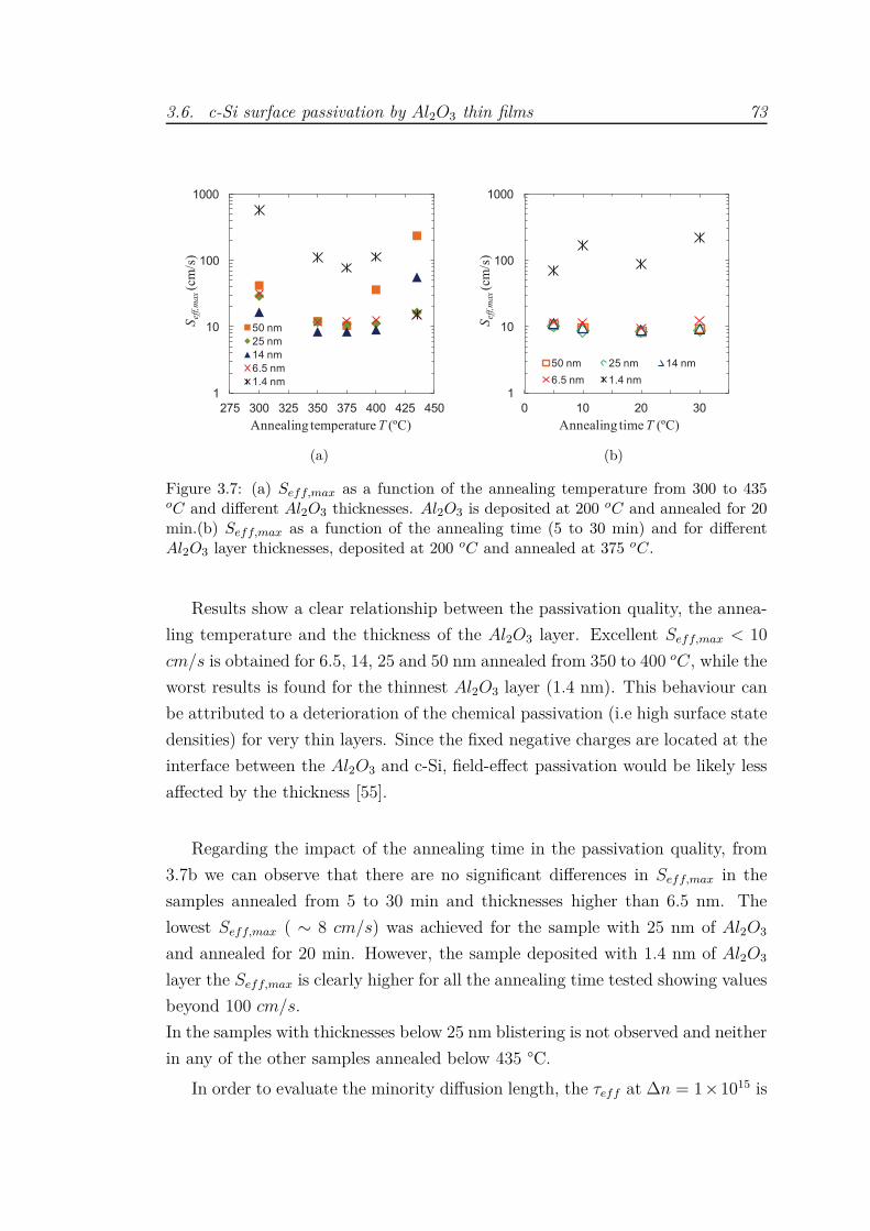
3.6. c-Si surface passivation by Al2O3 thin films 73
1
10
100
1000
275 300 325 350 375 400 425 450
Sef
f,m
ax(c
m/s
)
Annealing temperature T (ºC)
50 nm
25 nm
14 nm
6.5 nm
1.4 nm
(a)
1
10
100
1000
0 10 20 30
Sef
f,m
ax(c
m/s
)
Annealing time T (ºC)
50 nm 25 nm 14 nm
6.5 nm 1.4 nm
(b)
Figure 3.7: (a) Seff,max as a function of the annealing temperature from 300 to 435oC and different Al2O3 thicknesses. Al2O3 is deposited at 200 oC and annealed for 20min.(b) Seff,max as a function of the annealing time (5 to 30 min) and for differentAl2O3 layer thicknesses, deposited at 200 oC and annealed at 375 oC.
Results show a clear relationship between the passivation quality, the annea-
ling temperature and the thickness of the Al2O3 layer. Excellent Seff,max < 10
cm/s is obtained for 6.5, 14, 25 and 50 nm annealed from 350 to 400 oC, while the
worst results is found for the thinnest Al2O3 layer (1.4 nm). This behaviour can
be attributed to a deterioration of the chemical passivation (i.e high surface state
densities) for very thin layers. Since the fixed negative charges are located at the
interface between the Al2O3 and c-Si, field-effect passivation would be likely less
affected by the thickness [55].
Regarding the impact of the annealing time in the passivation quality, from
3.7b we can observe that there are no significant differences in Seff,max in the
samples annealed from 5 to 30 min and thicknesses higher than 6.5 nm. The
lowest Seff,max ( ∼ 8 cm/s) was achieved for the sample with 25 nm of Al2O3
and annealed for 20 min. However, the sample deposited with 1.4 nm of Al2O3
layer the Seff,max is clearly higher for all the annealing time tested showing values
beyond 100 cm/s.
In the samples with thicknesses below 25 nm blistering is not observed and neither
in any of the other samples annealed below 435 °C.
In order to evaluate the minority diffusion length, the τeff at ∆n = 1×10¹⁵ is
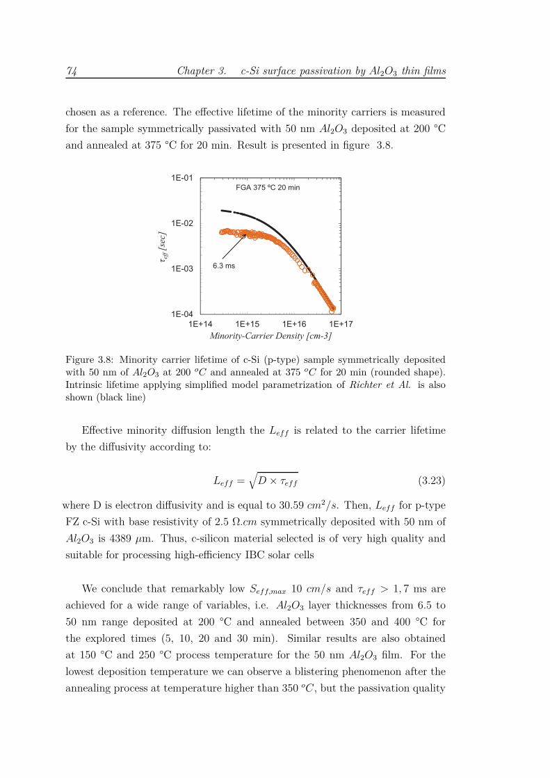
74 Chapter 3. c-Si surface passivation by Al2O3 thin films
chosen as a reference. The effective lifetime of the minority carriers is measured
for the sample symmetrically passivated with 50 nm Al2O3 deposited at 200 °C
and annealed at 375 °C for 20 min. Result is presented in figure 3.8.
eff[s
ec]
Minority-Carrier Density [cm-3]
Figure 3.8: Minority carrier lifetime of c-Si (p-type) sample symmetrically depositedwith 50 nm of Al2O3 at 200 oC and annealed at 375 oC for 20 min (rounded shape).Intrinsic lifetime applying simplified model parametrization of Richter et Al. is alsoshown (black line)
Effective minority diffusion length the Leff is related to the carrier lifetime
by the diffusivity according to:
Leff =√
D × τeff (3.23)
where D is electron diffusivity and is equal to 30.59 cm2/s. Then, Leff for p-type
FZ c-Si with base resistivity of 2.5 Ω.cm symmetrically deposited with 50 nm of
Al2O3 is 4389 µm. Thus, c-silicon material selected is of very high quality and
suitable for processing high-efficiency IBC solar cells
We conclude that remarkably low Seff,max 10 cm/s and τeff > 1, 7 ms are
achieved for a wide range of variables, i.e. Al2O3 layer thicknesses from 6.5 to
50 nm range deposited at 200 °C and annealed between 350 and 400 °C for
the explored times (5, 10, 20 and 30 min). Similar results are also obtained
at 150 °C and 250 °C process temperature for the 50 nm Al2O3 film. For the
lowest deposition temperature we can observe a blistering phenomenon after the
annealing process at temperature higher than 350 oC, but the passivation quality

3.6. c-Si surface passivation by Al2O3 thin films 75
is not apparently affected. It is also important to highlight that a good passivation
level is achieved (Seff,max < 100 cm/s ) for ultra-thin Al2O3 layers (∽ 1.4 nm).
3.6.4 Al2O3/a − SiCx surface passivating stacks.
Experimental
In the previous experiment, we showed that Al2O3 on p-type polished c-Si subs-
trates annealed between 350 and 400 °C (< 435 °C) from 10 to 20 min is enough
to obtain an excellent passivation . The aim of this experimental is to comple-
ment the preceding work studying the surface recombination velocity on both n-
and p-type polished and randomly textured wafers passivated with Al2O3/a-SiCx
stacks as well as their optical characterization. The reason to include the stoichio-
metric a-SiCx as capping layer on Al2O3 is because it has been demonstrated that
it improves the laser contact formation on p-type c-Si solar cells in comparison to
the typical Laser Fired Contact (LFC) process [56],[57]. Additionally, SiCx layer
is needed for chemical protection purposes of the Al2O3 films in cleaning/etching
steps during the IBC fabrication process.
Samples under test where symmetrically deposited with 25, 35, 50 and 90
nm of Al2O3 and complemented up to 75 nm total with stoichiometric a − SiCx
deposited by PECVD. As exception, the sample with 90 nm of Al2O3 will be
evaluated without the extra capping layer as a reference of antireflection without
SiCx. Test structures are shown in Figure 3.9.
c Si Al2O3a SiCx
(a) Planar text
c Sic Si
º
(b) Textured test
Figure 3.9: Symmetrical test structures for the measurements of τeff
The experimental starts with four FZ c-Si wafers (4 inches). Two are p-type
and two n-type. For both types the resistivity is about 2.5± 0.5 Ωcm and 280
µm thickness. One p-type and one n-type wafers are both side randomly textured
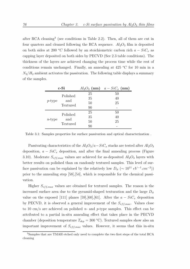
76 Chapter 3. c-Si surface passivation by Al2O3 thin films
after RCA cleaning3 (see conditions in Table 2.2). Then, all of them are cut in
four quarters and cleaned following the RCA sequence. Al2O3 film is deposited
on both sides at 200 oC followed by an stoichiometric carbon rich a − SiCx as
capping layer deposited on both sides by PECVD (See 2.3 table conditions). The
thickness of the layers are achieved changing the process time while the rest of
conditions remain unchanged. Finally, an annealing at 425 oC for 10 min in a
N2/H2 ambient activates the passivation. The following table displays a summary
of the samples.
c-Si Al2O3 (nm) a − SiCx (nm)
p-typePolished
andTextured
25 5035 4050 2590 -
n-typePolished
andTextured
25 5035 4050 2590 -
Table 3.1: Samples properties for surface passivation and optical characterization .
Passivating characteristics of the Al2O3/a−SiCx stacks are tested after Al2O3
deposition, a − SiCx deposition, and after the final annealing process (Figure
3.10). Moderate Seff,max values are achieved for as-deposited Al2O3 layers with
better results on polished than on randomly textured samples. This level of sur-
face passivation can be explained by the relatively low Dit (∼ 1011 eV −1.cm−2))
prior to the annealing step [58],[54], which is responsible for the chemical passi-
vation.
Higher Seff,max values are obtained for textured samples. The reason is the
increased surface area due to the pyramid-shaped texturation and the large Dit
value on the exposed [111] planes [59],[60],[61]. After the a − SiCx deposition
by PECVD, it is observed a general improvement of the Seff,max. Values close
to 10 cm/s are achieved on polished n- and p-type samples. This effect can be
attributed to a partial in-situ annealing effect that takes place in the PECVD
chamber (deposition temperature Tdep = 300 °C). Textured samples show also an
important improvement of Seff,max values. However, it seems that this in-situ
3Samples that are TMAH etched only need to complete the two first steps of the total RCAcleaning
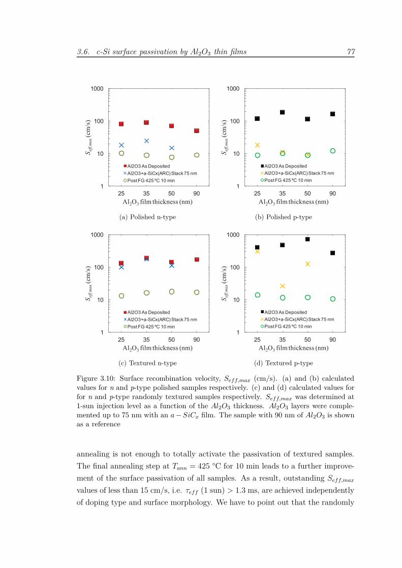
3.6. c-Si surface passivation by Al2O3 thin films 77
1
10
100
1000
25 35 50 90
Seff,max(c
m/s
)
Al2O3 film thickness (nm)
Al2O3 As Deposited
Al2O3+a-SiCx(ARC) Stack 75 nm
Post FG 425 ºC 10 min
(a) Polished n-type
1
10
100
1000
25 35 50 90
Seff,max(c
m/s
)
Al2O3 film thickness (nm)
Al2O3 As Deposited
Al2O3+a-SiCx(ARC) Stack 75 nm
Post FG 425 ºC 10 min
(b) Polished p-type
1
10
100
1000
25 35 50 90
Seff,max(c
m/s
)
Al2O3 film thickness (nm)
Al2O3 As Deposited
Al2O3+a-SiCx(ARC) Stack 75 nm
Post FG 425 ºC 10 min
(c) Textured n-type
1
10
100
1000
25 35 50 90
Seff,max(c
m/s
)
Al2O3 film thickness (nm)
Al2O3 As Deposited
Al2O3+a-SiCx(ARC) Stack 75 nm
Post FG 425 ºC 10 min
(d) Textured p-type
Figure 3.10: Surface recombination velocity, Seff,max (cm/s). (a) and (b) calculatedvalues for n and p-type polished samples respectively. (c) and (d) calculated values forfor n and p-type randomly textured samples respectively. Seff,max was determined at1-sun injection level as a function of the Al2O3 thickness. Al2O3 layers were comple-mented up to 75 nm with an a − SiCx film. The sample with 90 nm of Al2O3 is shownas a reference
annealing is not enough to totally activate the passivation of textured samples.
The final annealing step at Tann = 425 °C for 10 min leads to a further improve-
ment of the surface passivation of all samples. As a result, outstanding Seff,max
values of less than 15 cm/s, i.e. τeff (1 sun) > 1.3 ms, are achieved independently
of doping type and surface morphology. We have to point out that the randomly

78 Chapter 3. c-Si surface passivation by Al2O3 thin films
textured sample require higher annealing temperatures (425 °C) than polished
ones to achieve similar Seff,max.
The previous experimental demonstrates that Tann = 375 °C is enough to
activate the surface passivation on polished substrates. In fact, some polished
samples already showed an optimum passivation quality just after the PECVD
process due to the in-situ annealing. On the other hand, an annealing of 425 °C
is the critical limit to avoid a blistering effect, which we have previously observed
on polished samples with Al2O3 films.
Regarding the effect of the film thickness, it is interesting to note that a rather
constant high level of surface passivation is obtained after the annealing of the
whole range of Al2O3 thicknesses with a − SiCx capping layer agreeing with the
study realized in previous section with only Al2O3 . It can be deduced that fixed
negative charges located at the interface between Al2O3 are not affected by the
introduction of the additional layer.
3.6.5 Al2O3/a − SiCx stacks. Optical characterization.
Optical losses in IBC solar cells are heavily reduced due to the absence of the
metal finger grid on the front side. However, there are still other remaining optical
losses that include surface reflectance and film parasitic absorption.
In order to achieve an optimal conversion efficiency of IBC solar cells the
application of a so-called antireflection coating (ARC) in combination with surface
texturing techniques plays an important role in reducing reflection losses [62]. The
minimum reflectance should be located at about λ = 600 nm where the maximum
photon flow for spectrum AM 1.5g occurs.
In this study, the antireflection behaviour of the different combinations of
Al2O3 and Al2O3/ stoichiometric a-SiCx stack deposited on c-Si substrates pro-
posed in the previous section is evaluated.
Refractive index is measured by ellipsometry resulting in
nAl2O3= 1.6 and na−SiCx
= 2.0. Simple simulations demonstrate that the opti-
mum thickness for the total stack is 75 nm. Figure 3.11 shows the simulated
reflectance for three thickness combinations on polished c-Si surface.
Reflectance measurements corresponding to samples described in Table 3.1 are
measured with UV-VIS-NIR spectrometer equipped with an integrating sphere
over the wavelength range from 300 to 1200 nm. These measurements are taken
after the Al2O3 deposition and after a − SiCx deposition. Both results are pre-

3.6. c-Si surface passivation by Al2O3 thin films 79
Ref
lect
ance
(%
)
Figure 3.11: The graph shows the simulated reflectance of double layer antireflectioncoating. Different thickness of Al2O3 and a-SiCx are displayed resulting in a total stackthickness of 75 nm. Source www.pveducation.org/pvcdrom/design/dlarc
sented in Figure 3.12. It must be mentioned that no significant differences were
found between n- and p-type c-Si substrates.
As it can be observed the textured sample without ARC exhibits an integrated
reflectance average of 13.3%, much lower than that of polished c-Si substrates.
For a randomly textured surface, the reduced reflection is explained by a second
reflection of the incident light at the side walls of an opposite pyramid [63]. After
coating the silicon substrates, optical reflectance was further reduced in all cases.
When a single layer antireflection coating covers the polished c-Si samples (Graph
3.12a) the reflectance yields to a minimum of 3.2% at 600 nm wavelength in case
of 90 nm thick quickly increasing for wavelengths shorter and longer. Further-
more, reflectance properties are worse as the film thickness decreases. However,
when the single layer ARC is deposited on textured c-Si samples reflectance is
strongly reduced (Graph 3.12b). We can observe a flattering response of the
reflectance curves on the whole studied range. The values measured are < 2%
from 460 nm to 1000 nm when a textured c-Si sample is coated by 90 nm of
Al2O3. Reflectance slightly increases when ARC thickness decreases.
When 75 nm of double-layer antireflection coatings are deposited on c-Si sam-
ples (polished (Graph 3.12c) and textured (Graph 3.12d), the whole range of
reflection measurements are clearly lower (the total stack have the optimum thick-
ness). In the case of textured samples, reflectance is lower than 2% from 460 nm
to 1050 nm for all the stack configurations.
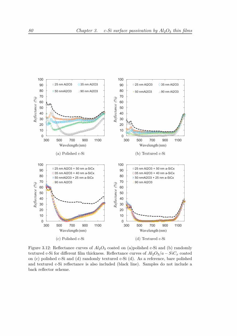
80 Chapter 3. c-Si surface passivation by Al2O3 thin films
0
10
20
30
40
50
60
70
80
90
100
300 500 700 900 1100
Ref
lect
an
ce (
%)
Wavelength (nm)
25 nm Al2O3 35 nm Al2O3
50 nmAl2O3 90 nm Al2O3
(a) Polished c-Si
0
10
20
30
40
50
60
70
80
90
100
300 500 700 900 1100
Ref
lect
an
ce (
%)
Wavelength (nm)
25 nm Al2O3 35 nm Al2O3
50 nmAl2O3 90 nm Al2O3
(b) Textured c-Si
0
10
20
30
40
50
60
70
80
90
100
300 500 700 900 1100
Ref
lect
an
ce (
%)
Wavelength (nm)
25 nm Al2O3 + 50 nm a-SiCx
35 nm Al2O3 + 40 nm a-SiCx
50 nmAl2O3 + 25 nm a-SiCx
90 nm Al2O3
(c) Polished c-Si
0
10
20
30
40
50
60
70
80
90
100
300 500 700 900 1100
Ref
lect
an
ce (
%)
Wavelength (nm)
25 nm Al2O3 + 50 nm a-SiCx
35 nm Al2O3 + 40 nm a-SiCx
50 nmAl2O3 + 25 nm a-SiCx
90 nm Al2O3
(d) Textured c-Si
Figure 3.12: Reflectance curves of Al2O3 coated on (a)polished c-Si and (b) randomlytextured c-Si for different film thickness. Reflectance curves of Al2O3/a − SiCx coatedon (c) polished c-Si and (d) randomly textured c-Si (d). As a reference, bare polishedand textured c-Si reflectance is also included (black line). Samples do not include aback reflector scheme.

3.6. c-Si surface passivation by Al2O3 thin films 81
R
A
Borofloat
Al2O3
a SiCx
T
Figure 3.13: Borofloat test structure for absorbance measurements
0
5
10
15
20
25
300 400 500 600
Ab
sorb
an
ce (
%)
Wavelength (nm)
25 nm Al2O3 + 50 nm a-SiCx(ARC)
35 nm Al2O3 + 40 nm a-SiCx(ARC)
50 nm Al2O3 + 25 nm a-SiCx (ARC)
90 nm Al2O3
Figure 3.14: Absorbance as a function of the wavelength in the range of 300 to 600 nmof different stacks configurations and 90 nm Al2O3.
Absorbance is another optical parameters studied in order to know the quan-
tity of light absorbed by the Al2O3/a−SiCx stacks. To do so, borofloat substrates
are one side deposited with the different stacks configurations and analysed be-
tween 300 to 600 nm range (Figure 3.13). The absorbance stack is calculated
from the reflectance and transmittance measurements and the results are shown
in figure 3.14.
Other works have previously reported an optical bandgap of Eopt = 6.4 ± 0.1
eV for as-deposited and annealed ALD Al2O3 films [54], which means that this
material is transparent for wavelengths above 200 nm. Therefore, absorption
of light by the Al2O3 layer does not occur in the wavelength range relevant for
82 Chapter 3. c-Si surface passivation by Al2O3 thin films
photovoltaic applications. This property is experimentally confirmed by the 90
nm Al2O3 sample results (see figure 3.14). For the sake of clarity, only the 300
to 600 nm wavelength range is depicted, i.e. where a relevant absorbance can
exist. However, it can be seen that as the a − SiCx layer thickness increases, the
optical absorbance also increases up to a value of 21.1% at 300 nm. Then, the
SiCx capping layer is less attractive to be used as an antireflection layer on the
illuminated side of the solar cell compared to a single 90 nm Al2O3 film.
3.7 CONCLUSION
Al2O3 layers and Al2O3/a − SiCx stacks with different thickness were deposited
on polished and randomly textured p- and n-type c-Si substrates by combining
thermal ALD and PECVD technique. Outstanding Seff,max values below 15 cm/s
were achieved independently of the surface morphology and doping type of the
samples. This value is low enough to obtain highly efficient c-Si IBC solar cells.
Concerning the optical properties, the absorbance of Al2O3 layers with differ-
ent thickness and also of different Al2O3/a−SiCx stacks was calculated by evalu-
ating reflectance and transmittance measurements. We found that optical losses
due to the absorption of a − SiCx layers in the range of short wavelengths is the
reason for the superior overall optical performance of a single 90 nm thick Al2O3
film. Therefore, the latter represents the better option as an antireflection coating
compared to Al2O3/a − SiCx stacks. This result is supported by the reflectance
measurements of Al2O3 films with different thickness and Al2O3/a − SiCx stacks
on polished and textured c-Si substrates in the wavelength range from 300 to
1200 nm. In any case, the measured reflectance was less than 2% for all the
Al2O3/a − SiCx stacks and also for the single 90 nm layer of Al2O3. Neverthe-
less, an a − SiCx capping layer could be useful if the Al2O3 layer needs to be
protected from some chemical treatment during the solar cell fabrication. More-
over, on the rear side of a c-Si solar cell, where the optical absorbance is not
critical, an a − SiCx layer on top of the passivated Al2O3 film acts as a back
reflector that reflects photons towards the c-Si bulk. This a − SiCx capping layer
on the Al2O3 also improves the laser contact formation on c-Si solar cells.
Bibliography 83
Bibliography
[1] W. Shockley and W. Read. Statistics of the recombinations of holes and
electrons. Physical Review, 87:835–842, 1952.
[2] Armin G. Aberle. Crystalline Silicon Solar Cells: Advanced Surface Passi-
vation and Analysis. 1999.
[3] W. Michaelis and M. H. Pilkuhn. Radiative recombination in silicon p-n
junctions. physica status solidi (b), 36:311–319, 1969.
[4] M. Ruff, M. Fick, R. Lindner, U. Rössler, and R. Helbig. The spectral
distribution of the intrinsic radiative recombination in silicon. Journal of
Applied Physics, 74:267–274, 1993.
[5] H. Schlangenotto, H. Maeder, and W. Gerlach. Temperature dependence of
the radiative recombination coefficient in silicon. Physica Status Solidi (a),
357(21):357–367, 1974.
[6] T. Trupke, M. A. Green, P. Wurfel, P.P. Altermatt, A. Wang, J. Zhao,
and R. Corkish. Temperature dependence of the radiative recombination
coefficient of intrinsic crystalline silicon. Journal of Applied Physics, 94:
4930–4937, 2003.
[7] A. Hangleiter and R. Häcker. Enhancement of band-to-band auger recom-
bination by electron-hole correlations. Physical Review Letters, 65:215–218,
1990.
[8] J. Dziewior and W. Schmid. Auger coefficients for highly doped and highly
excited silicon. Applied Physics Letters, 31:346, 1977.
[9] M. Kerr and A. Cuevas. General parameterization of auger recombination
in crystalline silicon. Journal of Applied Physics, 91:2473, 2002.
[10] A. Richter, S.W. Glunz, F. Werner, J. Schmidt, and A. Cuevas. Physical
Review B.
[11] R. Hall. Electron-hole recombination in germanium. Physical Review, 87:
387–387, 1952.

84 Bibliography
[12] J. Schmidt and A.G. Aberle. Accurate method for the determination of
bulk minority-carrier lifetimes of mono- and multicrystalline silicon wafers.
Journal of Applied Physics, 81:6186, 1997.
[13] M.A. Green. Advanced Principles and Practice. Sydney:UNSW, 1995.
[14] Armin G Aberle. Surface passivation of crystalline silicon solar cells: a
review. Progress in Photovoltaics: Research and Applications, 8:473–487,
2000.
[15] Pietro P. Altermatt, Jürgen O. Schumacher, A. Cuevas, M.J Kerr, S. W
Glunz, Richard R. King, G. Heiser, and A. Schenk. Numerical modeling of
highly doped si:p emitters based on fermi- dirac statistics and self-consistent
material parameters. Journal of Applied Physics, 92(6):3187, 2002.
[16] Armin G. Aberle, S. Glunz, and W. Warta. Impact of illumination level and
oxide parameters on shockley-read-hall recombination at the si-sio2 interface.
Journal of Applied Physics, 71:4422, 1992.
[17] S. W Glunz, D. Biro, S. Rein, and W. Warta. Field-effect passivation of the
sio2-si interface. Journal of applied Physics, 86:683, 1999.
[18] M. Kerr and A. Cuevas. Very low bulk and surface recombination in oxidized
silicon wafers. Semiconductor Science and Technology, 17:35–38, 2002.
[19] J Zhao, A Wang, and M.A Green. 24.5% efficiency pert silicon solar cells on
seh mcz substrates and cell performance on other seh cz and fz substrates.
Solar Energy Materials and Solar Cells, 2001.
[20] R. Hezel and K. Jaeger. Low-temperature surface passivation of silicon for
solar cells. Journal of the Electrochemical Society, 136:518–523, 1989.
[21] M. Kerr and A. Cuevas. Recombination at the interface between silicon and
stoichiometric plasma silicon nitride. Semiconductor Science and Technology,
17:166–172, 2002.
[22] M. Hofmann, S. Janz, C. Schmidt, S. Kambor, D. Suwito, N. Kohn,
J. Rentsch, R. Preu, and S.W Glunz. Recent developments in rear-surface
passivation at fraunhofer ise. Solar Energy Materials and Solar Cells, 93:
1074–1078, 2009.
Bibliography 85
[23] M. Schmidt, J.and Kerr and A. Cuevas. Surface passivation of silicon solar
cells using plasma-enhanced chemical-vapour-deposited sin films and thin
thermal sio2 /plasma sin stacks. Semiconductor Science and Technology, 16:
164–170, 2001.
[24] Y. Larionova, V. Mertens, N.P Harder, and R. Brendel. Surface passivation
of n-type Czochralski silicon substrates by thermal-SiO2/plasma-enhanced
chemical vapor deposition SiN stacks. Applied Physics Letters, 96:1–3, 2010.
[25] G Dingemans and M.M Mandoc. Effective passivation of Si surfaces by
plasma deposited SiOx/a-SiNx: H stacks. Applied Physics Letters, 98:
222102, 2011.
[26] P. Doshi, Gerald E. Jellison, and A. Rohatgi. Characterization and optimiza-
tion of absorbing plasma-enhanced chemical vapor deposited antireflection
coatings for silicon photovoltaics. Applied Optics, 36:7826, 1997.
[27] J. Schmidt, J.D. Moschner, J. Henze, S. Dauwe, and R. Hezel. Recent
progress in the surface passivation of silicon solar cells using silicon nitride.
In 19th European Photovoltaic Solar Energy Conference, Paris, France, 7-11
June 2004.
[28] Mark John Kerr. Surface, Emitter and Bulk Recombination in Silicon and
Development of Silicon Nitride Passivated Solar Cells. PhD thesis, 2002.
[29] S. Kerdiles, R. Madelon, and R. Rizk. Spectroscopic ellipsometry analysis of
nanocrystalline silicon carbide obtained at low temperature. Applied surface
Science, 184:150–155, 2001.
[30] I. Martin, M. Vetter, A. Orpella, C. Voz, J. Puigdollers, and R. Alcubilla.
Characterization of p-type c-si surface passivation by n-doped a-sicx:h films.
In Proceedings of the 17th European Photovoltaic Solar Energy Conference,
Munich, pages 2954–2957, 2001.
[31] R. Ferre, A. Orpella, D. Munoz, I. Martin, F. Recart, C. Voz, J. Puigdollers,
P. Cabarrocas, and R Alcubilla. Very low surface recombination velocity
of crystalline silicon passivated by phosphorus-doped a-sicxny:h(n) alloys.
Progress in Photovoltaics: Research Appl., 16:123–127, 2008.
86 Bibliography
[32] R. Ferre, I. Martin, P. Ortega, M. Vetter, I. Torres, and R. Alcubilla. n-
type emitter surface passivation in c-si solar cells by means of antireflective
amorphous silicon carbide layers. Journal of Applied Physics, 100:073703–
073710, 2006.
[33] R. Ferre, I. Martín, P. Ortega, and M. Vetter. n-type emitter surface passi-
vation in c-si solar cells by means of antireflective amorphous silicon carbide
layers. Journal of Applied Physics, 100:073703, 2006.
[34] A. Morales-Vilches, C. Voz, M. Colina, G. Lopez, I. Martin, A. Orpella,
J. Puigdollers, M. Garcia, and R. Alcubilla. Progress in silicon heterojunction
solar cell fabrication with rear laser-fired contacts. In Proceedings of the 2013
Spanish Conference on Electron Devices, CDE 2013, pages 345–348, 2013.
[35] I. Martín, M. Colina, A. Orpella, C. Voz, S. De Vecchi, T. Desrues, S. Abol-
masov, P. Roca i Cabarrocas, and R. Alcubilla. Low recombination n+ re-
gions created by n+ c-si epitaxial layers and laser processing of phosphorus-
doped sicx films. In 27th European Photovoltaic Solar Energy Conference
and Exhibition, pages 1519–1523, 2012.
[36] I. Martín, M. Colina, A. Coll, G. López, P. Ortega, A. Orpella, and R. Al-
cubilla. c-si solar cells based on laser-processed dielectric films. Energy
Procedia, 55:255–264, 2014.
[37] S. Dauwe, J. Schmidt, and R. Hezel. Very low surface recombination veloci-
ties on p- and n-type silicon wafers passivated with hydrogenated amorphous
silicon films. In Conference Record of the Twenty-Ninth IEEE Photovoltaic
Specialists Conference, 2002, pages 1246–1249. IEEE, 2002.
[38] S.W. Glunz, A. Grohe, M. Hermle, and et Al. Comparison of different dielec-
tric passivation layers for application in industrially feasible high-efficiency
crystalline silicon solar cells. In 20th European Photovoltaic Solar Energy
Conference 2005. Proceedings, pages 572–577, 2005.
[39] A. Bentzen, A. Ulyashin, A. Suphellen, E. Sauar, D. Grambole, D.N. Wright,
E.S. Marstein, B.G. Svensson, and A. Holt. Surface passivation of silicon
solar cells by amorphous silicon/silicon nitride dual layers. In 15th Interna-
tional Photovoltaic Science & Engineering Conference (PVSEC-15), pages
316–317, 2005.
Bibliography 87
[40] H. Plagwitz, Y. Takahashi, B. Terheiden, and R. Brendel. Amorphous si/sin
double layers: A low temperature passivation method for diffused phospho-
rus as well as boron emitters. In 21st European Photovoltaic Solar Energy
Conference, page 688, 2006.
[41] F. Werner, B. Veith, V. Tiba, P. Poodt, F. Roozeboom, R. Brendel, and
J. Schmidt. Very low surface recombination velocities on p- and n-type c-
si by ultrafast spatial atomic layer deposition of aluminum oxide. Applied
Physics Letters, 97:162103, 2010.
[42] B. Hoex, M. C. M. Van de Sanden, J. Schmidt, R. Brendel, and W. M. M.
Kessels. Surface passivation of phosphorus-diffused n+-type emitters by
plasma-assisted atomic-layer deposited al2o3. physica status solidi (RRL)
- Rapid Research Letters, 6:4–6, 2012.
[43] G. Agostinelli, A. Delabie, P. Vitanov, Z. Alexieva, H.F.W. Dekkers,
S. De Wolf, and G. Beaucarne. Very low surface recombination velocities on
p-type silicon wafers passivated with a dielectric with fixed negative charge.
Solar Energy Materials and Solar Cells, 90:3438–3443, 2006.
[44] B. Hoex, J. Schmidt, R. Bock, Pietro P. Altermatt, MCM Van de Sanden,
and WMM Kessels. Excellent passivation of highly doped p-type Si surfaces
by the negative-charge-dielectric Al2O3. Applied Physics Letters, 91(11):
112107, 2007.
[45] F. Granek. High-Efficiency Back-Contact Back-Junction Silicon Solar Cells.
PhD thesis, Fraunhofer Institut fur Solare Energiesysteme (ISE), July 2009.
[46] M.A. Green, A.W. Blakers, J. Shi, E.M. Keller, and S.R. Wenham. High-
efficiency silicon solar cells. IEEE Transactions on electron devices, 5:679–
683, 1984.
[47] B. Hoex, J. Schmidt, P. Pohl, M. C. M. van de Sanden, and W. M. M.
Kessels. Silicon surface passivation by atomic layer deposited al2o3. Journal
of Applied Physics, 104:044903, 2008.
[48] G. Dingemans, M. C. M. van de Sanden, and W. M. M. Kessels. Influence of
the Deposition Temperature on the c-Si Surface Passivation by Al2O3 Films
Synthesized by ALD and PECVD. Electrochemical and Solid-State Letters,
13:H76, 2010.
88 Bibliography
[49] J. Schmidt, F. Werner, B. Veith, D. Zielke, S. Steingrube, P.P. Altermatt,
S. Gatz, T. Dullweber, and R. Brendel. Advances in the surface passivation
of silicon solar cells. Energy Procedia, 15:30–39, 2012.
[50] B. Hoex, S. B. S. Heil, E. Langereis, M. C. M. van de Sanden, and W. M. M.
Kessels. Ultralow surface recombination of c-Si substrates passivated by
plasma-assisted atomic layer deposited Al2O3. Applied Physics Letters, 89:
042112, 2006.
[51] M. Cho, HB. Park, J. Park, C.S. Hwang, JC. Lee, SJ. Oh, J. Jeong, K.S.
Hyun, HS. Kang, YW. Kim, and JH. Lee. Thermal annealing effects on
the structural and electrical properties of HfO2/Al2O3 gate dielectric stacks
grown by atomic layer deposition on Si substrates. Journal of applied physics,
94:2563–257, 2003.
[52] B. Vermang, H. Goverde, A. Lorenz, A. Uruena, G. Vereecke, J. Meersschaut,
E. Cornagliotti, A. Rothschild, J. John, J. Poortmans, and R. Mertens. On
the blistering of atomic layer deposited Al2O3 as Si surface passivation. In
2011 37th IEEE Photovoltaic Specialists Conference, pages 003562–003567,
jun 2011.
[53] B. Vermang, H. Goverde, A. Uruena, A. Lorens, E. Cornagliotti, Rothschild
A., J. John, J. Poortmans, and R. Mertens. Blistering in ALD Al2O3 passi-
vation layers as rear contacting for local Al BSF Si solar cells. Solar Energy
Materials and Solar Cells, pages 204–209, 2012.
[54] G. Dingemans and W. M. M. Kessels. Status and prospects of Al2O3 based
surface passivation schemes for silicon solar cells. Journal of Vacuum Science
& Technology A: Vacuum, Surfaces, and Films, 30:040802, 2012.
[55] G. Dingemans, R. Seguin, P. Engelhart, M. C. M. van de Sanden, and
W. M. M. Kessels. Silicon surface passivation by ultrathin Al2O3 films syn-
thesized by thermal and plasma atomic layer deposition. physica status solidi
(RRL) - Rapid Research Letters, 4:10–12, 2010.
[56] P. Ortega, I. Martín, G. Lopez, M. Colina, A. Orpella, C. Voz, and R. Alcu-
billa. p-type c-Si solar cells based on rear side laser processing of Al2O3/SiCx
stacks. Solar Energy Materials and Solar Cells, 106:80–83, 2012.
Bibliography 89
[57] I. Martín, P. Ortega, M. Colina, A. Orpella, G. López, and R. Alcubilla.
Laser processing of Al2O3/a−SiCx : H stacks: a feasible solution for the rear
surface of high-efficiency p-type c-Si solar cells. Progress in Photovoltaics:
Research and Applications, 21:1171–1175, 2012.
[58] G. Dingemans, N.M. Terlinden, D. Pierreux, H.B. Profijt, M.C.M. van de
Sanden, and W. M. M. Kessels. Influence of the Oxidant on the Chemical
and Field-Effect Passivation of Si by ALD Al2O3. Electrochemical and Solid-
State Letters, 14:H1–H4, 2011.
[59] Keith R. McIntosh and Luke P. Johnson. Recombination at textured silicon
surfaces passivated with silicon dioxide. Journal of Applied Physics, 105:
124520, 2009.
[60] H. Angermann. Passivation of structured p-type silicon interfaces: Effect of
surface morphology and wet-chemical pre-treatment. Applied Surface Sci-
ence, 254:8067–8074, 2008.
[61] P.A. Basore. Numerical modeling of textured silicon solar cells using PC-1D.
IEEE Transactions on Electron Devices, 37:337–343, 1990.
[62] Martin Green. High efficiency silicon solar cells. Trans Tech, 1987.
[63] J. Zhao and M.A. Green. Optimized antireflection coatings for high-efficiency
silicon solar cells. IEEE Transactions on Electron Devices, 38:1925–1934,
1991.

Chapter 4
Emitter formation using laser
doping technique on n- and
p-type c-Si substrates
In this chapter laser doping technique is used to create highly-doped
regions defined in a point-like structure to form n+/p and p+/n junc-
tions. In particular, phosphorous-doped amorphous silicon (a-Si (n-
type)) and aluminum oxide (Al2O3) layers are used as dopant sources.
Laser power and number of pulses per spot are explored to obtain the
optimum electrical behaviour of the junctions. The junctions are elec-
trically contacted and characterized by means of dark J-V measure-
ments. Additionally, a diluted HF treatment previous to front metalli-
zation has been explored in order to know its impact on the junction
quality. The objective of this study is to apply the best laser condition
on the rear side of the IBC solar cell to form the BSF and emitter in
a point-like structure.
4.1 Introduction
Lasers are widely used for different applications in the industry of solar cells
such as scribing grooves in buried contact solar cells [1], firing contacts in the
laser fired contact (LFC) structure [2],[3],[4], texturing surfaces [5],[6], ablating
dielectrics layers [7], among others. The introduction of laser processes to create
doped regions into crystalline silicon (c-Si) can avoid the use of dopant diffusion
91

92Chapter 4. Emitter formation using laser doping technique on n- and p-type
c-Si substrates
in conventional high temperature furnaces that represents one of the most expen-
sive and time-consuming processes in the fabrication line. Laser doping diffusion
(LD) relies upon laser ability to heat locally the semiconductor surface. Doping
happens during the melting phase of the silicon in which dopant is incorporated
(diffused) into the silicon structure [6],[8]. Several methods applying laser doping
technique (LD) to junction formation have been presented to date and a wide
variety of dopant source can be used in gas, liquid or solid form [9],[10],[11],[12].
In this experimental we apply the LD technique to create highly-doped regions
defined in a point-like structure to form n+/p and p+/n junctions applying a
pulsed Nd-YAG 1064 nm laser in the nanosecond regime. Dielectric layers de-
posited at low temperature have been used as dopant sources, particularly a
phosphorous-doped silicon carbide stack (a − SiCx(i)/a − Si : H (n-type)) de-
posited by PECVD and Al2O3 layer deposited by ALD. These layers have the
advantage that, if correctly tuned, they can also work as c-Si passivating layers
and reduce optical reflectance as it has been demonstrated in previous chapter
[13],[14]. Parameters such as pulse power and number of pulses are varied in order
to find the conditions leading to the optimal electrical behaviour of the formed
junction. The fabricated n+/p and p+/n junctions are electrically characterized
by means of dark J-V measurements. We analyze how the laser parameters and
the HF treatment previous metallization step impact on the J-V curves.
4.2 Experimental
4.2.1 Laser system
Laser doping is carried out using a pulsed Nd:YAG laser (Star-Mark SMP100
II Rofin-Baasel) working at 1064 nm wavelength in TEM00 mode, with a fixed
frequency of 4 kHz and a pulse duration fixed at 100 ns. The power of the
laser beam can be adjusted by varying the intensity of the continuous lamp that
pumps the Nd:YAG crystal. In this study, we explore the quality of the laser
doped regions varying the laser power from 0.8 W to 1.4 W and the number of
pulses per spot: 3, 6 and 9 pulses.
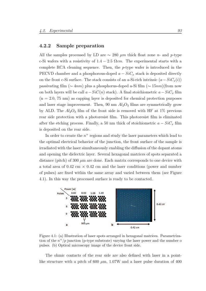
4.2. Experimental 93
4.2.2 Sample preparation
All the samples processed by LD are ∼ 280 µm thick float zone n- and p-type
c-Si wafers with a resistivity of 1.4 − 2.5 Ωcm. The experimental starts with a
complete RCA cleaning sequence. Then, the p-type wafer is introduced in the
PECVD chamber and a phosphorous-doped a − SiCx stack is deposited directly
on the front c-Si surface. The stack consists of an a-Si-rich intrinsic (a−SiCx(i))
passivating film (∼ 4nm) plus a phosphorus-doped a-Si film (∼ 15nm)(from now
on both layers will be call a−SiC(n) stack). A final stoichiometric a−SiCx film
(n = 2.0, 75 nm) as capping layer is deposited for chemical protection purposes
and laser stage improvement. Then, 90 nm Al2O3 films are symmetrically grow
by ALD. The Al2O3 film of the front side is removed with HF at 1% previous
rear side protection with a photoresist film. This photoresist film is eliminated
after the etching process. Finally, a 50 nm thick of stoichiometric a − SiCx film
is deposited on the rear side.
In order to create the n+ regions and study the laser parameters which lead to
the optimal electrical behavior of the junction, the front surface of the sample is
irradiated with the laser simultaneously enabling the diffusion of the dopant atoms
and opening the dielectric layer. Several hexagonal matrices of spots separated a
distance (pitch) of 300 µm are done. Each matrix corresponds to one device with
a total area of 0.42 cm × 0.42 cm and the laser conditions (power and number
of pulses) are fixed within the same array and varied between them (see Figure
4.1). In this way the processed surface is ready to be contacted.
Figure 4.1: (a) Illustration of laser spots arranged in hexagonal matrices. Parametriza-tion of the n+/p junction (p-type substrate) varying the laser power and the number opulses. (b) Optical microscopy image of the device front side.
The ohmic contacts of the rear side are also defined with laser in a point-
like structure with a pitch of 600 µm, 1.07W and a laser pulse duration of 400
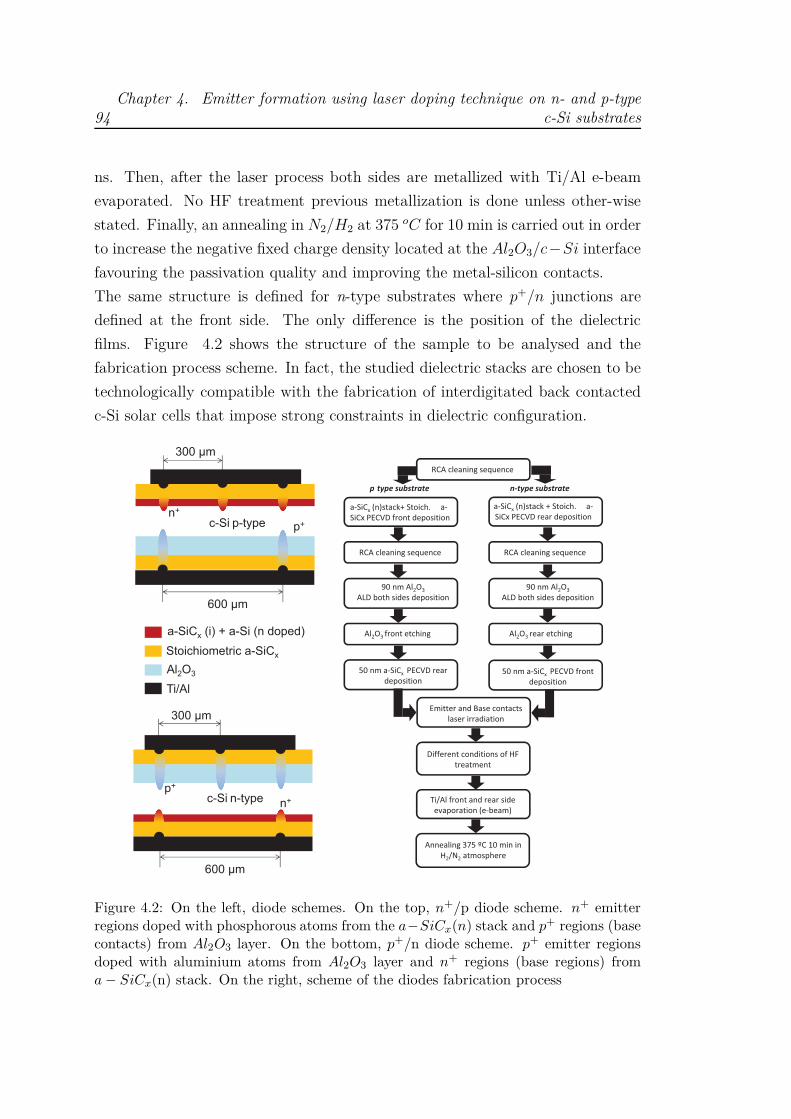
94Chapter 4. Emitter formation using laser doping technique on n- and p-type
c-Si substrates
ns. Then, after the laser process both sides are metallized with Ti/Al e-beam
evaporated. No HF treatment previous metallization is done unless other-wise
stated. Finally, an annealing in N2/H2 at 375 oC for 10 min is carried out in order
to increase the negative fixed charge density located at the Al2O3/c−Si interface
favouring the passivation quality and improving the metal-silicon contacts.
The same structure is defined for n-type substrates where p+/n junctions are
defined at the front side. The only difference is the position of the dielectric
films. Figure 4.2 shows the structure of the sample to be analysed and the
fabrication process scheme. In fact, the studied dielectric stacks are chosen to be
technologically compatible with the fabrication of interdigitated back contacted
c-Si solar cells that impose strong constraints in dielectric configuration.
5_3
Annealing 375 ºC 10 min in
H2/N2 atmosphere
RCA cleaning sequence
p type substrate n type substrate
a SiCx (n)stack+ Stoich. a
SiCx PECVD front deposition
90 nm Al2O3
ALD both sides deposition
Al2O3 front etching
Emitter and Base contacts
laser irradiation
Different conditions of HF
treatment
Ti/Al front and rear side
evaporation (e beam)
50 nm a SiCx PECVD rear
deposition
a SiCx (n)stack + Stoich. a
SiCx PECVD rear deposition
RCA cleaning sequence RCA cleaning sequence
90 nm Al2O3
ALD both sides deposition
Al2O3 rear etching
50 nm a SiCx PECVD front
deposition
Figure 4.2: On the left, diode schemes. On the top, n+/p diode scheme. n+ emitterregions doped with phosphorous atoms from the a−SiCx(n) stack and p+ regions (basecontacts) from Al2O3 layer. On the bottom, p+/n diode scheme. p+ emitter regionsdoped with aluminium atoms from Al2O3 layer and n+ regions (base regions) froma − SiCx(n) stack. On the right, scheme of the diodes fabrication process
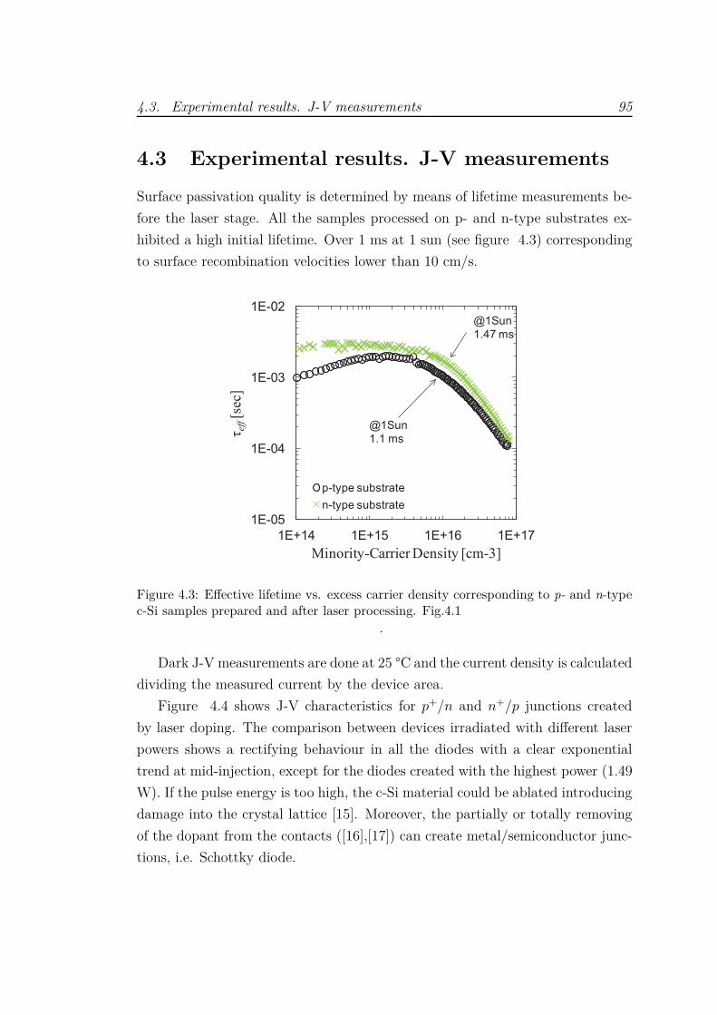
4.3. Experimental results. J-V measurements 95
4.3 Experimental results. J-V measurements
Surface passivation quality is determined by means of lifetime measurements be-
fore the laser stage. All the samples processed on p- and n-type substrates ex-
hibited a high initial lifetime. Over 1 ms at 1 sun (see figure 4.3) corresponding
to surface recombination velocities lower than 10 cm/s.
1E-05
1E-04
1E-03
1E-02
1E+14 1E+15 1E+16 1E+17
ef
f[s
ec]
Minority-Carrier Density [cm-3]
p-type substrate
n-type substrate
@1Sun
1.47 ms
@1Sun
1.1 ms
Figure 4.3: Effective lifetime vs. excess carrier density corresponding to p- and n-typec-Si samples prepared and after laser processing. Fig.4.1
.
Dark J-V measurements are done at 25 °C and the current density is calculated
dividing the measured current by the device area.
Figure 4.4 shows J-V characteristics for p+/n and n+/p junctions created
by laser doping. The comparison between devices irradiated with different laser
powers shows a rectifying behaviour in all the diodes with a clear exponential
trend at mid-injection, except for the diodes created with the highest power (1.49
W). If the pulse energy is too high, the c-Si material could be ablated introducing
damage into the crystal lattice [15]. Moreover, the partially or totally removing
of the dopant from the contacts ([16],[17]) can create metal/semiconductor junc-
tions, i.e. Schottky diode.

96Chapter 4. Emitter formation using laser doping technique on n- and p-type
c-Si substrates
1E-08
1E-07
1E-06
1E-05
1E-04
1E-03
1E-02
1E-01
1E+00
1E+01
-1 -0.5 0 0.5 1
Cu
rren
t Den
sity
, J (
A/c
m2)
0.8 W
0.9 W
1 W
1.4 W
3 Pulses3 Pulses
(a)
1E-08
1E-07
1E-06
1E-05
1E-04
1E-03
1E-02
1E-01
1E+00
1E+01
-1 -0.5 0 0.5 1
0.8 W
0.9 W
1 W
1.4 W
3 Pulses3 Pulses
(b)
1E-08
1E-07
1E-06
1E-05
1E-04
1E-03
1E-02
1E-01
1E+00
1E+01
-1 -0.5 0 0.5 1
Cu
rren
t Den
sity
, J (
A/c
m2)
0.8 W
0.9 W
1 W
1.4 W
3 Pulses6 Pulses
(c)
1E-08
1E-07
1E-06
1E-05
1E-04
1E-03
1E-02
1E-01
1E+00
1E+01
-1 -0.5 0 0.5 1
0.8 W
0.9 W
1 W
1.4 W
3 Pulses6 Pulses
(d)
1E-08
1E-07
1E-06
1E-05
1E-04
1E-03
1E-02
1E-01
1E+00
1E+01
-1 -0.5 0 0.5 1
Cu
rren
t Den
sity
, J (
A/c
m2)
Voltage [V]
0.8 W
0.9 W
1 W
1.4 W
3 Pulses9 Pulses
(e)
1E-08
1E-07
1E-06
1E-05
1E-04
1E-03
1E-02
1E-01
1E+00
1E+01
-1 -0.5 0 0.5 1
Voltage [V]
0.8 W
0.9 W
1 W
1.4 W
3 Pulses9 Pulses
(f)
Figure 4.4: Dark J-V characteristics of p+/n (left) and n+/p (right) created fromAl2O3/SiCx and a − SiCx (n type) stack respectively for different laser powers. Fromtop to bottom different number of pulses are evaluated
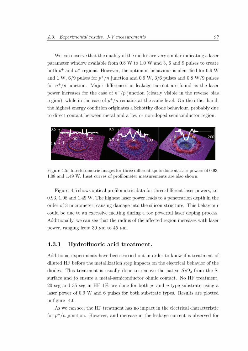
4.3. Experimental results. J-V measurements 97
We can observe that the quality of the diodes are very similar indicating a laser
parameter window available from 0.8 W to 1.0 W and 3, 6 and 9 pulses to create
both p+ and n+ regions. However, the optimum behaviour is identified for 0.9 W
and 1 W, 6/9 pulses for p+/n junction and 0.9 W, 3/6 pulses and 0.8 W/9 pulses
for n+/p junction. Major differences in leakage current are found as the laser
power increases for the case of n+/p junction (clearly visible in the reverse bias
region), while in the case of p+/n remains at the same level. On the other hand,
the highest energy condition originates a Schottky diode behaviour, probably due
to direct contact between metal and a low or non-doped semiconductor region.
Figure 4.5: Interferometric images for three different spots done at laser powers of 0.93,1.08 and 1.49 W. Inset curves of profilometer measurements are also shown.
Figure 4.5 shows optical profilometric data for three different laser powers, i.e.
0.93, 1.08 and 1.49 W. The highest laser power leads to a penetration depth in the
order of 3 micrometer, causing damage into the silicon structure. This behaviour
could be due to an excessive melting during a too powerful laser doping process.
Additionally, we can see that the radius of the affected region increases with laser
power, ranging from 30 µm to 45 µm.
4.3.1 Hydrofluoric acid treatment.
Additional experiments have been carried out in order to know if a treatment of
diluted HF before the metallization step impacts on the electrical behavior of the
diodes. This treatment is usually done to remove the native SiO2 from the Si
surface and to ensure a metal-semiconductor ohmic contact. No HF treatment,
20 seg and 35 seg in HF 1% are done for both p- and n-type substrate using a
laser power of 0.9 W and 6 pulses for both substrate types. Results are plotted
in figure 4.6.
As we can see, the HF treatment has no impact in the electrical characteristic
for p+/n junction. However, and increase in the leakage current is observed for

98Chapter 4. Emitter formation using laser doping technique on n- and p-type
c-Si substrates
1E-08
1E-07
1E-06
1E-05
1E-04
1E-03
1E-02
1E-01
1E+00
1E+01
-1 -0.5 0 0.5 1
Curr
ent
density,
J (
A/c
m2)
Voltage (V)
Without HF treatment
20 seg. HF treatment
35 seg. HF treatment
(a) p+/n junction. 6 Pulses mode
1E-08
1E-07
1E-06
1E-05
1E-04
1E-03
1E-02
1E-01
1E+00
1E+01
-1 -0.5 0 0.5 1
Voltage
Without HF treatment
20 seg. HF treatment
35 seg. HF treatment
(b) n+/p junction. 6 Pulses mode
Figure 4.6: Dark J-V characteristics of p+/n (left) and n+/p junction (right). No HFtreatment, HF 1% for 20 s and 35 s are done before metallization process.
n+/p junction when a HF treatment is done. In our opinion, this behaviour is
related to pinholes in the a−SiCx (n)stack/a−SiCx where the native oxide is re-
moved by the HF treatment and the subsequent metallization results in shunting
paths. Notice that more than 90% of device area consists of a metal layer over an
insulator film and any absence of it allows the metal to directly contact the c-Si
substrate. This effect is strongly reduced in Al2O3/a−SiCx stack since the Al2O3
layer is deposited by ALD technique that lead to a much less pin-hole density in
the films compared to PECVD one.
In all cases the dark J-V curves flatten at high voltage mainly due to ohmic
losses hindering the characterization of the exponential current mechanism. In
order to evaluate the quality of this exponential trend, we measure the best p+/n
and n+/p diode at different temperatures in the 298-363 K range.
J-V curves are fitted using the following two diode expression (4.1) and taking
into account that series resistance rs does not vary with temperature or applied
voltage:
J(V ) = Jo1(eA(V −J(V )rs − 1) + Jo2eA(V −J(V )rs − 1 +
V − J(V )rs
rsh(4.1)

4.3. Experimental results. J-V measurements 99
where for every exponential trend Jo is the saturation current density, A
(A = q/nKT ) is an exponential factor and n is the ideality factor respectively.
From the dependence of A and the corresponding Jo on the temperature, the
carrier transport mechanism behind the exponential trend can be identified.
A summary of the basic conduction mechanisms is given in table 4.1.
Transport mechanisms Jo A n
Diffusion Jo ∝ exp(−Eg/KT ) q/nKT n = 1
Recombination Jo ∝ exp(−Eg/2KT ) q/nKT 1 < n 6 2
Tunneling Jo ∝ exp(−Eac/KT ) const. n 6= const.
Thermionic Jo ∝ exp(−ϕB/KT )KT 3/2 q/KT n = 1
Table 4.1: Basic transport mechanisms. Eg is the energy gap, K is the Boltzmannconstant, T is the absolute temperature, n the ideality factor, Eac is the activationenergy, and ϕB is the barrier energy.
Applying the electrical model and assuming an ideality factor of one for the
main current mechanism related to the first exponential dependence in equation
4.1 (n = 1), Jo1 can be extracted at different temperatures. All these data can be
arranged in an Arrhenius plot where the logarithm of Jo1 is plotted as a function
of the inverse of the temperature. In this type of plots, a straight line is expected
for current mechanism thermally activated and their activation energy can be
extracted from the line slope. As it is shown in figure 4.7 the Arrehnius plot
reveals an activation energy of 1.1 eV corresponding to the silicon bandgap. This
result together with the ideality factor of 1 indicates that current is controlled
by minority carrier recombination at the quasi-neutral c-Si bulk. Additionally,
we can conclude that recombination at the space charge region and thus crystal
damage is not dominant in the device performance.
Due to the high quality of the laser doped regions and the surface passivation
provided by dielectric films, this technique is well suited to c-Si solar cells. Figure
4.8 shows dark J-V measurements and the resulting theoretical curves once the
influence rs has been canceled in order to a correct estimation of Voc from the
dark J-V curve (the normalized series resistance considering the diode area is 0.15
Ωcm2 in both cases). As it can be observed, assuming a photogenerated current

100Chapter 4. Emitter formation using laser doping technique on n- and p-type
c-Si substrates
density of 36 mA/cm2 at 1 sun-illumination, a Voc about 0.63 V and 0.64 V are
expected for p+/n and n+/p junctions respectively. These values are promising
results and can be considered in the state of the art of commercial c-Si solar cells.
Figure 4.7: Arrehnius plot of the Jo1 against 1/KT. Dark J-V measurements at differenttemperatures are done for p+/n and n+/p junction formed at 0.9 W, 6 pulses andwithout HF treatment. The exponential gives activation energy of 1.1 eV correspondingto the silicon Egap.
1E-04
1E-03
1E-02
1E-01
1E+00
1E+01
0.4 0.5 0.6 0.7 0.8 0.9 1
Cu
rren
t Den
sity
, J (
A.c
m-2
)
Voltage (V)
J-V measurements at 25 ºC
Fitting two-diode model
Voc = 0.630V
(expected)
J = 37 mA/cm2
rs Influence
!0.15 ".cm2
n = 1
(a) p+/n junction.
1E-04
1E-03
1E-02
1E-01
1E+00
1E+01
0.4 0.5 0.6 0.7 0.8 0.9 1
Cu
rren
t Den
sity
, J (
A.c
m-2
)
Voltage (V)
J-V measurements at 25 ºC
Fitting two-diode model
Voc = 0.645V
(expected)
J = 36 mA/cm2
rs Influence
!0.15 ".cm2
n = 1
(b) n+/p junction.
Figure 4.8: Dark J-V measurements at 25 oC for p+/n (a) and n+/p (b) junctions(symbols). Laser power of 0.9 W (6 pulses) and no HF treatment are considered inboth cases. The two-diode model fitting without rs is displayed in black dashed line.Diffusion diode term considering n = 1 (continuous black line), resulting from thefitting, is also included as a reference.
4.4. Conclusion 101
4.4 Conclusion
In this chapter we have explored different laser conditions, i.e. laser power and
number of laser pulses, to create reliable p+/n and n+/p junctions on c-Si using
Laser doping technique. In this case, dielectric layers (Al2O3 and a − SiCx (n)
stack) were applied as both dopant sources and surface passivation layers. Opti-
mum laser conditions were established studying systematically dark J-V measure-
ments. Excellent quality of the p+ and n+ regions has been formed from 0.8 W to
1 W and 3/6/9 pulses. Additionally, a study of a diluted HF treatment before the
metallization process has been also done concluding that best electrical behavior
corresponds to no HF treatment. Finally, dark J-V measurements for different
temperatures have demonstrated that the main current mechanism is linked to
minority carrier recombination in the quasi-neutral bulk and, thus, that laser
damage is not dominant in device performance. The high quality of the junctions
and the excellent surface passivation makes laser doping technique using dielectric
layers as dopand source suitable for solar cells applications. A promising open
circuit voltages at 1 sun-illumination of about 640 mV are expected for this type
of solar cells.
102 Bibliography
Bibliography
[1] A.W.Y. Ho and Stuart R. Wenham. Buried contact solar cells with innovative
rear localised contacts. Progress in Photovoltaics: Research and Applications,
12:297–308, 2004.
[2] E. Schneiderlöchner, R. Preu, R. Lüdemann, and S. W. Glunz. Laser-fired
rear contacts for crystalline silicon solar cells. Progress in Photovoltaics:
Research and Applications, 10:29–34, 2002.
[3] D. Carrió, P. Ortega, I. Martín, G. López, J. M. López-González, A. Orpella,
C. Voz, and R. Alcubilla. Rear contact pattern optimization based on 3D
Simulations for IBC Solar Cells with Point-like Doped Contacts. Energy
Procedia, 55:47–52, 2014.
[4] I. Martín, P. Ortega, M. Colina, A. Orpella, G. López, and R. Alcubilla.
Laser processing of Al2O3/a−SiCx : H stacks: a feasible solution for the rear
surface of high-efficiency p-type c-si solar cells. Progress in Photovoltaics:
Research and Applications, 21:1171–1175, 2012.
[5] L. Pirozzi, U.B. Vetrella, Mauro Falconieri, and E. Salza. A laser system for
silicon solar cell processing: Design, setup and operation. Materials Science
Forum, 173-174:319–324, 1995.
[6] L Pirozzi, U. Besi-Vetrella, and E. Salza. Innovative applications of laser
technology in photovoltaics. In Proc. SPIE Conf. Laser Applications in Mi-
croelectronic and Optoelectronic Manufacturing II, 1997.
[7] A. Knorz, M. Peters, A. Grohe, C. Harmel, and R. Preu. Selective laser
ablation of SiNx layers on textured surfaces for low temperature front side
metallizations. Progress in Photovoltaics: Research and Applications, 17:
127–136, 2009.
[8] A. Ogane, K. Horiuchi, A. Kitiyanan, Y. Uraoka, and T. Fuyuki. Feasible
control of laser doping profiles in silicon solar cell processing using multiple
excitation wavelengths. In 2008 33rd IEEE Photovolatic Specialists Confer-
ence, pages 1–4. IEEE, 2008.
[9] G. B. Turner. Solar cells made by laser-induced diffusion directly from phos-
phine gas. Applied Physics Letters, 39:967, 1981.

Bibliography 103
[10] D. Kray, A. Fell, S. Hopman, K. Mayer, G. P. Willeke, and S. W. Glunz.
Laser Chemical Processing (LCP). A versatile tool for microstructuring ap-
plications. Applied Physics A, 93:99–103, 2008.
[11] E. Fogarassy. Silicon solar cells realized by laser induced diffusion of vacuum-
deposited dopants. Journal of Applied Physics, 52:1076, 1981.
[12] M. Colina, I. Martín, C. Voz, A. Morales-Vilches, P. Ortega, G. López,
A. Orpella, R. Alcubilla, I. Sánchez-Aniorte, and C. Molpeceres. Optimiza-
tion of laser doping processes for the creation of p+ regions from solid dopand
sources. In 27 th EUPVSEC, pages 1885–1889, 2012.
[13] G. López, P. Ortega, C. Voz, I. Martín, M. Colina, A. Morales-Vilches, A. Or-
pella, and R. Alcubilla. Surface passivation and optical characterization of
Al2O3/a − SiCx stacks on c-Si substrates. Beilstein journal of nanotechnol-
ogy, 4:726–31, 2013.
[14] I. Martín, M. Colina, A. Coll, G. López, P. Ortega, A. Orpella, and R. Al-
cubilla. c-si solar cells based on laser-processed dielectric films. In 4th Inter-
national Conference on Silicon Photovoltaics, Silicon PV. Energy Procedia,
2014.
[15] M. Okanovic, U. Jäger, M. Ahrens, U. Stute, A. Grohe, and R. Preu. Influ-
ence of different laser parameters in laser doping from phosphosilicate glass.
In 24th European PV Solar Energy Conference and Exhibition, EUPVSEC,
Hamburg (Germany), 2009.
[16] A. Fell, E. Franklin, D. Walter, D. Suh, and K. Weber. Laser doping from
Al2O3 layers. In 27th European PV Solar Energy Conference and Exhibition,
EUPVSEC, Frankfurt (Germany), 2012.
[17] Z. Hameiri, L. Mai, T. Puzzer, and S.R. Wenham. Influence of laser power
on the properties of laser doped solar cells. Solar Energy Materials and Solar
Cells, 95:1085–1094, 2011.

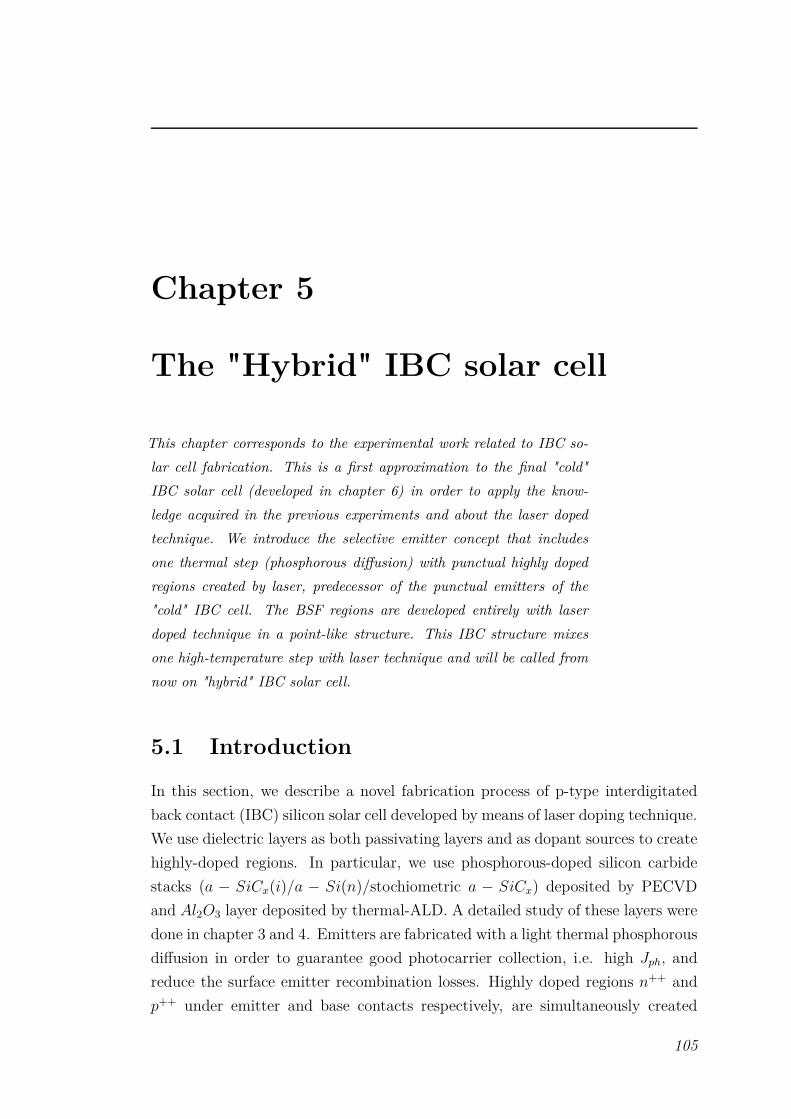
Chapter 5
The "Hybrid" IBC solar cell
This chapter corresponds to the experimental work related to IBC so-
lar cell fabrication. This is a first approximation to the final "cold"
IBC solar cell (developed in chapter 6) in order to apply the know-
ledge acquired in the previous experiments and about the laser doped
technique. We introduce the selective emitter concept that includes
one thermal step (phosphorous diffusion) with punctual highly doped
regions created by laser, predecessor of the punctual emitters of the
"cold" IBC cell. The BSF regions are developed entirely with laser
doped technique in a point-like structure. This IBC structure mixes
one high-temperature step with laser technique and will be called from
now on "hybrid" IBC solar cell.
5.1 Introduction
In this section, we describe a novel fabrication process of p-type interdigitated
back contact (IBC) silicon solar cell developed by means of laser doping technique.
We use dielectric layers as both passivating layers and as dopant sources to create
highly-doped regions. In particular, we use phosphorous-doped silicon carbide
stacks (a − SiCx(i)/a − Si(n)/stochiometric a − SiCx) deposited by PECVD
and Al2O3 layer deposited by thermal-ALD. A detailed study of these layers were
done in chapter 3 and 4. Emitters are fabricated with a light thermal phosphorous
diffusion in order to guarantee good photocarrier collection, i.e. high Jph, and
reduce the surface emitter recombination losses. Highly doped regions n++ and
p++ under emitter and base contacts respectively, are simultaneously created
105
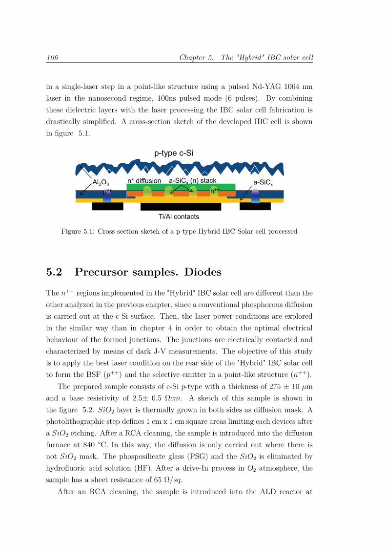
106 Chapter 5. The "Hybrid" IBC solar cell
in a single-laser step in a point-like structure using a pulsed Nd-YAG 1064 nm
laser in the nanosecond regime, 100ns pulsed mode (6 pulses). By combining
these dielectric layers with the laser processing the IBC solar cell fabrication is
drastically simplified. A cross-section sketch of the developed IBC cell is shown
in figure 5.1.
p-type c-Si
n+ diffusion
n++p++
Al2O3
Ti/Al contacts
a-SiCx (n) stack a-SiCx
Figure 5.1: Cross-section sketch of a p-type Hybrid-IBC Solar cell processed
5.2 Precursor samples. Diodes
The n++ regions implemented in the "Hybrid" IBC solar cell are different than the
other analyzed in the previous chapter, since a conventional phosphorous diffusion
is carried out at the c-Si surface. Then, the laser power conditions are explored
in the similar way than in chapter 4 in order to obtain the optimal electrical
behaviour of the formed junctions. The junctions are electrically contacted and
characterized by means of dark J-V measurements. The objective of this study
is to apply the best laser condition on the rear side of the "Hybrid" IBC solar cell
to form the BSF (p++) and the selective emitter in a point-like structure (n++).
The prepared sample consists of c-Si p-type with a thickness of 275 ± 10 µm
and a base resistivity of 2.5± 0.5 Ωcm. A sketch of this sample is shown in
the figure 5.2. SiO2 layer is thermally grown in both sides as diffusion mask. A
photolithographic step defines 1 cm x 1 cm square areas limiting each devices after
a SiO2 etching. After a RCA cleaning, the sample is introduced into the diffusion
furnace at 840 °C. In this way, the diffusion is only carried out where there is
not SiO2 mask. The phosposilicate glass (PSG) and the SiO2 is eliminated by
hydrofluoric acid solution (HF). After a drive-In process in O2 atmosphere, the
sample has a sheet resistance of 65 Ω/sq.
After an RCA cleaning, the sample is introduced into the ALD reactor at
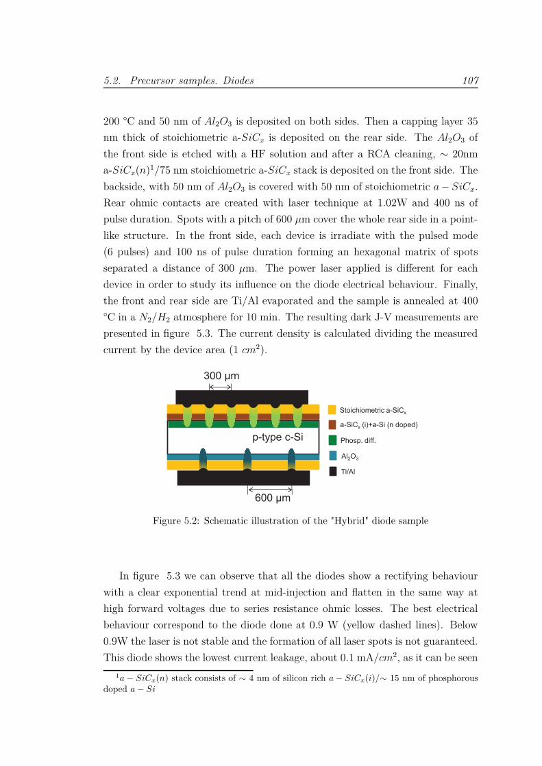
5.2. Precursor samples. Diodes 107
200 °C and 50 nm of Al2O3 is deposited on both sides. Then a capping layer 35
nm thick of stoichiometric a-SiCx is deposited on the rear side. The Al2O3 of
the front side is etched with a HF solution and after a RCA cleaning, ∼ 20nm
a-SiCx(n)1/75 nm stoichiometric a-SiCx stack is deposited on the front side. The
backside, with 50 nm of Al2O3 is covered with 50 nm of stoichiometric a − SiCx.
Rear ohmic contacts are created with laser technique at 1.02W and 400 ns of
pulse duration. Spots with a pitch of 600 µm cover the whole rear side in a point-
like structure. In the front side, each device is irradiate with the pulsed mode
(6 pulses) and 100 ns of pulse duration forming an hexagonal matrix of spots
separated a distance of 300 µm. The power laser applied is different for each
device in order to study its influence on the diode electrical behaviour. Finally,
the front and rear side are Ti/Al evaporated and the sample is annealed at 400
°C in a N2/H2 atmosphere for 10 min. The resulting dark J-V measurements are
presented in figure 5.3. The current density is calculated dividing the measured
current by the device area (1 cm2).
p-type c-Si
Stoichiometric a-SiCx
a-SiCx (i)+a-Si (n doped)
Phosp. diff.
Al2O3
300 µm
600 µm
Ti/Al
Figure 5.2: Schematic illustration of the "Hybrid" diode sample
In figure 5.3 we can observe that all the diodes show a rectifying behaviour
with a clear exponential trend at mid-injection and flatten in the same way at
high forward voltages due to series resistance ohmic losses. The best electrical
behaviour correspond to the diode done at 0.9 W (yellow dashed lines). Below
0.9W the laser is not stable and the formation of all laser spots is not guaranteed.
This diode shows the lowest current leakage, about 0.1 mA/cm2, as it can be seen
1a − SiCx(n) stack consists of ∼ 4 nm of silicon rich a − SiCx(i)/∼ 15 nm of phosphorousdoped a − Si

108 Chapter 5. The "Hybrid" IBC solar cell
Cu
rren
t d
ensi
ty J
[A
/cm
2]
Voltage [V]
Figure 5.3: Dark J-V measurements of the "Hybrid" diodes at different laser powers
in the reverse bias region as a consequence of the highest rshunt. The rshunt is
clearly affected by the laser power. As the laser power increases the rshunt de-
creases deteriorating the J-V diode response. In the forward bias the exponential
trend of the diffusion diode is clearly hidden by the influence of rshunt (being
predominant at 1.24 W).
5.3 Emitter saturation current (Joe) study
In the "Hybrid" IBC solar cell, we have to distinguish between three different
interfaces in order to study the surface passivation properties, i.e. the front tex-
tured surface covered with 90 nm of Al2O3, the polished rear base region covered
with 90 nm of Al2O3 as passivating layer and covered with 35 nm of stoichio-
metric a-SiCx and the polished emitter region thermally phosphorous doped and
covered with a-Si(n) stack + 75 nm stoichiometric a − SiCx. The latter will be
the focus of the next passivation study. The other two passivated interfaces were
previously studied in detail in chapter 3.
The sample under study consists of a p-type c-Si with a thickness of 275 ± 10
µm and a base resistivity of 2.5± 0.5 Ωcm. The sample is cleaned with the RCA

5.3. Emitter saturation current (Joe) study 109
sequence before a phosphorous diffusion performed at 840°C. The phosphosilicate
glass grown is etched with HF solution. Then, the sample is again cleaned with
RCA and submitted to a thermal drive-in in O2 atmosphere, achieving a final
sheet resistance of ∼ 65 Ω/sq. The SiO2 is etched and the sample is introduced
in the PECVD chamber to deposit on both sides a a − SiCx(n) stack/75 nm
stoichometric a − SiCx.
Emitter saturation current (Joe) is determined measuring effective lifetime on
the symmetrical c-Si sample processed. Test structure n+pn+ is shown in figure
5.4a. The carrier lifetime is measured before laser processing. Then, we irradiate
only one surface with laser spots with a pitch of 250 µm covering 4.5% of the
total surface area and τeff is measured again. Joe is extracted from the slope of
the 1/τeff vs. ∆n at high injection levels using the method proposed by Kane
and Swanson [1] (see Fig. 5.4b). Emitter saturation currents of 36 fA/cm2 and 42
fA/cm2 are obtained before and after laser stage respectively. Therefore a Joe can
be deduced for each selective emitter point yielding ∼150 fA/cm2. Despite the
Joe does not change much before and after laser process, there is a degradation
of the bulk lifetime as it can be deduced from the shift between the curves. This
deterioration has probably been caused by the damage into the bulk lattice during
the laser doping stage.
Laser emitter p-type c-Si
Ph. difussion
a-SiCx (n) stack +a-SiCx
(a)
1/
eff [s
-1]
Excess carrier density [cm-3]
(b)
Figure 5.4: (a) Symmetrical test structure for measurements of minority carrier life-time. (b) Determination of Joe using the "slope method" for a symmetrical samplebefore (round-shaped) and after laser process (square-shaped) when a point-like selec-tive emitters are created
110 Chapter 5. The "Hybrid" IBC solar cell
5.4 "Hybrid" IBC Fabrication process
As starting material, we use p-type float-zone (FZ) silicon wafers with a thickness
of 275 ± 10 µm and a base resistivity of 2.5± 0.5 Ωcm (the same substrate used
in previous experimental). In figure 5.5 is described step by step the "hybrid"
IBC cell fabrication process.
(1) The fabrication starts with a RCA cleaning and a light thermal diffusion
performed at 840 °C from solid source. The phosphorous glass grown is etched
with HF (5%) Dip.
(2) A subsequent O2 drive-in (1080°) after an RCA cleaning results in a grow of
a SiO2 layer and in a n+ emitter with 65 Ω/sq sheet resistance.
(3) The SiO2 of the front layer is etched side with a commercial SiO2 etching
solution.
(4) The SiO2 of the backside is used to protect the surface from the subse-
quent front side random texturation achieved by tetramethyl ammonium hydrox-
ide (TMAH) solution. The front side is textured at the same time that the
phosphorous diffusion is etched.
(5) and (6) After removing the back SiO2 mask layer, we deposit on the whole
rear side by PECVD a dielectric a − SiCx (n) stack and 25 nm stoichiometric
a − SiCx for chemical protection purposes.
(7) and (8) Emitter regions are defined through standard photolithography follo-
wed by plasma dry etching (CF4) to remove the stoichiometric a − SiCx and the
a − SiCx(n) stack from the undesired areas. A subsequent isotropic etching re-
moves the c-Si phosphorous doped from the base regions. This isotropic etching
consist of 200 ml HNO3 + 8 ml HF (50%)+ 200 ml H2O(DI) for 4 minutes.
(9) The photoresist is stripped and after a RCA cleaning, we deposit 90 nm of
Al2O3 by thermal-ALD at 200 °C on both sides. This layer plays the role of
passivating front and rear base surface , antireflection coating and as aluminium
source for a later BSF formation (p++).
(10) and (11) Base regions are defined by photolithography and the Al2O3 is wet
etched from the emitter regions.
(12) After removing the photoresist, an additional stoichiometric a − SiCx film
(50 nm thick) is deposited on the whole device rear side to optimize the back
reflector and improve the laser process.
(13) Next, the rear of the solar cells are laser irradiated in one single laser step
applying 6 pulses per spot (laser pulse duration of 100 ns) in a point-like square
5.4. "Hybrid" IBC Fabrication process 111
matrix arrangement with a pitch of 250 µm. In this way, laser beam simultane-
ously ablates the dielectric layers and diffuses the dopant atoms creating highly
doped n++ (selective emitter) and p++ (BSF) regions. These highly doped re-
gions underneath the contacts helps for the formation of a good ohmic contact.
0.9 W is the laser power selected considering the results obtained in the study of
the precursor p++/n done in the chapter 4 and diffused n++/p in section 5.2 of
this chapter.
(14) Just after the laser stage, the rear side is totally covered by e-beam evapo-
rated Ti/Al film stack.
(15) and (16) A photolithographic step and Ti and Al wet etching define both
emitter and base metal contacts in an interdigitated pattern.
(17) Finally, an annealing at 400 °C for 10 min in H2/N2 atmosphere recovers
the damage produced during the e-beam evaporation and activates the negative
charge in the Al2O3/c-Si interface.
The illuminated area on the front side is defined using an extra aluminium
thermal evaporation on the front surface. This aluminium layer is properly patter-
ned and aligned face to face with the rear side (electrode side) to act as a shadow
mask defining light windows of 3 cm x 3 cm (the busbar is not take into account).
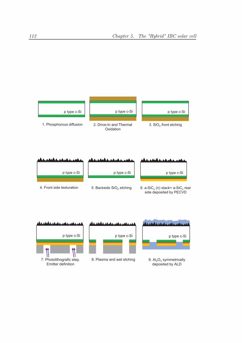
112 Chapter 5. The "Hybrid" IBC solar cell

5.4. "Hybrid" IBC Fabrication process 113
Figure 5.5: Schematic illustration of Hybrid IBC fabrication process
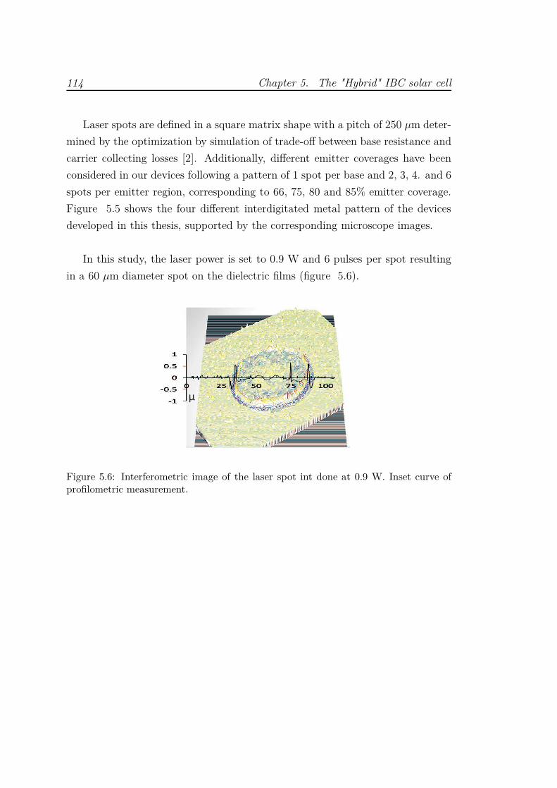
114 Chapter 5. The "Hybrid" IBC solar cell
Laser spots are defined in a square matrix shape with a pitch of 250 µm deter-
mined by the optimization by simulation of trade-off between base resistance and
carrier collecting losses [2]. Additionally, different emitter coverages have been
considered in our devices following a pattern of 1 spot per base and 2, 3, 4. and 6
spots per emitter region, corresponding to 66, 75, 80 and 85% emitter coverage.
Figure 5.5 shows the four different interdigitated metal pattern of the devices
developed in this thesis, supported by the corresponding microscope images.
In this study, the laser power is set to 0.9 W and 6 pulses per spot resulting
in a 60 µm diameter spot on the dielectric films (figure 5.6).
µ
Figure 5.6: Interferometric image of the laser spot int done at 0.9 W. Inset curve ofprofilometric measurement.

5.4. "Hybrid" IBC Fabrication process 115
Figure 5.7: Rear interdigitated metal pattern. From top to bottom 66, 75, 80 and 85%emitter coverage. In the right side the corresponding microscopes images.
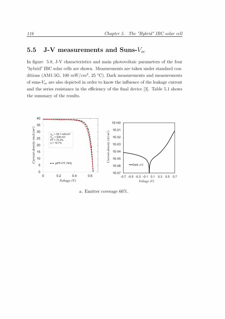
116 Chapter 5. The "Hybrid" IBC solar cell
5.5 J-V measurements and Suns-Voc
In figure 5.8, J-V characteristics and main photovoltaic parameters of the four
"hybrid" IBC solar cells are shown. Measurements are taken under standard con-
ditions (AM1.5G, 100 mW/cm2, 25 °C). Dark measurements and measurements
of suns-Voc are also depicted in order to know the influence of the leakage current
and the series resistance in the efficiency of the final device [3]. Table 5.1 shows
the summary of the results.
Cu
rren
t d
ensi
ty (
mA
/cm
2)
Voltage (V)
Cu
rren
t d
ensi
ty (
A/c
m2)
Voltage (V)
a. Emitter coverage 66%.
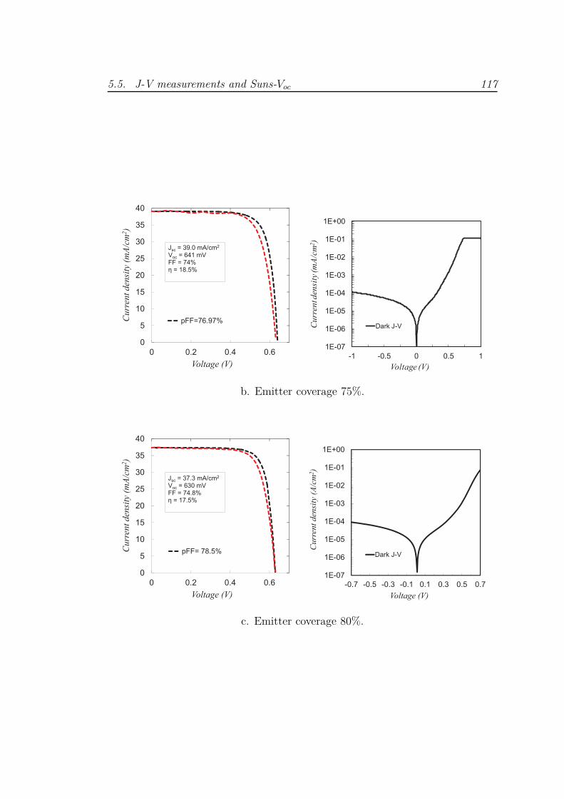
5.5. J-V measurements and Suns-Voc 117
Cu
rren
t d
ensi
ty (
mA
/cm
2)
Voltage (V)
1E-07
1E-06
1E-05
1E-04
1E-03
1E-02
1E-01
1E+00
-1 -0.5 0 0.5 1
Cu
rren
t den
sity
(m
A/c
m2)
Voltage (V)
Dark J-V
b. Emitter coverage 75%.
Cu
rren
t d
ensi
ty (
mA
/cm
2)
Voltage (V)
Cu
rren
t d
ensi
ty (
A/c
m2)
Voltage (V)
c. Emitter coverage 80%.
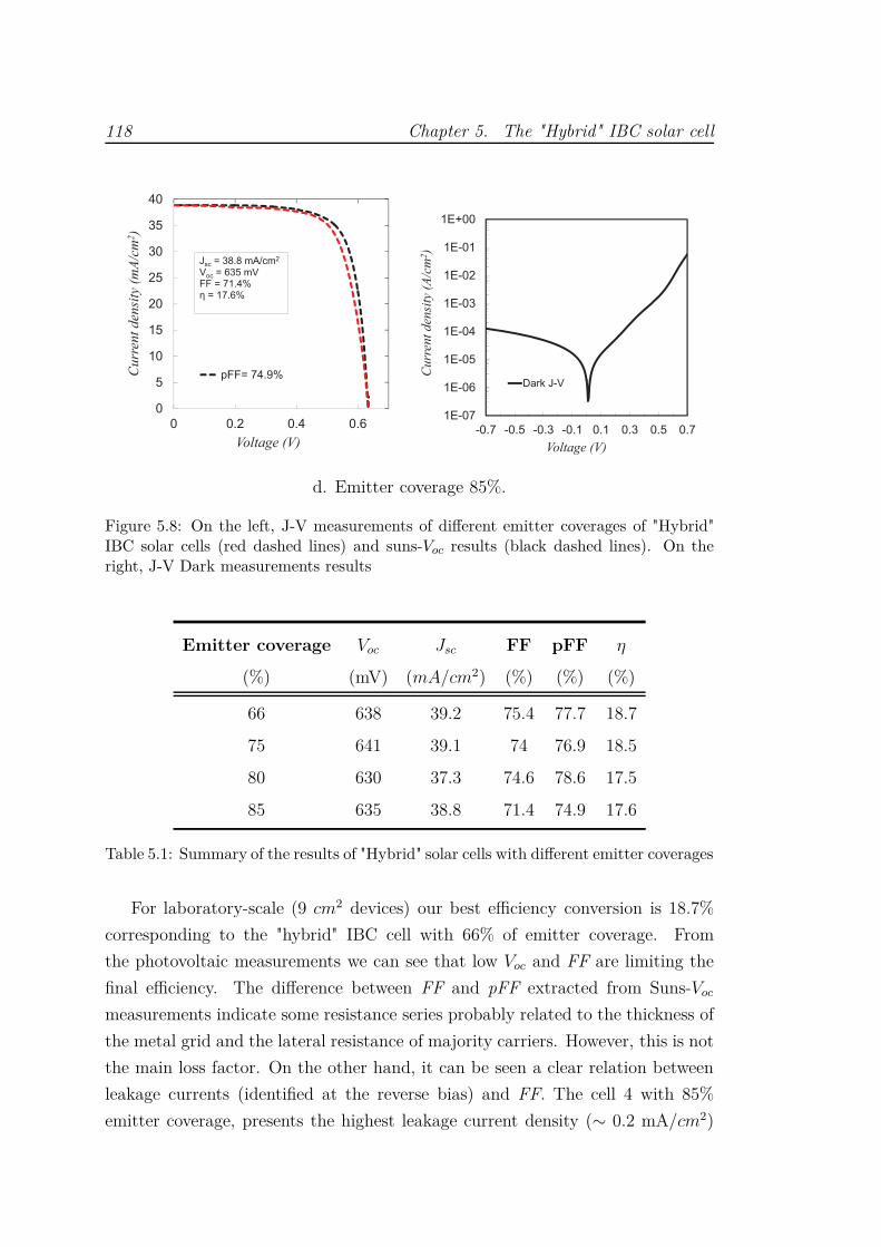
118 Chapter 5. The "Hybrid" IBC solar cellC
urr
ent
den
sity
(m
A/c
m2)
Voltage (V)
Cu
rren
t d
ensi
ty (
A/c
m2)
Voltage (V)
d. Emitter coverage 85%.
Figure 5.8: On the left, J-V measurements of different emitter coverages of "Hybrid"IBC solar cells (red dashed lines) and suns-Voc results (black dashed lines). On theright, J-V Dark measurements results
Emitter coverage Voc Jsc FF pFF η
(%) (mV) (mA/cm2) (%) (%) (%)
66 638 39.2 75.4 77.7 18.7
75 641 39.1 74 76.9 18.5
80 630 37.3 74.6 78.6 17.5
85 635 38.8 71.4 74.9 17.6
Table 5.1: Summary of the results of "Hybrid" solar cells with different emitter coverages
For laboratory-scale (9 cm2 devices) our best efficiency conversion is 18.7%
corresponding to the "hybrid" IBC cell with 66% of emitter coverage. From
the photovoltaic measurements we can see that low Voc and FF are limiting the
final efficiency. The difference between FF and pFF extracted from Suns-Voc
measurements indicate some resistance series probably related to the thickness of
the metal grid and the lateral resistance of majority carriers. However, this is not
the main loss factor. On the other hand, it can be seen a clear relation between
leakage currents (identified at the reverse bias) and FF. The cell 4 with 85%
emitter coverage, presents the highest leakage current density (∼ 0.2 mA/cm2)
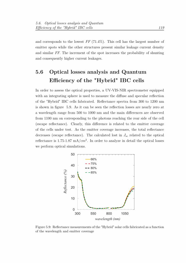
5.6. Optical losses analysis and QuantumEfficiency of the "Hybrid" IBC cells 119
and corresponds to the lowest FF (71.4%). This cell has the largest number of
emitter spots while the other structures present similar leakage current density
and similar FF. The increment of the spot increases the probability of shunting
and consequently higher current leakages.
5.6 Optical losses analysis and Quantum
Efficiency of the "Hybrid" IBC cells
In order to assess the optical properties, a UV-VIS-NIR spectrometer equipped
with an integrating sphere is used to measure the diffuse and specular reflection
of the "Hybrid" IBC cells fabricated. Reflectance spectra from 300 to 1200 nm
is shown in figure 5.9. As it can be seen the reflection losses are nearly zero at
a wavelength range from 500 to 1000 nm and the main differences are observed
from 1100 nm on corresponding to the photons reaching the rear side of the cell
(escape reflectance). Clearly, this difference is related to the emitter coverage
of the cells under test. As the emitter coverage increases, the total reflectance
decreases (escape reflectance). The calculated lost in Jsc related to the optical
reflectance is 1.75-1.87 mA/cm2. In order to analyze in detail the optical losses
we perform optical simulations.
Ref
lect
ance
(%
)
wavelength (nm)
Figure 5.9: Reflectance measurements of the "Hybrid" solar cells fabricated as a functionof the wavelength and emitter coverage

120 Chapter 5. The "Hybrid" IBC solar cell
5.6.1 Simulation of the solar cell optics
In order to analyze the optical losses, optical simulations are done using the wafer
ray tracer tool of PV Lighthouse (https://www.pvlighthouse.com.au). The resul-
ting simulation spectra reflectance, absorbance and transmitance are depicted in
figure 5.11 as a function of the three different regions involved in the rear side of
the "hybrid" IBC cell. Figure 5.10 shows a sketch of the structure for the optical
simulations. The front side is considered randomly textured and coated with 90
nm of Al2O3. An extrapolated study according to the different IBC structures
fabricated and taking into account the percentage of each contribution region as
a function of the emitter coverage (see figure 5.7) is also done. The results are
shown is the table 5.2 and 5.3 where the Jsc reduction due to optical losses are
shown.
c-Si p-type 1 2 3
Figure 5.10: Simplified sketch of the "Hydrid" IBC solar cell rear side for optical simu-lations
• 1. Metallized base region:
c-Si+90 nm Al2O3+50 nm stoichiometric a − SiCx+Ti+Al
• 2. Metallized emitter region:
c-Si+∼20 nm a-Si(n) stack 2+75 nm stoichiometric a − SiCx
+Ti+Al
• 3.Non-metallized region:
c-Si+∼20 nm a-Si(n) stack +25 nm stoichiometric a − SiCx+90 nm Al2O3
+50 nm stoichiometric a − SiCx
2a − SiCx(n) stack consists of ∼ 4 nm of silicon rich a − SiCx(i)/∼ 15 nm of phosphorousdoped a − Si
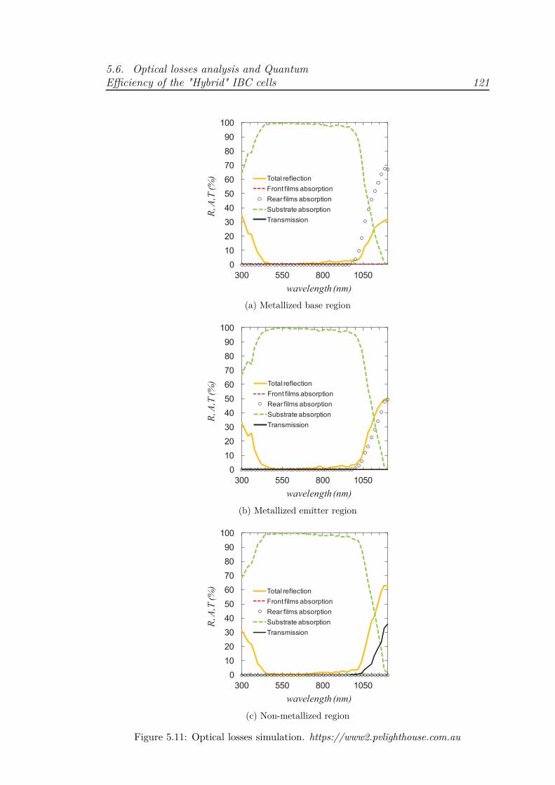
5.6. Optical losses analysis and QuantumEfficiency of the "Hybrid" IBC cells 121
0
10
20
30
40
50
60
70
80
90
100
300 550 800 1050
R, A
,T (
%)
wavelength (nm)
Total reflection
Front films absorption
Rear films absorption
Substrate absorption
Transmission
(a) Metallized base region
0
10
20
30
40
50
60
70
80
90
100
300 550 800 1050
R, A
,T (
%)
wavelength (nm)
Total reflection
Front films absorption
Rear films absorption
Substrate absorption
Transmission
(b) Metallized emitter region
0
10
20
30
40
50
60
70
80
90
100
300 550 800 1050
R, A
,T (
%)
wavelength (nm)
Total reflection
Front films absorption
Rear films absorption
Substrate absorption
Transmission
(c) Non-metallized region
Figure 5.11: Optical losses simulation. https://www2.pvlighthouse.com.au

122 Chapter 5. The "Hybrid" IBC solar cell
Optical losses [mA/cm2]
E. cover. Distrib. Reflec. Absorp. Trans.
[%] Emitter [%] Ext. Esc. Front Rear
Base[%]
Non-metal.[%]
50.1 0.51 0.52 2.53.10−15 1.55 -
66 29.5 0.32 0.52 1.63.10−15 0.49 -
20.4 0.20 0.44 1.23.10−15 3.88.10−16 0.17
63.7 0.65 0.66 3.21.10−15 1.96 -
75 23.7 0.25 0.41 1.31.10−15 0.39 -
12.6 0.12 0.27 7.59.10−16 2.40.10−16 0.11
68 0.69 0.71 3.43.10−15 2.10 -
80 20 0.21 0.35 1.10.10−15 0.33 -
12 0.12 0.26 7.23.10−16 2.28.10−16 0.10
79.6 0.81 0.83 4.02.10−15 2.46 -
85 16.8 0.18 0.29 9.29.10−16 0.28 -
3.6 0.03 0.08 2.17.10−16 6.86.10−17 0.03
Table 5.2: Optical losses distribution depending on the rear IBC region and emittercoverage
IBC structure Reflectance Absorption Transmitance Total loss Photogen. (Absorbed)
% coverage [mA/cm2] [mA/cm2] [mA/cm2] [mA/cm2] [mA/cm2]
66 2.51 2.04 0.17 4.72 41.49
75 2.36 2.35 0.11 4.82 41.37
80 2.34 2.43 0.10 4.87 41.34
85 2.22 2.74 0.03 4.99 41.22
Table 5.3: Optical losses distribution depending of rear IBC region and emitter coverage

5.6. Optical losses analysis and QuantumEfficiency of the "Hybrid" IBC cells 123
Major reduction of the optical losses is due to the absence of the front side
metallization grid and an adequate design of the front surface texturation and
antireflection coating. However, there are still other remaining optical losses
that jeopardize the current generation of the solar cell. As it can be seen in
graphs (figure 5.11) the largest loss mechanism is the surface reflectance (external
and escape) which accounts more than 50% of the total optical losses. The
former is caused by non-optimal properties of the antireflection coating, the latter
is a result of non-ideal light-trapping, where light rays are reflected out of the
cell after multiple internal reflections. As it was obtained in the experimental
reflectance, there is a trend in the total reflectance whose value decreases as the
emitter coverage increases. The parasitic absorption of the rear films (mainly Ti)
participates in an important manner while the transmission losses are considerable
in the region without metal.
Taken into account each percentage of the region involved for the different
structures and the simulated results (see table 5.2 and 5.3), we can deduce
that the non-metallized region is the main responsible of the small difference in
the reflectance results. From the optical simulation, it can be seen that escape
reflectance loss has a significant weight in the non-metallized region (more than
the emitter and base region) and as the size of this region increases, the escape
reflectance loss also increases. In other words, as the emitter coverage increases,
the non-metallized area decreases and the total reflectance decreases. This result
agrees with the experimental reflectance. On the other hand, the losses due to
the the rear film absorption and transmitance in the metallized base and non-
metallized regions respectively are also very important and then, as the emitter
coverage increases the losses due to the rear film absorption and transmitance
respectively also decreases.
5.6.2 External quantum efficiency analysis
Figure 5.12a shows the external quantum efficiency EQE values as a function
of wavelength of the four IBC structures. Experimental reflectance and internal
quantum efficiency (IQE) calculated as IQE = EQE/(1−R) of our best "Hybrid"
IBC (66% emitter coverage) are also depicted in figure 5.12b.

124 Chapter 5. The "Hybrid" IBC solar cell
EQ
Es(
%)
wavelength (nm)
(a)
0
10
20
30
40
50
60
70
80
90
100
300 550 800 1050
Ref
lect
an
ce (%
)
EQ
Es,
IQ
E(%
)
wavelength (nm)
EQE
Reflectance
IQE Calculed
(b)
Figure 5.12: (a) EQEs measurements of the four different "Hybrid" IBC structures(b) EQE, IQE and Reflectance measurements of the "Hybrid" IBC with 66% emittercoverage
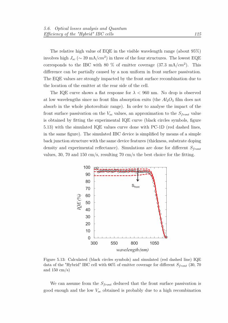
5.6. Optical losses analysis and QuantumEfficiency of the "Hybrid" IBC cells 125
The relative high value of EQE in the visible wavelength range (about 95%)
involves high Jsc (∼ 39 mA/cm2) in three of the four structures. The lowest EQE
corresponds to the IBC with 80 % of emitter coverage (37.3 mA/cm2). This
difference can be partially caused by a non uniform in front surface passivation.
The EQE values are strongly impacted by the front surface recombination due to
the location of the emitter at the rear side of the cell.
The IQE curve shows a flat response for λ < 960 nm. No drop is observed
at low wavelengths since no front film absorption exits (the Al2O3 film does not
absorb in the whole photovoltaic range). In order to analyse the impact of the
front surface passivation on the Voc values, an approximation to the Sfront value
is obtained by fitting the experimental IQE curve (black circles symbols, figure
5.13) with the simulated IQE values curve done with PC-1D (red dashed lines,
in the same figure). The simulated IBC device is simplified by means of a simple
back junction structure with the same device features (thickness, substrate doping
density and experimental reflectance). Simulations are done for different Sfront
values, 30, 70 and 150 cm/s, resulting 70 cm/s the best choice for the fitting.
0
10
20
30
40
50
60
70
80
90
100
300 550 800 1050
IQE
(%
)
wavelength (nm)
Sfront
Figure 5.13: Calculated (black circles symbols) and simulated (red dashed line) IQEdata of the "Hybrid" IBC cell with 66% of emitter coverage for different Sfront (30, 70and 150 cm/s)
We can assume from the Sfront deduced that the front surface passivation is
good enough and the low Voc obtained is probably due to a high recombination
126 Chapter 5. The "Hybrid" IBC solar cell
at the rear side. Once the possible influence of a poor passivated front side is
eliminated, we are going to focus on the analysis to the rear side of the cells.
The most likely explanation for the low Voc is related the laser-induced crystal
damage which can be responsible for limiting the performance of the laser-doped
emitter. If the pulse energy is too high, the surface starts being ablated and
can introduce damage to the silicon lattice. [4]. These defects are recombination
centers locally affecting minority carrier lifetim [5]. On the other hand, during
the laser stage, fluctuations in the power laser have been observed and it could be
the main cause of having deeper and bigger laser spots than expected resulting
in higher lattice damage. This damage strongly increases the recombination rate
in the emitter regions.
Furthermore, the final annealing of the devices done at 400 °C to activate the
Al2O3 passivation can degrade the a-Si(i) increasing the recombination rate at
the emitter regions.
Finally, in order to know if the diode ideality factor (n) plays an special role in
the final FF, we calculate its value using the experimental dark J-V measurements
of the Cell 1 as follow.
n =J
Vt.dJ
dV
(5.1)
We obtain an ideality factor of 1.7 at the maximum power point (see figure
5.14). This value, far away from 1, could be due to either carrier recombination in
the space charge region by the laser damage on the crystal lattice or the influence
of partial shunting generated during the laser stage. These effects are stronger as
the density of laser spots increases in the emitter region.

5.7. Conclusion 127
Idea
lity
fa
cto
r, n
Voltage [V]
V
Figure 5.14: Ideality factor of cell 1 as a function of voltage
5.7 Conclusion
In this chapter, a "hybrid" IBC solar cell on p-type substrate has been developed.
It was fabricated with laser technology through dielectric layers in a point-like
structure for selective emitters and BSF contacts formation. Devices were arran-
ged in four different emitter coverages of 66, 75, 80 and 85%. The selective
emitters include an additional thermal phosphorous diffusion step.
The main photocurrent (Jph) loss mechanism is related to a non-ideal front
surface passivation (70 cm/s). Furthermore, optical simulation points out to extra
Jph losses as a consequence of the back reflector scheme and rear films absorption.
Additionally, the low FF and Voc values are also limiting efficiency. Comparing
pFF and FF it can be deduced that series resistance is not the main cause for
these low values. The relatively high experimental and simulated IQE values
demonstrate that the front surface passivation is good enough for not limiting the
Voc. Consequently, this parameter is affected by both rear surface recombination
and technological issues related to laser processing (parasitic shunting and crystal
lattice damage).

128 Chapter 5. The "Hybrid" IBC solar cell
As a conclusion, better control of the power laser is needed in order to limit
the laser damage in the c-Si lattice. The pulsed mode seems to be more sensitive
to instabilities causing fluctuation in the power laser and to increase the pulse
duration could be a good alternative to improve the laser stage minimizing the
lattice damage. Additionally, the emitter pattern could be modified decreasing
the number of spots. That latest suggestion would decrease Joe and would improve
the Voc.
Bibliography 129
Bibliography
[1] D.E Kane and R.M Swanson. Measurement of the emitter saturation cur-
rent by a contactless photoconductivity decay method. In 18th Photovoltaic
Specialists Conference. IEEE, pages 578–583. IEEE, 1985.
[2] D. Carrió, P. Ortega, I. Martín, G. López, J. M. López-González, A. Or-
pella, C. Voz, and R. Alcubilla. Rear Contact Pattern Optimization based on
3D Simulations for IBC Solar Cells with Point-like Doped Contacts. Energy
Procedia, 55:47–52, 2014.
[3] D. Pysch, A. Mette, and S.W. Glunz. A review and comparison of differ-
ent methods to determine the series resistance of solar cells. Solar Energy
Materials and Solar Cells, 91:1698–1706, 2007.
[4] M. Okanovic, U. Jäger, M. Ahrens, U. Stute, A. Grohe, and R. Preu. Influence
of different laser parameters in laser doping from phosphosilicate glass. In 24th
European PV Solar Energy Conference and Exhibition, EUPVSEC, Hamburg
(Germany), 2009.
[5] M. Abbott, P. Cousins, F. Chen, and J. Cotter. Laser-induced defects in
crystalline silicon solar cells. In 31st IEEE Photovoltaic Specialists Conference
(PVSC), Orlando, pages 1241–1244. IEEE, 2005.


Chapter 6
"Cold" Back-contact
Back-junction silicon solar cells
The application of the knowledge acquired in previous chapters is the
starting point to develop an innovative fabrication process of n-type
interdigitated back-contact (IBC) back-junction c-Si solar cells. The
main feature is that all the highly-doped regions in the cell have been
entirely fabricated through laser processing of dielectric layers, avoi-
ding the high temperature step of the conventional diffusion processes.
Combining dielectric layers as both dopant source and passivating
layer with laser doping technique drastically simplifies the fabrication
process reducing the global thermal budget. Additionally, we have re-
duced the fabrication process to only two patterning steps. The sim-
plicity of the fabrication process proposed in this chapter significantly
reduce time and energy consumption. As a proof of concept, our first
"cold" IBC cells have been developed and characterized.
6.1 Introduction
In the first part of this chapter we analyse the minority diffusion length of the
samples involved and, as in the same way than in "Hybrid" IBC of the previous
chapter, the sheet resistance, the dark J-V measurements of the new precursor
diodes to study the dark electrical characteristic at different laser conditions and
the optical properties. Due to the power fluctuations detected in the experimen-
tal done in chapter 5 and the lattice damage induced into the c-Si structure, two
131
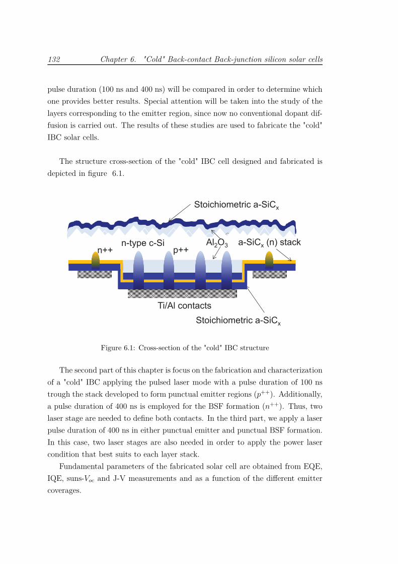
132 Chapter 6. "Cold" Back-contact Back-junction silicon solar cells
pulse duration (100 ns and 400 ns) will be compared in order to determine which
one provides better results. Special attention will be taken into the study of the
layers corresponding to the emitter region, since now no conventional dopant dif-
fusion is carried out. The results of these studies are used to fabricate the "cold"
IBC solar cells.
The structure cross-section of the "cold" IBC cell designed and fabricated is
depicted in figure 6.1.
Figure 6.1: Cross-section of the "cold" IBC structure
The second part of this chapter is focus on the fabrication and characterization
of a "cold" IBC applying the pulsed laser mode with a pulse duration of 100 ns
trough the stack developed to form punctual emitter regions (p++). Additionally,
a pulse duration of 400 ns is employed for the BSF formation (n++). Thus, two
laser stage are needed to define both contacts. In the third part, we apply a laser
pulse duration of 400 ns in either punctual emitter and punctual BSF formation.
In this case, two laser stages are also needed in order to apply the power laser
condition that best suits to each layer stack.
Fundamental parameters of the fabricated solar cell are obtained from EQE,
IQE, suns-Voc and J-V measurements and as a function of the different emitter
coverages.
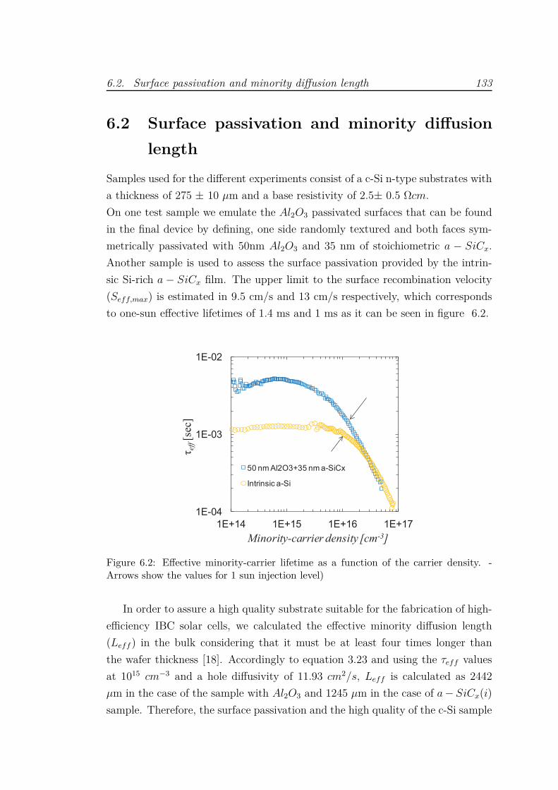
6.2. Surface passivation and minority diffusion length 133
6.2 Surface passivation and minority diffusion
length
Samples used for the different experiments consist of a c-Si n-type substrates with
a thickness of 275 ± 10 µm and a base resistivity of 2.5± 0.5 Ωcm.
On one test sample we emulate the Al2O3 passivated surfaces that can be found
in the final device by defining, one side randomly textured and both faces sym-
metrically passivated with 50nm Al2O3 and 35 nm of stoichiometric a − SiCx.
Another sample is used to assess the surface passivation provided by the intrin-
sic Si-rich a − SiCx film. The upper limit to the surface recombination velocity
(Seff,max) is estimated in 9.5 cm/s and 13 cm/s respectively, which corresponds
to one-sun effective lifetimes of 1.4 ms and 1 ms as it can be seen in figure 6.2.
1E-04
1E-03
1E-02
1E+14 1E+15 1E+16 1E+17
ef
f[s
ec]
Minority-carrier density [cm-3]
50 nm Al2O3+35 nm a-SiCx
Intrinsic a-Si
Figure 6.2: Effective minority-carrier lifetime as a function of the carrier density. -Arrows show the values for 1 sun injection level)
In order to assure a high quality substrate suitable for the fabrication of high-
efficiency IBC solar cells, we calculated the effective minority diffusion length
(Leff ) in the bulk considering that it must be at least four times longer than
the wafer thickness [18]. Accordingly to equation 3.23 and using the τeff values
at 1015 cm−3 and a hole diffusivity of 11.93 cm2/s, Leff is calculated as 2442
µm in the case of the sample with Al2O3 and 1245 µm in the case of a − SiCx(i)
sample. Therefore, the surface passivation and the high quality of the c-Si sample

134 Chapter 6. "Cold" Back-contact Back-junction silicon solar cells
guarantee the conditions for the IBC fabrication.
6.3 Sheet resistance
Sheet resistances as a function of the laser power measured with four-point probe
are shown in figure 6.3b. For this experimental a sample is specially prepared
depositing on the front surface of a n-type c-Si sample, 50 nm of Al2O3 + 35 nm
of stoichiometric a − SiCx + a − SiCx(n) + 35 nm of stoichiometric a − SiCx
(figure 6.3a). This surface is irradiate with the laser overlapping pulses to avoid
any undoped area that could disrupt the current flow between the probes. Six
areas of 1 cm x 1 cm with different power laser conditions are irradiated.
n-type c-Si
a-SiCx(n) stack
Stoichiometric a-SiCx
Al2O3
1 cm
(a) Sample structure for sheet resistancetest
Shee
t R
esis
tance
()
Power (mW)
(b) Sheet resistance measurements
Figure 6.3: Study of the sheet resistance as a function of the laser power. The numberof pulses and the pulse duration is fixed to 6 and 100 ns respectively
The result of these measurements should not be assumed as precise values of
doping level, but can be used to compare the trend between different laser param-
eters and give us a power laser approximation. In this experimental laser powers
between 920 to 1050 mW show the lowest sheet resistance and consequently the
most doped region.
6.4. Precursor samples. Diodes 135
6.4 Precursor samples. Diodes
The diodes under test consist of devices of 0.42 cm x 0.42 cm size. The objective
of this experimental is determine the optimum power laser conditions to create
the p++ (laser pulse duration fixed at 100 ns) and n++ (laser pulse duration fixed
at 400 ns) regions. The electrical behaviour is evaluated from the results of dark
J-V measurements. The experimental starts with c-Si sample of 275 ± 10 µm
thickness and a resistivity of 2.5 Ωcm. After and RCA cleaning the samples are
ready for layer depositions.
6.4.1 p++ region
The sample (n-type) is double side deposited with 50 nm of Al2O3. The sample is
annealed at 375 °C for 10 min in order to activate the surface passivation. Then,
a 35 nm of stoichiometric a − SiCx following by a − SiCx(n)1 stack and 35 nm
stoichiometric a − SiCx is deposited by PECVD on the front side. On the rear
side, the Al2O3 is etched and we deposit the a − SiCx(n) stack and 35 nm of
stoichiometric a − SiCx as capping layer. Figure 6.4 shows a cross-section of the
sample for testing the laser process.
The front side of the sample is laser-processed with pulsed laser mode (6 pulses
and 100 ns of pulse duration) forming a hexagonal matrix of spots separated a
distance (pitch) of 300 µm. Each matrix corresponds to one device. The laser
power is modified in each device to elucidate those that lead to higher quality
junctions. Notice that, despite the intermediate a-Si(n-doped) layer included in
such multilayer, punctual p++ regions could be formed after the laser step. This
is a very remarkable result, as it allows to simplify the IBC fabrication process by
eliminating one photolithographic step, i.e. p++ regions can be created without
eliminating the phosphorous source layer. As it can be seen in figure 6.4, the
Al2O3 layer is directly onto c-Si surface, while the a-SiCx(n) stack is on the 35
nm thick stoichiometric a-SiCx layer. The laser process melts the c-Si surface
mostly incorporating the closer aluminium atoms.
The rear side is processed to create ohmic point contacts with 600 µm pitch and
a laser pulse duration of 400 ns.
After the laser processing steps, the sample is ready to be contacted with
1a − SiCx(n) stack consists of ∼ 4 nm of silicon rich a − SiCx(i) and ∼ 15 nm phosphorousdoped a-Si
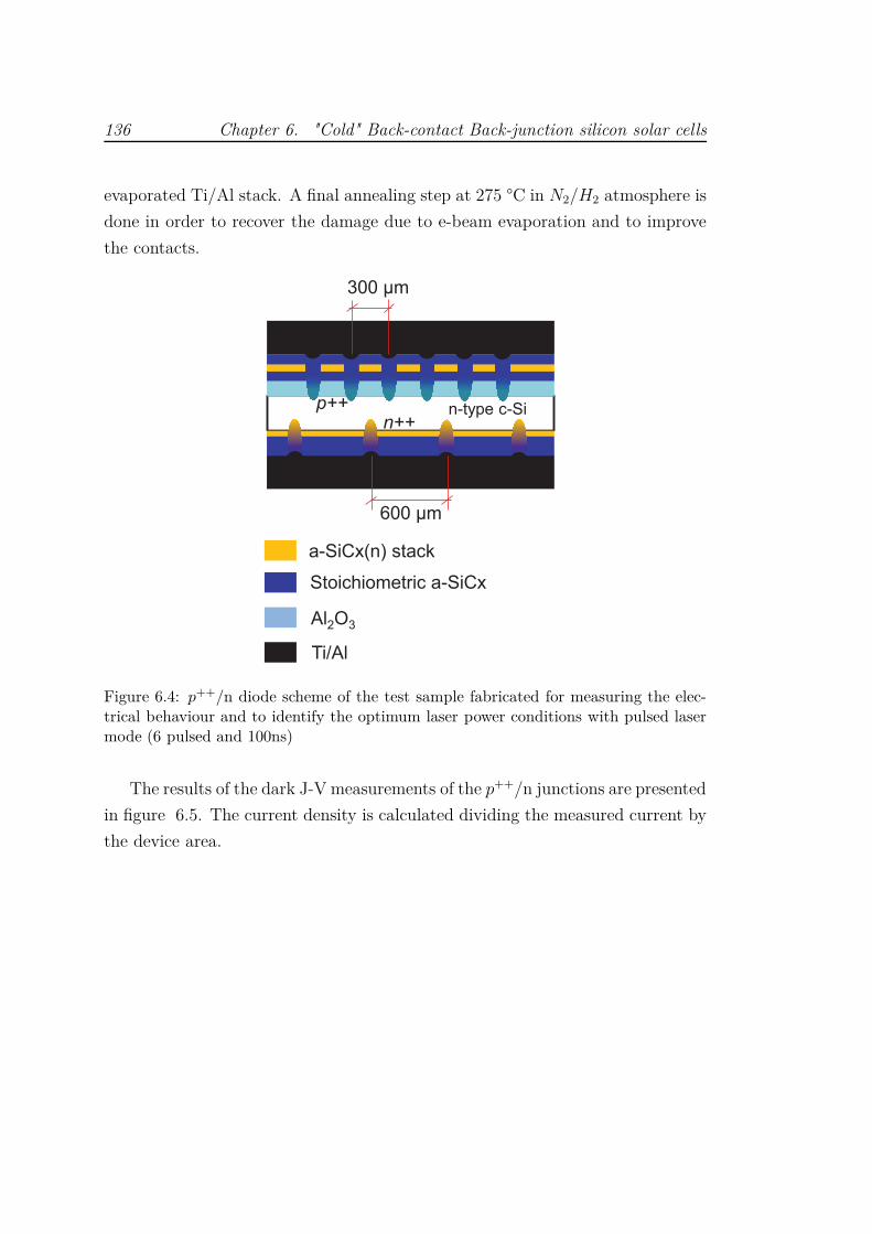
136 Chapter 6. "Cold" Back-contact Back-junction silicon solar cells
evaporated Ti/Al stack. A final annealing step at 275 °C in N2/H2 atmosphere is
done in order to recover the damage due to e-beam evaporation and to improve
the contacts.
p++ n-type c-Si n++
300 µm
600 µm
a-SiCx(n) stack
Stoichiometric a-SiCx
Al2O3
Ti/Al
Figure 6.4: p++/n diode scheme of the test sample fabricated for measuring the elec-trical behaviour and to identify the optimum laser power conditions with pulsed lasermode (6 pulsed and 100ns)
The results of the dark J-V measurements of the p++/n junctions are presented
in figure 6.5. The current density is calculated dividing the measured current by
the device area.
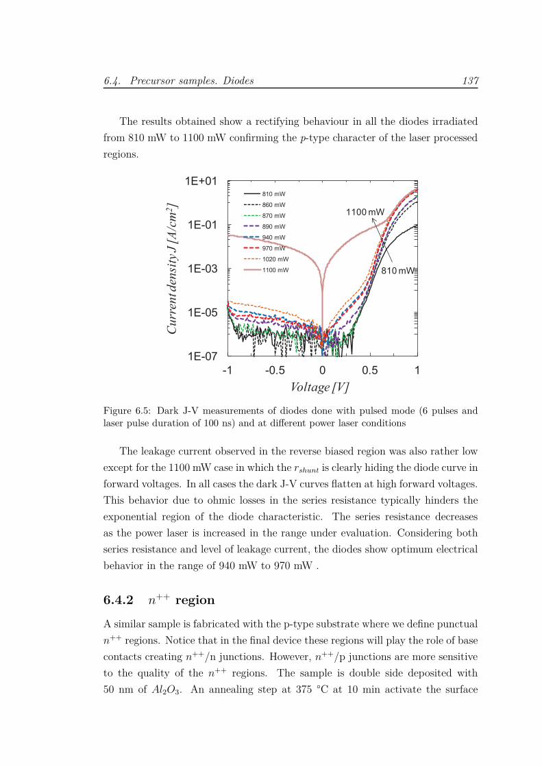
6.4. Precursor samples. Diodes 137
The results obtained show a rectifying behaviour in all the diodes irradiated
from 810 mW to 1100 mW confirming the p-type character of the laser processed
regions.
1E-07
1E-05
1E-03
1E-01
1E+01
-1 -0.5 0 0.5 1
Cu
rren
t den
sity
J [
A/c
m2]
Voltage [V]
810 mW
860 mW
870 mW
890 mW
940 mW
970 mW
1020 mW
1100 mW 810 mW
1100 mW
Figure 6.5: Dark J-V measurements of diodes done with pulsed mode (6 pulses andlaser pulse duration of 100 ns) and at different power laser conditions
The leakage current observed in the reverse biased region was also rather low
except for the 1100 mW case in which the rshunt is clearly hiding the diode curve in
forward voltages. In all cases the dark J-V curves flatten at high forward voltages.
This behavior due to ohmic losses in the series resistance typically hinders the
exponential region of the diode characteristic. The series resistance decreases
as the power laser is increased in the range under evaluation. Considering both
series resistance and level of leakage current, the diodes show optimum electrical
behavior in the range of 940 mW to 970 mW .
6.4.2 n++ region
A similar sample is fabricated with the p-type substrate where we define punctual
n++ regions. Notice that in the final device these regions will play the role of base
contacts creating n++/n junctions. However, n++/p junctions are more sensitive
to the quality of the n++ regions. The sample is double side deposited with
50 nm of Al2O3. An annealing step at 375 °C at 10 min activate the surface
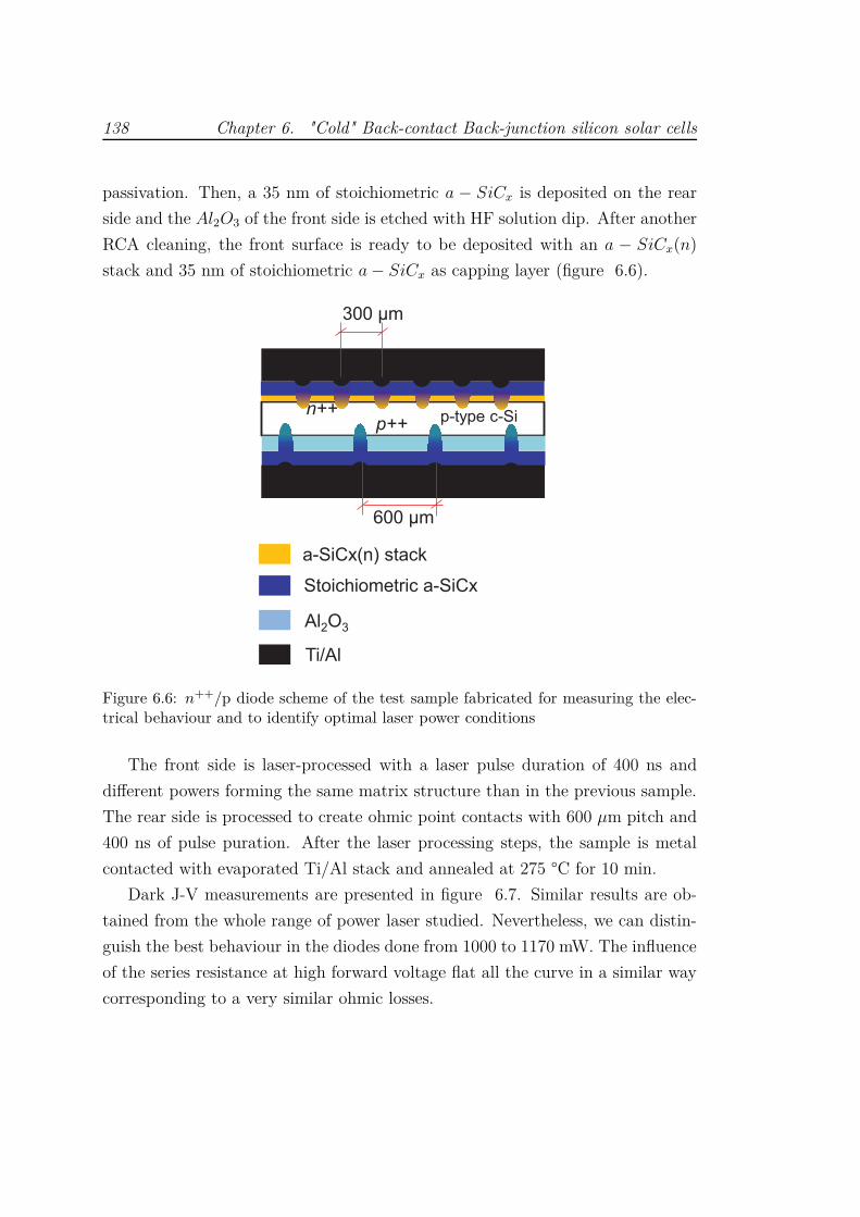
138 Chapter 6. "Cold" Back-contact Back-junction silicon solar cells
passivation. Then, a 35 nm of stoichiometric a − SiCx is deposited on the rear
side and the Al2O3 of the front side is etched with HF solution dip. After another
RCA cleaning, the front surface is ready to be deposited with an a − SiCx(n)
stack and 35 nm of stoichiometric a − SiCx as capping layer (figure 6.6).
300 µm
p-type c-Si p++
600 µm
a-SiCx(n) stack
Stoichiometric a-SiCx
Al2O3
Ti/Al
n++
Figure 6.6: n++/p diode scheme of the test sample fabricated for measuring the elec-trical behaviour and to identify optimal laser power conditions
The front side is laser-processed with a laser pulse duration of 400 ns and
different powers forming the same matrix structure than in the previous sample.
The rear side is processed to create ohmic point contacts with 600 µm pitch and
400 ns of pulse puration. After the laser processing steps, the sample is metal
contacted with evaporated Ti/Al stack and annealed at 275 °C for 10 min.
Dark J-V measurements are presented in figure 6.7. Similar results are ob-
tained from the whole range of power laser studied. Nevertheless, we can distin-
guish the best behaviour in the diodes done from 1000 to 1170 mW. The influence
of the series resistance at high forward voltage flat all the curve in a similar way
corresponding to a very similar ohmic losses.

6.5. Emitter saturation current (Joe) 139
1E-07
1E-06
1E-05
1E-04
1E-03
1E-02
1E-01
1E+00
1E+01
-1 -0.5 0 0.5 1
Cu
rren
t den
sity
J [
A/c
m2]
Voltage [V]
910 mW
1000 mW
1070 mW
1170 mW
1290 mW
Figure 6.7: Dark J-V measurements of n++/p diodes done with a fixed laser pulseduration of 400 ns and at different power laser conditions
6.5 Emitter saturation current (Joe)
Emitter saturation current density (Joe) is determined measuring effective lifetime
before and after the laser stage. The sample consists of a n-type c-Si in which
the front side is covered with 50 nm of Al2O3 + 35 nm stoichiometric a − SiCx
+ ∼ 20 nm a − Si(n) stack + 35 nm stoichiometric a − SiCx as in the final solar
cell. The rear side is passivated with 50 nm Al2O3. The test structure is shown
in figure 6.8. Then, we irradiate the front surface following a squared pattern
with a pitch of 600 µm. Laser conditions are the optimum ones determined in
the previous section: pulsed laser mode (6 pulses), pulse duration of 100 ns and
970 mW of laser power. The observed loss of the τeff after the laser stage can be
assumed caused by the recombination induced by the laser processed regions.
Joe is determined from the slope of the 1/τeff vs. ∆n (excess carrier density,
cm−3) at high injection using the "slope" method [1] (see Fig. 6.9). The slope of
the inverse lifetime is then proportional to Joe according to the equation:
1τeff,f
=1
τeff,o
+Joe
qn2i W
∆n (6.1)
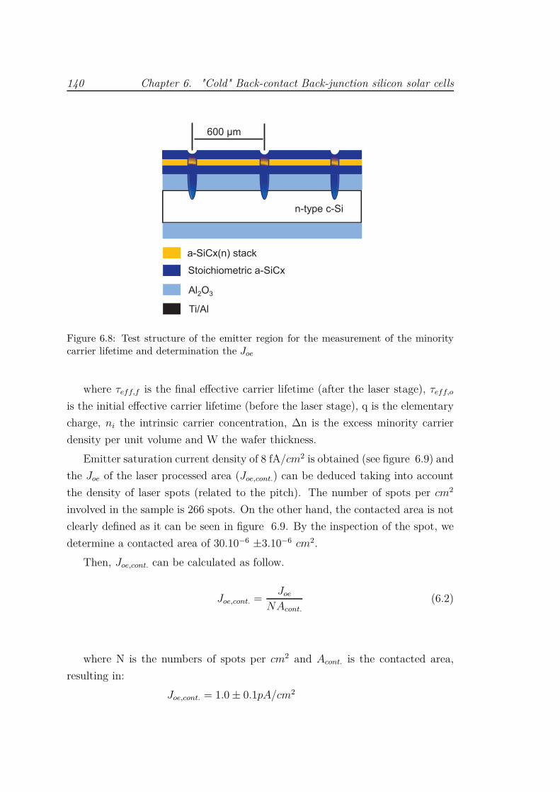
140 Chapter 6. "Cold" Back-contact Back-junction silicon solar cells
n-type c-Si
600 µm
a-SiCx(n) stack
Stoichiometric a-SiCx
Al2O3
Ti/Al
Figure 6.8: Test structure of the emitter region for the measurement of the minoritycarrier lifetime and determination the Joe
where τeff,f is the final effective carrier lifetime (after the laser stage), τeff,o
is the initial effective carrier lifetime (before the laser stage), q is the elementary
charge, ni the intrinsic carrier concentration, ∆n is the excess minority carrier
density per unit volume and W the wafer thickness.
Emitter saturation current density of 8 fA/cm2 is obtained (see figure 6.9) and
the Joe of the laser processed area (Joe,cont.) can be deduced taking into account
the density of laser spots (related to the pitch). The number of spots per cm2
involved in the sample is 266 spots. On the other hand, the contacted area is not
clearly defined as it can be seen in figure 6.9. By the inspection of the spot, we
determine a contacted area of 30.10−6 ±3.10−6 cm2.
Then, Joe,cont. can be calculated as follow.
Joe,cont. =Joe
NAcont.
(6.2)
where N is the numbers of spots per cm2 and Acont. is the contacted area,
resulting in:
Joe,cont. = 1.0 ± 0.1pA/cm2
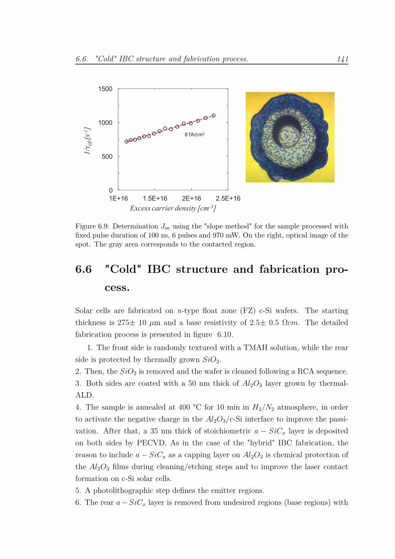
6.6. "Cold" IBC structure and fabrication process. 141
1/
eff[s
-1]
Excess carrier density [cm-3]
Figure 6.9: Determination Joe using the "slope method" for the sample processed withfixed pulse duration of 100 ns, 6 pulses and 970 mW. On the right, optical image of thespot. The gray area corresponds to the contacted region.
6.6 "Cold" IBC structure and fabrication pro-
cess.
Solar cells are fabricated on n-type float zone (FZ) c-Si wafers. The starting
thickness is 275± 10 µm and a base resistivity of 2.5± 0.5 Ωcm. The detailed
fabrication process is presented in figure 6.10.
1. The front side is randomly textured with a TMAH solution, while the rear
side is protected by thermally grown SiO2.
2. Then, the SiO2 is removed and the wafer is cleaned following a RCA sequence.
3. Both sides are coated with a 50 nm thick of Al2O3 layer grown by thermal-
ALD.
4. The sample is annealed at 400 °C for 10 min in H2/N2 atmosphere, in order
to activate the negative charge in the Al2O3/c-Si interface to improve the passi-
vation. After that, a 35 nm thick of stoichiometric a − SiCx layer is deposited
on both sides by PECVD. As in the case of the "hybrid" IBC fabrication, the
reason to include a − SiCx as a capping layer on Al2O3 is chemical protection of
the Al2O3 films during cleaning/etching steps and to improve the laser contact
formation on c-Si solar cells.
5. A photolithographic step defines the emitter regions.
6. The rear a − SiCx layer is removed from undesired regions (base regions) with
142 Chapter 6. "Cold" Back-contact Back-junction silicon solar cells
plasma etching (CF4).
7 and 8. The rear Al2O3 layer is wet etched from the base region with a HF
solution and the photoresist is stripped.
9. After a RCA cleaning, we deposit on the entire rear side the a−SiCx(n) stack
and 35 nm thick of stoichiometric a − SiCx.
10. BSF (n++) and emitter (p++) regions result from the laser irradiation of
these dielectric layers applying a pulsed Nd-YAG 1064 nm laser in the nanosec-
ond regime. Contacts are defined in a point-like structure with a pitch of 250 µm.
The laser conditions are 100 ns of pulse duration, 6 pulses per spot and 1100 mW
of laser power for the point-like emitter formation and 400 ns of pulse duration
and 1070 mW of laser power for the point-like BSF formation. The reason to ap-
ply 1100 mW instead of the optimum laser power for the emitter formation, i.e.
940-970 mW is because during the laser stage most of the spots were not formed
at this power and it was necessary to increase it in order to form all the punctual
emitters. That means that the energy delivered per unit of area (fluence) also
increases and consequently its effects on the crystal lattice.
Following the same structure that in the "Hybrid" IBC, four emitter coverage are
defined: one base laser spot per 2, 3, 4 or 6 emitter spots, corresponding to 66,
75, 80 and 85 % emitter coverage respectively (see figure 6.11).
11. A Ti/Al stack is deposited on the whole rear side.
12 and 13. The metal interdigitated pattern is defined by photolithographic step
and wet etching in H3P O4 solution. 14. Finally, the photoresit is stripped and
the wafer is annealed in a N2/H2 atmosphere at 275 °C for 10 minutes.
The illuminated area on the front side is defined using an extra aluminium
thermal evaporation on the front surface. This aluminium layer is properly patter-
ned and aligned face to face with the rear side (electrode side) to act as a shadow
mask defining light windows of 3 cm x 3 cm as in the same way than "Hybrid"
solar cells.

6.6. "Cold" IBC structure and fabrication process. 143
Step 1. Front surface texturation
n-type c-Si
Step 2. Rear SiO2 etching
n-type c-Si
Step 3. 50 nm Al2O3 both sides deposition
n-type c-Si
Step 4. 35 nm Stoichiometric a − SiCx both sides deposition
n-type c-Si

144 Chapter 6. "Cold" Back-contact Back-junction silicon solar cells
Step 5. Photolithograpic step. Emitter definition
n-type c-Si
Step 6. Plasma (CF4) Stoichiometric a − SiCx etching
n-type c-Si
Step 7. Al2O3 etching
n-type c-Si
Step 8. Photoresist stripping
n-type c-Si
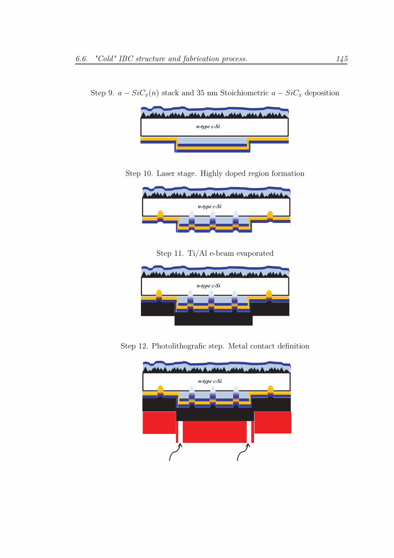
6.6. "Cold" IBC structure and fabrication process. 145
Step 9. a − SiCx(n) stack and 35 nm Stoichiometric a − SiCx deposition
n-type c-Si
Step 10. Laser stage. Highly doped region formation
n-type c-Si
Step 11. Ti/Al e-beam evaporated
n-type c-Si
Step 12. Photolithografic step. Metal contact definition
n-type c-Si
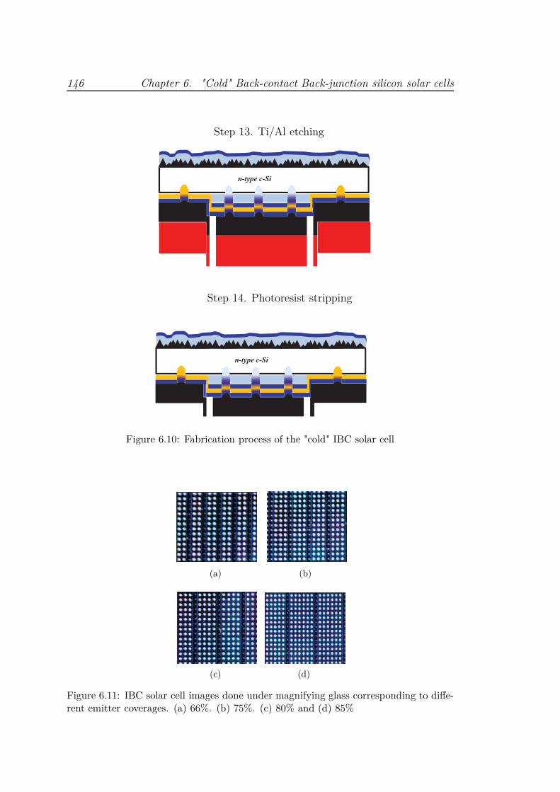
146 Chapter 6. "Cold" Back-contact Back-junction silicon solar cells
Step 13. Ti/Al etching
n-type c-Si
Step 14. Photoresist stripping
n-type c-Si
Figure 6.10: Fabrication process of the "cold" IBC solar cell
(a) (b)
(c) (d)
Figure 6.11: IBC solar cell images done under magnifying glass corresponding to diffe-rent emitter coverages. (a) 66%. (b) 75%. (c) 80% and (d) 85%
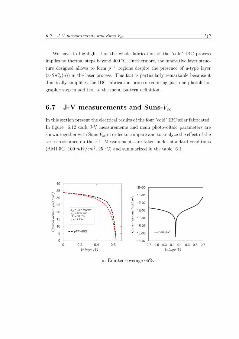
6.7. J-V measurements and Suns-Voc 147
We have to highlight that the whole fabrication of the "cold" IBC process
implies no thermal steps beyond 400 °C. Furthermore, the innovative layer struc-
ture designed allows to form p++ regions despite the presence of n-type layer
(a-SiCx(n)) in the laser process. This fact is particularly remarkable because it
drastically simplifies the IBC fabrication process requiring just one photolitho-
graphic step in addition to the metal pattern definition.
6.7 J-V measurements and Suns-Voc
In this section present the electrical results of the four "cold" IBC solar fabricated.
In figure 6.12 dark J-V measurements and main photovoltaic parameters are
shown together with Suns-Voc in order to compare and to analyze the effect of the
series resistance on the FF. Measurements are taken under standard conditions
(AM1.5G, 100 mW/cm2, 25 °C) and summarized in the table 6.1.
Cu
rren
t d
ensi
ty (
mA
/cm
2)
Voltage (V)
Cu
rren
t d
ensi
ty (
mA
/cm
2)
Voltage (V)
a. Emitter coverage 66%.
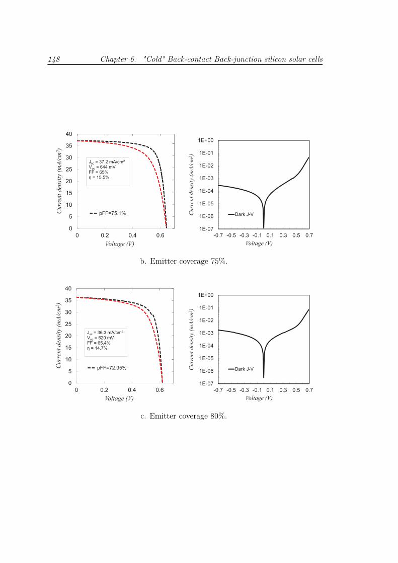
148 Chapter 6. "Cold" Back-contact Back-junction silicon solar cellsC
urr
ent
den
sity
(m
A/c
m2)
Voltage (V)
Cu
rren
t d
ensi
ty (
mA
/cm
2)
Voltage (V)
b. Emitter coverage 75%.
Cu
rren
t d
ensi
ty (
mA
/cm
2)
Voltage (V)
Cu
rren
t d
ensi
ty (
mA
/cm
2)
Voltage (V)
c. Emitter coverage 80%.
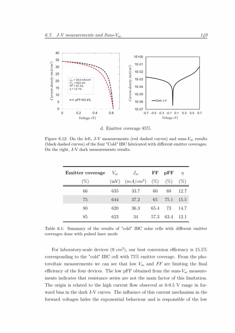
6.7. J-V measurements and Suns-Voc 149
Curr
ent
den
sity
(m
A/c
m2)
Voltage (V)
Cu
rren
t d
ensi
ty (
mA
/cm
2)
Voltage (V)
d. Emitter coverage 85%.
Figure 6.12: On the left, J-V measurements (red dashed curves) and suns-Voc results(black dashed curves) of the four "Cold" IBC fabricated with different emitter coverages.On the right, J-V dark measurements results.
Emitter coverage Voc Jsc FF pFF η
(%) (mV) (mA/cm2) (%) (%) (%)
66 635 33.7 60 68 12.7
75 644 37.2 65 75.1 15.5
80 620 36.3 65.4 73 14.7
85 623 34 57.3 63.4 12.1
Table 6.1: Summary of the results of "cold" IBC solar cells with different emittercoverages done with pulsed laser mode
For laboratory-scale devices (9 cm2), our best conversion efficiency is 15.5%
corresponding to the "cold" IBC cell with 75% emitter coverage. From the pho-
tovoltaic measurements we can see that low Voc and FF are limiting the final
efficiency of the four devices. The low pFF obtained from the suns-Voc measure-
ments indicates that resistance series are not the main factor of this limitation.
The origin is related to the high current flow observed at 0-0.5 V range in for-
ward bias in the dark J-V curves. The influence of this current mechanism in the
forward voltages hides the exponential behaviour and is responsible of the low
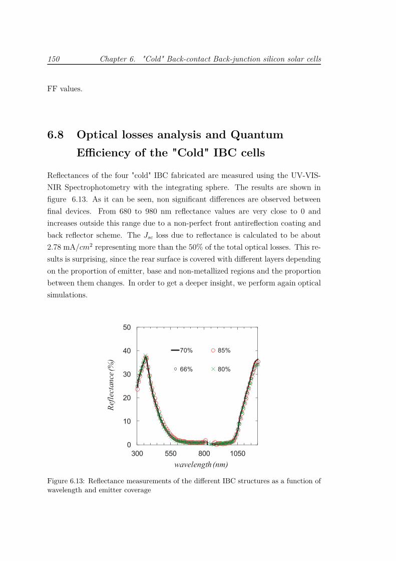
150 Chapter 6. "Cold" Back-contact Back-junction silicon solar cells
FF values.
6.8 Optical losses analysis and Quantum
Efficiency of the "Cold" IBC cells
Reflectances of the four "cold" IBC fabricated are measured using the UV-VIS-
NIR Spectrophotometry with the integrating sphere. The results are shown in
figure 6.13. As it can be seen, non significant differences are observed between
final devices. From 680 to 980 nm reflectance values are very close to 0 and
increases outside this range due to a non-perfect front antireflection coating and
back reflector scheme. The Jsc loss due to reflectance is calculated to be about
2.78 mA/cm2 representing more than the 50% of the total optical losses. This re-
sults is surprising, since the rear surface is covered with different layers depending
on the proportion of emitter, base and non-metallized regions and the proportion
between them changes. In order to get a deeper insight, we perform again optical
simulations.
0
10
20
30
40
50
300 550 800 1050
Ref
lect
an
ce (%
)
wavelength (nm)
70% 85%
66% 80%
Figure 6.13: Reflectance measurements of the different IBC structures as a function ofwavelength and emitter coverage
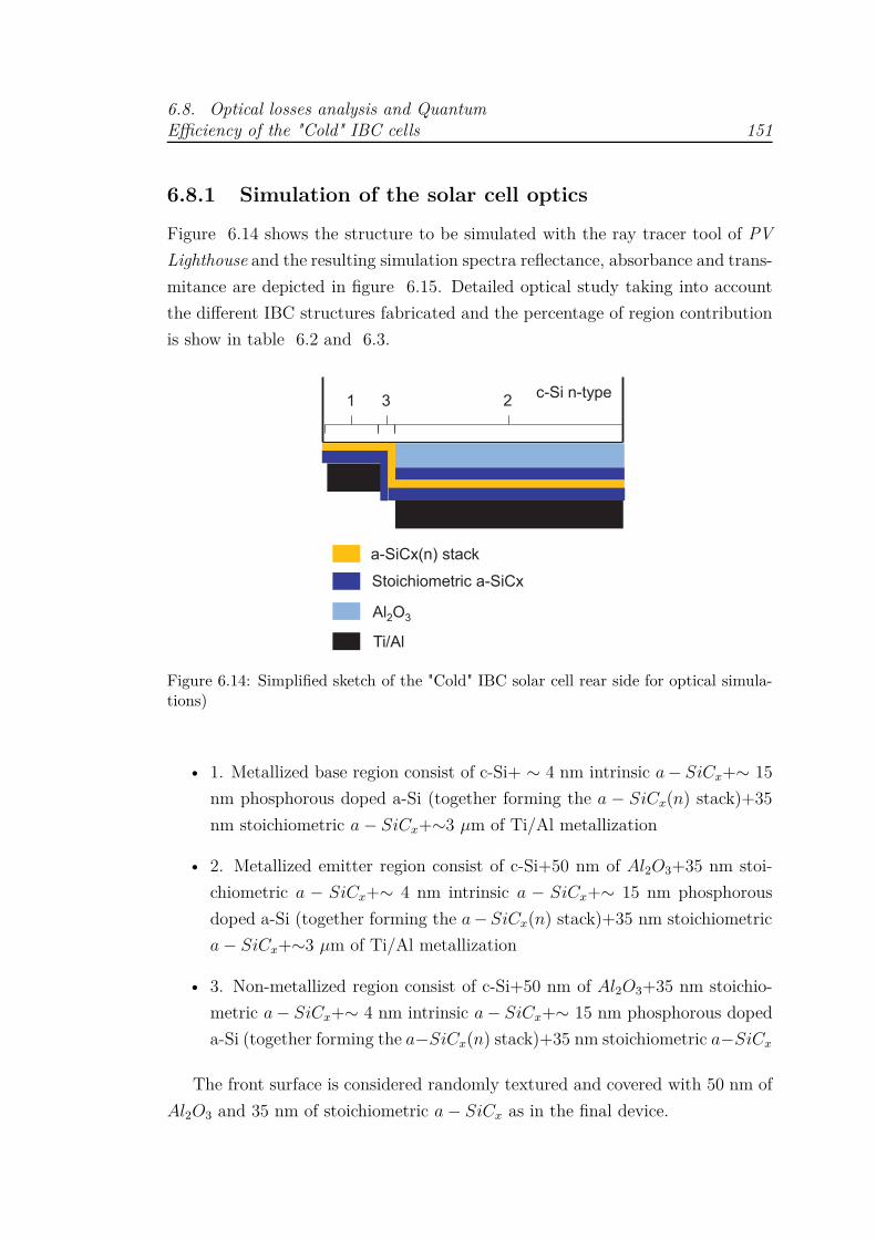
6.8. Optical losses analysis and QuantumEfficiency of the "Cold" IBC cells 151
6.8.1 Simulation of the solar cell optics
Figure 6.14 shows the structure to be simulated with the ray tracer tool of PV
Lighthouse and the resulting simulation spectra reflectance, absorbance and trans-
mitance are depicted in figure 6.15. Detailed optical study taking into account
the different IBC structures fabricated and the percentage of region contribution
is show in table 6.2 and 6.3.
c-Si n-type 1 2 3
a-SiCx(n) stack
Stoichiometric a-SiCx
Al2O3
Ti/Al
Figure 6.14: Simplified sketch of the "Cold" IBC solar cell rear side for optical simula-tions)
• 1. Metallized base region consist of c-Si+ ∼ 4 nm intrinsic a − SiCx+∼ 15
nm phosphorous doped a-Si (together forming the a − SiCx(n) stack)+35
nm stoichiometric a − SiCx+∼3 µm of Ti/Al metallization
• 2. Metallized emitter region consist of c-Si+50 nm of Al2O3+35 nm stoi-
chiometric a − SiCx+∼ 4 nm intrinsic a − SiCx+∼ 15 nm phosphorous
doped a-Si (together forming the a − SiCx(n) stack)+35 nm stoichiometric
a − SiCx+∼3 µm of Ti/Al metallization
• 3. Non-metallized region consist of c-Si+50 nm of Al2O3+35 nm stoichio-
metric a − SiCx+∼ 4 nm intrinsic a − SiCx+∼ 15 nm phosphorous doped
a-Si (together forming the a−SiCx(n) stack)+35 nm stoichiometric a−SiCx
The front surface is considered randomly textured and covered with 50 nm of
Al2O3 and 35 nm of stoichiometric a − SiCx as in the final device.
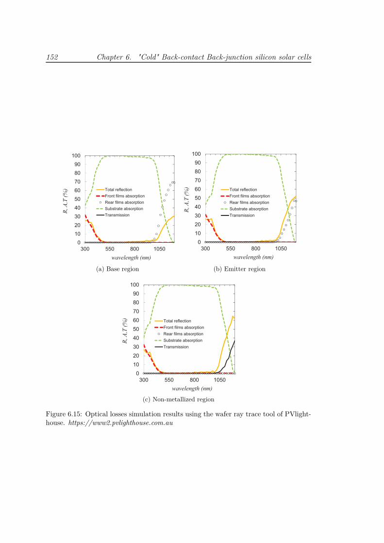
152 Chapter 6. "Cold" Back-contact Back-junction silicon solar cellsR
, A
,T (
%)
wavelength (nm)
Figura 7_base
(a) Base region
R, A
,T (
%)
wavelength (nm)
(b) Emitter region
R, A
,T (
%)
wavelength (nm)
(c) Non-metallized region
Figure 6.15: Optical losses simulation results using the wafer ray trace tool of PVlight-house. https://www2.pvlighthouse.com.au

6.8. Optical losses analysis and QuantumEfficiency of the "Cold" IBC cells 153
Optical losses [mA/cm2]
E. cover. Distrib. Reflec. Absorp. Trans.
[%] Emitter [%] Ext. Esc. Front Rear
Base[%]
Non-metal.[%]
50.1 0.50 1.04 0.20 0.86 -
66 29.5 0.30 0.34 0.12 1.04 -
20.4 0.20 0.49 0.08 3.16.10−16 0.21
63.7 0.63 1.32 0.26 1.1 -
75 23.7 0.24 0.27 0.09 0.83 -
12.6 0.12 0.30 0.05 1.9.10−16 0.13
68 0.67 1.41 0.28 1.17 -
80 20 0.20 0.23 0.08 0.70 -
12 0.12 0.29 0.05 1.8.10−16 0.12
79.6 0.79 1.65 0.32 1.37 -
85 16.8 0.17 0.19 0.07 0.59 -
3.6 0.03 0.08 0.01 5.58.10−17 0.04
Table 6.2: Optical losses distribution depending on rear IBC region and emitter cove-rage
IBC Reflect. Absorp. Transmit. Total loss Ph. (Absorbed)
% coverage [mA/cm2] [mA/cm2] [mA/cm2] [mA/cm2] [mA/cm2]
66 2.87 2.30 0.21 5.38. 41.28
75 2.88 2.33 0.13 5.34 41.30
80 2.92 2.28 0.12 5.32 41.33
85 2.91 2.36 0.04 5.31 41.33
Table 6.3: Optical losses distribution depending of rear IBC region and emitter coverage

154 Chapter 6. "Cold" Back-contact Back-junction silicon solar cells
The largest loss mechanism is the escape surface reflectance together with the
transmission losses in the non-metallized zone. The escape surface reflectance
is caused by non-ideal light-trapping and is also considerable in the base and
emitter region together with parasitic absorption of the rear films, mainly due to
the titanium film. The external reflectance is related to non-optimal properties of
the antireflection coating (Al2O3 and stoichiometric a−SiCx) that is common for
the three zones. The parasitic front film absorption losses is due to the absorption
of the stoichiometric a−SiCx below 450 nm. Al2O3 does not absorbs in the whole
evaluated range.
Table 6.2 and 6.3 show a detailed analysis of the optical losses as a function
of the emitter coverage. The study reveals that the Jsc current density loss due
to the optical losses is very similar between the different IBC structures (∼ 5.3
mA/cm2) most of them related to the emitter regions. As we can see from the
simulated results (table 6.3), the total reflection losses are between 2.8 and 2.9
mA/cm2 that agrees with the value obtained from the experimental measurement.
In general, we can say that different regions contribute with similar values to the
optical losses resulting in a weak dependence on the emitter coverage.
6.8.2 External quantum efficiency analysis
In figure 6.16a the measured external quantum efficiency (EQE) of the "cold" IBC
cells are depicted. The EQE responses are strongly impacted by the front surface
recombination velocity and the non-ideal front surface passivation is responsible
of the major photocurrent (Jph) loss mechanism. Best results are achieved for
the "cold" IBCs with 75 and 80% emitter coverage, probably due to a better
front surface passivation. Additionally, IQE and reflectance of the best "cold"
IBC fabricated (75% emitter coverage) is calculated from experimental data as
IQE = EQE/(1 − R) and represented in figure 6.16b. The drop observed below
the 500 nm wavelength is due to the parasitic absorption of the 35 nm thick of
stoichiometric a-SiCx in the front of the cell as it was concluded in the study
carried out in the chapter 3.
In order to compare the impact of Sfront in the IQE response, we have simu-
lated IQE curves assuming different front surface recombination velocities as in
the same way than in the "Hybrid" solar cells. The approximation to the Sfront
value is obtained by fitting the experimental IQE curve (black circles symbols,
figure 6.17) with the simulated IQEs curve calculated with PC-1D (red dashed

6.8. Optical losses analysis and QuantumEfficiency of the "Cold" IBC cells 155
0
10
20
30
40
50
60
70
80
90
100
300 550 800 1050
EQ
E (%
)
wavelength (nm)
66%
75%
80%
85%
(a)
0
10
20
30
40
50
60
70
80
90
100
300 550 800 1050
Ref
lect
an
ce (%
)
IQE
(%
)
wavelength (nm)
IQE Calculed
EQE
Reflectance
(b)
Figure 6.16: (a) EQEs measurements of the four different "Cold" IBC structures (b)EQE, IQE and Reflectance measurements of the "Cold" IBC with 75% emitter coverage
lines, in the same figure). The simulated IBC device is simplified by means of a
simple back junction structure with the same device features (thickness, substrate
doping density and experimental reflectance). Simulations are done for different
Sfront values, 20, 40 and 60 cm/s, resulting 40 cm/s the best choice for the fitting.
From the comparative between experimental and simulated IQE curves it can be
seen that, as in the case of "Hybrid" IBC, front surface passivation is good enough
(Sfront=40 cm/s) to assume that the low Voc obtained is again probably due to a
high recombination at the rear side.
The laser-induced crystal damage is partially responsible of the low Voc values.
The pulse energy had to be increased above the optimal power to form all the
punctual emitters. The high energy can ablate the surface introducing damage
to the silicon lattice. These defects are recombination centers that affect the
lifetime of the minority carriers resulting in low Voc [2]. Another cause of these
low Voc values could be the poor rear surface passivation either in base regions
and emitter region. During the fabrication process, specially after the CF4 dry
etching (step 6 of the fabrication process) the surface passivation substantially
worsens and it is just partially recovered after an annealing step.
It is clear that the loss in the surface passivation quality (due to the plasma
etching with CF4 at the rear side) and the damage introduced by the laser are the
two main factors to be improved for better Voc and FF values and consequently
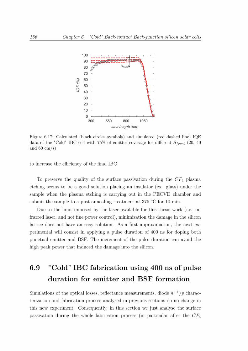
156 Chapter 6. "Cold" Back-contact Back-junction silicon solar cells
0
10
20
30
40
50
60
70
80
90
100
300 550 800 1050
IQE
(%
)
wavelength (nm)
Sfront
Figure 6.17: Calculated (black circles symbols) and simulated (red dashed line) IQEdata of the "Cold" IBC cell with 75% of emitter coverage for different Sfront (20, 40and 60 cm/s)
to increase the efficiency of the final IBC.
To preserve the quality of the surface passivation during the CF4 plasma
etching seems to be a good solution placing an insulator (ex. glass) under the
sample when the plasma etching is carrying out in the PECVD chamber and
submit the sample to a post-annealing treatment at 375 °C for 10 min.
Due to the limit imposed by the laser available for this thesis work (i.e. in-
frarred laser, and not fine power control), minimization the damage in the silicon
lattice does not have an easy solution. As a first approximation, the next ex-
perimental will consist in applying a pulse duration of 400 ns for doping both
punctual emitter and BSF. The increment of the pulse duration can avoid the
high peak power that induced the damage into the silicon.
6.9 "Cold" IBC fabrication using 400 ns of pulse
duration for emitter and BSF formation
Simulations of the optical losses, reflectance measurements, diode n++/p charac-
terization and fabrication process analysed in previous sections do no change in
this new experiment. Consequently, in this section we just analyse the surface
passivation during the whole fabrication process (in particular after the CF4

6.9. "Cold" IBC fabrication using 400 ns of pulse duration for emitter and BSFformation 157
plasma etching and post-annealing step) and the p++/n diodes done with a pulse
duration of 400 ns at different laser powers. Finally, we fabricate and characterize
the "Cold" IBCs using the new optimized laser parameters.
6.9.1 "Cold" IBC surface passivation
The Seff,max is affected in every fabrication step. In figure 6.18 we show the
Seff,max values calculated after each fabrication step. We can observe that Seff,max
strongly increases after CF4 plasma etching. Then, after the annealing step at
400 °C for 10 min, the passivation quality is recovered.
Sef
f,m
ax(
cm/s
)
Fabrication steps
Figure 6.18: Seff,max value at one-sun illumination during the "cold" IBC solar cellfabrication
6.9.2 Precursor samples. Diodes p++/n
Diodes precursor done for this experimental follow the same structure and fab-
rication process than in previous section (6.3.1). The only difference is the laser
processing. In this experimental the front side of the precursor diodes are done
with a laser pulse duration of 400 ns and at different laser powers.
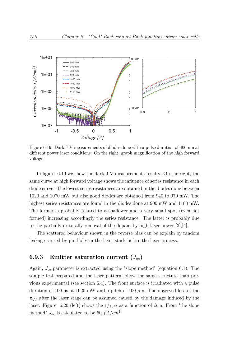
158 Chapter 6. "Cold" Back-contact Back-junction silicon solar cells
1E-07
1E-05
1E-03
1E-01
1E+01
-1 -0.5 0 0.5 1
Cu
rren
t den
sity
J [
A/c
m2]
Voltage [V]
900 mW
940 mW
960 mW
970 mW
1020 mW
1040 mW
1070 mW
1110 mW
1E-01
1E+01
0.8 0.9 1
Figure 6.19: Dark J-V measurements of diodes done with a pulse duration of 400 nm atdifferent power laser conditions. On the right, graph magnification of the high forwardvoltage
In figure 6.19 we show the dark J-V measurements results. On the right, the
same curve at high forward voltage shows the influence of series resistance in each
diode curve. The lowest series resistances are obtained in the diodes done between
1020 and 1070 mW but also good diodes are obtained from 940 to 970 mW. The
highest series resistances are found in the diodes done at 900 mW and 1100 mW.
The former is probably related to a shallower and a very small spot (even not
formed) increasing accordingly the series resistance. The latter is probably due
to the partially or totally removal of the dopant by high laser power [3],[4].
The scattered behaviour shown in the reverse bias can be explain by random
leakage caused by pin-holes in the layer stack before the laser process.
6.9.3 Emitter saturation current (Joe)
Again, Joe parameter is extracted using the "slope method" (equation 6.1). The
sample test prepared and the laser pattern follow the same structure than pre-
vious experimental (see section 6.4). The front surface is irradiated with a pulse
duration of 400 ns at 1020 mW and a pitch of 400 µm. The observed loss of the
τeff after the laser stage can be assumed caused by the damage induced by the
laser. Figure 6.20 (left) shows the 1/τeff as a function of ∆ n. From "the slope
method" Joe is calculated to be 60 fA/cm2
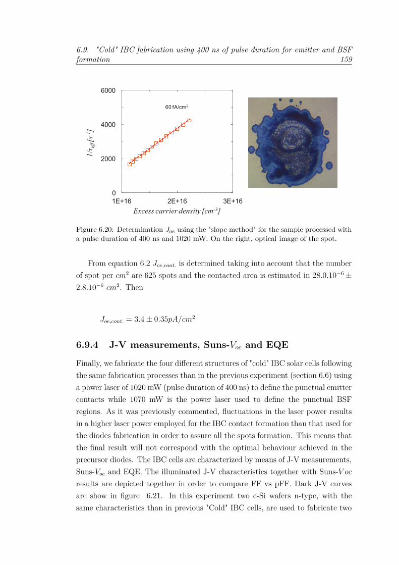
6.9. "Cold" IBC fabrication using 400 ns of pulse duration for emitter and BSFformation 159
0
2000
4000
6000
1E+16 2E+16 3E+16
1/
eff[s
-1]
Excess carrier density [cm-3]
60 fA/cm2
Figure 6.20: Determination Joe using the "slope method" for the sample processed witha pulse duration of 400 ns and 1020 mW. On the right, optical image of the spot.
From equation 6.2 Joe,cont. is determined taking into account that the number
of spot per cm2 are 625 spots and the contacted area is estimated in 28.0.10−6 ±
2.8.10−6 cm2. Then
Joe,cont. = 3.4 ± 0.35pA/cm2
6.9.4 J-V measurements, Suns-Voc and EQE
Finally, we fabricate the four different structures of "cold" IBC solar cells following
the same fabrication processes than in the previous experiment (section 6.6) using
a power laser of 1020 mW (pulse duration of 400 ns) to define the punctual emitter
contacts while 1070 mW is the power laser used to define the punctual BSF
regions. As it was previously commented, fluctuations in the laser power results
in a higher laser power employed for the IBC contact formation than that used for
the diodes fabrication in order to assure all the spots formation. This means that
the final result will not correspond with the optimal behaviour achieved in the
precursor diodes. The IBC cells are characterized by means of J-V measurements,
Suns-Voc and EQE. The illuminated J-V characteristics together with Suns-V oc
results are depicted together in order to compare FF vs pFF. Dark J-V curves
are show in figure 6.21. In this experiment two c-Si wafers n-type, with the
same characteristics than in previous "Cold" IBC cells, are used to fabricate two
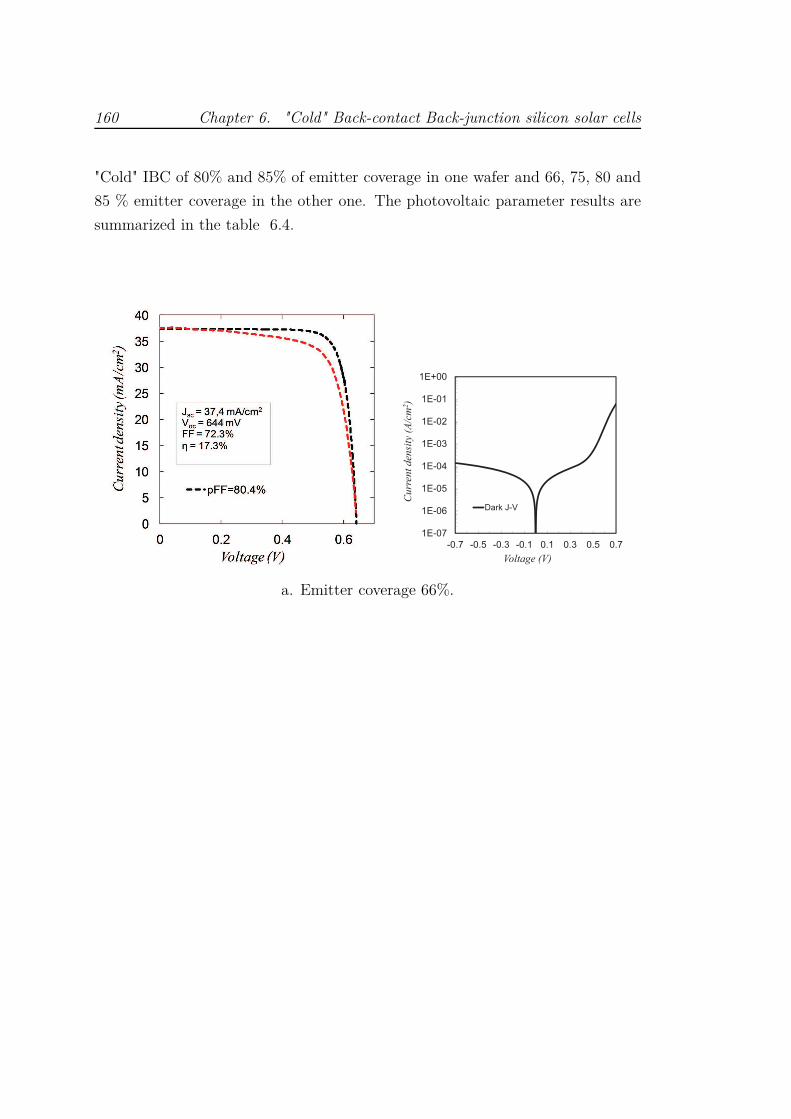
160 Chapter 6. "Cold" Back-contact Back-junction silicon solar cells
"Cold" IBC of 80% and 85% of emitter coverage in one wafer and 66, 75, 80 and
85 % emitter coverage in the other one. The photovoltaic parameter results are
summarized in the table 6.4.
Cu
rren
t d
ensi
ty (
A/c
m2)
Voltage (V)
a. Emitter coverage 66%.
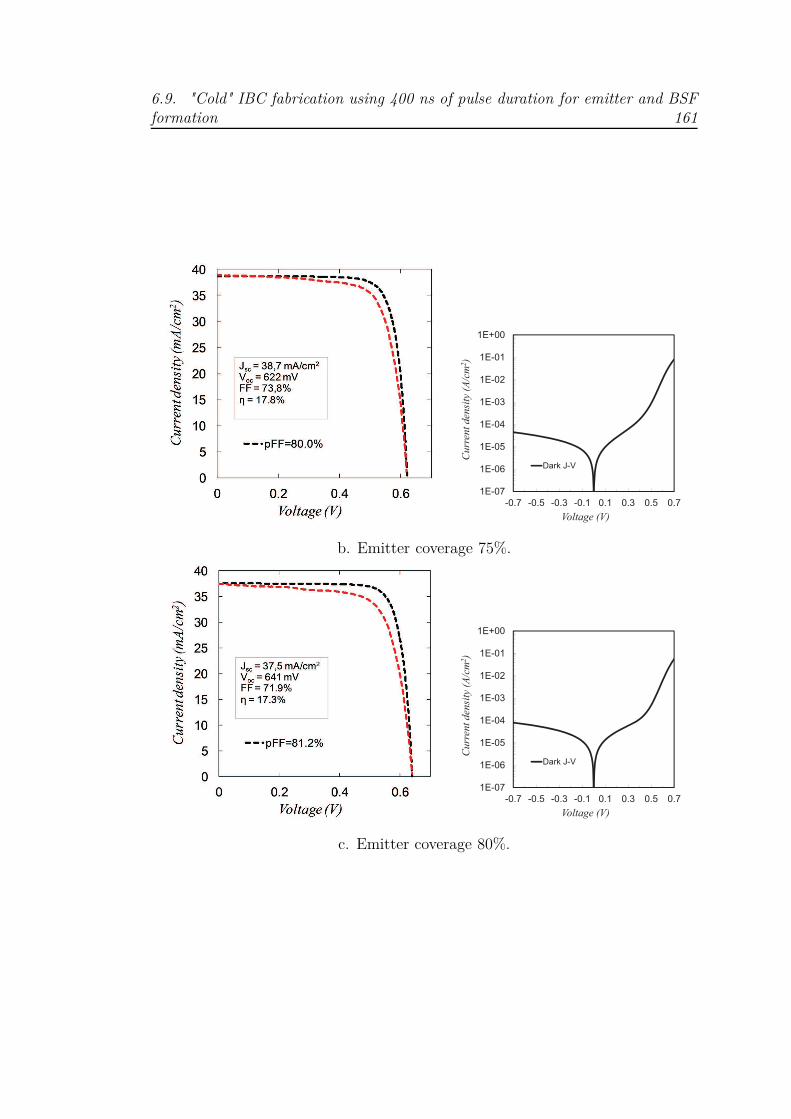
6.9. "Cold" IBC fabrication using 400 ns of pulse duration for emitter and BSFformation 161
Cu
rren
t d
ensi
ty (
A/c
m2)
Voltage (V)
b. Emitter coverage 75%.
Cu
rren
t d
ensi
ty (
A/c
m2)
Voltage (V)
c. Emitter coverage 80%.

162 Chapter 6. "Cold" Back-contact Back-junction silicon solar cells
Cu
rren
t d
ensi
ty (
A/c
m2)
Voltage (V)
d. Emitter coverage 85%.
Figure 6.21: Wafer 1. On the left, J-V measurements of different emitter coverage of"Cold" IBC solar cells (red dashed lines) and suns-Voc results (black dashed lines). Onthe right, J-V Dark measurements results.
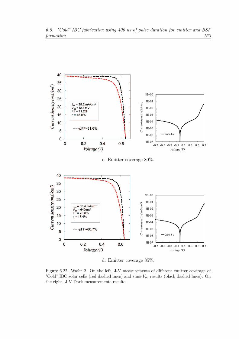
6.9. "Cold" IBC fabrication using 400 ns of pulse duration for emitter and BSFformation 163
1E-07
1E-06
1E-05
1E-04
1E-03
1E-02
1E-01
1E+00
-0.7 -0.5 -0.3 -0.1 0.1 0.3 0.5 0.7
Cu
rren
t den
sity
(A
/cm
2)
Voltage (V)
Dark J-V
c. Emitter coverage 80%.
1E-07
1E-06
1E-05
1E-04
1E-03
1E-02
1E-01
1E+00
-0.7 -0.5 -0.3 -0.1 0.1 0.3 0.5 0.7
Cu
rren
t den
sity
(m
A/c
m2)
Voltage (V)
Dark J-V
d. Emitter coverage 85%.
Figure 6.22: Wafer 2. On the left, J-V measurements of different emitter coverage of"Cold" IBC solar cells (red dashed lines) and suns-Voc results (black dashed lines). Onthe right, J-V Dark measurements results.

164 Chapter 6. "Cold" Back-contact Back-junction silicon solar cells
Wafer Emitter coverage. Voc Jsc FF pFF η
(%) (mV) (mA/cm2) (%) (%) (%)
1
66 644 37.4 72.3 80.4 17.3
75 622 38.7 73.8 80.0 17.8
80 641 37.5 71.9 81.2 17.3
85 640 38.7 71.5 82.6 17.7
280 647 39.2 71.2 81.6 18.0
85 640 38.4 70.8 80.7 17.4
Table 6.4: Summary of the results of "cold" IBC solar cells with different emittercoverages done with 400 ns of pulse duration
As it can be seen in the above table, there is a general increment of the effi-
ciency in all the IBC cell obtaining the 18.0% in our best device. The increment
of the Jsc values agree with the improvement of the EQE responses (see figure
6.23a) .
0
10
20
30
40
50
60
70
80
90
100
300 550 800 1050
EQ
E (%
)
wavelength (nm)
66%
75%
80%, wafer 1
85%, wafer 1
80%, wafer 2
85%, wafer 2
(a)
0
10
20
30
40
50
60
70
80
90
100
300 550 800 1050
Ref
lect
an
ce (%
)
EQ
E,I
QE
(%
)
wavelength (nm)
(b)
Figure 6.23: a) EQEs measurements of the "Cold" IBC cell with different emittercoverages. b) EQE (black dashed), calculated IQE (black circles), simulated IQE (reddashed) and Reflectance (green dashed) measurements of the "Cold" IBC with 80%emitter coverage
The surface passivation achieved in the wafer 2 was better than in the wafer
6.9. "Cold" IBC fabrication using 400 ns of pulse duration for emitter and BSFformation 165
1. This improvement is clearly translated to a better EQE results (in all the
wavelength range) for the same emitter coverage cells. A remarkable 97% is
achieved from 620 nm to 960 nm. The difference in the EQE responses of the
different cells can be attributed to differences in the quality of the surface pa-
ssivation among them. The better surface passivation results in a decrease of
the surface recombination velocity helping photogenerated carriers to get to the
collecting contact. Again, the reduction in the EQE curve below 560 nm is due
to the front cell reflectance. The optical losses do not play a especial role in the
general improvement since the "Cold" IBCs developed with a pulse laser duration
of 400 ns follow exactly the same cell structure than those "Cold" IBCs with a
laser pulse duration of 100 ns and the latter cells have not achieved so high Jsc
values. Furthermore, we can also observe a remarkable increase of the Voc values
evidencing a clear improvement of surface passivation. In the figure 6.23b we
show the EQE, IQE and reflectance of the best "Cold" IBC obtained,i.e. 80%
of emitter coverage and the drop in the IQE below 450 nm indicate a parasitic
absorption of the front c-SiCx layer.
From the IQE fitting (figure 6.23b) we deduce a very low Sfront of 12 cm/s
and therefore the relative still low Voc values are affected by the rear surface
passivation. On the other hand, the damage in the passivation quality after the
laser processing (see section 6.10) point to the spot laser depassivation due to
the dielectric ablation. Additionally, we can say that the increase of the pulse
duration to a 400 ns decreases the laser-induced defects into the silicon structure
(a laser with longer pulsed allow to the silicon to recrystallize in a proper manner
avoiding the defect formation [5]). Consequently, and as it can be seen in the
reverse voltage in the dark J-V measurements the leakage current is considerably
reduced since the number of shunting path between the metal and the bulk is
decreased.
However, there is still some efficiency limitation mainly due to the low FF. The
high value of the pFF indicates that the main loss in the FF is due the Rs. Apart
from the IBC with emitter coverage of 75%, the results indicate that as the emitter
coverage increases the Rs reducing the pFF. The origin of this Rs can be in the
bulk resistance since the base contacts are more and more separated. As the
emitter coverage increases, the mean transport path of the electrons to the base
also increases and hence the resistance series. Another important contribution to

166 Chapter 6. "Cold" Back-contact Back-junction silicon solar cells
this series resistance can be related with a very resistive p- channel surrounding
p++ emitter contacts induced by the negative charge in the Si/Al2O3 interface.
6.10 Conclusion
In this chapter, we have developed our first "cold" IBC solar cells with different
emitter coverages on n-type c-Si substrates. We have eliminated any conventional
diffusion and simplified the fabrication process by removing photolithografic steps.
The dielectric layers employed as dopant source are the same than those used in
the "Hybrid" IBC, i.e. Al2O3 to dope the emitter regions (p++) and a-SiCx(n)
stack the BSF regions (n++). Additional stoichiometric a-SiCx was used for
chemical protection and to reduce the lattice damage induced during the laser
step. Optical losses have been also analyzed in order to know the main way
of photocurrent loss. We have demonstrated that the surface passivation and
the laser conditions are crucial to achieve high efficiency. The increment of the
pulse duration from 100 to 400 ns has reduced the laser-induced defects. In a
first approximation, the punctual emitters were created with a pulsed mode of 6
pulses (100 ns) while the BSF with a pulse duration of 400 ns achieving an effi-
ciency of 15.5% in our best cell. The final "Cold" IBC solar cells were fabricated
using a pulse duration of 400 ns to create both punctual emitter and BSF regions
achieving an impressive 18.0% of efficiency.
Finally we must point out that the instability of the laser system causes
missing pulse effect. Moreover, the difficult to achieve a good laser power control
for an infrared laser, leads to a very narrow processing windows and the small
increased in the beam energy, in order to avoid missing pulses, causes additional
crystal damage. Thus, the simplest way to prevent this damage is to avoid melting
an excessive volume of silicon, by controlling the laser power, difficult to achieve
in the infrared laser. The change to shorter laser wavelengths would lead to
shallower photon absorption and better power control. Consequently, less silicon
would be melted with less lattice damage.
Bibliography 167
Bibliography
[1] D.E Kane and R.M Swanson. Measurement of the emitter saturation current
by a contactless photoconductivity decay method. In 18th Photovoltaic Spe-
cialists Conference. IEEE, pages 578–583. IEEE, 1985.
[2] M. Abbott, P. Cousins, F. Chen, and J. Cotter. Laser-induced defects in
crystalline silicon solar cells. In 31st IEEE Photovoltaic Specialists Conference
(PVSC), Orlando, pages 1241–1244. IEEE, 2005.
[3] A. Fell, E. Franklin, D. Walter, D. Suh, and K. Weber. Laser Doping from
Al2O3 layers. In 27th European Photovoltaic Solar Energy Conference and
Exhibition, (Frankfurt), Germany, pages 706–708, 2012.
[4] Z. Hameiri, L. Mai, T. Puzzer, and S.R. Wenham. Influence of laser power
on the properties of laser doped solar cells. Solar Energy Materials and Solar
Cells, 95:1085–1094, 2011.
[5] B. Santoso. Laser doped selective emitter solar cells. PhD thesis, 2010.


Chapter 7
One step forward!. Achieving
high-efficiency solar cell
In this final chapter, we have developed the "Cold" IBC solar cells
following the same fabrication process used in the previous chapter,
but just changing the laser stage method. The main goal in this ex-
periment is to increase the solar cell efficiencies avoiding the lattice
damage induced by the infrared laser. We have optimized the laser-
doped contacts employing UV laser (355 nm) through the dielectric
stacks to create the highly-doped regions (p++ and n++) in one single
laser step. The laser power is controlled by means of an external atte-
nuator in the 20-200 mW range as a free parameter to be optimized.
Additionally, sheet resistance (Rsheet) and precursor diodes (p++/n
and n++/p) are analyzed in the same way that previous chapters to
optimize the laser conditions. The final devices are characterized by
EQE, Suns-Voc, and J-V measurements. Short-circuit densities and
open-circuit voltages about 40 mA/cm2 and 650 mV respectively and
efficiencies up to 20% have been obtained using this simplified baseline
process.
169
170 Chapter 7. One step forward!. Achieving high-efficiency solar cell
7.1 Optimization of laser-doped contacts
7.1.1 Laser system
The laser employed is located in Centro Laser, UPM (Universidad Politécnica
de Madrid) facilities. The laser is a diode-pumped, ns-pulsed, Nd:YVO4 system
(Spectra-Physics Hippo H10-355QW) operating at wavelength of 355 nm (UV).
and emitting with a TM0 gaussian mode beam with radius at focus of 15 µm.
Pulse duration and frequency are 12 ns and 20 kHz respectively. The laser power
is controlled by means of an external attenuator in the 20-200 mW and adjusted
just before each experiment thanks a thermocouple sensor. The laser beam can
be swept thanks to a galvo scanner (ScanLAB HurryScan II) up to 125 mm x 125
mm area and is focused using a z-theta lens (250 nm focal length). Samples were
mounted in a four axis manual stage, allowing 25 mm travel in the XY horizontal
directions, 12.5 mm travel in the Z vertical direction, and 360° rotation around Z
axis. Both the optical scanner and the manual stages have a position and angle
accuracy of ±10 µm and 0.01° respectively.
7.1.2 Sheet resistance (Rsheet) and precursor diodes
In order to optimize UV laser system for IBC manufacturing some test samples are
fabricated using n- and p-type high quality float zone FZ <100> c-Si 4 inch wafers
(2.5 ± 0.5 Ωcm, 275 ± 10 µm thick). The p++ doped regions are formed into
n-type c-Si processing the laser through Al2O3/stoichiometric a-SiCx/a-SiCx(n)
stack 1/stoichiometric a-SiCx stack layers (figure 7.2a) while the n++ doped
regions are processed into p-type c-Si through
a-SiCx(n)/stoichiometric a-SiCx (figure 7.2b).
Laser power tuning
Spot diameter as a function of laser power considering the two different stacks
involved in the IBC solar cell fabrication is shown in figure 7.1. Laser crater
morphology exhibits a circular-like shape with two different regions. On the
one hand an inner circular region with an internal diameter Din where dielectric
stack is fully removed and the silicon is clearly melt. On the other hand one ring
1a − SiCx(n) stack consists of ∼ 4 nm of silicon rich a − SiCx(i) and ∼ 15 nm phosphorousdoped a-Si

7.1. Optimization of laser-doped contacts 171
region with an inner and outer diameter Din and Dout respectively, where material
is partially ablated and surface/bulk recombination is significantly affected [1].
Nevertheless, from an electrical contact point of view, we consider that only the
inner circle is contacted in the subsequent metallization stage and its area allows
define the contact fraction area fc.
p++
n++
Figure 7.1: Spot diameter vs. laser power P. The above figure corresponds to p-typedoping and below to the n-type doping. Laser spot images corresponding to P ∼ 125mW are also shown in the insets.
As it is expected from results shown in 7.1, higher laser powers result in higher
Din and Dout values. Inner spot diameters are in the 5-17 and 14-35 µm range for
the stacks with and without Al2O3 layer respectively. It is important to remark
that p-type doping needs higher powers to form the contacts (> ∼90 mW) than
n-type doping counterparts (> ∼20 mW). In all cases, crater depths in the melted

172 Chapter 7. One step forward!. Achieving high-efficiency solar cell
region are well below 800 nm in the whole laser power range, indicating that UV
irradiation superficially affects silicon material minimizing potential deep bulk
damage after laser stage.
Sheet resistance
Samples are fabricated to explore the sheet resistances Rsh on large laser-doped
areas of 1 cm x 1 cm using the UV laser. Only the front side of the samples are
processed with the corresponding stacks (see figure 7.2). The contact pitch is
also adjusted to overlap laser spots to form continuous doped regions in order to
measure the Rsh using the four-point probe technique
n-type c-Si
1 cm
(a)
p-type c-Si
1 cm
(b)
a-SiCx(n) stack
Stoichiometric a-SiCx
Al2O3
Figure 7.2: Sample structures for sheet resistance test. a) p-type doping b) n--typedoping
Rsh measurements allow to determine a coarse laser power range to perform
the laser doping stage as it is shown in figure 7.3. It is clear that formation of
n++ emitters involves a broad window of useful powers in the 40-200 mW range,
however powers higher than ∼100 mW are necessary to form reliable p++ regions
(Rsh < 200Ω/sq).

7.1. Optimization of laser-doped contacts 173
0 50 100 150 200 250 10
100
1000
n++ regions p++ regions
Sheet re
sis
tance
R sh (
)
Laser Power P (mW)
Figure 7.3: Sheet resistance Rsh vs. laser power P for p- and n-stacks.
Notice that this laser power optimization method do not take into account
neither contact quality, i.e. contact resistance and existence of leakage currents,
nor excessive lattice damage during the laser stage, i.e. high recombination -
emitters. In order to obtain a fine-tuning of laser power to form doped contacts we
analyze in the next section dark current-voltage (J-V) characteristics of vertical
test diodes for different P values.
Precursor diodes
The samples fabricate to test the electrical characteristics of the diodes (p++/n
and n++/p) follow the sample structure and fabrication process than in the pre-
vious chapter (section 6.3). In figure 7.4 the dark J-V characteristics results of
p++/n and n++/p diodes are shown. Table 7.1 summarizes fitting parameters
using a double-diode model. Where Jo1 is the diffusion current density in base
and emitter regions assuming a diode ideality factor of n=1. Jo2 is the space-
charge-region recombination current density considering n=2, whereas rs and rsh
are the series and shunt specific resistances respectively in Ωcm2 units. It is clear
that low laser powers create very poor emitter contacts with high contact resis-
tances, i.e. high rs values, or alternatively on p++ emitters with excessive leakage
current, i.e. low rsh values. Furthermore, high laser powers increases Jo values
decreasing at the same time rs, arising a trade-off between low recombination

174 Chapter 7. One step forward!. Achieving high-efficiency solar cell
emitters with reasonable ohmic losses.
1E-07
1E-06
1E-05
1E-04
1E-03
1E-02
1E-01
1E+00
1E+01
-1 -0.5 0 0.5 1
Cu
rren
t den
sity
J [
A/c
m2]
Voltage [V]
32 mW
61 mW
134 mW
168 mW
p-type c-Sip++
600 µm
a-SiCx(n) stack
Stoichiometric a-SiCx
Al2O3 Ti/Al
n++
200 µm
(a) n++/p diode
600 µm
p++ n-type c-Sin++
100 µm
1E-07
1E-06
1E-05
1E-04
1E-03
1E-02
1E-01
1E+00
1E+01
-1 -0.5 0 0.5 1
Cu
rren
t den
sity
J [
A/c
m2]
Voltage [V]
92 mW
101 mW
132 mW
172 mW
(b) p++/n diode
Figure 7.4: On the left, Dark J-V characteristics for different laser powers. The bestcurve is shown in black continuous line. On the right, the diode test structures
Optimum laser powers around 130 mW are a good choice to form emitters
independently of substrate polarity, resulting in inner diameter Din values about
30 and 12 µm for n++ and p++ contacts with a similar outer diameter Dout in
both cases of ∼40 µm.
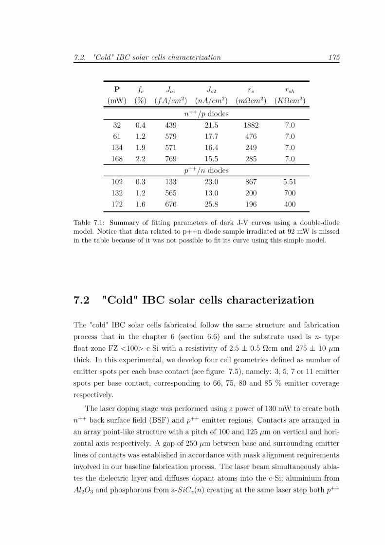
7.2. "Cold" IBC solar cells characterization 175
P fc Jo1 Jo2 rs rsh
(mW) (%) (fA/cm2) (nA/cm2) (mΩcm2) (KΩcm2)
n++/p diodes
32 0.4 439 21.5 1882 7.0
61 1.2 579 17.7 476 7.0
134 1.9 571 16.4 249 7.0
168 2.2 769 15.5 285 7.0
p++/n diodes
102 0.3 133 23.0 867 5.51
132 1.2 565 13.0 200 700
172 1.6 676 25.8 196 400
Table 7.1: Summary of fitting parameters of dark J-V curves using a double-diodemodel. Notice that data related to p++n diode sample irradiated at 92 mW is missedin the table because of it was not possible to fit its curve using this simple model.
7.2 "Cold" IBC solar cells characterization
The "cold" IBC solar cells fabricated follow the same structure and fabrication
process that in the chapter 6 (section 6.6) and the substrate used is n- type
float zone FZ <100> c-Si with a resistivity of 2.5 ± 0.5 Ωcm and 275 ± 10 µm
thick. In this experimental, we develop four cell geometries defined as number of
emitter spots per each base contact (see figure 7.5), namely: 3, 5, 7 or 11 emitter
spots per base contact, corresponding to 66, 75, 80 and 85 % emitter coverage
respectively.
The laser doping stage was performed using a power of 130 mW to create both
n++ back surface field (BSF) and p++ emitter regions. Contacts are arranged in
an array point-like structure with a pitch of 100 and 125 µm on vertical and hori-
zontal axis respectively. A gap of 250 µm between base and surrounding emitter
lines of contacts was established in accordance with mask alignment requirements
involved in our baseline fabrication process. The laser beam simultaneously abla-
tes the dielectric layer and diffuses dopant atoms into the c-Si; aluminium from
Al2O3 and phosphorous from a-SiCx(n) creating at the same laser step both p++
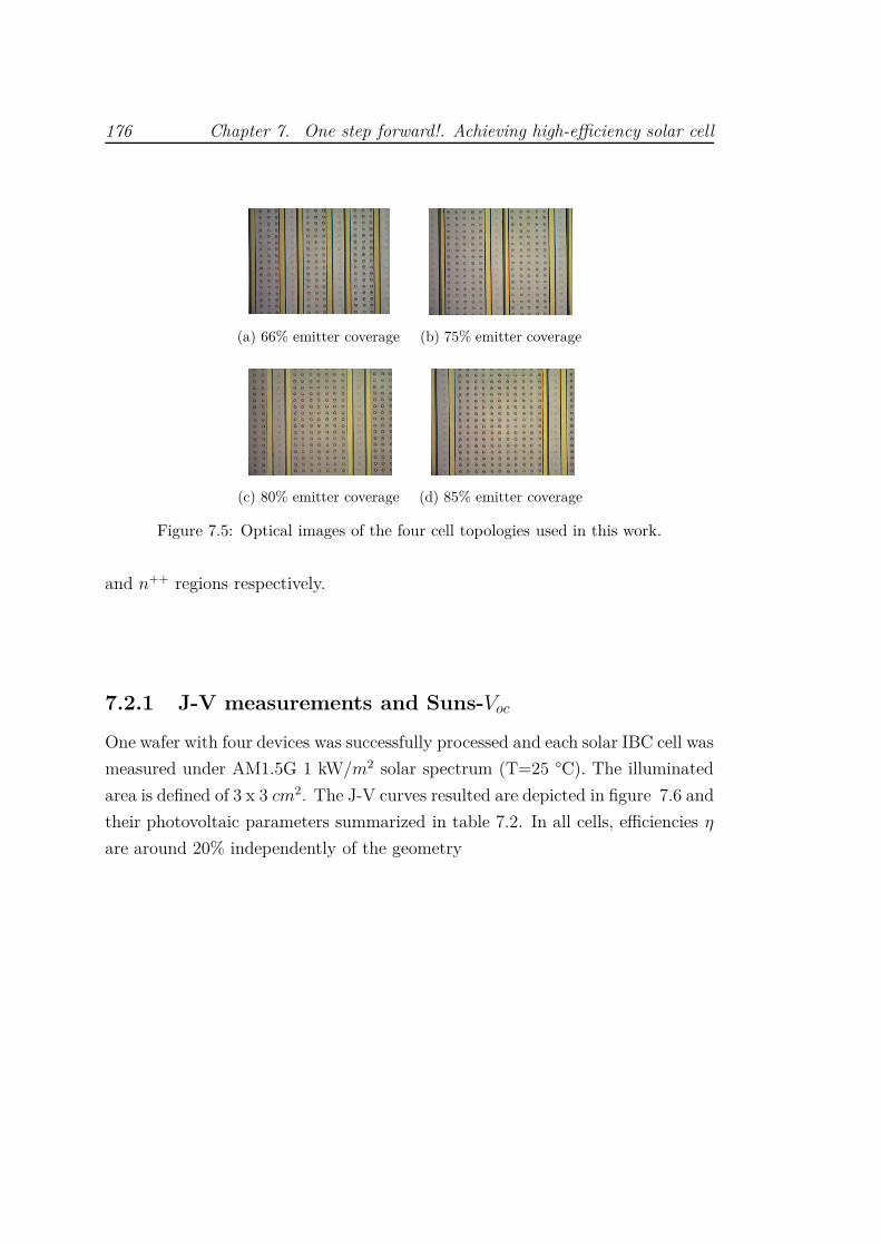
176 Chapter 7. One step forward!. Achieving high-efficiency solar cell
(a) 66% emitter coverage (b) 75% emitter coverage
(c) 80% emitter coverage (d) 85% emitter coverage
Figure 7.5: Optical images of the four cell topologies used in this work.
and n++ regions respectively.
7.2.1 J-V measurements and Suns-Voc
One wafer with four devices was successfully processed and each solar IBC cell was
measured under AM1.5G 1 kW/m2 solar spectrum (T=25 °C). The illuminated
area is defined of 3 x 3 cm2. The J-V curves resulted are depicted in figure 7.6 and
their photovoltaic parameters summarized in table 7.2. In all cells, efficiencies η
are around 20% independently of the geometry

7.2. "Cold" IBC solar cells characterization 177
0
5
10
15
20
25
30
35
40
45
0 0.2 0.4 0.6
Cu
rren
t den
sity
(m
A/c
m2)
Voltage (V)
1E-07
1E-06
1E-05
1E-04
1E-03
1E-02
1E-01
1E+00
-0.7 -0.5 -0.3 -0.1 0.1 0.3 0.5 0.7
Dark J-V
(a) 66% emitter coverage
0
5
10
15
20
25
30
35
40
45
0 0.2 0.4 0.6
Cu
rren
t den
sity
(m
A/c
m2)
Voltage (V)
1E-07
1E-06
1E-05
1E-04
1E-03
1E-02
1E-01
1E+00
-0.7 -0.5 -0.3 -0.1 0.1 0.3 0.5 0.7
Dark J-V
(b) 75% emitter coverage
0
5
10
15
20
25
30
35
40
45
0 0.2 0.4 0.6
Cu
rren
t den
sity
(m
A/c
m2)
Voltage (V)
1E-07
1E-06
1E-05
1E-04
1E-03
1E-02
1E-01
1E+00
-0.7 -0.5 -0.3 -0.1 0.1 0.3 0.5 0.7
Dark J-V
(c) 80% emitter coverage
0
5
10
15
20
25
30
35
40
45
0 0.2 0.4 0.6
Cu
rren
t den
sity
(m
A/c
m2)
Voltage (V)
1E-07
1E-06
1E-05
1E-04
1E-03
1E-02
1E-01
1E+00
-0.7 -0.5 -0.3 -0.1 0.1 0.3 0.5 0.7
Dark J-V
(d) 85% emitter coverage
Figure 7.6: J-V measurements of the four "cold" IBC fabricated as a function of theemitter coverage. Dark J-V characteristics are also included in the inset
The high Jsc values achieved suggest that front surface passivation is preserved
after the CF4 etching, the laser-stage and rear e-beam metallization as it is also
confirmed by observing the external quantum efficiency EQE curves in figure
7.7a. In figure 7.7b the EQE, reflectance and calculated IQE of the best cell
(75% emitter coverage) are shown.
EQE values up to 98% in the visible wavelength range not only require an
excellent front surface passivation, but also a negligible electrical shadowing due
to a poor passivation at the rear side including the base n++ contacts. Excellent
rear passivation explains the scarcely influence of emitter coverage in the Jsc
parameter. The relevant decay in the UV-VIS (300-600 nm) and the near IR (>
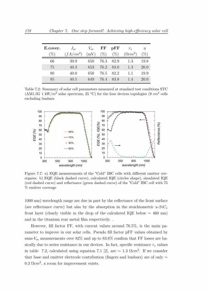
178 Chapter 7. One step forward!. Achieving high-efficiency solar cell
E.cover. Jsc Voc FF pFF rs η
(%) (fA/cm2) (mV) (%) (%) (Ωcm2) (%)
66 39.9 650 76.3 82.9 1.3 19.8
75 40.3 653 76.2 83.0 1.3 20.0
80 40.0 650 76.5 82.2 1.1 19.9
85 40.5 649 76.4 83.8 1.4 20.0
Table 7.2: Summary of solar cell parameters measured at standard test conditions STC(AM1.5G 1 kW/m2 solar spectrum, 25 °C) for the four devices topologies (9 cm2 cellsexcluding busbars
0
10
20
30
40
50
60
70
80
90
100
300 550 800 1050
EQ
E (%
)
wavelength (nm)
66%
75%
80%
85%
0
10
20
30
40
50
60
70
80
90
100
300 550 800 1050R
eflecta
nce (%
)
EQ
E (%
), IQ
E(%
)
wavelength (nm)
Figure 7.7: a) EQE measurements of the "Cold" IBC cells with different emitter cov-ergares. b) EQE (black dashed curve), calculated IQE (circles shape), simulated IQE(red dashed curve) and reflectance (green dashed curve) of the "Cold" IBC cell with 75% emitter coverage
1000 nm) wavelength range are due in part by the reflectance of the front surface
(see reflectance curve) but also by the absorption in the stoichiometric a-SiCx
front layer (clearly visible in the drop of the calculated IQE below ∼ 460 nm)
and in the titanium rear metal film respectively. .
However, fill factor FF, with current values around 76.5%, is the main pa-
rameter to improve in our solar cells. Pseudo fill factor pFF values obtained by
suns-Voc measurements over 82% and up to 83.8% confirm that FF losses are ba-
sically due to series resistance in our devices. In fact, specific resistance rs values
in table 7.2, calculated using equation 7.1 [2], are ∼ 1.3 Ωcm2. If we consider
that base and emitter electrode contribution (fingers and busbars) are of only ∼
0.3 Ωcm2, a room for improvement exists.

7.2. "Cold" IBC solar cells characterization 179
rs ≃ (1 −FF
pFF) ×
Voc
Jsc
(7.1)
In order to find the origin of the high ohmic losses, we compare J-V curves
under illumination and normalized by Jsc, with a counterpart device where the
only difference is the horizontal pitch between emitter contacts of 250 µm (double
pitch) (see figure 7.8). It is clear that reducing the pitch by a factor of two
improves noticeable the J-V curve and the FF. Note that the current drop for low
voltages in the 250 µm pitch curve compared with the 125 µm pitch counterpart
is not caused by a hypothetical shunt in that device, as it can be seen in the dark
J-V characteristics shown in the inset of 7.8. This fact suggest that the main
contribution on series resistance might be due to a very resistive p- channel around
emitter p++ contacts induced by the negative charge in the Si/Al2O3 interface.
This induced pn junction around emitter contacts improve photocarrier collection
in the cell, but has a negative effect in rs.
0.0 0.1 0.2 0.3 0.4 0.5 0.6 0.70.0
0.2
0.4
0.6
0.8
1.0
Voltage V (V)
125 µm 250 µm
Norm
aliz
ed c
urr
ent densi
ty J
/J sc
( )
-0.4 0.0 0.4 0.810
-6
10-5
10-4
10-3
10-2
10-1
Curr
ent densi
ty J
(A
/cm
2)
Voltage V (V)
Figure 7.8: Normalized J/Jsc − V characteristics of the best IBC cell (75% emittercoverage) compared with a counterpart device with a higher horizontal pitch in emitterregions (250 µm). Dark J-V characteristics for both cells are also included in the inset.

180 Chapter 7. One step forward!. Achieving high-efficiency solar cell
This pernicious impact on rs might be reduced by bringing closer even more
emitter contacts (decrease pitch in emitter regions) without jeopardizing recombi-
nation current density Jo, i.e. Voc, of the solar cell using for instance even smaller
point contacts (reducing Din and/or Dout). This aspect is another important
point to be study in future works, where the election of the laser system will play
a crucial role in the optimization of this type of solar cell structures.
7.3 Conclusions
A novel interdigitated back contacted (IBC) solar cell structure on c-Si(n) subs-
trates has been proposed using a fully low-temperature fabrication process based
on laser-doped point-like contacts. Emitter and base contacts are created in a sin-
gle UV laser processing stage. Low-temperature deposited Al2O3 and a-SiCx(n)
stacks provide both the aluminum and phosphorous doping atoms respectively,
and excellent front and rear passivation. The fabrication process sequence in-
volved in our lab cells is very simple with only two photolithography patterning
stages which might be replaced in an industrial feasible process using standard
serigraphy, laser ablation or selective deposition by means of metal masks. The
final devices reach to a promising efficiencies up to 20% with short-circuit current
densities and open circuit voltages of around 40 mA/cm2 and 650 mV respec-
tively. Efficiency is mainly limited by series resistance with fill factor FF values
around 76.5% and relatively high pseudo-FF (pFF) values over 82% and up to
83.8%. Main ohmic losses are probably due to an induced p-type floating channel
surrounding p++ emitter contacts provided by the negative charge inherent on
Al2O3/Si interfaces. Additional efficiency losses are due to reflectance and para-
sitic absorption of the SiCx and Ti layers present on front antireflection coating
and back reflector stacks respectively.
Bibliography 181
Bibliography
[1] A. Roigé, J.O. Ossó, I. Martín, C. Voz, P. Ortega, J.M. López-González, and
L.F. Alcubilla, R. Vega. Microscale characterization of surface recombination
at the vicinity of laser-processed regions in c-Si solar cells. IEEE Journal of
Photovoltaics, 6(2):426–431, 2016.
[2] Martin Green. Solar cells: Operating Principles, Technology and System Ap-
plications. UNSW, pp.96, 1998.


Chapter 8
Summary and Future Work
8.1 Summary
In this thesis a new concept of high-efficiency interdigitated back-contact (IBC)
solar cells for one-sun applications have been developed. Laser doping technique
through dielectric layers has been employed to create highly doped regions (n++
and p++) in a point-like structure on c-Si wafers and following four different
emitter coverage. A innovative stack of dielectric layers has allowed to simplify
the multiple and complex structuring steps traditionally used to form the n- and
p-doped regions and the grid metal contacts. The two different dielectric stacks
used in this work consisted of:
• Al2O3+ stoichiomentric carbon rich a-SiCx
• intrinsic a-SiCx+ a-Si phosphorous doped+ stoichiometric carbon rich a-
SiCx
Both layers have been studied and optimized to act simultaneously as passi-
vatting layer and dopant source of aluminum and phosphorous respectively and
to form the p++ and the n++ regions.
Additionally, the total elimination of the conventional high-temperature diffu-
sion combined with the reduction of the complex and costly photolithographic
masking steps have allowed to reduce the time-consuming fabrication process and
the high cost associated to high temperature.
Special attention has been paid to the surface passivation (polished and tex-
tured c-silicon) achievable with Al2O3 deposited by thermal ALD. A detailed
183

184 Chapter 8. Summary and Future Work
studied was carried out in order to know the influence of thickness film, deposition
temperature and time/temperature of annealing on the surface recombination ve-
locity. The surface passivation study was also extended to Al2O3/stoichiometric
carbon rich a-SiCx stack (the last layer deposited by PECVD) due to its final
implementation on the final device. The study has demonstrated an outstanding
Seff,max below 15 cm/s independently of the surface morphology and doping type.
Additionally, optical properties measurements have revealed that 90 nm of Al2O3
deposited on textured c-Si surface are optimal for antireflection purposes while
the combination of Al2O3+ stoichiometric a−SiCx with different thickness com-
bination shows some absorption by the capping layer below 460 nm. Although
this absorption, all the stack configuration show a low Jsc loss lower than 2%
between 460 to 1025 nm.
Concerning the electrical quality of the p+/n and n+/p junctions, we have
fabricated diodes applying different laser conditions to the two dielectric stacks.
We have varied the number of pulses and laser power while the pulse duration
and frequency were fixed to 100 ns and 4Khz respectively. Systematical dark J-V
measurements were done to electrically characterize the diodes concluding that
the best diodes were obtained with 0.9 W and 1 W (6/9 pulses) for p+/n junction
and 0.9 W (3/6 pulses) and 0.8 W/9 pulses for n+/p junction.
As a first approximation, the first p-type IBC solar cells were fabricated using
one phosphorous diffusion step and the laser processing was applied through the
dielectric layer studied. Accordingly, new precursors diodes were fabricated and
analyzed. Efficiencies up to 18.7% and Jsc of 39.2 mA/cm2 were obtained. How-
ever, low surface passivation quality and the damage induced by the laser stage
onto the silicon lattice limited the final efficiency by reducing the FF and Voc. A
calculated ideality factor of ∼1.5 agrees with carrier recombination in the space
charge region by the laser damage or the influence of parasitic shunting. Addi-
tionally, optical simulation demonstrates extra Jph losses as a consequence of the
back reflector scheme and rear films absorption.
In a second approach we eliminated the phosphorous diffusion step and we
developed the first n-type "Cold" IBC solar cells in which all the highly-doped
regions were entirely fabricated by infrared laser processing through the dielectric

8.1. Summary 185
layers. Additionally, the dielectric stacks were strategically modified in order to
reduce the number of patterning steps to only two. The dielectric layers em-
ployed as dopant sources were the same than those used in the "Hybrid" IBC, i.e.
Al2O3 to dope p++ regions and a-SiCx(n) the n++. "Cold" IBCs were fabricated
in two different batches following the same fabrication process. In the first one,
the punctual contacts were done in two laser steps. The emitter contacts (p++)
were done with 6 pulses and a laser pulse duration of 100 ns. The power applied
was 1100 mW. The base contacts were done at 1070 mW with a pulse duration of
400 ns. Efficiencies from 12% to 15.5% depending of the emitter coverage were
obtained. However, the low FF, Voc and Jsc point to a poor surface passivation
and damage-induced laser. The second batch was focused on a better passiva-
tion quality control after CF4 etching and laser stage improvement. The surface
passivation quality was maintained along the whole fabrication process and the
laser stage was modified applying a pulse duration of 400 ns at 1020 mW in one
single step to form both emitter and base contacts. General improvement was
achieved in the final devices. Efficiencies from 17.3 to 18.0% and Jsc up to 39.2
mA/cm2 were obtained. Unfortunately, the low FF and Voc still limited the final
η mainly due to the laser processing step and the instability of the power laser.
Consequently, the used laser power was above the optimum power in order to
form all the doped contacts.
Finally, we developed the last "Cold" IBC solar cells changing the laser pro-
cessing type. We applied UV laser (355 nm), with a pulse duration and frequency
of 12 ns and 20kHz respectively in one single laser step to form BSF and emitter
regions simultaneously. Due to the smaller spots, the pitch could be decreased to
125 µm. The power laser was controlled by means of an external attenuator and
the optimum value was found 130 mW. As a result, the photovoltaic parameters
were improved. Efficiencies up to 20% using this simplified baseline process ex-
hibited short-circuit densities and open-circuit voltages about 40 mA/cm2 and
650 mV respectively. However, efficiencies are mainly limited by series resistance
limiting fill factor FF values around 76.5% with relatively high pseudo-FF (pFF)
values over 82% and up to 83.8%. Main ohmic losses are probably due to an
induced p-type floating channel surrounding p++ emitter contacts provided by
the negative charge inherent on Al2O3/Si interfaces.

186 Chapter 8. Summary and Future Work
8.2 Future works
Efficiencies beyond 22% are feasible by future improvements in the fabrication
process addressed to overcome some optical and series resistance losses in our
current devices. In particular:
• Overcome optical losses by replacing the front absorbent layer (stoichiome-
tric a-SiCx) by non-absorbent a-SiNx and/or introducing new single-side
texturing technique based for instance on black silicon which can boost
efficiency about 1% absolute in the future.
• Selecting a laser system which allow small contacts and reduce pitches might
reduce p-channel effect decreasing series resistance and improving FF accor-
dingly without jeopardizing Jsc and Voc.
• Simplify even more the fabrication process avoiding the thermal oxidation
texturing simultaneously both surfaces.
• Substitute the rear metal contacts of Ti/Al stack by another metal confi-
guration to avoid the rear film absorption.
• To eliminate the photolithographic step to form the metal pattern and to
substitute it by laser ablation.

8.3. List of publications 187
8.3 List of publications
8.3.1 Refereed journal paper
• G. López, P. Ortega, I. Martín, C. Voz, A. Orpella, R. Alcubilla, "Cold
process for IBC c-Si solar cells fabrication" Energy Procedia,
92:652-660, 2016.
• G. López, P. Ortega, I. Martín, C. Voz, A. Morales-Vilches, A. Orpella, R.
Alcubilla, "Base contacts and selective emitters processed by laser doping
technique for p-type IBC c-Si solar cells" Energy Procedia, 77:752-758, 2015
• G. López, P. Ortega, C. Voz, I. Martín, A. Morales-Vilches, A. Orpella,
R. Alcubilla, " Emitter formation using laser doping technique on n- and
p-type c-Si substrates" Applied Surface Science, 336:182-187, 2015
• G. López, P. Ortega, C. Voz, I. Martín, M. Colina, A. Morales-Vilches,
A. Orpella, and R. Alcubilla "Surface passivation and optical characteri-
zation of Al2O3/a − SiCx stacks on c-Si substrates. Beilstein journal of
nanotechnology, 4:726-31, 2013
8.3.2 Other related publications
Falta publicacion de Isi y Gerard
• G. Masmitja, P. Ortega, I. Martín, G. López, C. Voz, R. Alcubilla, "IBC
c-Si(n) solar cells based on laser doping processing for selective emitter and
base contact formation", Energy Procedia, 92C:956-961, 2016
• A. Morales-Vilches, C. Voz, M. Colina, D. Munoz-Martin, I. Martin, P.
Ortega, G. Lopez, C. Molpeceres, and R. Alcubilla. "Study of the surface
recombination velocity for ultraviolet and visible laser-fired contacts applied
to silicon heterojunction solar cells". IEEE Journal of Photovoltaics, 5:1006-
1013, 2015
• M. Colina, A. Morales-Vilches, C. Voz, I. Martín, P. Ortega, A. Orpella,
G. López, R. Alcubilla. "Laser Induced Forward Transfer for front contact
improvement in silicon heterojunction solar cells". Energy Procedia, 336:89-
95, 2015

188 Chapter 8. Summary and Future Work
• I. Martín, A. Coll, G. López, P. Ortega, T. Desrues, A. Orpella, R. Alcubilla.
"TCO-free Low-temperature p+ Emitters for Back-junction c-Si Solar Cells".
Energy Procedia, 77:296-303, 2015
• I. Martín, M. Colina, A. Coll, G. López, P. Ortega, A. Orpella, R. Alcubilla.
"c-Si solar cells based on laser-processed dielectric films". Energy Procedia,
55:255-264, 2014
• M. Colina, I. Martín, C. Voz , A. Morales-Vilches , P. Ortega, G. López, A.
Orpella, M. García-Molina, D. MuÃśoz-Martín, M.I. Sánchez-Aniorte, C.
Molpeceres, R. Alcubilla. " Optimization of Laser Processes for Local Rear
Contacting of Passivated Silicon Solar Cells". Energy Procedia, 44:234-243,
2014
• D. Carrió, P. Ortega, I. Martín, G. López, J. M. López-González, A. Orpella,
C. Voz, R. Alcubilla. "Rear contact pattern optimization based on 3D
simulations for IBC solar cells with point-like doped contacts". Energy
Procedia, 55:47-52, 2014
• A. Morales-Vilches, C. Voz, M. Colina, G. López, I. Martín, P. Ortega, A.
Orpella, R. Alcubilla. "Recovery of Indium-tin-oxide/silicon Heterojunction
Solar Cells by Thermal Annealing". Energy Procedia, 44:3-9, 2014
• P. Ortega, I. Martin, G. Lopez, M. Colina, A. Orpella, C. Voz, R. Alcubilla.
"p-type c-Si solar cells based on rear side laser processing of Al2O3/SiCx
stacks". Solar energy materials and solar cells, 106:80-83, 2012
• I. Martín, P. Ortega, M. Colina, A. Orpella, G. López, R. Alcubilla."Laser
processing of Al2O3/a − SiCx : H stacks: a feasible solution for the rear
surface of high-efficiency p-type c-Si solar cells".
Progress in Photovoltaics:Research and Applications, 21:1171-1175, 2012
• P. Ortega, A. Orpella, I. Martin, M. Colina, G. Lopez, C. Voz, I. Sánchez,
C. Molpeceres, R. Alcubilla. "Laser-fired contact optimization in c-Si solar
cells". Progress in photovoltaics, 20(2):173-180, 2012
8.3.3 National and International conferences
• G. López, P. Ortega, I. Martín, C. Voz, A. Orpella, R. Alcubilla, "Cold
process for IBC c-Si solar cells fabrication", SiliconPV 2016, the 6th Inter-
8.3. List of publications 189
national Conference on Silicon Photovoltaics, 7-9 March 2016, Chambéry
(France)
• G. Masmitja, P. Ortega, I. Martín, G. López, C. Voz, R. Alcubilla, "IBC
c-Si(n) solar cells based on laser doping processing for selective emitter and
base contact formation", SiliconPV 2016, the 6th International Conference
on Silicon Photovoltaics, 7-9 March 2016, Chambéry (France)
• E. Calle, P. Ortega, G. Lopez, I. Martin, D. Carrió, C. Voz, A. Orpella, J.
Puigdollers, R. Alcubilla. "High efficiency interdigitated back-contact c-Si
solar cells". 10th Spanish Conference on Electron Devices, CDE 2015, 11-13
February 2015, Aranjuez-Madrid (Spain)
• G. López, P. Ortega, I. Martín, C. Voz, A. Morales-Vilches, A. Orpella, R.
Alcubilla, "Base contacts and selective emitters processed by laser doping
technique for p-type IBC c-Si solar cells", SiliconPV 2015, 5th Interna-
tional Conference on Silicon Photovoltaics, 23-25 March 2015, Konstanz
(Germany)
• I. Martín, A. Coll, G. López, P. Ortega, T. Desrues, A. Orpella, R. Alcubilla.
"TCO-free Low-temperature p+ Emitters for Back-junction c-Si Solar Cells",
SiliconPV 2015, 5th International Conference on Silicon Photovoltaics, 23-
25 March 2015, Konstanz (Germany)
• I. Martín, M. Colina, A. Coll, G. López, P. Ortega, A. Orpella, R. Alcubilla.
"c-Si solar cells based on laser-processed dielectric films", SiliconPV 2014,
4th International Conference on Silicon Photovoltaics, 25-27 March 2014,
s-Hertogenbosch (Netherlands)
• G. López, P. Ortega, C. Voz, I. Martín, A. Morales-Vilches, A. Orpella,
R. Alcubilla, " Emitter formation using laser doping technique on n- and
p-type c-Si substrates" E-MRS Spring Meeting 2014, 26-30 May 2014, Lille
(France)
• M. Colina, I. Martín, C. Voz , A. Morales-Vilches , P. Ortega, G. López,
A. Orpella, M. García-Molina, D. Muñoz-Martín, M.I. Sánchez-Aniorte, C.
Molpeceres, R. Alcubilla. " Optimization of Laser Processes for Local Rear
Contacting of Passivated Silicon Solar Cells", E-MRS Spring Meeting 2013,
27-31 May 2013, Strasbourg (France)
190 Chapter 8. Summary and Future Work
• A. Morales-Vilches, C. Voz, M. Colina, G. López, I. Martín, P. Ortega, A.
Orpella, R. Alcubilla. "Recovery of Indium-tin-oxide/silicon Heterojunction
Solar Cells by Thermal Annealing", E-MRS Spring Meeting 2013, 27-31 May
2013, Strasbourg (France)
• G. López, P. Ortega, C. Voz, I. Martín, M. Colina, A. Morales-Vilches, A.
Orpella, and R. Alcubilla. "Surface passivation and optical characterization
of Al2O3/a − SiCx stacks on c-Si substrates", E-MRS Spring Meeting 2013,
27-31 May 2013, Strasbourg (France)
• D. Carrió, P. Ortega, G. López, J. Lopez-Gonzalez, I. Martin, C. Voz, R.
Alcubilla. "3D simulations of back-contact back-junction c-Si(P) solar cells
with doped point contacts". European Photovoltaic Solar Energy Confer-
ence and Exhibition, 28th PVSEC, 30 September 2013, Paris (France)
• G. Masmitja, P. Ortega, G. López, E. Calle, M. García, I. Martín, A. Or-
pella, C. Voz, R. Alcubilla. "Boron diffused emitters passivated with Al2O3
films, 9th Spanish Conference on Electron Devices, CDE 2013, 12-14 Febru-
ary, Valladolid (Spain)
• P. Ortega, R. Jové, A. Pedret, G. Gonzalvez, G. López, I. Martín, M.
Domínguez, R. Alcubilla, A. Camps." An IBC solar cell for the UPC
CubeSat-1 mission". 9th Spanish Conference on Electron Devices, CDE
2013, 12-14 February, Valladolid (Spain)
• A. Morales-Vilches, C. Voz, M. Colina, G. Lopez, I. Martin, A. Orpella, J.
Puigdollers, M. Garcia, and R. Alcubilla. "Progress in silicon heterojunction
solar cell fabrication with rear laser-fired contacts". 9th Spanish Conference
on Electron Devices, CDE 2013, 12-14 February, Valladolid (Spain)
• C. Molpeceres, M. Colina, D. Muñoz-Martin, I. Martín, P. Ortega, I. Sánchez,
M. Morales, S. Lauzurica, J. García-Ballesteros, C. Voz, G. López, A.
Morales, R. Alcubilla. " New laser-based approaches to improve the pa-
ssivation and rear contact quality in high efficiency crystalline silicon solar
cells", SPIE Optics+Photonics. Proceedings SPIE Vol. 8826". San Diego:
2013, p. 882603-1-882603-11
• M. Colina, I. Martín, C. Voz, A. Morales-Vilches, P. Ortega, G. López,
A. Orpella, R. Alcubilla, I. Sánchez-Aniorte, C. Molpeceres. "Optimiza-

8.3. List of publications 191
tion of laser doping processes for the creation of p+ regions from solid
dopant sources", European Photovoltaic Solar Energy Conference and Ex-
hibition,27th PVSEC, 24-28 September 2012, Frankfurt (Germany)
• G.Lopez, P. Ortega, I. Martin, M. Colina, A. Orpella, R. Alcubilla. "Op-
timization of Al2O3 films obtained by ALD to passivate p-type c-silicon
wafers", European Photovoltaic Solar Energy Conference and Exhibition,
27th PVSEC, 24-28 September 2012, Frankfurt (Germany)
Recommended


